WO2023218548A1 - 放電電極、アノードの製造方法、及び電子デバイスの製造方法 - Google Patents
放電電極、アノードの製造方法、及び電子デバイスの製造方法 Download PDFInfo
- Publication number
- WO2023218548A1 WO2023218548A1 PCT/JP2022/019914 JP2022019914W WO2023218548A1 WO 2023218548 A1 WO2023218548 A1 WO 2023218548A1 JP 2022019914 W JP2022019914 W JP 2022019914W WO 2023218548 A1 WO2023218548 A1 WO 2023218548A1
- Authority
- WO
- WIPO (PCT)
- Prior art keywords
- width
- region
- discharge
- discharge electrode
- anode
- Prior art date
- Legal status (The legal status is an assumption and is not a legal conclusion. Google has not performed a legal analysis and makes no representation as to the accuracy of the status listed.)
- Ceased
Links
Images





Classifications
-
- H—ELECTRICITY
- H01—ELECTRIC ELEMENTS
- H01S—DEVICES USING THE PROCESS OF LIGHT AMPLIFICATION BY STIMULATED EMISSION OF RADIATION [LASER] TO AMPLIFY OR GENERATE LIGHT; DEVICES USING STIMULATED EMISSION OF ELECTROMAGNETIC RADIATION IN WAVE RANGES OTHER THAN OPTICAL
- H01S3/00—Lasers, i.e. devices using stimulated emission of electromagnetic radiation in the infrared, visible or ultraviolet wave range
- H01S3/02—Constructional details
- H01S3/03—Constructional details of gas laser discharge tubes
- H01S3/0305—Selection of materials for the tube or the coatings thereon
-
- H—ELECTRICITY
- H01—ELECTRIC ELEMENTS
- H01S—DEVICES USING THE PROCESS OF LIGHT AMPLIFICATION BY STIMULATED EMISSION OF RADIATION [LASER] TO AMPLIFY OR GENERATE LIGHT; DEVICES USING STIMULATED EMISSION OF ELECTROMAGNETIC RADIATION IN WAVE RANGES OTHER THAN OPTICAL
- H01S3/00—Lasers, i.e. devices using stimulated emission of electromagnetic radiation in the infrared, visible or ultraviolet wave range
- H01S3/02—Constructional details
- H01S3/03—Constructional details of gas laser discharge tubes
- H01S3/036—Means for obtaining or maintaining the desired gas pressure within the tube, e.g. by gettering, replenishing; Means for circulating the gas, e.g. for equalising the pressure within the tube
-
- H—ELECTRICITY
- H01—ELECTRIC ELEMENTS
- H01S—DEVICES USING THE PROCESS OF LIGHT AMPLIFICATION BY STIMULATED EMISSION OF RADIATION [LASER] TO AMPLIFY OR GENERATE LIGHT; DEVICES USING STIMULATED EMISSION OF ELECTROMAGNETIC RADIATION IN WAVE RANGES OTHER THAN OPTICAL
- H01S3/00—Lasers, i.e. devices using stimulated emission of electromagnetic radiation in the infrared, visible or ultraviolet wave range
- H01S3/02—Constructional details
- H01S3/03—Constructional details of gas laser discharge tubes
- H01S3/038—Electrodes, e.g. special shape, configuration or composition
-
- H—ELECTRICITY
- H01—ELECTRIC ELEMENTS
- H01S—DEVICES USING THE PROCESS OF LIGHT AMPLIFICATION BY STIMULATED EMISSION OF RADIATION [LASER] TO AMPLIFY OR GENERATE LIGHT; DEVICES USING STIMULATED EMISSION OF ELECTROMAGNETIC RADIATION IN WAVE RANGES OTHER THAN OPTICAL
- H01S3/00—Lasers, i.e. devices using stimulated emission of electromagnetic radiation in the infrared, visible or ultraviolet wave range
- H01S3/02—Constructional details
- H01S3/03—Constructional details of gas laser discharge tubes
- H01S3/038—Electrodes, e.g. special shape, configuration or composition
- H01S3/0381—Anodes or particular adaptations thereof
-
- H—ELECTRICITY
- H01—ELECTRIC ELEMENTS
- H01S—DEVICES USING THE PROCESS OF LIGHT AMPLIFICATION BY STIMULATED EMISSION OF RADIATION [LASER] TO AMPLIFY OR GENERATE LIGHT; DEVICES USING STIMULATED EMISSION OF ELECTROMAGNETIC RADIATION IN WAVE RANGES OTHER THAN OPTICAL
- H01S3/00—Lasers, i.e. devices using stimulated emission of electromagnetic radiation in the infrared, visible or ultraviolet wave range
- H01S3/02—Constructional details
- H01S3/03—Constructional details of gas laser discharge tubes
- H01S3/038—Electrodes, e.g. special shape, configuration or composition
- H01S3/0382—Cathodes or particular adaptations thereof
-
- H—ELECTRICITY
- H01—ELECTRIC ELEMENTS
- H01S—DEVICES USING THE PROCESS OF LIGHT AMPLIFICATION BY STIMULATED EMISSION OF RADIATION [LASER] TO AMPLIFY OR GENERATE LIGHT; DEVICES USING STIMULATED EMISSION OF ELECTROMAGNETIC RADIATION IN WAVE RANGES OTHER THAN OPTICAL
- H01S3/00—Lasers, i.e. devices using stimulated emission of electromagnetic radiation in the infrared, visible or ultraviolet wave range
- H01S3/02—Constructional details
- H01S3/03—Constructional details of gas laser discharge tubes
- H01S3/038—Electrodes, e.g. special shape, configuration or composition
- H01S3/0385—Shape
-
- H—ELECTRICITY
- H01—ELECTRIC ELEMENTS
- H01S—DEVICES USING THE PROCESS OF LIGHT AMPLIFICATION BY STIMULATED EMISSION OF RADIATION [LASER] TO AMPLIFY OR GENERATE LIGHT; DEVICES USING STIMULATED EMISSION OF ELECTROMAGNETIC RADIATION IN WAVE RANGES OTHER THAN OPTICAL
- H01S3/00—Lasers, i.e. devices using stimulated emission of electromagnetic radiation in the infrared, visible or ultraviolet wave range
- H01S3/02—Constructional details
- H01S3/03—Constructional details of gas laser discharge tubes
- H01S3/038—Electrodes, e.g. special shape, configuration or composition
- H01S3/0388—Compositions, materials or coatings
-
- H—ELECTRICITY
- H01—ELECTRIC ELEMENTS
- H01S—DEVICES USING THE PROCESS OF LIGHT AMPLIFICATION BY STIMULATED EMISSION OF RADIATION [LASER] TO AMPLIFY OR GENERATE LIGHT; DEVICES USING STIMULATED EMISSION OF ELECTROMAGNETIC RADIATION IN WAVE RANGES OTHER THAN OPTICAL
- H01S3/00—Lasers, i.e. devices using stimulated emission of electromagnetic radiation in the infrared, visible or ultraviolet wave range
- H01S3/14—Lasers, i.e. devices using stimulated emission of electromagnetic radiation in the infrared, visible or ultraviolet wave range characterised by the material used as the active medium
- H01S3/22—Gases
- H01S3/223—Gases the active gas being polyatomic, i.e. containing two or more atoms
- H01S3/225—Gases the active gas being polyatomic, i.e. containing two or more atoms comprising an excimer or exciplex
Definitions
- the present disclosure relates to a method for manufacturing a discharge electrode, an anode, and a method for manufacturing an electronic device.
- a KrF excimer laser device that outputs a laser beam with a wavelength of about 248 nm and an ArF excimer laser device that outputs a laser beam with a wavelength of about 193 nm are used.
- the spectral line width of the spontaneous oscillation light of the KrF excimer laser device and the ArF excimer laser device is as wide as 350 to 400 pm. Therefore, if the projection lens is made of a material that transmits ultraviolet light such as KrF and ArF laser light, chromatic aberration may occur. As a result, resolution may be reduced. Therefore, it is necessary to narrow the spectral linewidth of the laser beam output from the gas laser device until the chromatic aberration becomes negligible. Therefore, in order to narrow the spectral line width, a line narrowing module (LNM) including a narrowing element (etalon, grating, etc.) is installed in the laser resonator of a gas laser device. There is.
- a gas laser device whose spectral linewidth is narrowed will be referred to as a narrowband gas laser device.
- a discharge electrode is used in a gas laser device that excites a fluorine-containing laser gas by discharge, and includes a cathode and an anode.
- the anode is arranged to face the cathode, and includes an electrode base material containing metal, and a coating layer containing an insulating material and covering a part of the side surface parallel to the longitudinal direction of the electrode base material.
- the coating layer has a first portion covering a first region of the side surfaces and a second portion of the side surfaces further from the cathode in a discharge direction perpendicular to the longitudinal direction than the first region. a second portion that covers the located second region and is thicker than the first portion.
- a method for manufacturing an anode according to one aspect of the present disclosure is a method for manufacturing an anode of a discharge electrode used in a position facing a cathode in a gas laser device that excites a fluorine-containing laser gas by discharge, the anode comprising:
- the method includes a first step of forming a coating layer on the side surface parallel to the longitudinal direction of the electrode base material, and a second step of removing a portion of the coating layer so as to approximate the target shape.
- a cathode is formed in a second region of the side surface in a discharge direction perpendicular to the longitudinal direction more than the first portion covering the first region of the side surface. removing a portion of the coating layer such that a second portion covering a second region located farther from the coating layer is thicker.
- a method for manufacturing an electronic device includes generating laser light using a gas laser device including a laser chamber equipped with a discharge electrode, outputting the laser light to an exposure device, and manufacturing the electronic device.
- the method includes exposing a photosensitive substrate to laser light in an exposure apparatus.
- the discharge electrode is used in a gas laser device that excites a fluorine-containing laser gas by discharge, and includes a cathode and an anode.
- the anode is arranged to face the cathode, and includes an electrode base material containing metal, and a coating layer containing an insulating material and covering a part of the side surface parallel to the longitudinal direction of the electrode base material.
- the coating layer has a first portion covering a first region of the side surfaces and a second portion of the side surfaces further from the cathode in a discharge direction perpendicular to the longitudinal direction than the first region. a second portion that covers the located second region and is thicker than the first portion.
- FIG. 1 schematically shows the configuration of a gas laser device according to a comparative example.
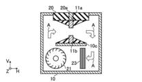
- FIG. 2 schematically shows the laser chamber shown in FIG. 1 and its internal configuration.
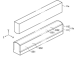
- FIG. 3 is a perspective view of the cathode and anode shown in FIGS. 1 and 2.
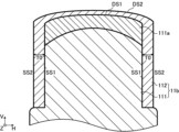
- FIG. 4 is a cross-sectional view of an anode that has been used over a long period of time.
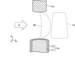
- FIG. 5 schematically shows the state of discharge between the cathode and anode in the comparative example.
- FIG. 6 schematically shows the state after the discharge between the cathode and anode shown in FIG. 5 is performed.
- FIG. 1 schematically shows the configuration of a gas laser device according to a comparative example.
- FIG. 2 schematically shows the laser chamber shown in FIG. 1 and its internal configuration.
- FIG. 3 is a perspective view of the cathode and anode shown in FIGS. 1 and 2.
- FIG. 4 is a cross-sectional view of an anode that has been
- FIG. 7 schematically shows the state of the discharge subsequent to the discharge between the cathode and the anode shown in FIG.
- FIG. 8 schematically shows the state of the discharge subsequent to the discharge between the cathode and the anode shown in FIG.
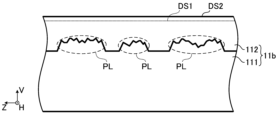
- FIG. 9 shows the side surface of the anode when the thickness of the portion of the coating layer that covers the side surface is reduced.
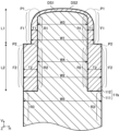
- FIG. 10 is a cross-sectional view of the anode that constitutes the discharge electrode according to the first embodiment.
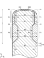
- FIG. 11 is a cross-sectional view of an anode that constitutes a discharge electrode according to the second embodiment.
- FIG. 12 is a cross-sectional view showing a manufacturing process of an anode constituting a discharge electrode according to a third embodiment.
- FIG. 13 is a cross-sectional view showing a manufacturing process of an anode constituting a discharge electrode according to a third embodiment.
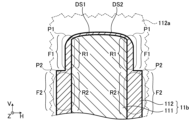
- FIG. 14 is a cross-sectional view showing a manufacturing process of an anode constituting a discharge electrode according to a fourth embodiment.
- FIG. 15 is a cross-sectional view showing a manufacturing process of an anode constituting a discharge electrode according to a fourth embodiment.
- FIG. 16 schematically shows the configuration of an exposure device connected to a gas laser device.
- FIG. 1 schematically shows the configuration of a gas laser device 1 according to a comparative example.
- the gas laser device 1 shown in FIG. 1 includes a laser chamber 10, a cathode 11a and an anode 11b constituting a pair of discharge electrodes, a charger 12, a pulsed power module (PPM) 13, a band narrowing module 14, It includes an output coupling mirror 15 and a laser controller 30.
- Band narrowing module 14 and output coupling mirror 15 constitute an optical resonator.
- the laser chamber 10 is placed in the optical path of the optical resonator.
- PPM pulsed power module
- the internal structure of the laser chamber 10 seen from a direction substantially perpendicular to the discharge direction between the cathode 11a and the anode 11b and substantially perpendicular to the traveling direction of the laser light output from the output coupling mirror 15 is shown. It is shown.
- FIG. 2 schematically shows the laser chamber 10 shown in FIG. 1 and its internal configuration.
- the internal configuration of the laser chamber 10 is shown as viewed from a direction substantially parallel to the traveling direction of the laser beam output from the output coupling mirror 15.
- the traveling direction of the laser beam output from the output coupling mirror 15 is assumed to be the +Z direction.
- the discharge direction between the cathode 11a and the anode 11b is the +V direction or the -V direction.
- the +Z direction and the +V direction are directions perpendicular to each other. A direction perpendicular to both of these is defined as a +H direction or a -H direction.
- the -V direction almost coincides with the direction of gravity.
- the laser chamber 10 accommodates a cathode 11a, an anode 11b, a crossflow fan 21, and a heat exchanger 23.
- An opening is formed in a part of the laser chamber 10, and this opening is closed by an electrically insulating part 20.
- Electrical insulation section 20 supports cathode 11a.
- a plurality of conductive parts 20a are embedded in the electrically insulating part 20. Each of the conductive parts 20a is electrically connected to the cathode 11a.
- a return plate 10c is arranged inside the laser chamber 10.
- Anode 11b is supported by return plate 10c.
- the anode 11b is electrically connected to ground potential via the return plate 10c and the conductive member of the laser chamber 10.
- the return plate 10c has gaps for the laser gas to pass through on the depth side and the front side of the page of FIG.
- the rotation shaft of the crossflow fan 21 is connected to a motor 22 placed outside the laser chamber 10.
- the motor 22 rotates the cross flow fan 21.
- the laser gas circulates inside the laser chamber 10 as shown by arrow A in FIG.
- the heat exchanger 23 discharges the thermal energy of the laser gas, which has become high in temperature due to the discharge, to the outside of the laser chamber 10 .
- the laser chamber 10 is filled with a laser gas containing, for example, argon gas or krypton gas as a rare gas, fluorine gas as a halogen gas, and neon gas as a buffer gas.
- a laser gas containing fluorine gas and buffer gas may be sealed. Windows 10a and 10b are provided at both ends of the laser chamber 10.
- the charger 12 holds electrical energy to be supplied to the pulse power module 13.
- the pulse power module 13 includes a charging capacitor (not shown) and a switch 13a.
- a charging capacitor of a pulse power module 13 is connected to the charger 12 .
- a cathode 11a is connected to a charging capacitor of the pulse power module 13 via a conductive portion 20a.
- FIG. 3 is a perspective view of the cathode 11a and anode 11b shown in FIGS. 1 and 2.
- the longitudinal direction of each of the cathode 11a and the anode 11b is approximately parallel to the Z axis.
- the anode 11b is disposed facing the cathode 11a at a position in the ⁇ V direction when viewed from the cathode 11a.
- FIG. 3 the vicinity of both longitudinal ends of each of the cathode 11a and the anode 11b is shown, and a part of the center is omitted.
- the anode 11b includes an electrode base material 111 containing metal, and a coating layer 112 that covers a part of the surface of the electrode base material 111 and contains an insulating material.
- the coating layer 112 is, for example, a thermally sprayed film of copper and alumina.
- Side surface SS1 of electrode base material 111 and side surface SS2 of coating layer 112 are parallel to both the longitudinal direction of electrode base material 111 and the discharge direction.
- the discharge surface of the electrode base material 111 facing the cathode 11a is referred to as a first discharge surface DS1.
- the discharge surface of the coating layer 112 facing the cathode 11a is referred to as a second discharge surface DS2.
- the discharge surface refers to a surface that faces another electrode that forms a pair as a discharge electrode.
- the first discharge surface DS1 is covered with the coating layer 112, discharge does not necessarily occur on the first discharge surface DS1.
- the band narrowing module 14 includes a prism 14a and a grating 14b.
- a high reflection mirror may be used instead of the band narrowing module 14.
- the output coupling mirror 15 is made of a material that transmits light of the wavelength selected by the band narrowing module 14, and one surface thereof is coated with a partially reflective film.
- the laser controller 30 receives target pulse energy setting data and a light emission trigger signal from the exposure apparatus 100 (see FIG. 16). The laser controller 30 transmits charging voltage setting data to the charger 12 based on the target pulse energy setting data. Further, the laser controller 30 transmits a trigger signal to the pulse power module 13 based on the light emission trigger signal.
- the pulse power module 13 When the pulse power module 13 receives a trigger signal from the laser controller 30, it generates a pulsed high voltage from the electrical energy charged in the charger 12, and applies this high voltage between the cathode 11a and the anode 11b.
- Light generated within the laser chamber 10 is emitted to the outside of the laser chamber 10 via windows 10a and 10b.
- the light emitted from the window 10a of the laser chamber 10 has its beam width in the H-axis direction expanded by the prism 14a, and then enters the grating 14b.
- Light that enters the grating 14b from the prism 14a is reflected by the plurality of grooves in the grating 14b and is diffracted in a direction according to the wavelength of the light.
- the prism 14a reduces the beam width of the diffracted light from the grating 14b in the H-axis direction, and returns the light to the laser chamber 10 via the window 10a.
- the output coupling mirror 15 transmits and outputs a part of the light emitted from the window 10b of the laser chamber 10, and reflects the other part and returns it into the laser chamber 10.
- the light emitted from the laser chamber 10 travels back and forth between the band narrowing module 14 and the output coupling mirror 15, and is amplified every time it passes through the discharge space between the cathode 11a and the anode 11b.
- This light is band-narrowed every time it is returned by the band-narrowing module 14.
- the light thus laser oscillated and narrowed in band is output from the output coupling mirror 15 as a laser light.
- FIG. 4 is a cross-sectional view of the anode 11b that has been used for a long period of time. If the anode 11b is used for a long period of time, the electrode base material 111 may deteriorate starting from the vicinity of the first discharge surface DS1. For example, a part of the electrode base material 111 may react with fluorine contained in the laser gas and become brittle. Particularly, the portion of the coating layer 112 that covers the side surface SS1 is required to have the function of reinforcing the weakened portion 111a of the electrode base material 111 and maintaining the strength of the anode 11b.
- FIG. 5 schematically shows the state of discharge between the cathode 11a and the anode 11b in a comparative example.
- a discharge space 50 is formed between the cathode 11a and the anode 11b.
- the coating layer 112 contains an insulating material to suppress deterioration of the surface of the electrode base material 111, and the resistivity of the material constituting the coating layer 112 is higher than the resistivity of the material constituting the electrode base material 111. It has become. However, if the electrical resistance of the coating layer 112 is too high, it becomes difficult to discharge, so the coating layer 112 contains metal in addition to the insulating material.
- the discharge space 50 also extends to the vicinity of the corners of the coating layer 112.
- FIG. 6 schematically shows the state after the discharge between the cathode 11a and the anode 11b shown in FIG. 5 is performed.
- the laser gas is circulated in the direction shown by the arrow A by the cross-flow fan 21 (see FIG. 2), so the discharge products 51 containing ions or metal particles generated by the discharge are as shown in FIG. It moves to a position in the +H direction as seen from the discharge space 50.
- FIG. 7 and 8 schematically show the state of the discharge following the discharge between the cathode 11a and the anode 11b shown in FIG. 5.
- discharge product 51 is located near cathode 11a and anode 11b
- discharge product 51 is located far from cathode 11a and anode 11b.
- the flow of electrons from the cathode 11a to the anode 11b due to discharge is attracted to the discharge product 51.
- the discharge space 50 in FIG. 7 is formed biased toward the +H direction, making the discharge unstable and the generation of laser light unstable.
- the discharge products 51 are located far from the cathode 11a and the anode 11b as shown in FIG. Similarly formed.
- the following method (1) or (2) is available. (1) Increase the flow velocity of the laser gas by the cross flow fan 21 (2) Reduce the width of the discharge space 50 in the H-axis direction
- the power consumption for driving the motor 22 may increase. Power consumption is proportional to the cube of the laser gas flow rate. Furthermore, in order to reduce the width of the discharge space 50 in the H-axis direction, it is conceivable to reduce the width of the electrode base material 111. Deterioration may progress and the lifespan may be shortened. Therefore, in order to reduce the width of the discharge space 50 in the H-axis direction, it is desirable to minimize the thickness T0 (see FIG. 4) of the portion of the coating layer 112 that covers the side surface SS1.
- FIG. 9 shows the side surface of the anode 11b when the thickness T0 of the portion of the coating layer 112 that covers the side surface SS1 is reduced.
- the thickness T0 was set to 0.1 mm
- peeling PL sometimes occurred in a part of the coating layer 112 during manufacture of the anode 11b. Since the peeling PL of the coating layer 112 occurs in a portion far from the second discharge surface DS2, it does not have a large effect on the discharge itself. However, there is a possibility that the electrode base material 111 exposed by the peeling PL will deteriorate more quickly.
- Some embodiments described below suppress peeling PL of the coating layer 112 while suppressing an increase in the width of the discharge space 50 in the H-axis direction or a decrease in the width of the electrode base material 111. It is also related to realization.
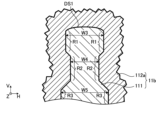
- FIG. 10 is a cross-sectional view of the anode 11b that constitutes the discharge electrode according to the first embodiment.
- FIG. 10 shows a cross section perpendicular to the Z axis of the electrode base material 111 and coating layer 112 that constitute the anode 11b.
- the cathode 11a which is not shown in FIG. 10, is located in the +V direction when viewed from the anode 11b.
- the cathode 11a is similar to that described with reference to FIG.
- Each of the two side surfaces parallel to the longitudinal direction of the electrode base material 111 includes first, second, and third regions R1, R2, and R3.
- the first, second, and third regions R1, R2, and R3 are located in this order from the one closest to the cathode 11a.
- First and second portions P1 and P2 of the coating layer 112 cover the first and second regions R1 and R2, respectively.
- the thickness T2 of the second portion P2 is larger than the thickness T1 of the first portion P1.
- the thickness T1 is 0.1 mm or more and 0.2 mm or less
- the thickness T2 is 0.05 mm or more larger than the thickness T1 and 0.5 mm or less.
- At least a portion of the surface F1 of the first portion P1 and at least a portion of the first region R1 of the side surfaces of the electrode base material 111 are parallel to each other, and at least a portion of the surface F2 of the second portion P2 is parallel to each other. and at least a portion of the second region R2 of the side surface of the electrode base material 111 are parallel to each other.
- Each part of the anode 11b has the following dimensional width.
- First width W1 of anode 11b including first portion P1 Second width W2 of anode 11b including second portion P2 Third width W3 between first regions R1 Fourth width W4 between second regions R2 Fifth width W5 between third regions R3
- the space between the first and second regions R1 and R2 is flat.
- a step is formed between the surface F1 of the first portion P1 and the surface F2 of the second portion P2, and the second width W2 is larger than the first width W1.
- the step difference between the surfaces F1 and F2 does not affect the discharge as long as the first portion P1 has a sufficient length L1 in the discharge direction, and the discharge width is determined by the first width W1.
- the space between the first and second regions R1 and R2 is not limited to being flat, and the difference between the third width W3 and the fourth width W4 is equal to the difference between the first width W1 and the second width W2. It should be smaller than the difference.
- a step is formed between the second and third regions R2 and R3, and the fifth width W5 is larger than the fourth width W4.
- the space between the surface F2 of the second portion P2 and the third region R3 is flat.
- this is not limited to the case where the space between the surface F2 and the third region R3 is flat, and the difference between the fifth width W5 and the second width W2 is the same as the difference between the first width W1 and the second width W2. It is sufficient that the difference is smaller than the difference.
- the length L2 of the second portion P2 in the discharge direction is longer than the length L1 of the first portion P1 in the discharge direction.
- the length L1 of the first portion P1 in the discharge direction is 1.5 mm or more, and is, for example, 2.0 mm.
- the length L2 of the second portion P2 in the discharge direction is 3.0 mm or more, for example, 4.0 mm.
- the discharge electrode according to the first embodiment is a discharge electrode used in a gas laser device 1 that excites a fluorine-containing laser gas by discharge, and includes a cathode 11a and an anode 11b. .
- the anode 11b is arranged to face the cathode 11a, and includes an electrode base material 111 containing metal, a coating layer 112 containing an insulating material and covering a part of the side surface parallel to the longitudinal direction of the electrode base material 111. including.
- the coating layer 112 includes a first portion P1 that covers a first region R1 of the side surface of the electrode base material 111 and a second region R2 of the side surface of the electrode base material 111 that covers the first region P1.
- the width of the discharge can be increased by suppressing the thickness of the first portion P1 of the coating layer 112 while ensuring a sufficient width of the electrode base material 111 to suppress deterioration of the electrode base material 111. Peeling can be suppressed by increasing the thickness of the second portion P2 of the coating layer 112.
- the first portion P1 of the coating layer 112 can be processed with high dimensional accuracy, for example, by thermal spraying and polishing.
- the second portion P2 of the coating layer 112 can be processed with high dimensional accuracy, for example, by thermal spraying and polishing.
- the first and second regions R1 and R2 and the first and second portions P1 and P2 are located on each of two side surfaces parallel to the longitudinal direction of the electrode base material 111. positioned.
- the third width between the first regions R1 is greater than the difference between the first width W1 of the anode 11b including the first portion P1 and the second width W2 of the anode 11b including the second portion P2.
- the difference between W3 and the fourth width W4 between the second region R2 is small. According to this, since the difference between the third width W3 and the fourth width W4 is small, processing of the electrode base material 111 can be facilitated, and the difference between the first width W1 and the second width W2 is small.
- the thicknesses T1 and T2 of the first and second portions P1 and P2 can be adjusted.
- the side surface of the electrode base material 111 includes a third region R3 located farther from the cathode 11a in the discharge direction than the second region R2, and includes the first to third regions.
- R1 to R3 and the first and second portions P1 and P2 are located on each of two side surfaces parallel to the longitudinal direction of the electrode base material 111.
- the fifth width between the third regions R3 is greater than the difference between the first width W1 of the anode 11b including the first portion P1 and the second width W2 of the anode 11b including the second portion P2.
- the difference between W5 and the second width W2 is small. According to this, since the difference between the fifth width W5 and the second width W2 is small, the second portion P2 can be processed with high dimensional accuracy using the third region R3 as a reference.
- the first region R1 and the second region R2 on the side surface of the electrode base material 111 are flat, and the surface F1 of the first portion P1 of the coating layer 112 and the second region R2 are flat.
- a step is formed between the portion P2 of the second portion and the surface F2.
- the side surface of the electrode base material 111 includes a third region R3 located farther from the cathode 11a in the discharge direction than the second region R2, and the second region R3 of the coating layer 112
- the space between the surface F2 of the portion P2 and the third region R3 of the side surface of the electrode base material 111 is flat. According to this, since the space between the surface F2 of the second portion P2 and the third region R3 is made flat, the second portion P2 can be processed with high dimensional accuracy using the third region R3 as a reference.
- the thickness T1 of the first portion P1 in the direction perpendicular to the side surface of the electrode base material 111 is 0.1 mm or more and 0.2 mm or less, and is perpendicular to the side surface of the electrode base material 111.
- the thickness T2 of the second portion P2 in the direction is 0.05 mm or more thicker than the first portion P1 and 0.5 mm or less. According to this, the thickness T1 sufficient for the first portion P1 to reinforce the electrode base material 111 can be ensured, and the discharge width can be prevented from increasing. Further, it is possible to ensure a sufficient thickness T2 to suppress peeling of the second portion P2 during manufacturing, and to suppress processing of the second portion P2 from becoming difficult.
- the length L2 of the second portion P2 in the discharge direction is longer than the length L1 of the first portion P1 in the discharge direction. According to this, peeling of the second portion P2 can be sufficiently suppressed.
- the first embodiment is similar to the comparative example.
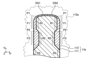
- FIG. 11 is a cross-sectional view of the anode 11b that constitutes the discharge electrode according to the second embodiment.
- FIG. 11 shows a cross section perpendicular to the Z axis of the electrode base material 111 and coating layer 112 that constitute the anode 11b.
- the cathode 11a which is not shown in FIG. 11, is located in the +V direction when viewed from the anode 11b.
- a step is formed between the first and second regions R1 and R2, a step is formed between the second and third regions R2 and R3, and a third width is formed.
- W3 is larger than the fourth width W4, and the fifth width W5 is larger than the third width W3.
- the surface F1 of the first portion P1 and the surface F2 of the second portion P2 are flat, and the surface F2 of the second portion P2 and the third region R3 is flat.
- the space between the surfaces F1 and F2 is not limited to being flat, and as long as the difference between the first width W1 and the second width W2 is smaller than the difference between the third width W3 and the fourth width W4. good. Further, the space between the surface F2 and the third region R3 is not limited to being flat, and the difference between the fifth width W5 and the second width W2 is the same as the difference between the third width W3 and the fourth width W4. It is sufficient that the difference is smaller than the difference.
- the first and second regions R1 and R2 and the first and second portions P1 and P2 are two parallel to the longitudinal direction of the electrode base material 111. Located on each side.
- the difference between the first width W1 of the anode 11b including the first portion P1 and the second width W2 of the anode 11b including the second portion P2 is the third width W3 between the first regions R1. and the fourth width W4 between the second region R2 and the second region R2. According to this, by reducing the difference between the first width W1 and the second width W2, the first and second portions P1 and P2 of the coating layer 112 can be processed with high dimensional accuracy. Further, it is possible to prevent the shapes of parts arranged around the anode 11b from becoming complicated.
- the side surface of the electrode base material 111 includes a third region R3 located farther from the cathode 11a in the discharge direction than the second region R2, and includes the first to third regions.
- R1 to R3 and the first and second portions P1 and P2 are located on each of two side surfaces parallel to the longitudinal direction of the electrode base material 111. Then, the difference between the fifth width W5 between the third region R3 and the second portion is greater than the difference between the third width W3 between the first region R1 and the fourth width W4 between the second region R2.
- the difference from the second width W2 of the anode 11b including P2 is small. According to this, since the difference between the fifth width W5 and the second width W2 is small, the second portion P2 can be processed with high dimensional accuracy using the third region R3 as a reference.
- the third width W3 between the first regions R1 is larger than the fourth width W4 between the second regions R2. According to this, it becomes easy to process the second portion P2 that covers the second region R2 to be thicker than the first portion P1 that covers the first region R1.
- the surface F1 of the first portion P1 of the coating layer 112 and the surface F2 of the second portion P2 are flat. According to this, the first and second portions P1 and P2 can be processed with high dimensional accuracy. Further, it is possible to prevent the shapes of parts arranged around the anode 11b from becoming complicated.
- the side surface of the electrode base material 111 includes a third region R3 located farther from the cathode 11a in the discharge direction than the second region R2, and a third region R3 located further from the cathode 11a in the discharge direction than the second region R2, and
- the third width W3 is larger than the fourth width W4 between the second regions R2, and the fifth width W5 between the third regions R3 is larger than the third width W3.
- the side surface of the electrode base material 111 includes a third region R3 located farther from the cathode 11a in the discharge direction than the second region R2, and the second region R3 of the coating layer 112
- the space between the surface F2 of the portion P2 and the third region R3 of the side surface of the electrode base material 111 is flat. According to this, by making the space between the surface F2 of the second portion P2 and the third region R3 flat, the second portion P2 can be processed with high dimensional accuracy using the third region R3 as a reference.
- the second embodiment is similar to the first embodiment.
- FIGS. 12 and 13 are cross-sectional views showing the manufacturing process of anode 11b constituting the discharge electrode according to the third embodiment. 12 and 13 show cross sections perpendicular to the Z axis of the electrode base material 111 and coating layers 112 and 112a that constitute the anode 11b.
- the cathode 11a which is not shown in FIGS. 12 and 13, is arranged in the +V direction when viewed from the anode 11b. In FIGS. 12 and 13, the unevenness on the surface of the coating layer 112a is exaggerated.
- the method for manufacturing the anode 11b is as follows. As shown in FIG. 12, a coating layer 112a is formed on a side surface SS1 parallel to the longitudinal direction of the electrode base material 111 constituting the anode 11b and a first discharge surface DS1 that is a surface facing the cathode 11a. .
- the coating layer 112a is formed by thermal spraying, for example.
- the sprayed film is formed to have a substantially uniform thickness along the outer shape of the electrode base material 111.
- the step of forming the coating layer 112a corresponds to the first step in the present disclosure.
- a portion of the coating layer 112a is removed by, for example, grinding or polishing the coating layer 112a so as to approximate the target shape.
- the coating layer is formed such that the second portion P2 that covers the second region R2 of the side surface SS1 is thicker than the first portion P1 that covers the first region R1 of the side surface SS1.
- 112a is removed.
- a second discharge surface DS2 is also formed.
- the step of removing part of the coating layer 112a corresponds to the second step in the present disclosure.
- the coating layer 112 having the shape described in the first embodiment is formed.
- the manufacturing method according to the third embodiment is a manufacturing method of the anode 11b of the discharge electrode used in the gas laser device 1 that excites a fluorine-containing laser gas by discharge.
- the first step is to form a coating layer 112a on the side surface parallel to the longitudinal direction of the electrode base material 111 constituting the anode 11b
- the second step is to remove a part of the coating layer 112a so as to approximate the target shape. process.
- the second step the second region R2 of the side surface of the electrode base material 111 is covered with a first portion P1 that covers the first region R1 of the side surface of the electrode base material 111.
- the coating layer 112 can be processed with high dimensional accuracy, and while ensuring a sufficient width of the electrode base material 111 to suppress deterioration of the electrode base material 111, the first portion P1 of the coating layer 112 can be By controlling the thickness, it is possible to suppress the discharge width from increasing, and by increasing the thickness of the second portion P2 of the coating layer 112, peeling during manufacturing can be suppressed.
- the second step includes forming a step between the surface F1 of the first portion P1 and the surface F2 of the second portion P2 of the coating layer 112. According to this, the thicknesses of the first and second portions P1 and P2 can be adjusted by adjusting the level difference between the surface F1 of the first portion P1 and the surface F2 of the second portion P2.
- the third embodiment is similar to the first embodiment.
- FIGS. 14 and 15 are cross-sectional views showing the manufacturing process of anode 11b constituting the discharge electrode according to the fourth embodiment. 14 and 15 show cross sections perpendicular to the Z axis of the electrode base material 111 and coating layers 112 and 112a that constitute the anode 11b.
- the cathode 11a which is not shown in FIGS. 14 and 15, is arranged in the +V direction when viewed from the anode 11b. In FIGS. 14 and 15, the unevenness on the surface of the coating layer 112a is exaggerated.
- the method for manufacturing the anode 11b is as follows. As shown in FIG. 14, the fourth width W4 between the second regions R2 is smaller than the third width W3 between the first regions R1 of the electrode base material 111 constituting the anode 11b.
- the electrode base material 111 is processed.
- the step of processing the electrode base material 111 corresponds to the third step in the present disclosure.
- a coating layer 112a is formed on the first to third regions R1 to R3 on the side surface of the electrode base material 111 and the first discharge surface DS1, which is the surface facing the cathode 11a.
- the coating layer 112a is formed by thermal spraying, for example.
- the sprayed film is formed to have a substantially uniform thickness along the outer shape of the electrode base material 111.
- the step of forming the coating layer 112a corresponds to the first step in the present disclosure.
- a portion of the coating layer 112a is removed by, for example, grinding or polishing the coating layer 112a so as to approximate the target shape. This reduces the level difference between the surface F1 of the first portion P1 and the surface F2 of the second portion P2.
- a second discharge surface DS2 is also formed.
- the step of removing part of the coating layer 112a corresponds to the second step in the present disclosure. As a result, the coating layer 112 having the shape described in the second embodiment is formed.
- the first and second regions R1 and R2 are located on each of two side surfaces parallel to the longitudinal direction of the electrode base material 111.
- the electrode base material 111 is adjusted so that the fourth width W4 between the second regions R2 is smaller than the third width W3 between the first regions R1.
- the second step includes reducing the level difference between the surface F1 of the first portion P1 and the surface F2 of the second portion P2 of the coating layer 112. According to this, the first and second portions P1 and P2 can be processed with high dimensional accuracy. In other respects, the fourth embodiment is similar to the second embodiment.
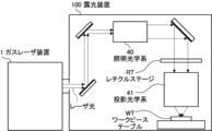
- FIG. 16 schematically shows the configuration of an exposure apparatus 100 connected to the gas laser apparatus 1.
- Gas laser device 1 generates laser light and outputs it to exposure device 100 .
- exposure apparatus 100 includes an illumination optical system 40 and a projection optical system 41.
- the illumination optical system 40 illuminates a reticle pattern of a reticle (not shown) placed on the reticle stage RT with laser light incident from the gas laser device 1.
- the projection optical system 41 reduces and projects the laser beam that has passed through the reticle, and forms an image on a workpiece (not shown) placed on the workpiece table WT.
- the workpiece is a photosensitive substrate, such as a semiconductor wafer, coated with photoresist.
- Exposure apparatus 100 exposes a workpiece to laser light that reflects a reticle pattern by synchronously moving reticle stage RT and workpiece table WT in parallel. After a reticle pattern is transferred to a semiconductor wafer through the exposure process described above, electronic devices can be manufactured through a plurality of steps.
Landscapes
- Physics & Mathematics (AREA)
- Electromagnetism (AREA)
- Engineering & Computer Science (AREA)
- Plasma & Fusion (AREA)
- Optics & Photonics (AREA)
- Lasers (AREA)
Abstract
Description
1.比較例
1.1 ガスレーザ装置1の構成
1.2 動作
1.3 比較例の課題
2.コーティング層112に段差を設けたアノード11b
2.1 構成
2.2 作用
3.電極基材111に段差を設けたアノード11b
3.1 構成
3.2 作用
4.コーティング層112に段差を設けたアノード11bの製造方法
4.1 製造工程
4.2 作用
5.電極基材111に段差を設けたアノード11bの製造方法
5.1 製造工程
5.2 作用
6.その他
1.1 ガスレーザ装置1の構成
図1は、比較例に係るガスレーザ装置1の構成を模式的に示す。図1に示されるガスレーザ装置1は、レーザチャンバ10と、一対の放電電極を構成するカソード11a及びアノード11bと、充電器12と、パルスパワーモジュール(PPM)13と、狭帯域化モジュール14と、出力結合ミラー15と、レーザコントローラ30と、を含む。狭帯域化モジュール14と出力結合ミラー15とが、光共振器を構成する。レーザチャンバ10は、光共振器の光路に配置されている。図1においては、カソード11a及びアノード11bの間の放電方向に略垂直で、且つ、出力結合ミラー15から出力されるレーザ光の進行方向に略垂直な方向から見たレーザチャンバ10の内部構成が示されている。
レーザコントローラ30は、露光装置100(図16参照)から、目標パルスエネルギーの設定データと、発光トリガ信号と、を受信する。レーザコントローラ30は、目標パルスエネルギーの設定データに基づいて、充電器12に充電電圧の設定データを送信する。また、レーザコントローラ30は、発光トリガ信号に基づいて、パルスパワーモジュール13にトリガ信号を送信する。
プリズム14aからグレーティング14bに入射した光は、グレーティング14bの複数の溝によって反射されるとともに、光の波長に応じた方向に回折させられる。
出力結合ミラー15は、レーザチャンバ10のウインドウ10bから出射した光のうちの一部を透過させて出力し、他の一部を反射させてレーザチャンバ10内に戻す。
図4は、長期にわたって使用されたアノード11bの断面図である。アノード11bを長期にわたって使用すると、第1の放電面DS1の付近から電極基材111が劣化することがある。例えば、電極基材111の一部がレーザガスに含まれるフッ素と反応し、脆化することがある。コーティング層112のうち、特に側面SS1を被覆する部分には、電極基材111の脆化部分111aを補強しアノード11bの強度を保つ機能が求められる。
コーティング層112は、電極基材111の表面が劣化することを抑制するために絶縁材料を含み、コーティング層112を構成する材料の抵抗率は電極基材111を構成する材料の抵抗率よりも高くなっている。しかし、コーティング層112の電気抵抗が高すぎると放電しにくくなるため、コーティング層112には絶縁材料の他に金属も含まれている。また、カソード11a及びアノード11bの間に高電圧が印加されたとき、アノード11bの角部の付近に電界が集中しやすい。このため、放電空間50はコーティング層112の角部の付近にも及ぶ。
図7においては、放電によるカソード11aからアノード11bへの電子の流れが放電生成物51に引き寄せられる。このため、図7における放電空間50は+H方向に偏って形成され、放電が不安定となり、レーザ光の生成が不安定となる。
一方、図8のように、放電生成物51がカソード11a及びアノード11bから遠くに位置していれば、放電空間50は放電生成物51の影響をあまり受けずに、図5における放電空間50と同様に形成される。
(1)クロスフローファン21によるレーザガスの流速を大きくする
(2)放電空間50のH軸方向の幅を小さくする
また、放電空間50のH軸方向の幅を小さくするために、電極基材111の幅を狭くすることが考えられるが、電極基材111の幅を狭くすると、電極基材111の中心まで早期に劣化が進行し、寿命が短くなってしまう場合がある。
そこで、放電空間50のH軸方向の幅を小さくするために、コーティング層112のうちの側面SS1を被覆する部分の厚みT0(図4参照)は最小限とすることが望ましい。
2.1 構成
図10は、第1の実施形態に係る放電電極を構成するアノード11bの断面図である。図10は、アノード11bを構成する電極基材111及びコーティング層112のZ軸に垂直な断面を示す。図10には図示されていないカソード11aは、アノード11bから見て+V方向に位置する。カソード11aは図3を参照しながら説明したものと同様である。
第1の部分P1を含むアノード11bの第1の幅W1
第2の部分P2を含むアノード11bの第2の幅W2
第1の領域R1間の第3の幅W3
第2の領域R2間の第4の幅W4
第3の領域R3間の第5の幅W5
但し、第1及び第2の領域R1及びR2の間は平坦である場合に限られず、第3の幅W3と第4の幅W4との差が、第1の幅W1と第2の幅W2との差より小さければよい。
但し、表面F2と第3の領域R3との間が平坦である場合に限られず、第5の幅W5と第2の幅W2との差が、第1の幅W1と第2の幅W2との差より小さければよい。
(1)第1の実施形態に係る放電電極は、フッ素を含むレーザガスを放電により励起するガスレーザ装置1に使用される放電電極であって、カソード11aと、アノード11bと、を備える。アノード11bは、カソード11aと対向して配置され、金属を含む電極基材111と、電極基材111の長手方向に平行な側面の一部を被覆しており絶縁材料を含むコーティング層112と、を含む。コーティング層112は、電極基材111の側面のうちの第1の領域R1を被覆する第1の部分P1と、電極基材111の側面のうちの第2の領域R2であって第1の領域R1よりも長手方向に垂直な放電方向においてカソード11aから遠くに位置する第2の領域R2を被覆し、第1の部分P1よりも厚い第2の部分P2と、を含む。
これによれば、電極基材111の劣化を抑制するために電極基材111の幅を十分に確保しつつ、コーティング層112の第1の部分P1の厚みを抑制することで放電幅が大きくなることを抑制し、コーティング層112の第2の部分P2を厚くすることで剥離を抑制し得る。
これによれば、例えば溶射及び研磨により、コーティング層112の第1の部分P1を高い寸法精度で加工できる。
これによれば、例えば溶射及び研磨により、コーティング層112の第2の部分P2を高い寸法精度で加工できる。
これによれば、第3の幅W3と第4の幅W4との差が小さいので電極基材111の加工を容易にすることができ、第1の幅W1と第2の幅W2との差を調整することで第1及び第2の部分P1及びP2の厚さT1及びT2を調整できる。
これによれば、第5の幅W5と第2の幅W2との差が小さいので第3の領域R3を基準として第2の部分P2を高い寸法精度で加工できる。
これによれば、第1の領域R1と第2の領域R2との間を平坦とするので電極基材111の加工を容易にすることができ、第1の部分P1の表面F1と第2の部分P2の表面F2との段差を調整することで第1及び第2の部分P1及びP2の厚さT1及びT2を調整できる。
これによれば、第2の部分P2の表面F2と第3の領域R3との間を平坦とするので、第3の領域R3を基準として第2の部分P2を高い寸法精度で加工できる。
これによれば、第1の部分P1が電極基材111を補強するのに十分な厚さT1を確保するとともに、放電幅が大きくなることを抑制し得る。また、製造時における第2の部分P2の剥離を抑制するのに十分な厚さT2を確保するとともに、第2の部分P2の加工が難しくなることを抑制し得る。
これによれば、第2の部分P2の剥離を十分に抑制し得る。
その他の点については、第1の実施形態は比較例と同様である。
3.1 構成
図11は、第2の実施形態に係る放電電極を構成するアノード11bの断面図である。図11は、アノード11bを構成する電極基材111及びコーティング層112のZ軸に垂直な断面を示す。図11には図示されていないカソード11aは、アノード11bから見て+V方向に位置する。
(10)第2の実施形態において、第1及び第2の領域R1及びR2と第1及び第2の部分P1及びP2とは、電極基材111の長手方向に平行な2つの側面の各々に位置している。そして、第1の部分P1を含むアノード11bの第1の幅W1と第2の部分P2を含むアノード11bの第2の幅W2との差は、第1の領域R1間の第3の幅W3と第2の領域R2間の第4の幅W4との差より小さい。
これによれば、第1の幅W1と第2の幅W2との差を小さくすることで、コーティング層112の第1及び第2の部分P1及びP2を高い寸法精度で加工し得る。また、アノード11bの周辺に配置される部品形状が複雑になることを抑制し得る。
これによれば、第5の幅W5と第2の幅W2との差が小さいので第3の領域R3を基準として第2の部分P2を高い寸法精度で加工できる。
これによれば、第2の領域R2を被覆する第2の部分P2を、第1の領域R1を被覆する第1の部分P1よりも厚く加工することが容易になる。
これによれば、第1及び第2の部分P1及びP2を高い寸法精度で加工し得る。また、アノード11bの周辺に配置される部品形状が複雑になることを抑制し得る。
これによれば、第3の領域R3を基準として第1及び第2の部分P1及びP2を加工することで、第2の領域R2を被覆する第2の部分P2を、第1の領域R1を被覆する第1の部分P1よりも厚く加工することが容易になる。
これによれば、第2の部分P2の表面F2と第3の領域R3との間を平坦とすることで、第3の領域R3を基準として第2の部分P2を高い寸法精度で加工できる。
その他の点については、第2の実施形態は第1の実施形態と同様である。
4.1 製造工程
図12及び図13は、第3の実施形態に係る放電電極を構成するアノード11bの製造工程を示す断面図である。図12及び図13は、アノード11bを構成する電極基材111及びコーティング層112及び112aのZ軸に垂直な断面を示す。図12及び図13には図示されていないカソード11aは、アノード11bから見て+V方向に配置される。図12及び図13においてはコーティング層112aの表面の凹凸が誇張して描かれている。
図12に示されるように、アノード11bを構成する電極基材111の長手方向に平行な側面SS1と、カソード11aと対向する面となる第1の放電面DS1と、にコーティング層112aを形成する。コーティング層112aは例えば溶射により形成される。溶射膜は電極基材111の外形に沿ってほぼ一様の厚みに形成される。コーティング層112aを形成する工程は本開示における第1の工程に相当する。
これにより、第1の実施形態において説明した形状のコーティング層112が形成される。
(16)第3の実施形態に係る製造方法は、フッ素を含むレーザガスを放電により励起するガスレーザ装置1においてカソード11aと対向した配置で使用される放電電極のアノード11bの製造方法であって、アノード11bを構成する電極基材111の長手方向に平行な側面にコーティング層112aを形成する第1の工程と、目標形状に近づくようにコーティング層112aの一部を除去する第2の工程と、を含む。第2の工程は、電極基材111の側面のうちの第1の領域R1を被覆する第1の部分P1よりも、電極基材111の側面のうちの第2の領域R2であって第1の領域R1よりも長手方向に垂直な放電方向においてカソード11aから遠くに位置する第2の領域R2を被覆する第2の部分P2が厚くなるようにコーティング層112aの一部を除去することを含む。
これによれば、コーティング層112を高い寸法精度で加工でき、電極基材111の劣化を抑制するために電極基材111の幅を十分に確保しつつ、コーティング層112の第1の部分P1の厚みを抑制することで放電幅が大きくなることを抑制し、コーティング層112の第2の部分P2を厚くすることで製造時の剥離を抑制し得る。
これによれば、第1の部分P1の表面F1と第2の部分P2の表面F2との段差を調整することで第1及び第2の部分P1及びP2の厚さを調整できる。
その他の点については、第3の実施形態は第1の実施形態と同様である。
5.1 製造工程
図14及び図15は、第4の実施形態に係る放電電極を構成するアノード11bの製造工程を示す断面図である。図14及び図15は、アノード11bを構成する電極基材111及びコーティング層112及び112aのZ軸に垂直な断面を示す。図14及び図15には図示されていないカソード11aは、アノード11bから見て+V方向に配置される。図14及び図15においてはコーティング層112aの表面の凹凸が誇張して描かれている。
図14に示されるように、すなわちアノード11bを構成する電極基材111の第1の領域R1間の第3の幅W3よりも第2の領域R2間の第4の幅W4が小さくなるように電極基材111を加工する。電極基材111を加工する工程は本開示における第3の工程に相当する。
次に、電極基材111の側面の第1~第3の領域R1~R3と、カソード11aと対向する面となる第1の放電面DS1と、にコーティング層112aを形成する。コーティング層112aは例えば溶射により形成される。溶射膜は電極基材111の外形に沿ってほぼ一様の厚みに形成される。コーティング層112aを形成する工程は本開示における第1の工程に相当する。
これにより、第2の実施形態において説明した形状のコーティング層112が形成される。
(18)第4の実施形態において、第1及び第2の領域R1及びR2は、電極基材111の長手方向に平行な2つの側面の各々に位置している。アノード11bの製造方法は、第1の工程の前に、第1の領域R1間の第3の幅W3よりも第2の領域R2間の第4の幅W4が小さくなるように電極基材111を加工する第3の工程を含む。
これによれば、第2の領域R2を被覆する第2の部分P2を、第1の領域R1を被覆する第1の部分P1よりも厚く加工することが容易になる。
これによれば、第1及び第2の部分P1及びP2を高い寸法精度で加工し得る。
その他の点については、第4の実施形態は第2の実施形態と同様である。
図16は、ガスレーザ装置1に接続された露光装置100の構成を概略的に示す。ガスレーザ装置1はレーザ光を生成して露光装置100に出力する。
図16において、露光装置100は、照明光学系40と投影光学系41とを含む。照明光学系40は、ガスレーザ装置1から入射したレーザ光によって、レチクルステージRT上に配置された図示しないレチクルのレチクルパターンを照明する。投影光学系41は、レチクルを透過したレーザ光を、縮小投影してワークピーステーブルWT上に配置された図示しないワークピースに結像させる。ワークピースはフォトレジストが塗布された半導体ウエハ等の感光基板である。露光装置100は、レチクルステージRTとワークピーステーブルWTとを同期して平行移動させることにより、レチクルパターンを反映したレーザ光をワークピースに露光する。以上のような露光工程によって半導体ウエハにレチクルパターンを転写後、複数の工程を経ることで電子デバイスを製造することができる。
Claims (20)
- フッ素を含むレーザガスを放電により励起するガスレーザ装置に使用される放電電極であって、
カソードと、
アノードと、
を備え、
前記アノードは、
前記カソードと対向して配置され、
金属を含む電極基材と、前記電極基材の長手方向に平行な側面の一部を被覆しており絶縁材料を含むコーティング層と、を含み、
前記コーティング層は、
前記側面のうちの第1の領域を被覆する第1の部分と、
前記側面のうちの第2の領域であって前記第1の領域よりも前記長手方向に垂直な放電方向において前記カソードから遠くに位置する前記第2の領域を被覆し、前記第1の部分よりも厚い第2の部分と、を含む、
放電電極。 - 請求項1に記載の放電電極であって、
前記コーティング層の前記第1の部分の表面の少なくとも一部と、前記側面のうちの前記第1の領域の少なくとも一部と、が平行である、
放電電極。 - 請求項1に記載の放電電極であって、
前記コーティング層の前記第2の部分の表面の少なくとも一部と、前記側面のうちの前記第2の領域の少なくとも一部と、が平行である、
放電電極。 - 請求項1に記載の放電電極であって、
前記第1及び第2の領域と前記第1及び第2の部分とは、前記側面を含む前記長手方向に平行な2つの側面の各々に位置しており、
前記第1の部分を含む前記アノードの第1の幅と前記第2の部分を含む前記アノードの第2の幅との差よりも、前記第1の領域間の第3の幅と前記第2の領域間の第4の幅との差が小さい、
放電電極。 - 請求項1に記載の放電電極であって、
前記側面は、前記第2の領域よりも前記放電方向において前記カソードから遠くに位置する第3の領域を含み、
前記第1~第3の領域と前記第1及び第2の部分とは、前記側面を含む前記長手方向に平行な2つの側面の各々に位置しており、
前記第1の部分を含む前記アノードの第1の幅と前記第2の部分を含む前記アノードの第2の幅との差よりも、前記第3の領域間の第5の幅と前記第2の幅との差が小さい、
放電電極。 - 請求項1に記載の放電電極であって、
前記側面の前記第1の領域と前記第2の領域との間は平坦であり、
前記コーティング層の前記第1の部分の表面と前記第2の部分の表面との間に段差が形成された、
放電電極。 - 請求項6に記載の放電電極であって、
前記側面は、前記第2の領域よりも前記放電方向において前記カソードから遠くに位置する第3の領域を含み、
前記コーティング層の前記第2の部分の表面と、前記側面のうちの前記第3の領域との間は平坦である、
放電電極。 - 請求項1に記載の放電電極であって、
前記側面に垂直な方向における前記第1の部分の厚さは0.1mm以上0.2mm以下であり、
前記側面に垂直な方向における前記第2の部分の厚さは、前記第1の部分よりも0.05mm以上厚く、且つ0.5mm以下である、
放電電極。 - 請求項1に記載の放電電極であって、
前記第1の部分の前記放電方向の長さより、前記第2の部分の前記放電方向の長さが長い、
放電電極。 - 請求項1に記載の放電電極であって、
前記第1及び第2の領域と前記第1及び第2の部分とは、前記側面を含む前記長手方向に平行な2つの側面の各々に位置しており、
前記第1の部分を含む前記アノードの第1の幅と前記第2の部分を含む前記アノードの第2の幅との差は、前記第1の領域間の第3の幅と前記第2の領域間の第4の幅との差より小さい、
放電電極。 - 請求項1に記載の放電電極であって、
前記側面は、前記第2の領域よりも前記放電方向において前記カソードから遠くに位置する第3の領域を含み、
前記第1~第3の領域と前記第1及び第2の部分とは、前記側面を含む前記長手方向に平行な2つの側面の各々に位置しており、
前記第1の領域間の第3の幅と前記第2の領域間の第4の幅との差よりも、前記第3の領域間の第5の幅と前記第2の部分を含む前記アノードの第2の幅との差が小さい、
放電電極。 - 請求項1に記載の放電電極であって、
前記第1の領域間の第3の幅が、前記第2の領域間の第4の幅よりも大きい、
放電電極。 - 請求項12に記載の放電電極であって、
前記コーティング層の前記第1の部分の表面と前記第2の部分の表面との間は平坦である、
放電電極。 - 請求項12に記載の放電電極であって、
前記側面は、前記第2の領域よりも前記放電方向において前記カソードから遠くに位置する第3の領域を含み、
前記第3の領域間の第5の幅が、前記第3の幅よりも大きい、
放電電極。 - 請求項12に記載の放電電極であって、
前記側面は、前記第2の領域よりも前記放電方向において前記カソードから遠くに位置する第3の領域を含み、
前記コーティング層の前記第2の部分の表面と、前記側面のうちの前記第3の領域との間は平坦である、
放電電極。 - フッ素を含むレーザガスを放電により励起するガスレーザ装置においてカソードと対向した配置で使用される放電電極のアノードの製造方法であって、
前記アノードを構成する電極基材の長手方向に平行な側面にコーティング層を形成する第1の工程と、
目標形状に近づくように前記コーティング層の一部を除去する第2の工程と、
を含み、
前記第2の工程は、前記側面のうちの第1の領域を被覆する第1の部分よりも、前記側面のうちの第2の領域であって前記第1の領域よりも前記長手方向に垂直な放電方向において前記カソードから遠くに位置する前記第2の領域を被覆する第2の部分が厚くなるように前記コーティング層の一部を除去することを含む、製造方法。 - 請求項16に記載の製造方法であって、
前記第2の工程は、前記コーティング層の前記第1の部分の表面と前記第2の部分の表面との間に段差を形成することを含む、
製造方法。 - 請求項16に記載の製造方法であって、
前記第1及び第2の領域は、前記側面を含む前記長手方向に平行な2つの側面の各々に位置しており、
前記第1の工程の前に、前記第1の領域間の第3の幅よりも前記第2の領域間の第4の幅が小さくなるように前記電極基材を加工する第3の工程
をさらに含む、製造方法。 - 請求項18に記載の製造方法であって、
前記第2の工程は、前記コーティング層の前記第1の部分の表面と前記第2の部分の表面との間の段差を低減することを含む、
製造方法。 - 電子デバイスの製造方法であって、
フッ素を含むレーザガスを放電により励起するガスレーザ装置に使用される放電電極であって、
カソードと、
アノードと、
を備え、
前記アノードは、
前記カソードと対向して配置され、
金属を含む電極基材と、前記電極基材の長手方向に平行な側面の一部を被覆しており絶縁材料を含むコーティング層と、を含み、
前記コーティング層は、
前記側面のうちの第1の領域を被覆する第1の部分と、
前記側面のうちの第2の領域であって前記第1の領域よりも前記長手方向に垂直な放電方向において前記カソードから遠くに位置する前記第2の領域を被覆し、前記第1の部分よりも厚い第2の部分と、を含む、
前記放電電極
を備えたレーザチャンバを含むガスレーザ装置によってレーザ光を生成し、
前記レーザ光を露光装置に出力し、
電子デバイスを製造するために、前記露光装置内で感光基板上に前記レーザ光を露光する
ことを含む電子デバイスの製造方法。
Priority Applications (4)
| Application Number | Priority Date | Filing Date | Title |
|---|---|---|---|
| CN202280094605.4A CN119256456A (zh) | 2022-05-11 | 2022-05-11 | 放电电极、阳极的制造方法以及电子器件的制造方法 |
| PCT/JP2022/019914 WO2023218548A1 (ja) | 2022-05-11 | 2022-05-11 | 放電電極、アノードの製造方法、及び電子デバイスの製造方法 |
| JP2024520135A JPWO2023218548A1 (ja) | 2022-05-11 | 2022-05-11 | |
| US18/912,020 US20250038469A1 (en) | 2022-05-11 | 2024-10-10 | Discharge electrodes, manufacturing method of anode, and electronic device manufacturing method |
Applications Claiming Priority (1)
| Application Number | Priority Date | Filing Date | Title |
|---|---|---|---|
| PCT/JP2022/019914 WO2023218548A1 (ja) | 2022-05-11 | 2022-05-11 | 放電電極、アノードの製造方法、及び電子デバイスの製造方法 |
Related Child Applications (1)
| Application Number | Title | Priority Date | Filing Date |
|---|---|---|---|
| US18/912,020 Continuation US20250038469A1 (en) | 2022-05-11 | 2024-10-10 | Discharge electrodes, manufacturing method of anode, and electronic device manufacturing method |
Publications (1)
| Publication Number | Publication Date |
|---|---|
| WO2023218548A1 true WO2023218548A1 (ja) | 2023-11-16 |
Family
ID=88729974
Family Applications (1)
| Application Number | Title | Priority Date | Filing Date |
|---|---|---|---|
| PCT/JP2022/019914 Ceased WO2023218548A1 (ja) | 2022-05-11 | 2022-05-11 | 放電電極、アノードの製造方法、及び電子デバイスの製造方法 |
Country Status (4)
| Country | Link |
|---|---|
| US (1) | US20250038469A1 (ja) |
| JP (1) | JPWO2023218548A1 (ja) |
| CN (1) | CN119256456A (ja) |
| WO (1) | WO2023218548A1 (ja) |
Citations (6)
| Publication number | Priority date | Publication date | Assignee | Title |
|---|---|---|---|---|
| JP2003152249A (ja) * | 2001-08-27 | 2003-05-23 | Komatsu Ltd | 放電電極及び放電電極の製造方法 |
| JP2004179272A (ja) * | 2002-11-26 | 2004-06-24 | Komatsu Ltd | レーザ装置用主放電電極及びその製造方法 |
| US20070002918A1 (en) * | 2005-06-30 | 2007-01-04 | Norbert Niemoeller | Acoustic shock-wave damping in pulsed gas-laser discharge |
| JP2007500942A (ja) * | 2003-07-29 | 2007-01-18 | サイマー インコーポレイテッド | ハロゲンガス放電レーザ電極 |
| JP2009200520A (ja) * | 2000-03-15 | 2009-09-03 | Komatsu Ltd | ガスレーザ用電極、その電極を用いたレーザチャンバ及びガスレーザ装置 |
| US20100239748A1 (en) * | 2007-02-27 | 2010-09-23 | Coherent, Inc. | Electrodes for generating a stable discharge in gas laser systems |
-
2022
- 2022-05-11 JP JP2024520135A patent/JPWO2023218548A1/ja active Pending
- 2022-05-11 CN CN202280094605.4A patent/CN119256456A/zh active Pending
- 2022-05-11 WO PCT/JP2022/019914 patent/WO2023218548A1/ja not_active Ceased
-
2024
- 2024-10-10 US US18/912,020 patent/US20250038469A1/en active Pending
Patent Citations (6)
| Publication number | Priority date | Publication date | Assignee | Title |
|---|---|---|---|---|
| JP2009200520A (ja) * | 2000-03-15 | 2009-09-03 | Komatsu Ltd | ガスレーザ用電極、その電極を用いたレーザチャンバ及びガスレーザ装置 |
| JP2003152249A (ja) * | 2001-08-27 | 2003-05-23 | Komatsu Ltd | 放電電極及び放電電極の製造方法 |
| JP2004179272A (ja) * | 2002-11-26 | 2004-06-24 | Komatsu Ltd | レーザ装置用主放電電極及びその製造方法 |
| JP2007500942A (ja) * | 2003-07-29 | 2007-01-18 | サイマー インコーポレイテッド | ハロゲンガス放電レーザ電極 |
| US20070002918A1 (en) * | 2005-06-30 | 2007-01-04 | Norbert Niemoeller | Acoustic shock-wave damping in pulsed gas-laser discharge |
| US20100239748A1 (en) * | 2007-02-27 | 2010-09-23 | Coherent, Inc. | Electrodes for generating a stable discharge in gas laser systems |
Also Published As
| Publication number | Publication date |
|---|---|
| US20250038469A1 (en) | 2025-01-30 |
| JPWO2023218548A1 (ja) | 2023-11-16 |
| CN119256456A (zh) | 2025-01-03 |
Similar Documents
| Publication | Publication Date | Title |
|---|---|---|
| US12347995B2 (en) | Chamber device, gas laser device, and electronic device manufacturing method | |
| JP2631607B2 (ja) | レーザ装置 | |
| US20240405497A1 (en) | Chamber of gas laser apparatus and electronic device manufacturing method | |
| JP6701198B2 (ja) | レーザチャンバ | |
| WO2023218548A1 (ja) | 放電電極、アノードの製造方法、及び電子デバイスの製造方法 | |
| JP7547508B2 (ja) | 放電電極、アノードの製造方法、及び電子デバイスの製造方法 | |
| US20230108886A1 (en) | Gas laser apparatus and electronic device manufacturing method | |
| CN113287235B (zh) | 激光用腔装置、气体激光装置和电子器件的制造方法 | |
| WO2023170835A1 (ja) | ガスレーザ装置のチャンバのベーキング方法及び電子デバイスの製造方法 | |
| JP7813870B2 (ja) | 放電電極、放電電極の製造方法、及び電子デバイスの製造方法 | |
| US20250233379A1 (en) | Discharge electrode, manufacturing method for discharge electrode, and manufacturing method for electronic device | |
| US20250300418A1 (en) | Discharge chamber for gas laser apparatus and electronic device manufacturing method | |
| US20250233378A1 (en) | Chamber of gas laser apparatus, gas laser apparatus, and electronic device manufacturing method | |
| WO2023127286A1 (ja) | ガスレーザ装置及び電子デバイスの製造方法 | |
| US20240405496A1 (en) | Chamber for gas laser device, gas laser device, and electronic device manufacturing method | |
| US20250210927A1 (en) | Laser chamber, gas laser apparatus, and method for manufacturing electronic devices | |
| US20250329978A1 (en) | Chamber apparatus for laser, gas laser apparatus, and electronic device manufacturing method | |
| US20250337210A1 (en) | Chamber device of gas laser apparatus, gas laser apparatus, and electronic device manufacturing method | |
| US20250266654A1 (en) | Gas laser device and electronic device manufacturing method | |
| US12327975B2 (en) | Chamber device, and electronic device manufacturing method | |
| WO2023181207A1 (ja) | ガスレーザ装置及び電子デバイスの製造方法 | |
| JP2025166389A (ja) | レーザチャンバ、放電電極、及び電子デバイスの製造方法 | |
| JP2025149472A (ja) | チャンバ装置、ガスレーザ装置、及び電子デバイスの製造方法 | |
| KR20250167597A (ko) | 레이저 챔버 내에서 음향 제어를 위한 장치 및 방법 | |
| JP2025142837A (ja) | レーザ用チャンバ装置、ガスレーザ装置、及び電子デバイスの製造方法 |
Legal Events
| Date | Code | Title | Description |
|---|---|---|---|
| 121 | Ep: the epo has been informed by wipo that ep was designated in this application |
Ref document number: 22941629 Country of ref document: EP Kind code of ref document: A1 |
|
| WWE | Wipo information: entry into national phase |
Ref document number: 202280094605.4 Country of ref document: CN |
|
| WWE | Wipo information: entry into national phase |
Ref document number: 2024520135 Country of ref document: JP |
|
| NENP | Non-entry into the national phase |
Ref country code: DE |
|
| WWP | Wipo information: published in national office |
Ref document number: 202280094605.4 Country of ref document: CN |
|
| 122 | Ep: pct application non-entry in european phase |
Ref document number: 22941629 Country of ref document: EP Kind code of ref document: A1 |