WO2023199152A1 - 有機化合物、発光デバイス、表示装置 - Google Patents
有機化合物、発光デバイス、表示装置 Download PDFInfo
- Publication number
- WO2023199152A1 WO2023199152A1 PCT/IB2023/053221 IB2023053221W WO2023199152A1 WO 2023199152 A1 WO2023199152 A1 WO 2023199152A1 IB 2023053221 W IB2023053221 W IB 2023053221W WO 2023199152 A1 WO2023199152 A1 WO 2023199152A1
- Authority
- WO
- WIPO (PCT)
- Prior art keywords
- layer
- electrode
- emitting device
- light emitting
- carbon atoms
- Prior art date
- Legal status (The legal status is an assumption and is not a legal conclusion. Google has not performed a legal analysis and makes no representation as to the accuracy of the status listed.)
- Ceased
Links
Images


























Classifications
-
- C—CHEMISTRY; METALLURGY
- C09—DYES; PAINTS; POLISHES; NATURAL RESINS; ADHESIVES; COMPOSITIONS NOT OTHERWISE PROVIDED FOR; APPLICATIONS OF MATERIALS NOT OTHERWISE PROVIDED FOR
- C09K—MATERIALS FOR MISCELLANEOUS APPLICATIONS, NOT PROVIDED FOR ELSEWHERE
- C09K11/00—Luminescent materials, e.g. electroluminescent or chemiluminescent
- C09K11/06—Luminescent materials, e.g. electroluminescent or chemiluminescent containing organic luminescent materials
-
- C—CHEMISTRY; METALLURGY
- C07—ORGANIC CHEMISTRY
- C07F—ACYCLIC, CARBOCYCLIC OR HETEROCYCLIC COMPOUNDS CONTAINING ELEMENTS OTHER THAN CARBON, HYDROGEN, HALOGEN, OXYGEN, NITROGEN, SULFUR, SELENIUM OR TELLURIUM
- C07F15/00—Compounds containing elements of Groups 8, 9, 10 or 18 of the Periodic Table
-
- C—CHEMISTRY; METALLURGY
- C07—ORGANIC CHEMISTRY
- C07F—ACYCLIC, CARBOCYCLIC OR HETEROCYCLIC COMPOUNDS CONTAINING ELEMENTS OTHER THAN CARBON, HYDROGEN, HALOGEN, OXYGEN, NITROGEN, SULFUR, SELENIUM OR TELLURIUM
- C07F15/00—Compounds containing elements of Groups 8, 9, 10 or 18 of the Periodic Table
- C07F15/0006—Compounds containing elements of Groups 8, 9, 10 or 18 of the Periodic Table compounds of the platinum group
- C07F15/0033—Iridium compounds
-
- H—ELECTRICITY
- H05—ELECTRIC TECHNIQUES NOT OTHERWISE PROVIDED FOR
- H05B—ELECTRIC HEATING; ELECTRIC LIGHT SOURCES NOT OTHERWISE PROVIDED FOR; CIRCUIT ARRANGEMENTS FOR ELECTRIC LIGHT SOURCES, IN GENERAL
- H05B33/00—Electroluminescent light sources
- H05B33/12—Light sources with substantially two-dimensional [2D] radiating surfaces
-
- H—ELECTRICITY
- H10—SEMICONDUCTOR DEVICES; ELECTRIC SOLID-STATE DEVICES NOT OTHERWISE PROVIDED FOR
- H10K—ORGANIC ELECTRIC SOLID-STATE DEVICES
- H10K50/00—Organic light-emitting devices
-
- H—ELECTRICITY
- H10—SEMICONDUCTOR DEVICES; ELECTRIC SOLID-STATE DEVICES NOT OTHERWISE PROVIDED FOR
- H10K—ORGANIC ELECTRIC SOLID-STATE DEVICES
- H10K50/00—Organic light-emitting devices
- H10K50/10—OLEDs or polymer light-emitting diodes [PLED]
- H10K50/14—Carrier transporting layers
- H10K50/15—Hole transporting layers
-
- H—ELECTRICITY
- H10—SEMICONDUCTOR DEVICES; ELECTRIC SOLID-STATE DEVICES NOT OTHERWISE PROVIDED FOR
- H10K—ORGANIC ELECTRIC SOLID-STATE DEVICES
- H10K50/00—Organic light-emitting devices
- H10K50/80—Constructional details
- H10K50/805—Electrodes
-
- H—ELECTRICITY
- H10—SEMICONDUCTOR DEVICES; ELECTRIC SOLID-STATE DEVICES NOT OTHERWISE PROVIDED FOR
- H10K—ORGANIC ELECTRIC SOLID-STATE DEVICES
- H10K59/00—Integrated devices, or assemblies of multiple devices, comprising at least one organic light-emitting element covered by group H10K50/00
-
- H—ELECTRICITY
- H10—SEMICONDUCTOR DEVICES; ELECTRIC SOLID-STATE DEVICES NOT OTHERWISE PROVIDED FOR
- H10K—ORGANIC ELECTRIC SOLID-STATE DEVICES
- H10K59/00—Integrated devices, or assemblies of multiple devices, comprising at least one organic light-emitting element covered by group H10K50/00
- H10K59/10—OLED displays
- H10K59/12—Active-matrix OLED [AMOLED] displays
- H10K59/121—Active-matrix OLED [AMOLED] displays characterised by the geometry or disposition of pixel elements
- H10K59/1213—Active-matrix OLED [AMOLED] displays characterised by the geometry or disposition of pixel elements the pixel elements being TFTs
-
- H—ELECTRICITY
- H10—SEMICONDUCTOR DEVICES; ELECTRIC SOLID-STATE DEVICES NOT OTHERWISE PROVIDED FOR
- H10K—ORGANIC ELECTRIC SOLID-STATE DEVICES
- H10K85/00—Organic materials used in the body or electrodes of devices covered by this subclass
- H10K85/30—Coordination compounds
- H10K85/341—Transition metal complexes, e.g. Ru(II)polypyridine complexes
- H10K85/342—Transition metal complexes, e.g. Ru(II)polypyridine complexes comprising iridium
-
- H—ELECTRICITY
- H10—SEMICONDUCTOR DEVICES; ELECTRIC SOLID-STATE DEVICES NOT OTHERWISE PROVIDED FOR
- H10K—ORGANIC ELECTRIC SOLID-STATE DEVICES
- H10K85/00—Organic materials used in the body or electrodes of devices covered by this subclass
- H10K85/60—Organic compounds having low molecular weight
- H10K85/649—Aromatic compounds comprising a hetero atom
- H10K85/654—Aromatic compounds comprising a hetero atom comprising only nitrogen as heteroatom
-
- H—ELECTRICITY
- H10—SEMICONDUCTOR DEVICES; ELECTRIC SOLID-STATE DEVICES NOT OTHERWISE PROVIDED FOR
- H10K—ORGANIC ELECTRIC SOLID-STATE DEVICES
- H10K85/00—Organic materials used in the body or electrodes of devices covered by this subclass
- H10K85/60—Organic compounds having low molecular weight
- H10K85/649—Aromatic compounds comprising a hetero atom
- H10K85/657—Polycyclic condensed heteroaromatic hydrocarbons
- H10K85/6572—Polycyclic condensed heteroaromatic hydrocarbons comprising only nitrogen in the heteroaromatic polycondensed ring system, e.g. phenanthroline or carbazole
-
- C—CHEMISTRY; METALLURGY
- C09—DYES; PAINTS; POLISHES; NATURAL RESINS; ADHESIVES; COMPOSITIONS NOT OTHERWISE PROVIDED FOR; APPLICATIONS OF MATERIALS NOT OTHERWISE PROVIDED FOR
- C09K—MATERIALS FOR MISCELLANEOUS APPLICATIONS, NOT PROVIDED FOR ELSEWHERE
- C09K2211/00—Chemical nature of organic luminescent or tenebrescent compounds
- C09K2211/10—Non-macromolecular compounds
- C09K2211/1003—Carbocyclic compounds
- C09K2211/1007—Non-condensed systems
-
- C—CHEMISTRY; METALLURGY
- C09—DYES; PAINTS; POLISHES; NATURAL RESINS; ADHESIVES; COMPOSITIONS NOT OTHERWISE PROVIDED FOR; APPLICATIONS OF MATERIALS NOT OTHERWISE PROVIDED FOR
- C09K—MATERIALS FOR MISCELLANEOUS APPLICATIONS, NOT PROVIDED FOR ELSEWHERE
- C09K2211/00—Chemical nature of organic luminescent or tenebrescent compounds
- C09K2211/10—Non-macromolecular compounds
- C09K2211/1018—Heterocyclic compounds
- C09K2211/1025—Heterocyclic compounds characterised by ligands
- C09K2211/1029—Heterocyclic compounds characterised by ligands containing one nitrogen atom as the heteroatom
-
- C—CHEMISTRY; METALLURGY
- C09—DYES; PAINTS; POLISHES; NATURAL RESINS; ADHESIVES; COMPOSITIONS NOT OTHERWISE PROVIDED FOR; APPLICATIONS OF MATERIALS NOT OTHERWISE PROVIDED FOR
- C09K—MATERIALS FOR MISCELLANEOUS APPLICATIONS, NOT PROVIDED FOR ELSEWHERE
- C09K2211/00—Chemical nature of organic luminescent or tenebrescent compounds
- C09K2211/18—Metal complexes
- C09K2211/185—Metal complexes of the platinum group, i.e. Os, Ir, Pt, Ru, Rh or Pd
-
- H—ELECTRICITY
- H10—SEMICONDUCTOR DEVICES; ELECTRIC SOLID-STATE DEVICES NOT OTHERWISE PROVIDED FOR
- H10K—ORGANIC ELECTRIC SOLID-STATE DEVICES
- H10K2101/00—Properties of the organic materials covered by group H10K85/00
- H10K2101/10—Triplet emission
-
- H—ELECTRICITY
- H10—SEMICONDUCTOR DEVICES; ELECTRIC SOLID-STATE DEVICES NOT OTHERWISE PROVIDED FOR
- H10K—ORGANIC ELECTRIC SOLID-STATE DEVICES
- H10K2101/00—Properties of the organic materials covered by group H10K85/00
- H10K2101/20—Delayed fluorescence emission
- H10K2101/25—Delayed fluorescence emission using exciplex
-
- H—ELECTRICITY
- H10—SEMICONDUCTOR DEVICES; ELECTRIC SOLID-STATE DEVICES NOT OTHERWISE PROVIDED FOR
- H10K—ORGANIC ELECTRIC SOLID-STATE DEVICES
- H10K2101/00—Properties of the organic materials covered by group H10K85/00
- H10K2101/30—Highest occupied molecular orbital [HOMO], lowest unoccupied molecular orbital [LUMO] or Fermi energy values
-
- H—ELECTRICITY
- H10—SEMICONDUCTOR DEVICES; ELECTRIC SOLID-STATE DEVICES NOT OTHERWISE PROVIDED FOR
- H10K—ORGANIC ELECTRIC SOLID-STATE DEVICES
- H10K2101/00—Properties of the organic materials covered by group H10K85/00
- H10K2101/40—Interrelation of parameters between multiple constituent active layers or sublayers, e.g. HOMO values in adjacent layers
-
- H—ELECTRICITY
- H10—SEMICONDUCTOR DEVICES; ELECTRIC SOLID-STATE DEVICES NOT OTHERWISE PROVIDED FOR
- H10K—ORGANIC ELECTRIC SOLID-STATE DEVICES
- H10K50/00—Organic light-emitting devices
- H10K50/10—OLEDs or polymer light-emitting diodes [PLED]
- H10K50/11—OLEDs or polymer light-emitting diodes [PLED] characterised by the electroluminescent [EL] layers
Definitions
- One embodiment of the present invention relates to an organic compound, a light-emitting device, a display device, an electronic device, a light-emitting device, a lighting device, or a semiconductor device.
- one embodiment of the present invention is not limited to the above technical field.
- the technical field of one embodiment of the invention disclosed in this specification and the like relates to products, methods, or manufacturing methods.
- one aspect of the present invention relates to a process, machine, manufacture, or composition of matter. Therefore, more specifically, the technical fields of one embodiment of the present invention disclosed in this specification include semiconductor devices, display devices, light-emitting devices, power storage devices, storage devices, driving methods thereof, or manufacturing methods thereof; can be cited as an example.
- novel organic compounds containing twisted aryl groups are known.
- the organic compound in particular comprises a 2-phenylpyridine ligand having a twisted aryl group in the pyridine portion of the ligand.
- These compounds can be used in organic luminescent devices, in particular as luminescent dopants (US Pat. No. 5,001,301).
- One aspect of the present invention aims to provide a novel organic compound that is excellent in convenience, usefulness, or reliability. Another object of the present invention is to provide a novel light-emitting device that is convenient, useful, or reliable. Another object of the present invention is to provide a novel display device that is convenient, useful, or reliable. Alternatively, one of the challenges is to provide a new electronic device that is convenient, useful, or reliable. Another object of the present invention is to provide a novel light-emitting device that is convenient, useful, or reliable. Another object of the present invention is to provide a novel lighting device that is convenient, useful, or reliable. Alternatively, one of the objects is to provide a new organic compound, a new light emitting device, a new display device, a new electronic device, a new light emitting device, a new lighting device, or a new semiconductor device.
- One embodiment of the present invention is an organic compound represented by general formula (G0).
- X is a nitrogen atom or a carbon atom, and when X is a carbon atom, X is bonded to hydrogen or a substituent.
- one of R 104 and R 105 is a cyano group
- at least one of R 102 and R 107 is an alkyl group having 1 to 6 carbon atoms
- each of R 101 to R 111 is independently , hydrogen or a substituent.
- substituents each independently represent an alkyl group having 1 to 6 carbon atoms, a cycloalkyl group having 3 to 7 carbon atoms, a substituted or unsubstituted aryl group having 6 to 13 carbon atoms, or a substituted or unsubstituted aryl group having 6 to 13 carbon atoms. They are 1 to 5 heteroaryl groups, amino groups, or hydroxy groups, and may also be bonded to each other to form a ring.
- n is an integer of 1 or more and 3 or less
- L is a ligand represented by structural formula (L0).
- R 201 to R 208 are each independently hydrogen or an alkyl group having 1 to 6 carbon atoms, and in the general formula (G0), each hydrogen may be deuterium. good.
- the cyano group introduced into the phenyl group can stabilize the intramolecular bond energy, so that the thermophysical properties can be improved. Furthermore, the cyano group introduced into the phenyl group stabilizes the energy of the molecular orbital, so the emission wavelength can be adjusted. As a result, a novel organic compound with excellent convenience, usefulness, or reliability can be provided.
- one embodiment of the present invention is an organic compound represented by general formula (G1).
- X is a nitrogen atom or a carbon atom, and when X is a carbon atom, X is bonded to hydrogen or a substituent.
- R 102 and R 107 is an alkyl group having 1 to 6 carbon atoms, and each of R 101 to R 111 is independently hydrogen or a substituent.
- substituents each independently represent an alkyl group having 1 to 6 carbon atoms, a cycloalkyl group having 3 to 7 carbon atoms, a substituted or unsubstituted aryl group having 6 to 13 carbon atoms, or a substituted or unsubstituted aryl group having 6 to 13 carbon atoms. They are 1 to 5 heteroaryl groups, amino groups, or hydroxy groups, and may also be bonded to each other to form a ring.
- n is an integer of 1 or more and 3 or less
- L is a ligand represented by structural formula (L1).
- R 201 to R 208 are each independently hydrogen or an alkyl group having 1 to 6 carbon atoms, and in general formula (G1), hydrogen may be deuterium. good.
- R 102 or R 107 has a steric hindrance between the phenyl group into which the cyano group is introduced and the phenylpyridine skeleton coordinated with iridium. bring about an effect.
- This suppresses the free rotation of the phenyl group into which a cyano group has been introduced, improving the thermal properties of the compound, for example, suppressing thermal decomposition, and suppressing decomposition due to high temperature heating during synthesis reactions. can be used to improve the synthesis yield.
- the sublimability of sublimation without thermal decomposition can be improved. In addition, it can exhibit resistance to use in high-temperature environments.
- the emission wavelength can be shortened due to the twist that occurs between the phenyl group into which the cyano group is introduced and the phenylpyridine skeleton to which iridium is coordinated. Furthermore, high luminous efficiency can be achieved. As a result, a novel organic compound with excellent convenience, usefulness, or reliability can be provided.
- one embodiment of the present invention is an organic compound represented by general formula (G2).
- R 102 and R 107 are each independently hydrogen or a substituent.
- the above substituents each independently represent an alkyl group having 1 to 6 carbon atoms, a cycloalkyl group having 3 to 7 carbon atoms, a substituted or unsubstituted aryl group having 6 to 13 carbon atoms, and a substituted or unsubstituted aryl group having 1 to 13 carbon atoms. to 5 heteroaryl groups, amino groups or hydroxy groups, and may also be bonded to each other to form a ring.
- one embodiment of the present invention is an organic compound represented by general formula (G3).
- R 102 and R 107 are each independently hydrogen or a substituent.
- substituents each independently represent an alkyl group having 1 to 6 carbon atoms, a cycloalkyl group having 3 to 7 carbon atoms, a substituted or unsubstituted aryl group having 6 to 13 carbon atoms, or a substituted or unsubstituted aryl group having 6 to 13 carbon atoms. They are 1 to 5 heteroaryl groups, amino groups, or hydroxy groups, and may also be bonded to each other to form a ring.
- one embodiment of the present invention is an organic compound represented by general formula (G4).
- R 102 and R 107 are each independently hydrogen or a substituent.
- substituents each independently represent an alkyl group having 1 to 6 carbon atoms, a cycloalkyl group having 3 to 7 carbon atoms, a substituted or unsubstituted aryl group having 6 to 13 carbon atoms, or a substituted or unsubstituted aryl group having 6 to 13 carbon atoms. They are 1 to 5 heteroaryl groups, amino groups, or hydroxy groups, and may also be bonded to each other to form a ring.
- all hydrogens may be deuterium.
- one embodiment of the present invention is a light-emitting device that includes a first electrode, a second electrode, and a first unit.
- the first unit is sandwiched between the first electrode and the second electrode, and the first unit includes the organic compound described above.
- the first unit contains the organic compound of one embodiment of the present invention. Furthermore, since the emission spectrum of the organic compound of one embodiment of the present invention includes light with a wavelength shorter than 500 nm, it can be used together with a fluorescent light-emitting material to efficiently transfer energy to the fluorescent light-emitting material. Further, it is possible to suppress a phenomenon in which the brightness of the light emitting device decreases with use. Furthermore, the reliability of the light emitting device can be improved. Furthermore, the reliability of the light emitting device can be improved, especially at temperatures higher than room temperature. As a result, a novel light emitting device with excellent convenience, usefulness, and reliability can be provided.
- one embodiment of the present invention is a display device including a first light-emitting device and a second light-emitting device.
- the first light emitting device comprises a third electrode, a fourth electrode, a second unit and a first layer.
- the second unit is sandwiched between the third electrode and the fourth electrode, and the first layer is sandwiched between the second unit and the third electrode.
- the second unit contains the above organic compound, and the first layer contains a second organic compound or transition metal oxide containing a halogen group or a cyano group.
- a second light emitting device is adjacent to the first light emitting device, and the second light emitting device includes a fifth electrode, a sixth electrode, a third unit and a second layer.
- the fifth electrode has a gap between it and the third electrode.
- the third unit is sandwiched between the sixth electrode and the fifth electrode, and the third unit includes a luminescent material. Additionally, the second layer is sandwiched between the third unit and the fifth electrode.
- the second layer includes a second organic compound or a transition metal oxide, and the second layer has a region between it and the first layer that is thinner than the first layer, and the region is It overlaps with the gap above.
- one embodiment of the present invention is a display device including a first functional layer and a second functional layer.
- the first functional layer overlaps the second functional layer, and the first functional layer includes a first pixel circuit and a second pixel circuit.
- the second functional layer includes a first light emitting device and a second light emitting device.
- the first light emitting device comprises a third electrode, a fourth electrode and a second unit, the second unit being sandwiched between the third electrode and the fourth electrode.
- the second unit contains the organic compound described above. Note that the third electrode is electrically connected to the first pixel circuit.
- the second light emitting device includes a fifth electrode, a sixth electrode and a third unit, the third unit being sandwiched between the fifth electrode and the sixth electrode. Note that the fifth electrode is electrically connected to the second pixel circuit, and the sixth electrode is electrically connected to the fourth electrode.
- the light-emitting device in this specification includes an image display device using a light-emitting device.
- a module in which a connector such as an anisotropic conductive film or TCP (Tape Carrier Package) is attached to a light emitting device a module in which a printed wiring board is provided at the end of TCP, or a COG (Chip On Glass) method in a light emitting device
- a light emitting device may also include a module on which an IC (integrated circuit) is directly mounted.
- lighting equipment and the like may include a light emitting device.
- a novel organic compound that is highly convenient, useful, or reliable.
- one embodiment of the present invention can provide a novel light-emitting device with excellent convenience, usefulness, or reliability.
- one embodiment of the present invention can provide a novel display device that is highly convenient, useful, and reliable.
- one embodiment of the present invention can provide a novel electronic device that is highly convenient, useful, and reliable.
- one embodiment of the present invention can provide a novel light-emitting device that is highly convenient, useful, and reliable.
- a novel lighting device that is highly convenient, useful, and reliable.
- a novel organic compound can be provided.
- a novel light emitting device can be provided.
- a new display device can be provided.
- a new electronic device can be provided.
- a novel light emitting device can be provided.
- a novel lighting device can be provided.
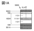
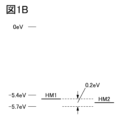
- FIGS. 1A and 1B are diagrams illustrating the configuration of a light emitting device according to an embodiment.
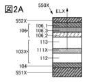
- 2A and 2B are diagrams illustrating the configuration of a light emitting device according to an embodiment.
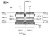
- 3A and 3B are diagrams illustrating the configuration of a display device according to an embodiment.
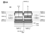
- FIGS. 4A and 4B are diagrams illustrating the configuration of a display device according to an embodiment.
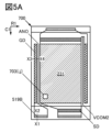
- 5A to 5C are diagrams illustrating the configuration of an apparatus according to an embodiment.
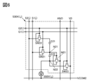
- FIG. 6 is a diagram illustrating the configuration of the device according to the embodiment.
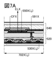
- 7A and 7B are diagrams illustrating the configuration of an apparatus according to an embodiment.
- FIGS. 8A and 8B are diagrams illustrating the configuration of an active matrix light emitting device according to an embodiment.
- FIGS. 9A and 9B are diagrams illustrating the configuration of an active matrix light emitting device according to an embodiment.
- FIG. 10 is a diagram illustrating the configuration of an active matrix light emitting device according to an embodiment.
- FIGS. 11A and 11B are diagrams illustrating the configuration of a passive matrix light emitting device according to an embodiment.
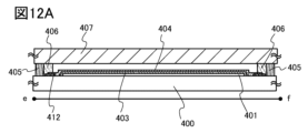
- 12A and 12B are diagrams illustrating the configuration of a lighting device according to an embodiment.
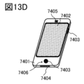
- 13A to 13D are diagrams illustrating the configuration of an electronic device according to an embodiment.
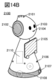
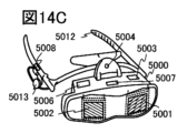
- 14A to 14C are diagrams illustrating the configuration of an electronic device according to an embodiment.
- FIG. 15 is a diagram illustrating the configuration of the lighting device according to the embodiment.
- FIG. 16 is a diagram illustrating the configuration of the lighting device according to the embodiment.
- FIG. 17 is a diagram illustrating the configuration of an in-vehicle display device and a lighting device according to an embodiment.
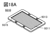
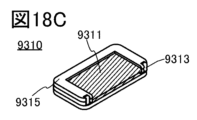
- 18A to 18C are diagrams illustrating the configuration of an electronic device according to an embodiment.
- FIG. 19 is a diagram illustrating a proton NMR spectrum of an organic compound according to an example.
- FIG. 20 is a diagram illustrating absorption spectra and emission spectra of organic compounds according to Examples.
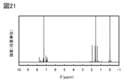
- FIG. 21 is a diagram illustrating a proton NMR spectrum of an organic compound according to an example.
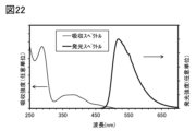
- FIG. 22 is a diagram illustrating absorption spectra and emission spectra of organic compounds according to Examples.
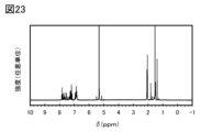
- FIG. 23 is a diagram illustrating a proton NMR spectrum of an organic compound according to an example.
- FIG. 24 is a diagram illustrating absorption spectra and emission spectra of organic compounds according to Examples.
- FIG. 25 is a diagram illustrating a proton NMR spectrum of an organic compound according to an example.
- FIG. 26 is a diagram illustrating absorption spectra and emission spectra of organic compounds according to Examples.
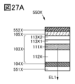
- FIG. 27 is a diagram illustrating the configuration of a light emitting device according to an example.
- FIG. 28 is a diagram illustrating current density-luminance characteristics of the light emitting device according to the example.
- FIG. 29 is a diagram illustrating the luminance-current efficiency characteristics of the light emitting device according to the example.
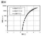
- FIG. 30 is a diagram illustrating voltage-luminance characteristics of the light emitting device according to the example.
- FIG. 31 is a diagram illustrating voltage-current characteristics of the light emitting device according to the example.
- FIG. 32 is a diagram illustrating the luminance-external quantum efficiency characteristics of the light emitting device according to the example.
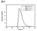
- FIG. 33 is a diagram illustrating the emission spectrum of the light emitting device according to the example.
- FIG. 34 is a diagram illustrating the change over time in the normalized luminance of the light emitting device according to the example.
- the organic compound of one embodiment of the present invention is represented by general formula (G0).
- X is a nitrogen atom or a carbon atom, and when X is a carbon atom, X is bonded to hydrogen or a substituent.
- one of R 104 and R 105 is a cyano group, at least one of R 102 and R 107 is an alkyl group having 1 to 6 carbon atoms, and each of R 101 to R 111 is independently , hydrogen or a substituent.
- substituents each independently represent an alkyl group having 1 to 6 carbon atoms, a cycloalkyl group having 3 to 7 carbon atoms, a substituted or unsubstituted aryl group having 6 to 13 carbon atoms, or a substituted or unsubstituted aryl group having 6 to 13 carbon atoms. They are 1 to 5 heteroaryl groups, amino groups, or hydroxy groups, and may also be bonded to each other to form a ring. n is an integer of 1 or more and 3 or less, and L is a ligand.
- R 102 or R 107 brings about a steric hindrance effect between the phenyl group into which the cyano group has been introduced and the phenylpyridine skeleton to which iridium is coordinated.
- it suppresses the free rotation of the phenyl group into which the cyano group has been introduced, and improves the thermal properties of the compound, such as suppressing thermal decomposition. can be improved.
- the sublimability of sublimation without thermal decomposition can be improved.
- it can exhibit resistance to use in high-temperature environments.
- twisting occurs between the phenyl group into which the cyano group is introduced and the phenylpyridine skeleton to which iridium is coordinated.
- the emission wavelength can be shortened.
- high luminous efficiency can be achieved.
- a novel organic compound with excellent convenience, usefulness, or reliability can be provided.
- X is a nitrogen atom or a carbon atom, and when X is a carbon atom, X is bonded to hydrogen or a substituent.
- one of R 104 and R 105 is a cyano group
- at least one of R 102 and R 107 is an alkyl group having 1 to 6 carbon atoms
- other than R 101 to R 111 are each independently hydrogen or a substituent.
- the hydrogen may be substituted with deuterium.
- examples of the above alkyl group having 1 to 6 carbon atoms include methyl group, ethyl group, propyl group, butyl group, isobutyl group, sec-butyl group, tert-butyl group, pentyl group, hexyl group, etc. can be mentioned.
- part or all of the hydrogen in the alkyl group having 1 to 6 carbon atoms may be substituted with deuterium.
- the substituents bonded to X and R 101 to R 111 are each independently an alkyl group having 1 to 6 carbon atoms, a cycloalkyl group having 3 to 7 carbon atoms, a substituted or unsubstituted A substituted aryl group having 6 to 13 carbon atoms, a substituted or unsubstituted heteroaryl group having 1 to 5 carbon atoms, an amino group, or a hydroxy group. Further, the above substituents may be bonded to each other to form a ring.
- examples of the alkyl group having 1 to 6 carbon atoms include methyl group, ethyl group, propyl group, butyl group, isobutyl group, sec-butyl group, tert-butyl group, pentyl group, hexyl group, etc. can.
- examples of the above-mentioned cycloalkyl group having 3 to 7 carbon atoms include a cyclopropyl group, a cyclobutyl group, a cyclopentyl group, a cyclohexyl group, a 1-methylcyclohexyl group, a 2,6-dimethylcyclohexyl group, a cycloheptyl group, and a cycloalkyl group.
- examples of the substituent include an alkyl group having 1 to 6 carbon atoms and a phenyl group.
- examples of the above-mentioned aryl group having 6 to 13 carbon atoms include phenyl group, o-tolyl group, m-tolyl group, p-tolyl group, mesityl group, o-biphenyl group, m-biphenyl group, p-tolyl group, Examples include biphenyl group, 1-naphthyl group, 2-naphthyl group, and fluorenyl group.
- examples of the substituent include an alkyl group having 1 to 6 carbon atoms and a phenyl group.
- heteroaryl group having 1 to 5 carbon atoms examples include a pyridinyl group, a pyrimidinyl group, a pyridazinyl group, a pyrazinyl group, and a triazinyl group.
- substituents include an alkyl group having 1 to 6 carbon atoms and a phenyl group.
- examples of the above amino group include a methylamino group, an ethylamino group, an isopropylamino group, an isobutylamino group, a phenylamino group, and a 2,6-dimethylphenylamino group.
- n is an integer of 1 or more and 3 or less
- L is a ligand represented by structural formula (L0).
- R 201 to R 208 are each independently hydrogen or an alkyl group having 1 to 6 carbon atoms.
- the hydrogen may be substituted with deuterium.
- examples of the above alkyl group having 1 to 6 carbon atoms include methyl group, ethyl group, propyl group, butyl group, isobutyl group, sec-butyl group, tert-butyl group, pentyl group, hexyl group, etc. can be mentioned.
- part or all of the hydrogen in the alkyl group having 1 to 6 carbon atoms may be substituted with deuterium.
- n is 1 or 2
- 2-phenylpyridine can be used as the ligand L.
- all hydrogens may be deuterium.
- an organic compound of one embodiment of the present invention is represented by general formula (G1).
- X is a nitrogen atom or a carbon atom, and when X is a carbon atom, X is bonded to hydrogen or a substituent.
- At least one of R 102 and R 107 is an alkyl group having 1 to 6 carbon atoms, and the others from R 101 to R 111 are each independently hydrogen or a substituent. Note that the substituents may be bonded to each other to form a ring.
- the substituents each independently include an alkyl group having 1 to 6 carbon atoms, a cycloalkyl group having 3 to 7 carbon atoms, a substituted or unsubstituted aryl group having 6 to 13 carbon atoms, and a substituted or unsubstituted aryl group having 1 to 13 carbon atoms. 5, a heteroaryl group, an amino group, or a hydroxy group.
- n is an integer of 1 or more and 3 or less
- L is a ligand represented by structural formula (L1).
- R 201 to R 208 are each independently hydrogen or an alkyl group having 1 to 6 carbon atoms.
- all hydrogens may be deuterium.
- R 102 or R 107 brings about a steric hindrance effect between the phenyl group into which the cyano group has been introduced and the phenylpyridine skeleton to which iridium is coordinated.
- the sublimability of sublimation without thermal decomposition can be improved. In addition, it can exhibit resistance to use in high-temperature environments.
- twisting occurs between the phenyl group into which the cyano group is introduced and the phenylpyridine skeleton to which iridium is coordinated. Furthermore, the emission wavelength can be shortened. Furthermore, high luminous efficiency can be achieved. As a result, a novel organic compound with excellent convenience, usefulness, or reliability can be provided.
- an organic compound of one embodiment of the present invention is represented by general formula (G2).
- R 102 and R 107 are each independently hydrogen or a substituent. Note that the substituents may be bonded to each other to form a ring.
- the substituents each independently include an alkyl group having 1 to 6 carbon atoms, a cycloalkyl group having 3 to 7 carbon atoms, a substituted or unsubstituted aryl group having 6 to 13 carbon atoms, and a substituted or unsubstituted aryl group having 1 to 13 carbon atoms. 5, a heteroaryl group, an amino group, or a hydroxy group.
- an organic compound of one embodiment of the present invention is represented by general formula (G3).
- R 102 and R 107 are each independently hydrogen or a substituent. Note that the substituents may be bonded to each other to form a ring.
- the substituents each independently include an alkyl group having 1 to 6 carbon atoms, a cycloalkyl group having 3 to 7 carbon atoms, a substituted or unsubstituted aryl group having 6 to 13 carbon atoms, and a substituted or unsubstituted aryl group having 1 to 13 carbon atoms. 5, a heteroaryl group, an amino group, or a hydroxy group.
- an organic compound of one embodiment of the present invention is represented by general formula (G4).
- R 102 and R 107 are each independently hydrogen or a substituent. Note that the substituents may be bonded to each other to form a ring.
- the substituents each independently include an alkyl group having 1 to 6 carbon atoms, a cycloalkyl group having 3 to 7 carbon atoms, a substituted or unsubstituted aryl group having 6 to 13 carbon atoms, and a substituted or unsubstituted aryl group having 1 to 13 carbon atoms. 5, a heteroaryl group, an amino group or a hydroxy group.
- all hydrogens may be deuterium.
- X is a nitrogen atom or a carbon atom, and when X is a carbon atom, X is bonded to hydrogen or a substituent.
- one of R 104 and R 105 is a cyano group
- at least one of R 102 and R 107 is an alkyl group having 1 to 6 carbon atoms
- each of R 101 to R 111 is independently , hydrogen or a substituent.
- substituents each independently represent an alkyl group having 1 to 6 carbon atoms, a cycloalkyl group having 3 to 7 carbon atoms, a substituted or unsubstituted aryl group having 6 to 13 carbon atoms, or a substituted or unsubstituted aryl group having 6 to 13 carbon atoms. They are 1 to 5 heteroaryl groups, amino groups, or hydroxy groups, and may also be bonded to each other to form a ring.
- n is an integer of 1 or more and 3 or less
- L is a ligand represented by structural formula (L0).
- R 201 to R 208 are each independently hydrogen or an alkyl group having 1 to 6 carbon atoms, and in the general formula (G0), all hydrogens are deuterium. It's okay.
- a pyridine derivative represented by the general formula (Gpy0) and a metal compound of iridium containing a halogen iridium chloride hydrate, ammonium hexachloroiridate, etc.
- an organic compound represented by general formula (G0) can be synthesized by mixing with a metal complex compound (acetylacetonate complex, diethyl sulfide complex, etc.) and then heating.
- a pyridine derivative represented by the general formula (Gpy0) and a halogen-containing iridium metal compound or an iridium organometallic complex compound are mixed in an alcoholic solvent (glycerol, ethylene glycol, 2-methoxyethanol, 2-ethoxyethanol).
- the organic compound represented by the general formula (G0) can also be synthesized by dissolving the compound in a compound (e.g.) and heating it.
- X is a nitrogen atom or a carbon atom, and when X is a carbon atom, X is bonded to hydrogen or a substituent.
- one of R 104 and R 105 is a cyano group
- at least one of R 102 and R 107 is an alkyl group having 1 to 6 carbon atoms
- each of R 101 to R 111 is independently , hydrogen or a substituent.
- substituents each independently represent an alkyl group having 1 to 6 carbon atoms, a cycloalkyl group having 3 to 7 carbon atoms, a substituted or unsubstituted aryl group having 6 to 13 carbon atoms, or a substituted or unsubstituted aryl group having 6 to 13 carbon atoms. They are 1 to 5 heteroaryl groups, amino groups, or hydroxy groups, and may also be bonded to each other to form a ring.
- n is an integer of 1 or more and 3 or less
- L is a ligand represented by structural formula (L0).
- R 201 to R 208 are each independently hydrogen or an alkyl group having 1 to 6 carbon atoms, and in the general formula (G0), each hydrogen may be deuterium. good.
- the organometallic complex that is one embodiment of the present invention is characterized by having a wide variety of ligands.
- FIG. 1A is a cross-sectional view illustrating the structure of a light-emitting device according to one embodiment of the present invention
- FIG. 1B is a diagram illustrating energy levels of materials used in the light-emitting device according to one embodiment of the present invention.
- a light emitting device 550X described in this embodiment includes an electrode 551X, an electrode 552X, and a unit 103X. Electrode 552X overlaps electrode 551X, and unit 103X is sandwiched between electrode 552X and electrode 551X.
- the unit 103X has a single layer structure or a laminated structure.
- unit 103X includes layer 111X, layer 112, and layer 113 (see FIG. 1A).
- the unit 103X has a function of emitting light ELX.
- Layer 111X is sandwiched between layer 113 and layer 112
- layer 113 is sandwiched between electrode 552X and layer 111X
- layer 112 is sandwiched between layer 111X and electrode 551X.
- a layer selected from layers having functions such as a light emitting layer, a hole transport layer, an electron transport layer, and a carrier block layer can be used for the unit 103X.
- a layer selected from functional layers such as a hole injection layer, an electron injection layer, an exciton blocking layer, and a charge generation layer can be used for the unit 103X.
- layer 112 a material with hole transporting properties can be used for layer 112. Further, layer 112 can be referred to as a hole transport layer. Note that a structure in which a material having a larger band gap than the light-emitting material included in the layer 111X is used for the layer 112 is preferable. Thereby, energy transfer from excitons to the layer 112 that occurs in the layer 111X can be suppressed.
- a material having a hole mobility of 1 ⁇ 10 ⁇ 6 cm 2 /Vs or more can be suitably used as a material having hole transport properties.
- an amine compound or an organic compound having a ⁇ -electron-excessive heteroaromatic ring skeleton can be used as the material having hole transport properties.
- a compound having an aromatic amine skeleton, a compound having a carbazole skeleton, a compound having a thiophene skeleton, a compound having a furan skeleton, etc. can be used.
- a compound having an aromatic amine skeleton or a compound having a carbazole skeleton is preferable because it has good reliability, high hole transportability, and contributes to reducing the driving voltage.
- Examples of compounds having an aromatic amine skeleton include 4,4'-bis[N-(1-naphthyl)-N-phenylamino]biphenyl (abbreviation: NPB), N,N'-diphenyl-N,N' -bis(3-methylphenyl)-4,4'-diaminobiphenyl (abbreviation: TPD), 4,4'-bis(9,9'-spirobi[9H-fluoren]-2-yl)-N,N' -diphenyl-4,4'-diaminobiphenyl (abbreviation: BSPB), 4-phenyl-4'-(9-phenylfluoren-9-yl)triphenylamine (abbreviation: BPAFLP), 4-phenyl-3'-( 9-phenylfluoren-9-yl)triphenylamine (abbreviation: mBPAFLP), 4-phenyl-4'-(9-phenyl-9H-c
- Examples of compounds having a carbazole skeleton include 1,3-bis(N-carbazolyl)benzene (abbreviation: mCP), 4,4'-di(N-carbazolyl)biphenyl (abbreviation: CBP), 3,6-bis (3,5-diphenylphenyl)-9-phenylcarbazole (abbreviation: CzTP), 9,9'-diphenyl-9H,9'H-3,3'-bicarbazole (abbreviation: PCCP), etc. can be used. can.
- mCP 1,3-bis(N-carbazolyl)benzene
- CBP 4,4'-di(N-carbazolyl)biphenyl
- CzTP 3,6-bis (3,5-diphenylphenyl)-9-phenylcarbazole
- PCCP 9,9'-diphenyl-9H,9'H-3,3'-bicarbazole
- Examples of compounds having a thiophene skeleton include 4,4',4''-(benzene-1,3,5-triyl)tri(dibenzothiophene) (abbreviation: DBT3P-II), 2,8-diphenyl-4 -[4-(9-phenyl-9H-fluoren-9-yl)phenyl]dibenzothiophene (abbreviation: DBTFLP-III), 4-[4-(9-phenyl-9H-fluoren-9-yl)phenyl]- 6-phenyldibenzothiophene (abbreviation: DBTFLP-IV), etc. can be used.
- DBT3P-II 4,4',4''-(benzene-1,3,5-triyl)tri(dibenzothiophene)
- DBTFLP-III 2,8-diphenyl-4 -[4-(9-phenyl-9H-fluoren-9-yl)pheny
- Examples of compounds having a furan skeleton include 4,4',4''-(benzene-1,3,5-triyl)tri(dibenzofuran) (abbreviation: DBF3P-II), 4- ⁇ 3-[3- (9-phenyl-9H-fluoren-9-yl)phenyl]phenyl ⁇ dibenzofuran (abbreviation: mmDBFFLBi-II), etc. can be used.
- DBF3P-II 4,4',4''-(benzene-1,3,5-triyl)tri(dibenzofuran)
- mmDBFFLBi-II 4- ⁇ 3-[3- (9-phenyl-9H-fluoren-9-yl)phenyl]phenyl ⁇ dibenzofuran
- ⁇ Configuration example of layer 113>> For example, a material having an electron transport property, a material having an anthracene skeleton, a mixed material, or the like can be used for the layer 113. Furthermore, the layer 113 can be referred to as an electron transport layer. Note that a structure in which a material having a larger band gap than the light-emitting material included in the layer 111X is used for the layer 113 is preferable. Thereby, energy transfer from excitons generated in the layer 111X to the layer 113 can be suppressed.
- a metal complex or an organic compound having a ⁇ -electron-deficient heteroaromatic ring skeleton can be used as the material having electron transport properties.
- metal complexes include bis(10-hydroxybenzo[h]quinolinato) beryllium(II) (abbreviation: BeBq 2 ), bis(2-methyl-8-quinolinolato)(4-phenylphenolato)aluminum(III) (abbreviation: BAlq), bis(8-quinolinolato)zinc(II) (abbreviation: Znq), bis[2-(2-benzooxazolyl)phenolato]zinc(II) (abbreviation: ZnPBO), bis[2- (2-benzothiazolyl)phenolato]zinc(II) (abbreviation: ZnBTZ), etc. can be used.
- Examples of the organic compound having a ⁇ electron-deficient heteroaromatic ring skeleton include a heterocyclic compound having a polyazole skeleton, a heterocyclic compound having a diazine skeleton, a heterocyclic compound having a pyridine skeleton, a heterocyclic compound having a triazine skeleton, etc. Can be used.
- a heterocyclic compound having a diazine skeleton or a heterocyclic compound having a pyridine skeleton is preferable because of its good reliability.
- a heterocyclic compound having a diazine (pyrimidine or pyrazine) skeleton has high electron transport properties and can reduce the driving voltage.
- heterocyclic compound having a polyazole skeleton examples include 2-(4-biphenylyl)-5-(4-tert-butylphenyl)-1,3,4-oxadiazole (abbreviation: PBD), 3-(4 -biphenylyl)-4-phenyl-5-(4-tert-butylphenyl)-1,2,4-triazole (abbreviation: TAZ), 1,3-bis[5-(p-tert-butylphenyl)-1 , 3,4-oxadiazol-2-yl]benzene (abbreviation: OXD-7), 9-[4-(5-phenyl-1,3,4-oxadiazol-2-yl)phenyl]-9H -Carbazole (abbreviation: CO11), 2,2',2''-(1,3,5-benzentriyl)tris(1-phenyl-1H-benzimidazole) (abbreviation: TPBI), 2-[3-
- heterocyclic compound having a diazine skeleton examples include 2-[3-(dibenzothiophen-4-yl)phenyl]dibenzo[f,h]quinoxaline (abbreviation: 2mDBTPDBq-II), 2-[3'-(dibenzothiophen-4-yl)phenyl] Thiophen-4-yl)biphenyl-3-yl]dibenzo[f,h]quinoxaline (abbreviation: 2mDBTBPDBq-II), 2-[3'-(9H-carbazol-9-yl)biphenyl-3-yl]dibenzo[ f, h] Quinoxaline (abbreviation: 2mCzBPDBq), 4,6-bis[3-(phenanthren-9-yl)phenyl]pyrimidine (abbreviation: 4,6mPnP2Pm), 4,6-bis[3-(4-dibenzothienyl) )
- heterocyclic compound having a pyridine skeleton examples include 3,5-bis[3-(9H-carbazol-9-yl)phenyl]pyridine (abbreviation: 35DCzPPy), 1,3,5-tri[3-(3 -pyridyl)phenyl]benzene (abbreviation: TmPyPB), etc. can be used.
- heterocyclic compound having a triazine skeleton examples include 2-[3'-(9,9-dimethyl-9H-fluoren-2-yl)biphenyl-3-yl]-4,6-diphenyl-1,3, 5-triazine (abbreviation: mFBPTzn), 2-[(1,1'-biphenyl)-4-yl]-4-phenyl-6-[9,9'-spirobi(9H-fluorene)-2-yl]- 1,3,5-triazine (abbreviation: BP-SFTzn), 2- ⁇ 3-[3-(benzo[b]naphtho[1,2-d]furan-8-yl)phenyl]phenyl ⁇ -4,6 -diphenyl-1,3,5-triazine (abbreviation: mBnfBPTzn), 2- ⁇ 3-[3-(benzo[b]naphtho[1,2-d]furan-6-yl
- An organic compound having an anthracene skeleton can be used for layer 113.
- organic compounds containing both an anthracene skeleton and a heterocyclic skeleton can be suitably used.
- an organic compound containing both an anthracene skeleton and a nitrogen-containing five-membered ring skeleton can be used for the layer 113.
- an organic compound containing both a nitrogen-containing five-membered ring skeleton containing two heteroatoms in the ring and an anthracene skeleton can be used for the layer 113.
- a pyrazole ring, imidazole ring, oxazole ring, thiazole ring, etc. can be suitably used for the heterocyclic skeleton.
- an organic compound containing both an anthracene skeleton and a nitrogen-containing six-membered ring skeleton can be used for the layer 113.
- an organic compound containing both a nitrogen-containing six-membered ring skeleton containing two heteroatoms in the ring and an anthracene skeleton can be used for the layer 113.
- a pyrazine ring, a pyrimidine ring, a pyridazine ring, etc. can be suitably used for the heterocyclic skeleton.
- composition of mixed material a material that is a mixture of multiple types of substances can be used for the layer 113.
- a mixed material containing an alkali metal, an alkali metal compound, or an alkali metal complex, and a substance having electron transport properties can be used for the layer 113.
- the highest occupied molecular orbital (HOMO) level of the material having electron transporting properties is ⁇ 6.0 eV or higher.
- a configuration in which the alkali metal, alkali metal compound, or alkali metal complex exists with a concentration difference (including the case of 0) in the thickness direction of the layer 113 is preferable.
- a metal complex containing an 8-hydroxyquinolinato structure can be used.
- a methyl substituted product for example, a 2-methyl substituted product or a 5-methyl substituted product
- a metal complex containing an 8-hydroxyquinolinato structure can also be used.
- 8-hydroxyquinolinato-lithium abbreviation: Liq
- 8-hydroxyquinolinato-sodium abbreviation: Naq
- monovalent metal ion complexes especially lithium complexes, are preferred, and Liq is more preferred.
- the mixed material can be suitably used for layer 113.
- a composite material of a substance having electron-accepting properties and a material having hole-transporting properties can be used for the layer 104.
- a composite material of a substance having electron-accepting properties and a substance having a relatively deep HOMO level HM1 of ⁇ 5.7 eV or more and ⁇ 5.4 eV or less can be used for the layer 104 (FIG. 1B reference).
- the configuration in which the mixed material is used for the layer 113 and the composite material is used in the layer 104 is preferable to combine with the configuration in which a material having hole transport properties is used in the layer 112.
- a material having a HOMO level HM2 in the range of ⁇ 0.2 eV or more and 0 eV or less compared to the relatively deep HOMO level HM1 can be used for the layer 112 (see FIG. 1B).
- the reliability of the light emitting device can be improved.
- the above light emitting device may be referred to as a Recombination-Site Tailoring Injection structure (ReSTI structure).
- ⁇ Configuration example 1 of layer 111X>> For example, a luminescent material or a luminescent material and a host material can be used in layer 111X. Further, the layer 111X can be called a light emitting layer. Note that a configuration in which the layer 111X is arranged in a region where holes and electrons recombine is preferable. Thereby, energy generated by carrier recombination can be efficiently converted into light and emitted.
- the layer 111X is placed away from the metal used for the electrodes and the like. This makes it possible to suppress the quenching phenomenon caused by the metal used for the electrodes and the like.
- the distance from the reflective electrode or the like to the layer 111X is adjusted and the layer 111X is arranged at an appropriate position according to the emission wavelength.
- the light spectrum can be narrowed by intensifying the light of a predetermined wavelength.
- bright luminescent colors and strong intensity can be obtained.
- a microresonator structure microcavity
- a microresonator structure can be configured by arranging the layer 111X at an appropriate position between electrodes and the like.
- the luminescent material for example, a phosphorescent substance can be used. Thereby, the energy generated by carrier recombination can be emitted from the luminescent material as light ELX (see FIG. 1A).
- a phosphorescent material can be used in layer 111X.
- the organic compound of one embodiment of the present invention described in Embodiment 1 can be used for the layer 111X.
- Layer 111X contains the organic compound of one embodiment of the present invention. This suppresses the free rotation of the phenyl group into which the cyano group has been introduced, making it possible to improve the thermal properties of the compound, for example, to suppress thermal decomposition. Moreover, the sublimability of sublimation without thermal decomposition can be improved. In addition, it can exhibit resistance to use in high-temperature environments. Furthermore, the emission wavelength can be shortened due to the twist that occurs between the phenyl group into which the cyano group is introduced and the phenylpyridine skeleton to which iridium is coordinated. Furthermore, high luminous efficiency can be achieved. As a result, a novel light emitting device with excellent convenience, usefulness, and reliability can be provided.
- a material having carrier transport properties can be used as the host material.
- materials that have hole transport properties, materials that have electron transport properties, substances that exhibit thermally activated delayed fluorescence (TADF), materials that have an anthracene skeleton, and mixed materials of two or more selected from these. can be used as the host material.
- TADF thermally activated delayed fluorescence
- materials that have an anthracene skeleton, and mixed materials of two or more selected from these. can be used as the host material.
- TADF thermally activated delayed fluorescence
- a configuration in which a material having a larger band gap than the luminescent material included in the layer 111X is used as the host material is preferable. Thereby, energy transfer from excitons to the host material occurring in the layer 111X can be suppressed.
- a material having a hole mobility of 1 ⁇ 10 ⁇ 6 cm 2 /Vs or more can be suitably used as a material having hole transport properties.
- a material having hole transport properties that can be used for the layer 112 can be used as the host material.
- a metal complex or an organic compound having a ⁇ -electron-deficient heteroaromatic ring skeleton can be used as a material having electron transport properties.
- a material having electron transporting properties that can be used for the layer 113 can be used as the host material.
- a material that is a mixture of multiple types of substances can be used as the host material.
- a material having an electron transporting property and a material having a hole transporting property can be used as a mixed material.
- the organic compound of one embodiment of the present invention can be used as a host material.
- the organic compound of one embodiment of the present invention is a phosphorescent substance, and the phosphorescent substance can be used as an energy donor that provides excitation energy to the fluorescent substance when the fluorescent substance is used as the luminescent substance.
- the emission spectrum of the organic compound of one embodiment of the present invention includes light with a wavelength shorter than 500 nm, a fluorescent light-emitting material with an absorption spectrum that overlaps with the emission spectrum, for example, a green emission color.
- a fluorescent light-emitting material with an absorption spectrum that overlaps with the emission spectrum, for example, a green emission color.
- energy can be efficiently transferred to the fluorescent light-emitting material.
- the reliability of the light emitting device can be improved. As a result, a novel light emitting device with excellent convenience, usefulness, and reliability can be provided.
- a mixed material containing a material that forms an exciplex can be used for the host material.
- a material in which the emission spectrum of the exciplex formed overlaps with the wavelength of the lowest energy absorption band of the luminescent substance can be used as the host material.
- a mixed material containing a material having an electron transporting property and a material having a hole transporting property can be used as the material forming the exciplex.
- the driving voltage can be suppressed.
- a phosphorescent substance can also be used as at least one of the materials forming the exciplex. This makes it possible to utilize inverse intersystem crossing. Further, triplet excitation energy can be efficiently converted to singlet excitation energy.
- the HOMO level of the material having hole transporting properties is higher than the HOMO level of the material having electron transporting properties.
- the lowest unoccupied molecular orbital (LUMO) level of the material having hole transporting properties is equal to or higher than the LUMO level of the material having electron transporting properties.
- the formation of an exciplex is determined by comparing, for example, the emission spectrum of a material with hole-transporting properties, the emission spectrum of a material with electron-transporting properties, and the emission spectrum of a mixed film made by mixing these materials. This can be confirmed by observing the phenomenon that the emission spectrum of each material shifts to longer wavelengths (or has a new peak on the longer wavelength side).
- the transient PL life of the mixed film is calculated as follows: This can be confirmed by observing differences in transient response, such as having a longer-life component than the transient PL life of each material, or having a larger proportion of delayed components.
- the above-mentioned transient PL may be read as transient electroluminescence (EL).
- a light emitting device 550X described in this embodiment includes an electrode 551X, an electrode 552X, a unit 103X, and a layer 104. Electrode 552X overlaps electrode 551X, and unit 103X is sandwiched between electrode 551X and electrode 552X. Further, layer 104 is sandwiched between electrode 551X and unit 103X. Note that, for example, the configuration described in Embodiment 2 can be used for the unit 103X.
- a conductive material can be used for electrode 551X.
- a film containing a metal, an alloy, or a conductive compound can be used for the electrode 551X in a single layer or a stacked layer.
- a film that efficiently reflects light can be used for the electrode 551X.
- an alloy containing silver and copper, an alloy containing silver and palladium, or a metal film such as aluminum can be used for the electrode 551X.
- a metal film that transmits part of the light and reflects the other part of the light can be used for the electrode 551X.
- a microresonator structure microwave cavity
- light of a predetermined wavelength can be extracted more efficiently than other light.
- light with a narrow half-value width of the spectrum can be extracted. Or you can extract brightly colored light.
- a film that transmits visible light can be used for the electrode 551X.
- a metal film, an alloy film, a conductive oxide film, or the like that is thin enough to transmit light can be used for the electrode 551X in a single layer or a stacked layer.
- a material having a work function of 4.0 eV or more can be suitably used for the electrode 551X.
- a conductive oxide containing indium can be used. Specifically, it contains indium oxide, indium oxide-tin oxide (abbreviation: ITO), indium oxide-tin oxide containing silicon or silicon oxide (abbreviation: ITSO), indium oxide-zinc oxide, tungsten oxide, and zinc oxide. Indium oxide (abbreviation: IWZO) or the like can be used.
- a conductive oxide containing zinc can be used.
- zinc oxide, zinc oxide added with gallium, zinc oxide added with aluminum, etc. can be used.
- gold Au
- platinum Pt
- nickel Ni
- tungsten W
- Cr chromium
- Mo molybdenum
- iron Fe
- Co cobalt
- Cu copper
- palladium Pd
- a nitride of a metal material for example, titanium nitride
- graphene can be used.
- ⁇ Configuration example 1 of layer 104>> a material with hole injection properties can be used for layer 104.
- the layer 104 can be referred to as a hole injection layer.
- the layer 104 For example, a material whose hole mobility is 1 ⁇ 10 ⁇ 3 cm/Vs or less when the square root of the electric field strength V/cm is 600 can be used for the layer 104 . Further, a film having an electrical resistivity of 1 ⁇ 10 4 ⁇ cm or more and 1 ⁇ 10 7 ⁇ cm or less can be used for the layer 104. Preferably, the layer 104 has an electrical resistivity of 5 ⁇ 10 4 ⁇ cm to 1 ⁇ 10 7 ⁇ cm, more preferably 1 ⁇ 10 5 ⁇ cm to 1 ⁇ 10 7 ⁇ cm. It has an electrical resistivity of cm or less.
- Organic and inorganic compounds can be used as materials with electron-accepting properties.
- a substance having electron-accepting properties can extract electrons from an adjacent hole-transporting layer or a material having hole-transporting properties by applying an electric field.
- a compound having an electron-withdrawing group (halogen group or cyano group) can be used as a substance having electron-accepting properties.
- an organic compound having electron-accepting properties is easily vapor-deposited and can be easily formed into a film. Thereby, the productivity of the light emitting device 550X can be increased.
- a compound such as HAT-CN in which an electron-withdrawing group is bonded to a condensed aromatic ring having a plurality of heteroatoms is thermally stable and is therefore preferable.
- [3]radialene derivatives having an electron-withdrawing group are preferable because they have very high electron-accepting properties.
- ⁇ , ⁇ ', ⁇ ''-1,2,3-cyclopropane triylidenetris [4-cyano-2,3,5,6-tetrafluorobenzeneacetonitrile]
- ⁇ , ⁇ ', ⁇ ''-1,2,3-cyclopropane triylidene tris [2,6-dichloro-3,5-difluoro-4-(trifluoromethyl)benzeneacetonitrile]
- ⁇ , ⁇ ', ⁇ ''-1,2 , 3-cyclopropane triylidene tris [2,3,4,5,6-pentafluorobenzeneacetonitrile], etc.
- transition metal oxides such as molybdenum oxide, vanadium oxide, ruthenium oxide, tungsten oxide, and manganese oxide can be used as the substance having electron-accepting properties.
- phthalocyanine compounds or complex compounds such as phthalocyanine (abbreviation: H2Pc) and copper phthalocyanine (abbreviation: CuPc), 4,4'-bis[N-(4-diphenylaminophenyl)-N-phenylamino]biphenyl (
- Aromatic amine skeletons such as N,N'-bis[4-bis(3-methylphenyl)aminophenyl]-N,N'-diphenyl-4,4'-diaminobiphenyl (abbreviation: DNTPD)
- DNTPD diaminobiphenyl
- polymers such as poly(3,4-ethylenedioxythiophene)/poly(styrene sulfonic acid) (PEDOT/PSS) can be used.
- a composite material including a substance having an electron-accepting property and a material having a hole-transporting property can be used for the layer 104.
- a material with a large work function but also a material with a small work function can be used for the electrode 551X.
- the material used for the electrode 551X can be selected from a wide range of materials regardless of the work function.
- compounds with aromatic amine skeletons, carbazole derivatives, aromatic hydrocarbons, aromatic hydrocarbons with vinyl groups, and polymer compounds (oligomers, dendrimers, polymers, etc.) are used to transport holes in composite materials. It can be used for materials with properties. Further, a material having a hole mobility of 1 ⁇ 10 ⁇ 6 cm 2 /Vs or more can be suitably used as a material having hole transport properties of a composite material. For example, a material with hole transporting properties that can be used for layer 112 can be used in the composite material.
- a substance having a relatively deep HOMO level can be suitably used as a material having hole transporting properties in a composite material.
- the HOMO level is preferably ⁇ 5.7 eV or more and ⁇ 5.4 eV or less.
- Examples of compounds having an aromatic amine skeleton include N,N'-di(p-tolyl)-N,N'-diphenyl-p-phenylenediamine (abbreviation: DTDPPA), 4,4'-bis[N- (4-diphenylaminophenyl)-N-phenylamino]biphenyl (abbreviation: DPAB), N,N'-bis[4-bis(3-methylphenyl)aminophenyl]-N,N'-diphenyl-4,4 '-diaminobiphenyl (abbreviation: DNTPD), 1,3,5-tris[N-(4-diphenylaminophenyl)-N-phenylamino]benzene (abbreviation: DPA3B), etc. can be used.
- DTDPPA 4,4'-bis[N- (4-diphenylaminophenyl)-N-phenylamino]biphenyl
- carbazole derivatives include 3-[N-(9-phenylcarbazol-3-yl)-N-phenylamino]-9-phenylcarbazole (abbreviation: PCzPCA1), 3,6-bis[N-(9- phenylcarbazol-3-yl)-N-phenylamino]-9-phenylcarbazole (abbreviation: PCzPCA2), 3-[N-(1-naphthyl)-N-(9-phenylcarbazol-3-yl)amino]- 9-phenylcarbazole (abbreviation: PCzPCN1), 4,4'-di(N-carbazolyl)biphenyl (abbreviation: CBP), 1,3,5-tris[4-(N-carbazolyl)phenyl]benzene (abbreviation: TCPB) ), 9-[4-(10-phenyl-9-anthracenyl)phenyl
- aromatic hydrocarbons examples include 2-tert-butyl-9,10-di(2-naphthyl)anthracene (abbreviation: t-BuDNA), 2-tert-butyl-9,10-di(1-naphthyl) Anthracene, 9,10-bis(3,5-diphenylphenyl)anthracene (abbreviation: DPPA), 2-tert-butyl-9,10-bis(4-phenylphenyl)anthracene (abbreviation: t-BuDBA), 9, 10-di(2-naphthyl)anthracene (abbreviation: DNA), 9,10-diphenylanthracene (abbreviation: DPAnth), 2-tert-butylanthracene (abbreviation: t-BuAnth), 9,10-bis(4-methyl -1-naphthyl)anthracene (abbreviation: DMNA
- aromatic hydrocarbons having a vinyl group examples include 4,4'-bis(2,2-diphenylvinyl)biphenyl (abbreviation: DPVBi), 9,10-bis[4-(2,2- diphenylvinyl)phenyl]anthracene (abbreviation: DPVPA), etc. can be used.
- DPVBi 4,4'-bis(2,2-diphenylvinyl)biphenyl
- DPVPA 9,10-bis[4-(2,2- diphenylvinyl)phenyl]anthracene
- polymer compounds include poly(N-vinylcarbazole) (abbreviation: PVK), poly(4-vinyltriphenylamine) (abbreviation: PVTPA), poly[N-(4- ⁇ N'-[4- (4-diphenylamino)phenyl]phenyl-N'-phenylamino ⁇ phenyl)methacrylamide] (abbreviation: PTPDMA), poly[N,N'-bis(4-butylphenyl)-N,N'-bis(phenyl) ) benzidine] (abbreviation: Poly-TPD), etc. can be used.
- PVK poly(N-vinylcarbazole)
- PVTPA poly(4-vinyltriphenylamine)
- PTPDMA poly[N-(4- ⁇ N'-[4- (4-diphenylamino)phenyl]phenyl-N'-phenylamino ⁇ phenyl)methacrylamide]
- a substance having any one of a carbazole skeleton, a dibenzofuran skeleton, a dibenzothiophene skeleton, and an anthracene skeleton can be suitably used as a material having a hole transporting property of a composite material.
- an aromatic amine having a substituent containing a dibenzofuran ring or a dibenzothiophene ring, an aromatic monoamine having a naphthalene ring, or a substance comprising an aromatic monoamine in which a 9-fluorenyl group is bonded to the nitrogen of the amine via an arylene group. it can be used for composite materials having hole transport properties. Note that by using a substance having an N,N-bis(4-biphenyl)amino group, the reliability of the light emitting device 550X can be improved.
- BnfABP N-(4-biphenyl)-6,N-diphenylbenzo[b]naphtho[1,2-d]furan-8-amine
- BnfABP N,N-bis( 4-biphenyl)-6-phenylbenzo[b]naphtho[1,2-d]furan-8-amine
- BBABnf 4,4'-bis(6-phenylbenzo[b]naphtho[1,2 -d]furan-8-yl)-4''-phenyltriphenylamine
- BnfBB1BP N,N-bis(4-biphenyl)benzo[b]naphtho[1,2-d]furan-6- Amine
- BBABnf (6) N,N-bis(4-biphenyl)benzo[b]naphtho[1,2-d]furan-8-amine
- a composite material containing a substance having electron-accepting properties, a material having hole-transporting properties, and an alkali metal fluoride or an alkaline earth metal fluoride may be used as a material having hole-injecting properties. I can do it.
- a composite material in which the atomic ratio of fluorine atoms is 20% or more can be suitably used. This allows the refractive index of the layer 104 to be lowered.
- a layer with a low refractive index can be formed inside the light emitting device 550X.
- the external quantum efficiency of the light emitting device 550X can be improved.
- a light emitting device 550X described in this embodiment includes an electrode 551X, an electrode 552X, a unit 103X, and a layer 105.
- the electrode 552X includes a region overlapping with the electrode 551X
- the unit 103X includes a region sandwiched between the electrode 551X and the electrode 552X.
- the layer 105 includes a region sandwiched between the unit 103X and the electrode 552X. Note that, for example, the configuration described in Embodiment 2 can be used for the unit 103X.
- a conductive material can be used for electrode 552X.
- a material containing a metal, an alloy, or a conductive compound can be used for the electrode 552X in a single layer or a laminated layer.
- the material that can be used for the electrode 551X described in Embodiment 3 can be used for the electrode 552X.
- a material having a smaller work function than the electrode 551X can be suitably used for the electrode 552X.
- a material having a work function of 3.8 eV or less is preferable.
- elements belonging to Group 1 of the Periodic Table of Elements elements belonging to Group 2 of the Periodic Table of Elements, rare earth metals, and alloys containing these can be used for the electrode 552X.
- An alloy of aluminum and silver or an alloy of aluminum and lithium can be used for electrode 552X.
- a material with electron injection properties can be used for layer 105.
- the layer 105 can be called an electron injection layer.
- a substance having electron donating properties can be used for the layer 105.
- a composite material of an electron-donating substance and an electron-transporting material can be used for the layer 105.
- electride can be used for layer 105.
- electrons can be easily injected from the electrode 552X.
- the material used for the electrode 552X can be selected from a wide range of materials regardless of the work function. Specifically, indium oxide-tin oxide containing Al, Ag, ITO, silicon, or silicon oxide can be used for the electrode 552X.
- the driving voltage of the light emitting device 550X can be reduced.
- Substance with electron donating property For example, alkali metals, alkaline earth metals, rare earth metals, or compounds thereof (oxides, halides, carbonates, etc.) can be used as the electron-donating substance.
- organic compounds such as tetrathianaphthacene (abbreviation: TTN), nickelocene, decamethylnickelocene, etc. can also be used as the electron-donating substance.
- Alkali metal compounds include lithium oxide, lithium fluoride (LiF), cesium fluoride (CsF), lithium carbonate, cesium carbonate, and 8-hydroxyquinolinate-lithium (abbreviation). :Liq), etc. can be used.
- Calcium fluoride (CaF 2 ), etc. can be used as the alkaline earth metal compound (including oxides, halides, and carbonates).
- a material that is a composite of multiple types of substances can be used as a material that has electron injection properties.
- a substance with electron-donating properties and a material with electron-transporting properties can be used in a composite material.
- a material with an electron mobility of 1 ⁇ 10 ⁇ 7 cm 2 /Vs or more and 5 ⁇ 10 ⁇ 5 cm 2 /Vs or less is It can be suitably used for materials that have Thereby, the amount of electrons injected into the light emitting layer can be controlled. Alternatively, it is possible to prevent the light-emitting layer from being in an electron-rich state.
- a metal complex or an organic compound having a ⁇ -electron-deficient heteroaromatic ring skeleton can be used as a material having electron transport properties.
- a material with electron transporting properties that can be used for layer 113 can be used for the composite material.
- a material having an electron transporting property with a microcrystalline alkali metal fluoride can be used in a composite material.
- a material having an electron transporting property with a microcrystalline alkaline earth metal fluoride can be used in the composite material.
- a composite material containing 50 wt % or more of an alkali metal fluoride or an alkaline earth metal fluoride can be suitably used.
- a composite material containing an organic compound having a bipyridine skeleton can be suitably used. This allows the refractive index of the layer 105 to be lowered. Alternatively, the external quantum efficiency of the light emitting device 550X can be improved.
- a composite material including a first organic compound with lone pairs of electrons and a first metal can be used for layer 105. Further, it is preferable that the total number of electrons of the first organic compound and the number of electrons of the first metal is an odd number.
- the molar ratio of the first metal to 1 mole of the first organic compound is preferably 0.1 or more and 10 or less, more preferably 0.2 or more and 2 or less, and even more preferably 0.2 or more and 0.8 or less. be.
- the first organic compound including the lone pair of electrons can interact with the first metal to form a single occupied molecular orbital (SOMO). Furthermore, when electrons are injected from the electrode 552X into the layer 105, a barrier between the two can be reduced.
- SOMO occupied molecular orbital
- the spin density measured using electron spin resonance (ESR) is preferably 1 ⁇ 10 16 spins/cm 3 or more, more preferably 5 ⁇ 10 16 spins/cm 3 or more, and even more preferably Composite materials that are 1 ⁇ 10 17 spins/cm 3 or higher can be used for layer 105.
- Organic compound with lone pair of electrons For example, a material having electron transporting properties can be used in an organic compound having a lone pair of electrons.
- a compound having an electron-deficient heteroaromatic ring can be used.
- a compound having at least one of a pyridine ring, a diazine ring (pyrimidine ring, pyrazine ring, pyridazine ring), and a triazine ring can be used. Thereby, the driving voltage of the light emitting device 550X can be reduced.
- the lowest unoccupied molecular orbital (LUMO) level of the organic compound having a lone pair of electrons is preferably ⁇ 3.6 eV or more and ⁇ 2.3 eV or less.
- the HOMO level and LUMO level of an organic compound can generally be estimated by CV (cyclic voltammetry), photoelectron spectroscopy, optical absorption spectroscopy, inverse photoelectron spectroscopy, or the like.
- BPhen 4,7-diphenyl-1,10-phenanthroline
- NBPhen 2,9-di(2-naphthyl)-4,7-diphenyl-1,10-phenanthroline
- HATNA diquinoxalino[2 ,3-a:2',3'-c]phenazine
- TmPPPyTz 2,4,6-tris[3'-(pyridin-3-yl)biphenyl-3-yl]-1,3,5 - Triazine
- TmPPPyTz 2,2'-(1,3-phenylene)bis(9-phenyl-1,10-phenanthroline)
- mPPhen2P 2,2'-(1,3-phenylene)bis(9-phenyl-1,10-phenanthroline
- mPPhen2P 2,2'-(1,3-phenylene)bis(9-phenyl-1,10-phenanthroline
- mPPhen2P 2,2'-(1,
- copper phthalocyanine can be used in organic compounds with lone pairs of electrons. Note that the number of electrons in copper phthalocyanine is an odd number.
- group metals aluminum (Al) and indium (In) are odd-numbered groups in the periodic table.
- the elements of Group 11 have a lower melting point than the elements of Group 7 or Group 9, and are suitable for vacuum evaporation.
- Ag is preferred because of its low melting point.
- the moisture resistance of the light emitting device 550X can be improved.
- a composite material of a first metal and a first organic compound that are in an even group in the periodic table may be used for the layer 105. I can do it.
- iron (Fe) a Group 8 metal, is an even group in the periodic table.
- Electrode For example, a material obtained by adding a high concentration of electrons to a mixed oxide of calcium and aluminum can be used as a material having electron injection properties.
- FIG. 2A is a cross-sectional view illustrating the structure of a light-emitting device according to one embodiment of the present invention.
- the light-emitting device 550X described in this embodiment includes an electrode 551X, an electrode 552X, a unit 103X, and a layer 106 (see FIG. 2A).
- the electrode 552X includes a region overlapping with the electrode 551X
- the unit 103X includes a region sandwiched between the electrode 551X and the electrode 552X.
- Layer 106 includes a region sandwiched between electrode 552X and unit 103X.
- the layer 106 has a function of supplying electrons to the anode side and supplying holes to the cathode side by applying a voltage. Further, the layer 106 can be referred to as a charge generation layer.
- a material having hole injection properties that can be used for layer 104 described in Embodiment 3 can be used for layer 106.
- composite materials can be used for layer 106.
- a laminated film in which a film containing the composite material and a film containing a material having hole transport properties are laminated can be used for the layer 106.
- the membrane containing the material having hole transport properties is sandwiched between the membrane containing the composite material and the cathode.
- Layer 106_1 includes a region sandwiched between unit 103X and electrode 552X
- layer 106_2 includes a region sandwiched between unit 103X and layer 106_1.
- ⁇ Configuration example of layer 106_1>> a material having hole injection properties that can be used for the layer 104 described in Embodiment 3 can be used for the layer 106_1.
- a composite material can be used for layer 106_1.
- a film having an electrical resistivity of 1 ⁇ 10 4 [ ⁇ cm] or more and 1 ⁇ 10 7 [ ⁇ cm] or less can be used for the layer 106_1.
- the layer 106_1 has an electrical resistivity of 5 ⁇ 10 4 [ ⁇ cm] or more and 1 ⁇ 10 7 [ ⁇ cm] or less, more preferably 1 ⁇ 10 5 [ ⁇ cm] or more. It has an electrical resistivity of 1 ⁇ 10 7 [ ⁇ cm] or less.
- ⁇ Configuration example of layer 106_2>> For example, the material that can be used for layer 105 described in Embodiment 4 can be used for layer 106_2.
- ⁇ Configuration example 3 of layer 106>> A stacked film in which the layer 106_1, the layer 106_2, and the layer 106_3 are stacked can be used for the layer 106.
- Layer 106_3 includes a region sandwiched between layer 106_1 and layer 106_2.
- a material having electron transport properties can be used for the layer 106_3.
- the layer 106_3 can be referred to as an electronic relay layer.
- the layer that is in contact with the anode side of the layer 106_3 can be moved away from the layer that is in contact with the cathode side of the layer 106_3.
- the interaction between the layer in contact with the anode side of the layer 106_3 and the layer in contact with the cathode side of the layer 106_3 can be reduced. Electrons can be smoothly supplied to the layer in contact with the anode side of the layer 106_3.
- a substance having a LUMO level is provided between the LUMO level of the substance having electron accepting properties contained in the layer in contact with the cathode side of the layer 106_3 and the LUMO level of the substance contained in the layer in contact with the anode side of the layer 106_3. , can be suitably used for the layer 106_3.
- a material having a LUMO level in the range of ⁇ 5.0 eV or more, preferably ⁇ 5.0 eV or more and ⁇ 3.0 eV or less can be used for the layer 106_3.
- a phthalocyanine-based material can be used for the layer 106_3.
- a phthalocyanine-based material can be used for the layer 106_3.
- copper phthalocyanine (abbreviation: CuPc) or a metal complex having a metal-oxygen bond and an aromatic ligand can be used for the layer 106_3.
- FIG. 2B is a cross-sectional view illustrating a structure of a light-emitting device according to one embodiment of the present invention, which has a structure different from that illustrated in FIG. 2A.
- a light emitting device 550X described in this embodiment includes an electrode 551X, an electrode 552X, a unit 103X, a layer 106, and a unit 103X2 (see FIG. 2B).
- Unit 103X is sandwiched between electrode 552X and electrode 551X, and layer 106 is sandwiched between electrode 552X and unit 103X.
- Unit 103X2 is sandwiched between electrode 552X and layer 106. Note that the unit 103X2 has a function of emitting the light ELX2.
- the light emitting device 550X has a plurality of stacked units between the electrode 551X and the electrode 552X.
- the number of units to be stacked is not limited to two, and three or more units can be stacked.
- a structure including a plurality of stacked units sandwiched between the electrode 551X and the electrode 552X and a layer 106 sandwiched between the plurality of units is referred to as a stacked-type light-emitting device or a tandem-type light-emitting device. There are cases where this happens.
- Unit 103X2 includes layer 111X2, layer 112_2, and layer 113_2. Layer 111X2 is sandwiched between layer 112_2 and layer 113_2.
- unit 103X The configuration that can be used for unit 103X can be used for unit 103X2.
- unit 103X2 the same configuration as unit 103X can be used for unit 103X2.
- a unit 103X that emits red light and green light and a unit 103X2 that emits blue light can be stacked and used. Thereby, it is possible to provide a light emitting device that emits light of a desired color. For example, a light emitting device that emits white light can be provided.
- the layer 106 has a function of supplying electrons to one of the unit 103X or the unit 103X2 and supplying holes to the other.
- the layer 106 described in Embodiment 5 can be used.
- each layer of the electrode 551X, the electrode 552X, the unit 103X, the layer 106, and the unit 103X2 can be formed using a dry method, a wet method, a vapor deposition method, a droplet discharge method, a coating method, a printing method, or the like. Also, different methods can be used to form each feature.
- the light emitting device 550X can be manufactured using a vacuum evaporation device, an inkjet device, a coating device such as a spin coater, a gravure printing device, an offset printing device, a screen printing device, or the like.
- the electrodes can be formed using a wet method or a sol-gel method using a paste of a metal material.
- an indium oxide-zinc oxide film can be formed by a sputtering method using a target in which 1 wt% or more and 20 wt% or less of zinc oxide is added to indium oxide.
- indium oxide containing tungsten oxide and zinc oxide (indium oxide) containing tungsten oxide and zinc oxide ( IWZO) film can be formed.
- FIG. 3A is a cross-sectional view illustrating a structure of a display device 700 according to one embodiment of the present invention
- FIG. 3B is a cross-sectional view illustrating a structure of a display device 700 according to one embodiment of the present invention, which is different from FIG. 3A. .
- a variable whose value is an integer of 1 or more may be used as a sign.
- (p) which includes a variable p that takes an integer value of 1 or more, may be used as part of a code that specifies any one of the maximum p components.
- (m, n) which includes a variable m and a variable n that take an integer value of 1 or more, may be used as a part of a code that specifies one of the maximum m ⁇ n components.
- the display device 700 described in this embodiment includes a light-emitting device 550X(i,j) and a light-emitting device 550Y(i,j) (see FIG. 3A).
- Light emitting device 550Y(i,j) is adjacent to light emitting device 550X(i,j).
- the display device 700 includes a substrate 510 and a functional layer 520.
- the functional layer 520 includes an insulating film 521, and the light emitting device 550X (i, j) and the light emitting device 550Y (i, j) are formed on the insulating film 521.
- Functional layer 520 is sandwiched between substrate 510, light emitting device 550X(i,j) and light emitting device 550Y(i,j).
- Light emitting device 550X(i, j) includes electrode 551X(i,j), electrode 552X(i,j), and unit 103X(i,j). Electrode 552X(i,j) overlaps electrode 551X(i,j), and unit 103X(i,j) is sandwiched between electrode 552X(i,j) and electrode 551X(i,j).
- the light emitting device 550X(i,j) has a layer 104X(i,j) and a layer 105X(i,j), and the layer 104X(i,j) has a unit 103X(i,j) and an electrode 551X(i , j), and layer 105X(i,j) is sandwiched between electrode 552X(i,j) and unit 103X(i,j).
- the unit 103X(i,j) includes a layer 111X(i,j), a layer 112X(i,j), and a layer 113X(i,j).
- the light-emitting device 550X described in Embodiments 2 to 6 can be used as the light-emitting device 550X(i,j).
- a configuration that can be used for electrode 551X can be used for electrode 551X (i, j)
- a configuration that can be used for electrode 552X can be used for electrode 552X (i, j).
- the configuration that can be used for the unit 103X can be used for the unit 103X(i,j).
- a structure that can be used for layer 104 can be used for layer 104X(i,j), and a structure that can be used for layer 105 can be used for layer 105X(i,j).
- a configuration that can be used for the layer 111X can be used for the layer 111X(i,j)
- a configuration that can be used for the layer 112 can be used for the layer 112X(i,j)
- a configuration that can be used for the layer 113 can be used for the layer 112X(i,j).
- a configuration that can be used for layer 113X(i,j) can be used.
- the light emitting device 550Y(i,j) includes an electrode 551Y(i,j), an electrode 552Y(i,j), and a unit 103Y(i,j). Electrode 552Y(i,j) overlaps electrode 551Y(i,j), and unit 103Y(i,j) is sandwiched between electrode 552Y(i,j) and electrode 551Y(i,j).
- the light emitting device 550Y(i,j) has a layer 104Y(i,j) and a layer 105Y(i,j), and the layer 104Y(i,j) has a unit 103Y(i,j) and an electrode 551Y(i , j), and layer 105Y(i,j) is sandwiched between electrode 552Y(i,j) and unit 103Y(i,j).
- Electrode 551Y(i,j) is adjacent to electrode 551X(i,j), and a gap 551XY(i,j) is provided between electrode 551Y(i,j) and electrode 551X(i,j).
- part of the configuration that can be used for the configuration of the light emitting device 550X (i, j) can be used for the configuration of the light emitting device 550Y (i, j).
- a part of the conductive film that can be used for the electrode 552X(i,j) can be used for the electrode 552Y(i,j).
- the structure that can be used for electrode 551X can be used for electrode 551Y(i,j).
- a structure that can be used for layer 104 can be used for layer 104Y(i,j), and a structure that can be used for layer 105 can be used for layer 105Y(i,j). This allows some of the configurations to be made common. Furthermore, the manufacturing process can be simplified.
- a configuration that emits light of the same hue as the emitted light color of the light emitting device 550X (i, j) can be used for the light emitting device 550Y (i, j).
- both light emitting device 550X(i,j) and light emitting device 550Y(i,j) may emit white light. Note that by placing a colored layer overlapping the light emitting device 550X (i, j), light of a predetermined hue can be extracted from white light. Further, another colored layer can be placed over the light emitting device 550Y(i,j) to extract light of another predetermined hue from the white light.
- both the light emitting device 550X(i,j) and the light emitting device 550Y(i,j) may emit blue light.
- a color conversion layer can be placed over the light emitting device 550X(i,j) to convert blue light into light of a predetermined hue.
- another color conversion layer can be placed over the light emitting device 550Y(i,j) to convert blue light to light of another predetermined hue. Blue light can be converted into green light or red light, for example.
- a configuration that emits light of a hue different from the emitted light color of the light emitting device 550X(i,j) can be used for the light emitting device 550Y(i,j).
- the hue of the light ELY emitted by the unit 103Y(i,j) can be made different from the hue of the light ELX.
- Light emitting device 550Y(i,j) differs from light emitting device 550X(i,j) in the configuration of layer 111Y(i,j).
- different parts will be described in detail, and the above description will be used for parts having the same configuration.
- ⁇ Configuration example of layer 111Y(i,j)>> For example, a luminescent material or a luminescent material and a host material can be used in layer 111Y(i,j). Further, the layer 111Y(i,j) can be called a light emitting layer. Note that a configuration in which the layer 111Y(i,j) is arranged in a region where holes and electrons recombine is preferable. Thereby, energy generated by carrier recombination can be efficiently converted into light and emitted.
- the layer 111Y(i,j) is placed away from the metal used for the electrodes and the like. This makes it possible to suppress the quenching phenomenon caused by the metal used for the electrodes and the like.
- the distance from the reflective electrode or the like to the layer 111Y(i,j) is adjusted and the layer 111Y(i,j) is arranged at an appropriate position according to the emission wavelength.
- the light spectrum can be narrowed by intensifying the light of a predetermined wavelength.
- bright luminescent colors and strong intensity can be obtained.
- a microresonator structure microcavity
- a microresonator structure can be configured by arranging the layer 111Y(i,j) at an appropriate position between electrodes and the like.
- a fluorescent material for example, a fluorescent material, a phosphorescent material, or a material exhibiting thermally activated delayed fluorescence (TADF) (also referred to as a TADF material) can be used as the luminescent material.
- TADF thermally activated delayed fluorescence
- Fluorescent materials can be used in layer 111Y(i,j).
- the fluorescent materials listed below can be used for the layer 111Y(i,j).
- the present invention is not limited thereto, and various known fluorescent light-emitting substances can be used for the layer 111Y(i,j).
- fused aromatic diamine compounds represented by pyrene diamine compounds such as 1,6FLPAPrn, 1,6mMemFLPAPrn, and 1,6BnfAPrn-03 are preferable because they have high hole-trapping properties and excellent luminous efficiency or reliability.
- N-[4-(9,10-diphenyl-2-anthryl)phenyl]-N,N',N'-triphenyl-1,4-phenylenediamine abbreviation: 2DPAPPA
- N,N,N' , N', N'', N'', N''', N'''-octaphenyldibenzo[g,p]chrysene-2,7,10,15-tetraamine abbreviation: DBC1
- DBC1 N-(9,10-diphenyl-2-anthryl)-N,9-diphenyl-9H-carbazol-3-amine
- 2PCAPA N-[9,10-bis(1,1'-biphenyl-2 -yl)-2-anthryl]-N,9-diphenyl-9H-carbazol-3-amine
- 2PCABPhA N-(9,10-diphenyl-2-
- DCM1 2-(2- ⁇ 2-[4-(dimethylamino)phenyl]ethenyl ⁇ -6-methyl-4H-pyran-4-ylidene)propanedinitrile
- DCM2 2- ⁇ 2-methyl- 6-[2-(2,3,6,7-tetrahydro-1H,5H-benzo[ij]quinolidin-9-yl)ethenyl]-4H-pyran-4-ylidene ⁇ propanedinitrile
- DCM2 N,N,N',N'-tetrakis(4-methylphenyl)tetracene-5,11-diamine
- p-mPhTD 7,14-diphenyl-N,N,N',N'-tetrakis( 4-methylphenyl)acenaphtho[1,2-a]fluoranthene-3,10-diamine
- p-mPhAFD 2- ⁇ 2-is
- a phosphorescent material can be used for layer 111Y(i,j).
- a phosphorescent material illustrated below can be used for the layer 111Y(i,j). Note that the present invention is not limited thereto, and various known phosphorescent materials can be used for the layer 111Y(i,j).
- organometallic iridium complexes having a 4H-triazole skeleton organometallic iridium complexes having a 1H-triazole skeleton, organometallic iridium complexes having an imidazole skeleton, organometallic iridium complexes having a phenylpyridine derivative having an electron-withdrawing group as a ligand.
- a complex, an organometallic iridium complex having a pyrimidine skeleton, an organometallic iridium complex having a pyrazine skeleton, an organometallic iridium complex having a pyridine skeleton, a rare earth metal complex, a platinum complex, etc. can be used for the layer 111Y(i,j). .
- organometallic iridium complexes having a 4H-triazole skeleton include tris ⁇ 2-[5-(2-methylphenyl)-4-(2,6-dimethylphenyl)-4H-1,2,4-triazole -3-yl- ⁇ N2]phenyl- ⁇ C ⁇ iridium(III) (abbreviation: [Ir(mpptz-dmp) 3 ]), tris(5-methyl-3,4-diphenyl-4H-1,2,4-triazolato) ) Iridium(III) (abbreviation: [Ir(Mptz) 3 ]), Tris[4-(3-biphenyl)-5-isopropyl-3-phenyl-4H-1,2,4-triazolato]iridium(III) ( Abbreviation: [Ir(iPrptz-3b) 3 ]), etc. can be used.
- organometallic iridium complexes having a 1H-triazole skeleton examples include tris[3-methyl-1-(2-methylphenyl)-5-phenyl-1H-1,2,4-triazolato]iridium(III) ( Abbreviation: [Ir(Mptz1-mp) 3 ]), tris(1-methyl-5-phenyl-3-propyl-1H-1,2,4-triazolato)iridium(III) (abbreviation: [Ir(Prptz1-Me) ) 3 ]), etc. can be used.
- organometallic iridium complexes having an imidazole skeleton examples include fac-tris[1-(2,6-diisopropylphenyl)-2-phenyl-1H-imidazole]iridium(III) (abbreviation: [Ir(iPrpim) 3 ]), tris[3-(2,6-dimethylphenyl)-7-methylimidazo[1,2-f]phenanthridinato]iridium(III) (abbreviation: [Ir(dmpimpt-Me) 3 ]), etc. can be used.
- organometallic iridium complexes having a phenylpyridine derivative having an electron-withdrawing group as a ligand include bis[2-(4',6'-difluorophenyl)pyridinato-N,C2 ' ]iridium(III).
- Tetrakis(1-pyrazolyl)borate (abbreviation: FIr6), bis[2-(4',6'-difluorophenyl)pyridinato-N,C2 ' ]iridium(III) picolinate (abbreviation: FIrpic), bis ⁇ 2- [3',5'-bis(trifluoromethyl)phenyl]pyridinato-N,C2 ' ⁇ iridium(III) picolinate (abbreviation: [Ir( CF3ppy ) 2 (pic)]), bis[2-( 4',6'-difluorophenyl)pyridinato-N, C2' ]iridium(III) acetylacetonate (abbreviation: FIracac), etc. can be used.
- FIrpic bis[2-(4',6'-difluorophenyl)pyridinato-N,C2 ' ]iridium(III)
- organometallic iridium complexes having a pyrimidine skeleton examples include tris(4-methyl-6-phenylpyrimidinato)iridium(III) (abbreviation: [Ir(mppm) 3 ]), tris(4-t-butyl -6-phenylpyrimidinato)iridium(III) (abbreviation: [Ir(tBuppm) 3 ]), (acetylacetonato)bis(6-methyl-4-phenylpyrimidinato)iridium(III) (abbreviation: [ Ir(mppm) 2 (acac)]), (acetylacetonato)bis(6-tert-butyl-4-phenylpyrimidinato)iridium(III) (abbreviation: [Ir(tBuppm) 2 (acac)]), (acetylacetonato)bis[6-(2-norbornyl
- organometallic iridium complexes having a pyrazine skeleton examples include (acetylacetonato)bis(3,5-dimethyl-2-phenylpyrazinato)iridium(III) (abbreviation: [Ir(mppr-Me) 2 ( acac)]), (acetylacetonato)bis(5-isopropyl-3-methyl-2-phenylpyrazinato)iridium(III) (abbreviation: [Ir(mppr-iPr) 2 (acac)]), etc. Can be used.
- organometallic iridium complexes having a pyridine skeleton examples include tris(2-phenylpyridinato-N,C 2' )iridium(III) (abbreviation: [Ir(ppy) 3 ]), bis(2-phenylpyridinato-N,C 2' )iridium(III) (abbreviation: [Ir(ppy) 3 ]), Pyridinato-N,C 2' )iridium(III) acetylacetonate (abbreviation: [Ir(ppy) 2 (acac)]), bis(benzo[h]quinolinato)iridium(III) acetylacetonate (abbreviation: [Ir(bzz) 2 (acac)]), tris(benzo[h]quinolinato)iridium(III) (abbreviation: [Ir(bzz) 3 ]), tris(2-phenylquinolinato-N,C 2' ) Iridium
- rare earth metal complex examples include tris(acetylacetonato)(monophenanthroline)terbium(III) (abbreviation: [Tb(acac) 3 (Phen)]).
- organometallic iridium complexes having a pyrimidine skeleton are outstandingly superior in reliability or luminous efficiency.
- organometallic iridium complexes having a pyrimidine skeleton examples include (diisobutyrylmethanato)bis[4,6-bis(3-methylphenyl)pyrimidinato]iridium(III) (abbreviation: [Ir(5mdppm) 2 (dibm )]), bis[4,6-bis(3-methylphenyl)pyrimidinato](dipivaloylmethanato)iridium(III) (abbreviation: [Ir(5mdppm) 2 (dpm)]), bis[4,6 -di(naphthalen-1-yl)pyrimidinato](dipivaloylmethanato)iridium(III) (abbreviation: [Ir(d1npm) 2 (dpm)]), etc. can be used.
- organometallic iridium complexes having a pyrazine skeleton examples include (acetylacetonato)bis(2,3,5-triphenylpyrazinato)iridium(III) (abbreviation: [Ir(tppr) 2 (acac)]) ), bis(2,3,5-triphenylpyrazinato)(dipivaloylmethanato)iridium(III) (abbreviation: [Ir(tppr) 2 (dpm)]), (acetylacetonato)bis[2 , 3-bis(4-fluorophenyl)quinoxalinato]iridium(III) (abbreviation: [Ir(Fdpq) 2 (acac)]), etc. can be used.
- organometallic iridium complexes having a pyridine skeleton examples include tris(1-phenylisoquinolinato-N,C 2' )iridium(III) (abbreviation: [Ir(piq) 3 ]), bis(1-phenyl Isoquinolinato-N,C 2' ) iridium (III) acetylacetonate (abbreviation: [Ir(piq) 2 (acac)]), etc. can be used.
- rare earth metal complexes examples include tris(1,3-diphenyl-1,3-propanedionato) (monophenanthroline) europium(III) (abbreviation: [Eu(DBM) 3 (Phen)]), tris[ 1-(2-Thenoyl)-3,3,3-trifluoroacetonato] (monophenanthroline) europium (III) (abbreviation: [Eu(TTA) 3 (Phen)]), etc. can be used.
- platinum complex for example, 2,3,7,8,12,13,17,18-octaethyl-21H,23H-porphyrin platinum (II) (abbreviation: PtOEP), etc. can be used.
- an organometallic iridium complex having a pyrazine skeleton can emit red light with a chromaticity that can be used favorably in display devices.
- TADF material can be used for layer 111Y(i,j).
- S1 level of the host material is preferably higher than the S1 level of the TADF material.
- T1 level of the host material is preferably higher than the T1 level of the TADF material.
- the TADF material illustrated below can be used as the luminescent material. Note that the material is not limited to this, and various known TADF materials can be used.
- the difference between the S1 level and the T1 level is small, and reverse intersystem crossing (upconversion) from a triplet excited state to a singlet excited state is possible with a small amount of thermal energy.
- a singlet excited state can be efficiently generated from a triplet excited state.
- triplet excitation energy can be converted into luminescence.
- exciplexes also called exciplexes, exciplexes, or exciplexes
- the difference between the S1 level and the T1 level is extremely small, and the triplet excitation energy is compared to the singlet excitation energy. It functions as a TADF material that can be converted into
- an index of the T1 level a phosphorescence spectrum observed at a low temperature (for example, 77K to 10K) may be used.
- draw a tangent at the short wavelength side of the fluorescence spectrum set the energy of the wavelength of the extrapolated line as the S1 level, draw a tangent at the short wavelength side of the phosphorescent spectrum, and use the extrapolation.
- the difference between the S1 level and the T1 level is preferably 0.3 eV or less, and more preferably 0.2 eV or less.
- fullerene and its derivatives, acridine and its derivatives, eosin derivatives, etc. can be used as the TADF material.
- metal-containing porphyrins containing magnesium (Mg), zinc (Zn), cadmium (Cd), tin (Sn), platinum (Pt), indium (In), or palladium (Pd) can be used in TADF materials. can.
- protoporphyrin-tin fluoride complex SnF 2 (Proto IX)
- mesoporphyrin-tin fluoride complex SnF 2 (Meso IX)
- hematoporphyrin-tin fluoride complex whose structural formula is shown below.
- a heterocyclic compound having one or both of a ⁇ -electron-rich heteroaromatic ring and a ⁇ -electron-deficient heteroaromatic ring can be used in the TADF material.
- the heterocyclic compound has a ⁇ -electron-rich heteroaromatic ring and a ⁇ -electron-deficient heteroaromatic ring, it has high electron-transporting properties and hole-transporting properties, and is therefore preferable.
- a pyridine skeleton, a diazine skeleton (pyrimidine skeleton, pyrazine skeleton, pyridazine skeleton), and a triazine skeleton are preferred because they are stable and have good reliability.
- a benzofuropyrimidine skeleton, a benzothienopyrimidine skeleton, a benzofuropyrazine skeleton, and a benzothienopyrazine skeleton are preferred because they have high electron-accepting properties and good reliability.
- the skeletons having a ⁇ -electron-rich heteroaromatic ring at least one of the acridine skeleton, phenoxazine skeleton, phenothiazine skeleton, furan skeleton, thiophene skeleton, and pyrrole skeleton is stable and reliable. It is preferable to have.
- the furan skeleton is preferably a dibenzofuran skeleton
- the thiophene skeleton is preferably a dibenzothiophene skeleton.
- an indole skeleton, a carbazole skeleton, an indolocarbazole skeleton, a bicarbazole skeleton, and a 3-(9-phenyl-9H-carbazol-3-yl)-9H-carbazole skeleton are particularly preferable.
- a substance in which a ⁇ -electron-rich heteroaromatic ring and a ⁇ -electron-deficient heteroaromatic ring are directly bonded has both the electron-donating property of the ⁇ -electron-rich heteroaromatic ring and the electron-accepting property of the ⁇ -electron-deficient heteroaromatic ring. This is particularly preferable because thermally activated delayed fluorescence can be efficiently obtained because the energy difference between the S1 level and the T1 level becomes small.
- an aromatic ring to which an electron-withdrawing group such as a cyano group is bonded may be used.
- an aromatic amine skeleton, a phenazine skeleton, etc. can be used.
- examples of the ⁇ -electron-deficient skeleton include a xanthene skeleton, a thioxanthene dioxide skeleton, an oxadiazole skeleton, a triazole skeleton, an imidazole skeleton, an anthraquinone skeleton, a boron-containing skeleton such as phenylborane or boranethrene, and a nitrile such as benzonitrile or cyanobenzene. or a cyano group, a carbonyl skeleton such as benzophenone, a phosphine oxide skeleton, a sulfone skeleton, etc. can be used.
- a ⁇ -electron-deficient skeleton and a ⁇ -electron-excessive skeleton can be used in place of at least one of the ⁇ -electron-deficient heteroaromatic ring and the ⁇ -electron-rich heteroaromatic ring.
- a material having carrier transport properties can be used as the host material.
- a material having a hole transporting property, a material having an electron transporting property, a substance exhibiting thermally activated delayed fluorescence (TADF), a material having an anthracene skeleton, a mixed material, etc. can be used as the host material.
- TADF thermally activated delayed fluorescence
- a material having an anthracene skeleton a mixed material, etc.
- a configuration in which a material having a larger band gap than the light-emitting material included in the layer 111Y(i,j) is used as the host material is preferable. Thereby, energy transfer from excitons to the host material occurring in the layer 111Y(i,j) can be suppressed.
- a material having a hole mobility of 1 ⁇ 10 ⁇ 6 cm 2 /Vs or more can be suitably used as a material having hole transport properties.
- a material having hole transport properties that can be used for the layer 112 can be used as the host material.
- a metal complex or an organic compound having a ⁇ -electron-deficient heteroaromatic ring skeleton can be used as a material having electron transport properties.
- a material having electron transporting properties that can be used for the layer 113 can be used as the host material.
- An organic compound having an anthracene skeleton can be used as the host material.
- an organic compound having an anthracene skeleton is suitable. Thereby, a light emitting device with good luminous efficiency and durability can be realized.
- an organic compound having an anthracene skeleton an organic compound having a diphenylanthracene skeleton, particularly an organic compound having a 9,10-diphenylanthracene skeleton is preferable because it is chemically stable.
- the host material has a carbazole skeleton because hole injection and transport properties are enhanced.
- the HOMO level is about 0.1 eV shallower than that of carbazole, making it easier for holes to enter, and it is also preferable because it has excellent hole transportability and high heat resistance. It is.
- a benzofluorene skeleton or a dibenzofluorene skeleton may be used instead of the carbazole skeleton.
- 6-[3-(9,10-diphenyl-2-anthryl)phenyl]-benzo[b]naphtho[1,2-d]furan abbreviation: 2mBnfPPA
- 9-phenyl-10-[4-( 9-phenyl-9H-fluoren-9-yl)biphenyl-4'-yl]anthracene abbreviation: FLPPA
- 9-(1-naphthyl)-10-[4-(2-naphthyl)phenyl]anthracene abbreviation: ⁇ N- ⁇ NPAnth
- 9-phenyl-3-[4-(10-phenyl-9-anthryl)phenyl]-9H-carbazole abbreviation: PCzPA
- 9-[4-(10-phenyl-9-anthracenyl)phenyl ]-9H-carbazole abbreviation: CzPA
- CzPA, cgDBCzPA, 2mBnfPPA, and PCzPA exhibit very good properties.
- TADF material can be used as the host material.
- triplet excitation energy generated in the TADF material can be converted into singlet excitation energy by reverse intersystem crossing. Additionally, excitation energy can be transferred to the luminescent material.
- the TADF material functions as an energy donor and the luminescent material functions as an energy acceptor. Thereby, the light emitting efficiency of the light emitting device can be increased.
- the S1 level of the TADF material is higher than the S1 level of the fluorescent material.
- the T1 level of the TADF material is preferably higher than the S1 level of the fluorescent material. Therefore, the T1 level of the TADF material is preferably higher than the T1 level of the fluorescent material.
- a TADF material that emits light that overlaps with the wavelength of the lowest energy absorption band of the fluorescent substance. This is preferable because the excitation energy can be smoothly transferred from the TADF material to the fluorescent substance, and luminescence can be efficiently obtained.
- the fluorescent substance has a protective group around the luminophore (skeleton that causes luminescence) of the fluorescent substance.
- the protecting group is preferably a substituent having no ⁇ bond, preferably a saturated hydrocarbon, specifically an alkyl group having 3 or more and 10 or less carbon atoms, a substituted or unsubstituted cyclo group having 3 or more and 10 or less carbon atoms.
- Examples include an alkyl group and a trialkylsilyl group having 3 to 10 carbon atoms, and it is more preferable to have a plurality of protecting groups. Since substituents that do not have a ⁇ bond have poor carrier transport function, the distance between the TADF material and the luminophore of the fluorescent substance can be increased with little effect on carrier transport or carrier recombination. .
- the term "luminophore” refers to an atomic group (skeleton) that causes luminescence in a fluorescent substance.
- the luminophore preferably has a skeleton having a ⁇ bond, preferably contains an aromatic ring, and preferably has a fused aromatic ring or a fused heteroaromatic ring.
- fused aromatic ring or fused heteroaromatic ring examples include a phenanthrene skeleton, a stilbene skeleton, an acridone skeleton, a phenoxazine skeleton, a phenothiazine skeleton, and the like.
- fluorescent substances having a naphthalene skeleton, anthracene skeleton, fluorene skeleton, chrysene skeleton, triphenylene skeleton, tetracene skeleton, pyrene skeleton, perylene skeleton, coumarin skeleton, quinacridone skeleton, or naphthobisbenzofuran skeleton are preferable because they have a high fluorescence quantum yield. .
- TADF material that can be used as a luminescent material can be used as the host material.
- a material that is a mixture of multiple types of substances can be used as the host material.
- a material having an electron transporting property and a material having a hole transporting property can be used as a mixed material.
- Example 2 of composition of mixed material A material mixed with a phosphorescent substance can be used as the host material.
- the phosphorescent substance can be used as an energy donor that provides excitation energy to the fluorescent substance when the fluorescent substance is used as the luminescent substance.
- a mixed material containing a material that forms an exciplex can be used for the host material.
- a material in which the emission spectrum of the exciplex formed overlaps with the wavelength of the lowest energy absorption band of the luminescent substance can be used as the host material. Thereby, energy transfer becomes smooth and luminous efficiency can be improved. Alternatively, the driving voltage can be suppressed. With such a configuration, it is possible to efficiently obtain light emission using ExTET (Exciplex-Triplet Energy Transfer), which is energy transfer from an exciplex to a light-emitting substance (phosphorescent material).
- ExTET Exciplex-Triplet Energy Transfer
- a phosphorescent substance can be used as at least one of the materials forming the exciplex. This makes it possible to utilize inverse intersystem crossing. Alternatively, triplet excitation energy can be efficiently converted to singlet excitation energy.
- the HOMO level of the material having hole transporting properties is higher than the HOMO level of the material having electron transporting properties.
- the LUMO level of the material having hole transporting properties is higher than the LUMO level of the material having electron transporting properties.
- the formation of an exciplex is determined by comparing, for example, the emission spectrum of a material with hole-transporting properties, the emission spectrum of a material with electron-transporting properties, and the emission spectrum of a mixed film made by mixing these materials. This can be confirmed by observing the phenomenon that the emission spectrum of each material shifts to longer wavelengths (or has a new peak on the longer wavelength side).
- the transient PL life of the mixed film is calculated as follows: This can be confirmed by observing differences in transient response, such as having a longer-life component than the transient PL life of each material, or having a larger proportion of delayed components.
- the above-mentioned transient PL may be read as transient electroluminescence (EL).
- the display device 700 described in this embodiment includes an insulating film 528 (see FIG. 3A).
- the insulating film 528 has openings, one opening overlaps the electrode 551X(i,j), and the other opening overlaps the electrode 551Y(i,j). Furthermore, the insulating film 528 overlaps the gap 551XY(i,j).
- the gap 551XY(i,j) sandwiched between the electrode 551X(i,j) and the electrode 551Y(i,j) has, for example, a groove-like shape. As a result, a step is formed along the groove. In addition, a discontinuity or a thin portion is formed between the film deposited on the gap 551XY(i,j) and the film deposited on the electrode 551X(i,j).
- a discontinuity or a thin film thickness portion is formed along the step between the layers 104X(i,j) and 104Y(i,j). It is formed in the region 104XY(i,j) sandwiched therebetween.
- the current flowing through the region 104XY(i,j) can be suppressed. Further, the current flowing between the layer 104X(i,j) and the layer 104Y(i,j) can be suppressed. Further, it is possible to suppress the occurrence of a phenomenon in which the adjacent light emitting device 550Y (i, j) unintentionally emits light due to the operation of the light emitting device 550X (i, j).
- the display device 700 described in this embodiment includes a light-emitting device 550X(i,j) and a light-emitting device 550Y(i,j) (see FIG. 3B).
- Light emitting device 550Y(i,j) is adjacent to light emitting device 550X(i,j).
- part or all of the configuration of the light emitting device 550X(i,j) or the light emitting device 550Y(i,j) is removed in the portion overlapping with the gap 551XY(i,j); Discontinuities or thin film thickness portions are formed in the region 106XY1 (i, j) and the region 106XY2 (i, j), and the film 529_1, film 529_2, and film 529_3 are provided instead of the insulating film 528.
- FIG. 3A which is different from the display device 700 described using FIG. 3A.
- different parts will be described in detail, and the above description will be used for parts having the same configuration.
- the membrane 529_1 has openings, one of which overlaps with the electrode 551X(i,j), and the other opening overlaps with the electrode 551Y(i,j) (see FIG. 3B). Further, the film 529_1 includes an opening that overlaps the gap 551XY(i,j).
- a film containing a metal, a metal oxide, an organic material, or an inorganic insulating material can be used for the film 529_1.
- a light-shielding metal film can be used. Thereby, the configuration of the light emitting device can be protected from light irradiated during the processing process.
- the membrane 529_2 has openings, one of which overlaps with the electrode 551X(i,j), and the other opening overlaps with the electrode 551Y(i,j). Further, the film 529_2 overlaps with the gap 551XY(i,j).
- Membrane 529_2 includes a region in contact with layer 104X(i,j) and unit 103X(i,j).
- the film 529_2 includes a region in contact with the layer 104Y(i,j) and the unit 103Y(i,j).
- the film 529_2 includes a region in contact with the insulating film 521.
- the film 529_2 can be formed using an atomic layer deposition (ALD) method. Thereby, a film with good coverage can be formed.
- ALD atomic layer deposition
- a metal oxide film or the like can be used for the film 529_2.
- aluminum oxide can be used.
- the membrane 529_3 has openings, one of which overlaps with the electrode 551X(i,j), and the other opening overlaps with the electrode 551Y(i,j). Further, the film 529_3 fills a groove formed in a region overlapping with the gap 551XY(i,j).
- the film 529_3 can be formed using a photosensitive resin. Specifically, acrylic resin or the like can be used.
- the layer 104X(i,j) and the layer 104Y(i,j) can be electrically insulated. Further, for example, the current flowing through the region 104XY(i,j) can be suppressed. Further, it is possible to suppress the occurrence of a phenomenon in which the adjacent light emitting device 550Y (i, j) unintentionally emits light due to the operation of the light emitting device 550X (i, j). Furthermore, the size of the step that occurs between the top surface of unit 103X(i,j) and the top surface of unit 103Y(i,j) can be reduced.
- one conductive film can be used for the electrode 552X(i,j) and the electrode 552Y(i,j).
- part or all of the structure that can be used for the light emitting device 550X (i, j) or the light emitting device 550Y (i, j) can be formed so that it overlaps the gap 551 can be removed from the part.
- a device manufactured using a metal mask or an FMM fine metal mask, high-definition metal mask
- a device with an MM (metal mask) structure may be referred to as a device with an MML (metal maskless) structure.
- the distance between adjacent light emitting devices is, for example, less than 10 ⁇ m, 5 ⁇ m or less, 3 ⁇ m or less, 2 ⁇ m or less, 1.5 ⁇ m or less, 1 ⁇ m or less, or 0.5 ⁇ m or less. can be narrowed down to.
- the distance between adjacent light emitting devices is narrowed to 500 nm or less, 200 nm or less, 100 nm or less, or even 50 nm or less. You can also do that.
- the aperture ratio is 40% or more, 50% or more, 60% or more, 70% or more, 80% or more, or even 90% or more, but less than 100%. It can also be achieved.
- a film that will later become the unit 103Y(i,j) is formed over the gap 551XY(i,j).
- a first film that will later become film 529_1 is formed on the film that will later become unit 103Y(i,j).
- an opening overlapping the gap 551XY(i,j) is formed in the first film using a photolithography method.
- part or all of the structure of light emitting device 550Y(i,j) is removed from the region overlapping gap 551XY(i,j).
- the unit 103Y is removed using a dry etching method.
- organic compounds can be removed using a gas containing oxygen. As a result, a groove-like structure is formed in the region overlapping the gap 551XY(i,j).
- a second film which will later become the film 529_2, is formed on the first film using, for example, atomic layer deposition (ALD).
- ALD atomic layer deposition
- a film 529_3 is formed using, for example, a photosensitive polymer. As a result, the film 529_3 fills the groove-like structure formed in the region overlapping with the gap 551XY(i,j).
- openings overlapping with the electrodes 551Y(i,j) are formed in the first film and the second film using a photolithography method to form a film 529_1 and a film 529_2.
- a layer 105Y(i,j) is formed on the unit 103Y2(i,j), and an electrode 552Y(i,j) is formed on the layer 105Y(i,j).
- FIG. 4A is a cross-sectional view illustrating a structure of a display device 700 according to one embodiment of the present invention
- FIG. 4B is a cross-sectional view illustrating a structure of a display device 700 according to one embodiment of the present invention, which is different from FIG. 4A. .
- the display device 700 described in this embodiment includes a light emitting device 550X(i,j) and a photoelectric conversion device 550S(i,j) (see FIG. 4A). Photoelectric conversion device 550S (i, j) is adjacent to light emitting device 550X (i, j).
- the display device 700 includes a substrate 510 and a functional layer 520.
- the functional layer 520 includes an insulating film 521, and the light emitting device 550X (i, j) and the light emitting device 550Y (i, j) are formed on the insulating film 521.
- Functional layer 520 is sandwiched between substrate 510 and light emitting device 550X(i,j).
- Light emitting device 550X(i, j) includes electrode 551X(i,j), electrode 552X(i,j), and unit 103X(i,j). Electrode 552X(i,j) overlaps electrode 551X(i,j), and unit 103X(i,j) is sandwiched between electrode 552X(i,j) and electrode 551X(i,j).
- the light emitting device 550X(i,j) has a layer 104X(i,j) and a layer 105X(i,j), and the layer 104X(i,j) has a unit 103X(i,j) and an electrode 551X(i , j), and layer 105X(i,j) is sandwiched between electrode 552X(i,j) and unit 103X(i,j).
- the light-emitting device 550X described in Embodiments 2 to 6 can be used as the light-emitting device 550X(i,j).
- a configuration that can be used for electrode 551X can be used for electrode 551X (i, j)
- a configuration that can be used for electrode 552X can be used for electrode 552X (i, j).
- the configuration that can be used for the unit 103X can be used for the unit 103X(i,j).
- a structure that can be used for layer 104 can be used for layer 104X(i,j), and a structure that can be used for layer 105 can be used for layer 105X(i,j).
- the photoelectric conversion device 550S(i,j) includes an electrode 551S(i,j), an electrode 552S(i,j), and a unit 103S(i,j). Electrode 552S(i,j) overlaps electrode 551S(i,j), and unit 103S(i,j) is sandwiched between electrode 552S(i,j) and electrode 551S(i,j).
- the photoelectric conversion device 550S(i,j) has a layer 104S(i,j) and a layer 105S(i,j), and the layer 104S(i,j) has a unit 103S(i,j) and an electrode 551S( layer 105S(i,j) is sandwiched between electrode 552S(i,j) and unit 103S(i,j).
- the electrode 551S(i,j) is adjacent to the electrode 551X(i,j), and a gap 551XS(i,j) is provided between the electrode 551S(i,j) and the electrode 551X(i,j).
- part of the structure that can be used for the structure of the light emitting device 550X(i,j) described in Embodiments 2 to 6 can be used for the structure of the photoelectric conversion device 550S(i,j).
- a part of the conductive film that can be used for the electrode 552X(i,j) can be used for the electrode 552S(i,j)
- a structure that can be used for the electrode 551X can be used for the electrode 551S(i,j). It can be used for.
- a structure that can be used for layer 104 can be used for layer 104S(i,j), and a structure that can be used for layer 105 can be used for layer 105S(i,j). This allows some of the configurations to be made common. Furthermore, the manufacturing process can be simplified.
- the photoelectric conversion device 550S(i,j) has a unit 103S(i,j) with a function of converting light into electric current instead of the unit 103X(i,j) with a function of emitting light. is different from light emitting device 550X(i,j).
- different parts will be described in detail, and the above description will be used for parts having the same configuration.
- Unit 103S(i, j) has a single layer structure or a laminated structure.
- a layer selected from functional layers such as a hole transport layer, an electron transport layer, and a carrier block layer can be used for the unit 103S (i, j).
- Unit 103S(i,j) includes layer 114S(i,j), layer 112S(i,j), and layer 113S(i,j) (see FIG. 4A).
- Layer 114S(i,j) is sandwiched between layer 112S(i,j) and layer 113S(i,j). Note that the layer 112S(i,j) is sandwiched between the electrode 551S(i,j) and the layer 114S(i,j), and the layer 113 is sandwiched between the electrode 552S(i,j) and the layer 114S(i,j). caught in between.
- the unit 103S(i,j) has a function of absorbing light hv and supplying electrons to one electrode and holes to the other electrode.
- the unit 103S(i,j) supplies holes to the electrode 551S(i,j) and electrons to the electrode 552S(i,j).
- part of the configuration that can be used for the configuration of unit 103X described in Embodiment 2 can be used for the configuration of unit 103S(i,j).
- a configuration that can be used for layer 112 can be used for layer 112S(i,j)
- a configuration that can be used for layer 113 can be used for layer 113S(i,j). This allows some of the configurations to be made common. Furthermore, the manufacturing process can be simplified.
- the layer 114S(i,j) can be called a photoelectric conversion layer.
- the layers 114S(i,j) absorb light hv and supply electrons to the layer adjacent to one side and holes to the layer adjacent to the other side.
- layer 114S(i,j) supplies holes to layer 112 and electrons to layer 113.
- materials that can be used in organic solar cells can be used for layer 114S(i,j).
- electron-accepting materials and electron-donating materials can be used for layer 114S(i,j).
- electron-accepting material For example, fullerene derivatives, non-fullerene electron acceptors, etc. can be used as the electron-accepting material.
- electron-accepting materials include C 60 fullerene, C 70 fullerene, [6,6]-phenyl-C 71 -butyric acid methyl ester (abbreviation: PC71BM), [6,6]-phenyl-C 61 -butyric acid Methyl ester (abbreviation: PC61BM), 1',1'',4',4''-tetrahydro-di[1,4]methanonaphthaleno[1,2:2',3',56,60:2'', 3''][5,6]fullerene-C 60 (abbreviation: ICBA), etc. can be used.
- non-fullerene electron acceptor for example, perylene derivatives, compounds having a dicyanomethyleneindanone group, etc. can be used.
- N,N'-dimethyl-3,4,9,10-perylene dicarboximide abbreviation: Me-PTCDI
- electron-donating material For example, phthalocyanine compounds, tetracene derivatives, quinacridone derivatives, rubrene derivatives, etc. can be used as the electron-donating material.
- electron-donating materials include copper (II) phthalocyanine (abbreviation: CuPc), tin (II) phthalocyanine (abbreviation: SnPc), zinc phthalocyanine (abbreviation: ZnPc), and tetraphenyldibenzoperiflanthene (abbreviation: DBP). ), rubrene, etc. can be used.
- CuPc copper
- SnPc tin
- ZnPc zinc phthalocyanine
- DBP tetraphenyldibenzoperiflanthene
- rubrene, etc. can be used.
- a single layer structure or a layered structure can be used for layer 114S(i,j).
- a bulk heterojunction type structure can be used for layer 114S(i,j).
- a heterojunction type structure can be used for layer 114S(i,j).
- a mixed material including an electron-accepting material and an electron-donating material can be used for layer 114S(i,j) (see FIG. 4A).
- a structure in which a mixed material including an electron-accepting material and an electron-donating material is used for the layer 114S(i,j) can be called a bulk heterojunction type.
- a mixed material including C 70 fullerene and DBP can be used for layer 114S(i,j).
- Layer 114N(i,j) and layer 114P(i,j) may be used for layer 114S(i,j) (see FIG. 4B).
- Layer 114N(i,j) is sandwiched between one electrode and layer 114P(i,j), and layer 114P(i,j) is sandwiched between layer 114N(i,j) and the other electrode.
- layer 114N(i,j) is sandwiched between electrode 552S(i,j) and layer 114P(i,j)
- layer 114P(i,j) is sandwiched between layer 114N(i,j) and electrode 551S( i, j).
- n-type semiconductor can be used for layer 114N(i,j).
- Me-PTCDI can be used for layer 114N(i,j).
- a p-type semiconductor can be used for the layer 114P(i,j).
- rubrene can be used in layer 114P(i,j).
- the photoelectric conversion device 550S(i,j) having a configuration in which the layer 114P(i,j) is in contact with the layer 114N(i,j) can be called a PN junction type photodiode.
- FIG. 5 is a diagram illustrating the configuration of an apparatus according to one embodiment of the present invention.
- FIG. 5A is a top view of an apparatus according to one embodiment of the present invention
- FIG. 5B is a top view illustrating a portion of FIG. 5A.
- FIG. 5C is a cross-sectional view along cutting line X1-X2, cutting line X3-X4, and a pair of pixels 703 (i, j) shown in FIG. 5A.
- FIG. 6 is a circuit diagram illustrating the configuration of a device according to one embodiment of the present invention.
- FIG. 7 is a diagram illustrating the configuration of an apparatus according to one embodiment of the present invention.
- FIG. 7A is a cross-sectional view of a device according to one embodiment of the present invention, and FIG. 7B is a different cross-sectional view from FIG. 7A.
- a display device 700 according to one embodiment of the present invention has a region 231 (see FIG. 5A).
- Region 231 includes a set of pixels 703(i,j).
- a set of pixels 703(i, j) comprises pixel 702X(i,j) (see FIGS. 5B and 5C).
- Pixel 702X(i,j) includes a pixel circuit 530X(i,j) and a light emitting device 550X(i,j).
- Light emitting device 550X(i,j) is electrically connected to pixel circuit 530X(i,j).
- the light-emitting devices described in Embodiments 2 to 6 can be used as the light-emitting device 550X(i,j).
- the display device 700 has a function of displaying images.
- the display device 700 of one embodiment of the present invention includes a functional layer 540 and a functional layer 520 (see FIG. 5C).
- Functional layer 540 overlaps functional layer 520.
- Functional layer 540 includes light emitting devices 550X(i,j).
- the functional layer 520 includes a pixel circuit 530X(i,j) and wiring (see FIG. 5C).
- the pixel circuit 530X(i,j) is electrically connected to the wiring.
- a conductive film provided in the opening 591X or 591Y of the functional layer 520 can be used for the wiring.
- the wiring electrically connects the terminal 519B and the pixel circuit 530X (i, j).
- the conductive material CP electrically connects the terminal 519B and the flexible printed circuit board FPC1.
- the display device 700 of one embodiment of the present invention includes a driver circuit GD and a driver circuit SD (see FIG. 5A).
- the drive circuit GD supplies a first selection signal and a second selection signal.
- the drive circuit SD supplies a first control signal and a second control signal.
- the wiring includes a conductive film G1(i), a conductive film G2(i), a conductive film S1(j), a conductive film S2(j), a conductive film ANO, a conductive film VCOM2, and a conductive film V0 (see FIG. 6).
- the conductive film G1(i) is supplied with the first selection signal, and the conductive film G2(i) is supplied with the second selection signal.
- the conductive film S1(j) is supplied with the first control signal, and the conductive film S2(j) is supplied with the second control signal.
- Pixel circuit 530X(i,j) is electrically connected to conductive film G1(i) and conductive film S1(j).
- the conductive film G1(i) supplies a first selection signal
- the conductive film S1(j) supplies a first control signal.
- Pixel circuit 530X(i,j) drives light emitting device 550X(i,j) based on the first selection signal and the first control signal. Furthermore, the light emitting device 550X(i,j) emits light.
- the light emitting device 550X(i,j) has one electrode electrically connected to the pixel circuit 530X(i,j), and the other electrode electrically connected to the conductive film VCOM2.
- the pixel circuit 530X(i,j) includes a switch SW21, a switch SW22, a transistor M21, a capacitor C21, and a node N21.
- Transistor M21 has a gate electrode electrically connected to node N21, a first electrode electrically connected to light emitting device 550X(i,j), and a second electrode electrically connected to conductive film ANO. and an electrode.
- the switch SW21 has a first terminal electrically connected to the node N21, a second terminal electrically connected to the conductive film S1(j), and a potential of the conductive film G1(i).
- a gate electrode having a function of controlling a conductive state or a non-conductive state.
- the switch SW22 includes a first terminal electrically connected to the conductive film S2(j), and a gate electrode having a function of controlling a conductive state or a non-conductive state based on the potential of the conductive film G2(i). , is provided.
- Capacitor C21 includes a conductive film electrically connected to node N21 and a conductive film electrically connected to the second electrode of switch SW22.
- the image signal can be stored in the node N21.
- the potential of node N21 can be changed using switch SW22.
- the intensity of light emitted by light emitting device 550X(i,j) can be controlled using the potential of node N21.
- the pixel circuit 530X(i,j) includes a switch SW23, a node N22, and a capacitor C22.
- the switch SW23 has a first terminal electrically connected to the conductive film V0, a second terminal electrically connected to the node N22, and a conductive state or a non-conductive state based on the potential of the conductive film G2(i).
- a gate electrode having a function of controlling a conduction state.
- Capacitor C22 includes a conductive film electrically connected to node N21 and a conductive film electrically connected to node N22.
- the first electrode of the transistor M21 is electrically connected to the node N22.
- Pixel 702X(i,j) includes a light emitting device 550X(i,j) and a pixel circuit 530X(i,j) (see FIG. 7A).
- Functional layer 540 includes a light emitting device 550X(i,j) and a colored layer CFX
- functional layer 520 includes a pixel circuit 530X(i,j).
- the light emitting device 550X (i, j) is a top emission type light emitting device, and the light emitting device 550X (i, j) emits light ELX to the side where the functional layer 520 is not disposed.
- the colored layer CFX transmits a portion of the light emitted by the light emitting device 550X(i,j). For example, it is possible to transmit a portion of white light and extract blue light, green light, or red light. Note that a color conversion layer may be used instead of the colored layer CFX. Thereby, light with a short wavelength can be converted into light with a long wavelength.
- pixel 702X(i,j) ⁇ Configuration example 2 of pixel 702X(i,j)>>
- the pixel 702X(i,j) described using FIG. 7B includes a bottom emission type light emitting device.
- Light emitting device 550X(i,j) emits light ELX to the side where functional layer 520 is arranged.
- the functional layer 520 includes a region 520T, and the region 520T transmits the light ELX. Further, the functional layer 520 includes a colored layer CFX, and the colored layer CFX overlaps the region 520T.
- FIG. 8A is a top view showing the light emitting device
- FIG. 8B is a cross-sectional view taken along AB and CD in FIG. 8A.
- This light emitting device has a pixel section 602 and a drive circuit section indicated by a dotted line for controlling light emission of the light emitting device, and the drive circuit section includes a source line drive circuit 601 and a gate line drive circuit 603. .
- the light emitting device includes a sealing substrate 604 and a sealant 605, and the sealant 605 surrounds a space 607.
- the routing wiring 608 is a wiring for transmitting signals input to the source line driving circuit 601 and the gate line driving circuit 603, and is used to transmit video signals, clock signals, Receives start signals, reset signals, etc.
- a printed wiring board PWB
- the light emitting device includes not only the light emitting device main body but also a state in which an FPC or PWB is attached to the light emitting device.
- a drive circuit section and a pixel section are formed on the element substrate 610, and here, a source line drive circuit 601, which is the drive circuit section, and one pixel in the pixel section 602 are shown.
- the element substrate 610 is manufactured using a substrate made of glass, quartz, organic resin, metal, alloy, semiconductor, etc., as well as a plastic substrate made of FRP (Fiber Reinforced Plastics), PVF (Polyvinyl Fluoride), polyester, acrylic resin, etc. do it.
- FRP Fiber Reinforced Plastics
- PVF Polyvinyl Fluoride
- the structure of the transistor used in the pixel or the drive circuit is not particularly limited. For example, it may be an inverted staggered transistor or a staggered transistor. Further, a top gate type transistor or a bottom gate type transistor may be used.
- the semiconductor material used for the transistor is not particularly limited, and for example, silicon, germanium, silicon carbide, gallium nitride, etc. can be used. Alternatively, an oxide semiconductor containing at least one of indium, gallium, and zinc, such as an In-Ga-Zn-based metal oxide, may be used.
- the crystallinity of the semiconductor material used for the transistor is not particularly limited, and it may be either an amorphous semiconductor, a semiconductor with crystallinity (a microcrystalline semiconductor, a polycrystalline semiconductor, a single crystal semiconductor, or a semiconductor partially having a crystalline region). may also be used. It is preferable to use a semiconductor having crystallinity because deterioration of transistor characteristics can be suppressed.
- oxide semiconductors are preferably used in semiconductor devices such as transistors used in touch sensors and the like that will be described later.
- the oxide semiconductor preferably contains at least indium (In) or zinc (Zn). In addition, it must be an oxide semiconductor containing an oxide expressed as an In-M-Zn-based oxide (M is a metal such as Al, Ti, Ga, Ge, Y, Zr, Sn, La, Ce, or Hf). is more preferable.
- M is a metal such as Al, Ti, Ga, Ge, Y, Zr, Sn, La, Ce, or Hf.
- the semiconductor layer has a plurality of crystal parts, the c-axes of the crystal parts are oriented perpendicular to the surface on which the semiconductor layer is formed, or the top surface of the semiconductor layer, and there are grain boundaries between adjacent crystal parts. It is preferable to use an oxide semiconductor film that does not have.
- a base film In order to stabilize the characteristics of the transistor, it is preferable to provide a base film.
- an inorganic insulating film such as a silicon oxide film, a silicon nitride film, a silicon oxynitride film, and a silicon nitride oxide film can be used, and it can be formed as a single layer or in a stacked manner.
- the base film is formed using sputtering method, CVD (Chemical Vapor Deposition) method (plasma CVD method, thermal CVD method, MOCVD (Metal Organic CVD) method, etc.), ALD (Atomic Layer Deposition) method. Formed using method, coating method, printing method, etc. can. Note that the base film does not need to be provided if it is not necessary.
- the FET 623 represents one of the transistors formed in the source line drive circuit 601.
- the drive circuit may be formed of various CMOS circuits, PMOS circuits, or NMOS circuits.
- this embodiment shows a driver-integrated type in which a drive circuit is formed on a substrate, this is not necessarily necessary, and the drive circuit can be formed outside instead of on the substrate.
- the pixel portion 602 is formed of a plurality of pixels including a switching FET 611, a current control FET 612, and a first electrode 613 electrically connected to the drain thereof, but is not limited to this.
- the pixel portion may be a combination of three or more FETs and a capacitive element.
- an insulator 614 is formed to cover the end of the first electrode 613.
- it can be formed by using a positive photosensitive acrylic resin film.
- a curved surface having a curvature is formed at the upper end or the lower end of the insulator 614.
- a positive photosensitive acrylic resin is used as the material for the insulator 614, it is preferable that only the upper end of the insulator 614 have a curved surface having a radius of curvature (0.2 ⁇ m or more and 3 ⁇ m or less).
- a negative photosensitive resin or a positive photosensitive resin can be used as the insulator 614.
- An EL layer 616 and a second electrode 617 are formed on the first electrode 613, respectively.
- the material used for the first electrode 613 that functions as an anode it is desirable to use a material with a large work function.
- a single layer such as an ITO film, an indium tin oxide film containing silicon, an indium oxide film containing 2 wt% or more and 20 wt% or less of zinc oxide, a titanium nitride film, a chromium film, a tungsten film, a Zn film, or a Pt film.
- a stacked structure of a titanium nitride film and a film mainly composed of aluminum, a three-layer structure of a titanium nitride film, a film mainly composed of aluminum, and a titanium nitride film, etc. can be used. Note that if the layered structure is used, the resistance as a wiring is low, good ohmic contact can be made, and furthermore, it can function as an anode.
- the EL layer 616 is formed by various methods such as a vapor deposition method using a vapor deposition mask, an inkjet method, and a spin coating method.
- EL layer 616 includes the configuration described in any one of Embodiments 2 to 6. Further, other materials constituting the EL layer 616 may be low molecular compounds or high molecular compounds (including oligomers and dendrimers).
- the material used for the second electrode 617 formed on the EL layer 616 and functioning as a cathode may be a material with a small work function (Al, Mg, Li, Ca, or an alloy or compound thereof (MgAg, MgIn, It is preferable to use AlLi, etc.).
- the second electrode 617 is a thin metal film and a transparent conductive film (ITO, 2 wt% or more and 20 wt% or less). It is preferable to use a lamination with indium oxide containing zinc oxide, indium tin oxide containing silicon, zinc oxide (ZnO), etc.).
- a light emitting device is formed by the first electrode 613, the EL layer 616, and the second electrode 617.
- the light-emitting device is the light-emitting device described in any one of Embodiments 2 to 6.
- a plurality of light-emitting devices are formed in the pixel portion, and the light-emitting device in this embodiment has the light-emitting device described in any one of Embodiments 2 to 6 and other structures. Both of the light emitting devices may be mixed.
- the sealing substrate 604 by bonding the sealing substrate 604 to the element substrate 610 using a sealant 605, a structure is created in which a light emitting device 618 is provided in a space 607 surrounded by the element substrate 610, the sealing substrate 604, and the sealant 605.
- the space 607 is filled with a filler, and in addition to being filled with an inert gas (nitrogen, argon, etc.), it may also be filled with a sealing material.
- an inert gas nitrogen, argon, etc.
- epoxy resin or glass frit for the sealing material 605. Further, it is desirable that these materials are as impervious to moisture and oxygen as possible. Further, as a material for the sealing substrate 604, in addition to a glass substrate or a quartz substrate, a plastic substrate made of FRP (Fiber Reinforced Plastics), PVF (Polyvinyl Fluoride), polyester, acrylic resin, or the like can be used.
- FRP Fiber Reinforced Plastics
- PVF Polyvinyl Fluoride
- polyester acrylic resin, or the like
- a protective film may be provided on the second electrode.
- the protective film may be formed of an organic resin film or an inorganic insulating film. Further, a protective film may be formed to cover the exposed portion of the sealing material 605. Further, the protective film can be provided to cover the exposed side surfaces of the surfaces and side surfaces of the pair of substrates, the sealing layer, the insulating layer, and the like.
- the protective film can be made of a material that is difficult for impurities such as water to pass through. Therefore, diffusion of impurities such as water from the outside to the inside can be effectively suppressed.
- oxides, nitrides, fluorides, sulfides, ternary compounds, metals, or polymers can be used.
- oxides, nitrides, fluorides, sulfides, ternary compounds, metals, or polymers can be used.
- nitride Materials containing silicon, strontium titanate, tantalum oxide, titanium oxide, zinc oxide, niobium oxide, zirconium oxide, tin oxide, yttrium oxide, cerium oxide, scandium oxide, erbium oxide, vanadium oxide or indium oxide, or aluminum nitride, nitride Materials containing hafnium, silicon nitride, tantalum nitride, titanium nitride, niobium nitride, molybdenum nitride, zirconium nitride or gallium nitride, etc., nitrides containing titanium and aluminum, oxides containing titanium and aluminum, oxides containing aluminum and zinc , sulfides containing manganese and zinc, sulfides containing cerium and strontium, oxides containing erbium and aluminum, oxides containing yttrium and zirconium, and the like can be used.
- the protective film is preferably formed using a film forming method that provides good step coverage.
- a film forming method that provides good step coverage.
- One such method is an atomic layer deposition (ALD) method.
- ALD atomic layer deposition
- ALD method it is possible to form a protective film that is dense, has fewer defects such as cracks or pinholes, or has a uniform thickness. Furthermore, damage to the processed member when forming the protective film can be reduced.
- a protective film using an ALD method it is possible to form a uniform protective film with few defects even on a surface having a complicated uneven shape or on the top, side, and back surfaces of a touch panel.
- the light-emitting device in this embodiment uses the light-emitting device described in any one of Embodiments 2 to 6, a light-emitting device with good characteristics can be obtained. Specifically, since the light-emitting device described in any one of Embodiments 2 to 6 has good luminous efficiency, it is possible to provide a light-emitting device with low power consumption.
- FIG. 9 shows an example of a full-color light-emitting device in which a light-emitting device that emits white light is formed and a colored layer (color filter) or the like is provided.
- FIG. 9A shows a substrate 1001, a base insulating film 1002, a gate insulating film 1003, a gate electrode 1006, a gate electrode 1007, a gate electrode 1008, a first interlayer insulating film 1020, a second interlayer insulating film 1021, a peripheral part 1042, and a pixel.
- a portion 1040, a drive circuit portion 1041, an electrode 1024W of a light emitting device, an electrode 1024R, an electrode 1024G, an electrode 1024B, a partition 1025, an EL layer 1028, an electrode 1029 of a light emitting device, a sealing substrate 1031, a sealing material 1032, etc. are illustrated. .
- the colored layers (red colored layer 1034R, green colored layer 1034G, and blue colored layer 1034B) are provided on a transparent base material 1033. Further, a black matrix 1035 may be further provided. A transparent base material 1033 provided with a colored layer and a black matrix is aligned and fixed to the substrate 1001. Note that the colored layer and the black matrix 1035 are covered with an overcoat layer 1036. In addition, in FIG. 9A, the colored layers (red colored layer 1034R, green colored layer 1034G, and blue colored layer 1034B) are provided on a transparent base material 1033. Further, a black matrix 1035 may be further provided. A transparent base material 1033 provided with a colored layer and a black matrix is aligned and fixed to the substrate 1001. Note that the colored layer and the black matrix 1035 are covered with an overcoat layer 1036. In addition, in FIG.
- FIG. 9B shows an example in which colored layers (a red colored layer 1034R, a green colored layer 1034G, and a blue colored layer 1034B) are formed between the gate insulating film 1003 and the first interlayer insulating film 1020.
- the colored layer may be provided between the substrate 1001 and the sealing substrate 1031.
- the light emitting device described above has a structure (bottom emission type) in which light is extracted to the substrate 1001 side where the FET is formed, but a structure (top emission type) in which light emission is extracted to the sealing substrate 1031 side. ) may be used as a light emitting device.
- FIG. 10 shows a cross-sectional view of a top emission type light emitting device.
- a substrate that does not transmit light can be used as the substrate 1001.
- the manufacturing process is similar to that of a bottom emission type light emitting device until the connection electrode that connects the FET and the anode of the light emitting device is manufactured.
- a third interlayer insulating film 1037 is formed to cover the electrode 1022. This insulating film may play the role of planarization.
- the third interlayer insulating film 1037 can be formed using the same material as the second interlayer insulating film, as well as other known materials.
- the electrode 1024W, electrode 1024R, electrode 1024G, and electrode 1024B of the light emitting device are assumed to be anodes here, they may be cathodes. Further, in the case of a top emission type light emitting device as shown in FIG. 10, it is preferable that the electrode 1024W, the electrode 1024R, the electrode 1024G, and the electrode 1024B be reflective electrodes.
- the configuration of the EL layer 1028 is the same as that described for the unit 103X in any one of Embodiments 2 to 6, and has an element structure that allows white light emission.
- sealing can be performed using a sealing substrate 1031 provided with colored layers (a red colored layer 1034R, a green colored layer 1034G, and a blue colored layer 1034B).
- a black matrix 1035 may be provided on the sealing substrate 1031 so as to be located between pixels.
- the colored layers (red colored layer 1034R, green colored layer 1034G, blue colored layer 1034B) or the black matrix 1035 may be covered with an overcoat layer.
- the sealing substrate 1031 is a transparent substrate.
- full-color display is performed using four colors, red, green, blue, and white, there is no particular limitation. It may also be displayed.
- a microresonator structure (microcavity) can be suitably applied.
- a light emitting device having a microresonator structure (microcavity) can be obtained by using the first electrode as a reflective electrode and the second electrode as a semi-transmissive/semi-reflective electrode.
- At least an EL layer is provided between the reflective electrode and the semi-transparent/semi-reflective electrode, and at least a light-emitting layer serving as a light-emitting region is provided.
- the reflective electrode is a film having a visible light reflectance of 40% to 100%, preferably 70% to 100%, and a resistivity of 1 ⁇ 10 ⁇ 2 ⁇ cm or less.
- the semi-transparent/semi-reflective electrode is a film having a visible light reflectance of 20% to 80%, preferably 40% to 70%, and a resistivity of 1 ⁇ 10 ⁇ 2 ⁇ cm or less. shall be.
- Light emitted from the light emitting layer included in the EL layer is reflected by the reflective electrode and the semi-transparent/semi-reflective electrode, and resonates.
- the optical distance between the reflective electrode and the semi-transparent/semi-reflective electrode can be changed by changing the thickness of the transparent conductive film, the above-mentioned composite material, carrier transport material, or the like.
- the reflective electrode and the semi-transmissive/semi-reflective electrode it is possible to intensify the light at the resonant wavelength and attenuate the light at the non-resonant wavelength.
- the light reflected by the reflective electrode causes a large interference with the light (first incident light) that directly enters the semi-transmissive/semi-reflective electrode from the light-emitting layer. It is preferable to adjust the optical distance between the electrode and the light emitting layer to (2n-1) ⁇ /4 (where n is a natural number of 1 or more, and ⁇ is the wavelength of the light emission to be amplified). By adjusting the optical distance, the phases of the first reflected light and the first incident light can be matched to further amplify the light emission from the light emitting layer.
- the EL layer may have a structure having a plurality of light emitting layers or a structure having a single light emitting layer, and for example, in combination with the structure of the tandem light emitting device described above,
- the present invention may be applied to a structure in which a plurality of EL layers are provided in one light emitting device with a charge generation layer sandwiched therebetween, and each EL layer is provided with one or more light emitting layers.
- microresonator structure By having a microresonator structure (microcavity), it is possible to increase the emission intensity of a specific wavelength in the front direction, and thus it is possible to reduce power consumption.
- all subpixels have a microresonator structure (microcavity) tailored to the wavelength of each color. ) can be applied, so a light emitting device with good characteristics can be obtained.
- the light-emitting device in this embodiment uses the light-emitting device described in any one of Embodiments 2 to 6, a light-emitting device with good characteristics can be obtained. Specifically, since the light-emitting device described in any one of Embodiments 2 to 6 has good luminous efficiency, it is possible to provide a light-emitting device with low power consumption.
- FIG. 11 shows a passive matrix light emitting device manufactured by applying the present invention.
- FIG. 11A is a perspective view showing the light emitting device
- FIG. 11B is a cross-sectional view taken along X-Y in FIG. 11A.
- an EL layer 955 is provided on a substrate 951 between an electrode 952 and an electrode 956.
- the end of the electrode 952 is covered with an insulating layer 953.
- a partition layer 954 is provided on the insulating layer 953.
- the side walls of the partition layer 954 have an inclination such that the distance between one side wall and the other side wall becomes narrower as the side wall approaches the substrate surface.
- the cross section of the partition layer 954 in the short side direction is trapezoidal, and the bottom side (the side facing in the same direction as the surface direction of the insulating layer 953 and touching the insulating layer 953) is closer to the top side (the side facing the surface of the insulating layer 953). (the side that faces the same direction as the side that does not touch the insulating layer 953).
- the light-emitting device described in any one of Embodiments 2 to 6 is used also in a passive matrix type light-emitting device, and the light-emitting device is a highly reliable light-emitting device or a light-emitting device with low power consumption. can do.
- the light-emitting device described above is a light-emitting device that can be suitably used as a display device that expresses images, since it is possible to individually control a large number of minute light-emitting devices arranged in a matrix.
- FIG. 12B is a top view of the illumination device
- FIG. 12A is a sectional view taken along e-f in FIG. 12B.
- a first electrode 401 is formed on a light-transmitting substrate 400 that is a support.
- the first electrode 401 corresponds to the electrode 551X in any one of the second to sixth embodiments.
- the first electrode 401 is formed of a light-transmitting material.
- a pad 412 for supplying voltage to the second electrode 404 is formed on the substrate 400.
- the EL layer 403 is formed on the first electrode 401.
- the EL layer 403 has a configuration that combines the layer 104, the unit 103X, and the layer 105 in any one of Embodiments 2 to 6, or a configuration that combines the layer 104, the unit 103X, the layer 106, the unit 103X2, and the layer 105, etc. corresponds to In addition, please refer to the said description regarding these structures.
- a second electrode 404 is formed covering the EL layer 403.
- the second electrode 404 corresponds to the electrode 552X in any one of the second to sixth embodiments.
- the second electrode 404 is formed of a material with high reflectance. A voltage is supplied to the second electrode 404 by connecting it to the pad 412 .
- the lighting device described in this embodiment includes a light-emitting device including the first electrode 401, the EL layer 403, and the second electrode 404. Since the light-emitting device is a light-emitting device with high luminous efficiency, the lighting device in this embodiment can be a lighting device with low power consumption.
- the lighting device is completed by fixing and sealing the substrate 400 on which the light emitting device having the above configuration is formed and the sealing substrate 407 using the sealant 405 and the sealant 406. Either one of the sealing material 405 and the sealing material 406 may be used. Furthermore, a desiccant can be mixed into the inner sealing material 406 (not shown in FIG. 12B), which can absorb moisture and improve reliability.
- the lighting device described in this embodiment uses the light-emitting device described in any one of Embodiments 2 to 6 as an EL element, and can have low power consumption. .
- Embodiment 12 In this embodiment, an example of an electronic device including a part of the light-emitting device described in any one of Embodiments 2 to 6 will be described.
- the light-emitting device described in any one of Embodiments 2 to 6 has good luminous efficiency and low power consumption.
- the electronic device described in this embodiment can have a light emitting portion with low power consumption.
- Examples of electronic equipment to which the above-described light-emitting device is applied include television devices (also referred to as televisions or television receivers), computer monitors, digital cameras, digital video cameras, digital photo frames, and mobile phones (mobile phones, etc.). Examples include mobile phone devices (also referred to as mobile phone devices), portable game machines, personal digital assistants, audio playback devices, and large game machines such as pachinko machines. Specific examples of these electronic devices are shown below.
- FIG. 13A shows an example of a television device.
- the television device includes a display portion 7103 built into a housing 7101. Further, here, a configuration in which the housing 7101 is supported by a stand 7105 is shown.
- the display portion 7103 can display an image, and the display portion 7103 is configured by arranging the light-emitting devices described in any one of Embodiments 2 to 6 in a matrix.
- the television device can be operated using an operation switch included in the housing 7101 or a separate remote controller 7110.
- An operation key 7109 included in the remote controller 7110 can be used to control the channel or volume, and can also control the image displayed on the display section 7103.
- a display section 7107 may be provided on the remote control operating device 7110 to display information to be output.
- the television device is configured to include a receiver, a modem, or the like.
- the receiver can receive general television broadcasts, and can be connected to a wired or wireless communication network via a modem, allowing one-way (sender to receiver) or two-way (sender to receiver) It is also possible to communicate information between recipients or between recipients.
- FIG. 13B shows a computer, which includes a main body 7201, a housing 7202, a display portion 7203, a keyboard 7204, an external connection port 7205, a pointing device 7206, and the like.
- this computer is manufactured by arranging the light-emitting devices described in any one of Embodiments 2 to 6 in a matrix and using them in the display portion 7203.
- the computer in FIG. 13B may have a form as shown in FIG. 13C.
- the computer in FIG. 13C is provided with a second display portion 7210 instead of the keyboard 7204 and pointing device 7206.
- the second display section 7210 is a touch panel type, and input can be performed by operating the input display displayed on the second display section 7210 with a finger or a special pen.
- the second display section 7210 can display not only input images but also other images.
- the display portion 7203 may also be a touch panel.
- FIG. 13D shows an example of a mobile terminal.
- the mobile terminal includes a display portion 7402 built into a housing 7401, as well as operation buttons 7403, an external connection port 7404, a speaker 7405, a microphone 7406, and the like.
- the mobile terminal includes a display portion 7402 that is manufactured by arranging the light-emitting devices described in any one of Embodiments 2 to 6 in a matrix.
- the mobile terminal shown in FIG. 13D can also be configured so that information can be input by touching the display portion 7402 with a finger or the like. In this case, operations such as making a phone call or composing an email can be performed by touching the display portion 7402 with a finger or the like.
- the screen of the display section 7402 mainly has three modes.
- the first is a display mode that mainly displays images, and the second is an input mode that mainly inputs information such as characters.
- the third mode is a display+input mode, which is a mixture of two modes: a display mode and an input mode.
- the display unit 7402 may be set to a character input mode that mainly inputs characters, and the user may input the characters displayed on the screen. In this case, it is preferable to display a keyboard or number buttons on most of the screen of the display section 7402.
- the orientation of the mobile terminal (vertical or horizontal) can be determined and the screen display on the display unit 7402 can be adjusted. It can be configured to switch automatically.
- switching of the screen mode is performed by touching the display portion 7402 or operating the operation button 7403 on the housing 7401. Further, it is also possible to switch depending on the type of image displayed on the display section 7402. For example, if the image signal to be displayed on the display section is video data, the mode is switched to display mode, and if it is text data, the mode is switched to input mode.
- the screen mode is switched from the input mode to the display mode. May be controlled.
- the display portion 7402 can also function as an image sensor.
- personal authentication can be performed by touching the display portion 7402 with a palm or finger and capturing an image of a palm print, fingerprint, or the like.
- a backlight that emits near-infrared light or a sensing light source that emits near-infrared light is used in the display section, it is also possible to image finger veins, palm veins, and the like.
- FIG. 14A is a schematic diagram showing an example of a cleaning robot.
- the cleaning robot 5100 has a display 5101 placed on the top, a plurality of cameras 5102 placed on the side, a brush 5103, and an operation button 5104. Although not shown, the bottom surface of the cleaning robot 5100 is provided with tires, a suction port, and the like.
- the cleaning robot 5100 is also equipped with various sensors such as an infrared sensor, an ultrasonic sensor, an acceleration sensor, a piezo sensor, an optical sensor, and a gyro sensor. Additionally, the cleaning robot 5100 is equipped with wireless communication means.
- the cleaning robot 5100 is self-propelled, can detect dirt 5120, and can suck the dirt from a suction port provided on the bottom surface.
- the cleaning robot 5100 can analyze the image taken by the camera 5102 and determine the presence or absence of obstacles such as walls, furniture, or steps. Furthermore, if an object such as wiring that is likely to become entangled with the brush 5103 is detected through image analysis, the rotation of the brush 5103 can be stopped.
- the display 5101 can display the remaining battery power, the amount of suctioned dust, and the like.
- the route traveled by the cleaning robot 5100 may be displayed on the display 5101. Further, the display 5101 may be a touch panel and the operation buttons 5104 may be provided on the display 5101.
- the cleaning robot 5100 can communicate with a portable electronic device 5140 such as a smartphone. Images captured by camera 5102 can be displayed on portable electronic device 5140. Therefore, the owner of the cleaning robot 5100 can know the state of the room even from outside the home. Furthermore, the display on the display 5101 can also be checked on a portable electronic device 5140 such as a smartphone.
- the light-emitting device of one embodiment of the present invention can be used for the display 5101.
- the robot 2100 shown in FIG. 14B includes a calculation device 2110, a microphone 2102, an upper camera 2103, a speaker 2104, a display 2105, a lower camera 2106, an obstacle sensor 2107, and a movement mechanism 2108.
- the microphone 2102 has a function of detecting the user's speaking voice, environmental sounds, and the like. Furthermore, the speaker 2104 has a function of emitting sound. Robot 2100 can communicate with a user using microphone 2102 and speaker 2104.
- Display 2105 has a function of displaying various information.
- the robot 2100 can display information desired by the user on the display 2105.
- the display 2105 may include a touch panel. Further, the display 2105 may be a removable information terminal, and by installing it at a fixed position on the robot 2100, charging and data exchange are possible.
- the upper camera 2103 and the lower camera 2106 have a function of capturing images around the robot 2100. Further, the obstacle sensor 2107 can detect the presence or absence of an obstacle in the direction of movement of the robot 2100 when the robot 2100 moves forward using the moving mechanism 2108.
- the robot 2100 uses an upper camera 2103, a lower camera 2106, and an obstacle sensor 2107 to recognize the surrounding environment and can move safely.
- the light-emitting device of one embodiment of the present invention can be used for the display 2105.
- FIG. 14C is a diagram illustrating an example of a goggle-type display.
- the goggle type display includes, for example, a housing 5000, a display section 5001, a speaker 5003, an LED lamp 5004, operation keys (including a power switch or an operation switch), a connection terminal 5006, a sensor 5007 (force, displacement, position, speed, Measuring acceleration, angular velocity, rotational speed, distance, light, liquid, magnetism, temperature, chemical substances, sound, time, hardness, electric field, current, voltage, power, radiation, flow rate, humidity, tilt, vibration, odor, or infrared rays a microphone 5008, a display section 5002, a support section 5012, an earphone 5013, and the like.
- a sensor 5007 force, displacement, position, speed, Measuring acceleration, angular velocity, rotational speed, distance, light, liquid, magnetism, temperature, chemical substances, sound, time, hardness, electric field, current, voltage, power, radiation, flow rate, humidity
- the light-emitting device of one embodiment of the present invention can be used for the display portion 5001 and the display portion 5002.
- FIG. 15 is an example in which the light emitting device described in any one of Embodiments 2 to 6 is used in a desk lamp that is a lighting device.
- the desk lamp shown in FIG. 15 has a housing 2001 and a light source 2002, and the lighting device described in Embodiment 11 may be used as the light source 2002.
- FIG. 16 is an example in which the light emitting device described in any one of Embodiments 2 to 6 is used as an indoor lighting device 3001. Since the light-emitting device described in any one of Embodiments 2 to 6 is a light-emitting device with high luminous efficiency, a lighting device with low power consumption can be obtained. Further, since the light emitting device described in any one of Embodiments 2 to 6 can be made large in area, it can be used as a large area lighting device. Further, since the light emitting device described in any one of Embodiments 2 to 6 is thin, it can be used as a thin lighting device.
- the light emitting device described in any one of Embodiments 2 to 6 can also be mounted on the windshield or dashboard of an automobile.
- FIG. 17 shows an embodiment in which the light emitting device described in any one of Embodiments 2 to 6 is used for a windshield or a dashboard of an automobile.
- Display areas 5200 to 5203 are display areas provided using the light-emitting device described in any one of Embodiments 2 to 6.
- Display area 5200 and display area 5201 are display devices equipped with the light emitting device described in any one of Embodiments 2 to 6 provided on the windshield of an automobile.
- the first electrode and the second electrode are made of light-transmitting electrodes, so that the opposite side can be seen through. It can be a see-through display device. If the display is see-through, it can be installed on the windshield of a car without obstructing the view.
- a light-transmitting transistor such as an organic transistor made of an organic semiconductor material or a transistor made of an oxide semiconductor is preferably used.
- the display area 5202 is a display device equipped with the light-emitting device described in any one of Embodiments 2 to 6 provided in a pillar portion.
- a display area 5203 provided on the dashboard portion can compensate for blind spots and improve safety by projecting images from an imaging means installed outside the vehicle to compensate for the visibility obstructed by the vehicle body. I can do it.
- safety confirmation can be performed more naturally and without any discomfort.
- the display area 5203 can provide various information by displaying navigation information, speed or rotation, mileage, remaining fuel amount, gear status, air conditioning settings, and the like.
- the display items or layout can be changed as appropriate according to the user's preference. Note that this information can also be provided in the display areas 5200 to 5202. Further, the display areas 5200 to 5203 can also be used as a lighting device.
- FIGS. 18A to 18C a foldable portable information terminal 9310 is shown in FIGS. 18A to 18C.
- FIG. 18A shows a portable information terminal 9310 in an expanded state.
- FIG. 18B shows the mobile information terminal 9310 in a state in the process of changing from one of the unfolded state and the folded state to the other.
- FIG. 18C shows the portable information terminal 9310 in a folded state.
- the portable information terminal 9310 has excellent portability in the folded state, and has excellent display visibility in the unfolded state due to its wide seamless display area.
- the display panel 9311 is supported by three housings 9315 connected by hinges 9313.
- the display panel 9311 may be a touch panel (input/output device) equipped with a touch sensor (input device).
- the mobile information terminal 9310 can be reversibly transformed from an expanded state to a folded state.
- the light-emitting device of one embodiment of the present invention can be used for the display panel 9311.
- the range of application of the light-emitting device including the light-emitting device described in any one of Embodiments 2 to 6 is extremely wide, and this light-emitting device can be applied to electronic devices in all fields. be.
- an electronic device with low power consumption can be obtained.
- FIG. 19 is a diagram illustrating the results of measuring the 1 H NMR spectrum of Ir(mppy-3CP) 3 .
- FIG. 20 is a diagram illustrating the results of measuring the absorption spectrum and emission spectrum of a dichloromethane solution containing Ir(mppy-3CP) 3 .
- FIG. 21 is a diagram illustrating the results of measuring the 1 H NMR spectrum of Ir(mppy-dmCP) 3 .
- FIG. 22 is a diagram illustrating the results of measuring the absorption spectrum and emission spectrum of a dichloromethane solution containing Ir(mppy-dmCP) 3 .
- FIG. 23 is a diagram illustrating the results of measuring the 1 H NMR spectrum of Ir(mppy-m5CP) 3 .
- FIG. 24 is a diagram illustrating the results of measuring the absorption spectrum and emission spectrum of a dichloromethane solution containing Ir(mppy-m5CP) 3 .
- FIG. 25 is a diagram illustrating the results of measuring the 1 H NMR spectrum of Ir(ppy-m5CP) 3 .
- FIG. 26 is a diagram illustrating the results of measuring the absorption spectrum and emission spectrum of a dichloromethane solution containing Ir(ppy-m5CP) 3 .
- Step 1 Synthesis of 4-methyl-2-phenyl-5-(3-cyanophenyl)pyridine (abbreviation: Hmppy-3CP)>> 2.36 g of 5-bromo-4-methyl-2-phenylpyridine, 1.77 g of 3-cyanophenylboronic acid, 2.54 g of tripotassium phosphate, 35 mL of toluene, and 3.5 mL of water were placed in a reflux tube. The mixture was placed in a three-necked flask equipped with a 3-necked flask, and the inside was purged with nitrogen.
- Hmppy-3CP 4-methyl-2-phenyl-5-(3-cyanophenyl)pyridine
- Step 2 Synthesis of tris[2-(4-methyl-5-(3-cyanophenyl)-2-pyridinyl- ⁇ N)phenyl- ⁇ C]iridium(III) (abbreviation: Ir(mppy-3CP) 3 )) ⁇ 2.42 g of 4-methyl-2-phenyl-5-(3-cyanophenyl)pyridine (abbreviation: Hmppy-3CP) obtained in step 1 above and tris(2,4-pentanedionato)iridium(III) ( Abbreviation: Ir(acac) 3 ) 0.88 g was placed in a reaction vessel equipped with a three-way cock, and the inside of the reaction vessel was purged with argon. The reaction was carried out at 250° C. for 71 hours while stirring.
- the synthesis scheme (1b) of step 2 is shown below.
- the obtained solid was separated using silica gel column chromatography using dichloromethane as a mobile phase. Further, from the solid obtained by distilling off the mobile phase and a mixed solution of dichloromethane and methanol, 0.22 g of a yellow solid (yield 12%) was obtained using a recrystallization method. 0.22 g of the yellow solid was purified by sublimation using a train sublimation method to obtain 0.15 g (yield: 68%) of the target product in the form of a yellow solid. Note that the sublimation purification conditions were a pressure of 2.7 Pa, an argon gas flow rate of 10.5 mL/min, and a heating temperature of 370°C.
- FIG. 20 shows the measurement results of the ultraviolet-visible absorption spectrum (hereinafter simply referred to as "absorption spectrum") and emission spectrum of a dichloromethane solution containing Ir(mppy-3CP) 3 .
- the horizontal axis represents wavelength, and the vertical axis represents absorption intensity or emission intensity.
- Ir(mppy-3CP) 3 has an emission peak at 540 nm, and green emission was observed from dichloromethane.
- the absorption spectrum shown in FIG. 20 is the result of subtracting the absorption spectrum measured by placing only dichloromethane in a quartz cell from the absorption spectrum measured by placing a dichloromethane solution (0.010 mmol/L) in a quartz cell.
- the absorption spectrum was measured using an ultraviolet-visible spectrophotometer (Model V550, manufactured by JASCO Corporation), and a dichloromethane solution (0.010 mmol/L) was placed in a quartz cell, and the measurement was performed at room temperature.
- a fluorometer (FS920 manufactured by Hamamatsu Photonics Co., Ltd.) was used, and a dichloromethane deoxygenated solution ( 0.010 mmol/L) was placed in a quartz cell, the cell was sealed tightly, and the measurement was performed at room temperature.
- Ir(mppy-3CP) 3 has a methyl group at R 107 of the pyridine ring.
- the methyl group suppresses the free rotation of the phenyl group into which the cyano group has been introduced.
- Ir(mppy-3CP) 3 exhibits excellent thermophysical properties. It also narrows the width of the emission spectrum and increases the color purity of the emitted color. Further, it can be suitably used as a green light emitting material.
- Step 1 After degassing the inside of the flask by stirring under reduced pressure, 0.56 g of dipalladium(II) acetate (abbreviation: Pd(OAc) 2 ) and 1.65 g of triphenylphosphine (abbreviation: PPh 3 ) were added. added. The reaction was carried out at 50° C. for 19.5 hours while stirring.
- the synthesis scheme (2a) of Step 1 is shown below.
- the resulting mixture was washed with water and methanol while being filtered under suction.
- the obtained solid was separated using silica gel column chromatography using dichloromethane as a mobile phase. Further, from the solid obtained by distilling off the mobile phase and a mixed solution of dichloromethane and methanol, 0.16 g of a yellow solid (yield 7%) was obtained using a recrystallization method. 0.16 g of the yellow solid was purified by sublimation using a train sublimation method to obtain 0.10 g of the target product in the form of a yellow solid (yield: 63%). Note that the sublimation purification conditions were a pressure of 2.6 Pa, an argon gas flow rate of 11 mL/min, and a heating temperature of 360°C.
- step 4 As a result of measurement using nuclear magnetic resonance spectroscopy ( 1H -NMR), it was confirmed that the yellow solid obtained in step 4 was Ir(mppy-dmCP) 3 .
- the 1 H-NMR chart is shown in FIG. 21, and the analysis results are shown below.
- FIG. 22 shows the measurement results of the ultraviolet-visible absorption spectrum and emission spectrum of a dichloromethane solution containing Ir(mppy-dmCP) 3 .
- the horizontal axis represents wavelength, and the vertical axis represents absorption intensity or emission intensity.
- Ir(mppy-dmCP) 3 has an emission peak at 519 nm, and green emission was observed from dichloromethane.
- the absorption spectrum shown in FIG. 22 is the result of subtracting the absorption spectrum measured by placing only dichloromethane in a quartz cell from the absorption spectrum measured by placing a dichloromethane solution (0.0105 mmol/L) in a quartz cell.
- the absorption spectrum was measured using an ultraviolet-visible spectrophotometer (Model V550, manufactured by JASCO Corporation), and a dichloromethane solution (0.0105 mmol/L) was placed in a quartz cell, and the measurement was performed at room temperature.
- an absolute PL quantum yield measuring device (Model C11347-01 manufactured by Hamamatsu Photonics Co., Ltd.) was used, and a nitrogen atmosphere was used in a glove box (LABstar M13 (1250/780) manufactured by Bright Co., Ltd.).
- a dichloromethane deoxidizing solution (0.0105 mmol/L) was placed in a quartz cell, the cell was sealed tightly, and measurements were taken at room temperature.
- Ir(mppy-dmCP) 3 has methyl at two ortho positions (R 102 and R 106 ) of the phenyl group in which a cyano group is introduced into R 104 in the general formula (G0) shown in Embodiment Mode 1. Equipped with a base. Further, a methyl group is provided at R 107 of the pyridine ring. These three methyl groups very strongly inhibit the free rotation of the phenyl group. As a result, Ir(mppy-dmCP) 3 exhibits excellent thermophysical properties. It also narrows the width of the emission spectrum and increases the color purity of the emitted color. Further, it can be suitably used as a green light emitting material.
- Step 2 Tris[2-(4-methyl-5-(5-cyano-2-methylphenyl)-2-pyridinyl- ⁇ N)phenyl- ⁇ C]iridium(III) (abbreviation: Ir(mppy-m5CP)) 3 )) synthesis ⁇ 2.42 g of 4-methyl-2-phenyl-5-(5-cyano-2-methylphenyl)pyridine (abbreviation: Hmppy-m5CP) obtained in step 1 above and tris(2,4-pentanedionato)iridium 0.88 g of (III) (abbreviation: Ir(acac) 3 ) was placed in a reaction vessel equipped with a three-way cock, and the inside of the reaction vessel was purged with argon. The reaction was carried out at 250° C. for 67.5 hours while stirring.
- the synthesis scheme (3b) of step 2 is shown below.
- the obtained solid was separated using silica gel column chromatography using dichloromethane as a mobile phase. Further, from the solid obtained by distilling off the mobile phase and a mixed solution of dichloromethane and methanol, 0.24 g of a yellow solid (yield 19%) was obtained using a recrystallization method. 0.24 g of the yellow solid was purified by sublimation by a train sublimation method to obtain 0.18 g of the target product in the form of a yellow solid (yield 75%). Note that the sublimation purification conditions were a pressure of 2.6 Pa, an argon gas flow rate of 11 mL/min, and a heating temperature of 375°C.
- the measurement results of the ultraviolet-visible absorption spectrum and emission spectrum of a dichloromethane solution containing Ir(mppy-m5CP) 3 are shown in FIG.
- the horizontal axis represents wavelength, and the vertical axis represents absorption intensity or emission intensity.
- Ir(mppy-m5CP) 3 has an emission peak at 523 nm, and green emission was observed from dichloromethane.
- the absorption spectrum shown in FIG. 24 is the result of subtracting the absorption spectrum measured by placing only dichloromethane in a quartz cell from the absorption spectrum measured by placing a dichloromethane solution (0.0109 mmol/L) in a quartz cell.
- the absorption spectrum was measured using an ultraviolet-visible spectrophotometer (Model V550, manufactured by JASCO Corporation), and a dichloromethane solution (0.0109 mmol/L) was placed in a quartz cell, and the measurement was performed at room temperature.
- a fluorometer (FS920 manufactured by Hamamatsu Photonics Co., Ltd.) was used, and a dichloromethane deoxygenated solution ( 0.0109 mmol/L) was placed in a quartz cell, the cell was sealed tightly, and the measurement was performed at room temperature.
- Ir(mppy-m5CP) 3 has a methyl group at R 102 at the ortho position of the phenyl group in which a cyano group is introduced at R 105 in the general formula (G0) shown in Embodiment Mode 1. Further, a methyl group is provided at R 107 of the pyridine ring. These two methyl groups strongly inhibit the free rotation of the phenyl group. As a result, Ir(mppy-m5CP) 3 exhibits excellent thermophysical properties. It also narrows the width of the emission spectrum and increases the color purity of the emitted color. Further, it can be suitably used as a green light emitting material.
- Step 2 Synthesis of tris[2-(5-(5-cyano-2-methylphenyl)-2-pyridinyl- ⁇ N)phenyl- ⁇ C]iridium(III) (abbreviation: Ir(ppy-m5CP) 3 ) ⁇ 2.22 g of 5-(5-cyano-2-methylphenyl)-2-phenylpyridine (abbreviation: Hppy-m5CP) obtained in step 1 above and tris(2,4-pentanedionato)iridium(III) ( Abbreviation: Ir(acac) 3 ) 0.78 g was placed in a reaction vessel equipped with a three-way cock, and the inside of the reaction vessel was replaced with argon. The reaction was carried out at 250° C. for 78 hours while stirring. The synthesis scheme (4b) of step 2 is shown below.
- the solid obtained by distilling off the mobile phase was separated using silica gel column chromatography using dichloromethane as a mobile phase.
- 0.30 g (yield 19%) of the target product in the form of a yellow solid was obtained using a recrystallization method.
- FIG. 26 shows the measurement results of the ultraviolet-visible absorption spectrum and emission spectrum of a dichloromethane solution containing Ir(ppy-m5CP) 3 .
- the horizontal axis represents wavelength, and the vertical axis represents absorption intensity or emission intensity.
- Ir(ppy-m5CP) 3 has an emission peak at 540 nm, and green emission was observed from dichloromethane.
- the absorption spectrum shown in FIG. 26 is the result of subtracting the absorption spectrum measured by placing only dichloromethane in a quartz cell from the absorption spectrum measured by placing a dichloromethane solution (0.0099 mmol/L) in a quartz cell.
- a dichloromethane solution (0.0099 mmol/L) was placed in a quartz cell using an ultraviolet-visible spectrophotometer (Model V550, manufactured by JASCO Corporation), and measurement was performed at room temperature.
- a fluorometer (FS920 manufactured by Hamamatsu Photonics Co., Ltd.) was used, and a dichloromethane deoxygenated solution ( 0.0099 mmol/L) was placed in a quartz cell, the cell was sealed tightly, and the measurement was performed at room temperature.
- Ir(ppy-m5CP) 3 has a cyano group introduced into R 105 and a methyl group at R 102 at the ortho position of the phenyl group. This methyl group strongly suppresses the free rotation of the phenyl group. As a result, Ir(ppy-m5CP) 3 exhibits excellent thermophysical properties. It also narrows the width of the emission spectrum and increases the color purity of the emitted color. Further, it can be suitably used as a green light emitting material.
- FIG. 27 is a diagram illustrating the configuration of the light emitting device 550X.
- FIG. 28 is a diagram illustrating current density-luminance characteristics of light-emitting device 1 and light-emitting device 2.
- FIG. 29 is a diagram illustrating the luminance-current efficiency characteristics of the light-emitting device 1 and the light-emitting device 2.
- FIG. 30 is a diagram illustrating voltage-luminance characteristics of light-emitting device 1 and light-emitting device 2.
- FIG. 31 is a diagram illustrating voltage-current characteristics of light-emitting device 1 and light-emitting device 2.
- FIG. 32 is a diagram illustrating the luminance-external quantum efficiency characteristics of the light-emitting device 1 and the light-emitting device 2. Note that the external quantum efficiency was calculated from the luminance assuming that the light distribution characteristic of the light emitting device was Lambertian type.
- FIG. 33 is a diagram illustrating the emission spectrum when light emitting device 1 and light emitting device 2 emit light at a brightness of 1000 cd/m 2 .
- FIG. 34 is a diagram illustrating the change over time in the normalized luminance of the light emitting device 1 when emitting light at a constant current density (50 mA/cm 2 ).
- the manufactured light emitting device 1 described in this example has the same configuration as the light emitting device 550X (see FIG. 27).
- Table 1 shows the configuration of the light emitting device 1. Further, the structural formula of the material used in the light emitting device described in this example is shown below. Note that in the tables of this example, subscripts and superscripts are written in standard size for convenience. For example, subscripts used in abbreviations and superscripts used in units are written in standard size in tables. These descriptions in the table can be read with reference to the description in the specification.
- the light emitting device 1 described in this example was manufactured using a method having the following steps.
- an electrode 551X was formed. Specifically, it was formed by a sputtering method using indium oxide-tin oxide (abbreviation: ITSO) containing silicon or silicon oxide as a target. Note that the electrode 551X includes ITSO, has a thickness of 70 nm, and an area of 4 mm 2 (2 mm x 2 mm).
- ITSO indium oxide-tin oxide
- the workpiece on which the electrodes were formed was washed with water, baked at 200° C. for 1 hour, and then subjected to UV ozone treatment for 370 seconds. Thereafter, it was introduced into a vacuum evaporation apparatus whose internal pressure was reduced to about 10 ⁇ 4 Pa, and vacuum baking was performed at 170° C. for 30 minutes in a heating chamber within the vacuum evaporation apparatus. Thereafter, it was left to cool for about 30 minutes.
- DBT3P-II 4,4',4''-(benzene-1,3,5-triyl)tri(dibenzothiophene)
- MoOx molybdenum oxide
- layer 112X was formed on layer 104X. Specifically, the material was deposited using a resistance heating method. Note that the layer 112X contains 4,4'-diphenyl-4''-(9-phenyl-9H-carbazol-3-yl)triphenylamine (abbreviation: PCBBi1BP) and has a thickness of 20 nm.
- PCBBi1BP 4,4'-diphenyl-4''-(9-phenyl-9H-carbazol-3-yl)triphenylamine
- layer 113X1 was formed on layer 111X. Specifically, the material was deposited using a resistance heating method. Note that the layer 113X1 includes mPCCzPTzn-02 and has a thickness of 20 nm.
- layer 113X2 was formed on layer 113X1. Specifically, the material was deposited using a resistance heating method. Note that the layer 113X2 contains 2,9-di(2-naphthyl)-4,7-diphenyl-1,10-phenanthroline (abbreviation: NBphen) and has a thickness of 10 nm.
- NBphen 2,9-di(2-naphthyl)-4,7-diphenyl-1,10-phenanthroline
- layer 105X was formed on layer 113X2. Specifically, the material was deposited using a resistance heating method. Note that the layer 105X contains lithium fluoride (LiF) and has a thickness of 1 nm.
- LiF lithium fluoride
- electrode 552X was formed on layer 105X. Specifically, the material was deposited using a resistance heating method. Note that the electrode 552X includes aluminum (Al) and has a thickness of 200 nm.
- Table 2 shows the main initial characteristics when the manufactured light-emitting device emits light at a luminance of about 1000 cd/m 2 . Further, in an environment of 85° C., the light emitting device was caused to emit light at a constant current density (50 mA/cm 2 ), and the elapsed time LT50 until the brightness decreased to 50% of the initial brightness was measured. LT50 is shown in Table 3. Table 2 also lists the characteristics of other light emitting devices whose configurations will be described later.
- the light emitting device 1 exhibited good characteristics. For example, the light emitting device 1 was able to increase the elapsed time LT50 until the luminance decreased to 50% of the initial brightness in a severe high temperature environment of 85°C. Furthermore, compared to Comparative Device 1, the configuration of which will be explained in Reference Example 1, which will be described later, a longer driving life was achieved. Furthermore, heat resistance was improved by introducing the cyano group without impairing the properties of good driving voltage and good external quantum efficiency.
- the manufactured light emitting device 2 described in this example has the same configuration as the light emitting device 550X (see FIG. 27).
- the configuration of light emitting device 2 differs from light emitting device 1 in layer 111X.
- the layer 111X contains tris[2-(4-methyl-5-(5-cyano-2-methylphenyl)-2-pyridinyl- ⁇ N)phenyl- ⁇ C instead of Ir(mppy-3CP) 3 ]
- the method for manufacturing light-emitting device 2 differs from the method for manufacturing light-emitting device 1 in that Ir(mppy-m5CP) 3 was used instead of Ir(mppy-3CP) 3 in the fourth step.
- Ir(mppy-m5CP) 3 was used instead of Ir(mppy-3CP) 3 in the fourth step.
- Table 2 shows the main initial characteristics when the manufactured light-emitting device emits light at a luminance of about 1000 cd/m 2 .
- light emitting device 2 exhibited good characteristics. For example, the light emitting device 2 emitted green light with high color purity. It also had color purity that could be suitably used for full-color displays.
- the manufactured comparative device 1 described in this reference example has the same configuration as the light emitting device 550X (see FIG. 27).
- the configuration of comparative device 1 differs from light emitting device 1 in layer 111X.
- the layer 111X contains [2-(4-methyl-5 - phenyl-2-pyridinyl- ⁇ N)phenyl- ⁇ C]bis[2-(2-pyridinyl- It differs from light-emitting device 1 in that it contains ⁇ N) phenyl- ⁇ C]iridium (III) (abbreviation: Ir(ppy) 2 (mdppy)).
- Comparative device 1 described in this example was manufactured using a method having the following steps.
- the method for manufacturing comparative device 1 differs from the method for manufacturing light emitting device 1 in that Ir(ppy) 2 (mdppy) was used instead of Ir(mppy-3CP) 3 in the fourth step.
- Ir(ppy) 2 (mdppy) was used instead of Ir(mppy-3CP) 3 in the fourth step.
- comparison device 1 emitted light EL1 (see FIG. 27).
- the operating characteristics of Comparative Device 1 were measured at room temperature (see FIGS. 28 to 33).
- Table 2 shows the main initial characteristics when the manufactured comparative device 1 was caused to emit light at a luminance of about 1000 cd/m 2 . Further, in an environment of 85° C., Comparative Device 1 was caused to emit light at a constant current density (50 mA/cm 2 ), and the elapsed time LT50 until the brightness decreased to 50% of the initial brightness was measured. LT50 is shown in Table 3.
- ANO conductive film, C21: capacitance, C22: capacitance, CFX: colored layer, CP: conductive material, GD: drive circuit, hv: light, M21: transistor, N21: node, N22: node, SD: drive circuit, SW21: switch, SW22: switch, SW23: switch, ELX: light, ELY: light, 103S: unit, 103X: unit, 103Y: unit, 104S: layer, 104X: layer, 104XY: region, 104Y: layer, 104: layer, 105S: layer, 105X: layer, 105Y: layer, 105: layer, 106_1: layer, 106_2: layer, 106_3: layer, 106: layer, 111X: layer, 111Y: layer, 112_2: layer, 112S: layer, 112X: layer, 112: layer, 113_2: layer, 113S: layer, 113X: layer, 113: layer, 114N
Landscapes
- Chemical & Material Sciences (AREA)
- Organic Chemistry (AREA)
- Engineering & Computer Science (AREA)
- Materials Engineering (AREA)
- Physics & Mathematics (AREA)
- Optics & Photonics (AREA)
- Crystallography & Structural Chemistry (AREA)
- Inorganic Chemistry (AREA)
- Spectroscopy & Molecular Physics (AREA)
- Geometry (AREA)
- Microelectronics & Electronic Packaging (AREA)
- Electroluminescent Light Sources (AREA)
Abstract
Description
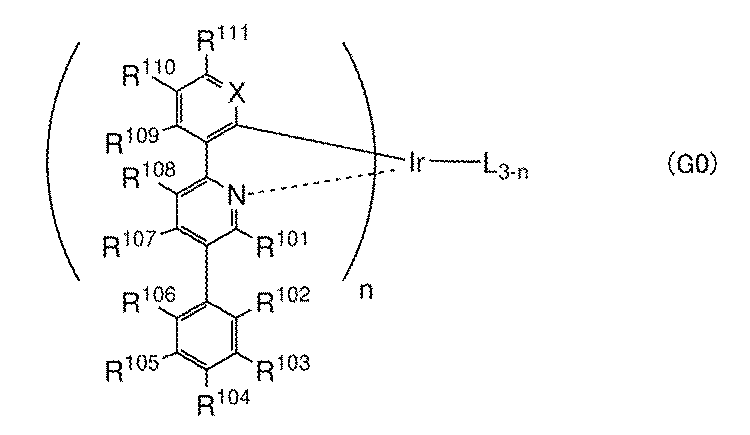

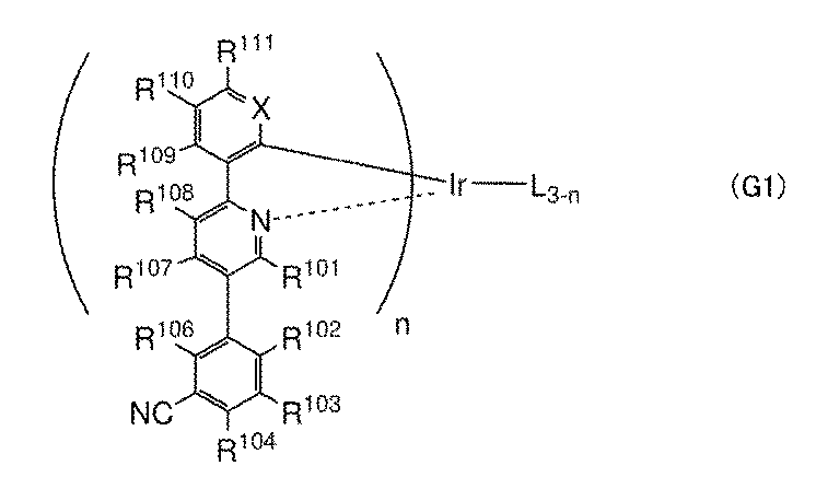
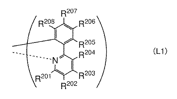

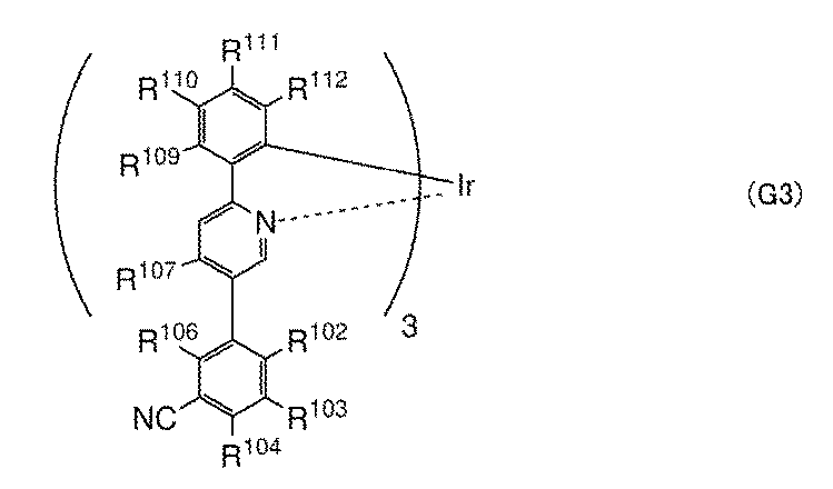

図2Aおよび図2Bは、実施の形態に係る発光デバイスの構成を説明する図である。
図3Aおよび図3Bは、実施の形態に係る表示装置の構成を説明する図である。
図4Aおよび図4Bは、実施の形態に係る表示装置の構成を説明する図である。
図5A乃至図5Cは、実施の形態に係る装置の構成を説明する図である。
図6は、実施の形態に係る装置の構成を説明する図である。
図7Aおよび図7Bは、実施の形態に係る装置の構成を説明する図である。
図8Aおよび図8Bは、実施の形態に係るアクティブマトリクス型発光装置の構成を説明する図である。
図9Aおよび図9Bは、実施の形態に係るアクティブマトリクス型発光装置の構成を説明する図である。
図10は、実施の形態に係るアクティブマトリクス型発光装置の構成を説明する図である。
図11Aおよび図11Bは、実施の形態に係るパッシブマトリクス型発光装置の構成を説明する図である。
図12Aおよび図12Bは、実施の形態に係る照明装置の構成を説明する図である。
図13A乃至図13Dは、実施の形態に係る電子機器の構成を説明する図である。
図14A乃至図14Cは、実施の形態に係る電子機器の構成を説明する図である。
図15は、実施の形態に係る照明装置の構成を説明する図である。
図16は、実施の形態に係る照明装置の構成を説明する図である。
図17は、実施の形態に係る車載表示装置および照明装置の構成を説明する図である。
図18A乃至図18Cは、実施の形態に係る電子機器の構成を説明する図である。
図19は、実施例に係る有機化合物のプロトンNMRスペクトルを説明する図である。
図20は、実施例に係る有機化合物の吸収スペクトルおよび発光スペクトルを説明する図である。
図21は、実施例に係る有機化合物のプロトンNMRスペクトルを説明する図である。
図22は、実施例に係る有機化合物の吸収スペクトルおよび発光スペクトルを説明する図である。
図23は、実施例に係る有機化合物のプロトンNMRスペクトルを説明する図である。
図24は、実施例に係る有機化合物の吸収スペクトルおよび発光スペクトルを説明する図である。
図25は、実施例に係る有機化合物のプロトンNMRスペクトルを説明する図である。
図26は、実施例に係る有機化合物の吸収スペクトルおよび発光スペクトルを説明する図である。
図27は、実施例に係る発光デバイスの構成を説明する図である。
図28は、実施例に係る発光デバイスの電流密度−輝度特性を説明する図である。
図29は、実施例に係る発光デバイスの輝度−電流効率特性を説明する図である。
図30は、実施例に係る発光デバイスの電圧−輝度特性を説明する図である。
図31は、実施例に係る発光デバイスの電圧−電流特性を説明する図である。
図32は、実施例に係る発光デバイスの輝度−外部量子効率特性を説明する図である。
図33は、実施例に係る発光デバイスの発光スペクトルを説明する図である。
図34は、実施例に係る発光デバイスの規格化輝度の経時変化を説明する図である。

本実施の形態では、本発明の一態様の有機化合物について説明する。
本実施の形態で説明する本発明の一態様の有機化合物は、一般式(G0)で表される。
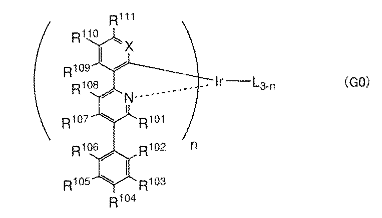
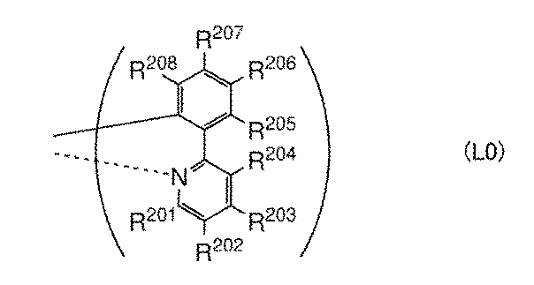
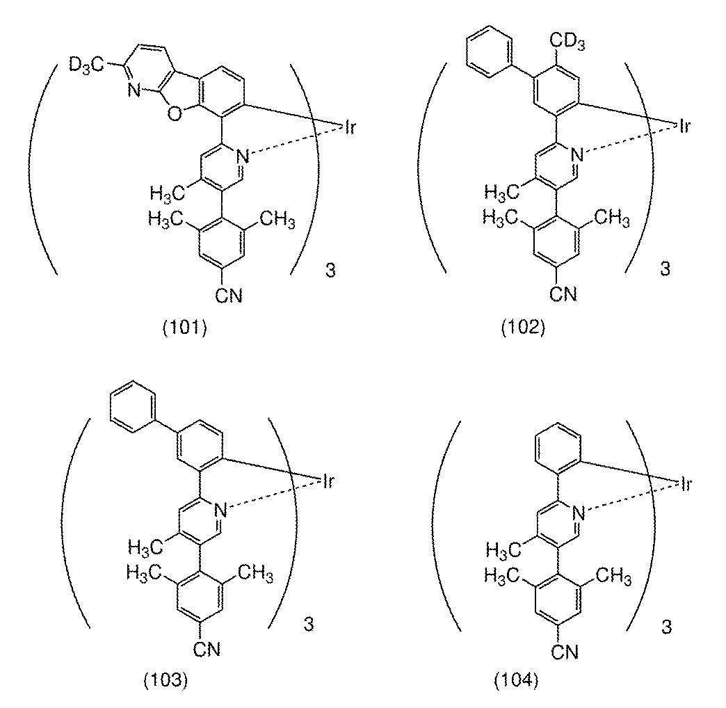
また、本発明の一態様の有機化合物は、一般式(G1)で表される。

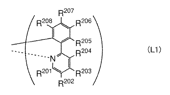

また、本発明の一態様の有機化合物は、一般式(G2)で表される。


また、本発明の一態様の有機化合物は、一般式(G3)で表される。
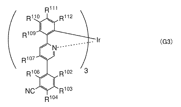
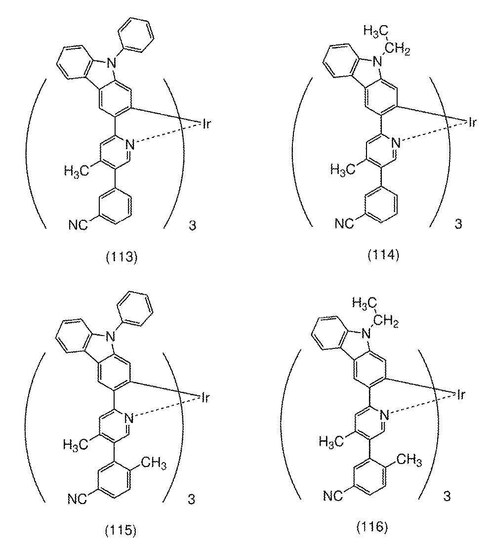

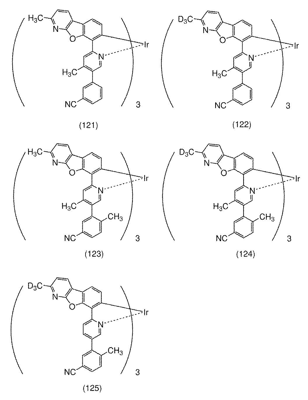


また、本発明の一態様の有機化合物は、一般式(G4)で表される。

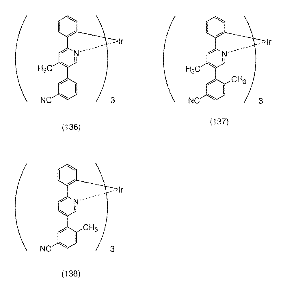
本発明の一態様の有機化合物の合成方法について説明する。なお、合成方法はこれに限定されない。他の合成方法または公知の合成方法を用いても合成することができる。
下記一般式(G0)で表される有機化合物は、以下のような合成スキーム(a)で示す方法により合成することができる。

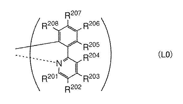


本実施の形態では、本発明の一態様の発光デバイス550Xの構成について、図1Aおよび図1Bを参照しながら説明する。
本実施の形態で説明する発光デバイス550Xは、電極551Xと、電極552Xと、ユニット103Xと、を有する。電極552Xは、電極551Xと重なり、ユニット103Xは、電極552Xおよび電極551Xの間に挟まれる。
ユニット103Xは単層構造または積層構造を備える。例えば、ユニット103Xは、層111X、層112および層113を備える(図1A参照)。ユニット103Xは光ELXを射出する機能を備える。
例えば、正孔輸送性を有する材料を、層112に用いることができる。また、層112を正孔輸送層ということができる。なお、層111Xに含まれる発光性の材料より大きいバンドギャップを備える材料を、層112に用いる構成が好ましい。これにより、層111Xにおいて生じる励起子から層112へのエネルギー移動を、抑制することができる。
正孔移動度が、1×10⁻⁶cm2/Vs以上である材料を、正孔輸送性を有する材料に好適に用いることができる。
例えば、電子輸送性を有する材料、アントラセン骨格を有する材料および混合材料等を、層113に用いることができる。また、層113を電子輸送層ということができる。なお、層111Xに含まれる発光性の材料より大きいバンドギャップを有する材料を、層113に用いる構成が好ましい。これにより、層111Xにおいて生じる励起子から層113へのエネルギー移動を、抑制することができる。
例えば、電界強度[V/cm]の平方根が600である条件において、電子移動度が1×10−7cm2/Vs以上、5×10−5cm2/Vs以下である材料を、電子輸送性を有する材料に好適に用いることができる。これにより、電子輸送層における電子の輸送性を抑制することができる。または、発光層への電子の注入量を制御することができる。または、発光層が電子過多の状態になることを防ぐことができる。
アントラセン骨格を有する有機化合物を、層113に用いることができる。特に、アントラセン骨格と複素環骨格の両方を含む有機化合物を好適に用いることができる。
また、複数種の物質を混合した材料を、層113に用いることができる。具体的には、アルカリ金属、アルカリ金属化合物またはアルカリ金属錯体と、電子輸送性を有する物質とを含む混合材料を、層113に用いることができる。なお、電子輸送性を有する材料の最高被占軌道(HOMO:Highest occupied molecular orbital)準位が−6.0eV以上であるとより好ましい。
例えば、発光性の材料、または発光性の材料およびホスト材料を、層111Xに用いることができる。また、層111Xを発光層ということができる。なお、正孔と電子が再結合する領域に層111Xを配置する構成が好ましい。これにより、キャリアの再結合により生じるエネルギーを、効率よく光にして射出することができる。
りん光発光物質を層111Xに用いることができる。例えば、実施の形態1において説明する本発明の一態様の有機化合物を層111Xに用いることができる。
キャリア輸送性を備える材料をホスト材料に用いることができる。例えば、正孔輸送性を有する材料、電子輸送性を有する材料、熱活性化遅延蛍光(TADF:Thermally Activated Delayed Fluorescence)を示す物質、アントラセン骨格を有する材料およびこれらから選ばれる2以上の混合材料等をホスト材料に用いることができる。なお、層111Xに含まれる発光性の材料より大きいバンドギャップを備える材料を、ホスト材料に用いる構成が好ましい。これにより、層111Xにおいて生じる励起子からホスト材料へのエネルギー移動を、抑制することができる。
正孔移動度が、1×10⁻⁶cm2/Vs以上である材料を、正孔輸送性を有する材料に好適に用いることができる。例えば、層112に用いることができる正孔輸送性を有する材料を、ホスト材料に用いることができる。
金属錯体またはπ電子不足型複素芳香環骨格を有する有機化合物を、電子輸送性を有する材料に用いることができる。例えば、層113に用いることができる電子輸送性を有する材料を、ホスト材料に用いることができる。
また、複数種の物質を混合した材料を、ホスト材料に用いることができる。例えば、電子輸送性を有する材料と正孔輸送性を有する材料を、混合材料に用いることができる。混合材料に含まれる正孔輸送性を有する材料と電子輸送性を有する材料の重量比の値は、(正孔輸送性を有する材料/電子輸送性を有する材料)=(1/19)以上(19/1)以下とすればよい。これにより、層111Xのキャリア輸送性を容易に調整することができる。また、再結合領域の制御も簡便に行うことができる。
本発明の一態様の有機化合物を、ホスト材料に用いることができる。本発明の一態様の有機化合物はりん光発光物質であり、りん光発光物質は、発光物質として蛍光発光物質を用いる際に蛍光発光物質へ励起エネルギーを供与するエネルギードナーとして用いることができる。
励起錯体を形成する材料を含む混合材料を、ホスト材料に用いることができる。例えば、形成される励起錯体の発光スペクトルが、発光物質の最も低エネルギー側の吸収帯の波長と重なる材料を、ホスト材料に用いることができる。具体的には、電子輸送性を有する材料と正孔輸送性を有する材料を含む混合材料を、励起錯体を形成する材料に用いることができる。これにより、エネルギー移動がスムーズとなり、発光効率を向上することができる。または、駆動電圧を抑制することができる。このような構成とすることにより、励起錯体から発光物質(燐光材料)へのエネルギー移動であるExTET(Exciplex−Triplet Energy Transfer)を用いた発光を効率よく得ることができる。
本実施の形態では、本発明の一態様の発光デバイス550Xの構成について、図1Aおよび図1Bを参照しながら説明する。
本実施の形態で説明する発光デバイス550Xは、電極551Xと、電極552Xと、ユニット103Xと、層104と、を有する。電極552Xは、電極551Xと重なり、ユニット103Xは、電極551Xおよび電極552Xの間に挟まれる。また、層104は、電極551Xおよびユニット103Xの間に挟まれる。なお、例えば、実施の形態2において説明する構成を、ユニット103Xに用いることができる。
例えば、導電性材料を電極551Xに用いることができる。具体的には、金属、合金または導電性化合物を含む膜を、単層または積層で電極551Xに用いることができる。
例えば、正孔注入性を有する材料を、層104に用いることができる。また、層104を正孔注入層ということができる。
具体的には、電子受容性を有する物質を、層104に用いることができる。または、複数種の物質を含む複合材料を、層104に用いることができる。これにより、正孔を、例えば、電極551Xから注入しやすくすることができる。または、発光デバイス550Xの駆動電圧を小さくすることができる。
有機化合物および無機化合物を、電子受容性を有する物質に用いることができる。電子受容性を有する物質は、電界の印加により、隣接する正孔輸送層あるいは正孔輸送性を有する材料から電子を引き抜くことができる。
また、例えば、電子受容性を有する物質と正孔輸送性を有する材料を含む複合材料を層104に用いることができる。これにより、仕事関数が大きい材料だけでなく、仕事関数の小さい材料を電極551Xに用いることができる。または、仕事関数に依らず、広い範囲の材料から、電極551Xに用いる材料を選ぶことができる。
例えば、電子受容性を有する物質と、正孔輸送性を有する材料と、アルカリ金属のフッ化物またはアルカリ土類金属のフッ化物とを、含む複合材料を、正孔注入性を有する材料に用いることができる。特に、原子比率において、フッ素原子が20%以上である複合材料を好適に用いることができる。これにより、層104の屈折率を低下させることができる。または、発光デバイス550Xの内部に屈折率の低い層を形成することができる。または、発光デバイス550Xの外部量子効率を向上することができる。
本実施の形態では、本発明の一態様の発光デバイス550Xの構成について、図1Aおよび図1Bを参照しながら説明する。
本実施の形態で説明する発光デバイス550Xは、電極551Xと、電極552Xと、ユニット103Xと、層105と、を有する。電極552Xは、電極551Xと重なる領域を備え、ユニット103Xは、電極551Xおよび電極552Xの間に挟まれる領域を備える。また、層105は、ユニット103Xおよび電極552Xの間に挟まれる領域を備える。なお、例えば、実施の形態2において説明する構成を、ユニット103Xに用いることができる。
例えば、導電性材料を電極552Xに用いることができる。具体的には、金属、合金または導電性化合物を含む材料を、単層または積層で電極552Xに用いることができる。
例えば、電子注入性を有する材料を、層105に用いることができる。また、層105を電子注入層ということができる。
例えば、アルカリ金属、アルカリ土類金属、希土類金属またはこれらの化合物(酸化物、ハロゲン化物、炭酸塩等)を、電子供与性を有する物質に用いることができる。または、テトラチアナフタセン(略称:TTN)、ニッケロセン、デカメチルニッケロセン等の有機化合物を、電子供与性を有する物質に用いることもできる。
また、複数種の物質を複合した材料を、電子注入性を有する材料に用いることができる。例えば、電子供与性を有する物質と電子輸送性を有する材料を、複合材料に用いることができる。
例えば、電界強度V/cmの平方根が600である条件において、電子移動度が1×10−7cm2/Vs以上、5×10−5cm2/Vs以下である材料を、電子輸送性を有する材料に好適に用いることができる。これにより、発光層への電子の注入量を制御することができる。または、発光層が電子過多の状態になることを防ぐことができる。
また、微結晶状態のアルカリ金属のフッ化物と電子輸送性を有する材料を、複合材料に用いることができる。または、微結晶状態のアルカリ土類金属のフッ化物と電子輸送性を有する材料を、複合材料に用いることができる。特に、アルカリ金属のフッ化物またはアルカリ土類金属のフッ化物を50wt%以上含む複合材料を好適に用いることができる。または、ビピリジン骨格を有する有機化合物を含む複合材料を好適に用いることができる。これにより、層105の屈折率を低下することができる。または、発光デバイス550Xの外部量子効率を向上することができる。
例えば、非共有電子対を備える第1の有機化合物および第1の金属を含む複合材料を、層105に用いることができる。また、第1の有機化合物の電子数と第1の金属の電子数の合計が奇数であると好ましい。また、第1の有機化合物1モルに対する第1の金属のモル比率は、好ましくは0.1以上10以下、より好ましくは0.2以上2以下、さらに好ましくは0.2以上0.8以下である。
例えば、電子輸送性を有する材料を、非共有電子対を備える有機化合物に用いることができる。例えば、電子不足型複素芳香環を有する化合物を用いることができる。具体的には、ピリジン環、ジアジン環(ピリミジン環、ピラジン環、ピリダジン環)、トリアジン環の少なくとも一つを有する化合物を用いることができる。これにより、発光デバイス550Xの駆動電圧を低減することができる。
例えば、非共有電子対を備える第1の有機化合物の電子数が偶数である場合、周期表における奇数の族である金属および第1の有機化合物の複合材料を、層105に用いることができる。
例えば、カルシウムとアルミニウムの混合酸化物に電子を高濃度添加した物質等を、電子注入性を有する材料に用いることができる。
本実施の形態では、本発明の一態様の発光デバイス550Xの構成について、図2Aを参照しながら説明する。
また、本実施の形態で説明する発光デバイス550Xは、電極551Xと、電極552Xと、ユニット103Xと、層106と、を有する(図2A参照)。電極552Xは、電極551Xと重なる領域を備え、ユニット103Xは、電極551Xおよび電極552Xの間に挟まれる領域を備える。層106は、電極552Xおよびユニット103Xの間に挟まれる領域を備える。
層106は、電圧を加えることにより、陽極側に電子を供給し、陰極側に正孔を供給する機能を備える。また、層106を電荷発生層ということができる。
層106_1および層106_2を積層した積層膜を、層106に用いることができる。層106_1は、ユニット103Xおよび電極552Xの間に挟まれる領域を備え、層106_2は、ユニット103Xおよび層106_1の間に挟まれる領域を備える。
例えば、実施の形態3において説明する層104に用いることができる正孔注入性を有する材料を層106_1に用いることができる。具体的には、複合材料を層106_1に用いることができる。また、1×10⁴[Ω・cm]以上1×10⁷[Ω・cm]以下の電気抵抗率を備える膜を、層106_1に用いることができる。また、好ましくは、層106_1は、5×10⁴[Ω・cm]以上1×10⁷[Ω・cm]以下の電気抵抗率を備え、より好ましくは、1×10⁵[Ω・cm]以上1×10⁷[Ω・cm]以下の電気抵抗率を備える。
例えば、実施の形態4において説明する層105に用いることができる材料を、層106_2に用いることができる。
層106_1、層106_2および層106_3を積層した積層膜を、層106に用いることができる。層106_3は、層106_1および層106_2の間に挟まれる領域を備える。
例えば、電子輸送性を有する材料を層106_3に用いることができる。また、層106_3を電子リレー層ということができる。層106_3を用いると、層106_3の陽極側に接する層を、層106_3の陰極側に接する層から遠ざけることができる。層106_3の陽極側に接する層と、層106_3の陰極側に接する層の間の相互作用を軽減することができる。層106_3の陽極側に接する層に電子をスムーズに供給することができる。
本実施の形態では、本発明の一態様の発光デバイス550Xの構成について、図2Bを参照しながら説明する。
本実施の形態で説明する発光デバイス550Xは、電極551Xと、電極552Xと、ユニット103Xと、層106と、ユニット103X2と、を有する(図2B参照)。
ユニット103X2は、層111X2、層112_2および層113_2を備える。層111X2は、層112_2および層113_2の間に挟まれる。
また、ユニット103Xとは異なる構成をユニット103X2に用いることができる。例えば、ユニット103Xの発光色とは色相が異なる光を射出する構成を、ユニット103X2に用いることができる。
層106は、ユニット103Xまたはユニット103X2の一方に電子を供給し、他方に正孔を供給する機能を備える。例えば、実施の形態5において説明する層106を用いることができる。
例えば、乾式法、湿式法、蒸着法、液滴吐出法、塗布法または印刷法等を用いて、電極551X、電極552X、ユニット103X、層106、およびユニット103X2の各層を形成することができる。また、異なる方法を各構成の形成に用いることができる。
本実施の形態では、本発明の一態様の表示装置700の構成について、図3Aおよび図3Bを参照しながら説明する。
本実施の形態で説明する表示装置700は、発光デバイス550X(i,j)と、発光デバイス550Y(i,j)と、を有する(図3A参照)。発光デバイス550Y(i,j)は、発光デバイス550X(i,j)と隣接する。
発光デバイス550X(i,j)は、電極551X(i,j)と、電極552X(i,j)と、ユニット103X(i,j)と、を有する。電極552X(i,j)は電極551X(i,j)と重なり、ユニット103X(i,j)は、電極552X(i,j)および電極551X(i,j)の間に挟まれる。また、発光デバイス550X(i,j)は層104X(i,j)および層105X(i,j)を有し、層104X(i,j)はユニット103X(i,j)および電極551X(i,j)の間に挟まれ、層105X(i,j)は電極552X(i,j)およびユニット103X(i,j)の間に挟まれる。なお、ユニット103X(i,j)は層111X(i,j)、層112X(i,j)および層113X(i,j)を備える。
発光デバイス550Y(i,j)は、電極551Y(i,j)と、電極552Y(i,j)と、ユニット103Y(i,j)と、を有する。電極552Y(i,j)は電極551Y(i,j)と重なり、ユニット103Y(i,j)は、電極552Y(i,j)および電極551Y(i,j)の間に挟まれる。また、発光デバイス550Y(i,j)は層104Y(i,j)および層105Y(i,j)を有し、層104Y(i,j)はユニット103Y(i,j)および電極551Y(i,j)の間に挟まれ、層105Y(i,j)は電極552Y(i,j)およびユニット103Y(i,j)の間に挟まれる。
発光デバイス550Y(i,j)は、層111Y(i,j)の構成が発光デバイス550X(i,j)とは異なる。ここでは、異なる部分について詳細に説明し、同じ構成を備える部分については、上記の説明を援用する。
例えば、発光性の材料、または発光性の材料およびホスト材料を、層111Y(i,j)に用いることができる。また、層111Y(i,j)を発光層ということができる。なお、正孔と電子が再結合する領域に層111Y(i,j)を配置する構成が好ましい。これにより、キャリアの再結合により生じるエネルギーを、効率よく光にして射出することができる。
蛍光発光物質を層111Y(i,j)に用いることができる。例えば、以下に例示する蛍光発光物質を層111Y(i,j)に用いることができる。なお、これに限定されず、さまざまな公知の蛍光性発光物質を層111Y(i,j)に用いることができる。
りん光発光物質を層111Y(i,j)に用いることができる。例えば、以下に例示するりん光発光物質を層111Y(i,j)に用いることができる。なお、これに限定されず、さまざまな公知のりん光性発光物質を層111Y(i,j)に用いることができる。
4H−トリアゾール骨格を有する有機金属イリジウム錯体等としては、例えば、トリス{2−[5−(2−メチルフェニル)−4−(2,6−ジメチルフェニル)−4H−1,2,4−トリアゾール−3−イル−κN2]フェニル−κC}イリジウム(III)(略称:[Ir(mpptz−dmp)3])、トリス(5−メチル−3,4−ジフェニル−4H−1,2,4−トリアゾラト)イリジウム(III)(略称:[Ir(Mptz)3])、トリス[4−(3−ビフェニル)−5−イソプロピル−3−フェニル−4H−1,2,4−トリアゾラト]イリジウム(III)(略称:[Ir(iPrptz−3b)3])、等を用いることができる。
ピリミジン骨格を有する有機金属イリジウム錯体等としては、例えば、トリス(4−メチル−6−フェニルピリミジナト)イリジウム(III)(略称:[Ir(mppm)3])、トリス(4−t−ブチル−6−フェニルピリミジナト)イリジウム(III)(略称:[Ir(tBuppm)3])、(アセチルアセトナト)ビス(6−メチル−4−フェニルピリミジナト)イリジウム(III)(略称:[Ir(mppm)2(acac)])、(アセチルアセトナト)ビス(6−tert−ブチル−4−フェニルピリミジナト)イリジウム(III)(略称:[Ir(tBuppm)2(acac)])、(アセチルアセトナト)ビス[6−(2−ノルボルニル)−4−フェニルピリミジナト]イリジウム(III)(略称:[Ir(nbppm)2(acac)])、(アセチルアセトナト)ビス[5−メチル−6−(2−メチルフェニル)−4−フェニルピリミジナト]イリジウム(III)(略称:[Ir(mpmppm)2(acac)])、(アセチルアセトナト)ビス(4,6−ジフェニルピリミジナト)イリジウム(III)(略称:[Ir(dppm)2(acac)])、等を用いることができる。
ピリミジン骨格を有する有機金属イリジウム錯体等としては、例えば、(ジイソブチリルメタナト)ビス[4,6−ビス(3−メチルフェニル)ピリミジナト]イリジウム(III)(略称:[Ir(5mdppm)2(dibm)])、ビス[4,6−ビス(3−メチルフェニル)ピリミジナト](ジピバロイルメタナト)イリジウム(III)(略称:[Ir(5mdppm)2(dpm)])、ビス[4,6−ジ(ナフタレン−1−イル)ピリミジナト](ジピバロイルメタナト)イリジウム(III)(略称:[Ir(d1npm)2(dpm)])、等を用いることができる。
TADF材料を層111Y(i,j)に用いることができる。TADF材料を発光物質として用いる場合、ホスト材料のS1準位はTADF材料のS1準位より高い方が好ましい。また、ホスト材料のT1準位はTADF材料のT1準位より高いことが好ましい。


キャリア輸送性を備える材料をホスト材料に用いることができる。例えば、正孔輸送性を有する材料、電子輸送性を有する材料、熱活性化遅延蛍光(TADF:Thermally Activated Delayed Fluorescence)を示す物質、アントラセン骨格を有する材料および混合材料等をホスト材料に用いることができる。なお、層111Y(i,j)に含まれる発光性の材料より大きいバンドギャップを備える材料を、ホスト材料に用いる構成が好ましい。これにより、層111Y(i,j)において生じる励起子からホスト材料へのエネルギー移動を、抑制することができる。
正孔移動度が、1×10⁻⁶cm2/Vs以上である材料を、正孔輸送性を有する材料に好適に用いることができる。例えば、層112に用いることができる正孔輸送性を有する材料を、ホスト材料に用いることができる。
金属錯体またはπ電子不足型複素芳香環骨格を有する有機化合物を、電子輸送性を有する材料に用いることができる。例えば、層113に用いることができる電子輸送性を有する材料を、ホスト材料に用いることができる。
アントラセン骨格を有する有機化合物を、ホスト材料に用いることができる。特に、発光物質に蛍光発光物質を用いる場合において、アントラセン骨格を有する有機化合物は好適である。これにより、発光効率および耐久性が良好な発光デバイスを実現することができる。
TADF材料をホスト材料に用いることができる。TADF材料をホスト材料に用いると、TADF材料で生成した三重項励起エネルギーを、逆項間交差によって一重項励起エネルギーに変換することができる。さらに、励起エネルギーを発光物質に移動することができる。換言すれば、TADF材料はエネルギードナーとして機能し、発光物質はエネルギーアクセプターとして機能する。これにより、発光デバイスの発光効率を高めることができる。
また、複数種の物質を混合した材料を、ホスト材料に用いることができる。例えば、電子輸送性を有する材料と正孔輸送性を有する材料を、混合材料に用いることができる。混合材料に含まれる正孔輸送性を有する材料と電子輸送性を有する材料の重量比の値は、(正孔輸送性を有する材料/電子輸送性を有する材料)=(1/19)以上(19/1)以下とすればよい。これにより、層111Y(i,j)のキャリア輸送性を容易に調整することができる。また、再結合領域の制御も簡便に行うことができる。
りん光発光物質を混合した材料を、ホスト材料に用いることができる。りん光発光物質は、発光物質として蛍光発光物質を用いる際に蛍光発光物質へ励起エネルギーを供与するエネルギードナーとして用いることができる。
励起錯体を形成する材料を含む混合材料を、ホスト材料に用いることができる。例えば、形成される励起錯体の発光スペクトルが、発光物質の最も低エネルギー側の吸収帯の波長と重なる材料を、ホスト材料に用いることができる。これにより、エネルギー移動がスムーズとなり、発光効率を向上することができる。または、駆動電圧を抑制することができる。このような構成とすることにより、励起錯体から発光物質(燐光材料)へのエネルギー移動であるExTET(Exciplex−Triplet Energy Transfer)を用いた発光を効率よく得ることができる。
また、本実施の形態で説明する表示装置700は、絶縁膜528を有する(図3A参照)。
絶縁膜528は開口部を備え、一の開口部は電極551X(i,j)と重なり、他の開口部は電極551Y(i,j)と重なる。また、絶縁膜528は間隙551XY(i,j)と重なる。
電極551X(i,j)および電極551Y(i,j)の間に挟まれる間隙551XY(i,j)は、例えば、溝状の形状を備える。これにより、当該溝に沿って段差が形成される。また、間隙551XY(i,j)上に堆積する膜と、電極551X(i,j)上に堆積する膜との間に、断絶または膜厚が薄い部分が形成される。
本実施の形態で説明する表示装置700は、発光デバイス550X(i,j)と、発光デバイス550Y(i,j)と、を有する(図3B参照)。発光デバイス550Y(i,j)は、発光デバイス550X(i,j)と隣接する。
膜529_1は開口部を備え、一の開口部は電極551X(i,j)と重なり、他の開口部は電極551Y(i,j)と重なる(図3B参照)。また、膜529_1は間隙551XY(i,j)と重なる開口部を備える。例えば、金属、金属酸化物、有機材料または無機絶縁材料を含む膜を、膜529_1に用いることができる。具体的には、遮光性の金属膜を用いることができる。これにより、発光デバイスの構成を、加工工程において照射される光から、保護することができる。
膜529_2は開口部を備え、一の開口部は電極551X(i,j)と重なり、他の開口部は電極551Y(i,j)と重なる。また、膜529_2は間隙551XY(i,j)と重なる。
膜529_3は開口部を備え、一の開口部は電極551X(i,j)と重なり、他の開口部は電極551Y(i,j)と重なる。また、膜529_3は、間隙551XY(i,j)と重なる領域に形成される溝を埋める。例えば、感光性樹脂を用いて膜529_3を形成することができる。具体的には、アクリル樹脂などを用いることができる。
本実施の形態では、本発明の一態様の表示装置700の構成について、図4Aおよび図4Bを参照しながら説明する。
本実施の形態で説明する表示装置700は、発光デバイス550X(i,j)と、光電変換デバイス550S(i,j)とを有する(図4A参照)。光電変換デバイス550S(i,j)は、発光デバイス550X(i,j)と隣接する。
発光デバイス550X(i,j)は、電極551X(i,j)と、電極552X(i,j)と、ユニット103X(i,j)と、を有する。電極552X(i,j)は電極551X(i,j)と重なり、ユニット103X(i,j)は、電極552X(i,j)および電極551X(i,j)の間に挟まれる。また、発光デバイス550X(i,j)は層104X(i,j)および層105X(i,j)を有し、層104X(i,j)はユニット103X(i,j)および電極551X(i,j)の間に挟まれ、層105X(i,j)は電極552X(i,j)およびユニット103X(i,j)の間に挟まれる。
光電変換デバイス550S(i,j)は、電極551S(i,j)と、電極552S(i,j)と、ユニット103S(i,j)と、を有する。電極552S(i,j)は電極551S(i,j)と重なり、ユニット103S(i,j)は、電極552S(i,j)および電極551S(i,j)の間に挟まれる。また、光電変換デバイス550S(i,j)は層104S(i,j)および層105S(i,j)を有し、層104S(i,j)はユニット103S(i,j)および電極551S(i,j)の間に挟まれ、層105S(i,j)は電極552S(i,j)およびユニット103S(i,j)の間に挟まれる。
ユニット103S(i,j)は単層構造または積層構造を備える。例えば、光電変換層の他、正孔輸送層、電子輸送層、キャリアブロック層、などの機能層から選択した層を、ユニット103S(i,j)に用いることができる。
層114S(i,j)を光電変換層ということができる。層114S(i,j)は光hvを吸収し、一方に接する層に電子を、他方に接する層に正孔を供給する。例えば、層114S(i,j)は層112に正孔を、層113に電子を供給する。例えば、有機太陽電池に用いることができる材料を、層114S(i,j)に用いることができる。具体的には、電子受容性の材料および電子供与性の材料を、層114S(i,j)に用いることができる。
例えば、フラーレン誘導体、非フラーレン電子受容体等を電子受容性の材料に用いることができる。
例えば、フタロシアニン化合物、テトラセン誘導体、キナクリドン誘導体、ルブレン誘導体、等を電子供与性の材料に用いることができる。
例えば、単層構造または積層構造を層114S(i,j)に用いることができる。具体的には、バルクヘテロ接合型の構造を層114S(i,j)に用いることができる。または、ヘテロ接合型の構造を層114S(i,j)に用いることができる。
例えば、電子受容性の材料および電子供与性の材料を含む混合材料を層114S(i,j)に用いることができる(図4A参照)。なお、電子受容性の材料および電子供与性の材料を含む混合材料を層114S(i,j)に用いる構成をバルクヘテロ接合型ということができる。
層114N(i,j)および層114P(i,j)を層114S(i,j)に用いることができる(図4B参照)。層114N(i,j)は一方の電極および層114P(i,j)の間に挟まれ、層114P(i,j)は層114N(i,j)および他方の電極の間に挟まれる。例えば、層114N(i,j)は電極552S(i,j)および層114P(i,j)の間に挟まれ、層114P(i,j)は層114N(i,j)および電極551S(i,j)の間に挟まれる。
本実施の形態では、本発明の一態様の装置の構成について、図5乃至図7を参照しながら説明する。
本発明の一態様の表示装置700は、領域231を有する(図5A参照)。領域231は、一組の画素703(i,j)を備える。
一組の画素703(i,j)は、画素702X(i,j)を備える(図5Bおよび図5C参照)。
また、本発明の一態様の表示装置700は、機能層540と、機能層520と、を有する(図5C参照)。機能層540は機能層520と重なる。
また、本発明の一態様の表示装置700は、駆動回路GDおよび駆動回路SDを有する(図5A参照)。
駆動回路GDは、第1の選択信号および第2の選択信号を供給する。
駆動回路SDは、第1の制御信号および第2の制御信号を供給する。
配線は、導電膜G1(i)、導電膜G2(i)、導電膜S1(j)、導電膜S2(j)、導電膜ANO、導電膜VCOM2および導電膜V0を含む(図6参照)。
画素回路530X(i,j)は、導電膜G1(i)および導電膜S1(j)と電気的に接続される。導電膜G1(i)は第1の選択信号を供給し、導電膜S1(j)は、第1の制御信号を供給する。
画素回路530X(i,j)は、スイッチSW21、スイッチSW22、トランジスタM21、容量C21およびノードN21を備える。
画素回路530X(i,j)は、スイッチSW23、ノードN22および容量C22を備える。
画素702X(i,j)は、発光デバイス550X(i,j)および画素回路530X(i,j)を備える(図7A参照)。機能層540は発光デバイス550X(i,j)および着色層CFXを含み、機能層520は画素回路530X(i,j)を含む。
図7Bを用いて説明する画素702X(i,j)は、ボトムエミッション型の発光デバイスを備える。発光デバイス550X(i,j)は光ELXを機能層520が配置されている側に射出する。
本実施の形態では、実施の形態2乃至実施の形態6のいずれか一に記載の発光デバイスを用いた発光装置について説明する。
本実施の形態では、実施の形態2乃至実施の形態6のいずれか一に記載の発光デバイスを照明装置として用いる例を、図12を参照しながら説明する。図12Bは照明装置の上面図、図12Aは図12Bにおけるe−f断面図である。
本実施の形態では、実施の形態2乃至実施の形態6のいずれか一に記載の発光デバイスをその一部に含む電子機器の例について説明する。実施の形態2乃至実施の形態6のいずれか一に記載の発光デバイスは発光効率が良好であり、消費電力の小さい発光デバイスである。その結果、本実施の形態に記載の電子機器は、消費電力が小さい発光部を有する電子機器とすることが可能である。
本合成例1では、実施の形態1において構造式(136)で示す、トリス[2−(4−メチル−5−(3−シアノフェニル)−2−ピリジニル−κN)フェニル−κC]イリジウム(III)(略称:Ir(mppy−3CP)3)の合成方法の一例を説明する。
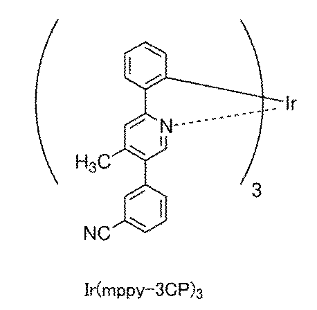
5−ブロモ−4−メチル−2−フェニルピリジン2.36gと、3−シアノフェニルボロン酸1.77gと、リン酸三カリウム2.54gと、トルエン35mLと、水3.5mLとを、還流管を付けた三口フラスコに入れ、内部を窒素置換した。フラスコ内を減圧下で撹拌することで脱気した後、トリス(ジベンジリデンアセトン)ジパラジウム(0)(略称:Pd2(dba)3)0.089gと、2−ジシクロヘキシルホスフィノ−2’,6’−ジメトキシビフェニル(略称:S−Phos)0.16gと、を加えた。攪拌しながら、110℃で7.5時間反応させた。ステップ1の合成スキーム(1a)を以下に示す。

上記ステップ1で得た4−メチル−2−フェニル−5−(3−シアノフェニル)ピリジン(略称:Hmppy−3CP)2.42gと、トリス(2,4−ペンタンジオナト)イリジウム(III)(略称:Ir(acac)3)0.88gとを、三方コックを付けた反応容器に入れ、反応容器内をアルゴン置換した。撹拌しながら、250℃で71時間反応させた。ステップ2の合成スキーム(1b)を以下に示す。
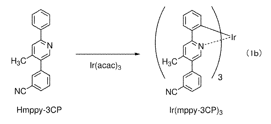
本合成例2では、実施の形態1において構造式(104)で示す、トリス[2−(4−メチル−5−(4−シアノ−2,6−ジメチルフェニル)−2−ピリジニル−κN)フェニル−κC]イリジウム(III)(略称:Ir(mppy−dmCP)3)の合成方法の一例を説明する。
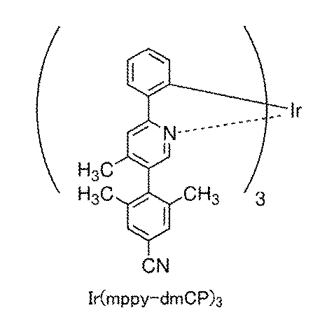
2,5−ジブロモ−4−メチルピリジン15.87gと、フェニルボロン酸9.27gと、炭酸カリウム23.51gと、アセトニトリル530mLと、メタノール265mLとを、還流管を付けた三口フラスコに入れ、内部を窒素置換した。フラスコ内を減圧下で撹拌することで脱気した後、酢酸ジパラジウム(II)(略称:Pd(OAc)2)0.56gと、トリフェニルホスフィン(略称:PPh3)1.65gとを、加えた。撹拌しながら、50℃で19.5時間反応させた。ステップ1の合成スキーム(2a)を以下に示す。

上記ステップ1で得た5−ブロモ−4−メチル−2−フェニルピリジン3.25gと、3,5−ジメチル−4−(4,4,5,5−テトラメチル−1,3,2−ジオキサボロラン−2−イル)ベンゾニトリル4.09gと、リン酸三カリウム10.96gと、2−ジシクロヘキシルホスフィノ−2’,6’−ジメトキシビフェニル(略称:S−Phos)4.13gと、トルエン160mLとを、還流管を付けた三口フラスコに入れ、内部を窒素置換した。フラスコ内を減圧下で撹拌することで脱気した後、トリス(ジベンジリデンアセトン)ジパラジウム(0)(略称:Pd2(dba)3)2.25gを加えた。攪拌しながら、130℃で15時間反応させた。ステップ2の合成スキーム(2b)を以下に示す。

2−エトキシエタノール15mLと水5mL、ステップ2で得た4−メチル−2−フェニル−5−(4−シアノ−2,6−ジメチルフェニル)ピリジン(略称:Hmppy−dmCP)2.01gと、塩化イリジウム水和物(IrCl3・H2O)(フルヤ金属社製)0.99gとを、還流管を付けたナスフラスコに入れ、フラスコ内をアルゴン置換した。その後、このフラスコに、2.45GHzのマイクロ波を100Wの出力で2時間照射して、反応させた。ステップ3の合成スキーム(2c)を以下に示す。

ステップ3で得たジ−μ−クロロ−テトラキス[2−(4−メチル−5−(4−シアノ−2,6−ジメチルフェニル)−2−ピリジニル−κN)フェニル−κC]ジイリジウム(III)(略称:[Ir(mppy−dmCP)2Cl]2)1.82gと、ステップ2で得た4−メチル−2−フェニル−5−(4−シアノ−2,6−ジメチルフェニル)ピリジン(略称:Hmppy−dmCP)1.70gと、炭酸カリウム1.51gと、フェノール8gとを、還流管を付けた三口フラスコに入れ、内部を窒素置換した。その後、攪拌しながら、185℃で24時間反応させた。ステップ4の合成スキーム(2d)を以下に示す。
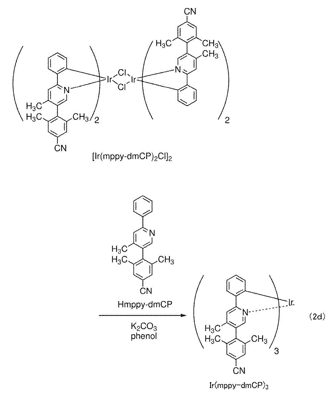
本合成例3では、実施の形態1の構造式(137)で表される本発明の有機金属錯体、トリス[2−(4−メチル−5−(5−シアノ−2−メチルフェニル)−2−ピリジニル−κN)フェニル−κC]イリジウム(III)(略称:Ir(mppy−m5CP)3)の合成方法を説明する。
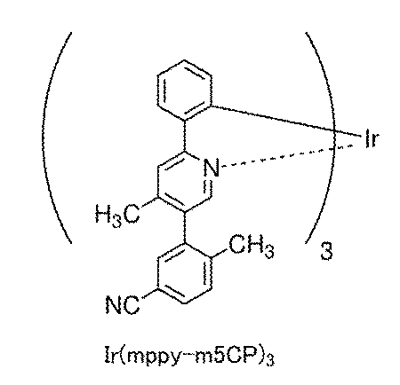
5−ブロモ−4−メチル−2−フェニルピリジン2.31gと、5−シアノ−2−フェニルボロン酸2.23gと、リン酸三カリウム7.88gと、トルエン115mLとを、還流管を付けた三口フラスコに入れ、内部を窒素置換した。フラスコ内を減圧下で撹拌することで脱気した後、トリス(ジベンジリデンアセトン)ジパラジウム(0)(略称:Pd2(dba)3)1.08gと、2−ジシクロヘキシルホスフィノ−2’,6’−ジメトキシビフェニル(略称:S−Phos)2.01gとを加えた。撹拌しながら、130℃で7.5時間反応させた。ステップ1の合成スキーム(3a)を以下に示す。
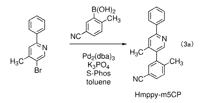
上記ステップ1で得た4−メチル−2−フェニル−5−(5−シアノ−2−メチルフェニル)ピリジン(略称:Hmppy−m5CP)2.42gと、トリス(2,4−ペンタンジオナト)イリジウム(III)(略称:Ir(acac)3)0.88gとを、三方コックを付けた反応容器に入れ、反応容器内をアルゴン置換した。攪拌しながら、250℃で67.5時間反応させた。ステップ2の合成スキーム(3b)を以下に示す。
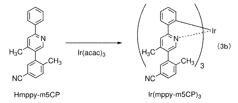
本合成例4では、実施の形態1において構造式(138)で示す、トリス[2−(5−(5−シアノ−2−メチルフェニル)−2−ピリジニル−κN)フェニル−κC]イリジウム(III)(略称:Ir(ppy−m5CP)3)の合成方法の一例を説明する。

5−ブロモ−2−メチルピリジン9.82gと、5−シアノ−2−メチルフェニルボロン酸8.03gと、リン酸三カリウム10.62gと、トルエン150mLと、水15mLとを、還流管を付けた三口フラスコに入れ、内部を窒素置換した。フラスコ内を減圧下で撹拌することで脱気した後、トリス(ジベンジリデンアセトン)ジパラジウム(0)(略称:Pd2(dba)3)0.38gと、2−ジシクロヘキシルホスフィノ−2’,6’−ジメトキシビフェニル(略称:S−Phos)0.70gと、を加えた。攪拌しながら、110℃で2時間反応させた。ステップ1の合成スキーム(4a)を以下に示す。
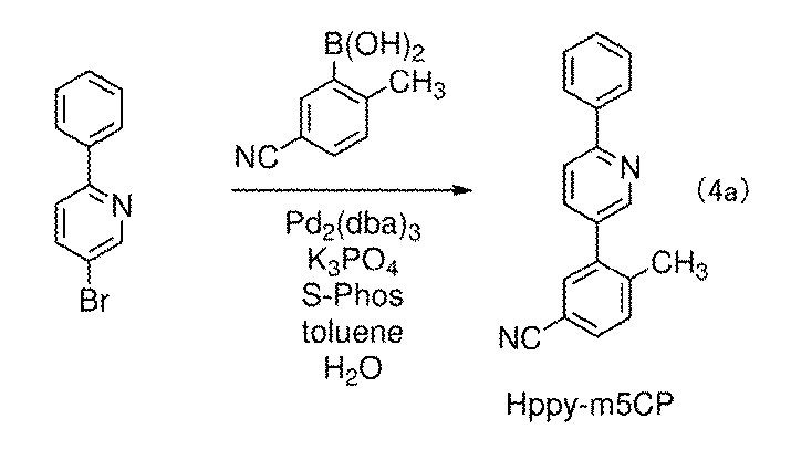
上記ステップ1で得た5−(5−シアノ−2−メチルフェニル)−2−フェニルピリジン(略称:Hppy−m5CP)2.22gと、トリス(2,4−ペンタンジオナト)イリジウム(III)(略称:Ir(acac)3)0.78gとを、三方コックを付けた反応容器に入れ、反応容器内をアルゴン置換した。攪拌しながら、250℃で78時間反応させた。ステップ2の合成スキーム(4b)を以下に示す。
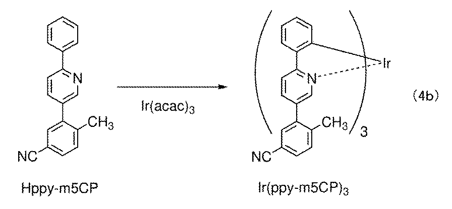
本実施例で説明する作製した発光デバイス1は、発光デバイス550Xと同様の構成を備える(図27参照)。
発光デバイス1の構成を表1に示す。また、本実施例で説明する発光デバイスに用いた材料の構造式を以下に示す。なお、本実施例の表中において、下付き文字および上付き文字は、便宜上、標準の大きさで記載される。例えば、略称に用いる下付き文字および単位に用いる上付き文字は、表中において、標準の大きさで記載される。表中のこれらの記載は、明細書の記載を参酌して読み替えることができる。


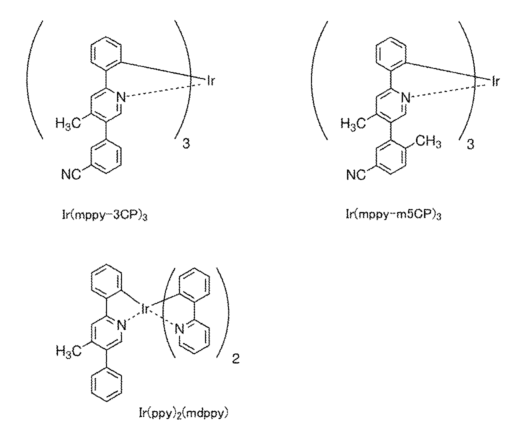
下記のステップを有する方法を用いて、本実施例で説明する発光デバイス1を作製した。
第1のステップにおいて、電極551Xを形成した。具体的には、ターゲットにケイ素もしくは酸化ケイ素を含有した酸化インジウム−酸化スズ(略称:ITSO)を用いて、スパッタリング法により形成した。なお、電極551XはITSOを含み、70nmの厚さと、4mm2(2mm×2mm)の面積を備える。
第2のステップにおいて、電極551X上に層104Xを形成した。具体的には、抵抗加熱法を用いて材料を共蒸着した。なお、層104Xは4,4’,4’’−(ベンゼン−1,3,5−トリイル)トリ(ジベンゾチオフェン)(略称:DBT3P−II)および酸化モリブデン(略称:MoOx)を、DBT3P−II:MoOx=2:1(重量比)で含み、40nmの厚さを備える。
第3のステップにおいて、層104X上に層112Xを形成した。具体的には、抵抗加熱法を用いて材料を蒸着した。なお、層112Xは4,4’−ジフェニル−4’’−(9−フェニル−9H−カルバゾール−3−イル)トリフェニルアミン(略称:PCBBi1BP)を含み、20nmの厚さを備える。
第4のステップにおいて、層112X上に層111Xを形成した。具体的には、抵抗加熱法を用いて材料を共蒸着した。なお、層111Xは9−[3−(4,6−ジフェニル−1,3,5−トリアジン−2−イル)フェニル]−9’−フェニル−2,3’−ビ−9H−カルバゾール(略称:mPCCzPTzn−02)、9,9’−ジフェニル−9H,9’H−3,3’−ビカルバゾール(略称:PCCP)およびトリス[2−(4−メチル−5−(3−シアノフェニル)−2−ピリジニルーκN)フェニル−κC]イリジウム(III)(略称:Ir(mppy−3CP)3)を、mPCCzPTzn−02:PCCP:Ir(mppy−3CP)3=0.6:0.4:0.1(重量比)で含み、40nmの厚さを備える。
第5のステップにおいて、層111X上に層113X1を形成した。具体的には、抵抗加熱法を用いて材料を蒸着した。なお、層113X1はmPCCzPTzn−02を含み、20nmの厚さを備える。
第6のステップにおいて、層113X1上に層113X2を形成した。具体的には、抵抗加熱法を用いて材料を蒸着した。なお、層113X2は2,9−ジ(2−ナフチル)−4,7−ジフェニル−1,10−フェナントロリン(略称:NBphen)を含み、10nmの厚さを備える。
第7のステップにおいて、層113X2上に層105Xを形成した。具体的には、抵抗加熱法を用いて材料を蒸着した。なお、層105Xはフッ化リチウム(LiF)を含み、1nmの厚さを備える。
第8のステップにおいて、層105X上に電極552Xを形成した。具体的には、抵抗加熱法を用いて材料を蒸着した。なお、電極552Xはアルミニウム(Al)を含み、200nmの厚さを備える。
電力を供給すると発光デバイス1は光EL1を射出した(図27参照)。発光デバイス1の動作特性を、室温(23℃)にて測定した(図28乃至図33参照)。なお、輝度およびCIE色度の測定には、色彩輝度計(トプコン社製、BM−5A)を用い、発光スペクトルの測定には、マルチチャンネル分光器(浜松フォトニクス社製、PMA−11)を用いた。
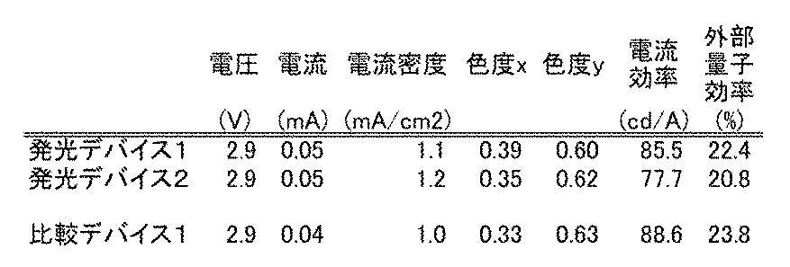

本実施例で説明する作製した発光デバイス2は、発光デバイス550Xと同様の構成を備える(図27参照)。発光デバイス2の構成は、層111Xにおいて発光デバイス1と異なる。具体的には、層111Xが、Ir(mppy−3CP)3に換えてトリス[2−(4−メチル−5−(5−シアノ−2−メチルフェニル)−2−ピリジニル−κN)フェニル−κC]イリジウム(III)(略称:Ir(mppy−m5CP)3)を含む点が発光デバイス1とは異なる。
下記のステップを有する方法を用いて、本実施例で説明する発光デバイス2を作製した。
第4のステップにおいて、層112X上に層111Xを形成した。具体的には、抵抗加熱法を用いて材料を共蒸着した。なお、層111XはmPCCzPTzn−02、PCCPおよびIr(mppy−m5CP)3を、mPCCzPTzn−02:PCCP:Ir(mppy−m5CP)3=0.6:0.4:0.1(重量比)で含み、40nmの厚さを備える。
電力を供給すると発光デバイス1、発光デバイス2は光EL1を射出した(図27参照)。発光デバイス2の動作特性を、室温にて測定した(図28乃至図33参照)。
本参考例で説明する作製した比較デバイス1は、発光デバイス550Xと同様の構成を備える(図27参照)。
比較デバイス1の構成は、層111Xにおいて発光デバイス1と異なる。具体的には、層111Xが、Ir(mppy−3CP)3に換えて[2−(4−メチル−5−フェニル−2−ピリジニル−κN)フェニル−κC]ビス[2−(2−ピリジニル−κN)フェニル−κC]イリジウム(III)(略称:Ir(ppy)2(mdppy))を含む点が発光デバイス1とは異なる。
下記のステップを有する方法を用いて、本実施例で説明する比較デバイス1を作製した。
第4のステップにおいて、層112X上に層111Xを形成した。具体的には、抵抗加熱法を用いて材料を共蒸着した。なお、層111XはmPCCzPTzn−02、PCCPおよびIr(ppy)2(mdppy)を、mPCCzPTzn−02:PCCP:Ir(ppy)2(mdppy)=0.6:0.4:0.1(重量比)で含み、40nmの厚さを備える。
電力を供給すると比較デバイス1は光EL1を射出した(図27参照)。比較デバイス1の動作特性を、室温にて測定した(図28乃至図33参照)。
Claims (8)
- 一般式(G0)で表される有機化合物。

Xは、窒素原子または炭素原子であり、
Xが炭素原子であるとき、Xは、水素または置換基と結合し、
R104およびR105のいずれか一方は、シアノ基であり、
R102およびR107の少なくとも一は、炭素数1乃至6のアルキル基であり、
R101乃至R111の他は、それぞれ独立に、水素または置換基と結合し、
前記置換基は、それぞれ独立に、炭素数1乃至6のアルキル基、炭素数3乃至7のシクロアルキル基、置換もしくは無置換の炭素数6乃至13のアリール基、置換もしくは無置換の炭素数1乃至5のヘテロアリール基、アミノ基またはヒドロキシ基であり、
前記置換基は、互いに結合して環を形成してもよく、
nは、1以上3以下の整数であり、
Lは、構造式(L0)で表される配位子であり、
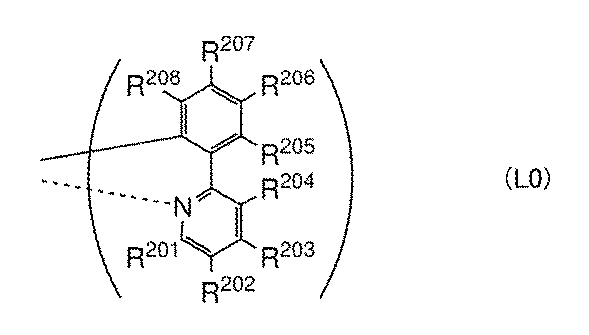
R201乃至R208は、それぞれ独立に、水素または炭素数1乃至6のアルキル基であり、
また、一般式(G0)において、水素はいずれも重水素であってもよい。 - 一般式(G1)で表される有機化合物。

Xは、窒素原子または炭素原子であり、
Xが炭素原子であるとき、Xは、水素または置換基と結合し、
R102およびR107の少なくとも一は、炭素数1乃至6のアルキル基であり、
R101乃至R111の他は、それぞれ独立に、水素または置換基と結合し、
前記置換基は、それぞれ独立に、炭素数1乃至6のアルキル基、炭素数3乃至7のシクロアルキル基、置換もしくは無置換の炭素数6乃至13のアリール基、置換もしくは無置換の炭素数1乃至5のヘテロアリール基、アミノ基またはヒドロキシ基であり、
前記置換基は、互いに結合して環を形成してもよく、
nは、1以上3以下の整数であり、
Lは、構造式(L1)で表される配位子であり、
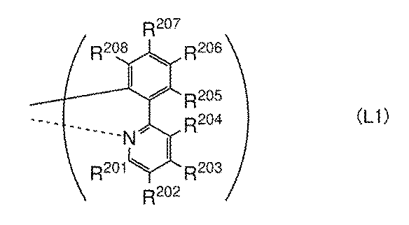
R201乃至R208は、それぞれ独立に、水素または炭素数1乃至6のアルキル基であり、
また、一般式(G1)において、水素はいずれも重水素であってもよい。 - 一般式(G2)で表される有機化合物。

R102およびR107の少なくとも一は、炭素数1乃至6のアルキル基であり、
R102乃至R112の他は、それぞれ独立に、水素または置換基と結合し、
前記置換基は、それぞれ独立に、炭素数1乃至6のアルキル基、炭素数3乃至7のシクロアルキル基、置換もしくは無置換の炭素数6乃至13のアリール基、置換もしくは無置換の炭素数1乃至5のヘテロアリール基、アミノ基またはヒドロキシ基であり、
前記置換基は、互いに結合して環を形成してもよく、
また、一般式(G2)において、水素はいずれも重水素であってもよい。 - 一般式(G3)で表される有機化合物。

R102およびR107の少なくとも一は、炭素数1乃至6のアルキル基であり、
R102乃至R112の他は、それぞれ独立に、水素または置換基と結合し、
前記置換基は、それぞれ独立に、炭素数1乃至6のアルキル基、炭素数3乃至7のシクロアルキル基、置換もしくは無置換の炭素数6乃至13のアリール基、置換もしくは無置換の炭素数1乃至5のヘテロアリール基、アミノ基またはヒドロキシ基であり、
前記置換基は、互いに結合して環を形成してもよく、
また、一般式(G3)において、水素はいずれも重水素であってもよい。 - 一般式(G4)で表される有機化合物。
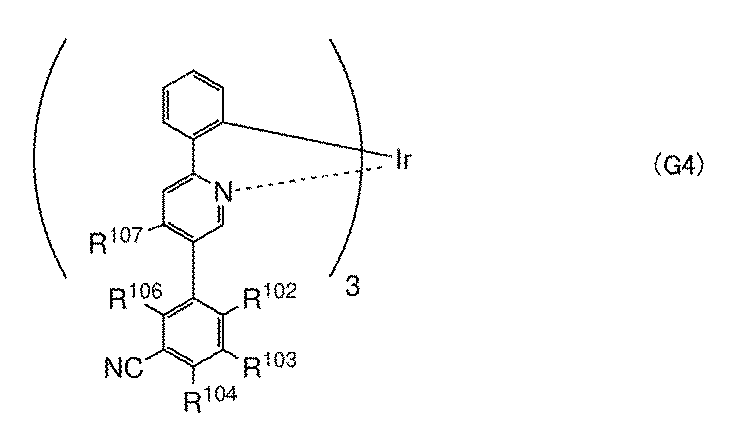
R102およびR107の少なくとも一は、炭素数1乃至6のアルキル基であり、
R102乃至R107の他は、それぞれ独立に、水素または置換基と結合し、
前記置換基は、それぞれ独立に、炭素数1乃至6のアルキル基、炭素数3乃至7のシクロアルキル基、置換もしくは無置換の炭素数6乃至13のアリール基、置換もしくは無置換の炭素数1乃至5のヘテロアリール基、アミノ基またはヒドロキシ基であり、
前記置換基は、互いに結合して環を形成してもよく、
また、一般式(G4)において、水素はいずれも重水素であってもよい。 - 第1の電極と、
第2の電極と、
第1のユニットと、を有し、
前記第1のユニットは、第1の電極および第2の電極の間に挟まれ、
前記第1のユニットは、請求項1乃至請求項5のいずれか一に記載の有機化合物を含む、発光デバイス。 - 第1の発光デバイスと、
第2の発光デバイスと、を有し、
前記第1の発光デバイスは、第3の電極、第4の電極、第2のユニットおよび第1の層を備え、
前記第2のユニットは、前記第3の電極および前記第4の電極の間に挟まれ、
前記第1の層は、前記第2のユニットおよび前記第3の電極の間に挟まれ、
前記第2のユニットは、請求項1乃至請求項5のいずれか一に記載の有機化合物を含み、
前記第1の層は、ハロゲン基もしくはシアノ基を含む第2の有機化合物または遷移金属酸化物を含み、
前記第2の発光デバイスは、前記第1の発光デバイスと隣接し、
前記第2の発光デバイスは、第5の電極、第6の電極、第3のユニットおよび第2の層を備え、
前記第5の電極は、前記第3の電極との間に、間隙を備え、
前記第3のユニットは、前記第6の電極および前記第5の電極の間に挟まれ、
前記第3のユニットは、発光性の材料を含み、
前記第2の層は、前記第3のユニットおよび前記第5の電極の間に挟まれ、
前記第2の層は、前記第2の有機化合物または前記遷移金属酸化物を含み、
前記第2の層は、前記第1の層との間に、前記第1の層より膜厚が薄い領域を備え、
前記領域は、前記間隙と重なる、表示装置。 - 第1の機能層と、
第2の機能層と、を有し、
前記第1の機能層は、前記第2の機能層と重なり、
前記第1の機能層は、第1の画素回路および第2の画素回路を含み、
前記第2の機能層は、第1の発光デバイスおよび第2の発光デバイスを含み、
前記第1の発光デバイスは、第3の電極、第4の電極および第2のユニットを備え、
前記第2のユニットは、前記第3の電極および前記第4の電極の間に挟まれ、
前記第2のユニットは、請求項1乃至請求項5のいずれか一に記載の有機化合物を含み、
前記第3の電極は、前記第1の画素回路と電気的に接続され、
前記第2の発光デバイスは、第5の電極、第6の電極および第3のユニットを備え、
前記第3のユニットは、前記第5の電極および前記第6の電極の間に挟まれ、
前記第5の電極は、前記第2の画素回路と電気的に接続され、
前記第6の電極は、前記第4の電極と電気的に接続される、表示装置。
Priority Applications (4)
| Application Number | Priority Date | Filing Date | Title |
|---|---|---|---|
| CN202380033028.2A CN119403813A (zh) | 2022-04-15 | 2023-03-31 | 有机化合物、发光器件、显示装置 |
| JP2024515173A JPWO2023199152A1 (ja) | 2022-04-15 | 2023-03-31 | |
| US18/856,290 US20250255172A1 (en) | 2022-04-15 | 2023-03-31 | Organic Compound, Light-Emitting Device, and Display Apparatus |
| KR1020247033385A KR20250005096A (ko) | 2022-04-15 | 2023-03-31 | 유기 화합물, 발광 디바이스, 표시 장치 |
Applications Claiming Priority (2)
| Application Number | Priority Date | Filing Date | Title |
|---|---|---|---|
| JP2022067292 | 2022-04-15 | ||
| JP2022-067292 | 2022-04-15 |
Publications (1)
| Publication Number | Publication Date |
|---|---|
| WO2023199152A1 true WO2023199152A1 (ja) | 2023-10-19 |
Family
ID=88329152
Family Applications (1)
| Application Number | Title | Priority Date | Filing Date |
|---|---|---|---|
| PCT/IB2023/053221 Ceased WO2023199152A1 (ja) | 2022-04-15 | 2023-03-31 | 有機化合物、発光デバイス、表示装置 |
Country Status (5)
| Country | Link |
|---|---|
| US (1) | US20250255172A1 (ja) |
| JP (1) | JPWO2023199152A1 (ja) |
| KR (1) | KR20250005096A (ja) |
| CN (1) | CN119403813A (ja) |
| WO (1) | WO2023199152A1 (ja) |
Citations (2)
| Publication number | Priority date | Publication date | Assignee | Title |
|---|---|---|---|---|
| JP2012502046A (ja) * | 2008-09-03 | 2012-01-26 | ユニバーサル ディスプレイ コーポレイション | リン光性材料 |
| KR20120032054A (ko) * | 2010-07-28 | 2012-04-05 | 롬엔드하스전자재료코리아유한회사 | 신규한 유기 발광 화합물 및 이를 포함하는 유기 전계 발광 소자 |
-
2023
- 2023-03-31 WO PCT/IB2023/053221 patent/WO2023199152A1/ja not_active Ceased
- 2023-03-31 CN CN202380033028.2A patent/CN119403813A/zh active Pending
- 2023-03-31 US US18/856,290 patent/US20250255172A1/en active Pending
- 2023-03-31 JP JP2024515173A patent/JPWO2023199152A1/ja active Pending
- 2023-03-31 KR KR1020247033385A patent/KR20250005096A/ko active Pending
Patent Citations (2)
| Publication number | Priority date | Publication date | Assignee | Title |
|---|---|---|---|---|
| JP2012502046A (ja) * | 2008-09-03 | 2012-01-26 | ユニバーサル ディスプレイ コーポレイション | リン光性材料 |
| KR20120032054A (ko) * | 2010-07-28 | 2012-04-05 | 롬엔드하스전자재료코리아유한회사 | 신규한 유기 발광 화합물 및 이를 포함하는 유기 전계 발광 소자 |
Also Published As
| Publication number | Publication date |
|---|---|
| JPWO2023199152A1 (ja) | 2023-10-19 |
| US20250255172A1 (en) | 2025-08-07 |
| CN119403813A (zh) | 2025-02-07 |
| KR20250005096A (ko) | 2025-01-09 |
Similar Documents
| Publication | Publication Date | Title |
|---|---|---|
| JP7846177B2 (ja) | 有機化合物、発光デバイス、電子機器、発光装置および照明装置 | |
| JP7608544B2 (ja) | 発光素子、発光装置、電子機器、及び照明装置 | |
| JP7822132B2 (ja) | 発光デバイス、発光装置、電子機器および照明装置 | |
| JP2026063235A (ja) | 発光デバイス | |
| WO2023062474A1 (ja) | 発光デバイス、表示装置、電子機器、発光装置、照明装置 | |
| JP2022066170A (ja) | 有機化合物、発光デバイス、発光装置、電子機器、表示装置、照明装置 | |
| JP2025116098A (ja) | 発光デバイス、電子機器、発光装置および照明装置 | |
| JP2024040235A (ja) | 有機化合物、elデバイスおよび電子デバイス | |
| JP2023174743A (ja) | 蒸着用組成物 | |
| JP2021175719A (ja) | 有機金属錯体、トップエミッション用発光材料、発光デバイス、発光装置、電子機器および照明装置 | |
| JP7808950B2 (ja) | 発光デバイス、発光装置、電子機器、表示装置、照明装置 | |
| JP7634945B2 (ja) | 有機化合物及び発光デバイス | |
| JP7626601B2 (ja) | 有機化合物、発光デバイス、発光装置、電子機器および照明装置 | |
| JP2023103975A (ja) | 発光デバイス、表示装置、電子機器、発光装置、照明装置 | |
| KR20220044658A (ko) | 발광 디바이스, 에너지 도너 재료, 발광 장치, 표시 장치, 조명 장치, 및 전자 기기 | |
| WO2022053905A1 (ja) | 有機金属錯体、発光デバイス、発光装置、電子機器、および照明装置 | |
| US20250255172A1 (en) | Organic Compound, Light-Emitting Device, and Display Apparatus | |
| US20230250119A1 (en) | Organic Compound, Light-Emitting Device, Display Device, Electronic Device, Light-Emitting Apparatus, and Lighting Device | |
| KR20240021118A (ko) | 유기 화합물, 발광 디바이스, 표시 장치, 전자 기기,발광 장치, 조명 장치 | |
| WO2023175442A1 (ja) | 表示装置、電子機器 | |
| JP2023020998A (ja) | 有機化合物、発光デバイス、表示装置、電子機器、発光装置、照明装置 | |
| JP2023004936A (ja) | 発光デバイス、光電変換デバイス、表示装置、発光装置 | |
| WO2022162508A1 (ja) | 発光デバイス、発光装置、電子機器、表示装置、照明装置 | |
| JP2025109756A (ja) | 発光デバイス |
Legal Events
| Date | Code | Title | Description |
|---|---|---|---|
| 121 | Ep: the epo has been informed by wipo that ep was designated in this application |
Ref document number: 23787888 Country of ref document: EP Kind code of ref document: A1 |
|
| ENP | Entry into the national phase |
Ref document number: 2024515173 Country of ref document: JP Kind code of ref document: A |
|
| WWE | Wipo information: entry into national phase |
Ref document number: 202380033028.2 Country of ref document: CN |
|
| WWE | Wipo information: entry into national phase |
Ref document number: 18856290 Country of ref document: US |
|
| NENP | Non-entry into the national phase |
Ref country code: DE |
|
| WWP | Wipo information: published in national office |
Ref document number: 202380033028.2 Country of ref document: CN |
|
| 122 | Ep: pct application non-entry in european phase |
Ref document number: 23787888 Country of ref document: EP Kind code of ref document: A1 |
|
| WWP | Wipo information: published in national office |
Ref document number: 18856290 Country of ref document: US |