WO2023176472A1 - 電波反射板 - Google Patents
電波反射板 Download PDFInfo
- Publication number
- WO2023176472A1 WO2023176472A1 PCT/JP2023/007788 JP2023007788W WO2023176472A1 WO 2023176472 A1 WO2023176472 A1 WO 2023176472A1 JP 2023007788 W JP2023007788 W JP 2023007788W WO 2023176472 A1 WO2023176472 A1 WO 2023176472A1
- Authority
- WO
- WIPO (PCT)
- Prior art keywords
- radio wave
- wave reflecting
- reflecting plate
- plate according
- film
- Prior art date
- Legal status (The legal status is an assumption and is not a legal conclusion. Google has not performed a legal analysis and makes no representation as to the accuracy of the status listed.)
- Ceased
Links
Images


Classifications
-
- H—ELECTRICITY
- H01—ELECTRIC ELEMENTS
- H01Q—ANTENNAS, i.e. RADIO AERIALS
- H01Q3/00—Arrangements for changing or varying the orientation or the shape of the directional pattern of the waves radiated from an antenna or antenna system
- H01Q3/44—Arrangements for changing or varying the orientation or the shape of the directional pattern of the waves radiated from an antenna or antenna system varying the electric or magnetic characteristics of reflecting, refracting, or diffracting devices associated with the radiating element
-
- H—ELECTRICITY
- H01—ELECTRIC ELEMENTS
- H01Q—ANTENNAS, i.e. RADIO AERIALS
- H01Q15/00—Devices for reflection, refraction, diffraction or polarisation of waves radiated from an antenna, e.g. quasi-optical devices
- H01Q15/14—Reflecting surfaces; Equivalent structures
- H01Q15/148—Reflecting surfaces; Equivalent structures with means for varying the reflecting properties
-
- H—ELECTRICITY
- H01—ELECTRIC ELEMENTS
- H01Q—ANTENNAS, i.e. RADIO AERIALS
- H01Q15/00—Devices for reflection, refraction, diffraction or polarisation of waves radiated from an antenna, e.g. quasi-optical devices
- H01Q15/14—Reflecting surfaces; Equivalent structures
-
- H—ELECTRICITY
- H01—ELECTRIC ELEMENTS
- H01Q—ANTENNAS, i.e. RADIO AERIALS
- H01Q3/00—Arrangements for changing or varying the orientation or the shape of the directional pattern of the waves radiated from an antenna or antenna system
- H01Q3/44—Arrangements for changing or varying the orientation or the shape of the directional pattern of the waves radiated from an antenna or antenna system varying the electric or magnetic characteristics of reflecting, refracting, or diffracting devices associated with the radiating element
- H01Q3/46—Active lenses or reflecting arrays
-
- H—ELECTRICITY
- H01—ELECTRIC ELEMENTS
- H01Q—ANTENNAS, i.e. RADIO AERIALS
- H01Q17/00—Devices for absorbing waves radiated from an antenna; Combinations of such devices with active antenna elements or systems
- H01Q17/001—Devices for absorbing waves radiated from an antenna; Combinations of such devices with active antenna elements or systems for modifying the directional characteristic of an aerial
Definitions
- One embodiment of the present invention relates to a radio wave reflecting plate.
- liquid crystal molecules have dielectric constant anisotropy
- the dielectric constant of the liquid crystal layer can be controlled by adjusting the electric field applied to the liquid crystal layer containing liquid crystal molecules and controlling the orientation of the liquid crystal molecules.
- Patent Documents 1 and 2 disclose metasurfaces whose characteristics can be controlled by adjusting the electric field applied to the liquid crystal layer. By applying this technology, it is possible to construct a radio wave reflecting plate that is effective against radio waves of various wavelengths.
- An object of one embodiment of the present invention is to provide a radio wave reflecting plate having a new structure.
- one of the embodiments of the present invention aims to provide a large-sized radio wave reflecting plate.
- This radio wave reflection plate includes a plurality of radio wave reflection devices, an adjustment substrate on the plurality of radio wave reflection devices, and an antireflection film that is located on the adjustment substrate and absorbs radio waves.
- Each of the plurality of radio wave reflection devices includes a pair of substrates and a plurality of radio wave reflection elements between the pair of substrates.
- the antireflection film has a lattice shape as a whole. In each of the plurality of radio wave reflecting devices, an end portion is covered with an antireflection film, and a portion surrounded by the end portion is exposed from the antireflection film.
- One embodiment of the present invention is a method for manufacturing a radio wave reflecting plate.
- This manufacturing method includes arranging a plurality of radio wave reflection devices in a matrix, arranging an adjustment substrate on the plurality of radio wave reflection devices, and arranging an antireflection film on the adjustment substrate.
- Each of the plurality of radio wave reflection devices includes a pair of substrates and a plurality of radio wave reflection elements between the pair of substrates.
- the antireflection film has a lattice shape as a whole.
- the anti-reflection film is disposed in each of the plurality of radio wave reflecting devices such that the end portion is covered with the anti-reflection film and the portion surrounded by the end portion is exposed from the anti-reflection film.
- FIG. 1 is a schematic perspective view of a radio wave reflecting plate according to one embodiment of the present invention.
- FIG. 1 is a schematic development view of a radio wave reflecting plate according to one embodiment of the present invention.
- FIG. 1 is a schematic top view of a radio wave reflecting plate according to one embodiment of the present invention.
- FIG. 1 is a schematic top view of a radio wave reflecting plate according to one embodiment of the present invention.
- FIG. 2 is a schematic bottom view of a radio wave reflecting device included in a radio wave reflecting plate according to one embodiment of the present invention.
- FIG. 2 is a schematic top view of a radio wave reflecting element of a radio wave reflecting device included in a radio wave reflecting plate according to one embodiment of the present invention.
- FIG. 2 is a schematic end view of a radio wave reflecting element of a radio wave reflecting device included in a radio wave reflecting plate according to one embodiment of the present invention.
- FIG. 2 is a schematic top view of a portion of a radio wave reflecting plate according to one embodiment of the present invention.
- FIG. 2 is a schematic top view of a portion of a radio wave reflecting plate according to one embodiment of the present invention.
- FIG. 2 is a schematic top view of an antireflection film included in a radio wave reflecting plate according to one embodiment of the present invention.
- FIG. 2 is a schematic top view of an antireflection film included in a radio wave reflecting plate according to one embodiment of the present invention.
- FIG. 2 is a schematic top view of an antireflection film included in a radio wave reflecting plate according to one embodiment of the present invention.
- FIG. 2 is a schematic top view of an antireflection film included in a radio wave reflecting plate according to one embodiment of the present invention.
- FIG. 2 is a schematic top view of an antireflection film included in a radio wave reflecting plate according to one embodiment of the present invention.
- FIG. 2 is a schematic top view of an antireflection film included in a radio wave reflecting plate according to one embodiment of the present invention.
- FIG. 2 is a schematic top view of a portion of a radio wave reflecting plate according to one embodiment of the present invention.
- FIG. 2 is a schematic top view of an antireflection film included in a radio wave reflecting plate according to one embodiment of the present invention.
- FIG. 2 is a schematic end view of an antireflection film included in a radio wave reflecting plate according to one embodiment of the present invention.
- FIG. 2 is a schematic end view of a radio wave reflecting element included in a radio wave reflecting plate according to one embodiment of the present invention.
- FIG. 2 is a schematic end view of a radio wave reflecting element included in a radio wave reflecting plate according to one embodiment of the present invention.
- FIG. 2 is a schematic diagram illustrating the reflection of radio waves on a radio wave reflection plate in which a plurality of radio wave reflection devices are arranged.
- FIG. 2 is a schematic diagram illustrating reflection of radio waves on a radio wave reflecting plate according to one embodiment of the present invention.
- FIG. 2 is a schematic bottom view of a radio wave reflecting element of a radio wave reflecting device included in a radio wave reflecting plate according to one embodiment of the present invention.
- FIG. 2 is a schematic top view of a radio wave reflecting element of a radio wave reflecting device included in a radio wave reflecting plate according to one embodiment of the present invention.
- FIG. 2 is a schematic end view of a radio wave reflecting element of a radio wave reflecting device included in a radio wave reflecting plate according to one embodiment of the present invention.
- the term "on top” is used to indicate that the structure is in contact with a certain structure, unless otherwise specified. This includes both a case in which another structure is placed directly above a certain structure, and a case in which another structure is placed above a certain structure via another structure.
- a certain structure is exposed from another structure means that a part of a certain structure is not covered by another structure; The portion not covered by the body also includes embodiments covered by another structure.
- One embodiment of the present invention is a radio wave reflecting plate, and this radio wave reflecting plate has a function of reflecting irradiated radio waves in any direction.
- the wavelength of the radio waves may be in the range of 400 MHz to 50 GHz, and in this case, the radio wave reflector typically uses radio waves in the 400 MHz to 6.0 GHz band, 2.5 GHz to 4.7 GHz band, or 24 GHz to 50 GHz. Reflects radio waves from the band.
- a radio wave reflecting plate according to one embodiment of the present invention may be used as a reflecting plate for radio waves having a frequency exceeding 50 GHz.
- the radio wave reflection plate 100 basically includes a plurality of radio wave reflection devices 110, an adjustment substrate 106 on the plurality of radio wave reflection devices 110, and an antireflection film 104 on the adjustment substrate 106. .
- the adjustment substrate 106 and the antireflection film 104 are arranged so as to overlap the plurality of radio wave reflection devices 110.
- the radio wave reflecting plate 100 may further include a housing 102 and an adhesive layer 108.
- the view seen from the anti-reflection film 104 side is a top view
- the view seen from the opposite side to the anti-reflection film 104 is the bottom view
- the antireflection film 104 side is assumed to be the upper side
- the radio wave reflection device 110 side is assumed to be the lower side.
- the housing 102 is located under the plurality of radio wave reflecting devices 110 and is configured to accommodate the plurality of radio wave reflecting devices 110.
- the radio wave reflecting devices 110 are arranged within the housing 102 so as not to overlap each other.
- the casing 102 is a container containing metal, resin, or wood, and the plurality of radio wave reflecting devices 110 are exposed from the casing 102 by opening at least a portion of the top surface.
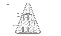
- the shape of the housing 102 is not limited to a rectangle as shown in FIG. 1, but may be a triangle as shown in FIG. 3A or a circle as shown in FIG. 3B.
- the shape of the housing 102 may be selected from various polygons including triangles and quadrangles, or may be an ellipse.
- the outline of the housing 102 may be composed of straight lines and curved lines.
- the radio wave reflection device 110 may be arranged in a matrix shape composed of a plurality of rows and columns. Can be done. In the example shown in FIG. 1, a plurality of radio wave reflecting devices 110 are arranged in a matrix of 4 rows and 4 columns.
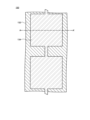
- Radio Wave Reflector (1) Structure A schematic bottom view of each radio wave reflector 110 is shown in FIG.
- the radio wave reflecting device 110 has a pair of substrates (only one substrate (second substrate 112) is shown in FIG. 4), and a plurality of radio wave reflecting elements 130 are arranged between the two substrates. Arranged in a matrix shape with rows and columns. There is no restriction on the number of radio wave reflecting elements 130, and the number of rows and columns are also arbitrary, and may be the same or different from each other.
- a surface formed by arranging a plurality of radio wave reflecting elements 130, that is, a single area (reflecting area) that simultaneously includes all radio wave reflecting elements 130, may be square, rectangular, or circular.
- the reflective region has one or more axes of symmetry across the reflective region.
- a pair of substrates including the second substrate 112 are fixed to each other by a sealing material 122 containing resin such as epoxy resin or acrylic resin.
- a liquid crystal layer 140 which will be described later, is sealed in a space formed by the pair of substrates and the sealing material 122.
- Wiring (not shown) extending from each radio wave reflecting element 130 is formed on the second substrate 112, and the wiring is exposed at the end of the second substrate 112 to form a terminal 114.
- the terminals 114 are connected to a drive circuit provided on a printed circuit board 118 by a connector 116 such as a flexible printed circuit (FPC) board.
- FPC flexible printed circuit
- signals and power for controlling the radio wave reflecting element 130 are supplied from the drive circuit to the radio wave reflecting element 130 via the connector 116, and the radio wave reflecting element 130 is controlled.
- the connector 116 is folded and arranged so that the second board 112 and the printed circuit board 118 overlap (see FIG. 2).
- the radio wave reflecting elements 130 can be arranged with high density within the housing 102.
- FIG. 5 shows a schematic top view of the radio wave reflection element 130
- FIG. 6 shows a schematic end view taken along the chain line AA' in FIG.
- two adjacent radio wave reflecting elements 130 are shown.
- each radio wave reflecting element 130 is provided between a pair of substrates, that is, the first substrate 120 and the second substrate 112.
- Each radio wave reflecting element 130 has a first electrode (also called a common electrode) 132 and a second electrode (also called a patch electrode) that are sandwiched between a first substrate 120 and a second substrate 112 and are opposed to each other.
- first alignment film 138 a second alignment film 142, and a liquid crystal layer 140 injected between the first alignment film 138 and the second alignment film 142 are provided. Note that for ease of viewing, only the first electrode 132 and the second electrode 134 are shown in FIG. 5.
- the first substrate 120 and the second substrate 112 are provided to provide physical strength to the radio wave reflecting device 110 and to provide a surface on which the radio wave reflecting element 130, wiring, etc. are arranged.
- First substrate 120 and/or second substrate 112 may be flexible.
- the first substrate 120 and the second substrate 112 may contain an inorganic insulator such as glass or quartz, a semiconductor such as silicon, a polymer such as polyimide, polycarbonate, or polyester, or a metal such as aluminum, copper, or stainless steel. I can do it.
- the surface on which the radio wave reflecting element 130 is provided that is, the second substrate 112 side of the first substrate 120
- Protective films 136 and 144 made of one or more films containing a silicon-containing inorganic compound such as silicon oxide or silicon nitride are provided on the surface of the second substrate 112 and the surface of the second substrate 112 on the first substrate 120 side, respectively. It is preferable. Note that since a film containing a silicon-containing inorganic compound has a high blocking property against impurities, the protective films 136 and 144 are provided even when the first substrate 120 and the second substrate 112 contain glass or a polymer. This can prevent impurities such as metal ions and water contained in the first substrate 120 and the second substrate 112 from entering the radio wave reflecting element 130.
- the first electrode 132 is provided on the first substrate 120. As described above, the first electrode 132 may be formed on the first substrate 120 with the protective film 136 having an arbitrary structure interposed therebetween. As shown in FIG. 5, in each radio wave reflecting device 110, the first electrode 132 can be provided over all the radio wave reflecting elements 130. That is, the first electrode 132 can be provided so as to be shared by all the radio wave reflecting elements 130. A constant potential is supplied to the first electrode 132 from a drive circuit on the printed circuit board 118 via the terminal 114 .
- the first electrode 132 is made of a metal such as copper, aluminum, tungsten, molybdenum, or titanium, an alloy containing at least one of these metals, or indium-tin oxide (ITO) or indium-zinc oxide (IZO). It may also contain conductive oxides such as.
- the first electrode 132 may also have a single layer structure, or may have a laminated structure in which layers of different compositions are laminated.
- the first electrode 132 may be formed using a sputtering method, a chemical vapor deposition (CVD) method, or the like.
- the first alignment film 138 and the second alignment film 142 are provided to control the alignment of liquid crystal molecules constituting the liquid crystal layer 140 provided between them. .
- a first alignment film 138 is disposed on the first electrode 132 and covers the first electrode 132.
- the second alignment film 142 is also provided under the second electrode 134 so as to overlap with the second electrode 134.
- the first alignment film 138 and the second alignment film 142 are continuously provided over the plurality of radio wave reflecting elements 130. In other words, the first alignment film 138 and the second alignment film 142 are not separated between adjacent radio wave reflection elements 130, but are shared by all radio wave reflection elements 130.
- the first alignment film 138 and the second alignment film 142 each contain a polymer such as polyimide or polyester, and are formed by using a wet film forming method such as an inkjet method, a spin coating method, a printing method, or a dip coating method. It is formed.
- the surfaces of the first alignment film 138 and the second alignment film 142 are subjected to a rubbing treatment.
- the direction of the rubbing process (rubbing direction) is the same between the first alignment film 138 and the second alignment film 142. Note that the rubbing direction is the orientation direction of the alignment film, and is the direction in which the long axes of liquid crystal molecules are aligned when they come into contact with the alignment film.
- the liquid crystal layer 140 includes liquid crystal molecules.
- the structure of liquid crystal molecules is not limited. Therefore, the liquid crystal molecules may be nematic liquid crystals, or may be smectic liquid crystals, cholesteric liquid crystals, or chiral smectic liquid crystals.
- the liquid crystal layer 140 is injected into the space formed by the first substrate 120, the second substrate 112, and the sealant 122, and is in direct contact with the first alignment film 138 and the second alignment film 142.
- the thickness of the liquid crystal layer 140 is, for example, 20 ⁇ m or more and 100 ⁇ m or less, or 30 ⁇ m or more and 50 ⁇ m or less. Therefore, the height of the sealant 122 is also selected within this range.
- spacers may be provided within the liquid crystal layer 140 in order to maintain this thickness throughout the radio wave reflecting plate 100. Note that if the thickness of the liquid crystal layer 140 described above is adopted in a liquid crystal display device, it will not be possible to obtain the high responsiveness necessary for displaying moving images, and it will be extremely difficult to perform the function as a liquid crystal display device. becomes.
- the second electrode 134 is provided on the second substrate 112 (under the second substrate 112 in FIG. 6). As an optional configuration, the second electrode 134 may be formed on the second substrate 112 with a protective film 144 interposed therebetween. As shown in FIG. 5, in the radio wave reflecting device 110, the second electrodes 134 of the radio wave reflecting elements 130 adjacent in the column direction or the row direction are electrically connected to each other and conductive. Therefore, for example, the second electrodes 134 of a plurality of radio wave reflecting elements 130 arranged in one column are electrically connected to each other and have an equal potential, but in this case, these second electrodes 134 are arranged in another column. It is not electrically connected to the second electrode 134 of the radio wave reflecting element 130. Similarly, when the second electrodes 134 of the plurality of radio wave reflecting elements 130 arranged in one row are electrically connected to each other and have an equal potential, these second electrodes 134 are It is not electrically connected to the second electrode 134 of the reflective element 130.
- the second electrode 134 is made of, for example, a metal such as copper, aluminum, tungsten, molybdenum, or titanium, an alloy containing at least one of these metals, or indium-tin oxide (ITO). and conductive oxides such as indium-zinc oxide (IZO).
- the second electrode 134 may also have a single layer structure, or may have a laminated structure in which layers of different compositions are laminated.
- the second electrode 134 may also be formed by applying a sputtering method, a CVD method, or the like.
- the first electrode 132 to which a common potential is applied across the plurality of radio wave reflecting elements 130 is arranged on the first substrate 120 side, and the second electrode 132 to which the same potential is applied to each column or row is disposed on the first substrate 120 side.
- An electrode 134 is arranged on the second substrate 112 side.
- the first electrode 132 to which a common potential is applied across the plurality of radio wave reflecting elements 130 is arranged on the second substrate 112 side, and the second electrode 134 to which the same potential is applied to each column or row. may be placed on the first substrate 120 side.
- the adjustment substrate 106 is provided on the second substrate 112 directly or via the adhesive layer 108 (see FIG. 2).
- materials included in the adhesive layer 108 include polymers such as epoxy resin and acrylic resin.
- the adjustment substrate 106 includes, for example, an inorganic compound such as glass or quartz, or a polymer such as polyimide, polyamide, or polycycloolefin. Although details will be described later, the radio waves incident on the radio wave reflection plate 100 pass through the adjustment substrate 106 and the second substrate 112 in order and reach the radio wave reflection element 130.
- the radio wave reflecting plate 100 can reflect radio waves at a reflection angle different from the incident angle. At this time, the incident wave and the reflected wave interfere with each other and strengthen each other, thereby preventing loss of radio wave intensity and reflecting the radio wave more efficiently.
- the thicknesses of the adjustment substrate 106, the adhesive layer 108, and the second substrate 112 are adjusted so that the optical distance of the one closest to the wavelength ⁇ (that is, the second substrate 112) is 1/4 ⁇ 20% of the wavelength ⁇ of the incident radio wave.
- the refractive index is adjusted.
- t 1 , t 2 , and t 3 are the thicknesses of the adjustment substrate 106 , the second substrate 112 , and the adhesive layer 108 , respectively
- n 1 , n 2 , and n 3 are the thicknesses for the radio waves with the wavelength ⁇ , respectively.
- the refractive index n is expressed by the following formula.
- ⁇ 0 and ⁇ 0 are the permittivity and magnetic permeability of vacuum, respectively
- ⁇ and ⁇ are the permittivity and magnetic permeability of the material, respectively.
- ⁇ 1 , ⁇ 2 , and ⁇ 3 are the dielectric constants of the adjustment substrate 106, the second substrate 112, and the adhesive layer 108, respectively, and ⁇ 1 , ⁇ 2 , and ⁇ 3 are the dielectric constants of the adjustment substrate 106, the second substrate 112, respectively. , and the adhesive layer 108 magnetic permeability.
- the thickness and refractive index of the adjustment substrate 106 and the second substrate 112 may be adjusted. In this case, the thickness, dielectric constant, and magnetic permeability of the adjustment substrate 106 and the second substrate 112 are controlled so that the following formula is satisfied.
- the material of the second substrate 112 is also fixed, so that the permittivity and magnetic permeability (i.e., the adjustment
- the permittivity and magnetic permeability i.e., the adjustment
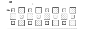
- the anti-reflection film 104 is a film that has the function of preventing diffuse reflection of radio waves between adjacent radio wave reflection devices 110 and eliminating the influence on reflected waves, and is a film that has the function of preventing radio waves from being diffusely reflected between adjacent radio wave reflection devices 110 and eliminating the influence on reflected waves. configured to absorb.
- the antireflection film 104 is provided on the adjustment substrate 106 and covers the ends of each radio wave reflection device 110. In each radio wave reflecting device 110, the peripheral end portion is covered with the anti-reflection film 104, and the portion surrounded by the anti-reflection film 104 is exposed from the anti-reflection film 104. Further, an antireflection film 104 is provided so as to overlap the area between adjacent radio wave reflection devices 110. Therefore, the antireflection film 104 has a lattice shape as a whole.
- the antireflection film 104 for example, a radio wave absorbing film that absorbs radio waves and converts them into thermal energy can be used.
- examples include resin films in which metal powder, magnetic powder such as ferrite, carbon black powder, etc. are dispersed.
- the antireflection film 104 may be formed as a continuous film having a plurality of openings that cover each end of the plurality of radio wave reflection devices 110 and overlap with a portion other than the end of each radio wave reflection device 110. good.
- the radio wave absorbing film may be formed, for example, by applying a paint containing the above powder.
- the antireflection film 104 may be composed of a plurality of arranged conductive films.
- the antireflection film 104 may be formed by arranging a plurality of conductive films 104a having a square or substantially square planar shape in an island shape. In this case, in each frame 104b forming a lattice shape (see FIG.
- the plurality of conductive films 104a can be arranged to form a plurality of rows parallel to the extending direction of the frame 104b.
- the thickness of each conductive film 104a may be determined as appropriate, and may be selected from a range of 10 nm or more and 500 nm or less, for example.
- the pitch of the conductive film 104a may be appropriately determined depending on the wavelength of the incident radio wave, and may be selected from a range of, for example, 100 ⁇ m or more and 500 ⁇ m or less.
- the conductive film 104a may be formed using a dry film forming method such as a sputtering method, a vapor deposition method, or a CVD method, or may be formed using a printing method, an inkjet method, or the like.
- each conductive film 104a may have a rectangular shape, for example, as shown in FIGS. 9A and 9B.
- the longitudinal direction of each conductive film 104a may be parallel (FIG. 9A) or perpendicular (FIG. 9B) to the direction in which the frame 104b extends (the direction indicated by the arrow in the figure). may be inclined with respect to the direction in which it is stretched.
- the plurality of conductive films 104a may form a plurality of rows in the direction in which the frame 104b extends, or as shown in FIG. 9B, a single row may be formed. . In the former case, the plurality of conductive films 104a may be arranged in a staggered manner.
- the shapes or sizes of the plurality of conductive films 104a may be the same, but as shown in FIG. 9C, the antireflection film 104 may be composed of a plurality of conductive films 104a of different shapes or sizes. In other words, two conductive films 104a selected from the plurality of conductive films 104a may have different shapes or sizes.
- each conductive film 104a may have an opening 104c.
- the shape of the opening 104c may be similar to or different from the outer contour of the conductive film 104a. Further, the shape of the opening 104c may be a polygon, or may have a shape including a curved line such as a circle or an ellipse in its outline.
- the conductive film 104a may have a circular shape, or, although not shown, may have a shape including a curved line such as an ellipse in its outline.
- the radio waves incident on the antireflection film 104 are reflected between the plurality of conductive films 104a and within the opening 104c, interfere with each other, and are attenuated. do. As a result, the radio waves are absorbed by the antireflection film 104.
- the antireflection film 104 By providing the antireflection film 104 in this manner, radio wave reflection between adjacent radio wave reflection devices 110 can be suppressed.
- FIG. 12A which is an enlarged view of FIG. 11, and a schematic diagram of the end surface along the chain line BB' in FIG.
- a plurality of protrusions 104d called structures may be formed.
- the height, width, and pitch of the projections 104d may be appropriately selected depending on the wavelength of the radio waves incident on the radio wave reflecting plate 100.
- the radio waves incident on the antireflection film 104 are repeatedly reflected on the surface of the protrusion 104d having a moth-eye structure, and the reflected radio waves and the incident radio waves interfere with each other and are attenuated. As a result, radio wave reflection between adjacent radio wave reflection devices 110 can be suppressed.
- the liquid crystal molecules are splay-aligned as described above (FIG. 13A).
- a potential difference is applied between the first electrode 132 and the second electrode 134, the liquid crystal molecules rise (FIG. 13B).
- a reflected wave (see the dotted arrow) generated by reflecting off the surface of the first electrode 132 in response to the incident radio wave (see the solid arrow in FIG. 13B) .) phase shift changes.
- the traveling direction of the radio waves changes.
- the radio wave reflecting device 110 functions as a radio wave reflecting plate that can reflect radio waves in any direction.
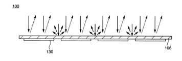
- the radio wave reflecting plate 100 since the radio wave reflecting plate 100 according to the embodiment of the present invention includes a plurality of radio wave reflecting devices 110, it can be used as a large-sized radio wave reflecting plate. However, since there is no radio wave reflecting element 130 between adjacent radio wave reflecting devices 110, radio waves cannot be reflected in a desired direction. Furthermore, since there are parts such as the connector 116 as well as the side surfaces of the first board 120 and the second board 112 between adjacent radio wave reflecting devices 110, radio waves may be reflected in a complicated manner, resulting in unintended reflections. Radio waves are diffusely reflected in the direction (see the diagonal solid line arrow in FIG. 14A). Such phenomena can cause radio interference.
- the anti-reflection film 104 is provided on the adjacent radio wave reflecting devices 110, and the radio waves incident between the adjacent radio wave reflecting devices 110 are absorbed.
- the radio waves incident between the adjacent radio wave reflecting devices 110 are absorbed.
- adjacent radio waves By significantly reducing the intensity of radio waves diffusely reflected between the reflecting devices 110, the cause of radio wave interference can be eliminated.
- radio wave reflecting element 130 included in the plurality of radio wave reflecting devices 110 that constitute the radio wave reflecting plate 100 is not limited to the above-mentioned configuration.
- the radio wave reflecting device 110 may be configured such that the second electrode 134 is not controlled for each row or column, but is controlled independently between each radio wave reflecting element 130.
- the radio wave reflecting device 110 may be configured such that the second electrode 134 is not controlled for each row or column, but is controlled independently between each radio wave reflecting element 130.
- a plurality of gate wirings extend from the gate line drive circuit 124 in the row direction.
- the gate line drive circuit 124 generates a gate signal based on a signal applied from the drive circuit on the printed circuit board 118 via the connector 116, and supplies it to a plurality of radio wave reflecting elements 130 connected to each gate line.
- signal lines (not shown) extend from the signal line drive circuit 126 in the column direction.
- the signal line drive circuit 126 generates and supplies control potentials to the plurality of radio wave reflecting elements 130 connected to each signal line based on signals supplied from the drive circuit on the printed circuit board 118.
- the gate line drive circuit 124 and the signal line drive circuit 126 may be formed of a metal film, an insulating film, or a semiconductor film provided on the second substrate 112 side of the first substrate 120, or may be formed on a semiconductor substrate.
- It may also be formed by installing an IC chip having an integrated circuit on the second substrate 112 side of the first substrate 120. Further, there is no restriction on the number of gate line drive circuits 124, and for example, a pair of gate line drive circuits 124 may be provided so as to sandwich the reflective surface.
- FIG. 16 shows a schematic top view of two adjacent radio wave reflecting elements 130
- FIG. 17 shows a schematic diagram of an end face taken along the chain line CC' in FIG.
- a transistor 148 is provided on the first substrate 120 side of the second substrate 112 directly or with a protective film 144 interposed therebetween.
- the transistor 148 illustrated in FIG. 17 is a so-called bottom-gate transistor, and includes a gate electrode 164, a gate insulating film 162 that covers the gate electrode 164, a semiconductor film 160 that overlaps with the gate electrode 164 via the gate insulating film 162, and a semiconductor film. It has a first terminal 156 and a second terminal 158 that are electrically connected to the terminal 160 .
- the transistor 148 may be a top-gate transistor or a dual-gate transistor having gate electrodes 164 above and below the semiconductor film 160, respectively. Furthermore, there are no restrictions on the upper limit relationships between the first terminal 156 and the semiconductor film 160 and between the second terminal 158 and the semiconductor film 160.
- the semiconductor film 160 may include a Group 14 element such as silicon, or may be an oxide semiconductor such as indium-gallium oxide or indium-gallium-zinc oxide.
- a first interlayer insulating film 154 made of one or more films containing silicon oxide or silicon nitride is provided so as to overlap the first terminal 156 and the second terminal 158.
- a conductive connection pad 150 is electrically connected to a second terminal 158 through an opening provided in the opening.
- a flattening film 146 for absorbing irregularities caused by the transistor 148 and the like to provide a flat surface is provided to cover the connection pad 150 directly or via a second interlayer insulating film 152.
- An opening exposing the connection pad 150 is provided in the planarization film 146 and the second interlayer insulating film 152, and the second electrode 134 located under the planarization film 146 is electrically connected to the connection pad 150 through this opening. connected.
- each radio wave reflecting element 130 may be provided with one or more transistors in addition to the transistor 148, and may also be provided with a capacitive element.
- the transistor 148 is formed on the surface of the second substrate 112 on the first substrate 120 side, and the liquid crystal layer 140 located on the first substrate 120 side of the transistor 148 is controlled.
- an element such as the transistor 148 may be formed on the surface of the first substrate 120 on the second substrate 112 side, and the liquid crystal layer 140 located thereon may be controlled.
- On/off of the transistor 148 is controlled by a signal supplied via the gate wiring.
- the control potential supplied via the signal line is applied to the second electrode 134 via the transistor 148. Therefore, a control potential can be individually supplied to each radio wave reflecting element 130.
- the first electrode 132 is supplied with a potential commonly given to the plurality of radio wave reflecting elements 130 (common potential). An electric field is generated between the first electrode 132 and the second electrode 134 due to the difference between the common potential and the control potential, and the dielectric constant of the liquid crystal layer 140 is controlled for each radio wave reflecting element 130.
- Radio wave reflection plate 102: Housing, 104: Anti-reflection film, 104a: Conductive film, 104b: Frame, 104c: Opening, 104d: Projection, 106: Adjustment substrate, 108: Adhesive layer, 110: Radio wave reflection device , 112: second substrate, 114: terminal, 116: connector, 118: printed circuit board, 120: first substrate, 122: sealing material, 124: gate line drive circuit, 126: signal line drive circuit, 130: Radio wave reflecting element, 132: first electrode, 134: second electrode, 136: protective film, 138: first alignment film, 140: liquid crystal layer, 142: second alignment film, 144: protective film, 146 : Planarization film, 148: Transistor, 150: Connection pad, 152: Second interlayer insulating film, 154: First interlayer insulating film, 156: First terminal, 158: Second terminal, 160: Semiconductor film , 162: Gate insulating film, 164: Gate electrode
Landscapes
- Physics & Mathematics (AREA)
- Electromagnetism (AREA)
- Aerials With Secondary Devices (AREA)
Priority Applications (4)
| Application Number | Priority Date | Filing Date | Title |
|---|---|---|---|
| DE112023000432.3T DE112023000432T5 (de) | 2022-03-17 | 2023-03-02 | Radiowellen reflektierendes Panel |
| JP2024507720A JPWO2023176472A1 (https=) | 2022-03-17 | 2023-03-02 | |
| CN202380024590.9A CN118786581A (zh) | 2022-03-17 | 2023-03-02 | 电波反射板 |
| US18/804,145 US12586922B2 (en) | 2022-03-17 | 2024-08-14 | Intelligent reflecting surface |
Applications Claiming Priority (2)
| Application Number | Priority Date | Filing Date | Title |
|---|---|---|---|
| JP2022042989 | 2022-03-17 | ||
| JP2022-042989 | 2022-03-17 |
Related Child Applications (1)
| Application Number | Title | Priority Date | Filing Date |
|---|---|---|---|
| US18/804,145 Continuation US12586922B2 (en) | 2022-03-17 | 2024-08-14 | Intelligent reflecting surface |
Publications (1)
| Publication Number | Publication Date |
|---|---|
| WO2023176472A1 true WO2023176472A1 (ja) | 2023-09-21 |
Family
ID=88023629
Family Applications (1)
| Application Number | Title | Priority Date | Filing Date |
|---|---|---|---|
| PCT/JP2023/007788 Ceased WO2023176472A1 (ja) | 2022-03-17 | 2023-03-02 | 電波反射板 |
Country Status (5)
| Country | Link |
|---|---|
| US (1) | US12586922B2 (https=) |
| JP (1) | JPWO2023176472A1 (https=) |
| CN (1) | CN118786581A (https=) |
| DE (1) | DE112023000432T5 (https=) |
| WO (1) | WO2023176472A1 (https=) |
Cited By (2)
| Publication number | Priority date | Publication date | Assignee | Title |
|---|---|---|---|---|
| WO2025169782A1 (ja) * | 2024-02-06 | 2025-08-14 | 株式会社ジャパンディスプレイ | 電波反射装置の調整方法 |
| WO2025169809A1 (ja) * | 2024-02-06 | 2025-08-14 | 株式会社ジャパンディスプレイ | 電波反射装置 |
Citations (4)
| Publication number | Priority date | Publication date | Assignee | Title |
|---|---|---|---|---|
| JP2019530387A (ja) * | 2016-09-22 | 2019-10-17 | 華為技術有限公司Huawei Technologies Co.,Ltd. | ビーム・ステアリング・アンテナのための液晶調整可能メタサーフェス |
| JP2021175054A (ja) * | 2020-04-22 | 2021-11-01 | Kddi株式会社 | メタサーフェス反射板アレイ |
| WO2022244676A1 (ja) * | 2021-05-17 | 2022-11-24 | 株式会社ジャパンディスプレイ | 電波反射板および電波反射装置 |
| WO2022259790A1 (ja) * | 2021-06-09 | 2022-12-15 | 株式会社ジャパンディスプレイ | 電波反射板 |
Family Cites Families (3)
| Publication number | Priority date | Publication date | Assignee | Title |
|---|---|---|---|---|
| JPH11103201A (ja) | 1997-09-29 | 1999-04-13 | Mitsui Chem Inc | 移相器、移相器アレイおよびフェーズドアレイアンテナ装置 |
| KR20150137148A (ko) * | 2014-05-28 | 2015-12-09 | 삼성디스플레이 주식회사 | 액정 표시 장치 및 이의 제조 방법 |
| CN118285023A (zh) * | 2021-11-25 | 2024-07-02 | 株式会社日本显示器 | 电波反射板 |
-
2023
- 2023-03-02 JP JP2024507720A patent/JPWO2023176472A1/ja active Pending
- 2023-03-02 WO PCT/JP2023/007788 patent/WO2023176472A1/ja not_active Ceased
- 2023-03-02 CN CN202380024590.9A patent/CN118786581A/zh active Pending
- 2023-03-02 DE DE112023000432.3T patent/DE112023000432T5/de active Pending
-
2024
- 2024-08-14 US US18/804,145 patent/US12586922B2/en active Active
Patent Citations (4)
| Publication number | Priority date | Publication date | Assignee | Title |
|---|---|---|---|---|
| JP2019530387A (ja) * | 2016-09-22 | 2019-10-17 | 華為技術有限公司Huawei Technologies Co.,Ltd. | ビーム・ステアリング・アンテナのための液晶調整可能メタサーフェス |
| JP2021175054A (ja) * | 2020-04-22 | 2021-11-01 | Kddi株式会社 | メタサーフェス反射板アレイ |
| WO2022244676A1 (ja) * | 2021-05-17 | 2022-11-24 | 株式会社ジャパンディスプレイ | 電波反射板および電波反射装置 |
| WO2022259790A1 (ja) * | 2021-06-09 | 2022-12-15 | 株式会社ジャパンディスプレイ | 電波反射板 |
Cited By (2)
| Publication number | Priority date | Publication date | Assignee | Title |
|---|---|---|---|---|
| WO2025169782A1 (ja) * | 2024-02-06 | 2025-08-14 | 株式会社ジャパンディスプレイ | 電波反射装置の調整方法 |
| WO2025169809A1 (ja) * | 2024-02-06 | 2025-08-14 | 株式会社ジャパンディスプレイ | 電波反射装置 |
Also Published As
| Publication number | Publication date |
|---|---|
| US12586922B2 (en) | 2026-03-24 |
| JPWO2023176472A1 (https=) | 2023-09-21 |
| CN118786581A (zh) | 2024-10-15 |
| DE112023000432T5 (de) | 2024-09-26 |
| US20240405441A1 (en) | 2024-12-05 |
Similar Documents
| Publication | Publication Date | Title |
|---|---|---|
| US12586922B2 (en) | Intelligent reflecting surface | |
| JP7367160B2 (ja) | 表示装置 | |
| TWI553381B (zh) | 顯示面板 | |
| JP7849054B2 (ja) | 電波反射素子および電波反射板 | |
| US11686975B2 (en) | Imaging device having dimming element | |
| US20100141859A1 (en) | Display device including uv-absorbing filter | |
| JP5571641B2 (ja) | 液晶表示装置 | |
| WO2023058399A1 (ja) | 電波反射装置 | |
| US20250372884A1 (en) | Reflecting device | |
| US9971192B2 (en) | Display panel and display device having the same | |
| TWI242091B (en) | Liquid crystal display cell and liquid crystal display | |
| CN112612373B (zh) | 一种显示面板和显示装置 | |
| US11340493B2 (en) | Display device | |
| US12169340B2 (en) | Electronic device with a transparent electrode and a signal line electrically connected thereto | |
| WO2025169809A1 (ja) | 電波反射装置 | |
| WO2025220602A1 (ja) | 電波反射装置 | |
| WO2026070039A1 (ja) | 電波反射装置 | |
| CN114551478A (zh) | 显示面板及移动终端 | |
| WO2024209885A1 (ja) | 電波反射装置 | |
| CN113176683A (zh) | 显示装置 | |
| WO2025033055A1 (ja) | 電波反射装置 | |
| CN113093422B (zh) | 显示面板及显示面板的制备方法 | |
| WO2026053687A1 (ja) | フェーズドアレイアンテナ | |
| WO2024176879A1 (ja) | 電波反射板及び電波反射装置 | |
| KR20070028044A (ko) | 액정 표시 장치 |
Legal Events
| Date | Code | Title | Description |
|---|---|---|---|
| 121 | Ep: the epo has been informed by wipo that ep was designated in this application |
Ref document number: 23770430 Country of ref document: EP Kind code of ref document: A1 |
|
| WWE | Wipo information: entry into national phase |
Ref document number: 202380024590.9 Country of ref document: CN |
|
| ENP | Entry into the national phase |
Ref document number: 2024507720 Country of ref document: JP Kind code of ref document: A |
|
| 122 | Ep: pct application non-entry in european phase |
Ref document number: 23770430 Country of ref document: EP Kind code of ref document: A1 |