WO2023157819A1 - Dispositif de photodétection et instrument électronique - Google Patents
Dispositif de photodétection et instrument électronique Download PDFInfo
- Publication number
- WO2023157819A1 WO2023157819A1 PCT/JP2023/004902 JP2023004902W WO2023157819A1 WO 2023157819 A1 WO2023157819 A1 WO 2023157819A1 JP 2023004902 W JP2023004902 W JP 2023004902W WO 2023157819 A1 WO2023157819 A1 WO 2023157819A1
- Authority
- WO
- WIPO (PCT)
- Prior art keywords
- transistor
- pixel
- region
- semiconductor region
- semiconductor
- Prior art date
Links
- 239000004065 semiconductor Substances 0.000 claims abstract description 408
- 238000006243 chemical reaction Methods 0.000 claims abstract description 120
- 238000009792 diffusion process Methods 0.000 claims description 74
- 238000007667 floating Methods 0.000 claims description 71
- 239000004020 conductor Substances 0.000 claims description 54
- 230000003321 amplification Effects 0.000 claims description 50
- 238000003199 nucleic acid amplification method Methods 0.000 claims description 50
- 238000002955 isolation Methods 0.000 claims description 35
- 230000003287 optical effect Effects 0.000 claims description 29
- 239000012535 impurity Substances 0.000 claims description 21
- 238000000926 separation method Methods 0.000 claims description 16
- 230000000903 blocking effect Effects 0.000 claims description 3
- 238000003384 imaging method Methods 0.000 description 243
- 239000010410 layer Substances 0.000 description 129
- 238000010586 diagram Methods 0.000 description 98
- 238000012986 modification Methods 0.000 description 70
- 230000004048 modification Effects 0.000 description 70
- 238000012545 processing Methods 0.000 description 48
- 238000012546 transfer Methods 0.000 description 39
- 210000003128 head Anatomy 0.000 description 26
- 238000001514 detection method Methods 0.000 description 25
- 238000004891 communication Methods 0.000 description 18
- 230000001276 controlling effect Effects 0.000 description 17
- 238000005516 engineering process Methods 0.000 description 16
- 239000000758 substrate Substances 0.000 description 15
- 230000000875 corresponding effect Effects 0.000 description 12
- 229910021420 polycrystalline silicon Inorganic materials 0.000 description 11
- 229920005591 polysilicon Polymers 0.000 description 11
- 238000002674 endoscopic surgery Methods 0.000 description 10
- 230000006870 function Effects 0.000 description 10
- 230000006866 deterioration Effects 0.000 description 9
- 101710170230 Antimicrobial peptide 1 Proteins 0.000 description 8
- 101710170231 Antimicrobial peptide 2 Proteins 0.000 description 7
- 239000007769 metal material Substances 0.000 description 7
- 229910052581 Si3N4 Inorganic materials 0.000 description 6
- 230000005540 biological transmission Effects 0.000 description 6
- 230000008859 change Effects 0.000 description 6
- 239000010949 copper Substances 0.000 description 6
- HQVNEWCFYHHQES-UHFFFAOYSA-N silicon nitride Chemical compound N12[Si]34N5[Si]62N3[Si]51N64 HQVNEWCFYHHQES-UHFFFAOYSA-N 0.000 description 6
- XUIMIQQOPSSXEZ-UHFFFAOYSA-N Silicon Chemical compound [Si] XUIMIQQOPSSXEZ-UHFFFAOYSA-N 0.000 description 5
- 238000000034 method Methods 0.000 description 5
- 229910052710 silicon Inorganic materials 0.000 description 5
- 239000010703 silicon Substances 0.000 description 5
- 238000001356 surgical procedure Methods 0.000 description 5
- WFKWXMTUELFFGS-UHFFFAOYSA-N tungsten Chemical compound [W] WFKWXMTUELFFGS-UHFFFAOYSA-N 0.000 description 5
- 229910052721 tungsten Inorganic materials 0.000 description 5
- 239000010937 tungsten Substances 0.000 description 5
- 229910052782 aluminium Inorganic materials 0.000 description 4
- XAGFODPZIPBFFR-UHFFFAOYSA-N aluminium Chemical compound [Al] XAGFODPZIPBFFR-UHFFFAOYSA-N 0.000 description 4
- 230000005684 electric field Effects 0.000 description 4
- 230000005284 excitation Effects 0.000 description 4
- 239000000463 material Substances 0.000 description 4
- 230000007246 mechanism Effects 0.000 description 4
- 101100191136 Arabidopsis thaliana PCMP-A2 gene Proteins 0.000 description 3
- RYGMFSIKBFXOCR-UHFFFAOYSA-N Copper Chemical compound [Cu] RYGMFSIKBFXOCR-UHFFFAOYSA-N 0.000 description 3
- 208000005646 Pneumoperitoneum Diseases 0.000 description 3
- 101100422768 Saccharomyces cerevisiae (strain ATCC 204508 / S288c) SUL2 gene Proteins 0.000 description 3
- 101100048260 Saccharomyces cerevisiae (strain ATCC 204508 / S288c) UBX2 gene Proteins 0.000 description 3
- VYPSYNLAJGMNEJ-UHFFFAOYSA-N Silicium dioxide Chemical compound O=[Si]=O VYPSYNLAJGMNEJ-UHFFFAOYSA-N 0.000 description 3
- 229910052802 copper Inorganic materials 0.000 description 3
- 238000013461 design Methods 0.000 description 3
- 230000000694 effects Effects 0.000 description 3
- 238000010336 energy treatment Methods 0.000 description 3
- 239000011810 insulating material Substances 0.000 description 3
- 239000011229 interlayer Substances 0.000 description 3
- 238000005259 measurement Methods 0.000 description 3
- 150000004767 nitrides Chemical class 0.000 description 3
- LIVNPJMFVYWSIS-UHFFFAOYSA-N silicon monoxide Chemical compound [Si-]#[O+] LIVNPJMFVYWSIS-UHFFFAOYSA-N 0.000 description 3
- 229910052814 silicon oxide Inorganic materials 0.000 description 3
- HODRFAVLXIFVTR-RKDXNWHRSA-N tevenel Chemical compound NS(=O)(=O)C1=CC=C([C@@H](O)[C@@H](CO)NC(=O)C(Cl)Cl)C=C1 HODRFAVLXIFVTR-RKDXNWHRSA-N 0.000 description 3
- 101100205847 Mus musculus Srst gene Proteins 0.000 description 2
- 229910000577 Silicon-germanium Inorganic materials 0.000 description 2
- 230000009471 action Effects 0.000 description 2
- 210000004204 blood vessel Anatomy 0.000 description 2
- 239000003153 chemical reaction reagent Substances 0.000 description 2
- 230000000295 complement effect Effects 0.000 description 2
- 239000000470 constituent Substances 0.000 description 2
- 238000005401 electroluminescence Methods 0.000 description 2
- 229910000449 hafnium oxide Inorganic materials 0.000 description 2
- MOFVSTNWEDAEEK-UHFFFAOYSA-M indocyanine green Chemical compound [Na+].[O-]S(=O)(=O)CCCCN1C2=CC=C3C=CC=CC3=C2C(C)(C)C1=CC=CC=CC=CC1=[N+](CCCCS([O-])(=O)=O)C2=CC=C(C=CC=C3)C3=C2C1(C)C MOFVSTNWEDAEEK-UHFFFAOYSA-M 0.000 description 2
- 229960004657 indocyanine green Drugs 0.000 description 2
- 238000009434 installation Methods 0.000 description 2
- 239000012212 insulator Substances 0.000 description 2
- 230000001678 irradiating effect Effects 0.000 description 2
- 229910044991 metal oxide Inorganic materials 0.000 description 2
- 150000004706 metal oxides Chemical class 0.000 description 2
- 230000003071 parasitic effect Effects 0.000 description 2
- 230000002194 synthesizing effect Effects 0.000 description 2
- 240000004050 Pentaglottis sempervirens Species 0.000 description 1
- 235000004522 Pentaglottis sempervirens Nutrition 0.000 description 1
- 101100386054 Saccharomyces cerevisiae (strain ATCC 204508 / S288c) CYS3 gene Proteins 0.000 description 1
- NRTOMJZYCJJWKI-UHFFFAOYSA-N Titanium nitride Chemical compound [Ti]#N NRTOMJZYCJJWKI-UHFFFAOYSA-N 0.000 description 1
- LEVVHYCKPQWKOP-UHFFFAOYSA-N [Si].[Ge] Chemical compound [Si].[Ge] LEVVHYCKPQWKOP-UHFFFAOYSA-N 0.000 description 1
- 230000001133 acceleration Effects 0.000 description 1
- 238000009825 accumulation Methods 0.000 description 1
- 230000002411 adverse Effects 0.000 description 1
- 230000015572 biosynthetic process Effects 0.000 description 1
- 230000000740 bleeding effect Effects 0.000 description 1
- 239000000872 buffer Substances 0.000 description 1
- 238000002485 combustion reaction Methods 0.000 description 1
- 239000002131 composite material Substances 0.000 description 1
- 150000001875 compounds Chemical class 0.000 description 1
- 238000012937 correction Methods 0.000 description 1
- 230000002596 correlated effect Effects 0.000 description 1
- 230000007547 defect Effects 0.000 description 1
- 238000011161 development Methods 0.000 description 1
- 238000002073 fluorescence micrograph Methods 0.000 description 1
- 229910052735 hafnium Inorganic materials 0.000 description 1
- VBJZVLUMGGDVMO-UHFFFAOYSA-N hafnium atom Chemical compound [Hf] VBJZVLUMGGDVMO-UHFFFAOYSA-N 0.000 description 1
- WIHZLLGSGQNAGK-UHFFFAOYSA-N hafnium(4+);oxygen(2-) Chemical compound [O-2].[O-2].[Hf+4] WIHZLLGSGQNAGK-UHFFFAOYSA-N 0.000 description 1
- 229910000765 intermetallic Inorganic materials 0.000 description 1
- 238000005468 ion implantation Methods 0.000 description 1
- 238000010030 laminating Methods 0.000 description 1
- 230000031700 light absorption Effects 0.000 description 1
- 239000004973 liquid crystal related substance Substances 0.000 description 1
- 238000012423 maintenance Methods 0.000 description 1
- 239000011159 matrix material Substances 0.000 description 1
- 229910052751 metal Inorganic materials 0.000 description 1
- 239000002184 metal Substances 0.000 description 1
- 150000002736 metal compounds Chemical class 0.000 description 1
- 239000003595 mist Substances 0.000 description 1
- 230000000116 mitigating effect Effects 0.000 description 1
- 239000000203 mixture Substances 0.000 description 1
- 239000013307 optical fiber Substances 0.000 description 1
- 230000001151 other effect Effects 0.000 description 1
- 230000002093 peripheral effect Effects 0.000 description 1
- 238000007639 printing Methods 0.000 description 1
- 230000008569 process Effects 0.000 description 1
- 210000001747 pupil Anatomy 0.000 description 1
- 230000009467 reduction Effects 0.000 description 1
- 238000005070 sampling Methods 0.000 description 1
- 238000007789 sealing Methods 0.000 description 1
- 230000035939 shock Effects 0.000 description 1
- 239000002356 single layer Substances 0.000 description 1
- 101150035983 str1 gene Proteins 0.000 description 1
- 239000002344 surface layer Substances 0.000 description 1
- MZLGASXMSKOWSE-UHFFFAOYSA-N tantalum nitride Chemical compound [Ta]#N MZLGASXMSKOWSE-UHFFFAOYSA-N 0.000 description 1
- 230000000007 visual effect Effects 0.000 description 1
Images


Classifications
-
- H—ELECTRICITY
- H01—ELECTRIC ELEMENTS
- H01L—SEMICONDUCTOR DEVICES NOT COVERED BY CLASS H10
- H01L27/00—Devices consisting of a plurality of semiconductor or other solid-state components formed in or on a common substrate
- H01L27/14—Devices consisting of a plurality of semiconductor or other solid-state components formed in or on a common substrate including semiconductor components sensitive to infrared radiation, light, electromagnetic radiation of shorter wavelength or corpuscular radiation and specially adapted either for the conversion of the energy of such radiation into electrical energy or for the control of electrical energy by such radiation
- H01L27/144—Devices controlled by radiation
- H01L27/146—Imager structures
Definitions
- the present disclosure relates to photodetection devices and electronic devices.
- a device has been proposed that has a GND (ground) contact for each pixel and photoelectrically converts incident light (Patent Document 1).
- a photodetector includes a semiconductor layer, a plurality of pixels including a first pixel having a photoelectric conversion element provided in the semiconductor layer, and a plurality of adjacent pixels provided in the semiconductor layer. a trench;
- the first pixel includes a transistor provided on the first surface side of the semiconductor layer, a first conductivity type first semiconductor region provided on the first surface side of the semiconductor layer, and electrically connected to the first semiconductor region. and a first contact.
- the first semiconductor region is in contact with the transistor.
- a photodetector includes a first pixel provided in a semiconductor layer, a first region separating the first pixel from a pixel adjacent to the first pixel, and a photoelectric conversion element provided in the first pixel.
- the second region has a first separating portion between the first floating diffusion region and the second floating diffusion region provided in the first pixel in plan view.
- the second region has a second isolation portion between the first transistor and the second transistor provided in the first pixel in plan view.
- the first pixel includes a first conductivity type first semiconductor region and a first contact electrically connected to the first semiconductor region.
- a first semiconductor region is provided between the first isolation portion and the second isolation portion in plan view. The first semiconductor region contacts the first transistor and the second transistor.
- An electronic device includes an optical system and a photodetector that receives light transmitted through the optical system.
- the photodetector includes a semiconductor layer, a plurality of pixels including a first pixel having a photoelectric conversion element provided in the semiconductor layer, and trenches provided between adjacent pixels in the semiconductor layer.
- the first pixel includes a transistor provided on the first surface side of the semiconductor layer, a first conductivity type first semiconductor region provided on the first surface side of the semiconductor layer, and electrically connected to the first semiconductor region. and a first contact.
- the first semiconductor region is in contact with the transistor.
- An electronic device includes an optical system and a photodetector that receives light transmitted through the optical system.
- a first pixel provided in a semiconductor layer, a first region separating the first pixel and an adjacent pixel, and a photoelectric conversion element provided in the first pixel are blocked in plan view.
- the second region has a first separating portion between the first floating diffusion region and the second floating diffusion region provided in the first pixel in plan view.
- the second region has a second isolation portion between the first transistor and the second transistor provided in the first pixel in plan view.
- the first pixel includes a first conductivity type first semiconductor region and a first contact electrically connected to the first semiconductor region.
- a first semiconductor region is provided between the first isolation portion and the second isolation portion in plan view. The first semiconductor region contacts the first transistor and the second transistor.
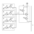
- FIG. 1 is a block diagram illustrating an example of a schematic configuration of an imaging device, which is an example of a photodetection device according to a first embodiment of the present disclosure.
- FIG. 2 is a diagram illustrating an arrangement example of pixels of the imaging device according to the first embodiment of the present disclosure.
- FIG. 3 is a diagram for explaining an example of a circuit configuration of a pixel of the imaging device according to the first embodiment of the present disclosure;
- FIG. 4A is a diagram for explaining another example of the circuit configuration of the pixels of the imaging device according to the first embodiment of the present disclosure; 4B is a diagram for explaining another example of the circuit configuration of the pixels of the imaging device according to the first embodiment of the present disclosure;
- FIG. 5 is a diagram illustrating an example of a planar configuration of pixels of the imaging device according to the first embodiment of the present disclosure
- FIG. 6 is a diagram for explaining an example of a cross-sectional configuration of a pixel of the imaging device according to the first embodiment of the present disclosure
- FIG. 7 is a diagram for explaining an example of a cross-sectional configuration of a pixel of the imaging device according to the first embodiment of the present disclosure
- FIG. 8 is a diagram illustrating an arrangement example of pixel transistors of the imaging device according to the first embodiment of the present disclosure.
- FIG. 9 is a diagram illustrating another arrangement example of pixel transistors of the imaging device according to the first embodiment of the present disclosure.
- FIG. 10 is a diagram illustrating another arrangement example of pixel transistors of the imaging device according to the first embodiment of the present disclosure.
- FIG. 11 is a diagram illustrating an example of a cross-sectional configuration of an imaging device according to the first embodiment of the present disclosure;
- FIG. 12 is a diagram illustrating an example of a planar configuration of pixels of an imaging device according to Modification 1 of the present disclosure.
- FIG. 13 is a diagram for explaining an example of a cross-sectional configuration of pixels of an imaging device according to Modification 1 of the present disclosure.
- FIG. 14 is a diagram for explaining an example of a planar configuration of an imaging device according to Modification 1 of the present disclosure.
- FIG. 11 is a diagram illustrating another arrangement example of pixel transistors of the imaging device according to the first embodiment of the present disclosure.
- FIG. 11 is a diagram illustrating an example of a cross-sectional configuration of an imaging device according to the first embodiment of the present disclosure.
- FIG. 12 is a diagram illustrating an example of
- FIG. 15 is a diagram for explaining an example of a cross-sectional configuration of an imaging device according to Modification 1 of the present disclosure.
- FIG. 16 is a diagram for explaining another example of the cross-sectional configuration of the pixels of the imaging device according to Modification 1 of the present disclosure.
- FIG. 17 is a diagram for explaining another example of the cross-sectional configuration of the pixels of the imaging device according to Modification 1 of the present disclosure.
- FIG. 18 is a diagram illustrating an example of a planar configuration of pixels of an imaging device according to Modification 2 of the present disclosure.
- FIG. 19 is a diagram for explaining an example of a planar configuration of an imaging device according to Modification 2 of the present disclosure.
- FIG. 19 is a diagram for explaining an example of a planar configuration of an imaging device according to Modification 2 of the present disclosure.
- FIG. 20 is a diagram illustrating an example of a planar configuration of pixels of an imaging device according to Modification 3 of the present disclosure.
- FIG. 21 is a diagram for explaining an example of a cross-sectional configuration of a pixel of an imaging device according to Modification 3 of the present disclosure.
- FIG. 22 is a diagram illustrating another example of a planar configuration of pixels of an imaging device according to Modification 3 of the present disclosure.
- FIG. 23 is a diagram for explaining another example of the cross-sectional configuration of the pixels of the imaging device according to Modification 3 of the present disclosure.
- FIG. 24 is a diagram for explaining another example of the cross-sectional configuration of the pixels of the imaging device according to Modification 3 of the present disclosure.
- FIG. 21 is a diagram for explaining an example of a cross-sectional configuration of a pixel of an imaging device according to Modification 3 of the present disclosure.
- FIG. 22 is a diagram illustrating another example of a planar configuration of pixels of an imaging device according to Modification 3 of the
- FIG. 25 is a diagram illustrating another example of a planar configuration of pixels of an imaging device according to Modification 3 of the present disclosure.
- FIG. 26 is a diagram for explaining another example of the cross-sectional configuration of the pixels of the imaging device according to Modification 3 of the present disclosure.
- FIG. 27 is a diagram for explaining another example of the cross-sectional configuration of the pixels of the imaging device according to Modification 3 of the present disclosure.
- FIG. 28 is a diagram for explaining an arrangement example of pixel transistors of an imaging device according to Modification 4 of the present disclosure.
- FIG. 29 is a diagram for explaining another arrangement example of the pixel transistors of the imaging device according to Modification 4 of the present disclosure.
- FIG. 30 is a diagram for explaining another arrangement example of the pixel transistors of the imaging device according to Modification 4 of the present disclosure.
- FIG. 31 is a diagram for explaining another arrangement example of the pixel transistors of the imaging device according to Modification 4 of the present disclosure.
- FIG. 32 is a diagram for explaining another arrangement example of the pixel transistors of the imaging device according to Modification 4 of the present disclosure.
- FIG. 33 is a diagram for explaining another arrangement example of the pixel transistors of the imaging device according to Modification 4 of the present disclosure.
- FIG. 34 is a diagram for explaining another arrangement example of the pixel transistors of the imaging device according to Modification 4 of the present disclosure.
- FIG. 35 is a diagram for explaining another arrangement example of the pixel transistors of the imaging device according to Modification 4 of the present disclosure.
- FIG. 31 is a diagram for explaining another arrangement example of the pixel transistors of the imaging device according to Modification 4 of the present disclosure.
- FIG. 32 is a diagram for explaining another arrangement example of the pixel
- FIG. 36 is a diagram illustrating an arrangement example of pixels of an imaging device according to the second embodiment of the present disclosure.
- 37 is a diagram illustrating an example of a planar configuration of pixels of an imaging device according to the second embodiment of the present disclosure.
- FIG. 38 is a diagram illustrating another example of a planar configuration of pixels of the imaging device according to the second embodiment of the present disclosure;
- FIG. 39 is a diagram illustrating an example of a planar configuration of pixels of an imaging device according to Modification 5 of the present disclosure.
- 40 is a diagram for explaining an example of a cross-sectional configuration of a pixel of an imaging device according to Modification 5 of the present disclosure;
- FIG. 41 is a diagram for explaining another example of the cross-sectional configuration of the pixels of the imaging device according to Modification 5 of the present disclosure.
- FIG. 42 is a diagram for explaining another example of the planar configuration of the pixels of the imaging device according to Modification 5 of the present disclosure.
- 43A is a diagram for explaining a configuration example of a pixel of an imaging device according to Modification 6 of the present disclosure;
- FIG. 43B is a diagram for explaining a configuration example of a pixel of an imaging device according to Modification 6 of the present disclosure;
- FIG. 44 is a diagram for explaining a configuration example of pixels of an imaging device according to Modification 7 of the present disclosure.
- FIG. 45 is a diagram illustrating an example of a planar configuration of pixels of an imaging device according to Modification 7 of the present disclosure.
- FIG. 46 is a diagram illustrating an example of a planar configuration of pixels of an imaging device according to Modification 8 of the present disclosure.
- FIG. 47 is a diagram illustrating another example of the planar configuration of the pixels of the imaging device according to Modification 8 of the present disclosure.
- FIG. 48 is a diagram illustrating an example of a planar configuration of pixels of an imaging device according to Modification 9 of the present disclosure.
- 49 is a diagram for explaining an example of a cross-sectional configuration of a pixel of an imaging device according to Modification 9 of the present disclosure; FIG. FIG.
- FIG. 50 is a diagram for explaining another example of the planar configuration of the pixels of the imaging device according to Modification 9 of the present disclosure.
- FIG. 51 is a diagram illustrating an example of a planar configuration of pixels of an imaging device according to Modification 10 of the present disclosure.
- FIG. 52 is a diagram illustrating another example of the planar configuration of the pixels of the imaging device according to Modification 10 of the present disclosure.
- FIG. 53 is a diagram illustrating another example of the planar configuration of the pixels of the imaging device according to Modification 10 of the present disclosure.
- FIG. 54 is a block diagram showing a configuration example of an electronic device having an imaging device.
- FIG. 55 is a block diagram showing an example of a schematic configuration of a vehicle control system.
- FIG. 51 is a diagram illustrating an example of a planar configuration of pixels of an imaging device according to Modification 10 of the present disclosure.
- FIG. 52 is a diagram illustrating another example of the planar configuration of the pixels of the imaging device according to Modification 10 of the
- FIG. 56 is an explanatory diagram showing an example of installation positions of the vehicle exterior information detection unit and the imaging unit.
- FIG. 57 is a diagram showing an example of a schematic configuration of an endoscopic surgery system.
- FIG. 58 is a block diagram showing an example of the functional configuration of the camera head and CCU.
- FIG. 1 is a block diagram illustrating an example of a schematic configuration of an imaging device, which is an example of a photodetection device according to a first embodiment of the present disclosure.
- a photodetector is a device capable of detecting incident light.
- the imaging device 1, which is a photodetector has a plurality of pixels P each having a photoelectric conversion unit (photoelectric conversion element), and is configured to photoelectrically convert incident light to generate a signal.
- the imaging device 1 (photodetector) can generate a signal by receiving light that has passed through an optical system (not shown) including an optical lens.
- the imaging device 1 is configured using, for example, a semiconductor substrate (for example, a silicon substrate) on which a plurality of pixels P are provided.
- a photoelectric conversion unit of each pixel P of the imaging device 1 is, for example, a photodiode (PD), and is configured to be capable of photoelectrically converting light.
- the imaging device 1 has an area (pixel section 100) in which a plurality of pixels P are two-dimensionally arranged in a matrix as an imaging area.
- the pixel section 100 can also be said to be a pixel array in which a plurality of pixels P are arranged.
- the imaging device 1 captures incident light (image light) from a subject through an optical system including an optical lens.
- the imaging device 1 captures an image of a subject formed by an optical lens.
- the imaging device 1 can photoelectrically convert the received light to generate a pixel signal.
- the imaging device 1 is, for example, a CMOS (Complementary Metal Oxide Semiconductor) image sensor.
- the imaging device 1 can be used in electronic devices such as digital still cameras, video cameras, and mobile phones.
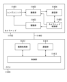
- the imaging device 1 has, for example, a pixel driving section 111, a signal processing section 112, a control section 113, a processing section 114, etc. in the peripheral area of the pixel section 100 (pixel array). Further, the imaging device 1 is provided with a plurality of control lines L1 and a plurality of signal lines L2.
- the control line L1 is a signal line capable of transmitting a signal for controlling the pixel P, and is connected to the pixel driving section 111 and the pixel P of the pixel section 100.
- a plurality of control lines L1 are wired for each pixel row composed of a plurality of pixels P arranged in the horizontal direction (row direction).
- the control line L1 is configured to transmit a control signal for signal readout from the pixel P.
- the plurality of control lines L1 for each pixel row of the imaging device 1 include, for example, wiring for transmitting signals for controlling transfer transistors, wiring for transmitting signals for controlling select transistors, and wiring for transmitting signals for controlling reset transistors. Wiring etc. are included.
- the control line L1 can also be said to be a drive line (pixel drive line) that transmits a signal for driving the pixels P. FIG.
- a signal line L2 is a signal line capable of transmitting a signal from the pixel P, and is connected to the pixel P of the pixel section 100 and the signal processing section 112.
- a signal line L2 is wired for each pixel column composed of a plurality of pixels P arranged in the vertical direction (column direction).
- the signal line L2 is a vertical signal line and is configured to transmit signals output from the pixels P. As shown in FIG.
- the pixel driving section 111 is configured to be able to drive each pixel P of the pixel section 100 .
- the pixel driving unit 111 is a driving circuit, and is composed of a plurality of circuits including, for example, buffers, shift registers, address decoders, and the like.
- the pixel driving section 111 generates a signal for driving the pixel P and outputs it to each pixel P of the pixel section 100 via the control line L1.
- the pixel drive unit 111 is controlled by the control unit 113 and controls the pixels P of the pixel unit 100 .
- the pixel drive unit 111 generates signals for controlling the pixels P such as, for example, signals for controlling the transfer transistors of the pixels P, signals for controlling the selection transistors, and signals for controlling the reset transistors. supplied to each pixel P.
- the pixel drive unit 111 can control reading out pixel signals from each pixel P.
- FIG. The pixel drive section 111 can also be said to be a pixel control section configured to be able to control each pixel P.
- FIG. Note that the pixel driving unit 111 and the control unit 113 can be collectively referred to as a pixel control unit.
- the signal processing unit 112 is configured to be able to execute signal processing of input pixel signals.
- the signal processing unit 112 is a signal processing circuit, and has, for example, a load circuit unit, an AD (Analog Digital) conversion unit, a horizontal selection switch, and the like. Note that the signal processing unit 112 may have an amplifier circuit unit configured to amplify the signal read out from the pixel P via the signal line L2.
- a signal output from each pixel P selectively scanned by the pixel drive unit 111 is input to the signal processing unit 112 via the signal line L2.
- the signal processing unit 112 can perform signal processing such as AD conversion of the signal of the pixel P and CDS (Correlated Double Sampling).
- a signal of each pixel P transmitted through each of the signal lines L2 is subjected to signal processing by the signal processing unit 112 and output to the processing unit 114 .
- the processing unit 114 is configured to be able to perform signal processing on the input signal.
- the processing unit 114 is a signal processing circuit, and is configured by, for example, a circuit that performs various types of signal processing on pixel signals.
- Processing unit 114 may include a processor and memory.
- the processing unit 114 performs signal processing on the pixel signals input from the signal processing unit 112 and outputs the processed pixel signals.
- the processing unit 114 can perform various kinds of signal processing such as noise reduction processing and gradation correction processing, for example.
- the control unit 113 is configured to be able to control each unit of the imaging device 1 .
- the control unit 113 can receive a clock given from the outside, data instructing an operation mode, and the like, and can output data such as internal information of the imaging device 1 .
- the control unit 113 is a control circuit, and has, for example, a timing generator configured to generate various timing signals.
- the control unit 113 controls driving of the pixel driving unit 111, the signal processing unit 112, etc., based on various timing signals (pulse signals, clock signals, etc.) generated by the timing generator. Note that the control unit 113 and the processing unit 114 may be configured integrally.
- the pixel driving unit 111, the signal processing unit 112, the control unit 113, the processing unit 114, etc. may be provided on one semiconductor substrate, or may be provided separately on a plurality of semiconductor substrates.
- the imaging device 1 may have a structure (laminated structure) configured by laminating a plurality of substrates.
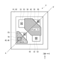
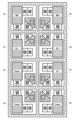
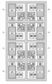
- FIG. 2 is a diagram showing an arrangement example of pixels of the imaging device according to the first embodiment.
- a pixel P of the imaging device 1 has a photoelectric conversion unit 12 and a lens 21 .
- the direction of incidence of light from a subject is the Z-axis direction
- the left-right direction of the paper surface orthogonal to the Z-axis direction is the X-axis direction
- the Z-axis direction and the vertical direction of the paper surface orthogonal to the X-axis direction is Y Axial direction.
- directions may be indicated with reference to the directions of the arrows in FIG.
- the lens 21 is an optical member also called an on-chip lens.
- the lens 21 is provided above the photoelectric conversion unit 12 for each pixel P or for each plurality of pixels P, for example.
- Light from a subject enters the lens 21 via an optical system such as an imaging lens.
- the photoelectric conversion unit 12 photoelectrically converts light incident through the lens 21 .
- the pixel P may have a filter 22 (see also FIG. 11, which will be described later).
- the filter 22 is configured to selectively transmit light in a specific wavelength range among incident light.
- the filter 22 is, for example, an RGB color filter, a filter that transmits infrared light, or the like.
- the plurality of pixels P provided in the pixel unit 100 of the imaging device 1 includes a plurality of pixels (R pixels) provided with a filter 22 that transmits red (R) light and a plurality of pixels (R pixels) that transmit green (G) light. and a plurality of pixels (B pixels) provided with filters 22 that transmit blue (B) light.
- a plurality of R pixels, a plurality of G pixels, and a plurality of B pixels are repeatedly arranged.
- the R pixels, G pixels, and B pixels are arranged, for example, according to the Bayer array.
- R pixels, G pixels, and B pixels can each be arranged in units of 2 ⁇ 2 pixels.
- R pixels, G pixels, and B pixels can each be arranged in units of 2 ⁇ 2 pixels.
- the pixel section 100 four adjacent R pixels, four adjacent G pixels, and four adjacent B pixels are repeatedly arranged. It can also be said that the R pixels, the G pixels, and the B pixels are periodically arranged in 2 rows ⁇ 2 columns.
- the R pixel, G pixel, and B pixel generate an R component pixel signal, a G component pixel signal, and a B component pixel signal, respectively.
- the imaging device 1 can obtain RGB pixel signals. Note that the arrangement of pixels is not limited to the example described above, and can be set arbitrarily.
- the filters 22 provided in the pixels P of the pixel unit 100 are not limited to primary color (RGB) color filters, and may be complementary color filters such as Cy (cyan), Mg (magenta), and Ye (yellow).
- Cy cyan
- Mg magenta
- Ye yellow
- a filter corresponding to W white
- W white
- the filter 22 may be omitted as necessary.
- the filter 22 may not be provided in the pixels P that receive white (W) light and perform photoelectric conversion. Further, the filter 22 may not be provided for some or all of the pixels P of the imaging device 1 .
- FIG. 3 is a diagram for explaining an example of a pixel circuit configuration of the imaging device according to the first embodiment.
- the pixel P of the imaging device 1 has a photoelectric conversion unit 12 (photoelectric conversion element), a transfer transistor TR, a floating diffusion FD, and a readout circuit 20 .
- the photoelectric conversion unit 12 is configured to receive light and generate a signal.
- the photoelectric conversion unit 12 is a light receiving unit (light receiving element), and is configured to generate electric charge by photoelectric conversion.
- the readout circuit 20 is configured to be able to output a signal based on photoelectrically converted charges.
- the readout circuit 20 is provided for a plurality of pixels P.
- the imaging device 1 has a configuration in which a plurality of pixels P share one readout circuit 20 . This makes it possible to reduce the number of elements (for example, the number of transistors) per pixel P (or one photoelectric conversion unit 12).
- the imaging device 1 can have a structure that is advantageous for miniaturization of pixels.
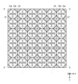
- the readout circuit 20 is arranged for every four pixels P (referred to as pixels Pa to Pd).
- Pixel Pa, pixel Pb, pixel Pc, and pixel Pd share one readout circuit 20 .
- 2 ⁇ 2 pixels composed of adjacent pixels Pa to Pd share one readout circuit 20 .
- the imaging device 1 can read out pixel signals of each of 2 ⁇ 2 pixels by operating the readout circuit 20 in a time-division manner.
- the imaging device 1 can also read a pixel signal obtained by adding each signal of 2 ⁇ 2 pixels.
- the photoelectric conversion unit 12 is a photodiode (PD), which converts incident light into charges.
- the photoelectric conversion unit 12 (in FIG. 3, the photodiode PD of the pixel Pa to the photodiode PD of the pixel Pd) performs photoelectric conversion to generate charges according to the amount of received light.
- the transfer transistor TR (in FIG. 3, the transfer transistor TR of the pixel Pa to the transfer transistor TR of the pixel Pd) is configured to be capable of transferring charges photoelectrically converted by the photoelectric conversion unit 12 to the floating diffusion FD.
- the transfer transistor TR is controlled by a signal STR and electrically connects or disconnects the photoelectric conversion section 12 and the floating diffusion FD.
- the transfer transistor TR can transfer the charges photoelectrically converted and accumulated in the photoelectric conversion unit 12 to the floating diffusion FD.
- the transfer transistors TR of the pixels Pa to Pd are on/off controlled by signals different from each other.
- the transfer transistor TR of pixel Pa is controlled by signal STR1
- the transfer transistor TR of pixel Pb is controlled by signal STR2.
- the transfer transistor TR of the pixel Pc is controlled by the signal STR3
- the transfer transistor TR of the pixel Pd is controlled by the signal STR4.
- the floating diffusion FD is an accumulation section, and is configured to be able to accumulate transferred charges.
- the floating diffusion FD can accumulate charges photoelectrically converted by the photoelectric conversion unit 12 .
- the floating diffusion FD can also be said to be a holding section capable of holding transferred charges.
- the floating diffusion FD accumulates the transferred charge and converts it into a voltage corresponding to the capacitance of the floating diffusion FD.
- the readout circuit 20 has an amplification transistor AMP, a selection transistor SEL, and a reset transistor RST, as shown in FIG.
- the amplification transistor AMP is configured to generate and output a signal based on the charges accumulated in the floating diffusion FD.
- the gate of the amplification transistor AMP is electrically connected to the floating diffusion FD of each pixel P, and receives the voltage converted by the floating diffusion FD.
- the drain of the amplification transistor AMP is connected to the power line to which the power supply voltage VDD is supplied, and the source of the amplification transistor AMP is connected to the signal line L2 via the selection transistor SEL.
- the amplification transistor AMP can generate a signal based on the charge accumulated in the floating diffusion FD, that is, a signal based on the voltage of the floating diffusion FD, and output it to the signal line L2.
- the selection transistor SEL is configured to be able to control the output of the pixel signal.
- the selection transistor SEL is controlled by a signal SSEL, and configured to output a signal from the amplification transistor AMP to the signal line L2.
- the selection transistor SEL can control the output timing of the signal of the pixel. Note that the selection transistor SEL may be provided between the power supply line to which the power supply voltage VDD is applied and the amplification transistor AMP. Also, the selection transistor SEL may be omitted as necessary.
- the reset transistor RST is configured to be able to reset the voltage of the floating diffusion FD.
- the reset transistor RST is electrically connected to a power supply line to which the power supply voltage VDD is applied, and configured to reset the charge of the pixel P.
- VDD power supply voltage
- the reset transistor RST can be controlled by a signal SRST to reset the charge accumulated in the floating diffusion FD and reset the voltage of the floating diffusion FD. Note that the reset transistor RST can discharge charges accumulated in the photoelectric conversion unit 12 via the transfer transistor TR.
- FIG. 4A is a diagram for explaining another example of the pixel circuit configuration of the imaging device according to the first embodiment.
- the readout circuit 20 may have a transistor FDG, as in the example shown in FIG. 4A.
- the transistor FDG is, for example, configured to be electrically connectable between the floating diffusion FD and the reset transistor RST.
- the transistor FDG is controlled by a signal SFDG to electrically connect or disconnect the floating diffusion FD and the reset transistor RST.
- the transistor FDG is a switching transistor that switches the capacitance connected to the gate of the amplification transistor AMP to change the conversion efficiency.
- the transistor FDG may be connected in series with the reset transistor RST, or may be connected in parallel with the reset transistor RST.
- the transistor FDG may be configured such that the floating diffusion FD and the capacitive element C1 can be electrically connected as in the example shown in FIG. 4B.
- the transistor FDG is controlled by a signal SFDG to electrically connect or disconnect the floating diffusion FD and the capacitive element C1. By switching the connection state of the capacitive element C1, it is possible to change the conversion efficiency.
- the above-described transfer transistor TR, amplification transistor AMP, selection transistor SEL, transistor FDG (switching transistor), and reset transistor RST are MOS transistors (MOSFETs) having gate, source, and drain terminals, respectively.
- the transfer transistor TR, amplification transistor AMP, selection transistor SEL, transistor FDG, and reset transistor RST are each composed of an NMOS transistor.
- the transistor of the pixel P may be configured by a PMOS transistor.
- the transistors of the pixel P (the transfer transistor TR, the amplification transistor AMP, the selection transistor SEL, the transistor FDG, the reset transistor RST, etc.) may be 3D transistors such as Fin-type transistors (Fin FETs).
- the pixel driving unit 111 (see FIG. 1) supplies a control signal to the gates of the transfer transistor TR, the selection transistor SEL, the transistor FDG, the reset transistor RST, etc. of each pixel P via the control line L1 described above, thereby turning the transistor on. It is on state (conducting state) or off state (non-conducting state).
- the plurality of control lines L1 of the imaging device 1 include wiring for transmitting a signal STR for controlling the transfer transistor TR, wiring for transmitting a signal SSEL for controlling the selection transistor SEL, wiring for transmitting a signal SFDG for controlling the transistor FDG, Wirings and the like for transmitting a signal SRST for controlling the reset transistor RST are included.
- the transfer transistor TR, the selection transistor SEL, the transistor FDG, the reset transistor RST, etc. are on/off controlled by the pixel driving section 111 .
- the pixel drive unit 111 controls the readout circuit 20 of each pixel P to output a pixel signal from each pixel P to the signal line L2.
- the pixel driving section 111 can perform control to read the pixel signal of each pixel P to the signal line L2.
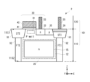
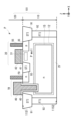
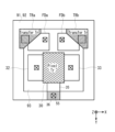
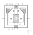
- FIG. 5 is a diagram showing an example of a planar configuration of pixels of the imaging device according to the first embodiment.
- 6 and 7 are diagrams for explaining an example of a cross-sectional configuration of a pixel of the imaging device.
- FIG. 6 shows a configuration example of a pixel in the direction of line A-A' shown in FIG.
- FIG. 7 shows a configuration example of a pixel in the direction of line B-B' shown in FIG.
- Each pixel P of the imaging device 1 has, for example, the structure shown in FIGS.
- the pixel P has a photoelectric conversion unit 12 , a transfer transistor TR, a floating diffusion FD, a pixel transistor 30 and a semiconductor region 35 .
- the pixel transistor 30 is, for example, the transistor of the readout circuit 20 described above.
- the pixel transistor 30 is used as an amplification transistor AMP, a selection transistor SEL, a transistor FDG, a reset transistor RST, or the like. Note that the pixel transistors 30 of some of the pixels P may be dummy transistors.
- the readout circuit 20 may include dummy transistors as the pixel transistors 30 .
- Each transistor such as the amplification transistor AMP, the selection transistor SEL, the transistor FDG, and the reset transistor RST of the readout circuit 20 is, for example, separately provided for a plurality of pixels P as a pixel transistor 30 and shared by the plurality of pixels P.
- the imaging device 1 By configuring the imaging device 1 in this manner, the number of transistors in one pixel P can be reduced.
- the imaging device 1 is configured using a substrate 101 including a semiconductor layer 110 .
- the substrate 101 is composed of, for example, a semiconductor substrate such as a Si (silicon) substrate.
- the substrate 101 including the semiconductor layer 110 is formed with, for example, the photoelectric conversion unit 12 and the readout circuit 20 described above.
- the substrate 101 may be configured using an SOI (Silicon On Insulator) substrate, a SiGe (Silicon Germanium) substrate, other compound semiconductor materials, or the like.
- SOI Silicon On Insulator
- SiGe Silicon Germanium
- the substrate 101 includes a semiconductor layer 110 and a wiring layer 120.
- the semiconductor layer 110 has a first surface 11S1 and a second surface 11S2 facing each other, as shown in FIGS.
- the second surface 11S2 is a surface opposite to the first surface 11S1.
- the first surface 11S1 of the semiconductor layer 110 is an element formation surface on which elements such as transistors are formed.
- a gate electrode, a gate oxide film, and the like are provided on the first surface 11S1 of the semiconductor layer 110 .
- the second surface 11S2 of the semiconductor layer 110 is a light receiving surface (light incident surface).
- a plurality of photoelectric conversion units 12 are provided in the semiconductor layer 110.
- a plurality of photoelectric conversion units 12 are embedded in the semiconductor layer 110 .
- the semiconductor layer 110 has wells 25, as shown in FIGS.
- the well 25 is, for example, a p-type semiconductor region and is a p-type well (p-well).
- the semiconductor layer 110 is provided with a well 25 that is a p-type well region.
- the photoelectric conversion section 12 is configured including a semiconductor region 15 provided within the well 25 .
- the semiconductor region 15 is, for example, an n-type semiconductor region.
- a transfer transistor TR, a floating diffusion FD, a pixel transistor 30, a semiconductor region 35, and the like are provided on the first surface 11S1 side of the semiconductor layer 110 .
- the floating diffusion FD includes, for example, an n-type semiconductor region, as shown in FIG.
- the imaging device 1 is provided with trenches 91 and 92 as shown in FIGS.
- the trenches 91 and 92 are each provided between a plurality of adjacent pixels P in the semiconductor layer 110 .
- the trenches 91 and 92 are provided between the photoelectric conversion units 12 of a plurality of adjacent pixels P to separate the pixels P (or the photoelectric conversion units 12). It can also be said that the pixel P has a structure partitioned by the trenches 91 and 92 .
- the trenches 91 and 92 are isolation portions (groove portions), respectively, and are configured using an insulating material, for example. At least a portion of each of the trenches 91 and 92 is provided at the boundary between adjacent pixels P. As shown in FIG.
- the trench 91 has an STI (Shallow Trench Isolation) structure and is provided on the first surface 11S1 side of the semiconductor layer 110 .
- the trench 92 has an FTI (Full Trench Isolation) structure and is provided to penetrate the semiconductor layer 110 .
- the trench 91 is provided in the semiconductor layer 110 so as to surround the transfer transistor TR, the floating diffusion FD, the pixel transistor 30, the semiconductor region 35, and the like.
- the trench 92 is provided in the semiconductor layer 110 so as to surround the photoelectric conversion section 12 .
- the trenches 91 and 92 are provided in a lattice shape so as to surround each photoelectric conversion unit 12 of each pixel P in plan view.
- the trenches 91 and 92 can also be called inter-pixel isolation portions or inter-pixel isolation walls.
- An insulating film such as an oxide film (for example, a silicon oxide film) or a nitride film (for example, a silicon nitride film) is provided in the trenches 91 and 92 .
- the trenches 91 and 92 may be filled with polysilicon, metal material, or the like. Further, voids (cavities) may be provided in the trenches 91 and 92 .
- Trench 92 may be formed within trench 91 .
- the trench 92 may extend from the trench 91 provided on the first surface 11S1 side of the semiconductor layer 110 to the second surface 11S2 of the semiconductor layer 110 .
- the imaging device 1 is provided with a trench 93 .
- the trench 93 is an isolation portion (trench portion) having an STI structure.
- An insulating film such as an oxide film (for example, a silicon oxide film) or a nitride film (for example, a silicon nitride film) is provided in the trench 93 .
- the trench 93 is provided on the first surface 11S1 side of the semiconductor layer 110 and isolates the elements.
- the trench 93 can be formed between the pixel transistor 30 and the floating diffusion FD, between the transfer transistor TR and the semiconductor region 35, or the like.
- the semiconductor region 35 is provided on the first surface 11S1 side of the semiconductor layer 110 .
- the semiconductor region 35 is a semiconductor region of the same conductivity type as the well 25 .
- the semiconductor region 35 is provided in the well 25 and electrically connected with the well 25 .
- the semiconductor region 35 is, for example, a p-type semiconductor region formed using p-type impurities.
- the semiconductor region 35 has, for example, an impurity concentration higher than that of the well 25, and is a p+ type semiconductor region.
- the semiconductor region 35 which is a p+ region, is a p+ type diffusion region and can also be called a p+ type conductive region. Also, the semiconductor region 35 is electrically connected to a contact 55 provided in the wiring layer 120 .
- the semiconductor region 35 is connected to a contact 55 provided on the semiconductor region 35 and electrically connected to the wiring (not shown) of the wiring layer 120 via the contact 55 .
- Contact 55 is electrically connected to well 25 by semiconductor region 35 .
- the contact 55 is, for example, ohmic-connected to the semiconductor region 35 and electrically connected to the well 25 via the semiconductor region 35 .
- a region of the well 25 electrically connected to the semiconductor region 35 is supplied with a predetermined potential (voltage) through the wiring of the wiring layer 120, the contact 55, and the like.
- the contact 55 is a well contact, and the semiconductor region 35 is a well contact region.
- the contact 55 and the semiconductor region 35 are arranged for each pixel P, for example.
- the semiconductor region 35 and the contact 55 can be collectively called a well contact region.
- the semiconductor region 35 is, for example, electrically connected to a reference potential line in the wiring layer 120 via the contact 55, and the semiconductor region 35 and the well 25 are supplied with the reference potential.
- a GND potential ground potential
- the pixel transistor 30 has a semiconductor region 31 , a semiconductor region 32 , a semiconductor region 33 , a gate insulating film 41 and a gate electrode 42 .
- the semiconductor regions 31 to 33 are provided in the well 25, respectively. It can also be said that the semiconductor regions 32 and 33 and the like are arranged to replace part of the well 25 .
- the semiconductor region 31 and the semiconductor region 32 (or the semiconductor region 33) have conductivity types different from each other.
- the semiconductor region 31 is a region (channel region) in which a channel is formed.
- the semiconductor region 31 is a p-type semiconductor region formed using p-type impurities.
- the semiconductor region 31 is a p-type diffusion region and can also be called a p-type conductive region.
- the semiconductor regions 32 and 33 are the source and drain regions of the pixel transistor 30 .
- One of the semiconductor regions 32 and 33 is the source region of the pixel transistor 30 and the other of the semiconductor regions 32 and 33 is the drain region of the pixel transistor 30 .
- the semiconductor region 32 and the semiconductor region 33 are, for example, n-type semiconductor regions, respectively, and are regions formed using n-type impurities.
- the semiconductor regions 32 and 33 are formed, for example, by doping (adding) n-type impurities to regions of the semiconductor layer 110 .
- the semiconductor regions 32 and 33 are n-type diffusion regions, respectively, and can also be called n-type conductive regions.
- the semiconductor region 32 is connected to a contact 52 provided on the semiconductor region 32 and electrically connected to wiring (not shown) of the wiring layer 120 via the contact 52 .
- the semiconductor region 33 is connected to a contact 53 provided on the semiconductor region 33 and electrically connected to the wiring of the wiring layer 120 via the contact 53 .
- a semiconductor region 32 and a semiconductor region 33 are arranged around the gate electrode 42 of the pixel transistor 30 .
- a pixel transistor 30 having semiconductor regions 32 and 33 is formed in a region around the transfer transistor TR.
- the pixel transistor 30 has an L-shaped shape in plan view. Note that the shape of the pixel transistor 30 is not limited to the example shown in FIG. 5 and the like, and can be changed as appropriate.
- the gate insulating film 41 of the pixel transistor 30 is provided on the channel region (semiconductor region 31 ) of the semiconductor layer 110 .
- a gate insulating film 41 (for example, a gate oxide film) is provided between the semiconductor region 31 which is a channel region and the gate electrode 42 .
- a gate electrode 42 is provided on the gate insulating film 41 .
- the gate electrode 42 is provided above the semiconductor region 31 of the semiconductor layer 110 with the gate insulating film 41 interposed therebetween.
- the transfer transistor TR has a gate insulating film 45 and a gate electrode 46 . At least part of each of the gate insulating film 45 and the gate electrode 46 of the transfer transistor TR is provided in the semiconductor layer 110 . At least part of each of the gate insulating film 45 and the gate electrode 46 is provided by digging the semiconductor layer 110 as in the example shown in FIG. 7 and the like.
- the transfer transistor TR has, for example, a vertical gate structure. The transfer transistor TR can also be said to be a vertical transistor.
- the transfer transistor TR may have a planar gate structure.
- the transfer transistor TR may be a planar transistor.
- each of the gate electrode 46 and the gate insulating film 45 of the transfer transistor TR is arranged so as to be embedded in the semiconductor layer 110, for example.
- the gate electrode 46 can be provided in the semiconductor layer 110 from between the floating diffusion FD and the trench 91 to the region of the photoelectric conversion section 12 .
- the gate insulating film 45 is formed along the gate electrode 46 within the semiconductor layer 110 .
- the gate insulating film 41 of the pixel transistor 30 and the gate insulating film 45 of the transfer transistor TR are single layers made of, for example, one of silicon oxide (SiO), silicon oxynitride (SiON), hafnium oxide (HfO), and the like. It is formed of a film or a laminated film composed of two or more of these.
- the gate insulating films 41 and 45 can be made of a high dielectric constant material having a dielectric constant higher than that of silicon oxide, such as a hafnium-based insulating film.
- the gate electrode 42 of the pixel transistor 30 and the gate electrode 46 of the transfer transistor TR are made of polysilicon (Poly-Si), for example. Gate electrodes 42 and 46 may be constructed using a metallic material or metallic compound. The gate electrodes 42 and 46 may be made of, for example, titanium nitride (TiN), tantalum nitride (TaN), tungsten, or the like.
- the contacts 52, 53, and 55 are each constructed using a conductive material.
- the contacts 52, 53 and 55 are each formed by embedding (filling) the contact holes with a conductive material such as tungsten (W).
- a conductive material such as tungsten (W).
- Each of the contacts 52, 53, 55 may be made of a metal material such as aluminum (Al) or copper (Cu), or may be made of another material.
- the semiconductor region 35 is provided in contact with the pixel transistor 30 .
- the semiconductor region 35 is arranged in contact with the source region or the drain region of the pixel transistor 30 in the pixel P, for example.
- the semiconductor region 35 is arranged in contact with the semiconductor region 33 of the pixel transistor 30 on the first surface 11S1 side of the semiconductor layer 110 .
- contact includes direct contact and contact via a natural oxide film or the like.
- the semiconductor region 35 and the semiconductor region 33 are in contact includes the case where a natural oxide film intervenes and the case where the semiconductor region 35 is in contact with the semiconductor region 33 via a thin natural oxide film.
- the term “in contact with” means that an insulating film functioning as an STI (Shallow Trench Isolation), an impurity region functioning as a channel stop region (functioning differently from the semiconductor regions 33 and 35), or a well region between the semiconductor regions. Indicates none. However, when the N-type semiconductor region 33 and the P-type semiconductor region 35 are in contact with each other, a layer depleted by the PN junction is formed at the interface.
- the semiconductor region 35 is provided, for example, in contact with the side surface (side portion) of the semiconductor region 33 which is the source region or drain region of the pixel transistor 30 . Note that the semiconductor region 35 may be provided in contact with the semiconductor region 32 . The semiconductor region 35 may be provided adjacent to the gate of the pixel transistor 30 .
- the semiconductor region 35 is provided in contact with the pixel transistor 30 . Therefore, the imaging device 1 can have a structure that is advantageous for miniaturization. Compared to the case where the semiconductor region 35 and the pixel transistor 30 are provided apart from each other, the area of the region where the transistor or the like is arranged in the pixel P can be increased. The size of the transistor arranged in the pixel P can be increased.
- the present embodiment it is possible to increase the area of the pixel transistor 30 as in the example shown in FIG. It is possible to increase the size of the transistor of the readout circuit 20, for example, the amplification transistor AMP, and to suppress the noise mixed in the pixel signal.
- the area efficiency of fine pixels can be improved, and the size of the pixel transistor 30 (eg, gate length, gate width, etc.) can be increased. Therefore, it is possible to improve the characteristics of the transistors (the amplification transistor AMP, the selection transistor SEL, the transistor FDG, the reset transistor RST, etc.) of the readout circuit 20 . As a result, it is possible to suppress the deterioration of the quality of the pixel signal, and it is possible to suppress the deterioration of the image quality of the image.
- the transistors the amplification transistor AMP, the selection transistor SEL, the transistor FDG, the reset transistor RST, etc.
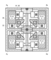
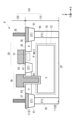
- FIG. 8 is a diagram showing an arrangement example of pixel transistors of the imaging device according to the first embodiment.
- 2 ⁇ 2 pixels are illustrated with four pixels P sharing the readout circuit 20 as pixels Pa to Pd.
- Other pixels P in the imaging device 1 may also have the same configuration as the configuration shown in FIG.
- an amplification transistor AMP is provided as the pixel transistor 30 in the pixel Pa.
- a selection transistor SEL is provided as the pixel transistor 30 in the pixel Pb.
- a reset transistor RST is provided as the pixel transistor 30 in the pixel Pc.
- a dummy transistor is provided as the pixel transistor 30 in the pixel Pd.
- a wiring L3 is provided.
- Each floating diffusion FD of a plurality of pixels P sharing the readout circuit 20 is electrically connected to the transistor of the readout circuit 20 via the wiring L3.
- the floating diffusion FD of each of the pixels Pa to Pd is electrically connected to the gate electrode of the amplification transistor AMP, which is the pixel transistor 30 of the pixel Pa, via the wiring L3.
- the wiring L3 is a wiring shared by the four pixels Pa to Pd.
- the wiring L3 is formed using, for example, a metal material such as aluminum (Al) or tungsten (W).
- the wiring L3 may be made of polysilicon (Poly-Si) or another conductive material.
- FIG. 9 and 10 are diagrams showing another arrangement example of the pixel transistors of the imaging device according to the first embodiment.
- Each transistor of the readout circuit 20 may be arranged as shown in FIG. 9 or 10 .
- the readout circuit 20 has an amplification transistor AMP, a selection transistor SEL, a reset transistor RST, and a transistor FDG.
- the pixel Pa has an amplification transistor AMP as the pixel transistor 30.
- the pixel Pb has a selection transistor SEL as the pixel transistor 30 .
- the pixel Pc has a reset transistor RST as the pixel transistor 30 .
- the pixel Pd has a transistor FDG as the pixel transistor 30 .
- the readout circuit 20 may have a plurality of amplification transistors AMP (amplification transistor AMP1 and amplification transistor AMP2 in FIG. 10) connected in parallel.
- amplification transistor AMP1 is arranged in the pixel Pa
- the amplification transistor AMP2 is arranged in the pixel Pb.
- the readout circuit 20 can generate and output a pixel signal by the amplification transistors AMP1 and AMP2 connected in parallel. Therefore, it is possible to reduce noise mixed in the pixel signal.
- FIG. 11 is a diagram showing an example of the cross-sectional configuration of the imaging device according to the first embodiment.
- the imaging device 1 has a configuration in which a light guide section 90, a semiconductor layer 110, and a wiring layer 120 are stacked in the Z-axis direction.
- the wiring layer 120 is provided on the first surface 11S1 side of the semiconductor layer 110 .
- a light guide portion 90 is provided on the second surface 11S2 side of the semiconductor layer 110 .
- a light guide portion 90 is provided on the side on which light from the optical system is incident, and a wiring layer 120 is provided on the side opposite to the side on which the light is incident.
- the imaging device 1 is a so-called back-illuminated imaging device.
- the wiring layer 120 includes, for example, a conductor film and an insulating film, and has a plurality of wirings and vias (VIAs).
- the wiring layer 120 includes, for example, two or more layers of wiring.
- the wiring layer 120 may include wiring of five or more layers.
- the wiring layer 120 has a structure in which a plurality of wirings are stacked with insulating films interposed therebetween.
- the insulating film of the wiring layer 120 can also be called an interlayer insulating film (interlayer insulating layer).
- the wiring of the wiring layer 120 is formed using metal materials such as aluminum (Al), copper (Cu), and tungsten (W).
- the wiring of the wiring layer 120 may be configured using polysilicon (Poly-Si) or other conductive materials.
- the interlayer insulating film is formed using, for example, silicon oxide (SiO), silicon nitride (SiN), silicon oxynitride (SiON), or the like.
- the semiconductor layer 110 and the wiring layer 120 are provided with, for example, the photoelectric conversion section 12, the readout circuit 20, etc., as described above.
- the pixel driving unit 111 , the signal processing unit 112 , the control unit 113 , the processing unit 114 and the like described above can be provided on a substrate different from the semiconductor layer 110 or on the semiconductor layer 110 and the wiring layer 120 .
- the trenches 91 and 92 are provided between adjacent photoelectric conversion units 12 to separate the photoelectric conversion units 12 from each other.
- the trenches 91 and 92 are provided in the semiconductor layer 110 so as to surround the photoelectric conversion section 12 .
- the trenches 91 and 92 are formed in a grid pattern in a plan view, and arranged so as to surround each of the plurality of photoelectric conversion units 12 .
- the light guide part 90 shown in FIG. 11 is stacked on the semiconductor layer 110 in the thickness direction orthogonal to the second surface 11S2 of the semiconductor layer 110. As shown in FIG.
- the light guide section 90 has a lens 21 and a filter 22 and guides incident light to the semiconductor layer 110 side.
- the lens 21 is provided on the filter 22 for each pixel P or for each plurality of pixels P, for example.
- Light from a subject enters the lens 21 via an optical system such as an imaging lens.
- the photoelectric conversion unit 12 photoelectrically converts light incident through the lens 21 and the filter 22 .
- the imaging device 1 is provided with a light blocking section 23 as shown in FIG.
- the light shielding portion 23 (light shielding film) is configured by a member that shields light, and is provided at the boundary between a plurality of pixels P adjacent to each other.
- the light shielding part 23 (light shielding member) is provided, for example, between adjacent filters 22 and can be positioned at the boundary between the adjacent filters 22 .
- the light shielding part 23 is made of, for example, a metal material (aluminum (Al), tungsten (W), copper (Cu), etc.) that shields light.
- the light shielding part 23 may be made of a material that absorbs light.
- the imaging device 1 may have an antireflection film and a fixed charge film.
- a fixed charge film is provided, for example, between the semiconductor layer 110 and the filter 22 .
- the fixed charge film is made of, for example, a metal compound (metal oxide, metal nitride, etc.).
- the fixed charge film is, for example, a film having negative fixed charges, and suppresses generation of dark current at the interface of the semiconductor layer 110 .
- the antireflection film is configured using an insulating material such as silicon nitride (SiN) or silicon oxide (SiO).
- An antireflection film is provided, for example, between the semiconductor layer 110 and the filter 22 to reduce (suppress) reflection.
- the photodetector includes a semiconductor layer (semiconductor layer 110) and a plurality of pixels including a first pixel (for example, pixel Pa) having a photoelectric conversion element (photoelectric conversion unit 12) provided in the semiconductor layer. and trenches (trench 91, trench 92) provided between a plurality of adjacent pixels in the semiconductor layer.
- the first pixel includes a transistor (pixel transistor 30) provided on the first surface side of the semiconductor layer, a first conductivity type first semiconductor region (semiconductor region 35) provided on the first surface side of the semiconductor layer, and a first contact (contact 55) electrically connected to one semiconductor region. The first semiconductor region is in contact with the transistor.
- the semiconductor region 35 is in contact with the pixel transistor 30 in the photodetector (imaging device 1) according to the present embodiment.
- the semiconductor region 35 is provided in contact with the semiconductor region 33 which is the source region or drain region of the pixel transistor 30 . Therefore, the imaging device 1 can have a structure that is advantageous for miniaturization of pixels.
- the size of the pixel transistor can be increased, and the characteristics of the pixel transistor can be improved. It is possible to realize a photodetector that is advantageous for miniaturization.
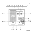
- FIG. 12 is a diagram illustrating an example of a planar configuration of pixels of an imaging device according to Modification 1 of the present disclosure.
- FIG. 13 is a diagram for explaining an example of a cross-sectional configuration of pixels of an imaging device.
- FIG. 13 schematically shows a configuration example of a pixel in the direction of line AA' shown in FIG.
- a conductor region 36 is provided.
- a conductor region 36 is provided around the semiconductor region 35 . At least part of the conductor region 36 is provided in contact with the semiconductor region 35 .
- the conductor region 36 is formed adjacent to the semiconductor region 35 on the first surface 11S1 side of the semiconductor layer 110 . In the example shown in FIG. 13, the conductor region 36 is positioned above the interior of the trenches 91 and 92 .
- the conductor region 36 is made of, for example, polysilicon doped (added) with impurities. Note that the conductor region 36 (conductive portion) may be configured using another conductive material (for example, a metal material or the like). The conductor region 36 has an impurity concentration higher than that of the well 25, for example.
- a contact 55 is provided on the conductor region 36 .
- Contact 55 is electrically connected to semiconductor region 35 and well 25 through conductor region 36 .
- the semiconductor region 35 provided in the well 25 and the contact 55 are electrically connected via the conductor region 36 . Therefore, the impurity concentration of the semiconductor region 35 required for electrical connection with the contact 55 can be reduced.
- FIG. 14 is a diagram showing an example of a planar configuration of an imaging device according to Modification 1.
- FIG. FIG. 15 is a diagram for explaining an example of a cross-sectional configuration of an imaging device.
- a conductor region 36 may be provided as in the examples shown in FIGS. 14 and 15 . At least part of the conductor region 36 is provided at the boundary between the adjacent pixels P. As shown in FIG.
- Each semiconductor region 33 of a plurality of adjacent pixels P is electrically connected to contacts 55 via common conductor regions 36 .
- Conductor region 36 is provided in semiconductor layer 110, as described above. In the examples shown in FIGS. 13, 15, etc., the conductor region 36 is arranged above in the trench 91 . Therefore, it is possible to prevent unnecessary parasitic capacitance from occurring in the imaging device 1 . For example, it is possible to avoid adding unnecessary parasitic capacitance to the transistor of the readout circuit 20 .
- FIG. 16 and 17 are diagrams for explaining another example of the cross-sectional configuration of the pixels of the imaging device according to Modification 1.
- a conductor region 36 may be provided on the first surface 11S1 of the semiconductor layer 110. As shown in FIG. In the example shown in FIG. 16, the conductor region 36 is provided within the wiring layer 120 . A part of the conductor region 36 may be provided in the semiconductor layer 110 as in the example shown in FIG. 17 . A portion of conductor region 36 may be formed within trench 91 .
- (1-2. Modification 2) 18 is a diagram illustrating an example of a planar configuration of pixels of an imaging device according to Modification 2.
- FIG. FIG. 19 is a diagram for explaining an example of a planar configuration of an imaging device according to Modification 2.
- the imaging device 1 may have a semiconductor region 37 as shown in FIGS. 18 and 19 .
- the semiconductor region 37 is provided around the floating diffusion FD in the semiconductor layer 110 .
- the semiconductor region 37 is made of polysilicon doped with impurities, for example. Note that the semiconductor region 37 may be configured using another conductive material. At least part of the semiconductor region 37 is provided in contact with the floating diffusion FD.
- the floating diffusions FD of the plurality of pixels P (pixels Pa to pixel Pd in FIG. 19) sharing the readout circuit 20 are electrically connected to each other via the semiconductor region 37 .
- the floating diffusion FD of each of the pixels Pa to Pd is electrically connected through the semiconductor region 37 to the amplification transistor AMP, reset transistor RST, etc. of the readout circuit 20 .
- FIG. 21 is a diagram for explaining an example of a cross-sectional configuration of a pixel of an imaging device; FIG. 21 schematically shows a configuration example of a pixel in the direction of line AA' shown in FIG.
- the semiconductor region 35 may be provided adjacent to at least one of the gate electrode 42 and the gate insulating film 41 of the pixel transistor 30 in the pixel P.
- the semiconductor region 35 is arranged adjacent to the gate insulating film 41 and the gate electrode 42 of the pixel transistor 30 on the first surface 11S1 side of the semiconductor layer 110 .
- “adjacent” includes cases where they are not in contact with each other. "Adjacent” includes the case of being in direct contact and the case of being adjacent via a natural oxide film or the like.
- the imaging device 1 can have a structure that is advantageous for miniaturization. Compared to the case where the semiconductor region 35 and the pixel transistor 30 are arranged apart from each other, the area of the region where the transistor and the like are arranged in the pixel P can be increased. The size of the pixel transistor 30 arranged in the pixel P can be increased, and the characteristics of the amplification transistor AMP and the like of the readout circuit 20 can be improved.
- FIG. 22 is a diagram showing another example of the planar configuration of the pixels of the imaging device according to Modification 3.
- FIG. 23 and 24 are diagrams for explaining another example of the cross-sectional configuration of the pixels of the imaging device.
- FIGS. 23 and 24 schematically show examples of pixel configurations along the line A-A' shown in FIG.
- the imaging device 1 may have a conductor region 36 that electrically connects the contact 55 and the semiconductor region 35, as shown in FIGS.
- the conductor region 36 may be formed on the semiconductor layer 110 as in the example shown in FIG. A portion of the conductor region 36 may be provided within the semiconductor layer 110 .
- FIG. 25 is a diagram showing another example of the planar configuration of the pixels of the imaging device according to Modification 3.
- FIG. 26 and 27 are diagrams for explaining another example of the cross-sectional configuration of the pixels of the imaging device. 26 and 27 schematically show examples of the pixel configuration in the direction of line A-A' shown in FIG. 25, respectively.
- the imaging device 1 may have a semiconductor region 37 electrically connecting the floating diffusion FD of each of the plurality of pixels P, as shown in FIGS. 25 and 26 .
- the semiconductor region 37 may be formed on the semiconductor layer 110 as in the example shown in FIG. A portion of the semiconductor region 37 may be provided within the semiconductor layer 110 .
- FIGS. 28 to 35 are diagrams for explaining an arrangement example of pixel transistors of an imaging device according to Modification 4.
- FIG. 28 to 35 show examples in which 2 ⁇ 4 pixels share one readout circuit 20.
- the readout circuit 20 may have a plurality of amplification transistors AMP (amplification transistors AMP1 to AMP6, etc.) connected in parallel. Further, the readout circuit 20 may have a plurality of selection transistors SEL (for example, selection transistor SEL1 and selection transistor SEL2) connected in parallel.
- amplification transistors AMP amplification transistors AMP1 to AMP6, etc.
- selection transistors SEL for example, selection transistor SEL1 and selection transistor SEL2
- the pixel Pa is provided with an amplification transistor AMP1 as the pixel transistor 30.
- An amplification transistor AMP2 is provided as the pixel transistor 30 in the pixel Pb.
- a reset transistor RST is provided as the pixel transistor 30 in the pixel Pc.
- a selection transistor SEL is provided as the pixel transistor 30 in the pixel Pd.
- the pixel Pe is provided with a transistor FDG as the pixel transistor 30 .
- a dummy transistor is provided as the pixel transistor 30 in each of the pixels Pf to Ph.
- an amplification transistor AMP1 is provided as the pixel transistor 30 in the pixel Pa.
- An amplification transistor AMP2 is provided as the pixel transistor 30 in the pixel Pb.
- a selection transistor SEL1 is provided as the pixel transistor 30 in the pixel Pc.
- a selection transistor SEL2 is provided as the pixel transistor 30 in the pixel Pd.
- each of the pixels Pe, Pg, and Ph is provided with a dummy transistor as the pixel transistor 30 .
- a reset transistor RST is provided as the pixel transistor 30 in the pixel Pf.
- a transistor FDG is provided as the pixel transistor 30 in the pixel Pe.
- a reset transistor RST is provided as the pixel transistor 30 in the pixel Pf.
- a dummy transistor is provided as the pixel transistor 30 in each of the pixel Pg and the pixel Ph.
- a selection transistor SEL3 is provided as the pixel transistor 30 in the pixel Pe.
- a reset transistor RST is provided as the pixel transistor 30 in the pixel Pf.
- An amplification transistor AMP3 is provided as the pixel transistor 30 in the pixel Pg.
- a dummy transistor is provided as the pixel transistor 30 in the pixel Ph.
- a transistor FDG may be arranged as the pixel transistor 30 of the pixel Ph.
- an amplification transistor AMP1 is provided as the pixel transistor 30 in the pixel Pa.
- a selection transistor SEL1 is provided as the pixel transistor 30 in the pixel Pb.
- An amplification transistor AMP2 is provided as the pixel transistor 30 in the pixel Pc.
- a dummy transistor is provided as the pixel transistor 30 in the pixel Pd.
- the pixel Pe is provided with an amplification transistor AMP3 as the pixel transistor 30.
- a reset transistor RST is provided as the pixel transistor 30 in the pixel Pf.
- An amplification transistor AMP4 is provided as the pixel transistor 30 in the pixel Pg.
- a selection transistor SEL2 is provided as the pixel transistor 30 in the pixel Ph.
- a transistor FDG may be arranged as the pixel transistor 30 of the pixel Pd.
- an amplification transistor AMP1 is provided as the pixel transistor 30 in the pixel Pa.
- a selection transistor SEL is provided as the pixel transistor 30 in the pixel Pb.
- An amplification transistor AMP2 is provided as the pixel transistor 30 in the pixel Pc.
- an amplification transistor AMP5 is provided as the pixel transistor 30 in the pixel Pd.
- the pixel Pe is provided with an amplification transistor AMP3 as the pixel transistor 30.
- An amplification transistor AMP6 is provided as the pixel transistor 30 in the pixel Pf.
- an amplification transistor AMP4 is provided as the pixel transistor 30 in the pixel Pg.
- a reset transistor RST is provided as the pixel transistor 30 in the pixel Ph.
- FIG. 36 is a diagram showing an arrangement example of pixels of an imaging device according to the second embodiment of the present disclosure.
- the pixel P of the imaging device 1 has a plurality of photoelectric conversion units 12 (in the example shown in FIG. 36, photoelectric conversion units 12a and 12b).
- the photoelectric conversion unit 12b is provided next to the photoelectric conversion unit 12a. It can also be said that a pixel having the photoelectric conversion unit 12a and a pixel having the photoelectric conversion unit 12b are provided.
- one lens 21 (lens section) is provided for a plurality of photoelectric conversion sections 12, for example, two photoelectric conversion sections 12 (photoelectric conversion section 12a and photoelectric conversion section 12b).
- the photoelectric conversion unit 12a and the photoelectric conversion unit 12b receive light that has passed through mutually different regions of an optical system such as an imaging lens, and pupil division is performed.
- Phase difference data (phase difference information) is obtained by using the first pixel signal based on the charge photoelectrically converted by the photoelectric conversion unit 12a and the second pixel signal based on the charge photoelectrically converted by the photoelectric conversion unit 12b. can be obtained.
- Phase difference AF Auto Focus
- the readout circuit 20 is configured to be able to output the first pixel signal and the second pixel signal of each pixel P sharing the readout circuit 20 . Further, the readout circuit 20 can read out a pixel signal corresponding to the charge obtained by adding the charge converted by the photoelectric conversion unit 12a and the charge converted by the photoelectric conversion unit 12b.
- FIG. 37 is a diagram showing an example of a planar configuration of pixels of an imaging device according to the second embodiment.
- a pixel P of the imaging device 1 includes transfer transistors TRa and TRb, floating diffusions FDa and FDb, pixel transistors 30 a and 30 b, and a semiconductor region 35 .
- the transfer transistor TRa is configured to transfer the charge photoelectrically converted by the photoelectric conversion unit 12a to the floating diffusion FDa.
- the transfer transistor TRb is configured to be capable of transferring charges photoelectrically converted by the photoelectric conversion unit 12b to the floating diffusion FDb.
- the floating diffusion FDa can accumulate charges photoelectrically converted by the photoelectric conversion unit 12a.
- the floating diffusion FDb can accumulate charges photoelectrically converted by the photoelectric conversion unit 12b.
- the readout circuit 20 is configured to be able to output, for example, a pixel signal based on charges accumulated in the floating diffusion FDa, a pixel signal based on charges accumulated in the floating diffusion FDb, and the like. Further, for example, the readout circuit 20 is configured to be capable of outputting a pixel signal corresponding to the sum of the charge accumulated in the floating diffusion FDa and the charge accumulated in the floating diffusion FDb.
- the pixel transistor 30a and the pixel transistor 30b are transistors of the readout circuit 20, for example.
- the semiconductor regions 32a and 33a are the source and drain regions of the pixel transistor 30a.
- One of the semiconductor regions 32a and 33a is the source region of the pixel transistor 30a, and the other of the semiconductor regions 32a and 33a is the drain region of the pixel transistor 30a.
- the semiconductor region 32b and the semiconductor region 33b are the source region and the drain region of the pixel transistor 30b.
- One of the semiconductor regions 32b and 33b is the source region of the pixel transistor 30b, and the other of the semiconductor regions 32b and 33b is the drain region of the pixel transistor 30b.
- the pixel transistors 30a and 30b are each used as an amplification transistor AMP, a selection transistor SEL, a transistor FDG, a reset transistor RST, or the like. Note that the pixel transistors 30a or 30b of some of the pixels P may be dummy transistors.
- the readout circuit 20 may include a dummy transistor as the pixel transistor 30a or the pixel transistor 30b.
- the semiconductor region 35 is provided in contact with the pixel transistor 30a and the pixel transistor 30b.
- the semiconductor region 35 is arranged in contact with the source region or drain region of the pixel transistor 30a and the source region or drain region of the pixel transistor 30b.
- the semiconductor region 35 is provided in contact with the semiconductor region 33a of the pixel transistor 30a and the semiconductor region 33b of the pixel transistor 30b.
- the semiconductor region 35 may be provided in contact with the semiconductor regions 32a and 32b.
- the semiconductor region 35 may be provided adjacent to each gate of the pixel transistors 30a and 30b.
- the semiconductor region 35 is provided in contact with the pixel transistor 30a and the pixel transistor 30b. Therefore, the imaging device 1 can have a structure that is advantageous for miniaturization. Compared to the case where the semiconductor region 35 and the pixel transistors 30a and 30b are provided apart from each other, the area of the region where the transistors and the like are arranged in the pixel P can be increased. The size of the transistor arranged in the pixel P can be increased.
- FIG. 38 is a diagram showing another example of the planar configuration of the pixels of the imaging device according to the second embodiment.
- one pixel transistor 30 may be provided for each of the photoelectric conversion units 12a and 12b.
- the pixel transistor 30 is, for example, a transistor of the readout circuit 20 and arranged for each pixel P.
- the semiconductor region 35 is provided in contact with the source region or the drain region of the pixel transistor 30 in the pixel P, for example. In the example shown in FIG. 38 , the semiconductor region 35 is provided in contact with the semiconductor region 33 of the pixel transistor 30 . Also in this case, the size of the transistor arranged in the pixel P can be increased, and the characteristics of the amplification transistor AMP and the like of the readout circuit 20 can be improved.
- the area efficiency of fine pixels can be improved, and the size of the pixel transistor 30 can be increased. Therefore, it is possible to improve the characteristics of the transistors of the readout circuit 20 . It is possible to suppress the deterioration of the quality of the pixel signal, and it is possible to suppress the deterioration of the image quality of the image.
- the photodetector includes a semiconductor layer (semiconductor layer 110), a plurality of pixels including a first pixel having a photoelectric conversion element, and trenches (trench 91 and trench 92).
- the first pixel includes a transistor (pixel transistor 30), a first conductivity type first semiconductor region (semiconductor region 35), and a first contact (contact 55).
- the first semiconductor region is in contact with the transistor.
- the photodetector has a lens (lens 21) into which light is incident.
- the photodetector includes, as photoelectric conversion elements, a first photoelectric conversion element (photoelectric conversion unit 12a) that photoelectrically converts light transmitted through the lens, and a first photoelectric conversion element (photoelectric conversion unit 12a) provided next to the first photoelectric conversion element that converts light transmitted through the lens into a photoelectric conversion element. and a second photoelectric conversion element (photoelectric conversion unit 12b) for conversion.
- the semiconductor region 35 is in contact with the pixel transistor 30 in the photodetector (imaging device 1) according to the present embodiment. Therefore, the imaging device 1 can have a structure that is advantageous for miniaturization of pixels.
- the size of the pixel transistor can be increased, and the characteristics of the pixel transistor can be improved. It is possible to realize a photodetector that is advantageous for miniaturization.
- FIG. 39 is a diagram illustrating an example of a planar configuration of pixels of an imaging device according to Modification 5 of the present disclosure.
- FIG. 40 is a diagram for explaining an example of a cross-sectional configuration of a pixel of an imaging device; FIG. 40 schematically shows a configuration example of a pixel in the direction of line AA' shown in FIG.
- the imaging device 1 may have a conductor region 36 that electrically connects the contact 55 and the semiconductor region 35, as shown in FIGS.
- the contact 55 is electrically connected through the conductor region 36 to the semiconductor region 33a of the pixel transistor 30a and the semiconductor region 33b of the pixel transistor 30b.
- the conductor region 36 is provided within the semiconductor layer 110, for example.
- the conductor region 36 is made of, for example, impurity-doped polysilicon. Note that the conductor region 36 may be configured using another conductive material.
- the conductor region 36 may be formed on the semiconductor layer 110 as in the example shown in FIG. A portion of the conductor region 36 may be provided within the semiconductor layer 110 . Further, in the imaging device 1, one pixel transistor 30 and a conductor region 36 may be provided for each pixel P as in the example shown in FIG.
- the conductor region 36 may be provided for a plurality of adjacent pixels P, for example, as in the first embodiment.
- the semiconductor regions 33 of each of the plurality of pixels P are electrically connected to each other via a common conductor region 36 .
- the semiconductor regions 32 of the plurality of pixels P may be electrically connected to each other via a common conductor region 36 .
- FIG. 43A and 43B are diagrams for explaining a configuration example of a pixel of an imaging device according to modification 6.
- FIG. The imaging device 1 may have a separating section 95 as in the example shown in FIG. 43A or 43B.
- the isolation part 95 is configured including, for example, a trench.
- the separating portion 95 is provided in the semiconductor layer 110 between the photoelectric conversion portions 12a and 12b.
- the isolation part 95 may be configured using an insulating material, or may be configured by a semiconductor region formed by ion implantation.
- the isolation portion 95 can be composed of a p-type semiconductor region or an n-type semiconductor region.
- (2-3. Modification 7) 44 and 45 are diagrams showing an example of a planar configuration of pixels of an imaging device according to Modification 7.
- FIG. 44 or 45 the imaging device 1 may have a semiconductor region 37 electrically connecting a plurality of floating diffusions FD.
- the floating diffusion FDa and floating diffusion FDb are electrically connected to each other through the semiconductor region 37 .
- the semiconductor region 37 is provided within the semiconductor layer 110, for example.
- the semiconductor region 37 is made of, for example, polysilicon doped with impurities. Note that the semiconductor region 37 may be configured using another conductive material.
- a semiconductor region 37 may be formed over the semiconductor layer 110 .
- a portion of the semiconductor region 37 may be provided within the semiconductor layer 110 .
- the semiconductor region 37 may be provided for a plurality of adjacent pixels P, for example, as in the first embodiment. Floating diffusions FD of the plurality of pixels P are electrically connected to each other via a common semiconductor region 37 .
- FIG. 8 46 and 47 are diagrams illustrating an example of a planar configuration of pixels of an imaging device according to Modification 8.
- FIG. The semiconductor region 35 may be provided in the pixel P so as to be adjacent to at least one of the gate electrode and the gate insulating film of each of the plurality of adjacent pixel transistors 30 .
- the semiconductor region 35 can be arranged, for example, on the first surface 11S1 side of the semiconductor layer 110 so as to be adjacent to at least one of the gate electrodes and the gate insulating films of the pixel transistors 30a and 30b.
- the semiconductor region 35 is arranged adjacent to at least one of the gate electrode and the gate insulating film of the pixel transistor 30a and at least one of the gate electrode and the gate insulating film of the pixel transistor 30b. be done. Therefore, the imaging device 1 can have a structure that is advantageous for miniaturization.
- the area of the region where the transistor and the like are arranged in the pixel P can be increased.
- the size of the transistor arranged in the pixel P can be increased, and the characteristics of the amplification transistor AMP and the like of the readout circuit 20 can be improved.
- a semiconductor region 35 is provided between a semiconductor region 32a that is the source region or the drain region of the pixel transistor 30a and a semiconductor region 32b that is the source region or the drain region of the pixel transistor 30b.
- can be A distance can be secured between the contact 55 and the channel regions of the pixel transistors 30a and 30b.
- the contact 55 By separating (far away) the contact 55 from the channel region, it is possible to prevent the pixel transistors 30a and 30b from being adversely affected. It is possible to suppress deterioration of the characteristics of the pixel transistors 30a and 30b. It is possible to suppress the noise from being mixed in the pixel signal and suppress the deterioration of the phase difference detection accuracy. In addition, it can be expected that deterioration in image quality can be suppressed. Further, by separating the contact 55 from the channel region, the impurity concentration in the vicinity of the contact portion between the channel region and the semiconductor region 35 can be lowered. This enables a design that mitigates the occurrence of a strong electric field.
- FIG. 49 is a diagram for explaining an example of a cross-sectional configuration of a pixel of an imaging device; FIG. 49 shows a configuration example of a pixel in the direction of line AA' shown in FIG.
- the imaging device 1 has trenches 210 provided in the regions 201 and 205, as shown in FIG.
- the trench 210 includes, for example, the trenches 91 and 92, the isolation portion 95a, the isolation portion 95b, and the like.
- the isolation portion 95a and the isolation portion 95b have the same configuration as the isolation portion 95 described above, and each include a trench. Some or all of the trenches 91 and 92, the isolation portion 95a, and the isolation portion 95b may be integrally configured as the trench 210. FIG.
- a region 201 is a region having trenches 91 and 92 to separate a pixel from an adjacent pixel.
- Region 205 includes region 202 having isolation portion 95a and region 203 having isolation portion 95b, as shown in FIG. Separation portions 95a and 95b are provided in the region 202 and the region 203 to block the photoelectric conversion portions 12a and 12b in plan view.
- the separation section 95a is provided between a plurality of adjacent floating diffusions FD and between a plurality of adjacent photoelectric conversion sections 12 .
- the separating portion 95a is formed between the floating diffusions FDa and FDb and between the photoelectric conversion portions 12a and 12b.
- the separation section 95b is provided between a plurality of adjacent pixel transistors 30 and between a plurality of adjacent photoelectric conversion sections 12 .
- the separation section 95b is formed between the pixel transistor 30a and the pixel transistor 30b and between the photoelectric conversion section 12a and the photoelectric conversion section 12b.
- the semiconductor region 35 is provided between the separating portion 95a and the separating portion 95b in plan view.
- the semiconductor region 35 has a first portion 61 and a second portion 62 .
- the first portion 61 is in contact with the pixel transistor 30a and the pixel transistor 30b in the horizontal direction (X-axis direction) in plan view.
- the second portion 62 is in contact with the first portion 61 in the vertical direction (Y-axis direction).
- a contact 55 is provided on the second portion 62 of the semiconductor region 35 .
- a contact 55 is provided on the second portion 62 .
- the first portion 61 has, for example, an impurity concentration lower than that of the second portion 62 .
- the semiconductor region 35 is provided adjacent to at least one of the gate insulating film and the gate electrode of the pixel transistor 30a and at least one of the gate insulating film and the gate electrode of the pixel transistor 30b. Therefore, the imaging device 1 can have a structure that is advantageous for miniaturization.
- the semiconductor region 35 is located between the isolation portion 95a and the isolation portion 95b, and the contact 55 is separated from each channel region of the pixel transistors 30a and 30b. Therefore, it is possible to suppress noise from being mixed into the pixel signal, and to suppress deterioration in the accuracy of phase difference detection. In addition, it can be expected that deterioration in image quality can be suppressed. Further, by separating the contact 55 from the channel region, the impurity concentration in the vicinity of the contact portion between the channel region and the semiconductor region 35 can be lowered. This enables a design that mitigates the occurrence of a strong electric field.
- the first portion 61 has an impurity concentration lower than that of the second portion 62 connected to the contact 55 .
- the impurity concentration of the first portion 61 By reducing the impurity concentration of the first portion 61, generation of a strong electric field between the first portion 61 of the semiconductor region 35 and the channel region can be suppressed. Therefore, it can be expected that the noise mixed in the pixel signal can be reduced.
- the photodetector according to this modified example includes a first pixel (pixel P) provided in a semiconductor layer, a first region (region 201) separating the first pixel from a pixel adjacent to the first pixel, and and a trench (trench 210) having a second region (region 205 including regions 203 and 203) in which the provided photoelectric conversion element is blocked in plan view.
- the second region (region 202) has a first separating portion (separating portion 95a) between the first floating diffusion region and the second floating diffusion region provided in the first pixel in plan view.
- the second region (region 203) has a second isolation portion (isolation portion 95b) between the first transistor and the second transistor provided in the first pixel in plan view.
- the first pixel includes a first conductivity type first semiconductor region (semiconductor region 35) and a first contact (contact 55) electrically connected to the first semiconductor region.
- a first semiconductor region is provided between the first isolation portion and the second isolation portion in plan view. The first semiconductor region contacts the first transistor and the second transistor.
- the semiconductor region 35 is in contact with the pixel transistors 30a and 30b. Therefore, the imaging device 1 can have a structure that is advantageous for miniaturization of pixels.
- the size of the pixel transistor can be increased, and the characteristics of the pixel transistor can be improved. It is possible to realize a photodetector that is advantageous for miniaturization.
- the semiconductor region 35 is provided in contact with the semiconductor region 32a that is the source region or the drain region of the pixel transistor 30a and the semiconductor region 32b that is the source region or the drain region of the pixel transistor 30b. may Also, the semiconductor region 35 may be provided in contact with the semiconductor region 33a of the pixel transistor 30a and the semiconductor region 33b of the pixel transistor 30b.
- FIG. 1 are diagrams showing an example of a planar configuration of pixels of an imaging device according to Modification 10.
- FIG. Each pixel P of the imaging device 1 may have the configuration shown in FIG.
- One pixel transistor 30 and one semiconductor region 35 may be provided for the photoelectric conversion units 12a and 12b.
- the imaging device 1 may have a conductor region 36 that electrically connects the contact 55 and the semiconductor region 35, as shown in FIG.
- the imaging device 1 may have a semiconductor region 37 electrically connecting a plurality of floating diffusions FD.
- FIG. 54 shows a schematic configuration of the electronic device 1000. As shown in FIG.
- the electronic device 1000 includes, for example, a lens group 1001, an imaging device 1, a DSP (Digital Signal Processor) circuit 1002, a frame memory 1003, a display unit 1004, a recording unit 1005, an operation unit 1006, and a power supply unit 1007. and are interconnected via a bus line 1008 .
- a lens group 1001 an imaging device 1
- a DSP (Digital Signal Processor) circuit 1002 a frame memory 1003, a display unit 1004, a recording unit 1005, an operation unit 1006, and a power supply unit 1007. and are interconnected via a bus line 1008 .
- DSP Digital Signal Processor
- a lens group 1001 captures incident light (image light) from a subject and forms an image on the imaging surface of the imaging device 1 .
- the imaging apparatus 1 converts the amount of incident light, which is imaged on the imaging surface by the lens group 1001 , into an electric signal for each pixel and supplies the electric signal to the DSP circuit 1002 as a pixel signal.
- the DSP circuit 1002 is a signal processing circuit that processes signals supplied from the imaging device 1 .
- a DSP circuit 1002 outputs image data obtained by processing a signal from the imaging device 1 .
- a frame memory 1003 temporarily holds image data processed by the DSP circuit 1002 in frame units.
- the display unit 1004 is, for example, a panel type display device such as a liquid crystal panel or an organic EL (Electro Luminescence) panel. to record.
- a panel type display device such as a liquid crystal panel or an organic EL (Electro Luminescence) panel. to record.
- the operation unit 1006 outputs operation signals for various functions of the electronic device 1000 in accordance with user's operations.
- the power supply unit 1007 appropriately supplies various power supplies to the DSP circuit 1002, the frame memory 1003, the display unit 1004, the recording unit 1005, and the operation unit 1006 as operating power supplies.
- the technology (the present technology) according to the present disclosure can be applied to various products.
- the technology according to the present disclosure can be realized as a device mounted on any type of moving body such as automobiles, electric vehicles, hybrid electric vehicles, motorcycles, bicycles, personal mobility, airplanes, drones, ships, and robots. may
- FIG. 55 is a block diagram showing a schematic configuration example of a vehicle control system, which is an example of a mobile control system to which the technology according to the present disclosure can be applied.
- a vehicle control system 12000 includes a plurality of electronic control units connected via a communication network 12001.
- vehicle control system 12000 includes drive system control unit 12010 , body system control unit 12020 , vehicle exterior information detection unit 12030 , vehicle interior information detection unit 12040 , and integrated control unit 12050 .
- integrated control unit 12050 As the functional configuration of the integrated control unit 12050, a microcomputer 12051, an audio/image output unit 12052, and an in-vehicle network I/F (interface) 12053 are illustrated.
- the drive system control unit 12010 controls the operation of devices related to the drive system of the vehicle according to various programs.
- the driving system control unit 12010 includes a driving force generator for generating driving force of the vehicle such as an internal combustion engine or a driving motor, a driving force transmission mechanism for transmitting the driving force to the wheels, and a steering angle of the vehicle. It functions as a control device such as a steering mechanism to adjust and a brake device to generate braking force of the vehicle.
- the body system control unit 12020 controls the operation of various devices equipped on the vehicle body according to various programs.
- the body system control unit 12020 functions as a keyless entry system, a smart key system, a power window device, or a control device for various lamps such as headlamps, back lamps, brake lamps, winkers or fog lamps.
- body system control unit 12020 can receive radio waves transmitted from a portable device that substitutes for a key or signals from various switches.
- the body system control unit 12020 receives the input of these radio waves or signals and controls the door lock device, power window device, lamps, etc. of the vehicle.
- the vehicle exterior information detection unit 12030 detects information outside the vehicle in which the vehicle control system 12000 is installed.
- the vehicle exterior information detection unit 12030 is connected with an imaging section 12031 .
- the vehicle exterior information detection unit 12030 causes the imaging unit 12031 to capture an image of the exterior of the vehicle, and receives the captured image.
- the vehicle exterior information detection unit 12030 may perform object detection processing or distance detection processing such as people, vehicles, obstacles, signs, or characters on the road surface based on the received image.
- the imaging unit 12031 is an optical sensor that receives light and outputs an electrical signal according to the amount of received light.
- the imaging unit 12031 can output the electric signal as an image, and can also output it as distance measurement information.
- the light received by the imaging unit 12031 may be visible light or non-visible light such as infrared rays.
- the in-vehicle information detection unit 12040 detects in-vehicle information.
- the in-vehicle information detection unit 12040 is connected to, for example, a driver state detection section 12041 that detects the state of the driver.
- the driver state detection unit 12041 includes, for example, a camera that captures an image of the driver, and the in-vehicle information detection unit 12040 detects the degree of fatigue or concentration of the driver based on the detection information input from the driver state detection unit 12041. It may be calculated, or it may be determined whether the driver is dozing off.
- the microcomputer 12051 calculates control target values for the driving force generator, the steering mechanism, or the braking device based on the information inside and outside the vehicle acquired by the vehicle exterior information detection unit 12030 or the vehicle interior information detection unit 12040, and controls the drive system control unit.
- a control command can be output to 12010 .
- the microcomputer 12051 realizes the functions of ADAS (Advanced Driver Assistance System) including collision avoidance or shock mitigation, follow-up driving based on inter-vehicle distance, vehicle speed maintenance driving, vehicle collision warning, or vehicle lane deviation warning. Cooperative control can be performed for the purpose of ADAS (Advanced Driver Assistance System) including collision avoidance or shock mitigation, follow-up driving based on inter-vehicle distance, vehicle speed maintenance driving, vehicle collision warning, or vehicle lane deviation warning. Cooperative control can be performed for the purpose of ADAS (Advanced Driver Assistance System) including collision avoidance or shock mitigation, follow-up driving based on inter-vehicle distance, vehicle speed maintenance driving, vehicle collision warning, or vehicle
- the microcomputer 12051 controls the driving force generator, the steering mechanism, the braking device, etc. based on the information about the vehicle surroundings acquired by the vehicle exterior information detection unit 12030 or the vehicle interior information detection unit 12040, so that the driver's Cooperative control can be performed for the purpose of autonomous driving, etc., in which vehicles autonomously travel without depending on operation.
- the microcomputer 12051 can output a control command to the body system control unit 12020 based on the information outside the vehicle acquired by the information detection unit 12030 outside the vehicle.
- the microcomputer 12051 controls the headlamps according to the position of the preceding vehicle or the oncoming vehicle detected by the vehicle exterior information detection unit 12030, and performs cooperative control aimed at anti-glare such as switching from high beam to low beam. It can be carried out.
- the audio/image output unit 12052 transmits at least one of audio and/or image output signals to an output device capable of visually or audibly notifying the passengers of the vehicle or the outside of the vehicle.
- an audio speaker 12061, a display section 12062 and an instrument panel 12063 are illustrated as output devices.
- the display unit 12062 may include at least one of an on-board display and a head-up display, for example.
- FIG. 56 is a diagram showing an example of the installation position of the imaging unit 12031.
- the vehicle 12100 has imaging units 12101, 12102, 12103, 12104, and 12105 as the imaging unit 12031.
- the imaging units 12101, 12102, 12103, 12104, and 12105 are provided at positions such as the front nose of the vehicle 12100, the side mirrors, the rear bumper, the back door, and the upper part of the windshield in the vehicle interior, for example.
- An image pickup unit 12101 provided in the front nose and an image pickup unit 12105 provided above the windshield in the passenger compartment mainly acquire images in front of the vehicle 12100 .
- Imaging units 12102 and 12103 provided in the side mirrors mainly acquire side images of the vehicle 12100 .
- An imaging unit 12104 provided in the rear bumper or back door mainly acquires an image behind the vehicle 12100 .
- Forward images acquired by the imaging units 12101 and 12105 are mainly used for detecting preceding vehicles, pedestrians, obstacles, traffic lights, traffic signs, lanes, and the like.
- FIG. 56 shows an example of the imaging range of the imaging units 12101 to 12104.
- the imaging range 12111 indicates the imaging range of the imaging unit 12101 provided in the front nose
- the imaging ranges 12112 and 12113 indicate the imaging ranges of the imaging units 12102 and 12103 provided in the side mirrors, respectively
- the imaging range 12114 The imaging range of an imaging unit 12104 provided in the rear bumper or back door is shown. For example, by superimposing the image data captured by the imaging units 12101 to 12104, a bird's-eye view image of the vehicle 12100 viewed from above can be obtained.
- At least one of the imaging units 12101 to 12104 may have a function of acquiring distance information.
- at least one of the imaging units 12101 to 12104 may be a stereo camera composed of a plurality of imaging elements, or may be an imaging element having pixels for phase difference detection.
- the microcomputer 12051 determines the distance to each three-dimensional object within the imaging ranges 12111 to 12114 and changes in this distance over time (relative velocity with respect to the vehicle 12100). , it is possible to extract, as the preceding vehicle, the closest three-dimensional object on the course of the vehicle 12100, which runs at a predetermined speed (for example, 0 km/h or more) in substantially the same direction as the vehicle 12100. can. Furthermore, the microcomputer 12051 can set the inter-vehicle distance to be secured in advance in front of the preceding vehicle, and perform automatic brake control (including following stop control) and automatic acceleration control (including following start control). In this way, cooperative control can be performed for the purpose of automatic driving in which the vehicle runs autonomously without relying on the operation of the driver.
- automatic brake control including following stop control
- automatic acceleration control including following start control
- the microcomputer 12051 converts three-dimensional object data related to three-dimensional objects to other three-dimensional objects such as motorcycles, ordinary vehicles, large vehicles, pedestrians, and utility poles. It can be classified and extracted and used for automatic avoidance of obstacles. For example, the microcomputer 12051 distinguishes obstacles around the vehicle 12100 into those that are visible to the driver of the vehicle 12100 and those that are difficult to see. Then, the microcomputer 12051 judges the collision risk indicating the degree of danger of collision with each obstacle, and when the collision risk is equal to or higher than the set value and there is a possibility of collision, an audio speaker 12061 and a display unit 12062 are displayed. By outputting an alarm to the driver via the drive system control unit 12010 and performing forced deceleration and avoidance steering via the drive system control unit 12010, driving support for collision avoidance can be performed.
- At least one of the imaging units 12101 to 12104 may be an infrared camera that detects infrared rays.
- the microcomputer 12051 can recognize a pedestrian by determining whether or not the pedestrian exists in the captured images of the imaging units 12101 to 12104 .
- recognition of a pedestrian is performed by, for example, a procedure for extracting feature points in images captured by the imaging units 12101 to 12104 as infrared cameras, and performing pattern matching processing on a series of feature points indicating the outline of an object to determine whether or not the pedestrian is a pedestrian.
- the audio image output unit 12052 outputs a rectangular outline for emphasis to the recognized pedestrian. is superimposed on the display unit 12062 . Also, the audio/image output unit 12052 may control the display unit 12062 to display an icon or the like indicating a pedestrian at a desired position.
- the technology according to the present disclosure can be applied to, for example, the imaging unit 12031 among the configurations described above.
- the imaging device 1 and the like can be applied to the imaging unit 12031 .
- the technology according to the present disclosure it is possible to obtain a high-definition captured image. It is possible to perform highly accurate control using a photographed image in a moving object control system.
- the technology (the present technology) according to the present disclosure can be applied to various products.
- the technology according to the present disclosure may be applied to an endoscopic surgery system.
- FIG. 57 is a diagram showing an example of a schematic configuration of an endoscopic surgery system to which the technology according to the present disclosure (this technology) can be applied.
- FIG. 57 shows an operator (physician) 11131 performing surgery on a patient 11132 on a patient bed 11133 using an endoscopic surgery system 11000 .
- an endoscopic surgery system 11000 includes an endoscope 11100, other surgical instruments 11110 such as a pneumoperitoneum tube 11111 and an energy treatment instrument 11112, and a support arm device 11120 for supporting the endoscope 11100. , and a cart 11200 loaded with various devices for endoscopic surgery.
- An endoscope 11100 is composed of a lens barrel 11101 whose distal end is inserted into the body cavity of a patient 11132 and a camera head 11102 connected to the proximal end of the lens barrel 11101 .
- an endoscope 11100 configured as a so-called rigid scope having a rigid lens barrel 11101 is illustrated, but the endoscope 11100 may be configured as a so-called flexible scope having a flexible lens barrel. good.
- the tip of the lens barrel 11101 is provided with an opening into which the objective lens is fitted.
- a light source device 11203 is connected to the endoscope 11100, and light generated by the light source device 11203 is guided to the tip of the lens barrel 11101 by a light guide extending inside the lens barrel 11101, where it reaches the objective. Through the lens, the light is irradiated toward the observation object inside the body cavity of the patient 11132 .
- the endoscope 11100 may be a straight scope, a perspective scope, or a side scope.
- An optical system and an imaging element are provided inside the camera head 11102, and the reflected light (observation light) from the observation target is focused on the imaging element by the optical system.
- the imaging device photoelectrically converts the observation light to generate an electrical signal corresponding to the observation light, that is, an image signal corresponding to the observation image.
- the image signal is transmitted to a camera control unit (CCU: Camera Control Unit) 11201 as RAW data.
- CCU Camera Control Unit
- the CCU 11201 is composed of a CPU (Central Processing Unit), a GPU (Graphics Processing Unit), etc., and controls the operations of the endoscope 11100 and the display device 11202 in an integrated manner. Further, the CCU 11201 receives an image signal from the camera head 11102 and performs various image processing such as development processing (demosaicing) for displaying an image based on the image signal.
- CPU Central Processing Unit
- GPU Graphics Processing Unit
- the display device 11202 displays an image based on an image signal subjected to image processing by the CCU 11201 under the control of the CCU 11201 .
- the light source device 11203 is composed of a light source such as an LED (Light Emitting Diode), for example, and supplies the endoscope 11100 with irradiation light for photographing a surgical site or the like.
- a light source such as an LED (Light Emitting Diode), for example, and supplies the endoscope 11100 with irradiation light for photographing a surgical site or the like.
- the input device 11204 is an input interface for the endoscopic surgery system 11000.
- the user can input various information and instructions to the endoscopic surgery system 11000 via the input device 11204 .
- the user inputs an instruction or the like to change the imaging conditions (type of irradiation light, magnification, focal length, etc.) by the endoscope 11100 .
- the treatment instrument control device 11205 controls driving of the energy treatment instrument 11112 for tissue cauterization, incision, blood vessel sealing, or the like.
- the pneumoperitoneum device 11206 inflates the body cavity of the patient 11132 for the purpose of securing the visual field of the endoscope 11100 and securing the operator's working space, and injects gas into the body cavity through the pneumoperitoneum tube 11111. send in.
- the recorder 11207 is a device capable of recording various types of information regarding surgery.
- the printer 11208 is a device capable of printing various types of information regarding surgery in various formats such as text, images, and graphs.
- the light source device 11203 that supplies the endoscope 11100 with irradiation light for photographing the surgical site can be composed of, for example, a white light source composed of an LED, a laser light source, or a combination thereof.
- a white light source is configured by a combination of RGB laser light sources
- the output intensity and output timing of each color (each wavelength) can be controlled with high accuracy. It can be carried out.
- the observation target is irradiated with laser light from each of the RGB laser light sources in a time division manner, and by controlling the drive of the imaging device of the camera head 11102 in synchronization with the irradiation timing, each of RGB can be handled. It is also possible to pick up images by time division. According to this method, a color image can be obtained without providing a color filter in the imaging device.
- the driving of the light source device 11203 may be controlled so as to change the intensity of the output light every predetermined time.
- the drive of the imaging device of the camera head 11102 in synchronism with the timing of the change in the intensity of the light to obtain an image in a time-division manner and synthesizing the images, a high dynamic A range of images can be generated.
- the light source device 11203 may be configured to be able to supply light in a predetermined wavelength band corresponding to special light observation.
- special light observation for example, by utilizing the wavelength dependence of light absorption in body tissues, by irradiating light with a narrower band than the irradiation light (i.e., white light) during normal observation, the mucosal surface layer So-called narrow band imaging is performed, in which a predetermined tissue such as a blood vessel is imaged with high contrast.
- fluorescence observation may be performed in which an image is obtained from fluorescence generated by irradiation with excitation light.
- the body tissue is irradiated with excitation light and the fluorescence from the body tissue is observed (autofluorescence observation), or a reagent such as indocyanine green (ICG) is locally injected into the body tissue and the body tissue is A fluorescence image can be obtained by irradiating excitation light corresponding to the fluorescence wavelength of the reagent.
- the light source device 11203 can be configured to be able to supply narrowband light and/or excitation light corresponding to such special light observation.
- FIG. 58 is a block diagram showing an example of functional configurations of the camera head 11102 and CCU 11201 shown in FIG.
- the camera head 11102 has a lens unit 11401, an imaging section 11402, a drive section 11403, a communication section 11404, and a camera head control section 11405.
- the CCU 11201 has a communication section 11411 , an image processing section 11412 and a control section 11413 .
- the camera head 11102 and the CCU 11201 are communicably connected to each other via a transmission cable 11400 .
- a lens unit 11401 is an optical system provided at a connection with the lens barrel 11101 . Observation light captured from the tip of the lens barrel 11101 is guided to the camera head 11102 and enters the lens unit 11401 .
- a lens unit 11401 is configured by combining a plurality of lenses including a zoom lens and a focus lens.
- the imaging unit 11402 is composed of an imaging device.
- the imaging device constituting the imaging unit 11402 may be one (so-called single-plate type) or plural (so-called multi-plate type).
- image signals corresponding to RGB may be generated by each image pickup element, and a color image may be obtained by synthesizing the image signals.
- the imaging unit 11402 may be configured to have a pair of imaging elements for respectively acquiring right-eye and left-eye image signals corresponding to 3D (Dimensional) display.
- the 3D display enables the operator 11131 to more accurately grasp the depth of the living tissue in the surgical site.
- a plurality of systems of lens units 11401 may be provided corresponding to each imaging element.
- the imaging unit 11402 does not necessarily have to be provided in the camera head 11102 .
- the imaging unit 11402 may be provided inside the lens barrel 11101 immediately after the objective lens.
- the drive unit 11403 is configured by an actuator, and moves the zoom lens and focus lens of the lens unit 11401 by a predetermined distance along the optical axis under control from the camera head control unit 11405 . Thereby, the magnification and focus of the image captured by the imaging unit 11402 can be appropriately adjusted.
- the communication unit 11404 is composed of a communication device for transmitting and receiving various information to and from the CCU 11201.
- the communication unit 11404 transmits the image signal obtained from the imaging unit 11402 as RAW data to the CCU 11201 via the transmission cable 11400 .
- the communication unit 11404 receives a control signal for controlling driving of the camera head 11102 from the CCU 11201 and supplies it to the camera head control unit 11405 .
- the control signal includes, for example, information to specify the frame rate of the captured image, information to specify the exposure value at the time of imaging, and/or information to specify the magnification and focus of the captured image. Contains information about conditions.
- the imaging conditions such as the frame rate, exposure value, magnification, and focus may be appropriately designated by the user, or may be automatically set by the control unit 11413 of the CCU 11201 based on the acquired image signal. good.
- the endoscope 11100 is equipped with so-called AE (Auto Exposure) function, AF (Auto Focus) function, and AWB (Auto White Balance) function.
- the camera head control unit 11405 controls driving of the camera head 11102 based on the control signal from the CCU 11201 received via the communication unit 11404.
- the communication unit 11411 is composed of a communication device for transmitting and receiving various information to and from the camera head 11102 .
- the communication unit 11411 receives image signals transmitted from the camera head 11102 via the transmission cable 11400 .
- the communication unit 11411 transmits a control signal for controlling driving of the camera head 11102 to the camera head 11102 .
- Image signals and control signals can be transmitted by electrical communication, optical communication, or the like.
- the image processing unit 11412 performs various types of image processing on the image signal, which is RAW data transmitted from the camera head 11102 .
- the control unit 11413 performs various controls related to imaging of the surgical site and the like by the endoscope 11100 and display of the captured image obtained by imaging the surgical site and the like. For example, the control unit 11413 generates control signals for controlling driving of the camera head 11102 .
- control unit 11413 causes the display device 11202 to display a captured image showing the surgical site and the like based on the image signal that has undergone image processing by the image processing unit 11412 .
- the control unit 11413 may recognize various objects in the captured image using various image recognition techniques. For example, the control unit 11413 detects the shape, color, and the like of the edges of objects included in the captured image, thereby detecting surgical instruments such as forceps, specific body parts, bleeding, mist during use of the energy treatment instrument 11112, and the like. can recognize.
- the control unit 11413 may use the recognition result to display various types of surgical assistance information superimposed on the image of the surgical site. By superimposing and presenting the surgery support information to the operator 11131, the burden on the operator 11131 can be reduced and the operator 11131 can proceed with the surgery reliably.
- a transmission cable 11400 connecting the camera head 11102 and the CCU 11201 is an electrical signal cable compatible with electrical signal communication, an optical fiber compatible with optical communication, or a composite cable of these.
- wired communication is performed using the transmission cable 11400, but communication between the camera head 11102 and the CCU 11201 may be performed wirelessly.
- the technology according to the present disclosure can be preferably applied to, for example, the imaging unit 11402 provided in the camera head 11102 of the endoscope 11100 among the configurations described above.
- the technology according to the present disclosure it is possible to provide the endoscope 11100 with high definition.
- the present disclosure has been described above with reference to the embodiments, modifications, application examples, and application examples, the present technology is not limited to the above-described embodiments and the like, and various modifications are possible.
- the modified examples described above have been described as modified examples of the above-described embodiment, but the configurations of the modified examples can be appropriately combined.
- the present disclosure is not limited to back-illuminated image sensors, but is also applicable to front-illuminated image sensors.
- the imaging device was exemplified and explained, but the photodetector of the present disclosure may be, for example, any device that receives incident light and converts the light into electric charges.
- the signal to be output may be a signal of image information or a signal of distance measurement information.
- a photodetector imaging device
- the photodetector according to the present disclosure can also be applied as a distance sensor capable of TOF (Time Of Flight) distance measurement.
- a photodetector (imaging device) is a sensor capable of detecting an event, for example, an event-driven sensor (EVS (Event Vision Sensor), EDS (Event Driven Sensor), DVS (Dynamic Vision Sensor), etc.). can be applied.
- EVS Event Vision Sensor
- EDS Event Driven Sensor
- DVS Dynamic Vision Sensor
- a photodetector includes a semiconductor layer, a plurality of pixels including a first pixel having a photoelectric conversion element provided in the semiconductor layer, and trenches provided between the plurality of adjacent pixels in the semiconductor layer. and
- the first pixel includes a transistor provided on the first surface side of the semiconductor layer, a first conductivity type first semiconductor region provided on the first surface side of the semiconductor layer, and electrically connected to the first semiconductor region. and a first contact.
- the first semiconductor region is in contact with the transistor. Therefore, the photodetector can have a structure that is advantageous for miniaturization of pixels. It is possible to realize a photodetector that is advantageous for miniaturization.
- the present disclosure can also be configured as follows.
- a semiconductor layer a plurality of pixels including a first pixel having a photoelectric conversion element provided in the semiconductor layer; a trench provided between a plurality of adjacent pixels in the semiconductor layer;
- the first pixel includes: a transistor provided on the first surface side of the semiconductor layer; a first conductivity type first semiconductor region provided on the first surface side of the semiconductor layer; a first contact connected to the The photodetector, wherein the first semiconductor region is in contact with the transistor.
- the transistor has a second conductivity type source region and a drain region provided in the semiconductor layer, The photodetector according to (1), wherein the first semiconductor region is in contact with the source region or the drain region of the transistor.
- the first semiconductor region is a p-type semiconductor region, The photodetector according to (1) or (2), wherein each of the source region and the drain region is an n-type semiconductor region.
- the transistor has a gate electrode and a gate insulating film, The photodetector according to any one of (1) to (3), wherein the first semiconductor region is provided adjacent to at least one of the gate electrode and the gate insulating film of the transistor.
- a first well of the first conductivity type provided in the semiconductor layer The first semiconductor region is provided in the first well, The photodetector according to any one of (1) to (4), wherein the first contact is electrically connected to the first well through the first semiconductor region.
- a conductor region in contact with a portion of the first semiconductor region and provided inside the trench The first contact according to any one of (1) to (5), wherein the first contact is provided on the conductor region and electrically connected to the first semiconductor region through the conductor region.
- Photodetector. The photodetector according to (6), wherein the conductor region is provided in the semiconductor layer.
- the plurality of pixels includes a second pixel adjacent to the first pixel;
- the first pixel and the second pixel each include the photoelectric conversion element, the floating diffusion, the transistor, and the first semiconductor region.
- photodetector (9)
- the transistor is an amplification transistor, a selection transistor, a reset transistor, a switching transistor, or a dummy transistor.
- (13) having a lens through which light enters, As the photoelectric conversion elements, a first photoelectric conversion element that photoelectrically converts light that has passed through the lens, and a second photoelectric conversion element that is provided next to the first photoelectric conversion element and photoelectrically converts light that has passed through the lens.
- the transistor includes a first transistor and a second transistor provided next to the first transistor, The photodetector according to (13), wherein the first semiconductor region is in contact with the first transistor and the second transistor.
- the first transistor is provided on the first photoelectric conversion element side and has a second conductivity type source region and a drain region; the second transistor is provided on the second photoelectric conversion element side and has a source region and a drain region of the second conductivity type;
- the photodetector according to (14) wherein the first semiconductor region is in contact with the source region or the drain region of the first transistor and the source region or the drain region of the second transistor.
- the first transistor and the second transistor each have a gate electrode and a gate insulating film;
- the first semiconductor region is provided adjacent to at least one of the gate electrode and the gate insulating film of the first transistor and at least one of the gate electrode and the gate insulating film of the second transistor.
- a first pixel provided in the semiconductor layer; a trench having a first region that separates the first pixel from an adjacent pixel and a second region in which a photoelectric conversion element provided in the first pixel is blocked in a plan view, the second region has a first separation portion between a first floating diffusion region and a second floating diffusion region provided in the first pixel in plan view; the second region has a second isolation portion between a first transistor and a second transistor provided in the first pixel in plan view; the first pixel includes a first conductivity type first semiconductor region and a first contact electrically connected to the first semiconductor region; the first semiconductor region is provided between the first separation portion and the second separation portion in plan view; The photodetector, wherein the first semiconductor region is in contact with the first transistor and the second transistor.
- the first transistor and the second transistor each have a gate electrode and a gate insulating film;
- the first transistor and the second transistor have a second conductivity type source region and a drain region provided in the semiconductor layer;
- the photodetector according to (20) wherein the first semiconductor region is in contact with the source region or the drain region of the first transistor and the second transistor.
- the first semiconductor region is a p-type semiconductor region,
- the photodetector is a semiconductor layer; a plurality of pixels including a first pixel having a photoelectric conversion element provided in the semiconductor layer; a trench provided between a plurality of adjacent pixels in the semiconductor layer;
- the first pixel includes: a transistor provided on the first surface side of the semiconductor layer; a first conductivity type first semiconductor region provided on the first surface side of the semiconductor layer; a first contact connected to the The electronic device, wherein the first semiconductor region is in contact with the transistor.
- an optical system a photodetector that receives light transmitted through the optical system, The photodetector is a first pixel provided in the semiconductor layer; a trench having a first region separating the first pixel from an adjacent pixel and a second region blocking a photoelectric conversion element provided in the first pixel in a plan view; the second region has a first separation portion between a first floating diffusion region and a second floating diffusion region provided in the first pixel in plan view; the second region has a second isolation portion between a first transistor and a second transistor provided in the first pixel in plan view; the first pixel includes a first conductivity type first semiconductor region and a first contact electrically connected to the first semiconductor region; the first semiconductor region is provided between the first separation portion and the second separation portion in plan view; The electronic device, wherein the first semiconductor region is in contact with the first transistor and the second transistor.
Landscapes
- Physics & Mathematics (AREA)
- Engineering & Computer Science (AREA)
- Power Engineering (AREA)
- Electromagnetism (AREA)
- Condensed Matter Physics & Semiconductors (AREA)
- General Physics & Mathematics (AREA)
- Computer Hardware Design (AREA)
- Microelectronics & Electronic Packaging (AREA)
- Solid State Image Pick-Up Elements (AREA)
Abstract
Priority Applications (3)
| Application Number | Priority Date | Filing Date | Title |
|---|---|---|---|
| CN202380014048.5A CN118302861A (zh) | 2022-02-15 | 2023-02-14 | 光检测装置和电子设备 |
| JP2023535881A JP7364826B1 (ja) | 2022-02-15 | 2023-02-14 | 光検出装置および電子機器 |
| JP2023172956A JP2023179619A (ja) | 2022-02-15 | 2023-10-04 | 光検出装置および電子機器 |
Applications Claiming Priority (2)
| Application Number | Priority Date | Filing Date | Title |
|---|---|---|---|
| US202263310267P | 2022-02-15 | 2022-02-15 | |
| US63/310,267 | 2022-02-15 |
Publications (1)
| Publication Number | Publication Date |
|---|---|
| WO2023157819A1 true WO2023157819A1 (fr) | 2023-08-24 |
Family
ID=87578239
Family Applications (1)
| Application Number | Title | Priority Date | Filing Date |
|---|---|---|---|
| PCT/JP2023/004902 WO2023157819A1 (fr) | 2022-02-15 | 2023-02-14 | Dispositif de photodétection et instrument électronique |
Country Status (3)
| Country | Link |
|---|---|
| JP (2) | JP7364826B1 (fr) |
| CN (1) | CN118302861A (fr) |
| WO (1) | WO2023157819A1 (fr) |
Citations (6)
| Publication number | Priority date | Publication date | Assignee | Title |
|---|---|---|---|---|
| JP2011142188A (ja) * | 2010-01-06 | 2011-07-21 | Nikon Corp | 固体撮像素子 |
| WO2012117931A1 (fr) * | 2011-03-02 | 2012-09-07 | ソニー株式会社 | Dispositif d'imagerie à semi-conducteurs et son procédé de fabrication, et instrument électronique |
| JP2016039315A (ja) * | 2014-08-08 | 2016-03-22 | 株式会社東芝 | 固体撮像素子 |
| WO2019220810A1 (fr) * | 2018-05-16 | 2019-11-21 | ソニーセミコンダクタソリューションズ株式会社 | Élément d'imagerie à semi-conducteur et dispositif d'imagerie à semi-conducteur |
| WO2019220945A1 (fr) | 2018-05-18 | 2019-11-21 | ソニーセミコンダクタソリューションズ株式会社 | Élément d'imagerie et dispositif électronique |
| WO2021215290A1 (fr) * | 2020-04-20 | 2021-10-28 | ソニーセミコンダクタソリューションズ株式会社 | Élément d'imagerie à semi-conducteurs |
-
2023
- 2023-02-14 WO PCT/JP2023/004902 patent/WO2023157819A1/fr active Application Filing
- 2023-02-14 JP JP2023535881A patent/JP7364826B1/ja active Active
- 2023-02-14 CN CN202380014048.5A patent/CN118302861A/zh active Pending
- 2023-10-04 JP JP2023172956A patent/JP2023179619A/ja active Pending
Patent Citations (6)
| Publication number | Priority date | Publication date | Assignee | Title |
|---|---|---|---|---|
| JP2011142188A (ja) * | 2010-01-06 | 2011-07-21 | Nikon Corp | 固体撮像素子 |
| WO2012117931A1 (fr) * | 2011-03-02 | 2012-09-07 | ソニー株式会社 | Dispositif d'imagerie à semi-conducteurs et son procédé de fabrication, et instrument électronique |
| JP2016039315A (ja) * | 2014-08-08 | 2016-03-22 | 株式会社東芝 | 固体撮像素子 |
| WO2019220810A1 (fr) * | 2018-05-16 | 2019-11-21 | ソニーセミコンダクタソリューションズ株式会社 | Élément d'imagerie à semi-conducteur et dispositif d'imagerie à semi-conducteur |
| WO2019220945A1 (fr) | 2018-05-18 | 2019-11-21 | ソニーセミコンダクタソリューションズ株式会社 | Élément d'imagerie et dispositif électronique |
| WO2021215290A1 (fr) * | 2020-04-20 | 2021-10-28 | ソニーセミコンダクタソリューションズ株式会社 | Élément d'imagerie à semi-conducteurs |
Also Published As
| Publication number | Publication date |
|---|---|
| JPWO2023157819A1 (fr) | 2023-08-24 |
| JP2023179619A (ja) | 2023-12-19 |
| JP7364826B1 (ja) | 2023-10-18 |
| CN118302861A (zh) | 2024-07-05 |
Similar Documents
| Publication | Publication Date | Title |
|---|---|---|
| US12002831B2 (en) | Semiconductor device | |
| WO2020189534A1 (fr) | Élément de capture d'image et élément semi-conducteur | |
| US20220262832A1 (en) | Semiconductor device and imaging device | |
| US11502122B2 (en) | Imaging element and electronic device | |
| WO2022270039A1 (fr) | Dispositif d'imagerie à semi-conducteurs | |
| WO2023042462A1 (fr) | Dispositif de détection de lumière, procédé de fabrication de dispositif de détection de lumière et instrument électronique | |
| WO2022172711A1 (fr) | Élément de conversion photoélectrique et dispositif électronique | |
| WO2023157819A1 (fr) | Dispositif de photodétection et instrument électronique | |
| TWI810326B (zh) | 光電轉換元件 | |
| WO2024202748A1 (fr) | Dispositif de détection de lumière et dispositif électronique | |
| WO2024202672A1 (fr) | Dispositif de détection de lumière et dispositif électronique | |
| WO2024057814A1 (fr) | Dispositif de détection de lumière et instrument électronique | |
| WO2024111280A1 (fr) | Dispositif de détection de lumière et équipement électronique | |
| KR20240148835A (ko) | 광 검출 장치 및 전자 기기 | |
| WO2024142627A1 (fr) | Photodétecteur et appareil électronique | |
| WO2024202671A1 (fr) | Dispositif de détection de lumière et appareil électronique | |
| WO2024214356A1 (fr) | Dispositif de détection de lumière et instrument électronique | |
| WO2024142640A1 (fr) | Élément optique, photodétecteur et appareil électronique | |
| WO2023058352A1 (fr) | Dispositif d'imagerie à semi-conducteurs | |
| WO2024166741A1 (fr) | Dispositif de détection de lumière et dispositif électronique | |
| WO2023017650A1 (fr) | Dispositif d'imagerie et appareil électronique | |
| WO2023106023A1 (fr) | Dispositif de photodétection et appareil électronique | |
| WO2023248925A1 (fr) | Élément d'imagerie et dispositif électronique | |
| TW202433950A (zh) | 光檢測裝置及電子機器 | |
| WO2024127853A1 (fr) | Dispositif de détection de lumière et appareil électronique |
Legal Events
| Date | Code | Title | Description |
|---|---|---|---|
| WWE | Wipo information: entry into national phase |
Ref document number: 2023535881 Country of ref document: JP |
|
| 121 | Ep: the epo has been informed by wipo that ep was designated in this application |
Ref document number: 23756344 Country of ref document: EP Kind code of ref document: A1 |
|
| WWE | Wipo information: entry into national phase |
Ref document number: 202380014048.5 Country of ref document: CN |
|
| WWE | Wipo information: entry into national phase |
Ref document number: 2023756344 Country of ref document: EP |
|
| ENP | Entry into the national phase |
Ref document number: 2023756344 Country of ref document: EP Effective date: 20240916 |