WO2023153276A1 - 半導体素子、半導体素子アレイ、およびウエハ - Google Patents
半導体素子、半導体素子アレイ、およびウエハ Download PDFInfo
- Publication number
- WO2023153276A1 WO2023153276A1 PCT/JP2023/003110 JP2023003110W WO2023153276A1 WO 2023153276 A1 WO2023153276 A1 WO 2023153276A1 JP 2023003110 W JP2023003110 W JP 2023003110W WO 2023153276 A1 WO2023153276 A1 WO 2023153276A1
- Authority
- WO
- WIPO (PCT)
- Prior art keywords
- edge
- electrode
- wiring
- semiconductor element
- semiconductor
- Prior art date
- Legal status (The legal status is an assumption and is not a legal conclusion. Google has not performed a legal analysis and makes no representation as to the accuracy of the status listed.)
- Ceased
Links
Images




Classifications
-
- H—ELECTRICITY
- H01—ELECTRIC ELEMENTS
- H01S—DEVICES USING THE PROCESS OF LIGHT AMPLIFICATION BY STIMULATED EMISSION OF RADIATION [LASER] TO AMPLIFY OR GENERATE LIGHT; DEVICES USING STIMULATED EMISSION OF ELECTROMAGNETIC RADIATION IN WAVE RANGES OTHER THAN OPTICAL
- H01S5/00—Semiconductor lasers
- H01S5/40—Arrangement of two or more semiconductor lasers, not provided for in groups H01S5/02 - H01S5/30
- H01S5/4025—Array arrangements, e.g. constituted by discrete laser diodes or laser bar
-
- H—ELECTRICITY
- H01—ELECTRIC ELEMENTS
- H01S—DEVICES USING THE PROCESS OF LIGHT AMPLIFICATION BY STIMULATED EMISSION OF RADIATION [LASER] TO AMPLIFY OR GENERATE LIGHT; DEVICES USING STIMULATED EMISSION OF ELECTROMAGNETIC RADIATION IN WAVE RANGES OTHER THAN OPTICAL
- H01S5/00—Semiconductor lasers
- H01S5/02—Structural details or components not essential to laser action
- H01S5/028—Coatings ; Treatment of the laser facets, e.g. etching, passivation layers or reflecting layers
-
- H—ELECTRICITY
- H01—ELECTRIC ELEMENTS
- H01S—DEVICES USING THE PROCESS OF LIGHT AMPLIFICATION BY STIMULATED EMISSION OF RADIATION [LASER] TO AMPLIFY OR GENERATE LIGHT; DEVICES USING STIMULATED EMISSION OF ELECTROMAGNETIC RADIATION IN WAVE RANGES OTHER THAN OPTICAL
- H01S5/00—Semiconductor lasers
- H01S5/04—Processes or apparatus for excitation, e.g. pumping, e.g. by electron beams
- H01S5/042—Electrical excitation ; Circuits therefor
- H01S5/0425—Electrodes, e.g. characterised by the structure
- H01S5/04254—Electrodes, e.g. characterised by the structure characterised by the shape
-
- H—ELECTRICITY
- H01—ELECTRIC ELEMENTS
- H01S—DEVICES USING THE PROCESS OF LIGHT AMPLIFICATION BY STIMULATED EMISSION OF RADIATION [LASER] TO AMPLIFY OR GENERATE LIGHT; DEVICES USING STIMULATED EMISSION OF ELECTROMAGNETIC RADIATION IN WAVE RANGES OTHER THAN OPTICAL
- H01S5/00—Semiconductor lasers
- H01S5/04—Processes or apparatus for excitation, e.g. pumping, e.g. by electron beams
- H01S5/042—Electrical excitation ; Circuits therefor
- H01S5/0425—Electrodes, e.g. characterised by the structure
- H01S5/04256—Electrodes, e.g. characterised by the structure characterised by the configuration
-
- H—ELECTRICITY
- H01—ELECTRIC ELEMENTS
- H01S—DEVICES USING THE PROCESS OF LIGHT AMPLIFICATION BY STIMULATED EMISSION OF RADIATION [LASER] TO AMPLIFY OR GENERATE LIGHT; DEVICES USING STIMULATED EMISSION OF ELECTROMAGNETIC RADIATION IN WAVE RANGES OTHER THAN OPTICAL
- H01S5/00—Semiconductor lasers
- H01S5/20—Structure or shape of the semiconductor body to guide the optical wave ; Confining structures perpendicular to the optical axis, e.g. index or gain guiding, stripe geometry, broad area lasers, gain tailoring, transverse or lateral reflectors, special cladding structures, MQW barrier reflection layers
- H01S5/22—Structure or shape of the semiconductor body to guide the optical wave ; Confining structures perpendicular to the optical axis, e.g. index or gain guiding, stripe geometry, broad area lasers, gain tailoring, transverse or lateral reflectors, special cladding structures, MQW barrier reflection layers having a ridge or stripe structure
- H01S5/227—Buried mesa structure ; Striped active layer
Definitions
- the present invention relates to semiconductor devices, semiconductor device arrays, and wafers.
- Patent Document 1 a technique for manufacturing a plurality of optical semiconductor elements by laminating a semiconductor layer, a conductor layer, etc. on a wafer to form a plurality of optical semiconductor element portions and cutting out the plurality of optical semiconductor element portions from the wafer, known (for example, Patent Document 1).
- the insulating layer is provided on the wafer so as to straddle the boundaries of the plurality of optical semiconductor element portions, the insulating layer becomes an obstacle. Inconvenient events may occur, such as the cut end face of the optical semiconductor element containing . Moreover, the same inconvenient phenomenon can occur in semiconductor devices other than optical semiconductor devices.
- one of the objects of the present invention is, for example, a novel improvement that makes it possible to cut out a plurality of semiconductor element portions from a wafer more easily, more reliably, or more accurately. obtaining a processed semiconductor device, a semiconductor device array, and a wafer.
- the semiconductor element of the present invention includes, for example, a substrate, a plurality of semiconductor layers stacked in a first direction on the substrate, an end face in the first direction, and a peripheral edge when viewed in the direction opposite to the first direction. an insulating layer covering the end face; an electrode provided on the opposite side of the end face from the substrate; and an edge electrically connected to the electrode and the electrode. and at least one wiring extending between the edge and the edge, wherein the end surface is provided with a non-formation region of the insulating layer along the edge, and the insulating layer is displaced from the non-formation region. It has an intervening portion interposed between the end face and the wiring at a position.
- the semiconductor element may be configured as an optical semiconductor element including an active layer as the semiconductor layer and the electrode for supplying current to the active layer.
- the semiconductor element may include a plurality of wirings as the wirings, and the wirings may include a first wiring provided on the non-formation region and a second wiring provided on the intermediate portion.
- the semiconductor element includes a first electrode and a second electrode having different polarities as the electrodes, the first wiring being electrically connected to the first electrode, and the second wiring being connected to the second electrode. may be electrically connected to
- the second electrode may be electrically connected to the substrate.
- the semiconductor element includes, as the edges, a first edge positioned forward and rearward in a second direction intersecting the first direction, and a front and rearward edge in a third direction intersecting the first and second directions. a second edge located at the edge, wherein the wiring includes a wiring extending between the electrode and the first edge, and a wiring extending between the electrode and the second edge may
- the semiconductor element may include a third wiring that is not electrically connected to the electrode and extends between the first edge and the second edge.
- the semiconductor element of the present invention includes, for example, a substrate, a plurality of semiconductor layers stacked in a first direction on the substrate, an end face in the first direction, and a peripheral edge when viewed in the direction opposite to the first direction. an insulating layer covering the end surface; an electrode provided on the end surface; an electrode electrically connected to the electrode and extending between the electrode and the edge; and at least one wiring, wherein the end face is provided with a non-formation region of the insulating layer along the edge, and the edge is formed in the front and rear of the second direction that intersects the first direction and second edges positioned forward and rearward in a third direction intersecting the first direction and the second direction, and the wiring is formed by connecting the electrode and the first edge. with a wire extending therebetween and no wire extending between the electrode and the second edge.
- the semiconductor element array of the present invention includes, for example, a substrate, a plurality of semiconductor layers stacked in a first direction on the substrate, an end face in the first direction, and when viewed in the direction opposite to the first direction, a body including first edges located forward and rearward in a second direction that intersects with the first direction; an insulating layer covering the end face; a plurality of electrodes provided on the end face; at least one wiring electrically connected and extending between the electrode and the first edge; and a plurality of semiconductor elements arranged in a third direction intersecting the first direction and the second direction.
- the end face is provided with an insulating layer non-formation region along the first edge when viewed in a direction opposite to the first direction, and the The insulating layer has an intervening portion interposed between the end face and the wiring at a position shifted from the non-formation region.
- the plurality of semiconductor element portions may have substantially the same configuration.
- the semiconductor element array includes two first wirings as the wirings, the electrodes being adjacent to each other in the second direction, and one of the first edges in front and rear in the second direction; two first traces extending between and spaced apart in the third direction, and located at the other first edge of the front and rear in the second direction and spaced apart from each other in the third direction having two ends aligned side by side, extending between the two ends via a position away from the other first edge, and a fourth line aligned in the second direction with the two first wires and wiring.
- each of the semiconductor element sections may be configured as an optical semiconductor element section having an active layer as the semiconductor layer and the electrode for supplying current to the active layer.
- the wafer of the present invention comprises, for example, a substrate, a plurality of semiconductor layers laminated on the substrate in a first direction, an end face in the first direction, a second direction intersecting the first direction and the first
- a wafer provided with a plurality of semiconductor element parts arranged in a matrix in a third direction intersecting the direction and the second direction, wherein the semiconductor element part cut out from the wafer is the semiconductor element or the semiconductor element according to the claim
- a wafer configured to form an array, wherein a plurality of electrodes as the electrodes are electrically connected via the wiring.
- each of the semiconductor element portions may be configured as an optical semiconductor element portion having an active layer as the semiconductor layer and the electrode for supplying current to the active layer.
- the present invention provides new and improved semiconductor devices, semiconductor device arrays, and wafers.
- FIG. 1 is an exemplary and schematic plan view of the semiconductor device of the first embodiment.
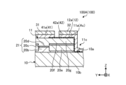
- FIG. 2 is a cross-sectional view taken along the line II--II in FIG.
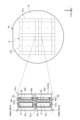
- FIG. 3 is an exemplary and schematic plan view showing a wafer on which a semiconductor element portion to be a semiconductor element according to the first embodiment is formed, and a part thereof.
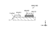
- FIG. 4 is a sectional view along IV-IV in FIG.
- FIG. 5 is an exemplary and schematic plan view of the semiconductor device of the second embodiment.
- FIG. 6 is an exemplary schematic plan view of part of the wafer of the third embodiment.
- FIG. 7 is an exemplary and schematic plan view of the semiconductor device of the fourth embodiment.
- FIG. 8 is an exemplary and schematic plan view of the semiconductor device of the fifth embodiment.
- FIG. 9 is an exemplary and schematic plan view of the semiconductor device of the sixth embodiment.
- FIG. 10 is an exemplary schematic plan view of part of the wafer of the seventh embodiment.
- 11 is an exemplary schematic plan view of section XI of FIG. 10.
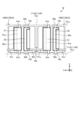
- FIG. 12 is an exemplary schematic plan view of a semiconductor element array cut out from the wafer of the seventh embodiment.
- Exemplary embodiments of the present invention are disclosed below.
- the configurations of the embodiments shown below and the actions and results (effects) brought about by the configurations are examples.
- the present invention can be realized by configurations other than those disclosed in the following embodiments.
- the X direction is indicated by the arrow X
- the Y direction is indicated by the arrow Y
- the Z direction is indicated by the arrow Z.
- the X-, Y-, and Z-directions intersect each other and are orthogonal to each other.
- the X direction is referred to as the longitudinal direction or extension direction
- the Y direction as the lateral direction or width direction
- the Z direction as the stacking direction or height direction.
- each figure is a schematic diagram for the purpose of explanation, and the scale and proportions of each figure and the actual product do not necessarily match.
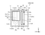
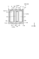
- FIG. 1 is a plan view of the semiconductor device 100A (100) of the first embodiment, and FIG. 2 is a sectional view taken along line II-II of FIG.
- the semiconductor device 100A is configured as, for example, a known semiconductor optical amplifier.
- a semiconductor device 100A includes a body 11 including a substrate 10 and a plurality of semiconductor layers, an insulating layer 12 and electrodes 31 and 32 formed on the body 11, and the electrodes 31 and 32 formed on the body 11. and conductor layers 41 and 42 electrically connected to 32 .
- the body 11 also includes a second layer 20c as an active layer extending in the X direction.
- the second layer 20c extends substantially along the X direction with a predetermined width in the Y direction and a predetermined height in the Z direction at a substantially constant position in the Z direction.
- the substrate 10 has a substantially constant thickness in the Z direction and spreads across the Z direction.
- the substrate 10 has a surface 10a and a surface 10b.
- the surface 10a faces the Z direction and intersects the Z direction.
- the surface 10b is located on the opposite side of the surface 10a, faces in the direction opposite to the Z direction, and intersects the Z direction.
- the substrate 10 is made of n-InP, for example.
- a plurality of semiconductor layers such as first to third layers 20b to 20d, current blocking layers 20e and 20f, and a clad layer 20g are laminated in the Z direction on the surface 10a of the substrate 10. ing.
- the Z direction is an example of a first direction.
- the body 11 also has a mesa 21 including the first layer 20b to the third layer 20d. As described above, the second layer 20c included in the mesa 21 is an active layer and functions as an optical waveguide.
- the body 11 has an embedded waveguide structure (BH waveguide structure).
- the first layer 20b is made of n-InP, for example, and functions as a cladding layer in the mesa 21.
- the second layer 20c has a laminated structure containing n-InGaAsP, for example, and is a so-called quaternary layer. Since the second layer 20c functions as an active layer, it has a composition that functions appropriately for light in the 1.55 [ ⁇ m] wavelength band, for example.
- the third layer 20d is made of p-InP, for example, and functions as a clad layer in the mesa 21.
- the mesa 21 is surrounded by current blocking layers 20e and 20f and a cladding layer 20g adjacent in the Z direction.
- the current blocking layer 20e is made of p-InP, for example, and the current blocking layer 20f is made of n-InP, for example.
- the clad layer 20g is made of, for example, p-InP.
- Conductor layers 41 and 42 are provided on the clad layer 20g, that is, on the side opposite to the substrate 10 with respect to the clad layer 20g.
- an electrode 31 is provided on the conductor layer 41, that is, on the side opposite to the substrate 10 with respect to the conductor layer 41, and on the conductor layer 42, that is, on the side opposite to the substrate 10 with respect to the conductor layer 42,
- An electrode 32 is provided.
- the electrodes 31 and 32 have different polarities.
- the electrode 31 is separated from the active layer in the Z direction and constitutes a P-side electrode. It can be said that the conductor layer 41 also constitutes a part of the P-side electrode.
- the end face (side surface) of the body 11 in the Y direction and the direction opposite to the Y direction and the end face 11a (upper surface) in the Z direction are covered with the insulating layer 12 except for an opening on the body 11 through which the conductor layer 41 penetrates.
- the conductor layer 41 is in contact with the end face 11a, and the electrode 31 is electrically connected to the end face 11a through the conductor layer 41.
- the insulating layer 12 is made of SiN, for example.
- the insulating layer 12 is interposed between the end surface 11 a and the conductor layer 42 and the electrode 32 .
- the conductor layer 42 and the electrode 32 are insulated from the end surface 11a.
- the conductor layer 42 is separated from the conductor layer 41 in the Y direction and extends to the side and bottom surfaces of the recess 11c provided on the body 11 .
- An opening is provided in the insulating layer 12 at the bottom surface of the recess 11c, and the conductor layer 42 is electrically connected to the substrate 10 in the opening.
- a current can be passed through a plurality of semiconductor layers.
- the semiconductor device 100 is configured as an optical semiconductor device such as a semiconductor optical amplifier, the current can activate the second layer 20c.
- the body 11 has a quadrangular shape in plan view when viewed in the direction opposite to the Z direction.
- the body 11 has edges 11d1, 11d2, 11d3, and 11d4 forming the periphery in plan view.
- the edge 11d1 extends along the Y direction at the end in the X direction.
- the edge 11d2 extends along the Y direction at the end opposite to the X direction.
- the edge 11d3 extends along the X direction at the end in the Y direction.
- the edge 11d4 extends along the X direction at the end opposite to the Y direction.
- Edges 11d1 and 11d2 are examples of first edges
- edges 11d3 and 11d4 are examples of second edges.
- the X direction is an example of the second direction
- the Y direction is an example of the third direction.
- the end face 11a is covered with an insulating layer 12.
- the insulating layer 12 has a covering portion 12a covering the end surface 11a except for the openings through which the conductor layers 41 and 42 pass.
- the peripheral portion of the covering portion 12a is separated from the edges 11d1, 11d2, 11d3 and 11d4.
- the end face 11a has a covered area Ac covered with the covering part 12a and an unformed area Ae where the covering part 12a (insulating layer 12) is not formed along the edges 11d1, 11d2, 11d3, and 11d4. ing.
- the non-formation area Ae extends with a substantially constant width along the edges 11d1, 11d2, 11d3, and 11d4, but the width may not be constant.
- the non-formation area Ae may also be referred to as an exposed area.
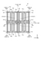
- FIG. 3 is a plan view showing the wafer W and a portion of the wafer W in an enlarged manner.
- a plurality of semiconductor element portions S arranged in a matrix are collectively formed on a substrate 10 of a wafer W by a semiconductor process.
- the semiconductor element 100A (100) is obtained by cutting along the cutting line CLx extending in the Y direction and the cutting line CLy extending in the Y direction. That is, the semiconductor element section S has substantially the same configuration as the semiconductor element 100 .
- Cutting line CLx forms edges 11d1 and 11d2 in semiconductor element 100
- cutting line CLy forms edges 11d3 and 11d4 in semiconductor element 100.
- FIG. Note that the cutting lines CLx and CLy may also be referred to as planned cutting lines or imaginary boundary lines.
- the presence of the insulating layer 12 makes it difficult to cut the wafer W along the cutting lines CLx and CLy.
- the edges 11d1, 11d2, 11d3, and 11d4 of the cut semiconductor element 100A may be roughened and uneven. Therefore, in the present embodiment, on the end face 11a of the wafer W, along the cutting lines CLx and CLy, a band-shaped region Ae in which the insulating layer 12 is not formed is provided centering on the cutting lines CLx and CLy. ing.
- the cutting along the cutting lines CLx and CLy it is possible to avoid the occurrence of an undesirable event due to the insulating layer 12 .
- the electrodes 31 and 32 are formed in a state in which the semiconductor element portion S is integrated with the wafer W, like other components of the semiconductor element 100A (100).
- the electrodes 31 and 32 are formed to have a predetermined shape at predetermined positions on the conductor layers 41 and 42 provided in each semiconductor element portion S by an electrolytic plating method.
- the electrodes 31 and 32 are formed by electrolytic plating, if the potential difference between the plurality of conductor layers 41 or the plurality of conductor layers 42 on the wafer W is large, the thickness of the electrodes 31 and 32 in the Z direction.
- variations may occur. Such variations in the shape of the electrodes 31 and 32 may contribute to variations in the performance of the semiconductor device 100 (individual differences).
- wiring portions 41b and 42b are provided on the conductor layers 41 and 42 of each semiconductor element portion S (semiconductor element 100).
- the wiring portion 41b electrically connects a plurality of covering portions 41a adjacent to each other on the wafer W in the X direction.
- the wiring portion 42b electrically connects the plurality of covering portions 42a adjacent to each other on the wafer W in the X direction.
- the potential difference between the plurality of conductor layers 41 and between the plurality of conductor layers 42 between the plurality of semiconductor element portions S can be made smaller.
- wiring portion 41b extends between electrode 31 and edge 11d1 or edge 11d2
- wiring portion 42b extends between electrode 32 and edge 11d1 or edge 11d2.
- the wiring portions 41b and 42b are examples of wiring.
- the insulating layer 12 is not provided in the non-formation regions Ae along the cutting lines CLx and CLy, whereas the wiring portions 41b and 42b are provided across the cutting lines CLy. I'm in.
- both of the wiring portions 41b and 42b electrically connected to the electrodes 31 and 32 having different polarities are in contact with the non-formation region Ae of the end surface 11a, the wiring portions 41b and 42b A short circuit of current may occur between them.
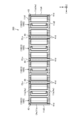
- FIG. 4 is a sectional view along IV-IV in FIG.
- one of the wiring portions 41b and 42b which corresponds to the wiring portion 42b in this embodiment as an example, is connected to the wiring portion 42b and the end surface 11a.
- An intervening portion 12b intervening between is provided. As shown in FIG.
- the intervening portion 12b extends forward in the X direction and rearward in the X direction from the covering portion 12a of the insulating layer 12 at the position where the wiring portion 42b is provided, and the non-formation region Ae. are divided.
- the intervening portion 12b is interposed between the wiring portion 42b and the end face 11a at a position shifted from the non-formation region Ae.
- the wiring part 41b is provided on the non-formation region Ae, and is an example of the first wiring.
- the wiring portion 42b is provided on the intervening portion 12b and is an example of a second wiring.
- the electrode 31 is an example of a first electrode
- the electrode 32 is an example of a second electrode.
- the intervening portion 12b as the insulating layer 12 is provided at the position where the wiring portion 42b is provided.
- the section in which the intervening portion 12b is provided is relatively short, and the insulating layer 12 is not provided in other sections of the cutting lines CLx and CLy. In the cutting of the insulating layer 12 as described above, the inconvenience caused by the insulating layer 12 can be avoided.
- the present embodiment by providing the non-formation regions Ae of the insulating layer 12 along the cutting lines CLx and CLy, the occurrence of an inconvenient event due to the insulating layer 12 during cutting of the wafer W can be prevented.
- the wiring portions 41b and 42b while avoiding this, variations in the electrodes 31 and 32 formed on the wafer W by the electroplating method can be suppressed.
- the electrode 31 in the semiconductor element 100 can be prevented from being caused by the insulating layer 12 when the wafer W is cut. , 32 can be prevented from short-circuiting between the wiring portions 41b and 42b.
- the wiring portion 42b (the conductor layer 42) is electrically connected to the substrate 10 in this embodiment.
- the intervening portion 12b is provided between the wiring portion 42b electrically connected to the substrate 10 and the non-formation region Ae, so that the non-uniformity between the end surface 11a and the substrate 10 is eliminated. Intentional short circuit of current can be prevented.
- a semiconductor element array (not shown) can be obtained by cutting out a plurality of semiconductor element portions S adjacent in the Y direction from the wafer W in an integrated state.
- Such a configuration is suitable, for example, for application to optical devices having a plurality of semiconductor optical amplifiers, such as optical matrix switches.
- FIG. 5 is a plan view of the semiconductor device 100B (100) of the second embodiment.
- intervening portions 12b are provided not only between the wiring portion 42b and the end face 11a, but also between the wiring portion 41b and the end face 11a.
- the insulating layer 12 may be provided at a position separate from the intervening portion 12b as long as it is within a range where occurrence of an undesirable event due to the insulating layer 12 during the cutting of the wafer W can be avoided.
- the length along the edges 11d1 to 11d4 of the non-formation area Ae may be shorter.
- FIG. 6 is a plan view of the wafer W of the third embodiment. As shown in FIG. 6, the wafer W of this embodiment is provided with wiring portions 41c and 42c in addition to the wiring portions 41b and 42b similar to those of the above embodiment.
- the wiring portions 41c and 42c electrically connect the electrodes 31 and 32 adjacent to each other in the Y direction in the two semiconductor element portions S adjacent to each other in the Y direction.
- the wiring portion 41c extends in the Y direction from the covering portion 41a of the conductor layer 41 to the cutting line CLx
- the wiring portion 42c extends in the opposite direction of the Y direction from the covering portion 42a of the conductor layer 42 to the cutting line CLx. ing.
- the end of the wiring portion 41c and the end of the wiring portion 42c at the cutting line CLx face each other and are electrically connected to each other.
- the end of the wiring portion 41c at the edge 11d3 and the end of the wiring portion 42c at the edge 11d4 are aligned in the Y direction.
- the wiring portions 41b, 42b, 41c, and 42c electrically connect more covering portions 41a and 42a, and these covering portions 41a and 42a are electrically connected.
- the potential difference between them can be made smaller. Therefore, according to the present embodiment, it is possible to further suppress variations in the specifications of the electrodes 31 and 32 among the plurality of semiconductor elements 100 and, in turn, variations in the performance of the semiconductor elements 100 .
- the wiring portions 41c and 42c are both provided on the intervening portion 12b and are an example of the second wiring.
- FIG. 7 is a plan view of the semiconductor device 100D (100) of the fourth embodiment.
- the semiconductor device 100D of this embodiment has a U-shaped waveguide including two second layers 20c and one passive portion 20u arranged at approximately the same position in the Z direction. have.
- the two second layers 20c both extend in the X direction and are arranged substantially parallel to each other with a gap in the Y direction.
- the passive part 20u is curved in a convex shape in the direction opposite to the X direction, and connects the ends of the two second layers 20c in the direction opposite to the X direction.
- the semiconductor element 100D of this embodiment also has the non-formation region Ae, the wiring portions 41b and 42b, and the intervening portion 12b, similar to the first embodiment. Therefore, this embodiment can also provide the same effects as the first embodiment.
- FIG. 8 is a plan view of the semiconductor device 100E (100) of the fifth embodiment.
- the semiconductor element 100E of this embodiment has two second layers 20c, and has the same configuration as in FIGS. 1 and 2 corresponding to each of the second layers 20c. ing.
- the semiconductor device 100E has two sets of configurations similar to those of the first embodiment.
- the two second layers 20c can be operated independently.
- the semiconductor element 100E of the present embodiment also has the non-formation region Ae, the wiring portions 41b and 42b, and the intervening portion 12b as in the first embodiment. Therefore, this embodiment can also provide the same effects as the first embodiment.
- the semiconductor element 100 having the second layer 20c and three or more sets of structures corresponding to the second layer 20c also has the non-formation region Ae, the wiring portions 41b and 42b, and the intervening portions, similarly to the first embodiment. 12b, the same effects as those of the first embodiment can be obtained.
- FIG. 9 is a plan view of the semiconductor element 100F (100) of the sixth embodiment.
- the semiconductor element 100F of this embodiment also has two second layers 20c, like the fifth embodiment.
- the electrode 32 is shared for the actuation of the two second layers 20c. Therefore, the semiconductor element 100F has two electrodes 31 and one electrode 31 .
- the semiconductor element 100E of the present embodiment also has the non-formation region Ae, the wiring portions 41b and 42b, and the intervening portion 12b as in the first embodiment. Therefore, this embodiment can also provide the same effects as the first embodiment.
- FIG. 10 is a plan view of the wafer W of the seventh embodiment. Moreover, FIG. 11 is an enlarged view of the XI section of FIG.
- a plurality of semiconductor element portions S-1 to S-4 (semiconductor elements 100G) formed on the wafer W have substantially the same configuration as the semiconductor element 100F of the sixth embodiment. ing.
- the wafer W of this embodiment is provided with wiring portions 41d and 43 in addition to the wiring portions 41b and 42b similar to those of the above embodiment.
- the wiring portions 41d and 43 electrically connect the electrodes 31G (31) adjacent to each other in the Y direction in the two semiconductor element portions S-1 and S-2 adjacent to each other in the Y direction.
- the wiring portions 41d and 43 pass through the four semiconductor element portions S-1 to S-4.
- the wiring portions 41d provided in the semiconductor element portions S-1 and S-2 extend from the electrode 31 in the opposite direction of the X direction to the cutting line CLy (edge 11d2). extends to
- the wiring portions 43 provided in the semiconductor element portions S-3 and S-4 each have an L-shape, and are separated by a cutting line CLy (edge 11d1) and a cutting line CLx (edge 11d3 or edge 11d4). extends between In the wafer W, the end portion 41d1 of the wiring portion 41d and the end portion 43a of the wiring portion 43 at the cutting line CLy face each other and are electrically connected to each other.
- the ends 43b of the two wiring portions 43 on the cutting line CLx face each other and are electrically connected to each other. Therefore, in the semiconductor element 100G cut out from the wafer W, the end portion 43a of the wiring portion 43 at the edge 11d1 and the end portion 41d1 of the wiring portion 41d at the edge 11d2 are aligned in the X direction, and the wiring portion at the edge 11d3. 43 and the end 43b of the wiring portion 43 at the edge 11d4 are arranged in the Y direction.
- more covering portions 41a and 42a are electrically connected by wiring portions 41b, 42b, 41d, and 43 in electrolytic plating for forming electrodes 31 and 32, as in the third embodiment.
- the potential difference between the covering portions 41a and 42a can be further reduced. Therefore, according to the present embodiment, it is possible to further suppress variations in the specifications of the electrodes 31 and 32 among the plurality of semiconductor elements 100 and, in turn, variations in the performance of the semiconductor elements 100 .
- FIG. 12 is a plan view of a semiconductor element array 200 integrally having a plurality of semiconductor element portions S of this embodiment arranged in the Y direction.
- the semiconductor element array 200 has wiring portions 41b, 42b, 41d, 43, and a wiring portion 44 integrally having wiring portions 43 adjacent to each other in the Y direction.
- the wiring portions 41b, 42b, 41d extend between the electrode 31 or the electrode 32 and the edge 11d1 or the edge 11d2.
- the wiring portions 43 and 44 are not connected to any of the electrodes 31 and 32, have a U-shaped or L-shaped shape, and extend between the edge 11d1 and the edge 11d1 or the edges 11d3 and 11d4.
- the electrodes 31 and 32 adjacent to each other in the Y direction are formed. However, they cannot be used because they are electrically connected through the wiring portions 41c and 42c and short-circuited. This is because the wiring portions 41c and 42c electrically connecting the electrodes 31 and 32 on the wafer W pass through only the cutting lines CLx which are not cut when forming the semiconductor element array.
- the wiring portions 41d, 43, 44 extending between the electrodes 31, 32 adjacent in the Y direction are cut when forming the semiconductor element array 200, as shown in FIG. Since the electrodes 31 and 32 are separated at the cutting line CLy, the semiconductor element array 200 in which the electrodes 31 and 32 are not short-circuited by the wiring portions 41d, 43 and 44 can be obtained.
- the semiconductor element portion S (semiconductor element 100G) of the present embodiment includes wiring portions 41b, 42b, 41d, but does not have wiring portions extending between the electrodes 31, 32 and the edges 11d3, 11d4.
- the semiconductor element 100G also has a wiring portion 43 electrically insulated from the electrodes 31 and 32 and extending between the edge 11d1 and the edge 11d3 or the edge 11d4.
- the wiring portion 43 is an example of a third wiring.
- the semiconductor element array 200 of this embodiment also has a U-shaped wiring portion 44 extending between two ends 43a (see FIG. 11) that are separated in the Y direction facing the edge 11d1 (see FIG. 12). reference).
- the wiring portion 44 is substantially aligned in the X direction with the two wiring portions 41d facing the edge 11d2.
- the wiring portion 44 is an example of a fourth wiring.
- the optical semiconductor element can be applied to a laser emitting element such as a DFB semiconductor laser, or a semiconductor element other than an optical semiconductor element.
- the present invention can be used for semiconductor devices, semiconductor device arrays, and wafers.
- SYMBOLS 10 Substrate 10a... Surface 10b... Surface 11... Body 11a... End surface 11c... Recessed part 11d1, 11d2... Edge (first edge) 11d3, 11d4... Edge (second edge) DESCRIPTION OF SYMBOLS 12... Insulating layer 12a... Covering part 12b... Interposed part 20b... First layer (semiconductor layer) 20c... Second layer (semiconductor layer) 20d... Third layer (semiconductor layer) 20e... Current blocking layer (semiconductor layer) 20f... Current blocking layer (semiconductor layer) 20g...
- Wiring portion (wiring, fourth wiring) 100, 100A to 100G Semiconductor element 200 Semiconductor element array Ac Covered area Ae Non-formation area CLx, CLy Cutting line S, S-1 to S-4 Semiconductor element part W Wafer X Direction (second direction) Y... direction (third direction) Z direction (first direction)
Landscapes
- Physics & Mathematics (AREA)
- Condensed Matter Physics & Semiconductors (AREA)
- General Physics & Mathematics (AREA)
- Electromagnetism (AREA)
- Optics & Photonics (AREA)
- Geometry (AREA)
- Internal Circuitry In Semiconductor Integrated Circuit Devices (AREA)
- Semiconductor Lasers (AREA)
Abstract
半導体素子は、例えば、基板と、当該基板上に第一方向に積層された複数の半導体層と、第一方向の端面と、第一方向の反対方向に見た場合における周縁を構成するエッジと、を含むボディと、端面を覆う絶縁層と、端面に対して基板とは反対側に設けられた電極と、電極と電気的に接続されるとともに当該電極とエッジとの間で延びた少なくとも一つの配線と、を備え、端面には、エッジに沿って絶縁層の不形成領域が設けられ、絶縁層は、不形成領域とずれた位置で端面と配線との間に介在した介在部位を有する。
Description
本発明は、半導体素子、半導体素子アレイ、およびウエハに関する。
従来、ウエハ上に半導体層や導体層等を積層して複数の光半導体素子部を形成し、当該複数の光半導体素子部をウエハから切り出すことにより、複数の光半導体素子を製造する技術が、知られている(例えば、特許文献1)。
特許文献1では、ウエハ上で隣接する電極間が配線(導通線)によって電気的に接続されている。これにより、光半導体素子の製造工程において当該光半導体素子のそれぞれに設けられる電極を電解メッキによって形成する際に、各部の電位差によって電極の厚さのばらつき(個体差)が生じるのが抑制されている。半導体層の上面と配線との間には、誘電体層のような絶縁層が設けられている。
しかしながら、絶縁層がウエハ上で複数の光半導体素子部の境界を跨ぐように設けられていると、当該絶縁層が障害となり、例えば、光半導体素子部がウエハから切り出され難くなったり、活性層を含む光半導体素子の切断された端面が荒れやすくなったりするなど、不都合な事象が生じる虞があった。また、これと同様の不都合な事象は、光半導体素子ではない半導体素子でも起こりうる。
そこで、本発明の課題の一つは、例えば、ウエハからの複数の半導体素子部の切り出しを、より容易に、より確実に、あるいはより精度良く実行することが可能となるような、新規な改善された半導体素子、半導体素子アレイ、およびウエハを得ること、である。
本発明の半導体素子は、例えば、基板と、当該基板上に第一方向に積層された複数の半導体層と、前記第一方向の端面と、前記第一方向の反対方向に見た場合における周縁を構成するエッジと、を含むボディと、前記端面を覆う絶縁層と、前記端面に対して前記基板とは反対側に設けられた電極と、前記電極と電気的に接続されるとともに当該電極と前記エッジとの間で延びた少なくとも一つの配線と、を備え、前記端面には、前記エッジに沿って前記絶縁層の不形成領域が設けられ、前記絶縁層は、前記不形成領域とずれた位置で前記端面と前記配線との間に介在した介在部位を有する。
前記半導体素子は、前記半導体層としての活性層と、当該活性層に対して電流を供給する前記電極とを備えた、光半導体素子として構成されてもよい。
前記半導体素子は、前記配線として複数の配線を備え、前記配線は、前記不形成領域上に設けられた第一配線と、前記介在部位上に設けられた第二配線と、を含んでもよい。
前記半導体素子は、前記電極として互いに極性の異なる第一電極と第二電極とを備え、前記第一配線は、前記第一電極と電気的に接続され、前記第二配線は、前記第二電極と電気的に接続されてもよい。
前記半導体素子では、前記第二電極は、前記基板と電気的に接続されてもよい。
前記半導体素子は、前記エッジとして、前記第一方向と交差した第二方向の前方および後方に位置した第一エッジと、前記第一方向および前記第二方向と交差した第三方向の前方および後方に位置した第二エッジと、を備え、前記配線として、前記電極と前記第一エッジとの間で延びた配線を備えるとともに、前記電極と前記第二エッジとの間で延びた配線を備えなくてもよい。
前記半導体素子は、前記電極とは電気的に接続されず、前記第一エッジと前記第二エッジとの間で延びた第三配線を備えてもよい。
本発明の半導体素子は、例えば、基板と、当該基板上に第一方向に積層された複数の半導体層と、前記第一方向の端面と、前記第一方向の反対方向に見た場合における周縁を構成するエッジと、を含むボディと、前記端面を覆う絶縁層と、前記端面の上に設けられた電極と、前記電極と電気的に接続されるとともに当該電極と前記エッジとの間で延びた少なくとも一つの配線と、を備え、前記端面には、前記エッジに沿った前記絶縁層の不形成領域が設けられ、前記エッジとして、前記第一方向と交差した第二方向の前方および後方に位置した第一エッジと、前記第一方向および前記第二方向と交差した第三方向の前方および後方に位置した第二エッジと、を備え、前記配線として、前記電極と前記第一エッジとの間で延びた配線を備えるとともに、前記電極と前記第二エッジとの間で延びた配線を備えない。
本発明の半導体素子アレイは、例えば、基板と、当該基板上に第一方向に積層された複数の半導体層と、前記第一方向の端面と、前記第一方向の反対方向に見た場合に前記第一方向と交差した第二方向の前方および後方に位置した第一エッジと、を含むボディと、前記端面を覆う絶縁層と、前記端面上に設けられた複数の電極と、前記電極と電気的に接続されるとともに当該電極と前記第一エッジとの間で延びた少なくとも一つの配線と、を備え、前記第一方向および前記第二方向と交差した第三方向に並ぶ複数の半導体素子部が構成された、半導体素子アレイであって、前記端面には、前記第一方向の反対方向に見た場合に、前記第一エッジに沿って絶縁層の不形成領域が設けられるとともに、前記絶縁層は、前記不形成領域とずれた位置で前記端面と前記配線との間に介在した介在部位を有する。
前記半導体素子アレイでは、前記複数の半導体素子部は、略同一の構成を有してもよい。
前記半導体素子アレイは、前記配線としての二つの第一配線であって、前記第二方向に互いに隣接した電極のそれぞれと、前記第二方向の前方および後方のうち一方の前記第一エッジと、の間で延び、前記第三方向に間隔をあけて並んだ二つの第一配線と、前記第二方向の前方および後方のうちの他方の第一エッジに位置するとともに互いに第三方向間隔をあけて並んだ二つの端部を有し、当該他方の第一エッジから離れた位置を経由して前記二つの端部間で延び、前記二つの第一配線と前記第二方向に並んだ第四配線と、を備えてもよい。
前記半導体素子アレイでは、前記半導体素子部は、それぞれ、前記半導体層としての活性層と当該活性層に対して電流を供給する前記電極とを有した光半導体素子部として構成されてもよい。
本発明のウエハは、例えば、基板と、前記基板上に第一方向に積層された複数の半導体層と、前記第一方向の端面と、前記第一方向と交差した第二方向および前記第一方向および前記第二方向と交差した第三方向にマトリクス状に並んだ複数の半導体素子部を備えたウエハであって、当該ウエハから切り出した半導体素子部が、上記半導体素子、または請上記半導体素子アレイとなるよう構成されたウエハであって、前記電極としての複数の電極が前記配線を介して電気的に接続される。
前記ウエハでは、前記半導体素子部は、それぞれ、前記半導体層としての活性層と当該活性層に対して電流を供給する前記電極とを有した光半導体素子部として構成されてもよい。
本発明によれば、新規な改善された半導体素子、半導体素子アレイ、およびウエハを得ることができる。
以下、本発明の例示的な実施形態が開示される。以下に示される実施形態の構成、ならびに当該構成によってもたらされる作用および結果(効果)は、一例である。本発明は、以下の実施形態に開示される構成以外によっても実現可能である。また、本発明によれば、構成によって得られる種々の効果(派生的な効果も含む)のうち少なくとも一つを得ることが可能である。
以下に示される複数の実施形態は、同様の構成を備えている。よって、各実施形態の構成によれば、当該同様の構成に基づく同様の作用および効果が得られる。また、以下では、それら同様の構成には同様の符号が付与されるとともに、重複する説明が省略される場合がある。
本明細書において、序数は、方向や、部材、部位等を区別するために便宜上付与されており、優先順位や順番を示すものではない。
各図において、X方向を矢印Xで表し、Y方向を矢印Yで表し、Z方向を矢印Zで表す。X方向、Y方向、およびZ方向は、互いに交差するとともに互いに直交している。また、以下では、X方向を長手方向若しくは延び方向、Y方向を短手方向若しくは幅方向、Z方向を積層方向若しくは高さ方向と称する。
また、各図は説明を目的とした模式図であって、各図と実物とでスケールや比率は、必ずしも一致しない。
[第1実施形態]
図1は、第1実施形態の半導体素子100A(100)の平面図であり、図2は、図1のII-II断面図である。半導体素子100Aは、例えば、公知の半導体光増幅器として構成される。
図1は、第1実施形態の半導体素子100A(100)の平面図であり、図2は、図1のII-II断面図である。半導体素子100Aは、例えば、公知の半導体光増幅器として構成される。
図1,2に示されるように、半導体素子100Aは、基板10と複数の半導体層とを含むボディ11と、ボディ11上に形成された絶縁層12および電極31,32と、当該電極31,32と電気的に接続された導体層41,42と、を備えている。
また、ボディ11内には、X方向に延びた活性層としての第二層20cが含まれている。第二層20cは、Z方向における略一定の位置において、Y方向における所定幅およびZ方向における所定高さで、X方向に略沿って延びている。
図2に示されるように、基板10は、Z方向に略一定の厚さを有し、Z方向と交差して広がっている。図2に示されるように、基板10は、面10aと、面10bと、を有している。面10aは、Z方向を向くとともに、Z方向と交差している。また、面10bは、面10aとは反対側に位置し、Z方向の反対方向を向くとともに、Z方向と交差している。基板10は、例えば、n-InPで作られている。
ボディ11において、基板10の面10a上には、例えば、第一層20b~第三層20d、電流阻止層20e,20f、およびクラッド層20gのような複数の半導体層が、Z方向に積層されている。Z方向は第一方向の一例である。
また、ボディ11は、第一層20b~第三層20dを含むメサ21を有している。上述したように、メサ21に含まれる第二層20cは活性層であり、光導波路として機能する。ボディ11は、埋め込み導波路構造(BH導波路構造)を有している。
第一層20bは、例えば、n-InPで作られており、メサ21においては、クラッド層として機能する。
第二層20cは、例えば、n-InGaAsPを含んだ積層構造を有しており、所謂四元層である。第二層20cは、活性層として機能するため、例えば、波長1.55[μm]帯の光に対して適切に機能する組成を有している。
第三層20dは、例えば、p-InPで作られており、メサ21において、クラッド層として機能する。
ボディ11内で、メサ21は、電流阻止層20e,20f、ならびにZ方向に隣接したクラッド層20gによって囲まれている。電流阻止層20eは、例えば、p-InPで作られ、電流阻止層20fは、例えば、n-InPで作られている。また、クラッド層20gは、例えば、p-InPで作られている。
クラッド層20g上、すなわちクラッド層20gに対して基板10とは反対側には、導体層41,42が設けられている。また、導体層41上、すなわち導体層41に対して基板10とは反対側には、電極31が設けられ、導体層42上、すなわち導体層42に対して基板10とは反対側には、電極32が設けられている。電極31,32は、互いに極性が異なる。
電極31は、活性層に対してZ方向に離間し、P側電極を構成している。なお、導体層41も、P側電極の一部を構成していると言うことができる。
ボディ11のY方向およびY方向の反対方向の端面(側面)、ならびにZ方向の端面11a(上面)は、ボディ11上で導体層41が貫通する開口部を除き、絶縁層12で覆われている。言い換えると、導体層41は、端面11aと接しており、電極31は、導体層41を介して端面11aと電気的に接続されている。なお、絶縁層12は、例えば、SiNで作られる。
また、端面11aと導体層42および電極32との間には、絶縁層12が介在している。言い換えると、導体層42および電極32は、端面11aとは絶縁されている。また、導体層42は、Y方向において、導体層41とは、離間するとともに、ボディ11上に設けられた凹部11cの側面および底面まで延びている。凹部11cの底面において、絶縁層12には開口が設けられており、当該開口において、導体層42は、基板10と電気的に接続されている。
電極31,32間に電圧を印加することにより、複数の半導体層に電流を流すことができる。半導体素子100が、半導体光増幅器のような光半導体素子として構成されている場合、当該電流によって第二層20cを活性化することができる。
図1に示されるように、ボディ11は、Z方向の反対方向に見た場合の平面視において、四角形状の形状を有している。ボディ11は、当該平面視における周縁を形成するエッジ11d1,11d2,11d3,11d4を有している。エッジ11d1は、X方向の端部において、Y方向に沿って延びている。エッジ11d2は、X方向の反対方向の端部において、Y方向に沿って延びている。エッジ11d3は、Y方向の端部において、X方向に沿って延びている。また、エッジ11d4は、Y方向の反対方向の端部において、X方向に沿って延びている。エッジ11d1,11d2は、第一エッジの一例であり、エッジ11d3,11d4は、第二エッジの一例である。また、X方向は、第二方向の一例であり、Y方向は、第三方向の一例である。
また、端面11aは、絶縁層12で覆われている。絶縁層12は、上述した導体層41,42が貫通する開口部を除き端面11a上を覆う被覆部12aを有している。被覆部12aの周縁部は、エッジ11d1,11d2,11d3,11d4から離間している。言い換えると、端面11aは、被覆部12aによって覆われた被覆領域Acと、エッジ11d1,11d2,11d3,11d4に沿って被覆部12a(絶縁層12)が形成されない不形成領域Aeと、を有している。不形成領域Aeは、エッジ11d1,11d2,11d3,11d4に沿って略一定幅で延びているが、幅は一定でなくてもよい。不形成領域Aeは、露出領域とも称されうる。
図3は、ウエハWおよび当該ウエハW上の一部を拡大して示す平面図である。図3に示されるようにウエハWの基板10上に、半導体プロセスによって、マトリクス状に配置された複数の半導体素子部Sが一括して形成され、その後、当該ウエハWから半導体素子部SがX方向に延びた切断線CLxおよびY方向に延びた切断線CLyで切り出されることにより、半導体素子100A(100)が得られる。すなわち、半導体素子部Sは、半導体素子100と略同じ構成を有している。切断線CLxは、半導体素子100においてエッジ11d1,11d2となり、切断線CLyは、半導体素子100においてエッジ11d3,11d4となる。なお、切断線CLx,CLyは、切断予定線や、仮想境界線とも称されうる。
ここで、仮に、切断線CLx,CLy上が絶縁層12で覆われていると、当該絶縁層12が存在している分、例えば、ウエハWを切断線CLx,CLyに沿って切断し難くなったり、切り出された半導体素子100Aの切断された端面としてのエッジ11d1,11d2,11d3,11d4が荒れて凹凸が生じたり、といった不都合な事象が生じる虞がある。このため、本実施形態では、ウエハWの端面11a上には、切断線CLx,CLyに沿って、当該切断線CLx,CLyを中心とした帯状に、絶縁層12の不形成領域Aeが設けられている。これにより、切断線CLx,CLyでの切断において、絶縁層12による不都合な事象が生じるのを、回避することができる。
また、電極31,32は、半導体素子100A(100)の他の構成要素と同様に、半導体素子部SがウエハWに一体化されている状態で形成される。電極31,32は、電解メッキ法によって、各半導体素子部Sに設けられた導体層41,42上の所定位置に、所定形状となるように形成される。ここで、電解メッキ法によって電極31,32を形成する際に、ウエハW上の複数の導体層41間または複数の導体層42間での電位差が大きいと、電極31,32のZ方向の厚さ等に、ばらつき(個体差)が生じる虞がある。このような電極31,32の形状のばらつきは、半導体素子100の性能のばらつき(個体差)の一因となる虞がある。
そこで、本実施形態では、図3に示されるように、各半導体素子部S(半導体素子100)の導体層41,42に、配線部41b,42bを設けている。配線部41bは、ウエハW上でX方向に隣接した複数の被覆部41a間を電気的に接続している。また、配線部42bは、ウエハW上でX方向に隣接した複数の被覆部42a間を電気的に接続している。これにより、ウエハW上では、X方向に並ぶ複数の半導体素子部Sの列において、複数の被覆部41aが配線部41bを介して互いに電気的に接続されるとともに、複数の被覆部42aが配線部42bを介して互いに電気的に接続されることになる。よって、本実施形態によれば、電極31,32を形成する電解メッキにおいて、複数の半導体素子部S間で複数の導体層41間、および複数の導体層42間での電位差をより小さくすることができ、これにより複数の半導体素子100間で、電極31,32のスペックのばらつき、ひいては半導体素子100の性能のばらつきが生じるのを、抑制することができる。なお、半導体素子100において、配線部41bは、電極31とエッジ11d1またはエッジ11d2との間で延びており、配線部42bは、電極32とエッジ11d1またはエッジ11d2との間で延びている。配線部41b,42bは、配線の一例である。
また、上述したように、ウエハWにおいて、絶縁層12は、切断線CLx,CLyに沿った不形成領域Aeには設けられていないのに対し、配線部41b,42bは、切断線CLyを跨いでいる。ここで、仮に、互いに極性が異なる電極31,32のそれぞれと電気的に接続されている配線部41b,42bの双方が、端面11aの不形成領域Aeと接していたとすると、配線部41b,42b間で電流の短絡が生じる虞がある。
そこで、本実施形態の半導体素子部S(半導体素子100)には、絶縁層12の不形成領域Aeを介した配線部41b,42b間での電流の短絡を防止するための構成が、設けられている。図4は、図1のIV-IV断面図である。図4に示されるように、本実施形態では、不形成領域Aeにおいて、配線部41b,42bのうち一方、本実施形態では一例として配線部42bに対応して、当該配線部42bと端面11aとの間に介在した介在部位12bが設けられている。図1に示されるように、介在部位12bは、配線部42bが設けられた位置において、絶縁層12の被覆部12aから、X方向の前方およびX方向の後方に延びており、不形成領域Aeを分断している。言い換えると、介在部位12bは、不形成領域Aeとずれた位置において、配線部42bと端面11aとの間に介在している。なお、配線部41bは、不形成領域Ae上に設けられており、第一配線の一例である。配線部42bは、介在部位12b上に設けられており、第二配線の一例である。また、電極31は、第一電極の一例であり、電極32は、第二電極の一例である。
上述したように、本実施形態では、配線部42bが設けられた位置については、絶縁層12としての介在部位12bが設けられることになる。しかしながら、切断線CLx,CLyのうち、当該介在部位12bが設けられる区間は比較的短く、切断線CLx,CLyの他の区間については絶縁層12が設けられていないため、切断線CLx,CLyでの切断において、上述したような絶縁層12による不都合な事象を回避することができる。
以上説明したように、本実施形態によれば、切断線CLx,CLyに沿って絶縁層12の不形成領域Aeを設けることにより、ウエハWの切断において絶縁層12による不都合な事象が生じるのを回避しながら、配線部41b,42bを設けることにより、ウエハWにおいて電解メッキ法によって形成する電極31,32のばらつきを抑制することができる。さらに、配線部42bに対応して絶縁層12として介在部位12bを部分的に設けることにより、ウエハWの切断において絶縁層12による不都合な事象が生じるのを回避しながら、半導体素子100において電極31,32のばらつきの抑制のために設けた配線部41b,42b間での電流の短絡を防止することができる、という効果が得られる。
また、上述したように、本実施形態では、配線部42b(導体層42)は、基板10と電気的に接続されている。このような構成において、仮に、配線部42bが端面11aの不形成領域Aeと接すると、端面11aと基板10との間で、導体層42を介して、第二層20cを含む半導体層を迂回した不本意な電流の短絡が生じる。この点、本実施形態によれば、基板10と電気的に接続された配線部42bと不形成領域Aeとの間に介在部位12bが設けられることにより、端面11aと基板10との間の不本意な電流の短絡を防止することができる。
また、Y方向に隣接した複数の半導体素子部Sを、それらが一体化された状態でウエハWから切り出すことにより、半導体素子アレイ(不図示)を得ることができる。このような構成は、例えば、光マトリクススイッチのような、複数の半導体光増幅器を有する光学素子への適用に、適している。
[第2実施形態]
図5は、第2実施形態の半導体素子100B(100)の平面図である。図5に示されるように、本実施形態では、配線部42bと端面11aとの間のみならず、配線部41bと端面11aとの間にも、介在部位12bが設けられている。本実施形態によっても、上記第1実施形態と同様の効果が得られる。なお、ウエハWの切断において絶縁層12による不都合な事象が生じるのを回避できる範囲内であれば、介在部位12bとは外れた位置に設けられてもよい。言い換えると、不形成領域Aeのエッジ11d1~11d4に沿う長さは、より短くてもよい。
図5は、第2実施形態の半導体素子100B(100)の平面図である。図5に示されるように、本実施形態では、配線部42bと端面11aとの間のみならず、配線部41bと端面11aとの間にも、介在部位12bが設けられている。本実施形態によっても、上記第1実施形態と同様の効果が得られる。なお、ウエハWの切断において絶縁層12による不都合な事象が生じるのを回避できる範囲内であれば、介在部位12bとは外れた位置に設けられてもよい。言い換えると、不形成領域Aeのエッジ11d1~11d4に沿う長さは、より短くてもよい。
[第3実施形態]
図6は、第3実施形態のウエハWの平面図である。図6に示されるように、本実施形態のウエハWには、上記実施形態と同様の配線部41b,42bに加えて、配線部41c,42cが設けられている。配線部41c,42cは、Y方向に互いに隣接した二つの半導体素子部SにおいてY方向に互いに隣接した電極31,32間を、電気的に接続している。
図6は、第3実施形態のウエハWの平面図である。図6に示されるように、本実施形態のウエハWには、上記実施形態と同様の配線部41b,42bに加えて、配線部41c,42cが設けられている。配線部41c,42cは、Y方向に互いに隣接した二つの半導体素子部SにおいてY方向に互いに隣接した電極31,32間を、電気的に接続している。
具体的に、配線部41cは、導体層41の被覆部41aから切断線CLxまでY方向に延び、配線部42cは、導体層42の被覆部42aから切断線CLxまでY方向の反対方向に延びている。ウエハW中で、切断線CLxにおける配線部41cの端部と配線部42cの端部とは、互いに面するとともに互いに電気的に接続されている。このような構成により、ウエハWから切り出された半導体素子100Cにおいて、エッジ11d3における配線部41cの端部と、エッジ11d4における配線部42cの端部とは、Y方向に並んでいる。
本実施形態によれば、電極31,32を形成する電解メッキにおいて、配線部41b,42b,41c,42cによって、より多くの被覆部41a,42aを電気的に接続し、これら被覆部41a,42a間での電位差をより小さくすることができる。したがって、本実施形態によれば、複数の半導体素子100間で、電極31,32のスペックのばらつき、ひいては半導体素子100の性能のばらつきが生じるのを、より一層抑制することができる。なお、本実施形態では、配線部41c,42cは、いずれも介在部位12b上に設けられており、第二配線の一例である。
[第4実施形態]
図7は、第4実施形態の半導体素子100D(100)の平面図である。図7に示されるように、本実施形態の半導体素子100Dは、Z方向における略同じ位置に配置された二つの第二層20cと一つの受動部20uとを含んだU字状の導波路を有している。二つの第二層20cは、いずれもX方向に延びるとともにY方向に間隔をあけて略平行に配置されている。また、受動部20uは、X方向の反対方向に凸となる形状で湾曲し、二つの第二層20cのX方向の反対方向の端部間を接続している。
図7は、第4実施形態の半導体素子100D(100)の平面図である。図7に示されるように、本実施形態の半導体素子100Dは、Z方向における略同じ位置に配置された二つの第二層20cと一つの受動部20uとを含んだU字状の導波路を有している。二つの第二層20cは、いずれもX方向に延びるとともにY方向に間隔をあけて略平行に配置されている。また、受動部20uは、X方向の反対方向に凸となる形状で湾曲し、二つの第二層20cのX方向の反対方向の端部間を接続している。
本実施形態の半導体素子100Dも、上記第1実施形態と同様の、不形成領域Ae、配線部41b,42b、および介在部位12bを有している。よって、本実施形態によっても、上記第1実施形態と同様の効果が得られる。
[第5実施形態]
図8は、第5実施形態の半導体素子100E(100)の平面図である。図8に示されるように、本実施形態の半導体素子100Eは、二つの第二層20cを有し、それぞれの第二層20cに対応して、図1および図2と同様の構成を有している。言い換えると、半導体素子100Eは、上記第1実施形態と同様の構成を、二組有している。二つの第二層20cは、それぞれ独立して作動させることができる。
図8は、第5実施形態の半導体素子100E(100)の平面図である。図8に示されるように、本実施形態の半導体素子100Eは、二つの第二層20cを有し、それぞれの第二層20cに対応して、図1および図2と同様の構成を有している。言い換えると、半導体素子100Eは、上記第1実施形態と同様の構成を、二組有している。二つの第二層20cは、それぞれ独立して作動させることができる。
本実施形態の半導体素子100Eも、上記第1実施形態と同様の、不形成領域Ae、配線部41b,42b、および介在部位12bを有している。よって、本実施形態によっても、上記第1実施形態と同様の効果が得られる。なお、第二層20cおよび当該第二層20cに対応した構成を三組以上有した半導体素子100も、上記第1実施形態と同様に、不形成領域Ae、配線部41b,42b、および介在部位12bを有した場合にあっては、当該第1実施形態と同様の効果が得られる。
[第6実施形態]
図9は、第6実施形態の半導体素子100F(100)の平面図である。図9に示されるように、本実施形態の半導体素子100Fも、上記第5実施形態と同様に、二つの第二層20cを有している。ただし、本実施形態では、二つの第二層20cの作動について、電極32を共用している。よって、半導体素子100Fは、二つの電極31と、一つの電極31と、を有している。
図9は、第6実施形態の半導体素子100F(100)の平面図である。図9に示されるように、本実施形態の半導体素子100Fも、上記第5実施形態と同様に、二つの第二層20cを有している。ただし、本実施形態では、二つの第二層20cの作動について、電極32を共用している。よって、半導体素子100Fは、二つの電極31と、一つの電極31と、を有している。
本実施形態の半導体素子100Eも、上記第1実施形態と同様の、不形成領域Ae、配線部41b,42b、および介在部位12bを有している。よって、本実施形態によっても、上記第1実施形態と同様の効果が得られる。
[第7実施形態]
図10は、第7実施形態のウエハWの平面図である。また、図11は、図10のXI部の拡大図である。
図10は、第7実施形態のウエハWの平面図である。また、図11は、図10のXI部の拡大図である。
図10に示されるように、ウエハWに形成される複数の半導体素子部S-1~S-4(半導体素子100G)は、上記第6実施形態の半導体素子100Fと略同様の構成を有している。ただし、本実施形態のウエハWには、上記実施形態と同様の配線部41b,42bに加えて、配線部41d,43が設けられている。配線部41d,43は、Y方向に互いに隣接した二つの半導体素子部S-1,S-2においてY方向に互いに隣接した電極31G(31)間を、電気的に接続している。配線部41d,43は、四つの半導体素子部S-1~S-4を通っている。
図10,11に示されるように、半導体素子部S-1,S-2に設けられた配線部41dは、それぞれ、電極31からX方向の反対方向に向けて、切断線CLy(エッジ11d2)まで延びている。他方、半導体素子部S-3,S-4に設けられた配線部43は、それぞれ、L字状の形状を有し、切断線CLy(エッジ11d1)と切断線CLx(エッジ11d3またはエッジ11d4)との間で延びている。ウエハW中で、切断線CLyにおける配線部41dの端部41d1と配線部43の端部43aとは、互いに面するとともに互いに電気的に接続されている。また、切断線CLxにおける二つの配線部43の端部43b同士は、互いに面するとともに互いに電気的に接続されている。このため、ウエハWから切り出された半導体素子100Gにおいて、エッジ11d1における配線部43の端部43aと、エッジ11d2における配線部41dの端部41d1とは、X方向に並ぶとともに、エッジ11d3における配線部43の端部43bと、エッジ11d4における配線部43の端部43bとは、Y方向に並んでいる。
本実施形態によっても、電極31,32を形成する電解メッキにおいて、上記第3実施形態と同様に、配線部41b,42b,41d,43によって、より多くの被覆部41a,42aを電気的に接続してこれら被覆部41a,42a間での電位差をより小さくすることができる。したがって、本実施形態によれば、複数の半導体素子100間で、電極31,32のスペックのばらつき、ひいては半導体素子100の性能のばらつきが生じるのを、より一層抑制することができる。
図12は、Y方向に並んだ複数の本実施形態の半導体素子部Sを一体に有した半導体素子アレイ200の平面図である。図12に示されるように、半導体素子アレイ200は、配線部41b,42b,41d,43と、Y方向に互いに隣接した配線部43を一体に有した配線部44と、を有している。配線部41b,42b,41dは、電極31または電極32と、エッジ11d1またはエッジ11d2との間で延びている。他方、配線部43,44は、いずれの電極31,32とも接続されず、U字状またはL字状の形状を有してエッジ11d1と、エッジ11d1またはエッジ11d3,11d4との間で延びている。ここで、仮に、Y方向に並んだ複数の第3実施形態の半導体素子部S(図6参照)を一体に有した半導体素子アレイが構成された場合、Y方向に互いに隣接した電極31,32が、配線部41c,42cを介して電気的に接続されて短絡されてしまうため、使用することができない。これは、ウエハWにおいて電極31,32間を電気的に接続している配線部41c,42cが、半導体素子アレイを構成する場合には切断されない切断線CLxのみを経由しているからである。この点、本実施形態のウエハWでは、Y方向に隣接した電極31,32間で延びる配線部41d,43,44は、図11に示されるように、半導体素子アレイ200を構成する場合に切断される切断線CLyを経由しており、当該切断線CLyにおいて分離されるため、電極31,32が配線部41d,43,44によって短絡されない半導体素子アレイ200を得ることができる。
このような半導体素子アレイ200を構成可能とするため、本実施形態の半導体素子部S(半導体素子100G)は、電極31,32とエッジ11d1,11d2との間で延びた配線部41b,42b,41dは有するものの、電極31,32とエッジ11d3,11d4との間で延びた配線部は有していない。また、半導体素子100Gは、電極31,32とは電気的に絶縁され、エッジ11d1とエッジ11d3またはエッジ11d4との間で延びた配線部43を有している。配線部43は、第三配線の一例である。
また、本実施形態の半導体素子アレイ200は、エッジ11d1に臨むY方向に離れた二つの端部43a間で延びた(図11参照)U字状の配線部44を有している(図12参照)。配線部44は、エッジ11d2に臨む二つの配線部41dと、X方向に略並んでいる。配線部44は、第四配線の一例である。
以上、本発明の実施形態が例示されたが、上記実施形態は一例であって、発明の範囲を限定することは意図していない。上記実施形態は、その他の様々な形態で実施されることが可能であり、発明の要旨を逸脱しない範囲で、種々の省略、置き換え、組み合わせ、変更を行うことができる。また、各構成や、形状、等のスペック(構造や、種類、方向、型式、大きさ、長さ、幅、厚さ、高さ、数、配置、位置、材質等)は、適宜に変更して実施することができる。
例えば、光半導体素子は、例えばDFB型半導体レーザのようなレーザ発光素子や、光半導体素子ではない半導体素子等にも、適用することができる。
本発明は、半導体素子、半導体素子アレイ、およびウエハに利用することができる。
10…基板
10a…面
10b…面
11…ボディ
11a…端面
11c…凹部
11d1,11d2…エッジ(第一エッジ)
11d3,11d4…エッジ(第二エッジ)
12…絶縁層
12a…被覆部
12b…介在部位
20b…第一層(半導体層)
20c…第二層(半導体層)
20d…第三層(半導体層)
20e…電流阻止層(半導体層)
20f…電流阻止層(半導体層)
20g…クラッド層(半導体層)
20u…受動部
21…メサ
31,31G,32…電極
41…導体層
41a…被覆部
41b…配線部(配線、第一配線)
41c…配線部(配線、第二配線)
41d…配線部
41d1…端部
42…導体層
42a…被覆部
42b…配線部(配線、第二配線)
42c…配線部(配線、第二配線)
43…配線部(配線、第三配線)
43a,43b…端部
44…配線部(配線、第四配線)
100,100A~100G…半導体素子
200…半導体素子アレイ
Ac…被覆領域
Ae…不形成領域
CLx,CLy…切断線
S,S-1~S-4…半導体素子部
W…ウエハ
X…方向(第二方向)
Y…方向(第三方向)
Z…方向(第一方向)
Claims (14)
- 基板と、当該基板上に第一方向に積層された複数の半導体層と、前記第一方向の端面と、前記第一方向の反対方向に見た場合における周縁を構成するエッジと、を含むボディと、
前記端面を覆う絶縁層と、
前記端面に対して前記基板とは反対側に設けられた電極と、
前記電極と電気的に接続されるとともに当該電極と前記エッジとの間で延びた少なくとも一つの配線と、
を備え、
前記端面には、前記エッジに沿って前記絶縁層の不形成領域が設けられ、
前記絶縁層は、前記不形成領域とずれた位置で前記端面と前記配線との間に介在した介在部位を有した、半導体素子。 - 前記半導体素子は、前記半導体層としての活性層と、当該活性層に対して電流を供給する前記電極とを備えた、光半導体素子として構成された、請求項1に記載の半導体素子。
- 前記配線として複数の配線を備え、
前記配線は、前記不形成領域上に設けられた第一配線と、前記介在部位上に設けられた第二配線と、を含んだ、請求項1または2に記載の半導体素子。 - 前記電極として互いに極性の異なる第一電極と第二電極とを備え、
前記第一配線は、前記第一電極と電気的に接続され、
前記第二配線は、前記第二電極と電気的に接続された、請求項3に記載の半導体素子。 - 前記第二電極は、前記基板と電気的に接続された、請求項4に記載の半導体素子。
- 前記エッジとして、前記第一方向と交差した第二方向の前方および後方に位置した第一エッジと、前記第一方向および前記第二方向と交差した第三方向の前方および後方に位置した第二エッジと、を備え、
前記配線として、前記電極と前記第一エッジとの間で延びた配線を備えるとともに、前記電極と前記第二エッジとの間で延びた配線を備えない、請求項1~5のうちいずれか一つに記載の半導体素子。 - 前記電極とは電気的に接続されず、前記第一エッジと前記第二エッジとの間で延びた第三配線を備えた、請求項6に記載の半導体素子。
- 基板と、当該基板上に第一方向に積層された複数の半導体層と、前記第一方向の端面と、前記第一方向の反対方向に見た場合における周縁を構成するエッジと、を含むボディと、
前記端面を覆う絶縁層と、
前記端面の上に設けられた電極と、
前記電極と電気的に接続されるとともに当該電極と前記エッジとの間で延びた少なくとも一つの配線と、
を備え、
前記端面には、前記エッジに沿った前記絶縁層の不形成領域が設けられ、
前記エッジとして、前記第一方向と交差した第二方向の前方および後方に位置した第一エッジと、前記第一方向および前記第二方向と交差した第三方向の前方および後方に位置した第二エッジと、を備え、
前記配線として、前記電極と前記第一エッジとの間で延びた配線を備えるとともに、前記電極と前記第二エッジとの間で延びた配線を備えない、半導体素子。 - 基板と、当該基板上に第一方向に積層された複数の半導体層と、前記第一方向の端面と、前記第一方向の反対方向に見た場合に前記第一方向と交差した第二方向の前方および後方に位置した第一エッジと、を含むボディと、
前記端面を覆う絶縁層と、
前記端面上に設けられた複数の電極と、
前記電極と電気的に接続されるとともに当該電極と前記第一エッジとの間で延びた少なくとも一つの配線と、
を備え、
前記第一方向および前記第二方向と交差した第三方向に並ぶ複数の半導体素子部が構成された、半導体素子アレイであって、
前記端面には、前記第一方向の反対方向に見た場合に、前記第一エッジに沿って絶縁層の不形成領域が設けられるとともに、
前記絶縁層は、前記不形成領域とずれた位置で前記端面と前記配線との間に介在した介在部位を有した、半導体素子アレイ。 - 前記複数の半導体素子部は、略同一の構成を有した、請求項9に記載の半導体素子アレイ。
- 前記配線としての二つの第一配線であって、前記第二方向に互いに隣接した電極のそれぞれと、前記第二方向の前方および後方のうち一方の前記第一エッジと、の間で延び、前記第三方向に間隔をあけて並んだ二つの第一配線と、
前記第二方向の前方および後方のうちの他方の第一エッジに位置するとともに互いに第三方向間隔をあけて並んだ二つの端部を有し、当該他方の第一エッジから離れた位置を経由して前記二つの端部間で延び、前記二つの第一配線と前記第二方向に並んだ第四配線と、
を備えた、請求項9または10に記載の半導体素子アレイ。 - 前記半導体素子部は、それぞれ、前記半導体層としての活性層と当該活性層に対して電流を供給する前記電極とを有した光半導体素子部として構成された、請求項9~11のうちいずれか一つに記載の半導体素子アレイ。
- 前記第一方向と交差した第二方向および前記第一方向および前記第二方向と交差した第三方向にマトリクス状に並んだ複数の半導体素子部を備えたウエハであって、当該ウエハから切り出した半導体素子部が、請求項1~8のうちいずれか一つに記載の半導体素子、または請求項9~12のうちいずれか一つに記載の半導体素子アレイとなるよう構成されたウエハであって、
前記電極としての複数の電極が前記配線を介して電気的に接続された、ウエハ。 - 前記半導体素子部は、それぞれ、前記半導体層としての活性層と当該活性層に対して電流を供給する前記電極とを有した光半導体素子部として構成された、請求項13に記載のウエハ。
Priority Applications (2)
| Application Number | Priority Date | Filing Date | Title |
|---|---|---|---|
| CN202380019761.9A CN118648208A (zh) | 2022-02-08 | 2023-01-31 | 半导体元件、半导体元件阵列以及晶片 |
| US18/794,039 US20240396298A1 (en) | 2022-02-08 | 2024-08-05 | Semiconductor device, semiconductor device array, and wafer |
Applications Claiming Priority (2)
| Application Number | Priority Date | Filing Date | Title |
|---|---|---|---|
| JP2022018040A JP7727567B2 (ja) | 2022-02-08 | 2022-02-08 | 半導体素子、半導体素子アレイ、およびウエハ |
| JP2022-018040 | 2022-02-08 |
Related Child Applications (1)
| Application Number | Title | Priority Date | Filing Date |
|---|---|---|---|
| US18/794,039 Continuation US20240396298A1 (en) | 2022-02-08 | 2024-08-05 | Semiconductor device, semiconductor device array, and wafer |
Publications (1)
| Publication Number | Publication Date |
|---|---|
| WO2023153276A1 true WO2023153276A1 (ja) | 2023-08-17 |
Family
ID=87564362
Family Applications (1)
| Application Number | Title | Priority Date | Filing Date |
|---|---|---|---|
| PCT/JP2023/003110 Ceased WO2023153276A1 (ja) | 2022-02-08 | 2023-01-31 | 半導体素子、半導体素子アレイ、およびウエハ |
Country Status (4)
| Country | Link |
|---|---|
| US (1) | US20240396298A1 (ja) |
| JP (1) | JP7727567B2 (ja) |
| CN (1) | CN118648208A (ja) |
| WO (1) | WO2023153276A1 (ja) |
Citations (3)
| Publication number | Priority date | Publication date | Assignee | Title |
|---|---|---|---|---|
| JP2013128072A (ja) * | 2011-12-19 | 2013-06-27 | Showa Denko Kk | 発光ダイオード及びその製造方法 |
| WO2020027296A1 (ja) * | 2018-08-02 | 2020-02-06 | ローム株式会社 | 面発光レーザ装置 |
| JP2021009999A (ja) * | 2019-06-28 | 2021-01-28 | 住友電気工業株式会社 | 面発光レーザおよびその製造方法 |
-
2022
- 2022-02-08 JP JP2022018040A patent/JP7727567B2/ja active Active
-
2023
- 2023-01-31 WO PCT/JP2023/003110 patent/WO2023153276A1/ja not_active Ceased
- 2023-01-31 CN CN202380019761.9A patent/CN118648208A/zh active Pending
-
2024
- 2024-08-05 US US18/794,039 patent/US20240396298A1/en active Pending
Patent Citations (3)
| Publication number | Priority date | Publication date | Assignee | Title |
|---|---|---|---|---|
| JP2013128072A (ja) * | 2011-12-19 | 2013-06-27 | Showa Denko Kk | 発光ダイオード及びその製造方法 |
| WO2020027296A1 (ja) * | 2018-08-02 | 2020-02-06 | ローム株式会社 | 面発光レーザ装置 |
| JP2021009999A (ja) * | 2019-06-28 | 2021-01-28 | 住友電気工業株式会社 | 面発光レーザおよびその製造方法 |
Also Published As
| Publication number | Publication date |
|---|---|
| CN118648208A (zh) | 2024-09-13 |
| JP2023115682A (ja) | 2023-08-21 |
| US20240396298A1 (en) | 2024-11-28 |
| JP7727567B2 (ja) | 2025-08-21 |
Similar Documents
| Publication | Publication Date | Title |
|---|---|---|
| CN106469610B (zh) | 芯片电容器及其制造方法 | |
| US6798807B2 (en) | Semiconductor laser and semiconductor laser module | |
| US20150063393A1 (en) | Vertical cavity surface emitting laser | |
| US8619826B2 (en) | Laser diode | |
| US5373174A (en) | Semiconductor light-emitting device | |
| US10224692B2 (en) | Surface emitting laser element and optical device | |
| JP6512602B2 (ja) | 半導体レーザ素子 | |
| JP6790364B2 (ja) | 光半導体装置 | |
| US12308607B2 (en) | Semiconductor laser element, method for manufacturing same, and semiconductor laser device | |
| JP2019121735A (ja) | 半導体装置 | |
| WO2018052013A1 (ja) | 半導体光変調素子 | |
| JP2005051144A (ja) | 半導体装置の製造方法 | |
| JP2023115682A (ja) | 半導体素子、半導体素子アレイ、およびウエハ | |
| CN101944706A (zh) | 半导体激光设备 | |
| US20250210941A1 (en) | Stacked laser arrangement and method for producing same | |
| JP4835190B2 (ja) | 光半導体集積素子 | |
| JP2019062002A (ja) | インダクタおよびその製造方法 | |
| JP6813138B1 (ja) | 光半導体素子 | |
| US9461438B2 (en) | Housing for laser diodes and method for producing a housing | |
| JP2022064266A (ja) | 半導体光素子及び半導体光装置 | |
| KR20050082259A (ko) | 모노리식 보호 소자를 갖춘 발광소자 및 그 제조방법 | |
| WO2023079726A1 (ja) | 光半導体装置 | |
| JP7659085B2 (ja) | 波長拡大に関して向上した特性を有するコンポーネント | |
| US20260126679A1 (en) | Optical semiconductor device | |
| JP2022007851A (ja) | 半導体光素子及びその製造方法 |
Legal Events
| Date | Code | Title | Description |
|---|---|---|---|
| 121 | Ep: the epo has been informed by wipo that ep was designated in this application |
Ref document number: 23752741 Country of ref document: EP Kind code of ref document: A1 |
|
| WWE | Wipo information: entry into national phase |
Ref document number: 202380019761.9 Country of ref document: CN |
|
| NENP | Non-entry into the national phase |
Ref country code: DE |
|
| 122 | Ep: pct application non-entry in european phase |
Ref document number: 23752741 Country of ref document: EP Kind code of ref document: A1 |