WO2023153245A1 - 固体撮像装置及び電子機器 - Google Patents
固体撮像装置及び電子機器 Download PDFInfo
- Publication number
- WO2023153245A1 WO2023153245A1 PCT/JP2023/002731 JP2023002731W WO2023153245A1 WO 2023153245 A1 WO2023153245 A1 WO 2023153245A1 JP 2023002731 W JP2023002731 W JP 2023002731W WO 2023153245 A1 WO2023153245 A1 WO 2023153245A1
- Authority
- WO
- WIPO (PCT)
- Prior art keywords
- pixel
- imaging device
- solid
- state imaging
- section
- Prior art date
- Legal status (The legal status is an assumption and is not a legal conclusion. Google has not performed a legal analysis and makes no representation as to the accuracy of the status listed.)
- Ceased
Links
Images

























Classifications
-
- H—ELECTRICITY
- H10—SEMICONDUCTOR DEVICES; ELECTRIC SOLID-STATE DEVICES NOT OTHERWISE PROVIDED FOR
- H10F—INORGANIC SEMICONDUCTOR DEVICES SENSITIVE TO INFRARED RADIATION, LIGHT, ELECTROMAGNETIC RADIATION OF SHORTER WAVELENGTH OR CORPUSCULAR RADIATION
- H10F39/00—Integrated devices, or assemblies of multiple devices, comprising at least one element covered by group H10F30/00, e.g. radiation detectors comprising photodiode arrays
- H10F39/10—Integrated devices
- H10F39/12—Image sensors
- H10F39/199—Back-illuminated image sensors
-
- H—ELECTRICITY
- H04—ELECTRIC COMMUNICATION TECHNIQUE
- H04N—PICTORIAL COMMUNICATION, e.g. TELEVISION
- H04N25/00—Circuitry of solid-state image sensors [SSIS]; Control thereof
- H04N25/70—SSIS architectures; Circuits associated therewith
-
- H—ELECTRICITY
- H10—SEMICONDUCTOR DEVICES; ELECTRIC SOLID-STATE DEVICES NOT OTHERWISE PROVIDED FOR
- H10F—INORGANIC SEMICONDUCTOR DEVICES SENSITIVE TO INFRARED RADIATION, LIGHT, ELECTROMAGNETIC RADIATION OF SHORTER WAVELENGTH OR CORPUSCULAR RADIATION
- H10F39/00—Integrated devices, or assemblies of multiple devices, comprising at least one element covered by group H10F30/00, e.g. radiation detectors comprising photodiode arrays
- H10F39/011—Manufacture or treatment of image sensors covered by group H10F39/12
- H10F39/014—Manufacture or treatment of image sensors covered by group H10F39/12 of CMOS image sensors
-
- H—ELECTRICITY
- H10—SEMICONDUCTOR DEVICES; ELECTRIC SOLID-STATE DEVICES NOT OTHERWISE PROVIDED FOR
- H10F—INORGANIC SEMICONDUCTOR DEVICES SENSITIVE TO INFRARED RADIATION, LIGHT, ELECTROMAGNETIC RADIATION OF SHORTER WAVELENGTH OR CORPUSCULAR RADIATION
- H10F39/00—Integrated devices, or assemblies of multiple devices, comprising at least one element covered by group H10F30/00, e.g. radiation detectors comprising photodiode arrays
- H10F39/10—Integrated devices
- H10F39/12—Image sensors
-
- H—ELECTRICITY
- H10—SEMICONDUCTOR DEVICES; ELECTRIC SOLID-STATE DEVICES NOT OTHERWISE PROVIDED FOR
- H10F—INORGANIC SEMICONDUCTOR DEVICES SENSITIVE TO INFRARED RADIATION, LIGHT, ELECTROMAGNETIC RADIATION OF SHORTER WAVELENGTH OR CORPUSCULAR RADIATION
- H10F39/00—Integrated devices, or assemblies of multiple devices, comprising at least one element covered by group H10F30/00, e.g. radiation detectors comprising photodiode arrays
- H10F39/10—Integrated devices
- H10F39/12—Image sensors
- H10F39/18—Complementary metal-oxide-semiconductor [CMOS] image sensors; Photodiode array image sensors
- H10F39/182—Colour image sensors
-
- H—ELECTRICITY
- H10—SEMICONDUCTOR DEVICES; ELECTRIC SOLID-STATE DEVICES NOT OTHERWISE PROVIDED FOR
- H10F—INORGANIC SEMICONDUCTOR DEVICES SENSITIVE TO INFRARED RADIATION, LIGHT, ELECTROMAGNETIC RADIATION OF SHORTER WAVELENGTH OR CORPUSCULAR RADIATION
- H10F39/00—Integrated devices, or assemblies of multiple devices, comprising at least one element covered by group H10F30/00, e.g. radiation detectors comprising photodiode arrays
- H10F39/80—Constructional details of image sensors
- H10F39/803—Pixels having integrated switching, control, storage or amplification elements
- H10F39/8037—Pixels having integrated switching, control, storage or amplification elements the integrated elements comprising a transistor
-
- H—ELECTRICITY
- H10—SEMICONDUCTOR DEVICES; ELECTRIC SOLID-STATE DEVICES NOT OTHERWISE PROVIDED FOR
- H10F—INORGANIC SEMICONDUCTOR DEVICES SENSITIVE TO INFRARED RADIATION, LIGHT, ELECTROMAGNETIC RADIATION OF SHORTER WAVELENGTH OR CORPUSCULAR RADIATION
- H10F39/00—Integrated devices, or assemblies of multiple devices, comprising at least one element covered by group H10F30/00, e.g. radiation detectors comprising photodiode arrays
- H10F39/80—Constructional details of image sensors
- H10F39/805—Coatings
- H10F39/8053—Colour filters
-
- H—ELECTRICITY
- H10—SEMICONDUCTOR DEVICES; ELECTRIC SOLID-STATE DEVICES NOT OTHERWISE PROVIDED FOR
- H10F—INORGANIC SEMICONDUCTOR DEVICES SENSITIVE TO INFRARED RADIATION, LIGHT, ELECTROMAGNETIC RADIATION OF SHORTER WAVELENGTH OR CORPUSCULAR RADIATION
- H10F39/00—Integrated devices, or assemblies of multiple devices, comprising at least one element covered by group H10F30/00, e.g. radiation detectors comprising photodiode arrays
- H10F39/80—Constructional details of image sensors
- H10F39/806—Optical elements or arrangements associated with the image sensors
- H10F39/8063—Microlenses
-
- H—ELECTRICITY
- H10—SEMICONDUCTOR DEVICES; ELECTRIC SOLID-STATE DEVICES NOT OTHERWISE PROVIDED FOR
- H10F—INORGANIC SEMICONDUCTOR DEVICES SENSITIVE TO INFRARED RADIATION, LIGHT, ELECTROMAGNETIC RADIATION OF SHORTER WAVELENGTH OR CORPUSCULAR RADIATION
- H10F39/00—Integrated devices, or assemblies of multiple devices, comprising at least one element covered by group H10F30/00, e.g. radiation detectors comprising photodiode arrays
- H10F39/80—Constructional details of image sensors
- H10F39/807—Pixel isolation structures
-
- H—ELECTRICITY
- H10—SEMICONDUCTOR DEVICES; ELECTRIC SOLID-STATE DEVICES NOT OTHERWISE PROVIDED FOR
- H10W—GENERIC PACKAGES, INTERCONNECTIONS, CONNECTORS OR OTHER CONSTRUCTIONAL DETAILS OF DEVICES COVERED BY CLASS H10
- H10W10/00—Isolation regions in semiconductor bodies between components of integrated devices
-
- H—ELECTRICITY
- H10—SEMICONDUCTOR DEVICES; ELECTRIC SOLID-STATE DEVICES NOT OTHERWISE PROVIDED FOR
- H10W—GENERIC PACKAGES, INTERCONNECTIONS, CONNECTORS OR OTHER CONSTRUCTIONAL DETAILS OF DEVICES COVERED BY CLASS H10
- H10W10/00—Isolation regions in semiconductor bodies between components of integrated devices
- H10W10/01—Manufacture or treatment
Definitions
- the present disclosure relates to solid-state imaging devices and electronic devices.
- phase-plane phase-difference autofocus in which a phase difference is detected using a pair of adjacent phase-difference detection pixels, has attracted attention as a technique for realizing the autofocus function of an imaging device.
- a plurality of light receiving sections formed on a substrate are separated by light shielding sections embedded in trenches formed from the back side of the substrate. . For this reason, the light obliquely incident from the back side of the substrate, which is the light irradiation surface, is blocked by the light shielding portion, which may reduce the light receiving sensitivity.
- the present disclosure proposes a solid-state imaging device and an electronic device capable of suppressing a decrease in photosensitivity.
- a solid-state imaging device includes a pixel separation section that partitions a first surface of a semiconductor substrate into a plurality of first regions arranged in a matrix; an intra-pixel separating portion that divides each into at least two second regions; and a direction in which the at least two second regions divided by the intra-pixel separating portion are arranged in a plane parallel to the first plane.
- an etching stopper region disposed in at least a portion between the pixel separation portion and the intra-pixel separation portion in a direction perpendicular to , a photoelectric conversion portion disposed in each of the second regions, and the photoelectric conversion portion and a transfer transistor connected to each.
- a solid-state imaging device includes: a pixel separation section that partitions a first surface of a semiconductor substrate into a plurality of first regions arranged in a matrix; an intra-pixel separating portion divided into two regions, and provided with an overflow path region for allowing charge accumulated in one of the at least two second regions to flow into at least one of the other regions; and a transfer transistor connected to each of the photoelectric conversion units.
- the impurity concentration profile is adjusted such that the potential barrier becomes higher toward the center of the overflow path and the potential barrier becomes higher away from the overflow path.
- FIG. 1 is a block diagram showing a schematic configuration example of an electronic device equipped with a solid-state imaging device according to a first embodiment of the present disclosure
- FIG. 1 is a block diagram showing a schematic configuration example of a CMOS solid-state imaging device according to a first embodiment of the present disclosure
- FIG. 1 is a circuit diagram showing a schematic configuration example of a pixel according to the first embodiment of the present disclosure
- FIG. It is a figure showing an example of lamination structure of an image sensor concerning a 1st embodiment of this indication.
- 1 is a cross-sectional view showing a basic cross-sectional structure example of a pixel according to the first embodiment of the present disclosure
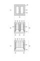
- FIG. 1 is a vertical cross-sectional view showing a schematic structural example of an image plane phase difference pixel according to a first embodiment of the present disclosure
- FIG. FIG. 7 is a vertical cross-sectional view showing a schematic structural example when the image plane phase difference pixel according to the first embodiment of the present disclosure is cut along a plane different from that in FIG. 6
- 1 is a horizontal sectional view showing a schematic structural example of an image plane phase difference pixel according to a first embodiment of the present disclosure
- FIG. FIG. 9 is a horizontal cross-sectional view showing a schematic structural example when the image plane phase difference pixel according to the first embodiment of the present disclosure is cut along a plane different from that in FIG. 8 ;
- FIG. 10 is a process cross-sectional view for explaining the manufacturing method of the solid-state imaging device according to the first embodiment of the present disclosure (part 1);
- FIG. 10 is a process cross-sectional view for explaining the manufacturing method of the solid-state imaging device according to the first embodiment of the present disclosure (part 2);
- FIG. 11 is a process cross-sectional view for explaining the manufacturing method of the solid-state imaging device according to the first embodiment of the present disclosure (No. 3);
- FIG. 12A is a process cross-sectional view for explaining the manufacturing method of the solid-state imaging device according to the first embodiment of the present disclosure (No. 4);
- FIG. 10 is a process cross-sectional view for explaining the manufacturing method of the solid-state imaging device according to the first embodiment of the present disclosure (No. 5);
- FIG. 10A is a process cross-sectional view focusing on the manufacturing process of the pixel separation section in the manufacturing method of the solid-state imaging device according to the first embodiment of the present disclosure (part 1);
- FIG. 11 is a process cross-sectional view focusing on the manufacturing process of the pixel separation section in the manufacturing method of the solid-state imaging device according to the first embodiment of the present disclosure (Part 2);
- FIG. 10 is a process cross-sectional view focusing on the manufacturing process of the pixel separation section in the manufacturing method of the solid-state imaging device according to the first embodiment of the present disclosure (No. 3);
- FIG. 12A is a process cross-sectional view focusing on the manufacturing process of the pixel separation section in the manufacturing method of the solid-state imaging device according to the first embodiment of the present disclosure (No.
- FIG. 10 is a process cross-sectional view focusing on the manufacturing process of the pixel separation section in the manufacturing method of the solid-state imaging device according to the first embodiment of the present disclosure (No. 5);
- FIG. 11 is a process cross-sectional view focusing on the manufacturing process of the pixel separation section in the manufacturing method of the solid-state imaging device according to the first embodiment of the present disclosure (No. 6);
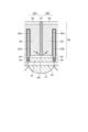
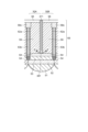
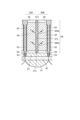
- FIG. 10 is a vertical cross-sectional view showing a schematic structural example of an image plane phase difference pixel during manufacturing according to the first modification of the first embodiment of the present disclosure;
- FIG. 11 is a vertical cross-sectional view showing a schematic structural example of another image plane phase difference pixel in the middle of manufacturing according to the first modification of the first embodiment of the present disclosure;
- FIG. 10 is a vertical cross-sectional view showing a schematic structural example of an image plane phase difference pixel during manufacturing according to the first modification of the first embodiment of the present disclosure
- FIG. 11 is a vertical cross-sectional view showing a schematic structural example
- FIG. 7 is a vertical cross-sectional view showing a schematic structural example of an image plane phase difference pixel according to a second modification of the first embodiment of the present disclosure
- FIG. 11 is a vertical cross-sectional view showing a schematic structural example of an image plane phase difference pixel according to a third modification of the first embodiment of the present disclosure
- FIG. 11 is a vertical cross-sectional view showing a schematic structural example of an image plane phase difference pixel according to a fourth modified example of the first embodiment of the present disclosure
- FIG. 11 is a vertical cross-sectional view showing a schematic structural example of an image plane phase difference pixel according to a fifth modification of the first embodiment of the present disclosure
- 11 is a vertical cross-sectional view showing a schematic structural example of an image plane phase difference pixel according to a sixth modification of the first embodiment of the present disclosure
- 4 is a graph showing the wavelength dependence of refractive index n and bandgap energy k of silicon (Si).
- 7 is a graph showing the wavelength dependence of the refractive index n and bandgap energy k of gallium arsenide (GaAs), which is a candidate material used for the intra-pixel isolation section in the second embodiment of the present disclosure
- 7 is a graph showing the wavelength dependence of the refractive index n and the bandgap energy k of gallium phosphide (GaP), which is a candidate material used for the intra-pixel isolation section in the second embodiment of the present disclosure
- 8 is a graph showing the wavelength dependence of the refractive index n and bandgap energy k of aluminum arsenide (AlAs), which is a candidate material used for the intra-pixel separation section in the second embodiment of the present disclosure
- 7 is a graph showing the wavelength dependence of the refractive index n and bandgap energy k of aluminum antimonide (AlSb), which is a candidate material used for the intra-pixel separation section in the second embodiment of the present disclosure
- 7 is a graph showing the wavelength
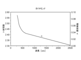
- FIG. 7 is a graph showing the wavelength dependence of the refractive index n of diamond, which is a candidate material used for the intra-pixel separating section in the second embodiment of the present disclosure
- 7 is a graph showing the wavelength dependence of refractive index n and bandgap energy k of DLC, which is a candidate material used for the intra-pixel separation section in the second embodiment of the present disclosure
- 7 is a graph showing the wavelength dependence of refractive index n and bandgap energy k of zinc selenide (ZnSe), which is a candidate material used for the intra-pixel separation section in the second embodiment of the present disclosure
- FIG. 11 is a top view showing a planar structure example of an image plane phase difference pixel according to the third embodiment of the present disclosure
- FIG. 39 is a vertical cross-sectional view showing a structural example of the EE cross section in FIG. 38;
- FIG. 39 is a vertical sectional view showing a structural example of the FF section in FIG. 38;
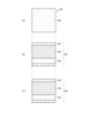
- FIG. 11A is a process cross-sectional view showing a method of manufacturing a solid-state imaging device according to the third embodiment of the present disclosure (Part 1);
- FIG. 11A is a process cross-sectional view showing a method of manufacturing a solid-state imaging device according to the third embodiment of the present disclosure (Part 2);
- FIG. 13A is a process cross-sectional view showing a method of manufacturing a solid-state imaging device according to the third embodiment of the present disclosure (No. 3);
- FIG. 1 is a process cross-sectional view showing a method of manufacturing a solid-state imaging device according to the third embodiment of the present disclosure (Part 1);
- FIG. 11A is a process cross-sectional view showing a method of manufacturing a solid-state imaging device according to the third embodiment of the
- FIG. 14A is a process cross-sectional view showing a method of manufacturing a solid-state imaging device according to the third embodiment of the present disclosure (No. 4);
- FIG. 13A is a process cross-sectional view showing a method for manufacturing a solid-state imaging device according to the third embodiment of the present disclosure (No. 5);
- FIG. 16A is a process cross-sectional view showing a method of manufacturing a solid-state imaging device according to the third embodiment of the present disclosure (No. 6);
- FIG. 16A is a process cross-sectional view showing a method of manufacturing a solid-state imaging device according to the third embodiment of the present disclosure (No. 7);
- FIG. 11 is a vertical cross-sectional view showing a cross-sectional structure example of an image plane phase difference pixel according to the first modified example of the third embodiment of the present disclosure;
- FIG. 11 is a vertical cross-sectional view showing a cross-sectional structure example of an image plane phase difference pixel according to a second modified example of the third embodiment of the present disclosure;
- FIG. 11 is a vertical cross-sectional view showing a cross-sectional structure example of an image plane phase difference pixel according to a third modified example of the third embodiment of the present disclosure;
- FIG. 11 is a vertical cross-sectional view showing a cross-sectional structure example of an image plane phase difference pixel according to a fourth modified example of the third embodiment of the present disclosure;
- FIG. 11 is a vertical cross-sectional view showing a cross-sectional structure example of an image plane phase difference pixel according to the first modified example of the third embodiment of the present disclosure
- FIG. 11 is a vertical cross-sectional view showing a cross-sectional structure example of
- FIG. 11 is a vertical cross-sectional view showing a cross-sectional structure example of an image plane phase difference pixel according to a fifth modified example of the third embodiment of the present disclosure
- FIG. 14 is a vertical cross-sectional view showing a cross-sectional structure example of an image plane phase difference pixel according to a sixth modified example of the third embodiment of the present disclosure
- FIG. 20 is a vertical cross-sectional view showing a cross-sectional structure example of an image plane phase difference pixel according to a seventh modification of the third embodiment of the present disclosure
- FIG. 14 is a vertical cross-sectional view showing a cross-sectional structure example of an image plane phase difference pixel according to a sixth modified example of the third embodiment of the present disclosure
- FIG. 20 is a vertical cross-sectional view showing a cross-sectional structure example of an image plane phase difference pixel according to a seventh modification of the third embodiment of the present disclosure
- FIG. 20 is a vertical cross-sectional view showing a cross-sectional structure example of an image plane phase difference pixel according to an eighth modification of the third embodiment of the present disclosure
- 1 is a block diagram showing an example of a schematic functional configuration of a smart phone
- FIG. 1 is a block diagram showing an example of a schematic configuration of a vehicle control system
- FIG. 4 is an explanatory diagram showing an example of installation positions of an outside information detection unit and an imaging unit
- 1 is a diagram showing an example of a schematic configuration of an endoscopic surgery system
- FIG. 3 is a block diagram showing an example of functional configurations of a camera head and a CCU;
- First Embodiment 1.1 Configuration Example of Electronic Device (Imaging Device) 1.2 Configuration Example of Solid-State Imaging Device 1.3 Configuration Example of Pixel 1.4 Basic Function Example of Pixel 1.5 Layered Structure of Solid-State Imaging Device Example 1.6 Example of basic structure of pixel 1.7 Example of schematic cross-sectional structure of image plane phase difference pixel 1.8 Problems in structure of image plane phase difference pixel 1.9 Example of cross-sectional structure of image plane phase difference pixel 1.10 Manufacturing method 1.11 Summary 1.12 Modifications 1.12.1 First modification 1.12.2 Second modification 1.12.3 Third modification 1.12.4 Fourth modification 1 .12.5 Fifth modification 1.12.6 Sixth modification 2.
- CMOS Complementary Metal-Oxide-Semiconductor
- image sensor Electronic Image Sensor
- the technology according to the present embodiment is applied to various sensors including photoelectric conversion elements, such as CCD (Charge Coupled Device) type solid-state imaging devices, ToF (Time of Flight) sensors, and EVS (Event-based Vision Sensors). It is possible to
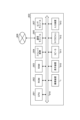
- FIG. 1 is a block diagram showing a schematic configuration example of an electronic device (imaging device) equipped with a solid-state imaging device according to the first embodiment.
- the imaging device 1 includes, for example, an imaging lens 11, a solid-state imaging device 10, a storage unit 14, and a processor 13.
- the imaging lens 11 is an example of an optical system that collects incident light and forms the image on the light receiving surface of the solid-state imaging device 10 .
- the light-receiving surface may be a surface on which the photoelectric conversion elements in the solid-state imaging device 10 are arranged.
- the solid-state imaging device 10 photoelectrically converts incident light to generate image data.
- the solid-state imaging device 10 also performs predetermined signal processing such as noise removal and white balance adjustment on the generated image data.
- the storage unit 14 is composed of, for example, flash memory, DRAM (Dynamic Random Access Memory), SRAM (Static Random Access Memory), etc., and records image data and the like input from the solid-state imaging device 10 .
- the processor 13 is configured using, for example, a CPU (Central Processing Unit), and may include an application processor that executes an operating system and various application software, a GPU (Graphics Processing Unit), a baseband processor, and the like.
- the processor 13 executes various processes as necessary on the image data input from the solid-state imaging device 10 and the image data read from the storage unit 14, executes display for the user, and processes the image data through a predetermined network. or send it to the outside via
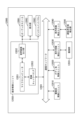
- FIG. 2 is a block diagram showing a schematic configuration example of a CMOS-type solid-state imaging device according to the first embodiment.
- the CMOS-type solid-state imaging device is an image sensor manufactured by applying or partially using a CMOS process.
- the solid-state imaging device 10 according to the present embodiment is configured with a back-illuminated image sensor.
- the solid-state imaging device 10 has, for example, a stack structure in which a light receiving chip 41 (substrate) on which a pixel array section 21 is arranged and a circuit chip 42 (substrate) on which a peripheral circuit is arranged are stacked.
- Peripheral circuits may include, for example, a vertical drive circuit 22 , a column processing circuit 23 , a horizontal drive circuit 24 and a system controller 25 .
- the solid-state imaging device 10 further includes a signal processing section 26 and a data storage section 27 .
- the signal processing unit 26 and the data storage unit 27 may be provided on the same semiconductor chip as the peripheral circuit, or may be provided on a separate semiconductor chip.
- the pixel array section 21 has a configuration in which pixels 30 each having a photoelectric conversion element that generates and accumulates an electric charge according to the amount of received light are arranged in a two-dimensional lattice in rows and columns, that is, in rows and columns.
- the row direction refers to the arrangement direction of pixels in a pixel row (horizontal direction in the drawing)
- the column direction refers to the arrangement direction of pixels in a pixel column (vertical direction in the drawing). Details of the specific circuit configuration and pixel structure of the pixel 30 will be described later.
- pixel drive lines LD are wired along the row direction for each pixel row and vertical signal lines VSL are wired along the column direction for each pixel column with respect to the matrix-like pixel array.
- the pixel drive line LD transmits a drive signal for driving when reading a signal from a pixel.
- the pixel drive lines LD are shown as wirings one by one, but are not limited to one each.
- One end of the pixel drive line LD is connected to an output terminal corresponding to each row of the vertical drive circuit 22 .
- the vertical drive circuit 22 is composed of a shift register, an address decoder, etc., and drives each pixel of the pixel array section 21 simultaneously or in units of rows. That is, the vertical drive circuit 22 constitutes a drive section that controls the operation of each pixel in the pixel array section 21 together with a system control section 25 that controls the vertical drive circuit 22 .
- the vertical drive circuit 22 generally has two scanning systems, a readout scanning system and a discharge scanning system, although the specific configuration thereof is not shown.
- the readout scanning system sequentially selectively scans the pixels 30 of the pixel array section 21 row by row in order to read out signals from the pixels 30 .
- a signal read out from the pixel 30 is an analog signal.
- the sweep-scanning system performs sweep-scanning ahead of the read-out scanning by the exposure time for the read-out rows to be read-scanned by the read-out scanning system.
- a so-called electronic shutter operation is performed by sweeping out (resetting) the unnecessary charges in this sweeping scanning system.
- the electronic shutter operation means an operation of discarding the charge of the photoelectric conversion element and newly starting exposure (starting charge accumulation).
- the signal read out by the readout operation by the readout scanning system corresponds to the amount of light received after the immediately preceding readout operation or the electronic shutter operation.
- the period from the readout timing of the previous readout operation or the sweep timing of the electronic shutter operation to the readout timing of the current readout operation is a charge accumulation period (also referred to as an exposure period) in the pixels 30 .
- a signal output from each pixel 30 in a pixel row selectively scanned by the vertical drive circuit 22 is input to the column processing circuit 23 through each vertical signal line VSL for each pixel column.
- the column processing circuit 23 performs predetermined signal processing on a signal output from each pixel of the selected row through the vertical signal line VSL for each pixel column of the pixel array section 21, and temporarily stores the pixel signal after the signal processing. to be retained.
- the column processing circuit 23 performs at least noise removal processing, such as CDS (Correlated Double Sampling) processing and DDS (Double Data Sampling) processing, as signal processing.
- CDS Correlated Double Sampling
- DDS Double Data Sampling
- the CDS processing removes pixel-specific fixed pattern noise such as reset noise and variations in threshold values of amplification transistors in pixels.
- the column processing circuit 23 also has an AD (analog-digital) conversion function, for example, and converts analog pixel signals read from the photoelectric conversion elements into digital signals and outputs the digital signals.
- AD analog-digital
- the horizontal drive circuit 24 is composed of shift registers, address decoders, etc., and sequentially selects readout circuits (hereinafter also referred to as pixel circuits) corresponding to the pixel columns of the column processing circuit 23 .
- pixel circuits readout circuits
- the system control unit 25 is composed of a timing generator that generates various timing signals. and other drive control.
- the signal processing unit 26 has at least an arithmetic processing function, and performs various signal processing such as arithmetic processing on pixel signals output from the column processing circuit 23 .
- the data storage unit 27 temporarily stores data required for signal processing in the signal processing unit 26 .
- the image data output from the signal processing unit 26 is, for example, subjected to predetermined processing in the processor 13 or the like in the imaging device 1 on which the solid-state imaging device 10 is mounted, or is transmitted to the outside via a predetermined network. You may
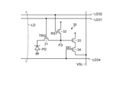
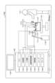
- FIG. 3 is a circuit diagram showing a schematic configuration example of a pixel according to this embodiment.
- the pixel 30 includes a photoelectric conversion unit PD, a transfer transistor 31, a reset transistor 32, an amplification transistor 33, a selection transistor 34, and a floating diffusion region FD.
- a select transistor drive line LD34 included in the pixel drive line LD is connected to the gate of the select transistor 34, a reset transistor drive line LD32 included in the pixel drive line LD is connected to the gate of the reset transistor 32, and a transfer transistor is connected. 31 is connected to a transfer transistor drive line LD31 included in the pixel drive line LD.
- a vertical signal line VSL one end of which is connected to the column processing circuit 23 , is connected to the source of the amplification transistor 33 via the selection transistor 34 .
- the reset transistor 32, amplification transistor 33, and selection transistor 34 are also collectively referred to as a pixel circuit.
- This pixel circuit may include a floating diffusion region FD and/or a transfer transistor 31 .
- the photoelectric conversion unit PD photoelectrically converts incident light.
- the transfer transistor 31 transfers charges generated in the photoelectric conversion unit PD.
- the floating diffusion region FD functions as a charge accumulation portion that accumulates charges transferred by the transfer transistor 31 .
- the amplification transistor 33 causes a pixel signal having a voltage value corresponding to the charge accumulated in the floating diffusion region FD to appear on the vertical signal line VSL.
- the reset transistor 32 releases charges accumulated in the floating diffusion region FD.
- the selection transistor 34 selects the pixel 30 to be read.
- the photoelectric conversion unit PD has an anode grounded and a cathode connected to the source of the transfer transistor 31 .
- the drain of the transfer transistor 31 is connected to the source of the reset transistor 32 and the gate of the amplification transistor 33, and the node that is the connection point of these constitutes the floating diffusion region FD.
- a drain of the reset transistor 32 is connected to a vertical reset input line (not shown).
- the drain of the amplification transistor 33 is connected to a vertical voltage supply line (not shown).
- the source of the amplification transistor 33 is connected to the drain of the selection transistor 34, and the source of the selection transistor 34 is connected to the vertical signal line VSL.
- the potential of the floating diffusion region FD is determined by the charge accumulated there and the capacitance of the floating diffusion region FD.
- the capacitance of the floating diffusion region FD is determined by the drain diffusion layer capacitance of the transfer transistor 31, the source diffusion layer capacitance of the reset transistor 32, the gate capacitance of the amplification transistor 33, and the like, in addition to the capacitance to ground.
- the reset transistor 32 controls discharge (reset) of charges accumulated in the floating diffusion region FD according to a reset signal RST supplied from the vertical drive circuit 22 via a reset transistor drive line LD32.
- a reset signal RST supplied from the vertical drive circuit 22 via a reset transistor drive line LD32.
- the photoelectric conversion unit PD photoelectrically converts incident light and generates charges according to the amount of light. The generated charge is accumulated on the cathode side of the photoelectric conversion unit PD.
- the transfer transistor 31 controls charge transfer from the photoelectric conversion unit PD to the floating diffusion region FD according to a transfer control signal TRG supplied from the vertical drive circuit 22 via the transfer transistor drive line LD31.
- the potential of the floating diffusion region FD when the reset transistor 32 is off is determined by the amount of charge transferred from the photoelectric conversion unit PD via the transfer transistor 31 and the capacitance of the floating diffusion region FD, as described above.
- the amplification transistor 33 functions as an amplifier whose input signal is the potential fluctuation of the floating diffusion region FD connected to its gate, and its output voltage signal appears as a pixel signal on the vertical signal line VSL via the selection transistor 34 .
- the selection transistor 34 controls the appearance of the pixel signal by the amplification transistor 33 on the vertical signal line VSL according to the selection control signal SEL supplied from the vertical drive circuit 22 via the selection transistor drive line LD34. For example, when a High-level selection control signal SEL is input to the gate of the selection transistor 34, a pixel signal from the amplification transistor 33 appears on the vertical signal line VSL. On the other hand, when the Low level selection control signal SEL is input to the gate of the selection transistor 34, the appearance of the pixel signal to the vertical signal line VSL is stopped. This makes it possible to take out only the output of the selected pixel 30 on the vertical signal line VSL to which the plurality of pixels 30 are connected.
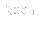
- FIG. 4 is a diagram showing a layered structure example of the image sensor according to the present embodiment.
- the solid-state imaging device 10 has a structure in which a light receiving chip 41 and a circuit chip 42 are vertically stacked.
- the light receiving chip 41 has a structure in which the light receiving chip 41 and the circuit chip 42 are laminated.
- the light-receiving chip 41 is, for example, a semiconductor chip including the pixel array section 21 in which the photoelectric conversion sections PD are arranged
- the circuit chip 42 is, for example, a semiconductor chip in which pixel circuits are arranged.
- so-called direct bonding can be used in which the respective bonding surfaces are flattened and the two are bonded together by inter-electron force.
- so-called Cu—Cu bonding in which electrode pads made of copper (Cu) formed on the mutual bonding surfaces are bonded together, or bump bonding.
- the light receiving chip 41 and the circuit chip 42 are electrically connected via a connecting portion such as a TSV (Through-Silicon Via), which is a through contact penetrating the semiconductor substrate.
- Connection using TSVs includes, for example, a so-called twin TSV method in which two TSVs, a TSV provided on the light receiving chip 41 and a TSV provided from the light receiving chip 41 to the circuit chip 42, are connected on the outside of the chip.
- a so-called shared TSV system or the like can be adopted in which the chip 41 and the circuit chip 42 are connected by a TSV penetrating therethrough.
- FIG. 5 is a cross-sectional view showing a basic cross-sectional structure example of a pixel according to the first embodiment. Note that FIG. 5 shows a cross-sectional structure example of the light receiving chip 41 in which the photoelectric conversion unit PD in the pixel 30 is arranged.
- the photoelectric conversion unit PD receives incident light L1 incident from the back surface (upper surface in the figure) side of the semiconductor substrate 58. As shown in FIG. A planarizing film 53, a color filter 52, and an on-chip lens 51 are provided above the photoelectric conversion unit PD. photoelectric conversion is performed.
- the semiconductor substrate 58 includes, for example, a semiconductor substrate made of a group IV semiconductor made of at least one of carbon (C), silicon (Si), germanium (Ge) and tin (Sn), or a semiconductor substrate made of boron (B). ), aluminum (Al), gallium (Ga), indium (In), nitrogen (N), phosphorus (P), arsenic (As), and antimony (Sb).
- a semiconductor substrate made of a semiconductor may be used. However, it is not limited to these, and various semiconductor substrates may be used.
- the photoelectric conversion part PD may have, for example, a structure in which the N-type semiconductor region 59 is formed as a charge accumulation region that accumulates charges (electrons).
- the N-type semiconductor region 59 is provided within a region surrounded by the P-type semiconductor regions 56 and 64 of the semiconductor substrate 58 .
- a P-type semiconductor region 64 having an impurity concentration higher than that on the back surface (upper surface) side of the semiconductor substrate 58 is provided on the N-type semiconductor region 59 on the front surface (lower surface) side of the semiconductor substrate 58 .
- the photoelectric conversion unit PD has a HAD (Hole-Accumulation Diode) structure, and in order to suppress the generation of dark current at each interface between the upper surface side and the lower surface side of the N-type semiconductor region 59, P-type semiconductor regions 56 and 64 are provided.
- HAD Hole-Accumulation Diode
- a pixel separation section 60 for electrically separating the plurality of pixels 30 is provided inside the semiconductor substrate 58.
- the pixel separation section 60 is provided in a lattice shape so as to be interposed between the plurality of pixels 30, for example, and the photoelectric conversion section PD It is arranged in a region partitioned by the pixel separation section 60 .
- each photoelectric conversion unit PD the anode is grounded, and in the solid-state imaging device 10, signal charges (for example, electrons) accumulated in the photoelectric conversion unit PD are transferred through a transfer transistor 31 (see FIG. 3) (not shown) or the like. and output as an electrical signal to a vertical signal line VSL (see FIG. 3), not shown.
- a transfer transistor 31 see FIG. 3 (not shown) or the like.
- the wiring layer 65 is provided on the surface (lower surface) of the semiconductor substrate 58 opposite to the back surface (upper surface) on which the light shielding film 54, the planarizing film 53, the color filter 52, the on-chip lens 51, and the like are provided. be done.
- the wiring layer 65 is composed of a wiring 66, an insulating layer 67, and a through electrode (not shown). An electric signal from the light receiving chip 41 is transmitted to the circuit chip 42 via the wiring 66 and through electrodes (not shown). Similarly, the substrate potential of the light receiving chip 41 is also applied from the circuit chip 42 via the wiring 66 and through electrodes (not shown).
- the circuit chip 42 illustrated in FIG. 4 is bonded to the surface of the wiring layer 65 opposite to the side on which the photoelectric conversion part PD is provided.
- the light shielding film 54 is provided on the back surface (upper surface in the drawing) of the semiconductor substrate 58 and blocks part of the incident light L1 directed from above the semiconductor substrate 58 toward the back surface of the semiconductor substrate 58 .
- the light shielding film 54 is provided above the pixel separation section 60 provided inside the semiconductor substrate 58 .
- the light shielding film 54 is provided on the rear surface (upper surface) of the semiconductor substrate 58 so as to protrude in a convex shape through an insulating film 55 such as a silicon oxide film.
- the photoelectric conversion unit PD provided inside the semiconductor substrate 58, the light shielding film 54 is not provided and is open so that the incident light L1 is incident on the photoelectric conversion unit PD. ing.
- the planar shape of the light shielding film 54 is a lattice shape, and openings are formed through which the incident light L1 passes to the light receiving surface 57 .
- the light shielding film 54 is made of a light shielding material that shields light.
- the light shielding film 54 is formed by sequentially laminating a titanium (Ti) film and a tungsten (W) film.
- the light-shielding film 54 can be formed by sequentially laminating a titanium nitride (TiN) film and a tungsten (W) film, for example.
- the light shielding film 54 is covered with the planarizing film 53 .
- the planarizing film 53 is formed using an insulating material that transmits light. Silicon oxide (SiO 2 ), for example, can be used for this insulating material.
- the pixel separation section 60 has, for example, a groove 61 , a fixed charge film 62 , and an insulating film 63 . is provided to cover the
- the fixed charge film 62 is provided so as to cover the inner surface of the groove 61 formed on the back surface (upper surface) side of the semiconductor substrate 58 with a constant thickness.
- An insulating film 63 is provided (filled) so as to bury the inside of the trench 61 covered with the fixed charge film 62 .
- the fixed charge film 62 a high dielectric material having negative fixed charges is used so that a positive charge (hole) accumulation region is formed at the interface with the semiconductor substrate 58 and generation of dark current is suppressed. formed by Since the fixed charge film 62 has negative fixed charges, the negative fixed charges apply an electric field to the interface with the semiconductor substrate 58 to form a positive charge (hole) accumulation region.
- the fixed charge film 62 can be formed of, for example, a hafnium oxide film (HfO 2 film).
- the fixed charge film 62 can also be formed to contain at least one of oxides of hafnium, zirconium, aluminum, tantalum, titanium, magnesium, yttrium, lanthanide elements, and the like.
- the pixel separating section 60 is not limited to the configuration described above, and can be variously modified.
- a reflective film that reflects light such as a tungsten (W) film
- the pixel separation section 60 can have a light reflective structure.
- the incident light L1 entering the photoelectric conversion unit PD can be reflected by the pixel separation unit 60, so that the optical path length of the incident light L1 within the photoelectric conversion unit PD can be increased.
- the pixel separating section 60 have a light reflecting structure, it is possible to reduce the leakage of light into adjacent pixels, so that it is possible to further improve the image quality, distance measurement accuracy, and the like.
- a metal material such as tungsten (W)
- the configuration in which the pixel separating section 60 has a light reflecting structure is not limited to the configuration using a reflective film. can do.
- FIG. 5 illustrates a pixel isolation portion 60 having a so-called RDTI (Reverse Deep Trench Isolation) structure in which the pixel isolation portion 60 is provided in a groove portion 61 formed from the back surface (upper surface) side of the semiconductor substrate 58.
- RDTI Reverse Deep Trench Isolation
- FTI Frull Trench Isolation
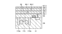
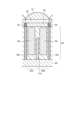
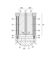
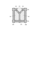
- FIG. 6 is a vertical sectional view showing a schematic structural example of an image plane phase difference pixel according to this embodiment.
- the same components as those in FIG. 5 are denoted by the same reference numerals, and overlapping descriptions are omitted.
- the configuration shown in FIG. 5 and the configuration shown in FIG. 6 are slightly changed in the portions other than the characteristic configuration of the present embodiment within the scope of the technical matters related to the present disclosure.
- the pixel structure is omitted or simplified as necessary in FIG. 6 and the following explanation.
- the image plane phase difference pixel has a structure in which two pixels 30A and 30B share one on-chip lens 51 and one color filter 52.
- the two pixels 30A and 30B adjacent in the row direction or the column direction constitute one image plane phase difference pixel, that is, the two pixels 30A and 30B form one on-chip lens 51 and 1
- a case where two color filters 52 are shared is exemplified, but is not limited to this.
- a pair of pixels 30A and 30B forming one image plane phase difference pixel and other pixels 30 arranged to surround them are optically and electrically separated by a pixel separating section 60.
- FIG. 6 illustrates a case where the pixel separation section 60 has a so-called FTI structure (penetration structure) that penetrates the semiconductor substrate 58 .
- FTI structure penetration structure
- FIGS. 7 to 9, 11 to 22, and 27 which will be described later, the structure of the pixel separation section 60 is illustrated in a simplified manner.
- a pixel separation unit for example, a rectangular region
- an intra-pixel isolation section 170 for electrical isolation.
- the in-pixel isolation part 170 arranged between the pixels 30A and 30B penetrates the semiconductor substrate 58 from the back surface (corresponding to the light incident surface) side of the semiconductor substrate 58 toward the front surface (corresponding to the element forming surface) side, for example. It has a so-called DTI structure (non-penetrating structure) that extends to the extent that it does not.
- the separating portion (intra-pixel separating portion 170) between the pixels 30A and 30B that constitute one image plane phase difference pixel non-penetrating structure
- a part of the semiconductor substrate 58 is used to separate the pixels 30A and 30B. It becomes a continuous structure straddling.
- a continuous portion of the semiconductor substrate 58 functions as an inter-color path (hereinafter also referred to as an overflow path) for releasing carriers to the other pixel when one of the pixels 30A and 30B is saturated.
- the pixels 30A and 30B forming one image plane phase difference pixel are so-called same-color pixels that share the same color filter 52. Therefore, by electrically connecting the pixels 30A and 30B with an overflow path, It is possible to reduce the difference in photosensitivity between the pixels 30A and 30B due to process errors and the like.
- the photoelectric conversion portion PD the N-type semiconductor region 59 and the P-type semiconductor regions 56 and 64 (see FIG. 5) surrounding it) in one of the right pixels
- the generated electrons are sequentially transferred to the floating diffusion region FD of the pixel circuit via the transfer transistor 31 and read out as pixel signals of the pixels 30A and 30B.
- the signal processing unit 26 to which the read pixel signals are input detects the phase difference by comparing the signal amounts of the left pixel 30A and the right pixel 30B, and determines an appropriate focal length based on the detected phase difference.
- the separation material between different color pixels i.e., the material of the pixel separation portion 60
- the material for separating pixels of the same color that is, the material of the intra-pixel isolation part 170
- the pixel separation section 60 and the intra-pixel separation section 170 are required to have different characteristics. In this way, when the required properties are different, there is a problem that it is not possible to easily produce different internal materials.
- the in-pixel separation section 170 which has a non-penetration structure
- the in-pixel isolation section 170 is provided between the pixel isolation section 60 (or through hole or trench in which it is formed) and the in-pixel isolation section 170 (or trench in which it is formed).
- the structure is such that a layer or region that functions as an etching stopper during processing (that is, when removing the film formed around the image plane phase difference pixel) is arranged.
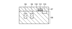
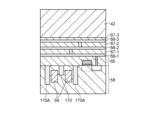
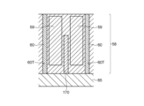
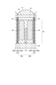
- FIG. 7 is a vertical cross-sectional view showing an example of the schematic structure of the image plane phase difference pixel according to the present embodiment, cut along a plane different from that in FIG. 6 is a cross-sectional view of the light-receiving chip 41 cut along a plane (DD plane) that is perpendicular to the element formation surface of the semiconductor substrate 58 and parallel to the arrangement direction of the pixels 30A and 30B.
- DD plane plane
- AA plane that is perpendicular to the device formation surface of the semiconductor substrate 58 and parallel to the arrangement direction of the pixels 30A and 30B. showing.
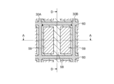
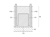
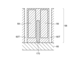
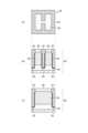
- FIG. 8 is a horizontal cross-sectional view showing a schematic structural example of the image plane phase difference pixel according to the present embodiment, and FIG. It is a horizontal sectional view showing an example of a schematic structure when cut. 8 shows an example of the cross-sectional structure along the CC plane in FIGS. 6 and 7, and FIG. 9 shows an example of the cross-sectional structure along the DD plane in FIGS.
- the image plane phase difference pixel has, for example, a rectangular image plane phase difference pixel region partitioned by a pixel separating unit 60 provided between the image plane phase difference pixels. , divided into two, for example, rectangular pixel regions by an intra-pixel separating portion 170 arranged so as to pass through the center of the pixel region.
- the material of the pixel separation section 60 is, for example, silicon oxide (SiO 2 ), tungsten (W), aluminum (Al), or any other material having high reflectance and high insulation properties. may be used.
- materials for the in-pixel isolation portion 170 include diamond, DLC (Diamond-like Carbon), titanium oxide (TiO 2 ), cerium oxide (CeO 2 ), iron oxide (Fe 2 O 3 ), and silicon nitride (SiN).
- DLC Diamond-like Carbon
- TiO 2 titanium oxide
- CeO 2 cerium oxide
- Fe 2 O 3 iron oxide
- SiN silicon nitride
- One or more materials with properties of low reflectivity, low insulating properties, and non-photovoltaic properties, such as, may be used.
- At least a partial region between the pixel isolation portion 60 and the in-pixel isolation portion 170 can have a sufficient etching selectivity with respect to the material used for the in-pixel isolation portion 170.
- a layer or region (hereinafter also referred to as an etching stopper region 101) is arranged.
- a partial region of the semiconductor substrate 58 can be used as the etching stopper region 101 .
- the in-pixel isolation portion 170 is made of a material that can have a sufficient etching selectivity with respect to the material (for example, silicon (Si)) forming the semiconductor substrate 58 .
- the pixel Since it is possible to greatly reduce the area removed from the inner isolation section 170, it is possible to easily separately produce the pixel isolation section 60 and the intra-pixel isolation section 170 having different required characteristics.
- the transfer transistor 31 is the photoelectric conversion unit.
- the PD is arranged on the same light receiving chip 41
- at least one transistor other than the transfer transistor 31 may also be arranged on the light receiving chip 41 .
- 10 to 14 are process cross-sectional views for explaining the manufacturing method of the solid-state imaging device according to this embodiment.
- 15 to 20 are process cross-sectional views focusing on the manufacturing process of the pixel separation section in the manufacturing method of the solid-state imaging device according to this embodiment.
- a semiconductor substrate (for example, a silicon wafer) 58 having P-type conductivity is prepared. form 59.
- the N-type semiconductor region 59 in the semiconductor substrate 58 is formed in a predetermined region from the surface side of the semiconductor substrate 58 with predetermined implantation energy and dose using, for example, a photoresist or a hard mask formed using a lithographic technique.
- predetermined implantation energy and dose using, for example, a photoresist or a hard mask formed using a lithographic technique.
- the transfer transistor 31 is formed on the element formation surface of the semiconductor substrate 58 , and the element formation surface of the semiconductor substrate 58 on which the transfer transistor 31 is formed is covered with an insulating layer 67 .
- a gate insulating film 132 and a gate electrode 131 are formed in a predetermined region on the semiconductor substrate 58, and then a predetermined dopant is ion-implanted in a predetermined region on the element formation surface to form a diffusion region 133. is formed.
- the diffusion region 133 thus formed and the diffusion region forming the cathode of the photoelectric conversion unit PD function as the source/drain of the transfer transistor 31 .
- the insulating layer 67 can be formed by, for example, a CVD (Chemical Vapor Deposition) method, sputtering, or the like.
- the upper surface of the insulating layer 67 may be planarized by, for example, CMP (Chemical Mechanical Polishing).
- a first trench also referred to as a through trench
- a second trench also referred to as a non-penetrating trench
- a lithography technique for example, can be used to form the first and second trenches. That is, a resist film or a hard mask is formed on the element formation surface of the semiconductor substrate 58 by photolithography, and the semiconductor substrate 58 is etched through the mask by dry etching such as RIE (Reactive Ion Etching), First and second trenches may be formed.
- RIE Reactive Ion Etching
- the RIE etching conditions for digging the first trench and the second trench may be set as follows, for example. Chamber pressure: 5 to 100 (mTorr (millitorr) Source power: 500-2000 (W (Watt)) Bias power: 100-1000 (W) Chlorine gas flow: 10 to 300 sccm (Cubic Centimeter per Minute) Oxygen gas flow: 1-50sccm
- the opening width (also called line width) of the mask when forming the first and second trenches may be, for example, about 0.01 ⁇ m (micrometers) to 0.5 ⁇ m.
- the depth of the first trench after processing may be, for example, 0.1 ⁇ m or more.
- the first trench and the second trench can be made in the same step by adjusting the line width of the mask, but they may be made in separate steps. That is, by adjusting the line width of the mask to control the etching rate in the depth direction, it is possible to form the first trench and the second trench having different depths in the same process.
- the contact holes for forming the wirings 66 in contact with the gate electrode 131 and the diffusion regions, respectively may be formed in the same process as the formation of the first and/or second trenches, or may be formed in a separate process. good too.
- the intra-pixel isolation section 170 is formed in the second trench by embedding a predetermined material in the second trench using, for example, a CVD (Chemical Vapor Deposition) method, sputtering, or the like.
- the predetermined material may be a material with low reflectivity, low insulating properties, and non-photoelectric conversion properties, as described above.
- a film 170A made of the same material as the in-pixel isolation section 170 may be formed in the first trench.
- the material deposited on the device forming surface of the semiconductor substrate 58 may be removed by a method such as CMP (Chemical Mechanical Polishing) or lift-off.
- the openings formed in the insulating layer 67 for forming the in-pixel isolation section 170 and the film 170A may be filled with the same material as the insulating layer 67 .
- wiring layers 68-1, 68-2 and 68-3 electrically connected to circuit elements such as the transfer transistor 31 and interlayer wiring layers 68-1, 68-2 and 68-3 are formed on the element forming surface of the semiconductor substrate 58. and via wirings 66-1 and 66-2 electrically connecting wiring layers 68-1, 68-2 and 68-3 of each layer. forming a multilayer wiring layer including
- a circuit chip 42 made of, for example, a silicon substrate is pasted on the multilayer wiring layer.
- Bonding between the chips can be performed by, for example, direct bonding in which the top surface of the multilayer wiring layer and the bonding surface of the circuit chip 42 are each flattened and bonded together by electron-electron force, or copper (copper) formed on the top surface of the multilayer wiring layer.
- Various bonding methods are used, such as a bonding form (Cu—Cu bonding) in which a metal pad made of Cu) and a metal pad made of copper (Cu) formed on the bonding surface of the circuit chip 42 are bonded together. good.
- the semiconductor substrate 58 on which the circuit chip 42 is bonded is turned over on the element forming surface side, and the thickness of the semiconductor substrate 58 is thinned with high precision from the back surface (light incident surface) side. , exposes the bottom of the film 170A embedded in the first trench where the pixel isolation part 60 is formed.
- One or a combination of two or more of CMP, dry etching, wet etching, and the like may be used to thin the semiconductor substrate 58 . It should be noted that this thinning step does not exclude that at least a portion of the bottom of membrane 170A is removed.
- FIGS. 16, 18 and 20 are process cross-sectional views corresponding to FIG. 7 described above.
- the first trench in which the pixel isolation section 60 is formed is made of the same material as the in-pixel isolation section 170.
- a membrane 170A is formed. Therefore, for example, if an attempt is made to remove the film 170A by an isotropic etching method such as wet etching, there is a possibility that the intra-pixel isolation portion 170 made of the same material will be removed over a wide area.
- the in-pixel isolation portion is formed at least partially between the film 170A formed in the first trench and the in-pixel isolation portion 170 formed in the second trench.
- An etching stopper region 101 made of a material capable of ensuring an etching selectivity with respect to the constituent material of 170 is arranged. As a result, it is possible to prevent or suppress removal of a part of the in-pixel separation section 170 when removing the film 170A. It becomes possible to separate them.
- the constituent material of the etching stopper region 101 can be, for example, the constituent material of the semiconductor substrate 58 (that is, part of the semiconductor substrate 58). As a result, it is possible to avoid complication of the manufacturing process, so that it is possible to suppress a decrease in yield.
- the film 170A is removed from the back surface (the top surface in FIGS. 17 and 18) of the semiconductor substrate 58 by wet etching, for example.
- an etchant that can ensure an etching selectivity with respect to the material forming the etching stopper region 101 (the material of the semiconductor substrate 58 in this example) may be used.
- the etching stopper region 101 prevents or restricts the contact of the etchant with the in-pixel isolation section 170, thereby preventing or suppressing the removal of part of the in-pixel isolation section 170 when removing the film 170A. becomes possible.
- the trenches 60T formed by removing the film 170A are filled with a material having high reflectivity and high insulating properties to form the pixel separation section 60.
- a film forming technique such as CVD or sputtering may be appropriately used for forming the pixel separation section 60 .
- the pixel separation section 60 may have a laminated structure of a fixed charge film 62 made of a high dielectric constant material and an insulating film 63 or a metal film. Materials deposited on the back surface of the semiconductor substrate 58 may also be removed by CMP, wet etching, or the like.
- a solid-state imaging device 10 having an image plane phase difference pixel having a cross-sectional structure illustrated in 9 is manufactured.
- At least a portion between the pixel isolation portion 60 and the in-pixel isolation portion 170 has an etching selectivity with respect to the constituent material of the in-pixel isolation portion 170 .
- An etching stopper region 101 made of a material that can be etched is arranged. Accordingly, in the manufacturing process, when removing the film 170A made of the same material as the in-pixel isolation part 170 formed in the trench (first trench) in which the pixel isolation part 60 is formed, one part of the in-pixel isolation part 170 is removed.
- the part 60 and the intra-pixel separation part 170 can be easily separately produced.
- high refractive index that is, low reflectance
- high insulation that is, high insulation
- non-photoelectric conversion characteristics are achieved between pixels of the same color.
- the separation structure between pixels of the same color a physical structure rather than a separation structure by an ion diffusion region, it is possible to relax the electric field to the floating diffusion region FD on the side of the separation.
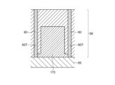
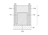
- FIG. 21 is an example of a cross-sectional structure of an image-plane phase difference pixel in the middle of manufacturing according to a first modification, and is a vertical cross-sectional structure example in a step corresponding to FIG. It is a sectional view.
- the etching stopper region 101 is arranged at least partly between the pixel isolation portion 60 (or the film 170A) and the in-pixel isolation portion 170 .
- the pixel separation section 60 (or the film 170A) and the in-pixel separation section 170 are connected on the back side of the semiconductor substrate 58, as illustrated in FIGS.
- the pixel separation section 60 (or film 170A) and the intra-pixel separation section 170 may be completely separated by the etching stopper region 102 .
- the etching stopper region 102 may be arranged in the entire range between the pixel isolation portion 60 (or the film 170A) and the in-pixel isolation portion 170 .
- the pixel isolation portion 60 (or the film 170A) and the intra-pixel isolation portion 170 are completely separated by the etching stopper region 102, so that the intra-pixel isolation portion 170 is removed when the film 170A is removed. can be prevented or strongly suppressed, the pixel separation section 60 and the in-pixel separation section 170 having different required characteristics can be produced more easily. As a result, it is possible to easily realize a configuration capable of suppressing a decrease in photosensitivity.
- FIG. 22 is another cross-sectional structure example of the image plane phase difference pixel in the middle of manufacturing according to the first modified example, and is a cross-sectional view showing a cross-sectional structure example in the process corresponding to FIG.
- only one side of the intra-pixel isolation portion 170 may be completely isolated from the pixel isolation portion 60 (or film 170A). With this configuration as well, it is possible to prevent or strongly suppress the removal of the in-pixel separation section 170 when removing the film 170A. It is possible to separate them into
- FIG. 23 is a vertical cross-sectional view showing a schematic structural example of an image plane phase difference pixel according to a second modification, which corresponds to the cross-sectional structure illustrated in FIG.
- FIG. 4 is a vertical sectional view showing an example
- the pixel separating section 60 is replaced with a pixel separating section 161 made of an insulating film. That is, in the second modification, the fixed charge film 62 is omitted, and the inside of the first trench (corresponding to the groove portion 61) is filled with the insulating film 63.
- FIG. 23 in the second modified example, the pixel separating section 60 is replaced with a pixel separating section 161 made of an insulating film. That is, in the second modification, the fixed charge film 62 is omitted, and the inside of the first trench (corresponding to the groove portion 61) is filled with the insulating film 63.
- FIG. 24 is a vertical cross-sectional view showing a schematic structural example of an image plane phase difference pixel according to a third modification, the cross-sectional structure corresponding to the cross section illustrated in FIG. FIG. 4 is a vertical sectional view showing an example;
- the pixel separating section 60 is replaced with a pixel separating section 162 made of a light shielding film.
- a light shielding material such as tungsten (W) or aluminum (Al) can be used as the material.
- a conductive material is used for the pixel separating portion 162
- the inner surface of the first trench (groove portion 61) is made of an insulating film such as a silicon oxide film (SiO 2 ) or a silicon nitride film (SiN), a fixed charge film, or the like. may be covered with
- the laminated structure may be a laminated structure of aluminum (Al)/titanium (Ti)-based barrier metal, a laminated structure of aluminum (Al)/cobalt (Co), or the like.
- the inner surface of the first trench (trench portion 61) is an insulating film such as a silicon oxide film (SiO 2 ) or a silicon nitride film (SiN). or a fixed charge film or the like.
- the pixel separation section 162 is made of the same material as the light shielding film 54 thereon, the pixel separation section 162 and the light shielding film 54 may be made of an integrated film.
- FIG. 25 is a vertical cross-sectional view showing a schematic structural example of an image plane phase difference pixel according to a fourth modification, the cross-sectional structure corresponding to the cross-section illustrated in FIG. FIG. 4 is a vertical sectional view showing an example;
- the pixel separation section 60 includes an insulating film (SCF: Silicon Cover Film) 163b having fixed charges that covers the inner surface of the first trench (groove section 61) and the first trench It is replaced with a pixel separating portion 163 composed of an insulating film 163a filling the inside.
- SCF Silicon Cover Film
- the insulating film 163a may be the same as the insulating film 63 described above, for example.
- the insulating film (SCF) 163b has, for example, a negative fixed charge due to a dipole of oxygen, and by being in contact with the surface of the semiconductor substrate 58, can serve to strengthen the pinning of the photoelectric conversion unit PD.
- the material of the insulating film 163b is, for example, oxide or nitride containing at least one of hafnium (Hf), aluminum (Al), zirconium (Zr), tantalum (Ta), titanium (Ti), and the like. can be used. Also, lanthanum (La), cerium (Ce), neodymium, promethium (Pm), samarium (Sm), europium (Eu), gadolinium (Gd), terbium (Tb), dysprosium (Dy), holmium (Ho), thulium (Tm), ytterbium (Yb), lutetium (Lu), yttrium (Y), etc., may also be used.
- oxide or nitride containing at least one of hafnium (Hf), aluminum (Al), zirconium (Zr), tantalum (Ta), titanium (Ti), and the like.
- La lanthanum
- Ce cerium
- the insulating film 163b may be made of hafnium oxynitride or aluminum oxynitride. Further, the insulating film 163b may be doped with silicon or nitrogen in an amount that does not impair the insulating properties. Thereby, heat resistance etc. can be improved.
- FIG. 26 is a vertical cross-sectional view showing a schematic structural example of an image plane phase difference pixel according to a fifth modification, the cross-sectional structure corresponding to the cross section illustrated in FIG. FIG. 4 is a vertical sectional view showing an example;
- the pixel isolation portion 60 includes an insulating film (SCF) 164b having fixed charges covering the inner surface of the first trench (trench portion 61) and a light shielding film filling the inside of the first trench. It is replaced with a pixel separation section 164 composed of a film 164a.
- SCF insulating film
- the insulating film 164b may be the same as the insulating film 163b according to the fourth embodiment, for example.
- the light shielding film 164a is, for example, a single layer film of tungsten (W) or aluminum (Al), a laminated structure of aluminum (Al)/titanium (Ti) based barrier metal, or an aluminum (Al)/cobalt (Co) film. may be a multilayer film of
- FIG. 27 is a vertical cross-sectional view showing a schematic structural example of an image-plane phase difference pixel according to a sixth modification, the cross-sectional structure corresponding to the cross-section illustrated in FIG. FIG. 4 is a vertical sectional view showing an example;
- the intra-pixel separation section 170 has a shape in which the width of the upper end and the width of the lower end are substantially equal. That is, the case where the cross-sectional shape of the intra-pixel separating portion 170 in the vertical plane (corresponding to the DD plane) parallel to the arrangement direction of the pixels 30A and 30B is rectangular is exemplified.
- the intra-pixel separating portion 171 has a shape in which the width of the upper end is narrower than the width of the lower end, that is, the arrangement direction of the pixels 30A and 30B
- the cross-section of the intra-pixel separating portion 170 on a vertical plane (corresponding to the DD plane) parallel to 1 may have a vertically elongated trapezoidal or triangular shape.
- the isolation material between pixels of different colors (that is, the material of the pixel isolation section 60) is required to have characteristics of high reflectance and high insulation.
- a material for separating pixels of the same color (that is, a material for the intra-pixel separating portion 170) is required to have properties such as low reflectance, low insulation, and non-photoelectric conversion properties.
- FIG. 28 is a graph showing the wavelength dependence of the refractive index n and bandgap energy k of silicon (Si).
- FIG. 29 is a graph showing the wavelength dependence of the refractive index n and bandgap energy k of gallium arsenide (GaAs).
- the intra-pixel separating section 170 In order for the intra-pixel separating section 170 that separates the two pixels 30A and 30B constituting one image plane phase difference pixel to have low reflectance, low insulation, and non-photoelectric conversion characteristics, the intra-pixel separating section 170 is It is desirable to use a material having a refractive index n close to that of the semiconductor substrate 58 and a wide bandgap energy.
- the semiconductor substrate 58 is a silicon substrate, as shown in FIG. 28, the refractive index n of Si for light with a wavelength of 500 nm is 4 or more, and the bandgap energy k for light with a wavelength of 500 nm is approximately 1.12 eV (electron volt).
- GaAs is presented as a constituent material of the intra-pixel isolation section 170 .
- the refractive index n of GaAs for light with a wavelength of 500 nm is 4 or more, which is equivalent to that of Si (4 or more)
- the bandgap energy k for light with a wavelength of 500 nm is that of Si (about 1 .12 eV), which is about 1.43 eV.
- GaAs As a constituent material of the in-pixel isolation portion 170, photoelectric conversion in the in-pixel isolation portion 170 can be suppressed while suppressing reflection at the interface between the semiconductor substrate 50 and the in-pixel isolation portion 170. becomes possible. Since GaAs is a compound semiconductor, it is possible to achieve low insulation.
- FIG. 30 is a graph showing the wavelength dependence of the refractive index n and bandgap energy k of gallium phosphide (GaP).
- the refractive index n of GaP for light with a wavelength of 500 nm is about 3.5, which is slightly lower than that of Si (4 or more), and the bandgap energy k for light with a wavelength of 500 nm is Si is about 2.3 eV, which is larger than that of (about 1.12 eV).
- GaP is a constituent material of the in-pixel isolation section 170, the reflection at the interface between the semiconductor substrate 50 and the in-pixel isolation section 170 is suppressed, as in the above-described example. photoelectric conversion can be suppressed. Since GaP is a compound semiconductor, it is possible to achieve low insulation.
- FIG. 31 is a graph showing the wavelength dependence of the refractive index n and bandgap energy k of aluminum arsenide (AlAs).
- the refractive index n of AlAs for light with a wavelength of 500 nm is about 3.25, which is slightly lower than that of Si (4 or more), and the bandgap energy k for light with a wavelength of 500 nm is Si is about 2.12 eV, which is larger than that of (about 1.12 eV).
- GaP As a constituent material of the in-pixel isolation section 170, the reflection at the interface between the semiconductor substrate 50 and the in-pixel isolation section 170 is suppressed, as in the above-described example. photoelectric conversion can be suppressed. Since AlAs is a semiconductor material, it is possible to achieve low insulation.
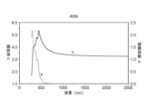
- FIG. 32 is a graph showing the wavelength dependence of the refractive index n and bandgap energy k of aluminum antimonide (AlSb).
- the refractive index n of AlSb for light with a wavelength of 500 nm is 4 or more, which is similar to that of Si (4 or more), and the bandgap energy k for light with a wavelength of 500 nm is that of Si (about 1.12 eV), which is about 1.58 eV.
- GaP As a constituent material of the in-pixel isolation section 170, the reflection at the interface between the semiconductor substrate 50 and the in-pixel isolation section 170 is suppressed, as in the above-described example. photoelectric conversion can be suppressed. Since AlSb is a group III-V semiconductor, it is possible to achieve low insulation.
- FIG. 33 is a graph showing wavelength dependence of refractive index n and bandgap energy k of indium phosphide (InP).
- the refractive index n of InP for light with a wavelength of 500 nm is 3.7, which is slightly lower than that of Si (4 or more), and the bandgap energy k for light with a wavelength of 500 nm is 3.7. It is about 1.29 eV, which is larger than that (about 1.12 eV).
- InP is a group III-V semiconductor, it is possible to achieve low insulation.
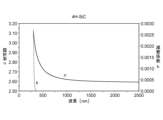
- FIG. 34 is a graph showing the wavelength dependence of refractive index n and bandgap energy k of hexagonal silicon carbide (4H—SiC).
- the refractive index n of 4H—SiC for light with a wavelength of 500 nm is 2.7, which is lower than that of Si (4 or more), but the bandgap energy k for light with a wavelength of 500 nm is It is about 3.26 eV, which is much larger than that (about 1.12 eV).
- 4H—SiC is a material having semiconductivity.
- hexagonal silicon carbide (6H-SiC) with a bandgap energy k of about 3.02 eV for light with a wavelength of 500 nm
- FIG. 35 is a graph showing the wavelength dependence of the refractive index n of diamond.
- the refractive index n of diamond for light with a wavelength of 500 nm is 2.4, which is lower than that of Si (4 or more), but the bandgap energy k for light with a wavelength of 500 nm is that of Si ( about 5.47 eV, which is much larger than about 1.12 eV).
- Diamond can be made conductive by doping it with an impurity such as boron (B).
- FIG. 36 is a graph showing wavelength dependence of refractive index n and bandgap energy k of DLC.
- the refractive index n of DLC for light with a wavelength of 500 nm is 2.01, which is lower than that of Si (4 or more), but the bandgap energy k for light with a wavelength of 500 nm is sp2/sp3
- the ratio it varies in the range of 0.8 eV to 4.0 eV, and the more sp3, the greater the bandgap energy k.
- DLC can be made conductive by doping it with an impurity such as boron (B).
- FIG. 37 is a graph showing wavelength dependence of refractive index n and bandgap energy k of zinc selenide (ZnSe).
- the refractive index n of ZnSe for light with a wavelength of 500 nm is 2.6, which is lower than that of Si (4 or more), but the bandgap energy k for light with a wavelength of 500 nm is that of Si ( about 2.7 eV, which is greater than about 1.12 eV).
- the pixel It is possible to greatly suppress the photoelectric conversion in the internal isolation portion 170 .
- ZnSe is an intrinsic semiconductor.
- AlSbAs aluminum antimonide arsenide
- AlSbP aluminum antimonide phosphide
- AlInP aluminum indium phosphide
- GaAsP gallium arsenide phosphide
- a ternary compound semiconductor such as indium gallium (InGaP) or gallium aluminum arsenide (GaAlAs) can be used as the material of the in-pixel isolation section 170 .
- the material for isolating pixels of the same color has the same or more (or less in some cases) material than the constituent material of the semiconductor substrate 58.
- a material that has a refractive index and a bandgap energy greater than that of the constituent material of the semiconductor substrate 58 a low refractive index (that is, a high reflectance) and a high reflectance can be obtained between pixels of different colors that are desired to be optically separated.
- High refractive index (i.e., low reflectance), high insulation, and non-photoelectric conversion characteristics were achieved between pixels of the same color for which it is desired to achieve electrical isolation without optical isolation while achieving insulation. It is possible to realize the solid-state imaging device 10 and electronic equipment.
- the case where the pixel separation unit 60 and the intra-pixel separation unit 170 are separately produced according to the characteristics required for each has been described as an example.
- the third embodiment by improving the performance of the intra-pixel separation unit, the decrease in the quantum efficiency Qs of the image plane phase difference pixel is suppressed, and the decrease in the light receiving sensitivity of the solid-state imaging device is suppressed. An example will be given.
- Japanese Unexamined Patent Application Publication No. 2018-201015 proposes a method of isolating the intra-pixel isolation part by embedding an oxide film or metal in order to improve the characteristics of the intra-pixel isolation part.
- Japanese Patent Application Laid-Open No. 2019-9425 proposes a method of controlling the characteristics of the intra-pixel separation portion by the impurity concentration under the same color pass.
- the manufacturing process of the intra-pixel isolation section becomes complicated, which increases the number of ion implantation processes into the photoelectric conversion layer, and there is concern about an increase in noise due to defect formation.
- the transfer efficiency and noise deteriorate as pixels become finer. Challenges also exist.
- the method disclosed in Japanese Patent Application Laid-Open No. 2019-9425 aims to optimize the potential structure between the left pixel and the right pixel by controlling the impurity concentration under the overflow path. It is considered that the process control for forming the intra-pixel isolation portion becomes difficult with the miniaturization of the pixel.
- the conventional method may have problems as exemplified below.
- the intra-pixel isolation is formed by a graded epitaxial (graded-epi) layer having a polarity opposite to the charge generated in the photoelectric conversion region, thereby forming an overflow path that electrically connects the left and right pixels.
- FIG. 38 is a top view showing a planar structure example of an image-plane phase difference pixel according to the present embodiment.
- FIG. 39 is a vertical cross-sectional view showing a structural example of the EE cross section in FIG.
- FIG. 40 is a vertical sectional view showing a structural example of the FF section in FIG.
- an intra-pixel separation unit 370 that divides an image plane phase difference pixel region partitioned by the pixel separation unit 60 into two, for example, rectangular regions is a first separation unit. 360 and a second separation section 371 .
- the first separating section 360 is, for example, a structural section continuing from the pixel separating section 60 and may have the same layer structure as the pixel separating section 69 .
- the second separation section 371 is arranged, for example, substantially in the center of the intra-pixel separation section 370 that separates the image plane phase difference pixel region so as to divide the first separation section 360 in the vertical direction.
- the impurity concentration of the second isolation section 371 in the region other than the overflow path 381 is, for example, directed toward the center of the second isolation section 371 in the horizontal direction.
- the polarity may be adjusted to be reversed as the distance from the overflow path 381 increases.
- the impurity concentration profile of the second isolation portion 371 is such that the potential barrier becomes higher toward the center of the second isolation portion 371 in the horizontal direction, and the potential barrier becomes higher away from the overflow path 381 in the vertical direction. may be adjusted to Also, in the region where the overflow path 381 is formed, the impurity concentration may be adjusted to be substantially uniform in the horizontal direction and the vertical direction.
- the second isolation portion 371 having such an impurity concentration profile may be configured using, for example, a graded-epi layer adjusted so that the impurity concentration increases toward the inside of the second isolation portion 371.
- this graded-epi layer may be a semiconductor layer (epitaxial layer) containing P-type impurities.
- a material having high potential energy for readout carriers may be used in relation to the constituent material of the photoelectric conversion portion PD.
- a group IV semiconductor composed of at least one of carbon (C), silicon (Si), germanium (Ge) and tin (Sn), boron (B), aluminum (Al), gallium (Ga), Group III-V semiconductors or the like composed of at least two of indium (In), nitrogen (N), phosphorus (P), arsenic (As) and antimony (Sb) may be used.
- C carbon
- Si silicon
- Ge germanium
- Sn boron
- Al aluminum
- Ga gallium
- Group III-V semiconductors or the like composed of at least two of indium (In), nitrogen (N), phosphorus (P), arsenic (As) and antimony (Sb)
- the transfer transistor 31 of each of the pixels 30A and 30B is provided, for example, at a corner where the pixel isolation portion 60 and the in-pixel isolation portion 370 intersect in each pixel region, and is provided on the surface of the semiconductor substrate 50 on the element forming surface side. and a gate insulating film 332 and a gate electrode 331 provided on the element forming surface.
- the other source/drain region of the transfer transistor 31 may be the cathode of the photoelectric conversion unit PD.
- this floating diffusion region FD is located at the corner where the pixel isolation portion 60 and the intra-pixel isolation portion 370 intersect, where the respective transfer transistors 31 are arranged. may be placed across the This floating diffusion region FD may be electrically connected to the diffusion regions 333 of the transfer transistors 31 of the pixels 30A and 30B through via contacts 334 .
- the above structure compared to the case where the left and right pixels are separated by ion implantation, it is possible to suppress defects in the vicinity of the region where the intra-pixel isolation portion 370 is formed, thereby suppressing noise. It becomes possible to In addition, since it becomes easier to control the width of the intra-pixel separation portion 370 in the horizontal direction (the direction parallel to the element forming surface), it is possible to suppress the reduction and variation in the saturation signal amount Qs. Furthermore, since the distance from the overflow path 381 (that is, the second isolation portion 371) to the transfer transistor 31 can be secured, the impurity concentration in the portion near the transfer transistor 31 can be kept low. As a result, it is possible to suppress deterioration of transfer efficiency and noise accompanying miniaturization.
- the intra-pixel separation section 370 (corresponding to the second separation section 371) is made of a semiconductor material, it is possible to suppress incident light from being blocked in the vicinity of the light collecting section and a decrease in photoelectric conversion efficiency. becomes possible.
- the transfer transistor 31 is the photoelectric conversion unit.
- the PD is arranged on the same light receiving chip 41
- at least one transistor other than the transfer transistor 31 may also be arranged on the light receiving chip 41 .
- 41 to 47 are process cross-sectional views showing the manufacturing method of the solid-state imaging device according to this embodiment.
- 41 to 47 (A) is a top view showing a planar structure example of the image plane phase difference pixel corresponding to FIG. 38, and (B) is an EE cross section corresponding to FIG. 41 is a vertical cross-sectional view showing a structural example of FIG. 40, and (C) is a vertical cross-sectional view showing a structural example of the FF cross section corresponding to FIG.
- the scale, size, etc. of each layer shown in FIGS. 41 to 47 are different from the scale, size, etc. of each layer shown in FIGS.
- a P-type dopant and an N-type dopant are appropriately ion-implanted into a prepared semiconductor substrate 58 to form a front surface side and a rear surface side of the semiconductor substrate 58.
- P-type semiconductor regions 56 and 64 are formed respectively, and an N-type semiconductor region 59 is formed in a region sandwiched between the P-type semiconductor regions 56 and 64 .
- a N A shallow trench (Shallow Trench Isolation: STI) T1 that exposes the upper layer of the semiconductor region 59 is formed.
- an insulating material is embedded in the trenches T1 formed on the front surface side of the semiconductor substrate 58, thereby filling the trenches T1 with an insulating material. Then, an insulating film 63A to be part of the insulating film 63 is formed.
- a region ie, A trench T2 deep enough to expose the P-type semiconductor region 64 on the back side of the semiconductor substrate 58 is formed in the region where the insulating film 63A is formed.
- anisotropic dry etching such as RIE (Reactive Ion Etching) may be used.
- a fixed charge film 62 is formed on the surface of the semiconductor substrate 58 exposed on the inner side surface and bottom surface of the trench T2.
- an insulating material is embedded in the trenches T2 in which the fixed charge films 62 are formed on the inner surface and the bottom surface.
- An insulating film 63 is formed in the trench T2. Thereby, the pixel separation portion 60 and the first separation portion 360 are formed.
- the P-type semiconductor region 64 on the rear surface side of the semiconductor substrate 58 is formed in the region where the second separation section 371 is formed on the front surface side of the semiconductor substrate 58 by using, for example, lithography.
- a trench T3 deep enough to expose the surface is formed.
- anisotropic dry etching such as RIE may be used.
- a film formation method such as an epitaxial growth technique (graded epitaxial technique) that can control the impurity concentration step by step, the opposite polarity becomes stronger as it goes inward.
- a second isolation portion 371 composed of a graded-epi layer with an adjusted impurity concentration is formed. At this time, the impurity concentration on the back surface side of the semiconductor substrate 58 in the second separation portion 371 is reduced, so that this region functions as the overflow path 381 .
- circuit elements such as the transfer transistor 31 and the wiring layer 65 are formed on the front side of the semiconductor substrate 58, and then the light shielding film 54, the planarization film 53, the color filter 52 and the on-chip lens 51 are formed on the back side of the semiconductor substrate 58. are sequentially formed, the solid-state imaging device 10 having the image plane phase difference pixels having the cross-sectional structures shown in FIGS. 38 to 40 can be manufactured.
- FIG. 48 is a vertical cross-sectional view showing a cross-sectional structure example of an image plane phase difference pixel according to a first modification.
- the fixed charge film 62 in the pixel separation section 60 is formed in a diffusion region 62a formed by injecting ions having a polarity opposite to that of charges generated in the photoelectric conversion section PD. has been replaced.
- the potential around the photoelectric conversion unit PD can also be adjusted by using the diffusion region 62a formed by ion implantation, solid phase diffusion, or the like instead of the fixed charge film 62 formed using PLAD, for example. Is possible.
- FIG. 49 is a vertical sectional view showing a cross-sectional structure example of an image plane phase difference pixel according to a second modification.
- a pixel separation section 60 with an RDTI structure is used instead of the pixel separation section 60 with an FTI structure.
- the pixel isolation part 60 of the RDTI structure has a structure in which a trench carved from the rear surface (light incident surface) side of the semiconductor substrate 58 is filled with an insulating film 63b, and the periphery of the insulating film 63b is covered with a fixed charge film 62b.
- the structure of the pixel separation section 60 (and the first separation section 360) that optically and electrically separates the image plane phase difference pixel regions (and part of the pixel regions) is an FTI structure or an RDTI structure. etc., various structures may be adopted.
- FIG. 50 is a vertical sectional view showing a cross-sectional structure example of an image plane phase difference pixel according to a third modification.
- the pixel separation section 60 with the RDTI structure is used instead of the pixel separation section 60 with the FTI structure.
- the fixed charge film 62b covering the insulating film 63b is formed by ion implantation or replaced with a diffusion region 62c, and a diffusion region is formed between the upper surface of the insulating film 63b and the P-type semiconductor region 56. 68c is arranged.
- the diffusion region 68c electrically closes the space from the upper surface of the insulating film 63b to the P-type semiconductor region 56, thereby enabling the adjacent image plane phase difference pixels to be separated from each other. It is possible to increase the electrical isolation between
- the dopant contained in the diffusion region 68c may be the same as that in the diffusion region 63a. Diffusion region 68c and diffusion region 63a may be formed in the same ion implantation process or may be formed in separate ion implantation processes.
- FIG. 51 is a vertical sectional view showing a cross-sectional structure example of an image plane phase difference pixel according to a fourth modification.
- the pixel separation portion 60 having a physical structure is formed by implanting ions having a polarity opposite to that of charges generated in the photoelectric conversion portion PD into the semiconductor substrate 58. is replaced by the diffused region 60d.
- the separation structure between the image plane phase difference pixel regions (and part of the pixel regions) is not limited to a physical structure, and may be variously modified such as a separation structure based on a potential structure.
- FIG. 52 is a vertical cross-sectional view showing a cross-sectional structure example of an image plane phase difference pixel according to a fifth modification.
- the fifth modification at least the second separation section 371 in the intra-pixel separation section 370 separating the image plane phase difference pixel regions separated by the pixel separation section 60 is the second separation section 371 having the RDTI structure. It is replaced by the separating part 372 .
- the overflow path 382 is formed on the front surface side (element forming surface side) of the semiconductor substrate 58 .
- the second separating section 372 that partitions adjacent pixels while having an overflow path is not limited to the FTI structure, and various modifications are possible.
- the formation position of the overflow path is not limited to the back surface side of the semiconductor substrate 58, and can be variously changed to the front surface side of the semiconductor substrate 58, an intermediate portion, or the like.
- the second isolation portion 372 of the RDTI structure is formed by graded-layer deposition from the back surface side of the semiconductor substrate 58 using a film forming method such as an epitaxial growth technique (Graded Epitaxial Technique) capable of stepwise control of the impurity concentration. It can be formed by forming an epi layer.
- a film forming method such as an epitaxial growth technique (Graded Epitaxial Technique) capable of stepwise control of the impurity concentration. It can be formed by forming an epi layer.
- FIG. 53 is a vertical sectional view showing a cross-sectional structure example of an image plane phase difference pixel according to a sixth modification.
- a plurality of overflow paths connecting adjacent pixels are provided in the sixth modification.
- FIG. 53 illustrates a case where overflow paths 383a and 383b are formed at two locations in the substrate thickness direction of the semiconductor substrate 58.
- the number of overflow paths through which charges overflowing from one pixel 30 flow is not limited to one, and a plurality of paths may be provided.
- the charge overflowing from one pixel 30 efficiently flows into the other pixel 30, so that the difference in light-receiving sensitivity between the two pixels can be further reduced.
- the positions where the plurality of overflow paths 383a and 383b are formed are not limited to the intermediate portion of the semiconductor substrate 58, and may be on the front surface side or the rear surface side.
- the second isolation section 373 having a plurality of overflow paths 383a and 383b divides the film formation process into a plurality of stages using a film formation method such as an epitaxial growth technique capable of stepwise controlling the impurity concentration. may be formed by executing
- FIG. 54 is a vertical sectional view showing a cross-sectional structure example of an image plane phase difference pixel according to a seventh modification.
- an intra-pixel separating section 370 including a first separating section 360, a second separating section 371, and the like is replaced with an intra-pixel separating section 374 entirely formed of a graded-epi layer.
- at least one of the upper layer portion, the lower layer portion, and the intermediate portion of the intra-pixel isolation portion 374 functions as an overflow path as a whole along the element formation surface of the semiconductor substrate 58.
- the charge overflowing from one pixel 30 efficiently flows into the other pixel 30, so that the difference in light-receiving sensitivity between the two pixels can be further reduced. .
- FIG. 55 is a vertical sectional view showing a cross-sectional structure example of an image plane phase difference pixel according to an eighth modification.
- the second separation section 371 in the intra-pixel separation section 370 electrically separates adjacent pixels by utilizing the difference in electron energy levels between substances (band offset). It is replaced with a second separating portion 375 that separates into .
- the band offset of the second isolation part 371 can be realized by, for example, the doping density of impurities, the material composition, and the like. In this way, even when the adjacent pixels are electrically separated by using the band offset, by configuring a portion thereof to function as the overflow path 385, the difference in photosensitivity between the adjacent pixels can be reduced. becomes possible.
- the structural examples of the image plane phase difference pixels exemplified in the third embodiment and the structural examples of the image plane phase difference pixels exemplified in the first modification to the eighth modification can be appropriately combined.
- the fifth modification to the eighth modification By combining one or more of the structural examples of the image plane phase difference pixels exemplified in the modified examples, it is possible to obtain the effect of each of the structural examples used in the combination.
- the in-pixel separation section 370 is a film (for example, a graded -epi layer), noise caused by defects near the separation region can be reduced compared to the case where intra-pixel separation is performed in the diffusion region.
- a physical isolation structure it is possible to easily control the width of the intra-pixel isolation in the horizontal direction.
- the overflow path 371 and the like can be separated from the transfer transistor 31, and the impurity concentration in the portion near the transfer transistor 31 can be kept low, deterioration of transfer efficiency and noise accompanying miniaturization can be suppressed.
- the intra-pixel separation section 370 is formed of a semiconductor, it is possible to suppress the rejection of incident light and the reduction of the photoelectric conversion area.
- FIG. 56 is a block diagram showing an example of a schematic functional configuration of a smart phone 900 to which the technology according to the present disclosure (this technology) can be applied.
- a smartphone 900 includes a CPU (Central Processing Unit) 901, a ROM (Read Only Memory) 902, and a RAM (Random Access Memory) 903.
- Smartphone 900 also includes storage device 904 , communication module 905 , and sensor module 907 .
- smart phone 900 includes imaging device 1 , display device 910 , speaker 911 , microphone 912 , input device 913 and bus 914 .
- the smartphone 900 may have a processing circuit such as a DSP (Digital Signal Processor) in place of the CPU 901 or together with it.
- DSP Digital Signal Processor
- the CPU 901 functions as an arithmetic processing device and a control device, and controls all or part of the operations within the smartphone 900 according to various programs recorded in the ROM 902, RAM 903, storage device 904, or the like.
- a ROM 902 stores programs and calculation parameters used by the CPU 901 .
- the RAM 903 temporarily stores programs used in the execution of the CPU 901, parameters that change as appropriate during the execution, and the like.
- the CPU 901 , ROM 902 and RAM 903 are interconnected by a bus 914 .
- the storage device 904 is a data storage device configured as an example of a storage unit of the smartphone 900 .
- the storage device 904 is composed of, for example, a magnetic storage device such as a HDD (Hard Disk Drive), a semiconductor storage device, an optical storage device, or the like.
- the storage device 904 stores programs executed by the CPU 901, various data, and various data acquired from the outside.
- the communication module 905 is, for example, a communication interface configured with a communication device for connecting to the communication network 906.
- the communication module 905 can be, for example, a communication card for wired or wireless LAN (Local Area Network), Bluetooth (registered trademark), or WUSB (Wireless USB).
- the communication module 905 may be a router for optical communication, a router for ADSL (Asymmetric Digital Subscriber Line), a modem for various types of communication, or the like.
- a communication network 906 connected to the communication module 905 is a wired or wireless network, such as the Internet, home LAN, infrared communication, or satellite communication.
- the sensor module 907 is, for example, a motion sensor (eg, an acceleration sensor, a gyro sensor, a geomagnetic sensor, etc.), a biological information sensor (eg, a pulse sensor, a blood pressure sensor, a fingerprint sensor, etc.), or a position sensor (eg, GNSS (Global Navigation Satellite system) receiver, etc.) and various sensors.
- a motion sensor eg, an acceleration sensor, a gyro sensor, a geomagnetic sensor, etc.
- a biological information sensor eg, a pulse sensor, a blood pressure sensor, a fingerprint sensor, etc.
- GNSS Global Navigation Satellite system
- the imaging device 1 is provided on the surface of the smartphone 900 and can image an object or the like located on the back side or the front side of the smartphone 900 .
- the imaging device 1 includes an imaging device (not shown) such as a CMOS (Complementary MOS) image sensor to which the technology according to the present disclosure (this technology) can be applied, and a signal photoelectrically converted by the imaging device. and a signal processing circuit (not shown) that performs imaging signal processing.
- the imaging device 1 further includes an optical system mechanism (not shown) composed of an imaging lens, a zoom lens, a focus lens, etc., and a drive system mechanism (not shown) for controlling the operation of the optical system mechanism. can be done.
- the image sensor collects incident light from an object as an optical image
- the signal processing circuit photoelectrically converts the formed optical image pixel by pixel, and reads the signal of each pixel as an image signal. , a captured image can be acquired by performing image processing.
- the display device 910 is provided on the surface of the smartphone 900 and can be, for example, a display device such as an LCD (Liquid Crystal Display) or an organic EL (Electro Luminescence) display.
- the display device 910 can display an operation screen, captured images acquired by the imaging device 1 described above, and the like.
- the speaker 911 can output, for example, the voice of a call, the voice accompanying the video content displayed by the display device 910 described above, and the like to the user.
- the microphone 912 can collect, for example, the user's call voice, voice including commands for activating functions of the smartphone 900 , and ambient environment voice of the smartphone 900 .
- the input device 913 is, for example, a device operated by a user, such as a button, keyboard, touch panel, or mouse.
- the input device 913 includes an input control circuit that generates an input signal based on information input by the user and outputs the signal to the CPU 901 .
- the user can input various data to the smartphone 900 and instruct processing operations.
- a configuration example of the smartphone 900 has been shown above.
- Each component described above may be configured using general-purpose members, or may be configured by hardware specialized for the function of each component. Such a configuration can be changed as appropriate according to the technical level of implementation.
- the technology according to the present disclosure can be applied to various products.
- the technology according to the present disclosure can be realized as a device mounted on any type of moving body such as automobiles, electric vehicles, hybrid electric vehicles, motorcycles, bicycles, personal mobility, airplanes, drones, ships, and robots. may
- FIG. 57 is a block diagram showing a schematic configuration example of a vehicle control system, which is an example of a mobile control system to which the technology according to the present disclosure can be applied.
- a vehicle control system 12000 includes a plurality of electronic control units connected via a communication network 12001.
- the vehicle control system 12000 includes a driving system control unit 12010, a body system control unit 12020, a vehicle exterior information detection unit 12030, a vehicle interior information detection unit 12040, and an integrated control unit 12050.
- a microcomputer 12051, an audio/image output unit 12052, and an in-vehicle network I/F (Interface) 12053 are illustrated.
- the drive system control unit 12010 controls the operation of devices related to the drive system of the vehicle according to various programs.
- the driving system control unit 12010 includes a driving force generator for generating driving force of the vehicle such as an internal combustion engine or a driving motor, a driving force transmission mechanism for transmitting the driving force to the wheels, and a steering angle of the vehicle. It functions as a control device such as a steering mechanism to adjust and a brake device to generate braking force of the vehicle.
- the body system control unit 12020 controls the operation of various devices equipped on the vehicle body according to various programs.
- the body system control unit 12020 functions as a keyless entry system, a smart key system, a power window device, or a control device for various lamps such as headlamps, back lamps, brake lamps, winkers or fog lamps.
- body system control unit 12020 can receive radio waves transmitted from a portable device that substitutes for a key or signals from various switches.
- the body system control unit 12020 receives the input of these radio waves or signals and controls the door lock device, power window device, lamps, etc. of the vehicle.
- the vehicle exterior information detection unit 12030 detects information outside the vehicle in which the vehicle control system 12000 is installed.
- the vehicle exterior information detection unit 12030 is connected with an imaging section 12031 .
- the vehicle exterior information detection unit 12030 causes the imaging unit 12031 to capture an image of the exterior of the vehicle, and receives the captured image.
- the vehicle exterior information detection unit 12030 may perform object detection processing or distance detection processing such as people, vehicles, obstacles, signs, or characters on the road surface based on the received image.
- the imaging unit 12031 is an optical sensor that receives light and outputs an electrical signal according to the amount of received light.
- the imaging unit 12031 can output the electric signal as an image, and can also output it as distance measurement information.
- the light received by the imaging unit 12031 may be visible light or non-visible light such as infrared rays.
- the in-vehicle information detection unit 12040 detects in-vehicle information.
- the in-vehicle information detection unit 12040 is connected to, for example, a driver state detection section 12041 that detects the state of the driver.
- the driver state detection unit 12041 includes, for example, a camera that captures an image of the driver, and the in-vehicle information detection unit 12040 detects the degree of fatigue or concentration of the driver based on the detection information input from the driver state detection unit 12041. It may be calculated, or it may be determined whether the driver is dozing off.
- the microcomputer 12051 calculates control target values for the driving force generator, the steering mechanism, or the braking device based on the information inside and outside the vehicle acquired by the vehicle exterior information detection unit 12030 or the vehicle interior information detection unit 12040, and controls the drive system control unit.
- a control command can be output to 12010 .
- the microcomputer 12051 realizes ADAS (Advanced Driver Assistance System) functions including collision avoidance or shock mitigation, follow-up driving based on inter-vehicle distance, vehicle speed maintenance driving, vehicle collision warning, or vehicle lane deviation warning. Cooperative control can be performed for the purpose of ADAS (Advanced Driver Assistance System) functions including collision avoidance or shock mitigation, follow-up driving based on inter-vehicle distance, vehicle speed maintenance driving, vehicle collision warning, or vehicle lane deviation warning. Cooperative control can be performed for the purpose of ADAS (Advanced Driver Assistance System) functions including collision avoidance or shock mitigation, follow-up driving based on inter-vehicle distance, vehicle speed maintenance driving, vehicle collision warning, or vehicle
- the microcomputer 12051 controls the driving force generator, the steering mechanism, the braking device, etc. based on the information about the vehicle surroundings acquired by the vehicle exterior information detection unit 12030 or the vehicle interior information detection unit 12040, so that the driver's Cooperative control can be performed for the purpose of autonomous driving, etc., in which vehicles autonomously travel without depending on operation.
- the microcomputer 12051 can output a control command to the body system control unit 12020 based on the information outside the vehicle acquired by the information detection unit 12030 outside the vehicle.
- the microcomputer 12051 controls the headlamps according to the position of the preceding vehicle or the oncoming vehicle detected by the vehicle exterior information detection unit 12030, and performs cooperative control aimed at anti-glare such as switching from high beam to low beam. It can be carried out.
- the audio/image output unit 12052 transmits at least one of audio and/or image output signals to an output device capable of visually or audibly notifying the passengers of the vehicle or the outside of the vehicle.
- an audio speaker 12061, a display unit 12062 and an instrument panel 12063 are illustrated as output devices.
- the display unit 12062 may include at least one of an on-board display and a head-up display, for example.
- FIG. 58 is a diagram showing an example of the installation position of the imaging unit 12031.
- the imaging unit 12031 has imaging units 12101, 12102, 12103, 12104, and 12105.
- the imaging units 12101, 12102, 12103, 12104, and 12105 are provided at positions such as the front nose, side mirrors, rear bumper, back door, and windshield of the vehicle 12100, for example.
- An image pickup unit 12101 provided in the front nose and an image pickup unit 12105 provided above the windshield in the passenger compartment mainly acquire images in front of the vehicle 12100 .
- Imaging units 12102 and 12103 provided in the side mirrors mainly acquire side images of the vehicle 12100 .
- An imaging unit 12104 provided in the rear bumper or back door mainly acquires an image behind the vehicle 12100 .
- the imaging unit 12105 provided above the windshield in the passenger compartment is mainly used for detecting preceding vehicles, pedestrians, obstacles, traffic lights, traffic signs, lanes, and the like.
- FIG. 58 shows an example of the imaging range of the imaging units 12101 to 12104.
- FIG. The imaging range 12111 indicates the imaging range of the imaging unit 12101 provided in the front nose
- the imaging ranges 12112 and 12113 indicate the imaging ranges of the imaging units 12102 and 12103 provided in the side mirrors, respectively
- the imaging range 12114 The imaging range of an imaging unit 12104 provided in the rear bumper or back door is shown. For example, by superimposing the image data captured by the imaging units 12101 to 12104, a bird's-eye view image of the vehicle 12100 viewed from above can be obtained.
- At least one of the imaging units 12101 to 12104 may have a function of acquiring distance information.
- at least one of the imaging units 12101 to 12104 may be a stereo camera composed of a plurality of imaging elements, or may be an imaging element having pixels for phase difference detection.
- the microcomputer 12051 determines the distance to each three-dimensional object within the imaging ranges 12111 to 12114 and changes in this distance over time (relative velocity with respect to the vehicle 12100). , it is possible to extract, as the preceding vehicle, the closest three-dimensional object on the traveling path of the vehicle 12100, which runs at a predetermined speed (for example, 0 km/h or more) in substantially the same direction as the vehicle 12100. can. Furthermore, the microcomputer 12051 can set the inter-vehicle distance to be secured in advance in front of the preceding vehicle, and perform automatic brake control (including following stop control) and automatic acceleration control (including following start control). In this way, cooperative control can be performed for the purpose of automatic driving in which the vehicle runs autonomously without relying on the operation of the driver.
- automatic brake control including following stop control
- automatic acceleration control including following start control
- the microcomputer 12051 converts three-dimensional object data related to three-dimensional objects to other three-dimensional objects such as motorcycles, ordinary vehicles, large vehicles, pedestrians, and utility poles. It can be classified and extracted and used for automatic avoidance of obstacles. For example, the microcomputer 12051 distinguishes obstacles around the vehicle 12100 into those that are visible to the driver of the vehicle 12100 and those that are difficult to see. Then, the microcomputer 12051 judges the collision risk indicating the degree of danger of collision with each obstacle, and when the collision risk is equal to or higher than the set value and there is a possibility of collision, an audio speaker 12061 and a display unit 12062 are displayed. By outputting an alarm to the driver via the drive system control unit 12010 and performing forced deceleration and avoidance steering via the drive system control unit 12010, driving support for collision avoidance can be performed.
- At least one of the imaging units 12101 to 12104 may be an infrared camera that detects infrared rays.
- the microcomputer 12051 can recognize a pedestrian by determining whether or not the pedestrian exists in the captured images of the imaging units 12101 to 12104 .
- recognition of a pedestrian is performed by, for example, a procedure for extracting feature points in images captured by the imaging units 12101 to 12104 as infrared cameras, and performing pattern matching processing on a series of feature points indicating the outline of an object to determine whether or not the pedestrian is a pedestrian.
- the audio image output unit 12052 outputs a rectangular outline for emphasis to the recognized pedestrian. is superimposed on the display unit 12062 . Also, the audio/image output unit 12052 may control the display unit 12062 to display an icon or the like indicating a pedestrian at a desired position.
- the technology according to the present disclosure can be applied to the imaging unit 12031 and the like among the configurations described above.
- By applying the technology according to the present disclosure to the imaging unit 12031 it is possible to obtain a captured image that is easier to see, thereby reducing driver fatigue.
- FIG. 59 is a diagram showing an example of a schematic configuration of an endoscopic surgery system to which the technology according to the present disclosure (this technology) can be applied.
- FIG. 59 illustrates a state in which an operator (doctor) 11131 is performing surgery on a patient 11132 on a patient bed 11133 using an endoscopic surgery system 11000 .
- an endoscopic surgery system 11000 includes an endoscope 11100, other surgical instruments 11110 such as a pneumoperitoneum tube 11111 and an energy treatment instrument 11112, and a support arm device 11120 for supporting the endoscope 11100. , and a cart 11200 loaded with various devices for endoscopic surgery.
- An endoscope 11100 is composed of a lens barrel 11101 whose distal end is inserted into the body cavity of a patient 11132 and a camera head 11102 connected to the proximal end of the lens barrel 11101 .
- an endoscope 11100 configured as a so-called rigid scope having a rigid lens barrel 11101 is illustrated, but the endoscope 11100 may be configured as a so-called flexible scope having a flexible lens barrel. good.
- the tip of the lens barrel 11101 is provided with an opening into which the objective lens is fitted.
- a light source device 11203 is connected to the endoscope 11100, and light generated by the light source device 11203 is guided to the tip of the lens barrel 11101 by a light guide extending inside the lens barrel 11101, where it reaches the objective. Through the lens, the light is irradiated toward the observation object inside the body cavity of the patient 11132 .
- the endoscope 11100 may be a straight scope, a perspective scope, or a side scope.
- An optical system and an imaging element are provided inside the camera head 11102, and the reflected light (observation light) from the observation target is focused on the imaging element by the optical system.
- the imaging device photoelectrically converts the observation light to generate an electrical signal corresponding to the observation light, that is, an image signal corresponding to the observation image.
- the image signal is transmitted to a camera control unit (CCU: Camera Control Unit) 11201 as RAW data.
- CCU Camera Control Unit
- the CCU 11201 is composed of a CPU (Central Processing Unit), a GPU (Graphics Processing Unit), etc., and controls the operations of the endoscope 11100 and the display device 11202 in an integrated manner. Further, the CCU 11201 receives an image signal from the camera head 11102 and performs various image processing such as development processing (demosaicing) for displaying an image based on the image signal.
- CPU Central Processing Unit
- GPU Graphics Processing Unit
- the display device 11202 displays an image based on an image signal subjected to image processing by the CCU 11201 under the control of the CCU 11201 .
- the light source device 11203 is composed of a light source such as an LED (light emitting diode), for example, and supplies the endoscope 11100 with irradiation light for imaging a surgical site or the like.
- a light source such as an LED (light emitting diode)
- LED light emitting diode
- the input device 11204 is an input interface for the endoscopic surgery system 11000.
- the user can input various information and instructions to the endoscopic surgery system 11000 via the input device 11204 .
- the user inputs an instruction or the like to change the imaging conditions (type of irradiation light, magnification, focal length, etc.) by the endoscope 11100 .
- the treatment instrument control device 11205 controls driving of the energy treatment instrument 11112 for tissue cauterization, incision, blood vessel sealing, or the like.
- the pneumoperitoneum device 11206 inflates the body cavity of the patient 11132 for the purpose of securing the visual field of the endoscope 11100 and securing the operator's working space, and injects gas into the body cavity through the pneumoperitoneum tube 11111. send in.
- the recorder 11207 is a device capable of recording various types of information regarding surgery.
- the printer 11208 is a device capable of printing various types of information regarding surgery in various formats such as text, images, and graphs.
- the light source device 11203 that supplies the endoscope 11100 with irradiation light for photographing the surgical site can be composed of, for example, a white light source composed of an LED, a laser light source, or a combination thereof.
- a white light source is configured by a combination of RGB laser light sources
- the output intensity and output timing of each color (each wavelength) can be controlled with high accuracy. It can be carried out.
- the observation target is irradiated with laser light from each of the RGB laser light sources in a time division manner, and by controlling the drive of the imaging device of the camera head 11102 in synchronization with the irradiation timing, each of RGB can be handled. It is also possible to pick up images by time division. According to this method, a color image can be obtained without providing a color filter in the imaging device.
- the driving of the light source device 11203 may be controlled so as to change the intensity of the output light every predetermined time.
- the drive of the imaging device of the camera head 11102 in synchronism with the timing of the change in the intensity of the light to obtain an image in a time-division manner and synthesizing the images, a high dynamic A range of images can be generated.
- the light source device 11203 may be configured to be able to supply light in a predetermined wavelength band corresponding to special light observation.
- special light observation for example, by utilizing the wavelength dependence of light absorption in body tissues, by irradiating light with a narrower band than the irradiation light (i.e., white light) during normal observation, the mucosal surface layer So-called Narrow Band Imaging, in which a predetermined tissue such as a blood vessel is imaged with high contrast, is performed.
- fluorescence observation may be performed in which an image is obtained from fluorescence generated by irradiation with excitation light.
- the body tissue is irradiated with excitation light and the fluorescence from the body tissue is observed (autofluorescence observation), or a reagent such as indocyanine green (ICG) is locally injected into the body tissue and the body tissue is examined.
- a fluorescence image can be obtained by irradiating excitation light corresponding to the fluorescence wavelength of the reagent.
- the light source device 11203 can be configured to be able to supply narrowband light and/or excitation light corresponding to such special light observation.
- FIG. 60 is a block diagram showing an example of functional configurations of the camera head 11102 and CCU 11201 shown in FIG.
- the camera head 11102 has a lens unit 11401, an imaging section 11402, a drive section 11403, a communication section 11404, and a camera head control section 11405.
- the CCU 11201 has a communication section 11411 , an image processing section 11412 and a control section 11413 .
- the camera head 11102 and the CCU 11201 are communicably connected to each other via a transmission cable 11400 .
- a lens unit 11401 is an optical system provided at a connection with the lens barrel 11101 . Observation light captured from the tip of the lens barrel 11101 is guided to the camera head 11102 and enters the lens unit 11401 .
- a lens unit 11401 is configured by combining a plurality of lenses including a zoom lens and a focus lens.
- the number of imaging elements constituting the imaging unit 11402 may be one (so-called single-plate type) or plural (so-called multi-plate type).
- image signals corresponding to RGB may be generated by each image pickup element, and a color image may be obtained by synthesizing the image signals.
- the imaging unit 11402 may be configured to have a pair of imaging elements for respectively acquiring right-eye and left-eye image signals corresponding to 3D (dimensional) display.
- the 3D display enables the operator 11131 to more accurately grasp the depth of the living tissue in the surgical site.
- a plurality of systems of lens units 11401 may be provided corresponding to each imaging element.
- the imaging unit 11402 does not necessarily have to be provided in the camera head 11102 .
- the imaging unit 11402 may be provided inside the lens barrel 11101 immediately after the objective lens.
- the drive unit 11403 is configured by an actuator, and moves the zoom lens and focus lens of the lens unit 11401 by a predetermined distance along the optical axis under control from the camera head control unit 11405 . Thereby, the magnification and focus of the image captured by the imaging unit 11402 can be appropriately adjusted.
- the communication unit 11404 is composed of a communication device for transmitting and receiving various information to and from the CCU 11201.
- the communication unit 11404 transmits the image signal obtained from the imaging unit 11402 as RAW data to the CCU 11201 via the transmission cable 11400 .
- the communication unit 11404 receives a control signal for controlling driving of the camera head 11102 from the CCU 11201 and supplies it to the camera head control unit 11405 .
- the control signal includes, for example, information to specify the frame rate of the captured image, information to specify the exposure value at the time of imaging, and/or information to specify the magnification and focus of the captured image. Contains information about conditions.
- the imaging conditions such as the frame rate, exposure value, magnification, and focus may be appropriately designated by the user, or may be automatically set by the control unit 11413 of the CCU 11201 based on the acquired image signal. good.
- the endoscope 11100 is equipped with so-called AE (Auto Exposure) function, AF (Auto Focus) function and AWB (Auto White Balance) function.
- the camera head control unit 11405 controls driving of the camera head 11102 based on the control signal from the CCU 11201 received via the communication unit 11404.
- the communication unit 11411 is composed of a communication device for transmitting and receiving various information to and from the camera head 11102 .
- the communication unit 11411 receives image signals transmitted from the camera head 11102 via the transmission cable 11400 .
- the communication unit 11411 transmits a control signal for controlling driving of the camera head 11102 to the camera head 11102 .
- Image signals and control signals can be transmitted by electrical communication, optical communication, or the like.
- the image processing unit 11412 performs various types of image processing on the image signal, which is RAW data transmitted from the camera head 11102 .
- the control unit 11413 performs various controls related to imaging of the surgical site and the like by the endoscope 11100 and display of the captured image obtained by imaging the surgical site and the like. For example, the control unit 11413 generates control signals for controlling driving of the camera head 11102 .
- control unit 11413 causes the display device 11202 to display a captured image showing the surgical site and the like based on the image signal that has undergone image processing by the image processing unit 11412 .
- the control unit 11413 may recognize various objects in the captured image using various image recognition techniques. For example, the control unit 11413 detects the shape, color, and the like of the edges of objects included in the captured image, thereby detecting surgical instruments such as forceps, specific body parts, bleeding, mist during use of the energy treatment instrument 11112, and the like. can recognize.
- the control unit 11413 may use the recognition result to display various types of surgical assistance information superimposed on the image of the surgical site. By superimposing and presenting the surgery support information to the operator 11131, the burden on the operator 11131 can be reduced and the operator 11131 can proceed with the surgery reliably.
- a transmission cable 11400 connecting the camera head 11102 and the CCU 11201 is an electrical signal cable compatible with electrical signal communication, an optical fiber compatible with optical communication, or a composite cable of these.
- wired communication is performed using the transmission cable 11400, but communication between the camera head 11102 and the CCU 11201 may be performed wirelessly.
- the technology according to the present disclosure can be applied to, for example, the imaging unit 11402 of the camera head 11102 among the configurations described above.
- the technology according to the present disclosure can be applied to the camera head 11102, a clearer image of the surgical site can be obtained, so that the operator can reliably confirm the surgical site.
- the technology according to the present disclosure may also be applied to, for example, a microsurgery system.
- the present technology can also take the following configuration.
- the etching stopper region is a partial region of the semiconductor substrate.
- the in-pixel separation portion extends from the first surface of the semiconductor substrate toward a second surface opposite to the first surface and does not reach the second surface. ).
- the intra-pixel separation section is made of diamond, DLC (Diamond-like Carbon), titanium oxide (TiO 2 ), cerium oxide (CeO 2 ), iron oxide (Fe 2 O 3 ), silicon nitride (SiN), gallium arsenide ( GaAs), gallium phosphide (GaP), aluminum arsenide (AlAs), aluminum antimonide (AlSb), indium phosphide (InP), hexagonal silicon carbide (4H-SiC), hexagonal silicon carbide (6H-SiC) , cubic silicon carbide (3C—SiC), zinc selenide (ZnSe), aluminum antimonide arsenide (AlSbAs), aluminum antimonide phosphide (AlSbP), aluminum indium phosphide (AlInP), gallium arsenide phosphide (GaAsP) ), indium gallium phosphide (InGaP), and gallium aluminum arsenide (G
- the solid-state imaging device according to any one of (1) to (5), wherein the pixel separation section includes at least one of silicon oxide (SiO 2 ), tungsten (W), and aluminum (Al).
- the in-pixel isolation part has a shape in which the width of the top surface located on the side of the second surface opposite to the first surface of the semiconductor substrate is narrower than the width of the bottom surface located on the side of the first surface. ) to (6).
- the pixel separation section optically and electrically separates the first regions, The solid-state imaging device according to any one of (1) to (7), wherein the intra-pixel isolation section electrically isolates the at least two second regions.
- the solid-state imaging device according to any one of (1) to (8), wherein the pixel separation section is arranged on a surface in contact with the semiconductor substrate and includes a fixed charge film having a negative fixed charge.
- the fixed charge film includes at least one of oxides of hafnium, zirconium, aluminum, tantalum, titanium, magnesium, yttrium, and lanthanide elements.
- a pixel separation section that partitions a first surface of a semiconductor substrate into a plurality of first regions arranged in a matrix; In a pixel comprising: dividing each of said first regions into at least two second regions, and an overflow path region for charge accumulated in one of said at least two second regions to flow into at least one of the other a separation unit; a photoelectric conversion unit arranged in each of the second regions; a transfer transistor connected to each of the photoelectric conversion units; with At least a part of the intra-pixel separating section has a potential barrier that increases toward the center of the intra-pixel separating section in a plane parallel to the first plane, and increases away from the overflow path.
- a solid-state imaging device having an adjusted impurity concentration profile.
- the solid-state imaging device according to any one of (11) to (14), wherein the impurities are impurities having high potential energy with respect to charges generated in the photoelectric conversion section.
- At least a part of the intra-pixel separation section is a semiconductor layer containing impurities having a polarity opposite to the polarity of the impurities contained in the semiconductor substrate.
- At least a part of the intra-pixel isolation part is a group IV semiconductor composed of at least one of carbon (C), silicon (Si), germanium (Ge) and tin (Sn), and boron (B).
- the solid-state imaging device according to any one of (11) to (16) above, including at least one of (18) The solid-state imaging device according to any one of (11) to (16), wherein the potential barrier is formed by a band offset. (19) The solid-state imaging device according to any one of (11) to (18), wherein at least another part of the intra-pixel separation section has the same layer structure as that of the pixel separation section. (20) the solid-state imaging device according to any one of (1) to (19); a processor that performs predetermined processing on image data output from the solid-state imaging device; electronic equipment.
Landscapes
- Engineering & Computer Science (AREA)
- Multimedia (AREA)
- Signal Processing (AREA)
- Solid State Image Pick-Up Elements (AREA)
Abstract
Description
1.第1の実施形態
1.1 電子機器(撮像装置)の構成例
1.2 固体撮像装置の構成例
1.3 画素の構成例
1.4 画素の基本機能例
1.5 固体撮像装置の積層構造例
1.6 画素の基本構造例
1.7 像面位相差画素の概略断面構造例
1.8 像面位相差画素構造における課題
1.9 像面位相差画素の断面構造例
1.10 製造方法
1.11 まとめ
1.12 変形例
1.12.1 第1の変形例
1.12.2 第2の変形例
1.12.3 第3の変形例
1.12.4 第4の変形例
1.12.5 第5の変形例
1.12.6 第6の変形例
2.第2の実施形態
2.1 第1例
2.2 第2例
2.3 第3例
2.4 第4例
2.5 第5例
2.6 第6例
2.7 第7例
2.8 第8例
2.9 第9例
2.10 その他の例
2.11 まとめ
3.第3の実施形態
3.1 像面位相差画素の断面構造例
3.2 製造方法
3.3 像面位相差画素構造の変形例
3.3.1 第1変形例
3.3.2 第2変形例
3.3.3 第3変形例
3.3.4 第4変形例
3.3.5 第5変形例
3.3.6 第6変形例
3.3.7 第7変形例
3.3.8 第8変形例
3.4 まとめ
4.スマートフォンへの応用例
5.移動体への応用例
6.内視鏡手術システムへの応用例
まず、本開示の第1の実施形態について、図面を参照して詳細に説明する。なお、本実施形態では、CMOS(Complementary Metal-Oxide-Semiconductor)型の固体撮像装置(以下、イメージセンサともいう)に本実施形態に係る技術を適用した場合を例示するが、これに限定されず、例えば、CCD(Charge Coupled Device)型の固体撮像装置やToF(Time of Flight)センサやEVS(Event-based Vision Sensor)など、光電変換素子を備える種々のセンサに本実施形態に係る技術を適用することが可能である。
図1は、第1の実施形態に係る固体撮像装置を搭載した電子機器(撮像装置)の概略構成例を示すブロック図である。図1に示すように、撮像装置1は、例えば、撮像レンズ11と、固体撮像装置10と、記憶部14と、プロセッサ13とを備える。
図2は、第1の実施形態に係るCMOS型の固体撮像装置の概略構成例を示すブロック図である。ここで、CMOS型の固体撮像装置とは、CMOSプロセスを応用して、または、部分的に使用して作成されたイメージセンサである。例えば、本実施形態に係る固体撮像装置10は、裏面照射型のイメージセンサで構成されている。
図3は、本実施形態に係る画素の概略構成例を示す回路図である。図3に示すように、画素30は、光電変換部PDと、転送トランジスタ31と、リセットトランジスタ32と、増幅トランジスタ33と、選択トランジスタ34と、浮遊拡散領域FDとを備える。
次に、画素30の基本機能について、図3を参照して説明する。リセットトランジスタ32は、垂直駆動回路22からリセットトランジスタ駆動線LD32を介して供給されるリセット信号RSTに従って、浮遊拡散領域FDに蓄積されている電荷の排出(リセット)を制御する。なお、リセットトランジスタ32がオン状態であるときに転送トランジスタ31をオン状態とすることで、浮遊拡散領域FDに蓄積されている電荷に加え、光電変換部PDに蓄積されている電荷を排出(リセット)することも可能である。
図4は、本実施形態に係るイメージセンサの積層構造例を示す図である。図4に示すように、固体撮像装置10は、受光チップ41と回路チップ42とが上下に積層された構造を備える。受光チップ41は、受光チップ41と回路チップ42とが積層された構造を備える。受光チップ41は、例えば、光電変換部PDが配列する画素アレイ部21を備える半導体チップであり、回路チップ42は、例えば、画素回路が配列する半導体チップである。
次に、図5を参照して、第1の実施形態に係る固体撮像装置10における画素30の基本構造例を説明する。図5は、第1の実施形態に係る画素の基本的な断面構造例を示す断面図である。なお、図5には、画素30における光電変換部PDが配置された受光チップ41の断面構造例が示されている。
つづいて、図5に例示した画素30の基本構造例をベースに、像面位相差を取得することが可能な画素ペアとして構成された画素(以下、像面位相差画素ともいう)の概略構造例を説明する。
ここで、上述したように、裏面照射型の固体撮像装置10において、個々の像面位相差画素間(以下、異色画素間ともいう)を貫通構造で光学的及び電気的に分離し、1つの像面位相差画素内をオーバフローパスを形成可能な非貫通構造で電気的に分離した場合、異色画素間の分離材料(すなわち、画素分離部60の材料)には高反射及び高絶縁性という特性が求められる一方で、同色画素間の分離材料(すなわち、画素内分離部170の材料)には低反射率、低絶縁性及び非光電変換特性という特性が求められる。すなわち、画素分離部60と画素内分離部170とには、異なる特性が要求される。このように、要求特性が異なる場合、それぞれの内部材料を容易に作り分けることができないという課題が存在する。
つづいて、本実施形態に係る像面位相差画素の構造例について、図6を用いて説明した構造例を含め、より詳細に説明する。
次に、本実施形態に係る固体撮像装置10の製造方法を、上述し構造を備えることによる効果とともに説明する。なお、以下の説明では、光電変換部PDから電荷を読み出すための画素回路を構成するトランジスタ(転送トランジスタ31、リセットトランジスタ32、増幅トランジスタ33及び選択トランジスタ34)のうちの転送トランジスタ31が光電変換部PDと同じ受光チップ41に配置された場合を例示するが、これに限定されず、転送トランジスタ31以外の少なくとも1つトランジスタも受光チップ41に配置されてもよい。
チャンバ内圧力:5~100(mTorr(ミリトール)
ソースパワー:500~2000(W(ワット))
バイアスパワー:100~1000(W)
塩素ガスフロー:10~300sccm(Cubic Centimetre per Minute)
酸素ガスフロー:1~50sccm
以上のように、本実施形態によれば、画素分離部60と画素内分離部170との間の少なくとも一部に、画素内分離部170の構成材料に対するエッチング選択比を確保すること可能な材料で構成されたエッチングストッパ領域101が配置される。それにより、製造工程において、画素分離部60が形成されるトレンチ(第1トレンチ)内に形成された画素内分離部170と同じ材料の膜170Aを除去する際に、画素内分離部170の一部が除去されることを防止又は抑制することが可能となるため、画素分離部60と画素内分離部170との構成材料をそれぞれに要求される特性に応じた材料とした場合でも、画素分離部60及び画素内分離部170を容易に作り分けることが可能となる。その結果、光学的及び電気的に分離したい異色画素間においては低屈折率(すなわち、高反射率)及び高絶縁性を達成しつつ、光学的には分離せずに電気的分離のみを行いたい同色画素間においては高屈折率(すなわち、低反射率)、高絶縁性及び非光電変換特性が達成された固体撮像装置10及び電子機器を実現することが可能となる。
次に、上述した第1の実施形態の変形例について、いくつか例を挙げて説明する。
図21は、第1の変形例に係る製造途中の像面位相差画素の断面構造例であって、図16に対応する工程における断面構造例を示す垂直断面図である。
図23は、第2の変形例に係る像面位相差画素の概略構造例を示す垂直断面図であって、図7に例示した断面に相当する断面構造例を示す垂直断面図である。
図24は、第3の変形例に係る像面位相差画素の概略構造例を示す垂直断面図であって、図7に例示した断面に相当する断面構造例を示す垂直断面図である。
図25は、第4の変形例に係る像面位相差画素の概略構造例を示す垂直断面図であって、図7に例示した断面に相当する断面構造例を示す垂直断面図である。
図26は、第5の変形例に係る像面位相差画素の概略構造例を示す垂直断面図であって、図7に例示した断面に相当する断面構造例を示す垂直断面図である。
図27は、第6の変形例に係る像面位相差画素の概略構造例を示す垂直断面図であって、図7に例示した断面に相当する断面構造例を示す垂直断面図である。
次に、本開示の第2の実施形態について、図面を参照して詳細に説明する。なお、以下の説明において、第1の実施形態又はその変形例と同様の構成、動作、製造方法及び効果については、それらを引用することで、重複する説明を省略する。
図28は、シリコン(Si)の屈折率nとバンドギャップエネルギーkとの波長依存性を示すグラフである。図29は、ヒ化ガリウム(GaAs)の屈折率nとバンドギャップエネルギーkとの波長依存性を示すグラフである。
第2例としては、画素内分離部170の構成材料として、リン化ガリウム(GaP)を提示する。図30は、リン化ガリウム(GaP)の屈折率nとバンドギャップエネルギーkとの波長依存性を示すグラフである。
第3例としては、画素内分離部170の構成材料として、ヒ化アルミニウム(AlAs)を提示する。図31は、ヒ化アルミニウム(AlAs)の屈折率nとバンドギャップエネルギーkとの波長依存性を示すグラフである。
第4例としては、画素内分離部170の構成材料として、アンチモン化アルミニウム(AlSb)を提示する。図32は、アンチモン化アルミニウム(AlSb)の屈折率nとバンドギャップエネルギーkとの波長依存性を示すグラフである。
第5例としては、画素内分離部170の構成材料として、リン化インジウム(InP)を提示する。図33は、リン化インジウム(InP)の屈折率nとバンドギャップエネルギーkとの波長依存性を示すグラフである。
第6例としては、画素内分離部170の構成材料として、六方晶炭化珪素(4H-SiC)を提示する。図34は、六方晶炭化珪素(4H-SiC)の屈折率nとバンドギャップエネルギーkとの波長依存性を示すグラフである。
第7例としては、画素内分離部170の構成材料として、ダイヤモンドを提示する。図35は、ダイヤモンドの屈折率nの波長依存性を示すグラフである。
第8例としては、画素内分離部170の構成材料として、DLC(Diamond Like Carbon)を提示する。図36は、DLCの屈折率nとバンドギャップエネルギーkとの波長依存性を示すグラフである。
第9例としては、画素内分離部170の構成材料として、セレン化亜鉛(ZnSe)を提示する。図37は、セレン化亜鉛(ZnSe)の屈折率nとバンドギャップエネルギーkとの波長依存性を示すグラフである。
以上で説明した材料の他、ヒ化アンチモン化アルミニウム(AlSbAs)、リン化アンチモン化アルミニウム(AlSbP)、リン化アルミニウムインジウム(AlInP)、リン化ガリウムヒ素(GaAsP)、リン化インジウムガリウム(InGaP)、ヒ化ガリウムアルミニウム(GaAlAs)などの三元化合物半導体を画素内分離部170の材料として用いることが可能である。
以上のように、同色画素間の分離材料(すなわち、画素内分離部170の材料)に、半導体基板58の構成材料と同程度又はそれ以上(場合によってはそれ以下でもよい)の屈折率を備え、且つ、半導体基板58の構成材料よりも大きいバンドギャップエネルギーを備える材料を使用することで、光学的に分離したい異色画素間においては低屈折率(すなわち、高反射率)及び高絶縁性を達成しつつ、光学的には分離せずに電気的分離のみを行いたい同色画素間においては高屈折率(すなわち、低反射率)、高絶縁性及び非光電変換特性が達成された固体撮像装置10及び電子機器を実現することが可能となる。
次に、本開示の第3の実施形態について、図面を参照して詳細に説明する。なお、以下の説明において、第1、第2の実施形態又はその変形例と同様の構成、動作、製造方法及び効果については、それらを引用することで、重複する説明を省略する。
(1)画素内インプラによる欠陥形成に起因してノイズが悪化
(2)線幅バラツキや不純物拡散によるQsの低下とバラツキの発生
(3)転送ゲート付近に高濃度p-n打ち返し領域が形成されることで転送効率やノイズが悪化
(4)物理的分離を用いる場合、集光部付近での光電変換効率の低下
図38は、本実施形態に係る像面位相差画素の平面構造例を示す上視図である。図39は、図38におけるE-E断面の構造例を示す垂直断面図である。図40は、図38におけるF-F断面の構造例を示す垂直断面図である。
次に、本実施形態に係る固体撮像装置10の製造方法を説明する。なお、以下の説明では、光電変換部PDから電荷を読み出すための画素回路を構成するトランジスタ(転送トランジスタ31、リセットトランジスタ32、増幅トランジスタ33及び選択トランジスタ34)のうちの転送トランジスタ31が光電変換部PDと同じ受光チップ41に配置された場合を例示するが、これに限定されず、転送トランジスタ31以外の少なくとも1つトランジスタも受光チップ41に配置されてもよい。
次に、本実施形態に係る像面位相差画素構造の変形例について、いくつか例を挙げて説明する。
図48は、第1変形例に係る像面位相差画素の断面構造例を示す垂直断面図である。図48に示すように、第1変形例では、画素分離部60における固定電荷膜62が、光電変換部PDで発生する電荷とは逆極性のイオンを注入することで形成された拡散領域62aに置き換えられている。このように、例えばPLADを用いて形成された固定電荷膜62に代えて、イオン注入や固相拡散等により形成された拡散領域62aを用いることでも、光電変換部PDの周囲のポテンシャルを調整することが可能である。
図49は、第2変形例に係る像面位相差画素の断面構造例を示す垂直断面図である。図49に示すように、第2変形例では、FTI構造の画素分離部60に代えて、RDTI構造の画素分離部60が用いられている。RDTI構造の画素分離部60は、半導体基板58の裏面(光入射面)側から彫り込まれたトレンチ内が絶縁膜63bで埋め込まれ、この絶縁膜63bの周囲が固定電荷膜62bで覆われた構造を備える。このように、像面位相差画素領域間(及び画素領域間の一部)を光学的及び電気的に分離する画素分離部60(及び第1分離部360)の構造は、FTI構造やRDTI構造など、種々の構造が採用されてよい。
図50は、第3変形例に係る像面位相差画素の断面構造例を示す垂直断面図である。図50に示すように、第3変形例では、第2変形例と同様に、FTI構造の画素分離部60に代えて、RDTI構造の画素分離部60が用いられている。それに加え、第3変形例では、絶縁膜63bを覆う固定電荷膜62bがイオン注入により形成されたか拡散領域62cに置き換えられるとともに、絶縁膜63bの上面からP型半導体領域56までの間に拡散領域68cが配置されている。このように、RDTI構造の画素分離部60を用いた場合に、絶縁膜63bの上面からP型半導体領域56までの間を拡散領域68cで電気的に塞ぐことで、隣接する像面位相差画素間の電気的分離を高めることが可能となる。なお、拡散領域68cに含まれるドーパントは、拡散領域63aと同じものであってよい。また、拡散領域68cと拡散領域63aとは、同一のイオン注入工程で形成されてもよいし、別々のイオン注入工程で形成されてもよい。
図51は、第4変形例に係る像面位相差画素の断面構造例を示す垂直断面図である。図51に示すように、第4変形例では、物理的な構造を有する画素分離部60が、半導体基板58に、光電変換部PDで発生する電荷とは逆極性のイオンを注入することで形成された拡散領域60dに置き換えられている。このように、像面位相差画素領域間(及び画素領域間の一部)の分離構造は物理的な構造に限定されず、ポテンシャル構造による分離構造など、種々変形されてよい。
図52は、第5変形例に係る像面位相差画素の断面構造例を示す垂直断面図である。図52に示すように、第5変形例では、画素分離部60で区画された像面位相差画素領域を分断する画素内分離部370における少なくとも第2分離部371が、RDTI構造を有する第2分離部372に置き換えられている。その場合、オーバフローパス382は、半導体基板58の表面側(素子形成面側)に形成される。このように、オーバフローパスを備えつつ隣接画素間を区画する第2分離部372は、FTI構造に限定されず、種々変形可能である。言い換えれば、オーバフローパスの形成位置は、半導体基板58における裏面側に限定されず、半導体基板58の表面側や中間部分など、種々変更することが可能である。なお、RDTI構造の第2分離部372は、例えば、不純物濃度を段階的に制御することが可能なエピタキシャル成長技術(Graded Epitaxial Technique)などの成膜手法を用いて半導体基板58の裏面側からgraded-epi層を成膜することで、形成することができる。
図53は、第6変形例に係る像面位相差画素の断面構造例を示す垂直断面図である。図53に示すように、第6変形例では、隣接画素間をつなぐオーバフローパスが複数設けられている。図53には、半導体基板58の基板厚方向における2カ所にオーバフローパス383a及び383bが形成される場合が例示されている。このように、一方の画素30から溢れ出した電荷が流れるオーバフローパスは1つに限定されず、複数設けられてもよい。それにより、一方の画素30から溢れ出した電荷が効率的の他方の画素30に流れ込むため、両画素間の受光感度差をより低減することが可能となる。なお、複数のオーバフローパス383a及び383bが形成される位置は、半導体基板58の中間部分に限定されず、表面側や裏面側であってもよい。また、複数のオーバフローパス383a及び383bを備える第2分離部373は、例えば、不純物濃度を段階的に制御することが可能なエピタキシャル成長技術などの成膜手法を用いた成膜工程を複数段階に分けて実行することで形成されてもよい。
図54は、第7変形例に係る像面位相差画素の断面構造例を示す垂直断面図である。図54に示すように、第7変形例では、第1分離部360と第2分離部371等とからなる画素内分離部370が、全体がgraded-epi層からなる画素内分離部374に置き換えられている。すなわち、本変形例では、画素内分離部374の上層部、下層部及び中間部のうちの少なくとも1つが半導体基板58の素子形成面に沿って全体的にオーバフローパスとして機能する場合が例示されている。このように、オーバフローパスの幅を拡げることで、一方の画素30から溢れ出した電荷が効率的の他方の画素30に流れ込むため、両画素間の受光感度差をより低減することが可能となる。
図55は、第8変形例に係る像面位相差画素の断面構造例を示す垂直断面図である。図55に示すように、第8変形例では、画素内分離部370における第2分離部371が、物質間の電子のエネルギー準位の差(バンドオフセット)を利用して隣接画素間を電気的に分離する第2分離部375に置き換えられている。第2分離部371のバンドオフセットは、例えば、不純物のドーピング密度や材料組成などにより実現され得る。このように、バンドオフセットを利用して隣接画素間を電気的に分離した場合でも、その一部がオーバフローパス385として機能するように構成することで、隣接素間の受光感度差を低減することが可能となる。
以上のように、本実施形態によれば、画素内分離部370のうちの少なくとも一部が内側へ進むにつれて逆極性が強くなるように不純物濃度が調整された膜(例えば、graded-epi層)で構成されるため、拡散領域で画素内分離をする場合と比較して、分離領域付近の欠陥に起因したノイズを低減することが可能となる。また、物理的な分離構造とすることで、画素内分離の水平方向の幅が制御し易いため、飽和信号量Qsの低下やバラツキを抑制することが可能となる。さらに、オーバフローパス371等を転送トランジスタ31から離すことができ、転送トランジスタ31に近い部分の不純物濃度を低く抑えることができるため、微細化に伴う転送効率やノイズの悪化を抑制することが可能となる。さらにまた、画素内分離部370が半導体で形成されるため、入射光の蹴られや光電変換領域の縮小を抑制することが可能となる。
本開示に係る技術(本技術)は、さらに様々な製品へ応用することができる。例えば、本開示に係る技術は、スマートフォン等に適用されてもよい。そこで、図56を参照して、本技術を適用した電子機器としての、スマートフォン900の構成例について説明する。図56は、本開示に係る技術(本技術)が適用され得るスマートフォン900の概略的な機能構成の一例を示すブロック図である。
本開示に係る技術(本技術)は、様々な製品へ応用することができる。例えば、本開示に係る技術は、自動車、電気自動車、ハイブリッド電気自動車、自動二輪車、自転車、パーソナルモビリティ、飛行機、ドローン、船舶、ロボット等のいずれかの種類の移動体に搭載される装置として実現されてもよい。
本開示に係る技術(本技術)は、様々な製品へ応用することができる。例えば、本開示に係る技術は、内視鏡手術システムに適用されてもよい。
(1)
半導体基板の第1面を行列状に配列する複数の第1領域に区画する画素分離部と、
前記第1領域それぞれを少なくとも2つの第2領域に分割する画素内分離部と、
前記第1面と平行な面内であって、前記画素内分離部により分割された前記少なくとも2つの第2領域が配列する方向と垂直な方向において、前記画素分離部と前記画素内分離部との間の少なくとも一部に配置されたエッチングストッパ領域と、
前記第2領域それぞれに配置された光電変換部と、
前記光電変換部それぞれに接続された転送トランジスタと、
を備える固体撮像装置。
(2)
前記エッチングストッパ領域は、前記画素内分離部の構成材料に対するエッチング選択比が確保された材料よりなる
前記(1)に記載の固体撮像装置。
(3)
前記エッチングストッパ領域は、前記半導体基板の一部の領域である
前記(1)又は(2)に記載の固体撮像装置。
(4)
前記画素内分離部は、前記半導体基板の前記第1面から当該第1面と反対側の第2面に向けて延在し、前記第2面には達していない
前記(1)~(3)の何れか1つに記載の固体撮像装置。
(5)
前記画素内分離部は、ダイヤモンド、DLC(Diamond-like Carbon)、酸化チタン(TiO2)、酸化セリウム(CeO2)、酸化鉄(Fe2O3)、窒化シリコン(SiN)、ヒ化ガリウム(GaAs)、リン化ガリウム(GaP)、ヒ化アルミニウム(AlAs)、アンチモン化アルミニウム(AlSb)、リン化インジウム(InP)、六方晶炭化珪素(4H-SiC)、六方晶炭化珪素(6H-SiC)、立方晶炭化珪素(3C-SiC)、セレン化亜鉛(ZnSe)、ヒ化アンチモン化アルミニウム(AlSbAs)、リン化アンチモン化アルミニウム(AlSbP)、リン化アルミニウムインジウム(AlInP)、リン化ガリウムヒ素(GaAsP)、リン化インジウムガリウム(InGaP)、及び、ヒ化ガリウムアルミニウム(GaAlAs)のうちの少なくとも1つを含む
前記(1)~(4)の何れか1つに記載の固体撮像装置。
(6)
前記画素分離部は、酸化シリコン(SiO2)、タングステン(W)及びアルミニウム(Al)のうちの少なくとも1つを含む
前記(1)~(5)の何れか1つに記載の固体撮像装置。
(7)
前記画素内分離部は、前記半導体基板の前記第1面と反対側の第2面側に位置する上面の幅が前記第1面側に位置する底面の幅よりも狭い形状を有する
前記(1)~(6)の何れか1つに記載の固体撮像装置。
(8)
前記画素分離部は、前記第1領域間を光学的及び電気的に分離し、
前記画素内分離部は、前記少なくとも2つの第2領域間を電気的に分離する
前記(1)~(7)の何れか1つに記載の固体撮像装置。
(9)
前記画素分離部は、前記半導体基板と接する面に配置され、負の固定電荷を持つ固定電荷膜を含む
前記(1)~(8)の何れか1つに記載の固体撮像装置。
(10)
前記固定電荷膜は、ハフニウム、ジルコニウム、アルミニウム、タンタル、チタン、マグネシウム、イットリウム及びランタノイド元素の酸化物のうちの少なくとも1つを含む
前記(9)に記載の固体撮像装置。
(11)
半導体基板の第1面を行列状に配列する複数の第1領域に区画する画素分離部と、
前記第1領域それぞれを少なくとも2つの第2領域に分割し、前記少なくとも2つの第2領域のうちの1つに蓄積された電荷が他の少なくとも1つに流れ込むためのオーバフローパス領域を備える画素内分離部と、
前記第2領域それぞれに配置された光電変換部と、
前記光電変換部それぞれに接続された転送トランジスタと、
を備え、
前記画素内分離部の少なくとも一部は、前記第1面と平行な面内では当該画素内分離部の中心に向かうほどポテンシャル障壁が高くなり、前記オーバフローパスから離れるほどポテンシャル障壁が高くなるように調整された不純物濃度プロファイルを備える
固体撮像装置。
(12)
前記オーバフローパス領域は、前記第1面と平行な面内及び前記第1面と垂直な面内の両方において略均一となるように調整された不純物濃度プロファイルを備える
前記(11)に記載の固体撮像装置。
(13)
前記画素内分離部の少なくとも一部は、不純物濃度を段階的に制御することが可能なエピタキシャル成長技術(Graded Epidural Technique)を用いて成膜されたエピタキシャル膜である
前記(11)又は(12)に記載の固体撮像装置。
(14)
前記不純物は、前記光電変換部で発生する電荷とは逆極性を持つ不純物である
前記(11)~(13)の何れか1つに記載の固体撮像装置。
(15)
前記不純物は、前記光電変換部で発生する電荷に対して高いポテンシャルエネルギーを持つ不純物である
前記(11)~(14)の何れか1つに記載の固体撮像装置。
(16)
前記画素内分離部の少なくとも一部は、前記半導体基板に含まれる不純物の極性とは逆極性を持つ不純物を含む半導体層である
前記(11)~(15)の何れか1つに記載の固体撮像装置。
(17)
前記画素内分離部の少なくとも一部は、炭素(C)、シリコン(Si)、ゲルマニウム(Ge)及びスズ(Sn)のうちの少なくとも1つで構成されるIV族半導体、及び、ホウ素(B)、アルミニウム(Al)、ガリウム(Ga)、インジウム(In)、窒素(N)、リン(P)、ヒ素(As)及びアンチモン(Sb)のうちの少なくとも2つで構成されるIII-V族半導体のうちの少なくとも1つを含む
前記(11)~(16)の何れか1つに記載の固体撮像装置。
(18)
前記ポテンシャル障壁は、バンドオフセットにより形成されている
前記(11)~(16)の何れか1つに記載の固体撮像装置。
(19)
前記画素内分離部の他の少なくとも一部は、前記画素分離部と同じ層構造を備える
前記(11)~(18)の何れか1つに記載の固体撮像装置。
(20)
前記(1)~(19)の何れか1つに記載の固体撮像装置と、
前記固体撮像装置から出力された画像データに対して所定の処理を実行するプロセッサと、
を備える電子機器。
10 固体撮像装置
11 撮像レンズ
13 プロセッサ
14 記憶部
21 画素アレイ部
22 垂直駆動回路
23 カラム処理回路
24 水平駆動回路
25 システム制御部
26 信号処理部
27 データ格納部
30、30A、30B 画素
31 転送トランジスタ
32 リセットトランジスタ
33 増幅トランジスタ
34 選択トランジスタ
41 受光チップ
42 回路チップ
51 オンチップレンズ
52 カラーフィルタ
53 平坦化膜
54 遮光膜
55、63、63A、63b、163a 絶縁膜
56、64 P型半導体領域
57 受光面
58 半導体基板
59 N型半導体領域
60、161、162、163、164 画素分離部
60T、T1~T3 トレンチ
61 溝部
62、62b 固定電荷膜
60d、62a、68c、133、333 拡散領域
65 配線層
66 配線
66-1、66-2 ビア配線
67 絶縁層
67-1~67-3 層間絶縁膜
68-1~68-3 配線層
101 エッチングストッパ領域
131、331 ゲート電極
132、332 ゲート絶縁膜
163b、164b 絶縁膜(SCF)
164a 遮光膜
170、171、370、374 画素内分離部
170A 膜
334 ビアコンタクト
360 第1分離部
371、372、373、375 第2分離部
381、382、383a、383b、385 オーバフローパス
FD 浮遊拡散領域
PD 光電変換部
Claims (20)
- 半導体基板の第1面を行列状に配列する複数の第1領域に区画する画素分離部と、
前記第1領域それぞれを少なくとも2つの第2領域に分割する画素内分離部と、
前記第1面と平行な面内であって、前記画素内分離部により分割された前記少なくとも2つの第2領域が配列する方向と垂直な方向において、前記画素分離部と前記画素内分離部との間の少なくとも一部に配置されたエッチングストッパ領域と、
前記第2領域それぞれに配置された光電変換部と、
前記光電変換部それぞれに接続された転送トランジスタと、
を備える固体撮像装置。 - 前記エッチングストッパ領域は、前記画素内分離部の構成材料に対するエッチング選択比が確保された材料よりなる
請求項1に記載の固体撮像装置。 - 前記エッチングストッパ領域は、前記半導体基板の一部の領域である
請求項1に記載の固体撮像装置。 - 前記画素内分離部は、前記半導体基板の前記第1面から当該第1面と反対側の第2面に向けて延在し、前記第2面には達していない
請求項1に記載の固体撮像装置。 - 前記画素内分離部は、ダイヤモンド、DLC(Diamond-like Carbon)、酸化チタン(TiO2)、酸化セリウム(CeO2)、酸化鉄(Fe2O3)、窒化シリコン(SiN)、ヒ化ガリウム(GaAs)、リン化ガリウム(GaP)、ヒ化アルミニウム(AlAs)、アンチモン化アルミニウム(AlSb)、リン化インジウム(InP)、六方晶炭化珪素(4H-SiC)、六方晶炭化珪素(6H-SiC)、立方晶炭化珪素(3C-SiC)、セレン化亜鉛(ZnSe)、ヒ化アンチモン化アルミニウム(AlSbAs)、リン化アンチモン化アルミニウム(AlSbP)、リン化アルミニウムインジウム(AlInP)、リン化ガリウムヒ素(GaAsP)、リン化インジウムガリウム(InGaP)、及び、ヒ化ガリウムアルミニウム(GaAlAs)のうちの少なくとも1つを含む
請求項1に記載の固体撮像装置。 - 前記画素分離部は、酸化シリコン(SiO2)、タングステン(W)及びアルミニウム(Al)のうちの少なくとも1つを含む
請求項1に記載の固体撮像装置。 - 前記画素内分離部は、前記半導体基板の前記第1面と反対側の第2面側に位置する上面の幅が前記第1面側に位置する底面の幅よりも狭い形状を有する
請求項1に記載の固体撮像装置。 - 前記画素分離部は、前記第1領域間を光学的及び電気的に分離し、
前記画素内分離部は、前記少なくとも2つの第2領域間を電気的に分離する
請求項1に記載の固体撮像装置。 - 前記画素分離部は、前記半導体基板と接する面に配置され、負の固定電荷を持つ固定電荷膜を含む
請求項1に記載の固体撮像装置。 - 前記固定電荷膜は、ハフニウム、ジルコニウム、アルミニウム、タンタル、チタン、マグネシウム、イットリウム及びランタノイド元素の酸化物のうちの少なくとも1つを含む
請求項9に記載の固体撮像装置。 - 半導体基板の第1面を行列状に配列する複数の第1領域に区画する画素分離部と、
前記第1領域それぞれを少なくとも2つの第2領域に分割し、前記少なくとも2つの第2領域のうちの1つに蓄積された電荷が他の少なくとも1つに流れ込むためのオーバフローパス領域を備える画素内分離部と、
前記第2領域それぞれに配置された光電変換部と、
前記光電変換部それぞれに接続された転送トランジスタと、
を備え、
前記画素内分離部の少なくとも一部は、前記第1面と平行な面内では当該画素内分離部の中心に向かうほどポテンシャル障壁が高くなり、前記オーバフローパスから離れるほどポテンシャル障壁が高くなるように調整された不純物濃度プロファイルを備える
固体撮像装置。 - 前記オーバフローパス領域は、前記第1面と平行な面内及び前記第1面と垂直な面内の両方において略均一となるように調整された不純物濃度プロファイルを備える
請求項11に記載の固体撮像装置。 - 前記画素内分離部の少なくとも一部は、不純物濃度を段階的に制御することが可能なエピタキシャル成長技術(Graded Epidural Technique)を用いて成膜されたエピタキシャル膜である
請求項11に記載の固体撮像装置。 - 前記不純物は、前記光電変換部で発生する電荷とは逆極性を持つ不純物である
請求項11に記載の固体撮像装置。 - 前記不純物は、前記光電変換部で発生する電荷に対して高いポテンシャルエネルギーを持つ不純物である
請求項11に記載の固体撮像装置。 - 前記画素内分離部の少なくとも一部は、前記半導体基板に含まれる不純物の極性とは逆極性を持つ不純物を含む半導体層である
請求項11に記載の固体撮像装置。 - 前記画素内分離部の少なくとも一部は、炭素(C)、シリコン(Si)、ゲルマニウム(Ge)及びスズ(Sn)のうちの少なくとも1つで構成されるIV族半導体、及び、ホウ素(B)、アルミニウム(Al)、ガリウム(Ga)、インジウム(In)、窒素(N)、リン(P)、ヒ素(As)及びアンチモン(Sb)のうちの少なくとも2つで構成されるIII-V族半導体のうちの少なくとも1つを含む
請求項11に記載の固体撮像装置。 - 前記ポテンシャル障壁は、バンドオフセットにより形成されている
請求項11に記載の固体撮像装置。 - 前記画素内分離部の他の少なくとも一部は、前記画素分離部と同じ層構造を備える
請求項11に記載の固体撮像装置。 - 請求項1に記載の固体撮像装置と、
前記固体撮像装置から出力された画像データに対して所定の処理を実行するプロセッサと、
を備える電子機器。
Priority Applications (1)
| Application Number | Priority Date | Filing Date | Title |
|---|---|---|---|
| US18/834,411 US20250120210A1 (en) | 2022-02-08 | 2023-01-27 | Solid state imaging device and electronic apparatus |
Applications Claiming Priority (2)
| Application Number | Priority Date | Filing Date | Title |
|---|---|---|---|
| JP2022-018197 | 2022-02-08 | ||
| JP2022018197 | 2022-02-08 |
Publications (1)
| Publication Number | Publication Date |
|---|---|
| WO2023153245A1 true WO2023153245A1 (ja) | 2023-08-17 |
Family
ID=87564176
Family Applications (1)
| Application Number | Title | Priority Date | Filing Date |
|---|---|---|---|
| PCT/JP2023/002731 Ceased WO2023153245A1 (ja) | 2022-02-08 | 2023-01-27 | 固体撮像装置及び電子機器 |
Country Status (2)
| Country | Link |
|---|---|
| US (1) | US20250120210A1 (ja) |
| WO (1) | WO2023153245A1 (ja) |
Citations (10)
| Publication number | Priority date | Publication date | Assignee | Title |
|---|---|---|---|---|
| JP2014204043A (ja) * | 2013-04-08 | 2014-10-27 | キヤノン株式会社 | 光電変換装置および撮像システム |
| WO2017130723A1 (ja) * | 2016-01-27 | 2017-08-03 | ソニー株式会社 | 固体撮像素子および電子機器 |
| JP2017212351A (ja) * | 2016-05-26 | 2017-11-30 | キヤノン株式会社 | 撮像装置 |
| US20180047766A1 (en) * | 2016-08-09 | 2018-02-15 | Samsung Electronics Co., Ltd. | Image sensors |
| WO2018221443A1 (ja) * | 2017-05-29 | 2018-12-06 | ソニーセミコンダクタソリューションズ株式会社 | 固体撮像装置、及び電子機器 |
| WO2019093150A1 (ja) * | 2017-11-09 | 2019-05-16 | ソニーセミコンダクタソリューションズ株式会社 | 撮像素子、電子機器 |
| WO2020013130A1 (ja) * | 2018-07-10 | 2020-01-16 | ソニーセミコンダクタソリューションズ株式会社 | 固体撮像装置及び電子装置 |
| JP2021097241A (ja) * | 2021-03-04 | 2021-06-24 | ソニーセミコンダクタソリューションズ株式会社 | 固体撮像素子および電子機器 |
| JP2021101491A (ja) * | 2021-03-31 | 2021-07-08 | ソニーセミコンダクタソリューションズ株式会社 | 光検出装置及び電子機器 |
| WO2021193915A1 (ja) * | 2020-03-27 | 2021-09-30 | ソニーセミコンダクタソリューションズ株式会社 | 撮像装置及び電子機器 |
-
2023
- 2023-01-27 WO PCT/JP2023/002731 patent/WO2023153245A1/ja not_active Ceased
- 2023-01-27 US US18/834,411 patent/US20250120210A1/en active Pending
Patent Citations (10)
| Publication number | Priority date | Publication date | Assignee | Title |
|---|---|---|---|---|
| JP2014204043A (ja) * | 2013-04-08 | 2014-10-27 | キヤノン株式会社 | 光電変換装置および撮像システム |
| WO2017130723A1 (ja) * | 2016-01-27 | 2017-08-03 | ソニー株式会社 | 固体撮像素子および電子機器 |
| JP2017212351A (ja) * | 2016-05-26 | 2017-11-30 | キヤノン株式会社 | 撮像装置 |
| US20180047766A1 (en) * | 2016-08-09 | 2018-02-15 | Samsung Electronics Co., Ltd. | Image sensors |
| WO2018221443A1 (ja) * | 2017-05-29 | 2018-12-06 | ソニーセミコンダクタソリューションズ株式会社 | 固体撮像装置、及び電子機器 |
| WO2019093150A1 (ja) * | 2017-11-09 | 2019-05-16 | ソニーセミコンダクタソリューションズ株式会社 | 撮像素子、電子機器 |
| WO2020013130A1 (ja) * | 2018-07-10 | 2020-01-16 | ソニーセミコンダクタソリューションズ株式会社 | 固体撮像装置及び電子装置 |
| WO2021193915A1 (ja) * | 2020-03-27 | 2021-09-30 | ソニーセミコンダクタソリューションズ株式会社 | 撮像装置及び電子機器 |
| JP2021097241A (ja) * | 2021-03-04 | 2021-06-24 | ソニーセミコンダクタソリューションズ株式会社 | 固体撮像素子および電子機器 |
| JP2021101491A (ja) * | 2021-03-31 | 2021-07-08 | ソニーセミコンダクタソリューションズ株式会社 | 光検出装置及び電子機器 |
Also Published As
| Publication number | Publication date |
|---|---|
| US20250120210A1 (en) | 2025-04-10 |
Similar Documents
| Publication | Publication Date | Title |
|---|---|---|
| US12136639B2 (en) | Imaging element and electronic equipment | |
| CN111527606B (zh) | 摄像元件 | |
| US20250275265A1 (en) | Imaging device | |
| KR102920128B1 (ko) | 촬상 장치 및 전자 기기 | |
| KR102538710B1 (ko) | 수광소자, 촬상소자 및 전자기기 | |
| KR102653046B1 (ko) | 수광 소자 및 전자 기기 | |
| US11769774B2 (en) | Solid-state imaging device and electronic device | |
| US20240379709A1 (en) | Light detection device, method of manufacturing light detection device, and electronic equipment | |
| US20240204014A1 (en) | Imaging device | |
| KR102924719B1 (ko) | 반도체 소자 및 전자 기기 | |
| WO2024014326A1 (ja) | 光検出装置 | |
| CN114051657A (zh) | 半导体元件和电子设备 | |
| US20250056140A1 (en) | Solid-state imaging device and electronic equipment | |
| US20260082714A1 (en) | Photodetection device and electronic apparatus | |
| US20250120210A1 (en) | Solid state imaging device and electronic apparatus | |
| KR20220103729A (ko) | 고체 촬상 장치 및 전자 기기 | |
| JP7802812B2 (ja) | 撮像装置及び電子機器 |
Legal Events
| Date | Code | Title | Description |
|---|---|---|---|
| 121 | Ep: the epo has been informed by wipo that ep was designated in this application |
Ref document number: 23752710 Country of ref document: EP Kind code of ref document: A1 |
|
| WWE | Wipo information: entry into national phase |
Ref document number: 18834411 Country of ref document: US |
|
| NENP | Non-entry into the national phase |
Ref country code: DE |
|
| 122 | Ep: pct application non-entry in european phase |
Ref document number: 23752710 Country of ref document: EP Kind code of ref document: A1 |
|
| NENP | Non-entry into the national phase |
Ref country code: JP |
|
| WWP | Wipo information: published in national office |
Ref document number: 18834411 Country of ref document: US |