WO2023145191A1 - 計測装置 - Google Patents
計測装置 Download PDFInfo
- Publication number
- WO2023145191A1 WO2023145191A1 PCT/JP2022/041785 JP2022041785W WO2023145191A1 WO 2023145191 A1 WO2023145191 A1 WO 2023145191A1 JP 2022041785 W JP2022041785 W JP 2022041785W WO 2023145191 A1 WO2023145191 A1 WO 2023145191A1
- Authority
- WO
- WIPO (PCT)
- Prior art keywords
- light
- optical
- photodetector
- interference
- terminal
- Prior art date
Links
Images


Classifications
-
- G—PHYSICS
- G01—MEASURING; TESTING
- G01S—RADIO DIRECTION-FINDING; RADIO NAVIGATION; DETERMINING DISTANCE OR VELOCITY BY USE OF RADIO WAVES; LOCATING OR PRESENCE-DETECTING BY USE OF THE REFLECTION OR RERADIATION OF RADIO WAVES; ANALOGOUS ARRANGEMENTS USING OTHER WAVES
- G01S17/00—Systems using the reflection or reradiation of electromagnetic waves other than radio waves, e.g. lidar systems
- G01S17/02—Systems using the reflection of electromagnetic waves other than radio waves
- G01S17/06—Systems determining position data of a target
- G01S17/08—Systems determining position data of a target for measuring distance only
- G01S17/32—Systems determining position data of a target for measuring distance only using transmission of continuous waves, whether amplitude-, frequency-, or phase-modulated, or unmodulated
- G01S17/34—Systems determining position data of a target for measuring distance only using transmission of continuous waves, whether amplitude-, frequency-, or phase-modulated, or unmodulated using transmission of continuous, frequency-modulated waves while heterodyning the received signal, or a signal derived therefrom, with a locally-generated signal related to the contemporaneously transmitted signal
-
- G—PHYSICS
- G01—MEASURING; TESTING
- G01S—RADIO DIRECTION-FINDING; RADIO NAVIGATION; DETERMINING DISTANCE OR VELOCITY BY USE OF RADIO WAVES; LOCATING OR PRESENCE-DETECTING BY USE OF THE REFLECTION OR RERADIATION OF RADIO WAVES; ANALOGOUS ARRANGEMENTS USING OTHER WAVES
- G01S7/00—Details of systems according to groups G01S13/00, G01S15/00, G01S17/00
- G01S7/48—Details of systems according to groups G01S13/00, G01S15/00, G01S17/00 of systems according to group G01S17/00
- G01S7/481—Constructional features, e.g. arrangements of optical elements
Definitions
- This disclosure relates to a measuring device.
- LiDAR Light Detection and Ranging
- a typical example of a measurement device using LiDAR technology comprises a light source, a photodetector, and a processing circuit.
- a light source emits light for illuminating an object.
- the photodetector detects a reflected wave from an object and outputs a signal corresponding to the time delay of the reflected wave.
- the processing circuit Based on the signal output from the photodetector, the processing circuit generates measurement data relating to the distance and velocity of the object by, for example, FMCW (Frequency Modulated Continuous Wave) technology.
- FMCW Frequency Modulated Continuous Wave
- Patent No. 6274368 Japanese Patent Application Laid-Open No. 2019-45200
- the present disclosure provides a measuring device with a wide distance range.
- a measurement device is a light source, and separates light from the light source into reference light and irradiation light for irradiating an object, and at least part of the irradiation light is reflected by the object.
- an interference optical system that interferes the resulting reflected light with the reference light to generate interference light, at least one optical element that emits the at least part of the irradiation light and receives the reflected light, and the interference a photodetector for detecting light
- the interference optical system includes a first terminal for inputting the light from the light source, a second terminal for outputting the reference light, and a second terminal for outputting the irradiation light.
- An optical splitter having three terminals, wherein the optical path length of a first path from the second terminal of the optical splitter to the photodetector is d1, and the optical element is from the third terminal of the optical splitter to the optical element.
- d2 is the optical path length of the second path
- d3 is the optical path length of the third path from the optical element to the photodetector
- d3 is the optical path length of the third path from the optical splitter to the noise optical path inside the interference optical system
- the present disclosure may be embodied in a system, apparatus, method, integrated circuit, computer program, or recording medium such as a computer-readable recording disk. It may be implemented in any combination of computer program and recording medium.
- the computer-readable recording medium may include a non-volatile recording medium such as a CD-ROM (Compact Disc-Read Only Memory).
- a device may consist of one or more devices. When the device is composed of two or more devices, the two or more devices may be arranged in one device, or may be divided and arranged in two or more separate devices. As used herein and in the claims, a "device" can mean not only one device, but also a system of multiple devices.
- FIG. 1 is a block diagram schematically showing the configuration of a measuring device according to exemplary Embodiment 1 of the present disclosure.
- FIG. 2 is a diagram schematically showing temporal changes in frequencies of reference light and reflected light when an object is stationary.
- 3 is a flow chart schematically showing an example of a measurement operation performed by a processing circuit in the first embodiment;
- FIG. 4 is a graph showing the spectrum of the detection signal in the comparative example.
- FIG. 5 is a diagram for explaining optical path lengths between components included in the measuring apparatus according to the first embodiment.
- FIG. 6 is a graph showing spectra of detection signals in the example.
- FIG. 7 is a block diagram schematically showing the configuration of a modification of the measurement device according to Embodiment 1.
- FIG. 8 is a block diagram schematically showing the configuration of a measuring device according to exemplary Embodiment 2 of the present disclosure.
- FIG. 9 is a block diagram schematically showing the configuration of a measuring device according to exemplary embodiment 3 of the present disclosure.
- FIG. 10 is a flow chart schematically showing an example of a measurement operation performed by a processing circuit in the third embodiment;
- FIG. 11 is a graph showing signal spectra in a comparative example.
- FIG. 12 is a diagram for explaining optical path lengths between components included in the measuring device according to the third embodiment.
- all or part of a circuit, unit, device, member or section, or all or part of a functional block in a block diagram is, for example, a semiconductor device, a semiconductor integrated circuit (IC), or an LSI (large scale integration). ) may be performed by one or more electronic circuits.
- An LSI or IC may be integrated on one chip, or may be configured by combining a plurality of chips.
- functional blocks other than memory elements may be integrated on one chip.
- LSIs or ICs may be called system LSIs, VLSIs (very large scale integration), or ULSIs (ultra large scale integration) depending on the degree of integration.
- a Field Programmable Gate Array (FPGA), which is programmed after the LSI is manufactured, or a reconfigurable logic device that can reconfigure the connection relationships inside the LSI or set up the circuit partitions inside the LSI can also be used for the same purpose.
- FPGA Field Programmable Gate Array
- circuits, units, devices, members or parts can be executed by software processing.
- the software is recorded on one or more non-transitory storage media, such as ROMs, optical discs, hard disk drives, etc., such that when the software is executed by a processor, the functions specified in the software are performed. It is executed by processors and peripherals.
- a system or apparatus may include one or more non-transitory storage media on which software is recorded, a processor, and required hardware devices such as interfaces.
- light refers not only to visible light (having a wavelength of about 400 nm to about 700 nm), but also to electromagnetic waves including ultraviolet rays (having a wavelength of about 10 nm to about 400 nm) and infrared rays (having a wavelength of about 700 nm to about 1 mm).
- ultraviolet light is referred to as “ultraviolet light”
- infrared light is also referred to as “infrared light”.
- FMCW-LiDAR technology achieves both a wide dynamic range and high resolution for distance, is less susceptible to disturbances, and can detect the speed of a fast-moving object.
- spot diameter of the light that irradiates the object can be made relatively small, and measurement data of the object can be obtained more accurately.
- Patent Literature 1 discloses a method of accurately measuring a distance by using internally scattered light generated by an optical antenna that emits light to the outside as a trigger for starting measurement.
- the internally scattered light disclosed in Patent Literature 1 can be used to improve the accuracy of distance measurement.
- the present inventor believes that a measuring device using FMCW-LiDAR technology has multiple scattered light that is considered to occur inside the optical component, in addition to the internally scattered light disclosed in Patent Document 1. We have found that such multiple scattered light may narrow the distance measurement range.
- a measurement device using FMCW-LiDAR technology, by appropriately designing the optical path length between internal components, the influence of multiple scattered light can be reduced, and the range measurement range can be expanded. becomes possible.
- a measuring device according to an embodiment of the present disclosure will be described below.
- the measuring device is a light source, and separates light from the light source into reference light and irradiation light for irradiating an object, and at least part of the irradiation light is generated by being reflected by the object.
- an interference optical system that generates interference light by causing interference between the reflected light and the reference light; at least one optical element that emits the at least part of the irradiation light and receives the reflected light; and the interference light a photodetector for detecting the
- the interference optical system includes an optical splitter having a first terminal for inputting the light from the light source, a second terminal for outputting the reference light, and a third terminal for outputting the irradiation light.
- the optical path length of the first path from the second terminal of the optical splitter to the photodetector is d1
- the optical path length of the second path from the third terminal of the optical splitter to the optical element is d2.
- the optical path length of the third path from the optical element to the photodetector is d3
- the optical path from the third terminal of the optical splitter to the photodetector via the noise optical path inside the interference optical system When the optical path length of the fourth path of is d4, the measuring device satisfy the relationship
- the influence of multiple scattered light generated inside the interference optical system can be reduced to widen the range of distance measurement.
- a measuring device is the measuring device according to the first item, wherein the interference optical system includes an optical circulator.
- the optical circulator is connected to the third terminal of the optical splitter and the at least one optical element.
- the photodetector is connected to the second terminal of the optical splitter and the optical circulator.
- the noise optical path is the path through the optical circulator.
- the influence of multiple scattered light generated inside the optical circulator can be reduced to widen the range of distance measurement.
- a measuring apparatus is the measuring apparatus according to the first item, wherein the interference optical system includes another optical splitter.
- the other optical splitter is connected to the third terminal of the optical splitter and the at least one optical element.
- the photodetector is connected to the second terminal of the optical splitter and the other optical splitter.
- the noise optical path is the path through the other optical splitter.
- the influence of multiple scattered light generated inside other light splitters can be reduced to widen the distance measurement range.
- a measuring device is the measuring device according to any one of the first to third items, wherein the at least one optical element includes a plurality of optical elements, and each of the plurality of optical elements includes the irradiation light. Emit part of the light.
- the measuring device satisfies the relationships of formulas (1) and (2) for each of the plurality of optical elements.
- the distance measurement range can be expanded.
- the measuring device is a light source, and separates light from the light source into reference light and irradiation light for irradiating an object, and at least part of the irradiation light is generated by being reflected by the object.
- an interference optical system that generates interference light by causing interference between the reflected light and the reference light; at least one optical element that emits the at least part of the irradiation light and receives the reflected light; and the interference light and another photodetector.
- the interference optical system includes an optical splitter having a first terminal for inputting the light from the light source, a second terminal for outputting the reference light, and a third terminal for outputting the irradiation light.
- the other photodetector detects a portion of the illumination light from the third terminal of the optical splitter to the optical element.
- the optical path length of the first path from the second terminal of the optical splitter to the photodetector is d1
- the optical path length of the second path from the third terminal of the optical splitter to the optical element is d2.
- d3 is the optical path length of the third path from the optical element to the photodetector;
- d5 is the optical path length of the fifth path from the third terminal of the optical splitter to the other photodetector;
- the measuring device satisfy the relationship
- the measuring device in the measuring device according to the first to fifth items, comprises a processing circuit for processing the signal output from the photodetector.
- the light source is capable of changing the frequency of the light.
- This measurement device can measure distance and/or velocity using FMCW-LiDAR technology.
- the measuring device is a light source, and separates light from the light source into reference light and irradiation light for irradiating an object, and at least part of the irradiation light is generated by being reflected by the object.
- an interference optical system that generates interference light by causing interference between the reflected light and the reference light; at least one optical element that emits the at least part of the irradiation light and receives the reflected light; and the interference light a photodetector for detecting the
- the measuring device defines a beat frequency f1 caused by interference between the light reflected by the optical element and reaching the photodetector in the irradiation light and the reference light, and the interference optical system in the irradiation light.
- the influence of multiple scattered light generated inside the interference optical system can be reduced to widen the range of distance measurement.
- the measuring device is the measuring device according to the seventh item, wherein the interference optical system inputs the at least part of the irradiation light to the at least one optical element, and the reflected light
- An optical circulator input to the photodetector is provided.
- the noise optical path is the path through the optical circulator.
- the influence of multiple scattered light generated inside the optical circulator can be reduced to widen the range of distance measurement.
- the measuring device is the measuring device according to the seventh item, wherein the interference optical system includes another optical splitter.
- the other light splitter inputs the at least part of the illumination light into the at least one optical element and inputs the reflected light into the photodetector.
- the noise optical path is the path through the other optical splitter.
- the influence of multiple scattered light generated inside other light splitters can be reduced to widen the distance measurement range.
- the at least one optical element includes a plurality of optical elements, and each of the plurality of optical elements emits part of the irradiation light.
- the measuring device satisfies the relationship of formula (4) for each of the plurality of optical elements.
- the distance measurement range can be expanded.
- the measuring device is a light source, and separates light from the light source into reference light and irradiation light for irradiating an object, and at least part of the irradiation light is generated by being reflected by the object.
- an interference optical system that generates interference light by causing interference between the reflected light and the reference light; at least one optical element that emits the at least part of the irradiation light and receives the reflected light; and the interference light and another photodetector for detecting part of the irradiation light from the interference optical system to the optical element.
- f1 is a beat frequency due to interference between the light reflected by the optical element and reaching the photodetector and the reference light, and the light is detected from the other photodetector in the irradiation light.
- the beat frequency due to the interference between the light reaching the instrument and the reference light is f3
- the measuring device satisfy the relationship
- a measuring device is the measuring device according to any one of the seventh to eleventh items, and includes a processing circuit for processing a signal output from the photodetector.
- the light source is capable of changing the frequency of the light.
- This measurement device can measure distance and/or velocity using FMCW-LiDAR technology.
- FIG. 1 is a block diagram schematically showing the configuration of a measuring device according to exemplary Embodiment 1 of the present disclosure.
- FIG. 1 shows an object 10 to be measured.
- the interference optical system 30 includes a first optical splitter 32a, a second optical splitter 32b, and an optical circulator .
- the bold lines shown in FIG. 1 represent optical fibers connecting the two components together.
- Solid lines with arrows shown in FIG. 1 represent transmission and reception of signals.
- a dashed line with an arrow shown in FIG. 1 represents the flow of light.
- the optical circulator 34 is thought to generate multiple scattered light, which may narrow the distance measurement range.
- the measurement apparatus 100A according to Embodiment 1 by appropriately designing the optical path length between the internal components, the influence of such multiple scattered light can be reduced, and the distance measurement range can be widened. . Specific conditions for reducing the influence of multiple scattered light will be detailed later.
- the constituent elements of the measuring device 100A will be described below.
- the light source 20 emits a laser beam 20L0.
- the light source 20 can change the frequency of the laser light 20L0.
- the frequency can be time-varying, for example, in a triangular or sawtooth shape with a constant time period.
- the time period may be, for example, 1 ⁇ s or more and 10 ms or less.
- the time period may vary.
- the change width of the frequency can be, for example, 100 MHz or more and 1 THz or less.
- the wavelength of the laser light 20L0 may be included in the near-infrared wavelength range of 700 nm or more and 2000 nm or less, for example.
- Sunlight has both near-infrared light and visible light, and the amount of near-infrared light is less than that of visible light. can be reduced.
- the wavelength of the laser light 20L0 does not necessarily have to be included in the wavelength range of near-infrared light.
- the wavelength of the laser light 20L0 may be included in the visible light wavelength range of 400 nm or more and 700 nm or less, or may be included in the ultraviolet light wavelength range.
- Light source 20 may comprise, for example, a distributed feedback laser diode or an external cavity laser diode. These laser diodes are inexpensive and small, are capable of single-mode oscillation, and can change the frequency of the laser light 20L0 according to the amount of current applied.
- a first light splitter 32 a included in the interference optical system 30 splits the laser light 20 L 0 emitted from the light source 20 into a reference light 20 L 1 and an illumination light 20 L 2 for illuminating the object 10 .
- the first optical splitter 32 a further inputs the reference light 20 L 1 to the second optical splitter 32 b and the irradiation light 20 L 2 to the optical circulator 34 .
- the first optical splitter 32a has a first terminal 32a1 to which the laser beam 20L0 is input, a second terminal 32a2 to output the reference beam 20L1, and a third terminal 32a3 to output the irradiation beam 20L2.
- the optical circulator 34 included in the interference optical system 30 inputs the irradiation light 20L2 to the optical element 40, and inputs the reflected light 20L3 generated by irradiating the object 10 with the irradiation light 20L2 to the second optical splitter 32b.
- the optical circulator 34 is connected to the third terminal 32 a 3 of the first optical splitter 32 a, the second optical splitter 32 b and the optical element 40 .
- the second optical splitter 32b included in the interference optical system 30 inputs to the photodetector 50 an interference light 20L4 obtained by superimposing and interfering the reference light 20L1 and the reflected light 20L3.
- the second optical splitter 32b like the first optical splitter 32a, has three terminals for inputting the reference light 20L1 and the reflected light 20L3 and for outputting the interference light 20L4.
- the optical element 40 emits the irradiation light 20L2 to the outside and receives the reflected light 20L3.
- the direction in which the irradiation light 20L2 is emitted from the optical element 40 is also referred to as "forward".
- the optical element 40 can be, for example, a collimator lens that collimates the illumination light 20L2.
- colllimate means not only the case of collimating the irradiation light 20L2 but also the case of reducing the spread of the irradiation light 20L2.
- the optical element 40 may be a diffraction grating that emits the irradiation light 20L2 to the outside as 0th-order diffracted light and/or ⁇ Nth-order diffracted light (N is a natural number).
- N is a natural number.
- the configuration of the measurement apparatus 100A can be simplified, and stable measurement can be achieved.
- the photodetector 50 detects the interference light 20L4.
- Photodetector 50 includes one or more photodetector elements.
- the photodetector outputs a signal corresponding to the intensity of the interference light 20L4.
- the photodetector 50 is connected to the second terminal 32a2 of the first optical splitter 32a and the optical circulator 34 via the second optical splitter 32b.
- a processing circuit 60 controls the operation of the light source 20 and the photodetector 50 .
- Processing circuitry 60 processes the signal output from photodetector 50 using FMCW-LiDAR technology.
- the processing circuit 60 generates and outputs measurement data regarding the distance and/or velocity of the object 10 based on the signal. Details of the operation of the processing circuit 60 will be described later.
- a computer program executed by the processing circuit 60 is stored in a memory 62 such as ROM or RAM (Random Access Memory).
- the measurement device 100A includes a processing device including processing circuitry 60 and memory 62 .
- the processing circuitry 60 and memory 62 may be integrated on one circuit board or provided on separate circuit boards.
- the control and signal processing functions of processing circuit 60 may be distributed over multiple circuits.
- the processor may be remotely located away from other components and control the operation of light source 20 and photodetector 50 via a wired or wireless communication network.
- FMCW-LiDAR technology Next, the FMCW-LiDAR technology will be briefly described with reference to FIG. Details of the FMCW-LiDAR technology are disclosed in Non-Patent Document 1, for example.
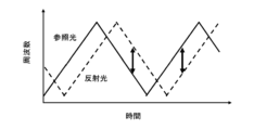
- FIG. 2 is a diagram schematically showing temporal changes in the frequencies of the reference light 20L1 and the reflected light 20L3 when the object 10 is stationary.
- a solid line represents the reference light 20L1 and a dashed line represents the reflected light 20L3.
- the frequency of the reference light 20L1 shown in FIG. 2 repeats triangular wave-like temporal changes. That is, the frequency of the reference light 20L1 repeats up-chirp and down-chirp. The increase in frequency during the up-chirp period and the decrease in frequency during the down-chirp period are equal to each other.
- the frequency of reflected light 20L3 is shifted in the positive direction along the time axis compared to the frequency of reference light 20L1.
- the amount of time shift of the reflected light 20L3 is equal to the time required for the irradiation light 20L2 to be emitted from the measuring device 100A to the outside, reflected by the object 10, and returned as the reflected light 20L3.
- the interference light 20L4 obtained by superimposing and interfering with the reference light 20L1 and the reflected light 20L3 has a frequency corresponding to the frequency difference between the frequency of the reflected light 20L3 and the frequency of the reference light 20L1.
- the double arrow shown in FIG. 2 represents the frequency difference between the two.
- the photodetector 50 outputs a signal indicating the intensity of the interference light 20L4.
- the signal is called a beat signal.
- the frequency of the beat signal, ie the beat frequency is equal to the above frequency difference.
- Processing circuitry 60 can generate measurement data about the distance of object 10 from the beat frequencies.
- the beat frequency during the up-chirp period and the beat frequency during the down-chirp period are equal to each other.
- ⁇ f is the increase or decrease in the frequency of light during the up-chirp period or the down-chirp period
- ⁇ t is the time required to change ⁇ f
- c is the speed of light
- the optical path length of the reference light 20L1 the optical path length of the irradiation light 20L2
- the optical path of the reflected light 20L3 Assuming that the difference from the total length is 2d, the beat frequency f beat in the up-chirp period or the down-chirp period is expressed by the following equation (6).
- the beat frequency f beat in Equation (6) is the time required for the irradiation light 20L2 to be emitted from the measurement device 100A to the outside, reflected by the object 10, and returned as the reflected light 20L3, at the time rate of change ⁇ f/ ⁇ t of the frequency. It is obtained by multiplying (2d/c).
- the frequency of the reflected light 20L3 is Doppler-shifted in the positive or negative direction along the frequency axis compared to the frequency of the reference light 20L1.
- the beat frequency during the up-chirp period and the beat frequency during the down-chirp period are different from each other. From the frequency difference and average of these beat frequencies, processing circuitry 60 can generate measured data regarding the velocity and distance of object 10, respectively.
- FIG. 3 is a flow chart schematically showing an example of the measurement operation performed by the processing circuit 60. As shown in FIG. The processing circuit 60 executes the operations of steps S101 to S103 shown in FIG.
- the processing circuit 60 causes the light source 20 to emit laser light 20L0 whose frequency changes with time.
- the processing circuit 60 causes the photodetector 50 to detect the interference light 20L4.
- the photodetector 50 outputs a signal corresponding to the intensity of the interference light 20L4.
- Processing circuitry 60 generates measurement data regarding the distance and/or velocity of object 10 based on the signal output from photodetector 50 .
- the above-described operation of the processing circuit 60 enables ranging and/or velocity measurement of the object 10.
- a light flow ⁇ is a flow of the reference light 20L1 from the second terminal 32a2 of the first optical splitter 32a to the photodetector 50.
- the light flow ⁇ is the flow from the third terminal 32 a 3 of the first optical splitter 32 a to the object 10 and the reflected light 20 L 3 from the object 10 to the photodetector 50 .
- the light flow ⁇ is a flow of part of the irradiation light 20L2 from the third terminal 32a3 of the first optical splitter 32a to the photodetector 50 after being reflected by the optical element 40. FIG. Such reflections occur at the interface between optical element 40 and air.
- the light flow ⁇ is the flow of another part of the irradiation light 20L2 from the third terminal 32a3 of the first optical splitter 32a to the photodetector 50 via the noise light path inside the optical circulator 34. .
- the noise light path is considered to be a path passing through the optical circulator 34, more specifically, a path along which leakage light of the irradiation light 20L2 toward the optical element 40 in the optical circulator 34 is multiple-scattered inside.
- the optical path length of the noise light path caused by internal multiple scattering is, for example, 10 times the shortest distance from the point where the irradiated light 20L2 is input to the point where the reflected light 20L3 is output in the optical circulator 34. 100 times longer.
- part of the irradiation light 20L2 is reflected by the optical element 40, and the other part is multiple-scattered inside the optical circulator 34. This is the remaining portion of the illumination light 20L2.
- the optical element 40 emits the irradiation light 20L2 to the outside.
- the range of the object 10 was measured by the following measuring device. Although the measurement apparatus has the components shown in FIG. 1, it does not satisfy the below-described conditions for reducing the influence of multiple scattered light.
- the distance from optical element 40 to object 10 was 1 m. As used herein, the distance from the optical element 40 to the object 10 refers to the distance from where the optical element 40 reflects said part of the illumination light 20L2 to where the object 10 reflects said remaining part of the illumination light 20L2. means the distance to a point.
- FIG. 4 is a graph showing the spectrum of the detection signal in the comparative example.
- the vertical and horizontal axes shown in FIG. 4 represent signal strength and frequency, respectively.
- the left end represents zero frequency and one division represents 250 MHz/512. Frequency corresponds to distance.
- the spectrum of the detection signal during the up-chirp period and the spectrum of the detection signal during the down-chirp period are superimposed. When the object 10 is stationary, the behavior of both is approximately the same.
- the peak ⁇ has a beat frequency between the reference beams 20L1, ie zero frequency.
- the peak ⁇ has a beat frequency obtained by interference between the reflected light 20L3 reflected by the object 10 and reaching the photodetector 50 and the reference light 20L1.
- the peak ⁇ has a beat frequency obtained by interference between the reference light 20L1 and the light reflected by the optical element 40 reaching the photodetector 50 in the irradiation light 20L2.
- Peak .delta. has a beat frequency that is
- the peak ⁇ is caused by the reflected light 20L3 reflected by the object 10.
- the peak ⁇ is noise and is caused by the light reflected by the optical element 40 in the irradiation light 20L2. Since the object 10 is located in front of the optical element 40, if the point where the optical element 40 reflects the illumination light 20L2 is taken as zero distance, the peak ⁇ serves as an indicator of the zero distance, albeit noise.
- the beat frequency of peak ⁇ is lower than the beat frequency of peak ⁇ , so peak ⁇ does not affect peak ⁇ . In the example shown in FIG. 4, the difference between the beat frequency of peak ⁇ and the beat frequency of peak ⁇ corresponds to a distance of 1 m.
- the peak ⁇ is noise and is caused by multiple scattered light generated inside the optical circulator 34 .
- the beat frequency of peak ⁇ is higher than the beat frequency of peak ⁇ , and the difference between them corresponds to a distance of 3.5 m.
- the peak ⁇ and the peak ⁇ are close to each other, making it difficult to determine which peak is the peak ⁇ .
- the distance to the object 10 cannot be accurately measured, resulting in a narrower distance measurement range.
- FIG. 5 is a diagram for explaining optical path lengths between components included in the measurement apparatus 100A according to the first embodiment.
- the optical path length of the first path from the second terminal 32a2 of the first optical splitter 32a to the photodetector 50 be a first optical path length d1.
- the optical path length of the second path from the third terminal 32a3 of the first optical splitter 32a to the optical element 40 is defined as a second optical path length d2.
- the optical path length of the third path from the optical element 40 to the photodetector 50 be a third optical path length d3.
- the optical path length of the fourth path from the third terminal 32a3 of the first optical splitter 32a to the photodetector 50 via the noise optical path inside the interference optical system 30, more specifically, inside the optical circulator 34, is A fourth optical path length is d4. Let the round-trip distance between the optical element 40 and the object 10 be 2L.
- the optical path length of the light flow ⁇ is the fourth optical path length d4.
- Equation (7) means that the optical path length D of the light flow ⁇ is longer than the first optical path length d1 of the light flow ⁇ .
- Equation (8) implies that the beat frequency of peak ⁇ is higher than the beat frequency of peak ⁇ .
- the fourth optical path length d4 of the light flow ⁇ may be longer or shorter than the first optical path length d1 of the light flow ⁇ . Since the optical path length of the light flow ⁇ is longer than the optical path length D of the light flow ⁇ by 2L, the beat frequency of the peak ⁇ is higher than the beat frequency of the peak ⁇ . Therefore, peak ⁇ does not affect peak ⁇ .
- Equation (9) may be used where f1 is the beat frequency of peak ⁇ and f2 is the beat frequency of peak ⁇ .
- FIG. 6 is a graph showing spectra of detection signals in the example.
- the vertical axis and horizontal axis shown in FIG. 6 are the same as the vertical axis and horizontal axis shown in FIG. 4, respectively.
- the beat frequency of peak ⁇ is higher than the beat frequency of peak ⁇
- the beat frequency of peak ⁇ is higher than the beat frequency of peak ⁇ . Therefore, in the example, the peak ⁇ and the peak ⁇ do not come close to each other, and the distance measurement range of the object 10 can be wider than in the comparative example.
- a method for calibrating the measuring device 100A according to the first embodiment is as follows. In a configuration in which the distance from the optical element 40 to the object 10 is, for example, 1 m, and the reflectance of the object 10 with respect to the irradiation light 20L2 is, for example, 10% or more, the distance of the object 10 is measured.
- Calibration object 10 can be, for example, a silver diffuser.
- the optical path lengths D and d1 are adjusted so that the relationships of equations (7) to (9) are satisfied in this configuration.
- the optical path length D can be adjusted, for example, by increasing or decreasing the length of the optical fiber connecting the optical circulator 34 and the optical element 40 to each other.
- the first optical path length d1 can be adjusted, for example, by increasing or decreasing the length of the optical fiber connecting the first optical splitter 32a and the second optical splitter 32b. If the optical fiber is wound, a large space is not required even if the optical path length D and/or d1 is lengthened.
- the optical path length from the third terminal 32a3 of the first optical splitter 32a to the photodetector 50 via the longest noise optical path inside the interference optical system 30 is selected as the fourth optical path length d4.
- the highest beat frequency among beat frequencies of a plurality of peaks ⁇ may be selected as the beat frequency f2.
- the beat frequency in the up-chirp period and the down-chirp period shown in FIG. A shift of the Doppler frequency fd results in f0 ⁇ fd.
- the distance L from the optical element 40 to the object 10 is adjusted so that f0 ⁇ fd ⁇ f1.
- FIG. 7 is a block diagram schematically showing the configuration of a modification of the measurement device according to Embodiment 1.
- FIG. A measuring apparatus 110A shown in FIG. 7 differs from the measuring apparatus 100A shown in FIG. 1 in that the interference optical system 30 includes a third optical splitter 32c instead of the optical circulator 34 shown in FIG.
- the third optical splitter 32c like the optical circulator 34, is connected to the third terminal 32a3 of the first optical splitter 32a, the second optical splitter 32b, and the optical element .
- the noise optical path is the path through the optical circulator 34.
- the first optical splitter 32a is also called “optical splitter”
- the third optical splitter 32c is also called “another optical splitter”.
- the third optical splitter 32 c inputs the irradiation light 20 L 2 to the optical element 40 .
- the optical circulator 34 inputs the reflected light 20L3 to the second optical splitter 32b.
- part of the reflected light 20L3 may return to the light source 20 via the first light splitter 32a.
- Such return light may be removed by providing an optical isolator between the light source 20 and the first optical splitter 32a.
- the distance measurement range can be widened in the same manner as in the measuring device 100A.
- FIG. 8 is a block diagram schematically showing the configuration of a measuring device according to exemplary Embodiment 2 of the present disclosure.
- the object 10 shown in FIG. 1 has been omitted.
- the measurement apparatus 100B shown in FIG. 8 is different from the measurement apparatus 100A shown in FIG. 1 in that the measurement apparatus 100B includes the fourth optical splitter 32d and the first optical element instead of the single optical element 40 shown in FIG. 40a, a second optical element 40b, and a third optical element 40c.
- the first optical element 40a, the second optical element 40b, and the third optical element 40c are also collectively referred to as "optical elements 40a to 40c.”
- the fourth optical splitter 32 d is connected to the optical circulator 34 .
- the optical elements 40a-40c are connected to a fourth optical splitter 32d. It can also be said that the optical elements 40a-40c are connected to the optical circulator 34 via the fourth optical splitter 32d.
- the fourth light splitter 32d splits the irradiation light 20L2 into first to third lights.
- the optical elements 40a to 40c emit the first to third lights to the outside, respectively, and receive the first to third reflected lights generated when the first to third lights are reflected by the object 10, respectively.
- Each of the first to third lights is part of the illumination light 20L2.
- the outputs of the first to third lights may be equal to each other or may be different from each other.
- the number of branches of the fourth optical splitter 32d is not limited, and is two or more. The same applies to the number of optical elements 40a-40c.
- the optical path lengths of the three paths from the fourth optical splitter 32d to the optical elements 40a to 40c may be equal or different.
- the zero distances of the first to third lights emitted to the outside from the optical elements 40a to 40c can be different from each other. Therefore, in the spectrum of the detection signal, first to third frequency bands corresponding to the first to third lights emitted to the outside can be assigned, respectively. As a result, from the frequency band in which the peak appears, it is possible to know which of the first to third lights used to measure the distance to the object 10 .
- the measuring apparatus 100B according to the second embodiment also has a distance measurement range as in the measuring apparatus 100A according to the first embodiment. can be expanded.
- the aforementioned second and third paths pass through the fourth optical splitter 32d.
- the optical elements 40a to 40c if the optical element having the shortest total D of the second optical path length d2 and the third optical path length d3 described above satisfies the relationships of formulas (7) to (9), the remaining optical elements also necessarily satisfy the relationships of formulas (7) to (9).
- the optical element with the shortest total D of the second optical path length d2 and the third optical path length d3 is the first optical element 40a.
- FIG. 9 is a block diagram schematically showing the configuration of a measuring device according to exemplary embodiment 3 of the present disclosure.
- the object 10 shown in FIG. 1 has been omitted.
- a measuring apparatus 100C shown in FIG. 9 differs from the measuring apparatus 100A shown in FIG. 1 in that the measuring apparatus 100C includes a fifth optical splitter 32e and a second photodetector 50b.
- the fifth optical splitter 32e is positioned between the optical circulator 34 and the optical element 40 and is connected to both.
- the second photodetector 50b is connected to the fifth optical splitter 32e.
- the optical element 40 is connected to the optical circulator 34 via the fifth optical splitter 32e.
- the first photodetector 50a is the same as the photodetector 50 shown in FIG. In this specification, the first photodetector 50a is also called “photodetector”, and the second photodetector 50b is also called “another photodetector”.
- the fifth optical splitter 32e inputs part of the irradiation light 20L2 from the third terminal 32a3 of the first optical splitter 32a to the optical element 40 as the monitor light 20L5 into the second photodetector 50b.
- the second photodetector 50b detects the monitor light 20L5.
- the output of the monitor light 20L5 can be, for example, 5% or less of the output of the irradiation light 20L2 emitted from the optical element 40 to the outside.
- the detection signal of the second photodetector 50b can be used for various purposes.
- the detection signal of the second photodetector 50b may be used as a monitor signal for controlling the operation of the light source 20 so that the emitted light 20L2 does not exceed the eye-safe reference value.
- the eye-safe reference value can be, for example, 10 mW.
- the frequency of the laser light 20L0 emitted from the light source 20 is periodically modulated. If a laser diode capable of emitting high-power laser light is used as the light source 20, such frequency modulation can be stably performed. However, since the light source 20 can emit high-power laser light, there is a possibility that the output of the laser light 20L0 may exceed the eye-safe reference value due to, for example, a failure or malfunction.
- the processing circuit 60 controls the operation of the light source 20 based on the detection signal from the second photodetector 50b so that the output of the laser light 20L0 does not exceed the eye-safe reference value.
- FIG. 10 is a flow chart schematically showing an example of the measurement operation performed by the processing circuit 60. As shown in FIG. The processing circuit 60 executes the operations of steps S201 to S206 shown in FIG.
- Steps S201, S204, and S205 The operations of steps S201, S204, and S205 are respectively the same as the operations of steps S101 to S103 shown in FIG.
- Step S202> The processing circuit 60 causes the second photodetector 50b to detect the monitor light 20L5.
- Step S203 Based on the output of the monitor light 20L5, the processing circuit 60 determines whether the output of the irradiation light 20L2 emitted from the optical element 40 to the outside is equal to or less than the eye-safe reference value. In calibrating the measurement apparatus 100C, by associating the output of the monitor light 20L5 with the output of the irradiation light 20L2 emitted to the outside, the output of the irradiation light 20L2 to be emitted to the outside can be known from the output of the monitor light 20L5. If the determination is Yes, processing circuitry 60 performs the operations of steps S204 and S205. If the determination is No, processing circuitry 60 performs the operation of step S206.
- the processing circuit 60 causes the light source 20 to stop emitting the laser light 20L0.
- the object 10 can be measured for distance and/or velocity by the irradiation light 20L2 whose output is equal to or less than the eye-safe reference value.
- FIG. 9 Flow of light in measuring device 100C
- the light flow ⁇ shown in FIG. 9 exists in the measuring device 100C shown in FIG.
- the light flows ⁇ and ⁇ pass through the fifth optical splitter 32e shown in FIG.
- the light flow ⁇ is the flow of the irradiation light 20L2 from the third terminal 32a3 of the first light splitter 32a to the first light detector 50a after being reflected by the second light detector 50b.
- the light flow ⁇ causes noise in the detected signal.
- the light flow ⁇ may narrow the distance measurement range even if the relationships of Expressions (7) to (9) are satisfied. explain.
- the range of the object 10 was measured by the following measuring device.
- the measurement apparatus has the components shown in FIG. 9, it does not satisfy the below-described conditions for reducing the influence of light reflected by the second photodetector 50b.
- FIG. 11 is a graph showing the spectrum of the detected signal in the comparative example.
- the vertical axis and horizontal axis shown in FIG. 11 are the same as the vertical axis and horizontal axis shown in FIG. 4, respectively.
- multiple peaks appear in the spectrum of the detection signal.
- the arrows shown in FIG. 11 represent representative five peaks among them.
- the peaks ⁇ to ⁇ are as described with reference to FIG.
- the peak ⁇ has a beat frequency obtained by interference between the light from the second photodetector 50b to the first photodetector 50a in the irradiation light 20L2 and the reference light 20L1.
- the peak ⁇ is noise and is caused by the light reflected by the second photodetector 50b in the illumination light 20L2.
- the beat frequency of peak ⁇ is higher than the beat frequency of peak ⁇ , and the beat frequency of peak ⁇ is higher than the beat frequency of peak ⁇ because the relationships of equations (7) through (9) are satisfied.
- Peak ⁇ is an index of zero distance.
- the beat frequency of peak ⁇ is higher than the beat frequency of peak ⁇ . Therefore, when the peak ⁇ and the peak ⁇ are close to each other, there arises a problem that the distance of the object 10 cannot be accurately measured in the frequency band near the peak ⁇ .
- FIG. 12 is a diagram for explaining optical path lengths between components included in the measuring device 100C according to the third embodiment. Let the optical path length of the fifth path from the third terminal 32a3 of the first optical splitter 32a to the second photodetector 50b be a fifth optical path length d5. Let the optical path length of the sixth path from the second photodetector 50b to the first photodetector 50a be a sixth optical path length d6.
- the condition that the above optical path length satisfies in the measurement apparatus 100C according to the third embodiment is represented by the following equation (10).
- Equation (8) implies that the beat frequency of peak ⁇ is higher than the beat frequency of peak ⁇ .
- Equation (11) may be used with the beat frequency of peak ⁇ set to f3.
- the relationships of the equations (10) and (11) are satisfied.
- the influence of the light reflected by the second photodetector 50b can be reduced, and the distance measurement range can be widened.
- Optical fibers are used for connection between components in the measuring devices 100A, 110A, 100B, and 100C described above.
- optical waveguides may be used for connection between components.
- Optical waveguides may be formed by patterning semiconductor or dielectric materials using microfabrication techniques. Also, each component and the optical waveguide may be integrated on the same substrate.
- the components of the measuring devices 100A, 110A, 100B, and 100C described above may be combined arbitrarily as long as there is no contradiction.
- the measuring device can be used, for example, for a ranging system mounted on a vehicle such as an automobile, UAV (Unmanned Aerial Vehicle), or AGV (Automated Guided Vehicle), or for vehicle detection.
- a vehicle such as an automobile, UAV (Unmanned Aerial Vehicle), or AGV (Automated Guided Vehicle), or for vehicle detection.
- UAV Unmanned Aerial Vehicle
- AGV Automatic Guided Vehicle
Abstract
計測装置は、光源と、前記光源からの光を参照光と照射光とに分離し、前記照射光が物体で反射されて生じる反射光と、前記参照光とを干渉させて干渉光を生成する干渉光学系と、前記照射光を出射し、かつ前記反射光を受ける光学素子と、前記干渉光を検出する光検出器と、を備え、前記干渉光学系は、前記光源からの前記光が入力され、かつ前記参照光および前記照射光を出力する光スプリッタを備え、前記光スプリッタから前記光検出器に至るまでの光路長をd1、前記光スプリッタから前記光学素子に至るまでの光路長をd2、前記光学素子から前記光検出器に至るまでの光路長をd3、前記光スプリッタから前記干渉光学系の内部のノイズ光経路を経て前記光検出器に至るまでの光路長をd4とするとき、d1≦d2+d3、かつ|d2+d3-d1|≧|d4-d1|の関係を満たす。
Description
本開示は、計測装置に関する。
従来、物体を光で照射し、当該物体からの反射光を検出することにより、当該物体の距離および/または速度に関する計測データを生成するLiDAR(Light Detection and Ranging)技術が存在する。LiDAR技術を用いた計測装置の典型例は、光源、光検出器、および処理回路を備える。光源は、物体を照射するための光を出射する。光検出器は、物体からの反射波を検出することにより、反射波の時間遅れに応じた信号を出力する。処理回路は、光検出器から出力された信号に基づいて、例えばFMCW(Frequency Modulated Continuous Wave)技術によって物体の距離および速度に関する計測データを生成する。特許文献1および2、ならびに非特許文献1は、FMCW技術を用いる計測装置の例を開示している。
Christopher V. P. et. al., OFC2016, W4E.3
本開示は、広い距範囲を有する計測装置を提供する。
本開示の一態様に係る計測装置は、光源と、前記光源からの光を参照光と物体を照射するための照射光とに分離し、前記照射光の少なくとも一部が前記物体で反射されて生じる反射光と、前記参照光とを干渉させて干渉光を生成する干渉光学系と、前記照射光の前記少なくとも一部を出射し、かつ前記反射光を受ける少なくとも1つの光学素子と、前記干渉光を検出する光検出器と、を備え、前記干渉光学系は、前記光源からの前記光が入力される第1端子、前記参照光を出力する第2端子、および前記照射光を出力する第3端子を有する光スプリッタを備え、前記光スプリッタの前記第2端子から前記光検出器に至るまでの第1経路の光路長をd1、前記光スプリッタの前記第3端子から前記光学素子に至るまでの第2経路の光路長をd2、前記光学素子から前記光検出器に至るまでの第3経路の光路長をd3、前記光スプリッタの前記第3端子から前記干渉光学系の内部のノイズ光経路を経て前記光検出器に至るまでの第4経路の光路長をd4とするとき、


の関係を満たす。
本開示の包括的または具体的な態様は、システム、装置、方法、集積回路、コンピュータプログラムまたはコンピュータ読み取り可能な記録ディスク等の記録媒体で実現されてもよく、システム、装置、方法、集積回路、コンピュータプログラムおよび記録媒体の任意の組み合わせで実現されてもよい。コンピュータ読み取り可能な記録媒体は、例えばCD-ROM(Compact Disc‐Read Only Memory)等の不揮発性の記録媒体を含み得る。装置は、1つ以上の装置で構成されてもよい。装置が2つ以上の装置で構成される場合、当該2つ以上の装置は、1つの機器内に配置されてもよく、分離した2つ以上の機器内に分かれて配置されてもよい。本明細書および特許請求の範囲では、「装置」とは、1つの装置を意味し得るだけでなく、複数の装置からなるシステムも意味し得る。
本開示の技術によれば、広い距範囲を有する計測装置を実現できる。
本開示において、回路、ユニット、装置、部材または部の全部または一部、またはブロック図における機能ブロックの全部または一部は、例えば、半導体装置、半導体集積回路(IC)、またはLSI(large scale integration)を含む1つまたは複数の電子回路によって実行され得る。LSIまたはICは、1つのチップに集積されてもよいし、複数のチップを組み合わせて構成されてもよい。例えば、記憶素子以外の機能ブロックは、1つのチップに集積されてもよい。ここでは、LSIまたはICと呼んでいるが、集積の度合いによって呼び方が変わり、システムLSI、VLSI(very large scale integration)、もしくはULSI(ultra large scale integration)と呼ばれるものであってもよい。LSIの製造後にプログラムされる、Field Programmable Gate Array(FPGA)、またはLSI内部の接合関係の再構成またはLSI内部の回路区画のセットアップができるreconfigurable logic deviceも同じ目的で使うことができる。
さらに、回路、ユニット、装置、部材または部の全部または一部の機能または操作は、ソフトウェア処理によって実行することが可能である。この場合、ソフトウェアは1つまたは複数のROM、光学ディスク、ハードディスクドライブなどの非一時的記録媒体に記録され、ソフトウェアが処理装置(processor)によって実行されたときに、そのソフトウェアで特定された機能が処理装置(processor)および周辺装置によって実行される。システムまたは装置は、ソフトウェアが記録されている1つまたは複数の非一時的記録媒体、処理装置(processor)、および必要とされるハードウェアデバイス、例えばインターフェースを備えていてもよい。
本開示において、「光」とは、可視光(波長が約400nm~約700nm)だけでなく、紫外線(波長が約10nm~約400nm)および赤外線(波長が約700nm~約1mm)を含む電磁波を意味する。本明細書において、紫外線を「紫外光」と称し、赤外線を「赤外光」とも称する。
以下、本開示の例示的な実施形態を説明する。なお、以下で説明する実施形態は、いずれも包括的又は具体的な例を示すものである。以下の実施形態で示される数値、形状、構成要素、構成要素の配置位置及び接続形態、ステップ、ステップの順序などは、一例であり、本開示を限定する主旨ではない。また、以下の実施形態における構成要素のうち、最上位概念を示す独立請求項に記載されていない構成要素については、任意の構成要素として説明される。また、各図は模式図であり、必ずしも厳密に図示されたものではない。さらに、各図において、実質的に同一の構成要素に対しては同一の符号を付しており、重複する説明は省略又は簡略化される場合がある。
まず、本開示の基礎となった知見を説明する。近年、距離に関して広いダイナミックレンジと高い分解能を両立し、外乱の影響を受けにくく、高速に移動する物体の速度を検出できるFMCW-LiDAR技術が開発されている。ミリ波ではなく光を利用することにより、物体を照射する光のスポット径を相対的に小さくすることができ、物体の計測データをより正確に取得することが可能になる。
FMCW-LiDAR技術を用いる計測装置では、内部散乱光が生じることがある。特許文献1は、光を外部に出射する光アンテナで生じる内部散乱光を計測開始のトリガとすることによって正確に測距を行う方法を開示している。特許文献1に開示されている内部散乱光は、測距精度の向上に役立てることができる。一方で、本発明者は、FMCW-LiDAR技術を用いる計測装置には、特許文献1に開示されている内部散乱光とは別に、光学部品の内部で生じると考えられる多重散乱光が存在し、そのような多重散乱光は測距範囲を狭めてしまう可能性があることを見出した。
FMCW-LiDAR技術を用いる本開示のある実施形態による計測装置では、内部の構成要素間の光路長を適切に設計することにより、多重散乱光の影響を低減することができ、測距範囲を広げることが可能になる。以下に、本開示の実施形態による計測装置を説明する。
第1の項目に係る計測装置は、光源と、前記光源からの光を参照光と物体を照射するための照射光とに分離し、前記照射光の少なくとも一部が前記物体で反射されて生じる反射光と、前記参照光とを干渉させて干渉光を生成する干渉光学系と、前記照射光の前記少なくとも一部を出射し、かつ前記反射光を受ける少なくとも1つの光学素子と、前記干渉光を検出する光検出器と、を備える。前記干渉光学系は、前記光源からの前記光が入力される第1端子、前記参照光を出力する第2端子、および前記照射光を出力する第3端子を有する光スプリッタを備える。前記光スプリッタの前記第2端子から前記光検出器に至るまでの第1経路の光路長をd1、前記光スプリッタの前記第3端子から前記光学素子に至るまでの第2経路の光路長をd2、前記光学素子から前記光検出器に至るまでの第3経路の光路長をd3、前記光スプリッタの前記第3端子から前記干渉光学系の内部のノイズ光経路を経て前記光検出器に至るまでの第4経路の光路長をd4とするとき、前記計測装置は、


の関係を満たす。
この計測装置では、干渉光学系の内部で生じる多重散乱光の影響を低減して測距範囲を広げることができる。
第2の項目に係る計測装置は、第1の項目に係る計測装置において、前記干渉光学系が、光サーキュレータを備える。前記光サーキュレータは、前記光スプリッタの前記第3端子および前記少なくとも1つの光学素子に接続されている。前記光検出器は、前記光スプリッタの前記第2端子および前記光サーキュレータに接続されている。前記ノイズ光経路は、前記光サーキュレータを通る経路である。
この計測装置では、光サーキュレータの内部で生じる多重散乱光の影響を低減して測距範囲を広げることができる。
第3の項目に係る計測装置は、第1の項目に係る計測装置において、前記干渉光学系が、前記干渉光学系は、他の光スプリッタを備える。前記他の光スプリッタは、前記光スプリッタの前記第3端子および前記少なくとも1つの光学素子に接続されている。前記光検出器は、前記光スプリッタの前記第2端子および前記他の光スプリッタに接続されている。前記ノイズ光経路は、前記他の光スプリッタを通る経路である。
この計測装置では、他の光スプリッタの内部で生じる多重散乱光の影響を低減して測距範囲を広げることができる。
第4の項目に係る計測装置は、第1から第3の項目のいずれかに係る計測装置において、前記少なくとも1つの光学素子が複数の光学素子を含み、前記複数の光学素子の各々は前記照射光の一部を出射する。前記計測装置は、前記複数の光学素子の各々について、式(1)および式(2)の関係を満たす。
この計測装置では、光学素子の数が複数であっても、測距範囲を広げることができる。
第5の項目に係る計測装置は、光源と、前記光源からの光を参照光と物体を照射するための照射光とに分離し、前記照射光の少なくとも一部が前記物体で反射されて生じる反射光と、前記参照光とを干渉させて干渉光を生成する干渉光学系と、前記照射光の前記少なくとも一部を出射し、かつ前記反射光を受ける少なくとも1つの光学素子と、前記干渉光を検出する光検出器と、他の光検出器とを備える。前記干渉光学系は、前記光源からの前記光が入力される第1端子、前記参照光を出力する第2端子、および前記照射光を出力する第3端子を有する光スプリッタを備える。前記他の光検出器は、前記光スプリッタの前記第3端子から前記光学素子までの前記照射光の一部を検出する。前記光スプリッタの前記第2端子から前記光検出器に至るまでの第1経路の光路長をd1、前記光スプリッタの前記第3端子から前記光学素子に至るまでの第2経路の光路長をd2、前記光学素子から前記光検出器に至るまでの第3経路の光路長をd3、前記光スプリッタの前記第3端子から前記他の光検出器に至るまでの第5経路の光路長をd5、前記他の光検出器から前記光検出器に至るまでの第6経路の光路長をd6とするとき、前記計測装置は、


の関係を満たす。
この計測装置では、他の光検出器で反射される光の影響を低減して測距範囲を広げることができる。
第6の項目に係る計測装置は、第1から第5の項目に係る計測装置において、前記光検出器から出力される信号を処理する処理回路を備える。前記光源は、前記光の周波数を変化させることが可能である。
この計測装置では、FMCW-LiDAR技術によって測距および/または測速することができる。
第7の項目に係る計測装置は、光源と、前記光源からの光を参照光と物体を照射するための照射光とに分離し、前記照射光の少なくとも一部が前記物体で反射されて生じる反射光と、前記参照光とを干渉させて干渉光を生成する干渉光学系と、前記照射光の前記少なくとも一部を出射し、かつ前記反射光を受ける少なくとも1つの光学素子と、前記干渉光を検出する光検出器と、を備える。前記計測装置は、前記照射光のうち、前記光学素子で反射されて前記光検出器に至る光と、前記参照光との干渉によるビート周波数をf1、前記照射光のうち、前記干渉光学系の内部のノイズ光経路を経て前記光検出器に至る光と、前記参照光との干渉によるビート周波数をf2とするとき、

の関係を満たす。
この計測装置では、干渉光学系の内部で生じる多重散乱光の影響を低減して測距範囲を広げることができる。
第8の項目に係る計測装置は、第7の項目に係る計測装置において、前記干渉光学系が、前記照射光の前記少なくとも一部を前記少なくとも1つの光学素子に入力し、かつ前記反射光を前記光検出器に入力する光サーキュレータを備える。前記ノイズ光経路は、前記光サーキュレータを通る経路である。
この計測装置では、光サーキュレータの内部で生じる多重散乱光の影響を低減して測距範囲を広げることができる。
第9の項目に係る計測装置は、第7の項目に係る計測装置において、前記干渉光学系が、他の光スプリッタを備える。前記他の光スプリッタは、前記照射光の前記少なくとも一部を前記少なくとも1つの光学素子に入力し、かつ前記反射光を前記光検出器に入力する。前記ノイズ光経路は、前記他の光スプリッタを通る経路である。
この計測装置では、他の光スプリッタの内部で生じる多重散乱光の影響を低減して測距範囲を広げることができる。
第10の項目に係る計測装置は、前記少なくとも1つの光学素子が複数の光学素子を含み、前記複数の光学素子の各々は前記照射光の一部を出射する。前記計測装置は、前記複数の光学素子の各々について、式(4)の関係を満たす。
この計測装置では、光学素子の数が複数であっても、測距範囲を広げることができる。
第11の項目に係る計測装置は、光源と、前記光源からの光を参照光と物体を照射するための照射光とに分離し、前記照射光の少なくとも一部が前記物体で反射されて生じる反射光と、前記参照光とを干渉させて干渉光を生成する干渉光学系と、前記照射光の前記少なくとも一部を出射し、かつ前記反射光を受ける少なくとも1つの光学素子と、前記干渉光を検出する光検出器と、前記干渉光学系から前記光学素子までの前記照射光の一部を検出する他の光検出器と、を備える。前記照射光のうち、前記光学素子で反射されて前記光検出器に至る光と、前記参照光との干渉によるビート周波数をf1、前記照射光のうち、前記他の光検出器から前記光検出器に至る光と、前記参照光との干渉によるビート周波数をf3とするとき、前記計測装置は、

の関係を満たす。
この計測装置では、他の光検出器で反射される光の影響を低減して測距範囲を広げることができる。
第12の項目に係る計測装置は、第7から第11の項目のいずれかに係る計測装置において、前記光検出器から出力される信号を処理する処理回路を備える。前記光源は、前記光の周波数を変化させることが可能である。
この計測装置では、FMCW-LiDAR技術によって測距および/または測速することができる。
(実施形態1)
[計測装置]
まず、図1を参照して、本開示の実施形態1による計測装置の構成例を説明する。図1は、本開示の例示的な実施形態1による計測装置の構成を模式的に示すブロック図である。図1には、計測対象の物体10が示されている。図1に示す計測装置100Aは、光源20と、干渉光学系30と、光学素子40と、光検出器50と、処理回路60と、メモリ62とを備える。干渉光学系30は、第1光スプリッタ32aと、第2光スプリッタ32bと、光サーキュレータ34とを備える。図1に示す太線は、2つの構成要素を互いに接続する光ファイバを表す。図1に示す矢印付きの実線は信号の送受信を表す。図1に示す矢印付きの破線は光の流れを表す。
後述するように、光サーキュレータ34では多重散乱光が生じると考えられ、そのことが原因で測距範囲が狭くなる可能性がある。実施形態1による計測装置100Aでは、内部の構成要素間の光路長を適切に設計することにより、そのような多重散乱光の影響を低減することができ、測距範囲を広げることが可能になる。多重散乱光の影響を低減する具体的な条件については詳細を後述する。
以下に、計測装置100Aの構成要素を説明する。
光源20は、レーザ光20L0を出射する。光源20は、レーザ光20L0の周波数を変化させることが可能である。周波数は、例えば三角波状またはのこぎり状に一定の時間周期で時間変化され得る。当該時間周期は、例えば1μ秒以上10m秒以下であり得る。当該時間周期は変動してもよい。周波数の変化幅は、例えば100MHz以上1THz以下であり得る。レーザ光20L0の波長は、例えば700nm以上2000nm以下の近赤外光の波長域に含まれ得る。太陽光は近赤外光および可視光を有し、近赤外光の光量は可視光の光量より少ないので、レーザ光20L0として近赤外光を使用すれば、太陽光のノイズとしての影響を低減することができる。レーザ光20L0の波長は必ずしも近赤外光の波長域に含まれる必要はない。レーザ光20L0の波長は、400nm以上700nm以下の可視光の波長域に含まれていてもよいし、紫外光の波長域に含まれていてもよい。光源20は、例えば、分布帰還型レ―ザダイオード、または外部共振器型レ―ザダイオードを備え得る。これらのレーザダイオードは、安価かつ小型であり、単一モード発振が可能であり、印加する電流量に応じてレーザ光20L0の周波数を変化させることができる。
干渉光学系30に含まれる第1光スプリッタ32aは、光源20から出射されるレーザ光20L0を、参照光20L1と、物体10を照射するための照射光20L2とに分離する。第1光スプリッタ32aは、さらに、参照光20L1を第2光スプリッタ32bに入力し、照射光20L2を光サーキュレータ34に入力する。第1光スプリッタ32aは、レーザ光20L0が入力される第1端子32a1と、参照光20L1を出力する第2端子32a2と、照射光20L2を出力する第3端子32a3とを有する。
干渉光学系30に含まれる光サーキュレータ34は、照射光20L2を光学素子40に入力し、物体10を照射光20L2で照射して生じた反射光20L3を第2光スプリッタ32bに入力する。光サーキュレータ34は、第1光スプリッタ32aの第3端子32a3、第2光スプリッタ32b、および光学素子40に接続されている。
干渉光学系30に含まれる第2光スプリッタ32bは、参照光20L1および反射光20L3を重畳して干渉させた干渉光20L4を光検出器50に入力する。第2光スプリッタ32bは、第1光スプリッタ32aと同様に、参照光20L1および反射光20L3の入力、ならびに干渉光20L4の出力のための3つの端子を有する。
光学素子40は、照射光20L2を外部に出射し、かつ反射光20L3を受ける。本明細書において、光学素子40から照射光20L2が出射される方向を「前方」とも称する。光学素子40は、例えば照射光20L2をコリメートするコリメータレンズであり得る。本明細書において、「コリメート」とは、照射光20L2を平行光にする場合だけでなく、照射光20L2の広がりを低減する場合も意味する。あるいは、光学素子40は、照射光20L2を、0次回折光および/または±N次回折光(Nは自然数)として外部に出射する回折格子であってもよい。互いに異なる方向に出射される複数の回折光によって物体10を測距することにより、物体10の測距の角度範囲を広げることができる。以下の説明において、光学素子40はコリメータレンズであるとする。
計測装置100Aにおいて、照射光20L2が干渉光学系30から物体10に至るまでの経路と、反射光20L3が物体10から干渉光学系30に至るまでの経路とは互いに重なる。このような同軸光学系を採用することにより、計測装置100Aの構成を単純化でき、安定した計測を実現できる。
光検出器50は、干渉光20L4を検出する。光検出器50は、1つまたは複数の光検出素子を含む。光検出素子は、干渉光20L4の強度に対応する信号を出力する。光検出器50は、第2光スプリッタ32bを介して、第1光スプリッタ32aの第2端子32a2、および光サーキュレータ34に接続されている。
処理回路60は、光源20および光検出器50の動作を制御する。処理回路60は、FMCW-LiDAR技術を用いて、光検出器50から出力された信号を処理する。処理回路60は、当該信号に基づいて、物体10の距離および/または速度に関する計測データを生成して出力する。処理回路60の動作の詳細については後述する。
処理回路60によって実行されるコンピュータプログラムは、ROMまたはRAM(Random Access Memory)などのメモリ62に格納されている。このように、計測装置100Aは、処理回路60およびメモリ62を含む処理装置を備える。処理回路60およびメモリ62は、1つの回路基板に集積されていてもよいし、別々の回路基板に設けられていてもよい。処理回路60の制御および信号処理の機能が、複数の回路に分散していてもよい。処理装置は、他の構成要素から離れた遠隔地に設置され、有線または無線の通信ネットワークを介して、光源20および光検出器50の動作を制御してもよい。
[FMCW-LiDAR技術]
次に、図2を参照して、FMCW-LiDAR技術を簡単に説明する。FMCW-LiDAR技術の詳細は、例えば非特許文献1に開示されている。
次に、図2を参照して、FMCW-LiDAR技術を簡単に説明する。FMCW-LiDAR技術の詳細は、例えば非特許文献1に開示されている。
図2は、物体10が静止している場合の、参照光20L1および反射光20L3の周波数の時間変化を模式的に示す図である。実線は参照光20L1を表し、破線は反射光20L3を表す。図2に示す参照光20L1の周波数は、三角波状の時間変化を繰り返す。すなわち、参照光20L1の周波数は、アップチャープとダウンチャープとを繰り返す。アップチャープ期間における周波数の増加分と、ダウンチャープ期間における周波数の減少分とは互いに等しい。反射光20L3の周波数は、参照光20L1の周波数と比較して、時間軸に沿って正方向にシフトする。反射光20L3の時間がシフトする量は、照射光20L2が計測装置100Aから外部に出射され、物体10で反射されて反射光20L3として戻ってくるまでの時間に等しい。その結果、参照光20L1と反射光20L3とが重畳されて干渉した干渉光20L4は、反射光20L3の周波数と参照光20L1の周波数との周波数差に相当する周波数を有する。図2に示す両矢印は、両者の周波数差を表す。光検出器50は、干渉光20L4の強度を示す信号を出力する。当該信号はビート信号と呼ばれる。ビート信号の周波数、すなわちビート周波数は、上記の周波数差に等しい。処理回路60は、ビート周波数から、物体10の距離に関する計測データを生成することができる。
物体10が静止している場合、アップチャープ期間におけるビート周波数と、ダウンチャープ期間におけるビート周波数とは互いに等しい。アップチャープ期間またはダウンチャープ期間における光の周波数の増減分をΔf、Δfの変化に要する時間をΔt、光速をc、参照光20L1の光路長と、照射光20L2の光路長および反射光20L3の光路長の合計との差を2dとすると、アップチャープ期間またはダウンチャープ期間におけるビート周波数fbeatは、以下の式(6)によって表される。

式(6)のビート周波数fbeatは、周波数の時間変化率Δf/Δtに、照射光20L2が計測装置100Aから外部に出射され、物体10で反射されて反射光20L3として戻ってくるまでの時間(2d/c)を乗算することによって得られる。
物体10が移動する場合、反射光20L3の周波数は、参照光20L1の周波数と比較して、周波数軸に沿って正方向または負方向にドップラーシフトする。この場合、アップチャープ期間におけるビート周波数と、ダウンチャープ期間におけるビート周波数とは互いに異なる。処理回路60は、これらのビート周波数の周波数差および平均から、物体10の速度および距離に関する計測データをそれぞれ生成することができる。
[処理回路60が実行する動作]
次に、図3を参照して、実施形態1において処理回路60が実行する動作の例を説明する。図3は、処理回路60が実行する計測動作の例を概略的に示すフローチャートである。処理回路60は、図3に示すステップS101からS103の動作を実行する。
次に、図3を参照して、実施形態1において処理回路60が実行する動作の例を説明する。図3は、処理回路60が実行する計測動作の例を概略的に示すフローチャートである。処理回路60は、図3に示すステップS101からS103の動作を実行する。
<ステップS101>
処理回路60は、周波数が時間変化するレーザ光20L0を光源20に出射させる。
処理回路60は、周波数が時間変化するレーザ光20L0を光源20に出射させる。
<ステップS102>
処理回路60は、干渉光20L4を光検出器50に検出させる。光検出器50は、干渉光20L4の強度に対応する信号を出力する。
処理回路60は、干渉光20L4を光検出器50に検出させる。光検出器50は、干渉光20L4の強度に対応する信号を出力する。
<ステップS103>
処理回路60は、光検出器50から出力された信号に基づいて、物体10の距離および/または速度に関する計測データを生成する。
処理回路60は、光検出器50から出力された信号に基づいて、物体10の距離および/または速度に関する計測データを生成する。
処理回路60の上記の動作により、物体10の測距および/または測速が可能になる。
[計測装置100Aにおける光の流れ]
再び図1を参照する。図1に示す計測装置100Aには、矢印付きの破線によって表されるように、複数の光の流れが生じる。光の流れαは、参照光20L1が第1光スプリッタ32aの第2端子32a2から光検出器50に至るまでの流れである。光の流れβは、照射光20L2が第1光スプリッタ32aの第3端子32a3から物体10に至り、反射光20L3が物体10から光検出器50に至るまでの流れである。
再び図1を参照する。図1に示す計測装置100Aには、矢印付きの破線によって表されるように、複数の光の流れが生じる。光の流れαは、参照光20L1が第1光スプリッタ32aの第2端子32a2から光検出器50に至るまでの流れである。光の流れβは、照射光20L2が第1光スプリッタ32aの第3端子32a3から物体10に至り、反射光20L3が物体10から光検出器50に至るまでの流れである。
一方で、複数の光の流れの中には、光の流れαおよびβの他に、検出信号にノイズを引き起こす光の流れγおよびδが存在する。光の流れγは、照射光20L2の一部が、第1光スプリッタ32aの第3端子32a3から、光学素子40で反射されて光検出器50に至るまでの流れである。そのような反射は、光学素子40と空気との界面で生じる。光の流れδは、照射光20L2の他の一部が、第1光スプリッタ32aの第3端子32a3から、光サーキュレータ34の内部のノイズ光経路を経て光検出器50に至るまでの流れである。ノイズ光経路は、光サーキュレータ34を通る経路、より具体的には、光サーキュレータ34において光学素子40に向かう照射光20L2の漏れ光が、内部で多重散乱されながら進む経路であると考えられる。内部の多重散乱に起因するノイズ光経路の光路長は、光サーキュレータ34のうち、照射光20L2が入力される箇所から反射光20L3を出力する箇所までの最短距離と比較して、例えば10倍から100倍程度長い。
上記のように、照射光20L2の一部は光学素子40で反射され、他の一部は光サーキュレータ34の内部で多重散乱されるので、実際に光学素子40から外部に出射されるのは、照射光20L2の残りの部分である。ただし、本明細書では、誤解が生じない限り、「光学素子40は、照射光20L2を外部に出射する」のように記載する。
以下に、図4を参照して、光の流れγは測距範囲に影響を及ぼさない一方、光の流れδは測距範囲を狭めてしまう可能性があることを比較例と共に説明する。比較例では、以下の計測装置によって物体10が測距された。当該計測装置は、図1に示す構成要素を備えるが、多重散乱光の影響を低減する後述の条件を満たしていない。比較例において、光学素子40から物体10までの距離は1mであった。本明細書において、光学素子40から物体10までの距離とは、光学素子40が照射光20L2の上記の一部を反射する箇所から、物体10が照射光20L2の上記の残りの部分を反射する箇所までの距離を意味する。
図4は、比較例における検出信号のスペクトルを示すグラフである。図4に示す縦軸および横軸は、信号の強度および周波数をそれぞれ表す。横軸について、左端はゼロ周波数を表し、1つ目盛りは250MHz/512を表す。周波数は距離に対応する。図4では
、アップチャープ期間における検出信号のスペクトルとダウンチャープ期間における検出信号のスペクトルとが重ねて示されている。物体10が静止している場合、両者の振る舞いはほぼ同じである。
、アップチャープ期間における検出信号のスペクトルとダウンチャープ期間における検出信号のスペクトルとが重ねて示されている。物体10が静止している場合、両者の振る舞いはほぼ同じである。
図4に示すように、検出信号のスペクトルには複数のピークが現れる。図4に示す矢印は、そのうちの代表的な4つのピークを表す。ピークαは、参照光20L1同士のビート周波数、すなわちゼロ周波数を有する。ピークβは、物体10で反射されて光検出器50に至る反射光20L3と、参照光20L1との干渉によって得られるビート周波数を有する。ピークγは、照射光20L2のうち、光学素子40で反射されて光検出器50に至る光と、参照光20L1との干渉によって得られるビート周波数を有する。ピークδは、照射光20L2のうち、干渉光学系30の内部、より具体的には光サーキュレータ34の内部のノイズ光経路を経て光検出器50に至る光と、参照光20L1との干渉によって得られるビート周波数を有する。
ピークβは、物体10で反射される反射光20L3に起因して生じる。ピークγはノイズであり、照射光20L2のうち、光学素子40で反射される光に起因して生じる。物体10は光学素子40よりも前方に位置するので、光学素子40が照射光20L2を反射する箇所をゼロ距離とすると、ピークγは、ノイズではあるがゼロ距離の指標として役立つ。ピークγのビート周波数は、ピークβのビート周波数よりも低いので、ピークγは、ピークβに影響を及ぼさない。図4に示す例において、ピークβのビート周波数と、ピークγのビート周波数との差は、1mの距離に相当する。
ピークδはノイズであり、光サーキュレータ34の内部で生じる多重散乱光に起因して生じる。ピークδのビート周波数はピークγのビート周波数よりも高く、両者の差は3.5mの距離に相当する。光学素子40から物体10までの距離が約3.5mである場合、ピークβとピークδとが互いに近接してしまうため、どちらのピークがピークβであるかの判別が容易ではなくなる。その結果、ピークδ付近の周波数帯域では、物体10を正確に測距できず、測距範囲が狭くなるという課題が生じる。
[多重散乱光の影響を低減する条件]
以下に、図5を参照して、上記の課題を解決するために計測装置100Aが満たす条件を説明する。図5は、実施形態1による計測装置100Aに含まれる構成要素間の光路長を説明するための図である。第1光スプリッタ32aの第2端子32a2から光検出器50に至るまでの第1経路の光路長を第1光路長d1とする。第1光スプリッタ32aの第3端子32a3から光学素子40に至るまでの第2経路の光路長を第2光路長d2とする。光学素子40から光検出器50に至るまでの第3経路の光路長を第3光路長d3とする。第1光スプリッタ32aの第3端子32a3から、干渉光学系30の内部、より具体的には光サーキュレータ34の内部のノイズ光経路を経て光検出器50に至るまでの第4経路の光路長を第4光路長d4とする。光学素子40と物体10との往復距離を2Lとする。
以下に、図5を参照して、上記の課題を解決するために計測装置100Aが満たす条件を説明する。図5は、実施形態1による計測装置100Aに含まれる構成要素間の光路長を説明するための図である。第1光スプリッタ32aの第2端子32a2から光検出器50に至るまでの第1経路の光路長を第1光路長d1とする。第1光スプリッタ32aの第3端子32a3から光学素子40に至るまでの第2経路の光路長を第2光路長d2とする。光学素子40から光検出器50に至るまでの第3経路の光路長を第3光路長d3とする。第1光スプリッタ32aの第3端子32a3から、干渉光学系30の内部、より具体的には光サーキュレータ34の内部のノイズ光経路を経て光検出器50に至るまでの第4経路の光路長を第4光路長d4とする。光学素子40と物体10との往復距離を2Lとする。
検出信号にノイズを引き起こすのは、図1に示す光の流れγおよびδである。光の流れγの光路長は、第2光路長および第3光路長の合計、すなわちD=d2+d3である。光の流れδの光路長は第4光路長d4である。検出信号のスペクトルにおいて、ピークγのビート周波数がピークδのビート周波数よりも高ければ、ピークβとピークδとが互いに近接することはないので、上記の課題は生じず、物体10の測距範囲を広くすることができる。実施形態1による計測装置100Aにおいて上記の光路長が満たす条件は、以下の式(7)および式(8)によって表される。


式(7)は、光の流れγの光路長Dが光の流れαの第1光路長d1よりも長いことを意味する。式(8)は、ピークγのビート周波数がピークδのビート周波数よりも高いことを意味する。式(8)の右辺において、光の流れδの第4光路長d4は、光の流れαの第1光路長d1よりも長くてもよいし、短くてもよい。光の流れβの光路長は、光の流れγの光路長Dよりも2Lの分だけ長いので、ピークβのビート周波数は、ピークγのビート周波数よりも高くなる。したがって、ピークγは、ピークβに影響を及ぼさない。
式(8)の代わりに、ピークγのビート周波数をf1、ピークδのビート周波数をf2として、式(9)を用いてもよい。

実施形態1による計測装置100Aでは、式(7)から式(9)の関係が満たされるので、干渉光学系30の内部における多重散乱光の影響を低減することができ、測距範囲を広げることが可能になる。
次に、図6を参照して、実施形態1による計測装置100Aによって物体10を測距した実施例を説明する。図6は、実施例における検出信号のスペクトルを示すグラフである。図6に示す縦軸および横軸は、図4に示す縦軸および横軸とそれぞれ同じである。図6に示すように、ピークγのビート周波数はピークδのビート周波数よりも高く、ピークβのビート周波数は、ピークγのビート周波数よりも高い。したがって、実施例では、ピークβとピークδとが互いに近接することがなく、比較例よりも物体10の測距範囲を広げることができる。
[計測装置100Aの校正方法]
実施形態1による計測装置100Aの校正方法は以下の通りである。光学素子40から物体10までの距離が例えば1mであり、物体10の照射光20L2に対する反射率が例えば10%以上である構成において、物体10が測距される。校正用の物体10は、例えば銀拡散板であり得る。当該構成において式(7)から式(9)の関係が満たされるように、光路長Dおよびd1が調整される。光路長Dは、例えば、光サーキュレータ34と光学素子40とを互いに接続する光ファイバの長さを増減することによって調整できる。同様に、第1光路長d1は、例えば、第1光スプリッタ32aと第2光スプリッタ32bとを互いに接続する光ファイバの長さを増減することによって調整できる。光ファイバを巻回すれば、光路長Dおよび/またはd1を長くしても大きなスペースを取ることはない。
実施形態1による計測装置100Aの校正方法は以下の通りである。光学素子40から物体10までの距離が例えば1mであり、物体10の照射光20L2に対する反射率が例えば10%以上である構成において、物体10が測距される。校正用の物体10は、例えば銀拡散板であり得る。当該構成において式(7)から式(9)の関係が満たされるように、光路長Dおよびd1が調整される。光路長Dは、例えば、光サーキュレータ34と光学素子40とを互いに接続する光ファイバの長さを増減することによって調整できる。同様に、第1光路長d1は、例えば、第1光スプリッタ32aと第2光スプリッタ32bとを互いに接続する光ファイバの長さを増減することによって調整できる。光ファイバを巻回すれば、光路長Dおよび/またはd1を長くしても大きなスペースを取ることはない。
干渉光学系30の内部において複数のノイズ光経路が存在する場合、検出信号のスペクトルに複数のピークδが現れる。その場合、第1光スプリッタ32aの第3端子32a3から、干渉光学系30の内部の最も長いノイズ光経路を経て光検出器50に至るまでの経路の光路長を第4光路長d4として選択してもよい。同様に、複数のピークδのビート周波数のうち、最も高いビート周波数をビート周波数f2として選択してもよい。
前述した例とは異なり、物体10が移動する場合、図2に示すアップチャープ期間およびダウンチャープ期間におけるビート周波数は、物体10の距離に応じた周波数f0を中心に、物体10の速度に依存したドップラー周波数fdの分だけずれてf0±fdになる。その場合、f0-fd≧f1になるように、光学素子40から物体10までの距離Lが調整される。
(実施形態1の変形例)
次に、図7を参照して、本開示の実施形態1による計測装置100Aの変形例を説明する。図7は、実施形態1による計測装置の変形例の構成を模式的に示すブロック図である。図7に示す計測装置110Aが図1に示す計測装置100Aとは異なる点は、干渉光学系30が、図1に示す光サーキュレータ34の代わりに、第3光スプリッタ32cを備えることである。第3光スプリッタ32cは、光サーキュレータ34と同様に、第1光スプリッタ32aの第3端子32a3、第2光スプリッタ32b、および光学素子40に接続されている。計測装置110Aにおいて、ノイズ光経路は、光サーキュレータ34を通る経路である。本明細書において、第1光スプリッタ32aを「光スプリッタ」とも称し、第3光スプリッタ32cを「他の光スプリッタ」とも称する。第3光スプリッタ32cは、照射光20L2を光学素子40に入力する。光サーキュレータ34は、反射光20L3を第2光スプリッタ32bに入力する。ただし、第3光スプリッタ32cでは、反射光20L3の一部が、第1光スプリッタ32aを介して、光源20に戻る可能性がある。そのような戻り光は、光源20と第1光スプリッタ32aとの間に光アイソレータを設けて除去してもよい。計測装置110Aにおいても、計測装置100Aと同様に、測距範囲を広げることができる。
次に、図7を参照して、本開示の実施形態1による計測装置100Aの変形例を説明する。図7は、実施形態1による計測装置の変形例の構成を模式的に示すブロック図である。図7に示す計測装置110Aが図1に示す計測装置100Aとは異なる点は、干渉光学系30が、図1に示す光サーキュレータ34の代わりに、第3光スプリッタ32cを備えることである。第3光スプリッタ32cは、光サーキュレータ34と同様に、第1光スプリッタ32aの第3端子32a3、第2光スプリッタ32b、および光学素子40に接続されている。計測装置110Aにおいて、ノイズ光経路は、光サーキュレータ34を通る経路である。本明細書において、第1光スプリッタ32aを「光スプリッタ」とも称し、第3光スプリッタ32cを「他の光スプリッタ」とも称する。第3光スプリッタ32cは、照射光20L2を光学素子40に入力する。光サーキュレータ34は、反射光20L3を第2光スプリッタ32bに入力する。ただし、第3光スプリッタ32cでは、反射光20L3の一部が、第1光スプリッタ32aを介して、光源20に戻る可能性がある。そのような戻り光は、光源20と第1光スプリッタ32aとの間に光アイソレータを設けて除去してもよい。計測装置110Aにおいても、計測装置100Aと同様に、測距範囲を広げることができる。
(実施形態2)
次に、図8を参照して、本開示の実施形態2による計測装置の構成例を説明する。図8は、本開示の例示的な実施形態2による計測装置の構成を模式的に示すブロック図である。図1に示す物体10は省略されている。図8に示す計測装置100Bが図1に示す計測装置100Aとは異なる点は、計測装置100Bが、図1に示す単一の光学素子40ではなく、第4光スプリッタ32dと、第1光学素子40aと、第2光学素子40bと、第3光学素子40cとを備えることである。本明細書において、第1光学素子40a、第2光学素子40b、および第3光学素子40cをまとめて「光学素子40a~40c」とも称する。第4光スプリッタ32dは、光サーキュレータ34に接続されている。光学素子40a~40cは、第4光スプリッタ32dに接続されている。光学素子40a~40cは、第4光スプリッタ32dを介して光サーキュレータ34に接続されていると言うこともできる。
次に、図8を参照して、本開示の実施形態2による計測装置の構成例を説明する。図8は、本開示の例示的な実施形態2による計測装置の構成を模式的に示すブロック図である。図1に示す物体10は省略されている。図8に示す計測装置100Bが図1に示す計測装置100Aとは異なる点は、計測装置100Bが、図1に示す単一の光学素子40ではなく、第4光スプリッタ32dと、第1光学素子40aと、第2光学素子40bと、第3光学素子40cとを備えることである。本明細書において、第1光学素子40a、第2光学素子40b、および第3光学素子40cをまとめて「光学素子40a~40c」とも称する。第4光スプリッタ32dは、光サーキュレータ34に接続されている。光学素子40a~40cは、第4光スプリッタ32dに接続されている。光学素子40a~40cは、第4光スプリッタ32dを介して光サーキュレータ34に接続されていると言うこともできる。
第4光スプリッタ32dは、照射光20L2を第1から第3の光に分岐する。光学素子40a~40cは、第1から第3の光をそれぞれ外部に出射し、かつ、第1から第3の光が物体10で反射されて生じる第1から第3の反射光をそれぞれ受ける。第1から第3の光の各々は、照射光20L2の一部である。第1から第3の光の出力は、互いに等しくてもよいし、互いに異なっていてもよい。第4光スプリッタ32dの分岐数に制限はなく、2以上の複数である。光学素子40a~40cの数についても同様である。
第4光スプリッタ32dから光学素子40a~40cに至るまでの3つの経路の光路長は、互いに等しくてもよいし、互いに異なっていてもよい。当該3つの経路の光路長が互いに異なる場合、光学素子40a~40cから外部に出射される第1から第3の光のゼロ距離を互いに異ならせることができる。したがって、検出信号のスペクトルにおいて、外部に出射される第1から第3の光に応じた第1から第3の周波数帯域をそれぞれ割り当てることができる。その結果、ピークが現れる周波数帯域から、第1から第3の光のうち、どの光によって物体10を測距したかを知ることが可能になる。
光学素子40a~40cの各々について、式(7)から式(9)の関係が満たされる場合、実施形態2による計測装置100Bにおいても、実施形態1による計測装置100Aと同様に、測距範囲を広げることができる。ただし、前述の第2経路および第3経路は、第4光スプリッタ32dを通過する。光学素子40a~40cのうち、前述の第2光路長d2および第3光路長d3の合計Dが最も短い光学素子について式(7)から式(9)の関係が満たされる場合、残りの光学素子についても式(7)から式(9)の関係が必然的に満たされる。図8に示す例において、第2光路長d2および第3光路長d3の合計Dが最も短い光学素子は、第1光学素子40aである。
(実施形態3)
[計測装置]
次に、図9を参照して、本開示の実施形態3による計測装置の構成例を説明する。図9は、本開示の例示的な実施形態3による計測装置の構成を模式的に示すブロック図である。図1に示す物体10は省略されている。図9に示す計測装置100Cが図1に示す計測装置100Aとは異なる点は、計測装置100Cが、第5光スプリッタ32eと、第2光検出器50bとを備えることである。第5光スプリッタ32eは、光サーキュレータ34と光学素子40との間に位置し、両者に接続されている。第2光検出器50bは、第5光スプリッタ32eに接続されている。光学素子40は、第5光スプリッタ32eを介して光サーキュレータ34に接続されていると言うこともできる。第1光検出器50aは、図1に示す光検出器50と同じである。本明細書において、第1光検出器50aを「光検出器」とも称し、第2光検出器50bを「他の光検出器」とも称する。
第5光スプリッタ32eは、第1光スプリッタ32aの第3端子32a3から光学素子40に至るまでの照射光20L2の一部をモニタ光20L5として第2光検出器50bに入力する。第2光検出器50bはモニタ光20L5を検出する。モニタ光20L5の出力は、光学素子40から外部に出射される照射光20L2の出力に対して例えば5%以下であり得る。第2光検出器50bの検出信号は、様々な用途に用いられ得る。例えば、第2光検出器50bの検出信号を、外部に出射される照射光20L2がアイセーフの基準値を超えないように光源20の動作を制御するためのモニタ信号として利用してもよい。アイセーフの基準値は、例えば10mWであり得る。アイセーフが目的である場合、照射光20L2は光学素子40から外部に出射されるので、図9に示すように、光学素子40の近くの光をモニタ光20L5とすることが望ましい。
FMCW-LiDAR技術では、光源20から出射されるレーザ光20L0の周波数が周期的に変調される。高出力のレーザ光を出射することが可能なレーザダイオードを光源20として用いれば、そのような周波数変調を安定的に行うことができる。ただし、光源20は高出力のレーザ光を出射することが可能であるので、例えば故障または誤作動によってレーザ光20L0の出力がアイセーフの基準値を超えてしまう可能性がある。処理回路60は、レーザ光20L0の出力がアイセーフの基準値を超えないように、第2光検出器50bからの検出信号に基づいて光源20の動作を制御する。
[処理回路60が実行する動作]
次に、図10を参照して、実施形態3において処理回路60が実行する動作の例を説明する。図10は、処理回路60が実行する計測動作の例を概略的に示すフローチャートである。処理回路60は、図10に示すステップS201からS206の動作を実行する。
次に、図10を参照して、実施形態3において処理回路60が実行する動作の例を説明する。図10は、処理回路60が実行する計測動作の例を概略的に示すフローチャートである。処理回路60は、図10に示すステップS201からS206の動作を実行する。
<ステップS201、S204、およびS205>
ステップS201、S204、およびS205の動作は、それぞれ、図3に示すステップS101からS103の動作と同じである。
ステップS201、S204、およびS205の動作は、それぞれ、図3に示すステップS101からS103の動作と同じである。
<ステップS202>
処理回路60は、モニタ光20L5を第2光検出器50bに検出させる。
処理回路60は、モニタ光20L5を第2光検出器50bに検出させる。
<ステップS203>
処理回路60は、モニタ光20L5の出力に基づいて、光学素子40から外部に出射される照射光20L2の出力がアイセーフの基準値以下であるか否かを判定する。計測装置100Cの校正において、モニタ光20L5の出力を、外部に出射される照射光20L2の出力に対応付けることにより、モニタ光20L5の出力から、外部に出射される照射光20L2の出力がわかる。判定がYesである場合、処理回路60は、ステップS204およびS205の動作を実行する。判定がNoである場合、処理回路60は、ステップS206の動作を実行する。
処理回路60は、モニタ光20L5の出力に基づいて、光学素子40から外部に出射される照射光20L2の出力がアイセーフの基準値以下であるか否かを判定する。計測装置100Cの校正において、モニタ光20L5の出力を、外部に出射される照射光20L2の出力に対応付けることにより、モニタ光20L5の出力から、外部に出射される照射光20L2の出力がわかる。判定がYesである場合、処理回路60は、ステップS204およびS205の動作を実行する。判定がNoである場合、処理回路60は、ステップS206の動作を実行する。
<ステップS206>
処理回路60は、レーザ光20L0の出射を光源20に停止させる。
処理回路60は、レーザ光20L0の出射を光源20に停止させる。
処理回路60の上記の動作により、出力がアイセーフの基準値以下である照射光20L2によって物体10を測距および/または測速することができる。
[計測装置100Cにおける光の流れ]
再び図9を参照する。図9に示す計測装置100Cには、図1に示す光の流れαからδに加えて、図9に示す光の流れεが存在する。ただし、光の流れβおよびγは、図9に示す第5光スプリッタ32eを通過する。光の流れεは、照射光20L2が、第1光スプリッタ32aの第3端子32a3から、第2光検出器50bで反射されて第1光検出器50aに至るまでの流れである。光の流れεは、検出信号にノイズを引き起こす。
再び図9を参照する。図9に示す計測装置100Cには、図1に示す光の流れαからδに加えて、図9に示す光の流れεが存在する。ただし、光の流れβおよびγは、図9に示す第5光スプリッタ32eを通過する。光の流れεは、照射光20L2が、第1光スプリッタ32aの第3端子32a3から、第2光検出器50bで反射されて第1光検出器50aに至るまでの流れである。光の流れεは、検出信号にノイズを引き起こす。
以下に、図11を参照して、たとえ式(7)から式(9)の関係が満たされていても、光の流れεが測距範囲を狭めてしまう可能性があることを比較例と共に説明する。比較例では、以下の計測装置によって物体10が測距された。当該計測装置は、図9に示す構成要素を備えるが、第2光検出器50bで反射される光の影響を低減する後述の条件を満たしていない。
図11は、比較例における検出信号のスペクトルを示すグラフである。図11に示す縦軸および横軸は、図4に示す縦軸および横軸とそれぞれ同じである。図11に示すように、検出信号のスペクトルには複数のピークが現れる。図11に示す矢印は、そのうちの代表的な5つのピークを表す。ピークαからδについては、図4を参照して説明した通りである。ピークεは、照射光20L2のうち、第2光検出器50bから第1光検出器50aに至る光と、参照光20L1との干渉によって得られるビート周波数を有する。ピークεはノイズであり、照射光20L2のうち、第2光検出器50bで反射される光に起因する。式(7)から式(9)の関係が満たされているので、ピークγのビート周波数はピークδのビート周波数よりも高く、ピークβのビート周波数は、ピークγのビート周波数よりも高い。ピークγはゼロ距離の指標になる。これに対して、ピークεのビート周波数は、ピークγのビート周波数よりも高い。したがって、ピークεとピークβとが互いに近接する場合、ピークε付近の周波数帯域では物体10を正確に測距できないという課題が生じる。
[第2光検出器50bで反射される光の影響を低減する条件]
以下に、図12を参照して、上記の課題を解決するために計測装置100Cが満たす条件を説明する。図12は、実施形態3による計測装置100Cに含まれる構成要素間の光路長を説明するための図である。第1光スプリッタ32aの第3端子32a3から第2光検出器50bに至るまでの第5経路の光路長を第5光路長d5とする。第2光検出器50bから第1光検出器50aに至るまでの第6経路の光路長を第6光路長d6とする。
以下に、図12を参照して、上記の課題を解決するために計測装置100Cが満たす条件を説明する。図12は、実施形態3による計測装置100Cに含まれる構成要素間の光路長を説明するための図である。第1光スプリッタ32aの第3端子32a3から第2光検出器50bに至るまでの第5経路の光路長を第5光路長d5とする。第2光検出器50bから第1光検出器50aに至るまでの第6経路の光路長を第6光路長d6とする。
実施形態1には現れない新たなノイズを検出信号に引き起こすのは、図9に示す光の流れεである。光の流れεの光路長は、第5光路長および第6光路長の合計、すなわちD’=d5+d6である。ピークγのビート周波数がピークεのビート周波数よりも高ければ、ピークεとピークβとが互いに近接することはないので、物体10の測距範囲を広くすることができる。実施形態3による計測装置100Cにおいて上記の光路長が満たす条件は、以下の式(10)によって表される。

式(8)は、ピークγのビート周波数がピークεのビート周波数よりも高いことを意味する。式(10)の代わりに、ピークεのビート周波数をf3として、式(11)を用いてもよい。

以上のように、実施形態3による計測装置100Cでは、式(7)から式(9)に加えて、式(10)および式(11)の関係が満されるので、照射光20L2のうち、第2光検出器50bで反射される光の影響を低減することができ、測距範囲を広げることが可能になる。
前述した計測装置100A、110A、100B、100Cでは、構成要素間の接続に光ファイバが用いられている。複数の構成要素を基板上に設ける構成では、構成要素間の接続に光導波路を用いてもよい。光導波路は半導体材料または誘電体材料を微細加工技術を用いてパターニングすることにより形成されてもよい。また、各構成要素と光導波路とが同一基板上に集積されていてもよい。
さらに、前述した計測装置100A、110A、100B、100Cの構成要素については、矛盾がない限り、任意に組み合わせてもよい。
本開示の実施形態における計測装置は、例えば、自動車、UAV(Unmanned Aerial Vehicle)、またはAGV(Automated Guided Vehicle)などの車両に搭載される測距システム、または車両検出の用途に利用できる。
10 物体
20 光源
20L0 レーザ光
20L1 参照光
20L2 照射光
20L3 反射光
20L4 干渉光
30 干渉光学系
32a 第1光スプリッタ
32a1 第1端子
32a2 第2端子
32a3 第3端子
32b 第2光スプリッタ
32c 第3光スプリッタ
32d 第4光スプリッタ
32e 第5光スプリッタ
34 光サーキュレータ
40 光学素子
40a 第1光学素子
40b 第2光学素子
40c 第3光学素子
50 光検出器
50a 第1光検出器
50b 第2光検出器
60 処理回路
62 メモリ
100A、110A、100B、100C 計測装置
20 光源
20L0 レーザ光
20L1 参照光
20L2 照射光
20L3 反射光
20L4 干渉光
30 干渉光学系
32a 第1光スプリッタ
32a1 第1端子
32a2 第2端子
32a3 第3端子
32b 第2光スプリッタ
32c 第3光スプリッタ
32d 第4光スプリッタ
32e 第5光スプリッタ
34 光サーキュレータ
40 光学素子
40a 第1光学素子
40b 第2光学素子
40c 第3光学素子
50 光検出器
50a 第1光検出器
50b 第2光検出器
60 処理回路
62 メモリ
100A、110A、100B、100C 計測装置
Claims (12)
- 光源と、
前記光源からの光を参照光と物体を照射するための照射光とに分離し、前記照射光の少なくとも一部が前記物体で反射されて生じる反射光と、前記参照光とを干渉させて干渉光を生成する干渉光学系と、
前記照射光の前記少なくとも一部を出射し、かつ前記反射光を受ける少なくとも1つの光学素子と、
前記干渉光を検出する光検出器と、
を備え、
前記干渉光学系は、前記光源からの前記光が入力される第1端子、前記参照光を出力する第2端子、および前記照射光を出力する第3端子を有する光スプリッタを備え、
前記光スプリッタの前記第2端子から前記光検出器に至るまでの第1経路の光路長をd1、
前記光スプリッタの前記第3端子から前記光学素子に至るまでの第2経路の光路長をd2、
前記光学素子から前記光検出器に至るまでの第3経路の光路長をd3、
前記光スプリッタの前記第3端子から前記干渉光学系の内部のノイズ光経路を経て前記光検出器に至るまでの第4経路の光路長をd4とするとき、


計測装置。 - 前記干渉光学系は、光サーキュレータを備え、
前記光サーキュレータは、前記光スプリッタの前記第3端子および前記少なくとも1つの光学素子に接続されており、
前記光検出器は、前記光スプリッタの前記第2端子および前記光サーキュレータに接続されており、
前記ノイズ光経路は、前記光サーキュレータを通る経路である、
請求項1に記載の計測装置。 - 前記干渉光学系は、他の光スプリッタを備え、
前記他の光スプリッタは、前記光スプリッタの前記第3端子および前記少なくとも1つの光学素子に接続されており、
前記光検出器は、前記光スプリッタの前記第2端子および前記他の光スプリッタに接続されており、
前記ノイズ光経路は、前記他の光スプリッタを通る経路である、
請求項1に記載の計測装置。 - 前記少なくとも1つの光学素子は複数の光学素子を含み、前記複数の光学素子の各々は前記照射光の一部を出射し、
前記複数の光学素子の各々について、式(1)および式(2)の関係を満たす、
請求項1から3のいずれかに記載の計測装置。 - 光源と、
前記光源からの光を参照光と物体を照射するための照射光とに分離し、前記照射光の少なくとも一部が前記物体で反射されて生じる反射光と、前記参照光とを干渉させて干渉光を生成する干渉光学系と、
前記照射光の前記少なくとも一部を出射し、かつ前記反射光を受ける少なくとも1つの光学素子と、
前記干渉光を検出する光検出器と、
他の光検出器と、
を備え、
前記干渉光学系は、前記光源からの前記光が入力される第1端子、前記参照光を出力する第2端子、および前記照射光を出力する第3端子を有する光スプリッタを備え、
前記他の光検出器は、前記光スプリッタの前記第3端子から前記光学素子までの前記照射光の一部を検出し、
前記光スプリッタの前記第2端子から前記光検出器に至るまでの第1経路の光路長をd1、
前記光スプリッタの前記第3端子から前記光学素子に至るまでの第2経路の光路長をd2、
前記光学素子から前記光検出器に至るまでの第3経路の光路長をd3、
前記光スプリッタの前記第3端子から前記他の光検出器に至るまでの第5経路の光路長をd5、
前記他の光検出器から前記光検出器に至るまでの第6経路の光路長をd6とするとき、


計測装置。 - 前記光検出器から出力される信号を処理する処理回路を備え、
前記光源は、前記光の周波数を変化させることが可能である、
請求項1から5のいずれかに記載の計測装置。 - 光源と、
前記光源からの光を参照光と物体を照射するための照射光とに分離し、前記照射光の少なくとも一部が前記物体で反射されて生じる反射光と、前記参照光とを干渉させて干渉光を生成する干渉光学系と、
前記照射光の前記少なくとも一部を出射し、かつ前記反射光を受ける少なくとも1つの光学素子と、
前記干渉光を検出する光検出器と、
を備え、
前記照射光のうち、前記光学素子で反射されて前記光検出器に至る光と、前記参照光との干渉によるビート周波数をf1、
前記照射光のうち、前記干渉光学系の内部のノイズ光経路を経て前記光検出器に至る光と、前記参照光との干渉によるビート周波数をf2とするとき、

- 前記干渉光学系は、前記照射光の前記少なくとも一部を前記少なくとも1つの光学素子に入力し、かつ前記反射光を前記光検出器に入力する光サーキュレータを備え、
前記ノイズ光経路は、前記光サーキュレータを通る経路である、
請求項7に記載の計測装置。 - 前記干渉光学系は、他の光スプリッタを備え、
前記他の光スプリッタは、前記照射光の前記少なくとも一部を前記少なくとも1つの光学素子に入力し、かつ前記反射光を前記光検出器に入力し、
前記ノイズ光経路は、前記他の光スプリッタを通る経路である、
請求項7に記載の計測装置。 - 前記少なくとも1つの光学素子は複数の光学素子を含み、前記複数の光学素子の各々は前記照射光の一部を出射し、
前記複数の光学素子の各々について、式(4)の関係を満たす、
請求項7から9のいずれかに記載の計測装置。 - 光源と、
前記光源からの光を参照光と物体を照射するための照射光とに分離し、前記照射光の少なくとも一部が前記物体で反射されて生じる反射光と、前記参照光とを干渉させて干渉光を生成する干渉光学系と、
前記照射光の前記少なくとも一部を出射し、かつ前記反射光を受ける少なくとも1つの光学素子と、
前記干渉光を検出する光検出器と、
前記干渉光学系から前記光学素子までの前記照射光の一部を検出する他の光検出器と、を備え、
前記照射光のうち、前記光学素子で反射されて前記光検出器に至る光と、前記参照光との干渉によるビート周波数をf1、
前記照射光のうち、前記他の光検出器から前記光検出器に至る光と、前記参照光との干渉によるビート周波数をf3とするとき、

計測装置。 - 前記光検出器から出力される信号を処理する処理回路を備え、
前記光源は、前記光の周波数を変化させることが可能である、
請求項7から11のいずれかに記載の計測装置。
Applications Claiming Priority (2)
| Application Number | Priority Date | Filing Date | Title |
|---|---|---|---|
| JP2022010910 | 2022-01-27 | ||
| JP2022-010910 | 2022-01-27 |
Publications (1)
| Publication Number | Publication Date |
|---|---|
| WO2023145191A1 true WO2023145191A1 (ja) | 2023-08-03 |
Family
ID=87471361
Family Applications (1)
| Application Number | Title | Priority Date | Filing Date |
|---|---|---|---|
| PCT/JP2022/041785 WO2023145191A1 (ja) | 2022-01-27 | 2022-11-09 | 計測装置 |
Country Status (1)
| Country | Link |
|---|---|
| WO (1) | WO2023145191A1 (ja) |
Citations (2)
| Publication number | Priority date | Publication date | Assignee | Title |
|---|---|---|---|---|
| JP2009525838A (ja) * | 2006-02-08 | 2009-07-16 | ザ ジェネラル ホスピタル コーポレイション | 光学顕微鏡法を用いて解剖学的サンプルに関わる情報を取得するための方法、装置およびシステム |
| JP2010127840A (ja) * | 2008-11-28 | 2010-06-10 | Mitsubishi Electric Corp | 光波レーダ装置 |
-
2022
- 2022-11-09 WO PCT/JP2022/041785 patent/WO2023145191A1/ja unknown
Patent Citations (2)
| Publication number | Priority date | Publication date | Assignee | Title |
|---|---|---|---|---|
| JP2009525838A (ja) * | 2006-02-08 | 2009-07-16 | ザ ジェネラル ホスピタル コーポレイション | 光学顕微鏡法を用いて解剖学的サンプルに関わる情報を取得するための方法、装置およびシステム |
| JP2010127840A (ja) * | 2008-11-28 | 2010-06-10 | Mitsubishi Electric Corp | 光波レーダ装置 |
Similar Documents
| Publication | Publication Date | Title |
|---|---|---|
| US20230280463A1 (en) | Chirped coherent laser radar system and method | |
| US11422258B2 (en) | FMCW LiDAR methods and apparatuses including examples having feedback loops | |
| US5532813A (en) | Optical distance meter and light source device used for the same | |
| US8891566B2 (en) | System and method for providing chirped electromagnetic radiation | |
| US7920249B2 (en) | Device and method for measuring relative movement | |
| EP1308732A1 (en) | Optical device and method for measuring velocity | |
| US11977158B2 (en) | Laser radar device | |
| CN1734287B (zh) | 绝对距离测量设备 | |
| CN106443707B (zh) | 一种超光谱激光雷达系统及其控制方法 | |
| WO2010058322A1 (en) | Laser self-mixing differential doppler velocimetry and vibrometry | |
| CN110268280A (zh) | 双频fmcw雷达和方法 | |
| CN116338710A (zh) | 干涉测量双梳距离测量装置和测量方法 | |
| WO2023145191A1 (ja) | 計測装置 | |
| JP2020042017A (ja) | 計測装置及び計測方法 | |
| EP2790033B1 (en) | Distance measurement method and device, and shape measurement device in which distance measurement device is installed | |
| EP4249947A1 (en) | Electro-optical distance meter | |
| EP3214402B1 (en) | Measuring apparatus for measuring vibration or displacement and method for measuring vibration or displacement | |
| JP2008534978A (ja) | 複数のレーザを有する相対的動きセンサ | |
| WO2023188478A1 (ja) | 計測装置 | |
| US20210396854A1 (en) | Lidar using a multicore fiber | |
| WO2023228480A1 (ja) | 計測装置 | |
| KR102447598B1 (ko) | 광거리 측정 장치, 및 가공 장치 | |
| WO2022209310A1 (ja) | 計測装置、およびプログラム | |
| WO2022209309A1 (ja) | 対象物の距離および/または速度を計測する装置および方法 | |
| WO2022219911A1 (ja) | 対象物の距離および/または速度を計測する装置および方法 |
Legal Events
| Date | Code | Title | Description |
|---|---|---|---|
| 121 | Ep: the epo has been informed by wipo that ep was designated in this application |
Ref document number: 22924045 Country of ref document: EP Kind code of ref document: A1 |