WO2023126990A1 - Laser radar device - Google Patents
Laser radar device Download PDFInfo
- Publication number
- WO2023126990A1 WO2023126990A1 PCT/JP2021/048461 JP2021048461W WO2023126990A1 WO 2023126990 A1 WO2023126990 A1 WO 2023126990A1 JP 2021048461 W JP2021048461 W JP 2021048461W WO 2023126990 A1 WO2023126990 A1 WO 2023126990A1
- Authority
- WO
- WIPO (PCT)
- Prior art keywords
- intensity
- optical path
- unit
- light
- pulse
- Prior art date
Links
- 230000003287 optical effect Effects 0.000 claims abstract description 166
- 230000005540 biological transmission Effects 0.000 claims description 37
- 230000008878 coupling Effects 0.000 claims description 16
- 238000010168 coupling process Methods 0.000 claims description 16
- 238000005859 coupling reaction Methods 0.000 claims description 16
- 230000005284 excitation Effects 0.000 claims description 2
- 230000007274 generation of a signal involved in cell-cell signaling Effects 0.000 abstract description 11
- 238000012545 processing Methods 0.000 description 100
- 238000000034 method Methods 0.000 description 21
- 238000005516 engineering process Methods 0.000 description 17
- 230000006870 function Effects 0.000 description 16
- 238000006243 chemical reaction Methods 0.000 description 15
- 230000010354 integration Effects 0.000 description 15
- 238000010586 diagram Methods 0.000 description 14
- 238000000926 separation method Methods 0.000 description 13
- 238000013461 design Methods 0.000 description 11
- 230000000694 effects Effects 0.000 description 11
- 230000008569 process Effects 0.000 description 10
- 238000004364 calculation method Methods 0.000 description 9
- 238000001228 spectrum Methods 0.000 description 9
- 238000004458 analytical method Methods 0.000 description 8
- 238000010521 absorption reaction Methods 0.000 description 7
- 238000001914 filtration Methods 0.000 description 7
- 238000005259 measurement Methods 0.000 description 6
- 230000010287 polarization Effects 0.000 description 6
- 101001139126 Homo sapiens Krueppel-like factor 6 Proteins 0.000 description 4
- 230000008859 change Effects 0.000 description 4
- 238000001514 detection method Methods 0.000 description 4
- 102100029860 Suppressor of tumorigenicity 20 protein Human genes 0.000 description 3
- 238000007493 shaping process Methods 0.000 description 3
- 238000002366 time-of-flight method Methods 0.000 description 3
- 102100035353 Cyclin-dependent kinase 2-associated protein 1 Human genes 0.000 description 2
- 101000760620 Homo sapiens Cell adhesion molecule 1 Proteins 0.000 description 2
- 101000661807 Homo sapiens Suppressor of tumorigenicity 14 protein Proteins 0.000 description 2
- 101000585359 Homo sapiens Suppressor of tumorigenicity 20 protein Proteins 0.000 description 2
- 230000003321 amplification Effects 0.000 description 2
- 230000001427 coherent effect Effects 0.000 description 2
- 239000000428 dust Substances 0.000 description 2
- 230000005684 electric field Effects 0.000 description 2
- 230000008713 feedback mechanism Effects 0.000 description 2
- 238000012986 modification Methods 0.000 description 2
- 230000004048 modification Effects 0.000 description 2
- 238000003199 nucleic acid amplification method Methods 0.000 description 2
- 230000000644 propagated effect Effects 0.000 description 2
- 230000003595 spectral effect Effects 0.000 description 2
- XLYOFNOQVPJJNP-UHFFFAOYSA-N water Substances O XLYOFNOQVPJJNP-UHFFFAOYSA-N 0.000 description 2
- 238000012935 Averaging Methods 0.000 description 1
- 101000737813 Homo sapiens Cyclin-dependent kinase 2-associated protein 1 Proteins 0.000 description 1
- 101000911772 Homo sapiens Hsc70-interacting protein Proteins 0.000 description 1
- 101000710013 Homo sapiens Reversion-inducing cysteine-rich protein with Kazal motifs Proteins 0.000 description 1
- 101000661816 Homo sapiens Suppression of tumorigenicity 18 protein Proteins 0.000 description 1
- 230000006399 behavior Effects 0.000 description 1
- 230000008033 biological extinction Effects 0.000 description 1
- 230000009977 dual effect Effects 0.000 description 1
- 239000000835 fiber Substances 0.000 description 1
- 238000003384 imaging method Methods 0.000 description 1
- 108090000237 interleukin-24 Proteins 0.000 description 1
- 230000001678 irradiating effect Effects 0.000 description 1
- 239000003595 mist Substances 0.000 description 1
- 239000013307 optical fiber Substances 0.000 description 1
- 230000001902 propagating effect Effects 0.000 description 1
- 239000004065 semiconductor Substances 0.000 description 1
- 239000000126 substance Substances 0.000 description 1
- 230000001960 triggered effect Effects 0.000 description 1
Images


Classifications
-
- G—PHYSICS
- G01—MEASURING; TESTING
- G01S—RADIO DIRECTION-FINDING; RADIO NAVIGATION; DETERMINING DISTANCE OR VELOCITY BY USE OF RADIO WAVES; LOCATING OR PRESENCE-DETECTING BY USE OF THE REFLECTION OR RERADIATION OF RADIO WAVES; ANALOGOUS ARRANGEMENTS USING OTHER WAVES
- G01S7/00—Details of systems according to groups G01S13/00, G01S15/00, G01S17/00
- G01S7/48—Details of systems according to groups G01S13/00, G01S15/00, G01S17/00 of systems according to group G01S17/00
- G01S7/481—Constructional features, e.g. arrangements of optical elements
-
- G—PHYSICS
- G01—MEASURING; TESTING
- G01S—RADIO DIRECTION-FINDING; RADIO NAVIGATION; DETERMINING DISTANCE OR VELOCITY BY USE OF RADIO WAVES; LOCATING OR PRESENCE-DETECTING BY USE OF THE REFLECTION OR RERADIATION OF RADIO WAVES; ANALOGOUS ARRANGEMENTS USING OTHER WAVES
- G01S7/00—Details of systems according to groups G01S13/00, G01S15/00, G01S17/00
- G01S7/48—Details of systems according to groups G01S13/00, G01S15/00, G01S17/00 of systems according to group G01S17/00
- G01S7/483—Details of pulse systems
- G01S7/484—Transmitters
-
- Y—GENERAL TAGGING OF NEW TECHNOLOGICAL DEVELOPMENTS; GENERAL TAGGING OF CROSS-SECTIONAL TECHNOLOGIES SPANNING OVER SEVERAL SECTIONS OF THE IPC; TECHNICAL SUBJECTS COVERED BY FORMER USPC CROSS-REFERENCE ART COLLECTIONS [XRACs] AND DIGESTS
- Y02—TECHNOLOGIES OR APPLICATIONS FOR MITIGATION OR ADAPTATION AGAINST CLIMATE CHANGE
- Y02A—TECHNOLOGIES FOR ADAPTATION TO CLIMATE CHANGE
- Y02A90/00—Technologies having an indirect contribution to adaptation to climate change
- Y02A90/10—Information and communication technologies [ICT] supporting adaptation to climate change, e.g. for weather forecasting or climate simulation
Definitions
- the technology disclosed herein relates to a laser radar device.
- Non-Patent Document 1 discloses a technique related to an intensity-modulated pulse version TOF method.
- a laser radar device that employs an intensity-modulated pulse version TOF method
- TOF method there is a demand to freely change the maximum ranging distance or range resolution by external operation according to the purpose of ranging.
- the technique disclosed herein solves this problem, and an object thereof is to provide a laser radar device capable of changing the maximum range-finding distance or range resolution by external operation according to the purpose of range-finding.
- a laser radar device includes a seed light source unit that generates pulsed light, an intensity-modulated signal generation unit that generates an intensity-modulated signal, and an intensity-modulated pulsed light that is generated based on the pulsed light and the intensity-modulated signal.
- an intensity-modulated pulse generator includes a branching ratio adjusting unit and a delay optical path adjusting unit, and the intensity-modulated pulse generating unit includes an optical path coupling unit, a variable branching ratio optical path branching unit, and a looped optical path coupling unit.
- the branching ratio adjusting section outputs a branching ratio adjustment signal that determines the branching ratio in the variable branching ratio optical path branching section, and the variable branching ratio optical path branching section is based on the branching ratio adjustment signal. , one branched light is output to the transmission side optical system, and the remaining branched light is output to the delay optical path section.
- the laser radar device is configured to include the branching ratio variable optical path branching unit and the branching ratio adjusting unit, the modulation frequency of the amplitude modulation, the pulse train width, and the envelope shape of the amplitude modulation can be controlled from the outside. can change.
- the modulation frequency of amplitude modulation, the pulse train width, and the envelope shape of amplitude modulation can be controlled from the outside. can change.
- the laser radar device can increase the maximum ranging distance or range resolution according to the purpose of ranging. It can be changed by an external operation.
- FIG. 1A is a schematic diagram showing that a laser radar device irradiates a target with laser light.
- FIG. 1B is a graph showing transmitted light intensity and received light intensity after filtering.
- FIG. 1C is a graph showing the relationship between transmitted light intensity and intensity-modulated pulse.
- FIG. 1 as a whole is a schematic diagram representing an intensity modulation scheme.
- FIG. 2A is a table summarizing the effects of varying the pulse train width ⁇ t m and the intensity modulation frequency f AM .
- FIG. 2B is a table showing how the degree of matching between the signal processing filter function and the envelope shape affects the maximum ranging distance.
- FIG. 2C is a table showing the relationship between the symmetry of the envelope shape and the maximum ranging distance.
- FIG. 1A is a schematic diagram showing that a laser radar device irradiates a target with laser light.
- FIG. 1B is a graph showing transmitted light intensity and received light intensity after filtering.
- FIG. 1C is
- FIG. 2D is a table showing the correlation between each controlled variable and each parameter.
- FIG. 3 is a schematic diagram showing the hardware configuration of the signal processing section 8 of the laser radar device according to the first embodiment.
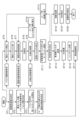
- FIG. 4 is a block diagram showing functional blocks of the laser radar device according to the first embodiment.
- FIG. 5 is a block diagram showing functional blocks of the intensity-modulated pulse generator 2 and the intensity-modulated signal generator 11 of the laser radar device according to the first embodiment.
- FIG. 6 is a block diagram showing functional blocks of the signal processing section 8 of the laser radar device according to Embodiment 1.
- FIG. 7 is a flow chart showing processing steps of the laser radar device according to the first embodiment.
- FIG. 8A is an example of a time axis graph of the received electrical signal output from the light receiving section 7.
- FIG. FIG. 8B is an example of a time-axis graph of the received electrical signal output from the integration processing section 805.
- FIG. FIG. 8 is a graph showing how the received electrical signal is processed by the signal processing unit 8 according to the first embodiment.
- FIG. 9 is an example of a graph showing the results of processing received electrical signals by the signal processing unit 8 of the laser radar device according to the first embodiment.
- FIG. 10 is a block diagram showing functional blocks of the signal processing section 8 of the laser radar device according to the second embodiment.
- FIG. 11 is a flow chart showing part of the processing steps of the laser radar device according to the second embodiment.
- the time-varying waveform of the optical electric field E having the optical frequency fc may be expressed by the following formula.
- E 0 represents the amplitude of the optical field E(t).
- the intensity modulation frequency f AM used by the technique of the present disclosure is different from the optical frequency f c in equation (1).
- the subscript AM of the intensity modulation frequency f AM is an acronym for Amplitude Modulation.
- I0 is the amplitude of the light intensity I(t) and is represented by the root mean square of the optical electric field E(t).
- the symbol ⁇ > in the formula (2) represents an operation of calculating the average value when the time is sufficiently long.
- an angular frequency ⁇ may be used instead of the frequency f.
- the relationship between the frequency f and the angular frequency ⁇ is expressed by the following equation. Note that the angular frequency ⁇ is also called angular frequency or angular velocity.
- a pulse obtained by applying intensity modulation at a certain intensity modulation frequency f AM to a light pulse of light intensity I(t) is generally called an intensity modulated pulse.
- a multi-pulse train in which several small pulses are arranged in parallel may also be used as a pseudo intensity-modulated pulse. Since this multi-pulse train can also be said to be an intensity-modulated pulse in a broad sense, it is also referred to as an intensity-modulated pulse (“intensity-modulated pulse T” in Embodiment 1) here.
- FIG. 1A is a schematic diagram showing that a laser radar device irradiates a target with laser light. Details of the target shown in FIG. 1A will become apparent from the description below.
- FIG. 1B is a graph showing transmitted light intensity and received light intensity after filtering.
- the graph at the top of FIG. 1B is a graph in which the vertical axis is transmitted light intensity and the horizontal axis is time. As shown in the graph at the top of FIG. 1B, the time interval between the first intensity-modulated pulse T1 and the second intensity-modulated pulse T2 is the repetition period Trep.
- the graph at the bottom of FIG. 1B is a graph in which the vertical axis is the received light intensity after filtering and the horizontal axis is time.
- the time interval between the first intensity-modulated pulse T1 and the first received light R1 is ⁇ T.
- ⁇ T which is the time interval between the first intensity-modulated pulse T1 and the first received light R1
- the first intensity-modulated pulse T1 is simply referred to as pulse T1
- the second intensity-modulated pulse T2 is simply referred to as pulse T2.
- FIG. 1C is a graph showing the relationship between transmitted light intensity and intensity-modulated pulse T.
- FIG. 1C is a graph in which the vertical axis is transmitted light intensity and the horizontal axis is time.
- the example shown in FIG. 1C indicates that the first intensity-modulated pulse T1 with a pulse train width ⁇ tm is composed of four pulses (P1, P2, P3, and P4) with a seed light pulse width ⁇ t.
- FIG. 1 as a whole is a schematic diagram representing an intensity modulation scheme.
- Laser radar is also called LiDAR (Light Detection and Ranging, or Laser Imaging Detection and Ranging), or (often mainly in the military domain) LADAR.
- FIG. 2A is a table summarizing the effects of varying the pulse train width ⁇ t m and the intensity modulation frequency f AM .
- the laser radar apparatus has the characteristic that the narrower the pulse train width ⁇ tm , the higher the distance resolution, and the wider the pulse train width ⁇ tm , the longer the maximum range.
- the laser radar device has the characteristic that the higher the intensity modulation frequency f AM , the higher the distance resolution, and the lower the intensity modulation frequency f AM , the longer the maximum range measurement distance.
- FIG. 2B is a table showing how the degree of matching between the signal processing filter function and the amplitude modulation envelope shape A affects the maximum ranging distance.
- the amplitude modulation envelope shape A in the table of FIG. 2 shows the relationship between the time axis and the power in the entire pulse train.
- the laser radar device has the characteristic that the maximum range measurement distance increases as the pass frequency band of the signal processing filter and the frequency components of the envelope shape A match.
- FIG. 2C is a table showing the relationship between the symmetry of the amplitude modulation envelope shape A and the maximum ranging distance. As shown in FIG. 2C, the laser radar device has the characteristic that the higher the symmetry of the envelope shape A of the amplitude modulation, the longer the maximum ranging distance.
- FIG. 2D is a table showing the correlation between each controlled variable and each parameter. More specifically, FIG. 2D shows that the intensity modulation frequency f AM can be changed by controlling the delay optical path length L Del or the seed light pulse width ⁇ t. As shown in FIG. 2D, the laser radar device has the characteristic that the pulse train width ⁇ t m or the envelope shape A can be changed by controlling the delay optical path length L Del , the seed light pulse width ⁇ t, or the number of pulse loops. be. As shown in FIG.
- the number of pulse loops may be the number of delay optical paths.
- the laser radar device according to the technology disclosed herein may be configured to be able to change each value of the delay optical path length L Del , the seed light pulse width ⁇ t, and the number of pulse loops or the number of delay optical paths by external operation.
- the user may change some or all of the delay optical path length L Del , the seed light pulse width ⁇ t, and the number of pulse loops or the number of delay optical paths by operating from the outside.
- FIG. 2 can be said to summarize the parameters that can be set by the user and the effects of manipulating the parameters for the laser radar device according to the technology disclosed herein.
- the parameters include intensity modulation frequency f AM , pulse train width ⁇ t m , and envelope shape A, as shown in FIG. 2D.
- the user may set only one of the intensity modulation frequency f AM , the pulse train width ⁇ t m , and the envelope shape A, or may set a plurality of them.
- FIG. 3 is a schematic diagram showing the hardware configuration of the signal processing unit 8 (described later) of the laser radar device according to the first embodiment.
- Each function of the signal processing unit 8 in the laser radar device is implemented by a processing circuit.
- a processing circuit even if it is dedicated hardware, is a CPU (Central Processing Unit, central processing unit, processing unit, arithmetic unit, microprocessor, microcomputer, processor, DSP (Digital Signal (also called Processor)).
- CPU Central Processing Unit
- central processing unit processing unit
- processing unit arithmetic unit
- microprocessor microcomputer
- processor DSP (Digital Signal (also called Processor)
- Processing circuitry 100a may be, for example, a single circuit, multiple circuits, a programmed processor, a parallel programmed processor, an ASIC, an FPGA, or a combination thereof.
- Each function of each part of the signal processing unit 8 may be realized by an individual processing circuit 100a, or the functions of each part may be collectively realized by one processing circuit 100a.
- FIG. 3 shows the case where each function of the signal processing unit 8 is executed by software.
- the processing circuit is a CPU such as the processor 100b
- each function of the signal processing section 8 is implemented by software, firmware, or a combination of software and firmware.
- Software and firmware are written as programs and stored in the memory 100c.
- the processing circuit implements the function of each part by reading and executing the program stored in the memory 100c. That is, when the signal processing unit 8 of the laser radar device is executed by the processing circuit, A memory 100c is provided for storing a program for executing each processing step of the signal processing unit 8 as a result. It can also be said that these programs cause a computer to execute the procedures and methods of each section of the signal processing section 8 .
- the memory 100c may be, for example, non-volatile or volatile semiconductor memory such as RAM, ROM, flash memory, EPROM, EEPROM. Also, the memory 100c may be a magnetic disk, a flexible disk, an optical disk, a compact disk, a mini disk, a DVD, or the like. Furthermore, the memory 100c may be an HDD or an SSD.
- non-volatile or volatile semiconductor memory such as RAM, ROM, flash memory, EPROM, EEPROM.
- the memory 100c may be a magnetic disk, a flexible disk, an optical disk, a compact disk, a mini disk, a DVD, or the like.
- the memory 100c may be an HDD or an SSD.
- Each function of the signal processing unit 8 of the laser radar device may be partly realized by dedicated hardware and partly realized by software or firmware.
- the processing circuit can realize each function of the signal processing section 8 of the laser radar device by hardware, software, firmware, or a combination thereof.
- FIG. 4 is a block diagram showing functional blocks of the laser radar device according to the first embodiment.
- the laser radar device includes a seed light source unit 1, an intensity-modulated pulse generator 2, a transmission-side optical system 3, a transmission/reception separation unit 4, a telescope 5, a reception-side optical system 6, A light receiving unit 7 , a signal processing unit 8 , a trigger generation circuit unit 9 , a pulse signal generation unit 10 , an intensity modulation signal generation unit 11 and a scanner 12 are provided. Arrows connecting the functional blocks shown in FIG. , the direction in which information is passed.
- Transmitted light is generated by a seed light source unit 1, and is irradiated toward an external target via an intensity-modulated pulse generator 2, a transmission-side optical system 3, a transmission/reception separation unit 4, a telescope 5, and a scanner 12. .
- the received light R reflected and received by the target is guided to the light receiving section 7 via the scanner 12 , the telescope 5 , the transmission/reception separating section 4 and the receiving side optical system 6 .
- the electrical signal shown in FIG. 4 is roughly divided into two. One is a trigger signal generated by the trigger generation circuit section 9 and a signal generated based on this trigger signal. The other is a received electric signal generated by photoelectrically converting the received light R in the light receiving section 7 .
- the seed light source unit 1 generates pulsed light. More specifically, the seed light source unit 1 includes a light source for generating a single pulse or repeatedly of pulsed light or pulsed laser. The seed light source unit 1 may generate pulsed light by Q-switching, mode locking, or pulse excitation. Further, the seed light source unit 1 may generate pulsed light by pulsing the continuous wave laser light with an optical switch. The generated pulsed light may have a single wavelength, may have a certain spread of wavelengths that cannot be called a single wavelength, or may have multiple wavelengths at the same time. The pulsed light generated by the seed light source section 1 is sent to the intensity modulated pulse generating section 2 as transmission light. The pulsed light generated by the seed light source unit 1 has a variable seed light pulse width. The seed light source unit 1 generates pulse light based on a pulse signal from a pulse signal generation unit 10, which will be described later.
- the trigger generation circuit unit 9 generates a trigger signal (hereinafter referred to as a “pulse irradiation trigger signal”) that gives the timing of irradiating the pulsed light.
- the trigger generation circuit section 9 may be implemented by, for example, a pulse generator, a function generator, or an FPGA.
- the pulse irradiation trigger signal generated by the trigger generation circuit section 9 is sent to the signal processing section 8, the pulse signal generation section 10, and the intensity modulated signal generation section 11.
- the pulse signal generator 10 generates a pulse signal based on the pulse irradiation trigger signal sent.
- the pulse signal generator 10 may also be realized by, for example, a pulse generator, a function generator, or an FPGA. A pulse signal generated by the pulse signal generating section 10 is sent to the seed light source section 1 .
- the intensity modulated signal generator 11 generates an intensity modulated signal. More specifically, the intensity-modulated signal generator 11 generates an intensity-modulated signal based on the transmitted pulse irradiation trigger signal.
- the intensity-modulated signal generator 11 may also be implemented by, for example, a pulse generator, function generator, or FPGA.
- the intensity-modulated signal generated by the intensity-modulated signal generator 11 is sent to the intensity-modulated pulse generator 2 .
- the details of the function of the intensity-modulated signal generator 11 will become clear from the explanation along FIG. 5 below.
- the intensity-modulated pulse generator 2 generates intensity-modulated pulsed light based on the transmitted pulsed light and intensity-modulated signal.
- the intensity-modulated pulsed light generated by the intensity-modulated pulse generator 2 is sent to the transmission-side optical system 3 .
- the details of the function of the intensity-modulated pulse generator 2 will become clear from the explanation along FIG. 5 below.
- the transmission-side optical system 3 shapes the series of intensity-modulated pulsed light beams sent from the intensity-modulated pulse generator 2 (hereinafter referred to as "intensity-modulated pulse train") into a beam diameter and spread angle that match the design specifications. do.
- the transmission-side optical system 3 is preferably composed of a lens group including a concave lens and a convex lens.
- the transmission-side optical system 3 may include a reflective optical system using a mirror.
- the purpose of the transmission-side optical system 3 to shape the beam diameter and divergence angle of the intensity-modulated pulse train is to increase the SNR (Signal Noise Ratio). Therefore, if the intensity-modulated pulse train has an SNR that satisfies the design specifications without shaping the intensity-modulated pulse train, the transmitting optical system 3 may simply be the path of the intensity-modulated pulse train.
- optical amplification, wavelength conversion, optical amplification, wavelength conversion, and an optical system for performing operations on the pulsed light such as frequency shift.
- the transmission/reception separation unit 4 is a separator that separates the transmission light and the reception light R into respective ports.
- the transmission/reception separation unit 4 can be realized by a polarization beam splitter or a circulator.
- the transmission/reception separation unit 4 can be realized as a polarization beam splitter arranged on the optical axis between the transmission side optical system 3 and the telescope 5 .
- the transmission/reception separation unit 4 can be realized by a circulator.
- the transmission light that has passed through the transmission/reception separation unit 4 is sent to the telescope 5 .
- the received light R that has passed through the transmission/reception separation unit 4 is sent to the reception side optical system 6 .
- the term telescope means a telescope.
- the telescope 5 of the laser radar device according to Embodiment 1 is a component having the same structure as a telescope.
- the telescope 5 may consist of a lens group including a concave lens and a convex lens.
- the telescope 5 may also include a reflective optical system using mirrors.
- the transmitted light that has passed through the telescope 5 is sent to the scanner 12 .
- the received light R that has passed through the telescope 5 is sent to the transmission/reception separation section 4 .
- the scanner 12 is, for example, a galvanometer scanner, and may be a galvanometer mirror attached to a galvanometer motor.
- a galvanomirror is also called a scan mirror or a scanner mirror.
- Scanner 12 is controlled so that the transmitted light is directed toward the target.
- the received light R reflected and received by the target is sent to the light receiving section 7 via the scanner 12 , the telescope 5 , the transmission/reception separation section 4 and the reception side optical system 6 .
- the receiving optical system 6 shapes the received light R, which has passed through the transmission/reception separating section 4, into a beam diameter and a divergence angle that meet design specifications.
- the receiving optical system 6 is preferably composed of a lens group consisting of a concave lens and a convex lens.
- the receiving optical system 6 may include a reflective optical system using a mirror.
- the purpose of shaping the beam diameter and divergence angle of the received light R by the receiving optical system 6 is to increase the SNR. Therefore, if the received light R has an SNR that satisfies the design specifications without shaping the received light R, the receiving optical system 6 may simply be the path of the received light R.
- FIG. 8A shows an example of a time-axis graph of the received electrical signal output from the light receiving section 7.
- FIG. The vertical axis of the graph shown in FIG. 8A represents the voltage of the received electrical signal, and is labeled as "received signal voltage".
- FIG. 5 is a block diagram showing functional blocks of the intensity-modulated pulse generator 2 and the intensity-modulated signal generator 11 of the laser radar device according to the first embodiment.
- the intensity-modulated pulse generator 2 and the intensity-modulated signal generator 11 are functional blocks that perform intensity modulation on transmission light.
- the intensity-modulated pulse generator 2 includes an optical path coupling section 201 , a variable branching ratio optical path branching section 202 , and a delay optical path section 203 .
- the intensity modulated signal generator 11 includes a branching ratio adjuster 1101 and a delay optical path adjuster 1102 .
- the optical path coupling section 201, the branching ratio variable optical path branching section 202, and the delay optical path section 203 in the intensity modulated pulse generating section 2 are coupled in a loop.
- Optical path coupling section 201 receives the light from seed light source section 1 and the light from delay optical path section 203 , and outputs the combined light to branching ratio variable optical path branching section 202 .
- the optical path coupling section 201 may be implemented by, for example, a coupler or a polarization beam splitter.
- the branching ratio variable optical path branching unit 202 outputs one branched light to the transmission side optical system 3 and the remaining branched light to the delay optical path unit 203 based on a branching ratio adjustment signal described later.
- the branching ratio variable optical path branching section 202 receives the light from the optical path coupling section 201 and outputs the branched light to the delay optical path section 203 and the transmission side optical system 3 .
- the branching ratio variable optical path branching unit 202 may be realized by appropriately combining a phase modulator, a Pockels cell, an optical wavelength plate, and a polarizing beam splitter.
- the branching ratio variable optical path branching unit 202 acquires the branching ratio adjustment signal from the branching ratio adjustment unit 1101 and adjusts the branching ratio based on the branching ratio adjustment signal.
- the delay optical path section 203 is for adjusting the phase difference between the two lights coupled by the optical path coupling section 201, and may be implemented by mirrors, fibers, or the like.
- the degree of delay or the optical delay length L Del of the optical delay path section 203 changes according to a control signal from the optical delay adjustment section 1102, which will be described later.
- a branching ratio adjusting section 1101 in the intensity modulated signal generating section 11 outputs a branching ratio adjusting signal that determines the branching ratio in the variable branching ratio optical path branching section 202 . More specifically, the branching ratio adjustment unit 1101 generates a branching ratio adjustment signal, which is a control signal for adjusting the branching ratio in the variable branching ratio optical path branching unit 202, and controls the variable branching ratio optical path branching unit 202. .
- the delay optical path adjustment unit 1102 in the intensity modulated signal generation unit 11 generates a control signal (hereinafter referred to as "delay optical path control signal") for adjusting the degree of delay or the delay optical path length L Del in the delay optical path unit 203, It controls the delay optical path section 203 .
- FIG. 6 is a block diagram showing functional blocks of the signal processing section 8 of the laser radar device according to Embodiment 1.
- the signal processing unit 8 includes a filter processing unit 801, an analog-digital conversion unit (A/D conversion unit) 802, a range bin dividing unit 803, a frequency analysis unit 804, an integration processing unit 805, A functional block composed of an SNR calculator 806 and a distance characteristic calculator 807 is provided in a form in which these are serially connected in order.
- a functional block composed of an SNR calculator 806 and a distance characteristic calculator 807 is provided in a form in which these are serially connected in order.
- a filter processing unit 801 of the signal processing unit 8 filters the received electrical signal from the light receiving unit 7 .
- Filter processing unit 801 is specifically a bandpass filter.
- Filtering section 801 performs filtering based on the intensity-modulated signal from intensity-modulated signal generating section 11 . Note that FIG. 4 does not show an arrow from the block of the intensity-modulated signal generator 11 to the block of the signal processor 8, but this is simply because priority is given to the visibility of the entire drawing.
- the analog-to-digital converter 802 of the signal processor 8 converts the filtered analog electrical signal from the filter processor 801 into a digital electrical signal.
- the analog-to-digital conversion unit 802 performs AD conversion processing based on the pulse irradiation trigger signal from the trigger generation circuit unit 9 .
- the range bin dividing unit 803 of the signal processing unit 8 divides the digital electric signal, which is the output of the analog-to-digital converting unit 802, in the time direction by a width corresponding to the pulse width.
- the range bin division unit 803 performs range bin division processing based on the pulse irradiation trigger signal from the trigger generation circuit unit 9 .
- the range bins are equal intervals of the horizontal time axis, and in the example of FIG. is represented.
- the frequency analysis unit 804 of the signal processing unit 8 performs fast Fourier transform (FFT) on the signals for each bin after range bin division processing.
- the signal for each bin is transformed into a spectrum for each bin by applying a fast Fourier transform.
- a frequency analysis unit 804 performs fast Fourier transform based on the intensity-modulated signal from the intensity-modulated signal generation unit 11 .
- the integration processing unit 805 of the signal processing unit 8 integrates a plurality of spectra obtained from a plurality of shots of data of the same frequency in spectral space.
- the integration process has the same effect as the averaging process, and can be expected to improve the SNR.
- FIG. 8B is an example of a time-axis graph of the received electrical signal output from the integration processing section 805.
- FIG. FIG. 8B is a graph showing how the received electrical signal is processed in the signal processing unit 8 according to Embodiment 1 by comparison with FIG. 8A. In the graph shown in FIG. 8A, a faint peak reflecting the scattered light from the target can be confirmed in the region where the range bin label n is 3.
- the SNR calculator 806 of the signal processor 8 calculates the SNR of the received electrical signal.
- the SNR calculator 806 calculates the SNR for each range bin.
- the distance characteristic calculator 807 of the signal processor 8 calculates the relationship between distance and SNR (hereinafter referred to as "distance characteristic") for each intensity modulation frequency fAM .
- the distance characteristic is displayed with the SNR on the vertical axis and the distance on the horizontal axis in the same way as A-scope, which displays the waveform with the received signal strength on the vertical axis and the distance on the horizontal axis. be able to.
- FIG. 9 is an example of a graph representing distance characteristics in the A-scope style. It can be said that FIG. 9 represents the result of processing the received electrical signal by the signal processing unit 8 .
- the distance, which is the horizontal axis of the graph shown in FIG. 9, is merely obtained according to the principle of TOF. ⁇ t shown in FIG.
- FIG. 7 is a flow chart showing processing steps of the laser radar device according to the first embodiment. As shown in FIG. 7, the processing steps of the laser radar device include steps ST1 to ST20.
- the laser radar device measures a target in a medium having a strong scattering property such as water fog or dust.
- a substance having a strong scattering property such as water mist or dust is called a "volume target”
- a measurement object in the volume target is called a "hard target” to distinguish between the two.
- the difference between volume targets and hard targets can also be expressed by differences in the behavior of scattered light. That is, a large number of volume targets exist within a certain spatial distribution, and are targets that are received by superimposing the scattered light at each spatial position on the transmission light coordinate axis.
- a hard target is a target in which light is diffused or reflected on a light receiving surface and scattered light is not superimposed.
- Step ST1 is a step in which the laser radar device assists the user in determining the intensity modulation frequency f AM .
- the intensity modulation frequency f AM should be determined in consideration of the characteristics of the volume target. More specifically, the intensity modulation frequency f AM is preferably determined in consideration of the extinction coefficient and refractive index of the volume target.
- the intensity modulation frequency f AM of the laser radar device according to the first embodiment may be time-invariant, or may be time-varying like a chirp frequency.
- the intensity modulation frequency f AM may be a single frequency or a mixed frequency having a plurality of frequencies.
- the laser radar device according to the technology disclosed herein has a display (not shown), and displays information for determining the intensity modulation frequency f AM to the user of the laser radar device. Further, the laser radar device according to the technology disclosed herein is provided with a keyboard, mouse, etc. (not shown), and is programmed so that the intensity modulation frequency f AM determined by the user can be input to the laser radar device.
- Step ST2 is a step in which the laser radar device assists the user in determining the seed light pulse width .delta.t, the envelope shape A, and the pulse train width .delta.tm .
- the envelope shape A indicates the relationship between the time axis and the power in the entire pulse train.
- the seed light pulse width ⁇ t, the envelope shape A, and the pulse train width ⁇ t m are based on the intensity modulation frequency f AM determined in step ST1 and design specifications such as the filter characteristics, spectral width, and distance resolution of the filter processing unit 801. , should be determined.
- the laser radar device displays on the display the intensity modulation frequency f AM determined in step ST1 and design specifications such as filter characteristics, spectrum width, and distance resolution in the filter processing section 801 . Further, the laser radar device according to the technique of the present disclosure is programmed so that the user-determined seed light pulse width ⁇ t, envelope shape A, and pulse train width ⁇ tm can be input to the laser radar device.
- the pulse train width ⁇ tm is preferably determined taking into consideration the delay optical path length L Del in the delay optical path section 203 of the intensity modulated pulse generator 2 as well.
- the delay optical path length L Del in the delay optical path section 203 of the intensity modulated pulse generator 2 is equal to the distance traveled by light in the period (1/f AM ) of the intensity modulated signal as follows.
- c represents the speed of light.
- the pulse train width ⁇ tm may satisfy the following relational expression.
- Step ST3 is a step in which the laser radar apparatus discretizes the envelope shape A of the pulse and calculates the design value of the optical power of each pulse constituting the pulse train.
- the number of pulses constituting a pulse train is M.
- a pulse that passes through the branching ratio variable optical path branching unit 202 for the k-th time (k is any number from 1 to M) and is output to the transmission side optical system 3 is referred to as a k -th pulse Pk.
- the number of loops in the intensity modulated pulse generator 2 is M-1. That is, step ST3 represents a process of calculating the design value of the optical power for each of the pulses (P 1 , P 2 , . . . P M ) during the loop time in the intensity modulated pulse generator 2 .
- Step ST4 is a processing step performed by the branching ratio adjusting section 1101 .
- the branching ratio adjusting section 1101 calculates the branching ratio in the variable branching ratio optical path branching section 202.
- FIG. Specifically, the branching ratio adjusting unit 1101 calculates the branching ratio of the k-th loop in the variable branching ratio optical path branching unit 202 based on the following equation.
- the script typeface P in equation (6) represents the optical power.
- a script typeface P with a subscript k represents the optical power of the kth pulse Pk .
- the script typeface P with the subscript out indicates the optical power of the light output to the transmission side optical system 3 .
- the script typeface P with the subscript loop indicates the optical power of the light output to the delay optical path section 203 . That is, equation (6) is obtained by dividing the branching ratio of the k-th loop in the branching ratio variable optical path branching unit 202 by the branching ratio adjusting unit 1101, the k -th pulse P in the pulse train, and the optical power of the k-th pulse in the pulse train. , and the sum of the optical powers of the pulses from to the end. By adopting the branching ratio shown in Equation (6), the optical power of the light output to the transmission side optical system 3 becomes equal to the design value of the optical power calculated in step ST3.
- Step ST4 also includes a step of generating a branching ratio adjustment signal for setting the branching ratio of variable branching ratio optical path branching section 202 to the value shown in equation (6).
- Step ST4 also includes a step of generating a delay optical path control signal for adjusting the delay optical path section 203 .
- Step ST5 is a processing step performed by the pulse signal generator 10 .
- the pulse signal generator 10 controls the seed light source 1 based on the pulse irradiation trigger signal.
- the seed light source unit 1 controlled by the pulse signal generation unit 10 generates light pulses having a repetition period T rep and a seed light pulse width ⁇ t .
- the upper part of FIG. 1B shows that an optical pulse having a seed light pulse width ⁇ t is generated for each repetition period T rep .
- Step ST6 is a processing step performed by the seed light source section 1.
- the seed light source section 1 outputs the generated light pulse to the intensity modulated pulse generation section 2 .
- Step ST7 is a processing step performed by the delay optical path adjustment section 1102 .
- the delay optical path adjustment section 1102 controls the optical path length of the delay optical path section 203 .
- Step ST8 is a processing step performed by the optical path coupling section 201 .
- the optical path coupling section 201 couples the light from the seed light source section 1 and the light from the delay optical path section 203.
- the optical path coupling section 201 outputs the coupled light to the branching ratio variable optical path branching section 202.
- Step ST9 is a processing step performed by the branching ratio variable optical path branching unit 202 .
- the branching ratio variable optical path branching unit 202 outputs one branched light to the transmission side optical system 3 and the remaining branched light to the delay optical path unit 203 based on the branching ratio adjustment signal.
- the light branched to the delay optical path section 203 is sent to the optical path coupling section 201 after propagating the designed delay optical path length L Del .
- Step ST10 indicates that the process from steps ST7 to ST9 is a loop process repeated M times.
- the intensity-modulated pulse generator 2 converts the light pulse generated by the seed light source 1 into an intensity-modulated light pulse (or simply an "intensity-modulated pulse T”), and outputs it to the transmission side optical system 3 .
- T intensity-modulated light pulse
- the letter T used here is derived from the English word Transmitter, which means a transmitter.
- the subscript attached to T is simply a serial number that changes from 1 to 2 in chronological order (see FIG. 1B).
- Step ST11 is a processing step performed by the telescope 5 and the scanner 12.
- the telescope 5 outputs an intensity-modulated pulse T (for example, m-th intensity-modulated pulse T m ) to the scanner 12 .
- the scanner 12 rotates the scanner mirror so that the intensity-modulated pulse T is emitted toward the target.
- the irradiated intensity-modulated pulse T is irradiated toward a hard target existing within the volume target, and received light R is generated by reflection and scattering.
- the letter R used here is derived from the English word Receiver, which means a receiver.
- the subscript attached to R (for example, m of the m-th received light Rm) is a serial number that similarly changes from 1 to 2 in chronological order (see FIG. 1B).
- Step ST12 is a processing step performed by the telescope 5, the scanner 12, and the transmission/reception separating unit 4, the receiving optical system 6, and the light receiving unit 7, which are functional blocks on the receiving side.
- the telescope 5 outputs the received light R (for example, the first received light R 1 ) to the transmission/reception separating section 4 .
- Step ST12 includes a step in which the transmission/reception separation section 4 outputs the received light R to the receiving side optical system 6, a step in which the receiving side optical system 6 processes the received light R, and a step in which the receiving side optical system 6 and outputting the received light R that has passed through to the light receiving unit 7 .
- step ST12 includes a step of converting the received light R into a received electric signal by the light receiving unit 7 and a step of outputting the received electric signal to the signal processing unit 8 by the light receiving unit 7 .
- Step ST13 indicates that the process from steps ST5 to ST12 is a loop process that is repeated a times.
- a is the pulse integration count a.
- the pulse integration count a is a design parameter that determines the SNR of the laser radar device.
- the laser radar device according to the technology disclosed herein may have a configuration in which a screen for initial setting is displayed on the display, and the user can freely set the pulse integration count a in the initial setting.
- Steps ST14 to ST17 are processing steps performed by the signal processing unit 8, but the laser radar device may perform the processing sequentially, or the loop processing of steps ST5 to ST12, which is repeated a times, is completed. You can wait for and process it all at once.
- Step ST14 is a processing step performed by the filter processing section 801 .
- the filtering section 801 filters the received electrical signal based on the intensity-modulated signal from the intensity-modulated signal generating section 11.
- FIG. Note that the frequency of the intensity-modulated signal is represented by the symbol f AM used in equation (4).
- Step ST15 is a processing step performed by the analog-to-digital converter 802 .
- the analog-to-digital converter 802 converts the received analog electrical signal corresponding to the received light R into a digital signal.
- the digital conversion processing performed by the analog-to-digital conversion unit 802 is triggered by a pulse irradiation trigger signal from the trigger generation circuit unit 9 . That is, the start time of the digital conversion processing performed by the analog-to-digital conversion unit 802 theoretically matches the timing at which the pulsed light is irradiated.
- the digital conversion processing performed by the analog-to-digital converter 802 continues for a predetermined time or until the next pulsed light is emitted.
- the signal that is digitally converted after ⁇ T from the start of digital conversion, i.e., the irradiation of the pulsed light, is reflected by the target at a distance (L) shown in the following formula, according to the principle of TOF. I know it's a thing.
- the length unit for digital conversion of the received electric signal may be one pulse.
- Step ST16 is a processing step performed by the range bin dividing section 803 .
- the range bin dividing section 803 divides the digitally converted received electrical signal into signals for each range bin.
- FIG. 8A is a time-axis graph representing the k-th received light Rk that is irradiated with one pulse, for example, the k-th pulse Pk , is reflected by the target, and is input to the laser radar device.
- n shown in FIG. 8A is a label attached to the range bin, and the smaller the range bin label n, the closer the target is to the laser radar device.
- the range bin width, ie, the time interval ⁇ t from the start to the end of one range bin may be equal to the seed light pulse width ⁇ t.
- the laser radar device may be programmed so that design parameters including the seed light pulse width ⁇ t determined by the user can be input to the laser radar device.
- Step ST17 is a processing step performed by frequency analysis section 804 .
- frequency analysis section 804 Fourier-transforms each of the received signals divided for each range bin to calculate a spectrum. Further, in step ST17, frequency analysis section 804 outputs the calculated spectrum to integration processing section 805.
- FIG. the intensity modulation frequency f AM of the laser radar device may be time-invariant or may be time-variant such as the chirp frequency. That is, the intensity modulation frequency f AM may differ from pulse to pulse.
- the intensity-modulated frequency f AM of the m -th intensity-modulated pulse Tm is distinguished by being represented as the m-th intensity-modulated frequency f AM_m .
- the spectrum obtained by the Fourier transform of the digitally converted received electrical signal of the mth received light Rm has a peak frequency that approximately matches the mth intensity modulation frequency fAM_m . Strictly speaking , frequency shift may occur due to the movement of the target. no problem.
- Step ST18 is a processing step performed by the integration processing unit 805.
- the integration processing section 805 integrates the transmitted spectrum for the number of pulse integration times a.
- Step ST19 is a processing step performed by the SNR calculation unit 806.
- SNR calculation section 806 calculates the ratio of peak intensity to out-of-band noise, and sets this as the SNR of the spectrum. The calculation of the ratio of peak intensity to out-of-band noise is performed for each range bin.
- SNR calculation section 806 outputs the integrated spectrum and the SNR for each range bin to distance characteristic calculation section 807 .
- Step ST20 is a processing step performed by the distance characteristic calculation unit 807.
- the distance characteristic calculation section 807 converts the sent SNR information for each range bin into SNR information for each distance.
- the range bins in the technique of the present disclosure have physical units of time (also referred to as "dimensions"). Conversion of the unit of time to the unit of distance may be performed according to the principle of TOF.
- the laser radar apparatus according to Embodiment 1 is configured to include the branching ratio variable optical path branching unit 202 and the branching ratio adjusting unit 1101, the operational effect is that the amplitude modulation envelope shape A can be changed by an external operation.
- the laser radar apparatus according to Embodiment 1 is configured to include the intensity-modulated pulse generator 2 composed of the optical path coupling section 201, the branching ratio variable optical path branching section 202, and the delay optical path section 203.
- the envelope shape A of the amplitude modulation can be deformed by an external operation.
- the laser radar apparatus is configured to include the intensity-modulated pulse generator 2 composed of the optical path coupling unit 201, the branching ratio variable optical path branching unit 202, and the delay optical path unit 203, the intensity modulation frequency f It has the effect of making AM variable. Since the laser radar device according to Embodiment 1 has the above effects, it has the effect of being able to freely adjust the range resolution and the maximum range-finding distance according to the purpose of range-finding.
- Embodiment 2 clarifies some modifications of the laser radar device described in Embodiment 1. FIG.
- the laser radar device may be a coherent lidar, a differential absorption lidar, or a dual polarization lidar.
- the laser radar device can measure not only target position information but also target speed information. If the laser radar system is a differential absorption lidar, the components of the laser radar system are slightly different from those in the first embodiment.
- the seed light source unit 1 In the laser radar device when it is a differential absorption lidar, the seed light source unit 1 generates a first intensity-modulated pulse with a first wavelength and a second intensity-modulated pulse with a second wavelength different from the first wavelength. Output.
- the signal processing unit 8 calculates the intensity ratio of received signals corresponding to the first intensity-modulated pulse and the second intensity-modulated pulse.
- the laser radar device in the case of a differential absorption lidar can measure the absorption wavelength and concentration of the target in addition to the position information of the target.
- the components of the laser radar system are slightly different from those in the first embodiment.
- the seed light source unit 1 outputs intensity-modulated pulses in two orthogonal polarization states.
- the signal processing unit 8 calculates the intensity ratio of the received signals corresponding to the two orthogonal polarizations.
- the laser radar device in the case of a differential absorption lidar can measure the grain shape of the target in addition to the positional information of the target.
- the laser radar device according to the technology disclosed herein is not limited to this.
- the laser radar device according to the technology disclosed herein may have a configuration in which the telescopes 5 are separately provided for transmission and reception.
- the laser radar device performs measurements a plurality of times while changing the parameters of the pulse train used by the laser radar device (hereinafter referred to as "pulse train parameters")
- a feedback mechanism may be provided to optimize the pulse train parameters by comparing the measurements. Pulse train parameters may be optimized, for example, to improve the SNR of received signals from hard targets. Alternatively, the pulse train parameters may be optimized by comparing the SNR of the hard target and the SNR of the volume target so that the difference is large.
- FIG. 10 is a block diagram showing functional blocks of the signal processing section 8 of the laser radar device according to the second embodiment.
- FIG. 11 is a flow chart showing part of the processing steps of the laser radar device according to the second embodiment.
- the functional block of the SNR comparator 808 shown in FIG. 10 performs a processing step of comparing the SNRs of a plurality of measurements made while varying the pulse train parameters.
- FIG. 10 shows that the information of the pulse train parameters, which is obtained by the SNR comparing section 808 and is regarded as appropriate, is fed back to the pulse signal generating section 10 and the intensity modulated signal generating section 11 .
- Step ST21 shown in FIG. 11 is this processing step performed by the SNR comparator 808.
- the laser radar device according to the second embodiment is several modifications of the laser radar device described in the first embodiment.
- the laser radar device according to Embodiment 2 has the effects clarified in Embodiment 1, and can freely adjust the distance resolution and the maximum ranging distance according to the purpose of ranging. It has the effect of
- the laser radar device can be applied to range finding of hard targets among volume targets, and has industrial applicability.
- 1 type light source unit 2 intensity modulation pulse generation unit, 3 transmission side optical system, 4 transmission/reception separation unit, 5 telescope, 6 reception side optical system, 7 light receiving unit, 8 signal processing unit, 9 trigger generation circuit unit, 10 pulse Signal generating section 11 Intensity modulated signal generating section 12 Scanner 100a Processing circuit 100b Processor 100c Memory 201 Optical path coupling section 202 Branching ratio variable optical path branching section 203 Delay optical path section 801 Filtering section 802 Analog digital Conversion unit 803 Range bin division unit 804 Frequency analysis unit 805 Integration processing unit 806 SNR calculation unit 807 Distance characteristic calculation unit 808 SNR comparison unit 1101 Branching ratio adjustment unit 1102 Delay optical path adjustment unit.
Landscapes
- Engineering & Computer Science (AREA)
- Computer Networks & Wireless Communication (AREA)
- Physics & Mathematics (AREA)
- General Physics & Mathematics (AREA)
- Radar, Positioning & Navigation (AREA)
- Remote Sensing (AREA)
- Optical Radar Systems And Details Thereof (AREA)
Abstract
A laser radar device according to the present disclosure comprises a seed light source unit (1) for generating pulse light, an intensity-modulated signal generation unit (11) for generating an intensity-modulated signal, and an intensity-modulated pulse generation unit (2) for generating intensity-modulated pulse light on the basis of the pulse light and the intensity-modulated signal. The intensity-modulated signal generation unit (11) has a branch ratio adjustment unit (1101) and a delay light path adjustment unit (1102). The intensity-modulated pulse generation unit (2) has a light path linking unit (201), a variable-branch-ratio light path branching unit (202), and a delay light path unit (203) that are linked in the form of a loop. The branch ratio adjustment unit (1101) outputs a branch ratio adjustment signal for determining the branch ratio in the variable-branch-ratio light path branching unit (202). The variable-branch-ratio light path branching unit (202) outputs some of the branched light to a transmission-side optical system (3), and outputs the remaining branched light to the delay light path unit (203), on the basis of the branch ratio adjustment signal.
Description
本開示技術はレーザレーダ装置に関する。
The technology disclosed herein relates to a laser radar device.
レーザレーダの技術分野において、TOF(Time of Flight)の原理を用いて測距する技術が知られている。またTOFに用いる送信光に、強度変調パルスを用いる方式(以降、「強度変調パルス版TOF方式」と称する)も知られている。
In the technical field of laser radar, a technique for measuring distances using the principle of TOF (Time of Flight) is known. There is also known a method of using an intensity-modulated pulse for transmission light used for TOF (hereinafter referred to as an "intensity-modulated pulse version TOF method").
例えば非特許文献1には、強度変調パルス版TOF方式に係る技術が開示されている。
For example, Non-Patent Document 1 discloses a technique related to an intensity-modulated pulse version TOF method.
強度変調パルス版TOF方式を採用するレーザレーダ装置において、測距の目的に応じて、最大測距距離又は距離分解能を自由に外部からの操作により変えたい、という要望がある。本開示技術は、この課題を解決するものであり、測距の目的に応じて最大測距距離又は距離分解能を外部からの操作により変えることができるレーザレーダ装置を提供することを目的とする。
In a laser radar device that employs an intensity-modulated pulse version TOF method, there is a demand to freely change the maximum ranging distance or range resolution by external operation according to the purpose of ranging. The technique disclosed herein solves this problem, and an object thereof is to provide a laser radar device capable of changing the maximum range-finding distance or range resolution by external operation according to the purpose of range-finding.
本開示技術に係るレーザレーダ装置は、パルス光を生成する種光源部と、強度変調信号を生成する強度変調信号生成部と、パルス光及び強度変調信号に基づいて、強度変調パルス光を生成する強度変調パルス生成部と、を備える。強度変調信号生成部は、分岐比調整部と、遅延光路調整部と、を有し、強度変調パルス生成部は、ループ状に結合された、光路結合部と、分岐比可変光路分岐部と、遅延光路部と、を有し、分岐比調整部は、分岐比可変光路分岐部における分岐比を決定する分岐比調整信号を出力し、分岐比可変光路分岐部は、分岐比調整信号に基づいて、分岐された一方の光を送信側光学系へ、分岐された残りの光を遅延光路部へ、それぞれ出力する。
A laser radar device according to the technology disclosed herein includes a seed light source unit that generates pulsed light, an intensity-modulated signal generation unit that generates an intensity-modulated signal, and an intensity-modulated pulsed light that is generated based on the pulsed light and the intensity-modulated signal. an intensity-modulated pulse generator. The intensity-modulated signal generator includes a branching ratio adjusting unit and a delay optical path adjusting unit, and the intensity-modulated pulse generating unit includes an optical path coupling unit, a variable branching ratio optical path branching unit, and a looped optical path coupling unit. and a delay optical path section, the branching ratio adjusting section outputs a branching ratio adjustment signal that determines the branching ratio in the variable branching ratio optical path branching section, and the variable branching ratio optical path branching section is based on the branching ratio adjustment signal. , one branched light is output to the transmission side optical system, and the remaining branched light is output to the delay optical path section.
本開示技術に係るレーザレーダ装置は、分岐比可変光路分岐部及び分岐比調整部を備える構成であるため、振幅変調の変調周波数、パルス列幅、及び振幅変調の包絡線形状を外部からの操作により変えることができる。振幅変調の変調周波数、パルス列幅、及び振幅変調の包絡線形状を外部からの操作により変えることにより本開示技術に係るレーザレーダ装置は、測距の目的に応じて最大測距距離又は距離分解能を外部からの操作により変えることができる。
Since the laser radar device according to the technology disclosed herein is configured to include the branching ratio variable optical path branching unit and the branching ratio adjusting unit, the modulation frequency of the amplitude modulation, the pulse train width, and the envelope shape of the amplitude modulation can be controlled from the outside. can change. By changing the modulation frequency of amplitude modulation, the pulse train width, and the envelope shape of amplitude modulation by external operation, the laser radar device according to the technology of the present disclosure can increase the maximum ranging distance or range resolution according to the purpose of ranging. It can be changed by an external operation.
一般に、光周波数fcをもつ光電場Eの時間変化波形は、以下の数式で表現されることがある。

ここでE0は、光電場E(t)の振幅を表す。
本開示技術が用いる強度変調周波数fAMは、式(1)における光周波数fcとは異なるものである。

強度変調周波数fAMの下添え字のAMは、振幅変調を意味するAmplitude Modulationの頭文字である。ここでI0は、光強度I(t)の振幅であって、光電場E(t)の二乗平均で表される。式(2)における<>の記号は、時間を十分長くとったときの平均値を算出する操作を表す。
周波数特性を表示する場合、周波数fの代わりに角周波数ωを用いることがある。周波数fと角周波数ωとの関係は、以下の式のとおりである。

なお角周波数ωは、角振動数、又は角速度とも称される。 In general, the time-varying waveform of the optical electric field E having the optical frequency fc may be expressed by the following formula.
where E 0 represents the amplitude of the optical field E(t).
The intensity modulation frequency f AM used by the technique of the present disclosure is different from the optical frequency f c in equation (1).
The subscript AM of the intensity modulation frequency f AM is an acronym for Amplitude Modulation. Here, I0 is the amplitude of the light intensity I(t) and is represented by the root mean square of the optical electric field E(t). The symbol <> in the formula (2) represents an operation of calculating the average value when the time is sufficiently long.
When displaying frequency characteristics, an angular frequency ω may be used instead of the frequency f. The relationship between the frequency f and the angular frequency ω is expressed by the following equation.
Note that the angular frequency ω is also called angular frequency or angular velocity.
ここでE0は、光電場E(t)の振幅を表す。
本開示技術が用いる強度変調周波数fAMは、式(1)における光周波数fcとは異なるものである。
強度変調周波数fAMの下添え字のAMは、振幅変調を意味するAmplitude Modulationの頭文字である。ここでI0は、光強度I(t)の振幅であって、光電場E(t)の二乗平均で表される。式(2)における<>の記号は、時間を十分長くとったときの平均値を算出する操作を表す。
周波数特性を表示する場合、周波数fの代わりに角周波数ωを用いることがある。周波数fと角周波数ωとの関係は、以下の式のとおりである。
なお角周波数ωは、角振動数、又は角速度とも称される。 In general, the time-varying waveform of the optical electric field E having the optical frequency fc may be expressed by the following formula.
where E 0 represents the amplitude of the optical field E(t).
The intensity modulation frequency f AM used by the technique of the present disclosure is different from the optical frequency f c in equation (1).
The subscript AM of the intensity modulation frequency f AM is an acronym for Amplitude Modulation. Here, I0 is the amplitude of the light intensity I(t) and is represented by the root mean square of the optical electric field E(t). The symbol <> in the formula (2) represents an operation of calculating the average value when the time is sufficiently long.
When displaying frequency characteristics, an angular frequency ω may be used instead of the frequency f. The relationship between the frequency f and the angular frequency ω is expressed by the following equation.
Note that the angular frequency ω is also called angular frequency or angular velocity.
光強度I(t)の光パルスに対して、或る強度変調周波数fAMで強度変調が加えられたパルスは、一般に強度変調パルスと称される。また、いくつかの小パルスが並列に並べられたマルチパルス列も、擬似的に強度変調パルスとして利用されることがある。このマルチパルス列も、広義の意味で強度変調パルスだと言えるため、ここではこれも強度変調パルス(実施の形態1においては、「強度変調パルスT」)と称する。
A pulse obtained by applying intensity modulation at a certain intensity modulation frequency f AM to a light pulse of light intensity I(t) is generally called an intensity modulated pulse. A multi-pulse train in which several small pulses are arranged in parallel may also be used as a pseudo intensity-modulated pulse. Since this multi-pulse train can also be said to be an intensity-modulated pulse in a broad sense, it is also referred to as an intensity-modulated pulse (“intensity-modulated pulse T” in Embodiment 1) here.
実施の形態1.
図1Aは、レーザレーダ装置がターゲットに対してレーザ光を照射していることを示す模式図である。図1Aに示されるターゲットの詳細は、後述の説明により明らかとなる。
図1Bは、送信光強度とフィルタ処理後の受信光強度とを示すグラフである。図1Bの上部にあるグラフは、縦軸を送信光強度とし、横軸を時間としたグラフである。図1Bの上部にあるグラフに示されるとおり、1番目強度変調パルスT1と2番目強度変調パルスT2との時間間隔は、繰返し周期Trepである。図1Bの下部にあるグラフは、縦軸をフィルタ処理後の受信光強度とし、横軸を時間としたグラフである。図1Bの上部のグラフと下部のグラフに示されるとおり、1番目強度変調パルスT1と1番目受信光R1との時間間隔は、ΔTである。1番目強度変調パルスT1と1番目受信光R1との時間間隔であるΔTは、光が照射されてから、ターゲットで反射され、受信されるまで、の時間である。なお図1Bにおいてはスペースの制限から、1番目強度変調パルスT1は単にパルスT1と、2番目強度変調パルスT2は単にパルスT2と、省略して記載がなされている。
図1Cは、送信光強度と強度変調パルスTとの関係を示すグラフである。図1Cに示されているグラフは、縦軸を送信光強度とし、横軸を時間としたグラフである。図1Cに示される例では、パルス列幅δtmの1番目強度変調パルスT1が、種光パルス幅δtの4つのパルス(P1、P2、P3、及びP4)から構成されていることを示している。
全体として図1は、強度変調方式を表す模式図である。レーザレーダは、ライダ(LiDAR:Light Detection and Ranging、又はLaser Imaging Detection and Ranging)、又は(主に軍事領域ではしばしば)LADARとも称される。Embodiment 1.
FIG. 1A is a schematic diagram showing that a laser radar device irradiates a target with laser light. Details of the target shown in FIG. 1A will become apparent from the description below.
FIG. 1B is a graph showing transmitted light intensity and received light intensity after filtering. The graph at the top of FIG. 1B is a graph in which the vertical axis is transmitted light intensity and the horizontal axis is time. As shown in the graph at the top of FIG. 1B, the time interval between the first intensity-modulated pulse T1 and the second intensity-modulated pulse T2 is the repetition period Trep. The graph at the bottom of FIG. 1B is a graph in which the vertical axis is the received light intensity after filtering and the horizontal axis is time. As shown in the upper graph and the lower graph of FIG. 1B, the time interval between the first intensity-modulated pulse T1 and the first received light R1 is ΔT. ΔT, which is the time interval between the first intensity-modulated pulse T1 and the first received light R1, is the time from when the light is irradiated until it is reflected by the target and received. In FIG. 1B, due to space limitations, the first intensity-modulated pulse T1 is simply referred to as pulse T1, and the second intensity-modulated pulse T2 is simply referred to as pulse T2.
FIG. 1C is a graph showing the relationship between transmitted light intensity and intensity-modulated pulse T. FIG. The graph shown in FIG. 1C is a graph in which the vertical axis is transmitted light intensity and the horizontal axis is time. The example shown in FIG. 1C indicates that the first intensity-modulated pulse T1 with a pulse train width δtm is composed of four pulses (P1, P2, P3, and P4) with a seed light pulse width δt. .
FIG. 1 as a whole is a schematic diagram representing an intensity modulation scheme. Laser radar is also called LiDAR (Light Detection and Ranging, or Laser Imaging Detection and Ranging), or (often mainly in the military domain) LADAR.
図1Aは、レーザレーダ装置がターゲットに対してレーザ光を照射していることを示す模式図である。図1Aに示されるターゲットの詳細は、後述の説明により明らかとなる。
図1Bは、送信光強度とフィルタ処理後の受信光強度とを示すグラフである。図1Bの上部にあるグラフは、縦軸を送信光強度とし、横軸を時間としたグラフである。図1Bの上部にあるグラフに示されるとおり、1番目強度変調パルスT1と2番目強度変調パルスT2との時間間隔は、繰返し周期Trepである。図1Bの下部にあるグラフは、縦軸をフィルタ処理後の受信光強度とし、横軸を時間としたグラフである。図1Bの上部のグラフと下部のグラフに示されるとおり、1番目強度変調パルスT1と1番目受信光R1との時間間隔は、ΔTである。1番目強度変調パルスT1と1番目受信光R1との時間間隔であるΔTは、光が照射されてから、ターゲットで反射され、受信されるまで、の時間である。なお図1Bにおいてはスペースの制限から、1番目強度変調パルスT1は単にパルスT1と、2番目強度変調パルスT2は単にパルスT2と、省略して記載がなされている。
図1Cは、送信光強度と強度変調パルスTとの関係を示すグラフである。図1Cに示されているグラフは、縦軸を送信光強度とし、横軸を時間としたグラフである。図1Cに示される例では、パルス列幅δtmの1番目強度変調パルスT1が、種光パルス幅δtの4つのパルス(P1、P2、P3、及びP4)から構成されていることを示している。
全体として図1は、強度変調方式を表す模式図である。レーザレーダは、ライダ(LiDAR:Light Detection and Ranging、又はLaser Imaging Detection and Ranging)、又は(主に軍事領域ではしばしば)LADARとも称される。
FIG. 1A is a schematic diagram showing that a laser radar device irradiates a target with laser light. Details of the target shown in FIG. 1A will become apparent from the description below.
FIG. 1B is a graph showing transmitted light intensity and received light intensity after filtering. The graph at the top of FIG. 1B is a graph in which the vertical axis is transmitted light intensity and the horizontal axis is time. As shown in the graph at the top of FIG. 1B, the time interval between the first intensity-modulated pulse T1 and the second intensity-modulated pulse T2 is the repetition period Trep. The graph at the bottom of FIG. 1B is a graph in which the vertical axis is the received light intensity after filtering and the horizontal axis is time. As shown in the upper graph and the lower graph of FIG. 1B, the time interval between the first intensity-modulated pulse T1 and the first received light R1 is ΔT. ΔT, which is the time interval between the first intensity-modulated pulse T1 and the first received light R1, is the time from when the light is irradiated until it is reflected by the target and received. In FIG. 1B, due to space limitations, the first intensity-modulated pulse T1 is simply referred to as pulse T1, and the second intensity-modulated pulse T2 is simply referred to as pulse T2.
FIG. 1C is a graph showing the relationship between transmitted light intensity and intensity-modulated pulse T. FIG. The graph shown in FIG. 1C is a graph in which the vertical axis is transmitted light intensity and the horizontal axis is time. The example shown in FIG. 1C indicates that the first intensity-modulated pulse T1 with a pulse train width δtm is composed of four pulses (P1, P2, P3, and P4) with a seed light pulse width δt. .
FIG. 1 as a whole is a schematic diagram representing an intensity modulation scheme. Laser radar is also called LiDAR (Light Detection and Ranging, or Laser Imaging Detection and Ranging), or (often mainly in the military domain) LADAR.
図2Aは、パルス列幅δtm、及び強度変調周波数fAMを変化させたときの効果をまとめた表である。図2Aに示されるようにレーザレーダ装置は、パルス列幅δtmが狭いほど距離分解能が高くなり、パルス列幅δtmが広いほど最大測距距離が長くなる、という特性がある。また図2Aに示されるようにレーザレーダ装置は、強度変調周波数fAMが高いほど距離分解能が高くなり、強度変調周波数fAMが低いほど最大測距距離が長くなる、という特性がある。
図2Bは、信号処理フィルタ関数と振幅変調の包絡線形状Aとの一致度が、最大測距距離にどのような影響を与えるかを示した表である。図2の表における振幅変調の包絡線形状Aは、パルス列全体における時間軸対パワーの関係を示したものである。図2Bに示されるようにレーザレーダ装置は、信号処理フィルタの通過周波数帯域と包絡線形状Aが有する周波数成分とが一致するほど最大測距距離が長くなる、という特性がある。
図2Cは、振幅変調の包絡線形状Aの対称性と最大測距距離との関係を示した表である。図2Cに示されるようにレーザレーダ装置は、振幅変調の包絡線形状Aの対称性が高いほど最大測距距離が長くなる、という特性がある。
図2B及び図2Cは、振幅変調の包絡線形状Aを外部からの操作により変形可能な本開示技術に係るレーザレーダ装置について、使用者がどのような包絡線形状Aを採用すればよいかの指針を示したものである、とも言える。
図2Dは、各制御量と各パラメータとの相関を示した表である。より具体的に図2Dは、遅延光路長LDel、又は種光パルス幅δtを制御することで強度変調周波数fAMを変えられることを示している。図2Dに示されるようにレーザレーダ装置は、遅延光路長LDel、種光パルス幅δt、又はパルスループ回数を制御することでパルス列幅δtm、又は包絡線形状Aを変えられる、という特性がある。なお図2Dに示されるとおり、パルスループ回数は遅延光路数としてもよい。本開示技術に係るレーザレーダ装置は、外部からの操作により、遅延光路長LDel、種光パルス幅δt、及びパルスループ回数又は遅延光路数、それぞれの値を変更できるようにしてよい。もちろん使用者は、外部からの操作によって、遅延光路長LDel、種光パルス幅δt、及びパルスループ回数又は遅延光路数、の一部について値を変更してもよいし、全部について値を変更してもよい。
全体として図2は、本開示技術に係るレーザレーダ装置について、使用者が設定できるパラメータと、そのパラメータを操作することの作用効果をまとめたもの、とも言える。具体的にパラメータは、図2Dに示されるとおり、強度変調周波数fAM、パルス列幅δtm、及び包絡線形状A、を含むものである。使用者は、強度変調周波数fAM、パルス列幅δtm、及び包絡線形状Aのうち、いずれか1つのみを設定してもよいし、複数について設定してもよい。 FIG. 2A is a table summarizing the effects of varying the pulse train width δt m and the intensity modulation frequency f AM . As shown in FIG. 2A, the laser radar apparatus has the characteristic that the narrower the pulse train width δtm , the higher the distance resolution, and the wider the pulse train width δtm , the longer the maximum range. Further, as shown in FIG. 2A, the laser radar device has the characteristic that the higher the intensity modulation frequency f AM , the higher the distance resolution, and the lower the intensity modulation frequency f AM , the longer the maximum range measurement distance.
FIG. 2B is a table showing how the degree of matching between the signal processing filter function and the amplitude modulation envelope shape A affects the maximum ranging distance. The amplitude modulation envelope shape A in the table of FIG. 2 shows the relationship between the time axis and the power in the entire pulse train. As shown in FIG. 2B, the laser radar device has the characteristic that the maximum range measurement distance increases as the pass frequency band of the signal processing filter and the frequency components of the envelope shape A match.
FIG. 2C is a table showing the relationship between the symmetry of the amplitude modulation envelope shape A and the maximum ranging distance. As shown in FIG. 2C, the laser radar device has the characteristic that the higher the symmetry of the envelope shape A of the amplitude modulation, the longer the maximum ranging distance.
FIGS. 2B and 2C show what kind of envelope shape A the user should adopt for the laser radar device according to the technology of the present disclosure, in which the amplitude modulation envelope shape A can be deformed by an external operation. It can be said that it is a guideline.
FIG. 2D is a table showing the correlation between each controlled variable and each parameter. More specifically, FIG. 2D shows that the intensity modulation frequency f AM can be changed by controlling the delay optical path length L Del or the seed light pulse width δt. As shown in FIG. 2D, the laser radar device has the characteristic that the pulse train width δt m or the envelope shape A can be changed by controlling the delay optical path length L Del , the seed light pulse width δt, or the number of pulse loops. be. As shown in FIG. 2D, the number of pulse loops may be the number of delay optical paths. The laser radar device according to the technology disclosed herein may be configured to be able to change each value of the delay optical path length L Del , the seed light pulse width δt, and the number of pulse loops or the number of delay optical paths by external operation. Of course, the user may change some or all of the delay optical path length L Del , the seed light pulse width δt, and the number of pulse loops or the number of delay optical paths by operating from the outside. You may
As a whole, FIG. 2 can be said to summarize the parameters that can be set by the user and the effects of manipulating the parameters for the laser radar device according to the technology disclosed herein. Specifically, the parameters include intensity modulation frequency f AM , pulse train width δt m , and envelope shape A, as shown in FIG. 2D. The user may set only one of the intensity modulation frequency f AM , the pulse train width δt m , and the envelope shape A, or may set a plurality of them.
図3は、実施の形態1に係るレーザレーダ装置の信号処理部8(後述する)のハードウエア構成を示した模式図である。レーザレーダ装置における信号処理部8の各機能は、処理回路により実現される。処理回路は、専用のハードウエアであっても、メモリに格納されるプログラムを実行するCPU(Central Processing Unit、中央処理装置、処理装置、演算装置、マイクロプロセッサ、マイクロコンピュータ、プロセッサ、DSP(Digital Signal Processor)とも言う)であってもよい。
FIG. 3 is a schematic diagram showing the hardware configuration of the signal processing unit 8 (described later) of the laser radar device according to the first embodiment. Each function of the signal processing unit 8 in the laser radar device is implemented by a processing circuit. A processing circuit, even if it is dedicated hardware, is a CPU (Central Processing Unit, central processing unit, processing unit, arithmetic unit, microprocessor, microcomputer, processor, DSP (Digital Signal (also called Processor)).
図3の上部は、信号処理部8の各機能が専用のハードウエアである場合を示している。処理回路100aは、例えば単一回路、複合回路、プログラム化したプロセッサ、並列プログラム化したプロセッサ、ASIC、FPGA、又はこれらを組み合わせたものが該当する。信号処理部8の各部の機能それぞれが個別の処理回路100aで実現されてもよいし、各部の機能がまとめて1台の処理回路100aで実現されてもよい。
The upper part of FIG. 3 shows a case where each function of the signal processing unit 8 is dedicated hardware. Processing circuitry 100a may be, for example, a single circuit, multiple circuits, a programmed processor, a parallel programmed processor, an ASIC, an FPGA, or a combination thereof. Each function of each part of the signal processing unit 8 may be realized by an individual processing circuit 100a, or the functions of each part may be collectively realized by one processing circuit 100a.
図3の下部は、信号処理部8の各機能がソフトウエアで実行される場合を示している。処理回路がCPU、例えばプロセッサ100bの場合、信号処理部8の各機能は、ソフトウエア、ファームウエア、又はソフトウエアとファームウエアとの組合せにより実現される。ソフトウエア及びファームウエアは、プログラムとして記述され、メモリ100cに格納される。処理回路は、メモリ100cに記憶されたプログラムを読み出して実行することにより、各部の機能を実現する。すなわちレーザレーダ装置の信号処理部8は、処理回路により実行されるときに、
信号処理部8の各処理工程が結果的に実行されることになるプログラムを格納するためのメモリ100cを備える。また、これらのプログラムは、信号処理部8の各部の手順及び方法をコンピュータに実行させるものである、とも言える。ここでメモリ100cは、例えば、RAM、ROM、フラッシュメモリ、EPROM、EEPROM等の、不揮発性又は揮発性の半導体メモリであってよい。またメモリ100cは、磁気ディスク、フレキシブルディスク、光ディスク、コンパクトディスク、ミニディスク、DVD等であってもよい。さらにメモリ100cは、HDD又はSSDであってもよい。 The lower part of FIG. 3 shows the case where each function of the signal processing unit 8 is executed by software. When the processing circuit is a CPU such as theprocessor 100b, each function of the signal processing section 8 is implemented by software, firmware, or a combination of software and firmware. Software and firmware are written as programs and stored in the memory 100c. The processing circuit implements the function of each part by reading and executing the program stored in the memory 100c. That is, when the signal processing unit 8 of the laser radar device is executed by the processing circuit,
Amemory 100c is provided for storing a program for executing each processing step of the signal processing unit 8 as a result. It can also be said that these programs cause a computer to execute the procedures and methods of each section of the signal processing section 8 . Here, the memory 100c may be, for example, non-volatile or volatile semiconductor memory such as RAM, ROM, flash memory, EPROM, EEPROM. Also, the memory 100c may be a magnetic disk, a flexible disk, an optical disk, a compact disk, a mini disk, a DVD, or the like. Furthermore, the memory 100c may be an HDD or an SSD.
信号処理部8の各処理工程が結果的に実行されることになるプログラムを格納するためのメモリ100cを備える。また、これらのプログラムは、信号処理部8の各部の手順及び方法をコンピュータに実行させるものである、とも言える。ここでメモリ100cは、例えば、RAM、ROM、フラッシュメモリ、EPROM、EEPROM等の、不揮発性又は揮発性の半導体メモリであってよい。またメモリ100cは、磁気ディスク、フレキシブルディスク、光ディスク、コンパクトディスク、ミニディスク、DVD等であってもよい。さらにメモリ100cは、HDD又はSSDであってもよい。 The lower part of FIG. 3 shows the case where each function of the signal processing unit 8 is executed by software. When the processing circuit is a CPU such as the
A
なお、レーザレーダ装置の信号処理部8の各機能は、一部が専用のハードウエアで実現され、一部がソフトウエア又はファームウエアで実現されてもよい。このように処理回路は、ハードウエア、ソフトウエア、ファームウエア、又はこれらの組合せによって、レーザレーダ装置の信号処理部8の各機能を実現することができる。
Each function of the signal processing unit 8 of the laser radar device may be partly realized by dedicated hardware and partly realized by software or firmware. Thus, the processing circuit can realize each function of the signal processing section 8 of the laser radar device by hardware, software, firmware, or a combination thereof.
図4は、実施の形態1に係るレーザレーダ装置の機能ブロックを示したブロック図である。図4に示されるとおりレーザレーダ装置は、種光源部1と、強度変調パルス生成部2と、送信側光学系3と、送受分離部4と、テレスコープ5と、受信側光学系6と、受光部7と、信号処理部8と、トリガ生成回路部9と、パルス信号生成部10と、強度変調信号生成部11と、スキャナ12と、を備える。図4に示される機能ブロックを結ぶ矢印は、送信光を示す態様、受信光Rを示す態様、及び電気信号を示す態様、の3つの態様があり、機能ブロック間で受け渡しされる情報の種類と、情報が受け渡しされる方向と、を示している。
FIG. 4 is a block diagram showing functional blocks of the laser radar device according to the first embodiment. As shown in FIG. 4, the laser radar device includes a seed light source unit 1, an intensity-modulated pulse generator 2, a transmission-side optical system 3, a transmission/reception separation unit 4, a telescope 5, a reception-side optical system 6, A light receiving unit 7 , a signal processing unit 8 , a trigger generation circuit unit 9 , a pulse signal generation unit 10 , an intensity modulation signal generation unit 11 and a scanner 12 are provided. Arrows connecting the functional blocks shown in FIG. , the direction in which information is passed.
送信光は、種光源部1で生成され、強度変調パルス生成部2、送信側光学系3、送受分離部4、テレスコープ5、及びスキャナ12を経由して外部のターゲットへ向けて照射される。
ターゲットで反射され受信された受信光Rは、スキャナ12、テレスコープ5、送受分離部4、及び受信側光学系6、を経由して受光部7まで導かれる。 Transmitted light is generated by a seedlight source unit 1, and is irradiated toward an external target via an intensity-modulated pulse generator 2, a transmission-side optical system 3, a transmission/reception separation unit 4, a telescope 5, and a scanner 12. .
The received light R reflected and received by the target is guided to the light receiving section 7 via thescanner 12 , the telescope 5 , the transmission/reception separating section 4 and the receiving side optical system 6 .
ターゲットで反射され受信された受信光Rは、スキャナ12、テレスコープ5、送受分離部4、及び受信側光学系6、を経由して受光部7まで導かれる。 Transmitted light is generated by a seed
The received light R reflected and received by the target is guided to the light receiving section 7 via the
図4に示される電気信号は、大きく2つに分けられる。1つは、トリガ生成回路部9で生成されるトリガ信号、及びこのトリガ信号に基づいて生成される信号である。もう1つは受光部7において受信光Rが光電変換されて生成される受信電気信号である。
The electrical signal shown in FIG. 4 is roughly divided into two. One is a trigger signal generated by the trigger generation circuit section 9 and a signal generated based on this trigger signal. The other is a received electric signal generated by photoelectrically converting the received light R in the light receiving section 7 .
〈 種光源部1 〉
種光源部1は、パルス光を生成する。より具体的には、種光源部1は、パルス光又はパルスレーザを単一パルス分又は繰り返し生成するための光源を備える。種光源部1は、Qスイッチング、モード同期、又はパルス励起によってパルス光を生成してもよい。また種光源部1は、連続波レーザ光を光スイッチでパルス化してパルス光を生成してもよい。生成されるパルス光は、単一波長、単一波長とまでは呼べないある程度の波長の広がりを持っているもの、又は複数波長が同時に存在するもの、のいずれでもよい。種光源部1で生成されたパルス光は、送信光として、強度変調パルス生成部2へ送出される。種光源部1が生成するパルス光は、種光パルス幅が可変である。
なお種光源部1は、後述するパルス信号生成部10からのパルス信号に基づいて、パルス光を生成する。 <Seedlight source unit 1>
The seedlight source unit 1 generates pulsed light. More specifically, the seed light source unit 1 includes a light source for generating a single pulse or repeatedly of pulsed light or pulsed laser. The seed light source unit 1 may generate pulsed light by Q-switching, mode locking, or pulse excitation. Further, the seed light source unit 1 may generate pulsed light by pulsing the continuous wave laser light with an optical switch. The generated pulsed light may have a single wavelength, may have a certain spread of wavelengths that cannot be called a single wavelength, or may have multiple wavelengths at the same time. The pulsed light generated by the seed light source section 1 is sent to the intensity modulated pulse generating section 2 as transmission light. The pulsed light generated by the seed light source unit 1 has a variable seed light pulse width.
The seedlight source unit 1 generates pulse light based on a pulse signal from a pulse signal generation unit 10, which will be described later.
種光源部1は、パルス光を生成する。より具体的には、種光源部1は、パルス光又はパルスレーザを単一パルス分又は繰り返し生成するための光源を備える。種光源部1は、Qスイッチング、モード同期、又はパルス励起によってパルス光を生成してもよい。また種光源部1は、連続波レーザ光を光スイッチでパルス化してパルス光を生成してもよい。生成されるパルス光は、単一波長、単一波長とまでは呼べないある程度の波長の広がりを持っているもの、又は複数波長が同時に存在するもの、のいずれでもよい。種光源部1で生成されたパルス光は、送信光として、強度変調パルス生成部2へ送出される。種光源部1が生成するパルス光は、種光パルス幅が可変である。
なお種光源部1は、後述するパルス信号生成部10からのパルス信号に基づいて、パルス光を生成する。 <Seed
The seed
The seed
〈 トリガ生成回路部9 〉
トリガ生成回路部9は、パルス光を照射するタイミングを与えるトリガ信号(以降、「パルス照射トリガ信号」と称する)を生成する。トリガ生成回路部9は、例えばパルスジェネレータ、ファンクションジェネレータ、又はFPGAによって実現されてもよい。トリガ生成回路部9で生成されたパルス照射トリガ信号は、信号処理部8、パルス信号生成部10、及び強度変調信号生成部11へ送出される。 <Triggergeneration circuit unit 9>
The triggergeneration circuit unit 9 generates a trigger signal (hereinafter referred to as a “pulse irradiation trigger signal”) that gives the timing of irradiating the pulsed light. The trigger generation circuit section 9 may be implemented by, for example, a pulse generator, a function generator, or an FPGA. The pulse irradiation trigger signal generated by the trigger generation circuit section 9 is sent to the signal processing section 8, the pulse signal generation section 10, and the intensity modulated signal generation section 11. FIG.
トリガ生成回路部9は、パルス光を照射するタイミングを与えるトリガ信号(以降、「パルス照射トリガ信号」と称する)を生成する。トリガ生成回路部9は、例えばパルスジェネレータ、ファンクションジェネレータ、又はFPGAによって実現されてもよい。トリガ生成回路部9で生成されたパルス照射トリガ信号は、信号処理部8、パルス信号生成部10、及び強度変調信号生成部11へ送出される。 <Trigger
The trigger
〈 パルス信号生成部10 〉
パルス信号生成部10は、送出されたパルス照射トリガ信号に基づいて、パルス信号を生成する。パルス信号生成部10も、例えばパルスジェネレータ、ファンクションジェネレータ、又はFPGAによって実現されてもよい。パルス信号生成部10で生成されたパルス信号は、種光源部1へ送出される。 <Pulse signal generator 10>
Thepulse signal generator 10 generates a pulse signal based on the pulse irradiation trigger signal sent. The pulse signal generator 10 may also be realized by, for example, a pulse generator, a function generator, or an FPGA. A pulse signal generated by the pulse signal generating section 10 is sent to the seed light source section 1 .
パルス信号生成部10は、送出されたパルス照射トリガ信号に基づいて、パルス信号を生成する。パルス信号生成部10も、例えばパルスジェネレータ、ファンクションジェネレータ、又はFPGAによって実現されてもよい。パルス信号生成部10で生成されたパルス信号は、種光源部1へ送出される。 <
The
〈 強度変調信号生成部11 〉
強度変調信号生成部11は、強度変調信号を生成する。より具体的には、強度変調信号生成部11は、送出されたパルス照射トリガ信号に基づいて、強度変調信号を生成する。強度変調信号生成部11も、例えばパルスジェネレータ、ファンクションジェネレータ、又はFPGAによって実現されてもよい。強度変調信号生成部11で生成された強度変調信号は、強度変調パルス生成部2へ送出される。
強度変調信号生成部11の機能の詳細は、後述の図5に沿った説明により明らかとなる。 <Intensity-modulatedsignal generator 11>
The intensity modulatedsignal generator 11 generates an intensity modulated signal. More specifically, the intensity-modulated signal generator 11 generates an intensity-modulated signal based on the transmitted pulse irradiation trigger signal. The intensity-modulated signal generator 11 may also be implemented by, for example, a pulse generator, function generator, or FPGA. The intensity-modulated signal generated by the intensity-modulated signal generator 11 is sent to the intensity-modulated pulse generator 2 .
The details of the function of the intensity-modulatedsignal generator 11 will become clear from the explanation along FIG. 5 below.
強度変調信号生成部11は、強度変調信号を生成する。より具体的には、強度変調信号生成部11は、送出されたパルス照射トリガ信号に基づいて、強度変調信号を生成する。強度変調信号生成部11も、例えばパルスジェネレータ、ファンクションジェネレータ、又はFPGAによって実現されてもよい。強度変調信号生成部11で生成された強度変調信号は、強度変調パルス生成部2へ送出される。
強度変調信号生成部11の機能の詳細は、後述の図5に沿った説明により明らかとなる。 <Intensity-modulated
The intensity modulated
The details of the function of the intensity-modulated
〈 強度変調パルス生成部2 〉
強度変調パルス生成部2は、送出されたパルス光及び強度変調信号に基づいて、強度変調パルス光を生成する。強度変調パルス生成部2で生成された強度変調パルス光は、送信側光学系3へ送出される。
強度変調パルス生成部2の機能の詳細は、後述の図5に沿った説明により明らかとなる。 <Intensity-modulatedpulse generator 2>
The intensity-modulatedpulse generator 2 generates intensity-modulated pulsed light based on the transmitted pulsed light and intensity-modulated signal. The intensity-modulated pulsed light generated by the intensity-modulated pulse generator 2 is sent to the transmission-side optical system 3 .
The details of the function of the intensity-modulatedpulse generator 2 will become clear from the explanation along FIG. 5 below.
強度変調パルス生成部2は、送出されたパルス光及び強度変調信号に基づいて、強度変調パルス光を生成する。強度変調パルス生成部2で生成された強度変調パルス光は、送信側光学系3へ送出される。
強度変調パルス生成部2の機能の詳細は、後述の図5に沿った説明により明らかとなる。 <Intensity-modulated
The intensity-modulated
The details of the function of the intensity-modulated
〈 送信側光学系3 〉
送信側光学系3は、強度変調パルス生成部2から送出された強度変調パルス光が連なった列(以降、「強度変調パルス列」と称する)を、設計仕様に合わせたビーム径と広がり角に成形する。送信側光学系3は、凹面レンズ及び凸面レンズを含むレンズ群で構成されるとよい。送信側光学系3は、ミラーを利用した反射型の光学系を含んでもよい。送信側光学系3が強度変調パルス列のビーム径と広がり角とを成形する目的は、SNR(Signal Noise Ratio)を高めるためである。したがって、強度変調パルス列を成形しなくても強度変調パルス列が設計仕様を満たすSNRを有している場合、送信側光学系3は単に強度変調パルス列の経路であってもよい。 <Transmittingoptical system 3>
The transmission-sideoptical system 3 shapes the series of intensity-modulated pulsed light beams sent from the intensity-modulated pulse generator 2 (hereinafter referred to as "intensity-modulated pulse train") into a beam diameter and spread angle that match the design specifications. do. The transmission-side optical system 3 is preferably composed of a lens group including a concave lens and a convex lens. The transmission-side optical system 3 may include a reflective optical system using a mirror. The purpose of the transmission-side optical system 3 to shape the beam diameter and divergence angle of the intensity-modulated pulse train is to increase the SNR (Signal Noise Ratio). Therefore, if the intensity-modulated pulse train has an SNR that satisfies the design specifications without shaping the intensity-modulated pulse train, the transmitting optical system 3 may simply be the path of the intensity-modulated pulse train.
送信側光学系3は、強度変調パルス生成部2から送出された強度変調パルス光が連なった列(以降、「強度変調パルス列」と称する)を、設計仕様に合わせたビーム径と広がり角に成形する。送信側光学系3は、凹面レンズ及び凸面レンズを含むレンズ群で構成されるとよい。送信側光学系3は、ミラーを利用した反射型の光学系を含んでもよい。送信側光学系3が強度変調パルス列のビーム径と広がり角とを成形する目的は、SNR(Signal Noise Ratio)を高めるためである。したがって、強度変調パルス列を成形しなくても強度変調パルス列が設計仕様を満たすSNRを有している場合、送信側光学系3は単に強度変調パルス列の経路であってもよい。 <Transmitting
The transmission-side
なお図4には明示されていないが、種光源部1と強度変調パルス生成部2との間、強度変調パルス生成部2と送信側光学系3との間には、光増幅、波長変換、及び周波数シフト等のパルス光への操作を行う光学系が配置されていてもよい。
Although not shown in FIG. 4, optical amplification, wavelength conversion, optical amplification, wavelength conversion, and an optical system for performing operations on the pulsed light such as frequency shift.
〈 送受分離部4 〉
送受分離部4は、送信光と受信光Rとをそれぞれ用のポートに分離する分離機である。送受分離部4は、偏光ビームスプリッタ、又はサーキュレータにより実現できる。送信光及び受信光Rのレーザ光を空間伝搬させる場合、送受分離部4は、送信側光学系3とテレスコープ5との間の光軸上に配置される偏光ビームスプリッタとして実現できる。送信光及び受信光Rのレーザ光を光ファイバにより伝搬する場合、送受分離部4は、サーキュレータにより実現できる。
送受分離部4を経由した送信光は、テレスコープ5へ送出される。送受分離部4を経由した受信光Rは、受信側光学系6へ送出される。 <Transmission/reception separation unit 4>
The transmission/reception separation unit 4 is a separator that separates the transmission light and the reception light R into respective ports. The transmission/reception separation unit 4 can be realized by a polarization beam splitter or a circulator. When the laser beams of the transmission light and the reception light R are spatially propagated, the transmission/reception separation unit 4 can be realized as a polarization beam splitter arranged on the optical axis between the transmission side optical system 3 and the telescope 5 . When the laser beams of the transmission light and the reception light R are propagated through an optical fiber, the transmission/reception separation unit 4 can be realized by a circulator.
The transmission light that has passed through the transmission/reception separation unit 4 is sent to the telescope 5 . The received light R that has passed through the transmission/reception separation unit 4 is sent to the reception side optical system 6 .
送受分離部4は、送信光と受信光Rとをそれぞれ用のポートに分離する分離機である。送受分離部4は、偏光ビームスプリッタ、又はサーキュレータにより実現できる。送信光及び受信光Rのレーザ光を空間伝搬させる場合、送受分離部4は、送信側光学系3とテレスコープ5との間の光軸上に配置される偏光ビームスプリッタとして実現できる。送信光及び受信光Rのレーザ光を光ファイバにより伝搬する場合、送受分離部4は、サーキュレータにより実現できる。
送受分離部4を経由した送信光は、テレスコープ5へ送出される。送受分離部4を経由した受信光Rは、受信側光学系6へ送出される。 <Transmission/
The transmission/
The transmission light that has passed through the transmission/
〈 テレスコープ5 〉
一般に、用語のテレスコープは、望遠鏡を意味する。
実施の形態1に係るレーザレーダ装置のテレスコープ5は、望遠鏡と同じ構造を有する構成要素である。テレスコープ5は、凹面レンズ及び凸面レンズを含むレンズ群で構成されてよい。またテレスコープ5は、ミラーを利用した反射型の光学系を含んでもよい。
テレスコープ5を経由した送信光は、スキャナ12へ送出される。テレスコープ5を経由した受信光Rは、送受分離部4へ送出される。 <Telescope 5>
Generally, the term telescope means a telescope.
Thetelescope 5 of the laser radar device according to Embodiment 1 is a component having the same structure as a telescope. The telescope 5 may consist of a lens group including a concave lens and a convex lens. The telescope 5 may also include a reflective optical system using mirrors.
The transmitted light that has passed through thetelescope 5 is sent to the scanner 12 . The received light R that has passed through the telescope 5 is sent to the transmission/reception separation section 4 .
一般に、用語のテレスコープは、望遠鏡を意味する。
実施の形態1に係るレーザレーダ装置のテレスコープ5は、望遠鏡と同じ構造を有する構成要素である。テレスコープ5は、凹面レンズ及び凸面レンズを含むレンズ群で構成されてよい。またテレスコープ5は、ミラーを利用した反射型の光学系を含んでもよい。
テレスコープ5を経由した送信光は、スキャナ12へ送出される。テレスコープ5を経由した受信光Rは、送受分離部4へ送出される。 <
Generally, the term telescope means a telescope.
The
The transmitted light that has passed through the
〈 スキャナ12 〉
スキャナ12は、例えばガルバノスキャナであり、ガルバノモータにガルバノミラーが付けられたものでよい。ガルバノミラーは、スキャンミラー、又はスキャナミラーとも称される。スキャナ12は、送信光がターゲットの方向へ向くように制御される。ターゲットに反射し受信した受信光Rは、スキャナ12、テレスコープ5、送受分離部4、及び受信側光学系6を経由して受光部7へ送られる。 <Scanner 12>
Thescanner 12 is, for example, a galvanometer scanner, and may be a galvanometer mirror attached to a galvanometer motor. A galvanomirror is also called a scan mirror or a scanner mirror. Scanner 12 is controlled so that the transmitted light is directed toward the target. The received light R reflected and received by the target is sent to the light receiving section 7 via the scanner 12 , the telescope 5 , the transmission/reception separation section 4 and the reception side optical system 6 .
スキャナ12は、例えばガルバノスキャナであり、ガルバノモータにガルバノミラーが付けられたものでよい。ガルバノミラーは、スキャンミラー、又はスキャナミラーとも称される。スキャナ12は、送信光がターゲットの方向へ向くように制御される。ターゲットに反射し受信した受信光Rは、スキャナ12、テレスコープ5、送受分離部4、及び受信側光学系6を経由して受光部7へ送られる。 <
The
〈 受信側光学系6 〉
受信側光学系6は、送受分離部4を経由して来た受信光Rを、設計仕様に合わせたビーム径と広がり角に成形する。受信側光学系6は、凹面レンズ及び凸面レンズからなるレンズ群で構成されるとよい。受信側光学系6は、ミラーを利用した反射型の光学系を含んでもよい。受信側光学系6が受信光Rのビーム径と広がり角とを成形する目的は、SNRを高めるためである。したがって、受信光Rを成形しなくても受信光Rが設計仕様を満たすSNRを有している場合、受信側光学系6は単に受信光Rの経路であってもよい。 <Receive sideoptical system 6>
The receivingoptical system 6 shapes the received light R, which has passed through the transmission/reception separating section 4, into a beam diameter and a divergence angle that meet design specifications. The receiving optical system 6 is preferably composed of a lens group consisting of a concave lens and a convex lens. The receiving optical system 6 may include a reflective optical system using a mirror. The purpose of shaping the beam diameter and divergence angle of the received light R by the receiving optical system 6 is to increase the SNR. Therefore, if the received light R has an SNR that satisfies the design specifications without shaping the received light R, the receiving optical system 6 may simply be the path of the received light R. FIG.
受信側光学系6は、送受分離部4を経由して来た受信光Rを、設計仕様に合わせたビーム径と広がり角に成形する。受信側光学系6は、凹面レンズ及び凸面レンズからなるレンズ群で構成されるとよい。受信側光学系6は、ミラーを利用した反射型の光学系を含んでもよい。受信側光学系6が受信光Rのビーム径と広がり角とを成形する目的は、SNRを高めるためである。したがって、受信光Rを成形しなくても受信光Rが設計仕様を満たすSNRを有している場合、受信側光学系6は単に受信光Rの経路であってもよい。 <Receive side
The receiving
〈 受光部7 〉
受光部7は、受信光Rを光電変換して受信電気信号を生成する。生成された受信電気信号は、信号処理部8へ送出される。
図8Aは、受光部7から出力された受信電気信号の時間軸グラフの例を示している。図8Aに示されるグラフの縦軸は、受信電気信号の電圧を表し、「受電信号電圧」との軸タイトルが付されている。 <Light receiving part 7>
The light receiving unit 7 photoelectrically converts the received light R to generate a received electric signal. The generated received electrical signal is sent to the signal processing section 8 .
FIG. 8A shows an example of a time-axis graph of the received electrical signal output from the light receiving section 7. FIG. The vertical axis of the graph shown in FIG. 8A represents the voltage of the received electrical signal, and is labeled as "received signal voltage".
図5は、実施の形態1に係るレーザレーダ装置の強度変調パルス生成部2及び強度変調信号生成部11の機能ブロックを示したブロック図である。強度変調パルス生成部2及び強度変調信号生成部11は、送信光に強度変調を行う機能ブロックである。
図5に示されるとおり強度変調パルス生成部2は、光路結合部201と、分岐比可変光路分岐部202と、遅延光路部203と、を備える。
図5に示されるとおり強度変調信号生成部11は、分岐比調整部1101と、遅延光路調整部1102と、を備える。 FIG. 5 is a block diagram showing functional blocks of the intensity-modulatedpulse generator 2 and the intensity-modulated signal generator 11 of the laser radar device according to the first embodiment. The intensity-modulated pulse generator 2 and the intensity-modulated signal generator 11 are functional blocks that perform intensity modulation on transmission light.
As shown in FIG. 5 , the intensity-modulatedpulse generator 2 includes an optical path coupling section 201 , a variable branching ratio optical path branching section 202 , and a delay optical path section 203 .
As shown in FIG. 5 , the intensity modulatedsignal generator 11 includes a branching ratio adjuster 1101 and a delay optical path adjuster 1102 .
図5に示されるとおり強度変調パルス生成部2は、光路結合部201と、分岐比可変光路分岐部202と、遅延光路部203と、を備える。
図5に示されるとおり強度変調信号生成部11は、分岐比調整部1101と、遅延光路調整部1102と、を備える。 FIG. 5 is a block diagram showing functional blocks of the intensity-modulated
As shown in FIG. 5 , the intensity-modulated
As shown in FIG. 5 , the intensity modulated
強度変調パルス生成部2における光路結合部201、分岐比可変光路分岐部202、及び遅延光路部203は、ループ状に結合されている。光路結合部201は、種光源部1からの光と遅延光路部203からの光とが入力され、ここで結合した光を分岐比可変光路分岐部202へ出力する。光路結合部201は、例えばカプラー、又は偏光ビームスプリッタ等により実現されてよい。分岐比可変光路分岐部202は、後述する分岐比調整信号に基づいて、分岐された一方の光を送信側光学系3へ、分岐された残りの光を遅延光路部203へ、それぞれ出力する。分岐比可変光路分岐部202は、光路結合部201からの光が入力され、ここで分岐した光を遅延光路部203と送信側光学系3途へ出力する。分岐比可変光路分岐部202は、位相変調器、ポッケルスセル、光学波長板、及び偏光ビームスプリッタを適宜組み合わせて実現されてよい。分岐比可変光路分岐部202は、分岐比調整部1101からの分岐比調整信号を取得して、分岐比調整信号に基づいて分岐比を調整する。遅延光路部203は、光路結合部201で結合される2つの光の位相差を調節するためのものであり、ミラー、及びファイバ等によって実現されてよい。遅延光路部203の遅延度合又は遅延光路長LDelは、後述する遅延光路調整部1102からの制御信号により変化する。
The optical path coupling section 201, the branching ratio variable optical path branching section 202, and the delay optical path section 203 in the intensity modulated pulse generating section 2 are coupled in a loop. Optical path coupling section 201 receives the light from seed light source section 1 and the light from delay optical path section 203 , and outputs the combined light to branching ratio variable optical path branching section 202 . The optical path coupling section 201 may be implemented by, for example, a coupler or a polarization beam splitter. The branching ratio variable optical path branching unit 202 outputs one branched light to the transmission side optical system 3 and the remaining branched light to the delay optical path unit 203 based on a branching ratio adjustment signal described later. The branching ratio variable optical path branching section 202 receives the light from the optical path coupling section 201 and outputs the branched light to the delay optical path section 203 and the transmission side optical system 3 . The branching ratio variable optical path branching unit 202 may be realized by appropriately combining a phase modulator, a Pockels cell, an optical wavelength plate, and a polarizing beam splitter. The branching ratio variable optical path branching unit 202 acquires the branching ratio adjustment signal from the branching ratio adjustment unit 1101 and adjusts the branching ratio based on the branching ratio adjustment signal. The delay optical path section 203 is for adjusting the phase difference between the two lights coupled by the optical path coupling section 201, and may be implemented by mirrors, fibers, or the like. The degree of delay or the optical delay length L Del of the optical delay path section 203 changes according to a control signal from the optical delay adjustment section 1102, which will be described later.
強度変調信号生成部11における分岐比調整部1101は、分岐比可変光路分岐部202における分岐比を決定する分岐比調整信号を出力する。より具体的には、分岐比調整部1101は、分岐比可変光路分岐部202における分岐比を調整するための制御信号である分岐比調整信号を生成し、分岐比可変光路分岐部202を制御する。
強度変調信号生成部11における遅延光路調整部1102は、遅延光路部203における遅延度合又は遅延光路長LDelを調整するための制御信号(以降、「遅延光路制御信号」と称する)を生成し、遅延光路部203を制御する。 A branchingratio adjusting section 1101 in the intensity modulated signal generating section 11 outputs a branching ratio adjusting signal that determines the branching ratio in the variable branching ratio optical path branching section 202 . More specifically, the branching ratio adjustment unit 1101 generates a branching ratio adjustment signal, which is a control signal for adjusting the branching ratio in the variable branching ratio optical path branching unit 202, and controls the variable branching ratio optical path branching unit 202. .
The delay opticalpath adjustment unit 1102 in the intensity modulated signal generation unit 11 generates a control signal (hereinafter referred to as "delay optical path control signal") for adjusting the degree of delay or the delay optical path length L Del in the delay optical path unit 203, It controls the delay optical path section 203 .
強度変調信号生成部11における遅延光路調整部1102は、遅延光路部203における遅延度合又は遅延光路長LDelを調整するための制御信号(以降、「遅延光路制御信号」と称する)を生成し、遅延光路部203を制御する。 A branching
The delay optical
〈 信号処理部8 〉
図6は、実施の形態1に係るレーザレーダ装置の信号処理部8の機能ブロックを示したブロック図である。図6に示されるとおり信号処理部8は、フィルタ処理部801と、アナログデジタル変換部(A/D変換部)802と、レンジビン分割部803と、周波数解析部804と、積算処理部805と、SNR算出部806と、距離特性算出部807と、からなる機能ブロックを、これらが順番に直列に繋がれた態様で備える。 <Signal processing unit 8>
FIG. 6 is a block diagram showing functional blocks of the signal processing section 8 of the laser radar device according toEmbodiment 1. As shown in FIG. As shown in FIG. 6, the signal processing unit 8 includes a filter processing unit 801, an analog-digital conversion unit (A/D conversion unit) 802, a range bin dividing unit 803, a frequency analysis unit 804, an integration processing unit 805, A functional block composed of an SNR calculator 806 and a distance characteristic calculator 807 is provided in a form in which these are serially connected in order.
図6は、実施の形態1に係るレーザレーダ装置の信号処理部8の機能ブロックを示したブロック図である。図6に示されるとおり信号処理部8は、フィルタ処理部801と、アナログデジタル変換部(A/D変換部)802と、レンジビン分割部803と、周波数解析部804と、積算処理部805と、SNR算出部806と、距離特性算出部807と、からなる機能ブロックを、これらが順番に直列に繋がれた態様で備える。 <Signal processing unit 8>
FIG. 6 is a block diagram showing functional blocks of the signal processing section 8 of the laser radar device according to
信号処理部8のフィルタ処理部801は、受光部7からの受信電気信号に対してフィルタ処理を施す。フィルタ処理部801は、具体的にはバンドパスフィルタである。フィルタ処理部801は、強度変調信号生成部11からの強度変調信号に基づいて、フィルタ処理を実施する。
なお、図4は、強度変調信号生成部11のブロックから信号処理部8のブロックへの矢印は示していないが、これは単に図全体の見やすさを優先したためである。 Afilter processing unit 801 of the signal processing unit 8 filters the received electrical signal from the light receiving unit 7 . Filter processing unit 801 is specifically a bandpass filter. Filtering section 801 performs filtering based on the intensity-modulated signal from intensity-modulated signal generating section 11 .
Note that FIG. 4 does not show an arrow from the block of the intensity-modulatedsignal generator 11 to the block of the signal processor 8, but this is simply because priority is given to the visibility of the entire drawing.
なお、図4は、強度変調信号生成部11のブロックから信号処理部8のブロックへの矢印は示していないが、これは単に図全体の見やすさを優先したためである。 A
Note that FIG. 4 does not show an arrow from the block of the intensity-modulated
信号処理部8のアナログデジタル変換部802は、フィルタ処理部801からのフィルタ処理後のアナログ電気信号をデジタル電気信号に変換する。アナログデジタル変換部802は、トリガ生成回路部9からのパルス照射トリガ信号に基づいて、AD変換処理を実施する。
The analog-to-digital converter 802 of the signal processor 8 converts the filtered analog electrical signal from the filter processor 801 into a digital electrical signal. The analog-to-digital conversion unit 802 performs AD conversion processing based on the pulse irradiation trigger signal from the trigger generation circuit unit 9 .
信号処理部8のレンジビン分割部803は、アナログデジタル変換部802の出力であるデジタル電気信号を、パルス幅相当の幅で時間方向に分割する。レンジビン分割部803は、トリガ生成回路部9からのパルス照射トリガ信号に基づいて、レンジビン分割の処理を実施する。図8においてレンジビンは、横軸である時間軸を等間隔に分割されたそれぞれの区間であって、図8の例では、それぞれのレンジビンにレンジビンラベルnが1から5まで付されていることを表されている。
The range bin dividing unit 803 of the signal processing unit 8 divides the digital electric signal, which is the output of the analog-to-digital converting unit 802, in the time direction by a width corresponding to the pulse width. The range bin division unit 803 performs range bin division processing based on the pulse irradiation trigger signal from the trigger generation circuit unit 9 . In FIG. 8, the range bins are equal intervals of the horizontal time axis, and in the example of FIG. is represented.
信号処理部8の周波数解析部804は、レンジビン分割処理後のビンごとの信号に対して高速フーリエ変換(FFT:Fast Fourier Transform)を施す。高速フーリエ変換が施されることによりビンごとの信号は、ビンごとのスペクトルに変換される。周波数解析部804は、強度変調信号生成部11からの強度変調信号に基づいて、高速フーリエ変換を実施する。
The frequency analysis unit 804 of the signal processing unit 8 performs fast Fourier transform (FFT) on the signals for each bin after range bin division processing. The signal for each bin is transformed into a spectrum for each bin by applying a fast Fourier transform. A frequency analysis unit 804 performs fast Fourier transform based on the intensity-modulated signal from the intensity-modulated signal generation unit 11 .
信号処理部8の積算処理部805は、同一周波数の複数ショットのデータから得られる複数のスペクトルを、スペクトル空間で積算する。積算処理は、平均化処理と同様の効果を奏するものであり、SNRの改善が期待できる。
図8Bは、積算処理部805から出力された受信電気信号の時間軸グラフの例である。図8Bは、図8Aと比較することによって、実施の形態1に係る信号処理部8において、受信電気信号が加工される様子を示したグラフである。図8Aに示されるグラフにおいて、レンジビンラベルnが3の領域において、ターゲットからの散乱光を反映したピークをうっすら確認できる。しかしどのレンジビンにおいても、ノイズに起因した小さなピークが複数存在してSNRが低く、ノイズの中に埋もれた信号を取り出すことが困難である。一方で、図8Bに示されるグラフにおいて、レンジビンラベルnが3の領域において、ターゲットからの散乱孔を反映したピークをはっきりと確認できる。これは周波数解析部804及び積算処理部805における積算処理の効果によるものである。 Theintegration processing unit 805 of the signal processing unit 8 integrates a plurality of spectra obtained from a plurality of shots of data of the same frequency in spectral space. The integration process has the same effect as the averaging process, and can be expected to improve the SNR.
FIG. 8B is an example of a time-axis graph of the received electrical signal output from theintegration processing section 805. FIG. FIG. 8B is a graph showing how the received electrical signal is processed in the signal processing unit 8 according to Embodiment 1 by comparison with FIG. 8A. In the graph shown in FIG. 8A, a faint peak reflecting the scattered light from the target can be confirmed in the region where the range bin label n is 3. However, in any range bin, there are multiple small peaks caused by noise, the SNR is low, and it is difficult to extract the signal buried in the noise. On the other hand, in the graph shown in FIG. 8B, in the region where the range bin label n is 3, peaks reflecting scattering holes from the target can be clearly confirmed. This is due to the effect of integration processing in the frequency analysis unit 804 and integration processing unit 805 .
図8Bは、積算処理部805から出力された受信電気信号の時間軸グラフの例である。図8Bは、図8Aと比較することによって、実施の形態1に係る信号処理部8において、受信電気信号が加工される様子を示したグラフである。図8Aに示されるグラフにおいて、レンジビンラベルnが3の領域において、ターゲットからの散乱光を反映したピークをうっすら確認できる。しかしどのレンジビンにおいても、ノイズに起因した小さなピークが複数存在してSNRが低く、ノイズの中に埋もれた信号を取り出すことが困難である。一方で、図8Bに示されるグラフにおいて、レンジビンラベルnが3の領域において、ターゲットからの散乱孔を反映したピークをはっきりと確認できる。これは周波数解析部804及び積算処理部805における積算処理の効果によるものである。 The
FIG. 8B is an example of a time-axis graph of the received electrical signal output from the
信号処理部8のSNR算出部806は、受信電気信号のSNRを算出する。SNR算出部806は、SNRをレンジビンごとに算出する。
The SNR calculator 806 of the signal processor 8 calculates the SNR of the received electrical signal. The SNR calculator 806 calculates the SNR for each range bin.
信号処理部8の距離特性算出部807は、強度変調周波数fAMごとに、距離とSNRとの関係(以降、「距離特性」と称する)を算出する。距離特性は、縦軸に受信信号強度を、横軸に距離を、それぞれ取って波形を表示するA-scopeと同じように、縦軸にSNRを、横軸に距離を、それぞれ取って表示することができる。図9は、距離特性をA-scopeの流儀で表したグラフの例である。図9は、信号処理部8によって受信電気信号を処理した結果を表している、とも言える。
図9に示されるグラフの横軸である距離は、TOFの原理により求めたものにすぎない。図9に示されるΔtは、1つのレンジビンの開始から終了までの時間間隔を表している。図9に示されるcは、光速を表している。図9に示される式が2で割られているのは、測距に用いられる光が、レーザレーダ装置からターゲットまでを往復しているからである。 The distancecharacteristic calculator 807 of the signal processor 8 calculates the relationship between distance and SNR (hereinafter referred to as "distance characteristic") for each intensity modulation frequency fAM . The distance characteristic is displayed with the SNR on the vertical axis and the distance on the horizontal axis in the same way as A-scope, which displays the waveform with the received signal strength on the vertical axis and the distance on the horizontal axis. be able to. FIG. 9 is an example of a graph representing distance characteristics in the A-scope style. It can be said that FIG. 9 represents the result of processing the received electrical signal by the signal processing unit 8 .
The distance, which is the horizontal axis of the graph shown in FIG. 9, is merely obtained according to the principle of TOF. Δt shown in FIG. 9 represents the time interval from the start to the end of one range bin. c shown in FIG. 9 represents the speed of light. The reason why the equation shown in FIG. 9 is divided by 2 is that the light used for ranging travels back and forth from the laser radar device to the target.
図9に示されるグラフの横軸である距離は、TOFの原理により求めたものにすぎない。図9に示されるΔtは、1つのレンジビンの開始から終了までの時間間隔を表している。図9に示されるcは、光速を表している。図9に示される式が2で割られているのは、測距に用いられる光が、レーザレーダ装置からターゲットまでを往復しているからである。 The distance
The distance, which is the horizontal axis of the graph shown in FIG. 9, is merely obtained according to the principle of TOF. Δt shown in FIG. 9 represents the time interval from the start to the end of one range bin. c shown in FIG. 9 represents the speed of light. The reason why the equation shown in FIG. 9 is divided by 2 is that the light used for ranging travels back and forth from the laser radar device to the target.
図7は、実施の形態1に係るレーザレーダ装置の処理工程を示したフローチャートである。図7に示されるとおりレーザレーダ装置の処理工程には、ステップST1からステップST20までが含まれる。
FIG. 7 is a flow chart showing processing steps of the laser radar device according to the first embodiment. As shown in FIG. 7, the processing steps of the laser radar device include steps ST1 to ST20.
ところで本開示技術に係るレーザレーダ装置は、水霧、又は粉塵等の強い散乱性質を有する媒体の中にあるターゲットを測定することが考えられる。このときの、水霧、又は粉塵等の強い散乱性質を有する物質は「ボリュームターゲット」と称し、ボリュームターゲット中の測定対象は「ハードターゲット」と称し、両者を区別する。ボリュームターゲットとハードターゲットとの違いは、散乱光の挙動の違いによって言い表すこともできる。すなわちボリュームターゲットは、ある空間分布内に多数存在し、送信光座標軸における各空間位置での散乱光が重畳されて受光されるターゲットである。またハードターゲットは、受光面で光が拡散あるいは反射され、散乱光が重畳されないターゲットである。図1Aは、レーザレーダ装置が、ボリュームターゲット中のハードターゲットを測定している様子を示している。図1Aにおいて、「ターゲット」として示されている略楕円形状の物体がハードターゲットであり、その周辺に示されている略円形状の複数の物体がボリュームターゲットである。
ステップST1は、使用者が強度変調周波数fAMを決定することをレーザレーダ装置が支援する工程である。強度変調周波数fAMは、ボリュームターゲットの特性を考慮して決定するとよい。より具体的には、強度変調周波数fAMは、ボリュームターゲットの消光係数、及び屈折率を考慮して決定されるとよい。
実施の形態1に係るレーザレーダ装置の強度変調周波数fAMは、時不変のものであってもよいし、チャープ周波数のように時変のものであってもよい。また強度変調周波数fAMは、単一のものであってもよいし、複数の周波数を有する混合周波数のものであってもよい。
本開示技術に係るレーザレーダ装置は、図示しないディスプレイを備え、レーザレーダ装置の使用者に対し、強度変調周波数fAMを決定するための情報を表示する。また本開示技術に係るレーザレーダ装置は、図示しないキーボード、及びマウス等を備え、使用者が決定した強度変調周波数fAMをレーザレーダ装置へ入力できるようプログラムされている。 By the way, it is conceivable that the laser radar device according to the technology disclosed herein measures a target in a medium having a strong scattering property such as water fog or dust. At this time, a substance having a strong scattering property such as water mist or dust is called a "volume target", and a measurement object in the volume target is called a "hard target" to distinguish between the two. The difference between volume targets and hard targets can also be expressed by differences in the behavior of scattered light. That is, a large number of volume targets exist within a certain spatial distribution, and are targets that are received by superimposing the scattered light at each spatial position on the transmission light coordinate axis. A hard target is a target in which light is diffused or reflected on a light receiving surface and scattered light is not superimposed. FIG. 1A shows how a laser radar device measures a hard target in a volume target. In FIG. 1A, a substantially elliptical object indicated as "target" is a hard target, and a plurality of substantially circular objects shown around it are volume targets.
Step ST1 is a step in which the laser radar device assists the user in determining the intensity modulation frequency f AM . The intensity modulation frequency f AM should be determined in consideration of the characteristics of the volume target. More specifically, the intensity modulation frequency f AM is preferably determined in consideration of the extinction coefficient and refractive index of the volume target.
The intensity modulation frequency f AM of the laser radar device according to the first embodiment may be time-invariant, or may be time-varying like a chirp frequency. Also, the intensity modulation frequency f AM may be a single frequency or a mixed frequency having a plurality of frequencies.
The laser radar device according to the technology disclosed herein has a display (not shown), and displays information for determining the intensity modulation frequency f AM to the user of the laser radar device. Further, the laser radar device according to the technology disclosed herein is provided with a keyboard, mouse, etc. (not shown), and is programmed so that the intensity modulation frequency f AM determined by the user can be input to the laser radar device.
ステップST2は、使用者が種光パルス幅δt、包絡線形状A、及びパルス列幅δtmを決定することをレーザレーダ装置が支援する工程である。ここで包絡線形状Aは、パルス列全体における時間軸対パワーの関係を示したものである。種光パルス幅δt、包絡線形状A、及びパルス列幅δtmは、ステップST1で決定した強度変調周波数fAM、及びフィルタ処理部801におけるフィルタ特性、スペクトル幅、距離分解能等の設計仕様に基づいて、決定されればよい。
本開示技術に係るレーザレーダ装置は、ディスプレイに、ステップST1で決定した強度変調周波数fAM、及びフィルタ処理部801におけるフィルタ特性、スペクトル幅、距離分解能等の設計仕様、を表示する。また本開示技術に係るレーザレーダ装置は、使用者が決定した種光パルス幅δt、包絡線形状A、及びパルス列幅δtmをレーザレーダ装置へ入力できるようプログラムされている。 Step ST2 is a step in which the laser radar device assists the user in determining the seed light pulse width .delta.t, the envelope shape A, and the pulse train width .delta.tm . Here, the envelope shape A indicates the relationship between the time axis and the power in the entire pulse train. The seed light pulse width δt, the envelope shape A, and the pulse train width δt m are based on the intensity modulation frequency f AM determined in step ST1 and design specifications such as the filter characteristics, spectral width, and distance resolution of thefilter processing unit 801. , should be determined.
The laser radar device according to the technology disclosed herein displays on the display the intensity modulation frequency f AM determined in step ST1 and design specifications such as filter characteristics, spectrum width, and distance resolution in thefilter processing section 801 . Further, the laser radar device according to the technique of the present disclosure is programmed so that the user-determined seed light pulse width δt, envelope shape A, and pulse train width δtm can be input to the laser radar device.
本開示技術に係るレーザレーダ装置は、ディスプレイに、ステップST1で決定した強度変調周波数fAM、及びフィルタ処理部801におけるフィルタ特性、スペクトル幅、距離分解能等の設計仕様、を表示する。また本開示技術に係るレーザレーダ装置は、使用者が決定した種光パルス幅δt、包絡線形状A、及びパルス列幅δtmをレーザレーダ装置へ入力できるようプログラムされている。 Step ST2 is a step in which the laser radar device assists the user in determining the seed light pulse width .delta.t, the envelope shape A, and the pulse train width .delta.tm . Here, the envelope shape A indicates the relationship between the time axis and the power in the entire pulse train. The seed light pulse width δt, the envelope shape A, and the pulse train width δt m are based on the intensity modulation frequency f AM determined in step ST1 and design specifications such as the filter characteristics, spectral width, and distance resolution of the
The laser radar device according to the technology disclosed herein displays on the display the intensity modulation frequency f AM determined in step ST1 and design specifications such as filter characteristics, spectrum width, and distance resolution in the
パルス列幅δtmは、強度変調パルス生成部2の遅延光路部203における遅延光路長LDelも考慮に入れて決定されるとよい。強度変調パルス生成部2の遅延光路部203における遅延光路長LDelは、以下のとおり強度変調信号の周期(1/fAM)に光が進む距離と等しい。

ここでcは光速を表す。このときパルス列幅δtmは、以下の関係式を満たすものでよい。
 The pulse train width δtm is preferably determined taking into consideration the delay optical path length L Del in the delay
 optical path section 203 of the intensity modulated pulse generator 2 as well. The delay optical path length L Del in the delay optical path section 203 of the intensity modulated pulse generator 2 is equal to the distance traveled by light in the period (1/f AM ) of the intensity modulated signal as follows.
where c represents the speed of light. At this time, the pulse train width δtm may satisfy the following relational expression.
ここでcは光速を表す。このときパルス列幅δtmは、以下の関係式を満たすものでよい。
where c represents the speed of light. At this time, the pulse train width δtm may satisfy the following relational expression.
ステップST3は、レーザレーダ装置がパルスの包絡線形状Aを離散化し、パルス列を構成する各パルスの光パワーの設計値を算出する工程である。
パルス列を構成するパルスの数は、Mであるとする。また分岐比可変光路分岐部202をk回目(kは1からMまでのいずれかの数)に通過して送信側光学系3へ出力されるパルスは、k番目パルスPkと称する。この場合、強度変調パルス生成部2におけるループ回数は、M-1回である。
すなわちステップST3は、強度変調パルス生成部2におけるループ時間中に、各パルス(P1、P2、…PM)のそれぞれについて光パワーの設計値を算出する工程を表す。 Step ST3 is a step in which the laser radar apparatus discretizes the envelope shape A of the pulse and calculates the design value of the optical power of each pulse constituting the pulse train.
Assume that the number of pulses constituting a pulse train is M. A pulse that passes through the branching ratio variable opticalpath branching unit 202 for the k-th time (k is any number from 1 to M) and is output to the transmission side optical system 3 is referred to as a k -th pulse Pk. In this case, the number of loops in the intensity modulated pulse generator 2 is M-1.
That is, step ST3 represents a process of calculating the design value of the optical power for each of the pulses (P 1 , P 2 , . . . P M ) during the loop time in the intensity modulatedpulse generator 2 .
パルス列を構成するパルスの数は、Mであるとする。また分岐比可変光路分岐部202をk回目(kは1からMまでのいずれかの数)に通過して送信側光学系3へ出力されるパルスは、k番目パルスPkと称する。この場合、強度変調パルス生成部2におけるループ回数は、M-1回である。
すなわちステップST3は、強度変調パルス生成部2におけるループ時間中に、各パルス(P1、P2、…PM)のそれぞれについて光パワーの設計値を算出する工程を表す。 Step ST3 is a step in which the laser radar apparatus discretizes the envelope shape A of the pulse and calculates the design value of the optical power of each pulse constituting the pulse train.
Assume that the number of pulses constituting a pulse train is M. A pulse that passes through the branching ratio variable optical
That is, step ST3 represents a process of calculating the design value of the optical power for each of the pulses (P 1 , P 2 , . . . P M ) during the loop time in the intensity modulated
ステップST4は、分岐比調整部1101が行う処理工程である。ステップST4において分岐比調整部1101は、分岐比可変光路分岐部202における分岐比を算出する。具体的に分岐比調整部1101は、分岐比可変光路分岐部202におけるループ回数がk回目の分岐比を、以下の式に基づいて算出する。

ここで、式(6)におけるスクリプト書体のPは、光パワーを表す。スクリプト書体のPに下添え字のkが付されたものは、k番目パルスPkの光パワーを表す。またスクリプト書体のPに下添え字のoutが付されたものは、送信側光学系3へ出力される光の光パワーを表す。スクリプト書体のPに下添え字のloopが付されたものは、遅延光路部203へ出力される光の光パワーを表す。
つまり式(6)は、分岐比調整部1101が、分岐比可変光路分岐部202におけるループ回数がk回目の分岐比を、パルス列のうちk番目パルスPkの光パワーと、パルス列のうちk+1番目から最後までのパルスの光パワーの総和と、に基づいて算出することを表している。
式(6)に示された分岐比を採用することにより、送信側光学系3へ出力される光の光パワーは、ステップST3において算出された光パワーの設計値に等しくなる。
ステップST4は、分岐比可変光路分岐部202の分岐比が式(6)に示される値となるための分岐比調整信号を生成する工程をも含む。またステップST4は、遅延光路部203を調整するための遅延光路制御信号を生成する工程をも含む。 Step ST4 is a processing step performed by the branchingratio adjusting section 1101 . In step ST4, the branching ratio adjusting section 1101 calculates the branching ratio in the variable branching ratio optical path branching section 202. FIG. Specifically, the branching ratio adjusting unit 1101 calculates the branching ratio of the k-th loop in the variable branching ratio optical path branching unit 202 based on the following equation.
Here, the script typeface P in equation (6) represents the optical power. A script typeface P with a subscript k represents the optical power of the kth pulse Pk . In addition, the script typeface P with the subscript out indicates the optical power of the light output to the transmission sideoptical system 3 . The script typeface P with the subscript loop indicates the optical power of the light output to the delay optical path section 203 .
That is, equation (6) is obtained by dividing the branching ratio of the k-th loop in the branching ratio variable opticalpath branching unit 202 by the branching ratio adjusting unit 1101, the k -th pulse P in the pulse train, and the optical power of the k-th pulse in the pulse train. , and the sum of the optical powers of the pulses from to the end.
By adopting the branching ratio shown in Equation (6), the optical power of the light output to the transmission sideoptical system 3 becomes equal to the design value of the optical power calculated in step ST3.
Step ST4 also includes a step of generating a branching ratio adjustment signal for setting the branching ratio of variable branching ratio opticalpath branching section 202 to the value shown in equation (6). Step ST4 also includes a step of generating a delay optical path control signal for adjusting the delay optical path section 203 .
ここで、式(6)におけるスクリプト書体のPは、光パワーを表す。スクリプト書体のPに下添え字のkが付されたものは、k番目パルスPkの光パワーを表す。またスクリプト書体のPに下添え字のoutが付されたものは、送信側光学系3へ出力される光の光パワーを表す。スクリプト書体のPに下添え字のloopが付されたものは、遅延光路部203へ出力される光の光パワーを表す。
つまり式(6)は、分岐比調整部1101が、分岐比可変光路分岐部202におけるループ回数がk回目の分岐比を、パルス列のうちk番目パルスPkの光パワーと、パルス列のうちk+1番目から最後までのパルスの光パワーの総和と、に基づいて算出することを表している。
式(6)に示された分岐比を採用することにより、送信側光学系3へ出力される光の光パワーは、ステップST3において算出された光パワーの設計値に等しくなる。
ステップST4は、分岐比可変光路分岐部202の分岐比が式(6)に示される値となるための分岐比調整信号を生成する工程をも含む。またステップST4は、遅延光路部203を調整するための遅延光路制御信号を生成する工程をも含む。 Step ST4 is a processing step performed by the branching
Here, the script typeface P in equation (6) represents the optical power. A script typeface P with a subscript k represents the optical power of the kth pulse Pk . In addition, the script typeface P with the subscript out indicates the optical power of the light output to the transmission side
That is, equation (6) is obtained by dividing the branching ratio of the k-th loop in the branching ratio variable optical
By adopting the branching ratio shown in Equation (6), the optical power of the light output to the transmission side
Step ST4 also includes a step of generating a branching ratio adjustment signal for setting the branching ratio of variable branching ratio optical
ステップST5は、パルス信号生成部10が行う処理工程である。ステップST5においてパルス信号生成部10は、パルス照射トリガ信号に基づいて、種光源部1を制御する。パルス信号生成部10により制御された種光源部1は、繰返し周期Trep、種光パルス幅δtの光パルスを生成する。図1Bの上段は、繰返し周期Trepごとに、種光パルス幅δtの光パルスが生成されていることを表している。
Step ST5 is a processing step performed by the pulse signal generator 10 . In step ST5, the pulse signal generator 10 controls the seed light source 1 based on the pulse irradiation trigger signal. The seed light source unit 1 controlled by the pulse signal generation unit 10 generates light pulses having a repetition period T rep and a seed light pulse width δt . The upper part of FIG. 1B shows that an optical pulse having a seed light pulse width δt is generated for each repetition period T rep .
ステップST6は、種光源部1が行う処理工程である。ステップST6において種光源部1は、生成した光パルスを強度変調パルス生成部2へ出力する。
Step ST6 is a processing step performed by the seed light source section 1. In step ST<b>6 , the seed light source section 1 outputs the generated light pulse to the intensity modulated pulse generation section 2 .
ステップST7は、遅延光路調整部1102が行う処理工程である。ステップST7において遅延光路調整部1102は、遅延光路部203の光路長を制御する。
Step ST7 is a processing step performed by the delay optical path adjustment section 1102 . In step ST<b>7 , the delay optical path adjustment section 1102 controls the optical path length of the delay optical path section 203 .
ステップST8は、光路結合部201が行う処理工程である。ステップST8において光路結合部201は、種光源部1からの光と遅延光路部203からの光とを結合する。またステップST8において光路結合部201は、結合した光を分岐比可変光路分岐部202へ出力する。
Step ST8 is a processing step performed by the optical path coupling section 201 . In step ST8, the optical path coupling section 201 couples the light from the seed light source section 1 and the light from the delay optical path section 203. FIG. Further, in step ST8, the optical path coupling section 201 outputs the coupled light to the branching ratio variable optical path branching section 202. FIG.
ステップST9は、分岐比可変光路分岐部202が行う処理工程である。ステップST9において分岐比可変光路分岐部202は、分岐比調整信号に基づいて、分岐された一方の光を送信側光学系3へ、分岐された残りの光を遅延光路部203へ、それぞれ出力する。なお遅延光路部203へ分岐された光は、設計された遅延光路長LDelを伝搬した後に光路結合部201へ送られる。
Step ST9 is a processing step performed by the branching ratio variable optical path branching unit 202 . In step ST9, the branching ratio variable optical path branching unit 202 outputs one branched light to the transmission side optical system 3 and the remaining branched light to the delay optical path unit 203 based on the branching ratio adjustment signal. . The light branched to the delay optical path section 203 is sent to the optical path coupling section 201 after propagating the designed delay optical path length L Del .
ステップST10は、ステップST7からST9までの処理工程が、M回繰り返されるループ処理であることを示している。
Step ST10 indicates that the process from steps ST7 to ST9 is a loop process repeated M times.
以上のようにステップST7からST9の処理がM回繰り返し行われることにより、強度変調パルス生成部2は、種光源部1が生成した光パルスを、強度変調光パルス(あるいは、単に「強度変調パルスT」と称する)からなる光パルス列に変換し、送信側光学系3へ出力する。なおここで用いられるアルファベットのTは、送信機を意味する英語のTransmitterに由来する。またTに添えられる下添えの字(例えばm番目強度変調パルスTmのm)は、単に、時系列順に1、2、と変化する通し番号である(図1Bを参照)。
By repeating steps ST7 to ST9 M times as described above, the intensity-modulated pulse generator 2 converts the light pulse generated by the seed light source 1 into an intensity-modulated light pulse (or simply an "intensity-modulated pulse T”), and outputs it to the transmission side optical system 3 . Note that the letter T used here is derived from the English word Transmitter, which means a transmitter. Also, the subscript attached to T (eg, m of the m-th intensity-modulated pulse Tm) is simply a serial number that changes from 1 to 2 in chronological order (see FIG. 1B).
ステップST11は、テレスコープ5及びスキャナ12が行う処理工程である。
ステップST11においてテレスコープ5は、強度変調パルスT(例えばm番目強度変調パルスTm)をスキャナ12へ出力する。
ステップST11においてスキャナ12は、スキャナミラーを回転し、強度変調パルスTがターゲットに向けて照射されるようにする。照射された強度変調パルスTは、ボリュームターゲット内に存在するハードターゲットに向けて照射され、反射及び散乱によって受信光Rが生じる。なおここで用いられるアルファベットのRは、受信機を意味する英語のReceiverに由来する。また、Rに添えられる下添えの字(例えばm番目受信光Rmのm)は、同じく時系列順に1、2、と変化する通し番号である(図1Bを参照)。 Step ST11 is a processing step performed by thetelescope 5 and the scanner 12. FIG.
At step ST11, thetelescope 5 outputs an intensity-modulated pulse T (for example, m-th intensity-modulated pulse T m ) to the scanner 12 .
In step ST11, thescanner 12 rotates the scanner mirror so that the intensity-modulated pulse T is emitted toward the target. The irradiated intensity-modulated pulse T is irradiated toward a hard target existing within the volume target, and received light R is generated by reflection and scattering. Note that the letter R used here is derived from the English word Receiver, which means a receiver. Also, the subscript attached to R (for example, m of the m-th received light Rm) is a serial number that similarly changes from 1 to 2 in chronological order (see FIG. 1B).
ステップST11においてテレスコープ5は、強度変調パルスT(例えばm番目強度変調パルスTm)をスキャナ12へ出力する。
ステップST11においてスキャナ12は、スキャナミラーを回転し、強度変調パルスTがターゲットに向けて照射されるようにする。照射された強度変調パルスTは、ボリュームターゲット内に存在するハードターゲットに向けて照射され、反射及び散乱によって受信光Rが生じる。なおここで用いられるアルファベットのRは、受信機を意味する英語のReceiverに由来する。また、Rに添えられる下添えの字(例えばm番目受信光Rmのm)は、同じく時系列順に1、2、と変化する通し番号である(図1Bを参照)。 Step ST11 is a processing step performed by the
At step ST11, the
In step ST11, the
ステップST12は、テレスコープ5、及びスキャナ12、並びに受信側の機能ブロックである送受分離部4、受信側光学系6、及び受光部7、が行う処理工程である。
ステップST12においてテレスコープ5は、受信した受信光R(例えば1番目受信光R1)を送受分離部4へ出力する。
ステップST12は、送受分離部4が受信光Rを受信側光学系6へ出力する工程と、受信側光学系6が受信光Rを加工する工程と、受信側光学系6が受信側光学系6を経由した受信光Rを受光部7へ出力する工程と、を含む。さらにステップST12は、受光部7が受信光Rを受信電気信号に変換する工程と、受光部7が受信電気信号を信号処理部8へ出力する工程と、を含む。 Step ST12 is a processing step performed by thetelescope 5, the scanner 12, and the transmission/reception separating unit 4, the receiving optical system 6, and the light receiving unit 7, which are functional blocks on the receiving side.
In step ST<b>12 , thetelescope 5 outputs the received light R (for example, the first received light R 1 ) to the transmission/reception separating section 4 .
Step ST12 includes a step in which the transmission/reception separation section 4 outputs the received light R to the receiving side optical system 6, a step in which the receiving side optical system 6 processes the received light R, and a step in which the receiving side optical system 6 and outputting the received light R that has passed through to the light receiving unit 7 . Further, step ST12 includes a step of converting the received light R into a received electric signal by the light receiving unit 7 and a step of outputting the received electric signal to the signal processing unit 8 by the light receiving unit 7 .
ステップST12においてテレスコープ5は、受信した受信光R(例えば1番目受信光R1)を送受分離部4へ出力する。
ステップST12は、送受分離部4が受信光Rを受信側光学系6へ出力する工程と、受信側光学系6が受信光Rを加工する工程と、受信側光学系6が受信側光学系6を経由した受信光Rを受光部7へ出力する工程と、を含む。さらにステップST12は、受光部7が受信光Rを受信電気信号に変換する工程と、受光部7が受信電気信号を信号処理部8へ出力する工程と、を含む。 Step ST12 is a processing step performed by the
In step ST<b>12 , the
Step ST12 includes a step in which the transmission/
ステップST13は、ステップST5からST12までの処理工程が、a回繰り返されるループ処理であることを示している。ここでaは、パルス積算回数aである。パルス積算回数aは、レーザレーダ装置のSNRを決定する設計パラメータである。本開示技術に係るレーザレーダ装置は、ディスプレイに初期設定を行う画面を表示し、使用者が初期設定でパルス積算回数aを自由に設定できる構成を備えてもよい。
Step ST13 indicates that the process from steps ST5 to ST12 is a loop process that is repeated a times. Here, a is the pulse integration count a. The pulse integration count a is a design parameter that determines the SNR of the laser radar device. The laser radar device according to the technology disclosed herein may have a configuration in which a screen for initial setting is displayed on the display, and the user can freely set the pulse integration count a in the initial setting.
ステップST14からST17までは、信号処理部8が行う処理工程であるが、レーザレーダ装置は、逐次に処理を行ってもよいし、ステップST5からST12までのa回繰り返されるループ処理が完了するのを待って一気に処理を行ってもよい。
Steps ST14 to ST17 are processing steps performed by the signal processing unit 8, but the laser radar device may perform the processing sequentially, or the loop processing of steps ST5 to ST12, which is repeated a times, is completed. You can wait for and process it all at once.
ステップST14は、フィルタ処理部801が行う処理工程である。ステップST14においてフィルタ処理部801は、強度変調信号生成部11からの強度変調信号に基づいて、受信電気信号に対してフィルタ処理を実施する。なお強度変調信号の周波数は、式(4)で用いられた記号のfAMで表される。
Step ST14 is a processing step performed by the filter processing section 801 . In step ST14, the filtering section 801 filters the received electrical signal based on the intensity-modulated signal from the intensity-modulated signal generating section 11. FIG. Note that the frequency of the intensity-modulated signal is represented by the symbol f AM used in equation (4).
ステップST15は、アナログデジタル変換部802が行う処理工程である。ステップST15においてアナログデジタル変換部802は、受信光Rに対応するアナログの受信電気信号を、デジタルに変換する。アナログデジタル変換部802が行うデジタル変換処理は、トリガ生成回路部9からのパルス照射トリガ信号を開始トリガとする。すなわちアナログデジタル変換部802が行うデジタル変換処理の開始時刻は、パルス光が照射されるタイミングと原理的には一致する。アナログデジタル変換部802が行うデジタル変換処理は、予め決められた時間、又は次のパルス光が照射されるまで間、続けられる。
デジタル変換が開始されてから、すなわちパルス光が照射されてから、ΔT後にデジタル変換される信号は、TOFの原理から、以下の式に示す距離(L)だけ離れた場所のターゲットで反射されたものだ、ということがわかる。

なお、受信電気信号をデジタル変換する長さ単位は、1つのパルス分でよい。 Step ST15 is a processing step performed by the analog-to-digital converter 802 . In step ST15, the analog-to-digital converter 802 converts the received analog electrical signal corresponding to the received light R into a digital signal. The digital conversion processing performed by the analog-to-digital conversion unit 802 is triggered by a pulse irradiation trigger signal from the trigger generation circuit unit 9 . That is, the start time of the digital conversion processing performed by the analog-to-digital conversion unit 802 theoretically matches the timing at which the pulsed light is irradiated. The digital conversion processing performed by the analog-to-digital converter 802 continues for a predetermined time or until the next pulsed light is emitted.
The signal that is digitally converted after ΔT from the start of digital conversion, i.e., the irradiation of the pulsed light, is reflected by the target at a distance (L) shown in the following formula, according to the principle of TOF. I know it's a thing.
The length unit for digital conversion of the received electric signal may be one pulse.
デジタル変換が開始されてから、すなわちパルス光が照射されてから、ΔT後にデジタル変換される信号は、TOFの原理から、以下の式に示す距離(L)だけ離れた場所のターゲットで反射されたものだ、ということがわかる。
なお、受信電気信号をデジタル変換する長さ単位は、1つのパルス分でよい。 Step ST15 is a processing step performed by the analog-to-
The signal that is digitally converted after ΔT from the start of digital conversion, i.e., the irradiation of the pulsed light, is reflected by the target at a distance (L) shown in the following formula, according to the principle of TOF. I know it's a thing.
The length unit for digital conversion of the received electric signal may be one pulse.
ステップST16は、レンジビン分割部803が行う処理工程である。ステップST16においてレンジビン分割部803は、デジタルに変換された受信電気信号を、レンジビンごとの信号に分割する。
図8Aは、1つのパルス、例えばk番目パルスPkが照射されターゲットで反射しレーザレーダ装置に入力されたk番目受信光Rkを時間軸グラフで表したものである。図8Aに示されたnは、レンジビンに付されるラベルであり、レンジビンラベルnが小さいほどターゲットがレーザレーダ装置に近いことを意味する。レンジビンの幅、すなわち1つのレンジビンの開始から終了までの時間間隔のΔtは、種光パルス幅δtと等しくしてよい。前述のとおり本開示技術に係るレーザレーダ装置は、使用者が決定した種光パルス幅δtを含む設計パラメータについて、レーザレーダ装置へ入力できるようプログラムされていてよい。 Step ST16 is a processing step performed by the rangebin dividing section 803 . In step ST16, the range bin dividing section 803 divides the digitally converted received electrical signal into signals for each range bin.
FIG. 8A is a time-axis graph representing the k-th received light Rk that is irradiated with one pulse, for example, the k-th pulse Pk , is reflected by the target, and is input to the laser radar device. n shown in FIG. 8A is a label attached to the range bin, and the smaller the range bin label n, the closer the target is to the laser radar device. The range bin width, ie, the time interval Δt from the start to the end of one range bin, may be equal to the seed light pulse width δt. As described above, the laser radar device according to the technique of the present disclosure may be programmed so that design parameters including the seed light pulse width δt determined by the user can be input to the laser radar device.
図8Aは、1つのパルス、例えばk番目パルスPkが照射されターゲットで反射しレーザレーダ装置に入力されたk番目受信光Rkを時間軸グラフで表したものである。図8Aに示されたnは、レンジビンに付されるラベルであり、レンジビンラベルnが小さいほどターゲットがレーザレーダ装置に近いことを意味する。レンジビンの幅、すなわち1つのレンジビンの開始から終了までの時間間隔のΔtは、種光パルス幅δtと等しくしてよい。前述のとおり本開示技術に係るレーザレーダ装置は、使用者が決定した種光パルス幅δtを含む設計パラメータについて、レーザレーダ装置へ入力できるようプログラムされていてよい。 Step ST16 is a processing step performed by the range
FIG. 8A is a time-axis graph representing the k-th received light Rk that is irradiated with one pulse, for example, the k-th pulse Pk , is reflected by the target, and is input to the laser radar device. n shown in FIG. 8A is a label attached to the range bin, and the smaller the range bin label n, the closer the target is to the laser radar device. The range bin width, ie, the time interval Δt from the start to the end of one range bin, may be equal to the seed light pulse width δt. As described above, the laser radar device according to the technique of the present disclosure may be programmed so that design parameters including the seed light pulse width δt determined by the user can be input to the laser radar device.
ステップST17は、周波数解析部804が行う処理工程である。ステップST17において周波数解析部804は、レンジビンごとに分割された受信信号を、それぞれフーリエ変換してスペクトルを算出する。またステップST17において周波数解析部804は、算出したスペクトルを積算処理部805へ出力する。
前述のとおりレーザレーダ装置の強度変調周波数fAMは、時不変のものであってもよいし、チャープ周波数のように時変のものであってもよい。すなわち強度変調周波数fAMは、パルスごとに異なってもよい。m番目強度変調パルスTmの強度変調周波数fAMは、m番目強度変調周波数fAM_mと表し区別する。
m番目受信光Rmのデジタル変換された受信電気信号のフーリエ変換によって得られるスペクトルは、ピーク周波数がm番目強度変調周波数fAM_mと概ね一致する。厳密にはターゲットの移動に起因して周波数シフトが生じる、等のことがあるが、本開示技術の原理を説明する上では、ピーク周波数がm番目強度変調周波数fAM_mと一致したと仮定して問題ない。 Step ST17 is a processing step performed byfrequency analysis section 804 . In step ST17, frequency analysis section 804 Fourier-transforms each of the received signals divided for each range bin to calculate a spectrum. Further, in step ST17, frequency analysis section 804 outputs the calculated spectrum to integration processing section 805. FIG.
As described above, the intensity modulation frequency f AM of the laser radar device may be time-invariant or may be time-variant such as the chirp frequency. That is, the intensity modulation frequency f AM may differ from pulse to pulse. The intensity-modulated frequency f AM of the m -th intensity-modulated pulse Tm is distinguished by being represented as the m-th intensity-modulated frequency f AM_m .
The spectrum obtained by the Fourier transform of the digitally converted received electrical signal of the mth received light Rm has a peak frequency that approximately matches the mth intensity modulation frequency fAM_m . Strictly speaking , frequency shift may occur due to the movement of the target. no problem.
前述のとおりレーザレーダ装置の強度変調周波数fAMは、時不変のものであってもよいし、チャープ周波数のように時変のものであってもよい。すなわち強度変調周波数fAMは、パルスごとに異なってもよい。m番目強度変調パルスTmの強度変調周波数fAMは、m番目強度変調周波数fAM_mと表し区別する。
m番目受信光Rmのデジタル変換された受信電気信号のフーリエ変換によって得られるスペクトルは、ピーク周波数がm番目強度変調周波数fAM_mと概ね一致する。厳密にはターゲットの移動に起因して周波数シフトが生じる、等のことがあるが、本開示技術の原理を説明する上では、ピーク周波数がm番目強度変調周波数fAM_mと一致したと仮定して問題ない。 Step ST17 is a processing step performed by
As described above, the intensity modulation frequency f AM of the laser radar device may be time-invariant or may be time-variant such as the chirp frequency. That is, the intensity modulation frequency f AM may differ from pulse to pulse. The intensity-modulated frequency f AM of the m -th intensity-modulated pulse Tm is distinguished by being represented as the m-th intensity-modulated frequency f AM_m .
The spectrum obtained by the Fourier transform of the digitally converted received electrical signal of the mth received light Rm has a peak frequency that approximately matches the mth intensity modulation frequency fAM_m . Strictly speaking , frequency shift may occur due to the movement of the target. no problem.
ステップST18は、積算処理部805が行う処理工程である。ステップST18において積算処理部805は、パルス積算回数aだけ送出されたスペクトルを積算する。
Step ST18 is a processing step performed by the integration processing unit 805. In step ST18, the integration processing section 805 integrates the transmitted spectrum for the number of pulse integration times a.
ステップST19は、SNR算出部806が行う処理工程である。ステップST19においてSNR算出部806は、ピーク強度と帯域外雑音との比を計算し、これをスペクトルについてのSNRとする。ピーク強度と帯域外雑音との比の計算は、レンジビンごとに行う。ステップST19においてSNR算出部806は、積算されたスペクトル及びそのレンジビンごとのSNRを、距離特性算出部807へ出力する。
Step ST19 is a processing step performed by the SNR calculation unit 806. In step ST19, SNR calculation section 806 calculates the ratio of peak intensity to out-of-band noise, and sets this as the SNR of the spectrum. The calculation of the ratio of peak intensity to out-of-band noise is performed for each range bin. In step ST<b>19 , SNR calculation section 806 outputs the integrated spectrum and the SNR for each range bin to distance characteristic calculation section 807 .
ステップST20は、距離特性算出部807が行う処理工程である。ステップST20において距離特性算出部807は、送られたレンジビンごとのSNRの情報を、距離ごとのSNR情報に変換する。なお図8に示されるとおり本開示技術におけるレンジビンは、時間の物理単位(あるいは「次元」とも称される)を有している。この時間の単位を距離の単位へ変換することは、TOFの原理に則して行われればよい。
Step ST20 is a processing step performed by the distance characteristic calculation unit 807. In step ST20, the distance characteristic calculation section 807 converts the sent SNR information for each range bin into SNR information for each distance. Note that, as shown in FIG. 8, the range bins in the technique of the present disclosure have physical units of time (also referred to as "dimensions"). Conversion of the unit of time to the unit of distance may be performed according to the principle of TOF.
実施の形態1に係るレーザレーダ装置は、分岐比可変光路分岐部202及び分岐比調整部1101を備える構成であるため、振幅変調の包絡線形状Aを外部からの操作で変形できる、という作用効果を有する。加えて言えば実施の形態1に係るレーザレーダ装置は、光路結合部201、分岐比可変光路分岐部202、及び遅延光路部203で構成された強度変調パルス生成部2を備える構成であるからこそ、従来技術とは異なり、初めて、いかなる種類の種光源部1に対しても、振幅変調の包絡線形状Aを外部からの操作で変形できる、という作用効果を有する。
実施の形態1に係るレーザレーダ装置は、光路結合部201、分岐比可変光路分岐部202、及び遅延光路部203で構成された強度変調パルス生成部2を備える構成であるため、強度変調周波数fAMを可変にできる、という作用効果を有する。
実施の形態1に係るレーザレーダ装置は、上記の作用効果を有するため、測距の目的に応じて、距離分解能、及び最大測距距離を自由に調整可能である、という効果を奏する。 Since the laser radar apparatus according toEmbodiment 1 is configured to include the branching ratio variable optical path branching unit 202 and the branching ratio adjusting unit 1101, the operational effect is that the amplitude modulation envelope shape A can be changed by an external operation. have In addition, the laser radar apparatus according to Embodiment 1 is configured to include the intensity-modulated pulse generator 2 composed of the optical path coupling section 201, the branching ratio variable optical path branching section 202, and the delay optical path section 203. , unlike the prior art, for the first time, for any kind of seed light source unit 1, the envelope shape A of the amplitude modulation can be deformed by an external operation.
Since the laser radar apparatus according toEmbodiment 1 is configured to include the intensity-modulated pulse generator 2 composed of the optical path coupling unit 201, the branching ratio variable optical path branching unit 202, and the delay optical path unit 203, the intensity modulation frequency f It has the effect of making AM variable.
Since the laser radar device according toEmbodiment 1 has the above effects, it has the effect of being able to freely adjust the range resolution and the maximum range-finding distance according to the purpose of range-finding.
実施の形態1に係るレーザレーダ装置は、光路結合部201、分岐比可変光路分岐部202、及び遅延光路部203で構成された強度変調パルス生成部2を備える構成であるため、強度変調周波数fAMを可変にできる、という作用効果を有する。
実施の形態1に係るレーザレーダ装置は、上記の作用効果を有するため、測距の目的に応じて、距離分解能、及び最大測距距離を自由に調整可能である、という効果を奏する。 Since the laser radar apparatus according to
Since the laser radar apparatus according to
Since the laser radar device according to
実施の形態2.
実施の形態1に係るレーザレーダ装置は、直接検波方式を採用した装置であったが、本開示技術はこれに限定しない。
実施の形態2は、実施の形態1で述べたレーザレーダ装置のいくつかの変形例について明らかにする。Embodiment 2.
Although the laser radar device according toEmbodiment 1 is a device that employs the direct detection method, the technology disclosed herein is not limited to this.
Embodiment 2 clarifies some modifications of the laser radar device described in Embodiment 1. FIG.
実施の形態1に係るレーザレーダ装置は、直接検波方式を採用した装置であったが、本開示技術はこれに限定しない。
実施の形態2は、実施の形態1で述べたレーザレーダ装置のいくつかの変形例について明らかにする。
Although the laser radar device according to
実施の形態2に係るレーザレーダ装置は、コヒーレントライダ、差分吸収ライダ、又は二重偏光型ライダであってもよい。
レーザレーダ装置がコヒーレントライダである場合、レーザレーダ装置は、ターゲットの位置情報のみならず、ターゲットの速度情報を測定することができる。
レーザレーダ装置が差分吸収ライダである場合、レーザレーダ装置の構成要素は実施の形態1の場合と少し異なる。差分吸収ライダである場合のレーザレーダ装置は、種光源部1が、第1の波長の第1強度変調パルスと、第1の波長とは異なる第2の波長の第2強度変調パルスと、を出力する。また差分吸収ライダである場合のレーザレーダ装置は、信号処理部8において、第1強度変調パルスと第2強度変調パルスとのそれぞれに対応する受信信号の強度比を算出する。この構成により差分吸収ライダである場合のレーザレーダ装置は、ターゲットの位置情報に加え、ターゲットの吸収波長、及び濃度、を測定できる。
レーザレーダ装置が二重偏光型ライダである場合、レーザレーダ装置の構成要素は実施の形態1の場合と少し異なる。二重偏光型ライダである場合のレーザレーダ装置は、種光源部1が、2つの直交する偏光状態である強度変調パルスを出力する。また二重偏光型ライダである場合のレーザレーダ装置は、信号処理部8において、2つの直交する偏光のそれぞれに対応する受信信号の強度比を算出する。この構成により差分吸収ライダである場合のレーザレーダ装置は、ターゲットの位置情報に加え、ターゲットの粒形を測定できる。 The laser radar device according to the second embodiment may be a coherent lidar, a differential absorption lidar, or a dual polarization lidar.
When the laser radar device is a coherent lidar, the laser radar device can measure not only target position information but also target speed information.
If the laser radar system is a differential absorption lidar, the components of the laser radar system are slightly different from those in the first embodiment. In the laser radar device when it is a differential absorption lidar, the seedlight source unit 1 generates a first intensity-modulated pulse with a first wavelength and a second intensity-modulated pulse with a second wavelength different from the first wavelength. Output. In the case of a differential absorption lidar laser radar apparatus, the signal processing unit 8 calculates the intensity ratio of received signals corresponding to the first intensity-modulated pulse and the second intensity-modulated pulse. With this configuration, the laser radar device in the case of a differential absorption lidar can measure the absorption wavelength and concentration of the target in addition to the position information of the target.
When the laser radar system is a double polarized lidar, the components of the laser radar system are slightly different from those in the first embodiment. In the case of a dual-polarization lidar, the seedlight source unit 1 outputs intensity-modulated pulses in two orthogonal polarization states. Also, in the case of a laser radar device that is a double polarized lidar, the signal processing unit 8 calculates the intensity ratio of the received signals corresponding to the two orthogonal polarizations. With this configuration, the laser radar device in the case of a differential absorption lidar can measure the grain shape of the target in addition to the positional information of the target.
レーザレーダ装置がコヒーレントライダである場合、レーザレーダ装置は、ターゲットの位置情報のみならず、ターゲットの速度情報を測定することができる。
レーザレーダ装置が差分吸収ライダである場合、レーザレーダ装置の構成要素は実施の形態1の場合と少し異なる。差分吸収ライダである場合のレーザレーダ装置は、種光源部1が、第1の波長の第1強度変調パルスと、第1の波長とは異なる第2の波長の第2強度変調パルスと、を出力する。また差分吸収ライダである場合のレーザレーダ装置は、信号処理部8において、第1強度変調パルスと第2強度変調パルスとのそれぞれに対応する受信信号の強度比を算出する。この構成により差分吸収ライダである場合のレーザレーダ装置は、ターゲットの位置情報に加え、ターゲットの吸収波長、及び濃度、を測定できる。
レーザレーダ装置が二重偏光型ライダである場合、レーザレーダ装置の構成要素は実施の形態1の場合と少し異なる。二重偏光型ライダである場合のレーザレーダ装置は、種光源部1が、2つの直交する偏光状態である強度変調パルスを出力する。また二重偏光型ライダである場合のレーザレーダ装置は、信号処理部8において、2つの直交する偏光のそれぞれに対応する受信信号の強度比を算出する。この構成により差分吸収ライダである場合のレーザレーダ装置は、ターゲットの位置情報に加え、ターゲットの粒形を測定できる。 The laser radar device according to the second embodiment may be a coherent lidar, a differential absorption lidar, or a dual polarization lidar.
When the laser radar device is a coherent lidar, the laser radar device can measure not only target position information but also target speed information.
If the laser radar system is a differential absorption lidar, the components of the laser radar system are slightly different from those in the first embodiment. In the laser radar device when it is a differential absorption lidar, the seed
When the laser radar system is a double polarized lidar, the components of the laser radar system are slightly different from those in the first embodiment. In the case of a dual-polarization lidar, the seed
実施の形態1に係るレーザレーダ装置は、図4に示されるように、送受分離部4とテレスコープ5との間、及びテレスコープ5とスキャナ12との間が、送受信の双方向の光学系を備える構成としたが、本開示技術に係るレーザレーダ装置はこれに限定されない。本開示技術に係るレーザレーダ装置は、テレスコープ5を、送信用と受信用と別々に設ける構成であってもよい。
In the laser radar device according to Embodiment 1, as shown in FIG. However, the laser radar device according to the technology disclosed herein is not limited to this. The laser radar device according to the technology disclosed herein may have a configuration in which the telescopes 5 are separately provided for transmission and reception.
実施の形態2に係るレーザレーダ装置は、実施の形態1で示した構成に加え、レーザレーダ装置が用いるパルス列のパラメータ(以降、「パルス列パラメータ」と称する)を変えながら複数回の測定を行い、測定結果を比較することでパルス列パラメータを適正化するフィードバック機構を備えてもよい。
パルス列パラメータは、例えばハードターゲットからの受信信号のSNRが改善されるように、適正化がなされてもよい。あるいはパルス列パラメータは、ハードターゲットのSNRとボリュームターゲットのSNRとを比べ、その差が大きくなるように、適正化がなされてもよい。 In addition to the configuration shown inEmbodiment 1, the laser radar device according to Embodiment 2 performs measurements a plurality of times while changing the parameters of the pulse train used by the laser radar device (hereinafter referred to as "pulse train parameters"), A feedback mechanism may be provided to optimize the pulse train parameters by comparing the measurements.
Pulse train parameters may be optimized, for example, to improve the SNR of received signals from hard targets. Alternatively, the pulse train parameters may be optimized by comparing the SNR of the hard target and the SNR of the volume target so that the difference is large.
パルス列パラメータは、例えばハードターゲットからの受信信号のSNRが改善されるように、適正化がなされてもよい。あるいはパルス列パラメータは、ハードターゲットのSNRとボリュームターゲットのSNRとを比べ、その差が大きくなるように、適正化がなされてもよい。 In addition to the configuration shown in
Pulse train parameters may be optimized, for example, to improve the SNR of received signals from hard targets. Alternatively, the pulse train parameters may be optimized by comparing the SNR of the hard target and the SNR of the volume target so that the difference is large.
図10は、実施の形態2に係るレーザレーダ装置の信号処理部8の機能ブロックを示したブロック図である。また図11は、実施の形態2に係るレーザレーダ装置の処理工程の一部を示したフローチャートである。
図10に示されるSNR比較部808の機能ブロックは、パルス列パラメータを変えながら行った複数の測定結果について、SNRを比較する処理工程を実施する。図10は、SNR比較部808により得られた適正とみなされたパルス列パラメータの情報が、パルス信号生成部10と強度変調信号生成部11とにフィードバックされていることを表している。
図11に示されるステップST21は、SNR比較部808が行うこの処理工程である。図11に示されるとおりST21の後は、ステップST1に戻る。すなわちSNR比較部808は、フィードバック機構を実現する機能ブロックである。 FIG. 10 is a block diagram showing functional blocks of the signal processing section 8 of the laser radar device according to the second embodiment. FIG. 11 is a flow chart showing part of the processing steps of the laser radar device according to the second embodiment.
The functional block of theSNR comparator 808 shown in FIG. 10 performs a processing step of comparing the SNRs of a plurality of measurements made while varying the pulse train parameters. FIG. 10 shows that the information of the pulse train parameters, which is obtained by the SNR comparing section 808 and is regarded as appropriate, is fed back to the pulse signal generating section 10 and the intensity modulated signal generating section 11 .
Step ST21 shown in FIG. 11 is this processing step performed by theSNR comparator 808. FIG. After ST21 as shown in FIG. 11, the process returns to step ST1. That is, SNR comparator 808 is a functional block that implements a feedback mechanism.
図10に示されるSNR比較部808の機能ブロックは、パルス列パラメータを変えながら行った複数の測定結果について、SNRを比較する処理工程を実施する。図10は、SNR比較部808により得られた適正とみなされたパルス列パラメータの情報が、パルス信号生成部10と強度変調信号生成部11とにフィードバックされていることを表している。
図11に示されるステップST21は、SNR比較部808が行うこの処理工程である。図11に示されるとおりST21の後は、ステップST1に戻る。すなわちSNR比較部808は、フィードバック機構を実現する機能ブロックである。 FIG. 10 is a block diagram showing functional blocks of the signal processing section 8 of the laser radar device according to the second embodiment. FIG. 11 is a flow chart showing part of the processing steps of the laser radar device according to the second embodiment.
The functional block of the
Step ST21 shown in FIG. 11 is this processing step performed by the
以上のとおり実施の形態2に係るレーザレーダ装置は、実施の形態1で述べたレーザレーダ装置のいくつかの変形例である。実施の形態2に係るレーザレーダ装置は、実施の形態1において明らかとなった作用効果を有し、測距の目的に応じて、距離分解能、及び最大測距距離を自由に調整可能である、という効果を奏する。
As described above, the laser radar device according to the second embodiment is several modifications of the laser radar device described in the first embodiment. The laser radar device according to Embodiment 2 has the effects clarified in Embodiment 1, and can freely adjust the distance resolution and the maximum ranging distance according to the purpose of ranging. It has the effect of
本開示技術に係るレーザレーダ装置は、ボリュームターゲット中のハードターゲットの測距に応用でき、産業上の利用可能性を有する。
The laser radar device according to the disclosed technology can be applied to range finding of hard targets among volume targets, and has industrial applicability.
1 種光源部、2 強度変調パルス生成部、3 送信側光学系、4 送受分離部、5 テレスコープ、6 受信側光学系、7 受光部、8 信号処理部、9 トリガ生成回路部、10 パルス信号生成部、11 強度変調信号生成部、12 スキャナ、100a 処理回路、100b プロセッサ、100c メモリ、201 光路結合部、202 分岐比可変光路分岐部、203 遅延光路部、801 フィルタ処理部、802 アナログデジタル変換部、803 レンジビン分割部、804 周波数解析部、805 積算処理部、806 SNR算出部、807 距離特性算出部、808 SNR比較部、1101 分岐比調整部、1102 遅延光路調整部。
1 type light source unit, 2 intensity modulation pulse generation unit, 3 transmission side optical system, 4 transmission/reception separation unit, 5 telescope, 6 reception side optical system, 7 light receiving unit, 8 signal processing unit, 9 trigger generation circuit unit, 10 pulse Signal generating section 11 Intensity modulated signal generating section 12 Scanner 100a Processing circuit 100b Processor 100c Memory 201 Optical path coupling section 202 Branching ratio variable optical path branching section 203 Delay optical path section 801 Filtering section 802 Analog digital Conversion unit 803 Range bin division unit 804 Frequency analysis unit 805 Integration processing unit 806 SNR calculation unit 807 Distance characteristic calculation unit 808 SNR comparison unit 1101 Branching ratio adjustment unit 1102 Delay optical path adjustment unit.
Claims (7)
- パルス光を生成する種光源部と、
強度変調信号を生成する強度変調信号生成部と、
前記パルス光及び前記強度変調信号に基づいて、強度変調パルス光を生成する強度変調パルス生成部と、を備え、
前記強度変調信号生成部は、分岐比調整部と、遅延光路調整部と、を有し、
前記強度変調パルス生成部は、ループ状に結合された、光路結合部と、分岐比可変光路分岐部と、遅延光路部と、を有し、
前記分岐比調整部は、前記分岐比可変光路分岐部における分岐比を決定する分岐比調整信号を出力し、
前記分岐比可変光路分岐部は、前記分岐比調整信号に基づいて、分岐された一方の光を送信側光学系へ、分岐された残りの光を前記遅延光路部へ、それぞれ出力する、
レーザレーダ装置。 a seed light source that generates pulsed light;
an intensity-modulated signal generator that generates an intensity-modulated signal;
an intensity-modulated pulse generator that generates intensity-modulated pulsed light based on the pulsed light and the intensity-modulated signal,
The intensity-modulated signal generator has a branching ratio adjuster and a delay optical path adjuster,
The intensity-modulated pulse generating section has an optical path coupling section, a branching ratio variable optical path branching section, and a delay optical path section, which are coupled in a loop,
The branching ratio adjustment unit outputs a branching ratio adjustment signal that determines a branching ratio in the variable branching ratio optical path branching unit,
The variable branching ratio optical path branching unit outputs one branched light to the transmission side optical system and the remaining branched light to the delay optical path unit, respectively, based on the branching ratio adjustment signal.
Laser radar equipment. - 前記遅延光路調整部は、前記遅延光路部における遅延度合又は遅延光路長を調整するための遅延光路制御信号を生成し、
前記遅延光路部は、前記遅延光路制御信号に基づいて前記遅延度合又は前記遅延光路長が変化する、
請求項1に記載のレーザレーダ装置。 The delay optical path adjustment unit generates a delay optical path control signal for adjusting the delay degree or the delay optical path length in the delay optical path unit,
The delay optical path section changes the delay degree or the delay optical path length based on the delay optical path control signal.
The laser radar device according to claim 1. - 前記分岐比調整部は、前記分岐比可変光路分岐部におけるループ回数がk回目の前記分岐比を、パルス列のうちk番目パルスの光パワーと、前記パルス列のうちk+1番目から最後までのパルスの光パワーの総和と、に基づいて算出する、
請求項1に記載のレーザレーダ装置。 The branching ratio adjustment unit adjusts the branching ratio of the k-th loop in the branching ratio variable optical path branching unit to the optical power of the kth pulse in the pulse train and the light of the k+1th to the last pulse in the pulse train. Calculated based on the sum of the powers and
The laser radar device according to claim 1. - 前記種光源部は、
Qスイッチング、モード同期、パルス励起、又は連続波レーザ光を光スイッチでパルス化すること、によって前記パルス光を生成し、
種光パルス幅が可変である、
請求項1に記載のレーザレーダ装置。 The seed light source unit
generating the pulsed light by Q-switching, mode-locking, pulsed excitation, or pulsing continuous wave laser light with an optical switch;
the seed light pulse width is variable;
The laser radar device according to claim 1. - 前記遅延光路長は、外部からの操作により値を変更できる、
請求項2に記載のレーザレーダ装置。 The value of the delay optical path length can be changed by an external operation.
3. The laser radar device according to claim 2. - 前記ループ回数の総数は、外部からの操作により値を変更できる、
請求項3に記載のレーザレーダ装置。 The total number of loops can be changed by an external operation,
4. The laser radar device according to claim 3. - 前記分岐比可変光路分岐部における前記ループ回数は、外部からの操作により値を変更できる、
請求項3に記載のレーザレーダ装置。 The number of loops in the branching ratio variable optical path branching unit can be changed by an external operation.
4. The laser radar device according to claim 3.
Priority Applications (2)
| Application Number | Priority Date | Filing Date | Title |
|---|---|---|---|
| PCT/JP2021/048461 WO2023126990A1 (en) | 2021-12-27 | 2021-12-27 | Laser radar device |
| JP2023550180A JP7391279B2 (en) | 2021-12-27 | 2021-12-27 | laser radar equipment |
Applications Claiming Priority (1)
| Application Number | Priority Date | Filing Date | Title |
|---|---|---|---|
| PCT/JP2021/048461 WO2023126990A1 (en) | 2021-12-27 | 2021-12-27 | Laser radar device |
Publications (1)
| Publication Number | Publication Date |
|---|---|
| WO2023126990A1 true WO2023126990A1 (en) | 2023-07-06 |
Family
ID=86998289
Family Applications (1)
| Application Number | Title | Priority Date | Filing Date |
|---|---|---|---|
| PCT/JP2021/048461 WO2023126990A1 (en) | 2021-12-27 | 2021-12-27 | Laser radar device |
Country Status (2)
| Country | Link |
|---|---|
| JP (1) | JP7391279B2 (en) |
| WO (1) | WO2023126990A1 (en) |
Citations (6)
| Publication number | Priority date | Publication date | Assignee | Title |
|---|---|---|---|---|
| US5025148A (en) * | 1988-10-04 | 1991-06-18 | Messerschmitt-Boelkow-Blohm Gmbh | Laser warning sensor with frequency-coded position information |
| JP2001201573A (en) * | 2000-01-20 | 2001-07-27 | Mitsubishi Electric Corp | Coherent laser radar device and target measuring method |
| WO2007020780A1 (en) * | 2005-08-15 | 2007-02-22 | Topcon Corporation | Measuring device |
| US20090128798A1 (en) * | 2006-12-13 | 2009-05-21 | Rafael Advanced Defense Systems Ltd. | Coherent optical range finder |
| CN102759733A (en) * | 2011-04-27 | 2012-10-31 | 电子科技大学 | Speed measuring pulse radar and speed measuring method of same |
| JP2017198536A (en) * | 2016-04-27 | 2017-11-02 | 三菱電機株式会社 | Wavelength controller and difference absorption lidar device |
Family Cites Families (1)
| Publication number | Priority date | Publication date | Assignee | Title |
|---|---|---|---|---|
| JP7034398B1 (en) | 2021-06-30 | 2022-03-11 | 三菱電機株式会社 | Laser radar device |
-
2021
- 2021-12-27 JP JP2023550180A patent/JP7391279B2/en active Active
- 2021-12-27 WO PCT/JP2021/048461 patent/WO2023126990A1/en active Application Filing
Patent Citations (6)
| Publication number | Priority date | Publication date | Assignee | Title |
|---|---|---|---|---|
| US5025148A (en) * | 1988-10-04 | 1991-06-18 | Messerschmitt-Boelkow-Blohm Gmbh | Laser warning sensor with frequency-coded position information |
| JP2001201573A (en) * | 2000-01-20 | 2001-07-27 | Mitsubishi Electric Corp | Coherent laser radar device and target measuring method |
| WO2007020780A1 (en) * | 2005-08-15 | 2007-02-22 | Topcon Corporation | Measuring device |
| US20090128798A1 (en) * | 2006-12-13 | 2009-05-21 | Rafael Advanced Defense Systems Ltd. | Coherent optical range finder |
| CN102759733A (en) * | 2011-04-27 | 2012-10-31 | 电子科技大学 | Speed measuring pulse radar and speed measuring method of same |
| JP2017198536A (en) * | 2016-04-27 | 2017-11-02 | 三菱電機株式会社 | Wavelength controller and difference absorption lidar device |
Also Published As
| Publication number | Publication date |
|---|---|
| JPWO2023126990A1 (en) | 2023-07-06 |
| JP7391279B2 (en) | 2023-12-04 |
Similar Documents
| Publication | Publication Date | Title |
|---|---|---|
| JP6223644B1 (en) | Laser radar equipment | |
| US6580497B1 (en) | Coherent laser radar apparatus and radar/optical communication system | |
| US10564268B2 (en) | Phase-error correction in a synthetic aperture imaging system with local oscillator time delay adjustment | |
| CN112987025B (en) | Laser imaging device and method based on synthetic aperture | |
| JP3828111B2 (en) | Propagation measuring device and propagation measuring method | |
| JP4677636B2 (en) | Optical coherence tomography apparatus and variable wavelength light generator used therefor | |
| US8174704B2 (en) | Optical imaging system based on coherence frequency domain reflectometry | |
| US20070019282A1 (en) | Photonic time-domain electromagnetic signal generator and system using the same | |
| JP2001201573A (en) | Coherent laser radar device and target measuring method | |
| CN110234979B (en) | Laser radar device | |
| CN102780153B (en) | Acousto-optic frequency sweeping laser based on acousto-optic deflection device | |
| JP2000338246A (en) | Coherent laser radar device | |
| CN114460601A (en) | Laser radar system | |
| JP2013032933A (en) | Homodyne detection-type electromagnetic wave spectroscopic measurement system | |
| US20240103150A1 (en) | Laser radar device | |
| WO2023126990A1 (en) | Laser radar device | |
| JP2000338244A (en) | Coherent laser radar device | |
| CN112698356A (en) | Non-blind area pulse coherent wind lidar system based on multi-aperture transceiving | |
| CA2971055C (en) | Phase-error correction in a synthetic aperture imaging system with local oscillator time delay adjustment | |
| JP2000338243A (en) | Coherent laser radar device | |
| KR101337087B1 (en) | Doppler lidar apparatus and method for operating doppler lidar apparatus | |
| Vartanyants et al. | Theoretical analysis of Hanbury Brown and Twiss interferometry at soft-x-ray free-electron lasers | |
| CN116507941A (en) | Techniques for correlating peaks in a multi-target scene in a coherent LIDAR system | |
| JP2021128131A (en) | Brillouin frequency shift measuring device and Brillouin frequency shift measuring method | |
| JP2020034546A (en) | Measurement device and measurement method |
Legal Events
| Date | Code | Title | Description |
|---|---|---|---|
| 121 | Ep: the epo has been informed by wipo that ep was designated in this application |
Ref document number: 21969874 Country of ref document: EP Kind code of ref document: A1 |
|
| WWE | Wipo information: entry into national phase |
Ref document number: 2023550180 Country of ref document: JP |