WO2023120609A1 - Distance image measuring device, and distance image measuring method - Google Patents
Distance image measuring device, and distance image measuring method Download PDFInfo
- Publication number
- WO2023120609A1 WO2023120609A1 PCT/JP2022/047224 JP2022047224W WO2023120609A1 WO 2023120609 A1 WO2023120609 A1 WO 2023120609A1 JP 2022047224 W JP2022047224 W JP 2022047224W WO 2023120609 A1 WO2023120609 A1 WO 2023120609A1
- Authority
- WO
- WIPO (PCT)
- Prior art keywords
- charge
- readout
- regions
- signal
- charge readout
- Prior art date
Links
Images


Classifications
-
- G—PHYSICS
- G01—MEASURING; TESTING
- G01S—RADIO DIRECTION-FINDING; RADIO NAVIGATION; DETERMINING DISTANCE OR VELOCITY BY USE OF RADIO WAVES; LOCATING OR PRESENCE-DETECTING BY USE OF THE REFLECTION OR RERADIATION OF RADIO WAVES; ANALOGOUS ARRANGEMENTS USING OTHER WAVES
- G01S7/00—Details of systems according to groups G01S13/00, G01S15/00, G01S17/00
- G01S7/48—Details of systems according to groups G01S13/00, G01S15/00, G01S17/00 of systems according to group G01S17/00
- G01S7/483—Details of pulse systems
- G01S7/486—Receivers
- G01S7/4861—Circuits for detection, sampling, integration or read-out
- G01S7/4863—Detector arrays, e.g. charge-transfer gates
-
- G—PHYSICS
- G01—MEASURING; TESTING
- G01S—RADIO DIRECTION-FINDING; RADIO NAVIGATION; DETERMINING DISTANCE OR VELOCITY BY USE OF RADIO WAVES; LOCATING OR PRESENCE-DETECTING BY USE OF THE REFLECTION OR RERADIATION OF RADIO WAVES; ANALOGOUS ARRANGEMENTS USING OTHER WAVES
- G01S7/00—Details of systems according to groups G01S13/00, G01S15/00, G01S17/00
- G01S7/48—Details of systems according to groups G01S13/00, G01S15/00, G01S17/00 of systems according to group G01S17/00
- G01S7/483—Details of pulse systems
- G01S7/486—Receivers
- G01S7/4865—Time delay measurement, e.g. time-of-flight measurement, time of arrival measurement or determining the exact position of a peak
-
- H—ELECTRICITY
- H04—ELECTRIC COMMUNICATION TECHNIQUE
- H04N—PICTORIAL COMMUNICATION, e.g. TELEVISION
- H04N25/00—Circuitry of solid-state image sensors [SSIS]; Control thereof
- H04N25/70—SSIS architectures; Circuits associated therewith
- H04N25/703—SSIS architectures incorporating pixels for producing signals other than image signals
- H04N25/705—Pixels for depth measurement, e.g. RGBZ
Definitions
- the present disclosure relates to a distance image measurement device and a distance image measurement method that generate a distance image including distance information for each pixel.
- Patent Document 1 Conventionally, there has been used a device that generates an image signal containing distance information using the time of flight of light (see, for example, Patent Document 1 below).
- the device described in Patent Document 1 below generates pulsed light from a light source, accumulates charges generated accordingly in a plurality of charge readout regions in a pixel circuit for different periods set by control pulses, and stores a plurality of charge readout regions. are read out as detection signals, and the distance information is obtained by calculating the distance for each pixel based on the detection signals.
- the present disclosure has been made in view of the above problems, and provides a distance image measuring apparatus capable of generating an image signal with improved distance resolution when measuring an object in a wide distance range, and An object of the present invention is to provide a distance image measurement method.
- a distance image measuring device includes a light source that generates pulsed light, and light source control that controls the light source to repeatedly generate the pulsed light within a periodic frame period.
- a photoelectric conversion region that converts light into electric charge
- first to Mth charge readout regions M is an integer equal to or greater than 2
- a photoelectric conversion region 1st to Mth control pulses are applied for charge transfer between the photoelectric conversion region and the first to Mth charge readout regions, respectively provided corresponding to the first to Mth charge readout regions.
- a charge transfer control means for repeatedly applying a control pulse of , and a detection signal corresponding to the first to Mth charge amounts, which are the amounts of charges accumulated in the first to Mth charge readout regions of the pixel circuit section, signal readout means for reading out from the first to Mth charge readout regions, wherein the signal readout means reads out charges divided by N (N is an integer equal to or greater than 2) from the first to Mth charge readout regions.
- a detection signal is read from a group of regions at different read timings for each group of N-divided charge readout regions within a frame period.
- a distance image measurement method includes a light source control step in which the light source control means controls the light source to repeatedly generate pulsed light within a periodic frame period; 1st to Mth charge readout regions (M is an integer equal to or greater than 2) provided close to the photoelectric conversion region and separated from each other, and the photoelectric conversion region and the 1st to Mth charge readout regions 1st to Mth control pulses for charge transfer between the photoelectric conversion region and the first to Mth charge readout regions.
- the charge transfer control means delays the generation of pulsed light by the light source control means, and the 1st to Mth control electrodes are applied to the 1st to Mth control electrodes within the frame period.
- a charge transfer control step of repeatedly applying a control pulse a signal readout step of reading the detection signal from the first to Mth charge readout regions, and in the signal readout step, the first to Mth charge readout regions are divided by N (N is an integer equal to or greater than 2).
- a detection signal is read out from the divided charge readout region groups at different readout timings for each group of N divided charge readout regions within the frame period.
- the pulsed light is periodically and repeatedly generated from the light source within the periodic frame period, and the generation of the pulsed light is delayed to produce the first to the first to the next within the frame period.
- a time window is set for each of the Mth charge readout regions, and charges are transferred from the photoelectric conversion region of the pixel circuit section to the first to Mth charge readout regions in each time window.
- detection signals corresponding to the first to Mth charge amounts are read out from the first to Mth charge readout regions of the pixel circuit section. At this time, detection signals are read at different timings for each group of the N-divided charge readout regions.
- a group of charge readout regions in which a time window corresponding to the timing of the reflected light of the pulsed light generated at a short distance is set and a time window corresponding to the timing of the reflected light of the pulsed light generated at a long distance are set.
- a detection signal can be read out at different timings from a group of charge readout regions arranged as above, and the exposure time of reflected light can be changed between the groups of charge readout regions within a limited frame period. can be done. As a result, it is possible to generate an image signal with improved distance resolution even when an object in a wide range of distances is to be measured.
- FIG. 1 is a block diagram showing a schematic configuration of a distance image sensor 10 according to a preferred embodiment of the present disclosure
- FIG. 3 is a diagram for explaining the arrangement and connection configuration of a plurality of pixel circuits 13, signal readout circuits 15, and pixel drivers 32 in the distance image sensor 10
- FIG. 4 is a diagram showing a connection relationship between a pixel circuit 13 and an ADC 45
- FIG. 2 is a circuit diagram showing a detailed configuration of a pixel circuit 13
- FIG. FIG. 10 is a diagram showing the timing of an exposure operation and the timing of a signal readout operation for each subframe period obtained by temporally dividing a frame period, for each of the charge readout regions 22 1 to 22 4 corresponding to the control electrodes G 1 to G 4 .
- FIG. 6 is a timing chart showing timings of electric signals output from the vertical reading control circuit 41 for each row of the pixel circuits 13 and control pulses output from the pixel driver 32 in correspondence with the operation shown in FIG. 5.
- FIG. FIG. 7 is a timing chart for explaining the timing of control pulses shown in FIG. 6;
- FIG. FIG. 10 is a diagram showing the timing of the exposure operation and the timing of the signal readout operation for each subframe period for each of the charge readout regions 22 1 to 22 4 corresponding to the control electrodes G 1 to G 4 in the comparative example.
- FIG. 4 is a circuit diagram showing a detailed configuration of a pixel circuit 13 according to a modification of the 6-tap configuration;
- FIG. 4 is a circuit diagram showing a detailed configuration of a pixel circuit 13 according to a modification of the 6-tap configuration
- FIG. 5 is a circuit diagram showing a detailed configuration of a pixel circuit 13 according to a modification of the 3-tap configuration
- FIG. 10 is a diagram showing the timing of the exposure operation and the timing of the signal readout operation for each subframe period in the modified example for each of the charge readout regions 22 1 to 22 4 corresponding to the control electrodes G 1 to G 4
- FIG. 10 is a diagram showing the timing of the exposure operation and the timing of the signal readout operation for each sub-frame period obtained by temporally dividing the frame period in the modified example;
- FIG. 10 is a diagram showing the timing of the exposure operation period in each row of the pixel circuits 13 set by the pixel driver 32 according to the modification;
- FIG. 10 is a diagram showing an excerpt from the circuit configuration around some pixel circuits 13 in a specific row in the range image sensor 10 according to a modification; It is a timing chart which shows the control timing of exposure operation in a modification. It is a timing chart which shows the control timing of exposure operation in a modification.
- a distance image sensor 10 shown in FIG. 1 is a device that generates a distance image including distance information for each pixel using the time-of-flight method. It includes a readout circuit (signal readout means) 15 , an arithmetic circuit 17 , a light source driver (light source control means) 31 , and a pixel driver (charge transfer control means) 32 .
- the light source 11 is a device that generates a pulsed light LP to irradiate the object S in order to perform distance measurement by the time of flight (TOF) method.
- the light source 11 is composed of, for example, a semiconductor light emitting element such as a light emitting diode or a laser diode and a driving circuit for driving the semiconductor light emitting element.
- a semiconductor light emitting element such as a light emitting diode or a laser diode
- a driving circuit for driving the semiconductor light emitting element As the light source 11, an element that generates light in a wavelength range such as a near-infrared range and a visible light range can be used.
- the range image sensor 10 comprises a plurality of pixel circuits 13.
- FIG. A plurality of pixel circuits 13 are arranged in a two-dimensional array in two-dimensional directions (for example, column direction and row direction) to form an image sensor .
- a detection signal is generated by photoelectrically converting the light LR .
- the distance image sensor 10 includes a signal readout circuit 15 , an arithmetic circuit 17 , a light source driver 31 and a pixel driver 32 .
- the arithmetic circuit 17 uses the detection signals generated by the plurality of pixel circuits 13 to calculate distance information about the object S for each pixel, and produces a distance image including two-dimensional image information in which the distance information for each pixel is reflected. is generated and output.
- the signal readout circuit 15 controls readout of detection signals from the plurality of pixel circuits 13 .
- the light source driver 31 controls the irradiation timing of the pulsed light LP in the light source 11 .
- the pixel driver 32 controls the timing of charge transfer from the photoelectric conversion region to the charge readout region in the plurality of pixel circuits 13 (details will be described later).
- the arithmetic circuit 17, the light source driver 31, and the pixel driver 32 may be configured by a dedicated integrated circuit such as a one-chip microcomputer including CPU, RAM, ROM, input/output devices, etc., or a general-purpose integrated circuit such as a personal computer. It may be configured by a computer.
- the signal readout circuit 15, the arithmetic circuit 17, the light source driver 31, and the pixel driver 32 are composed of on-chip integrated circuits mounted on the same semiconductor chip together with the pixel circuit 13.
- FIG. Note that "on the same semiconductor chip” includes on different semiconductors among a plurality of semiconductor layers stacked using SOI (Silicon On Insulator) technology or TSV (Through Silicon Via) technology.
- the configurations of the pixel circuit 13, the signal readout circuit 15, the arithmetic circuit 17, the light source driver 31, and the pixel driver 32 will be described in detail below.
- the pixel circuit 13 is composed of a semiconductor element, and includes a photoelectric conversion region 21 having a function of converting incident pulsed light L to electric charges, and first to first photoelectric conversion regions 21 provided close to the photoelectric conversion region 21 and spaced apart from each other. 4 charge readout regions 22 1 to 22 4 and charge discharge region 23, and the first to fourth charge readout regions 22 1 to 22 4 and charge discharge region 23, respectively. first to fourth control electrodes G 1 to G 4 and a fifth control electrode G D for applying control pulses for charge transfer between the respective regions, and first to fourth charge readout and voltage detection means 26 1 to 26 4 for reading detection signals from the regions 22 1 to 22 4 respectively.
- the voltage detection means 26 1 to 26 4 are, for example, amplifiers including source follower amplifiers, and are selectively based on the reference potential of each of the charge readout regions 22 1 to 22 4 under the control of the signal readout circuit 15. Output voltage.
- the selected voltage is detected and amplified by the signal readout circuit 15, and the amplified voltages of the respective charge readout regions 22 1 to 22 4 are output to the arithmetic circuit 17 as first to fourth detection signals.
- the pixel circuit 13 is formed on, for example, a p-type semiconductor substrate such as a silicon substrate. That is, the photoelectric conversion region 21 is a pixel composed of an active region forming layer made of a p-type semiconductor, an n-type surface buried region, a p-type pinning layer, and an insulating film, which are sequentially formed on a p-type semiconductor substrate. It is provided in the central part of the forming area. Then, n-type charge readout regions 22 1 to 22 4 and a charge discharge region 23 having a higher impurity concentration than the n-type surface-embedded region are formed at positions separated from each other so as to be close to the photoelectric conversion region 21 .
- Control electrodes G 1 to G 4 and G 4 are provided on the insulating film on the charge transfer paths from the conversion region 21 to the charge readout regions 22 1 to 22 4 and the charge discharge region 23, respectively.
- each of the control electrodes G 1 to G 4 and G 4 may be provided on the charge transfer path, or may be separated into a plurality of electrode portions so as to sandwich the charge transfer path from both sides. good.
- control pulses having different phases are applied from the pixel driver 32 to the control electrodes G 1 to G 4 and GD .
- a potential gradient is sequentially formed such that charges are transported to one of the charge transfer paths, and the surface-buried region of the photoelectric conversion region 21
- the generated majority carriers (charges) are moved to one of the charge readout regions 22 1 to 22 4 and the charge discharge region 23 .
- the charges transferred to the charge readout regions 22 1 to 22 4 are accumulated in the charge readout regions 22 1 to 22 4 respectively, and the charges transferred to the charge discharge region 23 are discharged from the pixel circuit 13 .
- This charge discharge region 23 is a region for discharging charges generated in the photoelectric conversion region 21 .
- the light source driver 31 controls the emission timing of the pulsed light LP by the light source 11, the intensity of the pulsed light LP , and the pulse width of the pulsed light LP . Specifically, the light source driver 31 emits a pulsed light LP having a preset intensity duration Tp in a period TF (for example, 1/120 sec) that is periodically repeated with a preset length. It is controlled so that it is repeatedly generated at equal intervals within a period of one frame.
- TF for example, 1/120 sec
- the pixel driver 32 applies first to fourth control pulses G( 1 ) to G( 4 ) and a fifth control pulse G( D ) is applied. That is, the pixel driver 32 delays the periodic generation timing of the pulsed light L P within one frame period, and applies the light to the control electrodes G 1 to G 4 only for the duration T 1 which is equal to or longer than the duration T p .
- First to fourth control pulses G(1) to G(4) are applied repeatedly.
- the duration T1 is set equal to the duration Tp .
- the pixel driver 32 provides control electrodes G 1 to G 4 corresponding to groups of charge readout regions obtained by dividing N D (N D is an integer of 2 or more) out of the four charge readout regions 22 1 to 22 4 .
- the timing delay of each of the first to fourth control pulses G(1) to G(4) with respect to the generation timing of the pulsed light LP Time is controlled to be maintained at a predetermined substantially constant time.
- Each delay time of (3) and G(4) is controlled to be substantially constant (details will be described later).
- the signal readout circuit 15 controls the voltage detection means 26 1 to 26 4 with a detection signal corresponding to the amount of charge transferred to the charge readout regions 22 1 to 22 4 of each pixel circuit 13 in each subframe period. It is a circuit that reads out by Based on the detection signal read out for each pixel circuit 13 by the signal readout circuit 15, the arithmetic circuit 17 repeatedly calculates the distance for each pixel circuit 13 for a plurality of frame periods, and obtains the result It repeatedly generates a distance image containing the obtained distance information and outputs it to the outside.
- the plurality of pixel circuits 13 are arranged in a two-dimensional array on the semiconductor substrate at approximately equal intervals in two-dimensional directions (for example, column and row directions).
- FIG. 2 shows a configuration example of N ⁇ M pixel circuits 13 arranged in N rows and M columns (M and N are integers equal to or greater than 2).
- i is an integer of 1 or more and M or less
- j is an integer of 1 or more and N or less
- the pixel circuit 13 is denoted as "P(i,j)" (the same notation will be given in the following description).
- the pixel driver 32 is connected in parallel to the control electrodes G 1 to G 4 and G D of the N pixel circuits 13 in each column via the wiring portion L1.
- the first to fourth control pulses G(1) to G(4) and the fifth control pulse are sent from the pixel driver 32 via the M wiring portions L1 connected to the pixel circuits 13 of each column.
- G(D) is configured to be applied to all the pixel circuits 13 at the same time.
- the signal readout circuit 15 includes a vertical readout control circuit 41, a horizontal readout control circuit 42, and a number of sets (two sets in this embodiment) corresponding to the number of charge readout regions in each group divided into ND pixels.
- a CSL (Current Source Load) 43, a PGA (Program Gain Amplifier) 44, and an ADC (Analog-to-Digital Converter) 45 provided for each column of the circuit 13 are included.
- the vertical readout control circuit 41 is electrically connected to the M pixel circuits 13 in each row via wiring portions L2 whose number is twice the division number ND of the charge readout region group.
- the selection signals SL1 and SL2 and the reset signals RT1 and RT2 are simultaneously output to the pixel circuits 13 via the wiring portion L2.
- the selection signals SL1 and SL2 are electric signals for selecting a group from which detection signals are to be read out of a plurality of groups of divided charge readout regions. is an electrical signal for resetting the charge in the charge readout region of one of the groups of .
- the selection signals SL1 and SL2 and the reset signals RT1 and RT2 output to the pixel circuits 13 of the j-th row are set to "SL1(j)", "SL2(j)" and "RT1(j)", respectively. ” and “RT2(j)” (the same applies to the following description).
- a set of circuits of the CSL 43, PGA 44, and ADC 45 are serially connected to the N pixel circuits 13 in the corresponding column via the wiring portion L3.
- the CSL 43 is a current source that supplies a current flowing from the voltage detection means 26 1 to 26 4 of the pixel circuits 13 belonging to the row selected by the vertical reading control circuit 41 to the wiring portion L3.
- the PGA 44 is a circuit that detects a detection signal generated by current supply from the CSL 43 from the voltage detection means 26 1 to 26 4 of the pixel circuit 13 selected by the vertical readout control circuit 41 and amplifies the detection signal.
- the ADC 45 is a circuit that converts the detection signal amplified by the PGA 44 into a digital signal.
- the horizontal reading control circuit 42 is a circuit for outputting two detection signals output from the two ADCs 45 provided corresponding to each column of the pixel circuits 13 to the arithmetic circuit 17 for each row.
- FIGS. 3 is a diagram showing the connection relationship between the pixel circuit 13 and the ADC 45
- FIG. 4 is a circuit diagram showing the detailed configuration of the pixel circuit 13. As shown in FIG. Note that the CSL 43 and PGA 44 are omitted from FIG. 3 for convenience of explanation.
- the pixel circuit 13 includes a reset transistor 51 , an amplification transistor 52 , and a selection transistor ( switch) 53.
- the reset transistor 51 is connected between the charge readout regions 22 1 to 22 4 and the reset potential V RT , and resets the charge readout region 22 in response to application of either reset signal RT 1 or RT 2 from the vertical readout control circuit 41 . It has the role of resetting the charge accumulated in 1 to 224 .
- the amplification transistor 52 has a gate electrically connected to the charge readout regions 22 1 to 22 4 , a drain supplied with the potential VDDSF, and a source connected to one of the two wiring portions L 3 via the selection transistor 53 .
- the select transistor 53 has a gate to which one of the select signals SL1 and SL2 from the vertical readout control circuit 41 is applied, a drain connected to the source of the amplification transistor 52, and a source connected to one of the two wiring portions L3. connected to When the selection signals SL1 and SL2 are applied to the gates of the selection transistors 53 of these transistors 52 and 53, the connection between the source of the amplification transistor 52 and the wiring portion L3 is turned on.
- a source follower circuit is formed, and a detection signal corresponding to the potential of the charge readout regions 22 1 to 22 4 to which the amplification transistor 52 is connected, that is, the first charge accumulated in the charge readout regions 22 1 to 22 4 .
- a detection signal corresponding to the fourth charge amount is output to the wiring portion L3.
- the two reset transistors 51 connected to the charge readout regions 22 1 and 22 2 of one group are configured to receive the reset signal RT1 of one group, and the charge readout regions 22 3 and 22 4 of the other group.
- the two reset transistors 51 connected to are configured to receive the other reset signal RT2.
- the two select transistors 53 connected to the charge readout regions 22 1 and 22 2 of one group are configured to be applied with one select signal SL 1 , and the charge readout regions 22 3 and 22 4 of the other group.
- the two select transistors 53 connected to are configured to be applied with the other select signal SL2.
- the two select transistors 53 connected to the charge readout regions 22 1 and 22 2 of one group are configured to be separately connected to two wiring portions L3, and the charge readout regions 22 3 of the other group are connected separately.
- , 224 are configured to be separately connected to the two wiring portions L3.
- the vertical readout control circuit 41 generates the reset signals RT1(j) and RT2(j) for each row, so that the charge readout regions 22 1 to 22 2 in the pixel circuits 13 belonging to each row are reset. It becomes possible to control the resetting of the charge accumulated for each group. Further, the vertical readout control circuit 41 generates the selection signals SL1(j) and SL2(j) for each row, so that the i-th column (i is an integer of 1 or more and M or less) pixel circuit 13 belonging to each row.
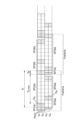
- FIG. 5 shows the timing of the exposure operation and the timing of the signal readout operation for each subframe period obtained by temporally dividing the frame period, for each of the charge readout regions 22 1 to 22 4 corresponding to the control electrodes G 1 to G 4 .
- FIGS. 6A and 6B show timings of electric signals output from the vertical reading control circuit 41 for each row of the pixel circuits 13 and control pulses output from the pixel driver 32 in correspondence with the operation shown in FIG. Timing Chart FIG.
- FIG. 7 is a timing chart for explaining the timing of the control pulses shown in FIG.
- a period that occupies one frame period TF is divided into a plurality of rectangular blocks whose horizontal size corresponds to the length of time.
- An identification indicating the type of processing controlled by the signal readout circuit 15 is attached. Specifically, the period during which the exposure operation is performed is indicated by a white rectangular block, and the period during which the charge reset operation is performed is indicated by a hatched rectangular block with the symbol PRST . The period during which the read operation is performed is indicated by a hatched rectangular block labeled PR .
- subframe periods SF(1) and SF(3) are set for the charge readout regions 22 1 and 22 2 of one of the grouped groups.
- Subframe periods SF(2) and SF(4) parallel to the subframe periods SF(1) and SF(3) are provided for the charge readout regions 22 3 and 22 4 of the other group. is set.
- the pixel driver 32 controls An exposure operation is performed to transfer charges from the photoelectric conversion region 21 to the charge readout regions 22 1 and 22 2 , and then a signal readout operation to read detection signals from the charge readout regions 22 1 and 22 2 under the control of the signal readout circuit 15 . is executed.
- an exposure operation targeting the charge readout regions 22 1 and 22 2 is performed under the control of the pixel driver 32, and then signal readout is performed.
- a signal readout operation targeting the charge readout regions 22 1 and 22 2 is executed. Further, in the sub-frame period SF(2) that starts simultaneously with the sub-frame period SF(1), an exposure operation targeting the charge readout regions 22 3 and 22 4 is performed under the control of the pixel driver 32, and then, A signal readout operation targeting the charge readout regions 22 3 and 22 4 is executed under the control of the signal readout circuit 15 . Further, in the next subframe period SF(4) following the subframe period SF(2), an exposure operation targeting the charge readout regions 22 3 and 22 4 is performed under the control of the pixel driver 32, and then, A signal readout operation targeting the charge readout regions 22 3 and 22 4 is executed under the control of the signal readout circuit 15 .
- the length T R of the period P R of the signal readout operation whose execution is controlled in each of the subframe periods SF(1) to SF(4) is determined by the number of rows of the pixel circuits 13 and the performance of the signal readout function. is set, and the length of the period of the exposure operation whose execution is controlled in each subframe period SF(1) to SF(4) is determined by the first to fourth control pulses G(1) applied in each period. A length corresponding to the delay time of ⁇ G(4) is set.
- Each control pulse G(X) (X is an integer of 1, 2, 3, or 4) shown in FIG.
- the number " k " attached to this symbol Wk corresponds to the delay time of the control pulse G(X) with respect to the pulse light LP .
- the reset signal RT1 output for resetting the charge readout regions 22 1 and 22 2 of one group is sequentially applied to each row. turned on.
- the control pulses G(1) and G(2) for controlling the exposure operation of the charge readout regions 22 1 and 22 2 of one group are applied. , is repeatedly turned on so as to set a constant delay time for each pulsed light LP .
- the control pulse G(1) is set to the timing specified by reference W1
- the control pulse G(2) is set to the timing specified by reference W2 .
- the select signal SL1 output for selecting the charge readout regions 22 1 and 22 2 of one group during signal readout is applied to each row. are sequentially turned on at the same time, the reset signal RT1 for charge reset of the charge readout regions 22 1 and 22 2 is sequentially turned on for each row at the timing after the selection signal SL1 is turned on.
- the control pulse for controlling the exposure operation of the charge readout regions 22 3 and 22 4 of the other group is G(3) and G(4) are repeatedly turned on so as to set a constant delay time for each pulsed light LP .
- the control pulse G(3) is set to the timing specified by reference W3
- the control pulse G(4) is set to the timing specified by reference W4 .
- the select signal SL2 output for selecting the charge readout regions 22 3 and 22 4 of the other group during signal readout is applied to each row. are sequentially turned on at the same time, the reset signal RT2 for charge reset of the charge readout regions 22 3 and 22 4 is sequentially turned on for each row at the timing after the selection signal SL2 is turned on.
- the control pulse G for controlling the exposure operation of the charge readout regions 22 1 and 22 2 of one group is (1) and G(2) are repeatedly turned on so as to set a constant delay time for each pulsed light LP .
- the control pulse G(1) is set to the timing specified by reference W7
- the control pulse G(2) is set to the timing specified by reference W8 .
- the signal readout operation is performed in the same manner as in the subframe period SF(1).
- each of the delay times of G(3) and G(4) is set to the time specified by symbols W5 and W6 .
- the lengths of the exposure operation periods T EX1 to T EX4 in the subframe periods SF(1) to SF(4) are the control pulses G(1) to G
- Different times are set according to the length of the delay time in (4), and the longer the delay time, the longer the subframe period.
- the delay time in subframe period SF(2) is longer than the delay time in subframe period SF(1) by about twice the duration T1 .
- the delay time of subframe period SF(4) is longer than the delay time of subframe period SF(2) by about twice the duration T1
- the delay time of subframe period SF(4) is longer than the delay time of subframe period SF(4).
- the delay time of the subframe period SF(3) is twice as long as the duration T1 .
- the subframe periods SF(1), SF(2), SF(4), and SF(3) are set so that these periods become longer in this order .
- :T EX2 :T EX4 :T EX3 1:4:9:16.
- the light source driver 31 and the pixel driver 32 operate the control pulse G(1 ) to G(4) and the timing of the pulsed light LP are set (light source control step, charge transfer control step). Specifically, in each subframe period SF(1) to SF(4), the delay times of the control pulses G(1) to G(4) for each group of the charge readout regions 22 1 to 22 4 to be controlled are constant. , the delay times of the control pulses G(1) to G(4) to be controlled are set to different times during the subframe periods SF(1) to SF(4), and the subframe periods SF(1) to The length of each SF(4) is set to be longer as the delay time of the control pulses G(1) to G(4) to be controlled is longer.
- the signal readout circuit 15 via the voltage detection means 26 1 to 26 4 of each pixel circuit 13, Detection signals are read out from the charge readout regions 22 1 to 22 4 for each row of the pixel circuit 13, and these detection signals are converted into digital values and output to the arithmetic circuit 17 (signal readout step).
- the signal readout circuit 15 controls the two charge readout regions 22 1 and 22 2 or the two charge readout regions belonging to the group to be controlled at different timings for each of the subframe periods SF(1) to SF(4). Detection signals are read out in parallel from 22 3 and 22 4 .
- the arithmetic circuit 17 calculates distance information for each pixel in units of one frame period (distance calculation step). However, the arithmetic circuit 17 may calculate distance information by averaging calculation results for each of a plurality of frame periods.
- the detection signals S 1 (1) and S 2 ( 1) from the charge readout regions 22 1 and 22 2 obtained by the signal readout operation in the subframe period SF (1) , the subframe period SF Detection signals S 3 (1) and S 4 (1 ) from the charge readout regions 22 3 and 22 4 obtained by the signal readout operation in (2), and obtained by the signal readout operation in the subframe period SF(3) Detection signals S 1 (2) and S 2 (2) from the charge readout regions 22 1 and 22 2 and from the charge readout regions 22 3 and 22 4 obtained by the signal readout operation in the subframe period SF(4) Based on the detection signals S 3 (2) and S 4 (2) , using the following equations (1) to (4), the difference values S 1-3 (1) , S 2-4 (1) , the difference The values S 1-3 (2) and S 2-4 (2) are calculated.
- These calculation formulas also include weighting calculation according to the length of the subframe periods SF(1) to SF(4), that is, the number of application of the control pulses G(1) to G(4).
- S 1-3 (1) 16 x ⁇ (1/1) x S 1 (1) - (1/4)
- S 3 (1) ⁇ ...(1)
- S 2 ⁇ 4 (1) 16 ⁇ (1/1) ⁇ S 2 (1) ⁇ (1/4)S 4 (1) ⁇ ...(2)
- S 1 ⁇ 3 (2) ⁇ 16 ⁇ (1/16) ⁇ S 1 (2) ⁇ (1/9)S 3 (2) ⁇ ...(3)
- S 2 ⁇ 4 (2) ⁇ 16 ⁇ (1/16) ⁇ S 2 (2) ⁇ (1/9)S 4 (2) ⁇ ...(4)
- the arithmetic circuit 17 calculates the distance information using the calculation method disclosed in International Publication WO2019/078366.
- the arithmetic circuit 17 calculates the following formula based on these difference values S 1-3 (1) , S 2-4 (1) , S 1-3 (2) , S 2-4 (2) Using (5) and (6), the values of the distance data validity determination signals S A (1) and S A (2) are calculated.
- S A (1)
- S A (2)
- the detection signals S 1 (1) to S 4 It is determined whether the distance calculation using (1) , S 1 (2) to S 4 (2) is valid.
- the arithmetic circuit 17 calculates the values of the first distance calculation reference signal X R (1) and the second distance calculation reference signal Y R (1) using the following equations (7) and (8). be.
- X R (1) 1-S 1-3 (1) /S A (1) (7)
- Y R (1) 2-S 2-4 (1) /S A (1) (8)
- the arithmetic circuit 17 calculates the distance calculation reference signals X R (B) , Y R (B) , X R (2) and Y R (2) using the following equations (9) to (12). value is calculated.
- the arithmetic circuit 17 converts the distance calculation reference signals XR (1) , XR (B) , XR (2) and the distance calculation reference signals YR (1) , It is selected from Y R (B) and Y R (2) .
- the arithmetic circuit 17 converts the distance calculation reference signals XR (1) , XR (B) , XR (2) and the distance calculation reference signals YR (1) , It is selected from Y R (B) and Y R (2) .
- the distance calculation reference signal S A ( 1) is equal to or greater than the threshold Th 1
- the distance calculation reference signal X Either R (2) or Y R (2) is selected.
- the distance calculation reference signals X R (1) and X R (2) ) and the distance calculation reference signals Y R (1) and Y R (2) are Either of the range calculation reference signals X R (B) and Y R (B) is selected depending on the .
- the arithmetic circuit 17 calculates the selected distance calculation reference signals XR (1) , XR (B) , XR (2) , YR (1) , YR (B) , YR Based on (2) , the distance of the object S is calculated, the calculation result is reflected in the distance information of the corresponding pixel, and a distance image including the distance information of each pixel is generated and output.
- the light source 11 periodically and repeatedly generates the pulsed light LP within the periodic frame period TF , and delays the generation of the pulsed light LP to generate the pulsed light LP within the frame period TF .
- time windows are respectively set for the first to fourth charge readout regions 22 1 to 22 4 , and the first to fourth charge readout regions 22 1 to 22 are read from the photoelectric conversion region 21 of the pixel circuit 13 in the respective time windows. 4 is transferred.
- a detected signal is read out.
- detection signals are read at different timings for each group of the charge readout regions 22 1 to 22 4 divided into two.
- one group of the charge readout regions 22 1 to 22 4 in which a time window corresponding to the timing of the reflected light L R of the pulsed light L P generated at a short distance is set, and the pulsed light L generated at a long distance.
- a detection signal can be read out at different timings from the other group of charge readout regions 22 1 to 22 4 in which a time window corresponding to the timing of the reflected light L R of P is set, and a limited number of frames can be read out.
- the exposure time of the reflected light L 2 R can be changed between the two groups of the charge readout regions 22 1 to 22 4 within the period T F .
- the period of the signal readout operation for one group can be set to the period of the exposure operation for another group, and the period of the exposure operation for each group can be lengthened.
- the period of the signal readout operation for one group can be set to the period of the exposure operation for another group, and the period of the exposure operation for each group can be lengthened.
- the pixel driver 32 performs the sub-frame periods SF(1) to (4) sandwiched between the signal readout processing timings of the two groups of the charge readout regions 22 1 to 22 4 divided into two.
- the control pulses G(1) to G(4) applied corresponding to the groups of the charge readout regions 22 1 to 22 4 are controlled so that the delay time with respect to the generation timing of the pulsed light L P is maintained substantially constant.
- the subframe periods SF(1) to SF(4) in which the delay time with respect to the timing of the pulsed light L P is set substantially constant from the groups of the charge readout regions 22 1 to 22 4 elapse.
- the detection signal is read out later.
- the exposure time can be set according to the distance of the object to be measured, further improving the distance resolution. be able to.
- the signal readout circuit 15 includes a plurality of charge readout regions 22 1 to 22 4 included in the group of the charge readout regions 22 1 to 22 4 divided into two, and electrically connected to each of the charge readout regions 22 1 to 22 4 via switches.
- the detection signals are read out in parallel from the plurality of charge readout regions 22 1 to 22 4 via the plurality of wiring portions L3.
- the detection signals can be read out in parallel from each of the groups of the charge readout regions 22 1 to 22 4 divided into two, and the efficiency of the signal readout operation can be improved.
- the exposure time of the reflected light L R within the limited frame period TF can be ensured, and an image signal with further improved distance resolution can be generated.
- the pixel driver 32 sets the delay times of the control pulses G(1) to G(4) to different times between the groups of the charge readout regions 22 1 to 22 4 divided into two, and the signal readout circuit 15 , the timing of the signal readout operation for each group of the charge readout regions divided into two is set so that the longer the delay time, the longer the length of the subframe periods SF(1) to SF(4).
- the exposure time of one group of the charge readout regions 22 1 to 22 4 in which the time window corresponding to the timing of the reflected light L R of the pulsed light L P generated at a long distance is set is The exposure time of the other group of the charge readout regions 22 1 to 22 4 in which the time window corresponding to the timing of the reflected light L R of the pulsed light L P generated at a short distance is set can be set longer. As a result, it is possible to generate an image signal with further improved distance resolution even when the object S in a wide distance range is the object to be measured.
- the distance image sensor 10 of the above embodiment includes a plurality of pixel circuits 13 arranged in a plurality of rows . Control is performed so that the charge accumulation periods of ⁇ 224 are the same. By adopting such a configuration, two-dimensional distance information can be obtained without distortion.
- the signal readout circuit 15 controls to shift the timing of the signal readout operation for each group of the charge readout regions 22 1 to 22 4 between the rows of the plurality of pixel circuits 13 .
- the signal readout circuit 15 can be shared between rows of a plurality of pixel circuits 13, and the configuration of the distance image sensor 10 can be simplified.
- FIG. 8 shows the timing of the exposure operation and signal readout operation for each subframe period controlled by the range image sensor according to the comparative example.
- This comparative example has a configuration similar to that of the pixel circuit 13 of the above-described embodiment, and divides one frame period TF into two subframe periods SF(1) and SF(2). (1), the signal readout operation timing (corresponding to the hatched rectangular block) is set at the end of SF(2). However, in the comparative example, the control pulses G(1) to G(4) are applied at the timings of the exposure operations (corresponding to the rectangular blocks shown in white) within the subframe periods SF(1) and SF(2).
- T F 2 ⁇ T R +(1+4) ⁇ T A0
- the ratio of the period TA,max of the exposure operation in the subframe period SF(3) in this embodiment is calculated on the premise of the control state shown in FIG.
- T F 2 ⁇ T R +(2+16) ⁇ T A0
- T A,max /T F 16 ⁇ (f M ⁇ 1)/ ⁇ (2+16) ⁇ f M ⁇
- T A,max /T F 0.78
- the pixel circuit 13 is provided with the four charge readout regions 22 1 to 22 4 . (integer of 2 or more) may be provided in the configuration of the charge readout region, which is also referred to as " M1 tap".
- the control electrodes and the voltage detection means are provided corresponding to the number M1 of the charge readout regions, and the pixel driver 32 provides the first to M1th control pulses G ( 1) to G(M 1 ) are generated, the signal readout circuit 15 reads out the 1st to M 1th detection signals from the respective charge readout regions, and the arithmetic circuit 17 causes the signal readout circuit 15 to read the respective charge Distance information is calculated based on the 1st to M1th detection signals read out from the readout area.
- FIG. 9 is a circuit diagram showing a detailed configuration of a modified pixel circuit 13 having a 6-tap configuration.
- the pixel circuit 13 includes first to sixth charge readout regions 22 1 to 22 6 , first to sixth control electrodes G 1 to G 6 , and first to sixth voltage detection means 26 1 to 26 6 are provided.
- the first to sixth charge readout regions 22 1 to 22 6 are divided into two groups: first to third charge readout regions 22 1 to 22 3 and fourth to sixth charge readout regions 22 1 to 22 3 .
- the fourth to sixth charge readout regions 22 4 to 22 6 are connected in parallel to the main wiring portion L3 via the fourth to sixth voltage detection means 26 4 to 26 6 , respectively. It is connected in parallel to the three wiring portions L3.
- the pixel driver 32 of this modified example applies first to sixth control pulses G(1) to G Each delay time of (6) is controlled to be maintained substantially constant.
- the signal readout circuit 15 sets the exposure operation period for each group of the charge readout regions 22 1 to 22 6 within the subframe period in the same manner as in the above-described embodiments, and the charge readout region 22 in the subframe period.
- the timing of the parallel signal read operation is set for each group of 1 to 226 .
- the first to sixth charge readout regions 22 1 to 22 6 may be divided into three groups as shown in FIG.
- the first through sixth charge readout regions 22 1 through 22 6 are in groups of three: first and second charge readout regions 22 1 , 22 2 and third and fourth charge readout regions 22 1 , 22 2 . They are grouped into readout regions 22 3 and 22 4 and fifth and sixth charge readout regions 22 5 and 22 6 .
- the first and second charge readout regions 22 1 and 22 2 are connected in parallel to two wiring portions L 3 via first and second voltage detection means 26 1 and 26 2 , respectively.
- the third and fourth charge readout regions 22 3 and 22 4 are connected in parallel to two wiring portions L 3 via third and fourth voltage detection means 26 3 and 26 4 respectively.
- the fifth and sixth charge readout regions 22 5 and 22 6 are connected in parallel to the two wiring portions L 3 via the fifth and sixth voltage detection means 26 5 and 26 6 , respectively. It is connected.
- FIG. 11 is a circuit diagram showing the detailed configuration of another modified pixel circuit 13 having a 3-tap configuration.
- the pixel circuit 13 includes first to third charge readout regions 22 1 to 22 3 , first to third control electrodes G 1 to G 3 , and first to third voltage detection means 26 1 to 26 3 are provided.
- the first to third charge readout regions 22 1 to 22 3 are grouped into three groups: a first charge readout region 22 1 , a second charge readout region 22 2 and a third charge readout region. 22 3 , and the first to third charge readout regions 22 1 to 22 3 are connected to one line via first to third voltage detection means 26 1 to 26 3 , respectively. It is connected to the wiring part L3.
- the pixel driver 32 of this modified example applies first to third control pulses G(1) to G Each delay time of (3) is controlled to be maintained substantially constant. Further, the signal readout circuit 15 sets the period of the exposure operation for each group of the charge readout regions 22 1 to 22 3 within the subframe period in the same manner as in the above-described embodiments, and the charge readout region 22 in the subframe period. The timing of the signal readout operation is set for each group of 1 to 223 .
- the distance image sensor 10 may be controlled to switch the control timing between groups of charge readout regions in two consecutive one-frame periods.
- FIG. 12 shows the timing of the exposure operation and signal readout operation for each subframe period controlled by the range image sensor according to the modification.
- the pixel driver 32 and the signal readout circuit 15 operate the charge readout regions within the subframe periods SF(1a) to SF(4a) in one frame period Frame1a in the same manner as in the above-described embodiment.
- the timings of the exposure operation and the signal readout operation are set for one group including the charge readout regions 22 1 and 22 2 and the other group including the charge readout regions 22 3 and 22 4 .
- the pixel driver 32 and the signal readout circuit 15 of this modification set each timing within the sub-frame periods SF(1b) to SF(4b) in one frame period Frame1b immediately following one frame period Frame1a.
- the objects are switched between one group containing the charge readout regions 22 1 and 22 2 and the other group containing the charge readout regions 22 3 and 22 4 . That is, the pixel driver 32 sets the delay times of the control pulses G(1) and G( 2 ) for one group including the charge readout regions 22 1 and 22 2 , The setting of the delay times of the control pulses G(3) and G(4) set for the other group including 4 is exchanged. Further, the signal readout circuit 15 sets the timing of the signal readout operation for one group including the charge readout regions 22 1 and 22 2 and sets the timing for the other group including the charge readout regions 22 3 and 22 4 . and the setting of the timing of the signal readout operation.
- the pixel driver 32 and the signal readout circuit 15 set the first sub-frame period SF(1b) of the frame period Frame1b to a timing that overlaps with the last sub-frame period SF(3a) of the frame period Frame1a. This makes it possible to more efficiently secure the period of the exposure operation.
- the arithmetic circuit 17 based on the detection signals S 1 (1) to S 4 (1) and S 1 (2) to S 4 (2) acquired by the signal readout operation in one frame period Frame1a, the above Difference values S 1-3 (1) (Frame1a), S 2-4 (1) (Frame1a), S 1-3 (2) (Frame1a), S 2-4 (2) ( Calculate Frame1a). Furthermore, the arithmetic circuit 17 calculates the following based on the detection signals S 1 (1) to S 4 (1) and S 1 (2) to S 4 (2) acquired by the signal readout operation in one frame period Frame1b immediately after that.
- S 1-3 (1) ⁇ S 1-3 (1) (Frame1a) + S 1-3 (1) (Frame1b) ⁇ /2 (17)
- S 2-4 (1) ⁇ S 2-4 (1) (Frame1a) + S 2-4 (1) (Frame1b) ⁇ /2 (18)
- S 1-3 (2) ⁇ S 1-3 (2) (Frame1a) + S 1-3 (2) (Frame1b) ⁇ /2 (19)
- S 2-4 (2) ⁇ S 2-4 (2) (Frame1a) + S 2-4 (2) (Frame1b) ⁇ /2 (20)
- the arithmetic circuit 17 calculates the distance based on the moving average of the four difference values for each frame period in the same manner as in the above embodiment, and generates a distance image including distance information reflecting the distance. do.
- this modified example it is also possible to generate an image signal with improved distance resolution even when an object S in a wide range of distances is to be measured.
- the distance is calculated by moving average between frame periods, it is possible to cancel or reduce the influence of nonlinear gain variations among the plurality of pixel circuits 13 that output detection signals. can be done.
- the pixel driver 32 and the signal readout circuit 15 set the subframe period for each group of charge readout regions of the pixel circuit 13 .
- the pixel driver 32 and the signal readout circuit 15 according to the modification may divide the N rows of pixel circuits 13 into groups in units of rows, and further allocate a different subframe period to each divided row group.
- FIG. 13 is a diagram showing the timing of the exposure operation and the timing of the signal readout operation for each sub-frame period obtained by temporally dividing the frame period in this modification.
- the pixel driver 32 and the signal readout circuit 15 have different sub-groups for the groups of the charge readout regions for each of the group Gr1 of the pixel circuits 13 in the odd rows and the group Gr2 of the pixel circuits 13 in the even rows.
- a frame period is allocated, and a signal read operation period TR with different timing is set at the end of the subframe period for each of the groups Gr1 and Gr2.
- the subframe periods SF(1), SF(3), and SF(5) are set for the charge readout regions 22 1 to 22 3 of the pixel circuits 13 belonging to the group Gr1.
- subframe periods SF(2) and SF( 4) and SF(6) are set.
- a subframe period SF(26) is set for the charge readout regions 22 1 to 22 3 of the pixel circuits 13 belonging to the group Gr2, and in parallel with the subframe period SF(26), the charge reading regions 22 1 to 22 3 belonging to the group Gr2
- a subframe period SF (25) is set for the charge readout regions 22 4 to 22 6 of the pixel circuit 13 . According to such an example, it is possible to set, for example, a total of 32 sub-frame periods for even-numbered rows and odd-numbered rows within one frame period.
- the continuous control pulses G(1) to G(6), G(D) applied from the pixel driver 32 to the pixel circuits 13 of each row are divided into row groups Gr1, A selection circuit is provided to select and apply to the control electrodes G 1 to G 6 and GD at desired timing within the subframe period of every Gr2. Further, the pixel driver 32 and the signal readout circuit 15 may operate such that the setting of the subframe period for each of the row groups Gr1 and Gr2 as shown in FIG. 13 is switched between two consecutive frame periods.
- the exposure time can be changed more efficiently within a limited frame period. As a result, it becomes easy to generate an image signal with improved distance resolution.
- the pixel driver 32 performs so-called global exposure so that the charge accumulation periods of the first to fourth charge readout regions 22 1 to 22 4 match between the rows of the plurality of pixel circuits 13. I had control to do it.
- the pixel driver 32 performs so-called rolling exposure such that the accumulation periods of the first to fourth charge readout regions 22 1 to 22 4 are sequentially shifted by a constant time between rows of the plurality of pixel circuits 13. can be controlled as follows.
- FIG. 14 shows the timing of the exposure operation period in each row of the pixel circuits 13 when the control by the pixel driver 32 shown in FIGS. 5 and 6 is set to perform rolling exposure. In FIG.
- the horizontal direction corresponds to the passage of time, and the timings of the exposure periods of the respective rows of the pixel circuits are shown arranged in the vertical direction.
- the period TEX1 of the exposure operation in the subframe period SF(1) is controlled so as to be sequentially shifted by a constant period between the pixel circuits 13 of the first to fourth consecutive rows.
- the exposure operation periods T EX2 and T EX3 in the sub-frame periods SF(2) and SF(3) are also sequentially shifted by a constant period between the pixel circuits 13 of the first to fourth rows.
- the waiting time from the exposure operation to the signal readout operation in each row of the plurality of pixel circuits 13 can be shortened, and the dark current (noise) caused by leaked light in the readout detection signal can be reduced. , and it is possible to prevent the influence of the parasitic sensitivity from changing for each row of the pixel circuits 13 . As a result, a two-dimensional image signal with little noise can be obtained.
- FIG. 15 shows an excerpt from the circuit configuration around some pixel circuits 13 in a specific row in the distance image sensor 10 .
- the pixel circuit 13 has the 6-tap configuration shown in FIG.
- Switch circuits 61, 63, and 65 are provided in common for two adjacent pixel circuits 13 in the same row.
- the switch circuit 61 includes six switch elements 67 1 , 69 1 , 67 3 , 69 3 , 67 5 and 69 5 .
- the switch elements 67 1 , 69 1 , 67 3 , 69 3 , 67 5 and 69 5 are, for example, MOS transistors.
- the switch element 671 is connected between the pixel driver 32 and the control electrodes G1 of the two pixel circuits 13 in each row, its source is connected to the pixel driver 32 via the wiring portion L1, and its drain is connected to the pixel driver 32 via the wiring portion L1. It is connected to the control electrodes G1 of the two pixel circuits 13, and its gate is connected to the pixel driver 32 via the wiring portion L4 provided for each row.
- the switch element 691 is connected between the control electrode G1 of the two pixel circuits 13 and a fixed potential (ground potential in this embodiment), and its drain is connected to the control electrode G1 of the two pixel circuits 13 .
- the source is connected to a fixed potential, and the gate is connected to the pixel driver 32 via a wiring portion L4 provided for each row.
- Selection signals S R and U R that change complementarily are supplied from the pixel driver 32 to the gates of the switch element 67-1 and the gate of the switch element 69-1 , respectively, so that the signal from the pixel driver 32 passes through the wiring portion L1.
- Either the control pulse DG 1 for the control electrode G 1 supplied as a control pulse DG 1 or a fixed potential is selectively applied to the control electrodes G 1 of the two pixel circuits 13 .
- the switch elements 67 3 , 69 3 , 67 5 and 69 5 also have similar configurations. That is, the switch element 673 is connected between the pixel driver 32 and the control electrodes G3 of the two pixel circuits 13 in each row, and the switch element 693 is connected between the control electrodes G3 of the two pixel circuits 13 in each row. connected between a fixed potential.
- the switch element 67_3 and the switch element 69_3 operate based on the selection signals S R and U R supplied from the pixel driver 32 to control the control pulse DG 3 for the control electrode G 3 supplied from the pixel driver 32 or the fixed potential. to the control electrodes G3 of the two pixel circuits 13 selectively.
- the switch element 675 is connected between the pixel driver 32 and the control electrodes G5 of two pixel circuits 13 in each row, and the switch element 695 is connected between the control electrodes G5 of the two pixel circuits 13 and a fixed potential. is connected between The switch element 67_5 and the switch element 69_5 operate based on the selection signals S R and U R supplied from the pixel driver 32 to generate a control pulse DG 5 for the control electrode G 5 supplied from the pixel driver 32 or a fixed potential. is selectively applied to the control electrodes G5 of the two pixel circuits 13.
- Switch circuit 63 includes six switch elements 67 2 , 69 2 , 67 4 , 69 4 , 67 6 , and 69 6 having the same configuration as switch circuit 61 .
- the switch element 67_2 and the switch element 69_2 selectively switch either the control pulse DG2 for the control electrode G2 or the fixed potential based on the selection signals S R and U R supplied from the pixel driver 32 . is applied to the control electrode G2 of one pixel circuit 13;
- the switch element 67 4 and the switch element 69 4 selectively switch either the control pulse DG 4 for the control electrode G 4 or the fixed potential based on the selection signals S R and U R supplied from the pixel driver 32 .
- the switch element 676 and the switch element 696 selectively switch either the control pulse DG6 for the control electrode G6 or the fixed potential based on the selection signals S R and U R supplied from the pixel driver 32 . is applied to the control electrode G6 of one pixel circuit 13;
- the switch circuit 65 includes two switch elements 67 D and 69 D configured similarly to the switch circuit 61 .
- the switch element 67 D and the switch element 69 D operate based on the selection signals S R and U R supplied from the pixel driver 32 to generate a control pulse DGD for the control electrode G D or a fixed potential (positive potential in this embodiment). is selectively applied to the control electrodes GD of the two pixel circuits 13 .
- FIG. 16 and 17 are timing charts showing the control timing of the exposure operation in the modified example, and FIG. FIG. 17 shows the control timing at the first generation timing of the light LP , and FIG. 17 shows the control timing at the first generation timing of the pulsed light LP immediately after the subframe period SF(6) shown in FIG. .
- U R (e) shows timings of control pulses G(1)(e) to G(6)(e) and G(D)(e) applied to the pixel circuits 13 of odd rows.
- the light supplied from the pixel driver 32 is common between the rows.
- the control pulses DG 1 to DG 3 are turned on at any timing specified by symbols W 1 to W 3 and at any timing specified by symbols W 76 to W 78 , and turned off at other timings.
- the control pulse DG D supplied from the pixel driver 32 and common between the rows has timings including timings specified by symbols W 1 to W 3 and timings including timings specified by symbols W 76 to W 78 . It is set to turn off and turn on during other periods.
- the selection signal S R (o) set in the odd rows is turned on across the timings specified by the symbols W 1 to W 3
- the selection signal S R (o) set in the even rows is turned on.
- (e) is turned on across the timings specified by symbols W 76 to W 78 .
- the control pulses G(1)(o) to G(3)(o) applied to the odd-numbered pixel circuits 13 are turned on at the timings specified by the symbols W1 to W3 .
- the control pulse G(D)(o) applied to the odd-numbered pixel circuits 13 is set to turn off at timings including timings specified by symbols W 1 to W 3 .
- control pulses G(1)(e) to G(3)(e) applied to the pixel circuits 13 of the even rows are set to turn on at the timings specified by the symbols W76 to W78 .
- control pulse G(D)(e) applied to the pixel circuits 13 in the even rows is set to turn off at timings including timings specified by symbols W76 to W78 .
- the control pulses DG 1 to DG 6 common between the rows supplied from the pixel driver 32 are , are set to turn on at any timing specified by symbols W 22 to W 27 and at any timing specified by symbols W 73 to W 78 , and to turn off at other timings.
- the control pulse DG D common between the rows supplied from the pixel driver 32 has timings including timings specified by symbols W 22 to W 27 and timings including timings specified by symbols W 73 to W 78 . It is set to turn off and turn on during other periods.
- the selection signal S R (o) set for odd rows is turned on across the timings specified by symbols W 22 to W 27
- the selection signal S R (o) set for even rows is turned on.
- (e) is turned on across the timings specified by symbols W 73 to W 78 .
- the control pulses G(1)(o) to G(6)(o) applied to the odd-numbered pixel circuits 13 are turned on at the timings specified by the symbols W22 to W27 .
- the control pulse G(D)(o) applied to the odd-numbered pixel circuits 13 is set to turn off at timings including timings specified by symbols W 22 to W 27 .
- control pulses G(1)(e) to G(6)(e) applied to the pixel circuits 13 of the even-numbered rows have timings specified by symbols W 76 to W 78 and W 73 to W 75 respectively.
- control pulse G(D)(e) applied to the even-numbered pixel circuits 13 is set to turn off at timings including the timings specified by symbols W73 to W78 . be.
- control pulses DG 1 to DG 6 and DG D from the pixel driver 32 can be selectively applied to each row of the plurality of pixel circuits 13 .
- the charge accumulation period of the charge readout region can be controlled for each row of the plurality of pixel circuits 13, and image signals with improved distance resolution can be easily generated.
- the charge transfer control means applies the charge corresponding to the group of the charge readout regions within the subframe period sandwiched between the readout timings of the groups of the charge readout regions divided into N. It is preferable to maintain a substantially constant delay time with respect to the generation timing of the control pulse. With such a configuration, the detection signal is read out from each charge readout region group after the passage of the subframe period in which the delay time with respect to the timing of the pulsed light is set substantially constant. As a result, by changing the exposure time of the reflected light between groups of charge readout regions, the exposure time can be set according to the distance of the object to be measured, and the distance resolution can be further improved.
- the signal readout means includes a plurality of signal lines electrically connected to each of the plurality of charge readout regions included in the group of the N-divided charge readout regions via switches, and the switch is turned on at the readout timing. It is also preferable to read detection signals in parallel from a plurality of charge readout regions through a plurality of signal lines. In this case, detection signals can be read out in parallel from each of the N-divided groups of charge readout regions, and the efficiency of the readout process can be improved. As a result, it is possible to ensure the exposure time of the reflected light within the limited frame period, and to generate an image signal with further improved distance resolution.
- the charge transfer control means sets the delay time of the control pulse to be different between the groups of the N divided charge readout regions
- the signal readout means sets the read timing for each group of the N divided charge readout regions. is also preferably set such that the larger the delay, the larger the subframe period.
- the exposure time of the group of charge readout regions for which the time window corresponding to the timing of the reflected light of the pulsed light generated at a long distance is set is adjusted to that of the reflected light of the pulsed light generated at a short distance.
- the time window corresponding to the timing can be greater than the exposure time of the group of charge readout regions set.
- the charge transfer control means includes, in one frame period, a delay time with respect to the generation timing of a control pulse applied corresponding to one group of charge readout regions, and a control pulse applied corresponding to another group of charge readout regions. It is also preferable to set the delay time with respect to the generation timing of the control pulse to be switched in the frame period immediately after one frame period. In this case, the deviation between the exposure time of one group of charge readout regions and the exposure time of another group of charge readout regions in consecutive frame periods can be reduced. As a result, it is possible to ensure the exposure time of the reflected light within the limited frame period, and to generate an image signal with further improved distance resolution.
- the signal readout means exchanges readout timing for one group of charge readout regions and readout timing for another group of charge readout regions in one frame period in a frame period immediately after one frame period. It is also preferable to set In this way, the bias between the exposure time of one group of charge readout regions and the exposure time of the other charge readout region groups in consecutive frame periods is reduced, and detection signals are read out from these groups. be able to. As a result, it is possible to obtain a detection signal in which the exposure time of the reflected light is ensured within the limited frame period, and to generate an image signal with further improved distance resolution.
- a plurality of pixel circuit portions arranged in a plurality of rows are provided, and the signal readout means controls the charge accumulation periods of the first to Mth charge readout regions to match between the rows of the plurality of pixel circuit portions. , is also preferred. By adopting such a configuration, two-dimensional distance information can be obtained without distortion.
- a plurality of pixel circuit sections arranged in a plurality of rows are provided, and the signal readout means controls to shift the charge accumulation periods of the first to Mth charge readout regions between the rows of the plurality of pixel circuit sections. is also preferred. By adopting such a configuration, it is possible to shorten the waiting time from exposure to readout in the rows of the plurality of pixel circuit units, and to reduce noise in the readout detection signal. As a result, a two-dimensional image signal with little noise can be obtained.
- switch elements are provided which are respectively connected between the charge transfer control means and the control electrodes of the plurality of pixel circuit portions in every plurality of rows and between the control electrodes and a fixed potential. It is also preferable to selectively apply either the control pulse or the fixed potential to the control electrode in response to the selection signal. By doing so, it is possible to selectively apply the control pulse from the charge transfer control means to each row of the plurality of pixel circuit portions. As a result, the charge accumulation period of the charge readout region can be controlled for each row of a plurality of pixel circuit portions, and image signals with improved distance resolution can be easily generated.
- Reference numerals 10 distance image sensor, LP : pulsed light, LR : incident pulsed light, S: object, 22 1 to 22 6 : charge readout region, G 1 to G 6 : control electrode, 26 1 to 26 6 : voltage Detector 11 Light source 13 Pixel circuit (pixel circuit section) 21 Photoelectric conversion region 31 Light source driver 32 Pixel driver (charge transfer control means) 15 Signal readout circuit (signal readout means) 17... Arithmetic circuit, 53... Selection transistor (switch), 67 1 to 67 6 , 67 D , 69 1 to 69 6 , 69 D ... Switch element, L3... Wiring part (signal line).
Abstract
A distance image sensor 10 comprises a light source 11 for generating pulsed light LP, a light source driver 31 for controlling the light source 11, a pixel circuit 13 including a photoelectric conversion region 21, electric charge readout regions 221 to 224 and control electrodes G1 to G4, a pixel driver 32 for delaying a generation timing of the pulsed light LP and repeatedly applying control pulses G(1) to G(4) to the control electrodes G1 to G4 in a frame period, and a signal readout circuit 15 for reading out a detection signal of an amount of charge accumulated in the electric charge readout regions 221 to 224, wherein the signal readout circuit 15 reads out the detection signal from groups of the electric charge readout regions 221 to 224, divided into N (N is an integer at least equal to 2) groups, from among the electric charge readout regions 221 to 224, with a different readout timing for each group of the electric charge readout regions 221 to 224, divided into said N groups, in the frame period.
Description
本開示は、画素毎に距離情報を含む距離画像を生成する距離画像測定装置及び距離画像測定方法に関する。
The present disclosure relates to a distance image measurement device and a distance image measurement method that generate a distance image including distance information for each pixel.
従来から、光の飛行時間を用いて距離情報を含む画像信号を生成する装置が用いられている(例えば、下記特許文献1参照)。この下記特許文献1に記載の装置は、光源からパルス光を発生させ、それに応じて発生した電荷を、制御パルスによって設定される異なる期間で画素回路内の複数の電荷読出領域に蓄積し、複数の電荷読出領域のそれぞれの電圧を検出信号として読み出し、それらの検出信号を基に画素ごとの距離を計算することにより距離情報を取得する。
Conventionally, there has been used a device that generates an image signal containing distance information using the time of flight of light (see, for example, Patent Document 1 below). The device described in Patent Document 1 below generates pulsed light from a light source, accumulates charges generated accordingly in a plurality of charge readout regions in a pixel circuit for different periods set by control pulses, and stores a plurality of charge readout regions. are read out as detection signals, and the distance information is obtained by calculating the distance for each pixel based on the detection signals.
上述した従来の装置においては、広い距離範囲にある対象物を測定対象とする際に距離分解能を向上させることが望まれていた。
In the above-described conventional devices, it was desired to improve the distance resolution when measuring objects in a wide range of distances.
本開示は、上記課題に鑑みて為されたものであり、広い距離範囲にある対象物を測定対象とする場合に距離分解能を向上された画像信号を生成することが可能な距離画像測定装置及び距離画像測定方法を提供することを目的とする。
The present disclosure has been made in view of the above problems, and provides a distance image measuring apparatus capable of generating an image signal with improved distance resolution when measuring an object in a wide distance range, and An object of the present invention is to provide a distance image measurement method.
上記課題を解決するため、本開示の一形態にかかる距離画像測定装置は、パルス光を発生させる光源と、パルス光を、周期的なフレーム期間内で繰り返し発生させるように光源を制御する光源制御手段と、光を電荷に変換する光電変換領域、光電変換領域に近接して互いに離間して設けられた第1~第M(Mは2以上の整数)の電荷読出領域、及び光電変換領域と第1~第Mの電荷読出領域とに対応してそれぞれ設けられ、光電変換領域と第1~第Mの電荷読出領域との間における電荷転送のための第1~第Mの制御パルスを印加するための第1~第Mの制御電極を有する画素回路部と、光源制御手段によるパルス光の発生タイミングに遅延させて、フレーム期間内に第1~第Mの制御電極に第1~第Mの制御パルスを繰り返し印加する電荷転送制御手段と、画素回路部の第1~第Mの電荷読出領域に蓄積された電荷の量である第1~第Mの電荷量に応じた検出信号を、第1~第Mの電荷読出領域から読み出す信号読出手段と、を備え、信号読出手段は、第1~第Mの電荷読出領域のうちからN(Nは2以上の整数)分割された電荷読出領域のグループから、フレーム期間内におけるN分割された電荷読出領域のグループ毎の異なる読み出しタイミングで、検出信号を読み出す。
In order to solve the above problems, a distance image measuring device according to an embodiment of the present disclosure includes a light source that generates pulsed light, and light source control that controls the light source to repeatedly generate the pulsed light within a periodic frame period. means, a photoelectric conversion region that converts light into electric charge, first to Mth charge readout regions (M is an integer equal to or greater than 2) provided adjacent to the photoelectric conversion region and separated from each other, and a photoelectric conversion region 1st to Mth control pulses are applied for charge transfer between the photoelectric conversion region and the first to Mth charge readout regions, respectively provided corresponding to the first to Mth charge readout regions. and a pixel circuit portion having first to Mth control electrodes for controlling the pulsed light, and delaying the generation timing of the pulsed light by the light source control means so that the first to Mth control electrodes are applied to the first to Mth control electrodes within the frame period. a charge transfer control means for repeatedly applying a control pulse of , and a detection signal corresponding to the first to Mth charge amounts, which are the amounts of charges accumulated in the first to Mth charge readout regions of the pixel circuit section, signal readout means for reading out from the first to Mth charge readout regions, wherein the signal readout means reads out charges divided by N (N is an integer equal to or greater than 2) from the first to Mth charge readout regions. A detection signal is read from a group of regions at different read timings for each group of N-divided charge readout regions within a frame period.
あるいは、本開示の他の形態にかかる距離画像測定方法は、光源制御手段が、パルス光を周期的なフレーム期間内で繰り返し発生させるように光源を制御する光源制御ステップと、光を電荷に変換する光電変換領域、光電変換領域に近接して互いに離間して設けられた第1~第M(Mは2以上の整数)の電荷読出領域、及び光電変換領域と第1~第Mの電荷読出領域とに対応してそれぞれ設けられ、光電変換領域と第1~第Mの電荷読出領域との間における電荷転送のための第1~第Mの制御パルスを印加するための第1~第Mの制御電極を有する画素回路部を用いて、電荷転送制御手段が、光源制御手段によるパルス光の発生に遅延させて、フレーム期間内に第1~第Mの制御電極に第1~第Mの制御パルスを繰り返し印加する電荷転送制御ステップと、信号読出手段が、画素回路部の第1~第Mの電荷読出領域に蓄積された電荷の量である第1~第Mの電荷量に応じた検出信号を、第1~第Mの電荷読出領域から読み出す信号読出ステップと、を備え、信号読出ステップでは、第1~第Mの電荷読出領域のうちからN(Nは2以上の整数)分割された電荷読出領域のグループから、フレーム期間内におけるN分割された電荷読出領域のグループ毎の異なる読み出しタイミングで、検出信号を読み出す。
Alternatively, a distance image measurement method according to another aspect of the present disclosure includes a light source control step in which the light source control means controls the light source to repeatedly generate pulsed light within a periodic frame period; 1st to Mth charge readout regions (M is an integer equal to or greater than 2) provided close to the photoelectric conversion region and separated from each other, and the photoelectric conversion region and the 1st to Mth charge readout regions 1st to Mth control pulses for charge transfer between the photoelectric conversion region and the first to Mth charge readout regions. , the charge transfer control means delays the generation of pulsed light by the light source control means, and the 1st to Mth control electrodes are applied to the 1st to Mth control electrodes within the frame period. a charge transfer control step of repeatedly applying a control pulse; a signal readout step of reading the detection signal from the first to Mth charge readout regions, and in the signal readout step, the first to Mth charge readout regions are divided by N (N is an integer equal to or greater than 2). A detection signal is read out from the divided charge readout region groups at different readout timings for each group of N divided charge readout regions within the frame period.
上記形態の距離画像測定装置あるいは距離画像測定方法によれば、周期的なフレーム期間内で光源から定期的に繰り返しパルス光が発生し、パルス光の発生に遅延させてフレーム期間内で第1~第Mの電荷読出領域に対する時間ウィンドウがそれぞれ設定され、それぞれの時間ウィンドウで画素回路部の光電変換領域から第1~第Mの電荷読出領域に電荷が転送される。さらに、画素回路部の第1~第Mの電荷読出領域から第1~第Mの電荷量に応じた検出信号が読み出される。このとき、N分割された電荷読出領域のグループ毎に異なるタイミングで検出信号が読み出される。これにより、近距離で生じたパルス光の反射光のタイミングに対応する時間ウィンドウが設定された電荷読出領域のグループと、遠距離で生じたパルス光の反射光のタイミングに対応する時間ウィンドウが設定された電荷読出領域のグループとの間で、別々のタイミングで検出信号を読み出すことができ、限られたフレーム期間の時間内での電荷読出領域のグループ間で反射光の露光時間を変化させることができる。その結果、広い距離範囲にある対象物を測定対象とする場合にも距離分解能が向上された画像信号を生成することができる。
According to the range image measuring device or the range image measuring method of the above configuration, the pulsed light is periodically and repeatedly generated from the light source within the periodic frame period, and the generation of the pulsed light is delayed to produce the first to the first to the next within the frame period. A time window is set for each of the Mth charge readout regions, and charges are transferred from the photoelectric conversion region of the pixel circuit section to the first to Mth charge readout regions in each time window. Furthermore, detection signals corresponding to the first to Mth charge amounts are read out from the first to Mth charge readout regions of the pixel circuit section. At this time, detection signals are read at different timings for each group of the N-divided charge readout regions. As a result, a group of charge readout regions in which a time window corresponding to the timing of the reflected light of the pulsed light generated at a short distance is set and a time window corresponding to the timing of the reflected light of the pulsed light generated at a long distance are set. A detection signal can be read out at different timings from a group of charge readout regions arranged as above, and the exposure time of reflected light can be changed between the groups of charge readout regions within a limited frame period. can be done. As a result, it is possible to generate an image signal with improved distance resolution even when an object in a wide range of distances is to be measured.
本開示によれば、広い距離範囲にある対象物を測定対象とする際に距離分解能を向上させることができる。
According to the present disclosure, it is possible to improve the distance resolution when measuring an object in a wide range of distances.
以下、図面を参照しつつ本開示に係る距離画像測定装置の好適な実施形態について詳細に説明する。なお、図面の説明においては、同一又は相当部分には同一符号を付し、重複する説明を省略する。
A preferred embodiment of the distance image measuring device according to the present disclosure will be described in detail below with reference to the drawings. In the description of the drawings, the same or corresponding parts are denoted by the same reference numerals, and overlapping descriptions are omitted.
まず、図1を参照して、本開示の距離画像測定装置の好適な一実施形態に係る距離画像センサ10の機能および構成を説明する。図1に示す距離画像センサ10は、飛行時間法を利用して画素毎に距離情報を含む距離画像を生成する装置であり、光源11と、複数の画素回路(画素回路部)13と、信号読出回路(信号読出手段)15と、演算回路17と、光源ドライバ(光源制御手段)31と、画素ドライバ(電荷転送制御手段)32とを備える。
First, with reference to FIG. 1, the function and configuration of a range image sensor 10 according to a preferred embodiment of the range image measurement device of the present disclosure will be described. A distance image sensor 10 shown in FIG. 1 is a device that generates a distance image including distance information for each pixel using the time-of-flight method. It includes a readout circuit (signal readout means) 15 , an arithmetic circuit 17 , a light source driver (light source control means) 31 , and a pixel driver (charge transfer control means) 32 .
光源11は、飛行時間(TOF:Time Of Flight)方式による距離計測を行うために、対象物Sに照射するパルス光LPを発生させる装置である。光源11は、例えば、発光ダイオードあるいはレーザダイオード等の半導体発光素子とその半導体発光素子を駆動する駆動回路とによって構成される。光源11としては、近赤外領域、可視光領域等の波長領域の光を発生させる素子を用いることができる。
The light source 11 is a device that generates a pulsed light LP to irradiate the object S in order to perform distance measurement by the time of flight (TOF) method. The light source 11 is composed of, for example, a semiconductor light emitting element such as a light emitting diode or a laser diode and a driving circuit for driving the semiconductor light emitting element. As the light source 11, an element that generates light in a wavelength range such as a near-infrared range and a visible light range can be used.
さらに、距離画像センサ10は複数の画素回路13を備える。複数の画素回路13は、2次元方向(例えば、列方向および行方向)に2次元アレイ状に配列されてイメージセンサを構成し、対象物Sによってパルス光LPが反射されて生じた入射パルス光LRを光電変換することにより検出信号を生成する。
Further, the range image sensor 10 comprises a plurality of pixel circuits 13. FIG. A plurality of pixel circuits 13 are arranged in a two-dimensional array in two-dimensional directions (for example, column direction and row direction) to form an image sensor . A detection signal is generated by photoelectrically converting the light LR .
加えて、距離画像センサ10は、信号読出回路15、演算回路17、光源ドライバ31、及び画素ドライバ32を備えている。演算回路17は、複数の画素回路13によって生成された検出信号を用いて、対象物Sに関する距離情報を画素ごとに演算し、画素ごとの距離情報が反映された2次元画像情報を含む距離画像を生成及び出力する。信号読出回路15は、複数の画素回路13からの検出信号の読み出しを制御する。光源ドライバ31は、光源11におけるパルス光LPの照射タイミングを制御する。画素ドライバ32は、複数の画素回路13における光電変換領域から電荷読出領域への電荷転送のタイミングを制御する(詳細は後述する。)。演算回路17、光源ドライバ31、及び画素ドライバ32は、CPU,RAM、ROM、および入出力装置等を含むワンチップマイクロコンピュータ等の専用の集積回路によって構成されてもよいし、パーソナルコンピュータ等の汎用コンピュータによって構成されてもよい。本実施形態では、信号読出回路15、演算回路17、光源ドライバ31、及び画素ドライバ32は、画素回路13とともに同一の半導体チップ上に搭載されたオンチップの集積回路によって構成されている。なお、「同一の半導体チップ上」とは、SOI(Silicon On Insulator)技術やTSV(Through Silicon Via)技術を用いて積層された複数の半導体層のうちの異なる半導体上も含まれる。
In addition, the distance image sensor 10 includes a signal readout circuit 15 , an arithmetic circuit 17 , a light source driver 31 and a pixel driver 32 . The arithmetic circuit 17 uses the detection signals generated by the plurality of pixel circuits 13 to calculate distance information about the object S for each pixel, and produces a distance image including two-dimensional image information in which the distance information for each pixel is reflected. is generated and output. The signal readout circuit 15 controls readout of detection signals from the plurality of pixel circuits 13 . The light source driver 31 controls the irradiation timing of the pulsed light LP in the light source 11 . The pixel driver 32 controls the timing of charge transfer from the photoelectric conversion region to the charge readout region in the plurality of pixel circuits 13 (details will be described later). The arithmetic circuit 17, the light source driver 31, and the pixel driver 32 may be configured by a dedicated integrated circuit such as a one-chip microcomputer including CPU, RAM, ROM, input/output devices, etc., or a general-purpose integrated circuit such as a personal computer. It may be configured by a computer. In this embodiment, the signal readout circuit 15, the arithmetic circuit 17, the light source driver 31, and the pixel driver 32 are composed of on-chip integrated circuits mounted on the same semiconductor chip together with the pixel circuit 13. FIG. Note that "on the same semiconductor chip" includes on different semiconductors among a plurality of semiconductor layers stacked using SOI (Silicon On Insulator) technology or TSV (Through Silicon Via) technology.
以下、画素回路13、信号読出回路15、演算回路17、光源ドライバ31、及び画素ドライバ32の構成について詳細に説明する。
The configurations of the pixel circuit 13, the signal readout circuit 15, the arithmetic circuit 17, the light source driver 31, and the pixel driver 32 will be described in detail below.
まず、画素回路13の構成について説明する。画素回路13は、半導体素子によって構成され、入射パルス光LRを電荷に変換する機能を有する光電変換領域21と、光電変換領域21に近接し、かつ互いに離間して設けられた第1~第4の電荷読出領域221~224及び電荷排出領域23と、第1~第4の電荷読出領域221~224及び電荷排出領域23のそれぞれに対応して設けられ、光電変換領域21からそれぞれの領域との間における電荷転送のための制御パルスを印加するための第1~第4の制御電極G1~G4および第5の制御電極GDと、第1~第4の電荷読出領域221~224のそれぞれから検出信号を読み出すための電圧検出手段261~264とを含んでいる。電圧検出手段261~264は、例えば、ソースフォロワアンプを含む増幅器であり、信号読出回路15からの制御によって、選択的にそれぞれの電荷読出領域221~224の基準電位を基準にした電圧を出力する。選択された電圧は、信号読出回路15によって検出および増幅され、増幅されたそれぞれの電荷読出領域221~224の電圧が第1~第4の検出信号として演算回路17に出力される。
First, the configuration of the pixel circuit 13 will be described. The pixel circuit 13 is composed of a semiconductor element, and includes a photoelectric conversion region 21 having a function of converting incident pulsed light L to electric charges, and first to first photoelectric conversion regions 21 provided close to the photoelectric conversion region 21 and spaced apart from each other. 4 charge readout regions 22 1 to 22 4 and charge discharge region 23, and the first to fourth charge readout regions 22 1 to 22 4 and charge discharge region 23, respectively. first to fourth control electrodes G 1 to G 4 and a fifth control electrode G D for applying control pulses for charge transfer between the respective regions, and first to fourth charge readout and voltage detection means 26 1 to 26 4 for reading detection signals from the regions 22 1 to 22 4 respectively. The voltage detection means 26 1 to 26 4 are, for example, amplifiers including source follower amplifiers, and are selectively based on the reference potential of each of the charge readout regions 22 1 to 22 4 under the control of the signal readout circuit 15. Output voltage. The selected voltage is detected and amplified by the signal readout circuit 15, and the amplified voltages of the respective charge readout regions 22 1 to 22 4 are output to the arithmetic circuit 17 as first to fourth detection signals.
画素回路13は、例えば、シリコン基板等のp型半導体基板上に形成される。すなわち、光電変換領域21は、p型半導体基板上に順に形成された、p型の半導体からなる活性領域形成層、n型の表面埋込領域、p型のピニング層、及び絶縁膜からなる画素形成領域の中央部に設けられる。そして、光電変換領域21に近接するように互いに離間した位置にn型の表面埋込領域よりも高不純物濃度のn型の電荷読出領域221~224及び電荷排出領域23が形成され、光電変換領域21から電荷読出領域221~224及び電荷排出領域23のそれぞれに至る電荷移動経路上の絶縁膜上のそれぞれには、制御電極G1~G4,GDが設けられる。ここで、制御電極G1~G4,GDは、それぞれ、電荷移動経路上に設けられてもよいし、電荷移動経路を両側から挟むように複数の電極部に分離して設けられてもよい。
The pixel circuit 13 is formed on, for example, a p-type semiconductor substrate such as a silicon substrate. That is, the photoelectric conversion region 21 is a pixel composed of an active region forming layer made of a p-type semiconductor, an n-type surface buried region, a p-type pinning layer, and an insulating film, which are sequentially formed on a p-type semiconductor substrate. It is provided in the central part of the forming area. Then, n-type charge readout regions 22 1 to 22 4 and a charge discharge region 23 having a higher impurity concentration than the n-type surface-embedded region are formed at positions separated from each other so as to be close to the photoelectric conversion region 21 . Control electrodes G 1 to G 4 and G 4 are provided on the insulating film on the charge transfer paths from the conversion region 21 to the charge readout regions 22 1 to 22 4 and the charge discharge region 23, respectively. Here, each of the control electrodes G 1 to G 4 and G 4 may be provided on the charge transfer path, or may be separated into a plurality of electrode portions so as to sandwich the charge transfer path from both sides. good.
上記構成の画素回路13においては、画素ドライバ32から制御電極G1~G4,GDに対して、互いに位相の異なる制御パルスが印加される。これにより、表面埋込領域の空乏化電位を順次変化させることにより、電荷移動経路のいずれかに電荷が輸送されるような電位勾配を順次形成して、光電変換領域21の表面埋込領域で発生した多数キャリア(電荷)を、電荷読出領域221~224及び電荷排出領域23のいずれかに移動させる。電荷読出領域221~224のそれぞれに移動された電荷は電荷読出領域221~224のそれぞれに蓄積され、電荷排出領域23に移動された電荷は画素回路13から排出される。この電荷排出領域23は、光電変換領域21で発生した電荷を排出するための領域である。
In the pixel circuit 13 configured as described above, control pulses having different phases are applied from the pixel driver 32 to the control electrodes G 1 to G 4 and GD . As a result, by sequentially changing the depletion potential of the surface-buried region, a potential gradient is sequentially formed such that charges are transported to one of the charge transfer paths, and the surface-buried region of the photoelectric conversion region 21 The generated majority carriers (charges) are moved to one of the charge readout regions 22 1 to 22 4 and the charge discharge region 23 . The charges transferred to the charge readout regions 22 1 to 22 4 are accumulated in the charge readout regions 22 1 to 22 4 respectively, and the charges transferred to the charge discharge region 23 are discharged from the pixel circuit 13 . This charge discharge region 23 is a region for discharging charges generated in the photoelectric conversion region 21 .
光源ドライバ31は、光源11によるパルス光LPの発光タイミング、パルス光LPの強度、及びパルス光LPのパルス幅を制御する。具体的には、光源ドライバ31は、予め設定された強度の持続時間Tpのパルス光LPを、予め設定された長さの周期的に繰り返される期間TF(例えば、1/120sec)である1フレームの期間内において、等間隔のタイミングで繰り返し発生させるように制御する。
The light source driver 31 controls the emission timing of the pulsed light LP by the light source 11, the intensity of the pulsed light LP , and the pulse width of the pulsed light LP . Specifically, the light source driver 31 emits a pulsed light LP having a preset intensity duration Tp in a period TF (for example, 1/120 sec) that is periodically repeated with a preset length. It is controlled so that it is repeatedly generated at equal intervals within a period of one frame.
画素ドライバ32は、各画素回路13の制御電極G1~G4,GDのそれぞれに、第1~第4の制御パルスG(1)~G(4)及び第5の制御パルスG(D)を印加する機能を有する。すなわち、画素ドライバ32は、1フレーム期間内のパルス光LPの定期的な発生タイミングに遅延させて、持続時間Tp以上である持続時間T1の間だけ制御電極G1~G4に第1~第4の制御パルスG(1)~G(4)を繰り返し印加する。本実施形態では、持続時間T1は持続時間Tpと等しくなるように設定される。このとき、画素ドライバ32は、4つの電荷読出領域221~224のうちからND(NDは2以上の整数)分割された電荷読出領域のグループに対応する制御電極G1~G4のグループ毎に、1フレーム期間を時間的に分割したサブフレーム期間において、パルス光LPの発生タイミングに対する第1~第4の制御パルスG(1)~G(4)のそれぞれのタイミングの遅延時間を、予め定められた略一定の時間に維持するように制御する。本実施形態では、2分割された電荷読出領域221,222を含むグループに対応する制御電極G1,G2を含むグループと、電荷読出領域223,224を含むグループに対応する制御電極G3,G4を含むグループと、のそれぞれを対象に、それぞれのグループ毎に設定されたサブフレーム期間における制御パルスG(1),G(2)のそれぞれの遅延時間、及び制御パルスG(3),G(4)のそれぞれの遅延時間が、略一定に制御される(詳細は後述する。)。
The pixel driver 32 applies first to fourth control pulses G( 1 ) to G( 4 ) and a fifth control pulse G( D ) is applied. That is, the pixel driver 32 delays the periodic generation timing of the pulsed light L P within one frame period, and applies the light to the control electrodes G 1 to G 4 only for the duration T 1 which is equal to or longer than the duration T p . First to fourth control pulses G(1) to G(4) are applied repeatedly. In this embodiment, the duration T1 is set equal to the duration Tp . At this time, the pixel driver 32 provides control electrodes G 1 to G 4 corresponding to groups of charge readout regions obtained by dividing N D (N D is an integer of 2 or more) out of the four charge readout regions 22 1 to 22 4 . In sub-frame periods obtained by temporally dividing one frame period for each group, the timing delay of each of the first to fourth control pulses G(1) to G(4) with respect to the generation timing of the pulsed light LP Time is controlled to be maintained at a predetermined substantially constant time. In the present embodiment, a group including the control electrodes G 1 and G 2 corresponding to the group including the charge readout regions 22 1 and 22 2 divided into two, and a control electrode corresponding to the group including the charge readout regions 22 3 and 22 4 . The delay times of the control pulses G( 1 ) and G( 2 ) in the subframe period set for each group and the control pulse G Each delay time of (3) and G(4) is controlled to be substantially constant (details will be described later).
信号読出回路15は、各サブフレーム期間においてそれぞれの画素回路13の電荷読出領域221~224に転送された電荷の量に対応する検出信号を、電圧検出手段261~264を制御することによって読み出す回路である。演算回路17は、信号読出回路15によって各画素回路13ごとに読み出された検出信号を基に、各画素回路13ごとの距離の計算を複数のフレーム期間を対象に繰り返し実行し、その結果得られた距離情報を含む距離画像を繰り返し生成し外部に出力する。
The signal readout circuit 15 controls the voltage detection means 26 1 to 26 4 with a detection signal corresponding to the amount of charge transferred to the charge readout regions 22 1 to 22 4 of each pixel circuit 13 in each subframe period. It is a circuit that reads out by Based on the detection signal read out for each pixel circuit 13 by the signal readout circuit 15, the arithmetic circuit 17 repeatedly calculates the distance for each pixel circuit 13 for a plurality of frame periods, and obtains the result It repeatedly generates a distance image containing the obtained distance information and outputs it to the outside.
ここで、図2を参照して、距離画像センサ10における、複数の画素回路13、信号読出回路15、及び画素ドライバ32の配置及び接続構成を説明する。
Here, the arrangement and connection configuration of the plurality of pixel circuits 13, signal readout circuits 15, and pixel drivers 32 in the range image sensor 10 will be described with reference to FIG.
複数の画素回路13は、半導体基板上において2次元方向(例えば、列方向および行方向)に略等間隔に並んで2次元アレイ状に配置されている。例えば、図2においては、N行M列(M,Nは2以上の整数)で配列されたN×M個の画素回路13の構成例が示されており、第i列、第j行(iは1以上のM以下の整数、jは1以上N以下の整数)の画素回路13が“P(i,j)”と表記されている(以下の説明においても同様に表記する)。画素ドライバ32は、各列のN個の画素回路13の制御電極G1~G4,GDに対して、配線部L1を介して並列に接続されている。これにより、各列の画素回路13に接続されるM本の配線部L1を介して、画素ドライバ32から第1~第4の制御パルスG(1)~G(4)及び第5の制御パルスG(D)が全ての画素回路13に同時に印加可能に構成されている。
The plurality of pixel circuits 13 are arranged in a two-dimensional array on the semiconductor substrate at approximately equal intervals in two-dimensional directions (for example, column and row directions). For example, FIG. 2 shows a configuration example of N×M pixel circuits 13 arranged in N rows and M columns (M and N are integers equal to or greater than 2). i is an integer of 1 or more and M or less, and j is an integer of 1 or more and N or less), the pixel circuit 13 is denoted as "P(i,j)" (the same notation will be given in the following description). The pixel driver 32 is connected in parallel to the control electrodes G 1 to G 4 and G D of the N pixel circuits 13 in each column via the wiring portion L1. As a result, the first to fourth control pulses G(1) to G(4) and the fifth control pulse are sent from the pixel driver 32 via the M wiring portions L1 connected to the pixel circuits 13 of each column. G(D) is configured to be applied to all the pixel circuits 13 at the same time.
また、信号読出回路15は、垂直読出制御回路41と、水平読出制御回路42と、ND分割された各グループの電荷読出領域の個数に対応した組数(本実施形態では2組)で画素回路13の各列毎に設けられるCSL(Current Source Load)43、PGA(Program Gain Amplifier)44,及びADC(Analog-to-Digital Converter)45と、を含む。垂直読出制御回路41は、各行のM個の画素回路13に対して、電荷読出領域のグループの分割数NDの2倍の本数の配線部L2を介して電気的に接続され、各行のM個の画素回路13に対して、配線部L2を介して、選択信号SL1,SL2及びリセット信号RT1,RT2を同時に出力する。選択信号SL1,SL2は、分割された電荷読出領域の複数のグループのうちから検出信号を読み出すグループを選択するための電気信号であり、リセット信号RT1,RT2は、分割された電荷読出領域の複数のグループのうちの1つのグループの電荷読出領域の電荷をリセットするための電気信号である。図2においては、j行目の画素回路13に出力される選択信号SL1,SL2及びリセット信号RT1,RT2を、それぞれ、“SL1(j)”、“SL2(j)”、“RT1(j)”、“RT2(j)”、と表記する(以下の説明においても同様。)。CSL43、PGA44、及びADC45の1組の回路は、対応する列のN個の画素回路13に対して、配線部L3を介して順に直列に接続されている。CSL43は、垂直読出制御回路41により選択された行に属する画素回路13の電圧検出手段261~264から配線部L3に流れる電流を供給する電流源である。PGA44は、CSL43による電流の供給によって生じた検出信号を、垂直読出制御回路41により選択された画素回路13の電圧検出手段261~264から検出してその検出信号を増幅する回路である。ADC45は、PGA44によって増幅された検出信号をデジタル信号に変換する回路である。水平読出制御回路42は、画素回路13の各列に対応して設けられた2つのADC45から出力された2つの検出信号を、各行ごとに纏めて演算回路17に出力するための回路である。
The signal readout circuit 15 includes a vertical readout control circuit 41, a horizontal readout control circuit 42, and a number of sets (two sets in this embodiment) corresponding to the number of charge readout regions in each group divided into ND pixels. A CSL (Current Source Load) 43, a PGA (Program Gain Amplifier) 44, and an ADC (Analog-to-Digital Converter) 45 provided for each column of the circuit 13 are included. The vertical readout control circuit 41 is electrically connected to the M pixel circuits 13 in each row via wiring portions L2 whose number is twice the division number ND of the charge readout region group. The selection signals SL1 and SL2 and the reset signals RT1 and RT2 are simultaneously output to the pixel circuits 13 via the wiring portion L2. The selection signals SL1 and SL2 are electric signals for selecting a group from which detection signals are to be read out of a plurality of groups of divided charge readout regions. is an electrical signal for resetting the charge in the charge readout region of one of the groups of . In FIG. 2, the selection signals SL1 and SL2 and the reset signals RT1 and RT2 output to the pixel circuits 13 of the j-th row are set to "SL1(j)", "SL2(j)" and "RT1(j)", respectively. ” and “RT2(j)” (the same applies to the following description). A set of circuits of the CSL 43, PGA 44, and ADC 45 are serially connected to the N pixel circuits 13 in the corresponding column via the wiring portion L3. The CSL 43 is a current source that supplies a current flowing from the voltage detection means 26 1 to 26 4 of the pixel circuits 13 belonging to the row selected by the vertical reading control circuit 41 to the wiring portion L3. The PGA 44 is a circuit that detects a detection signal generated by current supply from the CSL 43 from the voltage detection means 26 1 to 26 4 of the pixel circuit 13 selected by the vertical readout control circuit 41 and amplifies the detection signal. The ADC 45 is a circuit that converts the detection signal amplified by the PGA 44 into a digital signal. The horizontal reading control circuit 42 is a circuit for outputting two detection signals output from the two ADCs 45 provided corresponding to each column of the pixel circuits 13 to the arithmetic circuit 17 for each row.
図3及び図4を参照して、画素回路13とADC45との接続関係、及び、信号読出回路15による画素回路13の電荷読出領域の選択機能について詳細に説明する。図3は、画素回路13とADC45との接続関係を示す図、図4は、画素回路13の詳細構成を示す回路図である。なお、図3においては、説明の便宜上、CSL43及びPGA44の図示が省略されている。
The connection relationship between the pixel circuit 13 and the ADC 45 and the function of selecting the charge readout region of the pixel circuit 13 by the signal readout circuit 15 will be described in detail with reference to FIGS. 3 is a diagram showing the connection relationship between the pixel circuit 13 and the ADC 45, and FIG. 4 is a circuit diagram showing the detailed configuration of the pixel circuit 13. As shown in FIG. Note that the CSL 43 and PGA 44 are omitted from FIG. 3 for convenience of explanation.
既に述べたように、各列の画素回路13には、2本の配線部(信号線)L3を介して、グループ分けされた電荷読出領域の個数に対応した2つのADC45が並列に接続されている(図3)。また、図4に示すように、画素回路13は、4つの電荷読出領域221~224毎に電圧検出手段261~264を構成する、リセットトランジスタ51、増幅トランジスタ52、及び選択トランジスタ(スイッチ)53を含んでいる。リセットトランジスタ51は、電荷読出領域221~224とリセット電位VRTとの間に接続され、垂直読出制御回路41からのいずれかのリセット信号RT1,RT2の印加に応じて、電荷読出領域221~224に蓄積された電荷をリセットする役割を有する。増幅トランジスタ52は、ゲートが電荷読出領域221~224に電気的に接続され、ドレインに電位VDDSFが供給され、ソースが選択トランジスタ53を介して2本の配線部L3のいずれかに接続されている。また、選択トランジスタ53は、ゲートに垂直読出制御回路41からのいずれかの選択信号SL1,SL2が印加され、ドレインが増幅トランジスタ52のソースに接続され、ソースが2本の配線部L3のいずれかに接続される。これらのトランジスタ52,53において選択トランジスタ53のゲートに選択信号SL1,SL2が印加されると、増幅トランジスタ52のソースと配線部L3との間の接続がオンされる結果、増幅トランジスタ52とCSL43(図2)によりソースフォロア回路が形成され、増幅トランジスタ52が接続される電荷読出領域221~224の電位に応じた検出信号、すなわち、電荷読出領域221~224に蓄積された第1~第4の電荷量に対応した検出信号が、配線部L3上に出力される。
As already described, two ADCs 45 corresponding to the number of grouped charge readout regions are connected in parallel to the pixel circuits 13 of each column via two wiring portions (signal lines) L3. (Fig. 3). Further, as shown in FIG. 4, the pixel circuit 13 includes a reset transistor 51 , an amplification transistor 52 , and a selection transistor ( switch) 53. The reset transistor 51 is connected between the charge readout regions 22 1 to 22 4 and the reset potential V RT , and resets the charge readout region 22 in response to application of either reset signal RT 1 or RT 2 from the vertical readout control circuit 41 . It has the role of resetting the charge accumulated in 1 to 224 . The amplification transistor 52 has a gate electrically connected to the charge readout regions 22 1 to 22 4 , a drain supplied with the potential VDDSF, and a source connected to one of the two wiring portions L 3 via the selection transistor 53 . ing. The select transistor 53 has a gate to which one of the select signals SL1 and SL2 from the vertical readout control circuit 41 is applied, a drain connected to the source of the amplification transistor 52, and a source connected to one of the two wiring portions L3. connected to When the selection signals SL1 and SL2 are applied to the gates of the selection transistors 53 of these transistors 52 and 53, the connection between the source of the amplification transistor 52 and the wiring portion L3 is turned on. 2), a source follower circuit is formed, and a detection signal corresponding to the potential of the charge readout regions 22 1 to 22 4 to which the amplification transistor 52 is connected, that is, the first charge accumulated in the charge readout regions 22 1 to 22 4 . A detection signal corresponding to the fourth charge amount is output to the wiring portion L3.
なお、一方のグループの電荷読出領域221,222に接続された2つのリセットトランジスタ51は一方のリセット信号RT1が印加されるように構成され、他方のグループの電荷読出領域223,224に接続された2つのリセットトランジスタ51は他方のリセット信号RT2が印加されるように構成される。また、一方のグループの電荷読出領域221,222に接続された2つの選択トランジスタ53は一方の選択信号SL1が印加されるように構成され、他方のグループの電荷読出領域223,224に接続された2つの選択トランジスタ53は他方の選択信号SL2が印加されるように構成される。また、一方のグループの電荷読出領域221,222に接続された2つの選択トランジスタ53は2本の配線部L3に別々に接続されるように構成され、他方のグループの電荷読出領域223,224に接続された2つの選択トランジスタ53は2本の配線部L3に別々に接続されるように構成される。
The two reset transistors 51 connected to the charge readout regions 22 1 and 22 2 of one group are configured to receive the reset signal RT1 of one group, and the charge readout regions 22 3 and 22 4 of the other group. The two reset transistors 51 connected to are configured to receive the other reset signal RT2. The two select transistors 53 connected to the charge readout regions 22 1 and 22 2 of one group are configured to be applied with one select signal SL 1 , and the charge readout regions 22 3 and 22 4 of the other group. The two select transistors 53 connected to are configured to be applied with the other select signal SL2. The two select transistors 53 connected to the charge readout regions 22 1 and 22 2 of one group are configured to be separately connected to two wiring portions L3, and the charge readout regions 22 3 of the other group are connected separately. , 224 are configured to be separately connected to the two wiring portions L3.
このような構成において、垂直読出制御回路41によって、各行ごとのリセット信号RT1(j),RT2(j)を発生させることにより、各行に属する画素回路13において、電荷読出領域221~222のグループ毎に蓄積された電荷のリセットが制御可能となる。また、垂直読出制御回路41によって、各行ごとの選択信号SL1(j),SL2(j)を発生させることにより、各行に属する第i列目(iは1以上M以下の整数)の画素回路13において、選択されたグループに属する2つの電荷読出領域(電荷読出領域221,222、あるいは、電荷読出領域223,224)から、2本の配線部L3を経由して、2つの検出信号VO1(i),検出信号VO2(i)をADC45に同時に(並列に)出力可能となる。
In such a configuration, the vertical readout control circuit 41 generates the reset signals RT1(j) and RT2(j) for each row, so that the charge readout regions 22 1 to 22 2 in the pixel circuits 13 belonging to each row are reset. It becomes possible to control the resetting of the charge accumulated for each group. Further, the vertical readout control circuit 41 generates the selection signals SL1(j) and SL2(j) for each row, so that the i-th column (i is an integer of 1 or more and M or less) pixel circuit 13 belonging to each row. , from two charge readout regions (charge readout regions 22 1 and 22 2 or charge readout regions 22 3 and 22 4 ) belonging to the selected group, two detection It becomes possible to output the signal V O1 (i) and the detection signal V O2 (i) to the ADC 45 at the same time (in parallel).
次に、図5~7を参照して、画素ドライバ32及び信号読出回路15による、1フレーム期間中で分割された期間であるサブフレーム期間における電荷転送制御機能及び信号読出機能の詳細について説明する。図5は、フレーム期間を時間的に分割したサブフレーム期間毎の露光動作のタイミングと信号読出動作のタイミングを、制御電極G1~G4に対応する電荷読出領域221~224毎に示す図、図6は、垂直読出制御回路41から画素回路13の各行毎に出力される電気信号と、画素ドライバ32から出力される制御パルスとのタイミングを、図5に示す動作に対応させて示すタイミングチャート、図7は、図6に示す制御パルスのタイミングを説明するためのタイミングチャートである。なお、図5においては、1フレーム期間TFを占める期間が、横方向のサイズが時間の長さに対応する複数の矩形ブロックで区切られて表されており、各矩形ブロックに画素ドライバ32及び信号読出回路15により制御される処理の種別を示す識別が付されている。具体的には、露光動作が実行されている期間は白抜きの矩形ブロックで示され、電荷リセット動作が実行されている期間は符号PRSTが付された斜線付きの矩形ブロックで示され、信号読出動作が実行されている期間は符号PRが付された斜線付きの矩形ブロックで示されている。
Next, with reference to FIGS. 5 to 7, the details of the charge transfer control function and the signal readout function of the pixel driver 32 and the signal readout circuit 15 in sub-frame periods, which are periods divided in one frame period, will be described. . FIG. 5 shows the timing of the exposure operation and the timing of the signal readout operation for each subframe period obtained by temporally dividing the frame period, for each of the charge readout regions 22 1 to 22 4 corresponding to the control electrodes G 1 to G 4 . FIGS. 6A and 6B show timings of electric signals output from the vertical reading control circuit 41 for each row of the pixel circuits 13 and control pulses output from the pixel driver 32 in correspondence with the operation shown in FIG. Timing Chart FIG. 7 is a timing chart for explaining the timing of the control pulses shown in FIG. In FIG. 5, a period that occupies one frame period TF is divided into a plurality of rectangular blocks whose horizontal size corresponds to the length of time. An identification indicating the type of processing controlled by the signal readout circuit 15 is attached. Specifically, the period during which the exposure operation is performed is indicated by a white rectangular block, and the period during which the charge reset operation is performed is indicated by a hatched rectangular block with the symbol PRST . The period during which the read operation is performed is indicated by a hatched rectangular block labeled PR .
図5に示すように、1フレーム期間TF内において、グループ分けされた一方のグループの電荷読出領域221,222を対象にして、サブフレーム期間SF(1),SF(3)が設定され、グループ分けされた他方のグループの電荷読出領域223,224を対象にして、サブフレーム期間SF(1),SF(3)に並行したサブフレーム期間SF(2),SF(4)が設定される。最初のサブフレーム期間SF(1)においては、信号読出回路15の制御により電荷読出領域221,222に蓄積された電荷をリセットする電荷リセット動作が実行された後に、画素ドライバ32の制御により光電変換領域21から電荷読出領域221,222に電荷を転送する露光動作が実行され、その後に、信号読出回路15の制御により電荷読出領域221,222から検出信号を読み出す信号読出動作が実行される。サブフレーム期間SF(1)に続く次のサブフレーム期間SF(3)においては、画素ドライバ32の制御により電荷読出領域221,222を対象とした露光動作が実行され、その後に、信号読出回路15の制御により電荷読出領域221,222を対象とした信号読出動作が実行される。また、サブフレーム期間SF(1)と同時に開始するサブフレーム期間SF(2)においては、画素ドライバ32の制御により電荷読出領域223,224を対象とした露光動作が実行され、その後に、信号読出回路15の制御により電荷読出領域223,224を対象とした信号読出動作が実行される。また、サブフレーム期間SF(2)に続く次のサブフレーム期間SF(4)においては、画素ドライバ32の制御により電荷読出領域223,224を対象とした露光動作が実行され、その後に、信号読出回路15の制御により電荷読出領域223,224を対象とした信号読出動作が実行される。
As shown in FIG. 5, within one frame period TF , subframe periods SF(1) and SF(3) are set for the charge readout regions 22 1 and 22 2 of one of the grouped groups. Subframe periods SF(2) and SF(4) parallel to the subframe periods SF(1) and SF(3) are provided for the charge readout regions 22 3 and 22 4 of the other group. is set. In the first subframe period SF(1), after the charge reset operation for resetting the charges accumulated in the charge readout regions 22 1 and 22 2 is executed under the control of the signal readout circuit 15, the pixel driver 32 controls An exposure operation is performed to transfer charges from the photoelectric conversion region 21 to the charge readout regions 22 1 and 22 2 , and then a signal readout operation to read detection signals from the charge readout regions 22 1 and 22 2 under the control of the signal readout circuit 15 . is executed. In the next subframe period SF(3) following the subframe period SF(1), an exposure operation targeting the charge readout regions 22 1 and 22 2 is performed under the control of the pixel driver 32, and then signal readout is performed. Under the control of the circuit 15, a signal readout operation targeting the charge readout regions 22 1 and 22 2 is executed. Further, in the sub-frame period SF(2) that starts simultaneously with the sub-frame period SF(1), an exposure operation targeting the charge readout regions 22 3 and 22 4 is performed under the control of the pixel driver 32, and then, A signal readout operation targeting the charge readout regions 22 3 and 22 4 is executed under the control of the signal readout circuit 15 . Further, in the next subframe period SF(4) following the subframe period SF(2), an exposure operation targeting the charge readout regions 22 3 and 22 4 is performed under the control of the pixel driver 32, and then, A signal readout operation targeting the charge readout regions 22 3 and 22 4 is executed under the control of the signal readout circuit 15 .
ここで、各サブフレーム期間SF(1)~SF(4)で実行制御される信号読出動作の期間PRの長さTRは、画素回路13の行数及び信号読出機能の性能によって定まる時間が設定され、各サブフレーム期間SF(1)~SF(4)で実行制御される露光動作の期間の長さは、それぞれの期間で印加される第1~第4の制御パルスG(1)~G(4)の遅延時間に対応した長さが設定される。
Here, the length T R of the period P R of the signal readout operation whose execution is controlled in each of the subframe periods SF(1) to SF(4) is determined by the number of rows of the pixel circuits 13 and the performance of the signal readout function. is set, and the length of the period of the exposure operation whose execution is controlled in each subframe period SF(1) to SF(4) is determined by the first to fourth control pulses G(1) applied in each period. A length corresponding to the delay time of ~G(4) is set.
図6を参照して、図5に示した制御状態において画素回路13に印加される各種信号の時間変化について詳述する。なお、図6に示す各制御パルスG(X)(Xは、1,2,3,4のいずれかの整数)には、符号Wk(kは1以上の整数)が併記されており、この符号Wkに付される数字“k”は制御パルスG(X)のパルス光LPに対する遅延時間に対応している。例えば、W1は遅延時間が0であることを示し、kが1ほど増加した場合には、遅延時間が制御パルスG(X)の持続時間T1=TPだけ増加していることを意味する(図7)。
Time changes of various signals applied to the pixel circuit 13 in the control state shown in FIG. 5 will be described in detail with reference to FIG. Each control pulse G(X) (X is an integer of 1, 2, 3, or 4) shown in FIG. The number " k " attached to this symbol Wk corresponds to the delay time of the control pulse G(X) with respect to the pulse light LP . For example, W 1 indicates that the delay time is 0, and if k increases by 1, it means that the delay time has increased by the duration T 1 =T P of the control pulse G(X). (Fig. 7).
このように、サブフレーム期間SF(1)内の電荷リセット動作の期間PRSTにおいては、一方のグループの電荷読出領域221,222のリセット用に出力されるリセット信号RT1が各行ごとに順次オンされる。サブフレーム期間SF(1)内のその後の露光動作の期間TEX1においては、一方のグループの電荷読出領域221,222の露光動作制御用の制御パルスG(1),G(2)が、それぞれのパルス光LPに対する遅延時間を一定に設定するように繰り返しオンされる。具体的には、制御パルスG(1)が符号W1で特定されるタイミングに設定され、制御パルスG(2)が符号W2で特定されるタイミングに設定される。その後のサブフレーム期間SF(1)内の信号読出動作の期間PRにおいては、一方のグループの電荷読出領域221,222の信号読出時の選択用に出力される選択信号SL1が各行ごとに順次オンされると同時に、選択信号SL1がオンされた後のタイミングで電荷読出領域221,222の電荷リセット用のリセット信号RT1が各行ごとに順次オンされる。
In this way, in the period P RST of the charge reset operation within the subframe period SF(1), the reset signal RT1 output for resetting the charge readout regions 22 1 and 22 2 of one group is sequentially applied to each row. turned on. In the subsequent exposure operation period T EX1 within the subframe period SF(1), the control pulses G(1) and G(2) for controlling the exposure operation of the charge readout regions 22 1 and 22 2 of one group are applied. , is repeatedly turned on so as to set a constant delay time for each pulsed light LP . Specifically, the control pulse G(1) is set to the timing specified by reference W1 , and the control pulse G(2) is set to the timing specified by reference W2 . In the period PR of the signal readout operation within the subsequent subframe period SF(1), the select signal SL1 output for selecting the charge readout regions 22 1 and 22 2 of one group during signal readout is applied to each row. are sequentially turned on at the same time, the reset signal RT1 for charge reset of the charge readout regions 22 1 and 22 2 is sequentially turned on for each row at the timing after the selection signal SL1 is turned on.
また、サブフレーム期間SF(1)に並行するサブフレーム期間SF(2)内の露光動作の期間TEX2においては、他方のグループの電荷読出領域223,224の露光動作制御用の制御パルスG(3),G(4)が、それぞれのパルス光LPに対する遅延時間を一定に設定するように繰り返しオンされる。具体的には、制御パルスG(3)が符号W3で特定されるタイミングに設定され、制御パルスG(4)が符号W4で特定されるタイミングに設定される。その後のサブフレーム期間SF(2)内の信号読出動作の期間PRにおいては、他方のグループの電荷読出領域223,224の信号読出時の選択用に出力される選択信号SL2が各行ごとに順次オンされると同時に、選択信号SL2がオンされた後のタイミングで電荷読出領域223,224の電荷リセット用のリセット信号RT2が各行ごとに順次オンされる。
In the exposure operation period T- EX2 in the subframe period SF(2) parallel to the subframe period SF(1), the control pulse for controlling the exposure operation of the charge readout regions 22 3 and 22 4 of the other group is G(3) and G(4) are repeatedly turned on so as to set a constant delay time for each pulsed light LP . Specifically, the control pulse G(3) is set to the timing specified by reference W3 , and the control pulse G(4) is set to the timing specified by reference W4 . In the subsequent period PR of the signal readout operation within the subframe period SF(2), the select signal SL2 output for selecting the charge readout regions 22 3 and 22 4 of the other group during signal readout is applied to each row. are sequentially turned on at the same time, the reset signal RT2 for charge reset of the charge readout regions 22 3 and 22 4 is sequentially turned on for each row at the timing after the selection signal SL2 is turned on.
また、サブフレーム期間SF(1)に続くサブフレーム期間SF(3)内の露光動作の期間TEX3においては、一方のグループの電荷読出領域221,222の露光動作制御用の制御パルスG(1),G(2)が、それぞれのパルス光LPに対する遅延時間を一定に設定するように繰り返しオンされる。具体的には、制御パルスG(1)が符号W7で特定されるタイミングに設定され、制御パルスG(2)が符号W8で特定されるタイミングに設定される。その後のサブフレーム期間SF(3)内の信号読出動作の期間PRにおいて、サブフレーム期間SF(1)における制御と同様にして信号読出動作が実行される。また、サブフレーム期間SF(2)に続くサブフレーム期間SF(4)においても、サブフレーム期間SF(2)における制御と同様にして露光動作及び信号読出動作が制御され、露光動作時の制御パルスG(3),G(4)の遅延時間のそれぞれは、符号W5,W6で特定される時間に設定される。
Further, in the exposure operation period T EX3 within the subframe period SF(3) following the subframe period SF(1), the control pulse G for controlling the exposure operation of the charge readout regions 22 1 and 22 2 of one group is (1) and G(2) are repeatedly turned on so as to set a constant delay time for each pulsed light LP . Specifically, the control pulse G(1) is set to the timing specified by reference W7 , and the control pulse G(2) is set to the timing specified by reference W8 . In the subsequent period PR of the signal readout operation within the subframe period SF(3), the signal readout operation is performed in the same manner as in the subframe period SF(1). Further, in the subframe period SF(4) following the subframe period SF(2), the exposure operation and the signal readout operation are controlled in the same manner as in the subframe period SF(2). Each of the delay times of G(3) and G(4) is set to the time specified by symbols W5 and W6 .
なお、上述した制御においては、サブフレーム期間SF(1)~SF(4)における露光動作の期間の長さTEX1~TEX4が、各露光動作において設定される制御パルスG(1)~G(4)の遅延時間の長さに対応して異なる時間に設定され、遅延時間が長くなるほどサブフレーム期間が長くなるように設定される。例えば、図6に示した遅延時間の例においては、サブフレーム期間SF(1)における遅延時間に対してサブフレーム期間SF(2)の遅延時間は持続時間T1の2倍ほど長くなっており、サブフレーム期間SF(2)における遅延時間に対してサブフレーム期間SF(4)の遅延時間は持続時間T1の2倍ほど長くなっており、サブフレーム期間SF(4)における遅延時間に対してサブフレーム期間SF(3)の遅延時間は持続時間T1の2倍ほど長くなっている。このことを考慮して、サブフレーム期間SF(1),SF(2),SF(4),SF(3)の順番でそれらの期間が長くなるように設定され、具体的には、TEX1:TEX2:TEX4:TEX3=1:4:9:16と設定される。
In the control described above, the lengths of the exposure operation periods T EX1 to T EX4 in the subframe periods SF(1) to SF(4) are the control pulses G(1) to G Different times are set according to the length of the delay time in (4), and the longer the delay time, the longer the subframe period. For example, in the example of the delay time shown in FIG. 6, the delay time in subframe period SF(2) is longer than the delay time in subframe period SF(1) by about twice the duration T1 . , the delay time of subframe period SF(4) is longer than the delay time of subframe period SF(2) by about twice the duration T1 , and the delay time of subframe period SF(4) is longer than the delay time of subframe period SF(4). Therefore, the delay time of the subframe period SF(3) is twice as long as the duration T1 . In consideration of this, the subframe periods SF(1), SF(2), SF(4), and SF(3) are set so that these periods become longer in this order . :T EX2 :T EX4 :T EX3 =1:4:9:16.
次に、演算回路17における距離計算の機能について説明するとともに、本実施形態の距離画像測定方法について詳述する。
Next, the function of distance calculation in the arithmetic circuit 17 will be described, and the distance image measurement method of this embodiment will be described in detail.
まず、距離画像センサ10による距離画像の生成処理が開始されると、光源ドライバ31及び画素ドライバ32によって、1フレーム期間内のサブフレーム期間SF(1)~SF(4)における制御パルスG(1)~G(4)及びパルス光LPのタイミングが設定される(光源制御ステップ、電荷転送制御ステップ)。詳細には、各サブフレーム期間SF(1)~SF(4)において、制御対象の電荷読出領域221~224のグループ毎の制御パルスG(1)~G(4)の遅延時間が一定に維持され、サブフレーム期間SF(1)~SF(4)間で制御対象の制御パルスG(1)~G(4)の遅延時間が異なる時間に設定され、サブフレーム期間SF(1)~SF(4)のそれぞれの長さが、制御対象の制御パルスG(1)~G(4)の遅延時間が長くなるほど長くなるように設定される。それと並行して、各サブフレーム期間SF(1)~SF(4)毎の信号読出動作のタイミングにおいて、信号読出回路15によって、各画素回路13の電圧検出手段261~264を介して、画素回路13の行毎に電荷読出領域221~224から検出信号が読み出され、それらの検出信号がデジタル値に変換されてから演算回路17に出力される(信号読出ステップ)。この際、信号読出回路15によって、各サブフレーム期間SF(1)~SF(4)毎に異なるタイミングで、制御対象のグループに属する2つの電荷読出領域221,222あるいは2つの電荷読出領域223,224から並列に検出信号が読み出される。
First, when the distance image generation process by the distance image sensor 10 is started, the light source driver 31 and the pixel driver 32 operate the control pulse G(1 ) to G(4) and the timing of the pulsed light LP are set (light source control step, charge transfer control step). Specifically, in each subframe period SF(1) to SF(4), the delay times of the control pulses G(1) to G(4) for each group of the charge readout regions 22 1 to 22 4 to be controlled are constant. , the delay times of the control pulses G(1) to G(4) to be controlled are set to different times during the subframe periods SF(1) to SF(4), and the subframe periods SF(1) to The length of each SF(4) is set to be longer as the delay time of the control pulses G(1) to G(4) to be controlled is longer. In parallel with this, at the timing of the signal readout operation for each of the subframe periods SF(1) to SF(4), the signal readout circuit 15, via the voltage detection means 26 1 to 26 4 of each pixel circuit 13, Detection signals are read out from the charge readout regions 22 1 to 22 4 for each row of the pixel circuit 13, and these detection signals are converted into digital values and output to the arithmetic circuit 17 (signal readout step). At this time, the signal readout circuit 15 controls the two charge readout regions 22 1 and 22 2 or the two charge readout regions belonging to the group to be controlled at different timings for each of the subframe periods SF(1) to SF(4). Detection signals are read out in parallel from 22 3 and 22 4 .
次に、1フレーム期間の間に各画素回路13から出力された検出信号を基に、演算回路17によって1フレーム期間単位での画素ごとの距離情報が計算される(距離計算ステップ)。ただし、演算回路17は複数のフレーム期間毎の計算結果を平均化することによって距離情報を計算してもよい。
Next, based on the detection signal output from each pixel circuit 13 during one frame period, the arithmetic circuit 17 calculates distance information for each pixel in units of one frame period (distance calculation step). However, the arithmetic circuit 17 may calculate distance information by averaging calculation results for each of a plurality of frame periods.
すなわち、演算回路17により、サブフレーム期間SF(1)における信号読出動作によって得られた電荷読出領域221,222からの検出信号S1
(1),S2
(1)、サブフレーム期間SF(2)における信号読出動作によって得られた電荷読出領域223,224からの検出信号S3
(1),S4
(1)、サブフレーム期間SF(3)における信号読出動作によって得られた電荷読出領域221,222からの検出信号S1
(2),S2
(2)、及び、サブフレーム期間SF(4)における信号読出動作によって得られた電荷読出領域223,224からの検出信号S3
(2),S4
(2)を基に、下記式(1)~(4)を用いて、差分値S1-3
(1),S2-4
(1),差分値S1-3
(2),S2-4
(2)が計算される。これらの計算式には、サブフレーム期間SF(1)~SF(4)の長さ、すなわち、制御パルスG(1)~G(4)の印加数に応じた重み付け計算も含まれる。
S1-3 (1)=16×{(1/1)×S1 (1)-(1/4)S3 (1)}
…(1)
S2-4 (1)=16×{(1/1)×S2 (1)-(1/4)S4 (1)}
…(2)
S1-3 (2)=-16×{(1/16)×S1 (2)-(1/9)S3 (2)}
…(3)
S2-4 (2)=-16×{(1/16)×S2 (2)-(1/9)S4 (2)}
…(4)
その後、演算回路17は、国際公開WO2019/078366号公報に開示された計算手法を用いて、距離情報を計算する。詳細には、演算回路17は、これらの差分値S1-3 (1),S2-4 (1),S1-3 (2),S2-4 (2)を基に、下記式(5),(6)を用いて、距離データ有効性判定信号SA (1),SA (2)の値を計算する。
SA (1)=|S1-3 (1)|+|S2-4 (1)|…(5)
SA (2)=|S1-3 (2)|+|S2-4 (2)|…(6)
そして、それぞれの距離データ有効性判定信号SA (1),SA (2)の値が閾値Th1を超えているかが判定されることにより、それぞれの検出信号S1 (1)~S4 (1),S1 (2)~S4 (2)を用いた距離の計算が有効であるか否かが判定される。 That is, by thearithmetic circuit 17, the detection signals S 1 (1) and S 2 ( 1) from the charge readout regions 22 1 and 22 2 obtained by the signal readout operation in the subframe period SF (1) , the subframe period SF Detection signals S 3 (1) and S 4 (1 ) from the charge readout regions 22 3 and 22 4 obtained by the signal readout operation in (2), and obtained by the signal readout operation in the subframe period SF(3) Detection signals S 1 (2) and S 2 (2) from the charge readout regions 22 1 and 22 2 and from the charge readout regions 22 3 and 22 4 obtained by the signal readout operation in the subframe period SF(4) Based on the detection signals S 3 (2) and S 4 (2) , using the following equations (1) to (4), the difference values S 1-3 (1) , S 2-4 (1) , the difference The values S 1-3 (2) and S 2-4 (2) are calculated. These calculation formulas also include weighting calculation according to the length of the subframe periods SF(1) to SF(4), that is, the number of application of the control pulses G(1) to G(4).
S 1-3 (1) = 16 x {(1/1) x S 1 (1) - (1/4) S 3 (1) }
…(1)
S 2−4 (1) =16×{(1/1)×S 2 (1) −(1/4)S 4 (1) }
…(2)
S 1−3 (2) =−16×{(1/16)×S 1 (2) −(1/9)S 3 (2) }
…(3)
S 2−4 (2) =−16×{(1/16)×S 2 (2) −(1/9)S 4 (2) }
…(4)
After that, thearithmetic circuit 17 calculates the distance information using the calculation method disclosed in International Publication WO2019/078366. Specifically, the arithmetic circuit 17 calculates the following formula based on these difference values S 1-3 (1) , S 2-4 (1) , S 1-3 (2) , S 2-4 (2) Using (5) and (6), the values of the distance data validity determination signals S A (1) and S A (2) are calculated.
S A (1) =|S 1-3 (1) |+|S 2-4 (1) |...(5)
S A (2) =|S 1-3 (2) |+|S 2-4 (2) |...(6)
Then, by determining whether the values of the distance data validity determination signals S A (1) and S A (2) exceed the threshold value Th 1 , the detection signals S 1 (1) to S 4 It is determined whether the distance calculation using (1) , S 1 (2) to S 4 (2) is valid.
S1-3 (1)=16×{(1/1)×S1 (1)-(1/4)S3 (1)}
…(1)
S2-4 (1)=16×{(1/1)×S2 (1)-(1/4)S4 (1)}
…(2)
S1-3 (2)=-16×{(1/16)×S1 (2)-(1/9)S3 (2)}
…(3)
S2-4 (2)=-16×{(1/16)×S2 (2)-(1/9)S4 (2)}
…(4)
その後、演算回路17は、国際公開WO2019/078366号公報に開示された計算手法を用いて、距離情報を計算する。詳細には、演算回路17は、これらの差分値S1-3 (1),S2-4 (1),S1-3 (2),S2-4 (2)を基に、下記式(5),(6)を用いて、距離データ有効性判定信号SA (1),SA (2)の値を計算する。
SA (1)=|S1-3 (1)|+|S2-4 (1)|…(5)
SA (2)=|S1-3 (2)|+|S2-4 (2)|…(6)
そして、それぞれの距離データ有効性判定信号SA (1),SA (2)の値が閾値Th1を超えているかが判定されることにより、それぞれの検出信号S1 (1)~S4 (1),S1 (2)~S4 (2)を用いた距離の計算が有効であるか否かが判定される。 That is, by the
S 1-3 (1) = 16 x {(1/1) x S 1 (1) - (1/4) S 3 (1) }
…(1)
S 2−4 (1) =16×{(1/1)×S 2 (1) −(1/4)S 4 (1) }
…(2)
S 1−3 (2) =−16×{(1/16)×S 1 (2) −(1/9)S 3 (2) }
…(3)
S 2−4 (2) =−16×{(1/16)×S 2 (2) −(1/9)S 4 (2) }
…(4)
After that, the
S A (1) =|S 1-3 (1) |+|S 2-4 (1) |...(5)
S A (2) =|S 1-3 (2) |+|S 2-4 (2) |...(6)
Then, by determining whether the values of the distance data validity determination signals S A (1) and S A (2) exceed the threshold value Th 1 , the detection signals S 1 (1) to S 4 It is determined whether the distance calculation using (1) , S 1 (2) to S 4 (2) is valid.
さらに、演算回路17により、下記式(7),(8)を用いて、第1の距離計算参照信号XR
(1)及び第2の距離計算参照信号YR
(1)の値が計算される。
XR (1)=1-S1-3 (1)/SA (1)…(7)
YR (1)=2-S2-4 (1)/SA (1)…(8)
それに加えて、演算回路17により、下記式(9)~(12)を用いて、距離計算参照信号XR (B),YR (B),XR (2),YR (2)の値が計算される。
XR (B)=3+(S1-3 (1)+S1-3 (2))/(SA (1)+SA (2))…(9)
YR (B)=4+(S2-4 (1)+S2-4 (2))/(SA (1)+SA (2))…(10)
XR (2)=5-S1-3 (2)/SA (2)…(11)
YR (2)=6-S2-4 (2)/SA (2)…(12) Furthermore, thearithmetic circuit 17 calculates the values of the first distance calculation reference signal X R (1) and the second distance calculation reference signal Y R (1) using the following equations (7) and (8). be.
X R (1) = 1-S 1-3 (1) /S A (1) (7)
Y R (1) = 2-S 2-4 (1) /S A (1) (8)
In addition, thearithmetic circuit 17 calculates the distance calculation reference signals X R (B) , Y R (B) , X R (2) and Y R (2) using the following equations (9) to (12). value is calculated.
X R (B) = 3 + (S 1-3 (1) + S 1-3 (2) )/(S A (1) + S A (2) ) (9)
Y R (B) = 4 + (S 2-4 (1) + S 2-4 (2) )/(S A (1) + S A (2) ) (10)
X R (2) = 5-S 1-3 (2) /S A (2) (11)
Y R (2) = 6-S 2-4 (2) /S A (2) (12)
XR (1)=1-S1-3 (1)/SA (1)…(7)
YR (1)=2-S2-4 (1)/SA (1)…(8)
それに加えて、演算回路17により、下記式(9)~(12)を用いて、距離計算参照信号XR (B),YR (B),XR (2),YR (2)の値が計算される。
XR (B)=3+(S1-3 (1)+S1-3 (2))/(SA (1)+SA (2))…(9)
YR (B)=4+(S2-4 (1)+S2-4 (2))/(SA (1)+SA (2))…(10)
XR (2)=5-S1-3 (2)/SA (2)…(11)
YR (2)=6-S2-4 (2)/SA (2)…(12) Furthermore, the
X R (1) = 1-S 1-3 (1) /S A (1) (7)
Y R (1) = 2-S 2-4 (1) /S A (1) (8)
In addition, the
X R (B) = 3 + (S 1-3 (1) + S 1-3 (2) )/(S A (1) + S A (2) ) (9)
Y R (B) = 4 + (S 2-4 (1) + S 2-4 (2) )/(S A (1) + S A (2) ) (10)
X R (2) = 5-S 1-3 (2) /S A (2) (11)
Y R (2) = 6-S 2-4 (2) /S A (2) (12)
次に、演算回路17によって、距離計算のために参照する値が、距離計算参照信号XR
(1),XR
(B),XR
(2)と距離計算参照信号YR
(1),YR
(B),YR
(2)とのうちから選択される。例えば、距離データ有効性判定信号SA
(1)の値が閾値Th1以上である場合には、距離計算参照信号XR
(1),YR
(1)の値に応じて、距離計算参照信号XR
(1)及びYR
(1)のいずれかが選択される。距離データ有効性判定信号SA
(2)の値が閾値Th1以上である場合には、距離計算参照信号XR
(2),YR
(2)の値に応じて、距離計算参照信号XR
(2)及びYR
(2)のいずれかが選択される。さらに、距離データ有効性判定信号SA
(1),SA
(2)のいずれかの値が閾値Th1以上である場合であって、距離計算参照信号XR
(1),XR
(2)と距離計算参照信号YR
(1),YR
(2)とのうちからいずれの値も選択されなかった場合には、距離計算参照信号XR
(B),YR
(B)の値に応じて、距離計算参照信号XR
(B)及びYR
(B)のいずれかが選択される。
Next, the arithmetic circuit 17 converts the distance calculation reference signals XR (1) , XR (B) , XR (2) and the distance calculation reference signals YR (1) , It is selected from Y R (B) and Y R (2) . For example, when the value of the distance data validity determination signal S A ( 1) is equal to or greater than the threshold Th 1 , distance calculation reference Either of the signals X R (1) and Y R (1) is selected. When the value of the distance data validity determination signal S A ( 2) is equal to or greater than the threshold Th 1 , the distance calculation reference signal X Either R (2) or Y R (2) is selected. Furthermore, when the value of one of the distance data validity determination signals S A (1) and S A (2) is equal to or greater than the threshold value Th1, the distance calculation reference signals X R (1) and X R (2) ) and the distance calculation reference signals Y R (1) and Y R (2) , the values of the distance calculation reference signals X R (B) and Y R (B) are Either of the range calculation reference signals X R (B) and Y R (B) is selected depending on the .
最後に、演算回路17によって、該当画素に関して選択された距離計算参照信号XR
(1),XR
(B),XR
(2),YR
(1),YR
(B),YR
(2)を基に対象物Sの距離が算出され、その算出結果が該当画素の距離情報に反映され、各画素の距離情報を含む距離画像が生成および出力される。
Finally, the arithmetic circuit 17 calculates the selected distance calculation reference signals XR (1) , XR (B) , XR (2) , YR (1) , YR (B) , YR Based on (2) , the distance of the object S is calculated, the calculation result is reflected in the distance information of the corresponding pixel, and a distance image including the distance information of each pixel is generated and output.
上記形態の距離画像センサ10によれば、周期的なフレーム期間TF内で光源11から定期的に繰り返しパルス光LPが発生し、パルス光LPの発生に遅延させてフレーム期間TF内で第1~第4の電荷読出領域221~224に対する時間ウィンドウがそれぞれ設定され、それぞれの時間ウィンドウで画素回路13の光電変換領域21から第1~第4の電荷読出領域221~224に電荷が転送される。さらに、画素回路13の第1~第4の電荷読出領域221~224から、第1~第4の電荷読出領域221~224に蓄積された第1~第4の電荷量に応じた検出信号が読み出される。このとき、2分割された電荷読出領域221~224のグループ毎に異なるタイミングで検出信号が読み出される。これにより、近距離で生じたパルス光LPの反射光LRのタイミングに対応する時間ウィンドウが設定された電荷読出領域221~224の一方のグループと、遠距離で生じたパルス光LPの反射光LRのタイミングに対応する時間ウィンドウが設定された電荷読出領域221~224の他方のグループとの間で、別々のタイミングで検出信号を読み出すことができ、限られたフレーム期間TFの時間内での電荷読出領域221~224の2つのグループ間で反射光LRの露光時間を変化させることができる。特に、あるグループの信号読出動作の期間を、他のグループの露光動作の期間に設定することができ、グループ毎の露光動作の期間を長くすることができる。その結果、広い距離範囲にある対象物Sを測定対象とする場合にも距離分解能が向上された画像信号を生成することができる。
According to the distance image sensor 10 having the above configuration, the light source 11 periodically and repeatedly generates the pulsed light LP within the periodic frame period TF , and delays the generation of the pulsed light LP to generate the pulsed light LP within the frame period TF . , time windows are respectively set for the first to fourth charge readout regions 22 1 to 22 4 , and the first to fourth charge readout regions 22 1 to 22 are read from the photoelectric conversion region 21 of the pixel circuit 13 in the respective time windows. 4 is transferred. Furthermore, from the first to fourth charge readout regions 22 1 to 22 4 of the pixel circuit 13, according to the first to fourth charge amounts accumulated in the first to fourth charge readout regions 22 1 to 22 4 , A detected signal is read out. At this time, detection signals are read at different timings for each group of the charge readout regions 22 1 to 22 4 divided into two. As a result, one group of the charge readout regions 22 1 to 22 4 in which a time window corresponding to the timing of the reflected light L R of the pulsed light L P generated at a short distance is set, and the pulsed light L generated at a long distance. A detection signal can be read out at different timings from the other group of charge readout regions 22 1 to 22 4 in which a time window corresponding to the timing of the reflected light L R of P is set, and a limited number of frames can be read out. The exposure time of the reflected light L 2 R can be changed between the two groups of the charge readout regions 22 1 to 22 4 within the period T F . In particular, the period of the signal readout operation for one group can be set to the period of the exposure operation for another group, and the period of the exposure operation for each group can be lengthened. As a result, it is possible to generate an image signal with improved distance resolution even when the object S in a wide distance range is the object to be measured.
ここで、画素ドライバ32は、2分割された電荷読出領域221~224の2つのグループのそれぞれの信号読出処理のタイミングに挟まれるサブフレーム期間SF(1)~(4)内において、当該電荷読出領域221~224のグループに対応して印加する制御パルスG(1)~G(4)のパルス光LPの発生タイミングに対する遅延時間を略一定に維持するように制御している。かかる構成を採れば、それぞれの電荷読出領域221~224のグループから、パルス光LPのタイミングに対する遅延時間が略一定に設定されたサブフレーム期間SF(1)~SF(4)の経過後に検出信号が読み出される。その結果、電荷読出領域221~224のグループ間で反射光LRの露光時間を変化させることにより、測定対象の距離に応じた露光時間を設定することができ、距離分解能を一層向上させることができる。
Here, the pixel driver 32 performs the sub-frame periods SF(1) to (4) sandwiched between the signal readout processing timings of the two groups of the charge readout regions 22 1 to 22 4 divided into two. The control pulses G(1) to G(4) applied corresponding to the groups of the charge readout regions 22 1 to 22 4 are controlled so that the delay time with respect to the generation timing of the pulsed light L P is maintained substantially constant. . With such a configuration, the subframe periods SF(1) to SF(4) in which the delay time with respect to the timing of the pulsed light L P is set substantially constant from the groups of the charge readout regions 22 1 to 22 4 elapse. The detection signal is read out later. As a result, by changing the exposure time of the reflected light L R among the groups of the charge readout regions 22 1 to 22 4 , the exposure time can be set according to the distance of the object to be measured, further improving the distance resolution. be able to.
また、信号読出回路15は、2分割された電荷読出領域221~224のグループに含まれる複数の電荷読出領域221~224のそれぞれにスイッチを介して電気的に接続される複数の配線部L3を含み、信号読出のタイミングにおいてスイッチをオンすることにより、複数の電荷読出領域221~224から複数の配線部L3を介して並列に検出信号を読み出すように構成されている。このような構成の場合、2分割された電荷読出領域221~224のグループのそれぞれから並列に検出信号を読み出すことができ、信号読出動作の効率化を図ることができる。その結果、限られたフレーム期間TFの時間内での反射光LRの露光時間を確保することができ、距離分解能がさらに向上された画像信号を生成することができる。
In addition, the signal readout circuit 15 includes a plurality of charge readout regions 22 1 to 22 4 included in the group of the charge readout regions 22 1 to 22 4 divided into two, and electrically connected to each of the charge readout regions 22 1 to 22 4 via switches. By turning on the switch at the timing of signal readout, the detection signals are read out in parallel from the plurality of charge readout regions 22 1 to 22 4 via the plurality of wiring portions L3. In such a configuration, the detection signals can be read out in parallel from each of the groups of the charge readout regions 22 1 to 22 4 divided into two, and the efficiency of the signal readout operation can be improved. As a result, the exposure time of the reflected light L R within the limited frame period TF can be ensured, and an image signal with further improved distance resolution can be generated.
また、画素ドライバ32は、2分割された電荷読出領域221~224のグループ間で、制御パルスG(1)~G(4)の遅延時間を異なる時間に設定し、信号読出回路15は、2分割された電荷読出領域のグループ毎の信号読出動作のタイミングを、遅延時間が大きいほどサブフレーム期間SF(1)~SF(4)の長さが大きくなるように設定している。このような構成によれば、遠距離で生じたパルス光LPの反射光LRのタイミングに対応する時間ウィンドウが設定された電荷読出領域221~224の一方のグループの露光時間を、近距離で生じたパルス光LPの反射光LRのタイミングに対応する時間ウィンドウが設定された電荷読出領域221~224の他方のグループの露光時間よりも大きくすることができる。その結果、広い距離範囲にある対象物Sを測定対象とする場合にも距離分解能が一層向上された画像信号を生成することができる。
Further, the pixel driver 32 sets the delay times of the control pulses G(1) to G(4) to different times between the groups of the charge readout regions 22 1 to 22 4 divided into two, and the signal readout circuit 15 , the timing of the signal readout operation for each group of the charge readout regions divided into two is set so that the longer the delay time, the longer the length of the subframe periods SF(1) to SF(4). According to such a configuration, the exposure time of one group of the charge readout regions 22 1 to 22 4 in which the time window corresponding to the timing of the reflected light L R of the pulsed light L P generated at a long distance is set is The exposure time of the other group of the charge readout regions 22 1 to 22 4 in which the time window corresponding to the timing of the reflected light L R of the pulsed light L P generated at a short distance is set can be set longer. As a result, it is possible to generate an image signal with further improved distance resolution even when the object S in a wide distance range is the object to be measured.
また、上記形態の距離画像センサ10は、複数行で配列された複数の画素回路13を備え、信号読出回路15は、複数の画素回路13の行間において第1~第4の電荷読出領域221~224の電荷の蓄積期間が一致するように制御している。かかる構成を採れば、二次元的な距離情報を歪なく得ることができる。
Further, the distance image sensor 10 of the above embodiment includes a plurality of pixel circuits 13 arranged in a plurality of rows . Control is performed so that the charge accumulation periods of ∼224 are the same. By adopting such a configuration, two-dimensional distance information can be obtained without distortion.
また、上記構成において、信号読出回路15は、複数の画素回路13の行間で、電荷読出領域221~224のグループごとの信号読出動作のタイミングをずらすように制御している。この場合、信号読出回路15を複数の画素回路13の行間で共用することができ、距離画像センサ10の構成を簡素化することができる。
Further, in the above configuration, the signal readout circuit 15 controls to shift the timing of the signal readout operation for each group of the charge readout regions 22 1 to 22 4 between the rows of the plurality of pixel circuits 13 . In this case, the signal readout circuit 15 can be shared between rows of a plurality of pixel circuits 13, and the configuration of the distance image sensor 10 can be simplified.
ここで、本実施形態の距離画像センサ10の距離分解能の向上の効果を具体的に説明する。図8には、比較例に係る距離画像センサによって制御されるサブフレーム期間毎の露光動作及び信号読出動作のタイミングを示している。この比較例は、上記実施形態の画素回路13と同様な構成を有し、1フレーム期間TFを2つのサブフレーム期間SF(1),SF(2)に分割し、それぞれのサブフレーム期間SF(1),SF(2)の終期に信号読出動作のタイミング(斜線で示す矩形ブロックに対応)を設定している。ただし、比較例においては、サブフレーム期間SF(1),SF(2)内のそれぞれの露光動作のタイミング(白抜きで示す矩形ブロックに対応)において、制御パルスG(1)~G(4)のそれぞれの遅延時間を一定に設定し、信号読出動作においては、電荷読出領域221~224から同一の信号読出動作のタイミングで2つの検出信号毎に並列に読み出すように動作するものと仮定する。ここで、サブフレーム期間SF(1)内の露光動作の期間をTA0と仮定し、サブフレーム期間SF(2)内の露光動作の期間をTA,max=4×TA0と仮定し、信号読出動作の期間TRをTR=(1/fM)×TFとすると(fMは、信号読出動作の性能を示す係数)、下記式が成立する。
TF=2×TR+(1+4)×TA0
この式から、サブフレーム期間SF(2)における露光動作の期間の1フレーム期間TFに対する割合は、下記式;
TA,max/TF=4×(fM-2)/{(1+4)×fM}
と表され、係数fM=8の場合、TA,max/TF=0.6と計算される。 Here, the effect of improving the range resolution of therange image sensor 10 of this embodiment will be specifically described. FIG. 8 shows the timing of the exposure operation and signal readout operation for each subframe period controlled by the range image sensor according to the comparative example. This comparative example has a configuration similar to that of the pixel circuit 13 of the above-described embodiment, and divides one frame period TF into two subframe periods SF(1) and SF(2). (1), the signal readout operation timing (corresponding to the hatched rectangular block) is set at the end of SF(2). However, in the comparative example, the control pulses G(1) to G(4) are applied at the timings of the exposure operations (corresponding to the rectangular blocks shown in white) within the subframe periods SF(1) and SF(2). are set constant, and in the signal readout operation, it is assumed that every two detection signals are read out in parallel from the charge readout regions 22 1 to 22 4 at the same signal readout operation timing. do. Here, assuming that the period of the exposure operation within the subframe period SF(1) is T A0 and the period of the exposure operation within the subframe period SF(2) is T A,max =4×T A0 , When the period TR of the signal readout operation is TR =(1/ fM )× TF ( fM is a coefficient indicating the performance of the signal readout operation), the following equation holds.
T F =2×T R +(1+4)×T A0
From this formula, the ratio of the period of the exposure operation in the subframe period SF(2) to one frame period TF is given by the following formula:
T A,max /T F =4×(f M −2)/{(1+4)×f M }
and when the factor f M =8, it is calculated that T A,max /T F =0.6.
TF=2×TR+(1+4)×TA0
この式から、サブフレーム期間SF(2)における露光動作の期間の1フレーム期間TFに対する割合は、下記式;
TA,max/TF=4×(fM-2)/{(1+4)×fM}
と表され、係数fM=8の場合、TA,max/TF=0.6と計算される。 Here, the effect of improving the range resolution of the
T F =2×T R +(1+4)×T A0
From this formula, the ratio of the period of the exposure operation in the subframe period SF(2) to one frame period TF is given by the following formula:
T A,max /T F =4×(f M −2)/{(1+4)×f M }
and when the factor f M =8, it is calculated that T A,max /T F =0.6.
次に、本実施形態におけるサブフレーム期間SF(3)における露光動作の期間TA,maxの割合を、図5に示した制御状態を前提に計算する。本実施形態では、一度の信号読出動作において電荷読出領域221~224のグループを対象とするため、信号読出動作の期間TR={1/(2×fM)}×TFと見積もられ、上述したように、サブフレーム期間SF(3)における露光動作の期間TA,max=16×TA0と見積もられる。この前提から、下記式;
TF=2×TR+(2+16)×TA0
が成立し、下記式;
TA,max/TF=16×(fM-1)/{(2+16)×fM}
が導かれる。その結果、本実施形態においては、係数fM=8の場合、TA,max/TF=0.78と計算される。この計算結果から、本実施形態の距離画像センサ10においては、長距離の対象物Sを対象とした露光動作の期間が効率的に確保されており、距離分解能の向上の効果が期待されることが分かる。 Next, the ratio of the period TA,max of the exposure operation in the subframe period SF(3) in this embodiment is calculated on the premise of the control state shown in FIG. In the present embodiment, since a group of charge readout regions 22 1 to 22 4 is targeted in one signal readout operation, the period of the signal readout operation is estimated as T R ={1/(2×f M )}×T F . , and as described above, the period of the exposure operation in the subframe period SF(3) is estimated to be T A,max =16×T A0 . From this premise, the following formula;
T F =2×T R +(2+16)×T A0
is established, and the following formula;
T A,max /T F =16×(f M −1)/{(2+16)×f M }
is guided. As a result, in this embodiment, when the coefficient f M =8, T A,max /T F =0.78 is calculated. From this calculation result, in thedistance image sensor 10 of the present embodiment, the period of the exposure operation for the object S at a long distance is efficiently ensured, and the effect of improving the distance resolution is expected. I understand.
TF=2×TR+(2+16)×TA0
が成立し、下記式;
TA,max/TF=16×(fM-1)/{(2+16)×fM}
が導かれる。その結果、本実施形態においては、係数fM=8の場合、TA,max/TF=0.78と計算される。この計算結果から、本実施形態の距離画像センサ10においては、長距離の対象物Sを対象とした露光動作の期間が効率的に確保されており、距離分解能の向上の効果が期待されることが分かる。 Next, the ratio of the period TA,max of the exposure operation in the subframe period SF(3) in this embodiment is calculated on the premise of the control state shown in FIG. In the present embodiment, since a group of charge readout regions 22 1 to 22 4 is targeted in one signal readout operation, the period of the signal readout operation is estimated as T R ={1/(2×f M )}×T F . , and as described above, the period of the exposure operation in the subframe period SF(3) is estimated to be T A,max =16×T A0 . From this premise, the following formula;
T F =2×T R +(2+16)×T A0
is established, and the following formula;
T A,max /T F =16×(f M −1)/{(2+16)×f M }
is guided. As a result, in this embodiment, when the coefficient f M =8, T A,max /T F =0.78 is calculated. From this calculation result, in the
なお、本発明は、上述した実施形態の態様に限定されるものではない。
It should be noted that the present invention is not limited to the aspect of the embodiment described above.
上述した実施形態では、画素回路13に4つの電荷読出領域221~224が設けられているが、電荷読出領域は2つ以上であれば任意の個数(以下、M1個(M1は2以上の整数)の電荷読出領域の構成を「M1タップ」とも言う。)で設けられていてもよい。その場合は、制御電極及び電圧検出手段は電荷読出領域の個数M1に対応して設けられ、画素ドライバ32は、制御電極の個数M1に対応した第1~第M1の制御パルスG(1)~G(M1)を生成し、信号読出回路15は、それそれの電荷読出領域から第1~第M1の検出信号を読み出し、演算回路17は、信号読出回路15によってそれぞれの電荷読出領域から読み出された第1~第M1の検出信号を基に距離情報を計算する。
In the above-described embodiment, the pixel circuit 13 is provided with the four charge readout regions 22 1 to 22 4 . (integer of 2 or more) may be provided in the configuration of the charge readout region, which is also referred to as " M1 tap". In that case, the control electrodes and the voltage detection means are provided corresponding to the number M1 of the charge readout regions, and the pixel driver 32 provides the first to M1th control pulses G ( 1) to G(M 1 ) are generated, the signal readout circuit 15 reads out the 1st to M 1th detection signals from the respective charge readout regions, and the arithmetic circuit 17 causes the signal readout circuit 15 to read the respective charge Distance information is calculated based on the 1st to M1th detection signals read out from the readout area.
以下、6タップの構成を有する変形例の構成について説明する。
A modified configuration having a 6-tap configuration will be described below.
図9は、6タップの構成を有する変形例の画素回路13の詳細構成を示す回路図である。本変形例では、画素回路13に、第1~第6の電荷読出領域221~226、第1~第6の制御電極G1~G6、及び第1~第6の電圧検出手段261~266が設けられる。そして、第1~第6の電荷読出領域221~226は、2つのグループである、第1~第3の電荷読出領域221~223と、第4~第6の電荷読出領域224~226とにグループ分けされており、第1~第3の電荷読出領域221~223は、それぞれ、第1~第3の電圧検出手段261~263を経由して、3本の配線部L3に並列に接続されており、第4~第6の電荷読出領域224~226は、それぞれ、第4~第6の電圧検出手段264~266を経由して、3本の配線部L3に並列に接続されている。本変形例の画素ドライバ32は、上述した実施形態と同様にして、電荷読出領域221~226のグループ毎に、サブフレーム期間内の第1~第6の制御パルスG(1)~G(6)のそれぞれの遅延時間を略一定に維持するように制御する。また、信号読出回路15は、上述した実施形態と同様にして、サブフレーム期間内の電荷読出領域221~226のグループ毎の露光動作の期間を設定し、サブフレーム期間における電荷読出領域221~226のグループ毎の並列の信号読出動作のタイミングを設定する。
FIG. 9 is a circuit diagram showing a detailed configuration of a modified pixel circuit 13 having a 6-tap configuration. In this modification, the pixel circuit 13 includes first to sixth charge readout regions 22 1 to 22 6 , first to sixth control electrodes G 1 to G 6 , and first to sixth voltage detection means 26 1 to 26 6 are provided. The first to sixth charge readout regions 22 1 to 22 6 are divided into two groups: first to third charge readout regions 22 1 to 22 3 and fourth to sixth charge readout regions 22 1 to 22 3 . 4 to 22 6 , and the first to third charge readout regions 22 1 to 22 3 are respectively connected to the first to third voltage detection means 26 1 to 26 3 via 3 The fourth to sixth charge readout regions 22 4 to 22 6 are connected in parallel to the main wiring portion L3 via the fourth to sixth voltage detection means 26 4 to 26 6 , respectively. It is connected in parallel to the three wiring portions L3. The pixel driver 32 of this modified example applies first to sixth control pulses G(1) to G Each delay time of (6) is controlled to be maintained substantially constant. Further, the signal readout circuit 15 sets the exposure operation period for each group of the charge readout regions 22 1 to 22 6 within the subframe period in the same manner as in the above-described embodiments, and the charge readout region 22 in the subframe period. The timing of the parallel signal read operation is set for each group of 1 to 226 .
また、本変形例では、図10に示す構成のように第1~第6の電荷読出領域221~226が3分割でグループ分けされてもよい。この構成の場合、第1~第6の電荷読出領域221~226は、3つのグループである、第1及び第2の電荷読出領域221,222と、第3及び第4の電荷読出領域223,224と、第5及び第6の電荷読出領域225,226と、にグループ分けされている。また、第1及び第2の電荷読出領域221,222は、それぞれ、第1及び第2の電圧検出手段261,262を経由して、2本の配線部L3に並列に接続されており、第3及び第4の電荷読出領域223,224は、それぞれ、第3及び第4の電圧検出手段263,264を経由して、2本の配線部L3に並列に接続されており、第5及び第6の電荷読出領域225,226は、それぞれ、第5及び第6の電圧検出手段265,266を経由して、2本の配線部L3に並列に接続されている。
Further, in this modification, the first to sixth charge readout regions 22 1 to 22 6 may be divided into three groups as shown in FIG. In this configuration, the first through sixth charge readout regions 22 1 through 22 6 are in groups of three: first and second charge readout regions 22 1 , 22 2 and third and fourth charge readout regions 22 1 , 22 2 . They are grouped into readout regions 22 3 and 22 4 and fifth and sixth charge readout regions 22 5 and 22 6 . Also, the first and second charge readout regions 22 1 and 22 2 are connected in parallel to two wiring portions L 3 via first and second voltage detection means 26 1 and 26 2 , respectively. The third and fourth charge readout regions 22 3 and 22 4 are connected in parallel to two wiring portions L 3 via third and fourth voltage detection means 26 3 and 26 4 respectively. The fifth and sixth charge readout regions 22 5 and 22 6 are connected in parallel to the two wiring portions L 3 via the fifth and sixth voltage detection means 26 5 and 26 6 , respectively. It is connected.
次に、3タップの構成を有する他の変形例の構成について説明する。
Next, a configuration of another modified example having a 3-tap configuration will be described.
図11は、3タップの構成を有する他の変形例の画素回路13の詳細構成を示す回路図である。本変形例では、画素回路13に、第1~第3の電荷読出領域221~223、第1~第3の制御電極G1~G3、及び第1~第3の電圧検出手段261~263が設けられる。そして、第1~第3の電荷読出領域221~223は、3つのグループである、第1の電荷読出領域221と、第2の電荷読出領域222と、第3の電荷読出領域223とにグループ分けされており、第1~第3の電荷読出領域221~223は、それぞれ、第1~第3の電圧検出手段261~263を経由して、1本の配線部L3に接続されている。本変形例の画素ドライバ32は、上述した実施形態と同様にして、電荷読出領域221~223のグループ毎に、サブフレーム期間内の第1~第3の制御パルスG(1)~G(3)のそれぞれの遅延時間を略一定に維持するように制御する。また、信号読出回路15は、上述した実施形態と同様にして、サブフレーム期間内の電荷読出領域221~223のグループ毎の露光動作の期間を設定し、サブフレーム期間における電荷読出領域221~223のグループ毎の信号読出動作のタイミングを設定する。
FIG. 11 is a circuit diagram showing the detailed configuration of another modified pixel circuit 13 having a 3-tap configuration. In this modification, the pixel circuit 13 includes first to third charge readout regions 22 1 to 22 3 , first to third control electrodes G 1 to G 3 , and first to third voltage detection means 26 1 to 26 3 are provided. The first to third charge readout regions 22 1 to 22 3 are grouped into three groups: a first charge readout region 22 1 , a second charge readout region 22 2 and a third charge readout region. 22 3 , and the first to third charge readout regions 22 1 to 22 3 are connected to one line via first to third voltage detection means 26 1 to 26 3 , respectively. It is connected to the wiring part L3. The pixel driver 32 of this modified example applies first to third control pulses G(1) to G Each delay time of (3) is controlled to be maintained substantially constant. Further, the signal readout circuit 15 sets the period of the exposure operation for each group of the charge readout regions 22 1 to 22 3 within the subframe period in the same manner as in the above-described embodiments, and the charge readout region 22 in the subframe period. The timing of the signal readout operation is set for each group of 1 to 223 .
上述した3つの変形例によっても、広い距離範囲にある対象物Sを測定対象とする場合にも距離分解能が向上された画像信号を生成することができる。
According to the three modified examples described above, it is possible to generate an image signal with improved distance resolution even when the object S in a wide range of distances is the measurement target.
また、上述した実施形態に係る距離画像センサ10は、連続する2つの1フレーム期間において電荷読出領域のグループの間で制御タイミングを入れ替えるように制御してもよい。図12には、変形例に係る距離画像センサによって制御されるサブフレーム期間毎の露光動作及び信号読出動作のタイミングを示している。
Further, the distance image sensor 10 according to the above-described embodiment may be controlled to switch the control timing between groups of charge readout regions in two consecutive one-frame periods. FIG. 12 shows the timing of the exposure operation and signal readout operation for each subframe period controlled by the range image sensor according to the modification.
本変形例においては、画素ドライバ32及び信号読出回路15によって、ある1フレーム期間Frame1aにおいて、上述した実施形態と同様にして、サブフレーム期間SF(1a)~SF(4a)内での電荷読出領域221,222を含む一方のグループと電荷読出領域223,224を含む他方のグループとを対象とした露光動作及び信号読出動作のタイミングが設定される。ここで、本変形例の画素ドライバ32及び信号読出回路15は、1フレーム期間Frame1aに続く直後の1フレーム期間Frame1bにおいて、サブフレーム期間SF(1b)~SF(4b)内での各タイミングの設定対象を、電荷読出領域221,222を含む一方のグループと電荷読出領域223,224を含む他方のグループとの間で入れ替える。すなわち、画素ドライバ32は、電荷読出領域221,222を含む一方のグループに対して設定する制御パルスG(1),G(2)の遅延時間の設定と、電荷読出領域223,224を含む他方のグループに対して設定する制御パルスG(3),G(4)の遅延時間の設定とを入れ替える。また、信号読出回路15は、電荷読出領域221,222を含む一方のグループを対象とした信号読出動作のタイミングの設定と、電荷読出領域223,224を含む他方のグループを対象とした信号読出動作のタイミングの設定とを入れ替える。なお、画素ドライバ32及び信号読出回路15は、フレーム期間Frame1bの最初のサブフレーム期間SF(1b)を、フレーム期間Frame1aの最後のサブフレーム期間SF(3a)に重複したタイミングに設定する。これにより、さらに効率的に露光動作の期間を確保することができる。
In this modification, the pixel driver 32 and the signal readout circuit 15 operate the charge readout regions within the subframe periods SF(1a) to SF(4a) in one frame period Frame1a in the same manner as in the above-described embodiment. The timings of the exposure operation and the signal readout operation are set for one group including the charge readout regions 22 1 and 22 2 and the other group including the charge readout regions 22 3 and 22 4 . Here, the pixel driver 32 and the signal readout circuit 15 of this modification set each timing within the sub-frame periods SF(1b) to SF(4b) in one frame period Frame1b immediately following one frame period Frame1a. The objects are switched between one group containing the charge readout regions 22 1 and 22 2 and the other group containing the charge readout regions 22 3 and 22 4 . That is, the pixel driver 32 sets the delay times of the control pulses G(1) and G( 2 ) for one group including the charge readout regions 22 1 and 22 2 , The setting of the delay times of the control pulses G(3) and G(4) set for the other group including 4 is exchanged. Further, the signal readout circuit 15 sets the timing of the signal readout operation for one group including the charge readout regions 22 1 and 22 2 and sets the timing for the other group including the charge readout regions 22 3 and 22 4 . and the setting of the timing of the signal readout operation. Note that the pixel driver 32 and the signal readout circuit 15 set the first sub-frame period SF(1b) of the frame period Frame1b to a timing that overlaps with the last sub-frame period SF(3a) of the frame period Frame1a. This makes it possible to more efficiently secure the period of the exposure operation.
上記変形例における演算回路17の距離情報の計算機能について説明する。
A description will be given of the distance information calculation function of the arithmetic circuit 17 in the above modified example.
まず、演算回路17は、ある1フレーム期間Frame1aにおける信号読出動作によって取得される検出信号S1
(1)~S4
(1),S1
(2)~S4
(2)を基に、上記実施形態と同様にして、差分値S1-3
(1)(Frame1a),S2-4
(1)(Frame1a),S1-3
(2)(Frame1a),S2-4
(2)(Frame1a)を算出する。さらに、演算回路17は、その直後の1フレーム期間Frame1bにおける信号読出動作によって取得される検出信号S1
(1)~S4
(1),S1
(2)~S4
(2)を基に、下記式(13)~(16)を用いて、差分値S1-3
(1)(Frame1b),S2-4
(1)(Frame1b),S1-3
(2)(Frame1b),S2-4
(2)(Frame1b)を算出する。;
S1-3 (1)=-16×{(1/4)×S1 (1)-(1/1)S3 (1)}
…(13)
S2-4 (1)=-16×{(1/4)×S2 (1)-(1/1)S4 (1)}
…(14)
S1-3 (2)=16×{(1/9)×S1 (2)-(1/16)S3 (2)}
…(15)
S2-4 (2)=16×{(1/9)×S2 (2)-(1/16)S4 (2)}
…(16)
そして、演算回路17は、2つのフレーム期間Frame1a,Frame1b間で差分値の移動平均を下記式(17)~(20)により算出する。
S1-3 (1)={S1-3 (1)(Frame1a)+S1-3 (1)(Frame1b)}/2…(17)
S2-4 (1)={S2-4 (1)(Frame1a)+S2-4 (1)(Frame1b)}/2…(18)
S1-3 (2)={S1-3 (2)(Frame1a)+S1-3 (2)(Frame1b)}/2…(19)
S2-4 (2)={S2-4 (2)(Frame1a)+S2-4 (2)(Frame1b)}/2…(20)
さらに、演算回路17は、上記実施形態と同様にして、1フレーム期間毎に、4つの差分値の移動平均を基に距離を算出し、その距離が反映された距離情報を含む距離画像を生成する。 First, thearithmetic circuit 17, based on the detection signals S 1 (1) to S 4 (1) and S 1 (2) to S 4 (2) acquired by the signal readout operation in one frame period Frame1a, the above Difference values S 1-3 (1) (Frame1a), S 2-4 (1) (Frame1a), S 1-3 (2) (Frame1a), S 2-4 (2) ( Calculate Frame1a). Furthermore, the arithmetic circuit 17 calculates the following based on the detection signals S 1 (1) to S 4 (1) and S 1 (2) to S 4 (2) acquired by the signal readout operation in one frame period Frame1b immediately after that. , using the following equations (13) to (16), difference values S 1-3 (1) (Frame1b), S 2-4 (1) (Frame1b), S 1-3 (2) (Frame1b), S 2-4 (2) Calculate (Frame1b). ;
S 1−3 (1) =−16×{(1/4)×S 1 (1) −(1/1)S 3 (1) }
…(13)
S 2−4 (1) =−16×{(1/4)×S 2 (1) −(1/1)S 4 (1) }
…(14)
S 1-3 (2) = 16 x {(1/9) x S 1 (2) - (1/16) S 3 (2) }
…(15)
S 2-4 (2) = 16 x {(1/9) x S 2 (2) - (1/16) S 4 (2) }
…(16)
Then, thearithmetic circuit 17 calculates the moving average of the difference values between the two frame periods Frame1a and Frame1b using the following equations (17) to (20).
S 1-3 (1) = {S 1-3 (1) (Frame1a) + S 1-3 (1) (Frame1b)}/2 (17)
S 2-4 (1) = {S 2-4 (1) (Frame1a) + S 2-4 (1) (Frame1b)}/2 (18)
S 1-3 (2) = {S 1-3 (2) (Frame1a) + S 1-3 (2) (Frame1b)}/2 (19)
S 2-4 (2) = {S 2-4 (2) (Frame1a) + S 2-4 (2) (Frame1b)}/2 (20)
Further, thearithmetic circuit 17 calculates the distance based on the moving average of the four difference values for each frame period in the same manner as in the above embodiment, and generates a distance image including distance information reflecting the distance. do.
S1-3 (1)=-16×{(1/4)×S1 (1)-(1/1)S3 (1)}
…(13)
S2-4 (1)=-16×{(1/4)×S2 (1)-(1/1)S4 (1)}
…(14)
S1-3 (2)=16×{(1/9)×S1 (2)-(1/16)S3 (2)}
…(15)
S2-4 (2)=16×{(1/9)×S2 (2)-(1/16)S4 (2)}
…(16)
そして、演算回路17は、2つのフレーム期間Frame1a,Frame1b間で差分値の移動平均を下記式(17)~(20)により算出する。
S1-3 (1)={S1-3 (1)(Frame1a)+S1-3 (1)(Frame1b)}/2…(17)
S2-4 (1)={S2-4 (1)(Frame1a)+S2-4 (1)(Frame1b)}/2…(18)
S1-3 (2)={S1-3 (2)(Frame1a)+S1-3 (2)(Frame1b)}/2…(19)
S2-4 (2)={S2-4 (2)(Frame1a)+S2-4 (2)(Frame1b)}/2…(20)
さらに、演算回路17は、上記実施形態と同様にして、1フレーム期間毎に、4つの差分値の移動平均を基に距離を算出し、その距離が反映された距離情報を含む距離画像を生成する。 First, the
S 1−3 (1) =−16×{(1/4)×S 1 (1) −(1/1)S 3 (1) }
…(13)
S 2−4 (1) =−16×{(1/4)×S 2 (1) −(1/1)S 4 (1) }
…(14)
S 1-3 (2) = 16 x {(1/9) x S 1 (2) - (1/16) S 3 (2) }
…(15)
S 2-4 (2) = 16 x {(1/9) x S 2 (2) - (1/16) S 4 (2) }
…(16)
Then, the
S 1-3 (1) = {S 1-3 (1) (Frame1a) + S 1-3 (1) (Frame1b)}/2 (17)
S 2-4 (1) = {S 2-4 (1) (Frame1a) + S 2-4 (1) (Frame1b)}/2 (18)
S 1-3 (2) = {S 1-3 (2) (Frame1a) + S 1-3 (2) (Frame1b)}/2 (19)
S 2-4 (2) = {S 2-4 (2) (Frame1a) + S 2-4 (2) (Frame1b)}/2 (20)
Further, the
本変形例によっても、広い距離範囲にある対象物Sを測定対象とする場合にも距離分解能が向上された画像信号を生成することができる。具体的には、本変形例においては、係数fM=8の場合、サブフレーム期間SF(3a)における露光期間の比率がTA,max/TF=0.88と見積もられ、露光期間の割合が大きく確保される。さらに、本変形例においては、フレーム期間の間での移動平均によって距離が計算されるので、検出信号を出力する複数の画素回路13間の非線形性のゲインのばらつきの影響をキャンセルあるいは低減することができる。
According to this modified example, it is also possible to generate an image signal with improved distance resolution even when an object S in a wide range of distances is to be measured. Specifically, in this modification, when the coefficient f M =8, the ratio of the exposure period in the subframe period SF(3a) is estimated to be T A,max /T F =0.88, and the exposure period A large proportion of Furthermore, in this modification, since the distance is calculated by moving average between frame periods, it is possible to cancel or reduce the influence of nonlinear gain variations among the plurality of pixel circuits 13 that output detection signals. can be done.
また、上述した実施形態では、画素ドライバ32及び信号読出回路15は、画素回路13の電荷読出領域のグループ毎にサブフレーム期間が設定されていた。一方で、変形例にかかる画素ドライバ32及び信号読出回路15は、N行の画素回路13を行単位でグループに分割し、分割した行グループ毎に異なるサブフレーム期間をさらに割り振ってもよい。
Also, in the above-described embodiment, the pixel driver 32 and the signal readout circuit 15 set the subframe period for each group of charge readout regions of the pixel circuit 13 . On the other hand, the pixel driver 32 and the signal readout circuit 15 according to the modification may divide the N rows of pixel circuits 13 into groups in units of rows, and further allocate a different subframe period to each divided row group.
図13は、本変形例における、フレーム期間を時間的に分割したサブフレーム期間毎の露光動作のタイミングと信号読出動作のタイミングを示す図である。本変形例においては、画素ドライバ32及び信号読出回路15は、奇数行の画素回路13のグループGr1、及び、偶数行の画素回路13のグループGr2毎に、電荷読出領域のグループに対して異なるサブフレーム期間を割り振っており、グループGr1,Gr2毎のサブフレーム期間の終期に異なるタイミングの信号読出動作の期間TRを設定している。具体的には、グループGr1に属する画素回路13の電荷読出領域221~223を対象にして、サブフレーム期間SF(1),SF(3),SF(5)が設定され、サブフレーム期間SF(1),SF(3),SF(5)に並行して、グループGr1に属する画素回路13の電荷読出領域224~226を対象にして、サブフレーム期間SF(2),SF(4),SF(6)が設定されている。同時に、グループGr2に属する画素回路13の電荷読出領域221~223を対象にして、サブフレーム期間SF(26)が設定され、サブフレーム期間SF(26)に並行して、グループGr2に属する画素回路13の電荷読出領域224~226を対象にして、サブフレーム期間SF(25)が設定されている。このような例によれば、偶数行と奇数行とで1フレーム期間内において、例えば、合計32サブフレーム期間の設定が可能となる。このような変形例の機能を実現するために、画素ドライバ32から各行の画素回路13に印加される連続した制御パルスG(1)~G(6),G(D)を、行グループGr1,Gr2毎のサブフレーム期間内の所望のタイミングにおいて選択して制御電極G1~G6,GDに印加する選択回路が設けられる。さらに、画素ドライバ32及び信号読出回路15は、図13に示すような行グループGr1,Gr2毎のサブフレーム期間の設定を、連続した2つのフレーム期間で入れ替えるように動作してもよい。
FIG. 13 is a diagram showing the timing of the exposure operation and the timing of the signal readout operation for each sub-frame period obtained by temporally dividing the frame period in this modification. In this modification, the pixel driver 32 and the signal readout circuit 15 have different sub-groups for the groups of the charge readout regions for each of the group Gr1 of the pixel circuits 13 in the odd rows and the group Gr2 of the pixel circuits 13 in the even rows. A frame period is allocated, and a signal read operation period TR with different timing is set at the end of the subframe period for each of the groups Gr1 and Gr2. Specifically, the subframe periods SF(1), SF(3), and SF(5) are set for the charge readout regions 22 1 to 22 3 of the pixel circuits 13 belonging to the group Gr1. In parallel with SF(1), SF(3) and SF( 5 ), subframe periods SF(2) and SF( 4) and SF(6) are set. At the same time, a subframe period SF(26) is set for the charge readout regions 22 1 to 22 3 of the pixel circuits 13 belonging to the group Gr2, and in parallel with the subframe period SF(26), the charge reading regions 22 1 to 22 3 belonging to the group Gr2 A subframe period SF (25) is set for the charge readout regions 22 4 to 22 6 of the pixel circuit 13 . According to such an example, it is possible to set, for example, a total of 32 sub-frame periods for even-numbered rows and odd-numbered rows within one frame period. In order to realize the function of such a modified example, the continuous control pulses G(1) to G(6), G(D) applied from the pixel driver 32 to the pixel circuits 13 of each row are divided into row groups Gr1, A selection circuit is provided to select and apply to the control electrodes G 1 to G 6 and GD at desired timing within the subframe period of every Gr2. Further, the pixel driver 32 and the signal readout circuit 15 may operate such that the setting of the subframe period for each of the row groups Gr1 and Gr2 as shown in FIG. 13 is switched between two consecutive frame periods.
このような変形例によれば、限られたフレーム期間内で露光時間をさらに効率的に変化させることができる。その結果、距離分解能が向上された画像信号の生成が容易となる。
According to such a modification, the exposure time can be changed more efficiently within a limited frame period. As a result, it becomes easy to generate an image signal with improved distance resolution.
また、上述した実施形態では、画素ドライバ32は、複数の画素回路13の行間において第1~第4の電荷読出領域221~224の電荷の蓄積期間が一致するように、いわゆるグローバル露光を行うように制御していた。他の形態では、画素ドライバ32は、複数の画素回路13の行間において第1~第4の電荷読出領域221~224の蓄積期間を順次一定の時間でずらすように、いわゆるローリング露光を行うように制御してもよい。図14は、図5及び図6に示した画素ドライバ32による制御をローリング露光を行うように設定した場合の画素回路13の各行における露光動作の期間のタイミングを示す。図14においては、横方向が時間の経過に対応し、画素回路の各行の露光期間のタイミングが縦方向に並べて示されている。このように、サブフレーム期間SF(1)における露光動作の期間TEX1を連続する第1行目~第4行目の画素回路13の間で順次一定の期間でずらすように制御されている。同様に、サブフレーム期間SF(2),SF(3)における露光動作の期間TEX2,TEX3も連続する第1行目~第4行目の画素回路13の間で順次一定の期間でずらすように制御されている。かかる構成を採れば、複数の画素回路13の各行における露光動作から信号読出動作までの待ち時間を短くすることができ、読み出される検出信号において漏れ光に起因した暗電流(ノイズ)を低減することができ、画素回路13の行毎に寄生感度の影響が変わるということを防止できる。その結果、ノイズの少ない二次元的な画像信号を得ることができる。
In the above-described embodiment, the pixel driver 32 performs so-called global exposure so that the charge accumulation periods of the first to fourth charge readout regions 22 1 to 22 4 match between the rows of the plurality of pixel circuits 13. I had control to do it. In another form, the pixel driver 32 performs so-called rolling exposure such that the accumulation periods of the first to fourth charge readout regions 22 1 to 22 4 are sequentially shifted by a constant time between rows of the plurality of pixel circuits 13. can be controlled as follows. FIG. 14 shows the timing of the exposure operation period in each row of the pixel circuits 13 when the control by the pixel driver 32 shown in FIGS. 5 and 6 is set to perform rolling exposure. In FIG. 14, the horizontal direction corresponds to the passage of time, and the timings of the exposure periods of the respective rows of the pixel circuits are shown arranged in the vertical direction. In this manner, the period TEX1 of the exposure operation in the subframe period SF(1) is controlled so as to be sequentially shifted by a constant period between the pixel circuits 13 of the first to fourth consecutive rows. Similarly, the exposure operation periods T EX2 and T EX3 in the sub-frame periods SF(2) and SF(3) are also sequentially shifted by a constant period between the pixel circuits 13 of the first to fourth rows. is controlled as By adopting such a configuration, the waiting time from the exposure operation to the signal readout operation in each row of the plurality of pixel circuits 13 can be shortened, and the dark current (noise) caused by leaked light in the readout detection signal can be reduced. , and it is possible to prevent the influence of the parasitic sensitivity from changing for each row of the pixel circuits 13 . As a result, a two-dimensional image signal with little noise can be obtained.
図13に示す変形例による露光動作を実現するための回路構成の一例について説明する。図15には、距離画像センサ10における、特定の行の一部の画素回路13周りの回路構成を抜粋して示している。ここでは、画素回路13は、図9に示した6タップの構成を有する。同一行の隣接する2つの画素回路13に共通に、スイッチ回路61,63,65が設けられている。
An example of the circuit configuration for realizing the exposure operation according to the modified example shown in FIG. 13 will be described. FIG. 15 shows an excerpt from the circuit configuration around some pixel circuits 13 in a specific row in the distance image sensor 10 . Here, the pixel circuit 13 has the 6-tap configuration shown in FIG. Switch circuits 61, 63, and 65 are provided in common for two adjacent pixel circuits 13 in the same row.
スイッチ回路61は、6つのスイッチ素子671,691,673,693,675,695を含む。スイッチ素子671,691,673,693,675,695は、例えば、MOSトランジスタである。
The switch circuit 61 includes six switch elements 67 1 , 69 1 , 67 3 , 69 3 , 67 5 and 69 5 . The switch elements 67 1 , 69 1 , 67 3 , 69 3 , 67 5 and 69 5 are, for example, MOS transistors.
スイッチ素子671は、画素ドライバ32と行毎の2つの画素回路13の制御電極G1との間に接続され、そのソースが配線部L1を経由して画素ドライバ32に接続され、そのドレインが2つの画素回路13の制御電極G1に接続され、そのゲートが行毎に設けられた配線部L4を経由して画素ドライバ32に接続されている。スイッチ素子691は、当該2つの画素回路13の制御電極G1と固定電位(本実施形態では、グラウンド電位)との間に接続され、そのドレインが2つの画素回路13の制御電極G1に接続され、そのソースが固定電位に接続され、そのゲートが行毎に設けられた配線部L4を経由して画素ドライバ32に接続されている。スイッチ素子671のゲート及びスイッチ素子691のゲートのそれぞれに、画素ドライバ32から、相補的に変化する選択信号SR,URが供給されることにより、画素ドライバ32から配線部L1を経由して供給される制御電極G1用の制御パルスDG1、あるいは固定電位のいずれかが選択的に2つの画素回路13の制御電極G1に印加される。
The switch element 671 is connected between the pixel driver 32 and the control electrodes G1 of the two pixel circuits 13 in each row, its source is connected to the pixel driver 32 via the wiring portion L1, and its drain is connected to the pixel driver 32 via the wiring portion L1. It is connected to the control electrodes G1 of the two pixel circuits 13, and its gate is connected to the pixel driver 32 via the wiring portion L4 provided for each row. The switch element 691 is connected between the control electrode G1 of the two pixel circuits 13 and a fixed potential (ground potential in this embodiment), and its drain is connected to the control electrode G1 of the two pixel circuits 13 . The source is connected to a fixed potential, and the gate is connected to the pixel driver 32 via a wiring portion L4 provided for each row. Selection signals S R and U R that change complementarily are supplied from the pixel driver 32 to the gates of the switch element 67-1 and the gate of the switch element 69-1 , respectively, so that the signal from the pixel driver 32 passes through the wiring portion L1. Either the control pulse DG 1 for the control electrode G 1 supplied as a control pulse DG 1 or a fixed potential is selectively applied to the control electrodes G 1 of the two pixel circuits 13 .
スイッチ素子673,693,675,695も同様な構成を有する。すなわち、スイッチ素子673は、画素ドライバ32と行毎の2つの画素回路13の制御電極G3との間に接続され、スイッチ素子693は、当該2つの画素回路13の制御電極G3と固定電位との間に接続されている。スイッチ素子673及びスイッチ素子693は、画素ドライバ32から供給される選択信号SR,URを基に、画素ドライバ32から供給される制御電極G3用の制御パルスDG3、あるいは固定電位のいずれかを選択的に2つの画素回路13の制御電極G3に印加する。スイッチ素子675は、画素ドライバ32と行毎の2つの画素回路13の制御電極G5との間に接続され、スイッチ素子695は、当該2つの画素回路13の制御電極G5と固定電位との間に接続されている。スイッチ素子675及びスイッチ素子695は、画素ドライバ32から供給される選択信号SR,URを基に、画素ドライバ32から供給される制御電極G5用の制御パルスDG5、あるいは固定電位のいずれかを選択的に2つの画素回路13の制御電極G5に印加する。
The switch elements 67 3 , 69 3 , 67 5 and 69 5 also have similar configurations. That is, the switch element 673 is connected between the pixel driver 32 and the control electrodes G3 of the two pixel circuits 13 in each row, and the switch element 693 is connected between the control electrodes G3 of the two pixel circuits 13 in each row. connected between a fixed potential. The switch element 67_3 and the switch element 69_3 operate based on the selection signals S R and U R supplied from the pixel driver 32 to control the control pulse DG 3 for the control electrode G 3 supplied from the pixel driver 32 or the fixed potential. to the control electrodes G3 of the two pixel circuits 13 selectively. The switch element 675 is connected between the pixel driver 32 and the control electrodes G5 of two pixel circuits 13 in each row, and the switch element 695 is connected between the control electrodes G5 of the two pixel circuits 13 and a fixed potential. is connected between The switch element 67_5 and the switch element 69_5 operate based on the selection signals S R and U R supplied from the pixel driver 32 to generate a control pulse DG 5 for the control electrode G 5 supplied from the pixel driver 32 or a fixed potential. is selectively applied to the control electrodes G5 of the two pixel circuits 13.
スイッチ回路63は、スイッチ回路61と同様な構成の6つのスイッチ素子672,692,674,694,676,696を含む。スイッチ素子672及びスイッチ素子692は、画素ドライバ32から供給される選択信号SR,URを基に、制御電極G2用の制御パルスDG2あるいは固定電位のいずれかを選択的に2つの画素回路13の制御電極G2に印加する。スイッチ素子674及びスイッチ素子694は、画素ドライバ32から供給される選択信号SR,URを基に、制御電極G4用の制御パルスDG4あるいは固定電位のいずれかを選択的に2つの画素回路13の制御電極G4に印加する。スイッチ素子676及びスイッチ素子696は、画素ドライバ32から供給される選択信号SR,URを基に、制御電極G6用の制御パルスDG6あるいは固定電位のいずれかを選択的に2つの画素回路13の制御電極G6に印加する。
Switch circuit 63 includes six switch elements 67 2 , 69 2 , 67 4 , 69 4 , 67 6 , and 69 6 having the same configuration as switch circuit 61 . The switch element 67_2 and the switch element 69_2 selectively switch either the control pulse DG2 for the control electrode G2 or the fixed potential based on the selection signals S R and U R supplied from the pixel driver 32 . is applied to the control electrode G2 of one pixel circuit 13; The switch element 67 4 and the switch element 69 4 selectively switch either the control pulse DG 4 for the control electrode G 4 or the fixed potential based on the selection signals S R and U R supplied from the pixel driver 32 . applied to the control electrode G4 of one pixel circuit 13; The switch element 676 and the switch element 696 selectively switch either the control pulse DG6 for the control electrode G6 or the fixed potential based on the selection signals S R and U R supplied from the pixel driver 32 . is applied to the control electrode G6 of one pixel circuit 13;
スイッチ回路65は、スイッチ回路61と同様な構成の2つのスイッチ素子67D,69Dを含む。スイッチ素子67D及びスイッチ素子69Dは、画素ドライバ32から供給される選択信号SR,URを基に、制御電極GD用の制御パルスDGDあるいは固定電位(本実施形態では正電位)のいずれかを選択的に2つの画素回路13の制御電極GDに印加する。
The switch circuit 65 includes two switch elements 67 D and 69 D configured similarly to the switch circuit 61 . The switch element 67 D and the switch element 69 D operate based on the selection signals S R and U R supplied from the pixel driver 32 to generate a control pulse DGD for the control electrode G D or a fixed potential (positive potential in this embodiment). is selectively applied to the control electrodes GD of the two pixel circuits 13 .
図16及び図17は、上記変形例における露光動作の制御タイミングを示すタイミングチャートであり、図16は、図13に示すサブフレーム期間SF(1)のサブフレーム期間内で定期的に発生するパルス光LPの1つ目の発生タイミングにおける制御タイミングを示し、図17は、図13に示すサブフレーム期間SF(6)の直後の1つ目のパルス光LPの発生タイミングにおける制御タイミングを示す。制御タイミングとして、画素ドライバ32から供給される制御パルスDG1~DG6,DGD、奇数行の画素回路13に供給される選択信号SR(o),UR(o)、奇数行の画素回路13に印加される制御パルスG(1)(o)~G(6)(o),G(D)(o)、偶数行の画素回路13に供給される選択信号SR(e),UR(e)、奇数行の画素回路13に印加される制御パルスG(1)(e)~G(6)(e),G(D)(e)のタイミングが示されている。
16 and 17 are timing charts showing the control timing of the exposure operation in the modified example, and FIG. FIG. 17 shows the control timing at the first generation timing of the light LP , and FIG. 17 shows the control timing at the first generation timing of the pulsed light LP immediately after the subframe period SF(6) shown in FIG. . As control timings, control pulses DG 1 to DG 6 and DG D supplied from the pixel driver 32, selection signals S R (o) and U R (o) supplied to the pixel circuits 13 on the odd rows, pixels on the odd rows control pulses G( 1 )(o) to G(6)(o) and G(D)(o) applied to the circuit 13; U R (e) shows timings of control pulses G(1)(e) to G(6)(e) and G(D)(e) applied to the pixel circuits 13 of odd rows.
図16に示すように、サブフレーム期間SF(1)のサブフレーム期間内で定期的に発生するパルス光LPの1つ目の発生タイミングにおいては、画素ドライバ32から供給される行間で共通する制御パルスDG1~DG3は、それぞれ、符号W1~W3で特定されるいずれかのタイミング、及び符号W76~W78で特定されるいずれかのタイミングでオンし、その他のタイミングでオフするように設定される。また、画素ドライバ32から供給される行間で共通する制御パルスDGDは、符号W1~W3で特定されるタイミングを含むタイミング、及び符号W76~W78で特定されるタイミングを含むタイミングでオフし、その他の期間でオンするように設定される。それと並行して、奇数行で設定される選択信号SR(o)は、符号W1~W3で特定されるタイミングを跨るようにオン状態とされ、偶数行で設定される選択信号SR(e)は、符号W76~W78で特定されるタイミングを跨るようにオン状態とされる。その結果、奇数行の画素回路13に印加される制御パルスG(1)(o)~G(3)(o)のそれぞれが、符号W1~W3で特定されるタイミングでオンするように設定され、奇数行の画素回路13に印加される制御パルスG(D)(o)が、符号W1~W3で特定されるタイミングを含むタイミングでオフするように設定される。また、偶数行の画素回路13に印加される制御パルスG(1)(e)~G(3)(e)のそれぞれが、符号W76~W78で特定されるタイミングでオンするように設定され、偶数行の画素回路13に印加される制御パルスG(D)(e)が、符号W76~W78で特定されるタイミングを含むタイミングでオフするように設定される。
As shown in FIG. 16, at the first generation timing of the pulsed light LP that is periodically generated within the subframe period SF(1), the light supplied from the pixel driver 32 is common between the rows. The control pulses DG 1 to DG 3 are turned on at any timing specified by symbols W 1 to W 3 and at any timing specified by symbols W 76 to W 78 , and turned off at other timings. is set to Further, the control pulse DG D supplied from the pixel driver 32 and common between the rows has timings including timings specified by symbols W 1 to W 3 and timings including timings specified by symbols W 76 to W 78 . It is set to turn off and turn on during other periods. In parallel with this, the selection signal S R (o) set in the odd rows is turned on across the timings specified by the symbols W 1 to W 3 , and the selection signal S R (o) set in the even rows is turned on. (e) is turned on across the timings specified by symbols W 76 to W 78 . As a result, the control pulses G(1)(o) to G(3)(o) applied to the odd-numbered pixel circuits 13 are turned on at the timings specified by the symbols W1 to W3 . The control pulse G(D)(o) applied to the odd-numbered pixel circuits 13 is set to turn off at timings including timings specified by symbols W 1 to W 3 . Further, the control pulses G(1)(e) to G(3)(e) applied to the pixel circuits 13 of the even rows are set to turn on at the timings specified by the symbols W76 to W78 . , and the control pulse G(D)(e) applied to the pixel circuits 13 in the even rows is set to turn off at timings including timings specified by symbols W76 to W78 .
図17に示すように、サブフレーム期間SF(6)の直後の1つ目のパルス光LPの発生タイミングにおいては、画素ドライバ32から供給される行間で共通する制御パルスDG1~DG6は、それぞれ、符号W22~W27で特定されるいずれかのタイミング、及び符号W73~W78で特定されるいずれかのタイミングでオンし、その他のタイミングでオフするように設定される。また、画素ドライバ32から供給される行間で共通する制御パルスDGDは、符号W22~W27で特定されるタイミングを含むタイミング、及び符号W73~W78で特定されるタイミングを含むタイミングでオフし、その他の期間でオンするように設定される。それと並行して、奇数行で設定される選択信号SR(o)は、符号W22~W27で特定されるタイミングを跨るようにオン状態とされ、偶数行で設定される選択信号SR(e)は、符号W73~W78で特定されるタイミングを跨るようにオン状態とされる。その結果、奇数行の画素回路13に印加される制御パルスG(1)(o)~G(6)(o)のそれぞれが、符号W22~W27で特定されるタイミングでオンするように設定され、奇数行の画素回路13に印加される制御パルスG(D)(o)が、符号W22~W27で特定されるタイミングを含むタイミングでオフするように設定される。また、偶数行の画素回路13に印加される制御パルスG(1)(e)~G(6)(e)のそれぞれが、符号W76~W78,W73~W75で特定されるタイミングでオンするように設定され、偶数行の画素回路13に印加される制御パルスG(D)(e)が、符号W73~W78で特定されるタイミングを含むタイミングでオフするように設定される。
As shown in FIG. 17, at the timing of generation of the first pulsed light L P immediately after the subframe period SF(6), the control pulses DG 1 to DG 6 common between the rows supplied from the pixel driver 32 are , are set to turn on at any timing specified by symbols W 22 to W 27 and at any timing specified by symbols W 73 to W 78 , and to turn off at other timings. Further, the control pulse DG D common between the rows supplied from the pixel driver 32 has timings including timings specified by symbols W 22 to W 27 and timings including timings specified by symbols W 73 to W 78 . It is set to turn off and turn on during other periods. In parallel with this, the selection signal S R (o) set for odd rows is turned on across the timings specified by symbols W 22 to W 27 , and the selection signal S R (o) set for even rows is turned on. (e) is turned on across the timings specified by symbols W 73 to W 78 . As a result, the control pulses G(1)(o) to G(6)(o) applied to the odd-numbered pixel circuits 13 are turned on at the timings specified by the symbols W22 to W27 . The control pulse G(D)(o) applied to the odd-numbered pixel circuits 13 is set to turn off at timings including timings specified by symbols W 22 to W 27 . Further, the control pulses G(1)(e) to G(6)(e) applied to the pixel circuits 13 of the even-numbered rows have timings specified by symbols W 76 to W 78 and W 73 to W 75 respectively. , and the control pulse G(D)(e) applied to the even-numbered pixel circuits 13 is set to turn off at timings including the timings specified by symbols W73 to W78 . be.
このような変形例によれば、複数の画素回路13の行毎に画素ドライバ32からの制御パルスDG1~DG6,DGDを選択的に印加することができる。その結果、複数の画素回路13の行毎に、電荷読出領域の電荷の蓄積期間を制御することができ、距離分解能が向上された画像信号の生成が容易となる。
According to such a modification, the control pulses DG 1 to DG 6 and DG D from the pixel driver 32 can be selectively applied to each row of the plurality of pixel circuits 13 . As a result, the charge accumulation period of the charge readout region can be controlled for each row of the plurality of pixel circuits 13, and image signals with improved distance resolution can be easily generated.
ここで、上述した実施形態において、電荷転送制御手段は、N分割された電荷読出領域のグループのそれぞれの読み出しタイミングに挟まれるサブフレーム期間内において、当該電荷読出領域のグループに対応して印加する制御パルスの発生タイミングに対する遅延時間を略一定に維持する、ことが好ましい。かかる構成を採れば、それぞれの電荷読出領域のグループから、パルス光のタイミングに対する遅延時間が略一定に設定されたサブフレーム期間の経過後に検出信号が読み出される。その結果、電荷読出領域のグループ間で反射光の露光時間を変化させることにより、測定対象の距離に応じた露光時間を設定することができ、距離分解能を一層向上させることができる。
Here, in the above-described embodiment, the charge transfer control means applies the charge corresponding to the group of the charge readout regions within the subframe period sandwiched between the readout timings of the groups of the charge readout regions divided into N. It is preferable to maintain a substantially constant delay time with respect to the generation timing of the control pulse. With such a configuration, the detection signal is read out from each charge readout region group after the passage of the subframe period in which the delay time with respect to the timing of the pulsed light is set substantially constant. As a result, by changing the exposure time of the reflected light between groups of charge readout regions, the exposure time can be set according to the distance of the object to be measured, and the distance resolution can be further improved.
また、信号読出手段は、N分割された電荷読出領域のグループに含まれる複数の電荷読出領域のそれぞれにスイッチを介して電気的に接続される複数の信号線を含み、読み出しタイミングにおいてスイッチをオンすることにより、複数の電荷読出領域から複数の信号線を介して並列に検出信号を読み出す、ことも好ましい。この場合、N分割された電荷読出領域のグループのそれぞれから並列に検出信号を読み出すことができ、読み出し処理の効率化を図ることができる。その結果、限られたフレーム期間の時間内での反射光の露光時間を確保することができ、距離分解能がさらに向上された画像信号を生成することができる。
Further, the signal readout means includes a plurality of signal lines electrically connected to each of the plurality of charge readout regions included in the group of the N-divided charge readout regions via switches, and the switch is turned on at the readout timing. It is also preferable to read detection signals in parallel from a plurality of charge readout regions through a plurality of signal lines. In this case, detection signals can be read out in parallel from each of the N-divided groups of charge readout regions, and the efficiency of the readout process can be improved. As a result, it is possible to ensure the exposure time of the reflected light within the limited frame period, and to generate an image signal with further improved distance resolution.
さらに、電荷転送制御手段は、N分割された電荷読出領域のグループ間で、制御パルスの遅延時間を異なる時間に設定し、信号読出手段は、N分割された電荷読出領域のグループ毎の読み出しタイミングを、遅延時間が大きいほどサブフレーム期間が大きくなるように設定する、ことも好ましい。このような構成によれば、遠距離で生じたパルス光の反射光のタイミングに対応する時間ウィンドウが設定された電荷読出領域のグループの露光時間を、近距離で生じたパルス光の反射光のタイミングに対応する時間ウィンドウが設定された電荷読出領域のグループの露光時間よりも大きくすることができる。その結果、広い距離範囲にある対象物を測定対象とする場合にも距離分解能が一層向上された画像信号を生成することができる。
Further, the charge transfer control means sets the delay time of the control pulse to be different between the groups of the N divided charge readout regions, and the signal readout means sets the read timing for each group of the N divided charge readout regions. is also preferably set such that the larger the delay, the larger the subframe period. According to such a configuration, the exposure time of the group of charge readout regions for which the time window corresponding to the timing of the reflected light of the pulsed light generated at a long distance is set is adjusted to that of the reflected light of the pulsed light generated at a short distance. The time window corresponding to the timing can be greater than the exposure time of the group of charge readout regions set. As a result, it is possible to generate an image signal with further improved distance resolution even when measuring objects in a wide range of distances.
またさらに、電荷転送制御手段は、一のフレーム期間における、一の電荷読出領域のグループに対応して印加する制御パルスの発生タイミングに対する遅延時間と、他の電荷読出領域のグループに対応して印加する制御パルスの発生タイミングに対する遅延時間とを、一のフレーム期間の直後のフレーム期間において入れ替えるように設定する、ことも好ましい。この場合、連続するフレーム期間における一の電荷読出領域のグループの露光時間と、他の電荷読出領域のグループの露光時間との間の偏りを減らすことができる。その結果、限られたフレーム期間の時間内での反射光の露光時間を確保することができ、距離分解能がさらに向上された画像信号を生成することができる。
Furthermore, the charge transfer control means includes, in one frame period, a delay time with respect to the generation timing of a control pulse applied corresponding to one group of charge readout regions, and a control pulse applied corresponding to another group of charge readout regions. It is also preferable to set the delay time with respect to the generation timing of the control pulse to be switched in the frame period immediately after one frame period. In this case, the deviation between the exposure time of one group of charge readout regions and the exposure time of another group of charge readout regions in consecutive frame periods can be reduced. As a result, it is possible to ensure the exposure time of the reflected light within the limited frame period, and to generate an image signal with further improved distance resolution.
さらにまた、信号読出手段は、一のフレーム期間における、一の電荷読出領域のグループに関する読み出しタイミングと、他の電荷読出領域のグループに関する読み出しタイミングとを、一のフレーム期間の直後のフレーム期間において入れ替えるように設定する、ことも好ましい。こうすれば、連続するフレーム期間における一の電荷読出領域のグループの露光時間と、他の電荷読出領域のグループの露光時間との間の偏りを減らした上で、それらのグループから検出信号を読み出すことができる。その結果、限られたフレーム期間の時間内での反射光の露光時間を確保された検出信号を取得することができ、距離分解能がさらに向上された画像信号を生成することができる。
Furthermore, the signal readout means exchanges readout timing for one group of charge readout regions and readout timing for another group of charge readout regions in one frame period in a frame period immediately after one frame period. It is also preferable to set In this way, the bias between the exposure time of one group of charge readout regions and the exposure time of the other charge readout region groups in consecutive frame periods is reduced, and detection signals are read out from these groups. be able to. As a result, it is possible to obtain a detection signal in which the exposure time of the reflected light is ensured within the limited frame period, and to generate an image signal with further improved distance resolution.
また、複数行で配列された複数の画素回路部を備え、信号読出手段は、複数の画素回路部の行間において第1~第Mの電荷読出領域の電荷の蓄積期間が一致するように制御する、ことも好ましい。かかる構成を採れば、二次元的な距離情報を歪なく得ることができる。
Further, a plurality of pixel circuit portions arranged in a plurality of rows are provided, and the signal readout means controls the charge accumulation periods of the first to Mth charge readout regions to match between the rows of the plurality of pixel circuit portions. , is also preferred. By adopting such a configuration, two-dimensional distance information can be obtained without distortion.
また、複数行で配列された複数の画素回路部を備え、信号読出手段は、複数の画素回路部の行間において第1~第Mの電荷読出領域の電荷の蓄積期間をずらすように制御する、ことも好ましい。かかる構成を採れば、複数の画素回路部の行における露光から読み出しまでの待ち時間を短くすることができ、読み出される検出信号におけるノイズを低減することができる。その結果、ノイズの少ない二次元的な画像信号を得ることができる。
Further, a plurality of pixel circuit sections arranged in a plurality of rows are provided, and the signal readout means controls to shift the charge accumulation periods of the first to Mth charge readout regions between the rows of the plurality of pixel circuit sections. is also preferred. By adopting such a configuration, it is possible to shorten the waiting time from exposure to readout in the rows of the plurality of pixel circuit units, and to reduce noise in the readout detection signal. As a result, a two-dimensional image signal with little noise can be obtained.
また、電荷転送制御手段と複数行毎の複数の画素回路部の制御電極との間、及び当該制御電極と固定電位との間にそれぞれ接続されたスイッチ素子が設けられ、スイッチ素子は、外部からの選択信号に応じて、制御電極に制御パルスあるいは固定電位のいずれかを選択的に印加するように動作する、ことも好ましい。こうすれば、複数の画素回路部の行毎に電荷転送制御手段からの制御パルスを選択的に印加することができる。その結果、複数の画素回路部の行毎に、電荷読出領域の電荷の蓄積期間を制御することができ、距離分解能が向上された画像信号の生成が容易となる。
Further, switch elements are provided which are respectively connected between the charge transfer control means and the control electrodes of the plurality of pixel circuit portions in every plurality of rows and between the control electrodes and a fixed potential. It is also preferable to selectively apply either the control pulse or the fixed potential to the control electrode in response to the selection signal. By doing so, it is possible to selectively apply the control pulse from the charge transfer control means to each row of the plurality of pixel circuit portions. As a result, the charge accumulation period of the charge readout region can be controlled for each row of a plurality of pixel circuit portions, and image signals with improved distance resolution can be easily generated.
10…距離画像センサ、LP…パルス光、LR…入射パルス光、S…対象物、221~226…電荷読出領域、G1~G6…制御電極、261~266…電圧検出手段、11…光源、13…画素回路(画素回路部)、21…光電変換領域、31…光源ドライバ、32…画素ドライバ(電荷転送制御手段)、15…信号読出回路(信号読出手段)、17…演算回路、53…選択トランジスタ(スイッチ)、671~676,67D,691~696,69D…スイッチ素子、L3…配線部(信号線)。
Reference numerals 10: distance image sensor, LP : pulsed light, LR : incident pulsed light, S: object, 22 1 to 22 6 : charge readout region, G 1 to G 6 : control electrode, 26 1 to 26 6 :voltage Detector 11 Light source 13 Pixel circuit (pixel circuit section) 21 Photoelectric conversion region 31 Light source driver 32 Pixel driver (charge transfer control means) 15 Signal readout circuit (signal readout means) 17... Arithmetic circuit, 53... Selection transistor (switch), 67 1 to 67 6 , 67 D , 69 1 to 69 6 , 69 D ... Switch element, L3... Wiring part (signal line).
Reference numerals 10: distance image sensor, LP : pulsed light, LR : incident pulsed light, S: object, 22 1 to 22 6 : charge readout region, G 1 to G 6 : control electrode, 26 1 to 26 6 :
Claims (11)
- パルス光を発生させる光源と、
前記パルス光を、周期的なフレーム期間内で繰り返し発生させるように前記光源を制御する光源制御手段と、
光を電荷に変換する光電変換領域、前記光電変換領域に近接して互いに離間して設けられた第1~第M(Mは2以上の整数)の電荷読出領域、及び前記光電変換領域と前記第1~第Mの電荷読出領域とに対応してそれぞれ設けられ、前記光電変換領域と前記第1~第Mの電荷読出領域との間における電荷転送のための第1~第Mの制御パルスを印加するための第1~第Mの制御電極を有する画素回路部と、
前記光源制御手段による前記パルス光の発生タイミングに遅延させて、前記フレーム期間内に前記第1~第Mの制御電極に前記第1~第Mの制御パルスを繰り返し印加する電荷転送制御手段と、
前記画素回路部の前記第1~第Mの電荷読出領域に蓄積された電荷の量である第1~第Mの電荷量に応じた検出信号を、前記第1~第Mの電荷読出領域から読み出す信号読出手段と、を備え、
前記信号読出手段は、前記第1~第Mの電荷読出領域のうちからN(Nは2以上の整数)分割された電荷読出領域のグループから、前記フレーム期間内における前記N分割された電荷読出領域のグループ毎の異なる読み出しタイミングで、前記検出信号を読み出す、
距離画像測定装置。 a light source that generates pulsed light;
light source control means for controlling the light source to repeatedly generate the pulsed light within a periodic frame period;
a photoelectric conversion region that converts light into an electric charge; first to Mth (M is an integer equal to or greater than 2) charge readout regions provided close to and spaced apart from each other from the photoelectric conversion region; first to Mth control pulses provided corresponding to the first to Mth charge readout regions, respectively, for charge transfer between the photoelectric conversion region and the first to Mth charge readout regions a pixel circuit section having first to Mth control electrodes for applying
charge transfer control means for repeatedly applying the first to Mth control pulses to the first to Mth control electrodes within the frame period by delaying the generation timing of the pulsed light by the light source control means;
detection signals corresponding to the first to Mth charge amounts, which are the amounts of charges accumulated in the first to Mth charge readout regions of the pixel circuit section, from the first to Mth charge readout regions; a signal reading means for reading,
The signal readout means reads out the N-divided charges within the frame period from a group of charge readout regions divided by N (N is an integer equal to or greater than 2) from the first to Mth charge readout regions. reading the detection signal at different reading timings for each group of regions;
Distance image measuring device. - 電荷転送制御手段は、前記N分割された電荷読出領域のグループのそれぞれの前記読み出しタイミングに挟まれるサブフレーム期間内において、当該電荷読出領域のグループに対応して印加する前記制御パルスの前記発生タイミングに対する遅延時間を略一定に維持する、
請求項1記載の距離画像測定装置。 The charge transfer control means controls the generation timing of the control pulse applied corresponding to the group of charge readout regions within a subframe period sandwiched between the readout timings of the groups of the N divided charge readout regions. keeping the delay time for
The distance image measuring device according to claim 1. - 前記信号読出手段は、前記N分割された電荷読出領域のグループに含まれる複数の電荷読出領域のそれぞれにスイッチを介して電気的に接続される複数の信号線を含み、前記読み出しタイミングにおいて前記スイッチをオンすることにより、前記複数の電荷読出領域から前記複数の信号線を介して並列に前記検出信号を読み出す、
請求項1又は2に記載の距離画像測定装置。 The signal readout means includes a plurality of signal lines electrically connected to each of the plurality of charge readout regions included in the N-divided charge readout region group via a switch, and the switch at the readout timing. By turning on, the detection signals are read in parallel from the plurality of charge readout regions via the plurality of signal lines;
The distance image measuring device according to claim 1 or 2. - 前記電荷転送制御手段は、N分割された電荷読出領域のグループ間で、前記制御パルスの前記遅延時間を異なる時間に設定し、
前記信号読出手段は、N分割された電荷読出領域のグループ毎の前記読み出しタイミングを、前記遅延時間が大きいほど前記サブフレーム期間が大きくなるように設定する、
請求項2に記載の距離画像測定装置。 The charge transfer control means sets the delay times of the control pulses to different times between the groups of the N-divided charge readout regions,
The signal readout means sets the readout timing for each group of the N-divided charge readout regions so that the subframe period increases as the delay time increases.
The distance image measuring device according to claim 2. - 前記電荷転送制御手段は、一のフレーム期間における、一の電荷読出領域のグループに対応して印加する前記制御パルスの前記発生タイミングに対する遅延時間と、他の電荷読出領域のグループに対応して印加する前記制御パルスの前記発生タイミングに対する遅延時間とを、前記一のフレーム期間の直後のフレーム期間において入れ替えるように設定する、
請求項1~4のいずれか1項に記載の距離画像測定装置。 In one frame period, the charge transfer control means applies a delay time to the generation timing of the control pulse applied corresponding to one charge readout region group, and applies the control pulse corresponding to the other charge readout region group. setting the delay time with respect to the generation timing of the control pulse to be exchanged in a frame period immediately after the one frame period;
A distance image measuring device according to any one of claims 1 to 4. - 前記信号読出手段は、一のフレーム期間における、一の電荷読出領域のグループに関する前記読み出しタイミングと、他の電荷読出領域のグループに関する前記読み出しタイミングとを、前記一のフレーム期間の直後のフレーム期間において入れ替えるように設定する、
請求項5に記載の距離画像測定装置。 The signal readout means sets the readout timing for one charge readout region group and the readout timing for another charge readout region group in one frame period in a frame period immediately after the one frame period. set to replace
The distance image measuring device according to claim 5. - 複数行で配列された複数の前記画素回路部を備え、
前記信号読出手段は、前記複数の前記画素回路部の行間において前記第1~第Mの電荷読出領域の電荷の蓄積期間が一致するように制御する、
請求項1~6のいずれか1項に記載の距離画像測定装置。 comprising a plurality of the pixel circuit units arranged in a plurality of rows,
The signal readout means controls such that the charge accumulation periods of the first to Mth charge readout regions match between the rows of the plurality of pixel circuit units.
A distance image measuring device according to any one of claims 1 to 6. - 複数行で配列された複数の前記画素回路部を備え、
前記信号読出手段は、前記複数の前記画素回路部の行間において前記第1~第Mの電荷読出領域の電荷の蓄積期間をずらすように制御する、
請求項1~6のいずれか1項に記載の距離画像測定装置。 comprising a plurality of the pixel circuit units arranged in a plurality of rows,
The signal readout means controls to shift the charge accumulation periods of the first to Mth charge readout regions between the rows of the plurality of pixel circuit units.
A distance image measuring device according to any one of claims 1 to 6. - 複数行で配列された複数の前記画素回路部を備え、
前記信号読出手段は、行単位で分割された画素回路のグループ毎に、さらに異なるタイミングで前記検出信号を読み出す、
請求項1~6のいずれか1項に記載の距離画像測定装置。 comprising a plurality of the pixel circuit units arranged in a plurality of rows,
The signal readout means reads out the detection signals at different timings for each group of pixel circuits divided in units of rows.
A distance image measuring device according to any one of claims 1 to 6. - 前記電荷転送制御手段と前記複数行毎の前記複数の画素回路部の前記制御電極との間、及び当該制御電極と固定電位との間にそれぞれ接続されたスイッチ素子が設けられ、
前記スイッチ素子は、外部からの選択信号に応じて、前記制御電極に前記制御パルスあるいは前記固定電位のいずれかを選択的に印加するように動作する、
請求項9に記載の距離画像測定装置。 switching elements are provided between the charge transfer control means and the control electrodes of the plurality of pixel circuit units in the plurality of rows and between the control electrodes and a fixed potential, respectively;
The switch element operates to selectively apply either the control pulse or the fixed potential to the control electrode in response to an external selection signal.
The distance image measuring device according to claim 9. - 光源制御手段が、パルス光を周期的なフレーム期間内で繰り返し発生させるように光源を制御する光源制御ステップと、
光を電荷に変換する光電変換領域、前記光電変換領域に近接して互いに離間して設けられた第1~第M(Mは2以上の整数)の電荷読出領域、及び前記光電変換領域と前記第1~第Mの電荷読出領域とに対応してそれぞれ設けられ、前記光電変換領域と前記第1~第Mの電荷読出領域との間における電荷転送のための第1~第Mの制御パルスを印加するための第1~第Mの制御電極を有する画素回路部を用いて、電荷転送制御手段が、前記光源制御手段による前記パルス光の発生に遅延させて、前記フレーム期間内に前記第1~第Mの制御電極に前記第1~第Mの制御パルスを繰り返し印加する電荷転送制御ステップと、
信号読出手段が、前記画素回路部の前記第1~第Mの電荷読出領域に蓄積された電荷の量である第1~第Mの電荷量に応じた検出信号を、前記第1~第Mの電荷読出領域から読み出す信号読出ステップと、を備え、
前記信号読出ステップでは、前記第1~第Mの電荷読出領域のうちからN(Nは2以上の整数)分割された電荷読出領域のグループから、前記フレーム期間内における前記N分割された電荷読出領域のグループ毎の異なる読み出しタイミングで、前記検出信号を読み出す、
距離画像測定方法。
a light source control step in which the light source control means controls the light source to repeatedly generate pulsed light within a periodic frame period;
a photoelectric conversion region that converts light into an electric charge; first to Mth (M is an integer equal to or greater than 2) charge readout regions provided close to and spaced apart from each other from the photoelectric conversion region; first to Mth control pulses provided corresponding to the first to Mth charge readout regions, respectively, for charge transfer between the photoelectric conversion region and the first to Mth charge readout regions Using the pixel circuit section having first to Mth control electrodes for applying the charge transfer control means delays the generation of the pulsed light by the light source control means, the first pulsed light is generated within the frame period. a charge transfer control step of repeatedly applying the first to Mth control pulses to the first to Mth control electrodes;
A signal readout means outputs detection signals corresponding to first to Mth charge amounts, which are amounts of charges accumulated in the first to Mth charge readout regions of the pixel circuit section, to the first to Mth charge readout areas. a signal readout step of reading out from the charge readout region of
In the signal reading step, the N-divided charges are read within the frame period from a group of charge readout regions divided by N (N is an integer equal to or greater than 2) from among the first to Mth charge readout regions. reading the detection signal at different reading timings for each group of regions;
Distance image measurement method.
Applications Claiming Priority (2)
| Application Number | Priority Date | Filing Date | Title |
|---|---|---|---|
| JP2021209038 | 2021-12-23 | ||
| JP2021-209038 | 2021-12-23 |
Publications (1)
| Publication Number | Publication Date |
|---|---|
| WO2023120609A1 true WO2023120609A1 (en) | 2023-06-29 |
Family
ID=86902594
Family Applications (1)
| Application Number | Title | Priority Date | Filing Date |
|---|---|---|---|
| PCT/JP2022/047224 WO2023120609A1 (en) | 2021-12-23 | 2022-12-21 | Distance image measuring device, and distance image measuring method |
Country Status (1)
| Country | Link |
|---|---|
| WO (1) | WO2023120609A1 (en) |
Citations (5)
| Publication number | Priority date | Publication date | Assignee | Title |
|---|---|---|---|---|
| JP2012065032A (en) * | 2010-09-14 | 2012-03-29 | Sony Corp | Power gate circuit, solid state image pickup element, and camera system |
| WO2015170542A1 (en) * | 2014-05-08 | 2015-11-12 | 浜松ホトニクス株式会社 | Distance-measurement device and method for powering distance-measurement device |
| WO2017022220A1 (en) * | 2015-08-04 | 2017-02-09 | パナソニックIpマネジメント株式会社 | Solid-state imaging device |
| WO2019078366A1 (en) * | 2017-10-20 | 2019-04-25 | 国立大学法人静岡大学 | Distance image measurement device and distance image measurement method |
| US20210199781A1 (en) * | 2019-12-27 | 2021-07-01 | Samsung Electronics Co., Ltd. | ELECTRONIC DEVICE INCLUDING LIGHT SOURCE AND ToF SENSOR, AND LIDAR SYSTEM |
-
2022
- 2022-12-21 WO PCT/JP2022/047224 patent/WO2023120609A1/en unknown
Patent Citations (5)
| Publication number | Priority date | Publication date | Assignee | Title |
|---|---|---|---|---|
| JP2012065032A (en) * | 2010-09-14 | 2012-03-29 | Sony Corp | Power gate circuit, solid state image pickup element, and camera system |
| WO2015170542A1 (en) * | 2014-05-08 | 2015-11-12 | 浜松ホトニクス株式会社 | Distance-measurement device and method for powering distance-measurement device |
| WO2017022220A1 (en) * | 2015-08-04 | 2017-02-09 | パナソニックIpマネジメント株式会社 | Solid-state imaging device |
| WO2019078366A1 (en) * | 2017-10-20 | 2019-04-25 | 国立大学法人静岡大学 | Distance image measurement device and distance image measurement method |
| US20210199781A1 (en) * | 2019-12-27 | 2021-07-01 | Samsung Electronics Co., Ltd. | ELECTRONIC DEVICE INCLUDING LIGHT SOURCE AND ToF SENSOR, AND LIDAR SYSTEM |
Similar Documents
| Publication | Publication Date | Title |
|---|---|---|
| US11405577B2 (en) | Distance image measurement device and distance image measurement method | |
| JP5635937B2 (en) | Solid-state imaging device | |
| CN107924927B (en) | Solid-state imaging device | |
| US10666875B2 (en) | Solid-state imaging device | |
| US10048380B2 (en) | Distance-measuring imaging device and solid state imaging element | |
| KR101928115B1 (en) | Method for controlling solid-state image pickup device | |
| JP5675468B2 (en) | Ranging system | |
| JP5657456B2 (en) | Solid-state imaging device | |
| US9369643B2 (en) | Solid-state imaging device | |
| JP5675469B2 (en) | Ranging system | |
| US11054522B2 (en) | Distance measuring device | |
| US20210255286A1 (en) | Distance measuring device, camera, and method for adjusting drive of distance measuring device | |
| JP5635938B2 (en) | Solid-state imaging device | |
| KR101916484B1 (en) | Solid-state imaging device and solid-state imaging device driving method | |
| WO2023120609A1 (en) | Distance image measuring device, and distance image measuring method | |
| WO2012098801A1 (en) | Solid imaging device | |
| US9664780B2 (en) | Distance sensor and distance image sensor | |
| US20230194678A1 (en) | Range image acquisition device | |
| WO2021172364A1 (en) | Solid-state imaging device, and imaging device | |
| WO2017191757A1 (en) | Distance sensor | |
| KR101821444B1 (en) | Solid-state image pickup device and method of driving solid-state image pickup device | |
| JP4298061B2 (en) | Solid-state imaging device | |
| US20070262365A1 (en) | Solid-state imaging device and method of driving the same | |
| US20240085535A1 (en) | Ranging sensor and ranging module | |
| JP5460248B2 (en) | Solid-state image sensor |
Legal Events
| Date | Code | Title | Description |
|---|---|---|---|
| 121 | Ep: the epo has been informed by wipo that ep was designated in this application |
Ref document number: 22911311 Country of ref document: EP Kind code of ref document: A1 |