WO2023120487A1 - Electronic component - Google Patents
Electronic component Download PDFInfo
- Publication number
- WO2023120487A1 WO2023120487A1 PCT/JP2022/046715 JP2022046715W WO2023120487A1 WO 2023120487 A1 WO2023120487 A1 WO 2023120487A1 JP 2022046715 W JP2022046715 W JP 2022046715W WO 2023120487 A1 WO2023120487 A1 WO 2023120487A1
- Authority
- WO
- WIPO (PCT)
- Prior art keywords
- layer
- solid solution
- internal electrode
- less
- metal component
- Prior art date
Links
Images


Classifications
-
- H—ELECTRICITY
- H01—ELECTRIC ELEMENTS
- H01G—CAPACITORS; CAPACITORS, RECTIFIERS, DETECTORS, SWITCHING DEVICES OR LIGHT-SENSITIVE DEVICES, OF THE ELECTROLYTIC TYPE
- H01G4/00—Fixed capacitors; Processes of their manufacture
- H01G4/30—Stacked capacitors
Definitions
- the present invention relates to electronic components.
- an electronic component which is a multilayer ceramic capacitor, includes a laminate in which a plurality of dielectric layers and a plurality of internal electrode layers are alternately laminated, and two end faces provided on both sides in the length direction of the laminate. and two external electrodes arranged respectively (see Patent Document 1).
- An object of the present invention is to provide an electronic component that is highly reliable when a voltage is applied.
- the present invention provides a laminate in which a plurality of dielectric layers and a plurality of internal electrode layers are alternately laminated, and two electrodes provided on both sides in the length direction of the laminate. and two external electrodes respectively arranged on two end faces, wherein the internal electrode layer has a facing portion facing another internal electrode layer adjacent in the stacking direction, and extends from the facing portion to one of the end faces.
- a first internal electrode layer having a lead portion connected to the external electrode disposed on the one end face; the opposing portion; and a second internal electrode layer having lead portions connected to the external electrodes arranged alternately, and the length direction distance of the lead portions from the end surface is 5% or more and 20% or less, or 10 ⁇ m or more.
- a first metal component which is the main component of the internal electrode layer, and a second metal component different from the first metal component are added to the interface with the dielectric layer in the end region on the side of the end face from a position of 50 ⁇ m or less. is provided in a solid solution, and in the central region in the length direction and the width direction of the facing portion, at the interface with the dielectric layer, at the first metal component, at the interface with the Provided is an electronic component provided with a second solid solution layer in which a second metal component is dissolved in a higher concentration than the first solid solution layer.
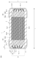
- FIG. 1 is a schematic perspective view of a laminated ceramic capacitor 1 of an embodiment
- FIG. 2 is a cross-sectional view of the multilayer ceramic capacitor 1 of FIG. 1 taken along line II-II.
- FIG. 2 is a cross-sectional view of the multilayer ceramic capacitor 1 of FIG. 1 taken along line III-III.
- FIG. 4 is a flow chart explaining an example of a method for manufacturing the multilayer ceramic capacitor 1.
- FIG. 3A to 3C are diagrams for explaining steps up to manufacturing a laminated sheet 103 in the manufacturing method of the multilayer ceramic capacitor 1.
- FIG. FIG. 3 is a diagram for explaining a lamination step in the manufacturing method of the multilayer ceramic capacitor 1;
- FIG. 1 is a schematic perspective view of a laminated ceramic capacitor 1 of an embodiment.
- FIG. 2 is a cross-sectional view of the multilayer ceramic capacitor 1 of FIG. 1 taken along line II-II.
- FIG. 3 is a cross-sectional view of the multilayer ceramic capacitor 1 of FIG. 1 taken along line III-III.
- a laminated ceramic capacitor 1 includes a laminate 2 and a pair of external electrodes 3 provided at both ends of the laminate 2 .
- the laminate 2 includes an inner layer portion 10 in which dielectric layers 11 and internal electrode layers 12 are alternately laminated.
- the direction in which the pair of external electrodes 3 are provided in the multilayer ceramic capacitor 1 is defined as the length direction L as a term that indicates the orientation of the multilayer ceramic capacitor 1 .
- the direction in which the dielectric layers 11 and the internal electrode layers 12 are stacked is defined as a stacking direction T.
- a direction crossing both the length direction L and the stacking direction T is defined as a width direction W.
- the width direction W is orthogonal to both the length direction L and the stacking direction T.
- the stacking direction T is also referred to as a thickness direction.
- the multilayer ceramic capacitor 1 has a withstand voltage of, for example, about 16V. It has a substantially rectangular parallelepiped shape, with a length direction L dimension of 0.09 mm or more and 1.1 mm, a width direction W dimension of 0.004 mm or more and 0.6 mm, and a thickness direction (stacking direction T) dimension of 0.004 mm. 0.6 mm or more.
- a pair of outer surfaces facing in the lamination direction T are referred to as a first main surface Aa and a second main surface Ab
- a pair of outer surfaces facing in the width direction W The outer surfaces are defined as a first side surface Ba and a second side surface Bb
- a pair of outer surfaces facing each other in the length direction L are defined as a first end surface Ca and a second end surface Cb.
- the first main surface Aa and the second main surface Ab they will be collectively referred to as the main surface A, and the first side surface Ba and the second side surface Bb will need to be specifically distinguished for explanation. If not, they will be collectively referred to as the side surface B, and the first end surface Ca and the second end surface Cb will be collectively described as the end surface C unless it is necessary to distinguish them for description.
- the laminate 2 includes an inner layer portion 10, outer layer portions 13 arranged on both sides of the inner layer portion 10 in the lamination direction T, and side gap portions 30 provided on both sides of the inner layer portion 10 and the outer layer portion 13 in the width direction W. and
- Inner layer portion 10 In the inner layer portion 10, dielectric layers 11 and internal electrode layers 12 are alternately laminated one by one.
- the dielectric layer 11 is formed by, for example, adding a binder, a plasticizer, a dispersant, etc. to a mixture obtained by adding and mixing a ceramic powder such as BaTiO 3 , a glass component, and a sintering aid as necessary.
- a ceramic green sheet obtained by molding a slurry containing an agent and an organic solvent into a sheet is sintered.
- the thickness of the dielectric layer 11 is, for example, 0.3 ⁇ m or more and 0.8 ⁇ m or less. Further, the number of dielectric layers 11 is 50 or more and 1000 or less.
- the internal electrode layer 12 is obtained by sintering an internal electrode layer paste containing a powder of the first metal component, which is the main component, a binder, additives such as a plasticizer and a dispersant, an organic solvent, and the like. is.
- the first metal component that is the main component of the internal electrode layer 12 is Ni in the embodiment, and the first metal component is hereinafter described as Ni.
- the internal electrode layers 12 include a plurality of first internal electrode layers 12A and a plurality of second internal electrode layers 12B.
- the first internal electrode layers 12A and the second internal electrode layers 12B are alternately arranged.
- the thickness of the internal electrode layer 12 is, for example, 0.3 ⁇ m or more and 0.8 ⁇ m or less.
- the number of internal electrode layers 12 is 50 or more and 1000 or less in total including the first internal electrode layers 12A and the second internal electrode layers 12B.
- the first internal electrode layer 12A includes a first facing portion 12Aa facing the second internal electrode layer 12B, and a first lead portion 12Ab drawn from the first facing portion 12Aa toward the first end surface Ca. An end portion of the first lead-out portion 12Ab is exposed on the first end surface Ca and electrically connected to a first external electrode 3A, which will be described later.
- the second internal electrode layer 12B includes a second facing portion 12Ba facing the first internal electrode layer 12A, and a second lead portion 12Bb drawn from the second facing portion 12Ba to the second end face Cb. An end portion of the second lead portion 12Bb is electrically connected to a second external electrode 3B, which will be described later. Charges are accumulated in the first facing portion 12Aa of the first internal electrode layer 12A and the second facing portion 12Ba of the second internal electrode layer 12B.
- first facing portion 12Aa and the second facing portion 12Ba do not need to be distinguished from each other, they will be collectively referred to as the facing portion 12a, and the first lead-out portion 12Ab and the second lead-out portion 12Bb will be specifically referred to. When there is no need to distinguish and explain, they will be collectively explained as the drawer portion 12b.
- FIG. 2 is a cross section extending in the stacking direction T and the length direction L through the central portion in the width direction W intersecting the stacking direction T and the length direction L.
- FIG. 2 is a cross section extending in the stacking direction T and the length direction L through the central portion in the width direction W intersecting the stacking direction T and the length direction L.
- the curved portion 121 is provided in an end region closer to the end face C than the position at the distance D1 from the end face C.
- the distance D1 is 5% or more and 20% or less or 10 ⁇ m or more and 50 ⁇ m or less of the lengthwise distance from the end surface C.
- the curved portion 121 curves toward the central portion in the stacking direction T as it goes from the facing portion 12a side toward the end face C. As shown in FIG.
- the degree of curvature of the curved portion 121 is the smallest in the central portion of the internal electrode layer 12 in the stacking direction T, and in the embodiment, the curved portion 121 of the internal electrode layer 12 in the center of the stacking direction T is substantially straight.
- the degree of curvature of the curved portion 121 increases toward the main surface A side. That is, the degree of curvature of the curved portion 121 of the internal electrode layer 12 closest to the main surface A is the largest. In other words, the curved portion 121 farthest in the stacking direction T from the central portion has the greatest degree of curvature.
- the distance D2 in the stacking direction T between the stacking direction T position of the end portion of the curved portion 121 on the side of the end surface C and the stacking direction T position of the opposing portion 12a is It is 5 ⁇ m or more and 50 ⁇ m or less.
- Solid solution layer 20 Furthermore, a second metal component different from the first metal component dissolves in Ni, which is the first metal component, at the interface with the dielectric layer 11 or the outer layer portion 13 on both sides of the internal electrode layer 12 in the stacking direction T.
- a solid solution layer 20 is provided.
- the solid solution layer 20 includes a first solid solution layer 21 and a second solid solution layer 22 .
- the second metal component is preferably Sn, In, Ga, Zn, Bi, Pb, Fe, V, Y, or Cu.
- the second metal component is Sn. Sn.
- the solid solution layer 20 is a layer in which Sn atoms are randomly substituted for Ni within the Ni atomic arrangement structure while maintaining the Ni atomic arrangement structure.
- the solid solution layer 20 has a thickness of 1 nm or more and 40 nm or less, preferably 1 nm or more and 20 nm or less.
- the solid solution layers 20 are provided at the interfaces on both sides of the internal electrode layers 12 in the stacking direction T, but the present invention is not limited to this. It may be provided only at the interface. In the embodiment, the solid solution layer 20 is provided on all the internal electrode layers 12 , but the present invention is not limited to this, and the solid solution layer 20 may be provided only on some of the internal electrode layers 12 .
- the first solid solution layer 21 is provided at the interface with the dielectric layer 11 or the outer layer portion 13 in the curved portion 121 .
- the present invention is not limited to this, in the first solid solution layer 21, 0.2 mol or more and 0.8 mol or less of Sn is dissolved in 100 mol of Ni.
- a value obtained by measuring 10 points by TEM analysis at the interface between the central portion in the stacking direction and the central portion in the width direction and averaging the values is used.
- the interface is not only a boundary, but also a region that may include a part of the internal electrode layer 12 and the dielectric layer 11 or the outer layer portion 13 .
- the first solid-solution layer 21 is provided only on the curved portion 121 of the internal electrode layer 12, but the present invention is not limited to this, and the first solid-solution layer 21 is provided on the uncurved portion of the lead portion 12b. Alternatively, it may extend to the outer peripheral region of the facing portion 12a.
- the second solid solution layer 22 is provided at the interface with the dielectric layer 11 or the outer layer portion 13 in the central region in the length direction L and width direction W of the facing portion 12a.
- the central region is a central region from a position of 10 ⁇ m or more and 100 ⁇ m or less from the outer circumference of the facing portion 12a.
- the central region in the lengthwise direction L and the widthwise direction W of the opposing portion 12 a is also the central region in the lengthwise direction L and the widthwise direction W of the laminate 2 .
- the concentration of Sn with respect to Ni in the second solid solution layer 22 is higher than that in the first solid solution layer 21 .
- the present invention is not limited to this, in the second solid solution layer 22, 1.5 mol or more and 2.5 mol or less of Sn is dissolved in 100 mol of Ni. 10 points of the interfaces in the central part in the stacking direction, the central part in the width direction, and the central part in the longitudinal direction are measured by TEM analysis, and the average value is used.
- the interface is not only a boundary, but also a region that may include a part of the internal electrode layer 12 and the dielectric layer 11 or the outer layer portion 13 .
- outer layer portion 13 The outer layer portions 13 are provided on both sides of the inner layer portion 10 in the stacking direction T, and are made of the same dielectric ceramic material as the dielectric layer 11 .
- the side gap portions 30 are provided on both sides of the inner layer portion 10 and the outer layer portion 13 in the width direction W, and are made of the same dielectric ceramic material as the dielectric layer 11 .
- the external electrodes 3 are provided on both end surfaces C of the laminate 2 .
- the external electrode 3 covers not only the end surface C, but also the main surface A and part of the side surface B on the end surface C side.
- the end of the first lead-out portion 12Ab of the first internal electrode layer 12A is exposed on the first end surface Ca and electrically connected to the first external electrode 3A.
- the end of the second lead-out portion 12Bb of the second internal electrode layer 12B is exposed on the second end surface Cb and electrically connected to the second external electrode 3B.
- a plurality of capacitor elements are electrically connected in parallel between the first external electrode 3A and the second external electrode 3B.
- FIG. 4 is a flow chart illustrating an example of a method for manufacturing the multilayer ceramic capacitor 1. As shown in FIG. This manufacturing method is an example, and the present invention is not limited to this.
- 5A and 5B are diagrams for explaining steps up to manufacturing a laminated sheet 103, which will be described later, in the manufacturing method of the multilayer ceramic capacitor 1.
- FIG. The process up to the production of this laminated sheet 103 is also an example, and the present invention is not limited to this.
- Ceramic green sheet production step S1 First, a ceramic slurry containing ceramic powder, a binder and a solvent is prepared. This ceramic slurry is printed in a sheet form on a carrier film using a die coater, a gravure coater, a micro gravure coater, or the like, to produce a ceramic green sheet 101 for the inner layer shown in FIG. 5(a).
- the first solid-soluble layer paste printing step S2 includes a first solid-soluble layer paste printing step S21 and a second solid-soluble layer paste printing step S22.
- first solid solution layer paste printing step S21 First, as shown in FIG. 5B, the first solid solution layer paste 21P is printed on the surface of the ceramic green sheet 101 for the inner layer portion.
- the first solid-solution layer paste 21P is printed on the end region of the lead-out portion forming region Pb that will eventually become the lead-out portion 12b.
- the first solid solution layer paste 21P contains 2.5 mol of Sn with respect to 100 mol of Ni.
- the second solid-solution layer paste 22P is printed on the surface of the ceramic green sheet 101 for the inner layer portion.
- the second solid-solution layer paste 22P is printed in the central portion of the facing portion forming region Pa, which will eventually become the facing portion 12a.
- the mol number of Sn contained in the second solid solution layer paste 22P per 100 mol of Ni is higher than the mol number of Sn contained in the first solid solution layer paste 21P per Ni.
- the second solid solution layer paste 22P contains 5 mol of Sn with respect to 100 mol of Ni.
- the other side paste printing step S4 also includes a first solid solution layer paste printing step S41 and a second solid solution layer paste printing step S42 similar to the one side solid solution layer paste printing step S2.
- FIG. 6 is a diagram for explaining the lamination process. As shown in the figure, a plurality of laminated sheets 103 are stacked such that the internal electrode forming regions P printed with the internal electrode layer paste 102 are shifted by half a pitch between adjacent laminated sheets 103 . Furthermore, ceramic green sheets 112 for outer layer portions are stacked on both sides of the laminated sheet 103 in which a plurality of laminated sheets are laminated.
- Thermal compression step S6 Subsequently, the ceramic green sheet 112 for the outer layer portion and the plurality of stacked laminated sheets 103 are thermocompression bonded. Thereby, the mother block 110 is formed.
- the internal electrode layer paste 102 of the laminated sheet 103 is printed in a region at a constant distance in the length direction L from the end face C of the laminated body 2 cut along the cutting line X.
- the printed portion and the unprinted portion are alternately laminated, and the internal electrode layer paste 102 in this portion becomes the lead portion 12b.
- the portion away from the end surface C by a certain distance or more only the portion of the laminated sheet 103 on which the internal electrode layer paste 102 is printed is laminated to form the facing portion 12a.
- the thickness in the stacking direction T is reduced in the area serving as the lead portion 12b. Therefore, a curved portion 121 that curves toward the end face C side is formed in the end region of the lead portion 12b on the end face C side.
- the laminate 2 having the external electrodes 3 formed thereon is heated at the set firing temperature in a nitrogen atmosphere for a predetermined time. Thereby, the multilayer ceramic capacitor 1 is manufactured. At this time, the ceramic green sheets 101 for the inner layer and the ceramic green sheets 112 for the outer layer are sintered into ceramics, and the dielectric layer 11 and the outer layer 13 are formed.
- the internal electrode layer paste 102 becomes the internal electrode layers 12.
- the first solid-solution layer paste 21P and the second solid-solution layer paste 22P printed on both sides of the internal electrode layer paste 102 in the stacking direction T are heated to form the first solid-solution layer 21 and the second solid-solution layer 22P, respectively. It becomes the solid solution layer 22 .
- the first solid solution layer 21 is formed at the interface with the dielectric layer 11 or the outer layer portion 13 in the end region of the lead portion 12b
- the second solid solution layer 22 is formed in the length direction L and the width It is formed at the interface with the dielectric layer 11 or the outer layer portion 13 in the central region in the direction W. As shown in FIG.
- the curved portion 121 is formed by deforming the drawer portion 12b by stacking and pressing the plurality of laminated sheets 103 in the laminating step S5 or the thermocompression bonding step S6.
- the strength of the portion of the drawn-out portion 12b where the curved portion 121 is formed may be reduced due to this deformation.
- the first solid solution layers 21 are formed at the interfaces on both sides of the curved portion 121 in the stacking direction T. As shown in FIG. Thereby, the strength of the curved portion 121 is improved, and the pressure resistance (voltage resistance) of the multilayer ceramic capacitor 1 is improved.
- a second solid solution layer 22 is formed at the interface with the dielectric layer 11 or the outer layer portion 13 in the central region in the length direction L and width direction W of the facing portion 12a.
- the solid solution of Sn in Ni changes the state (electrical barrier height) in the vicinity of the interface with the dielectric layer 11 in the curved portion 121, and the high-temperature load life can be improved. As described above, it is possible to obtain the multilayer ceramic capacitor 1 having excellent reliability when a voltage is applied.
Abstract
Provided is an electronic component with which high reliability can be obtained when a voltage is applied. This electronic component 1 is configured so that in an end region on an end-surface side of a position 5%–20% or 10 μm–50 μm distant in a length direction from an end surface of a lead section 12b of an inner electrode layer 12 of the electronic component: at an interface with a dielectric layer 11, a first solid solution layer 21 is provided in which a second metal constituent is put in solid solution in a first metal constituent that is a principal constituent of the inner electrode layer 12, the second metal constituent differing from the first metal constituent; and, in a central region, in the length direction and a width direction, of a facing section 12a, at an interface with the dielectric layer 11, a second solid solution layer 22 is provided in which the second metal constituent is put in solid solution in the first metal constituent at a higher concentration than in the first solid solution layer 21.
Description
本発明は、電子部品に関する。
The present invention relates to electronic components.
例えば積層セラミックコンデンサである電子部品は、複数の誘電体層と複数の内部電極層とが互いに交互に積層された積層体と、積層体における、長さ方向の両側に設けられた2つの端面にそれぞれ配置された2つの外部電極と、を備える(特許文献1参照)。
For example, an electronic component, which is a multilayer ceramic capacitor, includes a laminate in which a plurality of dielectric layers and a plurality of internal electrode layers are alternately laminated, and two end faces provided on both sides in the length direction of the laminate. and two external electrodes arranged respectively (see Patent Document 1).
このような電子部品は、電圧印加時における高い信頼性が求められている。本発明は、電圧印加時における高い信頼性が得られる電子部品を提供することを目的とする。
Such electronic components are required to have high reliability when voltage is applied. SUMMARY OF THE INVENTION An object of the present invention is to provide an electronic component that is highly reliable when a voltage is applied.
上記課題を解決するために、本発明は、複数の誘電体層と複数の内部電極層とが互いに交互に積層された積層体と、前記積層体における、長さ方向の両側に設けられた2つの端面にそれぞれ配置された2つの外部電極と、を備え、前記内部電極層は、積層方向に隣り合う他の内部電極層と対向する対向部、及び、該対向部から一方の前記端面に延びて該一方の前記端面に配置された前記外部電極と接続する引出部、を有する第1内部電極層と、前記対向部、及び、該対向部から他方の前記端面に延びて該他方の前記端面に配置された前記外部電極と接続する引出部を有する第2内部電極層と、が互いに交互に配置され、前記引出部における、前記端面から長さ方向距離の5%以上20%以下もしくは10μm以上50μm以下の位置より前記端面側の端部領域には、前記誘電体層との界面に、前記内部電極層の主成分である第1金属成分に、該第1金属成分と異なる第2金属成分が固溶している第1固溶層が設けられ、前記対向部における、前記長さ方向及び幅方向の中央領域には、前記誘電体層との界面に、前記第1金属成分に、前記第2金属成分が、前記第1固溶層より高い濃度で固溶している、第2固溶層が設けられている電子部品を提供する。
In order to solve the above problems, the present invention provides a laminate in which a plurality of dielectric layers and a plurality of internal electrode layers are alternately laminated, and two electrodes provided on both sides in the length direction of the laminate. and two external electrodes respectively arranged on two end faces, wherein the internal electrode layer has a facing portion facing another internal electrode layer adjacent in the stacking direction, and extends from the facing portion to one of the end faces. a first internal electrode layer having a lead portion connected to the external electrode disposed on the one end face; the opposing portion; and a second internal electrode layer having lead portions connected to the external electrodes arranged alternately, and the length direction distance of the lead portions from the end surface is 5% or more and 20% or less, or 10 μm or more. A first metal component, which is the main component of the internal electrode layer, and a second metal component different from the first metal component are added to the interface with the dielectric layer in the end region on the side of the end face from a position of 50 μm or less. is provided in a solid solution, and in the central region in the length direction and the width direction of the facing portion, at the interface with the dielectric layer, at the first metal component, at the interface with the Provided is an electronic component provided with a second solid solution layer in which a second metal component is dissolved in a higher concentration than the first solid solution layer.
本発明によれば、電圧印加時における高い信頼性が得られる電子部品を提供することができる。
According to the present invention, it is possible to provide an electronic component with high reliability when voltage is applied.
以下、本発明の実施形態にかかる積層セラミックコンデンサ1について説明する。図1は、実施形態の積層セラミックコンデンサ1の概略斜視図である。図2は、図1の積層セラミックコンデンサ1のII-II線に沿った断面図である。図3は、図1の積層セラミックコンデンサ1のIII-III線に沿った断面図である。
A laminated ceramic capacitor 1 according to an embodiment of the present invention will be described below. FIG. 1 is a schematic perspective view of a laminated ceramic capacitor 1 of an embodiment. FIG. 2 is a cross-sectional view of the multilayer ceramic capacitor 1 of FIG. 1 taken along line II-II. FIG. 3 is a cross-sectional view of the multilayer ceramic capacitor 1 of FIG. 1 taken along line III-III.
積層セラミックコンデンサ1は、積層体2と、積層体2の両端に設けられた一対の外部電極3とを備える。積層体2は、誘電体層11と内部電極層12とが、互いに交互に積層された内層部10を含む。
A laminated ceramic capacitor 1 includes a laminate 2 and a pair of external electrodes 3 provided at both ends of the laminate 2 . The laminate 2 includes an inner layer portion 10 in which dielectric layers 11 and internal electrode layers 12 are alternately laminated.
以下の説明において、積層セラミックコンデンサ1の向きを表わす用語として、積層セラミックコンデンサ1において、一対の外部電極3が設けられている方向を長さ方向Lとする。誘電体層11と内部電極層12とが積層されている方向を積層方向Tとする。長さ方向L及び積層方向Tのいずれにも交差する方向を幅方向Wとする。なお、実施形態においては、幅方向Wは長さ方向L及び積層方向Tのいずれにも直交している。また、積層方向Tを厚み方向ともいう。
In the following description, the direction in which the pair of external electrodes 3 are provided in the multilayer ceramic capacitor 1 is defined as the length direction L as a term that indicates the orientation of the multilayer ceramic capacitor 1 . The direction in which the dielectric layers 11 and the internal electrode layers 12 are stacked is defined as a stacking direction T. As shown in FIG. A direction crossing both the length direction L and the stacking direction T is defined as a width direction W. As shown in FIG. In addition, in the embodiment, the width direction W is orthogonal to both the length direction L and the stacking direction T. As shown in FIG. Moreover, the stacking direction T is also referred to as a thickness direction.
積層セラミックコンデンサ1は、例えば、耐電圧が16V程度である。そして、略直方体形状を有し、長さ方向L寸法が、0.09mm以上1.1mm、幅方向W寸法が、0.004mm以上0.6mm、厚み方向(積層方向T)寸法が0.004mm以上0.6mmである。
The multilayer ceramic capacitor 1 has a withstand voltage of, for example, about 16V. It has a substantially rectangular parallelepiped shape, with a length direction L dimension of 0.09 mm or more and 1.1 mm, a width direction W dimension of 0.004 mm or more and 0.6 mm, and a thickness direction (stacking direction T) dimension of 0.004 mm. 0.6 mm or more.
また、以下の説明において、積層体2の6つの外表面のうち、積層方向Tに相対する一対の外表面を第1主面Aaと第2主面Abとし、幅方向Wに相対する一対の外表面を第1側面Baと第2側面Bbとし、長さ方向Lに相対する一対の外表面を第1端面Caと第2端面Cbとする。なお、第1主面Aaと第2主面Abとを特に区別して説明する必要のない場合、まとめて主面Aとし、第1側面Baと第2側面Bbとを特に区別して説明する必要のない場合、まとめて側面Bとし、第1端面Caと第2端面Cbとを特に区別して説明する必要のない場合、まとめて端面Cとして説明する。
Further, in the following description, of the six outer surfaces of the laminate 2, a pair of outer surfaces facing in the lamination direction T are referred to as a first main surface Aa and a second main surface Ab, and a pair of outer surfaces facing in the width direction W The outer surfaces are defined as a first side surface Ba and a second side surface Bb, and a pair of outer surfaces facing each other in the length direction L are defined as a first end surface Ca and a second end surface Cb. In addition, when it is not necessary to specifically distinguish between the first main surface Aa and the second main surface Ab, they will be collectively referred to as the main surface A, and the first side surface Ba and the second side surface Bb will need to be specifically distinguished for explanation. If not, they will be collectively referred to as the side surface B, and the first end surface Ca and the second end surface Cb will be collectively described as the end surface C unless it is necessary to distinguish them for description.
(積層体2)
積層体2は、内層部10と、内層部10の積層方向Tの両側にそれぞれ配置された外層部13と、内層部10及び外層部13の幅方向Wの両側に設けられたサイドギャップ部30とを備える。 (Laminate 2)
Thelaminate 2 includes an inner layer portion 10, outer layer portions 13 arranged on both sides of the inner layer portion 10 in the lamination direction T, and side gap portions 30 provided on both sides of the inner layer portion 10 and the outer layer portion 13 in the width direction W. and
積層体2は、内層部10と、内層部10の積層方向Tの両側にそれぞれ配置された外層部13と、内層部10及び外層部13の幅方向Wの両側に設けられたサイドギャップ部30とを備える。 (Laminate 2)
The
(内層部10)
内層部10は、誘電体層11と内部電極層12とが、1枚ずつ交互に積層されている。 (Inner layer portion 10)
In theinner layer portion 10, dielectric layers 11 and internal electrode layers 12 are alternately laminated one by one.
内層部10は、誘電体層11と内部電極層12とが、1枚ずつ交互に積層されている。 (Inner layer portion 10)
In the
(誘電体層11)
誘電体層11は、例えば、BaTiO3であるセラミック粉末と、ガラス成分と、必要に応じて焼結助剤と、を添加して混合した混合物に、バインダと、可塑剤や分散剤等の添加剤と、有機溶剤と、を加えたスラリーをシート状に成形して得られたセラミックグリーンシートが焼結されたものである。誘電体層11の厚みは、例えば、0.3μm以上0.8μm以下である。また、誘電体層11の枚数は、50枚以上1000枚以下である。 (Dielectric layer 11)
Thedielectric layer 11 is formed by, for example, adding a binder, a plasticizer, a dispersant, etc. to a mixture obtained by adding and mixing a ceramic powder such as BaTiO 3 , a glass component, and a sintering aid as necessary. A ceramic green sheet obtained by molding a slurry containing an agent and an organic solvent into a sheet is sintered. The thickness of the dielectric layer 11 is, for example, 0.3 μm or more and 0.8 μm or less. Further, the number of dielectric layers 11 is 50 or more and 1000 or less.
誘電体層11は、例えば、BaTiO3であるセラミック粉末と、ガラス成分と、必要に応じて焼結助剤と、を添加して混合した混合物に、バインダと、可塑剤や分散剤等の添加剤と、有機溶剤と、を加えたスラリーをシート状に成形して得られたセラミックグリーンシートが焼結されたものである。誘電体層11の厚みは、例えば、0.3μm以上0.8μm以下である。また、誘電体層11の枚数は、50枚以上1000枚以下である。 (Dielectric layer 11)
The
(内部電極層12)
内部電極層12は、主成分である第1金属成分の粉末と、バインダと、可塑剤や分散剤等の添加剤と、有機溶剤と、等を含む内部電極層用ペーストが焼結されたものである。内部電極層12の主成分である第1金属成分は、実施形態ではNiであり、以下、第1金属成分をNiとして説明する。 (Internal electrode layer 12)
Theinternal electrode layer 12 is obtained by sintering an internal electrode layer paste containing a powder of the first metal component, which is the main component, a binder, additives such as a plasticizer and a dispersant, an organic solvent, and the like. is. The first metal component that is the main component of the internal electrode layer 12 is Ni in the embodiment, and the first metal component is hereinafter described as Ni.
内部電極層12は、主成分である第1金属成分の粉末と、バインダと、可塑剤や分散剤等の添加剤と、有機溶剤と、等を含む内部電極層用ペーストが焼結されたものである。内部電極層12の主成分である第1金属成分は、実施形態ではNiであり、以下、第1金属成分をNiとして説明する。 (Internal electrode layer 12)
The
内部電極層12は、複数の第1内部電極層12Aと複数の第2内部電極層12Bとを備える。第1内部電極層12Aと第2内部電極層12Bとは、交互に配置されている。内部電極層12の厚みは、例えば、0.3μm以上0.8μm以下である。また、内部電極層12の枚数は、第1内部電極層12A及び第2内部電極層12Bを合わせて50枚以上1000枚以下である。
The internal electrode layers 12 include a plurality of first internal electrode layers 12A and a plurality of second internal electrode layers 12B. The first internal electrode layers 12A and the second internal electrode layers 12B are alternately arranged. The thickness of the internal electrode layer 12 is, for example, 0.3 μm or more and 0.8 μm or less. In addition, the number of internal electrode layers 12 is 50 or more and 1000 or less in total including the first internal electrode layers 12A and the second internal electrode layers 12B.
第1内部電極層12Aは、第2内部電極層12Bと対向する第1対向部12Aaと、第1対向部12Aaから第1端面Ca側に引き出された第1引出部12Abとを備える。第1引出部12Abの端部は、第1端面Caに露出し、後述の第1外部電極3Aに電気的に接続されている。
第2内部電極層12Bは、第1内部電極層12Aと対向する第2対向部12Baと、第2対向部12Baから第2端面Cbに引き出された第2引出部12Bbとを備える。第2引出部12Bbの端部は、後述の第2外部電極3Bに電気的に接続されている。そして、第1内部電極層12Aの第1対向部12Aaと、第2内部電極層12Bの第2対向部12Baとに電荷が蓄積される。 The firstinternal electrode layer 12A includes a first facing portion 12Aa facing the second internal electrode layer 12B, and a first lead portion 12Ab drawn from the first facing portion 12Aa toward the first end surface Ca. An end portion of the first lead-out portion 12Ab is exposed on the first end surface Ca and electrically connected to a first external electrode 3A, which will be described later.
The secondinternal electrode layer 12B includes a second facing portion 12Ba facing the first internal electrode layer 12A, and a second lead portion 12Bb drawn from the second facing portion 12Ba to the second end face Cb. An end portion of the second lead portion 12Bb is electrically connected to a second external electrode 3B, which will be described later. Charges are accumulated in the first facing portion 12Aa of the first internal electrode layer 12A and the second facing portion 12Ba of the second internal electrode layer 12B.
第2内部電極層12Bは、第1内部電極層12Aと対向する第2対向部12Baと、第2対向部12Baから第2端面Cbに引き出された第2引出部12Bbとを備える。第2引出部12Bbの端部は、後述の第2外部電極3Bに電気的に接続されている。そして、第1内部電極層12Aの第1対向部12Aaと、第2内部電極層12Bの第2対向部12Baとに電荷が蓄積される。 The first
The second
なお、以下、第1対向部12Aaと第2対向部12Baとを特に区別して説明する必要のない場合、まとめて対向部12aとして説明し、第1引出部12Abと第2引出部12Bbとを特に区別して説明する必要のない場合、まとめて引出部12bとして説明する。
In the following description, when the first facing portion 12Aa and the second facing portion 12Ba do not need to be distinguished from each other, they will be collectively referred to as the facing portion 12a, and the first lead-out portion 12Ab and the second lead-out portion 12Bb will be specifically referred to. When there is no need to distinguish and explain, they will be collectively explained as the drawer portion 12b.
(湾曲部121)
内部電極層12の引出部12bには、湾曲部121が設けられている。図2は、積層方向T及び長さ方向Lと交差する幅方向Wの中央部を通り、且つ積層方向T及び長さ方向Lに延びる断面である。図2に示すように、湾曲部121は、端面Cから距離D1の位置よりも端面C側の端部領域に設けられている。距離D1は、端面Cから長さ方向距離の5%以上20%以下もしくは10μm以上50μm以下の位置である。そして、湾曲部121は、対向部12a側から端面Cに向かうに従い、積層方向Tの中央部に向かって湾曲している。 (Bending portion 121)
Acurved portion 121 is provided in the lead portion 12 b of the internal electrode layer 12 . FIG. 2 is a cross section extending in the stacking direction T and the length direction L through the central portion in the width direction W intersecting the stacking direction T and the length direction L. FIG. As shown in FIG. 2, the curved portion 121 is provided in an end region closer to the end face C than the position at the distance D1 from the end face C. As shown in FIG. The distance D1 is 5% or more and 20% or less or 10 μm or more and 50 μm or less of the lengthwise distance from the end surface C. The curved portion 121 curves toward the central portion in the stacking direction T as it goes from the facing portion 12a side toward the end face C. As shown in FIG.
内部電極層12の引出部12bには、湾曲部121が設けられている。図2は、積層方向T及び長さ方向Lと交差する幅方向Wの中央部を通り、且つ積層方向T及び長さ方向Lに延びる断面である。図2に示すように、湾曲部121は、端面Cから距離D1の位置よりも端面C側の端部領域に設けられている。距離D1は、端面Cから長さ方向距離の5%以上20%以下もしくは10μm以上50μm以下の位置である。そして、湾曲部121は、対向部12a側から端面Cに向かうに従い、積層方向Tの中央部に向かって湾曲している。 (Bending portion 121)
A
湾曲部121の湾曲の程度は、積層方向Tの中央部の内部電極層12が一番小さく、実施形態において、積層方向T中央の内部電極層12の湾曲部121は略直線である。そして、湾曲部121の湾曲の程度は、主面A側に向かうにつれて大きくなる。すなわち、最も主面A側の内部電極層12の湾曲部121の湾曲の程度が最も大きい。換言すると、中央部から積層方向Tに最も離れた湾曲部121の湾曲の程度が最も大きい。最も主面A側に位置する内部電極層12における、湾曲部121の端面C側端部の積層方向T位置と、対向部12aの積層方向T位置との間の積層方向Tの距離D2は、5μm以上50μm以下である。
The degree of curvature of the curved portion 121 is the smallest in the central portion of the internal electrode layer 12 in the stacking direction T, and in the embodiment, the curved portion 121 of the internal electrode layer 12 in the center of the stacking direction T is substantially straight. The degree of curvature of the curved portion 121 increases toward the main surface A side. That is, the degree of curvature of the curved portion 121 of the internal electrode layer 12 closest to the main surface A is the largest. In other words, the curved portion 121 farthest in the stacking direction T from the central portion has the greatest degree of curvature. In the internal electrode layer 12 located closest to the main surface A, the distance D2 in the stacking direction T between the stacking direction T position of the end portion of the curved portion 121 on the side of the end surface C and the stacking direction T position of the opposing portion 12a is It is 5 μm or more and 50 μm or less.
(固溶層20)
さらに、内部電極層12の積層方向Tの両側の、誘電体層11又は外層部13との界面には、第1金属成分であるNiに、第1金属成分と異なる第2金属成分が固溶した固溶層20が設けられている。固溶層20は第1固溶層21と第2固溶層22とを含む。第2金属成分は、Sn、In、Ga、Zn、Bi、Pb、Fe、V、Y、Cuのであることが好ましく、実施形態で第2金属成分はSnであり、以下、第2金属成分をSnとして説明する。なお、固溶層20とは、Niの原子配列構造を保持しながら、Snの原子がNiの原子配列構造内においてランダムにNiから置換している層である。固溶層20の厚みは1nm以上40nm以下であり、1nm以上20nmであることが好ましい。 (Solid solution layer 20)
Furthermore, a second metal component different from the first metal component dissolves in Ni, which is the first metal component, at the interface with thedielectric layer 11 or the outer layer portion 13 on both sides of the internal electrode layer 12 in the stacking direction T. A solid solution layer 20 is provided. The solid solution layer 20 includes a first solid solution layer 21 and a second solid solution layer 22 . The second metal component is preferably Sn, In, Ga, Zn, Bi, Pb, Fe, V, Y, or Cu. In the embodiment, the second metal component is Sn. Sn. The solid solution layer 20 is a layer in which Sn atoms are randomly substituted for Ni within the Ni atomic arrangement structure while maintaining the Ni atomic arrangement structure. The solid solution layer 20 has a thickness of 1 nm or more and 40 nm or less, preferably 1 nm or more and 20 nm or less.
さらに、内部電極層12の積層方向Tの両側の、誘電体層11又は外層部13との界面には、第1金属成分であるNiに、第1金属成分と異なる第2金属成分が固溶した固溶層20が設けられている。固溶層20は第1固溶層21と第2固溶層22とを含む。第2金属成分は、Sn、In、Ga、Zn、Bi、Pb、Fe、V、Y、Cuのであることが好ましく、実施形態で第2金属成分はSnであり、以下、第2金属成分をSnとして説明する。なお、固溶層20とは、Niの原子配列構造を保持しながら、Snの原子がNiの原子配列構造内においてランダムにNiから置換している層である。固溶層20の厚みは1nm以上40nm以下であり、1nm以上20nmであることが好ましい。 (Solid solution layer 20)
Furthermore, a second metal component different from the first metal component dissolves in Ni, which is the first metal component, at the interface with the
実施形態では内部電極層12の積層方向Tの両側の界面に固溶層20が設けられているが、これに限らず、固溶層20は、内部電極層12の積層方向Tの一側の界面のみに設けられていてもよい。また、実施形態では全ての内部電極層12に固溶層20が設けられているが、これに限らず、固溶層20は、一部の内部電極層12のみに設けられていてもよい。
In the embodiment, the solid solution layers 20 are provided at the interfaces on both sides of the internal electrode layers 12 in the stacking direction T, but the present invention is not limited to this. It may be provided only at the interface. In the embodiment, the solid solution layer 20 is provided on all the internal electrode layers 12 , but the present invention is not limited to this, and the solid solution layer 20 may be provided only on some of the internal electrode layers 12 .
(第1固溶層21)
第1固溶層21は、湾曲部121における、誘電体層11又は外層部13との界面に設けられている。本発明はこれに限定されないが、第1固溶層21は、Ni100molに対して、Snが0.2mol以上0.8mol以下固溶している。積層方向中央部、幅方向中央部の界面をTEM分析にて、10点測定し、平均値化した値を用いている。ここで、界面とは境界を示すだけでなく、内部電極層12と誘電体層11又は外層部13の一部を含んでもよい領域である。 (First solid solution layer 21)
The first solid solution layer 21 is provided at the interface with thedielectric layer 11 or the outer layer portion 13 in the curved portion 121 . Although the present invention is not limited to this, in the first solid solution layer 21, 0.2 mol or more and 0.8 mol or less of Sn is dissolved in 100 mol of Ni. A value obtained by measuring 10 points by TEM analysis at the interface between the central portion in the stacking direction and the central portion in the width direction and averaging the values is used. Here, the interface is not only a boundary, but also a region that may include a part of the internal electrode layer 12 and the dielectric layer 11 or the outer layer portion 13 .
第1固溶層21は、湾曲部121における、誘電体層11又は外層部13との界面に設けられている。本発明はこれに限定されないが、第1固溶層21は、Ni100molに対して、Snが0.2mol以上0.8mol以下固溶している。積層方向中央部、幅方向中央部の界面をTEM分析にて、10点測定し、平均値化した値を用いている。ここで、界面とは境界を示すだけでなく、内部電極層12と誘電体層11又は外層部13の一部を含んでもよい領域である。 (First solid solution layer 21)
The first solid solution layer 21 is provided at the interface with the
実施形態で第1固溶層21は、内部電極層12における湾曲部121にのみに設けられているが、これに限らず、第1固溶層21は、引出部12bの湾曲していない部分や、対向部12aの外周領域まで延びていてもよい。
In the embodiment, the first solid-solution layer 21 is provided only on the curved portion 121 of the internal electrode layer 12, but the present invention is not limited to this, and the first solid-solution layer 21 is provided on the uncurved portion of the lead portion 12b. Alternatively, it may extend to the outer peripheral region of the facing portion 12a.
(第2固溶層22)
第2固溶層22は、対向部12aの長さ方向L及び幅方向Wの中央領域における、誘電体層11又は外層部13との界面に設けられている。中央領域は、対向部12aの外周からの10μm以上100μm以下の位置よりも中央の領域である。なお、対向部12aの長さ方向L及び幅方向Wの中央領域とは、積層体2の長さ方向L及び幅方向Wの中央領域でもある。 (Second solid solution layer 22)
The second solid solution layer 22 is provided at the interface with thedielectric layer 11 or the outer layer portion 13 in the central region in the length direction L and width direction W of the facing portion 12a. The central region is a central region from a position of 10 μm or more and 100 μm or less from the outer circumference of the facing portion 12a. The central region in the lengthwise direction L and the widthwise direction W of the opposing portion 12 a is also the central region in the lengthwise direction L and the widthwise direction W of the laminate 2 .
第2固溶層22は、対向部12aの長さ方向L及び幅方向Wの中央領域における、誘電体層11又は外層部13との界面に設けられている。中央領域は、対向部12aの外周からの10μm以上100μm以下の位置よりも中央の領域である。なお、対向部12aの長さ方向L及び幅方向Wの中央領域とは、積層体2の長さ方向L及び幅方向Wの中央領域でもある。 (Second solid solution layer 22)
The second solid solution layer 22 is provided at the interface with the
第2固溶層22における、Niに対するSnの濃度は、第1固溶層21より高い。本発明はこれに限定されないが、第2固溶層22は、Ni100molに対してSnが1.5mol以上2.5mol以下で固溶している。積層方向中央部、幅方向中央部および長さ方向中央部の界面をTEM分析にて、10点測定し、平均値化した値を用いている。ここで、界面とは境界を示すだけでなく、内部電極層12と誘電体層11又は外層部13の一部を含んでもよい領域である。
The concentration of Sn with respect to Ni in the second solid solution layer 22 is higher than that in the first solid solution layer 21 . Although the present invention is not limited to this, in the second solid solution layer 22, 1.5 mol or more and 2.5 mol or less of Sn is dissolved in 100 mol of Ni. 10 points of the interfaces in the central part in the stacking direction, the central part in the width direction, and the central part in the longitudinal direction are measured by TEM analysis, and the average value is used. Here, the interface is not only a boundary, but also a region that may include a part of the internal electrode layer 12 and the dielectric layer 11 or the outer layer portion 13 .
(外層部13)
外層部13は、内層部10の積層方向Tの両側にそれぞれ設けられ、誘電体層11と同じ、誘電体セラミック材料で製造されている。 (Outer layer portion 13)
Theouter layer portions 13 are provided on both sides of the inner layer portion 10 in the stacking direction T, and are made of the same dielectric ceramic material as the dielectric layer 11 .
外層部13は、内層部10の積層方向Tの両側にそれぞれ設けられ、誘電体層11と同じ、誘電体セラミック材料で製造されている。 (Outer layer portion 13)
The
(サイドギャップ部30)
サイドギャップ部30は、内層部10及び外層部13の幅方向Wの両側に設けられ、誘電体層11と同じ、誘電体セラミック材料で製造されている。 (Side gap portion 30)
Theside gap portions 30 are provided on both sides of the inner layer portion 10 and the outer layer portion 13 in the width direction W, and are made of the same dielectric ceramic material as the dielectric layer 11 .
サイドギャップ部30は、内層部10及び外層部13の幅方向Wの両側に設けられ、誘電体層11と同じ、誘電体セラミック材料で製造されている。 (Side gap portion 30)
The
(外部電極3)
外部電極3は、積層体2の両方の端面Cに設けられている。外部電極3は、端面Cだけでなく、主面A及び側面Bの端面C側の一部も覆っている。 (External electrode 3)
Theexternal electrodes 3 are provided on both end surfaces C of the laminate 2 . The external electrode 3 covers not only the end surface C, but also the main surface A and part of the side surface B on the end surface C side.
外部電極3は、積層体2の両方の端面Cに設けられている。外部電極3は、端面Cだけでなく、主面A及び側面Bの端面C側の一部も覆っている。 (External electrode 3)
The
上述のように、第1内部電極層12Aの第1引出部12Abの端部は第1端面Caに露出し、第1外部電極3Aに電気的に接続されている。また、第2内部電極層12Bの第2引出部12Bbの端部は第2端面Cbに露出し、第2外部電極3Bに電気的に接続されている。これにより、第1外部電極3Aと第2外部電極3Bとの間は、複数のコンデンサ要素が電気的に並列に接続された構造となっている。
As described above, the end of the first lead-out portion 12Ab of the first internal electrode layer 12A is exposed on the first end surface Ca and electrically connected to the first external electrode 3A. Also, the end of the second lead-out portion 12Bb of the second internal electrode layer 12B is exposed on the second end surface Cb and electrically connected to the second external electrode 3B. As a result, a plurality of capacitor elements are electrically connected in parallel between the first external electrode 3A and the second external electrode 3B.
(製造工程)
図4は、積層セラミックコンデンサ1の製造方法の一例を説明するフローチャートである。なお、この製造方法は一例であって、本発明はこれに限定されるものではない。図5は、積層セラミックコンデンサ1の製造方法における、後述の積層シート103を作製するまでの工程を説明する図である。この積層シート103を作製するまでの工程も、一例であって、本発明はこれに限定されるものではない。 (Manufacturing process)
FIG. 4 is a flow chart illustrating an example of a method for manufacturing the multilayerceramic capacitor 1. As shown in FIG. This manufacturing method is an example, and the present invention is not limited to this. 5A and 5B are diagrams for explaining steps up to manufacturing a laminated sheet 103, which will be described later, in the manufacturing method of the multilayer ceramic capacitor 1. FIG. The process up to the production of this laminated sheet 103 is also an example, and the present invention is not limited to this.
図4は、積層セラミックコンデンサ1の製造方法の一例を説明するフローチャートである。なお、この製造方法は一例であって、本発明はこれに限定されるものではない。図5は、積層セラミックコンデンサ1の製造方法における、後述の積層シート103を作製するまでの工程を説明する図である。この積層シート103を作製するまでの工程も、一例であって、本発明はこれに限定されるものではない。 (Manufacturing process)
FIG. 4 is a flow chart illustrating an example of a method for manufacturing the multilayer
(セラミックグリーンシート作製工程S1)
まず、セラミックス粉末、バインダ及び溶剤を含むセラミックスラリーが準備される。このセラミックスラリーがキャリアフィルム上においてダイコータ、グラビアコータ、マイクログラビアコータ等を用いてシート状に印刷されることで、図5(a)に示す内層部用セラミックグリーンシート101が作製される。 (Ceramic green sheet production step S1)
First, a ceramic slurry containing ceramic powder, a binder and a solvent is prepared. This ceramic slurry is printed in a sheet form on a carrier film using a die coater, a gravure coater, a micro gravure coater, or the like, to produce a ceramicgreen sheet 101 for the inner layer shown in FIG. 5(a).
まず、セラミックス粉末、バインダ及び溶剤を含むセラミックスラリーが準備される。このセラミックスラリーがキャリアフィルム上においてダイコータ、グラビアコータ、マイクログラビアコータ等を用いてシート状に印刷されることで、図5(a)に示す内層部用セラミックグリーンシート101が作製される。 (Ceramic green sheet production step S1)
First, a ceramic slurry containing ceramic powder, a binder and a solvent is prepared. This ceramic slurry is printed in a sheet form on a carrier film using a die coater, a gravure coater, a micro gravure coater, or the like, to produce a ceramic
(一面側固溶層用ペースト印刷工程S2)
一面側固溶層用ペースト印刷工程S2は、第1固溶層用ペースト印刷工程S21と、第2固溶層用ペースト印刷工程S22とを含む。 (Paste printing step S2 for solid solution layer on one side)
The first solid-soluble layer paste printing step S2 includes a first solid-soluble layer paste printing step S21 and a second solid-soluble layer paste printing step S22.
一面側固溶層用ペースト印刷工程S2は、第1固溶層用ペースト印刷工程S21と、第2固溶層用ペースト印刷工程S22とを含む。 (Paste printing step S2 for solid solution layer on one side)
The first solid-soluble layer paste printing step S2 includes a first solid-soluble layer paste printing step S21 and a second solid-soluble layer paste printing step S22.
(第1固溶層用ペースト印刷工程S21)
まず、図5(b)に示すように、内層部用セラミックグリーンシート101の表面に第1固溶層用ペースト21Pが印刷される。第1固溶層用ペースト21Pは、最終的に引出部12bとなる引出部形成領域Pbの端部領域に印刷される。実施形態で第1固溶層用ペースト21Pは、Ni100molに対してSnを2.5mol含む。 (First solid solution layer paste printing step S21)
First, as shown in FIG. 5B, the first solidsolution layer paste 21P is printed on the surface of the ceramic green sheet 101 for the inner layer portion. The first solid-solution layer paste 21P is printed on the end region of the lead-out portion forming region Pb that will eventually become the lead-out portion 12b. In the embodiment, the first solid solution layer paste 21P contains 2.5 mol of Sn with respect to 100 mol of Ni.
まず、図5(b)に示すように、内層部用セラミックグリーンシート101の表面に第1固溶層用ペースト21Pが印刷される。第1固溶層用ペースト21Pは、最終的に引出部12bとなる引出部形成領域Pbの端部領域に印刷される。実施形態で第1固溶層用ペースト21Pは、Ni100molに対してSnを2.5mol含む。 (First solid solution layer paste printing step S21)
First, as shown in FIG. 5B, the first solid
(第2固溶層用ペースト印刷工程S22)
続いて、図5(c)に示すように、内層部用セラミックグリーンシート101の表面に第2固溶層用ペースト22Pが印刷される。第2固溶層用ペースト22Pは、最終的に対向部12aとなる対向部形成領域Paの中央部に印刷される。第2固溶層用ペースト22Pに含まれるSnのNi100molに対するmol数は、第1固溶層用ペースト21Pに含まれるSnのNiに対するmol数より高い。実施形態で第2固溶層用ペースト22Pは、Ni100molに対してSnを5mol含む。 (Paste printing step S22 for second solid solution layer)
Subsequently, as shown in FIG. 5C, the second solid-solution layer paste 22P is printed on the surface of the ceramic green sheet 101 for the inner layer portion. The second solid-solution layer paste 22P is printed in the central portion of the facing portion forming region Pa, which will eventually become the facing portion 12a. The mol number of Sn contained in the second solid solution layer paste 22P per 100 mol of Ni is higher than the mol number of Sn contained in the first solid solution layer paste 21P per Ni. In the embodiment, the second solid solution layer paste 22P contains 5 mol of Sn with respect to 100 mol of Ni.
続いて、図5(c)に示すように、内層部用セラミックグリーンシート101の表面に第2固溶層用ペースト22Pが印刷される。第2固溶層用ペースト22Pは、最終的に対向部12aとなる対向部形成領域Paの中央部に印刷される。第2固溶層用ペースト22Pに含まれるSnのNi100molに対するmol数は、第1固溶層用ペースト21Pに含まれるSnのNiに対するmol数より高い。実施形態で第2固溶層用ペースト22Pは、Ni100molに対してSnを5mol含む。 (Paste printing step S22 for second solid solution layer)
Subsequently, as shown in FIG. 5C, the second solid-
(内部電極層用ペースト印刷工程S3)
次いで、図5(d)に示すように、第1固溶層用ペースト21P及び第2固溶層用ペースト22Pが印刷された、引出部形成領域Pbと対向部形成領域Paとを足した内部電極形成領域Pに、内部電極層12となる内部電極層用ペースト102が印刷される。 (Internal electrode layer paste printing step S3)
Next, as shown in FIG. 5(d), the inside of the lead portion forming region Pb and the facing portion forming region Pa on which the first solid-solution layer paste 21P and the second solid-solution layer paste 22P are printed An internal electrode layer paste 102 that will become the internal electrode layers 12 is printed on the electrode forming region P. As shown in FIG.
次いで、図5(d)に示すように、第1固溶層用ペースト21P及び第2固溶層用ペースト22Pが印刷された、引出部形成領域Pbと対向部形成領域Paとを足した内部電極形成領域Pに、内部電極層12となる内部電極層用ペースト102が印刷される。 (Internal electrode layer paste printing step S3)
Next, as shown in FIG. 5(d), the inside of the lead portion forming region Pb and the facing portion forming region Pa on which the first solid-
(他面側用ペースト印刷工程S4)
他面側用ペースト印刷工程S4も、一面側固溶層用ペースト印刷工程S2と同様の、第1固溶層用ペースト印刷工程S41と第2固溶層用ペースト印刷工程S42とを含む。 (Other side paste printing step S4)
The other side paste printing step S4 also includes a first solid solution layer paste printing step S41 and a second solid solution layer paste printing step S42 similar to the one side solid solution layer paste printing step S2.
(第1固溶層用ペースト印刷工程S41)
まず、図5(e)に示すように、内部電極層用ペースト102の表面に第1固溶層用ペースト21Pが印刷される。 (First solid solution layer paste printing step S41)
First, as shown in FIG. 5E, the first solidsolution layer paste 21P is printed on the surface of the internal electrode layer paste 102. Then, as shown in FIG.
まず、図5(e)に示すように、内部電極層用ペースト102の表面に第1固溶層用ペースト21Pが印刷される。 (First solid solution layer paste printing step S41)
First, as shown in FIG. 5E, the first solid
(第2固溶層用ペースト印刷工程S42)
続いて、図5(f)に示すように、内部電極層用ペースト102の表面に第2固溶層用ペースト22Pが印刷される。
以上の工程により、積層シート103が作製される。 (Paste printing step S42 for second solid solution layer)
Subsequently, as shown in FIG. 5F, the second solid-solution layer paste 22P is printed on the surface of the internal electrode layer paste 102. Then, as shown in FIG.
Thelamination sheet 103 is produced by the above steps.
続いて、図5(f)に示すように、内部電極層用ペースト102の表面に第2固溶層用ペースト22Pが印刷される。
以上の工程により、積層シート103が作製される。 (Paste printing step S42 for second solid solution layer)
Subsequently, as shown in FIG. 5F, the second solid-
The
(積層工程S5)
次いで、積層工程S5において積層シート103が複数枚積層される。図6は積層工程を説明する図である。図示するように、内部電極層用ペースト102が印刷された内部電極形成領域Pが隣り合う積層シート103間において半ピッチずつずれた状態になるように、複数の積層シート103が積み重ねられる。さらに、複数枚積層された積層シート103の両側に外層部用セラミックグリーンシート112が積み重ねられる。 (Lamination step S5)
Then, a plurality oflaminated sheets 103 are laminated in the lamination step S5. FIG. 6 is a diagram for explaining the lamination process. As shown in the figure, a plurality of laminated sheets 103 are stacked such that the internal electrode forming regions P printed with the internal electrode layer paste 102 are shifted by half a pitch between adjacent laminated sheets 103 . Furthermore, ceramic green sheets 112 for outer layer portions are stacked on both sides of the laminated sheet 103 in which a plurality of laminated sheets are laminated.
次いで、積層工程S5において積層シート103が複数枚積層される。図6は積層工程を説明する図である。図示するように、内部電極層用ペースト102が印刷された内部電極形成領域Pが隣り合う積層シート103間において半ピッチずつずれた状態になるように、複数の積層シート103が積み重ねられる。さらに、複数枚積層された積層シート103の両側に外層部用セラミックグリーンシート112が積み重ねられる。 (Lamination step S5)
Then, a plurality of
(熱圧着工程S6)
続いて、外層部用セラミックグリーンシート112と、積み重ねられた複数の積層シート103とを熱圧着する。これにより、マザーブロック110が形成される。 (Thermal compression step S6)
Subsequently, the ceramicgreen sheet 112 for the outer layer portion and the plurality of stacked laminated sheets 103 are thermocompression bonded. Thereby, the mother block 110 is formed.
続いて、外層部用セラミックグリーンシート112と、積み重ねられた複数の積層シート103とを熱圧着する。これにより、マザーブロック110が形成される。 (Thermal compression step S6)
Subsequently, the ceramic
(マザーブロック切断工程S7)
次いで、マザーブロック110を、積層体2の寸法に対応した図6に示す切断線X及び切断線Xと交差する切断線に沿って切断する。これにより、複数の積層体2が製造される。 (Mother block cutting step S7)
Next, the mother block 110 is cut along the cutting line X shown in FIG. 6 corresponding to the dimensions of thelaminate 2 and the cutting line crossing the cutting line X. Thereby, a plurality of laminates 2 are manufactured.
次いで、マザーブロック110を、積層体2の寸法に対応した図6に示す切断線X及び切断線Xと交差する切断線に沿って切断する。これにより、複数の積層体2が製造される。 (Mother block cutting step S7)
Next, the mother block 110 is cut along the cutting line X shown in FIG. 6 corresponding to the dimensions of the
(湾曲部121の形成)
この積層体2において、切断線Xで切断されて積層体2の端面Cとなった部分から長さ方向Lに一定の距離の領域は、積層シート103における、内部電極層用ペースト102が印刷されている部分と印刷されていない部分とが交互に積層され、この部分の内部電極層用ペースト102は、引出部12bとなる。
一方、端面Cから一定の距離以上離れた領域は、積層シート103における、内部電極層用ペースト102が印刷された部分だけが積層され、対向部12aとなる。
すなわち、引出部12bとなる領域は、対向部12aとなる領域に比べて、内部電極層用ペースト102の枚数が半分となるので、積層方向Tの厚みが薄くなる。このため、引出部12bの端面C側の端部領域には、端面C側に向かうほど湾曲した湾曲部121が形成される。 (Formation of curved portion 121)
In thislaminated body 2, the internal electrode layer paste 102 of the laminated sheet 103 is printed in a region at a constant distance in the length direction L from the end face C of the laminated body 2 cut along the cutting line X. The printed portion and the unprinted portion are alternately laminated, and the internal electrode layer paste 102 in this portion becomes the lead portion 12b.
On the other hand, in the area away from the end surface C by a certain distance or more, only the portion of thelaminated sheet 103 on which the internal electrode layer paste 102 is printed is laminated to form the facing portion 12a.
That is, since the number of sheets of the internalelectrode layer paste 102 is half that of the area serving as the facing portion 12a, the thickness in the stacking direction T is reduced in the area serving as the lead portion 12b. Therefore, a curved portion 121 that curves toward the end face C side is formed in the end region of the lead portion 12b on the end face C side.
この積層体2において、切断線Xで切断されて積層体2の端面Cとなった部分から長さ方向Lに一定の距離の領域は、積層シート103における、内部電極層用ペースト102が印刷されている部分と印刷されていない部分とが交互に積層され、この部分の内部電極層用ペースト102は、引出部12bとなる。
一方、端面Cから一定の距離以上離れた領域は、積層シート103における、内部電極層用ペースト102が印刷された部分だけが積層され、対向部12aとなる。
すなわち、引出部12bとなる領域は、対向部12aとなる領域に比べて、内部電極層用ペースト102の枚数が半分となるので、積層方向Tの厚みが薄くなる。このため、引出部12bの端面C側の端部領域には、端面C側に向かうほど湾曲した湾曲部121が形成される。 (Formation of curved portion 121)
In this
On the other hand, in the area away from the end surface C by a certain distance or more, only the portion of the
That is, since the number of sheets of the internal
(外部電極形成工程S8)
次に、積層体2の端面C側の薄くなっている部分に、外部電極3が形成される。 (External electrode forming step S8)
Next, theexternal electrodes 3 are formed on the thinner portions of the laminate 2 on the side of the end surface C. As shown in FIG.
次に、積層体2の端面C側の薄くなっている部分に、外部電極3が形成される。 (External electrode forming step S8)
Next, the
(焼成工程S9)
そして、外部電極3が形成された積層体2を、設定された焼成温度で、窒素雰囲気中で所定時間加熱される。これにより、積層セラミックコンデンサ1が製造される。このとき、内層部用セラミックグリーンシート101及び外層部用セラミックグリーンシート112は、焼結されてセラミックとなり、誘電体層11及び外層部13が形成される。 (Baking step S9)
Then, thelaminate 2 having the external electrodes 3 formed thereon is heated at the set firing temperature in a nitrogen atmosphere for a predetermined time. Thereby, the multilayer ceramic capacitor 1 is manufactured. At this time, the ceramic green sheets 101 for the inner layer and the ceramic green sheets 112 for the outer layer are sintered into ceramics, and the dielectric layer 11 and the outer layer 13 are formed.
そして、外部電極3が形成された積層体2を、設定された焼成温度で、窒素雰囲気中で所定時間加熱される。これにより、積層セラミックコンデンサ1が製造される。このとき、内層部用セラミックグリーンシート101及び外層部用セラミックグリーンシート112は、焼結されてセラミックとなり、誘電体層11及び外層部13が形成される。 (Baking step S9)
Then, the
この焼成工程S9において、内部電極層用ペースト102は内部電極層12となる。そして、内部電極層用ペースト102の積層方向Tの両面に印刷された第1固溶層用ペースト21P及び第2固溶層用ペースト22Pは、加熱されてそれぞれ第1固溶層21と第2固溶層22とになる。
第1固溶層21は、引出部12bの端部領域における、誘電体層11又は外層部13との界面に形成され、第2固溶層22は、対向部12aの長さ方向L及び幅方向Wの中央領域における、誘電体層11又は外層部13との界面に形成される。 In this firing step S9, the internalelectrode layer paste 102 becomes the internal electrode layers 12. Next, as shown in FIG. Then, the first solid-solution layer paste 21P and the second solid-solution layer paste 22P printed on both sides of the internal electrode layer paste 102 in the stacking direction T are heated to form the first solid-solution layer 21 and the second solid-solution layer 22P, respectively. It becomes the solid solution layer 22 .
The first solid solution layer 21 is formed at the interface with thedielectric layer 11 or the outer layer portion 13 in the end region of the lead portion 12b, and the second solid solution layer 22 is formed in the length direction L and the width It is formed at the interface with the dielectric layer 11 or the outer layer portion 13 in the central region in the direction W. As shown in FIG.
第1固溶層21は、引出部12bの端部領域における、誘電体層11又は外層部13との界面に形成され、第2固溶層22は、対向部12aの長さ方向L及び幅方向Wの中央領域における、誘電体層11又は外層部13との界面に形成される。 In this firing step S9, the internal
The first solid solution layer 21 is formed at the interface with the
以上、本実施形態によると以下の効果を有する。
湾曲部121は積層工程S5や熱圧着工程S6の際に、複数の積層シート103が積み重ねられて押圧されたことにより、引出部12bが変形することにより形成される。引出部12bにおいて湾曲部121が形成されている部分は、この変形により強度が低下している可能性がある。
しかし、実施形態では、湾曲部121における積層方向Tの両側の界面に第1固溶層21が形成される。これにより、湾曲部121の強度が向上し、積層セラミックコンデンサ1としての、耐圧性(耐電圧性)が向上する。 As described above, the present embodiment has the following effects.
Thecurved portion 121 is formed by deforming the drawer portion 12b by stacking and pressing the plurality of laminated sheets 103 in the laminating step S5 or the thermocompression bonding step S6. The strength of the portion of the drawn-out portion 12b where the curved portion 121 is formed may be reduced due to this deformation.
However, in the embodiment, the first solid solution layers 21 are formed at the interfaces on both sides of thecurved portion 121 in the stacking direction T. As shown in FIG. Thereby, the strength of the curved portion 121 is improved, and the pressure resistance (voltage resistance) of the multilayer ceramic capacitor 1 is improved.
湾曲部121は積層工程S5や熱圧着工程S6の際に、複数の積層シート103が積み重ねられて押圧されたことにより、引出部12bが変形することにより形成される。引出部12bにおいて湾曲部121が形成されている部分は、この変形により強度が低下している可能性がある。
しかし、実施形態では、湾曲部121における積層方向Tの両側の界面に第1固溶層21が形成される。これにより、湾曲部121の強度が向上し、積層セラミックコンデンサ1としての、耐圧性(耐電圧性)が向上する。 As described above, the present embodiment has the following effects.
The
However, in the embodiment, the first solid solution layers 21 are formed at the interfaces on both sides of the
また、対向部12aの長さ方向L及び幅方向Wの中央領域における、誘電体層11又は外層部13との界面に第2固溶層22が形成される。これにより、電圧印加時における高い信頼性を得ることができる。
In addition, a second solid solution layer 22 is formed at the interface with the dielectric layer 11 or the outer layer portion 13 in the central region in the length direction L and width direction W of the facing portion 12a. As a result, high reliability can be obtained during voltage application.
さらに、NiにSnが固溶することにより湾曲部121における誘電体層11との界面近傍の状態(電気的な障壁高さ)が変化し、高温負荷寿命を向上することができる。以上により、電圧印加時における信頼性に優れた積層セラミックコンデンサ1を得ることができる。
Furthermore, the solid solution of Sn in Ni changes the state (electrical barrier height) in the vicinity of the interface with the dielectric layer 11 in the curved portion 121, and the high-temperature load life can be improved. As described above, it is possible to obtain the multilayer ceramic capacitor 1 having excellent reliability when a voltage is applied.
1 積層セラミックコンデンサ
2 積層体
3 外部電極
10 内層部
11 誘電体層
12 内部電極層
12A 第1内部電極層
12Aa 第1対向部
12Ab 第1引出部
12B 第2内部電極層
12Ba 第2対向部
12Bb 第2引出部
12a 対向部
12b 引出部
13 外層部
20 固溶層
21 第1固溶層
22 第2固溶層
121 湾曲部 REFERENCE SIGNSLIST 1 laminated ceramic capacitor 2 laminate 3 external electrode 10 inner layer portion 11 dielectric layer 12 internal electrode layer 12A first internal electrode layer 12Aa first facing portion 12Ab first lead portion 12B second internal electrode layer 12Ba second facing portion 12Bb 2 lead portion 12a opposing portion 12b lead portion 13 outer layer portion 20 solid solution layer 21 first solid solution layer 22 second solid solution layer 121 curved portion
2 積層体
3 外部電極
10 内層部
11 誘電体層
12 内部電極層
12A 第1内部電極層
12Aa 第1対向部
12Ab 第1引出部
12B 第2内部電極層
12Ba 第2対向部
12Bb 第2引出部
12a 対向部
12b 引出部
13 外層部
20 固溶層
21 第1固溶層
22 第2固溶層
121 湾曲部 REFERENCE SIGNS
Claims (10)
- 複数の誘電体層と複数の内部電極層とが互いに交互に積層された積層体と、前記積層体における、長さ方向の両側に設けられた2つの端面にそれぞれ配置された2つの外部電極と、を備え、
前記内部電極層は、
積層方向に隣り合う他の内部電極層と対向する対向部、及び、該対向部から一方の前記端面に延びて該一方の前記端面に配置された前記外部電極と接続する引出部、を有する第1内部電極層と、
前記対向部、及び、該対向部から他方の前記端面に延びて該他方の前記端面に配置された前記外部電極と接続する引出部を有する第2内部電極層と、が互いに交互に配置され、
前記引出部における、前記端面から長さ方向距離の5%以上20%以下もしくは10μm以上50μm以下の位置より前、記端面側の端部領域には、前記誘電体層との界面に、前記内部電極層の主成分である第1金属成分に、該第1金属成分と異なる第2金属成分が固溶している第1固溶層が設けられ、
前記対向部における、前記長さ方向及び幅方向の中央領域には、前記誘電体層との界面に、前記第1金属成分に、前記第2金属成分が、前記第1固溶層より高い濃度で固溶している、第2固溶層が設けられている、
電子部品。 a laminated body in which a plurality of dielectric layers and a plurality of internal electrode layers are alternately laminated; and two external electrodes respectively arranged on two end faces provided on both sides in the longitudinal direction of the laminated body. , and
The internal electrode layers are
a facing portion facing another internal electrode layer adjacent in the stacking direction; and a lead portion extending from the facing portion to one of the end faces and connected to the external electrode arranged on the one end face. 1 internal electrode layer;
The opposing portions and second internal electrode layers having lead portions extending from the opposing portions to the other end surface and connected to the external electrodes arranged on the other end surface are alternately arranged;
In the lead-out portion, in the end region on the side of the end face before the position of 5% or more and 20% or less of the lengthwise distance from the end face, or 10 μm or more and 50 μm or less, at the interface with the dielectric layer, the inner A first solid solution layer is provided in which a second metal component different from the first metal component is dissolved in a first metal component that is a main component of the electrode layer,
In the central region of the facing portion in the length direction and the width direction, the concentration of the second metal component in the first metal component is higher than that in the first solid solution layer at the interface with the dielectric layer. is provided with a second solid solution layer,
electronic components. - 前記引出部の前記端部領域は、前記対向部の側から前記端面に向かうに従い、前記積層方向の中央部に向かって湾曲している湾曲部であり、
前記中央部から前記積層方向に最も離れた前記内部電極層は、
前記引出部の前記端面側の端部の前記積層方向の位置と、前記対向部の前記積層方向の位置との距離が5μm以上50μm以下である、
請求項1に記載の電子部品。 The end region of the lead-out portion is a curved portion that curves toward the central portion in the stacking direction as it goes from the facing portion side toward the end face,
The internal electrode layer farthest from the central portion in the lamination direction,
The distance between the stacking direction position of the end portion of the lead portion on the end face side and the stacking direction position of the facing portion is 5 μm or more and 50 μm or less.
The electronic component according to claim 1. - 前記第1固溶層は、前記第1金属成分100molに対して、第2金属成分が0.2mol以上0.8mol以下固溶している、
請求項1または請求項2に記載の電子部品。 In the first solid solution layer, 0.2 mol or more and 0.8 mol or less of the second metal component is dissolved in 100 mol of the first metal component.
The electronic component according to claim 1 or 2. - 前記第2固溶層は、前記第1金属成分100molに対して、第2金属成分が1.5mol以上2.5mol以下で固溶している、
請求項1から請求項3のいずれか1項に記載の電子部品。 In the second solid solution layer, 1.5 mol or more and 2.5 mol or less of the second metal component is dissolved in 100 mol of the first metal component.
The electronic component according to any one of claims 1 to 3. - 前記内部電極層の厚みは、0.3μm以上0.8μm以下である、
請求項1から請求項4のいずれか1項に記載の電子部品。 The thickness of the internal electrode layer is 0.3 μm or more and 0.8 μm or less.
The electronic component according to any one of claims 1 to 4. - 前記誘電体層の厚みは、0.3μm以上0.8μm以下である、
請求項1から請求項5のいずれか1項に記載の電子部品。 The dielectric layer has a thickness of 0.3 μm or more and 0.8 μm or less.
The electronic component according to any one of claims 1 to 5. - 前記第1金属成分は、Niである、
請求項1から請求項6のいずれか1項に記載の電子部品。 The first metal component is Ni,
The electronic component according to any one of claims 1 to 6. - 前記第2金属成分は、Sn、In、Ga、Zn、Bi、Pb、Fe、V、Y、Cuである、
請求項1から請求項7のいずれか1項に記載の電子部品。 the second metal component is Sn, In, Ga, Zn, Bi, Pb, Fe, V, Y, Cu;
The electronic component according to any one of claims 1 to 7. - 前記第1固溶層及び前記第2固溶層の厚みは1nm以上20nm以下である、
請求項1から請求項8のいずれか1項に記載の電子部品。 The thickness of the first solid solution layer and the second solid solution layer is 1 nm or more and 20 nm or less.
The electronic component according to any one of claims 1 to 8. - 長さ方向寸法が、0.09mm以上1.1mm以下であり、
幅方向寸法が、0.004mm以上0.6mm以下であり、
厚み方向寸法が、0.004mm以上0.6mm以下である、
請求項1から請求項9のいずれか1項に記載の電子部品。 The length direction dimension is 0.09 mm or more and 1.1 mm or less,
The width direction dimension is 0.004 mm or more and 0.6 mm or less,
The thickness direction dimension is 0.004 mm or more and 0.6 mm or less,
The electronic component according to any one of claims 1 to 9.
Applications Claiming Priority (2)
| Application Number | Priority Date | Filing Date | Title |
|---|---|---|---|
| JP2021-209094 | 2021-12-23 | ||
| JP2021209094 | 2021-12-23 |
Publications (1)
| Publication Number | Publication Date |
|---|---|
| WO2023120487A1 true WO2023120487A1 (en) | 2023-06-29 |
Family
ID=86902476
Family Applications (1)
| Application Number | Title | Priority Date | Filing Date |
|---|---|---|---|
| PCT/JP2022/046715 WO2023120487A1 (en) | 2021-12-23 | 2022-12-19 | Electronic component |
Country Status (1)
| Country | Link |
|---|---|
| WO (1) | WO2023120487A1 (en) |
Citations (4)
| Publication number | Priority date | Publication date | Assignee | Title |
|---|---|---|---|---|
| WO2013047281A1 (en) * | 2011-09-27 | 2013-04-04 | 株式会社村田製作所 | Layered ceramic electronic part and method for producing same |
| WO2015087688A1 (en) * | 2013-12-10 | 2015-06-18 | 株式会社村田製作所 | Layered ceramic capacitor and method for manufacturing same |
| JP2017107909A (en) * | 2015-12-07 | 2017-06-15 | 太陽誘電株式会社 | Multilayer ceramic capacitor |
| JP2021103711A (en) * | 2019-12-25 | 2021-07-15 | 株式会社村田製作所 | Multilayer ceramic electronic component |
-
2022
- 2022-12-19 WO PCT/JP2022/046715 patent/WO2023120487A1/en unknown
Patent Citations (4)
| Publication number | Priority date | Publication date | Assignee | Title |
|---|---|---|---|---|
| WO2013047281A1 (en) * | 2011-09-27 | 2013-04-04 | 株式会社村田製作所 | Layered ceramic electronic part and method for producing same |
| WO2015087688A1 (en) * | 2013-12-10 | 2015-06-18 | 株式会社村田製作所 | Layered ceramic capacitor and method for manufacturing same |
| JP2017107909A (en) * | 2015-12-07 | 2017-06-15 | 太陽誘電株式会社 | Multilayer ceramic capacitor |
| JP2021103711A (en) * | 2019-12-25 | 2021-07-15 | 株式会社村田製作所 | Multilayer ceramic electronic component |
Similar Documents
| Publication | Publication Date | Title |
|---|---|---|
| JP6780215B2 (en) | Multilayer ceramic capacitors | |
| JP6439551B2 (en) | Multilayer ceramic capacitor | |
| US8773839B2 (en) | Multilayer ceramic electronic component | |
| KR101533411B1 (en) | Lamination type ceramic electronic part | |
| US11610736B2 (en) | Electronic component | |
| KR101843182B1 (en) | Multilayer ceramic electronic component | |
| KR101946259B1 (en) | Multilayer ceramic electronic component | |
| US11657974B2 (en) | Multilayer ceramic capacitor | |
| JP2020057738A (en) | Electronic component, circuit board, and mounting method of electronic component onto circuit board | |
| JP2020053577A (en) | Electronic component | |
| KR20170077548A (en) | Multi-layered ceramic electronic component and method for manufacturing the same | |
| KR20190116146A (en) | Multi-layered ceramic electronic component and manufacturing method thereof | |
| JP7460043B2 (en) | Multilayer ceramic electronic component and its manufacturing method | |
| JP2022016003A (en) | Electronic component | |
| JP2018174336A (en) | Multilayer ceramic capacitor | |
| KR20140057926A (en) | Laminated ceramic electronic parts and fabricating method thereof | |
| KR102115955B1 (en) | Multi-layered ceramic electronic componentthe | |
| JP2022016002A (en) | Electronic component | |
| WO2023120487A1 (en) | Electronic component | |
| US20220139631A1 (en) | Multilayer ceramic capacitor | |
| JP2017174945A (en) | Multilayer electronic component | |
| KR101539852B1 (en) | Multi-Layered Ceramic Electronic Component | |
| WO2023127732A1 (en) | Electronic component | |
| WO2023136258A1 (en) | Electronic component | |
| KR101933426B1 (en) | Multilayer ceramic electronic component |
Legal Events
| Date | Code | Title | Description |
|---|---|---|---|
| 121 | Ep: the epo has been informed by wipo that ep was designated in this application |
Ref document number: 22911189 Country of ref document: EP Kind code of ref document: A1 |