WO2023116201A1 - 一种基于高折射率介质基底的微透镜 - Google Patents
一种基于高折射率介质基底的微透镜 Download PDFInfo
- Publication number
- WO2023116201A1 WO2023116201A1 PCT/CN2022/128464 CN2022128464W WO2023116201A1 WO 2023116201 A1 WO2023116201 A1 WO 2023116201A1 CN 2022128464 W CN2022128464 W CN 2022128464W WO 2023116201 A1 WO2023116201 A1 WO 2023116201A1
- Authority
- WO
- WIPO (PCT)
- Prior art keywords
- dielectric substrate
- refractive index
- air cavity
- concave air
- high refractive
- Prior art date
- Legal status (The legal status is an assumption and is not a legal conclusion. Google has not performed a legal analysis and makes no representation as to the accuracy of the status listed.)
- Ceased
Links
Classifications
-
- G—PHYSICS
- G02—OPTICS
- G02B—OPTICAL ELEMENTS, SYSTEMS OR APPARATUS
- G02B1/00—Optical elements characterised by the material of which they are made; Optical coatings for optical elements
- G02B1/10—Optical coatings produced by application to, or surface treatment of, optical elements
- G02B1/11—Anti-reflection coatings
-
- G—PHYSICS
- G02—OPTICS
- G02B—OPTICAL ELEMENTS, SYSTEMS OR APPARATUS
- G02B27/00—Optical systems or apparatus not provided for by any of the groups G02B1/00 - G02B26/00, G02B30/00
- G02B27/58—Optics for apodization or superresolution; Optical synthetic aperture systems
-
- G—PHYSICS
- G02—OPTICS
- G02B—OPTICAL ELEMENTS, SYSTEMS OR APPARATUS
- G02B3/00—Simple or compound lenses
-
- G—PHYSICS
- G02—OPTICS
- G02B—OPTICAL ELEMENTS, SYSTEMS OR APPARATUS
- G02B3/00—Simple or compound lenses
- G02B3/0087—Simple or compound lenses with index gradient
-
- G—PHYSICS
- G02—OPTICS
- G02B—OPTICAL ELEMENTS, SYSTEMS OR APPARATUS
- G02B3/00—Simple or compound lenses
- G02B3/12—Fluid-filled or evacuated lenses
-
- H—ELECTRICITY
- H10—SEMICONDUCTOR DEVICES; ELECTRIC SOLID-STATE DEVICES NOT OTHERWISE PROVIDED FOR
- H10F—INORGANIC SEMICONDUCTOR DEVICES SENSITIVE TO INFRARED RADIATION, LIGHT, ELECTROMAGNETIC RADIATION OF SHORTER WAVELENGTH OR CORPUSCULAR RADIATION
- H10F39/00—Integrated devices, or assemblies of multiple devices, comprising at least one element covered by group H10F30/00, e.g. radiation detectors comprising photodiode arrays
- H10F39/80—Constructional details of image sensors
- H10F39/806—Optical elements or arrangements associated with the image sensors
- H10F39/8063—Microlenses
Definitions
- the invention relates to the technical field of micro-nano optics and optical imaging, in particular to a microlens based on a high-refractive-index medium substrate.
- the finite aperture size of the lens will diffract the incident light, which makes the lens unable to converge the light into an infinitely small point, but only forms an Airy disk with a certain energy distribution at the focal point.
- the process of imaging through any optical instrument can be considered as converting countless tiny points on the object into Airy disk patterns, and then superimposing them, so the formed image cannot accurately describe all the objects. detail.
- the minimum resolvable distance between two Airy disks is that the center of one circular spot coincides with the edge of the other circular spot, this distance is also called the Rayleigh criterion.
- the imaging point size of the lens is limited by the Rayleigh criterion, that is, 0.61 ⁇ /NA.
- an embodiment of the present invention aims to solve one of the above-mentioned technical problems in the prior art at least to a certain extent. Therefore, an embodiment of the present invention provides a microlens based on a high-refractive-index dielectric substrate, which can obtain an Airy disc smaller than the Rayleigh criterion in a limited incident wavelength band.
- a microlens based on a high-refractive-index dielectric substrate includes a light-transmitting dielectric substrate, the dielectric substrate has an incident surface for incident light to enter, and the wavelength ⁇ [2.5 ⁇ m-25 ⁇ m of the incident light ], the medium substrate has an exit surface; and a flat-concave air cavity, the flat-concave air cavity is arranged in the medium substrate, one end of the flat-concave air cavity is a plane end, and the other end is a notched spherical end , the planar end of the flat concave air cavity faces the incident surface, and the notch of the spherical end of the flat concave air cavity faces the outgoing surface, so that the incident light is focused into a focal point after passing through the flat concave air cavity, so that Make the full width at half maximum of the focal field strength smaller than the full width at half maximum defined by the Rayleigh diffraction limit formula.
- the incident light has a wavelength ⁇ [3 ⁇ m-5 ⁇ m].
- the distance from the center of the spherical end of the flat concave air cavity to the exit surface of the medium substrate is defined as L, and the L is smaller than the distance of the incident light from the spherical end of the flat concave air cavity focal length f.
- the radius of curvature R 1 ⁇ [20 ⁇ m-200 ⁇ m] of the spherical end of the plano-concave air cavity.
- the incident surface of the dielectric substrate is coated with an anti-reflection film.
- a photodetector is connected to the exit surface of the dielectric substrate.
- the medium substrate is a cylinder, and the incident surface and the outgoing surface are respectively located on two end surfaces of the cylinder.
- the material of the dielectric substrate is one of silicon and germanium.
- the refractive index of the dielectric substrate is greater than 2.0.
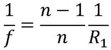
- the imaging law satisfies the following expression:
- R 1 is the radius of curvature of the spherical end of the flat concave air cavity; f is the focal length of the microlens based on the high refractive index medium substrate (starting to calculate from the flat concave air cavity); n is the medium substrate The refractive index; by selecting the R 1 value, the microlens based on the high refractive index medium substrate with the target focal length is obtained.
- the embodiments of the present invention have at least the following beneficial effects: in the above technical solution, by setting a flat concave air cavity in the medium substrate, the plane end of the flat concave air cavity faces the incident surface of the medium substrate, and the spherical surface of the flat concave air cavity The notch at the end faces the exit surface of the medium substrate, and the incident light with a limited wavelength range enters the medium substrate and is focused into a focal point after passing through the flat concave air cavity.
- the full width at half maximum of the focal field strength is smaller than the full width at half maximum defined by the Rayleigh diffraction limit formula size, achieving an Airy disk smaller than the Rayleigh criterion, breaking the existing imaging limit.
- the microlens based on the high refractive index medium substrate of the present invention can be used for optical imaging and detection, and has broad application prospects in the field of micro-nano optics.
- Fig. 1 is a sectional view of an embodiment of the present invention, wherein the hatch line is not drawn;
- Fig. 2 is the optical simulation schematic diagram of the embodiment of the present invention.
- Fig. 3 is a schematic diagram of the electric field intensity of the imaging focus cross-section of the embodiment of the present invention.
- Fig. 4 is the simulation curve of the imaging focus size variation of the embodiment of the present invention and the theoretical Rayleigh criterion diffraction limit
- Fig. 5 is the emulation schematic diagram of the embodiment of the present invention connected with HgCdTe medium
- Fig. 6 is a schematic diagram of the electric field intensity of the imaging focus cross-section after the embodiment of the present invention is connected to the HgCdTe medium;
- Fig. 7 is a schematic diagram of the change of the refractive index of silicon with wavelength based on the environment of 26°C.
- orientation descriptions such as up, down, front, back, left, right, etc. indicated orientations or positional relationships are based on the orientations or positional relationships shown in the drawings, and are only In order to facilitate the description of the present invention and simplify the description, it does not indicate or imply that the device or element referred to must have a specific orientation, be constructed and operated in a specific orientation, and thus should not be construed as limiting the present invention.
- a microlens based on a high refractive index dielectric substrate 101 including a dielectric substrate 101 and a flat surface
- the dielectric substrate 101 is transparent, and the dielectric substrate 101 selected in this embodiment has a high refractive index, specifically, the refractive index of the dielectric substrate 101 is greater than 2.0.
- the dielectric substrate 101 has an incident surface for incident light to enter, and the dielectric substrate 101 has an outgoing surface.
- One end of the flat-concave air cavity 102 is a plane end, and the other end is a notched spherical end.
- the plane end of the flat-concave air cavity 102 faces the incident surface, and the notch of the spherical end of the flat-concave air cavity 102 faces the exit surface, so that the incident light
- the wavelength ⁇ [2.5 ⁇ m-25 ⁇ m] of the incident light can make the full width at half maximum of the focal field strength smaller than the full width at half maximum defined by the Rayleigh diffraction limit formula. More specifically, the wavelength ⁇ [3 ⁇ m ⁇ 5 ⁇ m] of the incident light can make the full width at half maximum of the focal field strength more ideal.
- the dielectric substrate 101 is a cylinder, and the incident surface and the outgoing surface are respectively located on two end surfaces of the cylinder.
- the incident surface of the dielectric substrate 101 is coated with an anti-reflection film, which can increase the amount of incident light.
- the specific number of layers of the anti-reflection film depends on the actual application scene.
- the anti-reflection film includes the first anti-reflection film 201 and the second anti-reflection film. Two antireflection coatings 202 .
- a photodetector is connected to the outgoing surface of the dielectric substrate 101 .
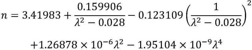
- the material of the dielectric substrate 101 is one of silicon and germanium. Referring to Figure 7, at the wavelength ⁇ [2 .5 ⁇ of incident light
- the refractive index of silicon is greater than 3.41, which is a relatively large value, so silicon can be selected as the base material of the microlens in this wavelength band.
- the dispersion formula of silicon is as follows:
- silicon is used as the material of the dielectric substrate 101.
- silicon has good light transmission and high refractive index.
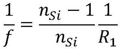
- the specific imaging rule satisfies the following expression:
- R 1 is the radius of curvature of the spherical end of the flat-concave air cavity 102, and the radius of curvature R 1 ⁇ [20 ⁇ m-200 ⁇ m] of the spherical end of the flat-concave air cavity 102;
- f is the focal length of the microlens based on the high refractive index medium substrate 101 (starting to calculate from the plano-concave air cavity 102);
- n si is the refractive index of the dielectric substrate 101
- the microlens based on the high refractive index dielectric substrate 101 with the target focal length can be obtained.
- FIG. 2 is a schematic diagram of optical simulation, wherein the dielectric substrate 101 is silicon, and the incident light is incident on the microlens. At this time,
- the outgoing surface of the dielectric substrate 101 is not connected to the photodetector, specifically the mercury cadmium telluride photodetection component, the wavelength of the incident light is 4 ⁇ m, and the incident light will be focused after passing through the spherical end of the flat-concave air cavity 102 of the microlens, as shown in Fig. 3 is a schematic diagram of the electric field intensity in the cross-section of the imaging focus.
- the full width at half maximum of the focal field strength can be obtained to be smaller than the full width at half maximum defined by the Rayleigh diffraction limit formula.
- the distance from the center of the spherical end of the plano-concave air cavity 102 to the exit surface of the dielectric substrate 101 is defined as L, and L is smaller than the focal length f of the incident light from the spherical end of the plano-concave air cavity 102. It can be understood that , the focal length of the microlens based on the high refractive index dielectric substrate 101 does not fall into the dielectric substrate 101 .
- the outgoing surface of the dielectric substrate 101 is connected to a photodetector, specifically a mercury cadmium telluride photodetector assembly, including components connected to a mercury cadmium telluride medium and a CCD camera.
- the dielectric substrate 101 is made of silicon, and the incident light is incident on the micro Lenses, microlenses based on silicon substrates form a single-lens imaging system that can be used for 3 ⁇ m-5 ⁇ m optical imaging and detection.
- the refractive index of mercury cadmium telluride has a great relationship with its material composition.
- Fig. 5 is a simulated field intensity diagram of a mercury cadmium telluride medium connected to the exit surface
- Fig. 6 is a schematic diagram of the electric field intensity of the imaging focus cross-section after the mercury cadmium telluride medium is connected. The effect does not change much, and the size of the focal spot can still achieve a smaller diffraction limit.
- the CCD camera Through the connected CCD camera, the imaged image can be output to the device.
Landscapes
- Physics & Mathematics (AREA)
- General Physics & Mathematics (AREA)
- Optics & Photonics (AREA)
- Optical Head (AREA)
- Solid State Image Pick-Up Elements (AREA)
- Lenses (AREA)
Abstract
Description
Claims (10)
- 一种基于高折射率介质基底的微透镜,其特征在于:包括透光的介质基底,所述介质基底具有入射面,以供入射光线射入,入射光线的波长λ∈ [2 .5μm‑25μ m],所述介质基底具有出射面;以及平凹空气腔,所述平凹空气腔设置于所述介质基底内,所述平凹空气腔一端为平面端, 另一端为呈凹口的球面端,所述平凹空气腔的平面端朝向所述入射面,所述平凹空气腔的球面端的凹口朝向所述出射面,以使入射光线通过所述平凹空气腔后聚焦成焦点,从而使焦点场强的半高全宽大小小于瑞利衍射极限公式所定义的半高全宽大小。
- 根据权利要求1所述的基于高折射率介质基底的微透镜,其特征在于:入射光线的波长λ∈[3μm‑5μm]。
- 根据权利要求1所述的基于高折射率介质基底的微透镜,其特征在于:所述平凹空气腔的球面端的曲率半径R1∈[20μm‑200μm]。
- 根据权利要求1所述的基于高折射率介质基底的微透镜,其特征在于:所述平凹空气腔的球面端中心到介质基底的出射面的距离定义为L,所述L小于入射光线从所述平凹空气腔的球面端入射的焦距f。
- 根据权利要求1所述的基于高折射率介质基底的微透镜,其特征在于:所述介质基底的入射面镀有增透膜。
- 根据权利要求5所述的基于高折射率介质基底的微透镜,其特征在于:所述介质基底的出射面连接有光电探测器。
- 根据权利要求6所述的基于高折射率介质基底的微透镜,其特征在于:所述介质基底为圆柱体,所述入射面和所述出射面分别位于圆柱体的两个端面。
- 根据权利要求1至7任意一项所述的基于高折射率介质基底的微透镜,其特征在于: 所述介质基底的折射率大于2 .0。
- 根据权利要求8所述的基于高折射率介质基底的微透镜,其特征在于:所述介质基底的材质为硅或锗的其中一种。
- 根据权利要求8所述的基于高折射率介质基底的微透镜,其特征在于,成像规律满足如下的表达式为:
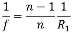 其中, R 1是所述平凹空气腔球面端的曲率半径; f是所述基于高折射率介质基底的微透镜从所述平凹空气腔处开始计算的焦距 ; n是所述介质基底的折射率;通过选取R1值,以获得目标焦距的基于高折射率介质基底的微透镜。
Priority Applications (1)
| Application Number | Priority Date | Filing Date | Title |
|---|---|---|---|
| US18/748,104 US20240337777A1 (en) | 2021-08-20 | 2024-06-20 | Micro-lens based on high-refractive-index dielectric substrate |
Applications Claiming Priority (2)
| Application Number | Priority Date | Filing Date | Title |
|---|---|---|---|
| CN202110960195.4A CN113820763B (zh) | 2021-08-20 | 2021-08-20 | 一种基于高折射率介质基底的微透镜 |
| CN202110960195.4 | 2021-12-21 |
Related Child Applications (1)
| Application Number | Title | Priority Date | Filing Date |
|---|---|---|---|
| US18/748,104 Continuation US20240337777A1 (en) | 2021-08-20 | 2024-06-20 | Micro-lens based on high-refractive-index dielectric substrate |
Publications (1)
| Publication Number | Publication Date |
|---|---|
| WO2023116201A1 true WO2023116201A1 (zh) | 2023-06-29 |
Family
ID=78922940
Family Applications (1)
| Application Number | Title | Priority Date | Filing Date |
|---|---|---|---|
| PCT/CN2022/128464 Ceased WO2023116201A1 (zh) | 2021-08-20 | 2022-10-30 | 一种基于高折射率介质基底的微透镜 |
Country Status (3)
| Country | Link |
|---|---|
| US (1) | US20240337777A1 (zh) |
| CN (1) | CN113820763B (zh) |
| WO (1) | WO2023116201A1 (zh) |
Families Citing this family (2)
| Publication number | Priority date | Publication date | Assignee | Title |
|---|---|---|---|---|
| CN113820763B (zh) * | 2021-08-20 | 2022-10-25 | 华南理工大学 | 一种基于高折射率介质基底的微透镜 |
| CN115755372B (zh) * | 2022-11-12 | 2026-01-30 | 南京师范大学 | 一种应用于超分辨率成像的液体微米透镜 |
Citations (6)
| Publication number | Priority date | Publication date | Assignee | Title |
|---|---|---|---|---|
| US20040108476A1 (en) * | 2002-12-06 | 2004-06-10 | Ultra-Scan Corporation | Method for optimizing performance of optical encoders operating in a fluid |
| US20060088244A1 (en) * | 2004-10-25 | 2006-04-27 | Rpo Pty Limited | Planar lenses for integrated optics |
| CN201084461Y (zh) * | 2007-08-09 | 2008-07-09 | 中国科学院长春光学精密机械与物理研究所 | 一种变焦距x射线组合透镜 |
| CN109713055A (zh) * | 2017-10-20 | 2019-05-03 | 英飞凌科技德累斯顿公司 | 具有无载体的光学干涉滤波器的微透镜 |
| RU2744033C1 (ru) * | 2020-06-01 | 2021-03-02 | Федеральное государственное бюджетное образовательное учреждение высшего образования "Сибирский государственный университет геосистем и технологий" | КВЧ варифокальная линза |
| CN113820763A (zh) * | 2021-08-20 | 2021-12-21 | 华南理工大学 | 一种基于高折射率介质基底的微透镜 |
Family Cites Families (14)
| Publication number | Priority date | Publication date | Assignee | Title |
|---|---|---|---|---|
| US5066114A (en) * | 1990-04-26 | 1991-11-19 | Hodges Marvin P | High refraction index enveloping medium lens system |
| JP3677342B2 (ja) * | 1996-02-23 | 2005-07-27 | 松下電器産業株式会社 | 光ヘッド装置および光ディスク装置 |
| US6785061B2 (en) * | 2002-11-21 | 2004-08-31 | Agilent Technologies, Inc. | Converging air lens structures |
| CN101147088B (zh) * | 2005-02-16 | 2011-08-17 | 应用材料股份有限公司 | 光学耦合至ic芯片 |
| CN100444381C (zh) * | 2006-10-13 | 2008-12-17 | 中国科学院上海技术物理研究所 | 背向集成微透镜红外焦平面探测器及微透镜的制备方法 |
| US8003965B2 (en) * | 2007-05-18 | 2011-08-23 | The Regents Of The University Of Michigan | Apparatus for sub-wavelength near-field focusing of electromagnetic waves |
| CN104089701B (zh) * | 2010-05-07 | 2016-11-09 | 台湾超微光学股份有限公司 | 光学系统 |
| US9529203B2 (en) * | 2012-09-17 | 2016-12-27 | Cytonome/St, Llc | Focal plane shifting system |
| CN103969710B (zh) * | 2014-04-04 | 2016-05-04 | 南京邮电大学 | 一维金属光子晶体柱对称矢量光束聚焦平凹镜 |
| US9829698B2 (en) * | 2015-08-31 | 2017-11-28 | Panasonic Corporation | Endoscope |
| CN108535865A (zh) * | 2018-05-23 | 2018-09-14 | 南京邮电大学 | 一种焦距可控的负折射光栅平凹镜设计方法 |
| US11435037B2 (en) * | 2020-08-31 | 2022-09-06 | Meta Platforms Technologies, Llc | Coupling light source to photonic integrated circuit |
| CN111999786A (zh) * | 2020-09-11 | 2020-11-27 | 电子科技大学 | 一种用不透光膜遮盖球面中心的半球状透镜及其制备方法 |
| CN112099114B (zh) * | 2020-09-29 | 2021-12-21 | 烟台睿创微纳技术股份有限公司 | 一种复合透镜及其制作方法、红外探测器 |
-
2021
- 2021-08-20 CN CN202110960195.4A patent/CN113820763B/zh active Active
-
2022
- 2022-10-30 WO PCT/CN2022/128464 patent/WO2023116201A1/zh not_active Ceased
-
2024
- 2024-06-20 US US18/748,104 patent/US20240337777A1/en active Pending
Patent Citations (6)
| Publication number | Priority date | Publication date | Assignee | Title |
|---|---|---|---|---|
| US20040108476A1 (en) * | 2002-12-06 | 2004-06-10 | Ultra-Scan Corporation | Method for optimizing performance of optical encoders operating in a fluid |
| US20060088244A1 (en) * | 2004-10-25 | 2006-04-27 | Rpo Pty Limited | Planar lenses for integrated optics |
| CN201084461Y (zh) * | 2007-08-09 | 2008-07-09 | 中国科学院长春光学精密机械与物理研究所 | 一种变焦距x射线组合透镜 |
| CN109713055A (zh) * | 2017-10-20 | 2019-05-03 | 英飞凌科技德累斯顿公司 | 具有无载体的光学干涉滤波器的微透镜 |
| RU2744033C1 (ru) * | 2020-06-01 | 2021-03-02 | Федеральное государственное бюджетное образовательное учреждение высшего образования "Сибирский государственный университет геосистем и технологий" | КВЧ варифокальная линза |
| CN113820763A (zh) * | 2021-08-20 | 2021-12-21 | 华南理工大学 | 一种基于高折射率介质基底的微透镜 |
Also Published As
| Publication number | Publication date |
|---|---|
| CN113820763B (zh) | 2022-10-25 |
| US20240337777A1 (en) | 2024-10-10 |
| CN113820763A (zh) | 2021-12-21 |
Similar Documents
| Publication | Publication Date | Title |
|---|---|---|
| JPH07128589A (ja) | 広視野用の結像球面レンズ | |
| CN111474683B (zh) | 一种高数值孔径长波红外显微镜头 | |
| US20240337777A1 (en) | Micro-lens based on high-refractive-index dielectric substrate | |
| CN104216094B (zh) | 一种光学镜头 | |
| CN208953767U (zh) | 一种可见光与近红外共焦的水下成像镜头 | |
| CN110989150A (zh) | 一种大变倍比光学被动半无热化变焦光学系统 | |
| CN111458843B (zh) | 一种中波红外显微镜头 | |
| CN108107559A (zh) | 一种针对不同张角光束的高透光率聚光系统 | |
| TWI857588B (zh) | 光學鏡頭及電子產品 | |
| CN210294661U (zh) | 一种非调焦全折射无热化红外光学系统 | |
| CN104459958A (zh) | 一种用于红外相机的定焦镜头 | |
| CN116299982B (zh) | 一种低温漂激光雷达的长焦接收光学系统 | |
| CN217738457U (zh) | 一种大孔径紧凑型快照式分光成像系统 | |
| TW202141112A (zh) | 五片式紅外線單焦點鏡片組 | |
| TW201723575A (zh) | 四片式紅外單波長鏡片組 | |
| CN201859256U (zh) | 一种长波长焦非制冷无热化红外光学系统 | |
| TW201502570A (zh) | 成像光學裝置 | |
| CN209787287U (zh) | 一种双光变焦拍摄装置 | |
| CN208351112U (zh) | 一种超广角水下微光成像镜头 | |
| RU2629887C1 (ru) | Светосильный трёхлинзовый объектив для ИК-области спектра | |
| CN1828338B (zh) | 透镜 | |
| RU174738U1 (ru) | Инфракрасная зеркально-линзовая система | |
| RU2806167C1 (ru) | Объектив светосильный инфракрасный | |
| CN224137539U (zh) | 光路转换结构、摄像模组和电子设备 | |
| CN223139940U (zh) | 一种宽波段高分辨率低畸变无热化工业镜头 |
Legal Events
| Date | Code | Title | Description |
|---|---|---|---|
| 121 | Ep: the epo has been informed by wipo that ep was designated in this application |
Ref document number: 22909518 Country of ref document: EP Kind code of ref document: A1 |
|
| NENP | Non-entry into the national phase |
Ref country code: DE |
|
| 122 | Ep: pct application non-entry in european phase |
Ref document number: 22909518 Country of ref document: EP Kind code of ref document: A1 |
|
| 122 | Ep: pct application non-entry in european phase |
Ref document number: 22909518 Country of ref document: EP Kind code of ref document: A1 |
|
| 32PN | Ep: public notification in the ep bulletin as address of the adressee cannot be established |
Free format text: NOTING OF LOSS OF RIGHTS PURSUANT TO RULE 112(1) EPC (EPO FORM 1205A DATED 27.05.2025) |
|
| 122 | Ep: pct application non-entry in european phase |
Ref document number: 22909518 Country of ref document: EP Kind code of ref document: A1 |