WO2023105965A1 - 固体撮像素子、及び撮像装置 - Google Patents
固体撮像素子、及び撮像装置 Download PDFInfo
- Publication number
- WO2023105965A1 WO2023105965A1 PCT/JP2022/039734 JP2022039734W WO2023105965A1 WO 2023105965 A1 WO2023105965 A1 WO 2023105965A1 JP 2022039734 W JP2022039734 W JP 2022039734W WO 2023105965 A1 WO2023105965 A1 WO 2023105965A1
- Authority
- WO
- WIPO (PCT)
- Prior art keywords
- imaging device
- solid
- photoelectric conversion
- state imaging
- pixel
- Prior art date
- Legal status (The legal status is an assumption and is not a legal conclusion. Google has not performed a legal analysis and makes no representation as to the accuracy of the status listed.)
- Ceased
Links
Images








Classifications
-
- H—ELECTRICITY
- H04—ELECTRIC COMMUNICATION TECHNIQUE
- H04N—PICTORIAL COMMUNICATION, e.g. TELEVISION
- H04N25/00—Circuitry of solid-state image sensors [SSIS]; Control thereof
- H04N25/40—Extracting pixel data from image sensors by controlling scanning circuits, e.g. by modifying the number of pixels sampled or to be sampled
-
- H—ELECTRICITY
- H04—ELECTRIC COMMUNICATION TECHNIQUE
- H04N—PICTORIAL COMMUNICATION, e.g. TELEVISION
- H04N25/00—Circuitry of solid-state image sensors [SSIS]; Control thereof
- H04N25/70—SSIS architectures; Circuits associated therewith
- H04N25/76—Addressed sensors, e.g. MOS or CMOS sensors
- H04N25/77—Pixel circuitry, e.g. memories, A/D converters, pixel amplifiers, shared circuits or shared components
-
- H—ELECTRICITY
- H10—SEMICONDUCTOR DEVICES; ELECTRIC SOLID-STATE DEVICES NOT OTHERWISE PROVIDED FOR
- H10F—INORGANIC SEMICONDUCTOR DEVICES SENSITIVE TO INFRARED RADIATION, LIGHT, ELECTROMAGNETIC RADIATION OF SHORTER WAVELENGTH OR CORPUSCULAR RADIATION
- H10F39/00—Integrated devices, or assemblies of multiple devices, comprising at least one element covered by group H10F30/00, e.g. radiation detectors comprising photodiode arrays
- H10F39/10—Integrated devices
- H10F39/12—Image sensors
Definitions
- the present disclosure relates to solid-state imaging devices and imaging devices.
- Processing of image data captured by a solid-state image sensor is generally performed by an external device to the solid-state image sensor. If the basic operation of image processing such as convolution operation is performed by the solid-state imaging device of the imaging device, the speed of cooperation with external equipment will be increased, and the user's convenience will be improved.
- the present disclosure provides a solid-state imaging device and an imaging device that are capable of performing arithmetic processing while suppressing an increase in the size of the solid-state imaging device.
- a plurality of pixel regions each composed of a plurality of pixels; a plurality of first charge storage units corresponding to each of the pixel regions;
- a plurality of pixels in the pixel region are a photoelectric conversion unit; a power storage unit corresponding to the photoelectric conversion unit; a first element that establishes a conducting state or a non-conducting state between the photoelectric conversion unit and the electricity storage unit; a second element that brings into a conducting state or a non-conducting state with the electricity storage portion of a pixel that is adjacent to at least one of the vertical direction and the horizontal direction;
- a solid-state imaging device is provided in which at least one of the second elements of the plurality of pixels is connected to the first electricity storage unit.
- the plurality of pixels may be of a front side illumination type or a back side illumination type.
- the accumulation time of the photoelectric conversion unit may be controlled by the first element.
- the pixels are further comprising a third element that establishes a conducting state or a non-conducting state between the photoelectric conversion unit and a predetermined potential line;
- the accumulation time of the photoelectric conversion unit may be controlled by the third element.
- a second power storage unit that accumulates accumulated charges
- a fourth element that establishes a conductive state or a non-conductive state between the first power storage unit and the second power storage unit.
- the number of the second elements in the pixel region may be 2xnHxnV.
- the number of the second elements in the pixel region may be nHxnV+nH or nHxnV+nV.
- the photoelectric conversion element in the pixel region and the second element may be configured in different layers.
- the photoelectric conversion unit may be made of at least one of silicon, indium gallium arsenide, and organic germanium.
- the first and second elements may be composed of at least one of silicon, an oxide semiconductor, and an organic semiconductor.
- the first element may be brought into a conducting state after the photoelectric conversion period of the photoelectric conversion unit is finished.
- the photoelectric conversion period of the photoelectric conversion unit may be controlled according to the weight value of the arithmetic processing.
- the pixel area may be changeable with respect to the corresponding first power storage unit.
- the range of the pixel area with respect to the first power storage unit may be changed according to the calculation range of the calculation process.
- the first power storage unit, the power storage unit, and the second power storage unit may be floating diffusion units.
- An amplifier circuit that amplifies a signal corresponding to the charge accumulated in the first electricity storage unit as a voltage signal may be further provided.
- the amplifier circuit may constitute a source follower circuit, and the voltage signal may be read based on time information of pulse width modulation.
- an analog-to-digital converter that is electrically connected to the fifth element and that converts into digital data corresponding to accumulated electric charges by photoelectric conversion for each pixel region; You may also prepare.
- a solid-state imaging device and an arithmetic processing unit capable of performing a convolution operation
- An imaging apparatus is provided in which the information on the pixel region corresponding to the weight value and the calculation range is supplied from the arithmetic processing unit.
- first digital data generated by an analog-to-digital converter after the photoelectric conversion period of the photoelectric converter is controlled according to the positive weight value of the arithmetic processing and transferred to the first electricity storage unit;
- the photoelectric conversion period of the photoelectric conversion unit is controlled according to the absolute value of the negative weight value of the arithmetic processing, and the second digital signal generated by the analog-to-digital conversion unit after being transferred to the first storage unit You may calculate the difference of data and.
- FIG. 1 is a block diagram showing a configuration example of an imaging device according to an embodiment of the present technology
- FIG. 2 is a block diagram showing a configuration example of a solid-state imaging device
- FIG. 4 is a diagram schematically showing pixels arranged in a matrix in a pixel array section
- FIG. 4 is a diagram showing a configuration example of a reading unit
- FIG. 4 is a diagram showing a configuration example of a pixel array section
- 4A and 4B are diagrams showing configurations of pixels
- FIG. FIG. 2 is a circuit diagram showing a configuration example of a pixel circuit
- FIG. 7 is a plan view of the light receiving chip of the pixel array section shown in FIG.
- FIG. 7 is a plan view of another configuration example of the light-receiving chip of the pixel array section shown in FIG. 6 as viewed from the back side;
- FIG. 4 is a diagram schematically showing a cross section of a main part of a pixel array section;
- FIG. 4 is a diagram showing addition ranges for respective timings and corresponding floating diffusions;
- FIG. 13 is a diagram showing addition ranges at timings different from those in FIG. 12;
- FIG. 14 is a diagram showing addition ranges at timings different from those in FIG. 13 ;
- FIG. 13 is a timing chart showing a processing example of the addition range A11 at timing t1 in FIG. 12;
- FIG. 13 is a timing chart showing another processing example of the addition range at timing t1 in FIG. 12;
- FIG. FIG. 4 is a circuit diagram showing a configuration example of a pixel circuit AFD according to a modification of the first embodiment;
- FIG. 4 is a circuit diagram showing a configuration example of a pixel circuit according to a second embodiment;
- FIG. 20 is a plan view of the pixel array portion shown in FIG. 19;
- FIG. 11 is a diagram showing a configuration example of a pixel array section according to the third embodiment;
- FIG. 22 is a plan view of the pixel array portion shown in FIG. 21;
- FIG. 11 is a diagram showing a configuration example of a pixel array section according to the fourth embodiment;
- FIG. 12 is a diagram showing a configuration example of a pixel according to the fourth embodiment
- FIG. 24 is a plan view of the light-receiving chip of the pixel array section shown in FIG. 23 as viewed from the rear side
- FIG. 11 is a timing chart showing an example of processing according to the fourth embodiment of the addition range
- FIG. The figure which shows typically the example of a process with respect to the weight value of (1) Formula which concerns on 5th Embodiment.
- FIG. 1 is a block diagram showing a configuration example of an imaging device 100 according to an embodiment of the present technology.
- This imaging apparatus 100 includes an imaging lens 110 , a solid-state imaging device 200 , a recording section 120 , a control section 130 , an analysis section 140 , a communication section 150 and a speaker section 160 .
- the imaging device 100 is, for example, a smart phone, a mobile phone, a PC (Personal Computer), or the like.
- the imaging lens 110 collects incident light and guides it to the solid-state imaging device 200 .
- the solid-state imaging device 200 has a plurality of gradation pixels.
- the gradation pixel outputs a luminance signal corresponding to the amount of received light.
- the solid-state imaging device 200 is capable of weighted addition of luminance signals of a plurality of pixels for gradation, for example.
- the pixel for gradation may be called a pixel.
- the solid-state imaging device 200 can perform predetermined signal processing such as weighted addition at the analog signal stage, and outputs the processed data to the recording unit 120 via the signal line 209 .
- the recording unit 120 records data from the solid-state imaging device 200 and the like.
- the control unit 130 controls the imaging device 100 as a whole.
- the control unit 130 controls the solid-state imaging device 200 to capture image data.
- the analysis unit 140 can perform recognition processing using, for example, a neural network.
- the analysis unit 140 has an arithmetic processing unit 142 .
- the arithmetic processing unit 142 can cause the solid-state imaging device 200 to perform arithmetic processing such as convolution on data of each pixel captured by the solid-state imaging device 200 in the analog signal stage.
- the analysis unit 140 can also perform predetermined analysis processing, image processing, etc., using the calculation result of the calculation processing unit 142, for example.
- the arithmetic processing such as the convolution operation performed by the arithmetic processing unit 142 as described above is performed by the solid-state imaging device 200 at the stage of the analog signal, and the subsequent arithmetic processing is performed by the arithmetic processing unit 142 .
- the communication unit 150 performs wireless communication with an external device. Thereby, content or the like is received from an external server and recorded in the recording unit 120 via the control unit 130 .
- the control unit 130 causes the display unit 170 to display an image based on this content, for example.
- the speaker unit 160 has a highly directional speaker and can transmit audio information only to the user.
- the speaker unit 160 can change the direction in which sound is transmitted.
- FIG. 2 is a diagram showing an example of the layered structure of the solid-state imaging device 200 according to the embodiment of the present technology.
- This solid-state imaging device 200 includes a detection chip 202 and a light receiving chip 201 stacked on the detection chip 202 . These substrates are electrically connected through connections such as vias. In addition to vias, Cu--Cu bonding or bumps may be used for connection.
- functions corresponding to the recording unit 120, the control unit 130, and the analysis unit 140 shown in FIG. 1 may be configured in the detection chip 202.
- FIG. In this case, the configuration related to imaging and imaging processing of the imaging device 100 is configured within the layered structure of the solid-state imaging device 200 .
- the light receiving chip 201 and the detection chip 202 may be configured in the same layer.
- FIG. 3 is a block diagram showing a configuration example of the solid-state imaging device 200.
- the solid-state imaging device 200 includes a pixel array section 30, an accumulation control circuit 210, a first access control circuit 211a, a second access control circuit 211b, and a third access control circuit. 211 c , a reading unit 212 , a signal processing unit 213 , a second signal processing unit 214 , a timing control circuit 214 and an output interface 215 .
- the pixel array unit 30 is configured in the light receiving chip 201, and includes an accumulation control circuit 210, a first access control circuit 211a, a second access control circuit 211b, a third access control circuit 211c, a reading unit 212,
- the signal processing section 213 , the second signal processing section 214 , the timing control circuit 214 and the output interface 215 may be configured within the detection chip 202 .
- FIG. 4 is a diagram schematically showing pixels Pix arranged in a matrix in the pixel array section 30.
- a plurality of pixels Pix are two-dimensionally arranged in a matrix (array).
- one floating diffusion FDa is arranged for a processing area Afd corresponding to a predetermined number of pixels Pix.
- a floating diffusion FD is configured for each pixel Pix, and accumulated charges for each floating diffusion FD are integrated by the floating diffusion FDa.
- the pixel array unit 30 has a configuration in which the present technology is applied to a so-called backside illumination type image sensor in which the back side is illuminated with light.
- the present technology may be applied to a front side illuminated image sensor.
- the pixel array section 30 is, for example, a CMOS image sensor.
- the processing area Afd corresponds to the addition range of the floating diffusion FDa described later with reference to FIGS. 11 to 13.
- FIG. This configuration example of the pixel array unit 30 is an example suitable for, for example, a 3 ⁇ 3 weighting filter, but is not limited to this.
- the accumulation control circuit 210 controls the photoelectric conversion units of the pixels Pix. That is, the accumulation control circuit 210 can control resetting of accumulated charges in each of the plurality of photoelectric conversion units, generation of accumulated charges according to weight values, and the like.
- the accumulation control circuit 210 executes a control command according to the weight value of the arithmetic processing section 142 (see FIG. 1) via the control section 130 (see FIG. 1). Details of the photoelectric conversion unit will also be described later.
- the first access control circuit 211a can control the connection of the floating diffusions FD of the plurality of pixels Pix in the row direction, for example, via signal lines HSW1 to HSW3 (see FIG. 6).
- the second access control circuit 211b can control the connection of the floating diffusions FD of the plurality of pixels Pix in the column direction, for example, via signal lines VSW1 to VSW3 (see FIG. 6).
- the third access control circuit 211c cooperates with the first access control circuit 211a and the second access control circuit 211b, resets the accumulated charges of the floating diffusions FD and FDa, charges the floating diffusions FD and FDa, and stores the charges of the floating diffusions FD and FDa. It is possible to control the amplification of the luminance signal according to the accumulated charge of the . Details of control examples of the storage control circuit 210, the first access control circuit 211a, the second access control circuit 211b, and the third access control circuit 211c will also be described later.
- FIG. 5 is a diagram showing a configuration example of the reading unit 212.
- the reading unit 212 has a plurality of constant current sources 220 and a plurality of analog-to-digital conversion units ADC230.
- a plurality of constant current sources 220 and a plurality of AD converters ADC230 are provided corresponding to a plurality of signal lines VSL, respectively.
- the constant current source 21 generates a current corresponding to the accumulated charge of the selected floating diffusion FDa (see FIG. 4) as the image luminance signal Sig for the corresponding signal line VSL.
- the AD conversion unit ADC230 is configured to perform AD conversion based on the signal Sig on the corresponding signal line VSL. That is, the AD conversion unit ADC230 converts the analog gradation luminance signal Sig supplied via the vertical signal line VSL into a digital signal by time division. The AD converter ADC230 supplies the generated digital signal to the signal processor 213 .
- the signal processing section 213 performs predetermined signal processing on the digital signal from the reading section 212 .
- the signal processing unit 213 supplies the data indicating the processing result and the detection signal to the recording unit 120 via the signal line 209 .
- the timing control circuit 214 controls the timing of each component of the solid-state imaging device 200 based on the time stamp information.
- the timing control circuit 212d performs the processes of the accumulation control circuit 210, the first access control circuit 211a, the second access control circuit 211b, the third access control circuit 211c, the reading unit 212, and the signal processing unit 213. Control timing.
- the output interface 215 outputs image data, which is a digital signal supplied from the signal processing unit 213 , to the recording unit 120 .
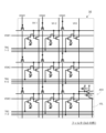
- FIG. 6 is a diagram showing a configuration example of the pixel array section 30. As shown in FIG. For example, it is a configuration example of 3 ⁇ 3 pixels Pix on the upper left with respect to FDa in FIG.
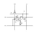
- FIG. 7 is a diagram showing a configuration example of a pixel Pix. As shown in FIG. 7, the pixel Pix has switching elements TR1 to TR3, a photoelectric converter PD, and a floating diffusion FD.
- the photoelectric conversion part PD is an element that generates charges proportional to incident light, and is made of at least one of silicon, indium gallium arsenide, and organic germanium, for example.
- the switching elements TR1 to TR3 are composed of, for example, at least one of silicon, an oxide semiconductor, and an organic semiconductor.
- the accumulation control lines TRG1-9 connect between each pixel Pix and the accumulation control circuit 210 (see FIG. 3). Pulsed control signals Trg1-Trg9 are supplied from the storage control circuit 210 to the storage control lines TRG1-TRG9.
- the horizontal control lines HSW1-HSW3 connect between the pixels Pix in each row and the first access control circuit 211a (see FIG. 3). Pulsed control signals Hsw1-3 are supplied to the horizontal control lines HSW1-HSW3 from the first access control circuit 211a (see FIG. 3).
- the vertical control lines VSW1-3 connect between the pixels Pix in each column and the second access control circuit 211b (see FIG. 3). Pulse-shaped control signals Vsw1-3 are supplied to the vertical control lines VSW1-3 from the second access control circuit 211b.
- the control lines RSTL and RSEL connect between each pixel circuit AFD and the third access control circuit 211c (see FIG. 3).
- the control lines RSTL and RSEL are supplied with pulse-shaped control signals Rst and Sel from the third access control circuit 211c.
- the third access control circuit 211c can perform the reset operation and accumulation operation of the floating diffusions FD and FDa in conjunction with the accumulation control circuit 210, the first access control circuit 211a and the second access control circuit 211b. is.
- the switching elements TR1 to T3 are, for example, N-type MOS (Metal Oxide Semiconductor) transistors.
- the floating diffusion FD is configured using, for example, a diffusion layer formed on the surface of the semiconductor substrate.
- One end of the switching element TR1 is connected to the floating diffusion FD on the left, the other end of the switching element TR1 on the left, and one end of the switching element TR2 on the left.
- the other end of the switching element TR1 is connected to the floating diffusion FD, one end of the switching element TR1 on the right, and one end of the switching element TR2.
- the gate of the switching element TR1 is connected to the horizontal control line HSW.
- the switching element TR1 is in a connected state (on) when the control signals Hsw1-Hsw3 supplied via the horizontal control lines HSW1-3 are high, and is in a non-connected state (off) when the control signals Hsw1-3 are low.
- the connected state (ON) of the switching element may be referred to as the conducting state
- the disconnected state (OFF) may be referred to as the non-conducting state.
- One end of the switching element TR2 is connected to the other end of the upper adjacent switching element TR2, the floating diffusion FD, and one end of the right adjacent switching element TR1.
- the other end of the switching element TR2 is connected to one end of the adjacent switching element TR2 on the lower side.
- the gate of the switching element TR2 is connected to the vertical control line VSW.
- the switching element TR2 is in a connected state (on) when the control signals Vsw1-3 supplied via the horizontal control lines VSW1-3 are high, and is in a non-connected state (off) when the control signals Vsw1-3 are low.
- the switching element TR2 may be referred to as a vertical transfer transistor.
- One end of the switching element TR3 is connected to one end of the photoelectric conversion unit PD, and the other end is connected to the floating diffusion FD. Also, the gate of the switching element TR3 is connected to the storage control line TRG. As a result, the switching element TR3 is in a connected state (on) when the control signal Trg supplied via the storage control line TRG is high, and is in a non-connected state (off) when it is low. Note that the switching element TR3 may be referred to as a TRG transistor. As shown in FIG. 6, when the number of pixels in the addition range (filter range) is nHxnV, the number of switching elements TR1 and TR2 in the addition range is 2xnHxnV.
- nH indicates the number of pixels in the row direction of the filter range
- nV indicates the number of pixels in the vertical direction of the filter range.
- FIG. 8 is a circuit diagram showing a configuration example of the pixel circuit AFD.
- the pixel circuit AFD has a control line RSTL and a control line RSEL.
- One ends of the control lines RSTL and RSEL are connected to the third access control circuit 211c (see FIG. 3) as described above.
- a pulse-shaped control signal Rst is supplied to the control line RSTL by the third access control circuit 211c.
- the control line SELL is supplied with a pulse-shaped control signal Sel by the third access control circuit 211c.
- the pixel circuit AFD has three switching elements RST, AMP, SEL and a floating diffusion FDa.
- the switching elements RST, AMP, and SEL are, for example, N-type MOS (Metal Oxide Semiconductor) transistors.
- the floating diffusion FDa is configured using, for example, a diffusion layer formed on the surface of the semiconductor substrate.
- the switching elements ST, AMP, and SEL are made of, for example, at least one of silicon, an oxide semiconductor, and an organic semiconductor.
- One end of the switching element RST is connected to the floating diffusion FDa, and the other end is connected to the power supply VDD. Also, the gate of the switching element RST is connected to the control line RSTL. As a result, the switching element RST is in a connected state (on) when the control signal Rst supplied via the control line RSTL is high, and is in a non-connected state (off) when it is low. Note that the switching element RST may be referred to as a reset transistor.
- One end of the switching element AMP is connected to the power supply VDD, and the other end is connected to one end of the switching element SEL. Also, the gate of the switching element AMP is connected to the floating diffusion FDa. As a result, the switching element AMP supplies a voltage signal corresponding to the charge accumulated in the floating diffusion FDa to one end of the switching element SEL. Note that the switching element AMP may be referred to as an amplification transistor.
- One end of the switching element SEL is connected to the other end of the switching element AMP, and the other end is connected to the signal line VSL. Also, the gate of the switching element SEL is connected to the control line RSEL. As a result, the switching element SEL is in a connected state (on) when the control signal Rsel supplied via the main line RSEL is high, and is in a non-connected state (off) when it is low. Note that the switching element SEL may be referred to as a route selection transistor.
- the switching element RST is rendered conductive based on the control signal Rst, and similarly, the switching elements TR1 and TR2 are rendered conductive based on the control signals Hsw1-3 and the control signals Vsw1-3. , the floating diffusion FDa, and the floating diffusion FD of each pixel are discharged. Then, the switching element RST becomes non-conductive based on the control signal Rst, and similarly, the switching elements TR1 and TR2 become non-conductive based on the control signals Hsw1-3 and the control signals Vsw1-3.
- the switching elements TR1 and TR2 are brought into conduction based on the control signals Hsw1 to Hsw3 and the control signals Vsw1 to Vsw3. It accumulates charges transferred from the photoelectric conversion unit PD via the floating diffusion FD.
- the pixel circuit AFD is electrically connected to the signal line VSL by turning on the switching element SEL based on the control signal Sel.
- the switching element AMP is connected to the constant current source 220 (see FIG. 5) of the reading section 212 and operates as a so-called source follower.
- a voltage signal corresponding to the voltage of the floating diffusion FDa at that time is output to the ADC 230 as the image luminance signal Sig as described above.
- the switching element AMP constitutes a source follower circuit, and the voltage signal is read based on the time information of pulse width modulation (PWM).
- PWM pulse width modulation
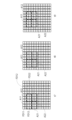
- FIG. 9 is a plan view of the light-receiving chip 201 of the pixel array section 30 shown in FIG. 6 as seen from the rear side.
- the photoelectric conversion units PD of each pixel Pix are arranged in a two-dimensional array.
- Switching elements TR1 to TR3 are arranged around the photoelectric conversion part PD.
- the other end of the switching element TR2 of the lower right pixel Pix in the upper left 3 ⁇ 3 pixel Pix drawing (see FIG. 6), the floating diffusion FDa and the gate of the switching element AMP, and one end of the switching element RST are Connected.
- the floating diffusion FD of each pixel is finally accumulated in the floating diffusion FDa and read out as the image luminance signal Sig.
- FIG. 10 is a plan view of another configuration example when the light receiving chip 201 of the pixel array section 30 shown in FIG. 6 is viewed from the back side.
- the diffusion layer of the floating diffusion FD of three pixels is shared, and the number of floating diffusions FD is suppressed more than the pixel array section 30 of FIG.
- the control lines TRG1-9, HSW1-3, and VSW1-3 are omitted, but the control lines are connected to the gates of the switching elements in the same manner as in FIG.
- FIG. 11 is a diagram schematically showing a cross section of a main part of the pixel array section 30.
- a light receiving chip 201 corresponds to the semiconductor layer 100S
- a detection chip 202 corresponds to the semiconductor layers 100T, 200T and 200S.
- the semiconductor layers 100S and 100T are indicated by the substrate 201a
- the semiconductor layers 200T and 200S are indicated by the substrate 201b.
- the substrates 201a and 201b are electrically connected by, for example, through electrodes 120E and 121E.
- the photoelectric conversion part PD, floating diffusion FD, and VSS contact region 118 have planar regions.
- the photoelectric conversion part PD is composed of, for example, a p-well layer 115 and an n-type semiconductor region 114 .
- the switching element TR3 may be composed of a planar transistor.
- a transfer gate TG is provided on the surface of the semiconductor layer 100S.
- the side surfaces of this transfer gate TG are covered with sidewalls SW.
- the sidewall SW contains silicon nitride (SiN), for example.
- a gate insulating film is provided between the semiconductor layer 100S and the transfer gate TG.
- the transfer gate TG of each pixel Pix is provided, for example, so as to surround the floating diffusion FD in plan view.
- the semiconductor layer 100S is provided with a pixel separation section 117 that separates the pixels ix from each other.
- the pixel separation portion 117 is formed extending in the normal direction of the semiconductor layer 100S (the direction perpendicular to the surface of the semiconductor layer 100S).
- the pixel separation section 117 is provided so as to separate the pixels Pix from each other, and has, for example, a grid-like planar shape (see FIG. 4).
- the pixel separation unit 117 electrically and optically separates the pixels Pix from each other, for example.
- the pixel separation section 117 includes, for example, a light shielding film 117A and an insulating film 117B. For example, tungsten (W) or the like is used for the light shielding film 117A.
- the insulating film 117B is provided between the light shielding film 117A and the p-well layer 115 or the n-type semiconductor region 114. As shown in FIG.
- the insulating film 117B is made of, for example, silicon oxide (SiO).
- the pixel separation section 117 has, for example, an FTI (Full Trench Isolation) structure and penetrates the semiconductor layer 100S. Although not shown, the pixel separation section 117 is not limited to the FTI structure penetrating the semiconductor layer 100S. For example, a DTI (Deep Trench Isolation) structure that does not penetrate the semiconductor layer 100S may be used.
- the pixel separation portion 117 extends in the normal direction of the semiconductor layer 100S and is formed in a partial region of the semiconductor layer 100S.
- a pinning region 116 is provided in the semiconductor layer 100S.
- the pinning region 116 is provided on the side surface of the pixel isolation portion 117 , specifically between the pixel isolation portion 117 and the p-well layer 115 or the n-type semiconductor region 114 .
- the pinning region 116 is composed of, for example, a p-type semiconductor region.
- FIG. 12 to 14 are diagrams exemplifying the range of calculation processing of weighting calculation.
- FIG. 12 is a diagram showing addition ranges A11 to A22 at timings t1 to t3 and corresponding floating diffusions FD11 to FD22.
- FIG. 13 shows the range of addition at timings t4 to t6
- FIG. 14 shows the range of addition at timings t7 to t9.
- 12 to 15 the addition ranges A11 to A22 and the corresponding floating diffusions FDa11 to FDa22 relatively indicate arbitrary regions of the pixel array section 30.
- FIG. 12 to 14 are diagrams exemplifying the range of calculation processing of weighting calculation.
- FIG. 12 is a diagram showing addition ranges A11 to A22 at timings t1 to t3 and corresponding floating diffusions FD11 to FD22.
- FIG. 13 shows the range of addition at timings t4 to t6
- FIG. 14 shows the range of addition at timings t7 to t
- the addition range of the floating diffusion FDa11 is the addition range A11
- the addition range of the floating diffusion FDa12 is the addition range A12
- the addition range of the floating diffusion FDa21 is the addition range A21
- the addition range of the floating diffusion FDa22 is the addition range A22.
- Other floating diffusions FDan similarly have addition ranges An.
- the addition ranges overlap, so nine times of addition processing at timings t1 to t9 are performed within the imaging element 200. FIG. That is, nine images are captured at timings t1 to t9.
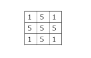
- FIG. 15 is a diagram showing an example of 3 ⁇ 3 weight values w ij in equation (1).
- equation (1) is an example of addition processing used in the processing of the arithmetic processing unit 142 (see FIG. 1).
- the arithmetic processing unit 142 supplies, for example, the weight value wij information of the equation (1) to the accumulation control circuit 210 (see FIG. 3) via the control unit 130 .
- the weight value wij may be referred to as a filter value, and the addition range may be referred to as a filter.
- the image luminance signal Sigij is calculated by adding the weight value wij to the luminance value pij .
- i, j indicate the position of the pixel Pix in the pixel array. That is, i indicates the position in the horizontal direction in the pixel array section 30, and j indicates the position in the vertical direction.
- the luminance value p ij corresponds to the charge accumulated in the photoelectric conversion unit PD in the pixel range Pix at positions i and j.
- the addition range A11 in FIGS. 12 to 14 shows an example of the addition range in which the brightness value p ij of the equation (1) is included in the addition process.
- the charge proportional to the charge accumulated in the 3 ⁇ 3 floating diffusion FD in the addition range A11 is finally accumulated in the floating diffusion FDa11.
- the charge proportional to the charge accumulated in the 3 ⁇ 3 floating diffusion FD in the addition range A12 is finally accumulated in the floating diffusion FDa12.
- the charge proportional to the charge accumulated in the 3 ⁇ 3 floating diffusion FD in the addition range A21 is finally accumulated in the floating diffusion FDa11.
- the charge proportional to the charge accumulated in the 3 ⁇ 3 floating diffusion FD in the addition range A22 is finally accumulated in the floating diffusion FDa22.
- the addition range A11 to A22 shifts to the right by one pixel range
- the addition range A11 to A22 further shifts to the right by one pixel range.
- the addition range A11 to A22 shifts downward by one pixel range from the position at timing t1, and at timing t5, the addition range A11 to A22 further shifts to the right by one pixel.
- the addition range A11 to A22 is further shifted to the right by one pixel range. As shown in FIG.
- the addition range A11 to A22 shifts downward by one pixel range from timing t4, and at timing t5, the addition range A11 to A22 shifts one pixel to the right.
- the addition range A11 to A22 is further shifted to the right by one pixel range. In this manner, in the calculation process of the weighting calculation shown in, for example, formula (1), the addition process is performed while changing the addition range A11 to A22 nine times.
- the accumulation control circuit 210 supplies each pixel Pix with signals Trg1 to TrgH*V having time information proportional to the weight value wij . Then, the photoelectric conversion unit PD of each pixel Pix performs photoelectric conversion based on the signals Trg1 to TrgH*V for a period of time proportional to the weight value wij to accumulate charges. That is, in the present embodiment, a calculation corresponding to the weight value wij is performed by performing photoelectric conversion for a time proportional to the weight value wij . Then, the accumulated charge for each pixel Pix is finally transferred to the floating diffusion FDa.
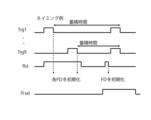
- FIG. 16 is a timing chart showing a processing example of the addition range A11 at timing t1 in FIG. A processing example of the addition range A11 will be described based on FIG. 16 while referring to FIGS.
- the vertical axis indicates Trg1-9, Rst, and Rsel in order from the top.
- the horizontal axis indicates time.
- the switching element RST of the pixel circuit AFD is turned on by the high level signal Rst, and the switching elements TR1 and TR2 are turned on based on the control signals Hsw1-3 and control signals Vsw1-3.
- the ranges of the switching elements TR1 and TR2 connected to the floating diffusion FDa are changed according to the area A11 from timings t1 to t9.
- each switching element TR3 becomes conductive, and the charges in each photoelectric conversion unit PD and each floating diffusion FD and the charges in the floating diffusion FDa are supplied to the power supply VDD. Ejected and initialized. Then, when the control signals Trg1 to Trg9 transition from high level signals to low level signals, each photoelectric conversion unit PD accumulates electric charge according to the amount of received light for an accumulation time proportional to the weight value wij .
- the signal Rst becomes a low level signal and the switching element RST becomes conductive
- the signal Rst becomes a high level signal again.
- the charges in each floating diffusion FD and the charges in the floating diffusion FDa are discharged to the power supply VDD and initialized again.
- the control signals Trg1 to Trg9 become a high level signal
- the charges in each photoelectric conversion unit PD are transferred to each floating diffusion FD, and further transferred to the floating diffusion FDa. . That is, the charge corresponding to the processing result equivalent to the addition processing of formula (1) is transferred into the floating diffusion FDa.
- the switching element SEL becomes conductive, and the signal Sig proportional to the charge accumulated in the floating diffusion FDa is output to the conversion unit ADC 230 of the reading unit 212 (see FIG. 5) via the VSL line. be done.
- the other addition ranges A12 to An are similarly driven at the same time, and charges corresponding to the addition ranges A12 to An are accumulated in each floating diffusion FDa. Then, as described above, each electric charge of the floating diffusion FDa connected to the same VS1 line is sequentially amplified and converted into a digital luminance signal in a time division manner.
- FIG. 17 is a timing chart showing another processing example of the addition range A11 at timing t1 in FIG.
- a processing example of the addition range A11 will be described based on FIG. 16 while referring to FIGS.
- the end points of the light receiving times of the photoelectric conversion units PD are aligned, whereas in the processing example shown in FIG. differ.
- the vertical axis indicates Trg1-9, Rst, and Rsel in order from the top.
- the horizontal axis indicates time.
- the switching element RST of the pixel circuit AFD is turned on by the high level signal Rst, and the switching elements TR1 and TR2 are turned on based on the control signals Hsw1-3 and control signals Vsw1-3.
- the control signals Trg1 to Trg9 become high level signals, the charges in each photoelectric conversion unit PD, each floating diffusion FD, and the charges in the floating diffusion FDa are discharged to the power supply VDD and initialized.
- each photoelectric conversion unit PD accumulates electric charge according to the amount of received light for an accumulation time proportional to the weight value wij .
- the signal Rst becomes a low level signal
- the switching element RST becomes conductive
- the signal Rst becomes a high level signal again
- the charges in each floating diffusion FD and the charges in the floating diffusion FDa are discharged to the power supply VDD and initialized again. be done.
- the signal Rst becomes a low level signal again
- the control signals Trg1 to Trg9 become high level signals according to the accumulation time proportional to the weight value wij
- the time proportional to the weight value wij in each photoelectric conversion unit PD is reached. is transferred into each floating diffusion FD and further transferred into the floating diffusion FDa. That is, the charge corresponding to the processing result equivalent to the addition processing of formula (1) is transferred into the floating diffusion FDa.
- the switching element SEL becomes conductive, and the signal Sig proportional to the charge accumulated in the floating diffusion FDa is output to the conversion unit ADC 230 of the reading unit 212 (see FIG. 5) via the VSL line. be done.
- the other addition ranges A12 to An are similarly driven at the same time, and charges corresponding to the addition ranges A12 to An are accumulated in each floating diffusion FDa. Then, as described above, each electric charge of the floating diffusion FDa connected to the same VS1 line is sequentially amplified and converted into a digital luminance signal in a time division manner.
- the photoelectric conversion unit PD of each pixel Pix can A charge is accumulated by photoelectric conversion.
- a weighting operation for example, equation (1)
- the charge accumulated in the floating diffusion FD of each pixel Pix can be transferred to the floating diffusion FDa, it is possible to change the position of the addition range A11 without providing only one floating diffusion FDa corresponding to the addition range A11. It becomes possible. As a result, even when the luminance value p ij is added with a different weight value w ij during addition processing of the image luminance signal Sigij (i ⁇ n ⁇ i ⁇ i+n, j ⁇ m ⁇ j ⁇ j+m), the floating diffusion FDa It becomes possible to cope without increasing the number. As a result, an increase in the size of the arithmetic element 200 can be suppressed.
- the pixel circuit AFD further includes a floating diffusion FDb, and the capacitance of the floating diffusion of the pixel circuit AFD can be switched. Differs from 100. Differences from the imaging apparatus 100 according to the first embodiment will be described below.
- FIG. 18 is a circuit diagram showing a configuration example of a pixel circuit AFD according to a modification of the first embodiment.
- the pixel circuit AFD further has a floating diffusion FDb, a control line FGL, and a switching element FG.
- One end of the control line FGL is connected to the third access control circuit 211c (see FIG. 3).
- a control signal Fg is supplied to the control line FGL by the third access control circuit 211c.
- the switching element FG is, for example, an N-type MOS (Metal Oxide Semiconductor) transistor.
- One end of the switching element RST is connected to the floating diffusion FDb, and the other end is connected to the power supply VDD.
- One end of the switching element FG is connected to the floating diffusion FDa, and the other end is connected to the floating diffusion FDb.
- the gate of the switching element FG is connected to the control line FGL.
- the switching element FG and the switching element RST are brought into conduction based on the control signals Fg and Rst. Thereby, the charges accumulated in the floating diffusion FD and the floating diffusion FD2 are discharged. Next, based on the control signal Rst, the switching element RST is turned off. As a result, after the exposure period T ends, each switching element TR3 becomes conductive based on the control signal Trg. and store charges transferred via the floating diffusion FD.
- the pixel circuit AFD is electrically connected to the signal line VSL by turning on the switching element SEL based on the control signal Sel.
- the switching element AMP is connected to the constant current source 220 (see FIG. 5) of the reading section 212 and operates as a so-called source follower.
- a voltage corresponding to the voltages of the floating diffusion FDa and the floating diffusion FDb at that time is output to the ADC 230 as the image luminance signal Sig as described above.
- the switching element FG and the switching element RST are brought into conduction based on the control signals Fg and Rst. Thereby, the charges accumulated in the floating diffusion FDa and the floating diffusion FDb are discharged. Next, the switching element FG is turned off based on the control signal Fgt. As a result, after the exposure period T is completed, each switching element TR3 is turned on based on the control signal Trg, and the floating diffusion FDa is switched from each photoelectric conversion unit PD. Accumulates the charges transferred via the element TR3 and the floating diffusion FD. After that, the same processing as described above is performed.
- the pixel circuit AFD further includes the floating diffusion FDb. This makes it possible to switch the capacitance of the floating diffusion in accordance with the amount of light received by the solid-state imaging device 200, and to adjust the imaging sensitivity and the storage charge capacity.
- the imaging device 100 according to the second embodiment differs from the imaging device 100 according to the first embodiment in that the number of switching elements TR1 in the Afd region (see FIG. 4) of the pixel array section 30 is reduced to one row. do. Differences from the imaging apparatus 100 according to the first embodiment will be described below.
- FIG. 19 is a diagram showing a configuration example of the pixel array section 30 according to the second embodiment.
- it is a configuration example of 3 ⁇ 3 pixels Pix on the upper left with respect to FDa in FIG.
- the configuration differs from that of the pixel array section 30 according to the first embodiment in that only three switching elements TR1 are arranged for one row.
- the 3 ⁇ 3 addition range filter range
- the switching elements TR1 are three elements for one row
- the range of the photoelectric conversion unit PD and the floating diffusion FD connected to the floating diffusion FDa11 can be changed, for example, from FIGS.
- the addition range A11 in FIG. 14 can be changed.
- the switching element TR1 when the switching element TR1 is arranged for each pixel Pix, in the example of the addition range of 3 ⁇ 3, the switching element TR2 may be three elements for one column. Also in this case, the range of the photoelectric conversion unit PD and the floating diffusion FD connected to the floating diffusion FDa11 can be changed to, for example, the addition range A11 of FIGS. 12 to 14. FIG. Thus, when the number of pixels in the addition range is nHxnV, the number of switching elements TR1 and TR2 in the addition range is nHxnV+nH or nHxnV+nV.
- nH indicates the number of pixels in the addition range in the row direction
- nV indicates the number of pixels in the addition range in the vertical direction.
- FIG. 20 is a plan view of the pixel array section 30 shown in FIG. 19.
- FIG. 20 the pixel array section 30 according to the second embodiment has a configuration in which the number of switching elements TR1 in the Afd region (see FIG. 4) of the pixel array section 30 is reduced to one row or one column. be.
- the number of switching elements TR1 in the Afd region of the pixel array section 30 is reduced to one row or one column. Accordingly, the size of the pixel array section 30 can be reduced by reducing the number of switching elements TR1 or TR2.
- the imaging device 100 according to the third embodiment is different from the second embodiment in that the pixel array section 30 is configured by a photoelectric conversion layer (PD layer) and a pixel transistor layer (pixel Tr layer) via the connection section C10. It is different from the imaging device 100 according to the form. Differences from the imaging apparatus 100 according to the second embodiment will be described below.
- FIG. 21 is a diagram showing a configuration example of the pixel array section 30 according to the third embodiment.
- the pixel array section 30 according to the third embodiment includes a photoelectric conversion layer (PD layer) and a pixel transistor layer (pixel Tr layer) via a connection section C10.
- the photoelectric conversion layer includes a photoelectric conversion unit PD of each pixel Pix and a switching element TR3.
- the pixel transistor layer includes switching elements TR1 and TR2, switching element SEL. AMP and RST are configured.
- the imaging device 100 reduces the number of switching elements TR1 in the Afd region (see FIG. 4) of the pixel array section 30 to one row or one column, and (PD layer) and a pixel transistor layer (pixel Tr layer). Accordingly, by reducing the number of switching elements TR1 or TR2, the size of the pixel array section 30 can be reduced, and the plane area of the pixel array section 30 can be reduced.
- FIG. 23 is a diagram showing a configuration example of the pixel array section 30 according to the fourth embodiment. For example, it is a configuration example of 3 ⁇ 3 pixels Pix on the upper left with respect to FDa in FIG. In FIG. 23, the wiring of TRG1-9 is omitted.
- FIG. 24 is a diagram showing a configuration example of a pixel Pix according to the fourth embodiment.
- the pixel Pix differs from the pixel Pix according to the first embodiment in that it further includes a switching element TR4.
- One end of the switching element TR4 is connected to the pixel Pix, and the other end is connected to the power supply VDD.
- the gate of the switching element TR4 is connected to the control line OFG.
- the control lines OFG 1 - 9 are connected to the accumulation control circuit 210 .
- the switching element TR4 is connected (ON) when the control signal Ofg supplied from the storage control circuit 210 via the main line OFG is high, and is disconnected (OFF) when it is low.
- the switching element TR4 may be referred to as an OFG transistor.
- the number of switching elements TR1 or TR2 may correspond to one row or one column. That is, in an example of 3 ⁇ 3 addition filters, the number of switching elements TR1 or TR2 may be three.
- FIG. 25 is a plan view of the light-receiving chip 201 of the pixel array section 30 shown in FIG. 23, viewed from the rear side.
- the photoelectric conversion units PD of each pixel Pix are arranged in a two-dimensional array.
- Switching elements TR1 to TR4 are arranged around the photoelectric conversion part PD.
- the other end of the switching element TR2 of the lower right pixel Pix in the upper left 3 ⁇ 3 pixel Pix drawing (see FIG. 6), the floating diffusion FDa and the gate of the switching element AMP, and one end of the switching element RST are Connected.
- the charge of the floating diffusion FD of each pixel Pix is finally accumulated in the floating diffusion FDa and read out as the image luminance signal Sig.
- FIG. 26 is a timing chart showing a processing example of the addition range A11 at timing t1 in FIG. 12 according to the fourth embodiment. As shown in FIG. 26, the vertical axis indicates the control signals Ofg1-9, Trg1-9, Rst and Rsel in order from the top. The horizontal axis indicates time.
- each switching element TR4 becomes conductive, and the electric charge in each photoelectric conversion unit PD is discharged to the power supply VDD and initialized. Then, when the control signals Ofg1 to Ofg9 transition from high level signals to low level signals, each photoelectric conversion unit PD accumulates charges according to the amount of received light for an accumulation time proportional to the weight value wij .
- the signal Rsel becomes a high level signal and the switching element SEL becomes conductive. Subsequently, the switching element RST of the pixel circuit AFD is turned on by the high level signal Rst, and the switching elements TR1 and TR2 are turned on based on the control signals Hsw1-3 and control signals Vsw1-3. As a result, the charges in each floating diffusion FD and the charges in the floating diffusion FDa are discharged to the power supply VDD and initialized.
- the other addition ranges A12 to An are similarly driven at the same time, and charges corresponding to the addition ranges A12 to An are accumulated in each floating diffusion FDa. Then, as described above, each electric charge of the floating diffusion FDa connected to the same VS1 line is sequentially amplified and converted into a digital luminance signal in a time division manner.
- the photoelectric conversion unit PD of each pixel Pix can A charge is accumulated by photoelectric conversion.
- a weighting operation for example, equation (1)
- the charge accumulated in the floating diffusion FD of each pixel Pix can be transferred to the floating diffusion FDa, it is possible to change the position of the addition range A11 without providing only one floating diffusion FDa corresponding to the addition range A11. It becomes possible. As a result, even when the luminance value p ij is added with a different weight value w ij during addition processing of the image luminance signal Sigij (i ⁇ n ⁇ i ⁇ i+n, j ⁇ m ⁇ j ⁇ j+m), the floating diffusion FDa It becomes possible to cope without increasing the number. As a result, an increase in the size of the arithmetic element 200 can be suppressed.
- the image pickup apparatus 100 according to the fifth embodiment differs from the image pickup apparatus 100 according to the first embodiment in that it can be driven when the weight value w ij (F104) in equation (1) has a negative value. do. Differences from the imaging apparatus 100 according to the first embodiment will be described below.
- FIG. 27 is a diagram schematically showing a processing example for the weight value w ijj (F104) of the formula (1) according to the fifth embodiment.
- positive access control circuit 210, first access control circuit 211a, second access control circuit 211b, and third access control circuit 211c control Accumulation of each photoelectric conversion element PD is performed for an accumulation time length corresponding to the weight value wij having a value.
- the charge of each pixel Pix is transferred to the floating diffusion FDa through the floating diffusion FD. After that, it is converted into a first digital signal by the AD conversion unit ADC230 (see FIG. 5) and recorded in the recording unit 120 (see FIG. 1). It is assumed that the accumulation time of the length corresponding to the weight value wij having a negative value is zero.
- the weight value w ij having a negative value is controlled by the accumulation control circuit 210, the first access control circuit 211a, the second access control circuit 211b, and the third access control circuit 211c .
- Accumulation of each photoelectric conversion element PD is performed for an accumulation time length corresponding to the absolute value of (F104). Then, the charge between the photoelectric conversion units PD of each pixel Pix is transferred to the floating diffusion FDa via the floating diffusion FD. After that, it is converted into a second digital signal by the AD conversion section ADC 230 (see FIG. 5) and recorded in the recording section 120 (see FIG. 1). It is assumed that the accumulation time of the length corresponding to the weight value wij having a positive value is zero.
- the arithmetic processing unit 142 calculates the difference between the first digital signal in the first frame F100 and the second digital signal in the second frame F102 recorded in the recording unit 120 (see FIG. 1), generates a digital signal corresponding to the weight value w ij (F104) of .
- the calculation result corresponding to the weight value w ij (F104) of the equation (1) is generated as a numerical value.
- the imaging apparatus 100 performs accumulation in each photoelectric conversion element PD for an accumulation time length corresponding to the weight value wij having a positive value, and obtains the first digital signal. Convert. Subsequently, accumulation is performed in each photoelectric conversion element PD for an accumulation time length corresponding to the absolute value of the weight value wij having a negative value, and is converted into a second digital signal. Subsequently, the arithmetic processing unit 142 subtracts the second digital signal from the first digital signal. This makes it possible to drive arithmetic processing when the weight value w ij (F104) in equation (1) has a negative value.
- This technology can be configured as follows.
- a plurality of pixel regions composed of a plurality of pixels; a plurality of first charge storage units corresponding to each of the pixel regions;
- a plurality of pixels in the pixel region are a photoelectric conversion unit; a power storage unit corresponding to the photoelectric conversion unit; a first element that establishes a conducting state or a non-conducting state between the photoelectric conversion unit and the electricity storage unit; a second element that brings into a conducting state or a non-conducting state with the electricity storage portion of a pixel that is adjacent to at least one of the vertical direction and the horizontal direction;
- a solid-state imaging device wherein at least one of the second elements included in the plurality of pixels is connected to the first electricity storage section.
- the pixels are further comprising a third element that establishes a conducting state or a non-conducting state between the photoelectric conversion unit and a predetermined potential line;
- the solid-state imaging device further comprising:
- the solid-state imaging device according to (1), further comprising an amplifier circuit that amplifies a signal corresponding to the charge accumulated in the first electricity storage unit as a voltage signal.
- first digital data generated by an analog-to-digital converter after the photoelectric conversion period of the photoelectric converter is controlled according to the positive weight value of the arithmetic processing and transferred to the first electricity storage unit;
- the photoelectric conversion period of the photoelectric conversion unit is controlled according to the absolute value of the negative weight value of the arithmetic processing, and the second digital signal generated by the analog-to-digital conversion unit after being transferred to the first storage unit.
- 100 imaging device
- 142 arithmetic processing unit
- 200 image sensor
- 210 Accumulation control circuit
- A11 to A22 addition range (pixel range)
- FG switching element (fourth element)
- FD Floating diffusion (storage unit)
- FDa floating diffusion (first power storage unit)
- PD photoelectric conversion unit
- TR1 switching element (second element)
- TR2 switching element
- TR3 switching element
- TR4 Switching element (third element).
Landscapes
- Engineering & Computer Science (AREA)
- Multimedia (AREA)
- Signal Processing (AREA)
- Solid State Image Pick-Up Elements (AREA)
- Transforming Light Signals Into Electric Signals (AREA)
Priority Applications (1)
| Application Number | Priority Date | Filing Date | Title |
|---|---|---|---|
| JP2023566144A JPWO2023105965A1 (https=) | 2021-12-06 | 2022-10-25 |
Applications Claiming Priority (2)
| Application Number | Priority Date | Filing Date | Title |
|---|---|---|---|
| JP2021-197798 | 2021-12-06 | ||
| JP2021197798 | 2021-12-06 |
Publications (1)
| Publication Number | Publication Date |
|---|---|
| WO2023105965A1 true WO2023105965A1 (ja) | 2023-06-15 |
Family
ID=86730080
Family Applications (1)
| Application Number | Title | Priority Date | Filing Date |
|---|---|---|---|
| PCT/JP2022/039734 Ceased WO2023105965A1 (ja) | 2021-12-06 | 2022-10-25 | 固体撮像素子、及び撮像装置 |
Country Status (2)
| Country | Link |
|---|---|
| JP (1) | JPWO2023105965A1 (https=) |
| WO (1) | WO2023105965A1 (https=) |
Citations (3)
| Publication number | Priority date | Publication date | Assignee | Title |
|---|---|---|---|---|
| JP2016219857A (ja) * | 2015-05-14 | 2016-12-22 | ブリルニクスジャパン株式会社 | 固体撮像装置およびその駆動方法、電子機器 |
| WO2018062303A1 (ja) * | 2016-09-29 | 2018-04-05 | 株式会社ニコン | 撮像素子および電子カメラ |
| JP2021093563A (ja) * | 2019-12-06 | 2021-06-17 | ソニーセミコンダクタソリューションズ株式会社 | 固体撮像素子、制御方法 |
-
2022
- 2022-10-25 WO PCT/JP2022/039734 patent/WO2023105965A1/ja not_active Ceased
- 2022-10-25 JP JP2023566144A patent/JPWO2023105965A1/ja not_active Abandoned
Patent Citations (3)
| Publication number | Priority date | Publication date | Assignee | Title |
|---|---|---|---|---|
| JP2016219857A (ja) * | 2015-05-14 | 2016-12-22 | ブリルニクスジャパン株式会社 | 固体撮像装置およびその駆動方法、電子機器 |
| WO2018062303A1 (ja) * | 2016-09-29 | 2018-04-05 | 株式会社ニコン | 撮像素子および電子カメラ |
| JP2021093563A (ja) * | 2019-12-06 | 2021-06-17 | ソニーセミコンダクタソリューションズ株式会社 | 固体撮像素子、制御方法 |
Also Published As
| Publication number | Publication date |
|---|---|
| JPWO2023105965A1 (https=) | 2023-06-15 |
Similar Documents
| Publication | Publication Date | Title |
|---|---|---|
| US10756129B2 (en) | Image sensors having imaging pixels with ring-shaped gates | |
| US9231011B2 (en) | Stacked-chip imaging systems | |
| US9343500B2 (en) | Solid-state imaging device, driving method thereof, and electronic device | |
| JP6075646B2 (ja) | 固体撮像装置およびその駆動方法、並びに電子機器 | |
| CN101656820B (zh) | 固体摄像装置及其制造方法 | |
| US8754452B2 (en) | Solid-state imaging device, method of manufacturing same, and electronic apparatus | |
| CN207022104U (zh) | 图像传感器像素和成像系统 | |
| US10186535B2 (en) | Image sensors with stacked photodiodes | |
| US8638379B2 (en) | Solid-state image pickup device with shared amplifier nearest pixel corresponding to shortest light wavelength and electronic apparatus using the same | |
| JP7497396B2 (ja) | 撮像素子及び撮像装置 | |
| JP2013084744A (ja) | 固体撮像素子および電子機器 | |
| CN104617118A (zh) | 固态摄像装置、固态摄像装置的制造方法以及电子设备 | |
| WO2022149444A1 (ja) | 固体撮像素子および撮像装置 | |
| WO2023105965A1 (ja) | 固体撮像素子、及び撮像装置 | |
| WO2022067455A1 (en) | Solid state imaging device | |
| WO2023042498A1 (ja) | 固体撮像素子、及び撮像装置 | |
| US12256162B2 (en) | Reference pixel column readout | |
| CN100382328C (zh) | 固态成像装置和电子静止照相机 |
Legal Events
| Date | Code | Title | Description |
|---|---|---|---|
| 121 | Ep: the epo has been informed by wipo that ep was designated in this application |
Ref document number: 22903897 Country of ref document: EP Kind code of ref document: A1 |
|
| ENP | Entry into the national phase |
Ref document number: 2023566144 Country of ref document: JP Kind code of ref document: A |
|
| NENP | Non-entry into the national phase |
Ref country code: DE |
|
| 122 | Ep: pct application non-entry in european phase |
Ref document number: 22903897 Country of ref document: EP Kind code of ref document: A1 |