WO2023100808A1 - Insulation chip and signal transmission device - Google Patents
Insulation chip and signal transmission device Download PDFInfo
- Publication number
- WO2023100808A1 WO2023100808A1 PCT/JP2022/043766 JP2022043766W WO2023100808A1 WO 2023100808 A1 WO2023100808 A1 WO 2023100808A1 JP 2022043766 W JP2022043766 W JP 2022043766W WO 2023100808 A1 WO2023100808 A1 WO 2023100808A1
- Authority
- WO
- WIPO (PCT)
- Prior art keywords
- electrode plate
- side electrode
- chip
- insulating layer
- insulating
- Prior art date
Links
Images


Classifications
-
- H—ELECTRICITY
- H01—ELECTRIC ELEMENTS
- H01L—SEMICONDUCTOR DEVICES NOT COVERED BY CLASS H10
- H01L25/00—Assemblies consisting of a plurality of individual semiconductor or other solid state devices ; Multistep manufacturing processes thereof
-
- H—ELECTRICITY
- H01—ELECTRIC ELEMENTS
- H01L—SEMICONDUCTOR DEVICES NOT COVERED BY CLASS H10
- H01L27/00—Devices consisting of a plurality of semiconductor or other solid-state components formed in or on a common substrate
- H01L27/02—Devices consisting of a plurality of semiconductor or other solid-state components formed in or on a common substrate including semiconductor components specially adapted for rectifying, oscillating, amplifying or switching and having at least one potential-jump barrier or surface barrier; including integrated passive circuit elements with at least one potential-jump barrier or surface barrier
- H01L27/04—Devices consisting of a plurality of semiconductor or other solid-state components formed in or on a common substrate including semiconductor components specially adapted for rectifying, oscillating, amplifying or switching and having at least one potential-jump barrier or surface barrier; including integrated passive circuit elements with at least one potential-jump barrier or surface barrier the substrate being a semiconductor body
Definitions
- the present disclosure relates to insulating tips and signal transmission devices.
- an insulated gate driver that applies a gate voltage to the gate of a switching element such as a transistor is known (see Patent Document 1, for example).
- the gate driver has an insulating element such as a transformer or a capacitor that is used to insulate the primary side circuit and the secondary side circuit.
- a gate driver may be required to have an improved withstand voltage.
- Such a problem is not limited to the gate driver, but can similarly occur in a signal transmission device and an insulation chip that insulates the primary side circuit and the secondary side circuit and transmits a signal.
- An insulating chip that solves the above problems includes an element insulating layer having a front surface and a back surface, and a first capacitor and a second capacitor formed in the element insulating layer, wherein the first capacitor is formed on the element insulating layer.
- the second capacitor has a first surface-side electrode plate and a first back-side electrode plate that face each other in the thickness direction, and the second capacitor has the first surface-side electrode plate when viewed from the thickness direction of the element insulating layer. and a second back electrode plate formed to surround the first back electrode plate when viewed from the thickness direction of the element insulating layer.
- the second front-side electrode plate and the second back-side electrode plate face each other in the thickness direction of the element insulating layer, and the first back-side electrode plate and the second back-side electrode plate are arranged in the element insulating layer; It is electrically connected to the side electrode plate.
- a signal transmission device for solving the above problems is configured to perform at least one of transmission and reception of a signal to and from the first circuit through a first chip including a first circuit, an insulation chip, and the insulation chip.
- a second chip including a second circuit the insulating chip including an element insulating layer having a front surface and a back surface; a first capacitor and a second capacitor formed in the element insulating layer;
- the first capacitor has a first front-side electrode plate and a first back-side electrode plate that are arranged to face each other in the thickness direction of the element insulating layer, and the second capacitor has a structure when viewed from the thickness direction of the element insulating layer.
- a second front electrode plate formed to surround the first front electrode plate and a second front electrode plate formed to surround the first rear electrode plate when viewed from the thickness direction of the element insulating layer.
- a back-side electrode plate wherein the second front-side electrode plate and the second back-side electrode plate are opposed to each other in the thickness direction of the element insulating layer, and the first The backside electrode plate and the second backside electrode plate are electrically connected.
- the insulating chip and the signal transmission device it is possible to improve the withstand voltage.
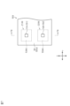
- FIG. 1 is a circuit diagram schematically showing the circuit configuration in one embodiment of the signal transmission device.
- FIG. 2 is a cross-sectional view schematically showing the cross-sectional structure of the signal transmission device of FIG. 3 is a plan view schematically showing a planar structure of an insulating chip in the signal transmission device of FIG. 2.
- FIG. 4 is a cross-sectional view schematically showing the cross-sectional structure of the insulating chip of FIG. 3 taken along a plane perpendicular to its thickness direction.
- FIG. 7 is a plan view schematically showing a planar structure of part of an insulating chip of a comparative example.
- 8 is a cross-sectional view schematically showing the cross-sectional structure of the insulating chip of the comparative example of FIG. 7 taken along line F8-F8.
- FIG. 9 is a cross-sectional view schematically showing the cross-sectional structure of the signal transmission device of the modification.
- FIG. 10 is a plan view schematically showing the planar structure of the insulating chip of the modification.
- FIG. 11 is a plan view schematically showing the planar structure of the insulating chip of the modified example.
- FIG. 12 is a plan view schematically showing the planar structure of the insulating chip of the modification.
- FIG. 13 is a cross-sectional view schematically showing the cross-sectional structure of the insulating chip of the modified example of FIG. 12 taken along a plane perpendicular to the thickness direction thereof.
- FIG. 14 is a cross-sectional view schematically showing the cross-sectional structure of the insulating tip of the modification.
- FIG. 15 is a cross-sectional view schematically showing the cross-sectional structure of the insulating tip of the modification.
- FIG. 1 shows a simplified example of the circuit configuration of the signal transmission device 10. As shown in FIG.
- the signal transmission device 10 is a device that transmits a pulse signal while electrically insulating a primary terminal 11 and a secondary terminal 12 from each other.
- the signal transfer device 10 is a digital isolator, an example of which is an AC/DC converter or gate driver or electronic components contained therein.
- the signal transmission device 10 includes a primary circuit 13 electrically connected to a primary terminal 11, a secondary circuit 14 electrically connected to a secondary terminal 12, and a primary circuit 13.
- a signal transmission circuit 10A having a capacitor 15 electrically connected to the secondary side circuit 14 is provided.
- the primary side circuit 13 corresponds to the "first circuit”
- the secondary side circuit 14 corresponds to the "second circuit”.
- the primary side circuit 13 is a circuit configured to operate when a first voltage is applied.
- the primary circuit 13 is electrically connected, for example, to an external control device (not shown).
- the secondary circuit 14 is a circuit configured to operate when a second voltage different from the first voltage is applied.
- the second voltage is higher than the first voltage, for example.
- the first voltage and the second voltage are DC voltages.
- Secondary circuit 14 is electrically connected to, for example, a drive circuit to be controlled by the control device.
- a drive circuit is a switching circuit.
- the signal transmission device 10 transmits the signal from the primary circuit 13 to the secondary circuit 14 via the capacitor 15 . is transmitted and a signal is output from the secondary side circuit 14 to the drive circuit via the secondary side terminal 12 .
- the signal transmission device 10 transmits a signal from a primary side circuit 13 to a secondary side circuit 14 via a capacitor 15 .
- the primary side circuit 13 and the secondary side circuit 14 are electrically insulated by the capacitor 15 . More specifically, while the capacitor 15 restricts the transmission of the DC voltage between the primary circuit 13 and the secondary circuit 14, it allows the transmission of the pulse signal.
- the state in which the primary side circuit 13 and the secondary side circuit 14 are insulated means the state in which the transmission of the DC voltage is interrupted between the primary side circuit 13 and the secondary side circuit 14. This means that the transmission of the pulse signal from the primary side circuit 13 to the secondary side circuit 14 is permitted.
- the secondary circuit 14 is configured to receive the signal of the primary circuit 13 .
- the dielectric strength of the signal transmission device 10 is, for example, 2500 Vrms or more and 7500 Vrms or less.
- the dielectric breakdown voltage of the signal transmission device 10 of this embodiment is about 5700 Vrms.
- the specific numerical value of the withstand voltage of the signal transmission device 10 is not limited to this and is arbitrary. Further, in this embodiment, as shown in FIG. 1, the ground of the primary circuit 13 and the ground of the secondary circuit 14 are provided independently.
- the signal transmission device 10 of this embodiment includes two capacitors 15 for transmitting two types of signals from the primary circuit 13 to the secondary circuit 14 . More specifically, the signal transmission device 10 includes a capacitor 15 used to transmit a first signal from the primary circuit 13 to the secondary circuit 14 and a second signal from the primary circuit 13 to the secondary circuit 14 . and a capacitor 15 used for transmitting two signals.
- the first signal is a signal containing rise information of the external signal input to the signal transmission device 10
- the second signal is a signal containing fall information of the external signal.
- a pulse signal is generated by the first signal and the second signal.
- the capacitor 15 used for transmitting the first signal is referred to as "capacitor 15A”
- the capacitor 15 used for transmitting the second signal is referred to as "capacitor 15B".
- the signal transmission device 10 includes primary signal lines 16A, 16B and secondary signal lines 17A, 17B.
- the primary signal line 16A is a signal line that connects the primary circuit 13 and the capacitor 15A, and is a signal line that transmits the first signal from the primary circuit 13 to the capacitor 15A.
- the primary side signal line 16B is a signal line that connects the primary side circuit 13 and the capacitor 15B, and is a signal line that transmits the second signal from the primary side circuit 13 to the capacitor 15B.
- the secondary signal line 17A is a signal line that connects the capacitor 15A and the secondary circuit 14, and is a signal line that transmits the first signal from the capacitor 15A to the secondary circuit 14.
- the secondary signal line 17B is a signal line that connects the capacitor 15B and the secondary circuit 14, and is a signal line that transmits the second signal from the capacitor 15B to the secondary circuit 14.
- the first signal is transmitted from the primary circuit 13 to the secondary circuit 14 through the primary signal line 16A, the capacitor 15A, and the secondary signal line 17A in this order.
- the second signal is transmitted from primary circuit 13 to secondary circuit 14 via primary signal line 16B, capacitor 15B, and secondary signal line 17B in this order.
- the capacitor 15A transmits the first signal from the primary circuit 13 to the secondary circuit 14 and electrically insulates the primary circuit 13 and the secondary circuit 14 from each other.
- the capacitor 15A has a first capacitor 21A and a second capacitor 22A connected in series.
- the first capacitor 21A is connected to the primary signal line 16A
- the second capacitor 22A is connected to the secondary signal line 17A.
- the first capacitor 21A and the second capacitor 22A correspond to the "first signal capacitor".
- the first capacitor 21A has a first electrode 23A and a second electrode 24A.
- the first electrode 23A is connected to the primary signal line 16A.
- the second capacitor 22A has a first electrode 25A and a second electrode 26A.
- a second electrode 24A of the first capacitor 21A and a first electrode 25A of the second capacitor 22A are connected to each other by a connection signal line 18A.
- the second electrode 26A is connected to the secondary signal line 17A.
- the capacitor 15B transmits the second signal from the primary circuit 13 to the secondary circuit 14 and electrically insulates the primary circuit 13 and the secondary circuit 14 from each other.
- Capacitor 15B has a first capacitor 21B and a second capacitor 22B that are connected in series with each other.
- the first capacitor 21B is connected to the primary signal line 16B
- the second capacitor 22B is connected to the secondary signal line 17B.
- the first capacitor 21B and the second capacitor 22B correspond to "second signal capacitors".
- the first capacitor 21B has a first electrode 23B and a second electrode 24B.
- the first electrode 23B is connected to the primary signal line 16B.
- the second capacitor 22B has a first electrode 25B and a second electrode 26B.
- a second electrode 24B of the first capacitor 21B and a first electrode 25B of the second capacitor 22B are connected to each other by a connection signal line 18B.
- the second electrode 26B is connected to the secondary signal line 17B.
- the dielectric breakdown voltage of the capacitors 15A and 15B in this embodiment is, for example, 2500 Vrms or more and 7500 Vrms or less.
- the dielectric strength of the capacitors 15A and 15B may be 2500 Vrms or more and 5700 Vrms or less.
- the specific numerical value of the dielectric strength voltage of the capacitors 15A and 15B is not limited to this and is arbitrary.
- FIG. 2 shows an example of a cross-sectional structure schematically showing a part of the internal configuration of the signal transmission device 10.
- the signal transmission device 10 is a semiconductor device in which a plurality of semiconductor chips are packaged.
- the package format of the signal transmission device 10 is, for example, an SO (Small Outline) system, and in this embodiment, it is an SOP (Small Outline Package). Note that the package format of the signal transmission device 10 can be arbitrarily changed.
- the signal transmission device 10 includes a first chip 30, a second chip 40, and an insulating chip 50 as a plurality of semiconductor chips.
- the signal transmission device 10 also includes a primary die pad 60 on which the first chip 30 is mounted, a secondary die pad 70 on which the second chip 40 is mounted, the die pads 60 and 70 and the chips 30, 40, . and a sealing resin 80 that seals 50 .
- the primary die pad 60 corresponds to the "first mounting frame”
- the secondary die pad 70 corresponds to the "mounting frame” or the "second mounting frame”.
- the sealing resin 80 is made of an electrically insulating resin material, such as a black epoxy resin.
- the sealing resin 80 is formed in a rectangular plate shape having a thickness direction in the z direction.
- each die pad 60, 70 is made of a material containing Cu (copper).
- the die pads 60 and 70 may be made of other metal material such as Al (aluminum).
- the material forming each die pad 60, 70 is not limited to a conductive material.
- each die pad 60, 70 may be made of ceramics such as alumina. That is, each of the die pads 60 and 70 may be made of an electrically insulating material. The die pads 60 and 70 are not exposed from the sealing resin 80 in this embodiment.
- the primary die pad 60 and the secondary die pad 70 When viewed from the z-direction, the primary die pad 60 and the secondary die pad 70 are arranged side by side while being separated from each other.
- the arrangement direction of the primary die pads 60 and the secondary die pads 70 when viewed from the z direction is defined as the x direction.
- a direction perpendicular to the x direction when viewed from the z direction is the y direction.
- Both the primary die pad 60 and the secondary die pad 70 are formed in a flat plate shape.
- the x-direction length of the secondary die pad 70 is longer than the x-direction length of the primary die pad 60 .
- the insulating chip 50 is mounted on the secondary die pad 70 . That is, both the insulating chip 50 and the second chip 40 are mounted on the secondary die pad 70 .
- the second chip 40 and the insulating chip 50 are arranged apart from each other in the x direction. Therefore, the chips 30, 40, 50 are arranged apart from each other in the x-direction.
- the chips 30, 40, 50 are arranged in the order of the first chip 30, the insulating chip 50, and the second chip 40 from the primary die pad 60 toward the secondary die pad 70 in the x direction. ing. That is, the insulating chip 50 is arranged between the first chip 30 and the second chip 40 in the x direction.
- the distance between the primary die pad 60 and the secondary die pad 70 is greater than the distance between the second chip 40 and the insulating chip 50 in the x direction when viewed in the z direction. Therefore, when viewed from the z direction, the distance between the first tip 30 and the insulating tip 50 in the x direction is greater than the distance between the second tip 40 and the insulating tip 50 in the x direction. In other words, the insulating chip 50 is arranged closer to the second chip 40 than to the first chip 30 .
- the first chip 30 has a first substrate 33 on which the primary circuit 13 is formed.
- the first substrate 33 is, for example, a semiconductor substrate.
- An example of a semiconductor substrate is a substrate made of a material containing Si (silicon).
- a wiring layer 34 is formed on the first substrate 33 .
- the wiring layer 34 includes a plurality of insulating films stacked in the z-direction, metal layers provided between insulating films adjacent in the z-direction, and vias connecting metal layers positioned at different positions in the z-direction. have.
- the metal layers and vias constitute the wiring pattern of the first chip 30 .
- the metal layers and vias are electrically connected to, for example, primary circuit 13 .
- a protective film 35 is formed on the wiring layer 34 to protect the wiring layer 34 .
- the protective film 35 is made of an electrically insulating material.
- the first chip 30 has a chip front surface 30s and a chip rear surface 30r facing opposite sides in the z direction.
- the first substrate 33 constitutes the chip rear surface 30r
- the protective film 35 constitutes the chip front surface 30s.
- the chip back surface 30 r faces the primary die pad 60 .
- a plurality of first electrode pads 31 and a plurality of second electrode pads 32 are provided in a portion of the first chip 30 near the chip surface 30s. More specifically, each electrode pad 31, 32 is provided so as to be exposed from the chip surface 30s.
- a protective film 35 covers the electrode pads 31 and 32 .
- the protection film 35 has openings that expose the electrode pads 31 and 32 .
- Each of the electrode pads 31 and 32 is electrically connected to the primary circuit 13 by a wiring layer 34, for example.
- a plurality of first electrode pads 31 and a plurality of second electrode pads 32 are formed on the surface of the wiring layer 34 .
- the surface of the wiring layer 34 is the surface of the wiring layer 34 facing the same side as the chip surface 30s.
- the plurality of first electrode pads 31 are arranged on the opposite side of the chip surface 30s from the insulating chip 50 with respect to the center of the chip surface 30s in the x-direction.
- the plurality of electrode pads 31 are arranged apart from each other in the y direction.
- the plurality of second electrode pads 32 are arranged closer to the insulating chip 50 with respect to the center of the chip surface 30s in the x direction in the chip surface 30s.
- the plurality of second electrode pads 32 are arranged apart from each other in the y direction.
- the first chip 30 is bonded to the primary die pad 60 with the first bonding material 101.
- the first bonding material 101 is interposed between the chip back surface 30 r of the first chip 30 and the primary die pad 60 .
- the first bonding material 101 is a conductive bonding material such as solder paste or Ag (silver) paste.
- the primary circuit 13 is electrically connected to the primary die pad 60 via the first bonding material 101 .
- the primary die pad 60 constitutes a ground. Therefore, it can be said that the primary side circuit 13 is electrically connected to the ground.
- the material of the first bonding material 101 can be arbitrarily changed, and may be an insulating bonding material, for example.
- the primary side circuit 13 may be electrically connected to the primary side die pad 60 by a structure other than the first bonding material 101 (for example, a wire).
- the second chip 40 has a second substrate 43 on which the secondary circuit 14 is formed.
- the second substrate 43 is, for example, a semiconductor substrate.
- An example of a semiconductor substrate is a substrate made of a material containing Si.
- a wiring layer 44 is formed on the second substrate 43 .
- the wiring layer 44 includes insulating films stacked in the z-direction, metal layers provided between insulating films adjacent in the z-direction, and vias connecting metal layers positioned at different positions in the z-direction. ing.
- the metal layers and vias constitute the wiring pattern of the second chip 40 .
- the metal layers and vias are electrically connected to, for example, the secondary circuit 14 .
- a protective film 45 is formed on the wiring layer 44 to protect the wiring layer 44 .
- the protective film 45 is made of an electrically insulating material.
- the second chip 40 has a chip front surface 40s and a chip rear surface 40r facing opposite sides in the z direction.
- the second substrate 43 constitutes the chip rear surface 40r
- the protective film 45 constitutes the chip front surface 40s.
- the chip rear surface 40 r faces the secondary die pad 70 .
- the chip rear surface 40 r faces the same side as the chip rear surface 30 r of the first chip 30
- the chip front surface 40 s faces the same side as the chip front surface 30 s of the first chip 30 .
- a plurality of first electrode pads 41 and a plurality of second electrode pads 42 are provided in a portion of the second chip 40 near the chip surface 40s. More specifically, each electrode pad 41, 42 is provided so as to be exposed from the chip surface 40s.
- a protective film 45 covers the electrode pads 41 and 42 .
- the protective film 45 has openings that expose the electrode pads 41 and 42 .
- Each electrode pad 41 , 42 is electrically connected to the secondary circuit 14 by a wiring layer 44 , for example.
- a plurality of first electrode pads 41 and a plurality of second electrode pads 42 are formed on the surface of wiring layer 44 .
- the surface of the wiring layer 44 is the surface of the wiring layer 44 facing the same side as the chip surface 40s.
- the plurality of first electrode pads 41 are arranged closer to the insulating chip 50 with respect to the center of the chip surface 40s in the x direction than the chip surface 40s when viewed from the z direction. Although not shown, the plurality of first electrode pads 41 are arranged apart from each other in the y direction.
- the plurality of second electrode pads 42 are arranged on the opposite side of the chip surface 40s from the insulating chip 50 with respect to the center of the chip surface 40s in the x direction. Although not shown, the plurality of second electrode pads 42 are arranged apart from each other in the y direction.
- the second chip 40 is bonded to the secondary die pad 70 with the second bonding material 102 . More specifically, the second bonding material 102 is interposed between the chip rear surface 40 r and the secondary die pad 70 . The second bonding material 102 bonds the chip rear surface 40 r and the secondary die pad 70 .
- the second bonding material 102 is a conductive bonding material such as solder paste or Ag paste. In this embodiment, the second bonding material 102 is made of the same material as the first bonding material 101, for example.
- the material of the second bonding material 102 can be arbitrarily changed, and may be a conductive bonding material different from the material of the first bonding material 101, for example. Also, the second bonding material 102 may be an insulating bonding material. In this case, the secondary circuit 14 may be electrically connected to the secondary die pad 70 by means of a structure other than the second bonding material 102 (for example, a wire).
- the insulating chip 50 has capacitors 15A and 15B (see FIG. 1). As shown in FIG. 3, the shape of the insulating tip 50 viewed from the z-direction is a rectangle having short sides and long sides. In the present embodiment, the insulating chip 50 is mounted on the secondary die pad 70 so that the long side extends along the y direction and the short side extends along the x direction when viewed from the z direction.
- the insulating chip 50 has a chip front surface 50s and a chip rear surface 50r facing opposite sides in the z direction.
- the chip rear surface 50r faces the secondary die pad 70 side. That is, the chip rear surface 50r faces the same side as the chip rear surface 40r of the second chip 40, and the chip front surface 50s faces the same side as the chip front surface 40s of the second chip 40.
- the insulating chip 50 includes a plurality of (two in this embodiment) first electrode pads 51 and a plurality of (two in this embodiment) second electrode pads 52 .
- Each of the electrode pads 51 and 52 is provided at a portion closer to the chip surface 50s. More specifically, the electrode pads 51 and 52 are provided so as to be exposed from the chip surface 50s when viewed in the z direction.
- the plurality of first electrode pads 51 are arranged closer to the first chip 30 with respect to the center of the chip surface 50s in the x direction than the chip surface 50s.
- the plurality of second electrode pads 52 are arranged closer to the second chip 40 with respect to the center of the chip surface 50s in the x direction in the chip surface 50s.
- a plurality of wires W are connected to each of the first chip 30, the second chip 40, and the insulating chip 50.
- a wire W electrically connects the first chip 30 and the insulating chip 50
- a wire W electrically connects the second chip 40 and the insulating chip 50 .
- Each wire W is a bonding wire formed by a wire bonding apparatus, and is made of a conductor such as Au (gold), Al, Cu, or the like.
- a plurality of first electrode pads 31 of the first chip 30 are individually connected by a plurality of wires W to a plurality of primary leads (not shown).
- the primary lead is a component that constitutes the primary terminal 11 in FIG. Thereby, the primary side circuit 13 and the primary side terminal 11 are electrically connected.
- the primary side lead is made of the same material as the primary side die pad 60 .
- the primary side lead and primary side die pad 60 may be integrally formed.
- the primary leads are spaced apart from the primary die pad 60 on the side opposite to the secondary die pad 70 .
- the primary lead has a portion protruding outward from the sealing resin 80 .
- a portion of the primary lead that protrudes outward from the sealing resin 80 constitutes an external terminal of the signal transmission device 10 .
- the plurality of second electrode pads 32 of the first chip 30 are individually connected to the plurality of first electrode pads 51 of the insulating chip 50 by a plurality of wires W. Thereby, the primary side circuit 13 and the capacitors 15A and 15B (see FIG. 1) are electrically connected. That is, the wiring layer 34 of the first chip 30, the plurality of second electrode pads 32, the plurality of wires W, and the plurality of first electrode pads 51 respectively constitute the primary side signal lines 16A and 16B (see FIG. 1). are doing.
- the plurality of second electrode pads 52 of the insulating chip 50 are individually connected to the plurality of first electrode pads 41 of the second chip 40 by a plurality of wires W. Thereby, the capacitors 15A and 15B and the secondary circuit 14 are electrically connected. That is, the plurality of second electrode pads 52, the plurality of wires W, the first electrode pads 41 of the second chip 40, and the wiring layer 44 respectively constitute the secondary signal lines 17A and 17B (see FIG. 1). there is
- a plurality of second electrode pads 42 of the second chip 40 are individually connected by a plurality of wires W to a plurality of secondary leads (not shown).
- the secondary lead is a component that constitutes the secondary terminal 12 in FIG. Thereby, the secondary circuit 14 and the secondary terminal 12 are electrically connected.
- the secondary lead is made of the same material as the secondary die pad 70 .
- the secondary lead and secondary die pad 70 may be integrally formed.
- the primary lead, primary die pad 60, secondary lead, and secondary die pad 70 may be integrally formed.
- the secondary leads are spaced apart from the secondary die pad 70 on the side opposite to the primary die pad 60 .
- the secondary lead has a portion that protrudes outward from the sealing resin 80 .
- a portion of the secondary lead protruding outward from the sealing resin 80 constitutes an external terminal of the signal transmission device 10 .
- FIG. 1 A detailed configuration of insulation chip
- FIG. 2 A detailed configuration of the insulating tip 50 will be described with reference to FIGS. 2 to 6.
- FIG. 1 the two first electrode pads 51 are referred to as the first electrode pad 51A and the first electrode pad 51B for convenience, and the two second electrode pads 52 are referred to as the second electrode pad 52A and the second electrode pad for convenience. 52B.
- FIG. 3 is a plan view schematically showing the planar structure of the insulating chip 50.
- FIG. 4 is a cross-sectional view schematically showing the cross-sectional structure of the insulating chip 50 taken along a plane orthogonal to the thickness direction of the insulating chip 50.
- FIG. 5 and 6 are cross-sectional views schematically showing cross-sectional structures taken along the cross-section indicating lines in FIG. 3.
- FIG. 4 to 6 hatching lines of some components are omitted from the viewpoint of visibility of the drawings.
- the direction from the chip rear surface 50r to the chip front surface 50s of the insulating chip 50 is defined as upward, and the direction from the chip front surface 50s to the chip rear surface 50r is defined as downward.
- the insulating chip 50 is obtained by integrating both capacitors 15A and 15B into one chip.
- the insulating chip 50 is a chip dedicated to both the capacitors 15A and 15B, separate from the first chip 30 and the second chip 40 (see FIG. 2 for both).
- Both capacitors 15A and 15B are arranged apart from each other in the y direction. In other words, both capacitors 15A and 15B are arranged apart from each other in the longitudinal direction of the insulating chip 50 when viewed from the z direction.
- the first capacitor 21A has a first front-side electrode plate 53A and a first back-side electrode plate 54A that are arranged facing each other in the z-direction.
- the first front-side electrode plate 53A and the first back-side electrode plate 54A are arranged concentrically.
- the first front electrode plate 53A corresponds to the first electrode 23A (see FIG. 1) of the first capacitor 21A
- the first back electrode plate 54A corresponds to the second electrode 24A (see FIG. 1) of the first capacitor 21A. are doing.
- the shape of the first surface-side electrode plate 53A viewed from the z direction is circular.
- the shape of the first backside electrode plate 54A viewed from the z direction is circular.
- the area of the first front electrode plate 53A viewed from the z direction is equal to the area of the first back electrode plate 54A viewed from the z direction.
- the difference between the area of the first front electrode plate 53A viewed from the z direction and the area of the first back electrode plate 54A viewed from the z direction is, for example, the area of the first front electrode plate 53A viewed from the z direction.
- Within 10% of the area it can be said that the area of the first front electrode plate 53A viewed from the z direction is equal to the area of the first back electrode plate 54A viewed from the z direction.
- the second capacitor 22A has a second front-side electrode plate 55A and a second back-side electrode plate 56A that are arranged facing each other in the z-direction.
- the second front electrode plate 55A and the second back electrode plate 56A are arranged concentrically.
- the second front electrode plate 55A corresponds to the second electrode 26A (see FIG. 1) of the second capacitor 22A
- the second back electrode plate 56A corresponds to the first electrode 25A (see FIG. 1) of the second capacitor 22A. are doing.
- the shape of the second surface-side electrode plate 55A viewed from the z-direction is a closed annular shape.
- the second front electrode plate 55A has an inner diameter larger than the diameter of the first front electrode plate 53A.
- the shape of the second backside electrode plate 56A viewed from the z-direction is a closed annular shape.
- the second backside electrode plate 56A has an inner diameter larger than the diameter of the first backside electrode plate 54A.
- the area of the second front electrode plate 55A viewed from the z direction is equal to the area of the second back electrode plate 56A viewed from the z direction.
- the difference between the area of the second front electrode plate 55A viewed from the z direction and the area of the second back electrode plate 56A viewed from the z direction is, for example, the area of the second front electrode plate 55A viewed from the z direction.
- the area of the second front electrode plate 55A viewed from the z direction is equal to the area of the second back electrode plate 56A viewed from the z direction.
- the second surface-side electrode plate 55A is formed so as to surround the first surface-side electrode plate 53A when viewed from the z direction.
- the second front electrode plate 55A is provided so that its center coincides with the center of the first front electrode plate 53A. That is, the first surface-side electrode plate 53A and the second surface-side electrode plate 55A are arranged concentrically. In other words, the first surface-side electrode plate 53A and the second surface-side electrode plate 55A are formed concentrically.
- the second surface-side electrode plate 55A is provided at a position aligned with the first surface-side electrode plate 53A in the z-direction.
- the second surface-side electrode plate 55A When viewed from the z-direction, the second surface-side electrode plate 55A is arranged with a gap from the first surface-side electrode plate 53A.
- a distance G1 between the first surface-side electrode plate 53A and the second surface-side electrode plate 55A as viewed in the z-direction is constant over the entire circumference of the first surface-side electrode plate 53A.
- the distance G1 is greater than or equal to the distance D1 (see FIG. 5) between the first front electrode plate 53A and the first back electrode plate 54A in the z direction. Since the distance G1 is constant over the entire circumference of the first front electrode plate 53A, it can be said that it is the shortest distance between the first front electrode plate 53A and the second front electrode plate 55A when viewed from the z direction. .
- the distance D1 is the distance between the region of the first front electrode plate 53A facing the first rear electrode plate 54A and the region of the first rear electrode plate 54A facing the first front electrode plate 53A. constant throughout each. Therefore, it can be said that the distance D1 is the shortest distance between the first front-side electrode plate 53A and the first back-side electrode plate 54A. Therefore, the shortest distance between the first front-side electrode plate 53A and the second front-side electrode plate 55A as viewed in the z-direction is the distance between the first front-side electrode plate 53A and the first back-side electrode plate 54A. It can be said that it is more than the shortest distance. In this embodiment, distance G1 is equal to distance D1.
- the second capacitor 22A has an electrode pad portion 55AA electrically connected to the second surface-side electrode plate 55A.
- the electrode pad portion 55AA is formed at a different position from the second surface-side electrode plate 55A.
- the electrode pad portion 55AA is provided closer to the second chip 40 than the second surface-side electrode plate 55A.
- the electrode pad portion 55AA and the second surface-side electrode plate 55A are connected by a connection portion 55AB.
- the second surface-side electrode plate 55A, the electrode pad portion 55AA, and the connection portion 55AB are integrally formed.
- the second surface-side electrode plate 55A, the electrode pad portion 55AA, and the connection portion 55AB are provided at positions aligned with each other in the z direction.
- the electrode pad portion 55AA corresponds to "a region formed at a position different from that of the second surface-side electrode plate and integrally formed with the second surface-side electrode plate".
- the electrode pad portion 55AA is formed at a position separated from the second front electrode plate 55A in the x direction, the first front electrode plate 53A and the second front electrode plate 55A are insulated. It is arranged offset in the x direction with respect to the chip 50 .
- the first front-side electrode plate 53A and the second front-side electrode plate 55A are arranged closer to the first chip 30 with respect to the center of the insulating chip 50 in the x direction.
- the first rear electrode plate 54A and the second rear electrode plate 56A are arranged closer to the first chip 30 with respect to the center of the insulating chip 50 in the x direction.
- the second backside electrode plate 56A is formed so as to surround the first backside electrode plate 54A when viewed from the z direction.
- the second backside electrode plate 56A is provided so that its center coincides with the center of the first backside electrode plate 54A. That is, the first rear electrode plate 54A and the second rear electrode plate 56A are formed concentrically.
- the second backside electrode plate 56A is provided at a position aligned with the first backside electrode plate 54A in the z-direction.
- the second backside electrode plate 56A When viewed from the z-direction, the second backside electrode plate 56A is arranged with a gap from the first backside electrode plate 54A.
- a distance G2 between the first rear electrode plate 54A and the second rear electrode plate 56A as viewed in the z-direction is constant over the entire circumference of the first rear electrode plate 54A.
- the distance G2 is greater than or equal to the distance D3 (see FIG. 5) between the second front electrode plate 55A and the second back electrode plate 56A in the z direction. Since the distance G2 is constant over the entire circumference of the first back electrode plate 54A, it can be said that it is the shortest distance between the first back electrode plate 54A and the second back electrode plate 56A when viewed from the z direction. .
- the distance D3 is the distance between the area of the second front electrode plate 55A that faces the second back electrode plate 56A and the area of the second back electrode plate 56A that faces the second front electrode plate 55A. constant throughout each. Therefore, it can be said that the distance D3 is the shortest distance between the second front electrode plate 55A and the second rear electrode plate 56A. Therefore, the shortest distance between the first back electrode plate 54A and the second back electrode plate 56A when viewed in the z direction is the distance between the second back electrode plate 55A and the second back electrode plate 56A. It can be said that it is more than the shortest distance.
- distance G2 is equal to distance D3.
- distance D3 is equal to distance D1.
- the difference between the distance D3 and the distance D1 is, for example, within 10% of the distance D1, it can be said that the distance D3 is equal to the distance D1.
- the area of the second back electrode plate 56A viewed from the z direction is equal to the area of the first back electrode plate 54A viewed from the z direction.
- the difference between the area of the second back electrode plate 56A viewed from the z direction and the area of the first back electrode plate 54A viewed from the z direction is, for example, the first back electrode plate 54A viewed from the z direction.
- the area of the second rear electrode plate 56A viewed from the z direction is equal to the area of the first rear electrode plate 54A viewed from the z direction.
- the area of the first surface-side electrode plate 53A and the area of the second surface-side electrode plate 55A are equal to each other.
- the area of the first back side electrode plate 54A and the area of the second back side electrode plate 56A are equal to each other.
- Distance D1 and distance D3 are equal to each other. From these, it can be said that the capacitance of the first capacitor 21A and the capacitance of the second capacitor 22A are equal to each other.
- the first back-side electrode plate 54A and the second back-side electrode plate 56A are connected by a connection wiring 56AB.
- the connection wiring 56AB is provided at a position aligned with the back-side electrode plates 54A and 56A in the z-direction. In the present embodiment, the connection wiring 56AB extends along the x-direction from the end of the first backside electrode plate 54A near the second chip 40 (see FIG. 2).
- the connection wiring 56AB can be positioned at any position in the circumferential direction of the first back electrode plate 54A as long as it connects the first back electrode plate 54A and the second back electrode plate 56A. It can also be said that the connection wiring 56AB extends along the radial direction of the first back side electrode plate 54A. In this manner, the first backside electrode plate 54A and the second backside electrode plate 56A are electrically connected within the element insulating layer 58 .
- the first capacitor 21B has a first front-side electrode plate 53B and a first back-side electrode plate 54B that are arranged facing each other in the z-direction.
- the second capacitor 22B has a second front-side electrode plate 55B and a second back-side electrode plate 56B that are opposed to each other in the z-direction.
- the second capacitor 22B has an electrode pad portion 55BA and a connecting portion 55BB.
- the first back-side electrode plate 54B and the second back-side electrode plate 56B are connected by a connection wiring 56BB.
- the capacitor 15B has the same configuration as the capacitor 15A, so detailed description thereof will be omitted.
- the first front-side electrode plates 53A, 53B, the first back-side electrode plates 54A, 54B, the second front-side electrode plates 55A, 55B, and the second back-side electrode plates 56A, 56B contain Al. made of material. Therefore, it can be said that the first electrode pads 51A and 51B and the second electrode pads 52A and 52B are made of a material containing Al.
- the material constituting each electrode plate 53A, 53B, 54A, 54B, 55A, 55B, 56A, 56B can be arbitrarily changed, and for example, a material containing Cu, W, or the like may be used.
- each of the electrode plates 53A, 53B, 54A, 54B, 55A, 55B, 56A, and 56B should be made of a material containing at least one of Cu, Al, and W. Further, each electrode plate 53A, 53B, 54A, 54B, 55A, 55B, 56A, 56B may be made of a material containing Ti.
- the insulating chip 50 has a substrate 57 and an element insulating layer 58 formed on the substrate 57 .
- Substrate 57 is formed of, for example, a semiconductor substrate.
- the substrate 57 is a semiconductor substrate made of a material containing Si.
- the substrate 57 may use a wide bandgap semiconductor or a compound semiconductor as a semiconductor substrate.
- the substrate 57 may be an insulating substrate made of a material containing glass or an insulating substrate made of a material containing ceramics such as alumina.
- a wide bandgap semiconductor is a semiconductor substrate having a bandgap of 2.0 eV or more.
- the wide bandgap semiconductor may be SiC (silicon carbide).
- the compound semiconductor may be a III-V compound semiconductor.
- the compound semiconductor may contain at least one of AlN (aluminum nitride), InN (indium nitride), GaN (gallium nitride), and GaAs (gallium arsenide).
- the substrate 57 has a substrate front surface 57s and a substrate rear surface 57r facing opposite sides in the z-direction.
- a plurality of insulating films 58M are laminated in the z direction on the substrate surface 57s.
- the element insulating layer 58 of this embodiment is composed of a plurality of laminated insulating films 58M. Therefore, the z direction can also be said to be the thickness direction of the element insulating layer 58 . Also, "viewed from the z-direction" includes the meaning of "viewed from the thickness direction of the element insulating layer 58".
- Each insulating film 58M is an interlayer insulating film, for example, and is an oxide film formed of a material containing SiO 2 (silicon oxide).
- the thickness of each insulating film 58M may be, for example, 500 nm or more and 5000 nm or less. In this embodiment, the thickness of each insulating film 58M is, for example, about 2000 nm.
- the element insulating layer 58 has a front surface 58s and a rear surface 58r.
- the front surface 58 s faces the same side as the substrate front surface 57 s of the substrate 57
- the rear surface 58 r faces the same side as the substrate rear surface 57 r of the substrate 57 .
- the surface 58s of the element insulating layer 58 is the surface of the uppermost insulating film 58M among the plurality of insulating films 58M stacked in the z direction.
- the rear surface 58r of the element insulating layer 58 is the rear surface of the lowermost insulating film 58M among the plurality of insulating films 58M stacked in the z direction.
- a rear surface 58 r of the element insulating layer 58 faces a substrate surface 57 s of the substrate 57 . More specifically, the back surface 58 r of the element insulating layer 58 is in contact with the substrate surface 57 s of the substrate 57 .
- the surface 58s of the element insulating layer 58 is provided with first surface-side electrode plates 53A and 53B and second surface-side electrode plates 55A and 55B.
- first front-side electrode plates 53A and 53B and the second front-side electrode plates 55A and 55B are provided on the element insulating layer 58 respectively.
- the insulating chip 50 has a surface protective layer 59 formed on the surface 58s of the element insulating layer 58 .
- the surface protective layer 59 is a protective layer that constitutes the chip surface 50 s of the insulating chip 50 and protects the element insulating layer 58 .
- the surface protective layer 59 has a protective film 59A and a passivation film 59B formed on the protective film 59A.
- Protective film 59A is made of a material containing SiO 2 , for example.
- Passivation film 59B is made of a material containing, for example, SiN.
- the passivation film 59B constitutes the chip surface 50s of the insulating chip 50. As shown in FIG.
- the surface protective layer 59 covers the surface 58s of the element insulating layer 58 and the second surface-side electrode plates 55A and 55B.
- the surface protective layer 59 covers the first surface-side electrode plate 53A while exposing a portion of the surface of the first surface-side electrode plate 53A.
- the electrode pad portions 55AA and 55BA are exposed without being covered with the surface protection layer 59.
- the connection portions 55AB and 55BB are covered with a surface protection layer 59.
- the first front-side electrode plates 53A, 53B and the second front-side electrode plates 55A, 55B are covered with a protective film 59A and a passivation film 59B.
- both the protective film 59A and the passivation film 59B are provided with four openings that expose parts of the surfaces of the first front-side electrode plates 53A and 53B and the electrode pad portions 55AA and 55BA.
- the four openings are a first opening exposing the central region of the first surface-side electrode plate 53A, a second opening exposing the central region of the first surface-side electrode plate 53B, and exposing the electrode pad portion 55AA. and a fourth opening exposing the electrode pad portion 55BA. Therefore, exposed surfaces for connecting the wires W are formed on the first surface side electrode plates 53A, 53B and the electrode pad portions 55AA, 55BA through the respective openings.
- the exposed surfaces of the first surface-side electrode plates 53A and 53B constitute first electrode pads 51A and 51B, and the electrode pad portions 55AA and 55BA constitute second electrode pads 52A and 52B.
- regions other than the central regions of the first front-side electrode plates 53A and 53B are covered with a protective film 59A and a passivation film 59B.
- the second surface-side electrode plates 55A, 55B and the connection portions 55AB, 55BB are covered with a protective film 59A and a passivation film 59B.
- the first rear electrode plates 54A, 54B and the second rear electrode plates 56A, 56B are provided within the element insulating layer 58, respectively.
- the first backside electrode plate 54A is embedded in the element insulating layer 58.
- the first rear electrode plate 54A is provided so as to penetrate the one-layer insulating film 58M in the z-direction.
- a conductive member made of a material containing Al, for example, is embedded in the opening to form the first back side electrode plate 54A.
- One or more insulating films 58M are interposed between the first front-side electrode plate 53A and the first back-side electrode plate 54A in the z-direction. That is, the element insulating layer 58 has a portion (inter-electrode insulating film) sandwiched between the first front-side electrode plate 53A and the first back-side electrode plate 54A in the z direction. In other words, the first front-side electrode plate 53A and the first back-side electrode plate 54A are opposed to each other with the element insulating layer 58 (inter-electrode insulating film) interposed therebetween.
- the first backside electrode plate 54A is insulated from the substrate 57 by the element insulating layer 58 .
- the element insulating layer 58 is also provided between the first rear electrode plate 54A and the substrate 57 .
- the distance D1 between the first front electrode plate 53A and the first rear electrode plate 54A in the z direction is the distance D2 between the first rear electrode plate 54A and the rear surface 58r of the element insulating layer 58 in the z direction. bigger than As a result, the distance D1 can be increased while suppressing the thickness TA of the element insulating layer 58 from increasing.
- the second back side electrode plate 56A is embedded in the element insulating layer 58.
- the second backside electrode plate 56A is also formed by embedding a conductive member in an opening of a single-layer insulating film 58M, like the first backside electrode plate 54A.
- the first rear electrode plate 54A, the second rear electrode plate 56A, and the connection wiring 56AB are integrally formed.
- one insulating film 58M of the element insulating layers 58 is provided with openings corresponding to the first rear-side electrode plate 54A, the second rear-side electrode plate 56A, and the connection wiring 56AB. .
- a conductive member (Al) By embedding a conductive member (Al) in this opening, the first rear electrode plate 54A, the second rear electrode plate 56A, and the connection wiring 56AB are integrally formed.
- One or more insulating films 58M are interposed between the second front electrode plate 55A and the second back electrode plate 56A in the z direction. That is, the element insulating layer 58 has a portion (interelectrode insulating film) sandwiched between the second front electrode plate 55A and the second rear electrode plate 56A in the z direction. In other words, the second front-side electrode plate 55A and the second back-side electrode plate 56A are arranged to face each other with the element insulating layer 58 (inter-electrode insulating film) interposed therebetween.
- the second backside electrode plate 56A is insulated from the substrate 57 by the element insulating layer 58 .
- the element insulating layer 58 is also provided between the second backside electrode plate 56A and the substrate 57 .
- the distance D3 between the second front electrode plate 55A and the second rear electrode plate 56A in the z direction is the distance D4 between the second rear electrode plate 56A and the rear surface 58r of the element insulating layer 58 in the z direction. bigger than As a result, the distance D3 can be increased while suppressing the thickness TA of the element insulating layer 58 from increasing.
- distance D3 is equal to distance D1 and distance D4 is equal to distance D2.
- Both D3 can be arbitrarily changed according to the required dielectric strength of the capacitor 15A.
- the required withstand voltage of the capacitor 15A depends on the distances D1 and D3.
- the distance between the electrodes corresponding to the required dielectric strength of the capacitor 15A is used as the reference distance.
- the ratio of the total distance of the distance D1 and the distance D3 to the reference distance is, for example, 1.0 or more and 2.0 or less. This ratio is preferably 1.6, for example.
- the total distance of the distance D1 and the distance D3 is set larger than the reference distance in consideration of the safety margin. It should be noted that increasing the total distance of the distance D1 and the distance D3 invites a decrease in the capacity of the capacitor 15A. Further, when the total distance of the distance D1 and the distance D3 is increased, the distance to the first front electrode plate 53A, the first rear electrode plate 54A, the second front electrode plate 55A, or the second rear electrode plate 56A is increased. There is concern that the influence of the conductive member outside the insulating chip 50 will increase. If this effect is considered, the chip size of the insulating chip 50 becomes large. Therefore, in order to suppress both a decrease in the capacity of capacitor 15A and an increase in the chip size of insulating chip 50, it is preferable to set the total distance of distance D1 and distance D3 close to the reference distance.
- the insulating chip 50 is mounted on the secondary die pad 70. As shown in FIG. More specifically, the insulating chip 50 is mounted on the secondary die pad 70 via the insulating substrate 90 . It can be said that the insulating substrate 90 is interposed between the insulating chip 50 and the secondary die pad 70 .
- the insulating substrate 90 is bonded to the secondary die pad 70 with a third bonding material 103 .
- the insulating chip 50 is bonded to the insulating substrate 90 with the fourth bonding material 104 .
- Both the third bonding material 103 and the fourth bonding material 104 are, for example, insulating bonding materials.
- the insulating substrate 90 corresponds to the "insulating member”.
- the third bonding material 103 corresponds to the "first insulating bonding material”
- the fourth bonding material 104 corresponds to the "second insulating bonding material”.
- the insulating substrate 90 is formed of an insulating substrate containing alumina or an insulating substrate containing glass. Alternatively, the insulating substrate 90 may be made of a resin material.
- the insulating substrate 90 has a front surface 90s and a rear surface 90r facing opposite sides in the z-direction. The front surface 90s is the surface with which the fourth bonding material 104 is in contact, and the back surface 90r is the surface with which the third bonding material 103 is in contact.
- the thickness TS of the insulating substrate 90 is thicker than the distance D2 between the first back-side electrode plate 54A and the back surface 58r of the element insulating layer 58.
- the thickness TS of the insulating substrate 90 can be defined by the distance between the front surface 90s and the rear surface 90r of the insulating substrate 90 in the z direction.
- the insulating chip 50 is mounted on the secondary die pad 70 via the insulating substrate 90, so that the first back electrode plate 54A (54B) of the capacitor 15A (15B) and the secondary die pad 70 is greater than the distance D1.
- the distance D5 is equal to or greater than the thickness TA of the element insulating layer 58 .
- the distance D5 is greater than the thickness TA of the element insulating layer 58.
- the distance D6 between the second back side electrode plate 56A (56B) of the capacitor 15A (15B) and the secondary side die pad 70 is longer than the distance D3.
- the distance D6 is equal to the distance D5.
- Thickness TS of insulating substrate 90 may be, for example, less than distance D2 (D4) or greater than distance D1 (D3).
- the distances D5 and D6 may be less than the distance D1 (D3) or may be smaller than the thickness TA of the element insulating layer 58 .
- the distance between the secondary die pad 70 and the substrate 57 of the insulating chip 50 in the z direction is , the distance between the secondary die pad 70 and the second substrate 43 of the second chip 40 in the z direction. Also, the distance between the secondary die pad 70 and the substrate 57 of the insulating chip 50 in the z direction is greater than the distance between the primary die pad 60 and the first substrate 33 of the first chip 30 in the z direction.
- Method for manufacturing insulating chip and signal transmission device An outline of an example of a method for manufacturing the insulating chip 50 and an example of a method for manufacturing the signal transmission device 10 of this embodiment will be described. Hereinafter, the case of forming a plurality of insulating chips 50 at the same time will be described.
- the manufacturing method of the insulation chip 50 includes a wafer preparation process, a first insulation layer and capacitor formation process, a second insulation layer formation process, and a singulation process.
- a semiconductor wafer forming the substrate 57 is prepared.
- a semiconductor wafer is made of a material containing Si, for example.
- the semiconductor wafer is large enough to form a plurality of insulating chips 50 .
- an element insulating layer is formed on the semiconductor wafer. More specifically, the element insulating layer is formed by laminating a plurality of insulating films made of a material containing SiO2 . This insulating film is an insulating film forming the insulating film 58M (see FIG. 5). The element insulating layer is formed, for example, over the entire surface of the semiconductor wafer. This element insulating layer is an insulating layer forming the element insulating layer 58 (see FIG. 5).
- the insulating film on which the first back electrode plate 54A (54B) and the second back electrode plate 56A (56B) are formed has the first back electrode plate 54A (54B) and the second back electrode plate 54A (54B).
- An opening corresponding to 56A (56B) is provided.
- the first rear electrode plate 54A (54B) and the second rear electrode plate 56A (56B) are formed.
- a material containing Al, for example, is used as the conductive material.
- the first surface-side electrode plate 53A (53B) and the second surface-side electrode plate 55A (55B) are formed on the surface of the element insulating layer.
- the first surface-side electrode plate 53A (53B) and the second surface-side electrode plate 55A (55B) are made of a material containing Al, for example.
- Other conductive materials such as W, Ti, and Cu may be used as materials for forming the electrode plates 53A (53B), 54A (54B), 55A (55B), and 56A (56B).
- the protective film is an insulating film forming the protective film 59A (see FIG. 5), and is formed over the entire surface of the element insulating layer.
- the protective film is made of a material containing SiO2 , for example.
- a passivation film is formed.
- the passivation film is an oxide film forming the passivation film 59B (see FIG. 5) and is formed over the entire surface of the protective film.
- the passivation film is made of a material containing SiN, for example.
- a part including the center of the first surface-side electrode plate 53A (53B) and the openings of the electrode pad portions 55AA (55BA) of the second surface-side electrode plate 55A (55B) are covered with a protective film and a protective film. It is formed on both sides of the passivation film.
- the portion of the first surface-side electrode plate 53A (53B) exposed from both the protective film and the passivation film forms the first electrode pad 51A (51B), and the electrode pad portion 55AA (55BA) forms the second electrode.
- a pad 52A (52B) is configured.
- a mask or the like is used to separate a portion including the center of the first front-side electrode plate 53A (53B) from the electrode pad portion 55AA of the second front-side electrode plate 55A (55B). (55BA) may be formed to expose each of them.
- the semiconductor wafer on which the element insulating layer is formed is cut into the size of the insulating chip 50 . Thereby, the insulating chip 50 is singulated. Through the above steps, the insulating chip 50 is manufactured.
- the method of manufacturing the signal transmission device 10 includes a frame preparation process, a chip mounting process, a wire forming process, a resin layer forming process, a separating process, and a terminal forming process.
- a frame is prepared for forming the primary side lead, the secondary side lead, the primary side die pad 60, and the secondary side die pad 70 (see FIG. 2 for both).
- the primary side lead, the secondary side lead, the primary side die pad 60 and the secondary side die pad 70 are formed by pressing or etching a single plate frame made of a material containing Cu.
- the primary side lead, the secondary side lead, the primary side die pad 60, and the secondary side die pad 70 are each connected to the frame.
- the first chip 30 is mounted on the primary die pad 60 by die bonding, and both the second chip 40 and the insulating chip 50 are mounted on the secondary die pad 70 .
- the first bonding material 101 is applied to the portion of the primary die pad 60 where the first chip 30 is to be mounted, and the portion of the secondary die pad 70 to be mounted with the second chip 40 is coated with the first bonding material 101 .
- a second bonding material 102 is applied.
- the first bonding material 101 and the second bonding material 102 are conductive bonding materials.
- the first chip 30 is placed on the first bonding material 101 and the second chip 40 is placed on the second bonding material 102 .
- the first bonding material 101 and the second bonding material 102 are solidified. For example, when solder paste is used for both bonding materials 101 and 102, both bonding materials 101 and 102 are solidified by cooling both bonding materials 101 and 102, respectively.
- the third bonding material 103 is applied to the portion of the secondary die pad 70 where the insulating chip 50 is to be mounted.
- the third bonding material 103 is an insulating bonding material.
- the insulating substrate 90 is placed on the third bonding material 103 .
- the fourth bonding material 104 is applied onto the insulating substrate 90 .
- the fourth bonding material 104 is an insulating bonding material.
- the insulating chip 50 is placed on the fourth bonding material 104 .
- both bonding materials 103 and 104 are solidified.
- both bonding materials 103 and 104 are made of a material containing epoxy resin
- both bonding materials 103 and 104 are solidified by mixing the epoxy resin with a curing agent.
- wires W connecting the chips 30, 40 and 50, a plurality of wires W connecting the first chip 30 and the primary leads, and the second chip 40 and the secondary leads are formed.
- a plurality of connecting wires W are formed. These wires W are formed, for example, by a wire bonding apparatus.
- a resin layer is formed to seal the chips 30, 40, 50, the wires W, and the die pads 60, 70.
- the resin layer is a layer that constitutes the sealing resin 80, and is made of, for example, a black epoxy resin.
- the resin layer is formed by transfer molding or compression molding, for example.
- part of the primary lead and part of the secondary lead each protrude from the resin layer.
- the resin layer is cut and the primary lead, secondary lead, primary die pad 60, and secondary die pad 70 are separated from the frame.
- a dicing blade is used to cut both the resin layer and the frame.
- the primary side lead and the secondary side lead are cut from the frame so as to have a portion protruding from the resin layer.
- both the primary side lead and the secondary side lead protruding from the resin layer are bent into a predetermined shape by bending. Through the above steps, the signal transmission device 10 is manufactured.
- FIG. 7 schematically shows a part of the planar structure of the insulating tip 50X of the comparative example
- FIG. 8 schematically shows the cross-sectional structure of the insulating tip 50X of the comparative example.
- FIG. 8 schematically shows cross-sectional structures of the first capacitor 21AX and the second capacitor 22AX.
- the insulating chip 50X of the comparative example differs from the insulating chip 50 of the present embodiment only in the capacitor structure, so common components are denoted by the same reference numerals and descriptions thereof are omitted.
- the insulation chip 50X has a package structure in which the first capacitor 21AX and the second capacitor 22AX are integrated into one chip.
- the first capacitor 21AX has a first front-side electrode plate 53AX and a first back-side electrode plate 54AX
- the second capacitor 22AX has a second front-side electrode plate 55AX and a second back-side electrode plate 55AX. 56AX.
- the first front-side electrode plate 53AX and the first back-side electrode plate 54AX are arranged to face each other in the z-direction, and the second front-side electrode plate 55AX and the second back-side electrode plate 56AX are arranged to face each other in the z-direction.
- the first front electrode plate 53AX and the second front electrode plate 55AX are arranged apart from each other in the x direction, and the first rear electrode plate 54AX and the second rear electrode plate 56AX are arranged apart from each other in the x direction. spaced apart.
- the first rear electrode plate 54AX and the second rear electrode plate 56AX are electrically connected within the element insulating layer 58 .
- each electrode plate 53AX, 54AX, 55AX, 56AX viewed from the z direction is rectangular. Therefore, electric field concentration is likely to occur at the corner portions of the electrode plates 53AX, 54AX, 55AX, and 56AX. Due to electric field concentration at the corner portions of the electrode plates 53AX, 54AX, 55AX, and 56AX, the withstand voltage of the capacitors 21AX and 22AX may be lowered.
- the first front-side electrode plate 53A (53B) and the first back-side electrode plate 54A (54B) are circular when viewed from the z direction.
- the second front electrode plate 55A (55B) and the second back electrode plate 56A (56B) are larger in diameter than the first front electrode plate 53A (53B) and the first back electrode plate 54A (54B). It is circular with an inner diameter.
- a second front-side electrode plate 55A is formed so as to surround the first front-side electrode plate 53A and is provided so as to be concentric with the first front-side electrode plate 53A. It is formed so as to surround the back side electrode plate 54A and is provided so as to be concentric with the first back side electrode plate 54A.
- the electrode plates 53A (53B), 54A (54B), 55A (55B), and 56A (56B) do not have corner portions that cause electric field concentration when viewed from the z direction.
- the distance G1 between the first front-side electrode plate 53A (53B) and the second front-side electrode plate 55A (55B) becomes constant, and the first back-side electrode plate 54A (54B) and the second back-side electrode Since the distance G2 between the plates 56A (56B) is constant, electric field concentration is less likely to occur. Therefore, a decrease in dielectric strength of the insulating chip 50 can be suppressed.
- the insulating chip 50 includes an element insulating layer 58 having a front surface 58s and a back surface 58r, and a first capacitor 21A (21B) and a second capacitor 22A (22B) formed on the element insulating layer 58. .
- the first capacitor 21A (21B) has a first front-side electrode plate 53A (53B) and a first back-side electrode plate 54A (54B) that are opposed to each other in the z direction, which is the thickness direction of the element insulating layer 58. ing.
- the second capacitor 22A (22B) includes a second front-side electrode plate 55A (55B) formed so as to surround the first front-side electrode plate 53A (53B) when viewed in the z-direction, and a first front-side electrode plate 55A (55B) when viewed in the z-direction. and a second back electrode plate 56A (56B) formed to surround the back electrode plate 54A (54B).
- the second front side electrode plate 55A (55B) and the second back side electrode plate 56A (56B) face each other in the z direction.
- the first backside electrode plate 54A (54B) and the second backside electrode plate 56A (56B) are electrically connected.
- the withstand voltage of the insulating chip is improved by increasing the distance between the front-side electrode plate and the back-side electrode plate in the z direction.
- the thickness of the element insulating layer also increases. If the thickness of the element insulating layer is increased, warpage of the semiconductor wafer increases during the manufacturing process of the insulating chip, making it difficult to manufacture the insulating chip.
- the first capacitor 21A (21B) and the second capacitor 22A (22B) are connected in series, and the second capacitor 22A (22B) is connected to the first capacitor 21A (21B). It is arranged in the direction perpendicular to the direction. Therefore, it is possible to improve the withstand voltage of the insulating chip 50 without increasing the thickness TA of the element insulating layer 58 . Therefore, it is possible to improve the dielectric strength of the insulating chip 50 and to easily manufacture the insulating chip 50 .
- the second front electrode plate 55A (55B) is formed so as to surround the first front electrode plate 53A (53B) when viewed from the z direction
- the second rear electrode plate 56A (56B) is formed when viewed from the z direction.
- the front side electrode plates 53A (53B) and 55A ( 55B) and the rear electrode plates 54A (54B) and 56A (56B) in the x direction can be reduced. Therefore, it is possible to reduce the size of the insulating chip 50 in the x direction.
- the shape of the first surface-side electrode plate 53A (53B) viewed from the z-direction is circular.
- the second front-side electrode plate 55A (55B) has an annular shape with an inner diameter larger than the diameter of the first front-side electrode plate 53A (53B).
- the first surface-side electrode plate 53A (53B) and the second surface-side electrode plate 55A (55B) are arranged concentrically.
- the shape of the first back side electrode plate 54A (54B) when viewed in the z direction is circular.
- the second backside electrode plate 56A (56B) has an annular shape with an inner diameter larger than the diameter of the first backside electrode plate 54A (54B).
- the first rear electrode plate 54A (54B) and the second rear electrode plate 56A (56B) are arranged concentrically.
- the distance G1 between the first surface-side electrode plate 53A (53B) and the second surface-side electrode plate 55A (55B) is constant in the circumferential direction of the first surface-side electrode plate 53A (53B).
- the distance G2 between the first back electrode plate 54A (54B) and the second back electrode plate 56A (56B) is constant in the circumferential direction of the first back electrode plate 54A (54B).
- the shortest distance G1 between the first front electrode plate 53A (53B) and the second front electrode plate 55A (55B) is the distance between the first front electrode plate 53A (53B) and the first rear electrode. It is the shortest distance to the plate 54A (54B) and is greater than or equal to the distance D1.
- the withstand voltage between the first front electrode plate 53A (53B) and the second front electrode plate 55A (55B) is equal to that of the first front electrode plate 53A (53B) and the first rear electrode. Since it is equal to or higher than the dielectric strength voltage between the plate 54A (54B), a decrease in the dielectric strength voltage of the insulating chip 50 can be suppressed.
- the insulating chip 50 has a surface protective layer 59 that covers the surface 58s of the element insulating layer 58, the first surface-side electrode plate 53A (53B), and the second surface-side electrode plate 55A (55B).
- the surface protective layer 59 exposes a portion of the first surface-side electrode plate 53A (53B).
- the exposed surface of the first surface-side electrode plate 53A (53B) exposed from the surface protective layer 59 can be formed as the first electrode pad 51A (51B).
- one or more insulating films 58M need to be interposed between the first surface-side electrode plate 53A and the electrode pad. There is As a result, the thickness TA of the device insulating layer 58 is increased.
- the first surface-side electrode plate 53A (53B) also serves as an electrode pad, it is possible to prevent the thickness TA of the element insulating layer 58 from increasing. Further, for example, in the case of a configuration in which an electrode pad is formed at a position separated from the first surface-side electrode plate 53A (53B) in the direction orthogonal to the z-direction, the first surface-side electrode plate 53A (53B) and the electrode pad Since a conductive path is formed between , an inductance is generated due to the conductive path. In this regard, in the present embodiment, since the conductive path is not formed, it is possible to avoid the occurrence of inductance due to the conductive path.
- the signal transmission device 10 is configured to receive signals from the primary circuit 13 via the first chip 30 including the primary circuit 13, the insulating chip 50, and the insulating chip 50. and a second chip 40 including the secondary circuit 14 .
- the insulating chip 50 includes an element insulating layer 58 having a front surface 58s and a back surface 58r, and a first capacitor 21A (21B) and a second capacitor 22A (22B) formed on the element insulating layer 58.
- the first capacitor 21A (21B) has a first front-side electrode plate 53A (53B) and a first back-side electrode plate 54A (54B) that are opposed to each other in the z direction, which is the thickness direction of the element insulating layer 58. ing.
- the second capacitor 22A (22B) includes a second front-side electrode plate 55A (55B) formed so as to surround the first front-side electrode plate 53A (53B) when viewed in the z-direction, and a first front-side electrode plate 55A (55B) when viewed in the z-direction. and a second back electrode plate 56A (56B) formed to surround the back electrode plate 54A (54B).
- the second front side electrode plate 55A (55B) and the second back side electrode plate 56A (56B) face each other in the z direction.
- the first backside electrode plate 54A (54B) and the second backside electrode plate 56A (56B) are electrically connected.
- the same effect as the effect (1) above can be obtained.
- the dielectric strength of the insulating chip 50 can be improved, the dielectric strength of the signal transmission device 10 can be improved.
- An insulating substrate 90 is interposed between the insulating chip 50 and the secondary die pad 70 .
- the distances D5 and D6 between the first rear electrode plate 54A (54B) and the second rear electrode plate 56A (56B) and the secondary die pad 70 in the z direction can be increased. . Therefore, it is possible to improve the withstand voltage between the first back side electrode plate 54A (54B) and the second back side electrode plate 56A (56B) and the secondary side die pad .
- the insulating substrate 90 is bonded to the secondary die pad 70 with the third bonding material 103 .
- An insulating bonding material is used for the third bonding material 103 . According to this configuration, the dielectric breakdown voltage between the first capacitor 21A (21B) and the second capacitor 22A (22B) and the secondary die pad 70 can be improved.
- the insulating substrate 90 is formed of an insulating substrate containing alumina or an insulating substrate containing glass. According to this configuration, the insulating substrate 90 having a large thickness can be easily formed as compared with the case where the insulating substrate 90 is made of an insulating film.
- substrate 57 can be changed arbitrarily.
- an SOI substrate may be used as the substrate 57 .
- One of the protective film 59A and the passivation film 59B may be omitted from the surface protective layer 59 .
- the surface protective layer 59 may be omitted.
- each front side electrode plate 53A, 53B, 55A, 55B and each thickness of each back side electrode plate 54A, 54B, 56A, 56B can be changed arbitrarily. In one example, the thickness of each of the front electrode plates 53A, 53B, 55A, 55B may be thicker than the thickness of each of the back electrode plates 54A, 54B, 56A, 56B.
- the second surface-side electrode plates 55A, 55B and the second electrode pads 52A, 52B may be formed separately.
- the insulating chip 50 may have second electrode pads 52A and 52B electrically connected to the second front electrode plates 55A and 55B.
- the second electrode pads 52A and 52B are formed at positions separated from the second surface-side electrode plates 55A and 55B when viewed in the z direction.
- the surface protection layer 59 exposes the surfaces of the second electrode pads 52A and 52B.
- the second surface-side electrode plates 55A, 55B and the second electrode pads 52A, 52B may be connected by wires, for example. Further, in this case, the second electrode pads 52A, 52B may be made of a material different from that of the second front-side electrode plates 55A, 55B.
- both the first surface-side electrode plates 53A, 53B and the second surface-side electrode plates 55A, 55B are formed on the surface 58s of the element insulating layer 58, but this is not the only option.
- the first surface-side electrode plates 53A and 53B may be embedded in the element insulating layer 58.
- first electrode pads 51A and 51B are provided separately from the first front-side electrode plates 53A and 53B on the surface 58s of the element insulating layer 58 above the first front-side electrode plates 53A and 53B. there is The first surface-side electrode plate 53A and the first electrode pads 51A are connected by connection vias.
- the first surface-side electrode plate 53B and the first electrode pads 51B are connected by connection vias.
- the second front-side electrode plates 55A and 55B may be embedded in the element insulating layer 58 .
- second electrode pads 52A and 52B are provided separately from the second front electrode plates 55A and 55B on the surface 58s of the element insulating layer 58 above the second front electrode plates 55A and 55B.
- the second surface-side electrode plate 55A and the second electrode pads 52A are connected by connection vias.
- the second surface-side electrode plate 55B and the second electrode pads 52B are connected by connection vias.
- the first electrode pads 51A, 51B and the second electrode pads 52A, 52B are made of a material containing Al like the first front electrode plates 53A, 53B and the second front electrode plates 55A, 55B.
- the materials forming the first electrode pads 51A, 51B and the second electrode pads 52A, 52B can be changed arbitrarily.
- the first electrode pads 51A, 51B may be made of a material different from that of the first surface-side electrode plates 53A, 53B.
- the second electrode pads 52A, 52B may be made of a material different from that of the second surface-side electrode plates 55A, 55B.
- the area of the first front electrode plate 53A and the area of the second front electrode plate 55A are equal to each other, and the area of the first rear electrode plate 54A and the area of the second rear electrode plate 56A are equal to each other. were equal to each other, but are not limited to this.
- the area of the first front-side electrode plate 53A may be larger than the area of the second front-side electrode plate 55A, and the area of the first back-side electrode plate 54A may be larger than the area of the second back-side electrode plate 56A. That is, the capacity of the first capacitor 21A may be larger than the capacity of the second capacitor 22A.
- the area of the second front electrode plate 55A may be larger than the area of the first front electrode plate 53A, and the area of the second rear electrode plate 56A may be larger than the area of the first rear electrode plate 54A. . That is, the capacity of the second capacitor 22A may be larger than the capacity of the first capacitor 21A.
- the first front-side electrode plate 53B, the first back-side electrode plate 54B, the second front-side electrode plate 55B, and the second back-side electrode plate 56B may also be changed in the same manner.
- the insulating chip 50 may be mounted on the primary die pad 60 instead of the secondary die pad 70 .
- both the first chip 30 and the insulating chip 50 are mounted on the primary die pad 60 .
- the mounting structure of the insulating chip 50 to the primary side die pad 60 is the same as the mounting structure of the insulating chip 50 to the secondary side die pad 70 of the above embodiment.
- the insulating chip 50 may be mounted on an intermediate die pad 110 different from the primary die pad 60 and the secondary die pad 70 .
- Intermediate die pad 110 is electrically floating with respect to primary die pad 60 and secondary die pad 70 .
- the insulating chip 50 is mounted on the mounting frame (intermediate die pad 110) in an electrically floating state.
- the intermediate die pad 110 corresponds to the "mounting frame” and the "third mounting frame”.
- the intermediate die pad 110 may be formed simultaneously with the die pads 60 and 70 from the same material as the die pads 60 and 70, for example. Note that the material forming the intermediate die pad 110 can be arbitrarily changed, and may be formed of a material different from that of the die pads 60 and 70, for example. In one example, the intermediate die pad 110 may be made of an insulating material such as ceramics such as alumina or glass. Also, the intermediate die pad 110 may be made of a resin material.
- the insulating substrate 90 is bonded to the intermediate die pad 110 by the third bonding material 103.
- the insulating chip 50 is bonded to the insulating substrate 90 with the fourth bonding material 104 .
- the third bonding material 103 and the fourth bonding material 104 may be conductive bonding materials.
- a semiconductor substrate may be used instead of the insulating substrate 90 interposed between the intermediate die pad 110 and the insulating chip 50 .
- the insulating substrate 90 may be omitted. That is, the insulating chip 50 may be bonded to the intermediate die pad 110 with the third bonding material 103 .
- the third bonding material 103 may be a conductive bonding material or an insulating bonding material.
- the shape of the second surface side electrode plates 55A and 55B of the capacitors 15A and 15B as viewed from the z direction can be arbitrarily changed.
- the shape of the second front electrode plates 55A and 55B viewed from the z-direction may be an open annular shape with openings 55AD and 55BD.
- the openings 55AD and 55BD are formed on the side opposite to the second electrode pads 52A and 52B with respect to the first electrode pads 51A and 51B.
- the side opposite to the second electrode pads 52A and 52B with respect to the first electrode pads 51A and 51B means that the electrode passes through both the first electrode pads 51A (51B) and the second electrode pads 52A (52B).
- the second electrode pad 52A (52B) is opposite to the first electrode pad 51A (51B).
- the openings 55AD and 55BD of the second front electrode plates 55A and 55B are closer to the first chip 30 than the first electrode pads 51A and 51B of the second front electrode plates 55A and 55B. 2) It is formed in a near portion.
- the first electrode pads 51A, 51B are opposite to the second electrode pads 52A, 52B. pulled out to the side. Since the openings 55AD and 55BD are formed on the side opposite to the second electrode pads 52A and 52B with respect to the first electrode pads 51A and 51B, the openings 55AD and 55BD are the first electrode pads 55AD and 55BD when viewed from the z direction. It can be said that they are provided at positions overlapping the wires W connected to the electrode pads 51A and 51B. In other words, the second surface side electrode plates 55A and 55B are provided at positions different from the wires W connected to the first electrode pads 51A and 51B when viewed in the z direction.
- the tip portions 55AE and 55BE that define the openings 55AD and 55BD in the second front electrode plates 55A and 55B have convex curved surfaces when viewed from the z direction.
- the wire W connected to the first surface-side electrode plate 53A (53B) is not arranged at a position overlapping the second surface-side electrode plate 55A (55B) when viewed from the z direction, It is possible to reduce the risk of short-circuiting between the wire W having a large potential difference and the second front electrode plate 55A (55B).
- the tip portion 55AE (55BE) of the second front-side electrode plate 55A (55B) has a curved surface, it is possible to suppress the occurrence of electric field concentration at the tip portion 55AE (55BE).
- the shape of the tip portions 55AE and 55BE of the second surface-side electrode plates 55A and 55B can be arbitrarily changed.
- the tip surfaces of the tip portions 55AE and 55BE may be flat surfaces.
- the shape of the second back side electrode plates 56A and 56B as viewed in the z direction may be formed into an open annular shape to match the shape of the second front side electrode plates 55A and 55B.
- the shape of the first front-side electrode plates 53A, 53B and the first back-side electrode plates 54A, 54B of the capacitors 15A, 15B as viewed in the z-direction is not limited to a circle, and can be arbitrarily changed.
- the shape of the second front electrode plates 55A, 55B and the second back electrode plates 56A, 56B of the capacitors 15A, 15B as viewed in the z-direction is not limited to an annular shape, and can be arbitrarily changed.
- the shape of the first surface-side electrode plates 53A and 53B viewed from the z direction may be rectangular.
- the four corner portions of the first front electrode plates 53A and 53B are chamfered and curved.
- the shape of the second surface-side electrode plates 55A and 55B as viewed from the z-direction may be a rectangular frame shape.
- the four corner portions of the second front electrode plates 55A and 55B are chamfered and curved.
- the shape of the first surface-side electrode plates 53A and 53B viewed from the z-direction may be a polygon of pentagon or more.
- the shape of the first back side electrode plates 54A and 54B as viewed in the z direction may be a polygon of pentagon or more.
- the shape of the second front-side electrode plates 55A and 55B as viewed in the z-direction may be a frame shape that is a polygon of pentagons or more.
- the shape of the second backside electrode plates 56A and 56B when viewed in the z direction may be a frame shape that is a polygon with pentagons or more.
- the shape of the first surface-side electrode plates 53A and 53B viewed from the z direction may be circular.
- the shape of the first back side electrode plates 54A and 54B viewed from the z direction is circular.
- the shape of the second surface-side electrode plates 55A and 55B viewed from the z-direction may be a closed annular shape.
- the shape of the second backside electrode plates 56A and 56B as viewed in the z direction is a closed annular shape.
- the shape of the second surface side electrode plates 55A and 55B as viewed in the z direction may be an open annular shape with an opening 55AD.
- capacitors 15A and 15B have a double insulation structure in which the first capacitors 21A and 21B and the second capacitors 22A and 22B are connected in series
- the structure is not limited to this.
- capacitor 15A may have a structure in which first capacitor 21A, second capacitor 22A, and third capacitor 140 are connected in series.
- the configuration of the first capacitor 21A is the same as in the above embodiment.
- the configuration of the second capacitor 22A differs from that of the above-described embodiment in the configuration of the second front electrode plate 55A.
- the second surface-side electrode plate 55A does not have the electrode pad portion 55AA and the connection portion 55AB of the above embodiment. Therefore, as shown in FIG. 12, the shape of the second surface side electrode plate 55A viewed from the z direction is a closed ring.
- the third capacitor 140 has a third front-side electrode plate 141 and a third back-side electrode plate 142 .
- the third front electrode plate 141 and the third rear electrode plate 142 are made of the same material as the electrode plates 53A, 54A, 55A and 56A, for example.
- the third surface-side electrode plate 141 has an inner diameter larger than the diameter of the second surface-side electrode plate 55A.
- the shape of the third surface-side electrode plate 141 viewed from the z-direction is a closed ring.
- the third front electrode plate 141 When viewed from the z-direction, the third front electrode plate 141 is formed so as to surround the second front electrode plate 55A.
- the third front electrode plate 141 is provided so that its center coincides with the center of the first front electrode plate 53A.
- the third front electrode plate 141 is arranged concentrically with the first front electrode plate 53A. That is, the third front-side electrode plate 141 is formed concentrically with both the first front-side electrode plate 53A and the second front-side electrode plate 55A.
- the third front electrode plate 141 is provided at a position aligned with both the first front electrode plate 53A and the second front electrode plate 55A in the z-direction.
- the area of the third front electrode plate 141 viewed from the z direction may be larger than the area of the second front electrode plate 55A viewed from the z direction.
- the area of the third front electrode plate 141 viewed from the z-direction can be arbitrarily changed.
- the area of the third front electrode plate 141 viewed in the z direction may be smaller than the area of the second front electrode plate 55A viewed in the z direction.
- the area of the third front electrode plate 141 viewed from the z direction may be equal to the area of the second front electrode plate 55A viewed from the z direction.
- the difference between the area of the third front electrode plate 141 viewed from the z direction and the second front electrode plate 55A viewed from the z direction is 10% of the second front electrode plate 55A viewed from the z direction.
- the area of the third front electrode plate 141 viewed from the z direction is equal to the area of the second front electrode plate 55A viewed from the z direction.
- the third surface-side electrode plate 141 is electrically connected to the second surface-side electrode plate 55A by a connection wiring 143.
- the connection wiring 143 is provided on the opposite side of the second front electrode plate 55A to the second electrode pad 52A.
- the connection wiring 143 can be arbitrarily changed in the circumferential direction of the second surface side electrode plate 55A.
- the third backside electrode plate 142 has an inner diameter larger than the diameter of the second backside electrode plate 56A.
- the shape of the third backside electrode plate 142 as viewed in the z-direction is a closed ring.
- the third backside electrode plate 142 When viewed from the z-direction, the third backside electrode plate 142 is formed so as to surround the second backside electrode plate 56A.
- the third backside electrode plate 142 is provided so that its center coincides with the center of the first backside electrode plate 54A.
- the third backside electrode plate 142 is arranged so as to be concentric with the first backside electrode plate 54A. That is, the third back electrode plate 142 is formed concentrically with both the first back electrode plate 54A and the second back electrode plate 56A.
- the third back electrode plate 142 is provided at a position aligned with both the first back electrode plate 54A and the second back electrode plate 56A in the z-direction.
- the area of the third backside electrode plate 142 viewed from the z direction may be larger than the area of the second backside electrode plate 56A viewed from the z direction.
- the area of the third back electrode plate 142 viewed from the z-direction can be arbitrarily changed.
- the area of the third back electrode plate 142 viewed in the z direction may be smaller than the area of the second back electrode plate 56A viewed in the z direction.
- the area of the third backside electrode plate 142 viewed from the z direction may be equal to the area of the second backside electrode plate 56A viewed from the z direction.
- the difference between the area of the third back electrode plate 142 seen in the z direction and the second back electrode plate 56A seen in the z direction is 10% of the second back electrode plate 56A seen in the z direction, for example.
- the area of the third back electrode plate 142 viewed from the z direction is equal to the area of the second back electrode plate 56A viewed from the z direction.
- the area of the third back side electrode plate 142 is equal to the area of the third front side electrode plate 141 .
- the difference between the area of the third back electrode plate 142 and the area of the third front electrode plate 141 is, for example, within 10% of the area of the third front electrode plate 141, the third back electrode plate It can be said that the area of 142 is equal to the area of the third front electrode plate 141 .
- the third back side electrode plate 142 is electrically connected to the second electrode pad 52A by a connection wiring 144.
- the connection wiring 144 has a wiring portion 144A connected to the third back side electrode plate 142 and a connection via 144B connecting the wiring portion 144A and the second electrode pad 52A.
- the wiring portion 144A is connected to the third back side electrode plate 142 .
- the wiring portion 144A extends from the third back side electrode plate 142 to a position where the second electrode pad 52A is formed when viewed in the z direction.
- the wiring portion 144A is formed integrally with the third back side electrode plate 142 .
- connection via 144B is provided in the element insulating layer 58 (see FIG. 5) so as to connect the second electrode pad 52A and the wiring portion 144A.
- a third capacitor 140 electrically connected to the second electrode pad 52A is electrically connected to the secondary circuit 14 (see FIG. 1).
- the dielectric breakdown voltage of the insulation chip 50 can be improved as compared with the insulation structure by two capacitors connected in series with each other. can be planned.
- the dielectric strength of the insulating chip 50 is the same, the distance between the front-side electrode plate and the back-side electrode plate in the z direction can be reduced, so the thickness TA of the element insulating layer 58 is reduced. be able to.
- the structure of the insulating chip 50 near the back surface 50r of the chip may be changed as in the first and second examples shown in FIGS. 14 and 15, for example. 14 and 15, the first electrode pads 51A and 51B, the second electrode pads 52A and 52B, the electrode plates 53A, 53B, 54A, 54B, 55A, 55B, 56A and 56B, the element insulating layer 58, the protective
- the structures of the film 59A and the passivation film 59B are the same as in the above embodiments. 14 and 15, the insulating substrate 90 and the fourth bonding material 104 (both of which are shown in FIG. 5) are not provided between the insulating chip 50 and the secondary die pad . In other words, the insulating chip 50 is directly bonded to the secondary die pad 70 by the third bonding material 103 .
- the insulating chip 50 includes a back surface insulating layer 120 provided on the substrate back surface 57r of the substrate 57.
- the back insulating layer 120 is made of an electrically insulating material.
- back insulating layer 120 is formed of a layer containing SiO, for example.
- the back surface insulating layer 120 is formed by applying, for example, a thermosetting organic siloxane polymer solution having Si--O--Si as a main chain to the back surface 57r of the substrate.
- Back insulating layer 120 may be formed of a layer containing resin, for example. Examples of resins are epoxy resins, phenolic resins, and polyimide resins.
- the back surface insulating layer 120 is formed over the entire surface of the substrate back surface 57r.
- the back insulating layer 120 has a front surface 120s and a back surface 120r facing opposite sides in the z-direction.
- a surface 120s of the back surface insulating layer 120 is in contact with the substrate back surface 57r.
- the back surface 120 r of the back insulating layer 120 constitutes the chip back surface 50 r of the insulating chip 50 .
- the insulating chip 50 is bonded to the secondary die pad 70 with the third bonding material 103.
- the insulating substrate 90 is not interposed between the insulating chip 50 and the secondary die pad 70 .
- the third bonding material 103 bonds the rear surface 120 r (chip rear surface 50 r ) of the rear insulating layer 120 and the secondary die pad 70 .
- An insulating bonding material is used for the third bonding material 103 as in the above-described embodiment.
- the thickness TR of the back insulating layer 120 is thicker than the thickness TB of the insulating film 58M and thinner than the thickness TA of the element insulating layer 58 .
- the thickness TR of the back insulating layer 120 is thicker than the thickness TC of the protective film 59A and thicker than the thickness TD of the passivation film 59B.
- the thickness TR of the back insulating layer 120 is thicker than the distance D2 between the first back electrode plate 54A and the back surface 58r of the element insulating layer 58 in the z direction.
- the thickness TR of the back insulating layer 120 is thicker than the distance D4 between the second back electrode plate 56A and the back surface 58r of the element insulating layer 58 in the z direction.
- the thickness TR of the back insulating layer 120 is greater than the thickness TE of the third bonding material 103 .
- the thickness TR of the back insulating layer 120 is 5 ⁇ m or more and 100 ⁇ m or less.
- the thickness TE of the third bonding material 103 is less than 10 ⁇ m (about several ⁇ m) on the premise that it is thinner than the thickness TR of the back insulating layer 120 .
- the thickness TR of the back insulating layer 120 can be defined by the distance between the front surface 120s and the back surface 120r of the back insulating layer 120 in the z direction.
- the thickness TB of the insulating film 58M can be defined by the distance between the front surface and the back surface of the insulating film 58M in the z direction.
- the insulating film 58M is composed of a first insulating film 58A and a second insulating film 58B, and the thickness TB of the insulating film 58M is the same as the back surface of the first insulating film 58A and the second insulating film 58M.
- the thickness TC of the protective film 59A can be defined by the distance between the front surface and the rear surface of the protective film 59A in the z direction.
- the surface of the protective film 59A is the surface in contact with the passivation film 59B, and the back surface of the protective film 59A is the surface in contact with the element insulating layer 58.
- the thickness TD of the passivation film 59B can be defined by the distance between the front surface and the back surface of the passivation film 59B in the z direction.
- the surface of the passivation film 59B constitutes the chip surface 50s of the insulating chip 50, and the back surface of the passivation film 59B is the surface in contact with the protective film 59A.
- the z direction between the secondary die pad 70 and the capacitor 15A is reduced. can be increased. Therefore, it is possible to improve the dielectric strength voltage between the insulating chip 50 and the secondary die pad 70, so that the dielectric strength voltage of the signal transmission device 10 can be improved.
- the volume of the third bonding material 103 needs to be increased.
- the third bonding material 103 applied to the secondary die pad 70 wets and spreads, if the thickness TE of the third bonding material 103 is increased, the area of the third bonding material 103 viewed from the z-direction becomes large. As a result, there is a possibility that the secondary side die pad 70 is protruded.
- the thickness TR of the back insulating layer 120 is set to the thickness TE of the third bonding material 103. can be made thicker easily. Therefore, it becomes easier to increase the distances D5 and D6 between the capacitor 15A and the secondary die pad 70 in the z direction.
- back insulating layer 120 contains resin, thickness TR of back insulating layer 120 can be easily increased compared to the case where back insulating layer 120 is formed of, for example, an oxide film.
- the thickness TR of the back insulating layer 120 is determined by the distance D2 between the first back electrode plate 54A and the back surface 58r of the element insulating layer 58 in the z direction and the z distance between the second back electrode plate 56A and the back surface 58r. greater than the distance D4 between the directions. Therefore, the distances D5 and D6 between the capacitor 15A and the secondary die pad 70 in the z direction can be increased without increasing the distances D3 and D4.
- the thickness TR of the back insulating layer 120 can be arbitrarily changed. In one example, the thickness TR of the back insulating layer 120 may be greater than or equal to the thickness TA of the element insulating layer 58 . Also, the thickness TR of the back insulating layer 120 may be equal to or less than the thickness TE of the third bonding material 103, or may be equal to or less than the distances D2 and D4.
- the insulating chip 50 includes a back surface insulating layer 130 provided on the substrate back surface 57r of the substrate 57.
- the back insulating layer 130 has an oxide film 131 and an insulating layer 132 .
- the back insulating layer 130 has a front surface 130s and a back surface 130r facing opposite sides. The surface 130s is in contact with the substrate rear surface 57r.
- the rear surface 130r constitutes a chip rear surface 50r of the insulating chip 50. As shown in FIG.
- the oxide film 131 is provided on the substrate rear surface 57 r of the substrate 57 .
- Oxide film 131 is made of a material containing SiO 2 , for example.
- the oxide film 131 is provided over the entire surface of the substrate rear surface 57r.
- the insulating layer 132 is provided on the side opposite to the substrate 57 with respect to the oxide film 131 .
- the insulating layer 132 may be formed by coating the oxide film 131 with a thermosetting organic siloxane polymer solution having Si--O--Si as the main chain.
- the insulating layer 132 is formed of a layer containing SiO.
- the insulating layer 132 is formed over the entire back surface of the oxide film 131 facing away from the surface in contact with the substrate 57 .
- the oxide film 131 is interposed between the substrate 57 and the insulating layer 132 in the z-direction. Therefore, oxide film 131 constitutes surface 130 s of back insulating layer 130 .
- the insulating layer 132 is a layer forming the rear surface 130 r of the rear insulating layer 130 , and can be said to be a layer forming the chip rear surface 50 r of the insulating chip 50 .
- the insulating layer 132 may be made of a material containing resin. In this case, the insulating layer 132 can also be said to be a resin layer. Insulating layer 132 (resin layer) may be made of a material including, for example, any one of epoxy resin, phenol resin, and polyimide resin.
- the thickness TRA of the back insulating layer 130 is the total thickness of the thickness TF of the oxide film 131 and the thickness TG of the insulating layer 132 .
- the thickness TRA of the back insulating layer 130 is greater than the thickness TE of the third bonding material 103 . More specifically, thickness TG of insulating layer 132 is greater than thickness TF of oxide film 131 .
- the thickness TF of the oxide film 131 is thinner than the thickness TE of the third bonding material 103 .
- the thickness TG of the insulating layer 132 is equal to the thickness TE of the third bonding material 103 . Therefore, the total thickness of the thickness TF of the oxide film 131 and the thickness TG of the insulating layer 132 (thickness TRA of the back insulating layer 130) is thicker than the thickness TE of the third bonding material 103.
- the thickness TF of the oxide film 131 is defined by the distance between the surface (surface) of the oxide film 131 in contact with the substrate back surface 57r of the substrate 57 (front surface) and the surface (back surface) in contact with the insulating layer 132 in the z direction. can.
- the thickness TG of the insulating layer 132 can be defined by the distance between the surface (front surface) of the insulating layer 132 in contact with the oxide film 131 and the surface (back surface) facing in the opposite direction to the z-direction. .
- the rear surface of the insulating layer 132 constitutes the rear surface 130r of the rear insulating layer 130 (the chip rear surface 50r of the insulating chip 50).
- the thickness TRA of the back insulating layer 130 is thicker than the thickness TC of the protective film 59A and thicker than the thickness TD of the passivation film 59B.
- the thickness TRA of the back insulating layer 130 is thicker than the thickness TB of the insulating film 58M and thinner than the thickness TA of the element insulating layer 58 .
- the thickness TRA of the back insulating layer 130 is thicker than the distance D2 between the first back electrode plate 54A and the back surface 58r of the element insulating layer 58 in the z direction. Also, the thickness TRA of the back insulating layer 130 is thicker than the distance D4 between the second back electrode plate 56A and the back surface 58r of the element insulating layer 58 in the z direction.
- Thickness TF of oxide film 131 is thinner than distances D2 and D4.
- the thickness TF of the oxide film 131 may be equal to the thickness TB of the insulating film 58M.
- the thickness TG of the insulating layer 132 is thicker than the thickness TC of the protective film 59A.
- the thickness TG of the insulating layer 132 is equal to or greater than the thickness TD of the passivation film 59B.
- the thickness TF of the oxide film 131 may be equal to or greater than the thickness TC of the protective film 59A. Note that the thickness TF of the oxide film 131 and the thickness TG of the insulating layer 132 can be changed arbitrarily.
- the secondary side die pad 70 and the capacitor 15A are separated from each other.
- the distance D5, D6 between the z-directions can be increased. Therefore, it is possible to improve the dielectric strength voltage between the insulating chip 50 and the secondary die pad 70, so that the dielectric strength voltage of the signal transmission device 10 can be improved.
- the thickness TG of the insulating layer 132 which tends to be thicker than the oxide film 131, is made thicker than the thickness TF of the oxide film 131, the distance D5 between the secondary die pad 70 and the capacitor 15A in the z direction is , D6 can be increased.
- the back insulating layer 130 including the oxide film 131 and the insulating layer 132 can be easily formed.
- an insulating substrate 90 may be interposed between the insulating chip 50 and the secondary die pad 70 .
- the mounting structure of the insulating chip 50 to the secondary die pad 70 via the insulating substrate 90 is the same as in the above embodiment.
- each insulating film 58M constituting the element insulating layer 58 can be arbitrarily changed.
- each insulating film 58M has a first insulating film 58A and a second insulating film 58B formed on the first insulating film 58A.
- each electrode plate 53A, 53B, 54A, 54B, 55A, 55B, 56A, 56B may be made of a material containing Cu.
- the first insulating film 58A is, for example, an etching stopper film, and is made of a material containing SiN (silicon nitride), SiC, SiCN (nitrogen-added silicon carbide), or the like. Further, the first insulating film 58A has a function of preventing diffusion of Cu, for example. That is, it can be said that the first insulating film 58A is a Cu diffusion prevention film. In addition, the first insulating film 58A has a function of suppressing warpage, for example. More specifically, the first insulating film 58A is configured to warp in a direction opposite to the direction in which the second insulating film 58B warps. In the modification shown in FIGS.
- the first insulating film 58A is made of a material containing SiN.
- the second insulating film 58B is an interlayer insulating film, for example, and is an oxide film made of a material containing SiO 2 .
- the second insulating film 58B is thicker than the first insulating film 58A.
- the thickness of the first insulating film 58A may be 50 nm or more and 1000 nm or less.
- the thickness of the second insulating film 58B may be 500 nm or more and 5000 nm or less. In one example, the thickness of the first insulating film 58A is, for example, approximately 300 nm, and the thickness of the second insulating film 58B is, for example, approximately 2000 nm.
- the insulating chip 50 may have a resin layer composed of one or more layers instead of the plurality of insulating films 58M as the configuration of the element insulating layer 58 .
- a material containing any one of polyimide resin, phenol resin, and epoxy resin may be used as the resin layer.
- the insulating chip 50 can be applied to a device other than the signal transmission device 10 of the above embodiment.
- the insulating chip 50 may be applied to the primary side circuit module.
- the primary circuit module includes a first chip 30, an insulating chip 50, and a sealing resin that seals these chips 30 and 50.
- the primary side circuit module also includes a primary side die pad 60 on which both the first chip 30 and the insulating chip 50 are mounted.
- the first chip 30 is bonded to the primary die pad 60 with the first bonding material 101
- the insulating chip 50 is bonded to the primary die pad 60 with the third bonding material 103 .
- the primary side circuit module may have an intermediate die pad provided separately from the primary side die pad 60 .
- An insulating chip 50 is bonded to the intermediate die pad with a third bonding material 103 .
- a first chip 30 is bonded to the primary die pad 60 with a first bonding material 101 .
- the insulating chip 50 may be applied to the secondary circuit module.
- the secondary circuit module includes a second chip 40, an insulating chip 50, and a sealing resin that seals these chips 40,50.
- the secondary circuit module also includes a secondary die pad 70 on which both the second chip 40 and the insulating chip 50 are mounted.
- the second chip 40 is bonded to the secondary die pad 70 with the second bonding material 102
- the insulating chip 50 is bonded to the secondary die pad 70 with the third bonding material 103 .
- the secondary circuit module may have an intermediate die pad provided separately from the secondary die pad 70 .
- An insulating chip 50 is bonded to the intermediate die pad with a third bonding material 103 .
- a second chip 40 is bonded to the secondary die pad 70 with a second bonding material 102 .
- the configuration of the signal transmission device 10 can be arbitrarily changed.
- the signal transmission device 10 may include the primary circuit module and the second chip 40 .
- the second chip 40 may be mounted on the secondary die pad 70, and both the secondary die pad 70 and the second chip 40 may be configured by a module sealed with sealing resin.
- the secondary circuit 14 (see FIG. 1) included in the second chip 40 corresponds to the "signal transmission circuit”
- the second chip 40 corresponds to the "circuit chip”.
- the signal transmission device 10 corresponds to the "insulation module”.
- the signal transmission device 10 may include the secondary circuit module and the first chip 30 .
- the first chip 30 may be mounted on the primary side die pad 60, and both the primary side die pad 60 and the first chip 30 may be configured by a module sealed with a sealing resin.
- the primary side circuit 13 (see FIG. 1) included in the first chip 30 corresponds to the "signal transmission circuit”
- the first chip 30 corresponds to the "circuit chip”.
- the signal transmission device 10 corresponds to the "insulation module”.
- the signal transmission device 10 may be configured to transmit a signal from the secondary side circuit 14 to the primary side circuit 13 via the capacitor 15 . More specifically, when a signal (e.g., a feedback signal) from a drive circuit electrically connected to secondary circuit 14 via secondary terminal 12 is input to secondary terminal 12, the secondary circuit A signal is transmitted from the circuit 14 to the primary side circuit 13 via the capacitor 15 . A signal of the primary circuit 13 is output to the control device electrically connected to the primary circuit 13 via the primary terminal 11 . Further, the signal transmission device 10 may be configured to transmit signals bidirectionally between the primary side circuit 13 and the secondary side circuit 14 . In short, the signal transmission device 10 includes a primary circuit 13 and a secondary circuit 14 configured to at least one of transmit and receive signals to and from the primary circuit 13 via the capacitor 15. may contain.
- a signal e.g., a feedback signal
- a first member is formed on a second member means that in some embodiments the first member may be placed directly on the second member in contact with the second member, but in other implementations the first member may be disposed directly on the second member. It is contemplated that the configuration allows the first member to be positioned over the second member without contacting the second member. That is, the term “on” does not exclude structures in which another member is formed between the first member and the second member.
- the z-direction used in the present disclosure does not necessarily have to be the vertical direction, nor does it have to match the vertical direction perfectly.
- the various structures according to this disclosure are not limited to the z-direction "top” and “bottom” described herein being the vertical “top” and “bottom”.
- the x-direction may be vertical, or the y-direction may be vertical.
- the first capacitors (21A, 21B) are composed of first surface-side electrode plates (53A, 53B) and first back-side electrode plates (53A, 53B) and a first back-side electrode plate ( 54A, 54B),
- the second capacitors (22A, 22B) are formed so as to surround the first surface-side electrode plates (53A, 53B) when viewed from the thickness direction (z direction) of the element insulating layer (58).
- the second surface-side electrode plates (55A, 55B) are annular having an inner diameter larger than the diameter of the first surface-side electrode plates (53A, 53B), The first surface-side electrode plates (53A, 53B) and the second surface-side electrode plates (55A, 55B) are arranged concentrically,
- the second back electrode plate (56A, 56B) is an annular ring having an inner diameter larger than the diameter of the first back electrode plate (54A, 54B),
- the insulating chip according to appendix 2 wherein the first back electrode plate (54A, 54B) and the second back electrode plate (56A, 56B) are arranged concentrically.
- the second surface-side electrode plates (55A, 55B) have an open annular shape with openings (55AD, 55BD) when viewed from the thickness direction (z direction) of the element insulating layer (58). 4.
- the shortest distance (G1) between the first surface-side electrode plates (53A, 53B) and the second surface-side electrode plates (55A, 55B) is the distance between the first surface-side electrode plates (53A, 53B) and the 10.
- the surface protective layer (59) covers the first surface-side electrode plates (53A, 53B) with part of the surfaces of the first surface-side electrode plates (53A, 53B) exposed.
- the insulating tip according to any one of 10.
- the second capacitors (22A, 22B) have regions (55AA, 55BA) integrally formed with the second surface-side electrode plates (55A, 55B), The regions (55AA, 55BA) are formed at different positions from the second surface-side electrode plates (55A, 55B) when viewed from the thickness direction (z direction) of the element insulating layer (58), 12.
- the insulating tip according to any one of 1 to 13.
- the insulating tip (50) comprises: a device insulating layer (58) having a front surface (58s) and a back surface (58r); a first capacitor (21A, 21B) and a second capacitor (22A, 22B) formed in the element insulating layer (58);
- the first capacitors (21A, 21B) are composed of first surface-side electrode plates (53A, 53B) and first back-side electrode plates (53A, 53B) and a first back-side electrode plate ( 54A, 54B),
- the second capacitors (22A, 22B) are formed so as to surround the first surface-side electrode plates (53A, 53B) when viewed from the thickness direction (z direction) of the element insulating layer (58).
- (Appendix 16) a first mounting frame (60) on which the first chip (30) is mounted; a second mounting frame (70) on which the second chip (40) is mounted; 16.
- FIG. 17 a first mounting frame (60) on which the first chip (30) is mounted; a second mounting frame (70) on which the second chip (40) is mounted; a third mounting frame (110) on which the insulating chip (50) is mounted; 16.
- said third mounting frame (110) is electrically floating with respect to both said first mounting frame (60) and said second mounting frame (70).
- the signal transmission device (10) transmits the signal from the first circuit to the second circuit via the first capacitors (21A, 21B) and the second capacitors (22A, 22B).
- both the first capacitor and the second capacitor include first signal capacitors (21A, 22A) and second signal capacitors (21B, 22B);
- the signals transmitted through the first capacitors (21A, 21B) and the second capacitors (22A, 22B) include a first signal and a second signal;
- the first signal is transmitted from the first circuit (13) to the second circuit (14) through the first signal capacitors (21A, 22A);
- the second signal is transmitted from the first circuit (13) to the second circuit (14) through the second signal capacitors (21B, 22B).
- the signal transmission device according to .
- the insulating member (90) is a mounting frame (60) or the second mounting frame (70) on which the insulating chip (50) is mounted by a first insulating bonding material (103). 70), and 17.
- the substrate (57) has a substrate surface (57s) facing the element insulating layer (58) and a substrate rear surface (57r) opposite to the substrate surface (57s), 15.
- the back surface insulating layer (130) comprises an oxide film (131) provided on the substrate back surface (57r) and an insulating layer provided on the opposite side of the substrate (57) with respect to the oxide film (131). (132) and the insulating tip of clause 20.
- Appendix 24 the insulating tip (50) according to any one of Appendices 1 to 14 and 20 to 23; a circuit chip (30/40) including a signal transmission circuit (13/14) electrically connected to said insulating chip (50); an isolation module.
- first Electrodes 26A, 26B Second electrode 30 First chip 30s Chip surface 30r Chip rear surface 31 First electrode pad 32 Second electrode pad 33 First substrate 34 Wiring layer 40 Second chip 40s Chip Front surface 40r Chip rear surface 41 First electrode pad 42 Second electrode pad 43 Second substrate 44 Wiring layer 50 Insulating chip 50s Insulating chip surface 50r Insulating chip rear surface 51, 51A, 51B First electrode pad 52, 52A, 52B... Second electrode pad 53A, 53B... First surface side electrode plate 54A, 54B... First back side electrode plate 55A, 55B... Second front side electrode plate 55AA, 55BA...
Abstract
This insulation chip comprises an element insulation layer having a front surface and a back surface, and a first capacitor and a second capacitor that are formed in the element insulation layer. The first capacitor includes a first front surface-side electrode plate and a first back surface-side electrode plate that are disposed opposite each other in a thickness direction of the element insulation layer. The second capacitor includes a second front surface-side electrode plate formed so as to surround the first front surface-side electrode plate when viewed from the thickness direction of the element insulation layer, and a second back surface-side electrode plate formed so as to surround the first back surface-side electrode plate when viewed from the thickness direction of the element insulation layer. The second front surface-side electrode plate and the second back surface-side electrode plate are opposed to each other in the thickness direction of the element insulation layer. In the element insulation layer, the first back surface-side electrode plate and the second back surface-side electrode plate are electrically connected. This signal transmission device comprises: a first chip including a first circuit; the insulation chip; and a second chip including a second circuit configured to perform at least one of transmission and reception of a signal with the first circuit via the insulation chip.
Description
本開示は、絶縁チップおよび信号伝達装置に関する。
The present disclosure relates to insulating tips and signal transmission devices.
信号伝達装置の一例として、トランジスタ等のスイッチング素子のゲートにゲート電圧を印加する絶縁型のゲートドライバが知られている(たとえば特許文献1参照)。
As an example of a signal transmission device, an insulated gate driver that applies a gate voltage to the gate of a switching element such as a transistor is known (see Patent Document 1, for example).
ここで、ゲートドライバは、1次側回路と2次側回路とを絶縁するのに用いられるトランスやキャパシタなどの絶縁素子を備えている。かかるゲートドライバにおいては、絶縁耐圧の向上が求められる場合がある。なお、このような問題は、ゲートドライバに限られず、1次側回路および2次側回路を絶縁するとともに信号を伝達する信号伝達装置および絶縁チップにおいて同様に生じ得る。
Here, the gate driver has an insulating element such as a transformer or a capacitor that is used to insulate the primary side circuit and the secondary side circuit. Such a gate driver may be required to have an improved withstand voltage. Such a problem is not limited to the gate driver, but can similarly occur in a signal transmission device and an insulation chip that insulates the primary side circuit and the secondary side circuit and transmits a signal.
上記課題を解決する絶縁チップは、表面および裏面を有する素子絶縁層と、前記素子絶縁層に形成された第1キャパシタおよび第2キャパシタと、を備え、前記第1キャパシタは、前記素子絶縁層の厚さ方向に対向配置された第1表面側電極板および第1裏面側電極板を有し、前記第2キャパシタは、前記素子絶縁層の厚さ方向から視て前記第1表面側電極板を囲むように形成された第2表面側電極板と、前記素子絶縁層の厚さ方向から視て前記第1裏面側電極板を囲むように形成された第2裏面側電極板と、を有し、前記第2表面側電極板と前記第2裏面側電極板とが前記素子絶縁層の厚さ方向に対向しており、前記素子絶縁層内において前記第1裏面側電極板と前記第2裏面側電極板とが電気的に接続されている。
An insulating chip that solves the above problems includes an element insulating layer having a front surface and a back surface, and a first capacitor and a second capacitor formed in the element insulating layer, wherein the first capacitor is formed on the element insulating layer. The second capacitor has a first surface-side electrode plate and a first back-side electrode plate that face each other in the thickness direction, and the second capacitor has the first surface-side electrode plate when viewed from the thickness direction of the element insulating layer. and a second back electrode plate formed to surround the first back electrode plate when viewed from the thickness direction of the element insulating layer. , the second front-side electrode plate and the second back-side electrode plate face each other in the thickness direction of the element insulating layer, and the first back-side electrode plate and the second back-side electrode plate are arranged in the element insulating layer; It is electrically connected to the side electrode plate.
上記課題を解決する信号伝達装置は、第1回路を含む第1チップと、絶縁チップと、前記絶縁チップを介して前記第1回路と信号の送信および受信の少なくとも一方を行うように構成された第2回路を含む第2チップと、を備え、前記絶縁チップは、表面および裏面を有する素子絶縁層と、前記素子絶縁層に形成された第1キャパシタおよび第2キャパシタと、を備え、前記第1キャパシタは、前記素子絶縁層の厚さ方向に対向配置された第1表面側電極板および第1裏面側電極板を有し、前記第2キャパシタは、前記素子絶縁層の厚さ方向から視て前記第1表面側電極板を囲むように形成された第2表面側電極板と、前記素子絶縁層の厚さ方向から視て前記第1裏面側電極板を囲むように形成された第2裏面側電極板と、を有し、前記第2表面側電極板と前記第2裏面側電極板とが前記素子絶縁層の厚さ方向に対向しており、前記素子絶縁層内において前記第1裏面側電極板と前記第2裏面側電極板とが電気的に接続されている。
A signal transmission device for solving the above problems is configured to perform at least one of transmission and reception of a signal to and from the first circuit through a first chip including a first circuit, an insulation chip, and the insulation chip. a second chip including a second circuit, the insulating chip including an element insulating layer having a front surface and a back surface; a first capacitor and a second capacitor formed in the element insulating layer; The first capacitor has a first front-side electrode plate and a first back-side electrode plate that are arranged to face each other in the thickness direction of the element insulating layer, and the second capacitor has a structure when viewed from the thickness direction of the element insulating layer. and a second front electrode plate formed to surround the first front electrode plate and a second front electrode plate formed to surround the first rear electrode plate when viewed from the thickness direction of the element insulating layer. a back-side electrode plate, wherein the second front-side electrode plate and the second back-side electrode plate are opposed to each other in the thickness direction of the element insulating layer, and the first The backside electrode plate and the second backside electrode plate are electrically connected.
上記絶縁チップおよび信号伝達装置によれば、絶縁耐圧の向上を図ることができる。
According to the insulating chip and the signal transmission device, it is possible to improve the withstand voltage.
以下、添付図面を参照して本開示の絶縁チップおよび信号伝達装置の実施形態を説明する。なお、説明を簡単かつ明確にするため、図面に示される構成要素は必ずしも一定の縮尺で描かれていない。また、理解を容易にするため、断面図では、ハッチング線が省略されている場合がある。添付図面は、本開示の実施形態を例示するものに過ぎず、本開示を制限するものとみなされるべきではない。
Hereinafter, embodiments of an insulating tip and a signal transmission device of the present disclosure will be described with reference to the accompanying drawings. It should be noted that components shown in the drawings are not necessarily drawn to scale for simplicity and clarity of explanation. In order to facilitate understanding, hatching lines may be omitted in cross-sectional views. The accompanying drawings merely illustrate embodiments of the disclosure and should not be considered limiting of the disclosure.
以下の詳細な記載は、本開示の例示的な実施形態を具体化する装置、システム、および方法を含む。この詳細な記載は、本来説明のためのものに過ぎず、本開示の実施形態またはこのような実施形態の適用および使用を限定することを意図していない。
The following detailed description includes devices, systems, and methods embodying exemplary embodiments of the present disclosure. This detailed description is merely illustrative in nature and is not intended to limit the embodiments of the disclosure or the application and uses of such embodiments.
[実施形態]
図1~図6を参照して、絶縁チップおよび信号伝達装置の一実施形態の構成について説明する。図1は、信号伝達装置10の回路構成の一例を簡略化して示している。 [Embodiment]
The configuration of one embodiment of the insulating tip and the signal transmission device will be described with reference to FIGS. 1 to 6. FIG. FIG. 1 shows a simplified example of the circuit configuration of thesignal transmission device 10. As shown in FIG.
図1~図6を参照して、絶縁チップおよび信号伝達装置の一実施形態の構成について説明する。図1は、信号伝達装置10の回路構成の一例を簡略化して示している。 [Embodiment]
The configuration of one embodiment of the insulating tip and the signal transmission device will be described with reference to FIGS. 1 to 6. FIG. FIG. 1 shows a simplified example of the circuit configuration of the
(信号伝達装置の回路構成)
図1に示すように、信号伝達装置10は、1次側端子11と2次側端子12との間を電気的に絶縁しつつパルス信号を伝達する装置である。信号伝達装置10はデジタルアイソレータであり、その一例はAC/DCコンバータまたはゲートドライバ、またはそれらに含まれる電子部品である。信号伝達装置10は、1次側端子11に電気的に接続された1次側回路13と、2次側端子12に電気的に接続された2次側回路14と、1次側回路13と2次側回路14とに電気的に接続されたキャパシタ15と、を有する信号伝達回路10Aを備えている。ここで、本実施形態では、1次側回路13は「第1回路」に対応し、2次側回路14は「第2回路」に対応している。 (Circuit configuration of signal transmission device)
As shown in FIG. 1, thesignal transmission device 10 is a device that transmits a pulse signal while electrically insulating a primary terminal 11 and a secondary terminal 12 from each other. The signal transfer device 10 is a digital isolator, an example of which is an AC/DC converter or gate driver or electronic components contained therein. The signal transmission device 10 includes a primary circuit 13 electrically connected to a primary terminal 11, a secondary circuit 14 electrically connected to a secondary terminal 12, and a primary circuit 13. A signal transmission circuit 10A having a capacitor 15 electrically connected to the secondary side circuit 14 is provided. Here, in the present embodiment, the primary side circuit 13 corresponds to the "first circuit" and the secondary side circuit 14 corresponds to the "second circuit".
図1に示すように、信号伝達装置10は、1次側端子11と2次側端子12との間を電気的に絶縁しつつパルス信号を伝達する装置である。信号伝達装置10はデジタルアイソレータであり、その一例はAC/DCコンバータまたはゲートドライバ、またはそれらに含まれる電子部品である。信号伝達装置10は、1次側端子11に電気的に接続された1次側回路13と、2次側端子12に電気的に接続された2次側回路14と、1次側回路13と2次側回路14とに電気的に接続されたキャパシタ15と、を有する信号伝達回路10Aを備えている。ここで、本実施形態では、1次側回路13は「第1回路」に対応し、2次側回路14は「第2回路」に対応している。 (Circuit configuration of signal transmission device)
As shown in FIG. 1, the
1次側回路13は、第1電圧が印加されることによって動作するように構成された回路である。1次側回路13は、たとえば外部の制御装置(図示略)に電気的に接続されている。
The primary side circuit 13 is a circuit configured to operate when a first voltage is applied. The primary circuit 13 is electrically connected, for example, to an external control device (not shown).
2次側回路14は、第1電圧とは異なる第2電圧が印加されることによって動作するように構成された回路である。第2電圧は、たとえば第1電圧よりも高い。第1電圧および第2電圧は直流電圧である。2次側回路14は、たとえば制御装置の制御対象となる駆動回路に電気的に接続されている。駆動回路の一例は、スイッチング回路である。
The secondary circuit 14 is a circuit configured to operate when a second voltage different from the first voltage is applied. The second voltage is higher than the first voltage, for example. The first voltage and the second voltage are DC voltages. Secondary circuit 14 is electrically connected to, for example, a drive circuit to be controlled by the control device. One example of a drive circuit is a switching circuit.
信号伝達装置10は、制御装置からの制御信号が1次側端子11を介して1次側回路13に入力されると、1次側回路13からキャパシタ15を介して2次側回路14に信号が伝達されて2次側回路14から2次側端子12を介して駆動回路に信号が出力されるように構成されている。信号伝達装置10は、キャパシタ15を介して1次側回路13から2次側回路14に向けて信号を伝達するものである。
When a control signal from the control device is input to the primary circuit 13 via the primary terminal 11 , the signal transmission device 10 transmits the signal from the primary circuit 13 to the secondary circuit 14 via the capacitor 15 . is transmitted and a signal is output from the secondary side circuit 14 to the drive circuit via the secondary side terminal 12 . The signal transmission device 10 transmits a signal from a primary side circuit 13 to a secondary side circuit 14 via a capacitor 15 .
信号伝達回路10Aは、キャパシタ15によって1次側回路13と2次側回路14とが電気的に絶縁されている。より詳細には、キャパシタ15によって1次側回路13と2次側回路14との間で直流電圧が伝達されることが規制される一方、パルス信号の伝達は可能となっている。
In the signal transmission circuit 10A, the primary side circuit 13 and the secondary side circuit 14 are electrically insulated by the capacitor 15 . More specifically, while the capacitor 15 restricts the transmission of the DC voltage between the primary circuit 13 and the secondary circuit 14, it allows the transmission of the pulse signal.
すなわち、1次側回路13と2次側回路14とが絶縁されている状態とは、1次側回路13と2次側回路14との間において、直流電圧の伝達が遮断されている状態を意味し、1次側回路13から2次側回路14へのパルス信号の伝達については許容している。このように、2次側回路14は、1次側回路13の信号の受信を行うように構成されている。
That is, the state in which the primary side circuit 13 and the secondary side circuit 14 are insulated means the state in which the transmission of the DC voltage is interrupted between the primary side circuit 13 and the secondary side circuit 14. This means that the transmission of the pulse signal from the primary side circuit 13 to the secondary side circuit 14 is permitted. Thus, the secondary circuit 14 is configured to receive the signal of the primary circuit 13 .
信号伝達装置10の絶縁耐圧は、たとえば2500Vrms以上7500Vrms以下である。本実施形態の信号伝達装置10の絶縁耐圧は、5700Vrms程度である。ただし、信号伝達装置10の絶縁耐圧の具体的な数値はこれに限られず任意である。また、本実施形態では、図1に示すとおり、1次側回路13のグランドと2次側回路14のグランドとのそれぞれが独立して設けられている。
The dielectric strength of the signal transmission device 10 is, for example, 2500 Vrms or more and 7500 Vrms or less. The dielectric breakdown voltage of the signal transmission device 10 of this embodiment is about 5700 Vrms. However, the specific numerical value of the withstand voltage of the signal transmission device 10 is not limited to this and is arbitrary. Further, in this embodiment, as shown in FIG. 1, the ground of the primary circuit 13 and the ground of the secondary circuit 14 are provided independently.
次に、信号伝達装置10の詳細な回路構成について説明する。
本実施形態の信号伝達装置10は、1次側回路13から2次側回路14に向けて2種類の信号を伝達させることに対応させて、キャパシタ15を2つ備えている。より詳細には、信号伝達装置10は、1次側回路13から2次側回路14への第1信号の伝達に用いられるキャパシタ15と、1次側回路13から2次側回路14への第2信号の伝達に用いられるキャパシタ15と、を備えている。本実施形態では、第1信号は信号伝達装置10に入力される外部信号の立ち上がり情報を含む信号であり、第2信号は外部信号の立ち下がり情報を含む信号である。第1信号および第2信号によってパルス信号が生成される。以下、説明の便宜上、第1信号の伝達に用いられるキャパシタ15を「キャパシタ15A」とし、第2信号の伝達に用いられるキャパシタ15を「キャパシタ15B」とする。 Next, a detailed circuit configuration of thesignal transmission device 10 will be described.
Thesignal transmission device 10 of this embodiment includes two capacitors 15 for transmitting two types of signals from the primary circuit 13 to the secondary circuit 14 . More specifically, the signal transmission device 10 includes a capacitor 15 used to transmit a first signal from the primary circuit 13 to the secondary circuit 14 and a second signal from the primary circuit 13 to the secondary circuit 14 . and a capacitor 15 used for transmitting two signals. In the present embodiment, the first signal is a signal containing rise information of the external signal input to the signal transmission device 10, and the second signal is a signal containing fall information of the external signal. A pulse signal is generated by the first signal and the second signal. Hereinafter, for convenience of explanation, the capacitor 15 used for transmitting the first signal is referred to as "capacitor 15A", and the capacitor 15 used for transmitting the second signal is referred to as "capacitor 15B".
本実施形態の信号伝達装置10は、1次側回路13から2次側回路14に向けて2種類の信号を伝達させることに対応させて、キャパシタ15を2つ備えている。より詳細には、信号伝達装置10は、1次側回路13から2次側回路14への第1信号の伝達に用いられるキャパシタ15と、1次側回路13から2次側回路14への第2信号の伝達に用いられるキャパシタ15と、を備えている。本実施形態では、第1信号は信号伝達装置10に入力される外部信号の立ち上がり情報を含む信号であり、第2信号は外部信号の立ち下がり情報を含む信号である。第1信号および第2信号によってパルス信号が生成される。以下、説明の便宜上、第1信号の伝達に用いられるキャパシタ15を「キャパシタ15A」とし、第2信号の伝達に用いられるキャパシタ15を「キャパシタ15B」とする。 Next, a detailed circuit configuration of the
The
信号伝達装置10は、1次側信号線16A,16Bおよび2次側信号線17A,17Bを備えている。
1次側信号線16Aは、1次側回路13とキャパシタ15Aとを接続する信号線であり、第1信号を1次側回路13からキャパシタ15Aに伝達する信号線である。1次側信号線16Bは、1次側回路13とキャパシタ15Bとを接続する信号線であり、第2信号を1次側回路13からキャパシタ15Bに伝達する信号線である。 Thesignal transmission device 10 includes primary signal lines 16A, 16B and secondary signal lines 17A, 17B.
Theprimary signal line 16A is a signal line that connects the primary circuit 13 and the capacitor 15A, and is a signal line that transmits the first signal from the primary circuit 13 to the capacitor 15A. The primary side signal line 16B is a signal line that connects the primary side circuit 13 and the capacitor 15B, and is a signal line that transmits the second signal from the primary side circuit 13 to the capacitor 15B.
1次側信号線16Aは、1次側回路13とキャパシタ15Aとを接続する信号線であり、第1信号を1次側回路13からキャパシタ15Aに伝達する信号線である。1次側信号線16Bは、1次側回路13とキャパシタ15Bとを接続する信号線であり、第2信号を1次側回路13からキャパシタ15Bに伝達する信号線である。 The
The
2次側信号線17Aは、キャパシタ15Aと2次側回路14とを接続する信号線であり、第1信号をキャパシタ15Aから2次側回路14に伝達する信号線である。2次側信号線17Bは、キャパシタ15Bと2次側回路14とを接続する信号線であり、第2信号をキャパシタ15Bから2次側回路14に伝達する信号線である。
The secondary signal line 17A is a signal line that connects the capacitor 15A and the secondary circuit 14, and is a signal line that transmits the first signal from the capacitor 15A to the secondary circuit 14. The secondary signal line 17B is a signal line that connects the capacitor 15B and the secondary circuit 14, and is a signal line that transmits the second signal from the capacitor 15B to the secondary circuit 14. FIG.
このように、第1信号は、1次側回路13から1次側信号線16A、キャパシタ15A、および2次側信号線17Aの順に介して2次側回路14に伝達される。第2信号は、1次側回路13から1次側信号線16B、キャパシタ15B、および2次側信号線17Bの順に介して2次側回路14に伝達される。
Thus, the first signal is transmitted from the primary circuit 13 to the secondary circuit 14 through the primary signal line 16A, the capacitor 15A, and the secondary signal line 17A in this order. The second signal is transmitted from primary circuit 13 to secondary circuit 14 via primary signal line 16B, capacitor 15B, and secondary signal line 17B in this order.
キャパシタ15Aは、1次側回路13から2次側回路14に第1信号を伝達する一方、1次側回路13と2次側回路14とを電気的に絶縁している。キャパシタ15Aは、互いに直列接続された第1キャパシタ21Aおよび第2キャパシタ22Aを有している。第1キャパシタ21Aは1次側信号線16Aに接続され、第2キャパシタ22Aは2次側信号線17Aに接続されている。ここで、本実施形態では、第1キャパシタ21Aおよび第2キャパシタ22Aは「第1信号用キャパシタ」に対応している。
The capacitor 15A transmits the first signal from the primary circuit 13 to the secondary circuit 14 and electrically insulates the primary circuit 13 and the secondary circuit 14 from each other. The capacitor 15A has a first capacitor 21A and a second capacitor 22A connected in series. The first capacitor 21A is connected to the primary signal line 16A, and the second capacitor 22A is connected to the secondary signal line 17A. Here, in the present embodiment, the first capacitor 21A and the second capacitor 22A correspond to the "first signal capacitor".
第1キャパシタ21Aは、第1電極23Aおよび第2電極24Aを有している。第1電極23Aは、1次側信号線16Aに接続されている。第2キャパシタ22Aは、第1電極25Aおよび第2電極26Aを有している。第1キャパシタ21Aの第2電極24Aと第2キャパシタ22Aの第1電極25Aとは接続信号線18Aによって互いに接続されている。第2電極26Aは、2次側信号線17Aに接続されている。
The first capacitor 21A has a first electrode 23A and a second electrode 24A. The first electrode 23A is connected to the primary signal line 16A. The second capacitor 22A has a first electrode 25A and a second electrode 26A. A second electrode 24A of the first capacitor 21A and a first electrode 25A of the second capacitor 22A are connected to each other by a connection signal line 18A. The second electrode 26A is connected to the secondary signal line 17A.
キャパシタ15Bは、1次側回路13から2次側回路14に第2信号を伝達する一方、1次側回路13と2次側回路14とを電気的に絶縁している。キャパシタ15Bは、互いに直列接続された第1キャパシタ21Bおよび第2キャパシタ22Bを有している。第1キャパシタ21Bは1次側信号線16Bに接続され、第2キャパシタ22Bは2次側信号線17Bに接続されている。ここで、本実施形態では、第1キャパシタ21Bおよび第2キャパシタ22Bは「第2信号用キャパシタ」に対応している。
The capacitor 15B transmits the second signal from the primary circuit 13 to the secondary circuit 14 and electrically insulates the primary circuit 13 and the secondary circuit 14 from each other. Capacitor 15B has a first capacitor 21B and a second capacitor 22B that are connected in series with each other. The first capacitor 21B is connected to the primary signal line 16B, and the second capacitor 22B is connected to the secondary signal line 17B. Here, in the present embodiment, the first capacitor 21B and the second capacitor 22B correspond to "second signal capacitors".
第1キャパシタ21Bは、第1電極23Bおよび第2電極24Bを有している。第1電極23Bは、1次側信号線16Bに接続されている。第2キャパシタ22Bは、第1電極25Bおよび第2電極26Bを有している。第1キャパシタ21Bの第2電極24Bと第2キャパシタ22Bの第1電極25Bとは接続信号線18Bによって互いに接続されている。第2電極26Bは、2次側信号線17Bに接続されている。
The first capacitor 21B has a first electrode 23B and a second electrode 24B. The first electrode 23B is connected to the primary signal line 16B. The second capacitor 22B has a first electrode 25B and a second electrode 26B. A second electrode 24B of the first capacitor 21B and a first electrode 25B of the second capacitor 22B are connected to each other by a connection signal line 18B. The second electrode 26B is connected to the secondary signal line 17B.
本実施形態におけるキャパシタ15A,15Bの絶縁耐圧は、たとえば2500Vrms以上7500Vrms以下である。なお、キャパシタ15A,15Bの絶縁耐圧は、2500Vrms以上5700Vrms以下であってもよい。ただし、キャパシタ15A,15Bの絶縁耐圧の具体的な数値はこれに限られず任意である。
The dielectric breakdown voltage of the capacitors 15A and 15B in this embodiment is, for example, 2500 Vrms or more and 7500 Vrms or less. Note that the dielectric strength of the capacitors 15A and 15B may be 2500 Vrms or more and 5700 Vrms or less. However, the specific numerical value of the dielectric strength voltage of the capacitors 15A and 15B is not limited to this and is arbitrary.
(信号伝達装置の内部構成)
図2は、信号伝達装置10の一部の内部構成を模式的に示す断面構造の一例を示している。図2に示すように、信号伝達装置10は、複数の半導体チップが1パッケージ化された半導体装置である。図示していないが、信号伝達装置10のパッケージ形式はたとえばSO(Small Outline)系であり、本実施形態ではSOP(Small Outline Package)である。なお、信号伝達装置10のパッケージ形式は任意に変更可能である。 (Internal configuration of signal transmission device)
FIG. 2 shows an example of a cross-sectional structure schematically showing a part of the internal configuration of thesignal transmission device 10. As shown in FIG. As shown in FIG. 2, the signal transmission device 10 is a semiconductor device in which a plurality of semiconductor chips are packaged. Although not shown, the package format of the signal transmission device 10 is, for example, an SO (Small Outline) system, and in this embodiment, it is an SOP (Small Outline Package). Note that the package format of the signal transmission device 10 can be arbitrarily changed.
図2は、信号伝達装置10の一部の内部構成を模式的に示す断面構造の一例を示している。図2に示すように、信号伝達装置10は、複数の半導体チップが1パッケージ化された半導体装置である。図示していないが、信号伝達装置10のパッケージ形式はたとえばSO(Small Outline)系であり、本実施形態ではSOP(Small Outline Package)である。なお、信号伝達装置10のパッケージ形式は任意に変更可能である。 (Internal configuration of signal transmission device)
FIG. 2 shows an example of a cross-sectional structure schematically showing a part of the internal configuration of the
信号伝達装置10は、複数の半導体チップとして第1チップ30、第2チップ40、および絶縁チップ50を備えている。また、信号伝達装置10は、第1チップ30が実装された1次側ダイパッド60と、第2チップ40が実装された2次側ダイパッド70と、各ダイパッド60,70および各チップ30,40,50を封止する封止樹脂80と、を備えている。ここで、本実施形態では、1次側ダイパッド60は「第1実装フレーム」に対応し、2次側ダイパッド70は「実装フレーム」または「第2実装フレーム」に対応している。
The signal transmission device 10 includes a first chip 30, a second chip 40, and an insulating chip 50 as a plurality of semiconductor chips. The signal transmission device 10 also includes a primary die pad 60 on which the first chip 30 is mounted, a secondary die pad 70 on which the second chip 40 is mounted, the die pads 60 and 70 and the chips 30, 40, . and a sealing resin 80 that seals 50 . Here, in this embodiment, the primary die pad 60 corresponds to the "first mounting frame", and the secondary die pad 70 corresponds to the "mounting frame" or the "second mounting frame".
封止樹脂80は、電気絶縁性を有する樹脂材料によって形成されており、たとえば黒色のエポキシ樹脂によって形成されている。封止樹脂80は、z方向を厚さ方向とする矩形板状に形成されている。
The sealing resin 80 is made of an electrically insulating resin material, such as a black epoxy resin. The sealing resin 80 is formed in a rectangular plate shape having a thickness direction in the z direction.
1次側ダイパッド60および2次側ダイパッド70の双方は、導電性を有する材料によって形成されている。本実施形態では、各ダイパッド60,70は、Cu(銅)を含む材料によって形成されている。なお、各ダイパッド60,70は、Al(アルミニウム)等の他の金属材料によって形成されていてもよい。また、各ダイパッド60,70を構成する材料は導電性を有する材料に限られない。たとえば、各ダイパッド60,70はアルミナ等のセラミックスによって形成されていてもよい。つまり、各ダイパッド60,70は、電気絶縁性を有する材料によって形成されていてもよい。本実施形態では、各ダイパッド60,70は封止樹脂80から露出していない。
Both the primary die pad 60 and the secondary die pad 70 are made of a conductive material. In this embodiment, each die pad 60, 70 is made of a material containing Cu (copper). The die pads 60 and 70 may be made of other metal material such as Al (aluminum). Further, the material forming each die pad 60, 70 is not limited to a conductive material. For example, each die pad 60, 70 may be made of ceramics such as alumina. That is, each of the die pads 60 and 70 may be made of an electrically insulating material. The die pads 60 and 70 are not exposed from the sealing resin 80 in this embodiment.
z方向から視て、1次側ダイパッド60および2次側ダイパッド70は、互いに離隔した状態で並んで配列されている。z方向から視て、1次側ダイパッド60および2次側ダイパッド70の配列方向をx方向とする。z方向から視て、x方向と直交する方向をy方向とする。1次側ダイパッド60および2次側ダイパッド70の双方は、平板状に形成されている。本実施形態では、2次側ダイパッド70のx方向の長さは、1次側ダイパッド60のx方向の長さよりも長い。
When viewed from the z-direction, the primary die pad 60 and the secondary die pad 70 are arranged side by side while being separated from each other. The arrangement direction of the primary die pads 60 and the secondary die pads 70 when viewed from the z direction is defined as the x direction. A direction perpendicular to the x direction when viewed from the z direction is the y direction. Both the primary die pad 60 and the secondary die pad 70 are formed in a flat plate shape. In this embodiment, the x-direction length of the secondary die pad 70 is longer than the x-direction length of the primary die pad 60 .
本実施形態では、絶縁チップ50は、2次側ダイパッド70に搭載されている。つまり、2次側ダイパッド70には、絶縁チップ50および第2チップ40の双方が搭載されている。第2チップ40および絶縁チップ50は、x方向において互いに離隔して配列されている。このため、各チップ30,40,50は、x方向において互いに離隔して配列されている。本実施形態では、各チップ30,40,50は、x方向において1次側ダイパッド60から2次側ダイパッド70に向かうにつれて、第1チップ30、絶縁チップ50、および第2チップ40の順に配置されている。つまり、絶縁チップ50は、第1チップ30と第2チップ40とのx方向の間に配置されている。
In this embodiment, the insulating chip 50 is mounted on the secondary die pad 70 . That is, both the insulating chip 50 and the second chip 40 are mounted on the secondary die pad 70 . The second chip 40 and the insulating chip 50 are arranged apart from each other in the x direction. Therefore, the chips 30, 40, 50 are arranged apart from each other in the x-direction. In this embodiment, the chips 30, 40, 50 are arranged in the order of the first chip 30, the insulating chip 50, and the second chip 40 from the primary die pad 60 toward the secondary die pad 70 in the x direction. ing. That is, the insulating chip 50 is arranged between the first chip 30 and the second chip 40 in the x direction.
信号伝達装置10の絶縁耐圧を予め設定された絶縁耐圧とするため、各ダイパッド60,70を互いに離隔させる必要がある。本実施形態では、z方向から視て、1次側ダイパッド60と2次側ダイパッド70との間の距離は、第2チップ40と絶縁チップ50とのx方向の間の距離よりも大きい。このため、z方向から視て、第1チップ30と絶縁チップ50とのx方向の間の距離は、第2チップ40と絶縁チップ50とのx方向の間の距離よりも大きい。換言すると、絶縁チップ50は、第1チップ30よりも第2チップ40の近くに配置されている。
In order to set the dielectric strength of the signal transmission device 10 to a predetermined dielectric strength, it is necessary to separate the die pads 60 and 70 from each other. In this embodiment, the distance between the primary die pad 60 and the secondary die pad 70 is greater than the distance between the second chip 40 and the insulating chip 50 in the x direction when viewed in the z direction. Therefore, when viewed from the z direction, the distance between the first tip 30 and the insulating tip 50 in the x direction is greater than the distance between the second tip 40 and the insulating tip 50 in the x direction. In other words, the insulating chip 50 is arranged closer to the second chip 40 than to the first chip 30 .
第1チップ30は、1次側回路13が形成された第1基板33を有している。第1基板33は、たとえば半導体基板である。半導体基板の一例は、Si(シリコン)を含む材料によって形成された基板である。第1基板33上には、配線層34が形成されている。配線層34は、z方向に積層された複数の絶縁膜と、z方向において隣り合う絶縁膜の間に設けられた金属層と、z方向において位置が異なる金属層同士を接続するビアと、を有している。金属層およびビアは、第1チップ30の配線パターンを構成している。金属層およびビアは、たとえば1次側回路13と電気的に接続されている。配線層34上には、配線層34を保護する保護膜35が形成されている。保護膜35は、電気絶縁性を有する材料によって形成されている。
The first chip 30 has a first substrate 33 on which the primary circuit 13 is formed. The first substrate 33 is, for example, a semiconductor substrate. An example of a semiconductor substrate is a substrate made of a material containing Si (silicon). A wiring layer 34 is formed on the first substrate 33 . The wiring layer 34 includes a plurality of insulating films stacked in the z-direction, metal layers provided between insulating films adjacent in the z-direction, and vias connecting metal layers positioned at different positions in the z-direction. have. The metal layers and vias constitute the wiring pattern of the first chip 30 . The metal layers and vias are electrically connected to, for example, primary circuit 13 . A protective film 35 is formed on the wiring layer 34 to protect the wiring layer 34 . The protective film 35 is made of an electrically insulating material.
第1チップ30は、z方向において互いに反対側を向くチップ表面30sおよびチップ裏面30rを有している。第1基板33はチップ裏面30rを構成し、保護膜35はチップ表面30sを構成している。チップ裏面30rは1次側ダイパッド60と対面している。第1チップ30のうちチップ表面30s寄りの部位には、複数の第1電極パッド31および複数の第2電極パッド32が設けられている。より詳細には、各電極パッド31,32は、チップ表面30sから露出するように設けられている。保護膜35は、各電極パッド31,32を覆っている。一方、保護膜35には、各電極パッド31,32を露出する開口部が形成されている。各電極パッド31,32は、たとえば配線層34によって1次側回路13と電気的に接続されている。
The first chip 30 has a chip front surface 30s and a chip rear surface 30r facing opposite sides in the z direction. The first substrate 33 constitutes the chip rear surface 30r, and the protective film 35 constitutes the chip front surface 30s. The chip back surface 30 r faces the primary die pad 60 . A plurality of first electrode pads 31 and a plurality of second electrode pads 32 are provided in a portion of the first chip 30 near the chip surface 30s. More specifically, each electrode pad 31, 32 is provided so as to be exposed from the chip surface 30s. A protective film 35 covers the electrode pads 31 and 32 . On the other hand, the protection film 35 has openings that expose the electrode pads 31 and 32 . Each of the electrode pads 31 and 32 is electrically connected to the primary circuit 13 by a wiring layer 34, for example.
複数の第1電極パッド31および複数の第2電極パッド32は、配線層34の表面に形成されている。配線層34の表面は、配線層34のうちチップ表面30sと同じ側を向く面である。z方向から視て、複数の第1電極パッド31は、チップ表面30sのうちチップ表面30sのx方向の中央に対して絶縁チップ50とは反対側に配置されている。図示していないが、複数の電極パッド31は、y方向において互いに離隔して配列されている。複数の第2電極パッド32は、チップ表面30sのうちチップ表面30sのx方向の中央に対して絶縁チップ50寄りに配置されている。図示していないが、複数の第2電極パッド32は、y方向において互いに離隔して配列されている。
A plurality of first electrode pads 31 and a plurality of second electrode pads 32 are formed on the surface of the wiring layer 34 . The surface of the wiring layer 34 is the surface of the wiring layer 34 facing the same side as the chip surface 30s. When viewed from the z-direction, the plurality of first electrode pads 31 are arranged on the opposite side of the chip surface 30s from the insulating chip 50 with respect to the center of the chip surface 30s in the x-direction. Although not shown, the plurality of electrode pads 31 are arranged apart from each other in the y direction. The plurality of second electrode pads 32 are arranged closer to the insulating chip 50 with respect to the center of the chip surface 30s in the x direction in the chip surface 30s. Although not shown, the plurality of second electrode pads 32 are arranged apart from each other in the y direction.
図2に示すように、第1チップ30は、第1接合材101によって1次側ダイパッド60に接合されている。第1接合材101は、第1チップ30のチップ裏面30rと1次側ダイパッド60との間に介在している。第1接合材101は、はんだペースト、Ag(銀)ペースト等の導電性接合材である。
As shown in FIG. 2, the first chip 30 is bonded to the primary die pad 60 with the first bonding material 101. As shown in FIG. The first bonding material 101 is interposed between the chip back surface 30 r of the first chip 30 and the primary die pad 60 . The first bonding material 101 is a conductive bonding material such as solder paste or Ag (silver) paste.
第1接合材101は、第1チップ30の第1基板33と1次側ダイパッド60とを接合しているため、第1基板33と1次側ダイパッド60とを電気的に接続している。このため、1次側回路13は、第1接合材101を介して1次側ダイパッド60に電気的に接続されている。本実施形態では、1次側ダイパッド60はグランドを構成している。このため、1次側回路13はグランドに電気的に接続されているといえる。
Since the first bonding material 101 bonds the first substrate 33 of the first chip 30 and the primary die pad 60 , it electrically connects the first substrate 33 and the primary die pad 60 . Therefore, the primary circuit 13 is electrically connected to the primary die pad 60 via the first bonding material 101 . In this embodiment, the primary die pad 60 constitutes a ground. Therefore, it can be said that the primary side circuit 13 is electrically connected to the ground.
なお、第1接合材101の材料は任意に変更可能であり、たとえば絶縁性接合材であってもよい。この場合、1次側回路13は、第1接合材101以外の構成(たとえばワイヤ)で1次側ダイパッド60と電気的に接続されていればよい。
The material of the first bonding material 101 can be arbitrarily changed, and may be an insulating bonding material, for example. In this case, the primary side circuit 13 may be electrically connected to the primary side die pad 60 by a structure other than the first bonding material 101 (for example, a wire).
第2チップ40は、2次側回路14が形成された第2基板43を有している。第2基板43は、たとえば半導体基板である。半導体基板の一例は、Siを含む材料によって形成された基板である。第2基板43上には、配線層44が形成されている。配線層44は、z方向に積層された絶縁膜と、z方向において隣り合う絶縁膜の間に設けられた金属層と、z方向において位置が異なる金属層同士を接続するビアと、を有している。金属層およびビアは、第2チップ40の配線パターンを構成している。金属層およびビアは、たとえば2次側回路14と電気的に接続されている。配線層44上には、配線層44を保護する保護膜45が形成されている。保護膜45は、電気絶縁性を有する材料によって形成されている。
The second chip 40 has a second substrate 43 on which the secondary circuit 14 is formed. The second substrate 43 is, for example, a semiconductor substrate. An example of a semiconductor substrate is a substrate made of a material containing Si. A wiring layer 44 is formed on the second substrate 43 . The wiring layer 44 includes insulating films stacked in the z-direction, metal layers provided between insulating films adjacent in the z-direction, and vias connecting metal layers positioned at different positions in the z-direction. ing. The metal layers and vias constitute the wiring pattern of the second chip 40 . The metal layers and vias are electrically connected to, for example, the secondary circuit 14 . A protective film 45 is formed on the wiring layer 44 to protect the wiring layer 44 . The protective film 45 is made of an electrically insulating material.
第2チップ40は、z方向において互いに反対側を向くチップ表面40sおよびチップ裏面40rを有している。第2基板43はチップ裏面40rを構成し、保護膜45はチップ表面40sを構成している。チップ裏面40rは2次側ダイパッド70と対面している。チップ裏面40rは第1チップ30のチップ裏面30rと同じ側を向き、チップ表面40sは第1チップ30のチップ表面30sと同じ側を向いている。第2チップ40のチップ表面40s寄りの部位には、複数の第1電極パッド41および複数の第2電極パッド42が設けられている。より詳細には、各電極パッド41,42は、チップ表面40sから露出するように設けられている。保護膜45は、各電極パッド41,42を覆っている。一方、保護膜45には、各電極パッド41,42を露出する開口部が形成されている。各電極パッド41,42は、たとえば配線層44によって2次側回路14と電気的に接続されている。
The second chip 40 has a chip front surface 40s and a chip rear surface 40r facing opposite sides in the z direction. The second substrate 43 constitutes the chip rear surface 40r, and the protective film 45 constitutes the chip front surface 40s. The chip rear surface 40 r faces the secondary die pad 70 . The chip rear surface 40 r faces the same side as the chip rear surface 30 r of the first chip 30 , and the chip front surface 40 s faces the same side as the chip front surface 30 s of the first chip 30 . A plurality of first electrode pads 41 and a plurality of second electrode pads 42 are provided in a portion of the second chip 40 near the chip surface 40s. More specifically, each electrode pad 41, 42 is provided so as to be exposed from the chip surface 40s. A protective film 45 covers the electrode pads 41 and 42 . On the other hand, the protective film 45 has openings that expose the electrode pads 41 and 42 . Each electrode pad 41 , 42 is electrically connected to the secondary circuit 14 by a wiring layer 44 , for example.
複数の第1電極パッド41および複数の第2電極パッド42は、配線層44の表面に形成されている。配線層44の表面は、配線層44のうちチップ表面40sと同じ側を向く面である。複数の第1電極パッド41は、z方向から視て、チップ表面40sのうちチップ表面40sのx方向の中央に対して絶縁チップ50寄りに配置されている。図示していないが、複数の第1電極パッド41は、y方向において互いに離隔して配列されている。複数の第2電極パッド42は、チップ表面40sのうちチップ表面40sのx方向の中央に対して絶縁チップ50とは反対側に配置されている。図示していないが、複数の第2電極パッド42は、y方向において互いに離隔して配列されている。
A plurality of first electrode pads 41 and a plurality of second electrode pads 42 are formed on the surface of wiring layer 44 . The surface of the wiring layer 44 is the surface of the wiring layer 44 facing the same side as the chip surface 40s. The plurality of first electrode pads 41 are arranged closer to the insulating chip 50 with respect to the center of the chip surface 40s in the x direction than the chip surface 40s when viewed from the z direction. Although not shown, the plurality of first electrode pads 41 are arranged apart from each other in the y direction. The plurality of second electrode pads 42 are arranged on the opposite side of the chip surface 40s from the insulating chip 50 with respect to the center of the chip surface 40s in the x direction. Although not shown, the plurality of second electrode pads 42 are arranged apart from each other in the y direction.
第2チップ40は、第2接合材102によって2次側ダイパッド70に接合されている。より詳細には、第2接合材102は、チップ裏面40rと2次側ダイパッド70との間に介在している。第2接合材102は、チップ裏面40rと2次側ダイパッド70とを接合している。第2接合材102は、はんだペースト、Agペースト等の導電性接合材である。本実施形態では、第2接合材102は、たとえば第1接合材101と同じ材料の接合材が用いられている。
The second chip 40 is bonded to the secondary die pad 70 with the second bonding material 102 . More specifically, the second bonding material 102 is interposed between the chip rear surface 40 r and the secondary die pad 70 . The second bonding material 102 bonds the chip rear surface 40 r and the secondary die pad 70 . The second bonding material 102 is a conductive bonding material such as solder paste or Ag paste. In this embodiment, the second bonding material 102 is made of the same material as the first bonding material 101, for example.
なお、第2接合材102の材料は任意に変更可能であり、たとえば第1接合材101とは異なる材料の導電性接合材であってもよい。また第2接合材102は絶縁性接合材であってもよい。この場合、2次側回路14は、第2接合材102以外の構成(たとえばワイヤ)で2次側ダイパッド70と電気的に接続されていればよい。
The material of the second bonding material 102 can be arbitrarily changed, and may be a conductive bonding material different from the material of the first bonding material 101, for example. Also, the second bonding material 102 may be an insulating bonding material. In this case, the secondary circuit 14 may be electrically connected to the secondary die pad 70 by means of a structure other than the second bonding material 102 (for example, a wire).
絶縁チップ50は、キャパシタ15A,15B(図1参照)を有している。図3に示すように、z方向から視た絶縁チップ50の形状は、短辺および長辺を有する矩形状である。本実施形態では、z方向から視て、絶縁チップ50は、長辺がy方向に沿い、短辺がx方向に沿うように2次側ダイパッド70に搭載されている。
The insulating chip 50 has capacitors 15A and 15B (see FIG. 1). As shown in FIG. 3, the shape of the insulating tip 50 viewed from the z-direction is a rectangle having short sides and long sides. In the present embodiment, the insulating chip 50 is mounted on the secondary die pad 70 so that the long side extends along the y direction and the short side extends along the x direction when viewed from the z direction.
図2に示すように、絶縁チップ50は、z方向において互いに反対側を向くチップ表面50sおよびチップ裏面50rを有している。チップ裏面50rは2次側ダイパッド70の側を向いている。つまり、チップ裏面50rは第2チップ40のチップ裏面40rと同じ側を向き、チップ表面50sは第2チップ40のチップ表面40sと同じ側を向いている。
As shown in FIG. 2, the insulating chip 50 has a chip front surface 50s and a chip rear surface 50r facing opposite sides in the z direction. The chip rear surface 50r faces the secondary die pad 70 side. That is, the chip rear surface 50r faces the same side as the chip rear surface 40r of the second chip 40, and the chip front surface 50s faces the same side as the chip front surface 40s of the second chip 40. FIG.
絶縁チップ50は、複数(本実施形態では2個)の第1電極パッド51および複数(本実施形態では2個)の第2電極パッド52を備えている。各電極パッド51,52は、チップ表面50s寄りの部位に設けられている。より詳細には、z方向から視て、各電極パッド51,52は、チップ表面50sから露出するように設けられている。
The insulating chip 50 includes a plurality of (two in this embodiment) first electrode pads 51 and a plurality of (two in this embodiment) second electrode pads 52 . Each of the electrode pads 51 and 52 is provided at a portion closer to the chip surface 50s. More specifically, the electrode pads 51 and 52 are provided so as to be exposed from the chip surface 50s when viewed in the z direction.
複数の第1電極パッド51は、チップ表面50sのうちチップ表面50sのx方向の中央に対して第1チップ30寄りに配置されている。複数の第2電極パッド52は、チップ表面50sのうちチップ表面50sのx方向の中央に対して第2チップ40寄りに配置されている。
The plurality of first electrode pads 51 are arranged closer to the first chip 30 with respect to the center of the chip surface 50s in the x direction than the chip surface 50s. The plurality of second electrode pads 52 are arranged closer to the second chip 40 with respect to the center of the chip surface 50s in the x direction in the chip surface 50s.
第1チップ30、第2チップ40、および絶縁チップ50のそれぞれには、複数のワイヤWが接続されている。第1チップ30と絶縁チップ50とはワイヤWによって電気的に接続され、第2チップ40と絶縁チップ50とはワイヤWによって電気的に接続されている。各ワイヤWは、ワイヤボンディング装置によって形成されたボンディングワイヤであり、たとえばAu(金)、Al、Cu等の導体によって形成されている。
A plurality of wires W are connected to each of the first chip 30, the second chip 40, and the insulating chip 50. A wire W electrically connects the first chip 30 and the insulating chip 50 , and a wire W electrically connects the second chip 40 and the insulating chip 50 . Each wire W is a bonding wire formed by a wire bonding apparatus, and is made of a conductor such as Au (gold), Al, Cu, or the like.
第1チップ30の複数の第1電極パッド31は、図示していない複数の1次側リードに複数のワイヤWによって個別に接続されている。1次側リードは、図1の1次側端子11を構成する部品である。これにより、1次側回路13と1次側端子11とが電気的に接続されている。
A plurality of first electrode pads 31 of the first chip 30 are individually connected by a plurality of wires W to a plurality of primary leads (not shown). The primary lead is a component that constitutes the primary terminal 11 in FIG. Thereby, the primary side circuit 13 and the primary side terminal 11 are electrically connected.
本実施形態では、1次側リードは、1次側ダイパッド60と同じ材料によって形成されている。1次側リードおよび1次側ダイパッド60は、一体に形成されていてもよい。1次側リードは、1次側ダイパッド60に対して2次側ダイパッド70とは反対側に間隔をあけて配置されている。1次側リードは、封止樹脂80から外部に向けて突出した部分を有している。1次側リードのうち封止樹脂80から外部に向けて突出した部分は、信号伝達装置10の外部端子を構成している。
In this embodiment, the primary side lead is made of the same material as the primary side die pad 60 . The primary side lead and primary side die pad 60 may be integrally formed. The primary leads are spaced apart from the primary die pad 60 on the side opposite to the secondary die pad 70 . The primary lead has a portion protruding outward from the sealing resin 80 . A portion of the primary lead that protrudes outward from the sealing resin 80 constitutes an external terminal of the signal transmission device 10 .
第1チップ30の複数の第2電極パッド32は、複数のワイヤWによって絶縁チップ50の複数の第1電極パッド51と個別に接続されている。これにより、1次側回路13とキャパシタ15A,15B(図1参照)とが電気的に接続されている。つまり、第1チップ30の配線層34、複数の第2電極パッド32、複数のワイヤW、および複数の第1電極パッド51はそれぞれ、1次側信号線16A,16B(図1参照)を構成している。
The plurality of second electrode pads 32 of the first chip 30 are individually connected to the plurality of first electrode pads 51 of the insulating chip 50 by a plurality of wires W. Thereby, the primary side circuit 13 and the capacitors 15A and 15B (see FIG. 1) are electrically connected. That is, the wiring layer 34 of the first chip 30, the plurality of second electrode pads 32, the plurality of wires W, and the plurality of first electrode pads 51 respectively constitute the primary side signal lines 16A and 16B (see FIG. 1). are doing.
絶縁チップ50の複数の第2電極パッド52は、複数のワイヤWによって第2チップ40の複数の第1電極パッド41と個別に接続されている。これにより、キャパシタ15A,15Bと2次側回路14とが電気的に接続されている。つまり、複数の第2電極パッド52、複数のワイヤW、第2チップ40の第1電極パッド41、および配線層44はそれぞれ、2次側信号線17A,17B(図1参照)を構成している。
The plurality of second electrode pads 52 of the insulating chip 50 are individually connected to the plurality of first electrode pads 41 of the second chip 40 by a plurality of wires W. Thereby, the capacitors 15A and 15B and the secondary circuit 14 are electrically connected. That is, the plurality of second electrode pads 52, the plurality of wires W, the first electrode pads 41 of the second chip 40, and the wiring layer 44 respectively constitute the secondary signal lines 17A and 17B (see FIG. 1). there is
第2チップ40の複数の第2電極パッド42は、図示していない複数の2次側リードに複数のワイヤWによって個別に接続されている。2次側リードは、図1の2次側端子12を構成する部品である。これにより、2次側回路14と2次側端子12とが電気的に接続されている。
A plurality of second electrode pads 42 of the second chip 40 are individually connected by a plurality of wires W to a plurality of secondary leads (not shown). The secondary lead is a component that constitutes the secondary terminal 12 in FIG. Thereby, the secondary circuit 14 and the secondary terminal 12 are electrically connected.
本実施形態では、2次側リードは、2次側ダイパッド70と同じ材料によって形成されている。2次側リードおよび2次側ダイパッド70は、一体に形成されていてもよい。また、1次側リード、1次側ダイパッド60、2次側リード、および2次側ダイパッド70は、一体に形成されていてもよい。2次側リードは、2次側ダイパッド70に対して1次側ダイパッド60とは反対側に間隔をあけて配置されている。2次側リードは、封止樹脂80から外部に向けて突出した部分を有している。2次側リードのうち封止樹脂80から外部に向けて突出した部分は、信号伝達装置10の外部端子を構成している。
In this embodiment, the secondary lead is made of the same material as the secondary die pad 70 . The secondary lead and secondary die pad 70 may be integrally formed. Also, the primary lead, primary die pad 60, secondary lead, and secondary die pad 70 may be integrally formed. The secondary leads are spaced apart from the secondary die pad 70 on the side opposite to the primary die pad 60 . The secondary lead has a portion that protrudes outward from the sealing resin 80 . A portion of the secondary lead protruding outward from the sealing resin 80 constitutes an external terminal of the signal transmission device 10 .
(絶縁チップの詳細な構成)
図2~図6を参照して、絶縁チップ50の詳細な構成について説明する。以降の説明において、2個の第1電極パッド51を便宜上、第1電極パッド51Aおよび第1電極パッド51Bとし、2個の第2電極パッド52を便宜上、第2電極パッド52Aおよび第2電極パッド52Bとする。 (Detailed configuration of insulation chip)
A detailed configuration of the insulatingtip 50 will be described with reference to FIGS. 2 to 6. FIG. In the following description, the two first electrode pads 51 are referred to as the first electrode pad 51A and the first electrode pad 51B for convenience, and the two second electrode pads 52 are referred to as the second electrode pad 52A and the second electrode pad for convenience. 52B.
図2~図6を参照して、絶縁チップ50の詳細な構成について説明する。以降の説明において、2個の第1電極パッド51を便宜上、第1電極パッド51Aおよび第1電極パッド51Bとし、2個の第2電極パッド52を便宜上、第2電極パッド52Aおよび第2電極パッド52Bとする。 (Detailed configuration of insulation chip)
A detailed configuration of the insulating
図3は、絶縁チップ50の平面構造を模式的に示した平面図である。図4は、絶縁チップ50を絶縁チップ50の厚さ方向と直交する平面で切った断面構造を模式的に示した断面図である。図5および図6は、図3の各断面指示線で切った断面構造を模式的に示した断面図である。図4~図6では、図面の見やすさの観点から一部の構成要素のハッチング線を省略して示している。なお、以降の説明では、絶縁チップ50のチップ裏面50rからチップ表面50sに向かう方向を上方とし、チップ表面50sからチップ裏面50rに向かう方向を下方とする。
FIG. 3 is a plan view schematically showing the planar structure of the insulating chip 50. FIG. FIG. 4 is a cross-sectional view schematically showing the cross-sectional structure of the insulating chip 50 taken along a plane orthogonal to the thickness direction of the insulating chip 50. As shown in FIG. 5 and 6 are cross-sectional views schematically showing cross-sectional structures taken along the cross-section indicating lines in FIG. 3. FIG. In FIGS. 4 to 6, hatching lines of some components are omitted from the viewpoint of visibility of the drawings. In the following description, the direction from the chip rear surface 50r to the chip front surface 50s of the insulating chip 50 is defined as upward, and the direction from the chip front surface 50s to the chip rear surface 50r is defined as downward.
図3に示すように、絶縁チップ50は、両キャパシタ15A,15Bが1チップ化されたものである。つまり、絶縁チップ50は、第1チップ30と第2チップ40(ともに図2参照)とは別の両キャパシタ15A,15B専用のチップである。
As shown in FIG. 3, the insulating chip 50 is obtained by integrating both capacitors 15A and 15B into one chip. In other words, the insulating chip 50 is a chip dedicated to both the capacitors 15A and 15B, separate from the first chip 30 and the second chip 40 (see FIG. 2 for both).
両キャパシタ15A,15Bは、y方向において互いに離隔して配列されている。換言すると、両キャパシタ15A,15Bは、z方向から視て、絶縁チップ50の長手方向において互いに離隔して配列されている。
Both capacitors 15A and 15B are arranged apart from each other in the y direction. In other words, both capacitors 15A and 15B are arranged apart from each other in the longitudinal direction of the insulating chip 50 when viewed from the z direction.
図2~図4に示すとおり、キャパシタ15Aにおいて、第1キャパシタ21Aは、z方向において対向配置された第1表面側電極板53Aおよび第1裏面側電極板54Aを有している。本実施形態では、第1表面側電極板53Aと第1裏面側電極板54Aとは、同心となるように配置されている。第1表面側電極板53Aは第1キャパシタ21Aの第1電極23A(図1参照)に対応し、第1裏面側電極板54Aは第1キャパシタ21Aの第2電極24A(図1参照)に対応している。
As shown in FIGS. 2 to 4, in the capacitor 15A, the first capacitor 21A has a first front-side electrode plate 53A and a first back-side electrode plate 54A that are arranged facing each other in the z-direction. In this embodiment, the first front-side electrode plate 53A and the first back-side electrode plate 54A are arranged concentrically. The first front electrode plate 53A corresponds to the first electrode 23A (see FIG. 1) of the first capacitor 21A, and the first back electrode plate 54A corresponds to the second electrode 24A (see FIG. 1) of the first capacitor 21A. are doing.
図3に示すように、z方向から視た第1表面側電極板53Aの形状は円形状である。図4に示すように、z方向から視た第1裏面側電極板54Aの形状は円形状である。図3および図4に示すように、z方向から視た第1表面側電極板53Aの面積とz方向から視た第1裏面側電極板54Aの面積とは互いに等しい。ここで、z方向から視た第1表面側電極板53Aの面積とz方向から視た第1裏面側電極板54Aの面積との差がたとえばz方向から視た第1表面側電極板53Aの面積の10%以内であれば、z方向から視た第1表面側電極板53Aの面積とz方向から視た第1裏面側電極板54Aの面積とが互いに等しいといえる。
As shown in FIG. 3, the shape of the first surface-side electrode plate 53A viewed from the z direction is circular. As shown in FIG. 4, the shape of the first backside electrode plate 54A viewed from the z direction is circular. As shown in FIGS. 3 and 4, the area of the first front electrode plate 53A viewed from the z direction is equal to the area of the first back electrode plate 54A viewed from the z direction. Here, the difference between the area of the first front electrode plate 53A viewed from the z direction and the area of the first back electrode plate 54A viewed from the z direction is, for example, the area of the first front electrode plate 53A viewed from the z direction. Within 10% of the area, it can be said that the area of the first front electrode plate 53A viewed from the z direction is equal to the area of the first back electrode plate 54A viewed from the z direction.
図2~図4に示すとおり、キャパシタ15Aにおいて、第2キャパシタ22Aは、z方向において対向配置された第2表面側電極板55Aおよび第2裏面側電極板56Aを有している。本実施形態では、第2表面側電極板55Aと第2裏面側電極板56Aとは、同心となるように配置されている。第2表面側電極板55Aは第2キャパシタ22Aの第2電極26A(図1参照)に対応し、第2裏面側電極板56Aは第2キャパシタ22Aの第1電極25A(図1参照)に対応している。
As shown in FIGS. 2 to 4, in the capacitor 15A, the second capacitor 22A has a second front-side electrode plate 55A and a second back-side electrode plate 56A that are arranged facing each other in the z-direction. In this embodiment, the second front electrode plate 55A and the second back electrode plate 56A are arranged concentrically. The second front electrode plate 55A corresponds to the second electrode 26A (see FIG. 1) of the second capacitor 22A, and the second back electrode plate 56A corresponds to the first electrode 25A (see FIG. 1) of the second capacitor 22A. are doing.
図3に示すように、z方向から視た第2表面側電極板55Aの形状は、閉じた円環状である。第2表面側電極板55Aは、第1表面側電極板53Aの直径よりも大きい内径を有している。図4に示すように、z方向から視た第2裏面側電極板56Aの形状は、閉じた円環状である。第2裏面側電極板56Aは、第1裏面側電極板54Aの直径よりも大きい内径を有している。図3および図4に示すように、z方向から視た第2表面側電極板55Aの面積とz方向から視た第2裏面側電極板56Aの面積とは互いに等しい。ここで、z方向から視た第2表面側電極板55Aの面積とz方向から視た第2裏面側電極板56Aの面積との差がたとえばz方向から視た第2表面側電極板55Aの面積の10%以内であれば、z方向から視た第2表面側電極板55Aの面積とz方向から視た第2裏面側電極板56Aの面積とが互いに等しいといえる。
As shown in FIG. 3, the shape of the second surface-side electrode plate 55A viewed from the z-direction is a closed annular shape. The second front electrode plate 55A has an inner diameter larger than the diameter of the first front electrode plate 53A. As shown in FIG. 4, the shape of the second backside electrode plate 56A viewed from the z-direction is a closed annular shape. The second backside electrode plate 56A has an inner diameter larger than the diameter of the first backside electrode plate 54A. As shown in FIGS. 3 and 4, the area of the second front electrode plate 55A viewed from the z direction is equal to the area of the second back electrode plate 56A viewed from the z direction. Here, the difference between the area of the second front electrode plate 55A viewed from the z direction and the area of the second back electrode plate 56A viewed from the z direction is, for example, the area of the second front electrode plate 55A viewed from the z direction. Within 10% of the area, it can be said that the area of the second front electrode plate 55A viewed from the z direction is equal to the area of the second back electrode plate 56A viewed from the z direction.
図3に示すように、第2表面側電極板55Aは、z方向から視て、第1表面側電極板53Aを囲むように形成されている。第2表面側電極板55Aは、その中心が第1表面側電極板53Aの中心と一致するように設けられている。つまり、第1表面側電極板53Aと第2表面側電極板55Aとは、同心となるように配置されている。換言すると、第1表面側電極板53Aおよび第2表面側電極板55Aは、同心円状に形成されている。第2表面側電極板55Aは、z方向において第1表面側電極板53Aと揃った位置に設けられている。
As shown in FIG. 3, the second surface-side electrode plate 55A is formed so as to surround the first surface-side electrode plate 53A when viewed from the z direction. The second front electrode plate 55A is provided so that its center coincides with the center of the first front electrode plate 53A. That is, the first surface-side electrode plate 53A and the second surface-side electrode plate 55A are arranged concentrically. In other words, the first surface-side electrode plate 53A and the second surface-side electrode plate 55A are formed concentrically. The second surface-side electrode plate 55A is provided at a position aligned with the first surface-side electrode plate 53A in the z-direction.
z方向から視て、第2表面側電極板55Aは、第1表面側電極板53Aに対して隙間をあけて配置されている。z方向から視た第1表面側電極板53Aと第2表面側電極板55Aとの間の距離G1は、第1表面側電極板53Aの全周にわたり一定である。距離G1は、第1表面側電極板53Aと第1裏面側電極板54Aとのz方向の間の距離D1(図5参照)以上である。距離G1は、第1表面側電極板53Aの全周にわたり一定であるため、z方向から視た第1表面側電極板53Aと第2表面側電極板55Aとの間の最短距離であるともいえる。また、距離D1は、第1表面側電極板53Aのうち第1裏面側電極板54Aと対向する領域と、第1裏面側電極板54Aのうち第1表面側電極板53Aと対向する領域とのそれぞれの全体にわたり一定である。これにより、距離D1は、第1表面側電極板53Aと第1裏面側電極板54Aとの間の最短距離であるともいえる。このため、z方向から視た第1表面側電極板53Aと第2表面側電極板55Aとの間の最短距離は、第1表面側電極板53Aと第1裏面側電極板54Aとの間の最短距離以上であるともいえる。本実施形態では、距離G1は距離D1と等しい。
When viewed from the z-direction, the second surface-side electrode plate 55A is arranged with a gap from the first surface-side electrode plate 53A. A distance G1 between the first surface-side electrode plate 53A and the second surface-side electrode plate 55A as viewed in the z-direction is constant over the entire circumference of the first surface-side electrode plate 53A. The distance G1 is greater than or equal to the distance D1 (see FIG. 5) between the first front electrode plate 53A and the first back electrode plate 54A in the z direction. Since the distance G1 is constant over the entire circumference of the first front electrode plate 53A, it can be said that it is the shortest distance between the first front electrode plate 53A and the second front electrode plate 55A when viewed from the z direction. . Also, the distance D1 is the distance between the region of the first front electrode plate 53A facing the first rear electrode plate 54A and the region of the first rear electrode plate 54A facing the first front electrode plate 53A. constant throughout each. Therefore, it can be said that the distance D1 is the shortest distance between the first front-side electrode plate 53A and the first back-side electrode plate 54A. Therefore, the shortest distance between the first front-side electrode plate 53A and the second front-side electrode plate 55A as viewed in the z-direction is the distance between the first front-side electrode plate 53A and the first back-side electrode plate 54A. It can be said that it is more than the shortest distance. In this embodiment, distance G1 is equal to distance D1.
第2キャパシタ22Aは、第2表面側電極板55Aと電気的に接続された電極パッド部55AAを有している。z方向から視て、電極パッド部55AAは、第2表面側電極板55Aとは異なる位置に形成されている。図2に示すように、本実施形態では、電極パッド部55AAは、第2表面側電極板55Aよりも第2チップ40寄りに設けられている。電極パッド部55AAと第2表面側電極板55Aとは接続部55ABによって接続されている。本実施形態では、第2表面側電極板55A、電極パッド部55AA、および接続部55ABは一体に形成されている。第2表面側電極板55A、電極パッド部55AA、および接続部55ABは、z方向において互いに揃った位置に設けられている。このように、電極パッド部55AAは「第2表面側電極板とは異なる位置に形成されており、かつ第2表面側電極板と一体に形成された領域」に対応している。
The second capacitor 22A has an electrode pad portion 55AA electrically connected to the second surface-side electrode plate 55A. When viewed from the z-direction, the electrode pad portion 55AA is formed at a different position from the second surface-side electrode plate 55A. As shown in FIG. 2, in the present embodiment, the electrode pad portion 55AA is provided closer to the second chip 40 than the second surface-side electrode plate 55A. The electrode pad portion 55AA and the second surface-side electrode plate 55A are connected by a connection portion 55AB. In this embodiment, the second surface-side electrode plate 55A, the electrode pad portion 55AA, and the connection portion 55AB are integrally formed. The second surface-side electrode plate 55A, the electrode pad portion 55AA, and the connection portion 55AB are provided at positions aligned with each other in the z direction. In this way, the electrode pad portion 55AA corresponds to "a region formed at a position different from that of the second surface-side electrode plate and integrally formed with the second surface-side electrode plate".
このように、電極パッド部55AAが第2表面側電極板55Aに対してx方向に離れた位置に形成されているため、第1表面側電極板53Aおよび第2表面側電極板55Aは、絶縁チップ50に対してx方向に偏って配置されている。本実施形態では、第1表面側電極板53Aおよび第2表面側電極板55Aは、絶縁チップ50のx方向の中央に対して第1チップ30寄りに配置されている。また同様に、第1裏面側電極板54Aおよび第2裏面側電極板56Aは、絶縁チップ50のx方向の中央に対して第1チップ30寄りに配置されている。
Thus, since the electrode pad portion 55AA is formed at a position separated from the second front electrode plate 55A in the x direction, the first front electrode plate 53A and the second front electrode plate 55A are insulated. It is arranged offset in the x direction with respect to the chip 50 . In this embodiment, the first front-side electrode plate 53A and the second front-side electrode plate 55A are arranged closer to the first chip 30 with respect to the center of the insulating chip 50 in the x direction. Similarly, the first rear electrode plate 54A and the second rear electrode plate 56A are arranged closer to the first chip 30 with respect to the center of the insulating chip 50 in the x direction.
図4に示すように、第2裏面側電極板56Aは、z方向から視て、第1裏面側電極板54Aを囲むように形成されている。第2裏面側電極板56Aは、その中心が第1裏面側電極板54Aの中心と一致するように設けられている。つまり、第1裏面側電極板54Aおよび第2裏面側電極板56Aは、同心円状に形成されている。第2裏面側電極板56Aは、z方向において第1裏面側電極板54Aと揃った位置に設けられている。
As shown in FIG. 4, the second backside electrode plate 56A is formed so as to surround the first backside electrode plate 54A when viewed from the z direction. The second backside electrode plate 56A is provided so that its center coincides with the center of the first backside electrode plate 54A. That is, the first rear electrode plate 54A and the second rear electrode plate 56A are formed concentrically. The second backside electrode plate 56A is provided at a position aligned with the first backside electrode plate 54A in the z-direction.
z方向から視て、第2裏面側電極板56Aは、第1裏面側電極板54Aに対して隙間をあけて配置されている。z方向から視た第1裏面側電極板54Aと第2裏面側電極板56Aとの間の距離G2は、第1裏面側電極板54Aの全周にわたり一定である。距離G2は、第2表面側電極板55Aと第2裏面側電極板56Aとのz方向の間の距離D3(図5参照)以上である。距離G2は、第1裏面側電極板54Aの全周にわたり一定であるため、z方向から視た第1裏面側電極板54Aと第2裏面側電極板56Aとの間の最短距離であるともいえる。また、距離D3は、第2表面側電極板55Aのうち第2裏面側電極板56Aと対向する領域と、第2裏面側電極板56Aのうち第2表面側電極板55Aと対向する領域とのそれぞれの全体にわたり一定である。これにより、距離D3は、第2表面側電極板55Aと第2裏面側電極板56Aとの間の最短距離であるともいえる。このため、z方向から視た第1裏面側電極板54Aと第2裏面側電極板56Aとの間の最短距離は、第2表面側電極板55Aと第2裏面側電極板56Aとの間の最短距離以上であるともいえる。本実施形態では、距離G2は距離D3と等しい。本実施形態では、距離D3は、距離D1と等しい。ここで、距離D3と距離D1との差がたとえば距離D1の10%以内であれば、距離D3が距離D1と等しいといえる。
When viewed from the z-direction, the second backside electrode plate 56A is arranged with a gap from the first backside electrode plate 54A. A distance G2 between the first rear electrode plate 54A and the second rear electrode plate 56A as viewed in the z-direction is constant over the entire circumference of the first rear electrode plate 54A. The distance G2 is greater than or equal to the distance D3 (see FIG. 5) between the second front electrode plate 55A and the second back electrode plate 56A in the z direction. Since the distance G2 is constant over the entire circumference of the first back electrode plate 54A, it can be said that it is the shortest distance between the first back electrode plate 54A and the second back electrode plate 56A when viewed from the z direction. . The distance D3 is the distance between the area of the second front electrode plate 55A that faces the second back electrode plate 56A and the area of the second back electrode plate 56A that faces the second front electrode plate 55A. constant throughout each. Therefore, it can be said that the distance D3 is the shortest distance between the second front electrode plate 55A and the second rear electrode plate 56A. Therefore, the shortest distance between the first back electrode plate 54A and the second back electrode plate 56A when viewed in the z direction is the distance between the second back electrode plate 55A and the second back electrode plate 56A. It can be said that it is more than the shortest distance. In this embodiment, distance G2 is equal to distance D3. In this embodiment, distance D3 is equal to distance D1. Here, if the difference between the distance D3 and the distance D1 is, for example, within 10% of the distance D1, it can be said that the distance D3 is equal to the distance D1.
本実施形態では、z方向から視た第2裏面側電極板56Aの面積は、z方向から視た第1裏面側電極板54Aの面積と等しい。ここで、z方向から視た第2裏面側電極板56Aの面積とz方向から視た第1裏面側電極板54Aの面積との差が、たとえばz方向から視た第1裏面側電極板54Aの面積の10%以内であれば、z方向から視た第2裏面側電極板56Aの面積がz方向から視た第1裏面側電極板54Aの面積と等しいといえる。
In this embodiment, the area of the second back electrode plate 56A viewed from the z direction is equal to the area of the first back electrode plate 54A viewed from the z direction. Here, the difference between the area of the second back electrode plate 56A viewed from the z direction and the area of the first back electrode plate 54A viewed from the z direction is, for example, the first back electrode plate 54A viewed from the z direction. Within 10% of the area of , the area of the second rear electrode plate 56A viewed from the z direction is equal to the area of the first rear electrode plate 54A viewed from the z direction.
このように、第1表面側電極板53Aの面積と第2表面側電極板55Aの面積とが互いに等しい。第1裏面側電極板54Aの面積と第2裏面側電極板56Aの面積とが互いに等しい。距離D1と距離D3とが互いに等しい。これらによって、第1キャパシタ21Aの容量と第2キャパシタ22Aの容量とは互いに等しいといえる。
Thus, the area of the first surface-side electrode plate 53A and the area of the second surface-side electrode plate 55A are equal to each other. The area of the first back side electrode plate 54A and the area of the second back side electrode plate 56A are equal to each other. Distance D1 and distance D3 are equal to each other. From these, it can be said that the capacitance of the first capacitor 21A and the capacitance of the second capacitor 22A are equal to each other.
第1裏面側電極板54Aと第2裏面側電極板56Aとは、接続配線56ABによって接続されている。接続配線56ABは、z方向において各裏面側電極板54A,56Aと揃った位置に設けられている。本実施形態では、接続配線56ABは、第1裏面側電極板54Aのうち第2チップ40(図2参照)寄りの端部からx方向に沿って延びている。なお、接続配線56ABは、第1裏面側電極板54Aと第2裏面側電極板56Aとを接続していれば、第1裏面側電極板54Aの周方向における位置は任意である。接続配線56ABは、第1裏面側電極板54Aの径方向に沿って延びているともいえる。このように、素子絶縁層58内において第1裏面側電極板54Aと第2裏面側電極板56Aとが電気的に接続されている。
The first back-side electrode plate 54A and the second back-side electrode plate 56A are connected by a connection wiring 56AB. The connection wiring 56AB is provided at a position aligned with the back- side electrode plates 54A and 56A in the z-direction. In the present embodiment, the connection wiring 56AB extends along the x-direction from the end of the first backside electrode plate 54A near the second chip 40 (see FIG. 2). The connection wiring 56AB can be positioned at any position in the circumferential direction of the first back electrode plate 54A as long as it connects the first back electrode plate 54A and the second back electrode plate 56A. It can also be said that the connection wiring 56AB extends along the radial direction of the first back side electrode plate 54A. In this manner, the first backside electrode plate 54A and the second backside electrode plate 56A are electrically connected within the element insulating layer 58 .
図3、図4、および図6に示すように、キャパシタ15Bにおいて、第1キャパシタ21Bは、z方向において対向配置された第1表面側電極板53Bおよび第1裏面側電極板54Bを有している。第2キャパシタ22Bは、z方向において対向配置された第2表面側電極板55Bおよび第2裏面側電極板56Bを有している。第2キャパシタ22Bは、第2キャパシタ22Aと同様に、電極パッド部55BAおよび接続部55BBを有している。また、第1裏面側電極板54Bと第2裏面側電極板56Bとは、接続配線56BBによって接続されている。なお、図3、図4、および図6に示すとおり、キャパシタ15Bは、キャパシタ15Aと同様の構成であるため、その詳細な説明を省略する。
As shown in FIGS. 3, 4, and 6, in the capacitor 15B, the first capacitor 21B has a first front-side electrode plate 53B and a first back-side electrode plate 54B that are arranged facing each other in the z-direction. there is The second capacitor 22B has a second front-side electrode plate 55B and a second back-side electrode plate 56B that are opposed to each other in the z-direction. Like the second capacitor 22A, the second capacitor 22B has an electrode pad portion 55BA and a connecting portion 55BB. Also, the first back-side electrode plate 54B and the second back-side electrode plate 56B are connected by a connection wiring 56BB. Note that, as shown in FIGS. 3, 4, and 6, the capacitor 15B has the same configuration as the capacitor 15A, so detailed description thereof will be omitted.
本実施形態では、第1表面側電極板53A,53B、第1裏面側電極板54A,54B、第2表面側電極板55A,55B、および第2裏面側電極板56A,56Bは、Alを含む材料によって形成されている。このため、第1電極パッド51A,51Bおよび第2電極パッド52A,52Bは、Alを含む材料によって形成されているといえる。なお、各電極板53A,53B,54A,54B,55A,55B,56A,56Bを構成する材料は任意に変更可能であり、たとえば、Cu、W等を含む材料であってもよい。要するに、各電極板53A,53B,54A,54B,55A,55B,56A,56Bは、Cu、Al、Wの少なくとも1つを含む材料によって形成されていればよい。また、各電極板53A,53B,54A,54B,55A,55B,56A,56Bは、Tiを含む材料によって形成されていてもよい。
In this embodiment, the first front- side electrode plates 53A, 53B, the first back- side electrode plates 54A, 54B, the second front- side electrode plates 55A, 55B, and the second back- side electrode plates 56A, 56B contain Al. made of material. Therefore, it can be said that the first electrode pads 51A and 51B and the second electrode pads 52A and 52B are made of a material containing Al. The material constituting each electrode plate 53A, 53B, 54A, 54B, 55A, 55B, 56A, 56B can be arbitrarily changed, and for example, a material containing Cu, W, or the like may be used. In short, each of the electrode plates 53A, 53B, 54A, 54B, 55A, 55B, 56A, and 56B should be made of a material containing at least one of Cu, Al, and W. Further, each electrode plate 53A, 53B, 54A, 54B, 55A, 55B, 56A, 56B may be made of a material containing Ti.
図5および図6に示すように、絶縁チップ50は、基板57と、基板57上に形成された素子絶縁層58と、を有している。
基板57は、たとえば半導体基板によって形成されている。本実施形態では、基板57は、Siを含む材料によって形成された半導体基板である。なお、基板57は、半導体基板として、ワイドバンドギャップ半導体または化合物半導体が用いられていてもよい。また、基板57は、半導体基板に代えて、ガラスを含む材料によって形成された絶縁基板、またはアルミナ等のセラミックスを含む材料によって形成された絶縁基板が用いられていてもよい。 As shown in FIGS. 5 and 6 , the insulatingchip 50 has a substrate 57 and an element insulating layer 58 formed on the substrate 57 .
Substrate 57 is formed of, for example, a semiconductor substrate. In this embodiment, the substrate 57 is a semiconductor substrate made of a material containing Si. The substrate 57 may use a wide bandgap semiconductor or a compound semiconductor as a semiconductor substrate. Also, instead of the semiconductor substrate, the substrate 57 may be an insulating substrate made of a material containing glass or an insulating substrate made of a material containing ceramics such as alumina.
基板57は、たとえば半導体基板によって形成されている。本実施形態では、基板57は、Siを含む材料によって形成された半導体基板である。なお、基板57は、半導体基板として、ワイドバンドギャップ半導体または化合物半導体が用いられていてもよい。また、基板57は、半導体基板に代えて、ガラスを含む材料によって形成された絶縁基板、またはアルミナ等のセラミックスを含む材料によって形成された絶縁基板が用いられていてもよい。 As shown in FIGS. 5 and 6 , the insulating
ワイドバンドギャップ半導体は、2.0eV以上のバンドギャップを有する半導体基板である。ワイドバンドギャップ半導体は、SiC(炭化シリコン)であってもよい。化合物半導体は、III-V族化合物半導体であってもよい。化合物半導体は、AlN(窒化アルミニウム)、InN(窒化インジウム)、GaN(窒化ガリウム)、およびGaAs(ヒ化ガリウム)のうち少なくとも1つを含んでいてもよい。
A wide bandgap semiconductor is a semiconductor substrate having a bandgap of 2.0 eV or more. The wide bandgap semiconductor may be SiC (silicon carbide). The compound semiconductor may be a III-V compound semiconductor. The compound semiconductor may contain at least one of AlN (aluminum nitride), InN (indium nitride), GaN (gallium nitride), and GaAs (gallium arsenide).
基板57は、z方向において互いに反対側を向く基板表面57sおよび基板裏面57rを有している。基板表面57sには、複数の絶縁膜58Mがz方向に積層されている。本実施形態の素子絶縁層58は、積層された複数の絶縁膜58Mによって構成されている。このため、z方向は、素子絶縁層58の厚さ方向であるともいえる。また、「z方向から視て」は「素子絶縁層58の厚さ方向から視て」という意味を含んでいる。
The substrate 57 has a substrate front surface 57s and a substrate rear surface 57r facing opposite sides in the z-direction. A plurality of insulating films 58M are laminated in the z direction on the substrate surface 57s. The element insulating layer 58 of this embodiment is composed of a plurality of laminated insulating films 58M. Therefore, the z direction can also be said to be the thickness direction of the element insulating layer 58 . Also, "viewed from the z-direction" includes the meaning of "viewed from the thickness direction of the element insulating layer 58".
各絶縁膜58Mは、たとえば層間絶縁膜であり、SiO2(酸化シリコン)を含む材料によって形成された酸化膜である。各絶縁膜58Mの厚さは、たとえば500nm以上5000nm以下であってもよい。本実施形態では、各絶縁膜58Mの厚さはたとえば2000nm程度である。
Each insulating film 58M is an interlayer insulating film, for example, and is an oxide film formed of a material containing SiO 2 (silicon oxide). The thickness of each insulating film 58M may be, for example, 500 nm or more and 5000 nm or less. In this embodiment, the thickness of each insulating film 58M is, for example, about 2000 nm.
素子絶縁層58は、表面58sおよび裏面58rを有している。表面58sは基板57の基板表面57sと同じ側を向き、裏面58rは基板57の基板裏面57rと同じ側を向いている。ここで、素子絶縁層58の表面58sは、z方向において積層された複数の絶縁膜58Mのうち最上層の絶縁膜58Mの表面である。また、素子絶縁層58の裏面58rは、z方向において積層された複数の絶縁膜58Mのうち最下層の絶縁膜58Mの裏面である。素子絶縁層58の裏面58rは、基板57の基板表面57sと対向している。より詳細には、素子絶縁層58の裏面58rは、基板57の基板表面57sと接している。
The element insulating layer 58 has a front surface 58s and a rear surface 58r. The front surface 58 s faces the same side as the substrate front surface 57 s of the substrate 57 , and the rear surface 58 r faces the same side as the substrate rear surface 57 r of the substrate 57 . Here, the surface 58s of the element insulating layer 58 is the surface of the uppermost insulating film 58M among the plurality of insulating films 58M stacked in the z direction. The rear surface 58r of the element insulating layer 58 is the rear surface of the lowermost insulating film 58M among the plurality of insulating films 58M stacked in the z direction. A rear surface 58 r of the element insulating layer 58 faces a substrate surface 57 s of the substrate 57 . More specifically, the back surface 58 r of the element insulating layer 58 is in contact with the substrate surface 57 s of the substrate 57 .
図5および図6に示すように、素子絶縁層58の表面58sには、第1表面側電極板53A,53Bおよび第2表面側電極板55A,55Bが設けられている。つまり、第1表面側電極板53A,53Bおよび第2表面側電極板55A,55Bはそれぞれ、素子絶縁層58上に設けられているともいえる。
As shown in FIGS. 5 and 6, the surface 58s of the element insulating layer 58 is provided with first surface- side electrode plates 53A and 53B and second surface- side electrode plates 55A and 55B. In other words, it can be said that the first front- side electrode plates 53A and 53B and the second front- side electrode plates 55A and 55B are provided on the element insulating layer 58 respectively.
絶縁チップ50は、素子絶縁層58の表面58sに形成された表面保護層59を備えている。表面保護層59は、絶縁チップ50のチップ表面50sを構成するとともに素子絶縁層58を保護する保護層である。表面保護層59は、保護膜59Aと、保護膜59A上に形成されたパッシベーション膜59Bと、を有している。保護膜59Aは、たとえばSiO2を含む材料によって形成されている。パッシベーション膜59Bは、たとえばSiNを含む材料によって形成されている。パッシベーション膜59Bは、絶縁チップ50のチップ表面50sを構成している。
The insulating chip 50 has a surface protective layer 59 formed on the surface 58s of the element insulating layer 58 . The surface protective layer 59 is a protective layer that constitutes the chip surface 50 s of the insulating chip 50 and protects the element insulating layer 58 . The surface protective layer 59 has a protective film 59A and a passivation film 59B formed on the protective film 59A. Protective film 59A is made of a material containing SiO 2 , for example. Passivation film 59B is made of a material containing, for example, SiN. The passivation film 59B constitutes the chip surface 50s of the insulating chip 50. As shown in FIG.
表面保護層59は、素子絶縁層58の表面58sおよび第2表面側電極板55A,55Bを覆っている。表面保護層59は、第1表面側電極板53Aの表面の一部を露出させた状態で第1表面側電極板53Aを覆っている。電極パッド部55AA,55BAは、表面保護層59に覆われることなく露出している。接続部55AB,55BBは、表面保護層59に覆われている。より詳細には、第1表面側電極板53A,53Bおよび第2表面側電極板55A,55Bは、保護膜59Aおよびパッシベーション膜59Bによって覆われている。一方、保護膜59Aおよびパッシベーション膜59Bの双方には、第1表面側電極板53A,53Bの表面の一部および電極パッド部55AA,55BAを露出する4つの開口部が設けられている。4つの開口部は、第1表面側電極板53Aの中央領域を露出する第1開口部と、第1表面側電極板53Bの中央領域を露出する第2開口部と、電極パッド部55AAを露出する第3開口部と、電極パッド部55BAを露出する第4開口部とを含んでいる。このため、各開口部を通じて第1表面側電極板53A,53Bおよび電極パッド部55AA,55BAには、ワイヤWを接続するための露出面が形成されている。このように、第1表面側電極板53A,53Bの露出面が第1電極パッド51A,51Bを構成し、電極パッド部55AA,55BAが第2電極パッド52A,52Bを構成している。一方、第1表面側電極板53A,53Bの中央領域以外の領域は保護膜59Aおよびパッシベーション膜59Bによって覆われている。第2表面側電極板55A,55Bおよび接続部55AB,55BBは保護膜59Aおよびパッシベーション膜59Bによって覆われている。
The surface protective layer 59 covers the surface 58s of the element insulating layer 58 and the second surface- side electrode plates 55A and 55B. The surface protective layer 59 covers the first surface-side electrode plate 53A while exposing a portion of the surface of the first surface-side electrode plate 53A. The electrode pad portions 55AA and 55BA are exposed without being covered with the surface protection layer 59. As shown in FIG. The connection portions 55AB and 55BB are covered with a surface protection layer 59. As shown in FIG. More specifically, the first front- side electrode plates 53A, 53B and the second front- side electrode plates 55A, 55B are covered with a protective film 59A and a passivation film 59B. On the other hand, both the protective film 59A and the passivation film 59B are provided with four openings that expose parts of the surfaces of the first front- side electrode plates 53A and 53B and the electrode pad portions 55AA and 55BA. The four openings are a first opening exposing the central region of the first surface-side electrode plate 53A, a second opening exposing the central region of the first surface-side electrode plate 53B, and exposing the electrode pad portion 55AA. and a fourth opening exposing the electrode pad portion 55BA. Therefore, exposed surfaces for connecting the wires W are formed on the first surface side electrode plates 53A, 53B and the electrode pad portions 55AA, 55BA through the respective openings. In this manner, the exposed surfaces of the first surface- side electrode plates 53A and 53B constitute first electrode pads 51A and 51B, and the electrode pad portions 55AA and 55BA constitute second electrode pads 52A and 52B. On the other hand, regions other than the central regions of the first front- side electrode plates 53A and 53B are covered with a protective film 59A and a passivation film 59B. The second surface- side electrode plates 55A, 55B and the connection portions 55AB, 55BB are covered with a protective film 59A and a passivation film 59B.
図5および図6に示すように、第1裏面側電極板54A,54Bおよび第2裏面側電極板56A,56Bはそれぞれ、素子絶縁層58内に設けられている。
図5に示すように、第1裏面側電極板54Aは、素子絶縁層58に埋め込まれている。より詳細には、第1裏面側電極板54Aは、1層の絶縁膜58Mに対してz方向に貫通して設けられている。開口部内にたとえばAlを含む材料によって形成された導電部材が埋め込まれることによって第1裏面側電極板54Aが形成されている。 As shown in FIGS. 5 and 6, the first rear electrode plates 54A, 54B and the second rear electrode plates 56A, 56B are provided within the element insulating layer 58, respectively.
As shown in FIG. 5, the firstbackside electrode plate 54A is embedded in the element insulating layer 58. As shown in FIG. More specifically, the first rear electrode plate 54A is provided so as to penetrate the one-layer insulating film 58M in the z-direction. A conductive member made of a material containing Al, for example, is embedded in the opening to form the first back side electrode plate 54A.
図5に示すように、第1裏面側電極板54Aは、素子絶縁層58に埋め込まれている。より詳細には、第1裏面側電極板54Aは、1層の絶縁膜58Mに対してz方向に貫通して設けられている。開口部内にたとえばAlを含む材料によって形成された導電部材が埋め込まれることによって第1裏面側電極板54Aが形成されている。 As shown in FIGS. 5 and 6, the first
As shown in FIG. 5, the first
第1表面側電極板53Aと第1裏面側電極板54Aとのz方向の間には、1または複数の絶縁膜58Mが介在している。つまり、素子絶縁層58は、第1表面側電極板53Aと第1裏面側電極板54Aとのz方向の間に挟まれた部分(電極間絶縁膜)を有している。換言すると、第1表面側電極板53Aと第1裏面側電極板54Aとは、素子絶縁層58の部分(電極間絶縁膜)を介して対向配置されている。
One or more insulating films 58M are interposed between the first front-side electrode plate 53A and the first back-side electrode plate 54A in the z-direction. That is, the element insulating layer 58 has a portion (inter-electrode insulating film) sandwiched between the first front-side electrode plate 53A and the first back-side electrode plate 54A in the z direction. In other words, the first front-side electrode plate 53A and the first back-side electrode plate 54A are opposed to each other with the element insulating layer 58 (inter-electrode insulating film) interposed therebetween.
第1裏面側電極板54Aと基板57とのz方向の間には、1または複数の絶縁膜58Mが介在している。このため、第1裏面側電極板54Aは、素子絶縁層58によって基板57と絶縁されている。このように、素子絶縁層58は、第1裏面側電極板54Aと基板57との間にも設けられている。
Between the first rear electrode plate 54A and the substrate 57 in the z direction, one or more insulating films 58M are interposed. Therefore, the first backside electrode plate 54A is insulated from the substrate 57 by the element insulating layer 58 . Thus, the element insulating layer 58 is also provided between the first rear electrode plate 54A and the substrate 57 .
第1表面側電極板53Aと第1裏面側電極板54Aとのz方向の間の距離D1は、第1裏面側電極板54Aと素子絶縁層58の裏面58rとのz方向の間の距離D2よりも大きい。これにより、素子絶縁層58の厚さTAが厚くなることを抑制しつつ、距離D1を大きくとることができる。
The distance D1 between the first front electrode plate 53A and the first rear electrode plate 54A in the z direction is the distance D2 between the first rear electrode plate 54A and the rear surface 58r of the element insulating layer 58 in the z direction. bigger than As a result, the distance D1 can be increased while suppressing the thickness TA of the element insulating layer 58 from increasing.
第2裏面側電極板56Aは、素子絶縁層58に埋め込まれている。第2裏面側電極板56Aも第1裏面側電極板54Aと同様に1層の絶縁膜58Mの開口部内に導電部材が埋め込まれることによって形成されている。本実施形態では、第1裏面側電極板54A、第2裏面側電極板56A、および接続配線56ABは、一体に形成されている。より詳細には、素子絶縁層58のうち1層の絶縁膜58Mには、第1裏面側電極板54A、第2裏面側電極板56A、および接続配線56ABに対応する開口部が設けられている。この開口部内に導電部材(Al)が埋め込まれることによって第1裏面側電極板54A、第2裏面側電極板56A、および接続配線56ABが一体に形成されている。
The second back side electrode plate 56A is embedded in the element insulating layer 58. The second backside electrode plate 56A is also formed by embedding a conductive member in an opening of a single-layer insulating film 58M, like the first backside electrode plate 54A. In this embodiment, the first rear electrode plate 54A, the second rear electrode plate 56A, and the connection wiring 56AB are integrally formed. More specifically, one insulating film 58M of the element insulating layers 58 is provided with openings corresponding to the first rear-side electrode plate 54A, the second rear-side electrode plate 56A, and the connection wiring 56AB. . By embedding a conductive member (Al) in this opening, the first rear electrode plate 54A, the second rear electrode plate 56A, and the connection wiring 56AB are integrally formed.
第2表面側電極板55Aと第2裏面側電極板56Aとのz方向の間には、1または複数の絶縁膜58Mが介在している。つまり、素子絶縁層58は、第2表面側電極板55Aと第2裏面側電極板56Aとのz方向の間に挟まれた部分(電極間絶縁膜)を有している。換言すると、第2表面側電極板55Aと第2裏面側電極板56Aとは、素子絶縁層58の部分(電極間絶縁膜)を介して対向配置されている。
One or more insulating films 58M are interposed between the second front electrode plate 55A and the second back electrode plate 56A in the z direction. That is, the element insulating layer 58 has a portion (interelectrode insulating film) sandwiched between the second front electrode plate 55A and the second rear electrode plate 56A in the z direction. In other words, the second front-side electrode plate 55A and the second back-side electrode plate 56A are arranged to face each other with the element insulating layer 58 (inter-electrode insulating film) interposed therebetween.
第2裏面側電極板56Aと基板57とのz方向の間には、1または複数の絶縁膜58Mが介在している。このため、第2裏面側電極板56Aは、素子絶縁層58によって基板57と絶縁されている。このように、素子絶縁層58は、第2裏面側電極板56Aと基板57との間にも設けられている。
Between the second back side electrode plate 56A and the substrate 57 in the z direction, one or more insulating films 58M are interposed. Therefore, the second backside electrode plate 56A is insulated from the substrate 57 by the element insulating layer 58 . In this way, the element insulating layer 58 is also provided between the second backside electrode plate 56A and the substrate 57 .
第2表面側電極板55Aと第2裏面側電極板56Aとのz方向の間の距離D3は、第2裏面側電極板56Aと素子絶縁層58の裏面58rとのz方向の間の距離D4よりも大きい。これにより、素子絶縁層58の厚さTAが厚くなることを抑制しつつ、距離D3を大きくとることができる。本実施形態では、距離D3は距離D1と等しく、距離D4は距離D2と等しい。
The distance D3 between the second front electrode plate 55A and the second rear electrode plate 56A in the z direction is the distance D4 between the second rear electrode plate 56A and the rear surface 58r of the element insulating layer 58 in the z direction. bigger than As a result, the distance D3 can be increased while suppressing the thickness TA of the element insulating layer 58 from increasing. In this embodiment, distance D3 is equal to distance D1 and distance D4 is equal to distance D2.
なお、第1表面側電極板53Aと第1裏面側電極板54Aとのz方向の間の距離D1および第2表面側電極板55Aと第2裏面側電極板56Aとのz方向の間の距離D3の双方は、キャパシタ15Aの要求される絶縁耐圧に応じて任意に変更可能である。ここで、キャパシタ15Aの要求される絶縁耐圧は、距離D1,D3に依存する。キャパシタ15Aの要求される絶縁耐圧に応じた電極間の距離を基準距離とする。本実施形態では、基準距離に対する距離D1および距離D3の合計の距離の比率は、たとえば1.0以上2.0以下である。この比率は、たとえば1.6が好ましい。つまり、安全マージンを考慮して距離D1および距離D3の合計の距離を基準距離よりも大きく設定される。なお、距離D1および距離D3の合計の距離を大きくすることは、キャパシタ15Aの容量低下を招く。また、距離D1および距離D3の合計の距離を大きくすると、第1表面側電極板53A、第1裏面側電極板54A、第2表面側電極板55A、または第2裏面側電極板56Aに対して絶縁チップ50の外の導電部材の影響が大きくなる懸念がある。この影響を考慮した場合、絶縁チップ50のチップサイズが大きくなってしまう。したがって、キャパシタ15Aの容量低下、および絶縁チップ50のチップサイズの増加の双方を抑制するため、距離D1および距離D3の合計の距離を基準距離に近い大きさに設定することが好ましい。
Note that the distance D1 between the first front electrode plate 53A and the first back electrode plate 54A in the z direction and the distance between the second front electrode plate 55A and the second back electrode plate 56A in the z direction Both D3 can be arbitrarily changed according to the required dielectric strength of the capacitor 15A. Here, the required withstand voltage of the capacitor 15A depends on the distances D1 and D3. The distance between the electrodes corresponding to the required dielectric strength of the capacitor 15A is used as the reference distance. In this embodiment, the ratio of the total distance of the distance D1 and the distance D3 to the reference distance is, for example, 1.0 or more and 2.0 or less. This ratio is preferably 1.6, for example. That is, the total distance of the distance D1 and the distance D3 is set larger than the reference distance in consideration of the safety margin. It should be noted that increasing the total distance of the distance D1 and the distance D3 invites a decrease in the capacity of the capacitor 15A. Further, when the total distance of the distance D1 and the distance D3 is increased, the distance to the first front electrode plate 53A, the first rear electrode plate 54A, the second front electrode plate 55A, or the second rear electrode plate 56A is increased. There is concern that the influence of the conductive member outside the insulating chip 50 will increase. If this effect is considered, the chip size of the insulating chip 50 becomes large. Therefore, in order to suppress both a decrease in the capacity of capacitor 15A and an increase in the chip size of insulating chip 50, it is preferable to set the total distance of distance D1 and distance D3 close to the reference distance.
また、図5および図6に示すとおり、素子絶縁層58に対するキャパシタ15Bの第1表面側電極板53B、第1裏面側電極板54B、第2表面側電極板55B、および第2裏面側電極板56Bの構成は、キャパシタ15Aの各電極板53A,54A,55A,56Aと同様の構成であるため、その詳細な説明を省略する。
5 and 6, the first front electrode plate 53B, the first rear electrode plate 54B, the second front electrode plate 55B, and the second rear electrode plate of the capacitor 15B with respect to the element insulating layer 58 Since the configuration of 56B is the same as that of the electrode plates 53A, 54A, 55A, and 56A of the capacitor 15A, detailed description thereof will be omitted.
図5および図6に示すように、絶縁チップ50は、2次側ダイパッド70に実装されている。より詳細には、絶縁チップ50は、絶縁基板90を介して2次側ダイパッド70に実装されている。絶縁基板90は、絶縁チップ50と2次側ダイパッド70との間に介在しているともいえる。絶縁基板90は、第3接合材103によって2次側ダイパッド70に接合されている。絶縁チップ50は、第4接合材104によって絶縁基板90に接合されている。第3接合材103および第4接合材104の双方は、たとえば絶縁性接合材である。ここで、絶縁基板90は「絶縁部材」に対応している。また、第3接合材103は「第1絶縁性接合材」に対応し、第4接合材104は「第2絶縁性接合材」に対応している。
As shown in FIGS. 5 and 6, the insulating chip 50 is mounted on the secondary die pad 70. As shown in FIG. More specifically, the insulating chip 50 is mounted on the secondary die pad 70 via the insulating substrate 90 . It can be said that the insulating substrate 90 is interposed between the insulating chip 50 and the secondary die pad 70 . The insulating substrate 90 is bonded to the secondary die pad 70 with a third bonding material 103 . The insulating chip 50 is bonded to the insulating substrate 90 with the fourth bonding material 104 . Both the third bonding material 103 and the fourth bonding material 104 are, for example, insulating bonding materials. Here, the insulating substrate 90 corresponds to the "insulating member". Also, the third bonding material 103 corresponds to the "first insulating bonding material", and the fourth bonding material 104 corresponds to the "second insulating bonding material".
絶縁基板90は、アルミナを含む絶縁基板、または、ガラスを含む絶縁基板によって形成されている。また、絶縁基板90は、樹脂材料によって形成されていてもよい。絶縁基板90は、z方向において互いに反対側を向く表面90sおよび裏面90rを有している。表面90sは第4接合材104が接する面であり、裏面90rは第3接合材103が接する面である。
The insulating substrate 90 is formed of an insulating substrate containing alumina or an insulating substrate containing glass. Alternatively, the insulating substrate 90 may be made of a resin material. The insulating substrate 90 has a front surface 90s and a rear surface 90r facing opposite sides in the z-direction. The front surface 90s is the surface with which the fourth bonding material 104 is in contact, and the back surface 90r is the surface with which the third bonding material 103 is in contact.
絶縁基板90の厚さTSは、第1裏面側電極板54Aと素子絶縁層58の裏面58rとの間の距離D2よりも厚い。ここで、絶縁基板90の厚さTSは、絶縁基板90の表面90sと裏面90rとのz方向の間の距離によって定義できる。
The thickness TS of the insulating substrate 90 is thicker than the distance D2 between the first back-side electrode plate 54A and the back surface 58r of the element insulating layer 58. Here, the thickness TS of the insulating substrate 90 can be defined by the distance between the front surface 90s and the rear surface 90r of the insulating substrate 90 in the z direction.
上述のように、絶縁チップ50は、絶縁基板90を介して2次側ダイパッド70に搭載されているため、キャパシタ15A(15B)の第1裏面側電極板54A(54B)と2次側ダイパッド70との間の距離D5は、距離D1よりも大きい。また距離D5は、素子絶縁層58の厚さTA以上である。本実施形態では、距離D5は、素子絶縁層58の厚さTAよりも大きい。また、キャパシタ15A(15B)の第2裏面側電極板56A(56B)と2次側ダイパッド70との間の距離D6は、距離D3よりも大きい。また距離D6は、距離D5と等しい。
As described above, the insulating chip 50 is mounted on the secondary die pad 70 via the insulating substrate 90, so that the first back electrode plate 54A (54B) of the capacitor 15A (15B) and the secondary die pad 70 is greater than the distance D1. Also, the distance D5 is equal to or greater than the thickness TA of the element insulating layer 58 . In this embodiment, the distance D5 is greater than the thickness TA of the element insulating layer 58. FIG. Also, the distance D6 between the second back side electrode plate 56A (56B) of the capacitor 15A (15B) and the secondary side die pad 70 is longer than the distance D3. Also, the distance D6 is equal to the distance D5.
なお、絶縁基板90の厚さTSおよび距離D5,D6はそれぞれ任意に変更可能である。絶縁基板90の厚さTSは、たとえば距離D2(D4)以下であってもよいし、距離D1(D3)以上であってもよい。距離D5,D6は、距離D1(D3)以下であってもよいし、素子絶縁層58の厚さTAよりも小さくてもよい。
Note that the thickness TS of the insulating substrate 90 and the distances D5 and D6 can be changed arbitrarily. Thickness TS of insulating substrate 90 may be, for example, less than distance D2 (D4) or greater than distance D1 (D3). The distances D5 and D6 may be less than the distance D1 (D3) or may be smaller than the thickness TA of the element insulating layer 58 .
図2に示すように、絶縁チップ50が絶縁基板90を介して2次側ダイパッド70に実装されているため、2次側ダイパッド70と絶縁チップ50の基板57とのz方向の間の距離は、2次側ダイパッド70と第2チップ40の第2基板43とのz方向の間の距離よりも大きい。また2次側ダイパッド70と絶縁チップ50の基板57とのz方向の間の距離は、1次側ダイパッド60と第1チップ30の第1基板33とのz方向の間の距離よりも大きい。
As shown in FIG. 2, since the insulating chip 50 is mounted on the secondary die pad 70 via the insulating substrate 90, the distance between the secondary die pad 70 and the substrate 57 of the insulating chip 50 in the z direction is , the distance between the secondary die pad 70 and the second substrate 43 of the second chip 40 in the z direction. Also, the distance between the secondary die pad 70 and the substrate 57 of the insulating chip 50 in the z direction is greater than the distance between the primary die pad 60 and the first substrate 33 of the first chip 30 in the z direction.
(絶縁チップおよび信号伝達装置の製造方法)
本実施形態の絶縁チップ50の製造方法の一例および信号伝達装置10の製造方法の一例の概要について説明する。以降では、複数の絶縁チップ50を同時に形成する工程の場合について説明する。 (Method for manufacturing insulating chip and signal transmission device)
An outline of an example of a method for manufacturing the insulatingchip 50 and an example of a method for manufacturing the signal transmission device 10 of this embodiment will be described. Hereinafter, the case of forming a plurality of insulating chips 50 at the same time will be described.
本実施形態の絶縁チップ50の製造方法の一例および信号伝達装置10の製造方法の一例の概要について説明する。以降では、複数の絶縁チップ50を同時に形成する工程の場合について説明する。 (Method for manufacturing insulating chip and signal transmission device)
An outline of an example of a method for manufacturing the insulating
絶縁チップ50の製造方法は、ウエハ準備工程と、第1絶縁層およびキャパシタ形成工程と、第2絶縁層形成工程と、個片化工程と、を備えている。
ウエハ準備工程においては、基板57を構成する半導体ウエハを準備する。半導体ウエハは、たとえばSiを含む材料によって形成されている。半導体ウエハは、複数の絶縁チップ50が形成可能な程度の大きさを有している。 The manufacturing method of theinsulation chip 50 includes a wafer preparation process, a first insulation layer and capacitor formation process, a second insulation layer formation process, and a singulation process.
In the wafer preparation process, a semiconductor wafer forming thesubstrate 57 is prepared. A semiconductor wafer is made of a material containing Si, for example. The semiconductor wafer is large enough to form a plurality of insulating chips 50 .
ウエハ準備工程においては、基板57を構成する半導体ウエハを準備する。半導体ウエハは、たとえばSiを含む材料によって形成されている。半導体ウエハは、複数の絶縁チップ50が形成可能な程度の大きさを有している。 The manufacturing method of the
In the wafer preparation process, a semiconductor wafer forming the
第1絶縁層およびキャパシタ形成工程においては、半導体ウエハ上に素子絶縁層を形成する。より詳細には、SiO2を含む材料よって形成された絶縁膜を複数積層することによって素子絶縁層を形成する。この絶縁膜は、絶縁膜58M(図5参照)を構成する絶縁膜である。素子絶縁層は、たとえば半導体ウエハの表面の全面にわたり形成される。この素子絶縁層は、素子絶縁層58(図5参照)を構成する絶縁層である。
In the first insulating layer and capacitor forming step, an element insulating layer is formed on the semiconductor wafer. More specifically, the element insulating layer is formed by laminating a plurality of insulating films made of a material containing SiO2 . This insulating film is an insulating film forming the insulating film 58M (see FIG. 5). The element insulating layer is formed, for example, over the entire surface of the semiconductor wafer. This element insulating layer is an insulating layer forming the element insulating layer 58 (see FIG. 5).
ここで、第1裏面側電極板54A(54B)および第2裏面側電極板56A(56B)が形成される絶縁膜には、第1裏面側電極板54A(54B)および第2裏面側電極板56A(56B)に対応した開口部が設けられる。そして開口部内に導電材料を埋め込むことによって第1裏面側電極板54A(54B)および第2裏面側電極板56A(56B)が形成される。導電材料としては、たとえばAlを含む材料が用いられる。
Here, the insulating film on which the first back electrode plate 54A (54B) and the second back electrode plate 56A (56B) are formed has the first back electrode plate 54A (54B) and the second back electrode plate 54A (54B). An opening corresponding to 56A (56B) is provided. By embedding a conductive material in the openings, the first rear electrode plate 54A (54B) and the second rear electrode plate 56A (56B) are formed. A material containing Al, for example, is used as the conductive material.
続いて、素子絶縁層の表面に、第1表面側電極板53A(53B)および第2表面側電極板55A(55B)が形成される。第1表面側電極板53A(53B)および第2表面側電極板55A(55B)は、たとえばAlを含む材料によって形成される。なお、各電極板53A(53B),54A(54B),55A(55B),56A(56B)を構成する材料としては、W、Ti、Cu等の他の導電材料が用いられてもよい。
Subsequently, the first surface-side electrode plate 53A (53B) and the second surface-side electrode plate 55A (55B) are formed on the surface of the element insulating layer. The first surface-side electrode plate 53A (53B) and the second surface-side electrode plate 55A (55B) are made of a material containing Al, for example. Other conductive materials such as W, Ti, and Cu may be used as materials for forming the electrode plates 53A (53B), 54A (54B), 55A (55B), and 56A (56B).
第2絶縁層形成工程においては、まず、保護膜を形成する。保護膜は、保護膜59A(図5参照)を構成する絶縁膜であり、素子絶縁層の表面の全面にわたり形成される。保護膜は、たとえばSiO2を含む材料によって形成される。続いて、パッシベーション膜を形成する。パッシベーション膜は、パッシベーション膜59B(図5参照)を構成する酸化膜であり、保護膜の表面の全体にわたり形成される。パッシベーション膜は、たとえばSiNを含む材料によって形成される。続いて、第1表面側電極板53A(53B)の中心を含む一部と、第2表面側電極板55A(55B)の電極パッド部55AA(55BA)とがそれぞれ開口する開口部を保護膜およびパッシベーション膜の双方に形成する。これにより、第1表面側電極板53A(53B)のうち保護膜およびパッシベーション膜の双方から露出した部分が第1電極パッド51A(51B)を構成し、電極パッド部55AA(55BA)が第2電極パッド52A(52B)を構成する。
In the second insulating layer forming step, first, a protective film is formed. The protective film is an insulating film forming the protective film 59A (see FIG. 5), and is formed over the entire surface of the element insulating layer. The protective film is made of a material containing SiO2 , for example. Subsequently, a passivation film is formed. The passivation film is an oxide film forming the passivation film 59B (see FIG. 5) and is formed over the entire surface of the protective film. The passivation film is made of a material containing SiN, for example. Subsequently, a part including the center of the first surface-side electrode plate 53A (53B) and the openings of the electrode pad portions 55AA (55BA) of the second surface-side electrode plate 55A (55B) are covered with a protective film and a protective film. It is formed on both sides of the passivation film. As a result, the portion of the first surface-side electrode plate 53A (53B) exposed from both the protective film and the passivation film forms the first electrode pad 51A (51B), and the electrode pad portion 55AA (55BA) forms the second electrode. A pad 52A (52B) is configured.
なお、保護膜およびパッシベーション膜の形成時において、マスク等を用いて第1表面側電極板53A(53B)の中心を含む一部と、第2表面側電極板55A(55B)の電極パッド部55AA(55BA)とがそれぞれ露出するような開口部を形成してもよい。
When forming the protective film and the passivation film, a mask or the like is used to separate a portion including the center of the first front-side electrode plate 53A (53B) from the electrode pad portion 55AA of the second front-side electrode plate 55A (55B). (55BA) may be formed to expose each of them.
個片化工程においては、素子絶縁層が形成された半導体ウエハを絶縁チップ50のサイズに切断する。これにより、絶縁チップ50が個片化される。以上の工程を経て、絶縁チップ50が製造される。
In the singulation process, the semiconductor wafer on which the element insulating layer is formed is cut into the size of the insulating chip 50 . Thereby, the insulating chip 50 is singulated. Through the above steps, the insulating chip 50 is manufactured.
信号伝達装置10の製造方法は、フレーム準備工程、チップ実装工程、ワイヤ形成工程、樹脂層形成工程、分離工程、および端子形成工程を備えている。
フレーム準備工程においては、1次側リード、2次側リード、1次側ダイパッド60、および2次側ダイパッド70(ともに図2参照)を構成するフレームを用意する。たとえば1枚板のCuを含む材料からなるフレームに対してプレス加工またはエッチングによって、1次側リード、2次側リード、1次側ダイパッド60、および2次側ダイパッド70を形成する。本工程においては、1次側リード、2次側リード、1次側ダイパッド60、および2次側ダイパッド70はそれぞれフレームに接続された状態である。 The method of manufacturing thesignal transmission device 10 includes a frame preparation process, a chip mounting process, a wire forming process, a resin layer forming process, a separating process, and a terminal forming process.
In the frame preparation process, a frame is prepared for forming the primary side lead, the secondary side lead, the primary side diepad 60, and the secondary side die pad 70 (see FIG. 2 for both). For example, the primary side lead, the secondary side lead, the primary side die pad 60 and the secondary side die pad 70 are formed by pressing or etching a single plate frame made of a material containing Cu. In this step, the primary side lead, the secondary side lead, the primary side die pad 60, and the secondary side die pad 70 are each connected to the frame.
フレーム準備工程においては、1次側リード、2次側リード、1次側ダイパッド60、および2次側ダイパッド70(ともに図2参照)を構成するフレームを用意する。たとえば1枚板のCuを含む材料からなるフレームに対してプレス加工またはエッチングによって、1次側リード、2次側リード、1次側ダイパッド60、および2次側ダイパッド70を形成する。本工程においては、1次側リード、2次側リード、1次側ダイパッド60、および2次側ダイパッド70はそれぞれフレームに接続された状態である。 The method of manufacturing the
In the frame preparation process, a frame is prepared for forming the primary side lead, the secondary side lead, the primary side die
チップ実装工程においては、ダイボンディングによって1次側ダイパッド60に第1チップ30を実装し、2次側ダイパッド70に第2チップ40および絶縁チップ50の双方を実装する。
In the chip mounting process, the first chip 30 is mounted on the primary die pad 60 by die bonding, and both the second chip 40 and the insulating chip 50 are mounted on the secondary die pad 70 .
具体的には、1次側ダイパッド60上のうち第1チップ30が搭載される箇所に第1接合材101を塗布し、2次側ダイパッド70上のうち第2チップ40が搭載される箇所に第2接合材102を塗布する。ここで、第1接合材101および第2接合材102は導電性接合材である。続いて、第1接合材101上に第1チップ30を載置し、第2接合材102上に第2チップ40を載置する。そして第1接合材101および第2接合材102を固化する。たとえば両接合材101,102にはんだペーストが用いられる場合、両接合材101,102を冷却することによって両接合材101,102がそれぞれ固化される。続いて、2次側ダイパッド70上のうち絶縁チップ50が搭載される箇所に第3接合材103を塗布する。ここで、第3接合材103は絶縁性接合材である。続いて、第3接合材103上に絶縁基板90を載置する。そして、絶縁基板90上に第4接合材104を塗布する。ここで、第4接合材104は絶縁性接合材である。続いて、第4接合材104上に絶縁チップ50を載置する。続いて、両接合材103,104を固化する。たとえば両接合材103,104がエポキシ樹脂を含む材料によって形成される場合、エポキシ樹脂に硬化剤を混合させることによって両接合材103,104が固化する。
Specifically, the first bonding material 101 is applied to the portion of the primary die pad 60 where the first chip 30 is to be mounted, and the portion of the secondary die pad 70 to be mounted with the second chip 40 is coated with the first bonding material 101 . A second bonding material 102 is applied. Here, the first bonding material 101 and the second bonding material 102 are conductive bonding materials. Subsequently, the first chip 30 is placed on the first bonding material 101 and the second chip 40 is placed on the second bonding material 102 . Then, the first bonding material 101 and the second bonding material 102 are solidified. For example, when solder paste is used for both bonding materials 101 and 102, both bonding materials 101 and 102 are solidified by cooling both bonding materials 101 and 102, respectively. Subsequently, the third bonding material 103 is applied to the portion of the secondary die pad 70 where the insulating chip 50 is to be mounted. Here, the third bonding material 103 is an insulating bonding material. Subsequently, the insulating substrate 90 is placed on the third bonding material 103 . Then, the fourth bonding material 104 is applied onto the insulating substrate 90 . Here, the fourth bonding material 104 is an insulating bonding material. Subsequently, the insulating chip 50 is placed on the fourth bonding material 104 . Subsequently, both bonding materials 103 and 104 are solidified. For example, when both bonding materials 103 and 104 are made of a material containing epoxy resin, both bonding materials 103 and 104 are solidified by mixing the epoxy resin with a curing agent.
ワイヤ形成工程においては、各チップ30,40,50を接続するワイヤWと、第1チップ30と1次側リードとを接続する複数のワイヤWと、第2チップ40と2次側リードとを接続する複数のワイヤWとを形成する。これらワイヤWは、たとえばワイヤボンディング装置によって形成される。
In the wire forming process, wires W connecting the chips 30, 40 and 50, a plurality of wires W connecting the first chip 30 and the primary leads, and the second chip 40 and the secondary leads are formed. A plurality of connecting wires W are formed. These wires W are formed, for example, by a wire bonding apparatus.
樹脂層形成工程においては、各チップ30,40,50、各ワイヤW、および各ダイパッド60,70を封止する樹脂層を形成する。樹脂層は、封止樹脂80を構成する層であり、たとえば黒色のエポキシ樹脂によって形成される。樹脂層は、たとえばトランスファーモールドまたはコンプレッションモールドによって形成される。ここで、1次側リードの一部および2次側リードの一部はそれぞれ、樹脂層から突出している。
In the resin layer forming process, a resin layer is formed to seal the chips 30, 40, 50, the wires W, and the die pads 60, 70. The resin layer is a layer that constitutes the sealing resin 80, and is made of, for example, a black epoxy resin. The resin layer is formed by transfer molding or compression molding, for example. Here, part of the primary lead and part of the secondary lead each protrude from the resin layer.
分離工程においては、樹脂層を切断するとともに1次側リード、2次側リード、1次側ダイパッド60、および2次側ダイパッド70をフレームから分離する。本工程においては、たとえばダイシングブレードを用いて樹脂層およびフレームの双方を切断する。本工程においては、1次側リードおよび2次側リードを、樹脂層から突出した部分を有するようにフレームから切断する。
In the separation step, the resin layer is cut and the primary lead, secondary lead, primary die pad 60, and secondary die pad 70 are separated from the frame. In this step, for example, a dicing blade is used to cut both the resin layer and the frame. In this step, the primary side lead and the secondary side lead are cut from the frame so as to have a portion protruding from the resin layer.
端子形成工程においては、樹脂層から突出した1次側リードおよび2次側リードの双方を曲げ加工によって所定の形状に折り曲げる。以上の工程を経て、信号伝達装置10が製造される。
In the terminal forming process, both the primary side lead and the secondary side lead protruding from the resin layer are bent into a predetermined shape by bending. Through the above steps, the signal transmission device 10 is manufactured.
(作用)
本実施形態の作用について説明する。
図7は比較例の絶縁チップ50Xの平面構造の一部を模式的に示し、図8は比較例の絶縁チップ50Xの断面構造を模式的に示している。図8は、第1キャパシタ21AXおよび第2キャパシタ22AXの断面構造を模式的に示している。なお、比較例の絶縁チップ50Xは、本実施形態の絶縁チップ50と比較して、キャパシタ構造が異なるのみであるため、共通する構成要素には同一符号を付し、その説明を省略する。 (action)
The operation of this embodiment will be described.
FIG. 7 schematically shows a part of the planar structure of the insulatingtip 50X of the comparative example, and FIG. 8 schematically shows the cross-sectional structure of the insulating tip 50X of the comparative example. FIG. 8 schematically shows cross-sectional structures of the first capacitor 21AX and the second capacitor 22AX. Note that the insulating chip 50X of the comparative example differs from the insulating chip 50 of the present embodiment only in the capacitor structure, so common components are denoted by the same reference numerals and descriptions thereof are omitted.
本実施形態の作用について説明する。
図7は比較例の絶縁チップ50Xの平面構造の一部を模式的に示し、図8は比較例の絶縁チップ50Xの断面構造を模式的に示している。図8は、第1キャパシタ21AXおよび第2キャパシタ22AXの断面構造を模式的に示している。なお、比較例の絶縁チップ50Xは、本実施形態の絶縁チップ50と比較して、キャパシタ構造が異なるのみであるため、共通する構成要素には同一符号を付し、その説明を省略する。 (action)
The operation of this embodiment will be described.
FIG. 7 schematically shows a part of the planar structure of the insulating
図7に示すように、絶縁チップ50Xは、第1キャパシタ21AXおよび第2キャパシタ22AXを1チップ化したパッケージ構造である。
図8に示すように、第1キャパシタ21AXは第1表面側電極板53AXおよび第1裏面側電極板54AXを有し、第2キャパシタ22AXは第2表面側電極板55AXおよび第2裏面側電極板56AXを有している。 As shown in FIG. 7, theinsulation chip 50X has a package structure in which the first capacitor 21AX and the second capacitor 22AX are integrated into one chip.
As shown in FIG. 8, the first capacitor 21AX has a first front-side electrode plate 53AX and a first back-side electrode plate 54AX, and the second capacitor 22AX has a second front-side electrode plate 55AX and a second back-side electrode plate 55AX. 56AX.
図8に示すように、第1キャパシタ21AXは第1表面側電極板53AXおよび第1裏面側電極板54AXを有し、第2キャパシタ22AXは第2表面側電極板55AXおよび第2裏面側電極板56AXを有している。 As shown in FIG. 7, the
As shown in FIG. 8, the first capacitor 21AX has a first front-side electrode plate 53AX and a first back-side electrode plate 54AX, and the second capacitor 22AX has a second front-side electrode plate 55AX and a second back-side electrode plate 55AX. 56AX.
第1表面側電極板53AXと第1裏面側電極板54AXとはz方向において対向配置されており、第2表面側電極板55AXと第2裏面側電極板56AXとはz方向において対向配置されている。第1表面側電極板53AXと第2表面側電極板55AXとはx方向において互いに離隔して配列されており、第1裏面側電極板54AXと第2裏面側電極板56AXとはx方向において互いに離隔して配列されている。なお、第1裏面側電極板54AXと第2裏面側電極板56AXとは、素子絶縁層58内において電気的に接続されている。
The first front-side electrode plate 53AX and the first back-side electrode plate 54AX are arranged to face each other in the z-direction, and the second front-side electrode plate 55AX and the second back-side electrode plate 56AX are arranged to face each other in the z-direction. there is The first front electrode plate 53AX and the second front electrode plate 55AX are arranged apart from each other in the x direction, and the first rear electrode plate 54AX and the second rear electrode plate 56AX are arranged apart from each other in the x direction. spaced apart. The first rear electrode plate 54AX and the second rear electrode plate 56AX are electrically connected within the element insulating layer 58 .
図7に示すように、z方向から視た各電極板53AX,54AX,55AX,56AXの形状は、矩形状である。このため、各電極板53AX,54AX,55AX,56AXのコーナ部分において電界集中が生じやすい。各電極板53AX,54AX,55AX,56AXのコーナ部分の電界集中に起因して、各キャパシタ21AX,22AXの絶縁耐圧が低下するおそれがある。
As shown in FIG. 7, the shape of each electrode plate 53AX, 54AX, 55AX, 56AX viewed from the z direction is rectangular. Therefore, electric field concentration is likely to occur at the corner portions of the electrode plates 53AX, 54AX, 55AX, and 56AX. Due to electric field concentration at the corner portions of the electrode plates 53AX, 54AX, 55AX, and 56AX, the withstand voltage of the capacitors 21AX and 22AX may be lowered.
この点、本実施形態では、z方向から視た第1表面側電極板53A(53B)および第1裏面側電極板54A(54B)の形状が円形である。第2表面側電極板55A(55B)および第2裏面側電極板56A(56B)は第1表面側電極板53A(53B)の直径および第1裏面側電極板54A(54B)の直径よりも大きな内径を有する円環状である。そして、第2表面側電極板55Aが第1表面側電極板53Aを囲むように形成されかつ第1表面側電極板53Aと同心となるように設けられ、第2裏面側電極板56Aが第1裏面側電極板54Aを囲むように形成されかつ第1裏面側電極板54Aと同心となるように設けられている。このように、各電極板53A(53B),54A(54B),55A(55B),56A(56B)には、z方向から視て電界集中が生じるようなコーナ部分が形成されていない。加えて、第1表面側電極板53A(53B)と第2表面側電極板55A(55B)との間の距離G1が一定となり、第1裏面側電極板54A(54B)と第2裏面側電極板56A(56B)との間の距離G2が一定となるため、電界集中が生じにくい。したがって、絶縁チップ50の絶縁耐圧の低下を抑制できる。
In this regard, in the present embodiment, the first front-side electrode plate 53A (53B) and the first back-side electrode plate 54A (54B) are circular when viewed from the z direction. The second front electrode plate 55A (55B) and the second back electrode plate 56A (56B) are larger in diameter than the first front electrode plate 53A (53B) and the first back electrode plate 54A (54B). It is circular with an inner diameter. A second front-side electrode plate 55A is formed so as to surround the first front-side electrode plate 53A and is provided so as to be concentric with the first front-side electrode plate 53A. It is formed so as to surround the back side electrode plate 54A and is provided so as to be concentric with the first back side electrode plate 54A. In this manner, the electrode plates 53A (53B), 54A (54B), 55A (55B), and 56A (56B) do not have corner portions that cause electric field concentration when viewed from the z direction. In addition, the distance G1 between the first front-side electrode plate 53A (53B) and the second front-side electrode plate 55A (55B) becomes constant, and the first back-side electrode plate 54A (54B) and the second back-side electrode Since the distance G2 between the plates 56A (56B) is constant, electric field concentration is less likely to occur. Therefore, a decrease in dielectric strength of the insulating chip 50 can be suppressed.
(効果)
本実施形態によれば、以下の効果が得られる。
(1)絶縁チップ50は、表面58sおよび裏面58rを有する素子絶縁層58と、素子絶縁層58に形成された第1キャパシタ21A(21B)および第2キャパシタ22A(22B)と、を備えている。第1キャパシタ21A(21B)は、素子絶縁層58の厚さ方向であるz方向に対向配置された第1表面側電極板53A(53B)および第1裏面側電極板54A(54B)を有している。第2キャパシタ22A(22B)は、z方向から視て第1表面側電極板53A(53B)を囲むように形成された第2表面側電極板55A(55B)と、z方向から視て第1裏面側電極板54A(54B)を囲むように形成された第2裏面側電極板56A(56B)と、を有している。第2表面側電極板55A(55B)と第2裏面側電極板56A(56B)とがz方向に対向している。素子絶縁層58内において第1裏面側電極板54A(54B)と第2裏面側電極板56A(56B)とが電気的に接続されている。 (effect)
According to this embodiment, the following effects are obtained.
(1) The insulatingchip 50 includes an element insulating layer 58 having a front surface 58s and a back surface 58r, and a first capacitor 21A (21B) and a second capacitor 22A (22B) formed on the element insulating layer 58. . The first capacitor 21A (21B) has a first front-side electrode plate 53A (53B) and a first back-side electrode plate 54A (54B) that are opposed to each other in the z direction, which is the thickness direction of the element insulating layer 58. ing. The second capacitor 22A (22B) includes a second front-side electrode plate 55A (55B) formed so as to surround the first front-side electrode plate 53A (53B) when viewed in the z-direction, and a first front-side electrode plate 55A (55B) when viewed in the z-direction. and a second back electrode plate 56A (56B) formed to surround the back electrode plate 54A (54B). The second front side electrode plate 55A (55B) and the second back side electrode plate 56A (56B) face each other in the z direction. In the element insulating layer 58, the first backside electrode plate 54A (54B) and the second backside electrode plate 56A (56B) are electrically connected.
本実施形態によれば、以下の効果が得られる。
(1)絶縁チップ50は、表面58sおよび裏面58rを有する素子絶縁層58と、素子絶縁層58に形成された第1キャパシタ21A(21B)および第2キャパシタ22A(22B)と、を備えている。第1キャパシタ21A(21B)は、素子絶縁層58の厚さ方向であるz方向に対向配置された第1表面側電極板53A(53B)および第1裏面側電極板54A(54B)を有している。第2キャパシタ22A(22B)は、z方向から視て第1表面側電極板53A(53B)を囲むように形成された第2表面側電極板55A(55B)と、z方向から視て第1裏面側電極板54A(54B)を囲むように形成された第2裏面側電極板56A(56B)と、を有している。第2表面側電極板55A(55B)と第2裏面側電極板56A(56B)とがz方向に対向している。素子絶縁層58内において第1裏面側電極板54A(54B)と第2裏面側電極板56A(56B)とが電気的に接続されている。 (effect)
According to this embodiment, the following effects are obtained.
(1) The insulating
一般に、1つのキャパシタを有する絶縁チップにおいては、表面側電極板と裏面側電極板とのz方向の間の距離を大きくすることによって絶縁チップの耐圧の向上を図る。しかし、表面側電極板と裏面側電極板とのz方向の間の距離が大きくなるにつれて素子絶縁層の厚さも厚くなる。素子絶縁層の厚さを厚くすると、絶縁チップの製造過程において半導体ウエハの反りが大きくなり、絶縁チップの製造が困難となる。
Generally, in an insulating chip having one capacitor, the withstand voltage of the insulating chip is improved by increasing the distance between the front-side electrode plate and the back-side electrode plate in the z direction. However, as the distance between the front-side electrode plate and the back-side electrode plate in the z-direction increases, the thickness of the element insulating layer also increases. If the thickness of the element insulating layer is increased, warpage of the semiconductor wafer increases during the manufacturing process of the insulating chip, making it difficult to manufacture the insulating chip.
その点、本実施形態では、第1キャパシタ21A(21B)および第2キャパシタ22A(22B)が直列に接続されており、第2キャパシタ22A(22B)が第1キャパシタ21A(21B)に対してz方向と直交する方向に配置されている。このため、素子絶縁層58の厚さTAを厚くすることなく、絶縁チップ50の絶縁耐圧の向上を図ることができる。したがって、絶縁チップ50の絶縁耐圧の向上と、絶縁チップ50を容易に製造することとを両立できる。
In this regard, in the present embodiment, the first capacitor 21A (21B) and the second capacitor 22A (22B) are connected in series, and the second capacitor 22A (22B) is connected to the first capacitor 21A (21B). It is arranged in the direction perpendicular to the direction. Therefore, it is possible to improve the withstand voltage of the insulating chip 50 without increasing the thickness TA of the element insulating layer 58 . Therefore, it is possible to improve the dielectric strength of the insulating chip 50 and to easily manufacture the insulating chip 50 .
加えて、z方向から視て第2表面側電極板55A(55B)が第1表面側電極板53A(53B)を囲むように形成され、z方向から視て第2裏面側電極板56A(56B)が第1裏面側電極板54A(54B)を囲むように形成されるため、図7に示す比較例の絶縁チップ50Xの構成と比較して、各表面側電極板53A(53B),55A(55B)および各裏面側電極板54A(54B),56A(56B)のx方向における形成スペースを小さくできる。したがって、絶縁チップ50のx方向における小型化を図ることができる。
In addition, the second front electrode plate 55A (55B) is formed so as to surround the first front electrode plate 53A (53B) when viewed from the z direction, and the second rear electrode plate 56A (56B) is formed when viewed from the z direction. ) are formed so as to surround the first back side electrode plate 54A (54B), the front side electrode plates 53A (53B) and 55A ( 55B) and the rear electrode plates 54A (54B) and 56A (56B) in the x direction can be reduced. Therefore, it is possible to reduce the size of the insulating chip 50 in the x direction.
(2)z方向から視た第1表面側電極板53A(53B)の形状は円形状である。第2表面側電極板55A(55B)は、第1表面側電極板53A(53B)の直径よりも大きい内径を有する円環状である。第1表面側電極板53A(53B)と第2表面側電極板55A(55B)とは、同心となるように配置されている。z方向から視た第1裏面側電極板54A(54B)の形状は円形状である。第2裏面側電極板56A(56B)は、第1裏面側電極板54A(54B)の直径よりも大きい内径を有する円環状である。第1裏面側電極板54A(54B)と第2裏面側電極板56A(56B)とは、同心となるように配置されている。
(2) The shape of the first surface-side electrode plate 53A (53B) viewed from the z-direction is circular. The second front-side electrode plate 55A (55B) has an annular shape with an inner diameter larger than the diameter of the first front-side electrode plate 53A (53B). The first surface-side electrode plate 53A (53B) and the second surface-side electrode plate 55A (55B) are arranged concentrically. The shape of the first back side electrode plate 54A (54B) when viewed in the z direction is circular. The second backside electrode plate 56A (56B) has an annular shape with an inner diameter larger than the diameter of the first backside electrode plate 54A (54B). The first rear electrode plate 54A (54B) and the second rear electrode plate 56A (56B) are arranged concentrically.
この構成によれば、第1表面側電極板53A(53B)と第2表面側電極板55A(55B)との間の距離G1が第1表面側電極板53A(53B)の周方向において一定となる。また、第1裏面側電極板54A(54B)と第2裏面側電極板56A(56B)との間の距離G2が第1裏面側電極板54A(54B)の周方向において一定となる。これにより、第1表面側電極板53A(53B)と第2表面側電極板55A(55B)との間、および、第1裏面側電極板54A(54B)と第2裏面側電極板56A(56B)との間のそれぞれにおいて電界集中が生じにくい。このため、第1キャパシタ21A(21B)および第2キャパシタ22A(22B)の絶縁耐圧の低下を抑制できる。したがって、絶縁チップ50の絶縁耐圧の低下を抑制できる。
According to this configuration, the distance G1 between the first surface-side electrode plate 53A (53B) and the second surface-side electrode plate 55A (55B) is constant in the circumferential direction of the first surface-side electrode plate 53A (53B). Become. Also, the distance G2 between the first back electrode plate 54A (54B) and the second back electrode plate 56A (56B) is constant in the circumferential direction of the first back electrode plate 54A (54B). As a result, between the first front-side electrode plate 53A (53B) and the second front-side electrode plate 55A (55B), and between the first back-side electrode plate 54A (54B) and the second back-side electrode plate 56A (56B). ), electric field concentration is less likely to occur between them. Therefore, it is possible to suppress a decrease in dielectric strength of the first capacitor 21A (21B) and the second capacitor 22A (22B). Therefore, a decrease in dielectric strength of the insulating chip 50 can be suppressed.
(3)第1表面側電極板53A(53B)と第2表面側電極板55A(55B)との最短距離である距離G1は、第1表面側電極板53A(53B)と第1裏面側電極板54A(54B)との間の最短距離であり距離D1以上である。
(3) The shortest distance G1 between the first front electrode plate 53A (53B) and the second front electrode plate 55A (55B) is the distance between the first front electrode plate 53A (53B) and the first rear electrode. It is the shortest distance to the plate 54A (54B) and is greater than or equal to the distance D1.
この構成によれば、第1表面側電極板53A(53B)と第2表面側電極板55A(55B)との間の絶縁耐圧が第1表面側電極板53A(53B)と第1裏面側電極板54A(54B)との間の絶縁耐圧以上となるため、絶縁チップ50の絶縁耐圧の低下を抑制できる。
According to this configuration, the withstand voltage between the first front electrode plate 53A (53B) and the second front electrode plate 55A (55B) is equal to that of the first front electrode plate 53A (53B) and the first rear electrode. Since it is equal to or higher than the dielectric strength voltage between the plate 54A (54B), a decrease in the dielectric strength voltage of the insulating chip 50 can be suppressed.
(4)絶縁チップ50は、素子絶縁層58の表面58s、第1表面側電極板53A(53B)、および第2表面側電極板55A(55B)を覆う表面保護層59を備えている。表面保護層59は、第1表面側電極板53A(53B)の一部を露出している。
(4) The insulating chip 50 has a surface protective layer 59 that covers the surface 58s of the element insulating layer 58, the first surface-side electrode plate 53A (53B), and the second surface-side electrode plate 55A (55B). The surface protective layer 59 exposes a portion of the first surface-side electrode plate 53A (53B).
この構成によれば、第1表面側電極板53A(53B)のうち表面保護層59から露出した露出面を第1電極パッド51A(51B)として形成することができる。つまり、第1表面側電極板53A(53B)とは別に電極パッドを形成しなくてもよい。たとえば、z方向において第1表面側電極板53A(53B)の上方に電極パッドを設ける場合、第1表面側電極板53Aと電極パッドとの間には1または複数の絶縁膜58Mが介在する必要がある。その結果、素子絶縁層58の厚さTAが厚くなってしまう。この点、本実施形態では、第1表面側電極板53A(53B)が電極パッドを兼ねる構成であるため、素子絶縁層58の厚さTAが厚くなることを抑制できる。またたとえば、z方向と直交する方向において、第1表面側電極板53A(53B)から離れた位置に電極パッドが形成される構成の場合、第1表面側電極板53A(53B)と電極パッドとの間の導電経路が形成されるため、その導電経路に起因したインダクタンスが生じる。この点、本実施形態では、上記導電経路が形成されないため、その導電経路に起因したインダクタンスの発生を回避できる。
According to this configuration, the exposed surface of the first surface-side electrode plate 53A (53B) exposed from the surface protective layer 59 can be formed as the first electrode pad 51A (51B). In other words, it is not necessary to form an electrode pad separately from the first surface-side electrode plate 53A (53B). For example, when an electrode pad is provided above the first surface-side electrode plate 53A (53B) in the z-direction, one or more insulating films 58M need to be interposed between the first surface-side electrode plate 53A and the electrode pad. There is As a result, the thickness TA of the device insulating layer 58 is increased. In this respect, in the present embodiment, since the first surface-side electrode plate 53A (53B) also serves as an electrode pad, it is possible to prevent the thickness TA of the element insulating layer 58 from increasing. Further, for example, in the case of a configuration in which an electrode pad is formed at a position separated from the first surface-side electrode plate 53A (53B) in the direction orthogonal to the z-direction, the first surface-side electrode plate 53A (53B) and the electrode pad Since a conductive path is formed between , an inductance is generated due to the conductive path. In this regard, in the present embodiment, since the conductive path is not formed, it is possible to avoid the occurrence of inductance due to the conductive path.
(5)信号伝達装置10は、1次側回路13を含む第1チップ30と、絶縁チップ50と、絶縁チップ50を介して1次側回路13と信号の受信を行うように構成された2次側回路14を含む第2チップ40と、を備えている。絶縁チップ50は、表面58sおよび裏面58rを有する素子絶縁層58と、素子絶縁層58に形成された第1キャパシタ21A(21B)および第2キャパシタ22A(22B)と、を備えている。第1キャパシタ21A(21B)は、素子絶縁層58の厚さ方向であるz方向に対向配置された第1表面側電極板53A(53B)および第1裏面側電極板54A(54B)を有している。第2キャパシタ22A(22B)は、z方向から視て第1表面側電極板53A(53B)を囲むように形成された第2表面側電極板55A(55B)と、z方向から視て第1裏面側電極板54A(54B)を囲むように形成された第2裏面側電極板56A(56B)と、を有している。第2表面側電極板55A(55B)と第2裏面側電極板56A(56B)とがz方向に対向している。素子絶縁層58内において第1裏面側電極板54A(54B)と第2裏面側電極板56A(56B)とが電気的に接続されている。
(5) The signal transmission device 10 is configured to receive signals from the primary circuit 13 via the first chip 30 including the primary circuit 13, the insulating chip 50, and the insulating chip 50. and a second chip 40 including the secondary circuit 14 . The insulating chip 50 includes an element insulating layer 58 having a front surface 58s and a back surface 58r, and a first capacitor 21A (21B) and a second capacitor 22A (22B) formed on the element insulating layer 58. The first capacitor 21A (21B) has a first front-side electrode plate 53A (53B) and a first back-side electrode plate 54A (54B) that are opposed to each other in the z direction, which is the thickness direction of the element insulating layer 58. ing. The second capacitor 22A (22B) includes a second front-side electrode plate 55A (55B) formed so as to surround the first front-side electrode plate 53A (53B) when viewed in the z-direction, and a first front-side electrode plate 55A (55B) when viewed in the z-direction. and a second back electrode plate 56A (56B) formed to surround the back electrode plate 54A (54B). The second front side electrode plate 55A (55B) and the second back side electrode plate 56A (56B) face each other in the z direction. In the element insulating layer 58, the first backside electrode plate 54A (54B) and the second backside electrode plate 56A (56B) are electrically connected.
この構成によれば、上記(1)の効果と同様の効果が得られる。このように、絶縁チップ50の絶縁耐圧の向上を図ることができるため、信号伝達装置10の絶縁耐圧の向上を図ることができる。
According to this configuration, the same effect as the effect (1) above can be obtained. In this manner, since the dielectric strength of the insulating chip 50 can be improved, the dielectric strength of the signal transmission device 10 can be improved.
(6)絶縁チップ50と2次側ダイパッド70との間には、絶縁基板90が介在している。
この構成によれば、第1裏面側電極板54A(54B)および第2裏面側電極板56A(56B)と2次側ダイパッド70とのz方向の間の距離D5,D6を大きくすることができる。したがって、第1裏面側電極板54A(54B)および第2裏面側電極板56A(56B)と2次側ダイパッド70との絶縁耐圧の向上を図ることができる。 (6) An insulatingsubstrate 90 is interposed between the insulating chip 50 and the secondary die pad 70 .
According to this configuration, the distances D5 and D6 between the firstrear electrode plate 54A (54B) and the second rear electrode plate 56A (56B) and the secondary die pad 70 in the z direction can be increased. . Therefore, it is possible to improve the withstand voltage between the first back side electrode plate 54A (54B) and the second back side electrode plate 56A (56B) and the secondary side die pad .
この構成によれば、第1裏面側電極板54A(54B)および第2裏面側電極板56A(56B)と2次側ダイパッド70とのz方向の間の距離D5,D6を大きくすることができる。したがって、第1裏面側電極板54A(54B)および第2裏面側電極板56A(56B)と2次側ダイパッド70との絶縁耐圧の向上を図ることができる。 (6) An insulating
According to this configuration, the distances D5 and D6 between the first
(7)絶縁基板90は、第3接合材103によって2次側ダイパッド70に接合されている。第3接合材103には、絶縁性接合材が用いられている。
この構成によれば、第1キャパシタ21A(21B)および第2キャパシタ22A(22B)と2次側ダイパッド70との絶縁耐圧の向上を図ることができる。 (7) The insulatingsubstrate 90 is bonded to the secondary die pad 70 with the third bonding material 103 . An insulating bonding material is used for the third bonding material 103 .
According to this configuration, the dielectric breakdown voltage between thefirst capacitor 21A (21B) and the second capacitor 22A (22B) and the secondary die pad 70 can be improved.
この構成によれば、第1キャパシタ21A(21B)および第2キャパシタ22A(22B)と2次側ダイパッド70との絶縁耐圧の向上を図ることができる。 (7) The insulating
According to this configuration, the dielectric breakdown voltage between the
(8)絶縁基板90は、アルミナを含む絶縁基板、または、ガラスを含む絶縁基板によって形成されている。
この構成によれば、絶縁基板90を絶縁膜によって構成する場合と比較して、厚さの厚い絶縁基板90を容易に形成することができる。 (8) The insulatingsubstrate 90 is formed of an insulating substrate containing alumina or an insulating substrate containing glass.
According to this configuration, the insulatingsubstrate 90 having a large thickness can be easily formed as compared with the case where the insulating substrate 90 is made of an insulating film.
この構成によれば、絶縁基板90を絶縁膜によって構成する場合と比較して、厚さの厚い絶縁基板90を容易に形成することができる。 (8) The insulating
According to this configuration, the insulating
[変更例]
上記実施形態は、以下のように変更して実施することができる。また、上記実施形態および以下の変更例は、技術的に矛盾しない範囲で互いに組み合わせて実施することができる。 [Change example]
The above embodiment can be implemented with the following modifications. Moreover, the above embodiments and the following modified examples can be implemented in combination with each other within a technically consistent range.
・基板57の構成は任意に変更可能である。一例では、基板57として、SOI基板が用いられていてもよい。
・表面保護層59から保護膜59Aおよびパッシベーション膜59Bの一方を省略してもよい。また、表面保護層59を省略してもよい。 - The structure of the board|substrate 57 can be changed arbitrarily. In one example, an SOI substrate may be used as the substrate 57 .
- One of theprotective film 59A and the passivation film 59B may be omitted from the surface protective layer 59 . Also, the surface protective layer 59 may be omitted.
・表面保護層59から保護膜59Aおよびパッシベーション膜59Bの一方を省略してもよい。また、表面保護層59を省略してもよい。 - The structure of the board|
- One of the
・第3接合材103は、絶縁性接合材に代えて導電性接合材が用いられていてもよい。
・信号伝達装置10から封止樹脂80を省略してもよい。
・各表面側電極板53A,53B,55A,55Bの厚さおよび各裏面側電極板54A,54B,56A,56Bの厚さはそれぞれ任意に変更可能である。一例では、各表面側電極板53A,53B,55A,55Bの厚さは、各裏面側電極板54A,54B,56A,56Bの厚さよりも厚くてもよい。 - As thethird bonding material 103, a conductive bonding material may be used instead of the insulating bonding material.
- The sealingresin 80 may be omitted from the signal transmission device 10 .
- The thickness of each front side electrode plate 53A, 53B, 55A, 55B and each thickness of each back side electrode plate 54A, 54B, 56A, 56B can be changed arbitrarily. In one example, the thickness of each of the front electrode plates 53A, 53B, 55A, 55B may be thicker than the thickness of each of the back electrode plates 54A, 54B, 56A, 56B.
・信号伝達装置10から封止樹脂80を省略してもよい。
・各表面側電極板53A,53B,55A,55Bの厚さおよび各裏面側電極板54A,54B,56A,56Bの厚さはそれぞれ任意に変更可能である。一例では、各表面側電極板53A,53B,55A,55Bの厚さは、各裏面側電極板54A,54B,56A,56Bの厚さよりも厚くてもよい。 - As the
- The sealing
- The thickness of each front
・第2表面側電極板55A,55Bと第2電極パッド52A,52Bとは個別に形成されていてもよい。つまり、絶縁チップ50は、第2表面側電極板55A,55Bと電気的に接続された第2電極パッド52A,52Bを備えていてもよい。この場合、第2電極パッド52A,52Bは、z方向から視て、第2表面側電極板55A,55Bに対して離隔した位置に形成されている。表面保護層59は、第2電極パッド52A,52Bの表面を露出している。第2表面側電極板55A,55Bと第2電極パッド52A,52Bとはたとえばワイヤによって接続されていてもよい。またこの場合、第2電極パッド52A,52Bは、第2表面側電極板55A,55Bとは異なる材料によって形成されていてもよい。
· The second surface- side electrode plates 55A, 55B and the second electrode pads 52A, 52B may be formed separately. In other words, the insulating chip 50 may have second electrode pads 52A and 52B electrically connected to the second front electrode plates 55A and 55B. In this case, the second electrode pads 52A and 52B are formed at positions separated from the second surface- side electrode plates 55A and 55B when viewed in the z direction. The surface protection layer 59 exposes the surfaces of the second electrode pads 52A and 52B. The second surface- side electrode plates 55A, 55B and the second electrode pads 52A, 52B may be connected by wires, for example. Further, in this case, the second electrode pads 52A, 52B may be made of a material different from that of the second front- side electrode plates 55A, 55B.
・上記実施形態では、第1表面側電極板53A,53Bおよび第2表面側電極板55A,55Bの双方は、素子絶縁層58の表面58sに形成されていたが、これに限られない。たとえば、第1表面側電極板53A,53Bは素子絶縁層58に埋め込まれていてもよい。この場合、第1表面側電極板53A,53Bよりも上方となる素子絶縁層58の表面58sには、第1電極パッド51A,51Bが第1表面側電極板53A,53Bとは別に設けられている。第1表面側電極板53Aと第1電極パッド51Aとは接続ビアによって接続されている。第1表面側電極板53Bと第1電極パッド51Bとは接続ビアによって接続されている。またたとえば、第2表面側電極板55A,55Bは素子絶縁層58に埋め込まれていてもよい。この場合、第2表面側電極板55A,55Bよりも上方となる素子絶縁層58の表面58sには、第2電極パッド52A,52Bが第2表面側電極板55A,55Bとは別に設けられている。第2表面側電極板55Aと第2電極パッド52Aとは接続ビアによって接続されている。第2表面側電極板55Bと第2電極パッド52Bとは接続ビアによって接続されている。この場合、第1電極パッド51A,51Bおよび第2電極パッド52A,52Bは、第1表面側電極板53A,53Bおよび第2表面側電極板55A,55Bと同様にAlを含む材料によって形成されている。なお、第1電極パッド51A,51Bおよび第2電極パッド52A,52Bを構成する材料は任意に変更可能である。一例では、第1電極パッド51A,51Bは、第1表面側電極板53A,53Bとは異なる材料によって形成されていてもよい。第2電極パッド52A,52Bは、第2表面側電極板55A,55Bとは異なる材料によって形成されていてもよい。
- In the above embodiment, both the first surface- side electrode plates 53A, 53B and the second surface- side electrode plates 55A, 55B are formed on the surface 58s of the element insulating layer 58, but this is not the only option. For example, the first surface- side electrode plates 53A and 53B may be embedded in the element insulating layer 58. FIG. In this case, first electrode pads 51A and 51B are provided separately from the first front- side electrode plates 53A and 53B on the surface 58s of the element insulating layer 58 above the first front- side electrode plates 53A and 53B. there is The first surface-side electrode plate 53A and the first electrode pads 51A are connected by connection vias. The first surface-side electrode plate 53B and the first electrode pads 51B are connected by connection vias. Also, for example, the second front- side electrode plates 55A and 55B may be embedded in the element insulating layer 58 . In this case, second electrode pads 52A and 52B are provided separately from the second front electrode plates 55A and 55B on the surface 58s of the element insulating layer 58 above the second front electrode plates 55A and 55B. there is The second surface-side electrode plate 55A and the second electrode pads 52A are connected by connection vias. The second surface-side electrode plate 55B and the second electrode pads 52B are connected by connection vias. In this case, the first electrode pads 51A, 51B and the second electrode pads 52A, 52B are made of a material containing Al like the first front electrode plates 53A, 53B and the second front electrode plates 55A, 55B. there is Note that the materials forming the first electrode pads 51A, 51B and the second electrode pads 52A, 52B can be changed arbitrarily. In one example, the first electrode pads 51A, 51B may be made of a material different from that of the first surface- side electrode plates 53A, 53B. The second electrode pads 52A, 52B may be made of a material different from that of the second surface- side electrode plates 55A, 55B.
・上記実施形態では、第1表面側電極板53Aの面積と第2表面側電極板55Aの面積とが互いに等しく、第1裏面側電極板54Aの面積と第2裏面側電極板56Aの面積とが互いに等しかったが、これに限られない。第1表面側電極板53Aの面積が第2表面側電極板55Aの面積よりも大きく、第1裏面側電極板54Aの面積が第2裏面側電極板56Aの面積よりも大きくてもよい。つまり、第1キャパシタ21Aの容量が第2キャパシタ22Aの容量よりも大きくてもよい。また、第2表面側電極板55Aの面積が第1表面側電極板53Aの面積よりも大きく、第2裏面側電極板56Aの面積が第1裏面側電極板54Aの面積よりも大きくてもよい。つまり、第2キャパシタ22Aの容量が第1キャパシタ21Aの容量よりも大きくてもよい。なお、第1表面側電極板53B、第1裏面側電極板54B、第2表面側電極板55B、および第2裏面側電極板56Bについても同様に変更してもよい。
In the above embodiment, the area of the first front electrode plate 53A and the area of the second front electrode plate 55A are equal to each other, and the area of the first rear electrode plate 54A and the area of the second rear electrode plate 56A are equal to each other. were equal to each other, but are not limited to this. The area of the first front-side electrode plate 53A may be larger than the area of the second front-side electrode plate 55A, and the area of the first back-side electrode plate 54A may be larger than the area of the second back-side electrode plate 56A. That is, the capacity of the first capacitor 21A may be larger than the capacity of the second capacitor 22A. Further, the area of the second front electrode plate 55A may be larger than the area of the first front electrode plate 53A, and the area of the second rear electrode plate 56A may be larger than the area of the first rear electrode plate 54A. . That is, the capacity of the second capacitor 22A may be larger than the capacity of the first capacitor 21A. Note that the first front-side electrode plate 53B, the first back-side electrode plate 54B, the second front-side electrode plate 55B, and the second back-side electrode plate 56B may also be changed in the same manner.
・絶縁チップ50は、2次側ダイパッド70に代えて、1次側ダイパッド60に実装されていてもよい。この場合、1次側ダイパッド60には、第1チップ30および絶縁チップ50の双方が実装されている。絶縁チップ50の1次側ダイパッド60への実装構造は、上記実施形態の絶縁チップ50の2次側ダイパッド70への実装構造と同じである。
· The insulating chip 50 may be mounted on the primary die pad 60 instead of the secondary die pad 70 . In this case, both the first chip 30 and the insulating chip 50 are mounted on the primary die pad 60 . The mounting structure of the insulating chip 50 to the primary side die pad 60 is the same as the mounting structure of the insulating chip 50 to the secondary side die pad 70 of the above embodiment.
・図9に示すように、絶縁チップ50は、1次側ダイパッド60および2次側ダイパッド70とは異なる中間ダイパッド110に搭載されていてもよい。中間ダイパッド110は、1次側ダイパッド60および2次側ダイパッド70に対して電気的にフローティング状態である。つまり、絶縁チップ50は、電気的にフローティング状態の実装フレーム(中間ダイパッド110)に実装されているといえる。ここで、中間ダイパッド110は「実装フレーム」および「第3実装フレーム」に対応している。
· As shown in FIG. 9 , the insulating chip 50 may be mounted on an intermediate die pad 110 different from the primary die pad 60 and the secondary die pad 70 . Intermediate die pad 110 is electrically floating with respect to primary die pad 60 and secondary die pad 70 . In other words, it can be said that the insulating chip 50 is mounted on the mounting frame (intermediate die pad 110) in an electrically floating state. Here, the intermediate die pad 110 corresponds to the "mounting frame" and the "third mounting frame".
中間ダイパッド110は、たとえば各ダイパッド60,70と同一材料によって各ダイパッド60,70と同時に形成されていてもよい。なお、中間ダイパッド110を構成する材料は任意に変更可能であり、たとえば各ダイパッド60,70とは異なる材料によって形成されていてもよい。一例では、中間ダイパッド110は、アルミナ等のセラミックス、ガラスといった絶縁材料によって形成されていてもよい。また、中間ダイパッド110は、樹脂材料によって形成されていてもよい。
The intermediate die pad 110 may be formed simultaneously with the die pads 60 and 70 from the same material as the die pads 60 and 70, for example. Note that the material forming the intermediate die pad 110 can be arbitrarily changed, and may be formed of a material different from that of the die pads 60 and 70, for example. In one example, the intermediate die pad 110 may be made of an insulating material such as ceramics such as alumina or glass. Also, the intermediate die pad 110 may be made of a resin material.
図9に示す例においては、絶縁基板90が第3接合材103によって中間ダイパッド110に接合されている。絶縁チップ50は、第4接合材104によって絶縁基板90に接合されている。
In the example shown in FIG. 9, the insulating substrate 90 is bonded to the intermediate die pad 110 by the third bonding material 103. The insulating chip 50 is bonded to the insulating substrate 90 with the fourth bonding material 104 .
中間ダイパッド110が電気的にフローティング状態であるため、絶縁チップ50と中間ダイパッド110とが導通してもよい。このため、第3接合材103および第4接合材104が導電性接合材であってもよい。また、中間ダイパッド110と絶縁チップ50との間に介在する絶縁基板90に代えて、半導体基板を用いてもよい。また、絶縁基板90を省略してもよい。つまり、絶縁チップ50は、第3接合材103によって中間ダイパッド110に接合されていてもよい。この場合、第3接合材103が導電性接合材であってもよいし、絶縁性接合材であってもよい。
Since the intermediate die pad 110 is in an electrically floating state, the insulating chip 50 and the intermediate die pad 110 may be electrically connected. Therefore, the third bonding material 103 and the fourth bonding material 104 may be conductive bonding materials. A semiconductor substrate may be used instead of the insulating substrate 90 interposed between the intermediate die pad 110 and the insulating chip 50 . Also, the insulating substrate 90 may be omitted. That is, the insulating chip 50 may be bonded to the intermediate die pad 110 with the third bonding material 103 . In this case, the third bonding material 103 may be a conductive bonding material or an insulating bonding material.
(キャパシタの平面形状の変更例)
・キャパシタ15A,15Bの第2表面側電極板55A,55Bのz方向から視た形状は任意に変更可能である。一例では、図10に示すように、z方向から視た第2表面側電極板55A,55Bの形状は、開口部55AD,55BDが形成された開いた円環状であってもよい。 (Example of changing the planar shape of the capacitor)
- The shape of the second surface side electrode plates 55A and 55B of the capacitors 15A and 15B as viewed from the z direction can be arbitrarily changed. In one example, as shown in FIG. 10, the shape of the second front electrode plates 55A and 55B viewed from the z-direction may be an open annular shape with openings 55AD and 55BD.
・キャパシタ15A,15Bの第2表面側電極板55A,55Bのz方向から視た形状は任意に変更可能である。一例では、図10に示すように、z方向から視た第2表面側電極板55A,55Bの形状は、開口部55AD,55BDが形成された開いた円環状であってもよい。 (Example of changing the planar shape of the capacitor)
- The shape of the second surface
開口部55AD,55BDは、第1電極パッド51A,51Bに対して第2電極パッド52A,52Bとは反対側に形成されている。ここで、「第1電極パッド51A,51Bに対して第2電極パッド52A,52Bとは反対側」とは、第1電極パッド51A(51B)および第2電極パッド52A(52B)の双方を通る直線上において、第1電極パッド51A(51B)に対して第2電極パッド52A(52B)とは反対側であることを意味している。図示された例においては、第2表面側電極板55A,55Bの開口部55AD,55BDは、第2表面側電極板55A,55Bのうち第1電極パッド51A,51Bよりも第1チップ30(図2参照)寄りの部分に形成されている。
The openings 55AD and 55BD are formed on the side opposite to the second electrode pads 52A and 52B with respect to the first electrode pads 51A and 51B. Here, "the side opposite to the second electrode pads 52A and 52B with respect to the first electrode pads 51A and 51B" means that the electrode passes through both the first electrode pads 51A (51B) and the second electrode pads 52A (52B). On a straight line, it means that the second electrode pad 52A (52B) is opposite to the first electrode pad 51A (51B). In the illustrated example, the openings 55AD and 55BD of the second front electrode plates 55A and 55B are closer to the first chip 30 than the first electrode pads 51A and 51B of the second front electrode plates 55A and 55B. 2) It is formed in a near portion.
第1電極パッド51A,51Bに接続されたワイヤWは、第1チップ30(図2参照)に接続されるため、第1電極パッド51A,51Bに対して第2電極パッド52A,52Bとは反対側に引き出されている。そして開口部55AD,55BDが第1電極パッド51A,51Bに対して第2電極パッド52A,52Bとは反対側に形成されているので、z方向から視て、開口部55AD,55BDは、第1電極パッド51A,51Bに接続されたワイヤWと重なる位置に設けられているといえる。換言すると、z方向から視て、第2表面側電極板55A,55Bは、第1電極パッド51A,51Bに接続されたワイヤWとは異なる位置に設けられている。
Since the wires W connected to the first electrode pads 51A, 51B are connected to the first chip 30 (see FIG. 2), the first electrode pads 51A, 51B are opposite to the second electrode pads 52A, 52B. pulled out to the side. Since the openings 55AD and 55BD are formed on the side opposite to the second electrode pads 52A and 52B with respect to the first electrode pads 51A and 51B, the openings 55AD and 55BD are the first electrode pads 55AD and 55BD when viewed from the z direction. It can be said that they are provided at positions overlapping the wires W connected to the electrode pads 51A and 51B. In other words, the second surface side electrode plates 55A and 55B are provided at positions different from the wires W connected to the first electrode pads 51A and 51B when viewed in the z direction.
図示された例においては、第2表面側電極板55A,55Bにおける開口部55AD,55BDを区画する先端部55AE,55BEは、z方向から視て、凸状となる湾曲面を有している。
In the illustrated example, the tip portions 55AE and 55BE that define the openings 55AD and 55BD in the second front electrode plates 55A and 55B have convex curved surfaces when viewed from the z direction.
このような構成によれば、z方向から視て第2表面側電極板55A(55B)と重なる位置に第1表面側電極板53A(53B)に接続されたワイヤWが配置されていないため、電位差が大きいワイヤWと第2表面側電極板55A(55B)とが短絡するおそれを低減できる。加えて、第2表面側電極板55A(55B)の先端部55AE(55BE)が湾曲面を有しているため、その先端部55AE(55BE)における電界集中の発生を抑制できる。
According to such a configuration, since the wire W connected to the first surface-side electrode plate 53A (53B) is not arranged at a position overlapping the second surface-side electrode plate 55A (55B) when viewed from the z direction, It is possible to reduce the risk of short-circuiting between the wire W having a large potential difference and the second front electrode plate 55A (55B). In addition, since the tip portion 55AE (55BE) of the second front-side electrode plate 55A (55B) has a curved surface, it is possible to suppress the occurrence of electric field concentration at the tip portion 55AE (55BE).
なお、第2表面側電極板55A,55Bの先端部55AE,55BEの形状は任意に変更可能である。一例では、先端部55AE,55BEの先端面は、平坦面であってもよい。また、第2裏面側電極板56A,56Bのz方向から視た形状を、第2表面側電極板55A,55Bに合わせて開いた円環状に形成してもよい。
The shape of the tip portions 55AE and 55BE of the second surface- side electrode plates 55A and 55B can be arbitrarily changed. In one example, the tip surfaces of the tip portions 55AE and 55BE may be flat surfaces. Also, the shape of the second back side electrode plates 56A and 56B as viewed in the z direction may be formed into an open annular shape to match the shape of the second front side electrode plates 55A and 55B.
・キャパシタ15A,15Bの第1表面側電極板53A,53Bおよび第1裏面側電極板54A,54Bのz方向から視た形状は、円形に限られず、任意に変更可能である。また、キャパシタ15A,15Bの第2表面側電極板55A,55Bおよび第2裏面側電極板56A,56Bのz方向から視た形状は、円環状に限られず、任意に変更可能である。一例では、図11に示すように、z方向から視た第1表面側電極板53A,53Bの形状は矩形状であってもよい。図示された例においては、第1表面側電極板53A,53Bのそれぞれの四隅となるコーナ部分は、面取りされた湾曲状に形成されている。
· The shape of the first front- side electrode plates 53A, 53B and the first back- side electrode plates 54A, 54B of the capacitors 15A, 15B as viewed in the z-direction is not limited to a circle, and can be arbitrarily changed. Further, the shape of the second front electrode plates 55A, 55B and the second back electrode plates 56A, 56B of the capacitors 15A, 15B as viewed in the z-direction is not limited to an annular shape, and can be arbitrarily changed. In one example, as shown in FIG. 11, the shape of the first surface- side electrode plates 53A and 53B viewed from the z direction may be rectangular. In the illustrated example, the four corner portions of the first front electrode plates 53A and 53B are chamfered and curved.
また、z方向から視た第2表面側電極板55A,55Bの形状は矩形枠状であってもよい。図示された例においては、第2表面側電極板55A,55Bのそれぞれの四隅となるコーナ部分は、面取りされた湾曲状に形成されている。
Also, the shape of the second surface- side electrode plates 55A and 55B as viewed from the z-direction may be a rectangular frame shape. In the illustrated example, the four corner portions of the second front electrode plates 55A and 55B are chamfered and curved.
なお、z方向から視た第1表面側電極板53A,53Bの形状は、五角形以上の多角形であってもよい。同様に、z方向から視た第1裏面側電極板54A,54Bの形状は、五角形以上の多角形であってもよい。また、z方向から視た第2表面側電極板55A,55Bの形状は、五角形以上の多角形となる枠状であってもよい。同様に、z方向から視た第2裏面側電極板56A,56Bの形状は、五角形以上の多角形となる枠状であってもよい。
The shape of the first surface- side electrode plates 53A and 53B viewed from the z-direction may be a polygon of pentagon or more. Similarly, the shape of the first back side electrode plates 54A and 54B as viewed in the z direction may be a polygon of pentagon or more. Also, the shape of the second front- side electrode plates 55A and 55B as viewed in the z-direction may be a frame shape that is a polygon of pentagons or more. Similarly, the shape of the second backside electrode plates 56A and 56B when viewed in the z direction may be a frame shape that is a polygon with pentagons or more.
・図11の変更例において、z方向から視た第1表面側電極板53A,53Bの形状は円形状であってもよい。この場合、z方向から視た第1裏面側電極板54A,54Bの形状は円形状である。
· In the modified example of FIG. 11, the shape of the first surface- side electrode plates 53A and 53B viewed from the z direction may be circular. In this case, the shape of the first back side electrode plates 54A and 54B viewed from the z direction is circular.
・図11の変更例において、z方向から視た第2表面側電極板55A,55Bの形状は閉じた円環状であってもよい。この場合、z方向から視た第2裏面側電極板56A,56Bの形状は閉じた円環状である。なお、z方向から視た第2表面側電極板55A,55Bの形状は、開口部55ADが形成された開いた円環状であってもよい。
· In the modified example of FIG. 11, the shape of the second surface- side electrode plates 55A and 55B viewed from the z-direction may be a closed annular shape. In this case, the shape of the second backside electrode plates 56A and 56B as viewed in the z direction is a closed annular shape. The shape of the second surface side electrode plates 55A and 55B as viewed in the z direction may be an open annular shape with an opening 55AD.
(キャパシタの構成の変更例)
・キャパシタ15A,15Bは、第1キャパシタ21A,21Bと第2キャパシタ22A,22Bとが互いに直列に接続された二重絶縁構造であったが、これに限られない。たとえば、図12および図13に示すように、キャパシタ15Aは、第1キャパシタ21A、第2キャパシタ22A、および第3キャパシタ140が互いに直列に接続された構成であってもよい。 (Example of change in capacitor configuration)
- Although the capacitors 15A and 15B have a double insulation structure in which the first capacitors 21A and 21B and the second capacitors 22A and 22B are connected in series, the structure is not limited to this. For example, as shown in FIGS. 12 and 13, capacitor 15A may have a structure in which first capacitor 21A, second capacitor 22A, and third capacitor 140 are connected in series.
・キャパシタ15A,15Bは、第1キャパシタ21A,21Bと第2キャパシタ22A,22Bとが互いに直列に接続された二重絶縁構造であったが、これに限られない。たとえば、図12および図13に示すように、キャパシタ15Aは、第1キャパシタ21A、第2キャパシタ22A、および第3キャパシタ140が互いに直列に接続された構成であってもよい。 (Example of change in capacitor configuration)
- Although the
第1キャパシタ21Aの構成は上記実施形態と同様である。第2キャパシタ22Aの構成は、上記実施形態に対して第2表面側電極板55Aの構成が異なる。図示された例においては、第2表面側電極板55Aは、上記実施形態の電極パッド部55AAおよび接続部55ABを有していない。このため、図12に示すとおり、z方向から視た第2表面側電極板55Aの形状は閉じた円環状である。
The configuration of the first capacitor 21A is the same as in the above embodiment. The configuration of the second capacitor 22A differs from that of the above-described embodiment in the configuration of the second front electrode plate 55A. In the illustrated example, the second surface-side electrode plate 55A does not have the electrode pad portion 55AA and the connection portion 55AB of the above embodiment. Therefore, as shown in FIG. 12, the shape of the second surface side electrode plate 55A viewed from the z direction is a closed ring.
図12および図13に示すように、第3キャパシタ140は、第3表面側電極板141および第3裏面側電極板142を有している。第3表面側電極板141および第3裏面側電極板142は、たとえば各電極板53A,54A,55A,56Aと同じ材料によって形成されている。
As shown in FIGS. 12 and 13, the third capacitor 140 has a third front-side electrode plate 141 and a third back-side electrode plate 142 . The third front electrode plate 141 and the third rear electrode plate 142 are made of the same material as the electrode plates 53A, 54A, 55A and 56A, for example.
第3表面側電極板141は、第2表面側電極板55Aの直径よりも大きい内径を有している。図示された例においては、z方向から視た第3表面側電極板141の形状は、閉じた円環状である。
The third surface-side electrode plate 141 has an inner diameter larger than the diameter of the second surface-side electrode plate 55A. In the illustrated example, the shape of the third surface-side electrode plate 141 viewed from the z-direction is a closed ring.
z方向から視て、第3表面側電極板141は、第2表面側電極板55Aを囲むように形成されている。第3表面側電極板141は、その中心が第1表面側電極板53Aの中心と一致するように設けられている。換言すると、第3表面側電極板141は、第1表面側電極板53Aと同心となるように配置されている。つまり、第3表面側電極板141は、第1表面側電極板53Aおよび第2表面側電極板55Aの双方と同心円状に形成されている。なお、図示していないが、第3表面側電極板141は、z方向において第1表面側電極板53Aおよび第2表面側電極板55Aの双方と揃った位置に設けられている。
When viewed from the z-direction, the third front electrode plate 141 is formed so as to surround the second front electrode plate 55A. The third front electrode plate 141 is provided so that its center coincides with the center of the first front electrode plate 53A. In other words, the third front electrode plate 141 is arranged concentrically with the first front electrode plate 53A. That is, the third front-side electrode plate 141 is formed concentrically with both the first front-side electrode plate 53A and the second front-side electrode plate 55A. Although not shown, the third front electrode plate 141 is provided at a position aligned with both the first front electrode plate 53A and the second front electrode plate 55A in the z-direction.
ここで、z方向から視た第3表面側電極板141の面積は、z方向から視た第2表面側電極板55Aの面積よりも大きくてもよい。なお、z方向から視た第3表面側電極板141の面積は任意に変更可能である。一例では、z方向から視た第3表面側電極板141の面積は、z方向から視た第2表面側電極板55Aの面積よりも小さくてもよい。
Here, the area of the third front electrode plate 141 viewed from the z direction may be larger than the area of the second front electrode plate 55A viewed from the z direction. Note that the area of the third front electrode plate 141 viewed from the z-direction can be arbitrarily changed. In one example, the area of the third front electrode plate 141 viewed in the z direction may be smaller than the area of the second front electrode plate 55A viewed in the z direction.
また一例では、z方向から視た第3表面側電極板141の面積は、z方向から視た第2表面側電極板55Aの面積と等しくてもよい。ここで、z方向から視た第3表面側電極板141の面積とz方向から視た第2表面側電極板55Aとの差がたとえばz方向から視た第2表面側電極板55Aの10%以内であれば、z方向から視た第3表面側電極板141の面積がz方向から視た第2表面側電極板55Aの面積と等しいといえる。
In one example, the area of the third front electrode plate 141 viewed from the z direction may be equal to the area of the second front electrode plate 55A viewed from the z direction. Here, the difference between the area of the third front electrode plate 141 viewed from the z direction and the second front electrode plate 55A viewed from the z direction is 10% of the second front electrode plate 55A viewed from the z direction. Within this range, it can be said that the area of the third front electrode plate 141 viewed from the z direction is equal to the area of the second front electrode plate 55A viewed from the z direction.
第3表面側電極板141は、接続配線143によって第2表面側電極板55Aと電気的に接続されている。接続配線143は、第2表面側電極板55Aに対して第2電極パッド52Aとは反対側に設けられている。なお、接続配線143は、第2表面側電極板55Aの周方向において任意に変更可能である。
The third surface-side electrode plate 141 is electrically connected to the second surface-side electrode plate 55A by a connection wiring 143. The connection wiring 143 is provided on the opposite side of the second front electrode plate 55A to the second electrode pad 52A. The connection wiring 143 can be arbitrarily changed in the circumferential direction of the second surface side electrode plate 55A.
図13に示すように、第3裏面側電極板142は、第2裏面側電極板56Aの直径よりも大きい内径を有している。図示された例においては、z方向から視た第3裏面側電極板142の形状は、閉じた円環状である。
As shown in FIG. 13, the third backside electrode plate 142 has an inner diameter larger than the diameter of the second backside electrode plate 56A. In the illustrated example, the shape of the third backside electrode plate 142 as viewed in the z-direction is a closed ring.
z方向から視て、第3裏面側電極板142は、第2裏面側電極板56Aを囲むように形成されている。第3裏面側電極板142は、その中心が第1裏面側電極板54Aの中心と一致するように設けられている。換言すると、第3裏面側電極板142は、第1裏面側電極板54Aと同心となるように配置されている。つまり、第3裏面側電極板142は、第1裏面側電極板54Aおよび第2裏面側電極板56Aの双方と同心円状に形成されている。なお、図示していないが、第3裏面側電極板142は、z方向において第1裏面側電極板54Aおよび第2裏面側電極板56Aの双方と揃った位置に設けられている。
When viewed from the z-direction, the third backside electrode plate 142 is formed so as to surround the second backside electrode plate 56A. The third backside electrode plate 142 is provided so that its center coincides with the center of the first backside electrode plate 54A. In other words, the third backside electrode plate 142 is arranged so as to be concentric with the first backside electrode plate 54A. That is, the third back electrode plate 142 is formed concentrically with both the first back electrode plate 54A and the second back electrode plate 56A. Although not shown, the third back electrode plate 142 is provided at a position aligned with both the first back electrode plate 54A and the second back electrode plate 56A in the z-direction.
ここで、z方向から視た第3裏面側電極板142の面積は、z方向から視た第2裏面側電極板56Aの面積よりも大きくてもよい。なお、z方向から視た第3裏面側電極板142の面積は任意に変更可能である。一例では、z方向から視た第3裏面側電極板142の面積は、z方向から視た第2裏面側電極板56Aの面積よりも小さくてもよい。
Here, the area of the third backside electrode plate 142 viewed from the z direction may be larger than the area of the second backside electrode plate 56A viewed from the z direction. The area of the third back electrode plate 142 viewed from the z-direction can be arbitrarily changed. In one example, the area of the third back electrode plate 142 viewed in the z direction may be smaller than the area of the second back electrode plate 56A viewed in the z direction.
また一例では、z方向から視た第3裏面側電極板142の面積は、z方向から視た第2裏面側電極板56Aの面積と等しくてもよい。ここで、z方向から視た第3裏面側電極板142の面積とz方向から視た第2裏面側電極板56Aとの差がたとえばz方向から視た第2裏面側電極板56Aの10%以内であれば、z方向から視た第3裏面側電極板142の面積がz方向から視た第2裏面側電極板56Aの面積と等しいといえる。
In one example, the area of the third backside electrode plate 142 viewed from the z direction may be equal to the area of the second backside electrode plate 56A viewed from the z direction. Here, the difference between the area of the third back electrode plate 142 seen in the z direction and the second back electrode plate 56A seen in the z direction is 10% of the second back electrode plate 56A seen in the z direction, for example. Within this range, it can be said that the area of the third back electrode plate 142 viewed from the z direction is equal to the area of the second back electrode plate 56A viewed from the z direction.
図示された例においては、第3裏面側電極板142の面積は、第3表面側電極板141の面積と等しい。ここで、第3裏面側電極板142の面積と第3表面側電極板141の面積との差がたとえば第3表面側電極板141の面積の10%以内であれば、第3裏面側電極板142の面積が第3表面側電極板141の面積と等しいといえる。
In the illustrated example, the area of the third back side electrode plate 142 is equal to the area of the third front side electrode plate 141 . Here, if the difference between the area of the third back electrode plate 142 and the area of the third front electrode plate 141 is, for example, within 10% of the area of the third front electrode plate 141, the third back electrode plate It can be said that the area of 142 is equal to the area of the third front electrode plate 141 .
第3裏面側電極板142は、接続配線144によって第2電極パッド52Aと電気的に接続されている。接続配線144は、第3裏面側電極板142に接続された配線部144Aと、配線部144Aと第2電極パッド52Aとを接続する接続ビア144Bと、を有している。
The third back side electrode plate 142 is electrically connected to the second electrode pad 52A by a connection wiring 144. The connection wiring 144 has a wiring portion 144A connected to the third back side electrode plate 142 and a connection via 144B connecting the wiring portion 144A and the second electrode pad 52A.
配線部144Aは、第3裏面側電極板142に接続されている。配線部144Aは、z方向から視て、第3裏面側電極板142から第2電極パッド52Aが形成される位置まで延びている。図示された例においては、配線部144Aは、第3裏面側電極板142と一体に形成されている。
The wiring portion 144A is connected to the third back side electrode plate 142 . The wiring portion 144A extends from the third back side electrode plate 142 to a position where the second electrode pad 52A is formed when viewed in the z direction. In the illustrated example, the wiring portion 144A is formed integrally with the third back side electrode plate 142 .
接続ビア144Bは、素子絶縁層58(図5参照)内において第2電極パッド52Aと配線部144Aとを接続するように設けられている。第2電極パッド52Aに電気的に接続された第3キャパシタ140は、2次側回路14(図1参照)と電気的に接続されている。
The connection via 144B is provided in the element insulating layer 58 (see FIG. 5) so as to connect the second electrode pad 52A and the wiring portion 144A. A third capacitor 140 electrically connected to the second electrode pad 52A is electrically connected to the secondary circuit 14 (see FIG. 1).
このような構成によれば、互いに直列に接続された3つのキャパシタによる絶縁構造となるため、互いに直列に接続された2つのキャパシタによる絶縁構造と比較して、絶縁チップ50の絶縁耐圧の向上を図ることができる。一方、絶縁チップ50の絶縁耐圧が同じであれば、表面側電極板と裏面側電極板とのz方向の間の距離を小さくすることができるため、素子絶縁層58の厚さTAを薄くすることができる。
According to such a configuration, since the insulation structure is formed by three capacitors connected in series with each other, the dielectric breakdown voltage of the insulation chip 50 can be improved as compared with the insulation structure by two capacitors connected in series with each other. can be planned. On the other hand, if the dielectric strength of the insulating chip 50 is the same, the distance between the front-side electrode plate and the back-side electrode plate in the z direction can be reduced, so the thickness TA of the element insulating layer 58 is reduced. be able to.
(絶縁チップのチップ裏面寄りの構造の変更例)
・絶縁チップ50のチップ裏面50r寄りの構造をたとえば図14および図15に示す第1例および第2例のように変更してもよい。なお、図14および図15において、第1電極パッド51A,51B、第2電極パッド52A,52B、各電極板53A,53B,54A,54B,55A,55B,56A,56B、素子絶縁層58、保護膜59A、およびパッシベーション膜59Bの構造は上記実施形態と同様である。また、図14および図15に示す変更例では、絶縁チップ50と2次側ダイパッド70との間に絶縁基板90および第4接合材104(ともに図5参照)が設けられていない。つまり、絶縁チップ50は、第3接合材103によって2次側ダイパッド70に直接的に接合されている。 (Example of modification of the structure near the back surface of the insulating chip)
- The structure of the insulatingchip 50 near the back surface 50r of the chip may be changed as in the first and second examples shown in FIGS. 14 and 15, for example. 14 and 15, the first electrode pads 51A and 51B, the second electrode pads 52A and 52B, the electrode plates 53A, 53B, 54A, 54B, 55A, 55B, 56A and 56B, the element insulating layer 58, the protective The structures of the film 59A and the passivation film 59B are the same as in the above embodiments. 14 and 15, the insulating substrate 90 and the fourth bonding material 104 (both of which are shown in FIG. 5) are not provided between the insulating chip 50 and the secondary die pad . In other words, the insulating chip 50 is directly bonded to the secondary die pad 70 by the third bonding material 103 .
・絶縁チップ50のチップ裏面50r寄りの構造をたとえば図14および図15に示す第1例および第2例のように変更してもよい。なお、図14および図15において、第1電極パッド51A,51B、第2電極パッド52A,52B、各電極板53A,53B,54A,54B,55A,55B,56A,56B、素子絶縁層58、保護膜59A、およびパッシベーション膜59Bの構造は上記実施形態と同様である。また、図14および図15に示す変更例では、絶縁チップ50と2次側ダイパッド70との間に絶縁基板90および第4接合材104(ともに図5参照)が設けられていない。つまり、絶縁チップ50は、第3接合材103によって2次側ダイパッド70に直接的に接合されている。 (Example of modification of the structure near the back surface of the insulating chip)
- The structure of the insulating
(第1例の絶縁チップ50)
図14に示すように、絶縁チップ50は、基板57の基板裏面57rに設けられた裏面絶縁層120を備えている。裏面絶縁層120は、電気絶縁性を有する材料によって形成されている。一例では、裏面絶縁層120は、たとえばSiOを含む層によって形成されている。裏面絶縁層120は、たとえばSi-O-Siを主鎖にもつ熱硬化性有機シロキサンポリマー溶液を基板裏面57rに塗布することによって形成されている。なお、裏面絶縁層120は、たとえば樹脂を含む層によって形成されていてもよい。樹脂の一例は、エポキシ樹脂、フェノール樹脂、およびポリイミド樹脂である。第1例においては、裏面絶縁層120は、基板裏面57rの全面にわたり形成されている。裏面絶縁層120は、z方向において互いに反対側を向く表面120sおよび裏面120rを有している。裏面絶縁層120の表面120sは、基板裏面57rと接している。裏面絶縁層120の裏面120rは、絶縁チップ50のチップ裏面50rを構成している。 (Insulatingtip 50 of the first example)
As shown in FIG. 14, the insulatingchip 50 includes a back surface insulating layer 120 provided on the substrate back surface 57r of the substrate 57. As shown in FIG. The back insulating layer 120 is made of an electrically insulating material. In one example, back insulating layer 120 is formed of a layer containing SiO, for example. The back surface insulating layer 120 is formed by applying, for example, a thermosetting organic siloxane polymer solution having Si--O--Si as a main chain to the back surface 57r of the substrate. Back insulating layer 120 may be formed of a layer containing resin, for example. Examples of resins are epoxy resins, phenolic resins, and polyimide resins. In the first example, the back surface insulating layer 120 is formed over the entire surface of the substrate back surface 57r. The back insulating layer 120 has a front surface 120s and a back surface 120r facing opposite sides in the z-direction. A surface 120s of the back surface insulating layer 120 is in contact with the substrate back surface 57r. The back surface 120 r of the back insulating layer 120 constitutes the chip back surface 50 r of the insulating chip 50 .
図14に示すように、絶縁チップ50は、基板57の基板裏面57rに設けられた裏面絶縁層120を備えている。裏面絶縁層120は、電気絶縁性を有する材料によって形成されている。一例では、裏面絶縁層120は、たとえばSiOを含む層によって形成されている。裏面絶縁層120は、たとえばSi-O-Siを主鎖にもつ熱硬化性有機シロキサンポリマー溶液を基板裏面57rに塗布することによって形成されている。なお、裏面絶縁層120は、たとえば樹脂を含む層によって形成されていてもよい。樹脂の一例は、エポキシ樹脂、フェノール樹脂、およびポリイミド樹脂である。第1例においては、裏面絶縁層120は、基板裏面57rの全面にわたり形成されている。裏面絶縁層120は、z方向において互いに反対側を向く表面120sおよび裏面120rを有している。裏面絶縁層120の表面120sは、基板裏面57rと接している。裏面絶縁層120の裏面120rは、絶縁チップ50のチップ裏面50rを構成している。 (Insulating
As shown in FIG. 14, the insulating
図14に示すとおり、絶縁チップ50は、第3接合材103によって2次側ダイパッド70に接合されている。つまり、第1例においては、絶縁チップ50と2次側ダイパッド70との間に絶縁基板90が介在していない。第3接合材103は、裏面絶縁層120の裏面120r(チップ裏面50r)と2次側ダイパッド70とを接合している。第3接合材103は、上記実施形態と同様に、絶縁性接合材が用いられている。
As shown in FIG. 14, the insulating chip 50 is bonded to the secondary die pad 70 with the third bonding material 103. As shown in FIG. That is, in the first example, the insulating substrate 90 is not interposed between the insulating chip 50 and the secondary die pad 70 . The third bonding material 103 bonds the rear surface 120 r (chip rear surface 50 r ) of the rear insulating layer 120 and the secondary die pad 70 . An insulating bonding material is used for the third bonding material 103 as in the above-described embodiment.
裏面絶縁層120の厚さTRは、絶縁膜58Mの厚さTBよりも厚く、素子絶縁層58の厚さTAよりも薄い。裏面絶縁層120の厚さTRは、保護膜59Aの厚さTCよりも厚く、パッシベーション膜59Bの厚さTDよりも厚い。裏面絶縁層120の厚さTRは、第1裏面側電極板54Aと素子絶縁層58の裏面58rとのz方向の間の距離D2よりも厚い。裏面絶縁層120の厚さTRは、第2裏面側電極板56Aと素子絶縁層58の裏面58rとのz方向の間の距離D4よりも厚い。裏面絶縁層120の厚さTRは、第3接合材103の厚さTEよりも厚い。一例では、裏面絶縁層120の厚さTRは、5μm以上100μm以下である。第3接合材103の厚さTEは、裏面絶縁層120の厚さTRよりも薄いことを前提として10μm未満(数μm程度)である。
The thickness TR of the back insulating layer 120 is thicker than the thickness TB of the insulating film 58M and thinner than the thickness TA of the element insulating layer 58 . The thickness TR of the back insulating layer 120 is thicker than the thickness TC of the protective film 59A and thicker than the thickness TD of the passivation film 59B. The thickness TR of the back insulating layer 120 is thicker than the distance D2 between the first back electrode plate 54A and the back surface 58r of the element insulating layer 58 in the z direction. The thickness TR of the back insulating layer 120 is thicker than the distance D4 between the second back electrode plate 56A and the back surface 58r of the element insulating layer 58 in the z direction. The thickness TR of the back insulating layer 120 is greater than the thickness TE of the third bonding material 103 . In one example, the thickness TR of the back insulating layer 120 is 5 μm or more and 100 μm or less. The thickness TE of the third bonding material 103 is less than 10 μm (about several μm) on the premise that it is thinner than the thickness TR of the back insulating layer 120 .
ここで、裏面絶縁層120の厚さTRは、裏面絶縁層120の表面120sと裏面120rとのz方向の間の距離によって定義できる。絶縁膜58Mの厚さTBは、絶縁膜58Mの表面と裏面とのz方向の間の距離によって定義できる。この変更例においては、絶縁膜58Mは第1絶縁膜58Aと第2絶縁膜58Bとから構成され、絶縁膜58Mの厚さTBは、絶縁膜58Mのうち第1絶縁膜58Aの裏面と第2絶縁膜58Bの表面とのz方向の間の距離によって定義できる。保護膜59Aの厚さTCは、保護膜59Aの表面と裏面とのz方向の間の距離によって定義できる。保護膜59Aの表面はパッシベーション膜59Bと接する面であり、保護膜59Aの裏面は素子絶縁層58と接する面である。パッシベーション膜59Bの厚さTDは、パッシベーション膜59Bの表面と裏面とのz方向の間の距離によって定義できる。パッシベーション膜59Bの表面は絶縁チップ50のチップ表面50sを構成する面であり、パッシベーション膜59Bの裏面は保護膜59Aと接する面である。
Here, the thickness TR of the back insulating layer 120 can be defined by the distance between the front surface 120s and the back surface 120r of the back insulating layer 120 in the z direction. The thickness TB of the insulating film 58M can be defined by the distance between the front surface and the back surface of the insulating film 58M in the z direction. In this modification, the insulating film 58M is composed of a first insulating film 58A and a second insulating film 58B, and the thickness TB of the insulating film 58M is the same as the back surface of the first insulating film 58A and the second insulating film 58M. It can be defined by the distance between the surface of the insulating film 58B and the z-direction. The thickness TC of the protective film 59A can be defined by the distance between the front surface and the rear surface of the protective film 59A in the z direction. The surface of the protective film 59A is the surface in contact with the passivation film 59B, and the back surface of the protective film 59A is the surface in contact with the element insulating layer 58. FIG. The thickness TD of the passivation film 59B can be defined by the distance between the front surface and the back surface of the passivation film 59B in the z direction. The surface of the passivation film 59B constitutes the chip surface 50s of the insulating chip 50, and the back surface of the passivation film 59B is the surface in contact with the protective film 59A.
この構成によれば、裏面絶縁層120を備えていない絶縁チップが第3接合材103によって2次側ダイパッド70に接合された構成と比較して、2次側ダイパッド70とキャパシタ15Aとのz方向の間の距離D5,D6を大きくすることができる。したがって、絶縁チップ50と2次側ダイパッド70との間の絶縁耐圧の向上を図ることができるため、信号伝達装置10の絶縁耐圧の向上を図ることができる。
According to this configuration, compared to the configuration in which an insulating chip not provided with the back insulating layer 120 is bonded to the secondary die pad 70 by the third bonding material 103, the z direction between the secondary die pad 70 and the capacitor 15A is reduced. can be increased. Therefore, it is possible to improve the dielectric strength voltage between the insulating chip 50 and the secondary die pad 70, so that the dielectric strength voltage of the signal transmission device 10 can be improved.
また、第3接合材103の厚さTEを厚くするためには第3接合材103の体積を増大させる必要がある。しかし、2次側ダイパッド70に塗布された第3接合材103は濡れ広がるため、第3接合材103の厚さTEを厚くしようとすると、z方向から視た第3接合材103の面積が大きくなり、2次側ダイパッド70からはみ出してしまうおそれがある。また、第3接合材103が濡れ広がることによって第3接合材103の厚さTEを厚くすることには限界がある。
Also, in order to increase the thickness TE of the third bonding material 103, the volume of the third bonding material 103 needs to be increased. However, since the third bonding material 103 applied to the secondary die pad 70 wets and spreads, if the thickness TE of the third bonding material 103 is increased, the area of the third bonding material 103 viewed from the z-direction becomes large. As a result, there is a possibility that the secondary side die pad 70 is protruded. Moreover, there is a limit to increasing the thickness TE of the third bonding material 103 due to the wetting and spreading of the third bonding material 103 .
この点、第1例の構成によれば、裏面絶縁層120は第3接合材103よりも厚さを厚くしやすいため、裏面絶縁層120の厚さTRを第3接合材103の厚さTEよりも容易に厚くすることができる。したがって、キャパシタ15Aと2次側ダイパッド70とのz方向の間の距離D5,D6を大きくしやすくなる。
In this regard, according to the configuration of the first example, since the back insulating layer 120 can be made thicker than the third bonding material 103, the thickness TR of the back insulating layer 120 is set to the thickness TE of the third bonding material 103. can be made thicker easily. Therefore, it becomes easier to increase the distances D5 and D6 between the capacitor 15A and the secondary die pad 70 in the z direction.
また、裏面絶縁層120が樹脂を含む場合では、裏面絶縁層120がたとえば酸化膜によって形成される場合と比較して、裏面絶縁層120の厚さTRを容易に厚くすることができる。
Further, when back insulating layer 120 contains resin, thickness TR of back insulating layer 120 can be easily increased compared to the case where back insulating layer 120 is formed of, for example, an oxide film.
また、裏面絶縁層120の厚さTRは、第1裏面側電極板54Aと素子絶縁層58の裏面58rとのz方向の間の距離D2および第2裏面側電極板56Aと裏面58rとのz方向の間の距離D4よりも大きい。このため、距離D3,D4を大きくすることなく、キャパシタ15Aと2次側ダイパッド70とのz方向の間の距離D5,D6を大きくすることができる。
In addition, the thickness TR of the back insulating layer 120 is determined by the distance D2 between the first back electrode plate 54A and the back surface 58r of the element insulating layer 58 in the z direction and the z distance between the second back electrode plate 56A and the back surface 58r. greater than the distance D4 between the directions. Therefore, the distances D5 and D6 between the capacitor 15A and the secondary die pad 70 in the z direction can be increased without increasing the distances D3 and D4.
なお、裏面絶縁層120の厚さTRは任意に変更可能である。一例では、裏面絶縁層120の厚さTRは、素子絶縁層58の厚さTA以上であってもよい。また、裏面絶縁層120の厚さTRは、第3接合材103の厚さTE以下であってもよいし、距離D2,D4以下であってもよい。
Note that the thickness TR of the back insulating layer 120 can be arbitrarily changed. In one example, the thickness TR of the back insulating layer 120 may be greater than or equal to the thickness TA of the element insulating layer 58 . Also, the thickness TR of the back insulating layer 120 may be equal to or less than the thickness TE of the third bonding material 103, or may be equal to or less than the distances D2 and D4.
(第2例の絶縁チップ50)
図15に示すように、絶縁チップ50は、基板57の基板裏面57rに設けられた裏面絶縁層130を備えている。裏面絶縁層130は、酸化膜131および絶縁層132を有している。また、裏面絶縁層130は、互いに反対側を向く表面130sおよび裏面130rを有している。表面130sは基板裏面57rと接している。裏面130rは、絶縁チップ50のチップ裏面50rを構成している。 (Insulatingtip 50 of the second example)
As shown in FIG. 15, the insulatingchip 50 includes a back surface insulating layer 130 provided on the substrate back surface 57r of the substrate 57. As shown in FIG. The back insulating layer 130 has an oxide film 131 and an insulating layer 132 . Further, the back insulating layer 130 has a front surface 130s and a back surface 130r facing opposite sides. The surface 130s is in contact with the substrate rear surface 57r. The rear surface 130r constitutes a chip rear surface 50r of the insulating chip 50. As shown in FIG.
図15に示すように、絶縁チップ50は、基板57の基板裏面57rに設けられた裏面絶縁層130を備えている。裏面絶縁層130は、酸化膜131および絶縁層132を有している。また、裏面絶縁層130は、互いに反対側を向く表面130sおよび裏面130rを有している。表面130sは基板裏面57rと接している。裏面130rは、絶縁チップ50のチップ裏面50rを構成している。 (Insulating
As shown in FIG. 15, the insulating
酸化膜131は、基板57の基板裏面57rに設けられている。酸化膜131は、たとえばSiO2を含む材料によって形成されている。酸化膜131は、基板裏面57rの全面にわたり設けられている。
The oxide film 131 is provided on the substrate rear surface 57 r of the substrate 57 . Oxide film 131 is made of a material containing SiO 2 , for example. The oxide film 131 is provided over the entire surface of the substrate rear surface 57r.
絶縁層132は、酸化膜131に対して基板57とは反対側に設けられている。絶縁層132は、Si-O-Siを主鎖にもつ熱硬化性有機シロキサンポリマー溶液を酸化膜131に塗布することによって形成されていてもよい。これにより、絶縁層132は、SiOを含む層によって形成されている。絶縁層132は、酸化膜131のうち基板57と接する表面とは反対側を向く裏面の全体にわたり形成されている。このように、酸化膜131は、基板57と絶縁層132とのz方向の間に介在している。このため、酸化膜131は、裏面絶縁層130の表面130sを構成している。絶縁層132は、裏面絶縁層130の裏面130rを構成する層であり、絶縁チップ50のチップ裏面50rを構成する層であるといえる。
The insulating layer 132 is provided on the side opposite to the substrate 57 with respect to the oxide film 131 . The insulating layer 132 may be formed by coating the oxide film 131 with a thermosetting organic siloxane polymer solution having Si--O--Si as the main chain. Thus, the insulating layer 132 is formed of a layer containing SiO. The insulating layer 132 is formed over the entire back surface of the oxide film 131 facing away from the surface in contact with the substrate 57 . Thus, the oxide film 131 is interposed between the substrate 57 and the insulating layer 132 in the z-direction. Therefore, oxide film 131 constitutes surface 130 s of back insulating layer 130 . The insulating layer 132 is a layer forming the rear surface 130 r of the rear insulating layer 130 , and can be said to be a layer forming the chip rear surface 50 r of the insulating chip 50 .
なお、絶縁層132は、樹脂を含む材料によって形成されていてもよい。この場合、絶縁層132は、樹脂層であるともいえる。絶縁層132(樹脂層)は、たとえばエポキシ樹脂、フェノール樹脂、およびポリイミド樹脂のいずれかを含む材料によって形成されていてもよい。
Note that the insulating layer 132 may be made of a material containing resin. In this case, the insulating layer 132 can also be said to be a resin layer. Insulating layer 132 (resin layer) may be made of a material including, for example, any one of epoxy resin, phenol resin, and polyimide resin.
裏面絶縁層130の厚さTRAは、酸化膜131の厚さTFおよび絶縁層132の厚さTGの合計の厚さとなる。裏面絶縁層130の厚さTRAは、第3接合材103の厚さTEよりも厚い。より詳細には、絶縁層132の厚さTGは、酸化膜131の厚さTFよりも厚い。酸化膜131の厚さTFは、第3接合材103の厚さTEよりも薄い。絶縁層132の厚さTGは、第3接合材103の厚さTEと等しい。このため、酸化膜131の厚さTFと絶縁層132の厚さTGとの合計の厚さ(裏面絶縁層130の厚さTRA)は、第3接合材103の厚さTEよりも厚い。
The thickness TRA of the back insulating layer 130 is the total thickness of the thickness TF of the oxide film 131 and the thickness TG of the insulating layer 132 . The thickness TRA of the back insulating layer 130 is greater than the thickness TE of the third bonding material 103 . More specifically, thickness TG of insulating layer 132 is greater than thickness TF of oxide film 131 . The thickness TF of the oxide film 131 is thinner than the thickness TE of the third bonding material 103 . The thickness TG of the insulating layer 132 is equal to the thickness TE of the third bonding material 103 . Therefore, the total thickness of the thickness TF of the oxide film 131 and the thickness TG of the insulating layer 132 (thickness TRA of the back insulating layer 130) is thicker than the thickness TE of the third bonding material 103. FIG.
ここで、酸化膜131の厚さTFは、酸化膜131のうち基板57の基板裏面57rと接する面(表面)と、絶縁層132と接する面(裏面)とのz方向の間の距離によって定義できる。絶縁層132の厚さTGは、絶縁層132のうち酸化膜131と接する面(表面)と、この面とz方向に反対側を向く面(裏面)とのz方向の間の距離によって定義できる。絶縁層132の裏面は、裏面絶縁層130の裏面130r(絶縁チップ50のチップ裏面50r)を構成している。
Here, the thickness TF of the oxide film 131 is defined by the distance between the surface (surface) of the oxide film 131 in contact with the substrate back surface 57r of the substrate 57 (front surface) and the surface (back surface) in contact with the insulating layer 132 in the z direction. can. The thickness TG of the insulating layer 132 can be defined by the distance between the surface (front surface) of the insulating layer 132 in contact with the oxide film 131 and the surface (back surface) facing in the opposite direction to the z-direction. . The rear surface of the insulating layer 132 constitutes the rear surface 130r of the rear insulating layer 130 (the chip rear surface 50r of the insulating chip 50).
裏面絶縁層130の厚さTRAは、保護膜59Aの厚さTCよりも厚く、パッシベーション膜59Bの厚さTDよりも厚い。裏面絶縁層130の厚さTRAは、絶縁膜58Mの厚さTBよりも厚く、素子絶縁層58の厚さTAよりも薄い。裏面絶縁層130の厚さTRAは、第1裏面側電極板54Aと素子絶縁層58の裏面58rとのz方向の間の距離D2よりも厚い。また、裏面絶縁層130の厚さTRAは、第2裏面側電極板56Aと素子絶縁層58の裏面58rとのz方向の間の距離D4よりも厚い。
The thickness TRA of the back insulating layer 130 is thicker than the thickness TC of the protective film 59A and thicker than the thickness TD of the passivation film 59B. The thickness TRA of the back insulating layer 130 is thicker than the thickness TB of the insulating film 58M and thinner than the thickness TA of the element insulating layer 58 . The thickness TRA of the back insulating layer 130 is thicker than the distance D2 between the first back electrode plate 54A and the back surface 58r of the element insulating layer 58 in the z direction. Also, the thickness TRA of the back insulating layer 130 is thicker than the distance D4 between the second back electrode plate 56A and the back surface 58r of the element insulating layer 58 in the z direction.
酸化膜131の厚さTFは、距離D2,D4よりも薄い。酸化膜131の厚さTFは、絶縁膜58Mの厚さTBと等しくてもよい。
絶縁層132の厚さTGは、保護膜59Aの厚さTCよりも厚い。また、絶縁層132の厚さTGは、パッシベーション膜59Bの厚さTD以上である。酸化膜131の厚さTFは、保護膜59Aの厚さTC以上であってもよい。なお、酸化膜131の厚さTFおよび絶縁層132の厚さTGはそれぞれ任意に変更可能である。 Thickness TF ofoxide film 131 is thinner than distances D2 and D4. The thickness TF of the oxide film 131 may be equal to the thickness TB of the insulating film 58M.
The thickness TG of the insulatinglayer 132 is thicker than the thickness TC of the protective film 59A. Also, the thickness TG of the insulating layer 132 is equal to or greater than the thickness TD of the passivation film 59B. The thickness TF of the oxide film 131 may be equal to or greater than the thickness TC of the protective film 59A. Note that the thickness TF of the oxide film 131 and the thickness TG of the insulating layer 132 can be changed arbitrarily.
絶縁層132の厚さTGは、保護膜59Aの厚さTCよりも厚い。また、絶縁層132の厚さTGは、パッシベーション膜59Bの厚さTD以上である。酸化膜131の厚さTFは、保護膜59Aの厚さTC以上であってもよい。なお、酸化膜131の厚さTFおよび絶縁層132の厚さTGはそれぞれ任意に変更可能である。 Thickness TF of
The thickness TG of the insulating
このような構成によれば、裏面絶縁層130を備えていない絶縁チップが第3接合材103によって2次側ダイパッド70に接合された構成と比較して、2次側ダイパッド70とキャパシタ15Aとのz方向の間の距離D5,D6を大きくすることができる。したがって、絶縁チップ50と2次側ダイパッド70との間の絶縁耐圧の向上を図ることができるため、信号伝達装置10の絶縁耐圧の向上を図ることができる。
According to such a configuration, compared with the configuration in which an insulating chip not provided with the back insulating layer 130 is bonded to the secondary side die pad 70 by the third bonding material 103, the secondary side die pad 70 and the capacitor 15A are separated from each other. The distance D5, D6 between the z-directions can be increased. Therefore, it is possible to improve the dielectric strength voltage between the insulating chip 50 and the secondary die pad 70, so that the dielectric strength voltage of the signal transmission device 10 can be improved.
また、酸化膜131よりも厚くしやすい絶縁層132の厚さTGを酸化膜131の厚さTFよりも厚くしているため、2次側ダイパッド70とキャパシタ15Aとのz方向の間の距離D5,D6を大きくすることができる。
In addition, since the thickness TG of the insulating layer 132, which tends to be thicker than the oxide film 131, is made thicker than the thickness TF of the oxide film 131, the distance D5 between the secondary die pad 70 and the capacitor 15A in the z direction is , D6 can be increased.
また、厚くしにくい酸化膜131の厚さTFが第3接合材103の厚さTEよりも薄くなることによって、酸化膜131および絶縁層132を含む裏面絶縁層130を容易に形成できる。
In addition, since the thickness TF of the oxide film 131, which is difficult to increase, is thinner than the thickness TE of the third bonding material 103, the back insulating layer 130 including the oxide film 131 and the insulating layer 132 can be easily formed.
・図14および図15に示す絶縁チップ50の変更例において、絶縁チップ50と2次側ダイパッド70との間に絶縁基板90が介在していてもよい。この場合、絶縁基板90を介した絶縁チップ50の2次側ダイパッド70への実装構造は、上記実施形態と同様である。
· In the modification of the insulating chip 50 shown in FIGS. 14 and 15, an insulating substrate 90 may be interposed between the insulating chip 50 and the secondary die pad 70 . In this case, the mounting structure of the insulating chip 50 to the secondary die pad 70 via the insulating substrate 90 is the same as in the above embodiment.
(素子絶縁層の構成の変更例)
・素子絶縁層58を構成する各絶縁膜58Mの構成は任意に変更可能である。一例では、図14および図15に示すように、各絶縁膜58Mは、第1絶縁膜58Aと、第1絶縁膜58A上に形成された第2絶縁膜58Bと、を有している。この場合、各電極板53A,53B,54A,54B,55A,55B,56A,56Bは、Cuを含む材料によって形成されていてもよい。 (Example of change in configuration of element insulating layer)
- The configuration of each insulatingfilm 58M constituting the element insulating layer 58 can be arbitrarily changed. In one example, as shown in FIGS. 14 and 15, each insulating film 58M has a first insulating film 58A and a second insulating film 58B formed on the first insulating film 58A. In this case, each electrode plate 53A, 53B, 54A, 54B, 55A, 55B, 56A, 56B may be made of a material containing Cu.
・素子絶縁層58を構成する各絶縁膜58Mの構成は任意に変更可能である。一例では、図14および図15に示すように、各絶縁膜58Mは、第1絶縁膜58Aと、第1絶縁膜58A上に形成された第2絶縁膜58Bと、を有している。この場合、各電極板53A,53B,54A,54B,55A,55B,56A,56Bは、Cuを含む材料によって形成されていてもよい。 (Example of change in configuration of element insulating layer)
- The configuration of each insulating
第1絶縁膜58Aは、たとえばエッチングストッパ膜であり、SiN(窒化シリコン)、SiC、SiCN(窒素添加炭化シリコン)等を含む材料によって形成されている。また、第1絶縁膜58Aは、たとえばCuの拡散防止の機能を有している。つまり、第1絶縁膜58Aは、Cuの拡散防止膜であるといえる。また、第1絶縁膜58Aは、たとえば反り抑制の機能を有している。より詳細には、第1絶縁膜58Aは、第2絶縁膜58Bが反る方向とは逆方向に反るように構成されている。図14および図15に示す変更例では、第1絶縁膜58Aは、SiNを含む材料によって形成されている。第2絶縁膜58Bは、たとえば層間絶縁膜であり、SiO2を含む材料によって形成された酸化膜である。図14および図15に示すとおり、第2絶縁膜58Bの厚さは、第1絶縁膜58Aの厚さよりも厚い。第1絶縁膜58Aの厚さは、50nm以上1000nm以下であってもよい。第2絶縁膜58Bの厚さは、500nm以上5000nm以下であってもよい。一例では、第1絶縁膜58Aの厚さはたとえば300nm程度であり、第2絶縁膜58Bの厚さはたとえば2000nm程度である。
The first insulating film 58A is, for example, an etching stopper film, and is made of a material containing SiN (silicon nitride), SiC, SiCN (nitrogen-added silicon carbide), or the like. Further, the first insulating film 58A has a function of preventing diffusion of Cu, for example. That is, it can be said that the first insulating film 58A is a Cu diffusion prevention film. In addition, the first insulating film 58A has a function of suppressing warpage, for example. More specifically, the first insulating film 58A is configured to warp in a direction opposite to the direction in which the second insulating film 58B warps. In the modification shown in FIGS. 14 and 15, the first insulating film 58A is made of a material containing SiN. The second insulating film 58B is an interlayer insulating film, for example, and is an oxide film made of a material containing SiO 2 . As shown in FIGS. 14 and 15, the second insulating film 58B is thicker than the first insulating film 58A. The thickness of the first insulating film 58A may be 50 nm or more and 1000 nm or less. The thickness of the second insulating film 58B may be 500 nm or more and 5000 nm or less. In one example, the thickness of the first insulating film 58A is, for example, approximately 300 nm, and the thickness of the second insulating film 58B is, for example, approximately 2000 nm.
・絶縁チップ50は、素子絶縁層58の構成として、複数の絶縁膜58Mに代えて、1層または複数層から構成された樹脂層を備えていてもよい。この樹脂層としては、ポリイミド樹脂、フェノール樹脂、およびエポキシ樹脂のいずれかを含む材料が用いられていてもよい。
- The insulating chip 50 may have a resin layer composed of one or more layers instead of the plurality of insulating films 58M as the configuration of the element insulating layer 58 . A material containing any one of polyimide resin, phenol resin, and epoxy resin may be used as the resin layer.
(絶縁チップの適用の変更例)
・絶縁チップ50は、上記実施形態の信号伝達装置10以外にも適用可能である。
一例では、絶縁チップ50は、1次側回路モジュールに適用されていてもよい。1次側回路モジュールは、第1チップ30と、絶縁チップ50と、これらチップ30,50を封止する封止樹脂と、を備えている。また1次側回路モジュールは、第1チップ30および絶縁チップ50の双方が搭載された1次側ダイパッド60を備えている。第1チップ30は第1接合材101によって1次側ダイパッド60に接合され、絶縁チップ50は第3接合材103によって1次側ダイパッド60に接合されている。 (Example of change in application of insulation tip)
- The insulatingchip 50 can be applied to a device other than the signal transmission device 10 of the above embodiment.
In one example, the insulatingchip 50 may be applied to the primary side circuit module. The primary circuit module includes a first chip 30, an insulating chip 50, and a sealing resin that seals these chips 30 and 50. As shown in FIG. The primary side circuit module also includes a primary side die pad 60 on which both the first chip 30 and the insulating chip 50 are mounted. The first chip 30 is bonded to the primary die pad 60 with the first bonding material 101 , and the insulating chip 50 is bonded to the primary die pad 60 with the third bonding material 103 .
・絶縁チップ50は、上記実施形態の信号伝達装置10以外にも適用可能である。
一例では、絶縁チップ50は、1次側回路モジュールに適用されていてもよい。1次側回路モジュールは、第1チップ30と、絶縁チップ50と、これらチップ30,50を封止する封止樹脂と、を備えている。また1次側回路モジュールは、第1チップ30および絶縁チップ50の双方が搭載された1次側ダイパッド60を備えている。第1チップ30は第1接合材101によって1次側ダイパッド60に接合され、絶縁チップ50は第3接合材103によって1次側ダイパッド60に接合されている。 (Example of change in application of insulation tip)
- The insulating
In one example, the insulating
なお、1次側回路モジュールは、1次側ダイパッド60とは別に設けられた中間ダイパッドを備えていてもよい。中間ダイパッドには第3接合材103によって絶縁チップ50が接合されている。1次側ダイパッド60には第1接合材101によって第1チップ30が接合されている。
The primary side circuit module may have an intermediate die pad provided separately from the primary side die pad 60 . An insulating chip 50 is bonded to the intermediate die pad with a third bonding material 103 . A first chip 30 is bonded to the primary die pad 60 with a first bonding material 101 .
別の例では、絶縁チップ50は、2次側回路モジュールに適用されていてもよい。2次側回路モジュールは、第2チップ40と、絶縁チップ50と、これらチップ40,50を封止する封止樹脂と、を備えている。また2次側回路モジュールは、第2チップ40および絶縁チップ50の双方が搭載された2次側ダイパッド70を備えている。第2チップ40は第2接合材102によって2次側ダイパッド70に接合され、絶縁チップ50は第3接合材103によって2次側ダイパッド70に接合されている。
In another example, the insulating chip 50 may be applied to the secondary circuit module. The secondary circuit module includes a second chip 40, an insulating chip 50, and a sealing resin that seals these chips 40,50. The secondary circuit module also includes a secondary die pad 70 on which both the second chip 40 and the insulating chip 50 are mounted. The second chip 40 is bonded to the secondary die pad 70 with the second bonding material 102 , and the insulating chip 50 is bonded to the secondary die pad 70 with the third bonding material 103 .
なお、2次側回路モジュールは、2次側ダイパッド70とは別に設けられた中間ダイパッドを備えていてもよい。中間ダイパッドには第3接合材103によって絶縁チップ50が接合されている。2次側ダイパッド70には第2接合材102によって第2チップ40が接合されている。
The secondary circuit module may have an intermediate die pad provided separately from the secondary die pad 70 . An insulating chip 50 is bonded to the intermediate die pad with a third bonding material 103 . A second chip 40 is bonded to the secondary die pad 70 with a second bonding material 102 .
(信号伝達装置の構成の変更例)
・信号伝達装置10の構成は任意に変更可能である。
一例では、信号伝達装置10は、上記1次側回路モジュールと第2チップ40とを備えていてもよい。この場合、第2チップ40が2次側ダイパッド70に搭載され、2次側ダイパッド70および第2チップ40の双方が封止樹脂によって封止されたモジュールによって構成されていてもよい。この場合、第2チップ40に含まれる2次側回路14(図1参照)が「信号伝達回路」に対応し、第2チップ40が「回路チップ」に対応している。そして、信号伝達装置10が「絶縁モジュール」に対応している。 (Example of change in configuration of signal transmission device)
- The configuration of thesignal transmission device 10 can be arbitrarily changed.
In one example, thesignal transmission device 10 may include the primary circuit module and the second chip 40 . In this case, the second chip 40 may be mounted on the secondary die pad 70, and both the secondary die pad 70 and the second chip 40 may be configured by a module sealed with sealing resin. In this case, the secondary circuit 14 (see FIG. 1) included in the second chip 40 corresponds to the "signal transmission circuit", and the second chip 40 corresponds to the "circuit chip". The signal transmission device 10 corresponds to the "insulation module".
・信号伝達装置10の構成は任意に変更可能である。
一例では、信号伝達装置10は、上記1次側回路モジュールと第2チップ40とを備えていてもよい。この場合、第2チップ40が2次側ダイパッド70に搭載され、2次側ダイパッド70および第2チップ40の双方が封止樹脂によって封止されたモジュールによって構成されていてもよい。この場合、第2チップ40に含まれる2次側回路14(図1参照)が「信号伝達回路」に対応し、第2チップ40が「回路チップ」に対応している。そして、信号伝達装置10が「絶縁モジュール」に対応している。 (Example of change in configuration of signal transmission device)
- The configuration of the
In one example, the
別の例では、信号伝達装置10は、上記2次側回路モジュールと第1チップ30とを備えていてもよい。この場合、第1チップ30が1次側ダイパッド60に搭載され、1次側ダイパッド60および第1チップ30の双方が封止樹脂によって封止されたモジュールによって構成されていてもよい。この場合、第1チップ30に含まれる1次側回路13(図1参照)が「信号伝達回路」に対応し、第1チップ30が「回路チップ」に対応している。そして、信号伝達装置10が「絶縁モジュール」に対応している。
In another example, the signal transmission device 10 may include the secondary circuit module and the first chip 30 . In this case, the first chip 30 may be mounted on the primary side die pad 60, and both the primary side die pad 60 and the first chip 30 may be configured by a module sealed with a sealing resin. In this case, the primary side circuit 13 (see FIG. 1) included in the first chip 30 corresponds to the "signal transmission circuit", and the first chip 30 corresponds to the "circuit chip". The signal transmission device 10 corresponds to the "insulation module".
・信号伝達装置10における信号の伝達方向は任意に変更可能である。一例では、信号伝達装置10は、キャパシタ15を介して2次側回路14から1次側回路13に信号を伝達するように構成されていてもよい。より詳細には、2次側回路14と2次側端子12を介して電気的に接続された駆動回路からの信号(たとえばフィードバック信号)が2次側端子12に入力されると、2次側回路14からキャパシタ15を介して1次側回路13に信号が伝達される。そして、1次側回路13と1次側端子11を介して電気的に接続された制御装置に、1次側回路13の信号が出力される。また、信号伝達装置10は、1次側回路13と2次側回路14との間で双方向に信号を伝達するように構成されていてもよい。要するに、信号伝達装置10は、1次側回路13と、キャパシタ15を介して1次側回路13との信号の送信および受信の少なくとも一方を行うように構成された2次側回路14と、を含んでいてもよい。
· The transmission direction of the signal in the signal transmission device 10 can be arbitrarily changed. In one example, the signal transmission device 10 may be configured to transmit a signal from the secondary side circuit 14 to the primary side circuit 13 via the capacitor 15 . More specifically, when a signal (e.g., a feedback signal) from a drive circuit electrically connected to secondary circuit 14 via secondary terminal 12 is input to secondary terminal 12, the secondary circuit A signal is transmitted from the circuit 14 to the primary side circuit 13 via the capacitor 15 . A signal of the primary circuit 13 is output to the control device electrically connected to the primary circuit 13 via the primary terminal 11 . Further, the signal transmission device 10 may be configured to transmit signals bidirectionally between the primary side circuit 13 and the secondary side circuit 14 . In short, the signal transmission device 10 includes a primary circuit 13 and a secondary circuit 14 configured to at least one of transmit and receive signals to and from the primary circuit 13 via the capacitor 15. may contain.
本開示で使用される「~上に」という用語は、文脈によって明らかにそうでないことが示されない限り、「~上に」と「~の上方に」との双方の意味を含む。したがって、「第1部材が第2部材上に形成される」という表現は、或る実施形態では第1部材が第2部材に接触して第2部材上に直接配置され得るが、他の実施形態では第1部材が第2部材に接触することなく第2部材の上方に配置され得ることが意図される。すなわち、「~上に」という用語は、第1部材と第2部材との間に他の部材が形成される構造を排除しない。
The term "above" as used in this disclosure includes the meaning of both "above" and "above" unless the context clearly indicates otherwise. Thus, the phrase "a first member is formed on a second member" means that in some embodiments the first member may be placed directly on the second member in contact with the second member, but in other implementations the first member may be disposed directly on the second member. It is contemplated that the configuration allows the first member to be positioned over the second member without contacting the second member. That is, the term "on" does not exclude structures in which another member is formed between the first member and the second member.
本開示で使用されるz方向は必ずしも鉛直方向である必要はなく、鉛直方向に完全に一致している必要もない。したがって、本開示による種々の構造は、本明細書で説明されるz方向の「上」および「下」が鉛直方向の「上」および「下」であることに限定されない。例えば、x方向が鉛直方向であってもよく、またはy方向が鉛直方向であってもよい。
The z-direction used in the present disclosure does not necessarily have to be the vertical direction, nor does it have to match the vertical direction perfectly. Thus, the various structures according to this disclosure are not limited to the z-direction "top" and "bottom" described herein being the vertical "top" and "bottom". For example, the x-direction may be vertical, or the y-direction may be vertical.
本開示における記述「A及びBの少なくとも一つ」は、「Aのみ、または、Bのみ、または、AとBの両方」を意味するものとして理解されたい。
[付記]
上記実施形態および変更例から把握できる技術的思想を以下に記載する。なお、限定する意図ではなく理解の補助のため、付記に記載した構成について実施形態中の対応する符号を括弧書きで示す。符号は、理解の補助のために例として示すものであり、各付記に記載された構成要素は、符号で示される構成要素に限定されるべきではない。 The statement "at least one of A and B" in this disclosure should be understood to mean "A only, or B only, or both A and B."
[Appendix]
Technical ideas that can be grasped from the above embodiment and modifications are described below. It should be noted that for the purpose of aid in understanding and not for the purpose of limitation, the corresponding reference numerals in the embodiments are shown in parentheses for the configurations described in the appendix. Reference numerals are shown as examples to aid understanding, and the components described in each appendix should not be limited to the components indicated by the reference numerals.
(付記1)
表面(58s)および裏面(58r)を有する素子絶縁層(58)と、
前記素子絶縁層(58)に形成された第1キャパシタ(21A,21B)および第2キャパシタ(22A,22B)と、を備え、
前記第1キャパシタ(21A,21B)は、前記素子絶縁層(58)の厚さ方向(z方向)に対向配置された第1表面側電極板(53A,53B)および第1裏面側電極板(54A,54B)を有し、
前記第2キャパシタ(22A,22B)は、前記素子絶縁層(58)の厚さ方向(z方向)から視て前記第1表面側電極板(53A,53B)を囲むように形成された第2表面側電極板(55A,55B)と、前記素子絶縁層(58)の厚さ方向(z方向)から視て前記第1裏面側電極板(54A,54B)を囲むように形成された第2裏面側電極板(56A,56B)と、を有し、前記第2表面側電極板(55A,55B)と前記第2裏面側電極板(56A,56B)とが前記素子絶縁層(58)の厚さ方向(z方向)に対向しており、
前記素子絶縁層(58)内において前記第1裏面側電極板(54A,54B)と前記第2裏面側電極板(56A,56B)とが電気的に接続されている
絶縁チップ(50)。 (Appendix 1)
a device insulating layer (58) having a front surface (58s) and a back surface (58r);
a first capacitor (21A, 21B) and a second capacitor (22A, 22B) formed in the element insulating layer (58);
The first capacitors (21A, 21B) are composed of first surface-side electrode plates (53A, 53B) and first back-side electrode plates (53A, 53B) and a first back-side electrode plate ( 54A, 54B),
The second capacitors (22A, 22B) are formed so as to surround the first surface-side electrode plates (53A, 53B) when viewed from the thickness direction (z direction) of the element insulating layer (58). Front-side electrode plates (55A, 55B) and a second electrode plate (54A, 54B) formed to surround the first back-side electrode plates (54A, 54B) when viewed from the thickness direction (z direction) of the element insulating layer (58) back-side electrode plates (56A, 56B), wherein the second front-side electrode plates (55A, 55B) and the second back-side electrode plates (56A, 56B) are located on the element insulating layer (58); facing each other in the thickness direction (z direction),
An insulating chip (50) in which the first backside electrode plate (54A, 54B) and the second backside electrode plate (56A, 56B) are electrically connected in the element insulating layer (58).
(付記2)
前記素子絶縁層(58)の厚さ方向(z方向)から視た前記第1表面側電極板(53A,53B)および前記第1裏面側電極板(54A,54B)の双方の形状は、円形状である
付記1に記載の絶縁チップ。 (Appendix 2)
Both the first front electrode plates (53A, 53B) and the first back electrode plates (54A, 54B) viewed from the thickness direction (z direction) of the element insulating layer (58) are circular. The insulating tip according toAppendix 1, which is shaped.
前記素子絶縁層(58)の厚さ方向(z方向)から視た前記第1表面側電極板(53A,53B)および前記第1裏面側電極板(54A,54B)の双方の形状は、円形状である
付記1に記載の絶縁チップ。 (Appendix 2)
Both the first front electrode plates (53A, 53B) and the first back electrode plates (54A, 54B) viewed from the thickness direction (z direction) of the element insulating layer (58) are circular. The insulating tip according to
(付記3)
前記第2表面側電極板(55A,55B)は、前記第1表面側電極板(53A,53B)の直径よりも大きい内径を有する円環状であり、
前記第1表面側電極板(53A,53B)と前記第2表面側電極板(55A,55B)とは、同心となるように配置され、
前記第2裏面側電極板(56A,56B)は、前記第1裏面側電極板(54A,54B)の直径よりも大きい内径を有する円環状であり、
前記第1裏面側電極板(54A,54B)と前記第2裏面側電極板(56A,56B)とは、同心となるように配置されている
付記2に記載の絶縁チップ。 (Appendix 3)
The second surface-side electrode plates (55A, 55B) are annular having an inner diameter larger than the diameter of the first surface-side electrode plates (53A, 53B),
The first surface-side electrode plates (53A, 53B) and the second surface-side electrode plates (55A, 55B) are arranged concentrically,
The second back electrode plate (56A, 56B) is an annular ring having an inner diameter larger than the diameter of the first back electrode plate (54A, 54B),
The insulating chip according to appendix 2, wherein the first back electrode plate (54A, 54B) and the second back electrode plate (56A, 56B) are arranged concentrically.
(付記4)
前記素子絶縁層(58)の厚さ方向(z方向)から視た前記第2表面側電極板(55A,55B)および前記第2裏面側電極板(56A,56B)の双方の形状は、閉じた円環状である
付記3に記載の絶縁チップ。 (Appendix 4)
Both the second front electrode plates (55A, 55B) and the second back electrode plates (56A, 56B) viewed from the thickness direction (z direction) of the element insulating layer (58) are closed. The insulating tip according to appendix 3, which has a circular ring shape.
(付記5)
前記第2表面側電極板(55A,55B)は、前記素子絶縁層(58)の厚さ方向(z方向)から視て開口部(55AD,55BD)が形成された開いた円環状である
付記3に記載の絶縁チップ。 (Appendix 5)
The second surface-side electrode plates (55A, 55B) have an open annular shape with openings (55AD, 55BD) when viewed from the thickness direction (z direction) of the element insulating layer (58). 4. The insulating tip according to 3.
(付記6)
前記第2表面側電極板(55A,55B)における前記開口部(55AD,55BD)を区画する先端部(55AE,55BE)は、前記素子絶縁層(58)の厚さ方向(z方向)から視て、凸状に湾曲している
付記5に記載の絶縁チップ。 (Appendix 6)
The tip portions (55AE, 55BE) that partition the openings (55AD, 55BD) in the second surface-side electrode plates (55A, 55B) are viewed from the thickness direction (z direction) of the element insulating layer (58). 6. The insulating tip according to appendix 5, which is convexly curved.
(付記7)
前記素子絶縁層(58)の厚さ方向(z方向)から視て、前記第1表面側電極板(53A,53B)の面積と前記第2表面側電極板(55A,55B)の面積とは互いに等しく、
前記素子絶縁層(58)の厚さ方向(z方向)から視て、前記第1裏面側電極板(54A,54B)の面積と前記第2裏面側電極板(56A,56B)の面積とは互いに等しい
付記1~6のいずれか1つに記載の絶縁チップ。 (Appendix 7)
Viewed from the thickness direction (z direction) of the element insulating layer (58), what are the areas of the first front electrode plates (53A, 53B) and the areas of the second front electrode plates (55A, 55B)? equal to each other
What are the areas of the first backside electrode plates (54A, 54B) and the areas of the second backside electrode plates (56A, 56B) when viewed from the thickness direction (z direction) of the element insulating layer (58)? Equal to each other The insulating tip of any one of Clauses 1-6.
(付記8)
前記素子絶縁層(58)の厚さ方向(z方向)から視て、前記第1表面側電極板(53A,53B)の面積は、前記第2表面側電極板(55A,55B)の面積よりも大きく、
前記素子絶縁層(58)の厚さ方向(z方向)から視て、前記第1裏面側電極板(53A,53B)の面積は、前記第2裏面側電極板(55A,55B)の面積よりも大きい
付記1~6のいずれか1つに記載の絶縁チップ。 (Appendix 8)
When viewed from the thickness direction (z direction) of the element insulating layer (58), the area of the first surface-side electrode plates (53A, 53B) is larger than the area of the second surface-side electrode plates (55A, 55B). is also large,
When viewed from the thickness direction (z direction) of the element insulating layer (58), the area of the first backside electrode plates (53A, 53B) is larger than the area of the second backside electrode plates (55A, 55B). The insulating tip according to any one ofAppendixes 1 to 6.
前記素子絶縁層(58)の厚さ方向(z方向)から視て、前記第1表面側電極板(53A,53B)の面積は、前記第2表面側電極板(55A,55B)の面積よりも大きく、
前記素子絶縁層(58)の厚さ方向(z方向)から視て、前記第1裏面側電極板(53A,53B)の面積は、前記第2裏面側電極板(55A,55B)の面積よりも大きい
付記1~6のいずれか1つに記載の絶縁チップ。 (Appendix 8)
When viewed from the thickness direction (z direction) of the element insulating layer (58), the area of the first surface-side electrode plates (53A, 53B) is larger than the area of the second surface-side electrode plates (55A, 55B). is also large,
When viewed from the thickness direction (z direction) of the element insulating layer (58), the area of the first backside electrode plates (53A, 53B) is larger than the area of the second backside electrode plates (55A, 55B). The insulating tip according to any one of
(付記9)
前記素子絶縁層(58)の厚さ方向(z方向)から視て、前記第2表面側電極板(55A,55B)の面積は、前記第1表面側電極板(53A,53B)の面積よりも大きく、
前記素子絶縁層(58)の厚さ方向(z方向)から視て、前記第2裏面側電極板(56A,56B)の面積は、前記第2裏面側電極板(54A,54B)の面積よりも大きい
付記1~6のいずれか1つに記載の絶縁チップ。 (Appendix 9)
When viewed from the thickness direction (z direction) of the element insulating layer (58), the area of the second surface side electrode plates (55A, 55B) is larger than the area of the first surface side electrode plates (53A, 53B). is also large,
When viewed from the thickness direction (z direction) of the element insulating layer (58), the area of the second backside electrode plates (56A, 56B) is larger than the area of the second backside electrode plates (54A, 54B). The insulating tip according to any one ofAppendixes 1 to 6.
前記素子絶縁層(58)の厚さ方向(z方向)から視て、前記第2表面側電極板(55A,55B)の面積は、前記第1表面側電極板(53A,53B)の面積よりも大きく、
前記素子絶縁層(58)の厚さ方向(z方向)から視て、前記第2裏面側電極板(56A,56B)の面積は、前記第2裏面側電極板(54A,54B)の面積よりも大きい
付記1~6のいずれか1つに記載の絶縁チップ。 (Appendix 9)
When viewed from the thickness direction (z direction) of the element insulating layer (58), the area of the second surface side electrode plates (55A, 55B) is larger than the area of the first surface side electrode plates (53A, 53B). is also large,
When viewed from the thickness direction (z direction) of the element insulating layer (58), the area of the second backside electrode plates (56A, 56B) is larger than the area of the second backside electrode plates (54A, 54B). The insulating tip according to any one of
(付記10)
前記第1表面側電極板(53A,53B)と前記第2表面側電極板(55A,55B)との間の最短距離(G1)は、前記第1表面側電極板(53A,53B)と前記第1裏面側電極板(54A,54B)との間の最短距離(D1)以上である
付記1~9のいずれか1つに記載の絶縁チップ。 (Appendix 10)
The shortest distance (G1) between the first surface-side electrode plates (53A, 53B) and the second surface-side electrode plates (55A, 55B) is the distance between the first surface-side electrode plates (53A, 53B) and the 10. The insulating chip according to any one ofAppendices 1 to 9, wherein the shortest distance (D1) or more to the first back side electrode plate (54A, 54B).
前記第1表面側電極板(53A,53B)と前記第2表面側電極板(55A,55B)との間の最短距離(G1)は、前記第1表面側電極板(53A,53B)と前記第1裏面側電極板(54A,54B)との間の最短距離(D1)以上である
付記1~9のいずれか1つに記載の絶縁チップ。 (Appendix 10)
The shortest distance (G1) between the first surface-side electrode plates (53A, 53B) and the second surface-side electrode plates (55A, 55B) is the distance between the first surface-side electrode plates (53A, 53B) and the 10. The insulating chip according to any one of
(付記11)
前記素子絶縁層(58)の表面(58s)および前記第2表面側電極板(55A,55B)を覆う表面保護層(59)を備え、
前記表面保護層(59)は、前記第1表面側電極板(53A,53B)の表面の一部を露出させた状態で前記第1表面側電極板(53A,53B)を覆っている
付記1~10のいずれか1つに記載の絶縁チップ。 (Appendix 11)
a surface protective layer (59) covering the surface (58s) of the element insulating layer (58) and the second surface-side electrode plates (55A, 55B);
The surface protective layer (59) covers the first surface-side electrode plates (53A, 53B) with part of the surfaces of the first surface-side electrode plates (53A, 53B) exposed. 11. The insulating tip according to any one of 10.
(付記12)
前記第2キャパシタ(22A,22B)は、前記第2表面側電極板(55A,55B)と一体に形成された領域(55AA,55BA)を有し、
当該領域(55AA,55BA)は、前記素子絶縁層(58)の厚さ方向(z方向)から視て、前記第2表面側電極板(55A,55B)とは異なる位置に形成されており、前記表面保護層(59)に覆われることなく露出している
付記11に記載の絶縁チップ。 (Appendix 12)
The second capacitors (22A, 22B) have regions (55AA, 55BA) integrally formed with the second surface-side electrode plates (55A, 55B),
The regions (55AA, 55BA) are formed at different positions from the second surface-side electrode plates (55A, 55B) when viewed from the thickness direction (z direction) of the element insulating layer (58), 12. The insulating chip according toappendix 11, which is exposed without being covered with the surface protective layer (59).
前記第2キャパシタ(22A,22B)は、前記第2表面側電極板(55A,55B)と一体に形成された領域(55AA,55BA)を有し、
当該領域(55AA,55BA)は、前記素子絶縁層(58)の厚さ方向(z方向)から視て、前記第2表面側電極板(55A,55B)とは異なる位置に形成されており、前記表面保護層(59)に覆われることなく露出している
付記11に記載の絶縁チップ。 (Appendix 12)
The second capacitors (22A, 22B) have regions (55AA, 55BA) integrally formed with the second surface-side electrode plates (55A, 55B),
The regions (55AA, 55BA) are formed at different positions from the second surface-side electrode plates (55A, 55B) when viewed from the thickness direction (z direction) of the element insulating layer (58), 12. The insulating chip according to
(付記13)
前記第2表面側電極板と電気的に接続され、前記表面保護層(59)から露出した電極パッド(52A,52B)を備え、
前記電極パッド(52A,52B)は、前記素子絶縁層(58)の厚さ方向(z方向)から視て、前記第2表面側電極板(55A,55B)に対して離隔した位置に形成されている
付記11に記載の絶縁チップ。 (Appendix 13)
Electrode pads (52A, 52B) electrically connected to the second surface-side electrode plate and exposed from the surface protective layer (59),
The electrode pads (52A, 52B) are formed at positions separated from the second surface-side electrode plates (55A, 55B) when viewed from the thickness direction (z direction) of the element insulating layer (58). The insulating tip according toAppendix 11.
前記第2表面側電極板と電気的に接続され、前記表面保護層(59)から露出した電極パッド(52A,52B)を備え、
前記電極パッド(52A,52B)は、前記素子絶縁層(58)の厚さ方向(z方向)から視て、前記第2表面側電極板(55A,55B)に対して離隔した位置に形成されている
付記11に記載の絶縁チップ。 (Appendix 13)
Electrode pads (52A, 52B) electrically connected to the second surface-side electrode plate and exposed from the surface protective layer (59),
The electrode pads (52A, 52B) are formed at positions separated from the second surface-side electrode plates (55A, 55B) when viewed from the thickness direction (z direction) of the element insulating layer (58). The insulating tip according to
(付記14)
前記素子絶縁層(58)の前記裏面(58r)に設けられた基板(57)を備え、
前記素子絶縁層(58)は、前記第1裏面側電極板(54A,54B)および前記第2裏面側電極板(56A,56B)と前記基板(57)との間にも設けられている
付記1~13のいずれか1つに記載の絶縁チップ。 (Appendix 14)
A substrate (57) provided on the rear surface (58r) of the element insulating layer (58),
The element insulating layer (58) is also provided between the first backside electrode plate (54A, 54B) and the second backside electrode plate (56A, 56B) and the substrate (57). 14. The insulating tip according to any one of 1 to 13.
(付記15)
第1回路(13)を含む第1チップ(30)と、
絶縁チップ(50)と、
前記絶縁チップ(50)を介して前記第1回路(13)と信号の送信および受信の少なくとも一方を行うように構成された第2回路(14)を含む第2チップ(40)と、を備え、
前記絶縁チップ(50)は、
表面(58s)および裏面(58r)を有する素子絶縁層(58)と、
前記素子絶縁層(58)に形成された第1キャパシタ(21A,21B)および第2キャパシタ(22A,22B)と、を備え、
前記第1キャパシタ(21A,21B)は、前記素子絶縁層(58)の厚さ方向(z方向)に対向配置された第1表面側電極板(53A,53B)および第1裏面側電極板(54A,54B)を有し、
前記第2キャパシタ(22A,22B)は、前記素子絶縁層(58)の厚さ方向(z方向)から視て前記第1表面側電極板(53A,53B)を囲むように形成された第2表面側電極板(55A,55B)と、前記素子絶縁層(58)の厚さ方向(z方向)から視て前記第1裏面側電極板(54A,54B)を囲むように形成された第2裏面側電極板(56A,56B)と、を有し、前記第2表面側電極板(55A,55B)と前記第2裏面側電極板(56A,56B)とが前記素子絶縁層(58)の厚さ方向(z方向)に対向しており、
前記素子絶縁層(58)内において前記第1裏面側電極板(54A,54B)と前記第2裏面側電極板(56A,56B)とが電気的に接続されている
信号伝達装置(10)。 (Appendix 15)
a first chip (30) containing a first circuit (13);
an insulating tip (50);
a second chip (40) comprising a second circuit (14) configured to at least one of transmit and receive signals from said first circuit (13) via said insulating chip (50). ,
The insulating tip (50) comprises:
a device insulating layer (58) having a front surface (58s) and a back surface (58r);
a first capacitor (21A, 21B) and a second capacitor (22A, 22B) formed in the element insulating layer (58);
The first capacitors (21A, 21B) are composed of first surface-side electrode plates (53A, 53B) and first back-side electrode plates (53A, 53B) and a first back-side electrode plate ( 54A, 54B),
The second capacitors (22A, 22B) are formed so as to surround the first surface-side electrode plates (53A, 53B) when viewed from the thickness direction (z direction) of the element insulating layer (58). Front-side electrode plates (55A, 55B) and a second electrode plate (54A, 54B) formed to surround the first back-side electrode plates (54A, 54B) when viewed from the thickness direction (z direction) of the element insulating layer (58) back-side electrode plates (56A, 56B), wherein the second front-side electrode plates (55A, 55B) and the second back-side electrode plates (56A, 56B) are located on the element insulating layer (58); facing each other in the thickness direction (z direction),
A signal transmission device (10), wherein said first backside electrode plate (54A, 54B) and said second backside electrode plate (56A, 56B) are electrically connected in said element insulating layer (58).
(付記16)
前記第1チップ(30)が実装される第1実装フレーム(60)と、
前記第2チップ(40)が実装される第2実装フレーム(70)と、を備え、
前記絶縁チップ(50)は、絶縁部材(90)を介して前記第1実装フレーム(60)または前記第2実装フレーム(70)に実装されている
付記15に記載の信号伝達装置。 (Appendix 16)
a first mounting frame (60) on which the first chip (30) is mounted;
a second mounting frame (70) on which the second chip (40) is mounted;
16. The signal transmission device according toappendix 15, wherein the insulating chip (50) is mounted on the first mounting frame (60) or the second mounting frame (70) via an insulating member (90).
前記第1チップ(30)が実装される第1実装フレーム(60)と、
前記第2チップ(40)が実装される第2実装フレーム(70)と、を備え、
前記絶縁チップ(50)は、絶縁部材(90)を介して前記第1実装フレーム(60)または前記第2実装フレーム(70)に実装されている
付記15に記載の信号伝達装置。 (Appendix 16)
a first mounting frame (60) on which the first chip (30) is mounted;
a second mounting frame (70) on which the second chip (40) is mounted;
16. The signal transmission device according to
(付記17)
前記第1チップ(30)が実装される第1実装フレーム(60)と、
前記第2チップ(40)が実装される第2実装フレーム(70)と、
前記絶縁チップ(50)が実装される第3実装フレーム(110)と、を備え、
前記第3実装フレーム(110)は、前記第1実装フレーム(60)および前記第2実装フレーム(70)の双方に対して電気的にフローティング状態である
付記15に記載の信号伝達装置。 (Appendix 17)
a first mounting frame (60) on which the first chip (30) is mounted;
a second mounting frame (70) on which the second chip (40) is mounted;
a third mounting frame (110) on which the insulating chip (50) is mounted;
16. The signal transmission device according toclaim 15, wherein said third mounting frame (110) is electrically floating with respect to both said first mounting frame (60) and said second mounting frame (70).
前記第1チップ(30)が実装される第1実装フレーム(60)と、
前記第2チップ(40)が実装される第2実装フレーム(70)と、
前記絶縁チップ(50)が実装される第3実装フレーム(110)と、を備え、
前記第3実装フレーム(110)は、前記第1実装フレーム(60)および前記第2実装フレーム(70)の双方に対して電気的にフローティング状態である
付記15に記載の信号伝達装置。 (Appendix 17)
a first mounting frame (60) on which the first chip (30) is mounted;
a second mounting frame (70) on which the second chip (40) is mounted;
a third mounting frame (110) on which the insulating chip (50) is mounted;
16. The signal transmission device according to
(付記18)
前記信号伝達装置(10)は、前記第1キャパシタ(21A,21B)および前記第2キャパシタ(22A,22B)を介して前記第1回路から前記第2回路に向けて前記信号を伝達するように構成され、
前記第1キャパシタおよび前記第2キャパシタの双方は、第1信号用キャパシタ(21A,22A)および第2信号用キャパシタ(21B,22B)を含み、
前記第1キャパシタ(21A,21B)および前記第2キャパシタ(22A,22B)を介して伝達される前記信号は、第1信号および第2信号を含み、
前記第1信号は、前記第1信号用キャパシタ(21A,22A)を介して前記第1回路(13)から前記第2回路(14)に向けて伝達され、
前記第2信号は、前記第2信号用キャパシタ(21B,22B)を介して前記第1回路(13)から前記第2回路(14)に向けて伝達される
付記15~17のいずれか1つに記載の信号伝達装置。 (Appendix 18)
The signal transmission device (10) transmits the signal from the first circuit to the second circuit via the first capacitors (21A, 21B) and the second capacitors (22A, 22B). configured,
both the first capacitor and the second capacitor include first signal capacitors (21A, 22A) and second signal capacitors (21B, 22B);
the signals transmitted through the first capacitors (21A, 21B) and the second capacitors (22A, 22B) include a first signal and a second signal;
the first signal is transmitted from the first circuit (13) to the second circuit (14) through the first signal capacitors (21A, 22A);
The second signal is transmitted from the first circuit (13) to the second circuit (14) through the second signal capacitors (21B, 22B). The signal transmission device according to .
(付記19)
前記絶縁部材(90)は、第1絶縁性接合材(103)によって前記第1実装フレーム(60)および前記第2実装フレーム(70)のうち前記絶縁チップ(50)が実装される実装フレーム(70)に接合されており、
前記絶縁チップ(50)は、第2絶縁性接合材(104)によって前記絶縁部材(90)に接合されている
付記16に記載の信号伝達装置。 (Appendix 19)
The insulating member (90) is a mounting frame (60) or the second mounting frame (70) on which the insulating chip (50) is mounted by a first insulating bonding material (103). 70), and
17. The signal transmission device according to claim 16, wherein the insulating tip (50) is bonded to the insulating member (90) by a second insulating bonding material (104).
(付記20)
前記基板(57)は、前記素子絶縁層(58)の側を向く基板表面(57s)と、前記基板表面(57s)と反対側の基板裏面(57r)と、を有し、
前記基板裏面(57r)には、裏面絶縁層(120,130)が設けられている
付記14に記載の絶縁チップ。 (Appendix 20)
The substrate (57) has a substrate surface (57s) facing the element insulating layer (58) and a substrate rear surface (57r) opposite to the substrate surface (57s),
15. The insulating chip according toappendix 14, wherein a rear surface insulating layer (120, 130) is provided on the substrate rear surface (57r).
前記基板(57)は、前記素子絶縁層(58)の側を向く基板表面(57s)と、前記基板表面(57s)と反対側の基板裏面(57r)と、を有し、
前記基板裏面(57r)には、裏面絶縁層(120,130)が設けられている
付記14に記載の絶縁チップ。 (Appendix 20)
The substrate (57) has a substrate surface (57s) facing the element insulating layer (58) and a substrate rear surface (57r) opposite to the substrate surface (57s),
15. The insulating chip according to
(付記21)
前記裏面絶縁層(120,130)は、樹脂を含む
付記20に記載の絶縁チップ。 (Appendix 21)
21. The insulating chip according to appendix 20, wherein the back insulating layer (120, 130) contains a resin.
前記裏面絶縁層(120,130)は、樹脂を含む
付記20に記載の絶縁チップ。 (Appendix 21)
21. The insulating chip according to appendix 20, wherein the back insulating layer (120, 130) contains a resin.
(付記22)
前記裏面絶縁層(130)は、前記基板裏面(57r)に設けられた酸化膜(131)と、前記酸化膜(131)に対して前記基板(57)とは反対側に設けられた絶縁層(132)と、を含む
付記20に記載の絶縁チップ。 (Appendix 22)
The back surface insulating layer (130) comprises an oxide film (131) provided on the substrate back surface (57r) and an insulating layer provided on the opposite side of the substrate (57) with respect to the oxide film (131). (132) and the insulating tip of clause 20.
(付記23)
前記絶縁層(132)の厚さ(TG)は、前記酸化膜(131)の厚さ(TF)よりも厚い
付記22に記載の絶縁チップ。 (Appendix 23)
23. The insulating chip according to appendix 22, wherein the thickness (TG) of the insulating layer (132) is thicker than the thickness (TF) of the oxide film (131).
前記絶縁層(132)の厚さ(TG)は、前記酸化膜(131)の厚さ(TF)よりも厚い
付記22に記載の絶縁チップ。 (Appendix 23)
23. The insulating chip according to appendix 22, wherein the thickness (TG) of the insulating layer (132) is thicker than the thickness (TF) of the oxide film (131).
(付記24)
付記1~14、20~23のいずれか1つに記載の絶縁チップ(50)と、
前記絶縁チップ(50)に電気的に接続された信号伝達回路(13/14)を含む回路チップ(30/40)と、
を備える
絶縁モジュール。 (Appendix 24)
the insulating tip (50) according to any one ofAppendices 1 to 14 and 20 to 23;
a circuit chip (30/40) including a signal transmission circuit (13/14) electrically connected to said insulating chip (50);
an isolation module.
付記1~14、20~23のいずれか1つに記載の絶縁チップ(50)と、
前記絶縁チップ(50)に電気的に接続された信号伝達回路(13/14)を含む回路チップ(30/40)と、
を備える
絶縁モジュール。 (Appendix 24)
the insulating tip (50) according to any one of
a circuit chip (30/40) including a signal transmission circuit (13/14) electrically connected to said insulating chip (50);
an isolation module.
以上の説明は単に例示である。本開示の技術を説明する目的のために列挙された構成要素および方法(製造プロセス)以外に、より多くの考えられる組み合わせおよび置換が可能であることを当業者は認識し得る。本開示は、特許請求の範囲および付記を含む本開示の範囲内に含まれるすべての代替、変形、および変更を包含することが意図される。
The above explanation is merely an example. Those skilled in the art can recognize that many more possible combinations and permutations are possible in addition to the components and methods (manufacturing processes) listed for the purpose of describing the technology of this disclosure. This disclosure is intended to cover all alternatives, variations and modifications that fall within the scope of this disclosure, including the claims and appendices.
10…信号伝達装置
10A…信号伝達回路
11…1次側端子
12…2次側端子
13…1次側回路
14…2次側回路
15,15A,15B…キャパシタ
16A,16B…1次側信号線
17A,17B…2次側信号線
18A,18B…接続信号線
21A,21B…第1キャパシタ
22A,22B…第2キャパシタ
23A,23B…第1電極
24A,24B…第2電極
25A,25B…第1電極
26A,26B…第2電極
30…第1チップ
30s…チップ表面
30r…チップ裏面
31…第1電極パッド
32…第2電極パッド
33…第1基板
34…配線層
40…第2チップ
40s…チップ表面
40r…チップ裏面
41…第1電極パッド
42…第2電極パッド
43…第2基板
44…配線層
50…絶縁チップ
50s…絶縁チップ表面
50r…絶縁チップ裏面
51,51A,51B…第1電極パッド
52,52A,52B…第2電極パッド
53A,53B…第1表面側電極板
54A,54B…第1裏面側電極板
55A,55B…第2表面側電極板
55AA,55BA…電極パッド部
55AB,55BB…接続部
55AD,55BD…開口部
55AE,55BE…先端部
56A,56B…第2表面側電極板
56AB,56BB…接続配線
57…基板
57s…基板表面
57r…基板裏面
58…素子絶縁層
58s…表面
58r…裏面
58A…第1絶縁膜
58B…第2絶縁膜
59…表面保護層
59A…保護膜
59B…パッシベーション膜
60…1次側ダイパッド
70…2次側ダイパッド
80…封止樹脂
90…絶縁基板
90s…表面
90r…裏面
101…第1接合材
102…第2接合材
103…第3接合材
104…第4接合材
110…中間ダイパッド
120…裏面絶縁層
120s…表面
120r…裏面
130…裏面絶縁層
130s…表面
130r…裏面
131…酸化膜
132…絶縁層
140…第3キャパシタ
141…第3表面側電極板
142…第3裏面側電極板
143…接続配線
144…接続配線
144A…配線部
144B…接続ビア
W…ワイヤ
G1…第1表面側電極板と第2表面側電極板との間の距離
G2…第1裏面側電極板と第2裏面側電極板との間の距離
D1…第1表面側電極板と第1裏面側電極板との間の距離
D2…第1裏面側電極板と素子絶縁層の裏面との間の距離
D3…第2表面側電極板と第2裏面側電極板との間の距離
D4…第2裏面側電極板と素子絶縁層の裏面との間の距離
D5…第1裏面側電極板と2次側ダイパッドとの間の距離
D6…第2裏面側電極板と2次側ダイパッドとの間の距離
TA…素子絶縁層の厚さ
TB…絶縁膜の厚さ
TC…保護膜の厚さ
TD…パッシベーション膜の厚さ
TE…第3接合材の厚さ
TF…酸化膜の厚さ
TG…絶縁層の厚さ
TR,TRA…裏面絶縁層の厚さ
TS…絶縁基板の厚さ DESCRIPTION OFSYMBOLS 10... Signal transmission apparatus 10A... Signal transmission circuit 11... Primary side terminal 12... Secondary side terminal 13... Primary side circuit 14... Secondary side circuit 15, 15A, 15B... Capacitor 16A, 16B... Primary side signal line 17A, 17B... secondary signal line 18A, 18B... connection signal line 21A, 21B... first capacitor 22A, 22B... second capacitor 23A, 23B... first electrode 24A, 24B... second electrode 25A, 25B... first Electrodes 26A, 26B Second electrode 30 First chip 30s Chip surface 30r Chip rear surface 31 First electrode pad 32 Second electrode pad 33 First substrate 34 Wiring layer 40 Second chip 40s Chip Front surface 40r Chip rear surface 41 First electrode pad 42 Second electrode pad 43 Second substrate 44 Wiring layer 50 Insulating chip 50s Insulating chip surface 50r Insulating chip rear surface 51, 51A, 51B First electrode pad 52, 52A, 52B... Second electrode pad 53A, 53B... First surface side electrode plate 54A, 54B... First back side electrode plate 55A, 55B... Second front side electrode plate 55AA, 55BA... Electrode pad section 55AB, 55BB Connection portions 55AD, 55BD Openings 55AE, 55BE Tip portions 56A, 56B Second surface side electrode plates 56AB, 56BB Connection wiring 57 Substrate 57s Substrate surface 57r Substrate back surface 58 Element insulating layer 58s Surface 58r... Back surface 58A... First insulating film 58B... Second insulating film 59... Surface protective layer 59A... Protective film 59B... Passivation film 60... Primary side die pad 70... Secondary side die pad 80... Sealing resin 90... Insulating substrate 90s Front surface 90r Back surface 101 First bonding material 102 Second bonding material 103 Third bonding material 104 Fourth bonding material 110 Intermediate die pad 120 Back insulating layer 120 s Front surface 120 r Back surface 130 Back insulating layer 130 s Front surface 130r Rear surface 131 Oxide film 132 Insulating layer 140 Third capacitor 141 Third front electrode plate 142 Third rear electrode plate 143 Connection wiring 144 Connection wiring 144A Wiring part 144B Connection via W... Wire G1... Distance between the first front side electrode plate and the second front side electrode plate G2... Distance between the first back side electrode plate and the second back side electrode plate D1... First front side electrode Distance between the plate and the first backside electrode plate D2...Distance between the first backside electrode plate and the backside of the element insulating layer D3...Between the second frontside electrode plate and the second backside electrode plate D4: Distance between the second back electrode plate and the back surface of the element insulating layer D5: Distance between the first back electrode plate and the secondary die pad D6: Second back electrode plate and the secondary Distance to side die pad TA...Thickness of element insulating layer TB...Thickness of insulating film TC...Thickness of protective film TD...Thickness of passivation film TE...Thickness of third bonding material TF...Thickness of oxide film Thickness TG: Thickness of insulating layer TR, TRA: Thickness of rear insulating layer TS: Thickness of insulating substrate
10A…信号伝達回路
11…1次側端子
12…2次側端子
13…1次側回路
14…2次側回路
15,15A,15B…キャパシタ
16A,16B…1次側信号線
17A,17B…2次側信号線
18A,18B…接続信号線
21A,21B…第1キャパシタ
22A,22B…第2キャパシタ
23A,23B…第1電極
24A,24B…第2電極
25A,25B…第1電極
26A,26B…第2電極
30…第1チップ
30s…チップ表面
30r…チップ裏面
31…第1電極パッド
32…第2電極パッド
33…第1基板
34…配線層
40…第2チップ
40s…チップ表面
40r…チップ裏面
41…第1電極パッド
42…第2電極パッド
43…第2基板
44…配線層
50…絶縁チップ
50s…絶縁チップ表面
50r…絶縁チップ裏面
51,51A,51B…第1電極パッド
52,52A,52B…第2電極パッド
53A,53B…第1表面側電極板
54A,54B…第1裏面側電極板
55A,55B…第2表面側電極板
55AA,55BA…電極パッド部
55AB,55BB…接続部
55AD,55BD…開口部
55AE,55BE…先端部
56A,56B…第2表面側電極板
56AB,56BB…接続配線
57…基板
57s…基板表面
57r…基板裏面
58…素子絶縁層
58s…表面
58r…裏面
58A…第1絶縁膜
58B…第2絶縁膜
59…表面保護層
59A…保護膜
59B…パッシベーション膜
60…1次側ダイパッド
70…2次側ダイパッド
80…封止樹脂
90…絶縁基板
90s…表面
90r…裏面
101…第1接合材
102…第2接合材
103…第3接合材
104…第4接合材
110…中間ダイパッド
120…裏面絶縁層
120s…表面
120r…裏面
130…裏面絶縁層
130s…表面
130r…裏面
131…酸化膜
132…絶縁層
140…第3キャパシタ
141…第3表面側電極板
142…第3裏面側電極板
143…接続配線
144…接続配線
144A…配線部
144B…接続ビア
W…ワイヤ
G1…第1表面側電極板と第2表面側電極板との間の距離
G2…第1裏面側電極板と第2裏面側電極板との間の距離
D1…第1表面側電極板と第1裏面側電極板との間の距離
D2…第1裏面側電極板と素子絶縁層の裏面との間の距離
D3…第2表面側電極板と第2裏面側電極板との間の距離
D4…第2裏面側電極板と素子絶縁層の裏面との間の距離
D5…第1裏面側電極板と2次側ダイパッドとの間の距離
D6…第2裏面側電極板と2次側ダイパッドとの間の距離
TA…素子絶縁層の厚さ
TB…絶縁膜の厚さ
TC…保護膜の厚さ
TD…パッシベーション膜の厚さ
TE…第3接合材の厚さ
TF…酸化膜の厚さ
TG…絶縁層の厚さ
TR,TRA…裏面絶縁層の厚さ
TS…絶縁基板の厚さ DESCRIPTION OF
Claims (18)
- 表面および裏面を有する素子絶縁層と、
前記素子絶縁層に形成された第1キャパシタおよび第2キャパシタと、
を備え、
前記第1キャパシタは、前記素子絶縁層の厚さ方向に対向配置された第1表面側電極板および第1裏面側電極板を有し、
前記第2キャパシタは、前記素子絶縁層の厚さ方向から視て前記第1表面側電極板を囲むように形成された第2表面側電極板と、前記素子絶縁層の厚さ方向から視て前記第1裏面側電極板を囲むように形成された第2裏面側電極板と、を有し、前記第2表面側電極板と前記第2裏面側電極板とが前記素子絶縁層の厚さ方向に対向しており、
前記素子絶縁層内において前記第1裏面側電極板と前記第2裏面側電極板とが電気的に接続されている
絶縁チップ。 an element insulating layer having a front surface and a back surface;
a first capacitor and a second capacitor formed in the element insulating layer;
with
The first capacitor has a first front-side electrode plate and a first back-side electrode plate that are arranged opposite to each other in the thickness direction of the element insulating layer,
The second capacitor includes a second surface-side electrode plate formed so as to surround the first surface-side electrode plate when viewed from the thickness direction of the element insulating layer, and a a second backside electrode plate formed to surround the first backside electrode plate, wherein the thickness of the second backside electrode plate and the second backside electrode plate is the thickness of the element insulating layer. facing the direction of
An insulating chip, wherein the first back-side electrode plate and the second back-side electrode plate are electrically connected in the element insulating layer. - 前記素子絶縁層の厚さ方向から視た前記第1表面側電極板および前記第1裏面側電極板の双方の形状は、円形状である
請求項1に記載の絶縁チップ。 2. The insulating chip according to claim 1, wherein both the first front-side electrode plate and the first back-side electrode plate when viewed from the thickness direction of the element insulating layer have a circular shape. - 前記第2表面側電極板は、前記第1表面側電極板の直径よりも大きい内径を有する円環状であり、
前記第1表面側電極板と前記第2表面側電極板とは、同心となるように配置され、
前記第2裏面側電極板は、前記第1裏面側電極板の直径よりも大きい内径を有する円環状であり、
前記第1裏面側電極板と前記第2裏面側電極板とは、同心となるように配置されている
請求項2に記載の絶縁チップ。 The second surface-side electrode plate has an annular shape with an inner diameter larger than the diameter of the first surface-side electrode plate,
The first surface-side electrode plate and the second surface-side electrode plate are arranged concentrically,
the second back electrode plate has an annular shape with an inner diameter larger than the diameter of the first back electrode plate;
3. The insulating chip according to claim 2, wherein the first back electrode plate and the second back electrode plate are arranged concentrically. - 前記素子絶縁層の厚さ方向から視た前記第2表面側電極板および前記第2裏面側電極板の双方の形状は、閉じた円環状である
請求項3に記載の絶縁チップ。 4. The insulating chip according to claim 3, wherein both the second front-side electrode plate and the second back-side electrode plate viewed from the thickness direction of the element insulating layer have a closed annular shape. - 前記第2表面側電極板は、前記素子絶縁層の厚さ方向から視て開口部が形成された開いた円環状である
請求項3に記載の絶縁チップ。 4. The insulating chip according to claim 3, wherein the second surface-side electrode plate has an open annular shape with an opening when viewed from the thickness direction of the element insulating layer. - 前記第2表面側電極板における前記開口部を区画する先端部は、前記素子絶縁層の厚さ方向から視て、凸状に湾曲している
請求項5に記載の絶縁チップ。 6. The insulating chip according to claim 5, wherein the tip portion of the second surface-side electrode plate that defines the opening is curved in a convex shape when viewed from the thickness direction of the element insulating layer. - 前記素子絶縁層の厚さ方向から視て、前記第1表面側電極板の面積と前記第2表面側電極板の面積とは互いに等しく、
前記素子絶縁層の厚さ方向から視て、前記第1裏面側電極板の面積と前記第2裏面側電極板の面積とは互いに等しい
請求項1~6のいずれか一項に記載の絶縁チップ。 When viewed from the thickness direction of the element insulating layer, the area of the first surface-side electrode plate and the area of the second surface-side electrode plate are equal to each other,
The insulating chip according to any one of claims 1 to 6, wherein the area of the first backside electrode plate and the area of the second backside electrode plate are equal to each other when viewed from the thickness direction of the element insulating layer. . - 前記素子絶縁層の厚さ方向から視て、前記第1表面側電極板の面積は、前記第2表面側電極板の面積よりも大きく、
前記素子絶縁層の厚さ方向から視て、前記第1裏面側電極板の面積は、前記第2裏面側電極板の面積よりも大きい
請求項1~6のいずれか一項に記載の絶縁チップ。 When viewed from the thickness direction of the element insulating layer, the area of the first surface-side electrode plate is larger than the area of the second surface-side electrode plate, and
The insulating chip according to any one of claims 1 to 6, wherein the area of the first backside electrode plate is larger than the area of the second backside electrode plate when viewed from the thickness direction of the element insulating layer. . - 前記素子絶縁層の厚さ方向から視て、前記第2表面側電極板の面積は、前記第1表面側電極板の面積よりも大きく、
前記素子絶縁層の厚さ方向から視て、前記第2裏面側電極板の面積は、前記第1裏面側電極板の面積よりも大きい
請求項1~6のいずれか一項に記載の絶縁チップ。 When viewed from the thickness direction of the element insulating layer, the area of the second surface-side electrode plate is larger than the area of the first surface-side electrode plate, and
The insulating chip according to any one of claims 1 to 6, wherein when viewed from the thickness direction of the element insulating layer, the area of the second backside electrode plate is larger than the area of the first backside electrode plate. . - 前記第1表面側電極板と前記第2表面側電極板との間の最短距離は、前記第1表面側電極板と前記第1裏面側電極板との間の最短距離以上である
請求項1~9のいずれか一項に記載の絶縁チップ。 2. The shortest distance between the first front-side electrode plate and the second front-side electrode plate is equal to or greater than the shortest distance between the first front-side electrode plate and the first back-side electrode plate. 10. The insulating tip according to any one of -9. - 前記素子絶縁層の表面および前記第2表面側電極板を覆う表面保護層を備え、
前記表面保護層は、前記第1表面側電極板の表面の一部を露出させた状態で前記第1表面側電極板を覆っている
請求項1~10のいずれか一項に記載の絶縁チップ。 a surface protective layer covering the surface of the element insulating layer and the second surface-side electrode plate;
The insulating chip according to any one of claims 1 to 10, wherein the surface protective layer covers the first surface-side electrode plate with a part of the surface of the first surface-side electrode plate exposed. . - 前記第2キャパシタは、前記第2表面側電極板と一体に形成された領域を有し、
当該領域は、前記素子絶縁層の厚さ方向から視て、前記第2表面側電極板とは異なる位置に形成されており、前記表面保護層に覆われることなく露出している
請求項11に記載の絶縁チップ。 the second capacitor has a region formed integrally with the second surface-side electrode plate,
The region is formed at a position different from the second surface-side electrode plate when viewed from the thickness direction of the element insulating layer, and is exposed without being covered with the surface protective layer. Insulated tip as described. - 前記第2表面側電極板と電気的に接続され、前記表面保護層から露出した電極パッドを備え、
前記電極パッドは、前記素子絶縁層の厚さ方向から視て、前記第2表面側電極板に対して離隔した位置に形成されている
請求項11に記載の絶縁チップ。 An electrode pad electrically connected to the second surface-side electrode plate and exposed from the surface protective layer,
12. The insulating chip according to claim 11, wherein the electrode pad is formed at a position separated from the second surface-side electrode plate when viewed from the thickness direction of the element insulating layer. - 前記素子絶縁層の前記裏面に設けられた基板を備え、
前記素子絶縁層は、前記第1裏面側電極板および前記第2裏面側電極板と前記基板との間にも設けられている
請求項1~13のいずれか一項に記載の絶縁チップ。 a substrate provided on the back surface of the element insulating layer;
The insulating chip according to any one of claims 1 to 13, wherein the element insulating layer is also provided between the first and second backside electrode plates and the substrate. - 第1回路を含む第1チップと、
絶縁チップと、
前記絶縁チップを介して前記第1回路と信号の送信および受信の少なくとも一方を行うように構成された第2回路を含む第2チップと、
を備え、
前記絶縁チップは、
表面および裏面を有する素子絶縁層と、
前記素子絶縁層に形成された第1キャパシタおよび第2キャパシタと、
を備え、
前記第1キャパシタは、前記素子絶縁層の厚さ方向に対向配置された第1表面側電極板および第1裏面側電極板を有し、
前記第2キャパシタは、前記素子絶縁層の厚さ方向から視て前記第1表面側電極板を囲むように形成された第2表面側電極板と、前記素子絶縁層の厚さ方向から視て前記第1裏面側電極板を囲むように形成された第2裏面側電極板と、を有し、前記第2表面側電極板と前記第2裏面側電極板とが前記素子絶縁層の厚さ方向に対向しており、
前記素子絶縁層内において前記第1裏面側電極板と前記第2裏面側電極板とが電気的に接続されている
信号伝達装置。 a first chip including a first circuit;
an insulating tip;
a second chip including a second circuit configured to at least one of transmit and receive signals from the first circuit through the insulating chip;
with
The insulating tip is
an element insulating layer having a front surface and a back surface;
a first capacitor and a second capacitor formed in the element insulating layer;
with
The first capacitor has a first front-side electrode plate and a first back-side electrode plate that are arranged opposite to each other in the thickness direction of the element insulating layer,
The second capacitor includes a second surface-side electrode plate formed so as to surround the first surface-side electrode plate when viewed from the thickness direction of the element insulating layer, and a a second backside electrode plate formed to surround the first backside electrode plate, wherein the thickness of the second backside electrode plate and the second backside electrode plate is the thickness of the element insulating layer. facing the direction of
The signal transmission device, wherein the first back-side electrode plate and the second back-side electrode plate are electrically connected in the element insulating layer. - 前記第1チップが実装される第1実装フレームと、
前記第2チップが実装される第2実装フレームと、
を備え、
前記絶縁チップは、絶縁部材を介して前記第1実装フレームまたは前記第2実装フレームに実装されている
請求項15に記載の信号伝達装置。 a first mounting frame on which the first chip is mounted;
a second mounting frame on which the second chip is mounted;
with
16. The signal transmission device according to claim 15, wherein the insulating chip is mounted on the first mounting frame or the second mounting frame via an insulating member. - 前記第1チップが実装される第1実装フレームと、
前記第2チップが実装される第2実装フレームと、
前記絶縁チップが実装される第3実装フレームと、
を備え、
前記第3実装フレームは、前記第1実装フレームおよび前記第2実装フレームの双方に対して電気的にフローティング状態である
請求項15に記載の信号伝達装置。 a first mounting frame on which the first chip is mounted;
a second mounting frame on which the second chip is mounted;
a third mounting frame on which the insulating chip is mounted;
with
16. The signal transmission device according to claim 15, wherein the third mounting frame is electrically floating with respect to both the first mounting frame and the second mounting frame. - 前記信号伝達装置は、前記第1キャパシタおよび前記第2キャパシタを介して前記第1回路から前記第2回路に向けて前記信号を伝達するように構成され、
前記第1キャパシタおよび前記第2キャパシタの双方は、第1信号用キャパシタおよび第2信号用キャパシタを含み、
前記第1キャパシタおよび前記第2キャパシタを介して伝達される前記信号は、第1信号および第2信号を含み、
前記第1信号は、前記第1信号用キャパシタを介して前記第1回路から前記第2回路に向けて伝達され、
前記第2信号は、前記第2信号用キャパシタを介して前記第1回路から前記第2回路に向けて伝達される
請求項15~17のいずれか一項に記載の信号伝達装置。 the signal transmission device is configured to transmit the signal from the first circuit toward the second circuit via the first capacitor and the second capacitor;
both the first capacitor and the second capacitor include a first signal capacitor and a second signal capacitor;
the signal transmitted through the first capacitor and the second capacitor includes a first signal and a second signal;
the first signal is transmitted from the first circuit to the second circuit via the first signal capacitor;
The signal transmission device according to any one of claims 15 to 17, wherein the second signal is transmitted from the first circuit to the second circuit via the second signal capacitor.
Applications Claiming Priority (2)
| Application Number | Priority Date | Filing Date | Title |
|---|---|---|---|
| JP2021-195484 | 2021-12-01 | ||
| JP2021195484 | 2021-12-01 |
Publications (1)
| Publication Number | Publication Date |
|---|---|
| WO2023100808A1 true WO2023100808A1 (en) | 2023-06-08 |
Family
ID=86612207
Family Applications (1)
| Application Number | Title | Priority Date | Filing Date |
|---|---|---|---|
| PCT/JP2022/043766 WO2023100808A1 (en) | 2021-12-01 | 2022-11-28 | Insulation chip and signal transmission device |
Country Status (1)
| Country | Link |
|---|---|
| WO (1) | WO2023100808A1 (en) |
Citations (5)
| Publication number | Priority date | Publication date | Assignee | Title |
|---|---|---|---|---|
| JP2002229696A (en) * | 2001-02-05 | 2002-08-16 | Hitachi Ltd | Interface device and interface system |
| JP2002270756A (en) * | 2001-03-08 | 2002-09-20 | Hitachi Ltd | Semiconductor device and communication terminal equipment using the same |
| US20070296013A1 (en) * | 2006-06-26 | 2007-12-27 | Taiwan Semiconductor Manufacturing Company, Ltd. | Semiconductor device structure for reducing mismatch effects |
| JP2016028407A (en) * | 2013-11-13 | 2016-02-25 | ローム株式会社 | Semiconductor device and semiconductor module |
| JP2020036171A (en) * | 2018-08-29 | 2020-03-05 | 株式会社東芝 | Isolator and communication system |
-
2022
- 2022-11-28 WO PCT/JP2022/043766 patent/WO2023100808A1/en unknown
Patent Citations (5)
| Publication number | Priority date | Publication date | Assignee | Title |
|---|---|---|---|---|
| JP2002229696A (en) * | 2001-02-05 | 2002-08-16 | Hitachi Ltd | Interface device and interface system |
| JP2002270756A (en) * | 2001-03-08 | 2002-09-20 | Hitachi Ltd | Semiconductor device and communication terminal equipment using the same |
| US20070296013A1 (en) * | 2006-06-26 | 2007-12-27 | Taiwan Semiconductor Manufacturing Company, Ltd. | Semiconductor device structure for reducing mismatch effects |
| JP2016028407A (en) * | 2013-11-13 | 2016-02-25 | ローム株式会社 | Semiconductor device and semiconductor module |
| JP2020036171A (en) * | 2018-08-29 | 2020-03-05 | 株式会社東芝 | Isolator and communication system |
Similar Documents
| Publication | Publication Date | Title |
|---|---|---|
| US10115684B2 (en) | Semiconductor device | |
| US8772914B2 (en) | Semiconductor device | |
| CN105047634A (en) | Isolation between semiconductor components | |
| US20200075550A1 (en) | Multi-wafer bonding structure and bonding method | |
| JP2004312008A (en) | Semiconductor multi-chip package and manufacturing method therefor | |
| TWI581387B (en) | Package structure and method of manufacture | |
| US20230395454A1 (en) | Insulation module and gate driver | |
| US20220208674A1 (en) | Insulating chip | |
| JP2001298147A (en) | Semiconductor device and its manufacturing method | |
| US20220230931A1 (en) | Chip encapsulation structure and encapsulation method | |
| WO2023100808A1 (en) | Insulation chip and signal transmission device | |
| WO2023100807A1 (en) | Insulating chip and signal propagating device | |
| WO2023032612A1 (en) | Signal transmission device and insulation chip | |
| WO2022234848A1 (en) | Signal transmission device and insulated module | |
| JP7232137B2 (en) | Semiconductor device and its manufacturing method | |
| WO2023171391A1 (en) | Insulated chip and signal transmitting device | |
| WO2024070312A1 (en) | Semiconductor device and semiconductor module | |
| WO2023176662A1 (en) | Insulating chip and signal transmission device | |
| US20240022246A1 (en) | Isolation transformer, isolation module, and gate driver | |
| JPH1027767A (en) | Manufacture of semiconductor device | |
| US20240030276A1 (en) | Isolator, insulating module, and gate driver | |
| WO2024043105A1 (en) | Transformer chip and signal transmission device | |
| KR102465955B1 (en) | Multi-chip stack semiconductor package and method of manufacturing the same | |
| US20230068160A1 (en) | Package carrier and package structure | |
| WO2022070749A1 (en) | Semiconductor device and semiconductor module |
Legal Events
| Date | Code | Title | Description |
|---|---|---|---|
| 121 | Ep: the epo has been informed by wipo that ep was designated in this application |
Ref document number: 22901240 Country of ref document: EP Kind code of ref document: A1 |