WO2023089883A1 - Nuclear magnetic resonance sensing device and nuclear magnetic resonance sensing method - Google Patents
Nuclear magnetic resonance sensing device and nuclear magnetic resonance sensing method Download PDFInfo
- Publication number
- WO2023089883A1 WO2023089883A1 PCT/JP2022/030783 JP2022030783W WO2023089883A1 WO 2023089883 A1 WO2023089883 A1 WO 2023089883A1 JP 2022030783 W JP2022030783 W JP 2022030783W WO 2023089883 A1 WO2023089883 A1 WO 2023089883A1
- Authority
- WO
- WIPO (PCT)
- Prior art keywords
- signal
- magnetic resonance
- nuclear magnetic
- frequency
- sensor
- Prior art date
Links
- 238000005481 NMR spectroscopy Methods 0.000 title claims abstract description 172
- 238000000034 method Methods 0.000 title claims description 12
- 230000003287 optical effect Effects 0.000 claims abstract description 70
- 230000005684 electric field Effects 0.000 claims description 51
- 238000001514 detection method Methods 0.000 claims description 18
- 230000005540 biological transmission Effects 0.000 claims description 5
- 238000005404 magnetometry Methods 0.000 claims description 2
- 238000005086 pumping Methods 0.000 claims description 2
- 230000005611 electricity Effects 0.000 claims 1
- 238000004611 spectroscopical analysis Methods 0.000 claims 1
- 238000010586 diagram Methods 0.000 description 20
- 238000005259 measurement Methods 0.000 description 20
- 239000002585 base Substances 0.000 description 17
- IJGRMHOSHXDMSA-UHFFFAOYSA-N Atomic nitrogen Chemical compound N#N IJGRMHOSHXDMSA-UHFFFAOYSA-N 0.000 description 7
- 238000006243 chemical reaction Methods 0.000 description 7
- 230000005284 excitation Effects 0.000 description 6
- 230000003068 static effect Effects 0.000 description 5
- 238000003384 imaging method Methods 0.000 description 4
- 229910052757 nitrogen Inorganic materials 0.000 description 4
- 239000000523 sample Substances 0.000 description 4
- 239000000126 substance Substances 0.000 description 4
- 238000004458 analytical method Methods 0.000 description 3
- 239000013078 crystal Substances 0.000 description 3
- 230000007547 defect Effects 0.000 description 3
- 230000005283 ground state Effects 0.000 description 3
- 239000012535 impurity Substances 0.000 description 3
- 238000012986 modification Methods 0.000 description 3
- 230000004048 modification Effects 0.000 description 3
- 238000013139 quantization Methods 0.000 description 3
- 239000003990 capacitor Substances 0.000 description 2
- 229910003460 diamond Inorganic materials 0.000 description 2
- 239000010432 diamond Substances 0.000 description 2
- 230000005281 excited state Effects 0.000 description 2
- 230000007274 generation of a signal involved in cell-cell signaling Effects 0.000 description 2
- 230000005415 magnetization Effects 0.000 description 2
- 238000000691 measurement method Methods 0.000 description 2
- 230000010287 polarization Effects 0.000 description 2
- 230000004044 response Effects 0.000 description 2
- 230000035945 sensitivity Effects 0.000 description 2
- 238000000264 spin echo pulse sequence Methods 0.000 description 2
- 238000011144 upstream manufacturing Methods 0.000 description 2
- 230000009471 action Effects 0.000 description 1
- 150000001340 alkali metals Chemical group 0.000 description 1
- 229910000828 alnico Inorganic materials 0.000 description 1
- 230000003321 amplification Effects 0.000 description 1
- 229910052792 caesium Inorganic materials 0.000 description 1
- 238000004364 calculation method Methods 0.000 description 1
- 230000008859 change Effects 0.000 description 1
- 150000001875 compounds Chemical class 0.000 description 1
- 230000003467 diminishing effect Effects 0.000 description 1
- 230000002500 effect on skin Effects 0.000 description 1
- 238000000605 extraction Methods 0.000 description 1
- 230000002349 favourable effect Effects 0.000 description 1
- 239000007789 gas Substances 0.000 description 1
- 239000011521 glass Substances 0.000 description 1
- 230000005389 magnetism Effects 0.000 description 1
- 238000002156 mixing Methods 0.000 description 1
- QJGQUHMNIGDVPM-UHFFFAOYSA-N nitrogen group Chemical group [N] QJGQUHMNIGDVPM-UHFFFAOYSA-N 0.000 description 1
- 238000001208 nuclear magnetic resonance pulse sequence Methods 0.000 description 1
- 238000003199 nucleic acid amplification method Methods 0.000 description 1
- 230000010355 oscillation Effects 0.000 description 1
- 229910052700 potassium Inorganic materials 0.000 description 1
- 230000005855 radiation Effects 0.000 description 1
- 229910052701 rubidium Inorganic materials 0.000 description 1
- 229910000938 samarium–cobalt magnet Inorganic materials 0.000 description 1
- 230000008054 signal transmission Effects 0.000 description 1
- 239000007787 solid Substances 0.000 description 1
- 238000012916 structural analysis Methods 0.000 description 1
- 239000000758 substrate Substances 0.000 description 1
- 230000007704 transition Effects 0.000 description 1
- 229910000859 α-Fe Inorganic materials 0.000 description 1
Images


Classifications
-
- G—PHYSICS
- G01—MEASURING; TESTING
- G01N—INVESTIGATING OR ANALYSING MATERIALS BY DETERMINING THEIR CHEMICAL OR PHYSICAL PROPERTIES
- G01N24/00—Investigating or analyzing materials by the use of nuclear magnetic resonance, electron paramagnetic resonance or other spin effects
Definitions
- the present invention relates to a nuclear magnetic resonance sensing device and a nuclear magnetic resonance sensing method.
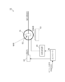
- FIG. 10 is a block diagram showing an example of a measuring device using nuclear magnetic resonance.
- a measurement apparatus using nuclear magnetic resonance (a) applies an RF (Radio Frequency) having a frequency close to the precession frequency to a measurement object 301 with a high-frequency coil 311; (b) detecting the resonating nuclear magnetization with a receiving coil 312 to generate an observation signal including a nuclear magnetic resonance (NMR) signal; (c ) The observed signal is amplified by preamplifiers 313 and 314 such as a low noise amplifier (LNA), and (d) the amplified observed signal is detected by a detector to extract an NMR signal.
- preamplifiers 313 and 314 such as a low noise amplifier (LNA)
- LNA low noise amplifier
- observation signals and NMR signals are converted from analog signals to digital signals by an analog/digital conversion circuit 315, and supplied as digital signals to a post-stage arithmetic processing device (for example, Patent Document 1, 2).
- the present invention has been made in view of the above problems, and an object of the present invention is to obtain a nuclear magnetic resonance sensing device and a nuclear magnetic resonance sensing method that accurately detect low-level NMR signals and have high resolution.
- a nuclear magnetic resonance sensing apparatus includes a nuclear magnetic resonance sensing unit that applies an RF signal to a target object and generates an observation signal having a frequency shifted from the frequency of the RF signal by the frequency of the nuclear magnetic resonance signal; A mixer unit that performs intermediate frequency demodulation of a signal to generate an intermediate frequency demodulated signal containing a nuclear magnetic resonance signal, and a high frequency band component of two band components obtained by the intermediate frequency demodulation of the intermediate frequency demodulated signal. and a low-pass filter for transmitting a low-frequency band component out of the two band components, and a digitizing device for digitizing the intermediate-frequency demodulated signal that has passed through the low-pass filter.
- the digitizing device includes a physical field generator that generates a magnetic field or an electric field corresponding to an intermediate frequency demodulated signal that has passed through a low-pass filter, a sensing member that generates light corresponding to the magnetic field or electric field, and a photoelectric element that emits the light.
- An optical quantum sensor unit for converting into an electrical signal as a sensor signal, and an analog-to-digital converter for digitizing the sensor signal, wherein the optical quantum sensor unit performs quantum operations on the sensing member to Light corresponding to the magnetic or electric field described above is generated in the sensing member.
- a nuclear magnetic resonance sensing apparatus applies a high-frequency magnetic field based on an RF signal to a target object, and generates an observation signal having a frequency shifted from the frequency of the RF signal by the frequency of the nuclear magnetic resonance signal.
- a mixer section for performing intermediate frequency demodulation of the observed signal to generate an intermediate frequency demodulated signal containing nuclear magnetic resonance signals; and a frequency of the intermediate frequency demodulated signal higher than the intermediate frequency of the intermediate frequency demodulated
- a low-pass filter that attenuates the nuclear magnetic resonance signal and transmits the frequency component of the nuclear magnetic resonance signal, and quadrature phase detection is performed on the intermediate frequency demodulated signal that has passed through the low-pass filter to generate the demodulated signal of the nuclear magnetic resonance signal and the demodulated signal.
- the digitizing device includes a first physical field generator that generates a magnetic field or an electric field corresponding to the demodulated signal, a second physical field generator that generates a magnetic field or an electric field that corresponds to the demodulated signal, and a second 1.
- Light corresponding to the magnetic field or electric field generated by the physical field generator is generated by the first sensing member, and the light generated by the first sensing member is converted into an electric signal as the first sensor signal by the first photoelectric element.
- a second sensing member generates light corresponding to a magnetic field or an electric field generated by a first optical quantum sensor unit for conversion and a second physical field generator, and the light generated by the second sensing member is transmitted to a second photoelectric conversion device.
- a second optical quantum sensor portion for converting into an electrical signal as a second sensor signal; a first analog/digital converter for digitizing the first sensor signal; and a second analog/digital converter for digitizing the second sensor signal. and a digital converter.
- the first optical quantum sensor section and the second optical quantum sensor section perform quantum operations on the first and second sensing members, respectively, to generate light corresponding to the magnetic or electric fields described above into the first and second optical quantum sensor sections. 2 generated in the sensing member.
- a nuclear magnetic resonance sensing method includes the steps of applying an RF signal to a target object, generating an observation signal having a frequency shifted from the frequency of the RF signal by the frequency of the nuclear magnetic resonance signal; a step of performing demodulation to generate an intermediate frequency demodulated signal containing a nuclear magnetic resonance signal; a step of attenuating and transmitting a low-frequency band component of the two band components; and a digitizing step of digitizing the intermediate-frequency demodulated signal that has passed through the low-pass filter with a digitizing device.
- the digitizing step (a) a magnetic or electric field corresponding to the intermediate frequency demodulated signal passed through the low-pass filter is generated, (b) light corresponding to the magnetic or electric field is generated by the sensing member, and (c) the light is The photoelectric element converts the sensor signal into an electrical signal, and (d) the analog/digital converter digitizes the sensor signal.
- quantum operations are performed on the sensing member to generate light in the sensing member that corresponds to the magnetic or electric field.
- a nuclear magnetic resonance sensing method includes the steps of applying a high-frequency magnetic field based on an RF signal to a target object and generating an observation signal having a frequency shifted from the frequency of the RF signal by the frequency of the nuclear magnetic resonance signal; performing intermediate frequency demodulation of the observed signal to produce an intermediate frequency demodulated signal containing the nuclear magnetic resonance signal; and transmitting the frequency component of the nuclear magnetic resonance signal; and performing quadrature phase detection on the intermediate frequency demodulated signal that has passed through the low-pass filter in an analog circuit to generate the demodulated signal of the nuclear magnetic resonance signal and the demodulated signal. and a digitizing step of digitizing the demodulated signal and the demodulated signal.
- a nuclear magnetic resonance sensing device and a nuclear magnetic resonance sensing method that accurately detect low-level NMR signals and have high resolution are obtained.
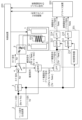
- FIG. 1 is a block diagram showing the configuration of a nuclear magnetic resonance sensing device according to Embodiment 1 of the present invention.
- FIG. 2 is a block diagram showing the configuration of the digitizing device 21 in FIG.
- FIG. 3 is a diagram showing the configuration of the sensor main body 51 in the digitizing device according to the first embodiment.
- FIG. 4 is a diagram explaining an example of a sensor signal in the digitizing device according to the first embodiment.
- FIG. 5 is a diagram showing the configuration of the sensor main body 51 in the digitizing device according to the second embodiment.
- FIG. 6 is a block diagram showing the configuration of a nuclear magnetic resonance sensing device according to Embodiment 4 of the present invention.
- FIG. 1 is a block diagram showing the configuration of a nuclear magnetic resonance sensing device according to Embodiment 1 of the present invention.
- FIG. 2 is a block diagram showing the configuration of the digitizing device 21 in FIG.
- FIG. 3 is a diagram showing the configuration of the sensor main body 51 in the digitizing device according
- FIG. 7 is a block diagram showing the configuration of the digitizing device 221 in the nuclear magnetic resonance sensing device according to the fourth embodiment.
- FIG. 8 is a block diagram showing the configuration of the digitizing device 221 in the nuclear magnetic resonance sensing device according to the fifth embodiment.
- FIG. 9 is a diagram showing the configuration of the sensor main bodies 251 and 271 of the digitizing device 202 according to the fifth embodiment.
- FIG. 10 is a block diagram showing an example of a measuring device using nuclear magnetic resonance.
- FIG. 1 is a block diagram showing the configuration of a nuclear magnetic resonance sensing device according to Embodiment 1 of the present invention.
- This nuclear magnetic resonance sensing device is used for molecular structural analysis of a target object, imaging, and the like.
- the nuclear magnetic resonance sensing device shown in FIG. 1 The nuclear magnetic resonance sensing device shown in FIG.
- the nuclear magnetic resonance sensing unit 1 applies an RF signal, which will be described later, to a target object, and observes a frequency (f RF +f NMR ) shifted from the frequency f RF of the RF signal by the frequency f NMR of a nuclear magnetic resonance (NMR) signal. Generates a signal (analog electrical signal).
- the nuclear magnetic resonance sensing section 1 includes a coil 11 and a magnet section 12 .
- the coil 11 applies a high-frequency magnetic field based on an RF signal to the target object 101, senses a magnetic field change based on the movement of nuclear magnetization in the target object 101, and outputs an observation signal.
- the magnet part 12 is a permanent magnet or an electromagnet, and applies a static magnetic field or a gradient magnetic field to the target object 101 .
- This observation signal contains the NMR signal and has a frequency that is the sum of the frequency f NMR and the RF signal frequency f RF (f RF +f NMR ).
- the base signal generator 2 generates an intermediate frequency (IF) base signal having a single intermediate frequency f IF and an RF base signal having a single frequency that is the sum of the RF band frequency f RF and the intermediate frequency f IF . is generated and output.
- IF intermediate frequency
- Mixer section 3 mixes the RF base signal and the IF base signal to generate an RF signal having frequency fRF .
- the mixer unit 3 performs SSB (Single Side Band) modulation, and outputs the frequency (f RF +2f IF ) component of the two frequency components (f RF +2f IF ) and f RF obtained by mixing. output only the RF signal of frequency fRF .
- SSB Single Side Band
- the mixer section 3 is a DBM (Double Balanced Mixer) consisting of a diode and a phase divider.
- DBM Double Balanced Mixer
- the switching unit 4 connects the nuclear magnetic resonance sensing unit 1 side (the nuclear magnetic resonance sensing unit via the matching/tuning circuit 5) to the RF signal transmission system (the base signal generation device 2 and the mixer unit 3) and the observation unit.
- the RF signal transmission system the base signal generation device 2 and the mixer unit 3
- One of the signal receiving systems (the base signal generator 2, the mixer section 6, and the low-pass filter 7) is switched to the other.
- the switching unit 4 electrically connects the transmission system to the nuclear magnetic resonance sensing unit 1 side when transmitting the RF signal, and connects the receiving system to the nuclear magnetic resonance sensing unit 1 side when receiving the observation signal. electrically connected to the side.
- the matching/tuning circuit 5 is a circuit that performs impedance matching so as to suppress the reflection of the RF signal in the nuclear magnetic resonance sensing section 1, and frequency tuning so that the level of the NMR signal becomes favorable.
- a mixer unit 6 mixes the observed signal and the RF base signal, performs intermediate frequency (IF) demodulation, and performs intermediate frequency (IF) demodulation with two frequency components (2f RF +f IF +f NMR ) and (f IF ⁇ f NMR ). ) generates and outputs a demodulated signal.
- IF intermediate frequency
- IF intermediate frequency
- the mixer section 6 is a DBM consisting of a diode and a phase divider, and does not include active elements such as transistors.
- the low - pass filter 7 selects the high-frequency band component ( 2f RF +f IF +f NMR ) and transmits the low frequency band component (f IF ⁇ f NMR ) out of the two band components.
- the low-pass filter 7 is an analog filter composed only of passive elements such as capacitors, inductors, and resistors.
- the nuclear magnetic resonance sensing device shown in FIG. 1 includes a digitizing device 21 and a control device 22.
- Digitizer 21 converts the IF demodulated signal (frequency component (f IF ⁇ f NMR )) output from low-pass filter 7 from an analog signal to a digital signal.
- the control device 22 includes a computer that operates according to a control program.
- the computer includes a CPU (Central Processing Unit), ROM (Read Only Memory), RAM (Random Access Memory), etc., and loads the control program into the RAM.
- the operations described below are executed by the CPU.
- the controller 22 controls the nuclear magnetic resonance sensing unit 1 and the switching unit 4 to apply the above-described high-frequency magnetic field to the nuclear magnetic resonance sensing unit 1 and output the above-described observation signal.
- control device 22 receives the IF demodulated signal (frequency component (f IF ⁇ f NMR )) as a digital signal from the digitizing device 21, performs predetermined signal processing (extraction of the frequency component f NMR , etc.), A frequency f NMR component (that is, an NMR signal) is extracted from the IF demodulated signal (frequency component (f IF ⁇ f NMR )).
- f IF is at least 1000 times the frequency of f NMR
- f RF is at least 10 times the frequency of f IF .
- f NMR 1 kHz
- f RF 43 MHz
- f IF 1 MHz.
- FIG. 2 is a block diagram showing the configuration of the digitizing device 21 in FIG.
- the digitizing device shown in FIG. 1 includes a physical field generator 41 , an optical quantum sensor section 42 and an analog/digital converter (A/D converter, ADC) 43 .
- A/D converter ADC
- the physical field generator 41 generates a magnetic field corresponding to an input signal (that is, analog IF demodulated signal) input via the input terminal 41a of the physical field generator 41 .
- the physical field generator 41 generates the magnetic field with a conductive coil or wiring.
- the optical quantum sensor unit 42 includes a sensor main body 51 and a photoelectric element 52.
- the sensing member generates light (observation light) corresponding to the magnetic field generated by the physical field generator 41, and the photoelectric element 52 converts the light into electrical signals as sensor signals.
- the photoelectric element 52 such as a photodiode or a phototransistor, generates a sensor signal corresponding to the intensity of incident observation light.
- the optical quantum sensor unit 42 (specifically, the sensor main body 51) performs quantum manipulation (here, quantum manipulation by microwave and laser light) on the sensing member to generate a physical field generator. Light corresponding to the magnetic field generated at 41 is generated in the sensing member.
- the optical quantum sensor unit 42 (specifically, the sensor main body 51) performs quantum manipulation on the sensing member according to the optical detection magnetic resonance measurement (ODMR) method to emit the above observation light. Generated in the sensing member.
- ODMR optical detection magnetic resonance measurement
- FIG. 3 is a diagram showing the structure of the sensor main body 51 in the digitizing device according to Embodiment 1.
- the sensor main body 51 includes a magnetic resonance member 61 as a sensing member, a high frequency magnetic field generator 62, a magnet 63, a high frequency power supply 64, a light emitting device 65 , and a controller 66 .
- the magnetic resonance member 61 has a crystalline structure, the electron spin quantum state changes in response to the magnetic field generated by the physical field generator 41, and microwaves with a frequency corresponding to the arrangement direction of defects and impurities in the crystal lattice are generated. is a possible member of electron spin quantum manipulation (based on Rabi oscillations). That is, the magnetic resonance member 61 is arranged within the magnetic field described above.
- the magnetic resonance member 61 is a light-detecting magnetic resonance member having a plurality (that is, ensemble) of specific color centers.
- the specific color center has an energy level capable of Zeeman splitting, and can take a plurality of directions with mutually different shift widths of the energy level upon Zeeman splitting.
- the magnetic resonance member 61 is a member such as a diamond including a plurality of NV (Nitrogen Vacancy) centers as single type specific color centers.
- the color center included in the magnetic resonance member 61 may be a color center other than the NV center.
- the high-frequency magnetic field generator 62 applies microwaves to the magnetic resonance member 61 to perform electron spin quantum manipulation of the magnetic resonance member 61 .
- the high-frequency magnetic field generator 62 is a plate-like coil, and includes a substantially circular coil portion that emits microwaves, and terminal portions that extend from both ends of the coil portion and are fixed to the substrate.
- the high frequency power supply 64 generates the microwave current and conducts it to the high frequency magnetic field generator 62 .
- the coil section conducts two currents parallel to each other at a predetermined interval so as to sandwich the magnetic resonance member 61 at both end surfaces of the coil section, and emits the microwaves described above.
- the coil portion is a plate-like coil, and due to the skin effect, the microwave current flows through the end face portion of the coil portion, so that two currents are formed. As a result, microwaves of substantially uniform intensity are applied to the magnetic resonance member 61 .
- NV centers color centers are formed by defects (vacancies) (V) and nitrogen (N) as impurities in the diamond crystal.
- N defects
- N nitrogen
- energy levels are different from each other. Therefore, in the characteristics of the fluorescence intensity after Zeeman splitting due to the static magnetic field with respect to the microwave frequency, four different dip frequency pairs (fi+, fi-) appears.
- the above-described microwave frequency (wavelength) is set corresponding to one of the dip frequencies of the four dip frequency pairs.
- the magnet 63 applies a static magnetic field (direct current magnetic field) to the magnetic resonance member 61 to Zeeman split the energy levels of a plurality of specific color centers (here, a plurality of NV centers) within the magnetic resonance member 61 .
- the magnet 63 is a ring-shaped permanent magnet such as a ferrite magnet, an alnico magnet, or a samarium-cobalt magnet. Note that the magnet 63 may be an electromagnet.
- the crystals of the magnetic resonance member 61 are formed such that the alignment direction of the above-described defects and impurities substantially coincides with the above-described direction of the static magnetic field (and the direction of the applied magnetic field).
- the orientation of member 61 is set.
- an optical system (not shown) is provided from the light emitting device 65 to the magnetic resonance member 61 in order to irradiate the magnetic resonance member 41 with excitation light.
- An optical system (not shown) is provided from the magnetic resonance member 61 to the photoelectric element 52 in order to detect fluorescence (observation light) from the magnetic resonance member 61 .
- the observation light is condensed toward the photoelectric element 52 by an optical system such as a compound parabolic concentrator (CPC).
- CPC compound parabolic concentrator
- the magnetic resonance member 61 is arranged on the CPC, and the fluorescence emitted in all directions from the color center in the magnetic resonance member 61 is emitted in a wide solid angle (for example, a predetermined ratio or more in all directions) by this optical system.
- the emitted fluorescence is collected.
- the light emitting device 65 includes a laser diode or the like as a light source, and emits laser light of a predetermined wavelength as excitation light to be irradiated to the magnetic resonance member 61 from the light source.
- the controller 66 controls (a) the high-frequency power supply 64 and the light-emitting device 65 according to a predetermined measurement sequence to perform quantum manipulation with the above-described microwaves and laser beams to generate observation light in the sensor body 51, thereby generating photoelectric A sensor signal is generated at the element 52 .
- the controller 66 includes a computer that operates according to the control program, and the computer includes a CPU, ROM, RAM (Random Access Memory), etc. By loading the control program into the RAM and executing it on the CPU, the above-mentioned perform an action.
- the controller 66 may be built in the control device 22 , or the control device 22 may operate as the controller 66 .
- FIG. 4 is a diagram explaining an example of a sensor signal in the digitizing device according to Embodiment 1.
- FIG. This measurement sequence is set according to the above frequency of the magnetic field and the like.
- the input signal IF demodulated signal
- the input signal is an AC signal with a relatively low frequency (for example, several tens of Hz)
- the DC magnetic field measurement sequence SQ1 to SQn the above-described magnetic field measurements corresponding to the input signals are performed, and the measured values BM1 to BMn are obtained as sensor signals.
- a spin echo pulse sequence (such as a Hahn echo sequence) is applied to this measurement sequence.
- the measurement sequence is not limited to these, and may be selected according to the frequency of the magnetic field to be measured.
- the measurement sequence is not limited to these, and may be selected according to the frequency of the magnetic field to be measured.
- the magnetic field measurement is performed with a plurality of Ramsay pulse sequences as described above, and when the period of the magnetic field described above is shorter than the T2 relaxation time, A spin echo pulse sequence (such as a Hahn echo sequence) may be applied.
- the magnetic field may be measured according to the Qdyne method.
- the A/D converter 43 digitizes the above sensor signal (without digitizing the input signal), thereby producing a digital signal as an output signal corresponding to the input signal (IF demodulated signal). It is generated and output via the output terminal 43a of the A/D converter 43.
- the optical quantum sensor section 42 (specifically, the sensor main body 51) senses the observation light described above so that the level of the sensor signal exceeds the noise floor of the A/D converter 43. generated in the member.
- the efficiency of the sensing member in the first embodiment, the type and number of color centers in the magnetic resonance member 61
- the observation light collection efficiency in the first embodiment, the photoelectric element 52 with respect to the amount of light emitted by the color center
- the level (amplitude) of the sensor signal changes depending on factors such as the amount of incident light to the sensor), the conversion efficiency of the photoelectric element 52 (the level of the sensor signal with respect to the amount of incident light), and so on. ), the values of these factors are determined such that the level of the sensor signal exceeds the noise floor of the A/D converter 43 .
- the sensitivity of the optical quantum sensor section 42 is set to 1.5 pT/Hz 1/2 or more.
- A/D converter noise includes quantization noise and thermal noise, and in high-resolution A/D converters, thermal noise is dominant over quantization noise.
- the A/D converter 43 in this embodiment is a high-resolution A/D converter, and the values of the above factors are determined so that the level of the sensor signal exceeds the noise level of thermal noise.
- the reference voltage of the A/D converter 43 is set according to the range of the sensor signal (minimum level value and maximum level value). By lowering the reference voltage of the A/D converter, quantization noise is reduced, but thermal noise is not reduced.
- the level (or range) of the input demodulated IF signal and the electromagnetic conversion efficiency of the physical field generator 41 are known.
- the digitizing device 21 does not particularly include an amplifier circuit between the photoelectric element 52 and the A/D converter 43 for electrically increasing the sensor signal. Furthermore, in this embodiment, an amplifier circuit for electrically increasing the input signal is not provided between the signal source of the input signal and the physical field generator 41 . In other words, in this embodiment, an electrical amplifier circuit that becomes a noise source is not provided on the upstream side of the A/D converter 43 . In such an amplifier circuit, thermal noise is generated and amplified in the same manner as in the A/D converter 43, so noise is superimposed on the signal input to the A/D converter 43. Preferably not provided.
- the high-frequency power supply 64 and the controller 66 are electrically separated from the A/D converter 43 so that electrical noise generated by the high-frequency power supply 64 and the controller 66 does not enter the A/D converter 43. It's becoming
- the mixer unit 6 performs intermediate frequency demodulation of the observation signal with the RF base signal to generate an IF demodulated signal containing the NMR signal
- the optical quantum sensor unit 42 uses the IF base signal as a synchronizing signal and periodically repeats according to the synchronizing signal to perform quantum operations on the sensing member to cause the sensing member to generate light corresponding to the magnetic field, thereby causing the digitizing device 21 to , to output a digital IF demodulated signal in synchronization with the IF base signal.
- the controller 22 Based on this digital IF demodulated signal, the controller 22 accurately identifies the frequency fNMR of the NMR signal according to the Qdyne method.
- the control device 22 controls the nuclear magnetic resonance sensing unit 1 and controls the switching unit 4 so that the nuclear magnetic resonance sensing unit 1 applies a high-frequency magnetic field based on the RF signal from the transmission system to the target object 101,
- the switching unit 4 is controlled to conduct the observation signal from the nuclear magnetic resonance sensing unit 1 to the receiving system.
- the observed signal is converted into an IF demodulated signal by the mixer section 6, and the IF demodulated signal from which the components on the high frequency side are removed by the low-pass filter 7 is input to the digitizing device 21. .
- the physical field generator 41 when the IF demodulated signal is applied to the physical field generator 41 , the physical field generator 41 generates a magnetic field with a strength corresponding to the level of the input signal, and the sensor body of the optical quantum sensor section 42 . 51.
- the measurement sequence is executed as described above, and the amount of light corresponding to the strength of the magnetic field is generated.
- the magnetic resonance member 61 is caused to generate light in an amount corresponding to the strength of the magnetic field.
- the photoelectric element 52 receives the light, generates a sensor signal having a level corresponding to the amount of received light, and outputs it to the A/D converter 43 .
- the A/D converter 43 digitizes the sensor signal, generates a digital IF demodulated signal corresponding to the analog IF demodulated signal, and outputs it to the control device 22 .
- the controller 22 continuously and repeatedly obtains the value of the digital IF demodulated signal, derives the NMR signal (specifically, f NMR , etc.) by signal processing as described above, and based on the NMR signal Then, molecular structure analysis, imaging, and the like of the target object 101 are performed.
- the NMR signal specifically, f NMR , etc.
- the nuclear magnetic resonance sensing unit 1 applies an RF signal to the target object 101, and detects the sum of the frequency of the RF signal and the frequency of the nuclear magnetic resonance signal. generate an observed signal with
- the mixer unit 6 performs IF demodulation of the observed signal to generate an IF demodulated signal containing nuclear magnetic resonance signals.
- the low-pass filter 7 attenuates the high frequency band component of the two band components obtained by IF demodulation in the IF demodulated signal, and transmits the low frequency band component of the two band components.
- a digitizing device 21 digitizes the IF demodulated signal that has passed through the low-pass filter 7 .
- the physical field generator 41 generates a magnetic field or electric field corresponding to the intermediate frequency demodulated signal passed through the low-pass filter 7, and the optical quantum sensor unit 42 senses light corresponding to the magnetic field or electric field.
- the light generated by the member is converted into an electric signal as a sensor signal by a photoelectric element, and the analog/digital converter 43 digitizes the sensor signal.
- the optical quantum sensor unit 42 performs quantum operations on the sensing member described above to cause the sensing member to generate light corresponding to the magnetic or electric field described above.
- a sensor signal with a relatively large level corresponding to a weak IF demodulated signal is obtained and digitized.
- a signal (digital signal) can be obtained with high accuracy. Therefore, a minute IF demodulated signal whose level is equal to or lower than the noise level of the A/D converter 43 is accurately digitized. As a result, it is possible to accurately detect low-level NMR signals and perform high-resolution nuclear magnetic resonance sensing.
- the optical quantum sensor unit 42 performs quantum manipulation on the sensing member according to optically pumped atomic magnetometry (OPAM) instead of ODMR to emit light corresponding to the magnetic field to the sensing member. generate.
- OPAM optically pumped atomic magnetometry
- FIG. 5 is a diagram showing the configuration of the sensor main body 51 in the digitizing device according to Embodiment 2. As shown in FIG. In Embodiment 2, the sensor main body 51 includes a cell 71, a magnet 72, and light emitting devices 73 and 74 for OPAM.
- the cell 71 is a transparent glass cell or the like, and alkali metal atoms (K, Rb, Cs, etc.) as the sensing member 71a are enclosed in the cell 71 together with a buffer gas.
- the magnet 72 is a magnet that applies static magnetism to the sensing member, and may be a permanent magnet as described above or an electromagnet.
- the light emitting device 73 generates pump light and irradiates the sensing member 71a with it.
- the light emitting device 74 generates probe light and irradiates the sensing member 71a with the probe light.
- spin polarization is induced in the sensing member by optical pumping with the pump light, and the rotation of the spin polarization in response to the magnetic field is measured by the magneto-optical rotation of the probe light.
- the deflection rotation angle of observation light that is, probe light after magneto-optical rotation
- the deflection rotation angle of the observation light is detected by a plurality of photoelectric elements 52 by the 4-detector method or the like.
- the sensor signals are digitized by a plurality of A/D converters 43, converted into a plurality of digital signals, and then arithmetically processed (difference calculation, etc.).
- Embodiment 2 The rest of the configuration and operation of the nuclear magnetic resonance sensing apparatus according to Embodiment 2 are the same as those in Embodiment 1, so description thereof will be omitted.
- the physical field generator 41 generates an electric field corresponding to an input signal (that is, an analog IF demodulated signal) input via the input terminal 41a of the physical field generator 41, and optical quantum
- the sensor unit 42 generates light (observation light) corresponding to the electric field generated by the physical field generator 41 using the sensing member, and the photoelectric element 52 converts the light into an electric signal as a sensor signal. do.
- the physical field generator 41 generates the electric field with a pair of electrode plates.
- the input signal may be an AC signal with a single frequency, an AC signal having a plurality of frequency components and a predetermined cycle, or a DC signal. That is, the electric field described above can be a single-frequency AC electric field, a predetermined period AC electric field having a plurality of frequency components, a DC electric field, or the like, depending on the input signal.
- the sensing member used in ODMR and OPAM is one whose quantum state is changed by an electric field and whose electric field can be measured by a similar measurement sequence.
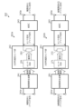
- FIG. 6 is a block diagram showing the configuration of a nuclear magnetic resonance sensing device according to Embodiment 4 of the present invention.
- the nuclear magnetic resonance sensing apparatus includes a nuclear magnetic resonance sensing section 1, a base signal generation device 2, a mixer section 3, a switching section 4, a matching ⁇ In addition to the tuning circuit 5, the mixer section 6, and the low-pass filter 7, the analog quadrature detection circuit 201, the digitizing device 202, and the control device 203 are provided.
- the analog quadrature detection circuit 201 performs quadrature detection on the intermediate frequency demodulated signal that has passed through the low-pass filter 7 to generate a demodulated signal I of the nuclear magnetic resonance signal and a demodulated signal Q.
- analog quadrature detection circuit 201 includes 90-degree phase shifter 211 , mixer sections 212 and 213 , and low-pass filters 214 and 215 .
- a 90-degree phase shifter 211 shifts the phase of the IF base signal by 90 degrees. Note that the 90-degree phase shifter 211 may be an analog circuit and may not include active elements.
- Mixer section 212 mixes and demodulates the IF demodulated signal and the IF base signal to generate and output a demodulated signal having two frequency components (2f IF ⁇ f NMR ) and f NMR .
- the low-pass filter 214 attenuates the two band components (2f IF ⁇ f NMR ) obtained by the demodulation of the mixer section 212 and the high frequency band component (2f IF ⁇ f NMR ) of the f NMR in the demodulated signal. , and a filter that transmits a low-frequency band component (f NMR ) out of the two band components.
- Mixer section 213 mixes and demodulates the IF demodulated signal and the 90-degree phase-shifted IF base signal to generate and output a demodulated signal having two frequency components (2f IF ⁇ f NMR ) and f NMR .
- the low-pass filter 215 attenuates the two band components (2f IF ⁇ f NMR ) obtained by demodulation of the mixer section 213 and the high frequency band component (2f IF ⁇ f NMR ) of the f NMR in the demodulated signal. , and a filter that transmits a low-frequency band component (f NMR ) out of the two band components.
- the low-pass filters 214 and 215 are analog filters composed only of passive elements such as capacitors, inductors, and resistors.
- the mixer units 212 and 213 are DBMs composed of diodes and phase dividers.
- the digitizing device 202 digitizes the demodulated signal I and the demodulated signal Q (frequency component f NMR ), and converts them from analog signals to digital signals.
- the control device 203 includes a computer that operates according to a control program, and the computer includes a CPU, ROM, RAM, etc.
- the control program is loaded into the RAM and executed by the CPU, thereby executing operations described later.
- the control device 203 controls the nuclear magnetic resonance sensing section 1 and the switching section 4 to cause the nuclear magnetic resonance sensing section 1 to apply the high-frequency magnetic field described above. Output the observation signal.
- the control device 203 receives the demodulated signal I and the demodulated signal Q (frequency component f NMR ) as digital signals from the digitizing device 202 and performs predetermined signal processing to generate an NMR signal (frequency component f NMR ). Extract.
- FIG. 7 is a block diagram showing the configuration of the digitizing device 221 in the nuclear magnetic resonance sensing device according to the fourth embodiment.
- the digitizing device 202 shown in FIG. 7 includes a digitizing section 202a that digitizes the demodulated signal I and a digitizing section 202b that digitizes the demodulated signal Q.
- the digitizing section 202a performs digitizing.
- the digitizing unit 202a includes a physical field generator 241 similar to the physical field generator 41, an optical quantum sensor unit 242 similar to the optical quantum sensor unit 42, and an A/D converter similar to the A/D converter 43. and a vessel 243 .
- the digitizing unit 202b includes a physical field generator 261 similar to the physical field generator 41, an optical quantum sensor unit 262 similar to the optical quantum sensor unit 42, and an A/D converter 43 similar to the A/D converter 43. and a D converter 263 .
- the physical field generators 241 and 261 respectively generate magnetic fields corresponding to the input signals (that is, analog IF demodulated signals) input via the input terminals 241a and 261a of the physical field generators 241 and 261.
- the physical field generators 241 and 261 generate the magnetic fields with conductive coils and wires.
- the optical quantum sensor units 242 and 262 include sensor bodies 251 and 271 similar to the sensor body 51 and photoelectric elements 252 and 272 similar to the photoelectric element 52, respectively.
- the sensing member generates light (observation light) corresponding to the magnetic field generated by 241 and 261, and photoelectric elements 252 and 272 convert the light into electrical signals as sensor signals.
- the photoelectric elements 252, 272, such as photodiodes or phototransistors, generate sensor signals corresponding to the intensity of incident observation light.
- the optical quantum sensor units 242 and 262 (specifically, the sensor main bodies 251 and 271) perform quantum operations on the sensing members according to optical detection magnetic resonance measurement (ODMR), respectively,
- ODMR optical detection magnetic resonance measurement
- an optical system from the light emitting device to the magnetic resonance member is provided in the optical quantum sensor units 242 and 262 in order to irradiate the magnetic resonance member with excitation light.
- An optical system is provided from the magnetic resonance member to the photoelectric element in order to detect fluorescence (observation light) from the magnetic resonance member.
- optical quantum sensor units 242 and 26 each follow a predetermined measurement sequence to (a) control the high-frequency power source and the light emitting device to generate quantum light with microwaves and laser light.
- An operation is performed to cause the sensor bodies 251 and 271 to generate observation light and the photoelectric elements 252 and 272 to generate sensor signals.
- This measurement sequence is set according to the frequency of the magnetic field, etc., as in the first embodiment.
- A/D converters 243 and 263 digitize the sensor signal output from optical magnetic sensor section 242 (without directly digitizing analog demodulated signal I and demodulated signal Q), thereby demodulating A digital signal is generated as an output signal corresponding to the signal I and the demodulated signal Q, and is output via output terminals 243a and 263a of the A/D converters 243 and 263, respectively.
- the optical quantum sensor units 242, 262 are configured such that the level of the sensor signal exceeds the noise floor of the A/D converters 243, 263.
- the sensing member is caused to generate the observation light described above.
- factors such as the efficiency of the sensing member, the efficiency of collecting the observation light, and the conversion efficiency of the photoelectric elements 252 and 272 affect the level of the sensor signal to the noise floor of the A/D converter 43. (known), it is determined to exceed the noise floor of the A/D converter 43 .
- the sensitivity of the optical quantum sensor units 242 and 262 is set to 1.5 pT/Hz 1/2 or more.
- the A/D converters 243 and 263 in this embodiment are high-resolution A/D converters, and the values of the above factors are determined so that the level of the sensor signal exceeds the noise level of thermal noise. be done.
- the reference voltages of the A/D converters 243 and 263 are set according to the range (minimum level and maximum level) of the sensor signal.
- the levels (or ranges) of the input demodulated signal and demodulated signal and the electromagnetic conversion efficiency of the physical field generators 241 and 261 are known.
- the digitizing device 202 does not include an amplifier circuit between the photoelectric elements 252 and 272 and the A/D converters 243 and 263 to electrically increase the sensor signal. Furthermore, in this embodiment, an amplifier circuit for electrically increasing the input signal is not provided between the signal source of the input signal and the physical field generators 241 and 261 . In other words, in this embodiment, no electrical amplifier circuit that becomes a noise source is provided upstream of the A/D converters 243 and 263 .
- optical quantum sensor units 242, 262 and the A/D converters 243, 263 are electrically separated, and the electrical noise generated in the optical quantum sensor units 242, 262 is generated by the A/D converter. 243 and 263.
- the control device 203 controls the nuclear magnetic resonance sensing unit 1 and controls the switching unit 4 so that the nuclear magnetic resonance sensing unit 1 applies a high-frequency magnetic field based on the RF signal from the transmission system to the target object 101,
- the switching unit 4 is controlled to conduct the observation signal from the nuclear magnetic resonance sensing unit 1 to the receiving system.
- the observed signal is converted into an IF demodulated signal by the mixer section 6, and the IF demodulated signal from which the high-frequency band side components are removed by the low-pass filter 7 is sent to the analog quadrature detection circuit 201. is entered.
- Quadrature detection circuit 201 performs quadrature detection on the IF demodulated signal using the IF base signal to generate demodulated signal I and demodulated signal Q of frequency component f NMR , and inputs them to digitizer 202 .
- the physical field generator 241 when the demodulated signal I is applied to the physical field generator 241, the physical field generator 241 generates a magnetic field with a strength corresponding to the level of the input signal, and the sensor main body of the optical quantum sensor section 242 251.
- the measurement sequence is executed as described above, and the amount of light corresponding to the strength of the magnetic field is generated.
- the magnetic resonance member is caused to generate light in an amount corresponding to the strength of the magnetic field.
- the photoelectric element 252 receives the light, generates a sensor signal having a level corresponding to the amount of received light, and outputs it to the A/D converter 243 .
- the A/D converter 243 digitizes the sensor signal to generate a digital demodulated signal I corresponding to the analog demodulated signal I and outputs it to the control device 203 .
- the physical field generator 261 when the demodulated signal Q is applied to the physical field generator 261, the physical field generator 261 generates a magnetic field with a strength corresponding to the level of the input signal, It is applied to the sensor main body 271 of the target quantum sensor section 262 .
- the measurement sequence is executed as described above, and the amount of light corresponding to the strength of the magnetic field is generated.
- the magnetic resonance member is caused to generate light in an amount corresponding to the strength of the magnetic field.
- the photoelectric element 272 receives the light, generates a sensor signal having a level corresponding to the amount of received light, and outputs it to the A/D converter 263 .
- the A/D converter 263 digitizes the sensor signal to generate a digital demodulated signal Q corresponding to the analog demodulated signal Q and outputs it to the control device 203 .
- the control device 203 continuously and repeatedly obtains the values of the digital demodulated signal I and the demodulated signal Q at each point in time, and performs signal processing as described above to obtain an NMR signal (specifically, f NMR or the like) or A chemical shift is derived, and based on the NMR signal and chemical shift, the molecular structure analysis, imaging, etc. of the target object 101 are performed.
- NMR signal specifically, f NMR or the like
- a chemical shift is derived, and based on the NMR signal and chemical shift, the molecular structure analysis, imaging, etc. of the target object 101 are performed.
- Embodiment 4 The rest of the configuration and operation of the nuclear magnetic resonance sensing apparatus according to Embodiment 4 are the same as those of Embodiments 1 to 3, so description thereof will be omitted.
- the analog quadrature detection circuit 201 performs quadrature detection on the intermediate frequency demodulated signal that has passed through the low-pass filter 7, and performs the demodulated signal I of the nuclear magnetic resonance signal and the subject signal.
- a demodulated signal Q is generated.
- a digitizing device 202 digitizes the demodulated signal I and the demodulated signal Q.
- FIG. In the digitizing device 202 physical field generators 241 and 261 generate magnetic or electric fields corresponding to the demodulated signal and the demodulated signal, respectively. , 261 generate light corresponding to the magnetic field or electric field generated by the sensing members, respectively, and the light generated by the sensing members is converted into electrical signals as first and second sensor signals by photoelectric elements 252 and 272.
- A/D converters 243 and 263 digitize the first and second sensor signals, respectively.
- the optical quantum sensor units 242 and 262 respectively perform quantum operations on the sensing member to cause the sensing member to generate light corresponding to the magnetic or electric field described above.
- the target nuclear magnetic resonance signal and the chemical shift are distinguished from each other and detected based on the demodulated signal I and the demodulated signal Q by analysis in the control device 203 .
- nuclear magnetic resonance sensing with high resolution can be performed by accurately detecting low-level nuclear magnetic resonance signals.
- FIG. 8 is a block diagram showing the configuration of the digitizing device 221 in the nuclear magnetic resonance sensing device according to the fifth embodiment.
- the optical quantum sensor units 242 and 262 irradiate the respective sensing members with a common laser beam (the excitation light described above) to perform the quantum operation described above.
- light corresponding to the magnetic field or electric field generated by the physical field generators 241 and 261 is generated in each sensing member.
- FIG. 9 is a diagram showing the configuration of the sensor main bodies 251 and 271 of the digitizing device 202 according to the fifth embodiment.
- high-frequency magnetic field generators 292a, 292b, and magnets 293a, 293b for example, as shown in FIG. , high-frequency magnetic field generators 292a, 292b, and magnets 293a, 293b.
- a high-frequency power source 294, a light-emitting device 295, and a controller 296 are a single high-frequency power source, light-emitting device, and controller common to the two systems of magnetic resonance members 291a and 291b and high-frequency magnetic field generators 292a and 292b.
- the laser light emitted from the light emitting device 295 is processed by an optical system (not shown) to be used as a laser light incident on the magnetic resonance member 291a, a laser light incident on the magnetic resonance member 291b, and a reference light described later. is branched to
- the magnetic resonance members 291a and 291b, the high frequency magnetic field generators 292a and 292b, the magnets 293a and 293b, the high frequency power supply 294, the light emitting device 295, and the controller 296 are connected to the magnetic resonance member 61, the high frequency magnetic field generator 62, and the magnet 63. , high frequency power supply 64 , light emitting device 65 and controller 66 .
- sensor body 251 includes high frequency power source 294, light emitting device 295, and controller 296, but instead, sensor body 271 includes high frequency power source 294, light emitting device 295, and controller 296.
- the digitizing device 202 includes a photoelectric element 281 and differential circuits 282 and 283 as analog circuits.
- the photoelectric element 281 converts the reference light branched from the common laser light into an electric signal as a third sensor signal.
- the photoelectric element 281 is a photodiode, a phototransistor, or the like.
- the difference circuit 282 performs common mode rejection on the sensor signal (first sensor signal) of the optical quantum sensor section 242 based on the third sensor signal. Specifically, the difference circuit 282 subtracts the third sensor signal from the first sensor signal and inputs the subtracted first sensor signal to the A/D converter 243 . Further, the difference circuit 283 performs common mode rejection on each sensor signal (second sensor signal) of the optical quantum sensor section 262 based on the third sensor signal. Specifically, the difference circuit 283 subtracts the third sensor signal from the second sensor signal and inputs the subtracted second sensor signal to the A/D converter 263 .
- photoelectric element 281 and the difference circuits 282 and 283 may or may not be provided as required.
- the optical quantum sensor units 242 and 262 use a single light emitting device 295 to irradiate the magnetic resonance members 291a and 291b of the sensor bodies 251 and 271 with common excitation light. Then, a first sensor signal corresponding to the demodulated signal I and a second sensor signal corresponding to the demodulated signal Q are generated and output, and a third sensor signal corresponding to the reference light is generated and output.
- Difference circuits 282 and 283 subtract the third sensor signal from the first sensor signal and the second sensor signal, respectively, and input the subtracted first sensor signal and the second sensor signal to A/D converters 243 and 263, respectively. do.
- Embodiment 5 The rest of the configuration and operation of the nuclear magnetic resonance sensing device according to Embodiment 5 are the same as those in Embodiment 4, so description thereof will be omitted.
- a single laser beam is used as excitation light common to the magnetic resonance members 291a and 291b. deviation is suppressed. Also, the noise component contained in the first sensor signal and the second sensor signal due to the noise component contained in the laser light generated by the light emitting device 295 is suppressed.
- the measurement method in the sensor main bodies 51, 251, 271 is not limited to the above-described ODMR and OPAM, and uses a sensing member according to the physical field to perform quantum manipulation on the sensing member.
- Other measurement methods may be used as long as they can detect observation light corresponding to the physical field intensity.
- control device 22 controls the output signals of the digitizing devices 21 and 202 so that the values (digital values) of the output signals match the levels of the analog IF demodulated signals. may be performed.
- the present invention is applicable, for example, to various measurements and imaging using nuclear magnetic resonance.
- nuclear magnetic resonance sensing unit 2 base signal generator 3 mixer unit (an example of a transmission system mixer unit) 6 mixer section 7 low-pass filter 21, 202 digitizing device 41 physical field generator 42 optical quantum sensor section 43 analog/digital converter 52, 252, 272 photoelectric element 101 target object 201 quadrature detection circuit 241 physical field generator (first 1 An example of a physical field generator) 242 optical quantum sensor unit (an example of the first optical quantum sensor unit) 243 analog/digital converter (an example of a first analog/digital converter) 261 physical field generator (an example of the second physical field generator) 262 optical quantum sensor unit (an example of a second optical quantum sensor unit) H.263 analog/digital converter (an example of a second analog/digital converter) 281 photoelectric element (an example of the third photoelectric element) 282 difference circuit (an example of the first difference circuit) 283 difference circuit (an example of a second difference circuit)
Abstract
[Problem] To perform nuclear magnetic resonance sensing by which a low-level NMR signal is accurately detected and which has high resolution. [Solution] A nuclear magnetic resonance sensing unit 1 applies, to a target object, a high-frequency magnetic field which is based on an RF signal, and generates an observation signal the frequency of which is shifted from the frequency of said RF signal by the frequency of an NMR signal. A mixer unit 6 generates an IF demodulated signal that includes the NMR signal. A low-pass filter 7 transmits a low-frequency band component of the IF demodulated signal. In a digitizing device 21, a physical field generation device generates a magnetic field etc. corresponding to the IF demodulated signal that has been transmitted through the low-pass filter 7, an optical quantum sensor unit uses a sensing member to generate light corresponding to said magnetic field etc. and uses a photoelectric element to convert said light to a sensor signal, and an analogue-digital converter digitizes said sensor signal. This optical quantum sensor unit subjects the above-mentioned sensing member to quantum manipulation and uses the sensing member to generate the light corresponding to the above-mentioned magnetic field etc.
Description
本発明は、核磁気共鳴センシング装置および核磁気共鳴センシング方法に関するものである。
The present invention relates to a nuclear magnetic resonance sensing device and a nuclear magnetic resonance sensing method.
図10は、核磁気共鳴を利用した測定装置の一例を示すブロック図である。例えば図10に示すように、核磁気共鳴を利用した測定装置は、一般的に、(a)測定対象301に対して、高周波コイル311で歳差運動の周波数に近い周波数を有するRF(Radio Frequency)信号に基づく高周波磁場を印加することで核磁化を共鳴させ、(b)その共鳴した核磁化を受信コイル312で検出し、核磁気共鳴(NMR)信号を含む観測信号を生成し、(c)その観測信号をローノイズアンプ(LNA)などといったプリアンプ313,314で増幅し、(d)増幅後の観測信号を検波器で検波しNMR信号を抽出している。
FIG. 10 is a block diagram showing an example of a measuring device using nuclear magnetic resonance. For example, as shown in FIG. 10, in general, a measurement apparatus using nuclear magnetic resonance (a) applies an RF (Radio Frequency) having a frequency close to the precession frequency to a measurement object 301 with a high-frequency coil 311; (b) detecting the resonating nuclear magnetization with a receiving coil 312 to generate an observation signal including a nuclear magnetic resonance (NMR) signal; (c ) The observed signal is amplified by preamplifiers 313 and 314 such as a low noise amplifier (LNA), and (d) the amplified observed signal is detected by a detector to extract an NMR signal.
また、一般的に、そのような観測信号やNMR信号は、アナログ/デジタル変換回路315で、アナログ信号からデジタル信号へ変換され、デジタル信号として、後段の演算処理装置に供給される(例えば特許文献1,2参照)。
Further, in general, such observation signals and NMR signals are converted from analog signals to digital signals by an analog/digital conversion circuit 315, and supplied as digital signals to a post-stage arithmetic processing device (for example, Patent Document 1, 2).
しかしながら、上述の装置では、観測信号を増幅するために、プリアンプなどといった増幅回路が設けられているため、増幅回路に固有なノイズが観測信号やNMR信号に重畳してしまう。このため、増幅回路のノイズフロアの同程度もしくはそれより低いレベルのNMR信号はノイズに埋もれてしまい、そのような低いレベルのNMR信号を精度良く検出することは困難である。
However, in the above-described apparatus, since an amplifier circuit such as a preamplifier is provided to amplify the observed signal, noise unique to the amplifier circuit is superimposed on the observed signal and the NMR signal. Therefore, an NMR signal with a level equal to or lower than the noise floor of the amplifier circuit is buried in noise, and it is difficult to accurately detect such a low level NMR signal.
本発明は、上記の問題に鑑みてなされたものであり、低レベルのNMR信号を精度良く検出し分解能の高い核磁気共鳴センシング装置および核磁気共鳴センシング方法を得ることを目的とする。
The present invention has been made in view of the above problems, and an object of the present invention is to obtain a nuclear magnetic resonance sensing device and a nuclear magnetic resonance sensing method that accurately detect low-level NMR signals and have high resolution.
本発明に係る核磁気共鳴センシング装置は、RF信号を対象物体に印加し、そのRF信号の周波数から核磁気共鳴信号の周波数だけシフトした周波数の観測信号を生成する核磁気共鳴センシング部と、観測信号の中間周波復調を実行して、核磁気共鳴信号を含む中間周波復調信号を生成するミキサ部と、中間周波復調信号のうち、中間周波復調で得られる2つの帯域成分のうちの高周波帯域成分を減衰させ、その2つの帯域成分のうちの低周波帯域成分を透過するローパスフィルタと、ローパスフィルタを透過した中間周波復調信号をデジタイズするデジタイズ装置とを備える。デジタイズ装置は、ローパスフィルタを透過した中間周波復調信号に対応する磁場または電場を発生する物理場発生装置と、その磁場または電場に対応する光をセンシング部材で発生し、その光を光電素子で、センサ信号としての電気信号に変換する光学的量子センサ部と、センサ信号をデジタイズするアナログ/デジタル変換器とを備え、光学的量子センサ部は、上述のセンシング部材に対して量子操作を行って、上述の磁場または電場に対応する光をセンシング部材に発生させる。
A nuclear magnetic resonance sensing apparatus according to the present invention includes a nuclear magnetic resonance sensing unit that applies an RF signal to a target object and generates an observation signal having a frequency shifted from the frequency of the RF signal by the frequency of the nuclear magnetic resonance signal; A mixer unit that performs intermediate frequency demodulation of a signal to generate an intermediate frequency demodulated signal containing a nuclear magnetic resonance signal, and a high frequency band component of two band components obtained by the intermediate frequency demodulation of the intermediate frequency demodulated signal. and a low-pass filter for transmitting a low-frequency band component out of the two band components, and a digitizing device for digitizing the intermediate-frequency demodulated signal that has passed through the low-pass filter. The digitizing device includes a physical field generator that generates a magnetic field or an electric field corresponding to an intermediate frequency demodulated signal that has passed through a low-pass filter, a sensing member that generates light corresponding to the magnetic field or electric field, and a photoelectric element that emits the light. An optical quantum sensor unit for converting into an electrical signal as a sensor signal, and an analog-to-digital converter for digitizing the sensor signal, wherein the optical quantum sensor unit performs quantum operations on the sensing member to Light corresponding to the magnetic or electric field described above is generated in the sensing member.
本発明に係る核磁気共鳴センシング装置は、RF信号に基づく高周波磁場を対象物体に印加し、そのRF信号の周波数から核磁気共鳴信号の周波数だけシフトした周波数の観測信号を生成する核磁気共鳴センシング部と、その観測信号の中間周波復調を実行して、核磁気共鳴信号を含む中間周波復調信号を生成するミキサ部と、その中間周波復調信号のうち、その中間周波復調の中間周波数より高い周波数成分を減衰させ、核磁気共鳴信号の周波数成分を透過するローパスフィルタと、そのローパスフィルタを透過した中間周波復調信号に対して直交位相検波を行い核磁気共鳴信号の復調信号および被復調信号を生成するアナログ直交位相検波回路と、その復調信号および被復調信号をデジタイズするデジタイズ装置とを備える。そして、デジタイズ装置は、上述の復調信号に対応する磁場または電場を発生する第1物理場発生装置と、上述の被復調信号に対応する磁場または電場を発生する第2物理場発生装置と、第1物理場発生装置により発生させた磁場または電場に対応する光を第1センシング部材で発生し、第1センシング部材により発生させた光を第1光電素子で、第1センサ信号としての電気信号に変換する第1光学的量子センサ部と、第2物理場発生装置により発生させた磁場または電場に対応する光を第2センシング部材で発生し、第2センシング部材により発生させた光を第2光電素子で、第2センサ信号としての電気信号に変換する第2光学的量子センサ部と、第1センサ信号をデジタイズする第1アナログ/デジタル変換器と、第2センサ信号をデジタイズする第2アナログ/デジタル変換器とを備える。第1光学的量子センサ部および前記第2光学的量子センサ部は、それぞれ、第1および第2センシング部材に対して量子操作を行って、上述の磁場または電場に対応する光を第1および第2センシング部材に発生させる。
A nuclear magnetic resonance sensing apparatus according to the present invention applies a high-frequency magnetic field based on an RF signal to a target object, and generates an observation signal having a frequency shifted from the frequency of the RF signal by the frequency of the nuclear magnetic resonance signal. a mixer section for performing intermediate frequency demodulation of the observed signal to generate an intermediate frequency demodulated signal containing nuclear magnetic resonance signals; and a frequency of the intermediate frequency demodulated signal higher than the intermediate frequency of the intermediate frequency demodulated A low-pass filter that attenuates the nuclear magnetic resonance signal and transmits the frequency component of the nuclear magnetic resonance signal, and quadrature phase detection is performed on the intermediate frequency demodulated signal that has passed through the low-pass filter to generate the demodulated signal of the nuclear magnetic resonance signal and the demodulated signal. and a digitizer for digitizing the demodulated signal and the demodulated signal. The digitizing device includes a first physical field generator that generates a magnetic field or an electric field corresponding to the demodulated signal, a second physical field generator that generates a magnetic field or an electric field that corresponds to the demodulated signal, and a second 1. Light corresponding to the magnetic field or electric field generated by the physical field generator is generated by the first sensing member, and the light generated by the first sensing member is converted into an electric signal as the first sensor signal by the first photoelectric element. A second sensing member generates light corresponding to a magnetic field or an electric field generated by a first optical quantum sensor unit for conversion and a second physical field generator, and the light generated by the second sensing member is transmitted to a second photoelectric conversion device. element, a second optical quantum sensor portion for converting into an electrical signal as a second sensor signal; a first analog/digital converter for digitizing the first sensor signal; and a second analog/digital converter for digitizing the second sensor signal. and a digital converter. The first optical quantum sensor section and the second optical quantum sensor section perform quantum operations on the first and second sensing members, respectively, to generate light corresponding to the magnetic or electric fields described above into the first and second optical quantum sensor sections. 2 generated in the sensing member.
本発明に係る核磁気共鳴センシング方法は、RF信号を対象物体に印加し、そのRF信号の周波数から核磁気共鳴信号の周波数だけシフトした周波数の観測信号を生成するステップと、観測信号の中間周波復調を実行して、核磁気共鳴信号を含む中間周波復調信号を生成するステップと、ローパスフィルタで、中間周波復調信号のうち、中間周波復調で得られる2つの帯域成分のうちの高周波帯域成分を減衰させ、その2つの帯域成分のうちの低周波帯域成分を透過するステップと、デジタイズ装置で、ローパスフィルタを透過した中間周波復調信号をデジタイズするデジタイズステップとを備える。デジタイズステップでは、(a)ローパスフィルタを透過した中間周波復調信号に対応する磁場または電場を発生し、(b)その磁場または電場に対応する光をセンシング部材で発生し、(c)その光を光電素子で、センサ信号としての電気信号に変換し、(d)アナログ/デジタル変換器でセンサ信号をデジタイズする。そのデジタイズステップでは、上述のセンシング部材に対して量子操作を行って、上述の磁場または電場に対応する光を前記センシング部材に発生させる。
A nuclear magnetic resonance sensing method according to the present invention includes the steps of applying an RF signal to a target object, generating an observation signal having a frequency shifted from the frequency of the RF signal by the frequency of the nuclear magnetic resonance signal; a step of performing demodulation to generate an intermediate frequency demodulated signal containing a nuclear magnetic resonance signal; a step of attenuating and transmitting a low-frequency band component of the two band components; and a digitizing step of digitizing the intermediate-frequency demodulated signal that has passed through the low-pass filter with a digitizing device. In the digitizing step, (a) a magnetic or electric field corresponding to the intermediate frequency demodulated signal passed through the low-pass filter is generated, (b) light corresponding to the magnetic or electric field is generated by the sensing member, and (c) the light is The photoelectric element converts the sensor signal into an electrical signal, and (d) the analog/digital converter digitizes the sensor signal. In the digitizing step, quantum operations are performed on the sensing member to generate light in the sensing member that corresponds to the magnetic or electric field.
本発明に係る核磁気共鳴センシング方法は、RF信号に基づく高周波磁場を対象物体に印加し、そのRF信号の周波数から核磁気共鳴信号の周波数だけシフトした周波数の観測信号を生成するステップと、その観測信号の中間周波復調を実行して、核磁気共鳴信号を含む中間周波復調信号を生成するステップと、ローパスフィルタで、その中間周波復調信号のうち、その中間周波復調の中間周波数より高い周波数成分を減衰させ、核磁気共鳴信号の周波数成分を透過するステップと、アナログ回路で、ローパスフィルタを透過した中間周波復調信号に対して直交位相検波を行い核磁気共鳴信号の復調信号および被復調信号を生成するステップと、その復調信号および被復調信号をデジタイズするデジタイズステップとを備える。そして、デジタイズステップでは、(a1)上述の復調信号に対応する磁場または電場を発生し、(a2)上述の被復調信号に対応する磁場または電場を発生し、(b1)上述の復調信号に対応する磁場または電場に対応する光を第1センシング部材で発生し、第1センシング部材により発生させた光を光電素子で、第1センサ信号としての電気信号に変換し、(b2)上述の被復調信号に対応する磁場または電場に対応する光を第2センシング部材で発生し、第2センシング部材により発生させた光を光電素子で、第2センサ信号としての電気信号に変換し、(c1)第1センサ信号をデジタイズし、(c2)第2センサ信号をデジタイズする。デジタイズステップでは、第1および第2センシング部材に対して量子操作をそれぞれ行って、上述の復調信号および被復調信号に対応する磁場または電場に対応する光を第1および第2センシング部材にそれぞれ発生させる。
A nuclear magnetic resonance sensing method according to the present invention includes the steps of applying a high-frequency magnetic field based on an RF signal to a target object and generating an observation signal having a frequency shifted from the frequency of the RF signal by the frequency of the nuclear magnetic resonance signal; performing intermediate frequency demodulation of the observed signal to produce an intermediate frequency demodulated signal containing the nuclear magnetic resonance signal; and transmitting the frequency component of the nuclear magnetic resonance signal; and performing quadrature phase detection on the intermediate frequency demodulated signal that has passed through the low-pass filter in an analog circuit to generate the demodulated signal of the nuclear magnetic resonance signal and the demodulated signal. and a digitizing step of digitizing the demodulated signal and the demodulated signal. Then, in the digitizing step, (a1) generating a magnetic field or an electric field corresponding to the above demodulated signal, (a2) generating a magnetic field or an electric field corresponding to the above demodulated signal, and (b1) corresponding to the above demodulated signal. light corresponding to the magnetic field or electric field generated by the first sensing member, converting the light generated by the first sensing member into an electrical signal as a first sensor signal by a photoelectric element, and (b2) demodulated as described above light corresponding to the magnetic field or the electric field corresponding to the signal is generated by the second sensing member, the light generated by the second sensing member is converted into an electric signal as the second sensor signal by the photoelectric element; (c2) digitize the second sensor signal; In the digitizing step, quantum operations are performed on the first and second sensing members, respectively, to generate magnetic fields corresponding to the demodulated and demodulated signals or light corresponding to electric fields in the first and second sensing members, respectively. Let
本発明によれば、低レベルのNMR信号を精度良く検出し分解能の高い核磁気共鳴センシング装置および核磁気共鳴センシング方法が得られる。
According to the present invention, a nuclear magnetic resonance sensing device and a nuclear magnetic resonance sensing method that accurately detect low-level NMR signals and have high resolution are obtained.
以下、図に基づいて本発明の実施の形態を説明する。
Embodiments of the present invention will be described below based on the drawings.
実施の形態1.
Embodiment 1.
図1は、本発明の実施の形態1に係る核磁気共鳴センシング装置の構成を示すブロック図である。この核磁気共鳴センシング装置は、対象物体の分子構造解析、イメージングなどに使用される。
FIG. 1 is a block diagram showing the configuration of a nuclear magnetic resonance sensing device according to Embodiment 1 of the present invention. This nuclear magnetic resonance sensing device is used for molecular structural analysis of a target object, imaging, and the like.
図1に示す核磁気共鳴センシング装置は、核磁気共鳴センシング部1、ベース信号生成装置2、ミキサ部3、スイッチング部4、マッチング・チューニング回路5、ミキサ部6、およびローパスフィルタ7を備える。
The nuclear magnetic resonance sensing device shown in FIG.
核磁気共鳴センシング部1は、後述のRF信号を対象物体に印加し、そのRF信号の周波数fRFから核磁気共鳴(NMR)信号の周波数fNMRだけシフトした周波数(fRF+fNMR)の観測信号(アナログ電気信号)を生成する。
The nuclear magnetic resonance sensing unit 1 applies an RF signal, which will be described later, to a target object, and observes a frequency (f RF +f NMR ) shifted from the frequency f RF of the RF signal by the frequency f NMR of a nuclear magnetic resonance (NMR) signal. Generates a signal (analog electrical signal).
具体的には、核磁気共鳴センシング部1は、コイル11、および磁石部12を備える。コイル11は、対象物体101に対して、RF信号に基づく高周波磁場を印加し、対象物体101における核磁化の運動に基づく磁場変化を感受して観測信号を出力する。磁石部12は、永久磁石や電磁石であって、対象物体101に対して静磁場や傾斜磁場を印加する。この観測信号は、NMR信号を含み、周波数fNMRとRF信号周波数fRFとの和の周波数(fRF+fNMR)を有する。
Specifically, the nuclear magnetic resonance sensing section 1 includes a coil 11 and a magnet section 12 . The coil 11 applies a high-frequency magnetic field based on an RF signal to the target object 101, senses a magnetic field change based on the movement of nuclear magnetization in the target object 101, and outputs an observation signal. The magnet part 12 is a permanent magnet or an electromagnet, and applies a static magnetic field or a gradient magnetic field to the target object 101 . This observation signal contains the NMR signal and has a frequency that is the sum of the frequency f NMR and the RF signal frequency f RF (f RF +f NMR ).
ベース信号生成装置2は、単一の中間周波数fIFを有する中間周波(IF)ベース信号、およびRF帯域の周波数fRFと中間周波数fIFとの和である単一の周波数を有するRFベース信号を生成し出力する。
The base signal generator 2 generates an intermediate frequency (IF) base signal having a single intermediate frequency f IF and an RF base signal having a single frequency that is the sum of the RF band frequency f RF and the intermediate frequency f IF . is generated and output.
ミキサ部3は、RFベース信号およびIFベース信号を混合し、周波数fRFを有するRF信号を生成する。なお、ミキサ部3は、SSB(Single Side Band)変調を行っており、混合で得られる2つの周波数成分(fRF+2fIF),fRFのうち、周波数(fRF+2fIF)の成分を出力せずに、周波数fRFのRF信号のみを出力する。
Mixer section 3 mixes the RF base signal and the IF base signal to generate an RF signal having frequency fRF . The mixer unit 3 performs SSB (Single Side Band) modulation, and outputs the frequency (f RF +2f IF ) component of the two frequency components (f RF +2f IF ) and f RF obtained by mixing. output only the RF signal of frequency fRF .
例えば、ミキサ部3は、ダイオードと位相分配器とからなるDBM(Double Balanced Mixer)である。
For example, the mixer section 3 is a DBM (Double Balanced Mixer) consisting of a diode and a phase divider.
スイッチング部4は、核磁気共鳴センシング部1側(マッチング・チューニング回路5を介した核磁気共鳴センシング部)の接続先を、RF信号の送信系(ベース信号生成装置2およびミキサ部3)および観測信号の受信系(ベース信号生成装置2、ミキサ部6、およびローパスフィルタ7)の一方から他方へ切り替える。具体的には、スイッチング部4は、RF信号の送信時には、その送信系を核磁気共鳴センシング部1側に電気的に接続し、観測信号の受信時には、その受信系を核磁気共鳴センシング部1側に電気的に接続する。
The switching unit 4 connects the nuclear magnetic resonance sensing unit 1 side (the nuclear magnetic resonance sensing unit via the matching/tuning circuit 5) to the RF signal transmission system (the base signal generation device 2 and the mixer unit 3) and the observation unit. One of the signal receiving systems (the base signal generator 2, the mixer section 6, and the low-pass filter 7) is switched to the other. Specifically, the switching unit 4 electrically connects the transmission system to the nuclear magnetic resonance sensing unit 1 side when transmitting the RF signal, and connects the receiving system to the nuclear magnetic resonance sensing unit 1 side when receiving the observation signal. electrically connected to the side.
マッチング・チューニング回路5は、核磁気共鳴センシング部1でのRF信号の反射を抑制するようにインピーダンスマッチングとともに、NMR信号のレベルが良好になるように周波数チューニングを行う回路である。
The matching/tuning circuit 5 is a circuit that performs impedance matching so as to suppress the reflection of the RF signal in the nuclear magnetic resonance sensing section 1, and frequency tuning so that the level of the NMR signal becomes favorable.
ミキサ部6は、観測信号およびRFベース信号を混合し、中間周波(IF)復調を行い、2つの周波数成分(2fRF+fIF+fNMR),(fIF-fNMR)を有する中間周波(IF)復調信号を生成し出力する。
A mixer unit 6 mixes the observed signal and the RF base signal, performs intermediate frequency (IF) demodulation, and performs intermediate frequency (IF) demodulation with two frequency components (2f RF +f IF +f NMR ) and (f IF −f NMR ). ) generates and outputs a demodulated signal.
例えば、ミキサ部6は、ダイオードと位相分配器とからなるDBMであり、トランジスタなどの能動素子を含まない。
For example, the mixer section 6 is a DBM consisting of a diode and a phase divider, and does not include active elements such as transistors.
ローパスフィルタ7は、上述のIF復調信号のうち、ミキサ部6のIF復調で得られる2つの帯域成分(2fRF+fIF+fNMR),(fIF-fNMR)のうちの高周波帯域成分(2fRF+fIF+fNMR)を減衰させ、その2つの帯域成分のうちの低周波帯域成分(fIF-fNMR)を透過するフィルタである。なお、ローパスフィルタ7は、コンデンサ、インダクタ、抵抗などの受動素子のみで構成されるアナログフィルタである。
The low - pass filter 7 selects the high-frequency band component ( 2f RF +f IF +f NMR ) and transmits the low frequency band component (f IF −f NMR ) out of the two band components. The low-pass filter 7 is an analog filter composed only of passive elements such as capacitors, inductors, and resistors.
さらに、図1に示す核磁気共鳴センシング装置は、デジタイズ装置21および制御装置22を備える。
Furthermore, the nuclear magnetic resonance sensing device shown in FIG. 1 includes a digitizing device 21 and a control device 22.
デジタイズ装置21は、ローパスフィルタ7から出力されるIF復調信号(周波数成分(fIF-fNMR))をアナログ信号からデジタル信号へ変換する。
Digitizer 21 converts the IF demodulated signal (frequency component (f IF −f NMR )) output from low-pass filter 7 from an analog signal to a digital signal.
制御装置22は、制御プログラムに従って動作するコンピュータを備え、そのコンピュータは、CPU(Central Processing Unit)、ROM(Read Only Memory)、RAM(Random Access Memory)などを備え、制御プログラムをRAMにロードしてCPUで実行することで、後述の動作を実行する。具体的には、制御装置22は、核磁気共鳴センシング部1およびスイッチング部4を制御して、核磁気共鳴センシング部1に、上述の高周波磁場を印加させ、上述の観測信号を出力させる。さらに、制御装置22は、デジタル信号としてのIF復調信号(周波数成分(fIF-fNMR))をデジタイズ装置21から入力され、所定の信号処理(周波数成分fNMRの抽出など)を行って、そのIF復調信号(周波数成分(fIF-fNMR))から、周波数fNMRの成分(つまり、NMR信号)を抽出する。
The control device 22 includes a computer that operates according to a control program. The computer includes a CPU (Central Processing Unit), ROM (Read Only Memory), RAM (Random Access Memory), etc., and loads the control program into the RAM. The operations described below are executed by the CPU. Specifically, the controller 22 controls the nuclear magnetic resonance sensing unit 1 and the switching unit 4 to apply the above-described high-frequency magnetic field to the nuclear magnetic resonance sensing unit 1 and output the above-described observation signal. Further, the control device 22 receives the IF demodulated signal (frequency component (f IF −f NMR )) as a digital signal from the digitizing device 21, performs predetermined signal processing (extraction of the frequency component f NMR , etc.), A frequency f NMR component (that is, an NMR signal) is extracted from the IF demodulated signal (frequency component (f IF −f NMR )).
例えば、fIFは、fNMRの1000倍以上の周波数であり、fRFは、fIFの10倍以上の周波数である。例えば、fNMR=1kHzの場合、fRF=43MHz、fIF=1MHzとされる。
For example, f IF is at least 1000 times the frequency of f NMR , and f RF is at least 10 times the frequency of f IF . For example, when f NMR =1 kHz, f RF =43 MHz and f IF =1 MHz.
図2は、図1におけるデジタイズ装置21の構成を示すブロック図である。図1に示すデジタイズ装置は、物理場発生装置41と、光学的量子センサ部42と、アナログ/デジタル変換器(A/D変換器,ADC)43とを備える。
FIG. 2 is a block diagram showing the configuration of the digitizing device 21 in FIG. The digitizing device shown in FIG. 1 includes a physical field generator 41 , an optical quantum sensor section 42 and an analog/digital converter (A/D converter, ADC) 43 .
物理場発生装置41は、物理場発生装置41の入力端子41aを介して入力される入力信号(つまり、アナログのIF復調信号)に対応する磁場を発生する。例えば、物理場発生装置41は、導電性のコイルや配線でその磁場を発生する。
The physical field generator 41 generates a magnetic field corresponding to an input signal (that is, analog IF demodulated signal) input via the input terminal 41a of the physical field generator 41 . For example, the physical field generator 41 generates the magnetic field with a conductive coil or wiring.
光学的量子センサ部42は、センサ本体51と光電素子52とを備え、センサ本体51において、物理場発生装置41で発生した磁場に対応する光(観測光)をセンシング部材で発生し、光電素子52によって、その光をセンサ信号としての電気信号に変換する。光電素子52は、フォトダイオードやフォトトランジスターなどであって、入射する観測光の強度に対応するセンサ信号を生成する。
The optical quantum sensor unit 42 includes a sensor main body 51 and a photoelectric element 52. In the sensor main body 51, the sensing member generates light (observation light) corresponding to the magnetic field generated by the physical field generator 41, and the photoelectric element 52 converts the light into electrical signals as sensor signals. The photoelectric element 52, such as a photodiode or a phototransistor, generates a sensor signal corresponding to the intensity of incident observation light.
具体的には、光学的量子センサ部42(具体的にはセンサ本体51)は、センシング部材に対して量子操作(ここでは、マイクロ波とレーザ光による量子操作)を行って、物理場発生装置41で発生した磁場に対応する光をセンシング部材に発生させる。
Specifically, the optical quantum sensor unit 42 (specifically, the sensor main body 51) performs quantum manipulation (here, quantum manipulation by microwave and laser light) on the sensing member to generate a physical field generator. Light corresponding to the magnetic field generated at 41 is generated in the sensing member.
実施の形態1では、光学的量子センサ部42(具体的にはセンサ本体51)は、光検出磁気共鳴測定法(ODMR)に従って、センシング部材に対して量子操作を行って、上述の観測光をセンシング部材に発生させる。
In the first embodiment, the optical quantum sensor unit 42 (specifically, the sensor main body 51) performs quantum manipulation on the sensing member according to the optical detection magnetic resonance measurement (ODMR) method to emit the above observation light. Generated in the sensing member.
図3は、実施の形態1に係るデジタイズ装置におけるセンサ本体51の構成を示す図である。実施の形態1では、ODMRのために、例えば図3に示すように、センサ本体51は、センシング部材としての磁気共鳴部材61、高周波磁場発生器62、および磁石63、高周波電源64、発光装置65、およびコントローラ66を備える。
FIG. 3 is a diagram showing the structure of the sensor main body 51 in the digitizing device according to Embodiment 1. As shown in FIG. In the first embodiment, for ODMR, for example, as shown in FIG. 3, the sensor main body 51 includes a magnetic resonance member 61 as a sensing member, a high frequency magnetic field generator 62, a magnet 63, a high frequency power supply 64, a light emitting device 65 , and a controller 66 .
磁気共鳴部材61は、結晶構造を有し、物理場発生装置41で発生した磁場に対応して電子スピン量子状態が変化するとともに、結晶格子における欠陥および不純物の配列方向に応じた周波数のマイクロ波で(ラビ振動に基づく)電子スピン量子操作の可能な部材である。つまり、上述の磁場内に、磁気共鳴部材61が配置される。
The magnetic resonance member 61 has a crystalline structure, the electron spin quantum state changes in response to the magnetic field generated by the physical field generator 41, and microwaves with a frequency corresponding to the arrangement direction of defects and impurities in the crystal lattice are generated. is a possible member of electron spin quantum manipulation (based on Rabi oscillations). That is, the magnetic resonance member 61 is arranged within the magnetic field described above.
この実施の形態では、磁気共鳴部材61は、複数(つまり、アンサンブル)の特定カラーセンタを有する光検出磁気共鳴部材である。この特定カラーセンタは、ゼーマン分裂可能なエネルギ準位を有し、かつ、ゼーマン分裂時のエネルギ準位のシフト幅が互いに異なる複数の向きを取り得る。
In this embodiment, the magnetic resonance member 61 is a light-detecting magnetic resonance member having a plurality (that is, ensemble) of specific color centers. The specific color center has an energy level capable of Zeeman splitting, and can take a plurality of directions with mutually different shift widths of the energy level upon Zeeman splitting.
ここでは、磁気共鳴部材61は、単一種別の特定カラーセンタとして複数のNV(Nitrogen Vacancy)センタを含むダイヤモンドなどの部材である。NVセンタの場合、基底状態がms=0,+1,-1の三重項状態であり、ms=+1の準位およびms=-1の準位がゼーマン分裂する。NVセンタが、ms=+1およびms=-1の準位の励起状態から基底状態へ遷移する際に、所定の割合で蛍光を伴い、残りの割合のNVセンタは、励起状態(ms=+1またはms=-1)から基底状態(ms=0)へ無輻射で遷移する。
Here, the magnetic resonance member 61 is a member such as a diamond including a plurality of NV (Nitrogen Vacancy) centers as single type specific color centers. In the case of the NV center, the ground state is the triplet state with ms=0, +1, −1, and the levels at ms=+1 and ms=−1 undergo Zeeman splitting. When the NV centers transition from the excited state of the ms=+1 and ms=−1 levels to the ground state, a certain percentage of the NV centers are accompanied by fluorescence, and the remaining percentage of the NV centers are in the excited state (ms=+1 or ms=−1) to the ground state (ms=0) without radiation.
なお、磁気共鳴部材61に含まれるカラーセンタは、NVセンタ以外のカラーセンタでもよい。
The color center included in the magnetic resonance member 61 may be a color center other than the NV center.
高周波磁場発生器62は、マイクロ波を磁気共鳴部材61に印加して、磁気共鳴部材61の電子スピン量子操作を行う。例えば、高周波磁場発生器62は、板状コイルであって、マイクロ波を放出する略円形状のコイル部と、そのコイル部の両端から延び基板に固定される端子部とを備える。高周波電源64は、そのマイクロ波の電流を生成して高周波磁場発生器62に導通させる。そのコイル部は、その両端面部分において、磁気共鳴部材61を挟むように所定の間隔で互いに平行な2つの電流を導通させ、上述のマイクロ波を放出する。ここでは、コイル部は板状コイルであるが、表皮効果により、コイル部の端面部分をマイクロ波の電流が流れるため、2つの電流が形成される。これにより、磁気共鳴部材61に略均一な強度のマイクロ波が印加される。
The high-frequency magnetic field generator 62 applies microwaves to the magnetic resonance member 61 to perform electron spin quantum manipulation of the magnetic resonance member 61 . For example, the high-frequency magnetic field generator 62 is a plate-like coil, and includes a substantially circular coil portion that emits microwaves, and terminal portions that extend from both ends of the coil portion and are fixed to the substrate. The high frequency power supply 64 generates the microwave current and conducts it to the high frequency magnetic field generator 62 . The coil section conducts two currents parallel to each other at a predetermined interval so as to sandwich the magnetic resonance member 61 at both end surfaces of the coil section, and emits the microwaves described above. Here, the coil portion is a plate-like coil, and due to the skin effect, the microwave current flows through the end face portion of the coil portion, so that two currents are formed. As a result, microwaves of substantially uniform intensity are applied to the magnetic resonance member 61 .
NVセンタの場合、ダイヤモンド結晶において、欠陥(空孔)(V)および不純物としての窒素(N)によってカラーセンタが形成されており、ダイヤモンド結晶内の欠陥(空孔)(V)に対して、隣接する窒素(N)の取り得る位置(つまり空孔と窒素との対の配列方向)は4種類あり、それらの配列方向のそれぞれに対応するゼーマン分裂後のサブ準位(つまり、基底からのエネルギ準位)が互いに異なる。したがって、マイクロ波の周波数に対する静磁場によるゼーマン分裂後の蛍光強度の特性において、それぞれの向きi(i=1,2,3,4)に対応して、互いに異なる4つのディップ周波数対(fi+,fi-)が現れる。ここでは、この4つのディップ周波数対のうちのいずれかのディップ周波数に対応して、上述のマイクロ波の周波数(波長)が設定される。
In the case of NV centers, color centers are formed by defects (vacancies) (V) and nitrogen (N) as impurities in the diamond crystal. There are four possible positions of adjacent nitrogen (N) (that is, the arrangement direction of pairs of vacancies and nitrogen). energy levels) are different from each other. Therefore, in the characteristics of the fluorescence intensity after Zeeman splitting due to the static magnetic field with respect to the microwave frequency, four different dip frequency pairs (fi+, fi-) appears. Here, the above-described microwave frequency (wavelength) is set corresponding to one of the dip frequencies of the four dip frequency pairs.
また、磁石63は、磁気共鳴部材61に静磁場(直流磁場)を印加し、磁気共鳴部材61内の複数の特定カラーセンタ(ここでは、複数のNVセンタ)のエネルギ準位をゼーマン分裂させる。ここでは、磁石63は、リング型の永久磁石であり、例えば、フェライト磁石、アルニコ磁石、サマコバ磁石などである。なお、磁石63は、電磁石でもよい。
Also, the magnet 63 applies a static magnetic field (direct current magnetic field) to the magnetic resonance member 61 to Zeeman split the energy levels of a plurality of specific color centers (here, a plurality of NV centers) within the magnetic resonance member 61 . Here, the magnet 63 is a ring-shaped permanent magnet such as a ferrite magnet, an alnico magnet, or a samarium-cobalt magnet. Note that the magnet 63 may be an electromagnet.
また、磁気共鳴部材61において、上述の欠陥および不純物の配列方向が、上述の静磁場の向き(および印加磁場の向き)に略一致するように、磁気共鳴部材61の結晶が形成され、磁気共鳴部材61の向きが設定される。
In addition, in the magnetic resonance member 61, the crystals of the magnetic resonance member 61 are formed such that the alignment direction of the above-described defects and impurities substantially coincides with the above-described direction of the static magnetic field (and the direction of the applied magnetic field). The orientation of member 61 is set.
さらに、この実施の形態では、励起光を磁気共鳴部材41に照射するために、発光装置65から磁気共鳴部材61までの光学系(図示せず)が設けられており、また、磁気共鳴部材61からの蛍光(観測光)を検出するために、磁気共鳴部材61から光電素子52までの光学系(図示せず)が設けられている。
Furthermore, in this embodiment, an optical system (not shown) is provided from the light emitting device 65 to the magnetic resonance member 61 in order to irradiate the magnetic resonance member 41 with excitation light. An optical system (not shown) is provided from the magnetic resonance member 61 to the photoelectric element 52 in order to detect fluorescence (observation light) from the magnetic resonance member 61 .
観測光は、例えば複合放物面型集光器(CPC)などの光学系によって光電素子52へ向けて集光される。例えば、CPC上に磁気共鳴部材61が配置され、磁気共鳴部材61内のカラーセンタから全方位に出射する蛍光のうち、この光学系によって広い立体角(例えば、全方位の所定割合以上)に出射する蛍光が集光される。
The observation light is condensed toward the photoelectric element 52 by an optical system such as a compound parabolic concentrator (CPC). For example, the magnetic resonance member 61 is arranged on the CPC, and the fluorescence emitted in all directions from the color center in the magnetic resonance member 61 is emitted in a wide solid angle (for example, a predetermined ratio or more in all directions) by this optical system. The emitted fluorescence is collected.
発光装置65は、光源としてのレーザダイオードなどを備え、その光源で、磁気共鳴部材61に照射すべき励起光として、所定波長のレーザ光を出射する。
The light emitting device 65 includes a laser diode or the like as a light source, and emits laser light of a predetermined wavelength as excitation light to be irradiated to the magnetic resonance member 61 from the light source.
コントローラ66は、所定の測定シーケンスに従って、(a)高周波電源64および発光装置65を制御して、上述のマイクロ波およびレーザ光で量子操作を行って、センサ本体51において観測光を発生させ、光電素子52においてセンサ信号を生成させる。例えば、コントローラ66は、制御プログラムに従って動作するコンピュータを備え、そのコンピュータは、CPU、ROM、RAM(Random Access Memory)などを備え、制御プログラムをRAMにロードしてCPUで実行することで、上述の動作を実行する。なお、コントローラ66は、制御装置22に内蔵されていてもよいし、制御装置22が、コントローラ66として動作するようにしてもよい。
The controller 66 controls (a) the high-frequency power supply 64 and the light-emitting device 65 according to a predetermined measurement sequence to perform quantum manipulation with the above-described microwaves and laser beams to generate observation light in the sensor body 51, thereby generating photoelectric A sensor signal is generated at the element 52 . For example, the controller 66 includes a computer that operates according to the control program, and the computer includes a CPU, ROM, RAM (Random Access Memory), etc. By loading the control program into the RAM and executing it on the CPU, the above-mentioned perform an action. Note that the controller 66 may be built in the control device 22 , or the control device 22 may operate as the controller 66 .
図4は、実施の形態1に係るデジタイズ装置におけるセンサ信号の一例について説明する図である。この測定シーケンスは、上述の磁場の周波数などに従って設定される。例えば、入力信号(IF復調信号)が比較的低周波数(例えば数十Hz)の交流信号である場合、図4に示すように、その1周期において、複数回(n回)、ラムゼイパルスシーケンス(つまり、直流磁場の測定シーケンスSQ1~SQn)で、入力信号に対応する上述の磁場の測定が実行され、センサ信号として測定値BM1~BMnが得られる。これにより、各測定シーケンス時点での磁場強度に対応するレベルのセンサ信号が生成される。
FIG. 4 is a diagram explaining an example of a sensor signal in the digitizing device according to Embodiment 1. FIG. This measurement sequence is set according to the above frequency of the magnetic field and the like. For example, when the input signal (IF demodulated signal) is an AC signal with a relatively low frequency (for example, several tens of Hz), as shown in FIG. That is, in the DC magnetic field measurement sequence SQ1 to SQn), the above-described magnetic field measurements corresponding to the input signals are performed, and the measured values BM1 to BMn are obtained as sensor signals. This produces a sensor signal whose level corresponds to the magnetic field strength at each measurement sequence.
また、例えば、上述の磁場が比較的高周波数(例えば数十kHz)の交流磁場である場合には、この測定シーケンスには、スピンエコーパルスシーケンス(ハーンエコーシーケンスなど)が適用されるようにしてもよい。ただし、測定シーケンスは、これらに限定されるものではなく、測定対象の磁場の周波数に応じて選択すればよい。例えば、上述の磁場の周期がT2緩和時間以上である場合には、上述のように複数回のラムゼイパルスシーケンスで磁場測定が実行され、上述の磁場の周期がT2緩和時間より短い場合には、スピンエコーパルスシーケンス(ハーンエコーシーケンスなど)が適用されるようにしてもよい。また、上述の磁場の周期がT2緩和時間の1/2より短い場合には、Qdyne法に従って磁場測定を行うようにしてもよい。
Further, for example, when the magnetic field described above is an alternating magnetic field with a relatively high frequency (for example, several tens of kHz), a spin echo pulse sequence (such as a Hahn echo sequence) is applied to this measurement sequence. good too. However, the measurement sequence is not limited to these, and may be selected according to the frequency of the magnetic field to be measured. For example, when the period of the magnetic field described above is equal to or longer than the T2 relaxation time, the magnetic field measurement is performed with a plurality of Ramsay pulse sequences as described above, and when the period of the magnetic field described above is shorter than the T2 relaxation time, A spin echo pulse sequence (such as a Hahn echo sequence) may be applied. Further, when the period of the magnetic field described above is shorter than 1/2 of the T2 relaxation time, the magnetic field may be measured according to the Qdyne method.
図2に戻り、A/D変換器43は、(入力信号をデジタイズせずに)上述のセンサ信号をデジタイズし、これにより、入力信号(IF復調信号)に対応する出力信号としてのデジタル信号を生成し、A/D変換器43の出力端子43aを介して出力する。
Returning to FIG. 2, the A/D converter 43 digitizes the above sensor signal (without digitizing the input signal), thereby producing a digital signal as an output signal corresponding to the input signal (IF demodulated signal). It is generated and output via the output terminal 43a of the A/D converter 43.
この実施の形態では、特に、光学的量子センサ部42(具体的にはセンサ本体51)は、センサ信号のレベルがA/D変換器43のノイズフロアを超えるように、上述の観測光をセンシング部材に発生させる。
In this embodiment, in particular, the optical quantum sensor section 42 (specifically, the sensor main body 51) senses the observation light described above so that the level of the sensor signal exceeds the noise floor of the A/D converter 43. generated in the member.
ここで、センシング部材の効率(実施の形態1では、磁気共鳴部材61におけるカラーセンタの種類、数など)、観測光の集光効率(実施の形態1では、カラーセンタの発光量に対する光電素子52への入射光量)、光電素子52の変換効率(入射光量に対するセンサ信号のレベル)などの因子に応じて、センサ信号のレベル(振幅)が変わるため、A/D変換器43のノイズフロア(既知)に応じて、センサ信号のレベルがA/D変換器43のノイズフロアを超えるように、これらの因子の値が決定される。これにより、例えば、光学的量子センサ部42の感度は、1.5pT/Hz1/2以上とされる。
Here, the efficiency of the sensing member (in the first embodiment, the type and number of color centers in the magnetic resonance member 61), the observation light collection efficiency (in the first embodiment, the photoelectric element 52 with respect to the amount of light emitted by the color center The level (amplitude) of the sensor signal changes depending on factors such as the amount of incident light to the sensor), the conversion efficiency of the photoelectric element 52 (the level of the sensor signal with respect to the amount of incident light), and so on. ), the values of these factors are determined such that the level of the sensor signal exceeds the noise floor of the A/D converter 43 . Thereby, for example, the sensitivity of the optical quantum sensor section 42 is set to 1.5 pT/Hz 1/2 or more.
また、一般的に、A/D変換器のノイズは、量子化ノイズおよび熱ノイズを含んでおり、高分解能のA/D変換器では、量子化ノイズに比べ熱ノイズが支配的となる。当該実施の形態におけるA/D変換器43は、高分解能のA/D変換器とされ、センサ信号のレベルが熱ノイズのノイズレベルを超えるように、上述の因子の値が決定される。
In general, A/D converter noise includes quantization noise and thermal noise, and in high-resolution A/D converters, thermal noise is dominant over quantization noise. The A/D converter 43 in this embodiment is a high-resolution A/D converter, and the values of the above factors are determined so that the level of the sensor signal exceeds the noise level of thermal noise.
また、A/D変換器43の基準電圧は、センサ信号のレンジ(レベル最小値とレベル最大値)に応じて、設定される。なお、A/D変換器の基準電圧を低くすることで、量子化ノイズは小さくなるが、熱ノイズについては小さくならない。
Also, the reference voltage of the A/D converter 43 is set according to the range of the sensor signal (minimum level value and maximum level value). By lowering the reference voltage of the A/D converter, quantization noise is reduced, but thermal noise is not reduced.
なお、入力されるIF復調信号のレベル(またはレンジ)および物理場発生装置41の電磁変換効率は既知である。
The level (or range) of the input demodulated IF signal and the electromagnetic conversion efficiency of the physical field generator 41 are known.
また、この実施の形態では、特に、当該デジタイズ装置21は、光電素子52とA/D変換器43との間に、センサ信号を電気的に増加する増幅回路を備えていない。さらに、この実施の形態では、入力信号の信号源と物理場発生装置41との間に入力信号を電気的に増加する増幅回路が設けられていない。つまり、この実施の形態では、A/D変換器43より上流側に、ノイズ源となる電気的な増幅回路が設けられていない。そのような増幅回路では、A/D変換器43と同様に熱ノイズが発生し増幅されるため、A/D変換器43に入力される信号にノイズが重畳するため、このように増幅回路が設けられていないことが好ましい。
Also, in this embodiment, the digitizing device 21 does not particularly include an amplifier circuit between the photoelectric element 52 and the A/D converter 43 for electrically increasing the sensor signal. Furthermore, in this embodiment, an amplifier circuit for electrically increasing the input signal is not provided between the signal source of the input signal and the physical field generator 41 . In other words, in this embodiment, an electrical amplifier circuit that becomes a noise source is not provided on the upstream side of the A/D converter 43 . In such an amplifier circuit, thermal noise is generated and amplified in the same manner as in the A/D converter 43, so noise is superimposed on the signal input to the A/D converter 43. Preferably not provided.
なお、高周波電源64およびコントローラ66とA/D変換器43とは電気的に分離しており、高周波電源64およびコントローラ66で発生する電気的なノイズはA/D変換器43に侵入しないようになっている。
The high-frequency power supply 64 and the controller 66 are electrically separated from the A/D converter 43 so that electrical noise generated by the high-frequency power supply 64 and the controller 66 does not enter the A/D converter 43. It's becoming
さらに、この実施の形態1では、ミキサ部6は、RFベース信号で観測信号の中間周波復調を実行して、NMR信号を含むIF復調信号を生成し、光学的量子センサ部42(コントローラ66)は、IFベース信号を同期信号として使用して、同期信号に従って定期的に繰り返し、センシング部材に対して量子操作を行って磁場に対応する光をセンシング部材に発生させ、これにより、デジタイズ装置21に、IFベース信号に同期して、デジタルのIF復調信号を出力させる。そして、制御装置22は、このデジタルのIF復調信号に基づいて、Qdyne法に従って、精度良く、NMR信号の周波数fNMRを同定する。
Furthermore, in this first embodiment, the mixer unit 6 performs intermediate frequency demodulation of the observation signal with the RF base signal to generate an IF demodulated signal containing the NMR signal, and the optical quantum sensor unit 42 (controller 66) uses the IF base signal as a synchronizing signal and periodically repeats according to the synchronizing signal to perform quantum operations on the sensing member to cause the sensing member to generate light corresponding to the magnetic field, thereby causing the digitizing device 21 to , to output a digital IF demodulated signal in synchronization with the IF base signal. Based on this digital IF demodulated signal, the controller 22 accurately identifies the frequency fNMR of the NMR signal according to the Qdyne method.
なお、この実施の形態1では、核磁気共鳴センシング部1とデジタイズ装置21との間に増幅回路およびバッファはいずれも設けられていない。つまり、核磁気共鳴センシング部1からデジタイズ装置21までの回路には受動素子のみが使用されており、熱ノイズの発生が抑制されている。
It should be noted that neither an amplifier circuit nor a buffer is provided between the nuclear magnetic resonance sensing section 1 and the digitizing device 21 in the first embodiment. In other words, only passive elements are used in the circuit from the nuclear magnetic resonance sensing unit 1 to the digitizing device 21, thereby suppressing the generation of thermal noise.
次に、実施の形態1に係る核磁気共鳴センシング装置の動作について説明する。
Next, the operation of the nuclear magnetic resonance sensing device according to Embodiment 1 will be described.
制御装置22は、核磁気共鳴センシング部1を制御するとともに、スイッチング部4を制御して、核磁気共鳴センシング部1において、送信系からのRF信号に基づく高周波磁場を対象物体101に印加し、スイッチング部4を制御して、核磁気共鳴センシング部1からの観測信号を受信系に導通させる。
The control device 22 controls the nuclear magnetic resonance sensing unit 1 and controls the switching unit 4 so that the nuclear magnetic resonance sensing unit 1 applies a high-frequency magnetic field based on the RF signal from the transmission system to the target object 101, The switching unit 4 is controlled to conduct the observation signal from the nuclear magnetic resonance sensing unit 1 to the receiving system.
図1に示すように、観測信号は、ミキサ部6によって、IF復調信号に変換され、さらに、ローパスフィルタ7によって、高周波帯域側の成分が除去されたIF復調信号がデジタイズ装置21に入力される。
As shown in FIG. 1, the observed signal is converted into an IF demodulated signal by the mixer section 6, and the IF demodulated signal from which the components on the high frequency side are removed by the low-pass filter 7 is input to the digitizing device 21. .
デジタイズ装置21では、IF復調信号が物理場発生装置41に印加されると、物理場発生装置41において、入力信号のレベルに対応する強度の磁場が発生し、光学的量子センサ部42のセンサ本体51に印加される。
In the digitizing device 21 , when the IF demodulated signal is applied to the physical field generator 41 , the physical field generator 41 generates a magnetic field with a strength corresponding to the level of the input signal, and the sensor body of the optical quantum sensor section 42 . 51.
センサ本体51では、上述のように測定シーケンスが実行され、その磁場の強度に応じた光量の光が発生する。実施の形態1では、ODMRに従って、磁気共鳴部材61に、その磁場の強度に応じた光量の光を発生させる。
In the sensor main body 51, the measurement sequence is executed as described above, and the amount of light corresponding to the strength of the magnetic field is generated. In the first embodiment, according to ODMR, the magnetic resonance member 61 is caused to generate light in an amount corresponding to the strength of the magnetic field.
そして、光電素子52が、その光を受光し、受光光量に応じたレベルのセンサ信号を生成し、A/D変換器43に出力する。
Then, the photoelectric element 52 receives the light, generates a sensor signal having a level corresponding to the amount of received light, and outputs it to the A/D converter 43 .
A/D変換器43は、そのセンサ信号をデジタイズして、アナログのIF復調信号に対応するデジタルのIF復調信号を生成し、制御装置22に出力する。
The A/D converter 43 digitizes the sensor signal, generates a digital IF demodulated signal corresponding to the analog IF demodulated signal, and outputs it to the control device 22 .
制御装置22は、継続して繰り返し、デジタルのIF復調信号の値を取得し、上述のように、信号処理によってNMR信号(具体的には、fNMRなど)を導出し、そのNMR信号に基づいて、対象物体101の分子構造解析、イメージングなどを行う。
The controller 22 continuously and repeatedly obtains the value of the digital IF demodulated signal, derives the NMR signal (specifically, f NMR , etc.) by signal processing as described above, and based on the NMR signal Then, molecular structure analysis, imaging, and the like of the target object 101 are performed.
以上のように、上記実施の形態1によれば、核磁気共鳴センシング部1は、RF信号を対象物体101に印加し、そのRF信号の周波数と核磁気共鳴信号の周波数との和の周波数を有する観測信号を生成する。ミキサ部6は、その観測信号のIF復調を実行して、核磁気共鳴信号を含むIF復調信号を生成する。ローパスフィルタ7は、IF復調信号のうち、IF復調で得られる2つの帯域成分のうちの高周波帯域成分を減衰させ、その2つの帯域成分のうちの低周波帯域成分を透過する。デジタイズ装置21は、ローパスフィルタ7を透過したIF復調信号をデジタイズする。デジタイズ装置21では、物理場発生装置41は、ローパスフィルタ7を透過した中間周波復調信号に対応する磁場または電場を発生し、光学的量子センサ部42は、その磁場または電場に対応する光をセンシング部材で発生し、その光を光電素子で、センサ信号としての電気信号に変換し、アナログ/デジタル変換器43は、そのセンサ信号をデジタイズする。この光学的量子センサ部42は、上述のセンシング部材に対して量子操作を行って、上述の磁場または電場に対応する光をセンシング部材に発生させる。
As described above, according to the first embodiment, the nuclear magnetic resonance sensing unit 1 applies an RF signal to the target object 101, and detects the sum of the frequency of the RF signal and the frequency of the nuclear magnetic resonance signal. generate an observed signal with The mixer unit 6 performs IF demodulation of the observed signal to generate an IF demodulated signal containing nuclear magnetic resonance signals. The low-pass filter 7 attenuates the high frequency band component of the two band components obtained by IF demodulation in the IF demodulated signal, and transmits the low frequency band component of the two band components. A digitizing device 21 digitizes the IF demodulated signal that has passed through the low-pass filter 7 . In the digitizing device 21, the physical field generator 41 generates a magnetic field or electric field corresponding to the intermediate frequency demodulated signal passed through the low-pass filter 7, and the optical quantum sensor unit 42 senses light corresponding to the magnetic field or electric field. The light generated by the member is converted into an electric signal as a sensor signal by a photoelectric element, and the analog/digital converter 43 digitizes the sensor signal. The optical quantum sensor unit 42 performs quantum operations on the sensing member described above to cause the sensing member to generate light corresponding to the magnetic or electric field described above.
これにより、物理場発生装置41および光学的磁気センサ部42を使用して、微弱なIF復調信号に対応する、比較的レベルの大きいセンサ信号が得られデジタイズされるため、NMR信号を含むIF復調信号(デジタル信号)が精度良く得られる。したがって、A/D変換器43のノイズレベルと同様のレベル以下の微小なIF復調信号が精度良くデジタイズされる。ひいては、低レベルのNMR信号を精度良く検出し分解能の高い核磁気共鳴センシングが実行可能となる。
As a result, using the physical field generator 41 and the optical magnetic sensor unit 42, a sensor signal with a relatively large level corresponding to a weak IF demodulated signal is obtained and digitized. A signal (digital signal) can be obtained with high accuracy. Therefore, a minute IF demodulated signal whose level is equal to or lower than the noise level of the A/D converter 43 is accurately digitized. As a result, it is possible to accurately detect low-level NMR signals and perform high-resolution nuclear magnetic resonance sensing.
実施の形態2.
Embodiment 2.
実施の形態2では、光学的量子センサ部42は、ODMRの代わりに、光ポンピング原子磁力測定法(OPAM)に従って、センシング部材に対して量子操作を行って、磁場に対応する光をセンシング部材に発生させる。
In the second embodiment, the optical quantum sensor unit 42 performs quantum manipulation on the sensing member according to optically pumped atomic magnetometry (OPAM) instead of ODMR to emit light corresponding to the magnetic field to the sensing member. generate.
図5は、実施の形態2に係るデジタイズ装置におけるセンサ本体51の構成を示す図である。実施の形態2では、OPAMのために、センサ本体51は、セル71と、磁石72と、発光装置73,74とを備える。
FIG. 5 is a diagram showing the configuration of the sensor main body 51 in the digitizing device according to Embodiment 2. As shown in FIG. In Embodiment 2, the sensor main body 51 includes a cell 71, a magnet 72, and light emitting devices 73 and 74 for OPAM.
セル71は、透過性のあるガラスセルなどであって、センシング部材71aとしてのアルカリ金属原子(K,Rb,Csなど)がバッファガスとともにセル71に封入されている。磁石72は、センシング部材に静磁気を印加する磁石であって、上述のような永久磁石でもよいし電磁石でもよい。
The cell 71 is a transparent glass cell or the like, and alkali metal atoms (K, Rb, Cs, etc.) as the sensing member 71a are enclosed in the cell 71 together with a buffer gas. The magnet 72 is a magnet that applies static magnetism to the sensing member, and may be a permanent magnet as described above or an electromagnet.
発光装置73は、ポンプ光を生成し、センシング部材71aに照射する。発光装置74は、プローブ光を生成し、センシング部材71aに照射する。OPAMの測定シーケンスでは、ポンプ光による光ポンピングによってセンシング部材にスピン偏極が生じ、磁場に応じたスピン偏極の回転がプローブ光の磁気光学回転で測定される。具体的には、観測光(つまり、磁気光学回転後のプローブ光)の偏向回転角が検出される。観測光の偏向回転角は、4ディテクタ法などで、複数の光電素子52で検出される。複数の光電素子52で検出される場合には、それらのセンサ信号は、複数のA/D変換器43でそれぞれデジタイズされ、複数のデジタル信号とされた後に演算処理(差分演算など)されるようにしてもよい。
The light emitting device 73 generates pump light and irradiates the sensing member 71a with it. The light emitting device 74 generates probe light and irradiates the sensing member 71a with the probe light. In the OPAM measurement sequence, spin polarization is induced in the sensing member by optical pumping with the pump light, and the rotation of the spin polarization in response to the magnetic field is measured by the magneto-optical rotation of the probe light. Specifically, the deflection rotation angle of observation light (that is, probe light after magneto-optical rotation) is detected. The deflection rotation angle of the observation light is detected by a plurality of photoelectric elements 52 by the 4-detector method or the like. When detected by a plurality of photoelectric elements 52, the sensor signals are digitized by a plurality of A/D converters 43, converted into a plurality of digital signals, and then arithmetically processed (difference calculation, etc.). can be
なお、実施の形態2に係る核磁気共鳴センシング装置のその他の構成および動作については、実施の形態1と同様であるので、その説明を省略する。
The rest of the configuration and operation of the nuclear magnetic resonance sensing apparatus according to Embodiment 2 are the same as those in Embodiment 1, so description thereof will be omitted.
実施の形態3.
Embodiment 3.
実施の形態3では、物理場発生装置41は、物理場発生装置41の入力端子41aを介して入力される入力信号(つまり、アナログのIF復調信号)に対応する電場を発生し、光学的量子センサ部42は、センサ本体51において、物理場発生装置41で発生した電場に対応する光(観測光)をセンシング部材で発生し、光電素子52によって、その光をセンサ信号としての電気信号に変換する。
In the third embodiment, the physical field generator 41 generates an electric field corresponding to an input signal (that is, an analog IF demodulated signal) input via the input terminal 41a of the physical field generator 41, and optical quantum In the sensor body 51, the sensor unit 42 generates light (observation light) corresponding to the electric field generated by the physical field generator 41 using the sensing member, and the photoelectric element 52 converts the light into an electric signal as a sensor signal. do.
例えば、物理場発生装置41は、対となる電極板でその電場を発生する。なお、この入力信号は、単一周波数の交流信号でもよいし、複数の周波数成分を有する所定周期の交流信号でもよいし、直流信号でもよい。つまり、上述の電場は、入力信号に応じた、単一周波数の交流電場、複数の周波数成分を有する所定周期の交流電場、直流電場などとなる。
For example, the physical field generator 41 generates the electric field with a pair of electrode plates. The input signal may be an AC signal with a single frequency, an AC signal having a plurality of frequency components and a predetermined cycle, or a DC signal. That is, the electric field described above can be a single-frequency AC electric field, a predetermined period AC electric field having a plurality of frequency components, a DC electric field, or the like, depending on the input signal.
なお、実施の形態3に係る核磁気共鳴センシング装置のその他の構成および動作については、実施の形態1または2と同様であるので、その説明を省略する。ただし、ODMRやOPAMで使用されるセンシング部材には、電場によって量子状態が変化し同様の測定シーケンスでその電場を測定可能なものが使用される。
The rest of the configuration and operation of the nuclear magnetic resonance sensing apparatus according to Embodiment 3 are the same as those in Embodiment 1 or 2, so description thereof will be omitted. However, the sensing member used in ODMR and OPAM is one whose quantum state is changed by an electric field and whose electric field can be measured by a similar measurement sequence.
実施の形態4.
Embodiment 4.
図6は、本発明の実施の形態4に係る核磁気共鳴センシング装置の構成を示すブロック図である。
FIG. 6 is a block diagram showing the configuration of a nuclear magnetic resonance sensing device according to Embodiment 4 of the present invention.
実施の形態4に係る核磁気共鳴センシング装置は、図6に示すように、実施の形態1と同様の、核磁気共鳴センシング部1、ベース信号生成装置2、ミキサ部3、スイッチング部4、マッチング・チューニング回路5、ミキサ部6、およびローパスフィルタ7を備える他、アナログ直交位相検波回路201、デジタイズ装置202、および制御装置203を備える。
As shown in FIG. 6, the nuclear magnetic resonance sensing apparatus according to the fourth embodiment includes a nuclear magnetic resonance sensing section 1, a base signal generation device 2, a mixer section 3, a switching section 4, a matching・In addition to the tuning circuit 5, the mixer section 6, and the low-pass filter 7, the analog quadrature detection circuit 201, the digitizing device 202, and the control device 203 are provided.
アナログ直交位相検波回路201は、ローパスフィルタ7を透過した中間周波復調信号に対して直交位相検波を行い核磁気共鳴信号の復調信号Iおよび被復調信号Qを生成する。
The analog quadrature detection circuit 201 performs quadrature detection on the intermediate frequency demodulated signal that has passed through the low-pass filter 7 to generate a demodulated signal I of the nuclear magnetic resonance signal and a demodulated signal Q.
具体的には、アナログ直交位相検波回路201は、90度移相器211、ミキサ部212,213、およびローパスフィルタ214,215を備える。90度移相器211は、IFベース信号の位相を90度ずらす。なお、90度移相器211は、アナログ回路であって、能動素子を含まないようにしてもよい。ミキサ部212は、IF復調信号およびIFベース信号を混合して復調を行い、2つの周波数成分(2fIF-fNMR),fNMRを有する復調信号を生成し出力する。ローパスフィルタ214は、上述の復調信号のうち、ミキサ部212の復調で得られる2つの帯域成分(2fIF-fNMR),fNMRのうちの高周波帯域成分(2fIF-fNMR)を減衰させ、その2つの帯域成分のうちの低周波帯域成分(fNMR)を透過するフィルタである。ミキサ部213は、IF復調信号および90度移相後のIFベース信号を混合して復調を行い、2つの周波数成分(2fIF-fNMR),fNMRを有する復調信号を生成し出力する。ローパスフィルタ215は、上述の復調信号のうち、ミキサ部213の復調で得られる2つの帯域成分(2fIF-fNMR),fNMRのうちの高周波帯域成分(2fIF-fNMR)を減衰させ、その2つの帯域成分のうちの低周波帯域成分(fNMR)を透過するフィルタである。なお、ローパスフィルタ214,215は、コンデンサ、インダクタ、抵抗などの受動素子のみで構成されるアナログフィルタである。例えば、ミキサ部212,213は、ダイオードと位相分配器とからなるDBMである。
Specifically, analog quadrature detection circuit 201 includes 90-degree phase shifter 211 , mixer sections 212 and 213 , and low- pass filters 214 and 215 . A 90-degree phase shifter 211 shifts the phase of the IF base signal by 90 degrees. Note that the 90-degree phase shifter 211 may be an analog circuit and may not include active elements. Mixer section 212 mixes and demodulates the IF demodulated signal and the IF base signal to generate and output a demodulated signal having two frequency components (2f IF −f NMR ) and f NMR . The low-pass filter 214 attenuates the two band components (2f IF −f NMR ) obtained by the demodulation of the mixer section 212 and the high frequency band component (2f IF −f NMR ) of the f NMR in the demodulated signal. , and a filter that transmits a low-frequency band component (f NMR ) out of the two band components. Mixer section 213 mixes and demodulates the IF demodulated signal and the 90-degree phase-shifted IF base signal to generate and output a demodulated signal having two frequency components (2f IF −f NMR ) and f NMR . The low-pass filter 215 attenuates the two band components (2f IF −f NMR ) obtained by demodulation of the mixer section 213 and the high frequency band component (2f IF −f NMR ) of the f NMR in the demodulated signal. , and a filter that transmits a low-frequency band component (f NMR ) out of the two band components. The low- pass filters 214 and 215 are analog filters composed only of passive elements such as capacitors, inductors, and resistors. For example, the mixer units 212 and 213 are DBMs composed of diodes and phase dividers.
デジタイズ装置202は、上述の復調信号Iおよび被復調信号Q(周波数成分fNMR)をそれぞれデジタイズし、アナログ信号からデジタル信号へ変換する。
The digitizing device 202 digitizes the demodulated signal I and the demodulated signal Q (frequency component f NMR ), and converts them from analog signals to digital signals.
制御装置203は、制御プログラムに従って動作するコンピュータを備え、そのコンピュータは、CPU、ROM、RAMなどを備え、制御プログラムをRAMにロードしてCPUで実行することで、後述の動作を実行する。具体的には、制御装置203は、制御装置22と同様に、核磁気共鳴センシング部1およびスイッチング部4を制御して、核磁気共鳴センシング部1に、上述の高周波磁場を印加させ、上述の観測信号を出力させる。さらに、制御装置203は、デジタル信号としての復調信号Iおよび被復調信号Q(周波数成分fNMR)をデジタイズ装置202から入力され、所定の信号処理を行って、NMR信号(周波数成分fNMR)を抽出する。ここで、この所定の信号処理では、復調信号Iおよび被復調信号Qのそれぞれに対してFFT(Fast Fourier Transform)などフーリエ変換を行い、復調信号Iおよび被復調信号Qのそれぞれの周波数成分を特定し、これにより、NMR信号(周波数成分fNMR)を抽出したり、化学シフトの検出などをする。
The control device 203 includes a computer that operates according to a control program, and the computer includes a CPU, ROM, RAM, etc. The control program is loaded into the RAM and executed by the CPU, thereby executing operations described later. Specifically, similarly to the control device 22, the control device 203 controls the nuclear magnetic resonance sensing section 1 and the switching section 4 to cause the nuclear magnetic resonance sensing section 1 to apply the high-frequency magnetic field described above. Output the observation signal. Furthermore, the control device 203 receives the demodulated signal I and the demodulated signal Q (frequency component f NMR ) as digital signals from the digitizing device 202 and performs predetermined signal processing to generate an NMR signal (frequency component f NMR ). Extract. Here, in this predetermined signal processing, Fourier transform such as FFT (Fast Fourier Transform) is performed on each of the demodulated signal I and the demodulated signal Q, and the frequency components of each of the demodulated signal I and the demodulated signal Q are specified. Then, the NMR signal (frequency component f NMR ) is extracted and the chemical shift is detected.
図7は、実施の形態4に係る核磁気共鳴センシング装置におけるデジタイズ装置221の構成を示すブロック図である。図7に示すデジタイズ装置202は、復調信号Iのデジタイズを行うデジタイズ部202aと、被復調信号Qのデジタイズを行うデジタイズ部202bとを備える。
FIG. 7 is a block diagram showing the configuration of the digitizing device 221 in the nuclear magnetic resonance sensing device according to the fourth embodiment. The digitizing device 202 shown in FIG. 7 includes a digitizing section 202a that digitizes the demodulated signal I and a digitizing section 202b that digitizes the demodulated signal Q. The digitizing section 202a performs digitizing.
デジタイズ部202aは、物理場発生装置41と同様の物理場発生装置241と、光学的量子センサ部42と同様の光学的量子センサ部242と、A/D変換器43と同様のA/D変換器243とを備える。また、デジタイズ部202bは、物理場発生装置41と同様の物理場発生装置261と、光学的量子センサ部42と同様の光学的量子センサ部262と、A/D変換器43と同様のA/D変換器263とを備える。
The digitizing unit 202a includes a physical field generator 241 similar to the physical field generator 41, an optical quantum sensor unit 242 similar to the optical quantum sensor unit 42, and an A/D converter similar to the A/D converter 43. and a vessel 243 . The digitizing unit 202b includes a physical field generator 261 similar to the physical field generator 41, an optical quantum sensor unit 262 similar to the optical quantum sensor unit 42, and an A/D converter 43 similar to the A/D converter 43. and a D converter 263 .
物理場発生装置241,261は、物理場発生装置241,261の入力端子241a,261aを介して入力される入力信号(つまり、アナログのIF復調信号)に対応する磁場をそれぞれ発生する。例えば、物理場発生装置241,261は、導電性のコイルや配線でその磁場を発生する。
The physical field generators 241 and 261 respectively generate magnetic fields corresponding to the input signals (that is, analog IF demodulated signals) input via the input terminals 241a and 261a of the physical field generators 241 and 261. For example, the physical field generators 241 and 261 generate the magnetic fields with conductive coils and wires.
光学的量子センサ部242,262は、センサ本体51と同様のセンサ本体251,271および光電素子52と同様の光電素子252,272をそれぞれ備え、センサ本体251,271において、それぞれ、物理場発生装置241,261で発生した磁場に対応する光(観測光)をセンシング部材で発生し、光電素子252,272によって、その光をセンサ信号としての電気信号に変換する。光電素子252,272は、フォトダイオードやフォトトランジスターなどであって、入射する観測光の強度に対応するセンサ信号を生成する。
The optical quantum sensor units 242 and 262 include sensor bodies 251 and 271 similar to the sensor body 51 and photoelectric elements 252 and 272 similar to the photoelectric element 52, respectively. The sensing member generates light (observation light) corresponding to the magnetic field generated by 241 and 261, and photoelectric elements 252 and 272 convert the light into electrical signals as sensor signals. The photoelectric elements 252, 272, such as photodiodes or phototransistors, generate sensor signals corresponding to the intensity of incident observation light.
実施の形態4では、光学的量子センサ部242,262(具体的にはセンサ本体251,271)は、光検出磁気共鳴測定法(ODMR)に従って、センシング部材に対して量子操作をそれぞれ行って、上述の観測光をセンシング部材に発生させる。
In Embodiment 4, the optical quantum sensor units 242 and 262 (specifically, the sensor main bodies 251 and 271) perform quantum operations on the sensing members according to optical detection magnetic resonance measurement (ODMR), respectively, The sensing member is caused to generate the observation light described above.
なお、この実施の形態においても実施の形態1と同様に、光学的量子センサ部242,262において、励起光を磁気共鳴部材に照射するために、発光装置から磁気共鳴部材までの光学系が設けられており、また、磁気共鳴部材からの蛍光(観測光)を検出するために、磁気共鳴部材から光電素子までの光学系が設けられている。
In this embodiment, as in the first embodiment, an optical system from the light emitting device to the magnetic resonance member is provided in the optical quantum sensor units 242 and 262 in order to irradiate the magnetic resonance member with excitation light. An optical system is provided from the magnetic resonance member to the photoelectric element in order to detect fluorescence (observation light) from the magnetic resonance member.
また、光学的量子センサ部242,262は、光学的量子センサ部42と同様に、それぞれ、所定の測定シーケンスに従って、(a)高周波電源および発光装置を制御して、マイクロ波およびレーザ光で量子操作を行って、センサ本体251,271において観測光を発生させ、光電素子252,272においてセンサ信号を生成させる。この測定シーケンスは、実施の形態1と同様に、上述の磁場の周波数などに従って設定される。
In addition, the optical quantum sensor units 242 and 262, like the optical quantum sensor unit 42, each follow a predetermined measurement sequence to (a) control the high-frequency power source and the light emitting device to generate quantum light with microwaves and laser light. An operation is performed to cause the sensor bodies 251 and 271 to generate observation light and the photoelectric elements 252 and 272 to generate sensor signals. This measurement sequence is set according to the frequency of the magnetic field, etc., as in the first embodiment.
A/D変換器243,263は、(アナログの復調信号Iおよび被復調信号Qを直接的にデジタイズせずに)光学的磁気センサ部242から出力されるセンサ信号をデジタイズし、これにより、復調信号Iおよび被復調信号Qに対応する出力信号としてのデジタル信号を生成し、A/D変換器243,263の出力端子243a,263aを介して出力する。
A/ D converters 243 and 263 digitize the sensor signal output from optical magnetic sensor section 242 (without directly digitizing analog demodulated signal I and demodulated signal Q), thereby demodulating A digital signal is generated as an output signal corresponding to the signal I and the demodulated signal Q, and is output via output terminals 243a and 263a of the A/ D converters 243 and 263, respectively.
この実施の形態では、特に、光学的量子センサ部242,262(具体的にはセンサ本体251,271)は、センサ信号のレベルがA/D変換器243,263のノイズフロアを超えるように、上述の観測光をセンシング部材に発生させる。
In this embodiment, in particular, the optical quantum sensor units 242, 262 (specifically, the sensor bodies 251, 271) are configured such that the level of the sensor signal exceeds the noise floor of the A/ D converters 243, 263. The sensing member is caused to generate the observation light described above.
ここで、実施の形態1と同様に、センシング部材の効率、観測光の集光効率、光電素子252,272の変換効率などの因子は、センサ信号のレベルがA/D変換器43のノイズフロア(既知)に応じて、A/D変換器43のノイズフロアを超えるように決定される。これにより、例えば、光学的量子センサ部242,262の感度は、1.5pT/Hz1/2以上とされる。また、当該実施の形態におけるA/D変換器243,263は、高分解能のA/D変換器とされ、センサ信号のレベルが熱ノイズのノイズレベルを超えるように、上述の因子の値が決定される。また、A/D変換器243,263の基準電圧は、センサ信号のレンジ(レベル最小値とレベル最大値)に応じて、設定される。なお、入力される復調信号および被復調信号のレベル(またはレンジ)および物理場発生装置241,261の電磁変換効率は既知である。
Here, as in the first embodiment, factors such as the efficiency of the sensing member, the efficiency of collecting the observation light, and the conversion efficiency of the photoelectric elements 252 and 272 affect the level of the sensor signal to the noise floor of the A/D converter 43. (known), it is determined to exceed the noise floor of the A/D converter 43 . Thereby, for example, the sensitivity of the optical quantum sensor units 242 and 262 is set to 1.5 pT/Hz 1/2 or more. Also, the A/ D converters 243 and 263 in this embodiment are high-resolution A/D converters, and the values of the above factors are determined so that the level of the sensor signal exceeds the noise level of thermal noise. be done. Also, the reference voltages of the A/ D converters 243 and 263 are set according to the range (minimum level and maximum level) of the sensor signal. The levels (or ranges) of the input demodulated signal and demodulated signal and the electromagnetic conversion efficiency of the physical field generators 241 and 261 are known.
また、この実施の形態では、特に、当該デジタイズ装置202は、光電素子252,272とA/D変換器243,263との間に、センサ信号を電気的に増加する増幅回路を備えていない。さらに、この実施の形態では、入力信号の信号源と物理場発生装置241,261との間に入力信号を電気的に増加する増幅回路が設けられていない。つまり、この実施の形態では、A/D変換器243,263より上流側に、ノイズ源となる電気的な増幅回路が設けられていない。
Also, in this embodiment, the digitizing device 202 does not include an amplifier circuit between the photoelectric elements 252 and 272 and the A/ D converters 243 and 263 to electrically increase the sensor signal. Furthermore, in this embodiment, an amplifier circuit for electrically increasing the input signal is not provided between the signal source of the input signal and the physical field generators 241 and 261 . In other words, in this embodiment, no electrical amplifier circuit that becomes a noise source is provided upstream of the A/ D converters 243 and 263 .
なお、光学的量子センサ部242,262とA/D変換器243,263とは電気的に分離しており、光学的量子センサ部242,262で発生する電気的なノイズはA/D変換器243,263に侵入しないようになっている。
The optical quantum sensor units 242, 262 and the A/ D converters 243, 263 are electrically separated, and the electrical noise generated in the optical quantum sensor units 242, 262 is generated by the A/D converter. 243 and 263.
なお、実施の形態4において、核磁気共鳴センシング部1とデジタイズ装置202との間に増幅回路およびバッファはいずれも設けられていない。つまり、核磁気共鳴センシング部1からデジタイズ装置202までの回路には受動素子のみが使用されており、熱ノイズの発生が抑制されている。
Note that neither an amplifier circuit nor a buffer is provided between the nuclear magnetic resonance sensing unit 1 and the digitizing device 202 in the fourth embodiment. In other words, only passive elements are used in the circuit from the nuclear magnetic resonance sensing unit 1 to the digitizing device 202, thereby suppressing the generation of thermal noise.
次に、実施の形態4に係る核磁気共鳴センシング装置の動作について説明する。
Next, the operation of the nuclear magnetic resonance sensing device according to Embodiment 4 will be described.
制御装置203は、核磁気共鳴センシング部1を制御するとともに、スイッチング部4を制御して、核磁気共鳴センシング部1において、送信系からのRF信号に基づく高周波磁場を対象物体101に印加し、スイッチング部4を制御して、核磁気共鳴センシング部1からの観測信号を受信系に導通させる。図6に示すように、観測信号は、ミキサ部6によって、IF復調信号に変換され、さらに、ローパスフィルタ7によって、高周波帯域側の成分が除去されたIF復調信号がアナログ直交位相検波回路201に入力される。
The control device 203 controls the nuclear magnetic resonance sensing unit 1 and controls the switching unit 4 so that the nuclear magnetic resonance sensing unit 1 applies a high-frequency magnetic field based on the RF signal from the transmission system to the target object 101, The switching unit 4 is controlled to conduct the observation signal from the nuclear magnetic resonance sensing unit 1 to the receiving system. As shown in FIG. 6, the observed signal is converted into an IF demodulated signal by the mixer section 6, and the IF demodulated signal from which the high-frequency band side components are removed by the low-pass filter 7 is sent to the analog quadrature detection circuit 201. is entered.
直交位相検波回路201は、IFベース信号でIF復調信号に対して直交位相検波を実行して、周波数成分fNMRの復調信号Iおよび被復調信号Qを生成してデジタイズ装置202に入力する。
Quadrature detection circuit 201 performs quadrature detection on the IF demodulated signal using the IF base signal to generate demodulated signal I and demodulated signal Q of frequency component f NMR , and inputs them to digitizer 202 .
デジタイズ装置202では、復調信号Iが物理場発生装置241に印加されると、物理場発生装置241において、入力信号のレベルに対応する強度の磁場が発生し、光学的量子センサ部242のセンサ本体251に印加される。センサ本体251では、上述のように測定シーケンスが実行され、その磁場の強度に応じた光量の光が発生する。実施の形態4では、ODMRに従って、磁気共鳴部材に、その磁場の強度に応じた光量の光を発生させる。そして、光電素子252が、その光を受光し、受光光量に応じたレベルのセンサ信号を生成し、A/D変換器243に出力する。A/D変換器243は、そのセンサ信号をデジタイズして、アナログの復調信号Iに対応するデジタルの復調信号Iを生成し、制御装置203に出力する。
In the digitizing device 202, when the demodulated signal I is applied to the physical field generator 241, the physical field generator 241 generates a magnetic field with a strength corresponding to the level of the input signal, and the sensor main body of the optical quantum sensor section 242 251. In the sensor main body 251, the measurement sequence is executed as described above, and the amount of light corresponding to the strength of the magnetic field is generated. In the fourth embodiment, according to ODMR, the magnetic resonance member is caused to generate light in an amount corresponding to the strength of the magnetic field. The photoelectric element 252 receives the light, generates a sensor signal having a level corresponding to the amount of received light, and outputs it to the A/D converter 243 . The A/D converter 243 digitizes the sensor signal to generate a digital demodulated signal I corresponding to the analog demodulated signal I and outputs it to the control device 203 .
また、それに並行して、デジタイズ装置202では、被復調信号Qが物理場発生装置261に印加されると、物理場発生装置261において、入力信号のレベルに対応する強度の磁場が発生し、光学的量子センサ部262のセンサ本体271に印加される。センサ本体271では、上述のように測定シーケンスが実行され、その磁場の強度に応じた光量の光が発生する。実施の形態4では、ODMRに従って、磁気共鳴部材に、その磁場の強度に応じた光量の光を発生させる。そして、光電素子272が、その光を受光し、受光光量に応じたレベルのセンサ信号を生成し、A/D変換器263に出力する。A/D変換器263は、そのセンサ信号をデジタイズして、アナログの被復調信号Qに対応するデジタルの被復調信号Qを生成し、制御装置203に出力する。
In parallel with this, in the digitizing device 202, when the demodulated signal Q is applied to the physical field generator 261, the physical field generator 261 generates a magnetic field with a strength corresponding to the level of the input signal, It is applied to the sensor main body 271 of the target quantum sensor section 262 . In the sensor main body 271, the measurement sequence is executed as described above, and the amount of light corresponding to the strength of the magnetic field is generated. In the fourth embodiment, according to ODMR, the magnetic resonance member is caused to generate light in an amount corresponding to the strength of the magnetic field. The photoelectric element 272 receives the light, generates a sensor signal having a level corresponding to the amount of received light, and outputs it to the A/D converter 263 . The A/D converter 263 digitizes the sensor signal to generate a digital demodulated signal Q corresponding to the analog demodulated signal Q and outputs it to the control device 203 .
制御装置203は、継続して繰り返し、各時点におけるデジタルの復調信号Iおよび被復調信号Qの値を取得し、上述のように、信号処理によってNMR信号(具体的には、fNMRなど)や化学シフトを導出し、そのNMR信号や化学シフトに基づいて、対象物体101の分子構造解析、イメージングなどを行う。
The control device 203 continuously and repeatedly obtains the values of the digital demodulated signal I and the demodulated signal Q at each point in time, and performs signal processing as described above to obtain an NMR signal (specifically, f NMR or the like) or A chemical shift is derived, and based on the NMR signal and chemical shift, the molecular structure analysis, imaging, etc. of the target object 101 are performed.
なお、実施の形態4に係る核磁気共鳴センシング装置のその他の構成および動作については、実施の形態1~3のいずれかと同様であるので、その説明を省略する。
The rest of the configuration and operation of the nuclear magnetic resonance sensing apparatus according to Embodiment 4 are the same as those of Embodiments 1 to 3, so description thereof will be omitted.
以上のように、上記実施の形態4によれば、アナログ直交位相検波回路201は、ローパスフィルタ7を透過した中間周波復調信号に対して直交位相検波を行い核磁気共鳴信号の復調信号Iおよび被復調信号Qを生成する。デジタイズ装置202は、復調信号Iおよび被復調信号Qをデジタイズする。デジタイズ装置202では、物理場発生装置241,261が、上述の復調信号および上述の被復調信号に対応する磁場または電場をそれぞれ発生し、光学的量子センサ部242,262が、物理場発生装置241,261により発生させた磁場または電場に対応する光をそれぞれセンシング部材で発生し、それらのセンシング部材により発生させた光を光電素子252,272で、第1および第2センサ信号としての電気信号に変換し、A/D変換器243,263が、第1および第2センサ信号をそれぞれデジタイズする。ここで、光学的量子センサ部242,262は、それぞれ、センシング部材に対して量子操作を行って、上述の磁場または電場に対応する光をセンシング部材に発生させる。
As described above, according to the fourth embodiment, the analog quadrature detection circuit 201 performs quadrature detection on the intermediate frequency demodulated signal that has passed through the low-pass filter 7, and performs the demodulated signal I of the nuclear magnetic resonance signal and the subject signal. A demodulated signal Q is generated. A digitizing device 202 digitizes the demodulated signal I and the demodulated signal Q. FIG. In the digitizing device 202, physical field generators 241 and 261 generate magnetic or electric fields corresponding to the demodulated signal and the demodulated signal, respectively. , 261 generate light corresponding to the magnetic field or electric field generated by the sensing members, respectively, and the light generated by the sensing members is converted into electrical signals as first and second sensor signals by photoelectric elements 252 and 272. A/ D converters 243 and 263 digitize the first and second sensor signals, respectively. Here, the optical quantum sensor units 242 and 262 respectively perform quantum operations on the sensing member to cause the sensing member to generate light corresponding to the magnetic or electric field described above.
これにより、制御装置203における解析によって、復調信号Iおよび被復調信号Qに基づいて、目的の核磁気共鳴信号と化学シフトとが互いに区別されて検出される。ひいては、低レベルの核磁気共鳴信号を精度良く検出し分解能の高い核磁気共鳴センシングが実行可能となる。
As a result, the target nuclear magnetic resonance signal and the chemical shift are distinguished from each other and detected based on the demodulated signal I and the demodulated signal Q by analysis in the control device 203 . As a result, nuclear magnetic resonance sensing with high resolution can be performed by accurately detecting low-level nuclear magnetic resonance signals.
実施の形態5.
Embodiment 5.
図8は、実施の形態5に係る核磁気共鳴センシング装置におけるデジタイズ装置221の構成を示すブロック図である。
FIG. 8 is a block diagram showing the configuration of the digitizing device 221 in the nuclear magnetic resonance sensing device according to the fifth embodiment.
実施の形態5では、図8に示すように、光学的量子センサ部242,262は、それぞれのセンシング部材に対して共通のレーザ光(上述の励起光)を照射して上述の量子操作を行って、物理場発生装置241,261により発生させた磁場または電場に対応する光をそれぞれのセンシング部材に発生させる。
In the fifth embodiment, as shown in FIG. 8, the optical quantum sensor units 242 and 262 irradiate the respective sensing members with a common laser beam (the excitation light described above) to perform the quantum operation described above. light corresponding to the magnetic field or electric field generated by the physical field generators 241 and 261 is generated in each sensing member.
図9は、実施の形態5におけるデジタイズ装置202のセンサ本体251,271の構成を示す図である。
FIG. 9 is a diagram showing the configuration of the sensor main bodies 251 and 271 of the digitizing device 202 according to the fifth embodiment.
具体的には、図9に示すように、実施の形態5では、ODMRのために、例えば図9に示すように、センサ本体251,271は、それぞれ、センシング部材としての磁気共鳴部材291a,291b、高周波磁場発生器292a,292b、および磁石293a,293bを備え、センサ本体251は、さらに、高周波電源294、発光装置295、およびコントローラ296を備える。高周波電源294、発光装置295、およびコントローラ296は、2系統の磁気共鳴部材291a,291bおよび高周波磁場発生器292a,292bに対して共通な単一の高周波電源、発光装置、およびコントローラである。そして、発光装置295から出射するレーザ光は、図示せぬ光学系によって、磁気共鳴部材291aに入射するレーザ光、磁気共鳴部材291bに入射するレーザ光、および後述の参照光として使用されるレーザ光へ分岐されている。
Specifically, as shown in FIG. 9, in the fifth embodiment, for ODMR, for example, as shown in FIG. , high-frequency magnetic field generators 292a, 292b, and magnets 293a, 293b. A high-frequency power source 294, a light-emitting device 295, and a controller 296 are a single high-frequency power source, light-emitting device, and controller common to the two systems of magnetic resonance members 291a and 291b and high-frequency magnetic field generators 292a and 292b. The laser light emitted from the light emitting device 295 is processed by an optical system (not shown) to be used as a laser light incident on the magnetic resonance member 291a, a laser light incident on the magnetic resonance member 291b, and a reference light described later. is branched to
なお、磁気共鳴部材291a,291b、高周波磁場発生器292a,292b、および磁石293a,293b、高周波電源294、発光装置295、およびコントローラ296は、磁気共鳴部材61、高周波磁場発生器62、および磁石63、高周波電源64、発光装置65、およびコントローラ66と同様のものである。
The magnetic resonance members 291a and 291b, the high frequency magnetic field generators 292a and 292b, the magnets 293a and 293b, the high frequency power supply 294, the light emitting device 295, and the controller 296 are connected to the magnetic resonance member 61, the high frequency magnetic field generator 62, and the magnet 63. , high frequency power supply 64 , light emitting device 65 and controller 66 .
また、ここでは、センサ本体251が、高周波電源294、発光装置295、およびコントローラ296を備えているが、その代わりに、センサ本体271が、高周波電源294、発光装置295、およびコントローラ296を備えていてもよい。
Also, here, sensor body 251 includes high frequency power source 294, light emitting device 295, and controller 296, but instead, sensor body 271 includes high frequency power source 294, light emitting device 295, and controller 296. may
さらに、実施の形態5では、図8および図9に示すように、デジタイズ装置202は、光電素子281、およびアナログ回路としての差分回路282,283を備える。
Furthermore, in Embodiment 5, as shown in FIGS. 8 and 9, the digitizing device 202 includes a photoelectric element 281 and differential circuits 282 and 283 as analog circuits.
光電素子281は、共通のレーザ光から分岐された参照光を第3センサ信号としての電気信号に変換する。光電素子281は、フォトダイオードやフォトトランジスターなどである。
The photoelectric element 281 converts the reference light branched from the common laser light into an electric signal as a third sensor signal. The photoelectric element 281 is a photodiode, a phototransistor, or the like.
差分回路282は、第3センサ信号に基づいて光学的量子センサ部242のセンサ信号(第1センサ信号)に対してそれぞれコモンモードリジェクションを行う。具体的には、差分回路282は、第1センサ信号から第3センサ信号を減算し、減算後の第1センサ信号をA/D変換器243に入力する。また、差分回路283は、第3センサ信号に基づいて光学的量子センサ部262のセンサ信号(第2センサ信号)に対してそれぞれコモンモードリジェクションを行う。具体的には、差分回路283は、第2センサ信号から第3センサ信号を減算し、減算後の第2センサ信号をA/D変換器263に入力する。
The difference circuit 282 performs common mode rejection on the sensor signal (first sensor signal) of the optical quantum sensor section 242 based on the third sensor signal. Specifically, the difference circuit 282 subtracts the third sensor signal from the first sensor signal and inputs the subtracted first sensor signal to the A/D converter 243 . Further, the difference circuit 283 performs common mode rejection on each sensor signal (second sensor signal) of the optical quantum sensor section 262 based on the third sensor signal. Specifically, the difference circuit 283 subtracts the third sensor signal from the second sensor signal and inputs the subtracted second sensor signal to the A/D converter 263 .
なお、光電素子281および差分回路282,283は、必要に応じて設けられ、設けられていなくてもよい。
Note that the photoelectric element 281 and the difference circuits 282 and 283 may or may not be provided as required.
次に、実施の形態5に係る核磁気共鳴センシング装置の動作について説明する。
Next, the operation of the nuclear magnetic resonance sensing device according to Embodiment 5 will be described.
実施の形態5のデジタイズ装置202では、光学的量子センサ部242,262が、単一の発光装置295を使用してセンサ本体251,271の磁気共鳴部材291a,291bに共通な励起光を照射して、復調信号Iに対応する第1センサ信号および被復調信号Qに対応する第2センサ信号を生成して出力するとともに、参照光に対応する第3センサ信号を生成し出力する。
In the digitizing device 202 of Embodiment 5, the optical quantum sensor units 242 and 262 use a single light emitting device 295 to irradiate the magnetic resonance members 291a and 291b of the sensor bodies 251 and 271 with common excitation light. Then, a first sensor signal corresponding to the demodulated signal I and a second sensor signal corresponding to the demodulated signal Q are generated and output, and a third sensor signal corresponding to the reference light is generated and output.
差分回路282,283は、第1センサ信号および第2センサ信号からそれぞれ第3センサ信号を減算し、減算後の第1センサ信号および第2センサ信号をA/D変換器243,263にそれぞれ入力する。
Difference circuits 282 and 283 subtract the third sensor signal from the first sensor signal and the second sensor signal, respectively, and input the subtracted first sensor signal and the second sensor signal to A/ D converters 243 and 263, respectively. do.
なお、実施の形態5に係る核磁気共鳴センシング装置のその他の構成および動作については、実施の形態4と同様であるので、その説明を省略する。
The rest of the configuration and operation of the nuclear magnetic resonance sensing device according to Embodiment 5 are the same as those in Embodiment 4, so description thereof will be omitted.
以上のように、上記実施の形態5によれば、単一のレーザ光が、磁気共鳴部材291a,291bに共通な励起光として使用されるため、光学的量子センサ部242,262間の出力特性のずれが抑制される。また、発光装置295により生成されるレーザ光に含まれるノイズ成分に起因して第1センサ信号および第2センサ信号に含まれるノイズ成分が抑制される。
As described above, according to the fifth embodiment, a single laser beam is used as excitation light common to the magnetic resonance members 291a and 291b. deviation is suppressed. Also, the noise component contained in the first sensor signal and the second sensor signal due to the noise component contained in the laser light generated by the light emitting device 295 is suppressed.
なお、上述の実施の形態に対する様々な変更および修正については、当業者には明らかである。そのような変更および修正は、その主題の趣旨および範囲から離れることなく、かつ、意図された利点を弱めることなく行われてもよい。つまり、そのような変更および修正が請求の範囲に含まれることを意図している。
Various changes and modifications to the above-described embodiments are obvious to those skilled in the art. Such changes and modifications may be made without departing from the spirit and scope of its subject matter and without diminishing its intended advantages. It is therefore intended that such changes and modifications be covered by the claims.
例えば、実施の形態1~5において、センサ本体51,251,271における測定方法は、上述のODMRおよびOPAMに限定されず、物理場に応じたセンシング部材を使用しセンシング部材に対する量子操作を行って物理場強度に応じた観測光を検出可能な測定方法であれば、他の方法でもよい。
For example, in Embodiments 1 to 5, the measurement method in the sensor main bodies 51, 251, 271 is not limited to the above-described ODMR and OPAM, and uses a sensing member according to the physical field to perform quantum manipulation on the sensing member. Other measurement methods may be used as long as they can detect observation light corresponding to the physical field intensity.
また、実施の形態1~5において、デジタイズ装置21,202の出力信号の値(デジタル値)がアナログのIF復調信号のレベルに一致するように、制御装置22において、その出力信号に対して所定の演算処理を行うようにしてもよい。
Further, in the first to fifth embodiments, the control device 22 controls the output signals of the digitizing devices 21 and 202 so that the values (digital values) of the output signals match the levels of the analog IF demodulated signals. may be performed.
また、実施の形態1~5において、ノイズレベルの要求を満たすローノイズのバッファ(電圧増幅度=1)を、必要に応じて、ローパスフィルタ7とデジタイズ装置21,202との間に設けるようにしてもよい。
In the first to fifth embodiments, a low-noise buffer (voltage amplification=1) satisfying the noise level requirements is provided between the low-pass filter 7 and the digitizers 21 and 202 as necessary. good too.
本発明は、例えば、核磁気共鳴を利用した各種測定やイメージングに適用可能である。
The present invention is applicable, for example, to various measurements and imaging using nuclear magnetic resonance.
1 核磁気共鳴センシング部
2 ベース信号生成装置
3 ミキサ部(送信系ミキサ部の一例)
6 ミキサ部
7 ローパスフィルタ
21,202 デジタイズ装置
41 物理場発生装置
42 光学的量子センサ部
43 アナログ/デジタル変換器
52,252,272 光電素子
101 対象物体
201 直交位相検波回路
241 物理場発生装置(第1物理場発生装置の一例)
242 光学的量子センサ部(第1光学的量子センサ部の一例)
243 アナログ/デジタル変換器(第1アナログ/デジタル変換器の一例)
261 物理場発生装置(第2物理場発生装置の一例)
262 光学的量子センサ部(第2光学的量子センサ部の一例)
263 アナログ/デジタル変換器(第2アナログ/デジタル変換器の一例)
281 光電素子(第3光電素子の一例)
282 差分回路(第1差分回路の一例)
283 差分回路(第2差分回路の一例) 1 nuclear magneticresonance sensing unit 2 base signal generator 3 mixer unit (an example of a transmission system mixer unit)
6mixer section 7 low- pass filter 21, 202 digitizing device 41 physical field generator 42 optical quantum sensor section 43 analog/ digital converter 52, 252, 272 photoelectric element 101 target object 201 quadrature detection circuit 241 physical field generator (first 1 An example of a physical field generator)
242 optical quantum sensor unit (an example of the first optical quantum sensor unit)
243 analog/digital converter (an example of a first analog/digital converter)
261 physical field generator (an example of the second physical field generator)
262 optical quantum sensor unit (an example of a second optical quantum sensor unit)
H.263 analog/digital converter (an example of a second analog/digital converter)
281 photoelectric element (an example of the third photoelectric element)
282 difference circuit (an example of the first difference circuit)
283 difference circuit (an example of a second difference circuit)
2 ベース信号生成装置
3 ミキサ部(送信系ミキサ部の一例)
6 ミキサ部
7 ローパスフィルタ
21,202 デジタイズ装置
41 物理場発生装置
42 光学的量子センサ部
43 アナログ/デジタル変換器
52,252,272 光電素子
101 対象物体
201 直交位相検波回路
241 物理場発生装置(第1物理場発生装置の一例)
242 光学的量子センサ部(第1光学的量子センサ部の一例)
243 アナログ/デジタル変換器(第1アナログ/デジタル変換器の一例)
261 物理場発生装置(第2物理場発生装置の一例)
262 光学的量子センサ部(第2光学的量子センサ部の一例)
263 アナログ/デジタル変換器(第2アナログ/デジタル変換器の一例)
281 光電素子(第3光電素子の一例)
282 差分回路(第1差分回路の一例)
283 差分回路(第2差分回路の一例) 1 nuclear magnetic
6
242 optical quantum sensor unit (an example of the first optical quantum sensor unit)
243 analog/digital converter (an example of a first analog/digital converter)
261 physical field generator (an example of the second physical field generator)
262 optical quantum sensor unit (an example of a second optical quantum sensor unit)
H.263 analog/digital converter (an example of a second analog/digital converter)
281 photoelectric element (an example of the third photoelectric element)
282 difference circuit (an example of the first difference circuit)
283 difference circuit (an example of a second difference circuit)
Claims (11)
- RF信号に基づく高周波磁場を対象物体に印加し、前記RF信号の周波数から核磁気共鳴信号の周波数だけシフトした周波数の観測信号を生成する核磁気共鳴センシング部と、
前記観測信号の中間周波復調を実行して、前記核磁気共鳴信号を含む中間周波復調信号を生成するミキサ部と、
前記中間周波復調信号のうち、前記中間周波復調の中間周波数より高い周波数成分を減衰させ、前記核磁気共鳴信号の周波数成分を透過するローパスフィルタと、
前記ローパスフィルタを透過した前記中間周波復調信号をデジタイズするデジタイズ装置とを備え、
前記デジタイズ装置は、前記ローパスフィルタを透過した前記中間周波復調信号に対応する磁場または電場を発生する物理場発生装置と、前記磁場または前記電場に対応する光をセンシング部材で発生し、前記光を光電素子で、センサ信号としての電気信号に変換する光学的量子センサ部と、前記センサ信号をデジタイズするアナログ/デジタル変換器とを備え、
前記光学的量子センサ部は、前記センシング部材に対して量子操作を行って、前記磁場または前記電場に対応する前記光を前記センシング部材に発生させること、
を特徴とする核磁気共鳴センシング装置。 a nuclear magnetic resonance sensing unit that applies a high-frequency magnetic field based on an RF signal to a target object and generates an observation signal having a frequency shifted from the frequency of the RF signal by the frequency of the nuclear magnetic resonance signal;
a mixer section that performs intermediate frequency demodulation of the observed signal to generate an intermediate frequency demodulated signal containing the nuclear magnetic resonance signal;
a low-pass filter that attenuates frequency components higher than the intermediate frequency of the intermediate frequency demodulation signal and transmits frequency components of the nuclear magnetic resonance signal;
a digitizing device that digitizes the intermediate frequency demodulated signal that has passed through the low-pass filter,
The digitizing device includes a physical field generator that generates a magnetic field or an electric field corresponding to the intermediate frequency demodulated signal that has passed through the low-pass filter, and a sensing member that generates light corresponding to the magnetic field or the electric field, and generates the light. An optical quantum sensor unit that is a photoelectric element and converts it into an electrical signal as a sensor signal, and an analog/digital converter that digitizes the sensor signal,
The optical quantum sensor unit performs quantum manipulation on the sensing member to cause the sensing member to generate the light corresponding to the magnetic field or the electric field;
A nuclear magnetic resonance sensing device characterized by: - RFベース信号および中間周波ベース信号を生成するベース信号生成装置と、
前記RFベース信号および前記中間周波ベース信号を混合して前記RF信号を生成する送信系ミキサ部とをさらに備え、
前記ミキサ部は、前記RFベース信号で前記観測信号の中間周波復調を実行して、前記核磁気共鳴信号を含む中間周波復調信号を生成し、
前記光学的量子センサ部は、前記中間周波ベース信号を同期信号として使用して、前記同期信号に従って定期的に繰り返し、前記センシング部材に対して量子操作を行って前記磁場または前記電場に対応する前記光を前記センシング部材に発生させること、
を特徴とする請求項1記載の核磁気共鳴センシング装置。 a base signal generator that generates an RF base signal and an intermediate frequency base signal;
a transmission system mixer unit that mixes the RF base signal and the intermediate frequency base signal to generate the RF signal,
The mixer unit performs intermediate frequency demodulation of the observed signal with the RF base signal to generate an intermediate frequency demodulated signal containing the nuclear magnetic resonance signal,
The optical quantum sensor unit uses the intermediate frequency base signal as a synchronizing signal and periodically repeats according to the synchronizing signal to perform quantum operations on the sensing member to correspond to the magnetic field or the electric field. generating light on the sensing member;
The nuclear magnetic resonance sensing device according to claim 1, characterized by: - 前記核磁気共鳴センシング部と前記デジタイズ装置との間に増幅回路およびバッファのいずれも備えていないことを特徴とする請求項1または請求項2記載の核磁気共鳴センシング装置。 3. The nuclear magnetic resonance sensing device according to claim 1, wherein neither an amplifier circuit nor a buffer is provided between said nuclear magnetic resonance sensing section and said digitizing device.
- 前記光学的量子センサ部は、前記センサ信号のレベルが前記アナログ/デジタル変換器のノイズフロアを超えるように、前記光を前記センシング部材に発生させることを特徴とする請求項1から請求項3のうちのいずれか1項記載の核磁気共鳴センシング装置。 4. The optical quantum sensor unit directs the light to the sensing member such that the level of the sensor signal exceeds the noise floor of the analog-to-digital converter. The nuclear magnetic resonance sensing device according to any one of the items.
- 前記光電素子と前記アナログ/デジタル変換器との間に、前記センサ信号を増加する増幅回路を備えていないことを特徴とする請求項1から請求項3のうちのいずれか1項記載の核磁気共鳴センシング装置。 4. A nuclear magnetic field as claimed in any one of claims 1 to 3, characterized in that no amplifying circuit for increasing the sensor signal is provided between the photoelectric element and the analog/digital converter. Resonance sensing device.
- 前記光学的量子センサ部は、光検出磁気共鳴測定法または光ポンピング原子磁力測定法に従って、前記センシング部材に対して量子操作を行って、前記磁場または前記電場に対応する前記光を前記センシング部材に発生させることを特徴とする請求項1から請求項3のうちのいずれか1項記載の核磁気共鳴センシング装置。 The optical quantum sensor unit performs quantum manipulation on the sensing member according to optical detection magnetic resonance spectroscopy or optical pumping atomic magnetometry to transmit the light corresponding to the magnetic field or the electric field to the sensing member. 4. The nuclear magnetic resonance sensing apparatus according to any one of claims 1 to 3, wherein the nuclear magnetic resonance sensing device generates a
- RF信号に基づく高周波磁場を対象物体に印加し、前記RF信号の周波数から核磁気共鳴信号の周波数だけシフトした周波数の観測信号を生成する核磁気共鳴センシング部と、
前記観測信号の中間周波復調を実行して、前記核磁気共鳴信号を含む中間周波復調信号を生成するミキサ部と、
前記中間周波復調信号のうち、前記中間周波復調の中間周波数より高い周波数成分を減衰させ、前記核磁気共鳴信号の周波数成分を透過するローパスフィルタと、
前記ローパスフィルタを透過した前記中間周波復調信号に対して直交位相検波を行い前記核磁気共鳴信号の復調信号および被復調信号を生成するアナログ直交位相検波回路と、
前記復調信号および前記被復調信号をデジタイズするデジタイズ装置とを備え、
前記デジタイズ装置は、前記復調信号に対応する磁場または電場を発生する第1物理場発生装置と、前記被復調信号に対応する磁場または電場を発生する第2物理場発生装置と、前記第1物理場発生装置により発生させた前記磁場または前記電場に対応する光を第1センシング部材で発生し、前記第1センシング部材により発生させた前記光を第1光電素子で、第1センサ信号としての電気信号に変換する第1光学的量子センサ部と、前記第2物理場発生装置により発生させた前記磁場または前記電場に対応する光を第2センシング部材で発生し、前記第2センシング部材により発生させた前記光を第2光電素子で、第2センサ信号としての電気信号に変換する第2光学的量子センサ部と、前記第1センサ信号をデジタイズする第1アナログ/デジタル変換器と、前記第2センサ信号をデジタイズする第2アナログ/デジタル変換器とを備え、
前記第1光学的量子センサ部および前記第2光学的量子センサ部は、それぞれ、前記第1および第2センシング部材に対して量子操作を行って、前記磁場または前記電場に対応する前記光を前記第1および第2センシング部材に発生させること、
を特徴とする核磁気共鳴センシング装置。 a nuclear magnetic resonance sensing unit that applies a high-frequency magnetic field based on an RF signal to a target object and generates an observation signal having a frequency shifted from the frequency of the RF signal by the frequency of the nuclear magnetic resonance signal;
a mixer section that performs intermediate frequency demodulation of the observed signal to generate an intermediate frequency demodulated signal containing the nuclear magnetic resonance signal;
a low-pass filter that attenuates frequency components higher than the intermediate frequency of the intermediate frequency demodulation signal and transmits frequency components of the nuclear magnetic resonance signal;
an analog quadrature phase detection circuit that performs quadrature phase detection on the intermediate frequency demodulated signal that has passed through the low-pass filter and generates a demodulated signal of the nuclear magnetic resonance signal and a demodulated signal;
a digitizing device for digitizing the demodulated signal and the demodulated signal;
The digitizing device includes a first physical field generator that generates a magnetic field or an electric field corresponding to the demodulated signal, a second physical field generator that generates a magnetic field or an electric field that corresponds to the demodulated signal, and the first physical field generator. A first sensing member generates light corresponding to the magnetic field or the electric field generated by a field generating device, and a first photoelectric element converts the light generated by the first sensing member into electricity as a first sensor signal. a first optical quantum sensor unit for converting into a signal; a second optical quantum sensor section for converting the light into an electric signal as a second sensor signal by a second photoelectric element; a first analog/digital converter for digitizing the first sensor signal; a second analog-to-digital converter for digitizing the sensor signal;
The first optical quantum sensor section and the second optical quantum sensor section respectively perform quantum operations on the first and second sensing members to detect the light corresponding to the magnetic field or the electric field. causing the first and second sensing members to generate
A nuclear magnetic resonance sensing device characterized by: - 前記第1光学的量子センサ部および前記第2光学的量子センサ部は、それぞれ、前記第1および第2センシング部材に対して共通のレーザ光を照射して前記量子操作を行って、前記磁場または前記電場に対応する前記光を前記第1および第2センシング部材に発生させることを特徴とする請求項7記載の核磁気共鳴センシング装置。 The first optical quantum sensor unit and the second optical quantum sensor unit respectively irradiate the first and second sensing members with a common laser beam to perform the quantum operation, thereby obtaining the magnetic field or 8. A nuclear magnetic resonance sensing apparatus according to claim 7, wherein said light corresponding to said electric field is generated by said first and second sensing members.
- 前記共通のレーザ光から分岐された参照光を第3センサ信号としての電気信号に変換する第3光電素子と、
前記第3センサ信号に基づいて前記第1センサ信号に対してそれぞれコモンモードリジェクションを行う第1差分回路と、
前記第3センサ信号に基づいて前記第2センサ信号に対してそれぞれコモンモードリジェクションを行う第2差分回路と、
をさらに備えることを特徴とする請求項8記載の核磁気共鳴センシング装置。 a third photoelectric element that converts the reference light branched from the common laser light into an electrical signal as a third sensor signal;
a first differential circuit that performs common mode rejection on each of the first sensor signals based on the third sensor signal;
a second difference circuit that performs common mode rejection on each of the second sensor signals based on the third sensor signal;
9. The nuclear magnetic resonance sensing device according to claim 8, further comprising: - RF信号に基づく高周波磁場を対象物体に印加し、前記RF信号の周波数から核磁気共鳴信号の周波数だけシフトした周波数の観測信号を生成するステップと、
前記観測信号の中間周波復調を実行して、前記核磁気共鳴信号を含む中間周波復調信号を生成するステップと、
ローパスフィルタで、前記中間周波復調信号のうち、前記中間周波復調の中間周波数より高い周波数成分を減衰させ、前記核磁気共鳴信号の周波数成分を透過するステップと、
デジタイズ装置で、前記ローパスフィルタを透過した前記中間周波復調信号をデジタイズするデジタイズステップとを備え、
前記デジタイズステップでは、(a)前記ローパスフィルタを透過した前記中間周波復調信号に対応する磁場または電場を発生し、(b)前記磁場または前記電場に対応する光をセンシング部材で発生し、(c)前記光を光電素子で、センサ信号としての電気信号に変換し、(d)アナログ/デジタル変換器で前記センサ信号をデジタイズし、
前記デジタイズステップでは、前記センシング部材に対して量子操作を行って、前記磁場または前記電場に対応する前記光を前記センシング部材に発生させること、
を特徴とする核磁気共鳴センシング方法。 applying a high-frequency magnetic field based on an RF signal to a target object to generate an observation signal having a frequency shifted from the frequency of the RF signal by the frequency of the nuclear magnetic resonance signal;
performing intermediate frequency demodulation of the observed signal to produce an intermediate frequency demodulated signal comprising the nuclear magnetic resonance signal;
Attenuating, with a low-pass filter, frequency components higher than the intermediate frequency of the intermediate frequency demodulation signal and transmitting frequency components of the nuclear magnetic resonance signal;
a digitizing device comprising a digitizing step of digitizing the intermediate frequency demodulated signal that has passed through the low-pass filter;
In the digitizing step, (a) generating a magnetic field or an electric field corresponding to the intermediate frequency demodulated signal that has passed through the low-pass filter, (b) generating light corresponding to the magnetic field or the electric field with a sensing member, and (c) (d) digitizing the sensor signal with an analog/digital converter;
In the digitizing step, quantum manipulation is performed on the sensing member to cause the sensing member to generate the light corresponding to the magnetic field or the electric field;
A nuclear magnetic resonance sensing method characterized by: - RF信号に基づく高周波磁場を対象物体に印加し、前記RF信号の周波数から核磁気共鳴信号の周波数だけシフトした周波数の観測信号を生成するステップと、
前記観測信号の中間周波復調を実行して、前記核磁気共鳴信号を含む中間周波復調信号を生成するステップと、
ローパスフィルタで、前記中間周波復調信号のうち、前記中間周波復調の中間周波数より高い周波数成分を減衰させ、前記核磁気共鳴信号の周波数成分を透過するステップと、
アナログ回路で、前記ローパスフィルタを透過した前記中間周波復調信号に対して直交位相検波を行い前記核磁気共鳴信号の復調信号および被復調信号を生成するステップと、
前記復調信号および前記被復調信号をデジタイズするデジタイズステップとを備え、
前記デジタイズステップでは、(a1)前記復調信号に対応する磁場または電場を発生し、(a2)前記被復調信号に対応する磁場または電場を発生し、(b1)前記復調信号に対応する前記磁場または前記電場に対応する光を第1センシング部材で発生し、前記第1センシング部材により発生させた前記光を光電素子で、第1センサ信号としての電気信号に変換し、(b2)前記被復調信号に対応する前記磁場または前記電場に対応する光を第2センシング部材で発生し、前記第2センシング部材により発生させた前記光を光電素子で、第2センサ信号としての電気信号に変換し、(c1)前記第1センサ信号をデジタイズし、(c2)前記第2センサ信号をデジタイズし、
前記デジタイズステップでは、前記第1および第2センシング部材に対して量子操作をそれぞれ行って、前記復調信号および前記被復調信号に対応する前記磁場または前記電場に対応する前記光を前記第1および第2センシング部材にそれぞれ発生させること、
を特徴とする核磁気共鳴センシング方法。 applying a high-frequency magnetic field based on an RF signal to a target object to generate an observation signal having a frequency shifted from the frequency of the RF signal by the frequency of the nuclear magnetic resonance signal;
performing intermediate frequency demodulation of the observed signal to produce an intermediate frequency demodulated signal comprising the nuclear magnetic resonance signal;
Attenuating, with a low-pass filter, frequency components higher than the intermediate frequency of the intermediate frequency demodulation signal and transmitting frequency components of the nuclear magnetic resonance signal;
performing quadrature phase detection on the intermediate frequency demodulated signal that has passed through the low-pass filter in an analog circuit to generate a demodulated signal of the nuclear magnetic resonance signal and a demodulated signal;
a digitizing step of digitizing the demodulated signal and the demodulated signal;
In the digitizing step, (a1) generate a magnetic or electric field corresponding to the demodulated signal, (a2) generate a magnetic or electric field corresponding to the demodulated signal, and (b1) the magnetic or electric field corresponding to the demodulated signal. light corresponding to the electric field is generated by a first sensing member, the light generated by the first sensing member is converted into an electrical signal as a first sensor signal by a photoelectric element, and (b2) the demodulated signal. light corresponding to the magnetic field or the electric field corresponding to is generated by a second sensing member, the light generated by the second sensing member is converted into an electrical signal as a second sensor signal by a photoelectric element, and ( c1) digitizing the first sensor signal; (c2) digitizing the second sensor signal;
In the digitizing step, quantum operations are performed on the first and second sensing members, respectively, to quantify the magnetic field corresponding to the demodulated signal and the demodulated signal or the light corresponding to the electric field to the first and second sensing members. causing each of the two sensing members to generate
A nuclear magnetic resonance sensing method characterized by:
Applications Claiming Priority (2)
| Application Number | Priority Date | Filing Date | Title |
|---|---|---|---|
| JP2021188930 | 2021-11-19 | ||
| JP2021-188930 | 2021-11-19 |
Publications (1)
| Publication Number | Publication Date |
|---|---|
| WO2023089883A1 true WO2023089883A1 (en) | 2023-05-25 |
Family
ID=86396601
Family Applications (1)
| Application Number | Title | Priority Date | Filing Date |
|---|---|---|---|
| PCT/JP2022/030783 WO2023089883A1 (en) | 2021-11-19 | 2022-08-12 | Nuclear magnetic resonance sensing device and nuclear magnetic resonance sensing method |
Country Status (1)
| Country | Link |
|---|---|
| WO (1) | WO2023089883A1 (en) |
Citations (14)
| Publication number | Priority date | Publication date | Assignee | Title |
|---|---|---|---|---|
| US4677382A (en) * | 1985-08-19 | 1987-06-30 | General Electric Company | Apparatus for providing multiple-species capability of single-species NMR spectrometry/imaging apparatus |
| JPH01130708U (en) * | 1988-02-29 | 1989-09-05 | ||
| JPH07502593A (en) * | 1991-10-07 | 1995-03-16 | エルビット−エーティーアイ・リミテッド | Nuclear magnetic resonance receiver with sigma-delta A/D converter |
| JPH09266897A (en) * | 1995-11-28 | 1997-10-14 | Univ California | Magnetic resonance imaging device, digital receiver therefor, mri digital filtering database and processing method of nmr signal in magnetic resonance imaging device |
| JPH1099291A (en) * | 1996-09-30 | 1998-04-21 | Shimadzu Corp | Nuclear magnetic resonance spectrometer imaging device |
| JP2006017486A (en) * | 2004-06-30 | 2006-01-19 | Hitachi Ltd | Spectral analysis method using nuclear magnetic resonance and nuclear magnetic resonance system |
| JP2008039641A (en) | 2006-08-08 | 2008-02-21 | Hitachi Ltd | Nuclear magnetic resonance apparatus |
| JP2009273889A (en) * | 2008-05-14 | 2009-11-26 | Siemens Ag | Magnetic resonance signal transmission device |
| JP2011101776A (en) | 2009-11-12 | 2011-05-26 | Hitachi Medical Corp | Magnetic resonance imaging apparatus |
| JP2013106950A (en) * | 2011-11-17 | 2013-06-06 | Siemens Ag | Mrt system, receiving apparatus for mrt system, and acquisition method for mr signal in mrt system |
| JP2014138699A (en) * | 2012-12-18 | 2014-07-31 | Toshiba Corp | Magnetic resonance imaging device |
| JP2016024110A (en) * | 2014-07-23 | 2016-02-08 | 株式会社 Jeol Resonance | Magnetic resonance measurement apparatus |
| US20200225378A1 (en) * | 2017-01-19 | 2020-07-16 | Microsilicon Inc. | Electron paramagnetic resonance (epr) techniques and apparatus for performing epr spectroscopy on a flowing fluid |
| JP2020146150A (en) * | 2019-03-12 | 2020-09-17 | キヤノンメディカルシステムズ株式会社 | Magnetic resonance imaging device |
-
2022
- 2022-08-12 WO PCT/JP2022/030783 patent/WO2023089883A1/en active Application Filing
Patent Citations (14)
| Publication number | Priority date | Publication date | Assignee | Title |
|---|---|---|---|---|
| US4677382A (en) * | 1985-08-19 | 1987-06-30 | General Electric Company | Apparatus for providing multiple-species capability of single-species NMR spectrometry/imaging apparatus |
| JPH01130708U (en) * | 1988-02-29 | 1989-09-05 | ||
| JPH07502593A (en) * | 1991-10-07 | 1995-03-16 | エルビット−エーティーアイ・リミテッド | Nuclear magnetic resonance receiver with sigma-delta A/D converter |
| JPH09266897A (en) * | 1995-11-28 | 1997-10-14 | Univ California | Magnetic resonance imaging device, digital receiver therefor, mri digital filtering database and processing method of nmr signal in magnetic resonance imaging device |
| JPH1099291A (en) * | 1996-09-30 | 1998-04-21 | Shimadzu Corp | Nuclear magnetic resonance spectrometer imaging device |
| JP2006017486A (en) * | 2004-06-30 | 2006-01-19 | Hitachi Ltd | Spectral analysis method using nuclear magnetic resonance and nuclear magnetic resonance system |
| JP2008039641A (en) | 2006-08-08 | 2008-02-21 | Hitachi Ltd | Nuclear magnetic resonance apparatus |
| JP2009273889A (en) * | 2008-05-14 | 2009-11-26 | Siemens Ag | Magnetic resonance signal transmission device |
| JP2011101776A (en) | 2009-11-12 | 2011-05-26 | Hitachi Medical Corp | Magnetic resonance imaging apparatus |
| JP2013106950A (en) * | 2011-11-17 | 2013-06-06 | Siemens Ag | Mrt system, receiving apparatus for mrt system, and acquisition method for mr signal in mrt system |
| JP2014138699A (en) * | 2012-12-18 | 2014-07-31 | Toshiba Corp | Magnetic resonance imaging device |
| JP2016024110A (en) * | 2014-07-23 | 2016-02-08 | 株式会社 Jeol Resonance | Magnetic resonance measurement apparatus |
| US20200225378A1 (en) * | 2017-01-19 | 2020-07-16 | Microsilicon Inc. | Electron paramagnetic resonance (epr) techniques and apparatus for performing epr spectroscopy on a flowing fluid |
| JP2020146150A (en) * | 2019-03-12 | 2020-09-17 | キヤノンメディカルシステムズ株式会社 | Magnetic resonance imaging device |
Similar Documents
| Publication | Publication Date | Title |
|---|---|---|
| Zheng et al. | Zero-field magnetometry based on nitrogen-vacancy ensembles in diamond | |
| WO2018089455A1 (en) | Methods and apparatus for optically detecting magnetic resonance | |
| US11313921B2 (en) | Magnetic field measurement device and magnetic field measurement method based on solid-state spins | |
| RU2483316C1 (en) | Method for optical detection of magnetic resonance and apparatus for realising said method | |
| Tseitlin et al. | Digital EPR with an arbitrary waveform generator and direct detection at the carrier frequency | |
| Tretiak et al. | Improved bounds on ultralight scalar dark matter in the radio-frequency range | |
| WO2009144461A2 (en) | Magnetic induction tomography | |
| Aguirre et al. | Square-signal-based algorithm for analog lock-in amplifiers | |
| CN113376446B (en) | Microwave frequency comb-based rydberg atom microwave electric field sensor and detection method | |
| Messina et al. | Spin noise fluctuations from paramagnetic molecular adsorbates on surfaces | |
| Arnold et al. | A rubidium Mx-magnetometer for measurements on solid state spins | |
| WO2023089883A1 (en) | Nuclear magnetic resonance sensing device and nuclear magnetic resonance sensing method | |
| US3252081A (en) | Optical magnetometer and gradiometer | |
| Fan et al. | Miniaturization of a nuclear magnetic resonance system: Architecture and design considerations of transceiver integrated circuits | |
| Tkach et al. | A homebuilt ESE spectrometer on the basis of a high-power Q-band microwave bridge | |
| Wang et al. | Realization of high-dynamic-range broadband magnetic-field sensing with ensemble nitrogen-vacancy centers in diamond | |
| Kozioł et al. | Continuous wave electron paramagnetic resonance L-band spectrometer with direct digitalization using time-locked subsampling | |
| JPH0838447A (en) | Nuclear magnetic resonance inspecting device | |
| US11035912B2 (en) | No-switching AC magnetic hall-effect measurement method | |
| WO2023089942A1 (en) | Digitizing apparatus and digitizing method | |
| US20220260510A1 (en) | Atomic magnetometer system | |
| JP3491017B2 (en) | Squid magnetic imaging device | |
| WO2021069880A1 (en) | Method and system for generation of atomic spin orientation | |
| EP0823640A2 (en) | Suppression of radiation damping in NMR | |
| Ieiri et al. | A four-dimensional beam-position monitor |
Legal Events
| Date | Code | Title | Description |
|---|---|---|---|
| 121 | Ep: the epo has been informed by wipo that ep was designated in this application |
Ref document number: 22895171 Country of ref document: EP Kind code of ref document: A1 |
|
| WWE | Wipo information: entry into national phase |
Ref document number: 2023562138 Country of ref document: JP |