WO2023089875A1 - Battery, method for manufacturing battery, and circuit board - Google Patents
Battery, method for manufacturing battery, and circuit board Download PDFInfo
- Publication number
- WO2023089875A1 WO2023089875A1 PCT/JP2022/030059 JP2022030059W WO2023089875A1 WO 2023089875 A1 WO2023089875 A1 WO 2023089875A1 JP 2022030059 W JP2022030059 W JP 2022030059W WO 2023089875 A1 WO2023089875 A1 WO 2023089875A1
- Authority
- WO
- WIPO (PCT)
- Prior art keywords
- battery
- hole
- battery cells
- layer
- positive electrode
- Prior art date
Links
- 238000004519 manufacturing process Methods 0.000 title claims description 67
- 238000000034 method Methods 0.000 title claims description 25
- 239000007784 solid electrolyte Substances 0.000 claims abstract description 50
- 238000010248 power generation Methods 0.000 claims description 113
- 230000000149 penetrating effect Effects 0.000 claims description 15
- 239000010410 layer Substances 0.000 description 377
- 210000004027 cell Anatomy 0.000 description 357
- 239000000463 material Substances 0.000 description 48
- 239000007773 negative electrode material Substances 0.000 description 46
- 239000007774 positive electrode material Substances 0.000 description 45
- 239000011810 insulating material Substances 0.000 description 30
- 238000007789 sealing Methods 0.000 description 19
- 239000011347 resin Substances 0.000 description 17
- 229920005989 resin Polymers 0.000 description 17
- 239000000758 substrate Substances 0.000 description 16
- 230000015572 biosynthetic process Effects 0.000 description 13
- PXHVJJICTQNCMI-UHFFFAOYSA-N Nickel Chemical compound [Ni] PXHVJJICTQNCMI-UHFFFAOYSA-N 0.000 description 11
- 238000009413 insulation Methods 0.000 description 11
- 239000002131 composite material Substances 0.000 description 9
- 239000004020 conductor Substances 0.000 description 9
- 239000011248 coating agent Substances 0.000 description 8
- 238000000576 coating method Methods 0.000 description 8
- 238000005520 cutting process Methods 0.000 description 8
- 229910000679 solder Inorganic materials 0.000 description 7
- 238000001035 drying Methods 0.000 description 6
- 229910003480 inorganic solid Inorganic materials 0.000 description 6
- 239000002203 sulfidic glass Substances 0.000 description 6
- 230000004888 barrier function Effects 0.000 description 5
- 239000010949 copper Substances 0.000 description 5
- 229910052744 lithium Inorganic materials 0.000 description 5
- 229910044991 metal oxide Inorganic materials 0.000 description 5
- 150000004706 metal oxides Chemical class 0.000 description 5
- 229910052759 nickel Inorganic materials 0.000 description 5
- 238000007747 plating Methods 0.000 description 5
- 238000007639 printing Methods 0.000 description 5
- RYGMFSIKBFXOCR-UHFFFAOYSA-N Copper Chemical compound [Cu] RYGMFSIKBFXOCR-UHFFFAOYSA-N 0.000 description 4
- WHXSMMKQMYFTQS-UHFFFAOYSA-N Lithium Chemical compound [Li] WHXSMMKQMYFTQS-UHFFFAOYSA-N 0.000 description 4
- 229910052782 aluminium Inorganic materials 0.000 description 4
- XAGFODPZIPBFFR-UHFFFAOYSA-N aluminium Chemical compound [Al] XAGFODPZIPBFFR-UHFFFAOYSA-N 0.000 description 4
- 239000000470 constituent Substances 0.000 description 4
- 229910052802 copper Inorganic materials 0.000 description 4
- 239000003822 epoxy resin Substances 0.000 description 4
- 230000014509 gene expression Effects 0.000 description 4
- 229910052751 metal Inorganic materials 0.000 description 4
- 239000002184 metal Substances 0.000 description 4
- 239000007769 metal material Substances 0.000 description 4
- 229920000647 polyepoxide Polymers 0.000 description 4
- 238000005476 soldering Methods 0.000 description 4
- 229910001220 stainless steel Inorganic materials 0.000 description 4
- 239000010935 stainless steel Substances 0.000 description 4
- OKTJSMMVPCPJKN-UHFFFAOYSA-N Carbon Chemical compound [C] OKTJSMMVPCPJKN-UHFFFAOYSA-N 0.000 description 3
- 239000002033 PVDF binder Substances 0.000 description 3
- 239000011149 active material Substances 0.000 description 3
- 239000011230 binding agent Substances 0.000 description 3
- 230000008021 deposition Effects 0.000 description 3
- 230000000694 effects Effects 0.000 description 3
- 239000002001 electrolyte material Substances 0.000 description 3
- 229910010272 inorganic material Inorganic materials 0.000 description 3
- 239000011147 inorganic material Substances 0.000 description 3
- 239000011777 magnesium Substances 0.000 description 3
- 229910021645 metal ion Inorganic materials 0.000 description 3
- 239000000203 mixture Substances 0.000 description 3
- 238000000465 moulding Methods 0.000 description 3
- 239000002245 particle Substances 0.000 description 3
- 229920002981 polyvinylidene fluoride Polymers 0.000 description 3
- 230000005855 radiation Effects 0.000 description 3
- UQSXHKLRYXJYBZ-UHFFFAOYSA-N Iron oxide Chemical compound [Fe]=O UQSXHKLRYXJYBZ-UHFFFAOYSA-N 0.000 description 2
- 229910001216 Li2S Inorganic materials 0.000 description 2
- XLOMVQKBTHCTTD-UHFFFAOYSA-N Zinc monoxide Chemical compound [Zn]=O XLOMVQKBTHCTTD-UHFFFAOYSA-N 0.000 description 2
- 239000006230 acetylene black Substances 0.000 description 2
- 238000010586 diagram Methods 0.000 description 2
- 230000005684 electric field Effects 0.000 description 2
- 238000000605 extraction Methods 0.000 description 2
- 239000010408 film Substances 0.000 description 2
- 238000010438 heat treatment Methods 0.000 description 2
- 150000002500 ions Chemical class 0.000 description 2
- 229910052749 magnesium Inorganic materials 0.000 description 2
- 239000003973 paint Substances 0.000 description 2
- 239000002904 solvent Substances 0.000 description 2
- 229920000178 Acrylic resin Polymers 0.000 description 1
- 239000004925 Acrylic resin Substances 0.000 description 1
- 229910018091 Li 2 S Inorganic materials 0.000 description 1
- HBBGRARXTFLTSG-UHFFFAOYSA-N Lithium ion Chemical compound [Li+] HBBGRARXTFLTSG-UHFFFAOYSA-N 0.000 description 1
- FYYHWMGAXLPEAU-UHFFFAOYSA-N Magnesium Chemical compound [Mg] FYYHWMGAXLPEAU-UHFFFAOYSA-N 0.000 description 1
- VYPSYNLAJGMNEJ-UHFFFAOYSA-N Silicium dioxide Chemical compound O=[Si]=O VYPSYNLAJGMNEJ-UHFFFAOYSA-N 0.000 description 1
- GWEVSGVZZGPLCZ-UHFFFAOYSA-N Titan oxide Chemical compound O=[Ti]=O GWEVSGVZZGPLCZ-UHFFFAOYSA-N 0.000 description 1
- 229910021536 Zeolite Inorganic materials 0.000 description 1
- NXPZICSHDHGMGT-UHFFFAOYSA-N [Co].[Mn].[Li] Chemical compound [Co].[Mn].[Li] NXPZICSHDHGMGT-UHFFFAOYSA-N 0.000 description 1
- PFYQFCKUASLJLL-UHFFFAOYSA-N [Co].[Ni].[Li] Chemical compound [Co].[Ni].[Li] PFYQFCKUASLJLL-UHFFFAOYSA-N 0.000 description 1
- KLARSDUHONHPRF-UHFFFAOYSA-N [Li].[Mn] Chemical compound [Li].[Mn] KLARSDUHONHPRF-UHFFFAOYSA-N 0.000 description 1
- SOXUFMZTHZXOGC-UHFFFAOYSA-N [Li].[Mn].[Co].[Ni] Chemical compound [Li].[Mn].[Co].[Ni] SOXUFMZTHZXOGC-UHFFFAOYSA-N 0.000 description 1
- 238000005452 bending Methods 0.000 description 1
- BRPQOXSCLDDYGP-UHFFFAOYSA-N calcium oxide Chemical compound [O-2].[Ca+2] BRPQOXSCLDDYGP-UHFFFAOYSA-N 0.000 description 1
- 239000000292 calcium oxide Substances 0.000 description 1
- ODINCKMPIJJUCX-UHFFFAOYSA-N calcium oxide Inorganic materials [Ca]=O ODINCKMPIJJUCX-UHFFFAOYSA-N 0.000 description 1
- 239000003990 capacitor Substances 0.000 description 1
- 239000006182 cathode active material Substances 0.000 description 1
- 229910000420 cerium oxide Inorganic materials 0.000 description 1
- 239000003795 chemical substances by application Substances 0.000 description 1
- 239000011247 coating layer Substances 0.000 description 1
- 238000004891 communication Methods 0.000 description 1
- 210000001787 dendrite Anatomy 0.000 description 1
- QHGJSLXSVXVKHZ-UHFFFAOYSA-N dilithium;dioxido(dioxo)manganese Chemical compound [Li+].[Li+].[O-][Mn]([O-])(=O)=O QHGJSLXSVXVKHZ-UHFFFAOYSA-N 0.000 description 1
- HNPSIPDUKPIQMN-UHFFFAOYSA-N dioxosilane;oxo(oxoalumanyloxy)alumane Chemical compound O=[Si]=O.O=[Al]O[Al]=O HNPSIPDUKPIQMN-UHFFFAOYSA-N 0.000 description 1
- 238000007598 dipping method Methods 0.000 description 1
- 238000007599 discharging Methods 0.000 description 1
- 238000005553 drilling Methods 0.000 description 1
- 239000003792 electrolyte Substances 0.000 description 1
- 238000005516 engineering process Methods 0.000 description 1
- 239000011521 glass Substances 0.000 description 1
- 239000010439 graphite Substances 0.000 description 1
- 229910002804 graphite Inorganic materials 0.000 description 1
- 238000007646 gravure printing Methods 0.000 description 1
- 230000006872 improvement Effects 0.000 description 1
- -1 inductor Substances 0.000 description 1
- 239000011229 interlayer Substances 0.000 description 1
- 238000010030 laminating Methods 0.000 description 1
- WABPQHHGFIMREM-UHFFFAOYSA-N lead(0) Chemical compound [Pb] WABPQHHGFIMREM-UHFFFAOYSA-N 0.000 description 1
- 239000007788 liquid Substances 0.000 description 1
- 229910001416 lithium ion Inorganic materials 0.000 description 1
- GLNWILHOFOBOFD-UHFFFAOYSA-N lithium sulfide Chemical compound [Li+].[Li+].[S-2] GLNWILHOFOBOFD-UHFFFAOYSA-N 0.000 description 1
- 239000002923 metal particle Substances 0.000 description 1
- 150000002739 metals Chemical class 0.000 description 1
- 238000012986 modification Methods 0.000 description 1
- 230000004048 modification Effects 0.000 description 1
- QGLKJKCYBOYXKC-UHFFFAOYSA-N nonaoxidotritungsten Chemical compound O=[W]1(=O)O[W](=O)(=O)O[W](=O)(=O)O1 QGLKJKCYBOYXKC-UHFFFAOYSA-N 0.000 description 1
- TWNQGVIAIRXVLR-UHFFFAOYSA-N oxo(oxoalumanyloxy)alumane Chemical compound O=[Al]O[Al]=O TWNQGVIAIRXVLR-UHFFFAOYSA-N 0.000 description 1
- BMMGVYCKOGBVEV-UHFFFAOYSA-N oxo(oxoceriooxy)cerium Chemical compound [Ce]=O.O=[Ce]=O BMMGVYCKOGBVEV-UHFFFAOYSA-N 0.000 description 1
- RVTZCBVAJQQJTK-UHFFFAOYSA-N oxygen(2-);zirconium(4+) Chemical compound [O-2].[O-2].[Zr+4] RVTZCBVAJQQJTK-UHFFFAOYSA-N 0.000 description 1
- 238000000059 patterning Methods 0.000 description 1
- 230000002093 peripheral effect Effects 0.000 description 1
- CYQAYERJWZKYML-UHFFFAOYSA-N phosphorus pentasulfide Chemical compound S1P(S2)(=S)SP3(=S)SP1(=S)SP2(=S)S3 CYQAYERJWZKYML-UHFFFAOYSA-N 0.000 description 1
- 229920001721 polyimide Polymers 0.000 description 1
- 239000009719 polyimide resin Substances 0.000 description 1
- 230000002265 prevention Effects 0.000 description 1
- 238000007650 screen-printing Methods 0.000 description 1
- 239000004065 semiconductor Substances 0.000 description 1
- 230000001568 sexual effect Effects 0.000 description 1
- 229910052814 silicon oxide Inorganic materials 0.000 description 1
- 239000007787 solid Substances 0.000 description 1
- 239000007921 spray Substances 0.000 description 1
- 239000000126 substance Substances 0.000 description 1
- 230000001629 suppression Effects 0.000 description 1
- 239000010409 thin film Substances 0.000 description 1
- OGIDPMRJRNCKJF-UHFFFAOYSA-N titanium oxide Inorganic materials [Ti]=O OGIDPMRJRNCKJF-UHFFFAOYSA-N 0.000 description 1
- 229910001930 tungsten oxide Inorganic materials 0.000 description 1
- 239000010457 zeolite Substances 0.000 description 1
- 239000011787 zinc oxide Substances 0.000 description 1
- 229910001928 zirconium oxide Inorganic materials 0.000 description 1
Images


Classifications
-
- H—ELECTRICITY
- H01—ELECTRIC ELEMENTS
- H01M—PROCESSES OR MEANS, e.g. BATTERIES, FOR THE DIRECT CONVERSION OF CHEMICAL ENERGY INTO ELECTRICAL ENERGY
- H01M10/00—Secondary cells; Manufacture thereof
- H01M10/05—Accumulators with non-aqueous electrolyte
- H01M10/056—Accumulators with non-aqueous electrolyte characterised by the materials used as electrolytes, e.g. mixed inorganic/organic electrolytes
- H01M10/0561—Accumulators with non-aqueous electrolyte characterised by the materials used as electrolytes, e.g. mixed inorganic/organic electrolytes the electrolyte being constituted of inorganic materials only
- H01M10/0562—Solid materials
-
- H—ELECTRICITY
- H01—ELECTRIC ELEMENTS
- H01M—PROCESSES OR MEANS, e.g. BATTERIES, FOR THE DIRECT CONVERSION OF CHEMICAL ENERGY INTO ELECTRICAL ENERGY
- H01M10/00—Secondary cells; Manufacture thereof
- H01M10/05—Accumulators with non-aqueous electrolyte
- H01M10/058—Construction or manufacture
- H01M10/0585—Construction or manufacture of accumulators having only flat construction elements, i.e. flat positive electrodes, flat negative electrodes and flat separators
-
- H—ELECTRICITY
- H01—ELECTRIC ELEMENTS
- H01M—PROCESSES OR MEANS, e.g. BATTERIES, FOR THE DIRECT CONVERSION OF CHEMICAL ENERGY INTO ELECTRICAL ENERGY
- H01M50/00—Constructional details or processes of manufacture of the non-active parts of electrochemical cells other than fuel cells, e.g. hybrid cells
- H01M50/10—Primary casings; Jackets or wrappings
- H01M50/102—Primary casings; Jackets or wrappings characterised by their shape or physical structure
- H01M50/11—Primary casings; Jackets or wrappings characterised by their shape or physical structure having a chip structure, e.g. micro-sized batteries integrated on chips
-
- H—ELECTRICITY
- H01—ELECTRIC ELEMENTS
- H01M—PROCESSES OR MEANS, e.g. BATTERIES, FOR THE DIRECT CONVERSION OF CHEMICAL ENERGY INTO ELECTRICAL ENERGY
- H01M50/00—Constructional details or processes of manufacture of the non-active parts of electrochemical cells other than fuel cells, e.g. hybrid cells
- H01M50/10—Primary casings; Jackets or wrappings
- H01M50/116—Primary casings; Jackets or wrappings characterised by the material
- H01M50/121—Organic material
-
- H—ELECTRICITY
- H01—ELECTRIC ELEMENTS
- H01M—PROCESSES OR MEANS, e.g. BATTERIES, FOR THE DIRECT CONVERSION OF CHEMICAL ENERGY INTO ELECTRICAL ENERGY
- H01M50/00—Constructional details or processes of manufacture of the non-active parts of electrochemical cells other than fuel cells, e.g. hybrid cells
- H01M50/10—Primary casings; Jackets or wrappings
- H01M50/116—Primary casings; Jackets or wrappings characterised by the material
- H01M50/122—Composite material consisting of a mixture of organic and inorganic materials
-
- H—ELECTRICITY
- H01—ELECTRIC ELEMENTS
- H01M—PROCESSES OR MEANS, e.g. BATTERIES, FOR THE DIRECT CONVERSION OF CHEMICAL ENERGY INTO ELECTRICAL ENERGY
- H01M50/00—Constructional details or processes of manufacture of the non-active parts of electrochemical cells other than fuel cells, e.g. hybrid cells
- H01M50/50—Current conducting connections for cells or batteries
- H01M50/543—Terminals
- H01M50/547—Terminals characterised by the disposition of the terminals on the cells
- H01M50/55—Terminals characterised by the disposition of the terminals on the cells on the same side of the cell
-
- Y—GENERAL TAGGING OF NEW TECHNOLOGICAL DEVELOPMENTS; GENERAL TAGGING OF CROSS-SECTIONAL TECHNOLOGIES SPANNING OVER SEVERAL SECTIONS OF THE IPC; TECHNICAL SUBJECTS COVERED BY FORMER USPC CROSS-REFERENCE ART COLLECTIONS [XRACs] AND DIGESTS
- Y02—TECHNOLOGIES OR APPLICATIONS FOR MITIGATION OR ADAPTATION AGAINST CLIMATE CHANGE
- Y02E—REDUCTION OF GREENHOUSE GAS [GHG] EMISSIONS, RELATED TO ENERGY GENERATION, TRANSMISSION OR DISTRIBUTION
- Y02E60/00—Enabling technologies; Technologies with a potential or indirect contribution to GHG emissions mitigation
- Y02E60/10—Energy storage using batteries
-
- Y—GENERAL TAGGING OF NEW TECHNOLOGICAL DEVELOPMENTS; GENERAL TAGGING OF CROSS-SECTIONAL TECHNOLOGIES SPANNING OVER SEVERAL SECTIONS OF THE IPC; TECHNICAL SUBJECTS COVERED BY FORMER USPC CROSS-REFERENCE ART COLLECTIONS [XRACs] AND DIGESTS
- Y02—TECHNOLOGIES OR APPLICATIONS FOR MITIGATION OR ADAPTATION AGAINST CLIMATE CHANGE
- Y02P—CLIMATE CHANGE MITIGATION TECHNOLOGIES IN THE PRODUCTION OR PROCESSING OF GOODS
- Y02P70/00—Climate change mitigation technologies in the production process for final industrial or consumer products
- Y02P70/50—Manufacturing or production processes characterised by the final manufactured product
Definitions
- the present disclosure relates to a battery, a battery manufacturing method, and a circuit board.
- Patent Document 1 discloses forming a through hole in a battery and providing a wiring pattern using the through hole.
- Patent Document 2 discloses forming a through hole in a battery and using the through hole to fasten the battery.
- reducing the mounting area of the battery is an important point for increasing the capacity density.
- To reduce the mounting area of the battery means, for example, to reduce the projected area of the power generation element of the battery and the terminals for extracting current from the power generation element of the battery when the substrate is viewed from above.
- the present disclosure provides a battery, a battery manufacturing method, and a circuit board that can achieve both high capacity density and high reliability.
- a battery according to an aspect of the present disclosure has at least one battery cell each including a structure in which a positive electrode layer, a negative electrode layer, and a solid electrolyte layer positioned between the positive electrode layer and the negative electrode layer are laminated.
- Each of the at least one battery cell having a power generation element is provided with a through hole penetrating in the stacking direction, and the cross-sectional area of the through hole in the direction perpendicular to the stacking direction in the positive electrode layer is equal to the negative electrode layer is larger than the cross-sectional area of the through-hole in the direction perpendicular to the stacking direction in , and the inner wall of the through-hole is inclined with respect to the stacking direction.
- a method for manufacturing a battery according to an aspect of the present disclosure includes the steps of: forming a laminate in which a plurality of battery cells are laminated; forming a through hole penetrating in a stacking direction in each of the plurality of battery cells; forming a conductive member that passes through the through-hole formed in each of the plurality of battery cells and penetrates each of the plurality of battery cells; and an inner wall of the through-hole formed in each of the plurality of battery cells.
- the step of forming the through-hole includes: and forming the through-hole so as to be larger than the cross-sectional area of the through-hole in the direction perpendicular to the stacking direction in the negative electrode layer.
- a circuit board includes at least one battery cell each including a structure in which a positive electrode layer, a negative electrode layer, and a solid electrolyte layer positioned between the positive electrode layer and the negative electrode layer are laminated. a power generating element, a conductive member, and a circuit pattern layer laminated on the power generating element and having circuit wiring, and each of the at least one battery cell is provided with a through hole penetrating in the stacking direction, The cross-sectional area of the through-hole in the positive electrode layer in the direction perpendicular to the stacking direction is larger than the cross-sectional area of the through-hole in the negative electrode layer in the direction perpendicular to the stacking direction.
- the through hole of any one of the at least one battery cell is open, and the conductive member is connected to the first main surface of the power generation element.
- the circuit wiring is electrically connected to two main surfaces, extends from the opening position of the through hole on the second main surface through the through hole to the opening position of the through hole on the first main surface, and and the circuit pattern layer is located on the first main surface side of the power generating element.
- both high capacity density and high reliability can be achieved.
- FIG. 1 is a cross-sectional view of a battery according to Embodiment 1.
- FIG. 2 is a top view of the battery according to Embodiment 1.
- FIG. 3A is a cross-sectional view of an example of a battery cell included in the power generation element according to Embodiment 1.
- FIG. 3B is a cross-sectional view of another example of a battery cell included in the power generation element according to Embodiment 1.
- FIG. 3C is a cross-sectional view of another example of a battery cell included in the power generation element according to Embodiment 1.
- FIG. 4 is a cross-sectional view of the power generating element according to Embodiment 1.
- FIG. FIG. 5 is a cross-sectional view showing a usage example of the battery according to Embodiment 1.
- FIG. FIG. 6 is a cross-sectional view of a battery according to Embodiment 2.
- FIG. 7 is a cross-sectional view of a battery according to Embodiment 3.
- FIG. 8 is a cross-sectional view of a battery according to Embodiment 4.
- FIG. 9 is a cross-sectional view of a battery according to Embodiment 5.
- FIG. 10 is a cross-sectional view of a battery according to Embodiment 6.
- FIG. 11 is a cross-sectional view of a battery according to Embodiment 7.
- FIG. 12 is a top view of a battery according to Embodiment 7.
- FIG. 13 is a cross-sectional view of a battery according to another example of Embodiment 7.
- FIG. 14 is a cross-sectional view of a circuit board according to Embodiment 8.
- FIG. FIG. 15 is a flow chart showing Example 1 of the battery manufacturing method according to the embodiment.
- FIG. 16 is a flowchart illustrating Example 2 of the battery manufacturing method according to the embodiment.
- FIG. 17 is a flowchart showing Example 3 of the battery manufacturing method according to the embodiment.
- FIG. 18 is a flowchart illustrating Example 4 of the battery manufacturing method according to the embodiment.
- a battery according to an aspect of the present disclosure has at least one battery cell each including a structure in which a positive electrode layer, a negative electrode layer, and a solid electrolyte layer positioned between the positive electrode layer and the negative electrode layer are laminated.
- Each of the at least one battery cell having a power generation element is provided with a through hole penetrating in the stacking direction, and the cross-sectional area of the through hole in the direction perpendicular to the stacking direction in the positive electrode layer is equal to the negative electrode layer is larger than the cross-sectional area of the through-hole in the direction perpendicular to the stacking direction in , and the inner wall of the through-hole is inclined with respect to the stacking direction.
- the cross-sectional area of the positive electrode layer in the direction perpendicular to the stacking direction is larger than the cross-sectional area of the negative electrode layer in the direction perpendicular to the stacking direction. be able to. Therefore, deposition of metal derived from metal ions that have not been incorporated into the negative electrode layer can be suppressed, and the reliability and safety of the battery can be improved.
- the through-holes can provide a difference in area between the positive electrode layer and the negative electrode layer, there is no need to create a battery cell with a difference in area between the positive electrode layer and the negative electrode layer in advance. Therefore, for example, the thickness of each layer does not gradually increase or decrease at the coating start and end, and the battery cell can be formed by accurately determining the areas of the positive electrode layer, the negative electrode layer, and the solid electrolyte layer. This makes it possible to make the most of the capacity of the battery cells.
- a conductive member or the like for extracting current from the power generation element can be passed through the through hole, the area in plan view including the member for extracting current can be reduced. Therefore, the capacity density of the battery can be increased.
- the through hole of any one of the at least one battery cell is opened on each of the first main surface and the second main surface opposite to the first main surface of the power generation element. and the battery is electrically connected to the second main surface of the power generation element, and passes through the through hole from the opening position of the through hole on the second main surface to the through hole on the first main surface. It may further comprise a conductive member extending to the opening position of the.
- the electric potential of the second main surface of the power generation element can be guided to the first main surface side by the conductive member. That is, it is possible to take out the current of both the positive electrode and the negative electrode of the power generation element on the first main surface side.
- the mounting of the battery can be made compact.
- the pattern of connection terminals formed on the substrate can be made smaller. Therefore, a battery with excellent mountability can be realized.
- the conductive member passes through the inside of the power generating element, there is no need to form a structure necessary for extracting current on the side surface of the power generating element. Therefore, the size of the battery can be reduced, and the capacity density of the battery can be increased. For example, when mounting a battery on a substrate, it is possible to reduce the mounting area.
- the battery may further include an insulating member positioned between the conductive member and the inner wall of the through hole.
- the insulation between the conductive member and the battery cell is ensured inside the through hole, and the reliability of the battery can be improved.
- the insulating member may cover the inner wall of the through hole.
- the through-hole may have a truncated cone shape.
- the at least one battery cell may be a plurality of battery cells, and the plurality of battery cells may be stacked. Further, for example, at least some of the plurality of battery cells may be electrically connected in parallel and stacked. Further, for example, the plurality of battery cells may be electrically connected in series and stacked.
- the through-holes of the plurality of battery cells may have the same volume.
- the volume of each of the plurality of battery cells can be easily uniformed, and variations in capacity between the plurality of battery cells can be suppressed.
- the inner walls of the through-holes of the plurality of battery cells may form a continuous surface that is inclined with respect to the stacking direction.
- the through-holes of the plurality of battery cells may be continuous.
- some of the plurality of battery cells are stacked so that the through holes are connected to form a first cell stack, and other of the plurality of battery cells are stacked to form a first cell stack.
- a part of the cell stack is stacked so that the through holes are connected to form a second cell stack, and the through holes in the first cell stack and the through holes in the second cell stack are arranged in the stacking direction. The position may be different when viewed along the .
- the positions of the through-holes can be changed. For example, it is possible to avoid difficulty in forming an insulating member or the like in the through-hole due to an increase in the number of battery cells.
- a method for manufacturing a battery includes the steps of: forming a laminate in which a plurality of battery cells are laminated; and forming a through hole penetrating in the stacking direction in each of the plurality of battery cells. forming a conductive member that passes through the through-hole formed in each of the plurality of battery cells and penetrates each of the plurality of battery cells; and the through-hole formed in each of the plurality of battery cells.
- the step of forming the through hole includes cutting the through hole in a direction perpendicular to the stacking direction of the positive electrode layer
- the through-hole is formed so that the area is larger than the cross-sectional area of the through-hole in the direction perpendicular to the stacking direction in the negative electrode layer.
- this provides a battery including a conductive member that conducts the potential of one main surface of the laminate as described above to the other main surface, and an insulating member that insulates the conductive member from the battery cell within the through hole. can be formed.
- the step of forming the through holes may be performed after the step of forming the laminate.
- the laminate after the step of forming the through holes, the plurality of battery cells are laminated such that the through holes of the plurality of battery cells are connected, and the laminate may be followed by forming the insulating member and forming the conductive member.
- a through hole can be formed for each battery cell, increasing the degree of freedom in the shape of the formed through hole.
- the conductive member and the insulating member can be collectively formed in the through-holes of the stacked battery cells, the productivity of the battery is improved.
- the step of forming the through hole, the step of forming the insulating member, and the step of forming the conductive member may be performed before the step of forming the laminate.
- an insulating member and a conductive member can be formed for each through-hole of a plurality of battery cells, so that the insulating member and the conductive member can be formed easily and accurately.
- the step of forming the through hole and the step of forming the insulating member are performed before the step of forming the laminate, and the step of forming the conductive member is performed after the step of forming the laminate. may be performed.
- the insulating member As a result, it is possible to easily and accurately form the insulating member, which is required to be formed with high accuracy in order to improve the reliability of the battery.
- the conductive member can be collectively formed in the through-holes of the stacked battery cells, the productivity of the battery is improved.
- a circuit board includes at least one battery each including a structure in which a positive electrode layer, a negative electrode layer, and a solid electrolyte layer positioned between the positive electrode layer and the negative electrode layer are laminated.
- a power generation element having cells, a conductive member, and a circuit pattern layer laminated on the power generation element and having circuit wiring, and each of the at least one battery cell is provided with a through hole penetrating in the stacking direction.
- the cross-sectional area of the through-hole in the positive electrode layer in the direction perpendicular to the stacking direction is larger than the cross-sectional area of the through-hole in the negative electrode layer in the direction perpendicular to the stacking direction, and in the power generation element, the In each of the first main surface and the second main surface opposite to the first main surface of the power generation element, the through hole of any one of the at least one battery cell is open, and the conductive member is provided on the power generation element.
- the circuit pattern layer is electrically connected to part of the circuit wiring and is located on the first main surface side of the power generating element.
- a battery that achieves both high capacity density and high reliability as described above and a circuit board that includes a circuit pattern layer connected to the battery can be realized.
- the wiring board and the battery are integrated, it is possible to reduce the size and thickness of the electronic device.
- power can be directly supplied from the power generation element to a place where circuit wiring is required, it is possible to reduce wiring routing and suppress radiation noise from the wiring.
- each figure is a schematic diagram and is not necessarily strictly illustrated. Therefore, for example, scales and the like do not necessarily match in each drawing. Moreover, in each figure, substantially the same configurations are denoted by the same reference numerals, and overlapping descriptions are omitted or simplified.
- the x-axis, y-axis and z-axis indicate the three axes of a three-dimensional orthogonal coordinate system.
- the x-axis and the y-axis respectively correspond to the directions parallel to the first side of the rectangle and the second side orthogonal to the first side when the power generating element of the battery has a rectangular plan view shape.
- the z-axis coincides with the stacking direction of the plurality of battery cells and the layers of the battery cells included in the power generation element.
- the "stacking direction” corresponds to the direction normal to the main surfaces of the current collector and the active material layer.
- the term “plan view” means when viewed from a direction perpendicular to the main surface of the power generation element, unless otherwise specified, such as when the power generation element is used alone. It should be noted that the term “plan view of a certain surface”, such as “plan view of the first side surface”, refers to the “certain surface” viewed from the front.
- the terms “upper” and “lower” do not refer to the upward direction (vertically upward) and the downward direction (vertically downward) in absolute spatial recognition, but are based on the stacking order in the stacking structure. It is used as a term defined by a relative positional relationship. Also, the terms “above” and “below” are used not only when two components are spaced apart from each other and there is another component between the two components, but also when two components are spaced apart from each other. It also applies when two components are in contact with each other and are placed in close contact with each other. In the following description, the negative side of the z-axis is called “lower” or “lower”, and the positive side of the z-axis is called “upper” or “upper”.
- the expression “covering A” means covering at least part of “A”. That is, the expression “covering A” includes not only the case of “covering all of A” but also the case of “covering only a part of A.”
- “A” is, for example, the side surface and main surface of a given member such as a layer or terminal.
- ordinal numbers such as “first” and “second” do not mean the number or order of constituent elements unless otherwise specified. It is used for the purpose of distinguishing elements.
- Embodiment 1 The configuration of the battery according to Embodiment 1 will be described below.
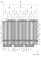
- FIG. 1 is a cross-sectional view of battery 1 according to the present embodiment.
- the battery 1 includes a power generating element 5 , an insulating member 30 , a conductive member 40 , a connecting member 50 , collector terminals 51 and 55 .
- the battery 1 is, for example, an all-solid battery.
- FIG. 2 is a top view of battery 1 according to the present embodiment. 1 shows a cross section taken along line II of FIG.
- the plan view shape of the power generation element 5 is, for example, rectangular as shown in FIG. That is, the shape of the power generation element 5 is a flat rectangular parallelepiped.
- flat means that the thickness (that is, the length in the z-axis direction) is shorter than each side (that is, each length in the x-axis direction and the y-axis direction) or the maximum width of the main surface.
- the plan view shape of the power generation element 5 may be a square, a hexagon, an octagon, or another polygon, or may be a circle, an ellipse, or the like.
- the thickness of each layer is exaggerated in order to facilitate understanding of the layer structure of the power generation element 5 .
- the power generation element 5 includes two main surfaces, a main surface 11 and a main surface 12, as shown in FIGS.
- both main surface 11 and main surface 12 are flat surfaces.
- the main surface 11 is an example of the first main surface.
- Main surface 12 is an example of a second main surface.
- the major surface 11 and the major surface 12 are facing each other and parallel to each other.
- the main surface 11 is the top surface of the power generation element 5 .
- the main surface 12 is the surface opposite to the main surface 11 and is the bottom surface of the power generating element 5 .
- Main surface 11 and main surface 12 each have, for example, a larger area than the side surface of power generation element 5 .
- the side faces of the power generating element 5 include two sets of two parallel side faces facing each other.
- the side surface of the power generation element 5 is, for example, a flat surface.
- the side surface of the power generation element 5 is, for example, a cut surface formed by collectively cutting a stack of a plurality of battery cells 100 . By aligning the cutting direction with the stacking direction, a plurality of battery cells 100 having the same size can be formed.
- the power generation element 5 has multiple battery cells 100 .
- the battery cell 100 is a battery with a minimum configuration and is also called a unit cell.
- a plurality of battery cells 100 are electrically connected in series and stacked.
- all the battery cells 100 included in the power generation element 5 are electrically connected in series.
- a battery 1 is a laminated battery in which a plurality of battery cells 100 are integrated by adhesion, bonding, or the like.
- the number of battery cells 100 included in the power generation element 5 is eight, but the number is not limited to this.
- the number of battery cells 100 included in the power generation element 5 may be an even number such as two or four, or an odd number such as three or five.
- Each of the plurality of battery cells 100 is provided with a through-hole 20 that penetrates each battery cell 100 in the stacking direction.
- the through holes 20 of the plurality of battery cells 100 are collectively formed, for example, by drilling holes penetrating the power generating elements 5 in the stacking direction.
- Each of the plurality of battery cells 100 includes a positive electrode layer 110, a negative electrode layer 120, and a solid electrolyte layer 130.
- the positive electrode layer 110 has a positive electrode current collector 111 and a positive electrode active material layer 112 .
- the negative electrode layer 120 has a negative electrode current collector 121 and a negative electrode active material layer 122 .
- a positive electrode current collector 111, a positive electrode active material layer 112, a solid electrolyte layer 130, a negative electrode active material layer 122, and a negative electrode current collector 121 are stacked in this order along the z-axis. .
- the positive electrode current collector 111, the positive electrode active material layer 112, the solid electrolyte layer 130, the negative electrode active material layer 122, and the negative electrode current collector 121 each extend in a direction perpendicular to the z-axis direction (that is, the x-axis direction and y-axis direction).
- the configurations of the plurality of battery cells 100 are, for example, substantially the same.
- the plurality of battery cells 100 are stacked along the z-axis such that the layers forming the battery cells 100 are arranged in the same order. Thereby, the plurality of battery cells 100 are electrically connected in series and stacked.
- the plurality of battery cells 100 have, for example, the same size. As a result, the operation states of the plurality of battery cells 100 can be easily aligned, and the battery 1 can achieve both high capacity density and high reliability.
- main surface 11 constitutes part of positive electrode layer 110 of battery cell 100 positioned at the top. Specifically, main surface 11 is the upper main surface of positive electrode layer 110 of battery cell 100 positioned at the top.
- main surface 12 constitutes part of the negative electrode layer 120 of the battery cell 100 positioned at the bottom.
- main surface 12 is the lower main surface of negative electrode layer 120 of battery cell 100 positioned at the bottom.
- two battery cells 100 adjacent in the stacking direction share a current collector. That is, one positive electrode current collector 111 of the two battery cells 100 and the other negative electrode current collector 121 of the two battery cells 100 constitute one intermediate layer current collector 140 .
- the positive electrode active material layer 112 is laminated on the lower surface of the intermediate layer current collector 140 .
- a negative electrode active material layer 122 is laminated on the upper surface of the intermediate current collector 140 .
- Interlayer current collector 140 is also referred to as a bipolar current collector.
- the end layer current collectors 150 shown in FIG. 1 are positioned at both ends of the power generation element 5 in the stacking direction.
- a positive electrode active material layer 112 is arranged on the lower surface of the positive electrode current collector 111 .
- the end layer current collector 150 located at the lower end, which is the other end in the stacking direction, is the negative electrode current collector 121 .
- a negative electrode active material layer 122 is arranged on the upper surface of the negative electrode current collector 121 .
- FIG. 3A is a cross-sectional view of battery cell 100 included in power generation element 5 according to the present embodiment.
- the positive electrode current collector 111 and the negative electrode current collector 121 shown in FIG. 3A are the intermediate layer current collector 140 or the end layer current collector 150 shown in FIG. 1, respectively.
- the positive electrode current collector 111 and the negative electrode current collector 121 are conductive foil-like, plate-like, or mesh-like members, respectively.
- the positive electrode current collector 111 and the negative electrode current collector 121 may each be, for example, a conductive thin film. Examples of materials that constitute the positive electrode current collector 111 and the negative electrode current collector 121 include metals such as stainless steel (SUS), aluminum (Al), copper (Cu), and nickel (Ni).
- the positive electrode current collector 111 and the negative electrode current collector 121 may be formed using different materials.
- each of the positive electrode current collector 111 and the negative electrode current collector 121 is, for example, 5 ⁇ m or more and 100 ⁇ m or less, but is not limited to this.
- a cathode active material layer 112 is in contact with the main surface of the cathode current collector 111 .
- the positive electrode current collector 111 may include a current collector layer which is a layer containing a conductive material and provided in a portion in contact with the positive electrode active material layer 112 .
- a negative electrode active material layer 122 is in contact with the main surface of the negative electrode current collector 121 .
- the negative electrode current collector 121 may include a current collector layer which is a layer containing a conductive material and provided in a portion in contact with the negative electrode active material layer 122 .
- intermediate layer current collector 140 and the end layer current collector 150 may have the same thickness and material. Different current collectors, such as thickness and material, may be used.
- the positive electrode active material layer 112 is arranged on the main surface of the positive electrode current collector 111 on the negative electrode layer 120 side.
- the positive electrode active material layer 112 is a layer containing a positive electrode material such as an active material.
- the positive electrode active material layer 112 contains, for example, a positive electrode active material.
- Examples of the positive electrode active material contained in the positive electrode active material layer 112 include lithium cobaltate composite oxide (LCO), lithium nickelate composite oxide (LNO), lithium manganate composite oxide (LMO), and lithium-manganese.
- - Positive electrode active materials such as nickel composite oxide (LMNO), lithium-manganese-cobalt composite oxide (LMCO), lithium-nickel-cobalt composite oxide (LNCO), lithium-nickel-manganese-cobalt composite oxide (LNMCO) substances can be used.
- Various materials capable of withdrawing and inserting ions such as Li or Mg can be used as the material of the positive electrode active material.
- a solid electrolyte such as an inorganic solid electrolyte may be used.
- a sulfide solid electrolyte, an oxide solid electrolyte, or the like can be used as the inorganic solid electrolyte.
- a sulfide solid electrolyte for example, a mixture of Li2S and P2S5 can be used.
- the surface of the positive electrode active material may be coated with a solid electrolyte.
- a conductive material such as acetylene black or a binding binder such as polyvinylidene fluoride may be used.
- the positive electrode active material layer 112 is produced by coating the main surface of the positive electrode current collector 111 with a paste-like paint in which the material contained in the positive electrode active material layer 112 is kneaded together with a solvent and drying it.
- the positive electrode layer 110 also referred to as a positive electrode plate
- the thickness of the positive electrode active material layer 112 is, for example, 5 ⁇ m or more and 300 ⁇ m or less, but is not limited thereto.
- the negative electrode active material layer 122 is arranged on the main surface of the negative electrode current collector 121 on the positive electrode layer 110 side.
- the negative electrode active material layer 122 is arranged to face the positive electrode active material layer 112 .
- the negative electrode active material layer 122 is a layer containing, for example, a negative electrode material such as an active material.
- the negative electrode material is a material that constitutes the counter electrode of the positive electrode material.
- the negative electrode active material layer 122 contains, for example, a negative electrode active material.
- a negative electrode active material contained in the negative electrode active material layer 122 for example, a negative electrode active material such as graphite or metallic lithium can be used.
- Various materials capable of extracting and inserting ions such as lithium (Li) or magnesium (Mg) may be used as materials of the negative electrode active material.
- a solid electrolyte such as an inorganic solid electrolyte may be used.
- an inorganic solid electrolyte for example, a sulfide solid electrolyte or an oxide solid electrolyte can be used.
- a sulfide solid electrolyte for example, a mixture of lithium sulfide (Li 2 S) and phosphorus pentasulfide (P 2 S 5 ) can be used.
- a conductive material such as acetylene black, or a binding binder such as polyvinylidene fluoride may be used.
- the negative electrode active material layer 122 is produced by coating the main surface of the negative electrode current collector 121 with a paste-like paint in which the material contained in the negative electrode active material layer 122 is kneaded together with a solvent and drying it.
- the negative electrode layer 120 also referred to as a negative electrode plate
- the thickness of the negative electrode active material layer 122 is, for example, 5 ⁇ m or more and 300 ⁇ m or less, but is not limited thereto.
- the solid electrolyte layer 130 is arranged between the positive electrode active material layer 112 and the negative electrode active material layer 122 . Solid electrolyte layer 130 is in contact with each of positive electrode active material layer 112 and negative electrode active material layer 122 .
- Solid electrolyte layer 130 is a layer containing an electrolyte material. As the electrolyte material, generally known battery electrolytes can be used. The thickness of solid electrolyte layer 130 may be 5 ⁇ m or more and 300 ⁇ m or less, or may be 5 ⁇ m or more and 100 ⁇ m or less.
- Solid electrolyte layer 130 contains a solid electrolyte.
- the solid electrolyte has, for example, lithium ion conductivity.
- a solid electrolyte such as an inorganic solid electrolyte can be used.
- a sulfide solid electrolyte, an oxide solid electrolyte, or the like can be used as the inorganic solid electrolyte.
- a sulfide solid electrolyte for example, a mixture of Li2S and P2S5 can be used.
- the solid electrolyte layer 130 may contain a binding binder such as polyvinylidene fluoride.
- the positive electrode active material layer 112, the negative electrode active material layer 122, and the solid electrolyte layer 130 are maintained in the form of parallel plates. As a result, it is possible to suppress the occurrence of cracks or collapse due to bending. Note that the positive electrode active material layer 112, the negative electrode active material layer 122, and the solid electrolyte layer 130 may be combined and smoothly curved.
- the end face of the positive electrode current collector 111 and the end face of the negative electrode current collector 121 match when viewed from the z-axis direction.
- positive electrode current collector 111 positive electrode active material layer 112, solid electrolyte layer 130, negative electrode active material layer 122, and negative electrode current collector 121 have the same shape and size. , the contours of each match. That is, the shape of the battery cell 100 is a flat rectangular parallelepiped plate shape.
- the intermediate layer current collector 140 is shared by the plurality of battery cells 100 as shown in FIG.
- Such a power generation element 5 is formed by combining and stacking not only the battery cell 100 shown in FIG. 3A but also the battery cells 100B and 100C shown in FIGS. 3B and 3C.
- the battery cell 100 shown in FIG. 3A will be described as a battery cell 100A.
- a battery cell 100B shown in FIG. 3B has a configuration in which the positive electrode current collector 111 is removed from the battery cell 100A shown in FIG. 3A. That is, the positive electrode layer 110B of the battery cell 100B is composed of the positive electrode active material layer 112 only.
- a battery cell 100C shown in FIG. 3C has a configuration in which the negative electrode current collector 121 is removed from the battery cell 100A shown in FIG. 3A. That is, the negative electrode layer 120C of the battery cell 100C consists of the negative electrode active material layer 122 only.
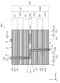
- FIG. 4 is a cross-sectional view showing the power generating element 5 according to this embodiment.
- FIG. 4 is a diagram showing a state before only the power generation element 5 of FIG. 1 is extracted and the through holes 20 are formed in the plurality of battery cells 100 .
- the battery cell 100A is arranged in the bottom layer, and a plurality of battery cells 100C are sequentially stacked upward in the same direction. Thereby, the power generation element 5 is formed.
- the method of forming the power generation element 5 is not limited to this.
- the battery cell 100A may be arranged in the uppermost layer.
- the battery cell 100A may be arranged at a position different from both the top layer and the bottom layer.
- a plurality of battery cells 100A may be used.
- a unit of two battery cells 100 sharing a current collector may be formed by coating both sides of one current collector, and the formed units may be stacked.
- all battery cells 100 are connected in series, and no battery cells connected in parallel are included. Therefore, a high-voltage battery 1 can be realized.
- a through-hole 20 is provided in each of the plurality of battery cells 100 .
- the through hole 20 penetrates from one main surface of the battery cell 100 to the other main surface.
- Through hole 20 extends from one main surface of battery cell 100 to the other main surface through positive electrode layer 110 , solid electrolyte layer 130 and negative electrode layer 120 .
- the cross-sectional area of the through-hole 20 in the direction perpendicular to the stacking direction in the positive electrode layer 110 is the cross-sectional area of the through-hole 20 in the direction perpendicular to the stacking direction in the negative electrode layer 120. larger than area.
- the direction perpendicular to the stacking direction is the extending direction of each layer.
- the width of the through-hole 20 in the positive electrode layer 110 is larger than the width of the through-hole 20 in the negative electrode layer 120 in a cross-sectional view.
- the through holes 20 of the plurality of battery cells 100 are continuous. Thereby, each through-hole 20 of the plurality of battery cells 100 forms one through-hole that penetrates the power generation element 5 in the stacking direction. This makes it easier to form the conductive member 40 and the like extending through the through hole 20 .
- the through hole 20 of the battery cell 100 positioned at the top is open on the main surface 11 .
- the opening position 21 of the through hole 20 of the battery cell 100 positioned at the top is positioned on the main surface 11 .
- the through hole 20 of the battery cell 100 positioned at the bottom is open on the main surface 12 . That is, the opening position 22 of the through hole 20 of the battery cell 100 positioned at the bottom is positioned on the main surface 12 .
- the positive electrode layer 110 is arranged on the main surface 11 side, and the negative electrode layer 120 is arranged on the main surface 12 side.
- the through hole 20 has a shape in which the cross-sectional area on the main surface 12 side in the stacking direction is narrow. Therefore, the opening area of through-hole 20 on main surface 11 is larger than the opening area of through-hole 20 on main surface 12 .
- the collector terminal 51 is positioned inside the through hole 20 in plan view with respect to the main surface 11, as will be described later. By increasing the opening area of the through hole 20 in the main surface 11 , it becomes easier to form the collector terminal 51 provided on the main surface 11 side.
- each through-hole 20 of the plurality of battery cells 100 is inclined with respect to the stacking direction. That is, each through-hole 20 of the plurality of battery cells 100 has a tapered inner wall 25 . This makes it possible to easily provide a difference in the cross-sectional area of the through hole 20 between the positive electrode layer 110 and the negative electrode layer 120 .
- the inner wall 25 is the inner side surface of the battery cell 100 forming the through hole 20 . In this embodiment, the entire surface of the inner wall 25 is inclined with respect to the stacking direction. Note that the inner wall 25 may have a portion that is not inclined with respect to the stacking direction.
- the inner wall 25 is composed of inner surfaces of the positive electrode layer 110 , the solid electrolyte layer 130 and the negative electrode layer 120 , for example.
- each through-hole 20 of the plurality of battery cells 100 has, for example, a truncated cone shape.
- the inner wall 25 of the through hole 20 is not formed with a corner, and electric field concentration inside the through hole 20 can be suppressed.
- the through hole 20 can be easily formed by a drill having a taper angle or the like. Note that.
- the shape of the through hole 20 is not limited to the truncated cone shape, and may be another shape such as a truncated pyramid shape such as a truncated square pyramid shape or a truncated hexagonal pyramid shape.
- the inner wall 25 of each through-hole 20 of the plurality of battery cells 100 forms one continuous surface that is inclined with respect to the stacking direction. Therefore, the through-holes 20 of the plurality of battery cells 100 are continuous to penetrate the power generation element 5 along the stacking direction to form one elongated truncated cone-shaped through-hole. Since the inner walls 25 of the through-holes 20 of the plurality of battery cells 100 are continuous in this way, it is difficult for the inner walls 25 to have easily damaged portions, and the inner walls 25 are less likely to cause the material of the battery cells 100 to collapse. Become. Also, in forming the insulating member 30 and the conductive member 40 , it becomes easier to insert the material into the through hole 20 .
- the direction in which the through holes 20 of the plurality of battery cells 100 are connected may be inclined with respect to the stacking direction.
- the insulating member 30 is arranged inside the through hole 20 .
- the insulating member 30 is positioned between the conductive member 40 and the inner wall 25 of the through hole 20 .
- the insulation member 30 can ensure insulation between the conductive member 40 and the inner surfaces of the plurality of battery cells 100 , which are the inner walls 25 of the through holes 20 .
- the insulating member 30 is arranged along the inner wall 25 of the through hole 20 .
- the insulating member 30 collectively covers the inner walls 25 of the through holes 20 of the plurality of battery cells 100 and is in contact with the inner walls 25 of the through holes 20 of the plurality of battery cells 100 . Thereby, collapse of the material of each layer of the battery cell 100 can be suppressed at the inner wall 25 of the through-hole 20 , and short-circuiting between the positive electrode layer 110 and the negative electrode layer 120 can be suppressed.
- the insulating member 30 covers the entire surface of the inner walls 25 of the through holes 20 of the plurality of battery cells 100 . A gap may be provided in a part between the insulating member 30 and the inner wall 25 .
- the insulating member 30 surrounds the outer periphery of the conductive member 40 when viewed from the stacking direction and is in contact with the conductive member 40 .
- the conductive member 40 is columnar, and the insulating member 30 covers the entire side surface of the columnar conductive member 40 and is in contact with the side surface of the conductive member 40 .
- a gap may be provided in a part between the insulating member 30 and the conductive member 40 .
- the insulating member 30 is filled so as to fill the through holes 20 of the plurality of battery cells 100 together with the conductive member 40 .
- the insulating member 30 for example, completely fills the space between the inner wall 25 of each through-hole 20 of the plurality of battery cells 100 and the conductive member 40 . Therefore, the insulating member 30 has a shape in which the through holes 20 of the plurality of battery cells 100 are connected, except that a through hole through which the conductive member 40 penetrates is formed in the center when viewed in the stacking direction. are the same.
- the shape of the insulating member 30 is, for example, a tubular shape with a circular or polygonal outer periphery.
- the shape of the insulating member 30 is not limited to such a shape, and the insulating member 30 is formed to match the shapes of the through hole 20 and the conductive member 40, for example.
- the thickness of the insulating member 30 increases from the end of the insulating member 30 on the main surface 12 side toward the end of the insulating member 30 on the main surface 11 side. Since the plurality of battery cells 100 are connected in series and stacked, the conductive member 40 electrically connected to the main surface 12 through the through hole 20 and the battery cell at the corresponding position move closer to the main surface 11 . The potential difference with 100 increases. Therefore, the thickness of the insulating member 30 increases in a region where the potential difference between the conductive member 40 and the battery cell 100, that is, the voltage at which the insulating member 30 provides insulation increases. As a result, the insulation reliability is improved, and the reliability of the battery 1 can be improved. In this embodiment, the thickness of insulating member 30 is equal to the distance between conductive member 40 and inner wall 25 . Details of the conductive member 40 will be described later.
- the insulating member 30 is formed using an insulating material that is electrically insulating.
- the insulating member 30 contains resin.
- the resin is, for example, an epoxy resin, but is not limited to this.
- An inorganic material may be used as the insulating material.
- Usable insulating materials are selected based on various properties such as flexibility, gas barrier properties, impact resistance, and heat resistance.
- the insulating member 30 is formed, for example, by filling the through hole 20 with an insulating material, molding the insulating material into the shape of the through hole 20, or coating the inner wall 25 with the insulating material.
- the conductive member 40 is arranged inside the through hole 20 .
- the conductive member 40 is electrically connected to the main surface 12 of the power generating element 5 via the connecting member 50 . Therefore, the conductive member 40 is electrically connected to the end layer current collector 150 in the negative electrode layer 120 of the lowermost battery cell 100 , that is, to the negative electrode current collector 121 .
- the conductive member 40 extends from the opening position 22 of the through hole 20 on the main surface 12 to the opening position 21 of the through hole 20 on the main surface 11 through the through holes 20 of the plurality of battery cells 100 .
- the conductive member 40 penetrates from the main surface 11 to the main surface 12 of the power generation element 5 through the through holes 20 of the plurality of battery cells 100 .
- the potential of the negative electrode layer 120 of the lowermost battery cell 100 is guided to the main surface 11 side, and current can be extracted from the lowermost battery cell 100 on the main surface 11 side of the power generation element 5.
- the conductive member 40 functions as a through electrode penetrating the power generation element 5 . Therefore, in the battery 1, both the positive and negative potentials of the entire power generating element 5 connected in series on the main surface 11 side can be provided.
- the end of the conductive member 40 on the main surface 11 side is in contact with the collector terminal 51 .
- An end portion of the conductive member 40 on the main surface 12 side is in contact with the connecting member 50 .
- An insulating member 30 is arranged between the conductive member 40 and the inner wall 25 .
- the conductive member 40 is formed on the inner wall 25 of the through-hole 20 of each of the plurality of battery cells 100, the positive electrode active material layer 112, the solid electrolyte layer 130, the negative electrode active material layer 122, the intermediate layer current collector 140, and the upper end layer. It is not in contact with the current collector 150 . That is, the conductive member 40 extends from the opening position 22 to the opening position 21 while maintaining insulation from the plurality of battery cells 100 within the through hole 20 .
- the conductive member 40 has, for example, a columnar shape, but may have another shape such as a prismatic shape.
- the thickness of the conductive member 40 is constant, for example.
- the conductive member 40 is formed using a conductive resin material or the like.
- the conductive resin material includes, for example, metal particles and resin.
- the conductive member 40 may be formed using a metal material such as aluminum, copper, nickel, stainless steel, or solder. Conductive materials that can be used are selected based on various properties such as flexibility, gas barrier properties, impact resistance, heat resistance, and solder wettability.
- the conductive member 40 can be formed by methods such as printing, plating, and molding, for example.
- connection member 50 is arranged on the main surface 12 side of the power generation element 5 .
- the connecting member 50 is connected to the conductive member 40 at the opening location 22 .
- the connecting member 50 covers the main surface 12 near the opening position 22 and is also connected to the main surface 12 .
- the connection member 50 electrically connects the conductive member 40 and the main surface 12, that is, the negative electrode layer 120 of the battery cell 100 positioned at the bottom.
- connection member 50 is formed using a conductive material.
- the connection member 50 is formed using metal materials such as aluminum, copper, nickel, stainless steel, and solder.
- the connection member 50 may be formed using a conductive resin material or the like.
- the connection member 50 can be formed by, for example, printing, plating, soldering, or the like.
- the connection member 50 may be formed by connecting the conductive member 40 to the outside of the main surface 12 through the through hole 20 and connecting it to the main surface 12 . In other words, the connecting member 50 may be part of the conductive member 40 .
- the collector terminal 51 is arranged on the main surface 11 side of the power generation element 5 .
- the collector terminal 51 is connected to the conductive member 40 at the opening position 21 .
- the collector terminal 51 is electrically connected to the negative electrode layer 120 of the battery cell 100 positioned at the bottom via the conductive member 40 and the connecting member 50 .
- the current collecting terminal 51 is one of the external connection terminals of the battery 1, and in this embodiment, it is a negative electrode extraction terminal.
- a portion of the collector terminal 51 is in contact with the insulating member 30 . Note that the collector terminal 51 does not have to be in contact with the insulating member 30 .
- the collector terminal 51 may be connected to the conductive member 40 via another conductive connection layer or the like.
- the collector terminal 51 is positioned inside the through-hole 20, in the present embodiment, inside the outer circumference of the insulating member 30 in a plan view with respect to the main surface 11. As shown in FIG. Therefore, the collector terminal 51 is not in contact with the main surface 11 and is insulated from the main surface 11, that is, the positive electrode layer 110 of the battery cell 100 positioned at the top.
- the collector terminal 55 is arranged on the main surface 11 side of the power generation element 5 . Therefore, the collector terminal 51 and the collector terminal 55 are provided on the same main surface 11 side of the power generating element 5 .
- the collector terminal 55 is arranged on the main surface 11 and connected to the main surface 11 . That is, the current collector terminal 55 is electrically connected to the end layer current collector 150 in the positive electrode layer 110 of the uppermost battery cell 100 , ie, the positive electrode current collector 111 .
- the current collecting terminal 55 is one of the external connection terminals of the battery 1, and is a positive electrode extraction terminal in the present embodiment. Note that the collector terminal 55 may be connected to the main surface 11 via another conductive connection layer or the like.
- the collector terminals 51 and 55 are arranged along the x-axis direction, for example.
- the positional relationship between the collector terminal 51 and the collector terminal 55 in plan view is not particularly limited, and is designed according to, for example, the wiring pattern of the board on which the battery 1 is mounted.
- the collector terminal 51 and the collector terminal 55 are protruding terminals provided on the main surface 11 side of the power generating element 5, respectively, but the shape of the collector terminal 51 and the collector terminal 55 is not particularly limited.
- the collector terminal 51 and the collector terminal 55 may extend in a plate shape along the main surface 11 after necessary insulation is performed.
- the collector terminal 51 and the collector terminal 55 are each formed using a material having conductivity.
- the collector terminal 51 and the collector terminal 55 are each formed using a metal material such as aluminum, copper, nickel, stainless steel, or solder.
- each of the current collector terminal 51 and the current collector terminal 55 may be formed using a conductive resin material or the like.
- the collector terminals 51 and the collector terminals 55 can be formed by, for example, printing, plating, soldering, or the like.
- the current collecting terminal 51 may be formed by projecting the conductive member 40 from the through hole 20 to the outside of the main surface 11 . That is, the collector terminal 51 may be part of the conductive member 40 .
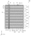
- FIG. 5 is a cross-sectional view showing a usage example of the battery 1. As shown in FIG. FIG. 5 shows the battery 1 mounted on the circuit board 190 in the upside down state of the battery 1 shown in FIG.
- a circuit board 190 for mounting the battery 1 has an insulating plate-like substrate 191 and circuit wiring 192 .
- the circuit wiring 192 is a circuit pattern formed on the substrate 191 .
- the collector terminal 51 of the battery 1 is connected to part of the circuit wiring 192 .
- the collector terminal 55 of the battery 1 is connected to another part of the circuit wiring 192 .
- power from the battery 1 is supplied to the electronic device 195 mounted on the circuit board 190 and connected to the circuit wiring 192 .
- the battery 1 In the battery 1 , current collecting terminals 51 and 55 that are terminals for taking out the positive electrode and the negative electrode are provided on the same main surface 11 . Since the collector terminal 51 and the collector terminal 55 are arranged inside the outer periphery of the power generation element 5 in a plan view, the battery 1 can be mounted on the circuit board 190 with a minimum mounting area and low height.
- the collector terminal 51 and the collector terminal 55 are provided on the main surface 11, the wiring length of the circuit wiring 192 can be easily shortened, and the wiring resistance and the noise caused by the current flowing through the wiring can be reduced. can be reduced.
- circuit board 190 may be mounted with a battery according to each embodiment described later.
- the battery 1 since the plurality of battery cells 100 are connected in series and stacked, the battery 1 with high capacity density and high voltage can be realized.
- a through hole 20 is provided in each of the plurality of battery cells 100 .
- the cross-sectional area of through-hole 20 in the direction perpendicular to the stacking direction in positive electrode layer 110 is larger than the cross-sectional area of through-hole 20 in the direction perpendicular to the stacking direction in negative electrode layer 120 .
- the through holes 20 can reduce the area of the positive electrode layer 110 compared to the negative electrode layer 120 . Therefore, deposition of metal derived from metal ions that have not been taken into the negative electrode layer 120 can be suppressed, and the reliability and safety of the battery 1 can be improved.
- the battery 1 is mounted on a substrate or the like as described above, the battery 1 is replaced infrequently or not in many cases. The significance of sexual improvement is great.
- the battery 1 since the area difference between the positive electrode layer 110 and the negative electrode layer 120 can be realized by the through hole 20, it is necessary to form the battery cell 100 with the area difference between the positive electrode layer 110 and the negative electrode layer 120 in advance. None. Therefore, in the battery 1, for example, by collectively cutting a plurality of stacked battery cells 100, the power generating element 5 having flat side surfaces can be formed. By using batch cutting, for example, the areas of the positive electrode layer 110, the negative electrode layer 120, and the solid electrolyte layer 130 are accurately determined without gradual increase or decrease in film thickness at the coating start and end of each layer. Thereby, the capacity of the battery cell 100 can be utilized to the maximum, and the capacity density of the battery 1 can be increased. In addition, since the capacity variation among the plurality of battery cells 100 is reduced, the accuracy of the battery capacity can be improved.
- the electric potential of the main surface 12 of the power generation element 5, that is, the negative electrode layer 120 of the battery cell 100 located at the bottom, can be led to the main surface 11 side by the conductive member 40 passing through the through hole 20. That is, it is possible to take out the current of both the positive electrode and the negative electrode of the power generation element 5 on the main surface 11 side.
- the mounting of the battery 1 can be made compact.
- the pattern (also referred to as footprint) of connection terminals formed on the substrate can be reduced.
- mounting can be performed in a state in which the main surface 11 of the battery 1 and the substrate are arranged in parallel, so that low-height mounting on the substrate can be realized. Reflow solder connection or the like can be used for mounting. In this way, the battery 1 with excellent mountability can be realized.
- the battery 1 can be miniaturized and the capacity density of the battery 1 can be increased. For example, when mounting the battery 1 on a substrate, it is possible to reduce the mounting area.
- Embodiment 2 Next, Embodiment 2 will be described. The following description focuses on the differences from the first embodiment, and omits or simplifies the description of the common points.
- FIG. 6 is a cross-sectional view of battery 201 according to the present embodiment. As shown in FIG. 6 , battery 201 differs from battery 1 according to Embodiment 1 in that side insulating layer 60 is further provided.
- the side insulating layer 60 covers the side surface of the power generation element 5 .
- the lateral insulation layer 60 covers all sides of the power generation element 5, for example.
- the side insulating layer 60 may cover the respective ends of the main surface 11 and the main surface 12 . As a result, peeling of the end layer current collectors 150 arranged on the main surfaces 11 and 12 can be suppressed, and the reliability of the battery 201 can be further improved.
- the side insulating layer 60 is formed using an electrically insulating insulating material.
- the side insulating layer 60 contains resin.
- the resin is, for example, an epoxy resin, but is not limited to this.
- An inorganic material may be used as the insulating material.
- Usable insulating materials are selected based on various properties such as flexibility, gas barrier properties, impact resistance, and heat resistance.
- side insulating layer 60 may be provided in a battery according to each embodiment described later.
- Embodiment 3 Next, Embodiment 3 will be described. The following description focuses on the differences from the first and second embodiments, and omits or simplifies the description of the common points.
- FIG. 7 is a cross-sectional view of battery 301 according to the present embodiment.
- battery 301 differs from battery 1 according to Embodiment 1 in that battery cell 100 is provided with through hole 320 instead of battery cell 100 with through hole 20 . differ.
- a through hole 320 is provided in each of the plurality of battery cells 100 .
- the cross-sectional area of the through-hole 320 in the direction perpendicular to the stacking direction of the positive electrode layer 110 is the cross-sectional area of the through-hole 320 in the direction perpendicular to the stacking direction of the negative electrode layer 120. larger than area.
- the through holes 320 of the plurality of battery cells 100 have substantially the same volume and shape.
- the inner walls 325 of the through-holes 320 of the plurality of battery cells 100 are inclined at the same angle with respect to the stacking direction.
- the cross-sectional areas of the through-holes 320 in the direction perpendicular to the stacking direction in the positive electrode layers 110 of the plurality of battery cells 100 are substantially the same.
- the cross-sectional area of the through-holes 320 in the direction perpendicular to the stacking direction in the negative electrode layers 120 of the plurality of battery cells 100 is substantially the same.
- the through-holes 320 are formed in each of the plurality of battery cells 100, the volume of the through-holes 320 is the same, so the volumes of the plurality of battery cells 100 are easily uniform, and the capacity variation among the plurality of battery cells 100 is suppressed. can. Therefore, in the charging and discharging of the battery 301, the operating voltage of the plurality of battery cells 100 connected in series and stacked can be easily made uniform, and the occurrence of overcharge or overdischarge in a specific battery cell 100 can be suppressed. Therefore, reliability of the battery 301 can be improved. In particular, in the case of a battery with a small size and a small area, it is effective for the through holes 320 to have the same volume because the effect of the volume of the through holes 320 is large.
- the inner walls 25 of the through holes 20 of the plurality of battery cells 100 form one continuous surface that is inclined with respect to the stacking direction.
- the inner walls 325 of the through-holes 320 of the plurality of battery cells 100 are discontinuous and have a zigzag shape.
- the through holes 320 of the plurality of battery cells 100 are connected to form one through hole penetrating the power generating element 5 in the stacking direction. Also, the insulating member 30 and the conductive member 40 are arranged in the through hole 320 . As a result, the battery 301 with high capacity density, high reliability, and mountability like the battery 1 can be realized.
- Embodiment 4 Next, Embodiment 4 will be described. The following description focuses on the differences from the first to third embodiments, and omits or simplifies the description of the common points.
- FIG. 8 is a cross-sectional view of battery 401 according to the present embodiment.
- battery 401 differs from battery 301 according to Embodiment 3 in that power generation element 405 is provided instead of power generation element 5 .
- Battery 401 also differs from battery 301 according to the third embodiment in that it further includes positive electrode insulating layer 71 , negative electrode insulating layer 72 , negative electrode connection portion 81 , and positive electrode connection portion 82 .
- the power generation element 405 includes multiple battery cells 100 . Some of the plurality of battery cells 100 are electrically connected in parallel and stacked. Power generation element 405 includes both parallel and series connections of battery cells 100 .
- the power generation element 405 includes multiple parallel laminates 407 .
- each of the multiple parallel stacks 407 includes an odd number of battery cells 100, specifically three.
- the odd number of battery cells 100 included in parallel stack 407 are electrically connected in parallel.
- a parallel connection is made by a negative electrode connection portion 81 and a positive electrode connection portion 82 .
- a plurality of parallel laminates 407 are electrically connected in series. The series connection is achieved by stacking the parallel stacks 407 in the stacking direction of the battery cells 100 (that is, the z-axis direction). Specific connections will be described later.
- the number of parallel stacks 407 included in power generation element 405 and the number of battery cells 100 included in parallel stacks 407 are not particularly limited, and may be an odd number or an even number. . Moreover, a stack in which a plurality of battery cells 100 are connected in series may be connected in parallel.
- the power generation element 405 includes side surfaces 13 and 14 . Sides 13 and 14 face away from each other and are parallel to each other. Sides 13 and 14 are each flat surfaces.
- the side surface 13 of the power generation element 405 is formed by connecting the first side surfaces of the plurality of parallel laminates 407 flush with each other.
- the side surface 14 of the power generation element 405 is formed by connecting the second side surfaces of the plurality of parallel laminates 407 flush with each other.
- a large capacity is realized by forming a parallel laminate 407 in which a plurality of battery cells 100 are connected in parallel and laminated. Furthermore, a high voltage is realized by connecting a plurality of parallel laminates 407 in series.
- the layers constituting the battery cells 100 are arranged in reverse order. That is, the plurality of battery cells 100 are stacked side by side along the z-axis while the order of the layers constituting the battery cells 100 alternates.
- the bottom layer and the top layer of parallel stack 407 are current collectors of different polarities, respectively.
- the lowermost layer is the negative electrode current collector 121 of the negative electrode layer 120
- the uppermost layer is the positive electrode current collector 111 of the positive electrode layer 110 .
- Each of the three parallel stacks 407 has the same configuration.
- serial connection can be easily performed by stacking a plurality of parallel stacked bodies 407 in the z-axis direction.
- two parallel laminates 407 can be directly laminated such that current collectors of opposite polarities face each other.
- no insulating layer is arranged between parallel stacked bodies 407 adjacent in the stacking direction. More specifically, in two parallel stacked bodies 407 adjacent to each other, the uppermost positive electrode layer 110 of the lower parallel stacked body 407 and the lowermost negative electrode layer 120 of the upper parallel stacked body 407 share a cell.
- the intermediate layer current collector 141 shown in FIG. 8 is a current collector shared by two parallel laminates 407 .
- the intermediate layer current collector 141 functions as the positive electrode current collector 111 of one parallel laminate 407 and functions as the negative electrode current collector 121 of the other parallel laminate 407 .
- the positive electrode active material layer 112 is arranged on the lower surface of the intermediate current collector 141, and the negative electrode active material layer 122 is arranged on the upper surface.
- each parallel laminate 407 in two adjacent battery cells 100 , two adjacent positive electrode layers 110 share one positive electrode current collector 111 . That is, the positive electrode active material layer 112 is arranged on each of the upper surface and the lower surface of one positive electrode current collector 111 .
- two adjacent negative electrode layers 120 share one negative electrode current collector 121 . That is, the negative electrode active material layer 122 is arranged on each of the upper surface and the lower surface of one negative electrode current collector 121 .
- Such a power generation element 405 can be formed using, for example, battery cells 100A, 100B and 100C shown in FIGS. 3A to 3C.
- the positive electrode insulating layer 71 covers the positive electrode layer 110 on the first side surface of each of the multiple parallel laminates 407 .
- the positive electrode insulating layer 71 includes a plurality of positive electrode layers 110, a plurality of solid electrolyte layers 130, and a plurality of negative electrode active materials included in each of the plurality of parallel laminates 407. a portion of each of the layers 122;
- the positive electrode insulating layer 71 does not cover any of the plurality of negative electrode current collectors 121 included in each of the plurality of parallel stacked bodies 407 on the side surface 13 .
- the positive electrode layers 110 of two adjacent battery cells 100 share one positive electrode current collector 111 , so the positive electrode insulating layer 71 collectively covers the two adjacent positive electrode layers 110 . covering.
- the positive electrode insulating layer 71 is composed of two adjacent battery cells 100, from the negative electrode active material layer 122 of one of the battery cells 100 to the solid electrolyte layer 130, the positive electrode active material layer 112, and the shared positive electrode current collector. 111 , the positive electrode active material layer 112 , the solid electrolyte layer 130 and the negative electrode active material layer 122 of the other battery cell 100 are continuously covered.
- the positive electrode insulating layer 71 covers the solid electrolyte layer 130 and the negative electrode active material layer 122 in addition to the positive electrode layer 110, and thus the width (the length in the z-axis direction) varies due to variations in manufacturing of the positive electrode insulating layer 71.
- the possibility of exposing the positive electrode layer 110 on the side surface 13 is reduced. Therefore, the possibility of contact between the positive electrode layer 110 and the negative electrode connection portion 81 on the side surface 13 to cause a short circuit is reduced, and the reliability of the battery 401 can be improved.
- the positive electrode insulating layer 71 does not have to cover the negative electrode active material layer 122 .
- the positive electrode insulating layer 71 does not have to cover the solid electrolyte layer 130 either.
- the negative electrode insulating layer 72 covers the negative electrode layer 120 on the second side surface of each of the multiple parallel laminates 407 .
- the negative electrode insulating layer 72 includes a plurality of negative electrode layers 120, a plurality of solid electrolyte layers 130, and a plurality of positive electrode active materials included in each of the plurality of parallel laminates 407. a portion of each of the layers 112;
- the negative electrode insulating layer 72 does not cover any of the plurality of positive electrode current collectors 111 included in each of the plurality of parallel stacked bodies 407 on the side surface 14 .
- the positive electrode insulating layer 71 and the negative electrode insulating layer 72 enter into the unevenness of the end faces of the positive electrode active material layer 112, the negative electrode active material layer 122, and the solid electrolyte layer 130, respectively, thereby improving the adhesion strength and improving the reliability of the battery 401. improves.
- the positive electrode active material layer 112, the negative electrode active material layer 122, and the solid electrolyte layer 130 can each be made of a powdery material. In this case, very fine unevenness exists on the end face of each layer.
- the positive electrode insulating layer 71 and the negative electrode insulating layer 72 each have a stripe shape, for example, when the side surface 13 or the side surface 14 is viewed from the front.
- the positive electrode insulating layer 71 and the negative electrode insulating layer 72 are each formed using an electrically insulating insulating material.
- the positive electrode insulating layer 71 and the negative electrode insulating layer 72 each contain resin.
- the resin is, for example, an epoxy resin, but is not limited to this.
- An inorganic material may be used as the insulating material. Usable insulating materials are selected based on various properties such as flexibility, gas barrier properties, impact resistance, and heat resistance.
- the positive electrode insulating layer 71 and the negative electrode insulating layer 72 are formed using the same material, but may be formed using different materials.
- the intermediate layer current collector 141 among all current collectors included in the power generation element 405, the intermediate layer current collector 141, the uppermost positive electrode current collector 111 of the power generation element 405, and the lowermost negative electrode current collector of the power generation element 405 None of the current collectors 121 are covered with an insulating member on each of the side surfaces 13 and 14 . The remaining current collectors included in power generation element 405 are covered with an insulating member on one of side surfaces 13 and 14 .
- the negative electrode connection portion 81 is a conductive portion that covers the first side surface and the positive electrode insulating layer 71 and is connected to the plurality of negative electrode layers 120 in each of the plurality of parallel stacked bodies 407 . That is, the negative electrode connecting portion 81 is provided for each parallel laminated body 407 . As shown in FIG. 8 , three negative electrode connection portions 81 are provided so as to cover side surface 13 . The three negative electrode connection portions 81 are arranged with a predetermined gap therebetween so as not to contact each other.
- the negative electrode connecting portion 81 contacts and covers the end surface of each of the plurality of negative electrode current collectors 121 on the side surface 13 .
- the negative electrode connection portion 81 also contacts and covers at least a portion of each end face of the plurality of negative electrode active material layers 122 . Since the negative electrode connection portion 81 enters the unevenness of the end surface of the negative electrode active material layer 122, the adhesion strength is improved, and the reliability of the battery 401 is improved.
- the positive electrode connecting portion 82 is a conductive portion that covers the second side surface and the negative electrode insulating layer 72 and is connected to the positive electrode layers 110 in each of the plurality of parallel laminates 407 . That is, the positive electrode connection part 82 is provided for each parallel laminate 407 . As shown in FIG. 8, three positive terminal connections 82 are provided to cover the side surface 14 . The three positive electrode connection portions 82 are arranged with a predetermined gap therebetween so as not to contact each other.
- the positive electrode connecting portion 82 contacts and covers the end surface of each of the plurality of positive electrode current collectors 111 on the side surface 14 .
- the positive electrode connecting portion 82 also contacts and covers at least a portion of the end surface of each of the plurality of positive electrode active material layers 112 . Since the positive electrode connection portion 82 enters the unevenness of the end surface of the positive electrode active material layer 112 , the adhesion strength is improved and the reliability of the battery 401 is improved.
- the intermediate layer current collector 141 is both the positive electrode current collector 111 and the negative electrode current collector 121 .
- the intermediate-layer current collector 141 contacts and covers the negative electrode connecting portion 81 on the side surface 13 , and contacts and covers the positive electrode connecting portion 82 on the side surface 14 .
- the negative electrode connection portion 81 that contacts the intermediate layer current collector 141 is connected to the parallel laminate 407 including the intermediate layer current collector 141 as the negative electrode current collector 121 (that is, in the example of FIG. 407) is the negative electrode connection portion 81 of the body 407).
- the negative electrode connection portion 81 of the parallel stacked body 407 on the upper side may be in contact with the positive electrode active material layer 112 of the parallel stacked body 407 on the lower side.
- the positive electrode connection portion 82 that contacts the intermediate layer current collector 141 is a parallel laminate 407 (that is, in the example of FIG. body 407).
- the positive electrode connection portion 82 of the parallel stacked body 407 on the lower side may be in contact with the negative electrode active material layer 122 of the parallel stacked body 407 on the upper side.
- the negative electrode connection portion 81 and the positive electrode connection portion 82 each have a stripe shape, for example, when the side surface 13 or the side surface 14 is viewed from the front.
- the negative electrode connection portion 81 and the positive electrode connection portion 82 are formed using a conductive resin material or the like. Alternatively, the negative electrode connection portion 81 and the positive electrode connection portion 82 may be formed using a metal material such as solder. Conductive materials that can be used are selected based on various properties such as flexibility, gas barrier properties, impact resistance, heat resistance, and solder wettability. The negative electrode connecting portion 81 and the positive electrode connecting portion 82 are formed using the same material, but may be formed using different materials.
- the negative electrode connection part 81 provided on the first side surface of the one parallel stacked body 407 and the positive electrode connection part 82 provided on the second side surface of the one parallel stacked body 407 all the battery cells 100 included in the one parallel stack 407 are connected in parallel.
- Three battery cells 100 are connected in parallel by a negative electrode connection portion 81 and a positive electrode connection portion 82 for each parallel stack 407 . Since the negative electrode connection portion 81 and the positive electrode connection portion 82 can each be realized in a small volume along the side surface 13 or the side surface 14 of the parallel stack 407, the capacity density of the battery 401 can be increased.
- the power generation element 405 includes serial connection and parallel connection of the battery cells 100, a large capacity and high voltage battery 401 can be realized.
- through holes 320 similar to those in Embodiment 3 are formed in each of the plurality of battery cells 100 . Thereby, capacity variation among the plurality of battery cells 100 can be suppressed in the same manner as in the third embodiment.
- the through holes 320 of the plurality of battery cells 100 are connected to form one through hole that penetrates the power generation elements 405 in the stacking direction. Also, the insulating member 30 and the conductive member 40 are arranged in the through hole 320 . As a result, the battery 401 with high capacity density, reliability, and mountability can be realized as in the first embodiment.
- Embodiment 5 Next, Embodiment 5 will be described. The following description focuses on the differences from Embodiments 1 to 4, and omits or simplifies the description of the common points.
- FIG. 9 is a cross-sectional view of battery 501 according to the present embodiment.
- battery 501 differs from battery 1 according to Embodiment 1 in that insulating member 530 and conductive member 540 are provided instead of insulating member 30 and conductive member 40 .
- the insulating member 530 has features similar to those of the insulating member 30, except that the thickness is different from that of the insulating member 30, for example.
- the thickness of the insulating member 530 is constant. Therefore, the surface of the insulating member 530 on the conductive member 540 side is inclined with respect to the stacking direction at the same angle as the inner wall 25 of the through hole 20 . Since the thickness of the insulating member 530 is constant in this way, the options for the material of the insulating member 530 can be increased.
- the insulating member 530 is applied to the inner wall 25 and cured, it can be uniformly cured, and the highly reliable insulating member 530 can be formed. Further, when the insulating member 530 is formed by inserting the insulating member 530 into the through hole 20, the insulating member 530 can be easily inserted.
- the conductive member 540 has the same features as the conductive member 40, except that the shape is, for example, a frustum instead of a columnar shape.
- the shape of the conductive member 540 is, for example, an elongated truncated cone shape, but may be another shape such as an elongated truncated pyramid shape. Since the thickness of the insulating member 530 is constant, the conductive member 540 is formed in a shape that matches the shape of the through hole 20 .
- the conductive member 540 may have a columnar shape, and therefore a gap may be formed between the conductive member 540 and the insulating member 530 .
- Embodiment 6 Next, Embodiment 6 will be described. The following description focuses on the differences from Embodiments 1 to 5, and omits or simplifies the description of the common points.
- FIG. 10 is a cross-sectional view of battery 601 according to the present embodiment.
- battery 601 has power generation element 605 , insulation member 630 and conductive member 640 instead of power generation element 5 , insulating member 30 and conductive member 40 , as compared with battery 1 according to Embodiment 1. It is different in that it has Battery 601 also differs from battery 1 according to Embodiment 1 in that through hole 620 is provided instead of through hole 20 .
- the power generation element 605 includes multiple battery cells 100 and connection layers 160 .
- some of the battery cells 100 form a cell stack 607
- some of the battery cells 100 form a cell stack 608 .
- the battery cells 100 forming the cell stack 607 and the battery cells 100 forming the cell stack 608 do not overlap. It can also be said that the power generation element 605 has a cell stack 607 and a cell stack 608 .
- Cell stack 607 is an example of a first cell stack.
- Cell stack 608 is an example of a second cell stack.
- cell stack 607 and cell stack 608 each include a plurality of battery cells 100, specifically three.
- the number of cell stacks included in power generating element 605 and the number of battery cells 100 included in each of cell stack 607 and cell stack 608 are not particularly limited.
- the number of battery cells 100 forming cell stack 607 may be the same as or different from the number of battery cells 100 forming cell stack 608 .
- the plurality of battery cells 100 included in each of the cell stacks 607 and 608 are electrically connected in series.
- Cell stacks 607 and 608 are electrically connected in series by a conductive member 163 included in connection layer 160 . Therefore, all battery cells 100 of the power generation element 605 are electrically connected in series.
- each of the plurality of battery cells 100 is provided with a through hole 620 that penetrates each battery cell 100 in the stacking direction.
- the cross-sectional area of the through-hole 620 in the direction perpendicular to the stacking direction of the positive electrode layer 110 is the cross-sectional area of the through-hole 620 in the direction perpendicular to the stacking direction of the negative electrode layer 120. larger than area.
- each of cell stack 607 and cell stack 608 a plurality of battery cells 100 are stacked such that through holes 620 are connected.
- Each through-hole 620 of the plurality of battery cells 100 in the cell stack 607 forms one through-hole that penetrates the cell stack 607 .
- each through-hole 620 of the plurality of battery cells 100 in the cell stack 608 forms one through-hole penetrating the cell stack 608 .
- the positions of the through-holes 620 in the cell stack 607 and the through-holes 620 in the cell stack 608 are different when viewed along the stacking direction. As a result, even if the number of stacked battery cells 100 increases and forming the through holes at the same position in all the battery cells 100 causes inconvenience, the positions of the through holes 620 can be changed. . For example, it is possible to avoid difficulty in forming an insulating member or the like in the through-hole due to an increase in the number of battery cells 100 .
- the insulating member 630 is positioned inside the through hole 620 .
- Insulating member 630 is disposed between conductive member 640 and inner wall 625 of through hole 620 .
- the insulating member 630 is divided into, for example, the through-holes 620 of the plurality of battery cells 100 in the cell stack 607 and the through-holes 620 of the plurality of battery cells 100 in the cell stack 608. , have similar features to the insulating member 30 .
- the conductive member 640 is located inside the through hole 620 .
- the conductive member 640 is divided into the through-holes 620 of the plurality of battery cells 100 in the cell stack 607 and the through-holes 620 of the plurality of battery cells 100 in the cell stack 608. , have similar features to the conductive member 40 .
- connection layer 160 is arranged between the cell laminate 607 and the cell laminate 608 .
- Connection layer 160 includes an insulating layer 161 and conductive members 162 and 163 disposed within insulating layer 161 .
- the insulating layer 161 is arranged between the cell stacks 607 and 608 .
- Insulating layer 161 is made of an insulating material and insulates conductive member 640 and conductive member 162 from cell stack 607 and cell stack 608 in connection layer 160 . Also, the insulating layer 161 is arranged between the conductive member 162 and the conductive member 163 .
- the conductive member 162 is embedded in the insulating layer 161 .
- Conductive member 162 is not in contact with conductive member 163 , cell stack 607 and cell stack 608 .
- Conductive member 162 is connected to conductive member 640 disposed within through hole 620 in cell stack 607 and to conductive member 640 disposed within through hole 620 in cell stack 608 . Thereby, the two conductive members 640 are electrically connected. Therefore, in the battery 601 as well, it is possible to take out the current of both the positive electrode and the negative electrode of the power generation element 605 on the main surface 11 side.
- the conductive member 163 is in contact with the positive electrode current collector 111 of the positive electrode layer 110 located at the top of the cell stack 608 and the negative electrode current collector 121 of the negative electrode layer 120 located at the bottom of the cell stack 607 . . Thereby, the cell stack 607 and the cell stack 608 are electrically connected, and all the battery cells 100 of the power generation element 605 are electrically connected in series.
- each of the plurality of battery cells 100 may have the above-described through holes 320 having the same shape in place of the through holes 620 .
- Embodiment 7 Next, Embodiment 7 will be described. The following description focuses on the differences from Embodiments 1 to 6, and omits or simplifies the description of the common points.
- FIG. 11 is a cross-sectional view of battery 701 according to the present embodiment.
- FIG. 12 is a top view of battery 701 according to this embodiment. 11 shows a cross section taken along line XI--XI in FIG.
- battery 701 differs from battery 1 according to Embodiment 1 in that it further includes sealing member 90 .
- the sealing member 90 exposes at least a portion of each of the collector terminals 51 and 55 and seals the power generating element 5 .
- the sealing member 90 is provided, for example, so that the power generating element 5, the insulating member 30, the conductive member 40 and the connecting member 50 are not exposed.
- the sealing member 90 is formed using, for example, an electrically insulating insulating material.
- a generally known battery sealing member material such as a sealing agent can be used.
- a resin material can be used as the insulating material.
- the insulating material may be a material that is insulating and does not have ionic conductivity.
- the insulating material may be at least one of epoxy resin, acrylic resin, polyimide resin, and silsesquioxane.
- the sealing member 90 may contain a plurality of different insulating materials.
- the sealing member 90 may have a multilayer structure. Each layer of the multilayer structure may be formed using different materials and have different properties.
- the sealing member 90 may contain a particulate metal oxide material.
- metal oxide materials silicon oxide, aluminum oxide, titanium oxide, zinc oxide, cerium oxide, iron oxide, tungsten oxide, zirconium oxide, calcium oxide, zeolite, glass, and the like can be used.
- the sealing member 90 may be formed using a resin material in which a plurality of particles made of a metal oxide material are dispersed.
- the particle size of the metal oxide material should be equal to or smaller than the space between the positive electrode current collector 111 and the negative electrode current collector 121 .
- the particle shape of the metal oxide material is, for example, spherical, ellipsoidal, or rod-like, but is not limited thereto.
- the sealing member 90 By providing the sealing member 90, the reliability of the battery 701 can be improved in various aspects such as mechanical strength, short circuit prevention, and moisture resistance.
- batteries according to other embodiments may similarly further include the sealing member 90 .
- the battery 301 according to Embodiment 3 may further include a sealing member 90 like the battery 701a shown in FIG.
- FIG. 13 is a cross-sectional view of battery 701a according to another example of the present embodiment.
- the sealing member 90 exposes at least a portion of each of the current collector terminals 51 and 55, and covers the power generation element 5, the insulating member 30, the conductive member 40, and the connection member 50 so as not to be exposed. ing.
- Embodiment 8 describes a circuit board provided with the battery according to each of the above-described embodiments. The following description focuses on the differences from Embodiments 1 to 7, and omits or simplifies the description of the common points.
- FIG. 14 is a cross-sectional view of the circuit board 2000 according to this embodiment.
- the circuit board 2000 is, for example, a mounting board for mounting the electronic device 195 and the electronic device 196 thereon.
- Electronic device 195 and electronic device 196 are each, for example, a resistor, capacitor, inductor, semiconductor chip, or the like.
- the number of electronic devices mounted on the circuit board 2000 is not particularly limited.
- a circuit board 2000 includes a battery 2001 and a circuit pattern layer 170 .
- the battery 2001 is, for example, the battery 1, 201, 301, 401, 501, 601, 701 or 701a according to the above embodiments.
- FIG. 14 the illustration of the detailed structure of the battery 2001 is omitted for ease of viewing, and only the through hole 20, the insulating member 30, the conductive member 40, the collector terminal 51 and the collector terminal 55 of the battery 2001 are clearly shown.
- FIG. 14 representatively illustrates the through hole 20, the insulating member 30, and the conductive member 40 of the battery 1 according to Embodiment 1.
- a through-hole, an insulating member, and a conductive member of the battery according to 1 may be formed.
- the circuit pattern layer 170 is laminated on the battery 2001 .
- the circuit pattern layer 170 is arranged on the main surface 11 side of the power generation element of the battery 2001 .
- the circuit pattern layer 170 includes a wiring insulating layer 171 and circuit wiring 172 .
- the wiring insulating layer 171 is arranged on the main surface 11 .
- the width (area) of the wiring insulating layer 171 is the same as the width (area) of the battery 2001, but may be smaller or larger than the width (area) of the battery 2001. good.
- a circuit wiring 172 is formed on the surface of the wiring insulating layer 171 opposite to the main surface 11 side.
- the wiring insulating layer 171 is made of an insulating material, and for example, an insulating member for general substrates, such as an insulating film or an insulating plate, can be used. Also, the wiring insulating layer 171 may be a coating layer of an insulating material applied on the battery 2001 . Also, the wiring insulating layer 171 may be part of the sealing member 90 .
- the collector terminals 51 and the collector terminals 55 penetrate the wiring insulating layer 171 and protrude to the opposite side of the wiring insulating layer 171 from the main surface 11 side.
- the circuit wiring 172 is arranged on the side opposite to the main surface 11 side of the wiring insulating layer 171 .
- the circuit wiring 172 is a circuit pattern formed on the wiring insulating layer 171 .
- the circuit wiring 172 is, for example, general printed circuit board wiring. Circuit traces 172 may be conductive patterns formed by other methods.
- An electronic device 195 and an electronic device 196 are connected to the circuit wiring 172 .
- the circuit wiring 172 includes a first wiring 172a and a second wiring 172b.
- the first wiring 172 a is an example of part of the circuit wiring 172 .
- the collector terminal 51 and the collector terminal 55 are connected to the circuit wiring 172 .
- the collector terminal 51 is connected to the first wiring 172a.
- the collector terminal 55 is connected to the second wiring 172b.
- the conductive member 40 is electrically connected to the first wiring 172a via the current collector terminal 51 .
- the main surface 11 is electrically connected to the second wiring 172b through the collector terminal 55.
- the first wiring 172a and the second wiring 172b are separated from each other and are not in contact with each other.
- the collector terminal 51 does not pass through the circuit wiring 172 , and a part of the collector terminal 51 is buried in the circuit wiring 172 .
- the collector terminal 55 penetrates the circuit wiring 172 and the tip of the collector terminal 55 is exposed.
- the positional relationship with the circuit wiring 172 is not particularly limited.
- the collector terminal 51 may pass through the circuit wiring 172 .
- the collector terminal 55 does not have to pass through the circuit wiring 172 .
- At least one of the collector terminal 51 and the collector terminal 55 may be in contact with the main surface 11 side of the circuit wiring 172 at its tip.
- the circuit board 2000 is formed, for example, by separately forming the circuit pattern layer 170 and the battery 2001 and bonding the formed circuit pattern layer 170 and the battery 2001 together.
- the circuit board 2000 may be formed by laminating the insulating layer for wiring 171 on the battery 2001 and patterning the circuit wiring 172 on the laminated insulating layer for wiring 171 .
- the electronic device 195 and the electronic device 196 can be mounted on the circuit pattern layer 170 formed on the battery 2001 .
- the wiring board and the battery are integrated, so that the size and thickness of the electronic device can be reduced.
- the battery 2001 is the battery according to each of the above-described embodiments, both high capacity density and high reliability can be achieved.
- the circuit board 2000 is used for high-frequency equipment that is susceptible to radiation noise.
- the present invention is not limited to this.
- a conductive contact penetrating the wiring insulating layer 171 may be formed to electrically connect the circuit wiring 172 to the conductive member 40 and main surface 11 via the conductive contact.
- FIG. 15 is a flow chart showing Example 1 of the battery manufacturing method according to each embodiment. In the manufacturing method example 1, manufacturing of the battery 1 according to the first embodiment will be mainly described.
- a plurality of battery cells are prepared (step S10).
- the prepared battery cells are, for example, battery cell 100A and battery cell 100B or battery cell 100C shown in FIGS. 3A to 3C. Also, in the following description of the manufacturing method, the battery cells 100A, 100B and 100C may be collectively referred to as the battery cell 100.
- FIG. 1 A block diagram illustrating an exemplary battery cell 100.
- a stack is formed by stacking a plurality of battery cells 100 (step S20).
- a laminate is formed by sequentially stacking a plurality of battery cells 100 such that the positive electrode layer 110, the negative electrode layer 120, and the solid electrolyte layer 130 are arranged in the same order in each battery cell.
- the power generation element 5 shown in FIG. 4 is formed.
- the power generation element 5 is an example of a laminate.
- the side surface of the power generation element 5 may be flattened after stacking the plurality of battery cells 100 .
- the power generating element 5 having flat side surfaces can be formed.
- the cutting process is performed by, for example, a knife, laser or jet.
- through holes 20 are formed in each of the plurality of battery cells 100 so as to penetrate each battery cell 100 in the stacking direction (step S30).
- the cross-sectional area of the through-holes 20 in the direction perpendicular to the stacking direction of the positive electrode layers 110 is the same as that of the through-holes 20 in the direction perpendicular to the stacking direction of the negative electrode layers 120.
- a through-hole 20 is formed so as to have a cross-sectional area larger than that of .
- a through hole 20 as shown in FIG. 1 is formed.
- the through hole 20 is formed by cutting using a drill having a taper angle.
- the through holes 20 may be formed using a laser or the like.
- the through holes 20 are formed after forming the laminate (step S20). Therefore, for example, by forming a through-hole penetrating the power generation element 5 in the stacking direction, the through-hole 20 is collectively formed for each of the plurality of stacked battery cells 100 . In addition, alignment for aligning the through-holes 20 of the plurality of battery cells 100 becomes unnecessary. Therefore, the productivity of manufacturing the battery 1 can be improved. This is particularly effective in the case of manufacturing a large-sized battery 1 in which it is necessary to improve the alignment accuracy of the through holes due to the large area of the power generation element 5 . In addition, the inner walls 25 of the through-holes 20 of the plurality of battery cells 100 can be easily formed into continuous surfaces.
- the insulating member 30 arranged between the inner wall 25 of the through-hole 20 formed in each of the plurality of battery cells 100 and the conductive member 40 is formed (step S40).
- the insulating member 30 is formed to cover the inner wall 25 of the through hole 20 formed in each of the plurality of battery cells 100 .
- the insulating member 30 is formed, for example, within the through hole 20 formed in each of the plurality of battery cells 100, with a space in which the conductive member 40 is formed.
- the insulating member 30 is formed, for example, by applying an insulating material to the inner wall 25 of the through hole 20 .
- the through holes 20 are filled with an insulating material so as to completely fill the through holes 20, and the filled insulating material is filled with a through hole for forming the conductive member 40, that is, having the same shape as the conductive member 40 to be formed.
- the insulating member 30 may be formed by forming a through hole in the .
- a conductive member 40 that passes through the through holes 20 formed in each of the plurality of battery cells 100 and penetrates each of the plurality of battery cells 100 is formed (step S50).
- the conductive member 40 is formed, for example, by filling a space where the insulating member 30 is not formed in the through hole 20 formed in each of the plurality of battery cells 100 with a conductive material. Further, for example, the conductive member 40 may be formed by inserting the conductive member 40 which has been given a shape by molding or the like in advance into the through hole 20 .
- a connection member 50 is formed at the end of the conductive member 40 on the main surface 12 side and at a position where it is connected to the main surface 12 as necessary.
- the formation of the insulating member 30 (step S40) and the formation of the conductive member 40 (step S50) do not have to be performed in this order.
- the formation of the conductive member 40 (step S50) may be performed prior to the formation of the insulating member 30 (step S40).
- the insulating member 30 and the conductive member 40 are separated from each other through the through hole.
- the formation of the insulating member 30 (step S40) and the formation of the conductive member 40 (step S50) may be performed at the same time.
- the insulating member 30 and the conductive member 40 are formed in the through hole 20 by inserting a composite member in which the insulating member 30 and the conductive member 40 are integrated into the through hole 20 .
- a composite member is, for example, a member in which an insulating member 30 is formed around a columnar conductive member 40 .
- the collector terminals 51 and 55 are formed (step S60). Specifically, the collector terminal 51 is formed at a position that is connected to the end of the conductive member 40 on the main surface 11 side and does not contact the main surface 11 . Also, a collector terminal 55 is formed on the main surface 11 .
- the connection member 50, current collector terminals 51, and current collector terminals 55 are formed by disposing a conductive material in desired regions by printing, plating, soldering, or the like.
- the battery 1 shown in FIG. 1 can be manufactured.
- the side insulating layer 60 shown in FIG. 6 may be formed at any timing after the formation of the laminate (step S20).
- the side insulating layer 60 is formed, for example, by applying an insulating material to the side surfaces of the power generation element 5 or the like.
- the side insulating layer 60 may be formed by immersing (dipping) a portion of the power generating element 5 in a liquid insulating material from the side surface side and curing the insulating material adhering to the power generating element 5 . Curing is performed by drying, heating, light irradiation, or the like, depending on the resin material used.
- the sealing member 90 shown in FIGS. 11, 12 and 13 may be formed.
- the sealing member 90 is formed, for example, by coating and curing a resin material having fluidity. Coating is performed by an inkjet method, a spray method, a screen printing method, a gravure printing method, or the like. Curing is performed by drying, heating, light irradiation, or the like, depending on the resin material used.
- FIG. 16 is a flow chart showing Example 2 of the battery manufacturing method according to each embodiment.
- manufacturing method example 2 manufacturing of battery 301 according to the third embodiment will be mainly described.
- Manufacturing method example 2 differs from manufacturing method example 1 in the order of each step.
- step S10 a plurality of battery cells are prepared in the same manner as in Manufacturing Method Example 1 (step S10).
- through-holes 320 are formed in each of the plurality of battery cells 100 so as to penetrate each battery cell 100 in the stacking direction (step S31).
- through holes 320 having the same shape are individually formed in a plurality of battery cells 100 . Since the through-hole 320 can be formed for each battery cell 100 in this way, the through-hole 320 can be easily formed, and the degree of freedom in the shape of the formed through-hole 320 is increased.
- Through-holes having different shapes may be formed in each of the plurality of battery cells 100 .
- the same method as in the manufacturing method example 1 can be used.
- step S21 a stack is formed by stacking a plurality of battery cells 100 (step S21).
- step S21 the plurality of battery cells 100 are stacked so that the through holes 320 formed in each of the plurality of battery cells 100 are connected.
- the insulating member 30 is formed (step S40), the conductive member 40 is formed (step S50), and the collector terminals 51 and 55 are formed (step S60) in the same manner as in Manufacturing Method Example 1. .
- the insulating member 30 and the conductive member 40 can be collectively formed in the through-holes 320 of the plurality of battery cells 100, thereby improving productivity.
- the battery 301 shown in FIG. 7 can be manufactured.
- FIG. 17 is a flow chart showing Example 3 of the battery manufacturing method according to each embodiment.
- manufacturing method example 3 manufacturing of the battery 301 according to the third embodiment will be mainly described.
- Manufacturing method example 3 differs from manufacturing method examples 1 and 2 in the order of each step.
- step S10 a plurality of battery cells are prepared by the same method as manufacturing method example 1 (step S10).
- a through hole 320 is formed in each of the plurality of battery cells 100 in the same manner as in manufacturing method example 2 so as to pass through each battery cell 100 in the stacking direction (step S31).
- the insulating member 30 arranged between the inner wall 325 of the through hole 320 formed in each of the plurality of battery cells 100 and the conductive member 40 is formed (step S42).
- the insulating members 30 are individually formed in the through holes 320 formed in each of the plurality of battery cells 100 .
- a conductive member 40 that passes through the through holes 320 formed in each of the plurality of battery cells 100 and penetrates each of the plurality of battery cells 100 is formed (step S52). Conductive members 40 are individually formed in through-holes 320 formed in each of the plurality of battery cells 100 .
- the same method as in the manufacturing method example 1 can be used.
- the insulating member 30 and the conductive member 40 can be formed for each through-hole 320 before stacking the plurality of battery cells 100, it is easy to insert materials into the through-hole 320, and the insulating member 30 and the conductive member 40 can be easily inserted.
- the conductive member 40 can be formed easily and accurately.
- step S22 a plurality of battery cells 100 are stacked to form a stack.
- the plurality of battery cells 100 are stacked so that the through holes 320 formed in each of the plurality of battery cells 100 are connected.
- the plurality of battery cells 100 are stacked such that the insulating members 30 formed in the through holes 320 of the plurality of battery cells 100 and the conductive members 40 are connected to each other.
- collector terminals 51 and 55 are formed in the same manner as in Manufacturing Method Example 1 (step S60).
- the battery 301 shown in FIG. 7 can be manufactured.
- FIG. 18 is a flow chart showing Example 4 of the battery manufacturing method according to each embodiment.
- manufacturing method example 4 manufacturing of the battery 301 according to the third embodiment will be mainly described.
- Manufacturing method example 4 differs from manufacturing method examples 1 to 3 in the order of each step.
- step S10 a plurality of battery cells are prepared in the same manner as in Manufacturing Method Example 1 (step S10).
- a through hole 320 is formed in each of the plurality of battery cells 100 in the same manner as in manufacturing method example 2 so as to pass through each battery cell 100 in the stacking direction (step S31).
- the insulating member 30 arranged between the inner wall 325 of the through-hole 320 formed in each of the plurality of battery cells 100 and the conductive member 40 is formed by the same method as in Manufacturing Method Example 3 (step S42).
- step S23 a plurality of battery cells 100 are stacked to form a stack.
- the plurality of battery cells 100 are stacked such that the through holes 320 formed in each of the plurality of battery cells 100 are connected.
- the plurality of battery cells 100 are stacked such that the insulating members 30 formed in the through holes 320 of the plurality of battery cells 100 are connected to each other.
- the insulating member 30 has through holes for forming the conductive members 40
- the plurality of battery cells 100 are stacked such that the through holes of the insulating member 30 are connected.
- the through hole 320 is filled with an insulating material so as to completely fill the through hole 320, and a through hole for forming the conductive member 40 is formed in the filled insulating material.
- the insulating member 30 may be formed.
- the formation of the through holes for forming the conductive member 40 may be performed before the formation of the laminate (step S23), and the formation of the plurality of battery cells 100 after the formation of the laminate (step S23). may be performed collectively for
- step S50 the formation of the conductive member 40 (step S50) and the formation of the collector terminals 51 and 55 (step S60) are performed in the same manner as in Manufacturing Method Example 1.
- the battery 301 shown in FIG. 7 can be manufactured.
- one current collector was shared between adjacent battery cells as an intermediate layer current collector, a positive electrode current collector, or a negative electrode current collector. may not be shared.
- Adjacent battery cells may be stacked by bonding two current collectors.
- a negative electrode current collector and a positive electrode current collector may be stacked to form an intermediate layer current collector.
- the battery includes a conductive member and an insulating member, but the present invention is not limited to this. At least one of the conductive member and the insulating member may not be formed in the battery. If the battery does not have a conductive member, the through-hole is used, for example, as a hole for passing a lead wire, a communication wire, or the like, or a hole for fastening with an electronic device.
- the power generation element has a plurality of battery cells, but it is not limited to this.
- the power generation element may be composed of one battery cell.
- the inner wall of the through-hole is inclined with respect to the stacking direction, but the present invention is not limited to this.
- the cross-sectional area of the through-hole in the positive electrode layer may be larger than the cross-sectional area of the through-hole in the negative electrode layer.
- the cross-sectional area of the through hole on the first main surface side is larger than the cross-sectional area of the through hole on the second main surface side, but this is not the only option.
- the stacking order of each layer in each of the plurality of battery cells is reversed up and down, and the positive electrode layer is arranged on the second main surface side, and the cross-sectional area of the through hole on the second main surface side is the cross-sectional area of the through hole on the first main surface side. It is good also as a structure larger than a cross-sectional area.
- external electrodes may be further formed on the collector terminals by plating, printing, soldering, or the like.
- the mountability of the battery can be further improved.
- the insulating member completely fills the space between the conductive member and the inner wall of the through hole, but the present invention is not limited to this.
- the insulating member may cover the inner wall of the through hole and be spaced apart from the conductive member. Further, the insulating member may cover the outer peripheral surface of the conductive member and be separated from the inner wall of the through hole.
- connection relationship of the plurality of battery cells in the power generation element is not limited to the example described in the above embodiment.
- the plurality of battery cells may all be connected in parallel, or any combination of series connection and parallel connection may be used.
- the battery has a collector terminal, but the present invention is not limited to this.
- the battery does not have to have a current collecting terminal.
- a terminal of an electronic device, a contact of a substrate, a pad of a substrate, or the like may be connected to the main surface of the conductive member and the power generating element to draw current from the battery.
- the present disclosure can be used, for example, as batteries or circuit boards for electronic equipment, appliance devices, electric vehicles, and the like.
Landscapes
- Chemical & Material Sciences (AREA)
- Chemical Kinetics & Catalysis (AREA)
- Electrochemistry (AREA)
- General Chemical & Material Sciences (AREA)
- Engineering & Computer Science (AREA)
- Inorganic Chemistry (AREA)
- Manufacturing & Machinery (AREA)
- Composite Materials (AREA)
- Materials Engineering (AREA)
- Physics & Mathematics (AREA)
- Condensed Matter Physics & Semiconductors (AREA)
- General Physics & Mathematics (AREA)
- Connection Of Batteries Or Terminals (AREA)
Abstract
This battery comprises a power generating element that has at least one battery cell that each includes a structure formed by stacking a positive electrode layer, a negative electrode layer, and a solid electrolyte layer located between the positive electrode layer and the negative electrode layer, wherein: a through-hole is provided that penetrates in the stacking direction of each of the at least one battery cell; the cross-sectional area of the through-hole in a direction perpendicular to the stacking direction in the positive electrode layer is greater than the cross-sectional area of the through-hole in a direction perpendicular to the stacking direction in the negative electrode layer; and the inner wall of the through-hole is inclined with respect to the stacking direction.
Description
本開示は、電池、電池の製造方法および回路基板に関する。
The present disclosure relates to a battery, a battery manufacturing method, and a circuit board.
特許文献1には、電池に貫通孔を形成し、貫通孔を利用して配線パターンを設けることが開示されている。
Patent Document 1 discloses forming a through hole in a battery and providing a wiring pattern using the through hole.
特許文献2には、電池に貫通孔を形成し、貫通孔を利用して電池を締結することが開示されている。
Patent Document 2 discloses forming a through hole in a battery and using the through hole to fasten the battery.
従来技術においては、電池を回路に接続して利用する場合に、利便性を高めつつ、信頼性を向上することが望まれている。例えば、電池を基板に実装する場合、電池および他デバイスの実装の更なるバリエーションを増やすなどによって利便性向上を実現しつつ、信頼性を向上することが望まれる。
In the conventional technology, it is desired to improve reliability while increasing convenience when connecting a battery to a circuit and using it. For example, when a battery is mounted on a substrate, it is desirable to improve convenience and improve reliability by increasing variations in the mounting of the battery and other devices.
また、回路に接続される電池においては、容量密度の向上が望まれる。例えば、電池を基板に実装する場合、電池の実装面積を小さくすることは、容量密度を高めるための重要なポイントである。電池の実装面積を小さくするとは、例えば、基板を平面視した場合の電池の発電要素および電池の発電要素から電流を取り出すための端子等の投影面積を小さくすることである。
In addition, it is desirable to improve the capacity density of batteries connected to circuits. For example, when mounting a battery on a substrate, reducing the mounting area of the battery is an important point for increasing the capacity density. To reduce the mounting area of the battery means, for example, to reduce the projected area of the power generation element of the battery and the terminals for extracting current from the power generation element of the battery when the substrate is viewed from above.
そこで、本開示は、高容量密度と高信頼性とを両立できる電池、電池の製造方法および回路基板を提供する。
Therefore, the present disclosure provides a battery, a battery manufacturing method, and a circuit board that can achieve both high capacity density and high reliability.
本開示の一態様に係る電池は、正極層、負極層、および、前記正極層と前記負極層との間に位置する固体電解質層が積層された構造をそれぞれが含む少なくとも1つの電池セルを有する発電要素を備え、前記少なくとも1つの電池セルのそれぞれには、積層方向に貫通する貫通孔が設けられ、前記正極層における積層方向に垂直な方向での前記貫通孔の断面積は、前記負極層における積層方向に垂直な方向での前記貫通孔の断面積よりも大きく、前記貫通孔の内壁は、積層方向に対して傾斜している。
A battery according to an aspect of the present disclosure has at least one battery cell each including a structure in which a positive electrode layer, a negative electrode layer, and a solid electrolyte layer positioned between the positive electrode layer and the negative electrode layer are laminated. Each of the at least one battery cell having a power generation element is provided with a through hole penetrating in the stacking direction, and the cross-sectional area of the through hole in the direction perpendicular to the stacking direction in the positive electrode layer is equal to the negative electrode layer is larger than the cross-sectional area of the through-hole in the direction perpendicular to the stacking direction in , and the inner wall of the through-hole is inclined with respect to the stacking direction.
本開示の一態様に係る電池の製造方法は、複数の電池セルを積層した積層体を形成するステップと、前記複数の電池セルのそれぞれに、積層方向に貫通する貫通孔を形成するステップと、前記複数の電池セルそれぞれに形成された前記貫通孔内を通り、前記複数の電池セルそれぞれを貫通する導電部材を形成するステップと、前記複数の電池セルのそれぞれに形成された前記貫通孔の内壁と前記導電部材との間に配置される絶縁部材を形成するステップと、を含み、前記貫通孔を形成するステップでは、前記正極層における積層方向に垂直な方向での前記貫通孔の断面積が、前記負極層における積層方向に垂直な方向での前記貫通孔の断面積よりも大きくなるように、前記貫通孔を形成する。
A method for manufacturing a battery according to an aspect of the present disclosure includes the steps of: forming a laminate in which a plurality of battery cells are laminated; forming a through hole penetrating in a stacking direction in each of the plurality of battery cells; forming a conductive member that passes through the through-hole formed in each of the plurality of battery cells and penetrates each of the plurality of battery cells; and an inner wall of the through-hole formed in each of the plurality of battery cells. and the step of forming an insulating member disposed between the conductive member and the conductive member, wherein the step of forming the through-hole includes: and forming the through-hole so as to be larger than the cross-sectional area of the through-hole in the direction perpendicular to the stacking direction in the negative electrode layer.
本開示の一態様に係る回路基板は、正極層、負極層、および、前記正極層と前記負極層との間に位置する固体電解質層が積層された構造をそれぞれが含む少なくとも1つの電池セルを有する発電要素と、導電部材と、前記発電要素に積層され、回路配線を有する回路パターン層と、を備え、前記少なくとも1つの電池セルのそれぞれには、積層方向に貫通する貫通孔が設けられ、前記正極層における積層方向に垂直な方向での前記貫通孔の断面積は、前記負極層における積層方向に垂直な方向での前記貫通孔の断面積よりも大きく、前記発電要素では、前記発電要素の第1主面および前記第1主面の反対側の第2主面のそれぞれにおいて、前記少なくとも1つの電池セルのいずれかの前記貫通孔が開口し、前記導電部材は、前記発電要素の第2主面に電気的に接続され、前記第2主面における前記貫通孔の開口位置から、前記貫通孔を通って前記第1主面における前記貫通孔の開口位置まで延び、かつ、前記回路配線の一部と電気的に接続され、前記回路パターン層は、前記発電要素の前記第1主面側に位置する。
A circuit board according to an aspect of the present disclosure includes at least one battery cell each including a structure in which a positive electrode layer, a negative electrode layer, and a solid electrolyte layer positioned between the positive electrode layer and the negative electrode layer are laminated. a power generating element, a conductive member, and a circuit pattern layer laminated on the power generating element and having circuit wiring, and each of the at least one battery cell is provided with a through hole penetrating in the stacking direction, The cross-sectional area of the through-hole in the positive electrode layer in the direction perpendicular to the stacking direction is larger than the cross-sectional area of the through-hole in the negative electrode layer in the direction perpendicular to the stacking direction. and a second main surface opposite to the first main surface, the through hole of any one of the at least one battery cell is open, and the conductive member is connected to the first main surface of the power generation element. The circuit wiring is electrically connected to two main surfaces, extends from the opening position of the through hole on the second main surface through the through hole to the opening position of the through hole on the first main surface, and and the circuit pattern layer is located on the first main surface side of the power generating element.
本開示に係る電池等よれば、高容量密度と高信頼性とを両立できる。
According to the battery or the like according to the present disclosure, both high capacity density and high reliability can be achieved.
(本開示の概要)
本開示の一態様に係る電池は、正極層、負極層、および、前記正極層と前記負極層との間に位置する固体電解質層が積層された構造をそれぞれが含む少なくとも1つの電池セルを有する発電要素を備え、前記少なくとも1つの電池セルのそれぞれには、積層方向に貫通する貫通孔が設けられ、前記正極層における積層方向に垂直な方向での前記貫通孔の断面積は、前記負極層における積層方向に垂直な方向での前記貫通孔の断面積よりも大きく、前記貫通孔の内壁は、積層方向に対して傾斜している。 (Summary of this disclosure)
A battery according to an aspect of the present disclosure has at least one battery cell each including a structure in which a positive electrode layer, a negative electrode layer, and a solid electrolyte layer positioned between the positive electrode layer and the negative electrode layer are laminated. Each of the at least one battery cell having a power generation element is provided with a through hole penetrating in the stacking direction, and the cross-sectional area of the through hole in the direction perpendicular to the stacking direction in the positive electrode layer is equal to the negative electrode layer is larger than the cross-sectional area of the through-hole in the direction perpendicular to the stacking direction in , and the inner wall of the through-hole is inclined with respect to the stacking direction.
これにより、高容量密度と高信頼性とを両立した電池を実現することができる。
As a result, it is possible to realize a battery that achieves both high capacity density and high reliability.
具体的には、正極層における積層方向に垂直な方向での断面積が、負極層における積層方向に垂直な方向での断面積よりも大きい貫通孔によって、負極層よりも正極層の面積を減らすことができる。そのため、負極層に取り込まれなかった金属イオン由来の金属の析出等を抑制でき、電池の信頼性および安全性を高めることができる。
Specifically, the cross-sectional area of the positive electrode layer in the direction perpendicular to the stacking direction is larger than the cross-sectional area of the negative electrode layer in the direction perpendicular to the stacking direction. be able to. Therefore, deposition of metal derived from metal ions that have not been incorporated into the negative electrode layer can be suppressed, and the reliability and safety of the battery can be improved.
また、貫通孔によって、正極層と負極層とに面積差を実現できるため、あらかじめ正極層と負極層とに面積差をつけて電池セルを形成する必要が無い。そのため、例えば、各層の塗工始終端における膜厚の漸増または漸減などがなく、正極層、負極層および固体電解質層の各面積を正確に定めて電池セルを形成できる。これにより、電池セルの容量を最大限に活用できる。また、発電要素から電流の取り出しを行うための導電部材等を貫通孔に通すことができるため、電流の取り出し等のための部材も含めた平面視での面積を小さくすることができる。よって、電池の容量密度を高めることができる。
In addition, since the through-holes can provide a difference in area between the positive electrode layer and the negative electrode layer, there is no need to create a battery cell with a difference in area between the positive electrode layer and the negative electrode layer in advance. Therefore, for example, the thickness of each layer does not gradually increase or decrease at the coating start and end, and the battery cell can be formed by accurately determining the areas of the positive electrode layer, the negative electrode layer, and the solid electrolyte layer. This makes it possible to make the most of the capacity of the battery cells. In addition, since a conductive member or the like for extracting current from the power generation element can be passed through the through hole, the area in plan view including the member for extracting current can be reduced. Therefore, the capacity density of the battery can be increased.
また、例えば、前記発電要素では、前記発電要素の第1主面および前記第1主面の反対側の第2主面のそれぞれにおいて、前記少なくとも1つの電池セルのいずれかの前記貫通孔が開口し、前記電池は、前記発電要素の第2主面に電気的に接続され、前記第2主面における前記貫通孔の開口位置から、前記貫通孔を通って前記第1主面における前記貫通孔の開口位置まで延びる導電部材をさらに備えてもよい。
Further, for example, in the power generation element, the through hole of any one of the at least one battery cell is opened on each of the first main surface and the second main surface opposite to the first main surface of the power generation element. and the battery is electrically connected to the second main surface of the power generation element, and passes through the through hole from the opening position of the through hole on the second main surface to the through hole on the first main surface. It may further comprise a conductive member extending to the opening position of the.
これにより、導電部材によって、発電要素の第2主面の電位を第1主面側に導くことができる。すなわち、発電要素の正極および負極の両方の電流の取り出しが第1主面側で可能になる。これにより、電池の実装をコンパクトにまとめることができる。例えば、基板に形成される接続端子のパターンを小さくすることができる。よって、実装性に優れた電池を実現することができる。また、導電部材が、発電要素内部を通るため、電流の取り出しに必要な構造を発電要素の側面側に形成する必要が無い。そのため、電池を小型化でき、電池の容量密度を高めることができる。例えば、電池を基板に実装する場合、実装面積を小さくすることが可能である。
Thereby, the electric potential of the second main surface of the power generation element can be guided to the first main surface side by the conductive member. That is, it is possible to take out the current of both the positive electrode and the negative electrode of the power generation element on the first main surface side. As a result, the mounting of the battery can be made compact. For example, the pattern of connection terminals formed on the substrate can be made smaller. Therefore, a battery with excellent mountability can be realized. Moreover, since the conductive member passes through the inside of the power generating element, there is no need to form a structure necessary for extracting current on the side surface of the power generating element. Therefore, the size of the battery can be reduced, and the capacity density of the battery can be increased. For example, when mounting a battery on a substrate, it is possible to reduce the mounting area.
また、例えば、前記電池は、前記導電部材と前記貫通孔の内壁との間に位置する絶縁部材をさらに備えてもよい。
Also, for example, the battery may further include an insulating member positioned between the conductive member and the inner wall of the through hole.
これにより、貫通孔の内部で導電部材と電池セルとの絶縁が確保され、電池の信頼性を高めることができる。
As a result, the insulation between the conductive member and the battery cell is ensured inside the through hole, and the reliability of the battery can be improved.
また、例えば、前記絶縁部材は、前記貫通孔の内壁を覆っていてもよい。
Also, for example, the insulating member may cover the inner wall of the through hole.
これにより、貫通孔の内壁において、電池セルの各層の材料の崩落を抑制でき、また、正極層と負極層との短絡を抑制できる。
As a result, collapse of the material of each layer of the battery cell can be suppressed on the inner wall of the through-hole, and short-circuiting between the positive electrode layer and the negative electrode layer can be suppressed.
また、例えば、前記貫通孔は、円錐台形状であってもよい。
Also, for example, the through-hole may have a truncated cone shape.
これにより、貫通孔の内壁に角が形成されず、貫通孔内部での電界集中を抑制できる。
As a result, corners are not formed on the inner wall of the through hole, and electric field concentration inside the through hole can be suppressed.
また、例えば、前記少なくとも1つの電池セルは、複数の電池セルであり、前記複数の電池セルは積層されていてもよい。また、例えば、前記複数の電池セルのうちの少なくとも一部は、電気的に並列接続されて積層されていてもよい。また、例えば、前記複数の電池セルは、電気的に直列接続されて積層されていてもよい。
Also, for example, the at least one battery cell may be a plurality of battery cells, and the plurality of battery cells may be stacked. Further, for example, at least some of the plurality of battery cells may be electrically connected in parallel and stacked. Further, for example, the plurality of battery cells may be electrically connected in series and stacked.
これにより、電池セルが直列接続されて積層された場合には、平面視における面積を変えることなく高電圧の電池を実現できる。また、電池セルが並列接続されて積層された場合には、平面視における面積を変えることなく大容量の電池を実現できる。
As a result, when battery cells are connected in series and stacked, a high-voltage battery can be realized without changing the area in plan view. Also, when battery cells are connected in parallel and stacked, a large-capacity battery can be realized without changing the area in plan view.
また、例えば、前記複数の電池セルのそれぞれの前記貫通孔の体積は同じであってもよい。
Also, for example, the through-holes of the plurality of battery cells may have the same volume.
これにより、複数の電池セルのそれぞれの体積が揃いやすく、複数の電池セル間の容量バラツキを抑制できる。
As a result, the volume of each of the plurality of battery cells can be easily uniformed, and variations in capacity between the plurality of battery cells can be suppressed.
また、例えば、前記複数の電池セルのそれぞれの前記貫通孔の内壁は、積層方向に対して傾斜した連続する面を形成していてもよい。
Also, for example, the inner walls of the through-holes of the plurality of battery cells may form a continuous surface that is inclined with respect to the stacking direction.
これにより、内壁に破損しやすい部分が形成されにくく、内壁で電池セルの材料の崩落等が生じにくくなる。
As a result, it is difficult for the inner wall to have easily damaged parts, and the collapse of the battery cell material on the inner wall is less likely to occur.
また、例えば、前記複数の電池セルのそれぞれの前記貫通孔は連なっていてもよい。
Also, for example, the through-holes of the plurality of battery cells may be continuous.
これにより、貫通孔内に他の部材等を形成しやすくなる。
This makes it easier to form other members inside the through-hole.
また、例えば、前記発電要素では、前記複数の電池セルのうちの一部が、前記貫通孔が連なるように積層されて第1セル積層体を構成し、前記複数の電池セルのうちの他の一部が、前記貫通孔が連なるように積層されて第2セル積層体を構成し、前記第1セル積層体における前記貫通孔と、前記第2セル積層体における前記貫通孔とは、積層方向に沿って見た場合に位置が異なっていてもよい。
Further, for example, in the power generation element, some of the plurality of battery cells are stacked so that the through holes are connected to form a first cell stack, and other of the plurality of battery cells are stacked to form a first cell stack. A part of the cell stack is stacked so that the through holes are connected to form a second cell stack, and the through holes in the first cell stack and the through holes in the second cell stack are arranged in the stacking direction. The position may be different when viewed along the .
これにより、積層される電池セルの数が増えて、全ての電池セルに同じ位置に貫通孔を形成することで不都合が生じる場合でも、貫通孔の位置を変えて形成することができる。例えば、電池セルの数が増えて、貫通孔内に絶縁部材等を形成することが難しくなることを避けることができる。
As a result, even if the number of stacked battery cells increases and forming through-holes in the same position in all the battery cells causes inconvenience, the positions of the through-holes can be changed. For example, it is possible to avoid difficulty in forming an insulating member or the like in the through-hole due to an increase in the number of battery cells.
また、本開示の一態様に係る電池の製造方法は、複数の電池セルを積層した積層体を形成するステップと、前記複数の電池セルのそれぞれに、積層方向に貫通する貫通孔を形成するステップと、前記複数の電池セルそれぞれに形成された前記貫通孔内を通り、前記複数の電池セルそれぞれを貫通する導電部材を形成するステップと、前記複数の電池セルのそれぞれに形成された前記貫通孔の内壁と前記導電部材との間に配置される絶縁部材を形成するステップと、を含み、前記貫通孔を形成するステップでは、前記正極層における積層方向に垂直な方向での前記貫通孔の断面積が、前記負極層における積層方向に垂直な方向での前記貫通孔の断面積よりも大きくなるように、前記貫通孔を形成する。
Further, a method for manufacturing a battery according to an aspect of the present disclosure includes the steps of: forming a laminate in which a plurality of battery cells are laminated; and forming a through hole penetrating in the stacking direction in each of the plurality of battery cells. forming a conductive member that passes through the through-hole formed in each of the plurality of battery cells and penetrates each of the plurality of battery cells; and the through-hole formed in each of the plurality of battery cells. and forming an insulating member disposed between the inner wall of the positive electrode layer and the conductive member, wherein the step of forming the through hole includes cutting the through hole in a direction perpendicular to the stacking direction of the positive electrode layer The through-hole is formed so that the area is larger than the cross-sectional area of the through-hole in the direction perpendicular to the stacking direction in the negative electrode layer.
これにより、上述のような、高容量密度と高信頼性とを両立した、複数の電池セルが積層された電池を製造できる。
As a result, it is possible to manufacture a battery in which a plurality of battery cells are stacked and which achieves both high capacity density and high reliability as described above.
また、これにより、上述のような積層体の一方の主面の電位を他方の主面に導く導電部材、および、貫通孔内で導電部材と電池セルとを絶縁する絶縁部材を備えた電池を形成できる。
In addition, this provides a battery including a conductive member that conducts the potential of one main surface of the laminate as described above to the other main surface, and an insulating member that insulates the conductive member from the battery cell within the through hole. can be formed.
また、例えば、前記積層体を形成するステップの後に、前記貫通孔を形成するステップを行ってもよい。
Further, for example, the step of forming the through holes may be performed after the step of forming the laminate.
これにより、積層された複数の電池セルのそれぞれに一括で貫通孔を形成できるため、電池の生産性が向上する。
As a result, through-holes can be formed in each of the plurality of stacked battery cells all at once, improving the productivity of the battery.
また、例えば、前記積層体を形成するステップでは、前記貫通孔を形成するステップの後に、前記複数の電池セルのそれぞれの前記貫通孔が連なるように前記複数の電池セルを積層し、前記積層体を形成するステップの後に、前記絶縁部材を形成するステップおよび前記導電部材を形成するステップを行ってもよい。
Further, for example, in the step of forming the laminate, after the step of forming the through holes, the plurality of battery cells are laminated such that the through holes of the plurality of battery cells are connected, and the laminate may be followed by forming the insulating member and forming the conductive member.
これにより、電池セルごとに、貫通孔を形成できるため、形成される貫通孔の形状の自由度が高まる。また、積層された電池セルの貫通孔に一括で導電部材および絶縁部材を形成できるため、電池の生産性が向上する。
As a result, a through hole can be formed for each battery cell, increasing the degree of freedom in the shape of the formed through hole. In addition, since the conductive member and the insulating member can be collectively formed in the through-holes of the stacked battery cells, the productivity of the battery is improved.
また、例えば、前記積層体を形成するステップの前に、前記貫通孔を形成するステップ、前記絶縁部材を形成するステップおよび前記導電部材を形成するステップを行ってもよい。
Further, for example, the step of forming the through hole, the step of forming the insulating member, and the step of forming the conductive member may be performed before the step of forming the laminate.
これにより、複数の電池セルのそれぞれの貫通孔ごとに絶縁部材および導電部材を形成できるため、絶縁部材および導電部材を容易に、かつ、精度良く形成できる。
As a result, an insulating member and a conductive member can be formed for each through-hole of a plurality of battery cells, so that the insulating member and the conductive member can be formed easily and accurately.
また、例えば、前記積層体を形成するステップの前に、前記貫通孔を形成するステップおよび前記絶縁部材を形成するステップを行い、前記積層体を形成するステップの後に、前記導電部材を形成するステップを行ってもよい。
Further, for example, the step of forming the through hole and the step of forming the insulating member are performed before the step of forming the laminate, and the step of forming the conductive member is performed after the step of forming the laminate. may be performed.
これにより、電池の信頼性を高めるために精度良く形成することが求められる絶縁部材を容易にかつ精度良く形成できる。また、積層された電池セルの貫通孔に一括で導電部材を形成できるため、電池の生産性が向上する。
As a result, it is possible to easily and accurately form the insulating member, which is required to be formed with high accuracy in order to improve the reliability of the battery. In addition, since the conductive member can be collectively formed in the through-holes of the stacked battery cells, the productivity of the battery is improved.
また、本開示の一態様に係る回路基板は、正極層、負極層、および、前記正極層と前記負極層との間に位置する固体電解質層が積層された構造をそれぞれが含む少なくとも1つの電池セルを有する発電要素と、導電部材と、前記発電要素に積層され、回路配線を有する回路パターン層と、を備え、前記少なくとも1つの電池セルのそれぞれには、積層方向に貫通する貫通孔が設けられ、前記正極層における積層方向に垂直な方向での前記貫通孔の断面積は、前記負極層における積層方向に垂直な方向での前記貫通孔の断面積よりも大きく、前記発電要素では、前記発電要素の第1主面および前記第1主面の反対側の第2主面のそれぞれにおいて、前記少なくとも1つの電池セルのいずれかの前記貫通孔が開口し、前記導電部材は、前記発電要素の第2主面に電気的に接続され、前記第2主面における前記貫通孔の開口位置から、前記貫通孔を通って前記第1主面における前記貫通孔の開口位置まで延び、かつ、前記回路配線の一部と電気的に接続され、前記回路パターン層は、前記発電要素の前記第1主面側に位置する。
Further, a circuit board according to an aspect of the present disclosure includes at least one battery each including a structure in which a positive electrode layer, a negative electrode layer, and a solid electrolyte layer positioned between the positive electrode layer and the negative electrode layer are laminated. A power generation element having cells, a conductive member, and a circuit pattern layer laminated on the power generation element and having circuit wiring, and each of the at least one battery cell is provided with a through hole penetrating in the stacking direction. The cross-sectional area of the through-hole in the positive electrode layer in the direction perpendicular to the stacking direction is larger than the cross-sectional area of the through-hole in the negative electrode layer in the direction perpendicular to the stacking direction, and in the power generation element, the In each of the first main surface and the second main surface opposite to the first main surface of the power generation element, the through hole of any one of the at least one battery cell is open, and the conductive member is provided on the power generation element. is electrically connected to the second main surface of the, extends from the opening position of the through hole on the second main surface through the through hole to the opening position of the through hole on the first main surface, and The circuit pattern layer is electrically connected to part of the circuit wiring and is located on the first main surface side of the power generating element.
これにより、上述の高容量密度と高信頼性とを両立した電池と、当該電池に接続された回路パターン層を備える回路基板が実現される。また、配線基板と電池とが一体化されるので、電子機器の小型化および薄層化を実現できる。また、回路配線の必要な場所に、発電要素から直接電力を供給することができるため、配線の引き回しを削減し、配線からの輻射ノイズを抑制することができる。
As a result, a battery that achieves both high capacity density and high reliability as described above and a circuit board that includes a circuit pattern layer connected to the battery can be realized. In addition, since the wiring board and the battery are integrated, it is possible to reduce the size and thickness of the electronic device. In addition, since power can be directly supplied from the power generation element to a place where circuit wiring is required, it is possible to reduce wiring routing and suppress radiation noise from the wiring.
以下では、実施の形態について、図面を参照しながら具体的に説明する。
Embodiments will be specifically described below with reference to the drawings.
なお、以下で説明する実施の形態は、いずれも包括的または具体的な例を示すものである。以下の実施の形態で示される数値、形状、材料、構成要素、構成要素の配置位置および接続形態、ステップ、ステップの順序などは、一例であり、本開示を限定する主旨ではない。また、以下の実施の形態における構成要素のうち、独立請求項に記載されていない構成要素については、任意の構成要素として説明される。
It should be noted that the embodiments described below are all comprehensive or specific examples. Numerical values, shapes, materials, components, arrangement positions and connection forms of components, steps, order of steps, and the like shown in the following embodiments are examples, and are not intended to limit the present disclosure. Further, among the constituent elements in the following embodiments, constituent elements not described in independent claims will be described as optional constituent elements.
また、各図は、模式図であり、必ずしも厳密に図示されたものではない。したがって、例えば、各図において縮尺などは必ずしも一致しない。また、各図において、実質的に同一の構成については同一の符号を付しており、重複する説明は省略または簡略化する。
In addition, each figure is a schematic diagram and is not necessarily strictly illustrated. Therefore, for example, scales and the like do not necessarily match in each drawing. Moreover, in each figure, substantially the same configurations are denoted by the same reference numerals, and overlapping descriptions are omitted or simplified.
また、本明細書において、平行または直交などの要素間の関係性を示す用語、および、矩形または直方体などの要素の形状を示す用語、ならびに、数値範囲は、厳格な意味のみを表す表現ではなく、実質的に同等な範囲、例えば数%程度の差異をも含むことを意味する表現である。
Also, in this specification, terms that indicate the relationship between elements such as parallel or orthogonal, terms that indicate the shape of elements such as rectangles or cuboids, and numerical ranges are not expressions that express only strict meanings. , is an expression that means that a difference of a substantially equivalent range, for example, a few percent, is also included.
また、本明細書および図面において、x軸、y軸およびz軸は、三次元直交座標系の三軸を示している。x軸およびy軸はそれぞれ、電池の発電要素の平面視形状が矩形である場合に、当該矩形の第一辺、および、当該第一辺に直交する第二辺に平行な方向に一致する。z軸は、発電要素に含まれる複数の電池セルおよび電池セルの各層の積層方向に一致する。
Also, in this specification and drawings, the x-axis, y-axis and z-axis indicate the three axes of a three-dimensional orthogonal coordinate system. The x-axis and the y-axis respectively correspond to the directions parallel to the first side of the rectangle and the second side orthogonal to the first side when the power generating element of the battery has a rectangular plan view shape. The z-axis coincides with the stacking direction of the plurality of battery cells and the layers of the battery cells included in the power generation element.
また、本明細書において、「積層方向」は、集電体および活物質層の主面法線方向に一致する。また、本明細書において、「平面視」とは、単独で使用される場合など、特に断りのない限り、発電要素の主面に対して垂直な方向から見たときのことをいう。なお、「第1側面の平面視」などのように、「ある面の平面視」と記載されている場合は、当該「ある面」を正面から見たときのことをいう。
Also, in this specification, the "stacking direction" corresponds to the direction normal to the main surfaces of the current collector and the active material layer. In this specification, the term “plan view” means when viewed from a direction perpendicular to the main surface of the power generation element, unless otherwise specified, such as when the power generation element is used alone. It should be noted that the term "plan view of a certain surface", such as "plan view of the first side surface", refers to the "certain surface" viewed from the front.
また、本明細書において、「上方」および「下方」という用語は、絶対的な空間認識における上方向(鉛直上方)および下方向(鉛直下方)を指すものではなく、積層構成における積層順を基に相対的な位置関係により規定される用語として用いる。また、「上方」および「下方」という用語は、2つの構成要素が互いに間隔を空けて配置されて2つの構成要素の間に別の構成要素が存在する場合のみならず、2つの構成要素が互いに密着して配置されて2つの構成要素が接する場合にも適用される。以下の説明では、z軸の負側を「下方」または「下側」とし、z軸の正側を「上方」または「上側」とする。
In this specification, the terms “upper” and “lower” do not refer to the upward direction (vertically upward) and the downward direction (vertically downward) in absolute spatial recognition, but are based on the stacking order in the stacking structure. It is used as a term defined by a relative positional relationship. Also, the terms "above" and "below" are used not only when two components are spaced apart from each other and there is another component between the two components, but also when two components are spaced apart from each other. It also applies when two components are in contact with each other and are placed in close contact with each other. In the following description, the negative side of the z-axis is called "lower" or "lower", and the positive side of the z-axis is called "upper" or "upper".
また、本明細書において、「Aを覆う」という表現は、「A」の少なくとも一部を覆うことを意味する。すなわち、「Aを覆う」とは、「Aの全てを覆う」場合だけでなく、「Aの一部のみを覆う」場合も含む表現である。「A」は、例えば、層または端子などの所定の部材の側面および主面などである。
Also, in this specification, the expression "covering A" means covering at least part of "A". That is, the expression "covering A" includes not only the case of "covering all of A" but also the case of "covering only a part of A." "A" is, for example, the side surface and main surface of a given member such as a layer or terminal.
また、本明細書において、「第1」、「第2」などの序数詞は、特に断りのない限り、構成要素の数または順序を意味するものではなく、同種の構成要素の混同を避け、構成要素を区別する目的で用いられている。
In addition, in this specification, ordinal numbers such as “first” and “second” do not mean the number or order of constituent elements unless otherwise specified. It is used for the purpose of distinguishing elements.
(実施の形態1)
以下では、実施の形態1に係る電池の構成について説明する。 (Embodiment 1)
The configuration of the battery according toEmbodiment 1 will be described below.
以下では、実施の形態1に係る電池の構成について説明する。 (Embodiment 1)
The configuration of the battery according to
図1は、本実施の形態に係る電池1の断面図である。図1に示されるように、電池1は、発電要素5と、絶縁部材30と、導電部材40と、接続部材50と、集電端子51と、集電端子55と、を備える。電池1は、例えば全固体電池である。
FIG. 1 is a cross-sectional view of battery 1 according to the present embodiment. As shown in FIG. 1 , the battery 1 includes a power generating element 5 , an insulating member 30 , a conductive member 40 , a connecting member 50 , collector terminals 51 and 55 . The battery 1 is, for example, an all-solid battery.
[1.発電要素]
まず、発電要素5の具体的な構成について、図1および図2を用いて説明する。図2は、本実施の形態に係る電池1の上面図である。なお、図1は、図2のI-I線における断面を表している。 [1. Power generation element]
First, a specific configuration of thepower generation element 5 will be described with reference to FIGS. 1 and 2. FIG. FIG. 2 is a top view of battery 1 according to the present embodiment. 1 shows a cross section taken along line II of FIG.
まず、発電要素5の具体的な構成について、図1および図2を用いて説明する。図2は、本実施の形態に係る電池1の上面図である。なお、図1は、図2のI-I線における断面を表している。 [1. Power generation element]
First, a specific configuration of the
発電要素5の平面視形状は、例えば、図2に示されるように矩形である。つまり、発電要素5の形状は、扁平な直方体である。ここで、扁平とは、厚み(すなわち、z軸方向の長さ)が主面の各辺(すなわち、x軸方向およびy軸方向の各々の長さ)または最大幅より短いことを意味する。発電要素5の平面視形状は、正方形、六角形または八角形などの他の多角形であってもよく、円形または楕円形などであってもよい。なお、図1などの断面図では、発電要素5の層構造を分かりやすくするため、各層の厚みを誇張して図示している。
The plan view shape of the power generation element 5 is, for example, rectangular as shown in FIG. That is, the shape of the power generation element 5 is a flat rectangular parallelepiped. Here, flat means that the thickness (that is, the length in the z-axis direction) is shorter than each side (that is, each length in the x-axis direction and the y-axis direction) or the maximum width of the main surface. The plan view shape of the power generation element 5 may be a square, a hexagon, an octagon, or another polygon, or may be a circle, an ellipse, or the like. In addition, in cross-sectional views such as FIG. 1 , the thickness of each layer is exaggerated in order to facilitate understanding of the layer structure of the power generation element 5 .
発電要素5は、図1および図2に示されるように、2つの主面として、主面11および主面12を含む。本実施の形態では、主面11および主面12はいずれも、平坦面である。
The power generation element 5 includes two main surfaces, a main surface 11 and a main surface 12, as shown in FIGS. In this embodiment, both main surface 11 and main surface 12 are flat surfaces.
主面11は、第1主面の一例である。主面12は、第2主面の一例である。主面11および主面12は、互いに背向しており、かつ、互いに平行である。主面11は、発電要素5の最上面である。主面12は、主面11の反対側の面であり、発電要素5の最下面である。主面11および主面12はそれぞれ、例えば、発電要素5の側面よりも面積が大きい。
The main surface 11 is an example of the first main surface. Main surface 12 is an example of a second main surface. The major surface 11 and the major surface 12 are facing each other and parallel to each other. The main surface 11 is the top surface of the power generation element 5 . The main surface 12 is the surface opposite to the main surface 11 and is the bottom surface of the power generating element 5 . Main surface 11 and main surface 12 each have, for example, a larger area than the side surface of power generation element 5 .
発電要素5の側面は、互いに背向して平行な2つの側面の組を2つ含む。発電要素5の側面は、例えば、平坦面である。発電要素5の側面は、例えば、複数の電池セル100の積層体を一括して切断することにより形成された切断面である。切断方向を積層方向に一致させることで、互いに同じ大きさの複数の電池セル100を形成することができる。
The side faces of the power generating element 5 include two sets of two parallel side faces facing each other. The side surface of the power generation element 5 is, for example, a flat surface. The side surface of the power generation element 5 is, for example, a cut surface formed by collectively cutting a stack of a plurality of battery cells 100 . By aligning the cutting direction with the stacking direction, a plurality of battery cells 100 having the same size can be formed.
図1に示されるように、発電要素5は、複数の電池セル100を有する。電池セル100は、最小構成の電池であり、単位セルとも称される。複数の電池セル100は、電気的に直列接続されて積層されている。これにより、平面視での面積を大きくすることなく高電圧の電池1を実現できる。本実施の形態では、発電要素5が有する全ての電池セル100が電気的に直列接続されている。電池1は、複数の電池セル100が接着または接合などによって一体化された積層電池である。図1に示される例では、発電要素5が有する電池セル100の個数が8個であるが、これに限らない。例えば、発電要素5が有する電池セル100の個数は、2個または4個などの偶数個であってもよく、3個または5個などの奇数個であってもよい。
As shown in FIG. 1, the power generation element 5 has multiple battery cells 100 . The battery cell 100 is a battery with a minimum configuration and is also called a unit cell. A plurality of battery cells 100 are electrically connected in series and stacked. As a result, the high-voltage battery 1 can be realized without increasing the area in plan view. In this embodiment, all the battery cells 100 included in the power generation element 5 are electrically connected in series. A battery 1 is a laminated battery in which a plurality of battery cells 100 are integrated by adhesion, bonding, or the like. In the example shown in FIG. 1, the number of battery cells 100 included in the power generation element 5 is eight, but the number is not limited to this. For example, the number of battery cells 100 included in the power generation element 5 may be an even number such as two or four, or an odd number such as three or five.
複数の電池セル100のそれぞれには、各電池セル100を積層方向に貫通する貫通孔20が設けられている。複数の電池セル100のそれぞれの貫通孔20は、例えば、発電要素5を積層方向に貫通する孔を開けることで、一括で形成される。
Each of the plurality of battery cells 100 is provided with a through-hole 20 that penetrates each battery cell 100 in the stacking direction. The through holes 20 of the plurality of battery cells 100 are collectively formed, for example, by drilling holes penetrating the power generating elements 5 in the stacking direction.
複数の電池セル100のそれぞれは、正極層110と、負極層120と、固体電解質層130と、を含む。正極層110は、正極集電体111と、正極活物質層112と、を有する。負極層120は、負極集電体121と、負極活物質層122と、を有する。複数の電池セル100の各々では、正極集電体111、正極活物質層112、固体電解質層130、負極活物質層122および負極集電体121がこの順でz軸に沿って積層されている。電池セル100の各々では、正極集電体111、正極活物質層112、固体電解質層130、負極活物質層122および負極集電体121はそれぞれ、z軸方向と垂直な方向(つまり、x軸方向およびy軸方向)に延在している。
Each of the plurality of battery cells 100 includes a positive electrode layer 110, a negative electrode layer 120, and a solid electrolyte layer 130. The positive electrode layer 110 has a positive electrode current collector 111 and a positive electrode active material layer 112 . The negative electrode layer 120 has a negative electrode current collector 121 and a negative electrode active material layer 122 . In each of the plurality of battery cells 100, a positive electrode current collector 111, a positive electrode active material layer 112, a solid electrolyte layer 130, a negative electrode active material layer 122, and a negative electrode current collector 121 are stacked in this order along the z-axis. . In each battery cell 100, the positive electrode current collector 111, the positive electrode active material layer 112, the solid electrolyte layer 130, the negative electrode active material layer 122, and the negative electrode current collector 121 each extend in a direction perpendicular to the z-axis direction (that is, the x-axis direction and y-axis direction).
複数の電池セル100の構成は、例えば、互いに実質的に同一である。発電要素5では、電池セル100を構成する各層の並び順が同じになるように、複数の電池セル100は、z軸に沿って並んで積層されている。これにより、複数の電池セル100は、電気的に直列接続されて積層されている。複数の電池セル100は、例えば、互いに同じ大きさである。これにより、複数の電池セル100の動作状態が揃いやすくなり、高容量密度と高信頼性とを両立した電池1を実現できる。
The configurations of the plurality of battery cells 100 are, for example, substantially the same. In the power generating element 5 , the plurality of battery cells 100 are stacked along the z-axis such that the layers forming the battery cells 100 are arranged in the same order. Thereby, the plurality of battery cells 100 are electrically connected in series and stacked. The plurality of battery cells 100 have, for example, the same size. As a result, the operation states of the plurality of battery cells 100 can be easily aligned, and the battery 1 can achieve both high capacity density and high reliability.
本実施の形態においては、主面11は、最上部に位置する電池セル100の正極層110の一部を構成している。具体的には、主面11は、最上部に位置する電池セル100の正極層110の上側の主面である。
In the present embodiment, main surface 11 constitutes part of positive electrode layer 110 of battery cell 100 positioned at the top. Specifically, main surface 11 is the upper main surface of positive electrode layer 110 of battery cell 100 positioned at the top.
また、主面12は、最下部に位置する電池セル100の負極層120の一部を構成している。具体的には、主面12は、最下部に位置する電池セル100の負極層120の下側の主面である。
In addition, the main surface 12 constitutes part of the negative electrode layer 120 of the battery cell 100 positioned at the bottom. Specifically, main surface 12 is the lower main surface of negative electrode layer 120 of battery cell 100 positioned at the bottom.
本実施の形態では、複数の電池セル100のうち、積層方向において隣り合う2つの電池セル100で集電体が共有されている。すなわち、2つの電池セル100の一方の正極集電体111と、2つの電池セル100の他方の負極集電体121とは、1枚の中間層集電体140である。
In the present embodiment, among the plurality of battery cells 100, two battery cells 100 adjacent in the stacking direction share a current collector. That is, one positive electrode current collector 111 of the two battery cells 100 and the other negative electrode current collector 121 of the two battery cells 100 constitute one intermediate layer current collector 140 .
具体的には、中間層集電体140の下面には、正極活物質層112が積層されている。中間層集電体140の上面には、負極活物質層122が積層されている。中間層集電体140は、バイポーラ集電体とも称される。
Specifically, the positive electrode active material layer 112 is laminated on the lower surface of the intermediate layer current collector 140 . A negative electrode active material layer 122 is laminated on the upper surface of the intermediate current collector 140 . Interlayer current collector 140 is also referred to as a bipolar current collector.
図1に示される端部層集電体150は、発電要素5の積層方向における両端に位置している。積層方向における一方端である上端に位置する端部層集電体150は、正極集電体111である。正極集電体111の下面には、正極活物質層112が配置されている。積層方向における他方端である下端に位置する端部層集電体150は、負極集電体121である。負極集電体121の上面には、負極活物質層122が配置されている。
The end layer current collectors 150 shown in FIG. 1 are positioned at both ends of the power generation element 5 in the stacking direction. The end layer current collector 150 positioned at the upper end, which is one end in the stacking direction, is the positive electrode current collector 111 . A positive electrode active material layer 112 is arranged on the lower surface of the positive electrode current collector 111 . The end layer current collector 150 located at the lower end, which is the other end in the stacking direction, is the negative electrode current collector 121 . A negative electrode active material layer 122 is arranged on the upper surface of the negative electrode current collector 121 .
以下では、図3Aを用いて、電池セル100の各層の説明を行う。図3Aは、本実施の形態に係る発電要素5に含まれる電池セル100の断面図である。
Each layer of the battery cell 100 will be described below with reference to FIG. 3A. FIG. 3A is a cross-sectional view of battery cell 100 included in power generation element 5 according to the present embodiment.
図3Aに示される正極集電体111および負極集電体121はそれぞれ、図1に示される中間層集電体140または端部層集電体150である。正極集電体111と負極集電体121とはそれぞれ、導電性を有する箔状、板状または網目状の部材である。正極集電体111と負極集電体121とはそれぞれ、例えば、導電性を有する薄膜であってもよい。正極集電体111と負極集電体121とを構成する材料としては、例えば、ステンレス(SUS)、アルミニウム(Al)、銅(Cu)、ニッケル(Ni)などの金属が用いられうる。正極集電体111と負極集電体121とは、異なる材料を用いて形成されていてもよい。
The positive electrode current collector 111 and the negative electrode current collector 121 shown in FIG. 3A are the intermediate layer current collector 140 or the end layer current collector 150 shown in FIG. 1, respectively. The positive electrode current collector 111 and the negative electrode current collector 121 are conductive foil-like, plate-like, or mesh-like members, respectively. The positive electrode current collector 111 and the negative electrode current collector 121 may each be, for example, a conductive thin film. Examples of materials that constitute the positive electrode current collector 111 and the negative electrode current collector 121 include metals such as stainless steel (SUS), aluminum (Al), copper (Cu), and nickel (Ni). The positive electrode current collector 111 and the negative electrode current collector 121 may be formed using different materials.
正極集電体111および負極集電体121の各々の厚みは、例えば5μm以上100μm以下であるが、これに限らない。正極集電体111の主面には、正極活物質層112が接触している。なお、正極集電体111は、正極活物質層112に接する部分に設けられた、導電材料を含む層である集電体層を含んでもよい。負極集電体121の主面には、負極活物質層122が接触している。なお、負極集電体121は、負極活物質層122に接する部分に設けられた、導電材料を含む層である集電体層を含んでもよい。
The thickness of each of the positive electrode current collector 111 and the negative electrode current collector 121 is, for example, 5 μm or more and 100 μm or less, but is not limited to this. A cathode active material layer 112 is in contact with the main surface of the cathode current collector 111 . Note that the positive electrode current collector 111 may include a current collector layer which is a layer containing a conductive material and provided in a portion in contact with the positive electrode active material layer 112 . A negative electrode active material layer 122 is in contact with the main surface of the negative electrode current collector 121 . Note that the negative electrode current collector 121 may include a current collector layer which is a layer containing a conductive material and provided in a portion in contact with the negative electrode active material layer 122 .
また、中間層集電体140と端部層集電体150とは、同じ厚みおよび材料の集電体が用いられてもよく、強度、接合性および接触する活物質層の性質等に応じて、厚みおよび材料等の異なる集電体が用いられてもよい。
In addition, the intermediate layer current collector 140 and the end layer current collector 150 may have the same thickness and material. Different current collectors, such as thickness and material, may be used.
正極活物質層112は、正極集電体111の、負極層120側の主面に配置されている。正極活物質層112は、例えば活物質などの正極材料を含む層である。正極活物質層112は、例えば、正極活物質を含む。
The positive electrode active material layer 112 is arranged on the main surface of the positive electrode current collector 111 on the negative electrode layer 120 side. The positive electrode active material layer 112 is a layer containing a positive electrode material such as an active material. The positive electrode active material layer 112 contains, for example, a positive electrode active material.
正極活物質層112に含有される正極活物質としては、例えば、コバルト酸リチウム複合酸化物(LCO)、ニッケル酸リチウム複合酸化物(LNO)、マンガン酸リチウム複合酸化物(LMO)、リチウム-マンガン-ニッケル複合酸化物(LMNO)、リチウム-マンガン-コバルト複合酸化物(LMCO)、リチウム-ニッケル-コバルト複合酸化物(LNCO)、リチウム-ニッケル-マンガン-コバルト複合酸化物(LNMCO)などの正極活物質が用いられうる。正極活物質の材料としては、LiまたはMgなどのイオンを離脱および挿入することができる各種材料が用いられうる。
Examples of the positive electrode active material contained in the positive electrode active material layer 112 include lithium cobaltate composite oxide (LCO), lithium nickelate composite oxide (LNO), lithium manganate composite oxide (LMO), and lithium-manganese. - Positive electrode active materials such as nickel composite oxide (LMNO), lithium-manganese-cobalt composite oxide (LMCO), lithium-nickel-cobalt composite oxide (LNCO), lithium-nickel-manganese-cobalt composite oxide (LNMCO) substances can be used. Various materials capable of withdrawing and inserting ions such as Li or Mg can be used as the material of the positive electrode active material.
また、正極活物質層112の含有材料としては、例えば、無機系固体電解質などの固体電解質が用いられてもよい。無機系固体電解質としては、硫化物固体電解質または酸化物固体電解質などが用いられうる。硫化物固体電解質としては、例えば、Li2SおよびP2S5の混合物が用いられうる。正極活物質の表面は、固体電解質でコートされていてもよい。また、正極活物質層112の含有材料としては、例えばアセチレンブラックなどの導電材、または、例えばポリフッ化ビニリデンなどの結着用バインダーなどが用いられてもよい。
As the material contained in the positive electrode active material layer 112, for example, a solid electrolyte such as an inorganic solid electrolyte may be used. A sulfide solid electrolyte, an oxide solid electrolyte, or the like can be used as the inorganic solid electrolyte. As a sulfide solid electrolyte , for example, a mixture of Li2S and P2S5 can be used. The surface of the positive electrode active material may be coated with a solid electrolyte. As the material contained in the positive electrode active material layer 112, a conductive material such as acetylene black or a binding binder such as polyvinylidene fluoride may be used.
正極活物質層112の含有材料を溶媒と共に練り込んだペースト状の塗料を、正極集電体111の主面上に塗工し乾燥させることにより、正極活物質層112が作製される。正極活物質層112の密度を高めるために、乾燥後に、正極活物質層112および正極集電体111を含む正極層110(正極板とも称される)をプレスしておいてもよい。正極活物質層112の厚みは、例えば5μm以上300μm以下であるが、これに限らない。
The positive electrode active material layer 112 is produced by coating the main surface of the positive electrode current collector 111 with a paste-like paint in which the material contained in the positive electrode active material layer 112 is kneaded together with a solvent and drying it. In order to increase the density of the positive electrode active material layer 112, the positive electrode layer 110 (also referred to as a positive electrode plate) including the positive electrode active material layer 112 and the positive electrode current collector 111 may be pressed after drying. The thickness of the positive electrode active material layer 112 is, for example, 5 μm or more and 300 μm or less, but is not limited thereto.
負極活物質層122は、負極集電体121の、正極層110側の主面に配置されている。負極活物質層122は、正極活物質層112に対向して配置されている。負極活物質層122は、例えば活物質などの負極材料を含む層である。負極材料は、正極材料の対極を構成する材料である。負極活物質層122は、例えば、負極活物質を含む。
The negative electrode active material layer 122 is arranged on the main surface of the negative electrode current collector 121 on the positive electrode layer 110 side. The negative electrode active material layer 122 is arranged to face the positive electrode active material layer 112 . The negative electrode active material layer 122 is a layer containing, for example, a negative electrode material such as an active material. The negative electrode material is a material that constitutes the counter electrode of the positive electrode material. The negative electrode active material layer 122 contains, for example, a negative electrode active material.
負極活物質層122に含有される負極活物質としては、例えば、グラファイト、金属リチウムなどの負極活物質が用いられうる。負極活物質の材料としては、リチウム(Li)またはマグネシウム(Mg)などのイオンを離脱および挿入することができる各種材料が用いられうる。
As the negative electrode active material contained in the negative electrode active material layer 122, for example, a negative electrode active material such as graphite or metallic lithium can be used. Various materials capable of extracting and inserting ions such as lithium (Li) or magnesium (Mg) may be used as materials of the negative electrode active material.
また、負極活物質層122の含有材料としては、例えば、無機系固体電解質などの固体電解質が用いられてもよい。無機系固体電解質としては、例えば、硫化物固体電解質または酸化物固体電解質などが用いられうる。硫化物固体電解質としては、例えば、硫化リチウム(Li2S)および五硫化二リン(P2S5)の混合物が用いられうる。また、負極活物質層122の含有材料としては、例えばアセチレンブラックなどの導電材、または、例えばポリフッ化ビニリデンなどの結着用バインダーなどが用いられてもよい。
As the material contained in the negative electrode active material layer 122, for example, a solid electrolyte such as an inorganic solid electrolyte may be used. As the inorganic solid electrolyte, for example, a sulfide solid electrolyte or an oxide solid electrolyte can be used. As a sulfide solid electrolyte, for example, a mixture of lithium sulfide (Li 2 S) and phosphorus pentasulfide (P 2 S 5 ) can be used. As the material contained in the negative electrode active material layer 122, for example, a conductive material such as acetylene black, or a binding binder such as polyvinylidene fluoride may be used.
負極活物質層122の含有材料を溶媒と共に練り込んだペースト状の塗料を、負極集電体121の主面上に塗工し乾燥させることにより、負極活物質層122が作製される。負極活物質層122の密度を高めるために、乾燥後に、負極活物質層122および負極集電体121を含む負極層120(負極板とも称される)をプレスしておいてもよい。負極活物質層122の厚みは、例えば5μm以上300μm以下であるが、これに限らない。
The negative electrode active material layer 122 is produced by coating the main surface of the negative electrode current collector 121 with a paste-like paint in which the material contained in the negative electrode active material layer 122 is kneaded together with a solvent and drying it. In order to increase the density of the negative electrode active material layer 122, the negative electrode layer 120 (also referred to as a negative electrode plate) including the negative electrode active material layer 122 and the negative electrode current collector 121 may be pressed after drying. The thickness of the negative electrode active material layer 122 is, for example, 5 μm or more and 300 μm or less, but is not limited thereto.
固体電解質層130は、正極活物質層112と負極活物質層122との間に配置される。固体電解質層130は、正極活物質層112と負極活物質層122との各々に接する。固体電解質層130は、電解質材料を含む層である。電解質材料としては、一般に公知の電池用の電解質が用いられうる。固体電解質層130の厚みは、5μm以上300μm以下であってもよく、または、5μm以上100μm以下であってもよい。
The solid electrolyte layer 130 is arranged between the positive electrode active material layer 112 and the negative electrode active material layer 122 . Solid electrolyte layer 130 is in contact with each of positive electrode active material layer 112 and negative electrode active material layer 122 . Solid electrolyte layer 130 is a layer containing an electrolyte material. As the electrolyte material, generally known battery electrolytes can be used. The thickness of solid electrolyte layer 130 may be 5 μm or more and 300 μm or less, or may be 5 μm or more and 100 μm or less.
固体電解質層130は、固体電解質を含んでいる。固体電解質は、例えば、リチウムイオン伝導性を有する。固体電解質としては、例えば、無機系固体電解質などの固体電解質が用いられうる。無機系固体電解質としては、硫化物固体電解質または酸化物固体電解質などが用いられうる。硫化物固体電解質としては、例えば、Li2SおよびP2S5の混合物が用いられうる。なお、固体電解質層130は、電解質材料に加えて、例えばポリフッ化ビニリデンなどの結着用バインダーなどを含有してもよい。
Solid electrolyte layer 130 contains a solid electrolyte. The solid electrolyte has, for example, lithium ion conductivity. As the solid electrolyte, for example, a solid electrolyte such as an inorganic solid electrolyte can be used. A sulfide solid electrolyte, an oxide solid electrolyte, or the like can be used as the inorganic solid electrolyte. As a sulfide solid electrolyte , for example, a mixture of Li2S and P2S5 can be used. In addition to the electrolyte material, the solid electrolyte layer 130 may contain a binding binder such as polyvinylidene fluoride.
本実施の形態では、正極活物質層112、負極活物質層122、固体電解質層130は平行平板状に維持されている。これにより、湾曲による割れまたは崩落の発生を抑制することができる。なお、正極活物質層112、負極活物質層122、固体電解質層130を合わせて滑らかに湾曲させてもよい。
In the present embodiment, the positive electrode active material layer 112, the negative electrode active material layer 122, and the solid electrolyte layer 130 are maintained in the form of parallel plates. As a result, it is possible to suppress the occurrence of cracks or collapse due to bending. Note that the positive electrode active material layer 112, the negative electrode active material layer 122, and the solid electrolyte layer 130 may be combined and smoothly curved.
また、本実施の形態では、正極集電体111の端面と負極集電体121の端面とは、z軸方向から見た場合に一致している。
In addition, in the present embodiment, the end face of the positive electrode current collector 111 and the end face of the negative electrode current collector 121 match when viewed from the z-axis direction.
より具体的には、電池セル100では、正極集電体111、正極活物質層112、固体電解質層130、負極活物質層122および負極集電体121の各々の形状および大きさが同じであり、各々の輪郭が一致している。つまり、電池セル100の形状は、扁平な直方体状の平板形状である。
More specifically, in battery cell 100, positive electrode current collector 111, positive electrode active material layer 112, solid electrolyte layer 130, negative electrode active material layer 122, and negative electrode current collector 121 have the same shape and size. , the contours of each match. That is, the shape of the battery cell 100 is a flat rectangular parallelepiped plate shape.
上述したように、本実施の形態に係る発電要素5では、図1に示されるように、複数の電池セル100において、中間層集電体140が共有されている。このような発電要素5は、図3Aに示される電池セル100だけでなく、図3Bおよび図3Cに示される電池セル100Bおよび100Cを組み合わせて積層することで形成される。なお、ここでは、図3Aに示される電池セル100を電池セル100Aとして説明する。
As described above, in the power generating element 5 according to the present embodiment, the intermediate layer current collector 140 is shared by the plurality of battery cells 100 as shown in FIG. Such a power generation element 5 is formed by combining and stacking not only the battery cell 100 shown in FIG. 3A but also the battery cells 100B and 100C shown in FIGS. 3B and 3C. Here, the battery cell 100 shown in FIG. 3A will be described as a battery cell 100A.
図3Bに示される電池セル100Bは、図3Aに示される電池セル100Aから正極集電体111を除いた構成を有する。つまり、電池セル100Bの正極層110Bは、正極活物質層112のみからなる。
A battery cell 100B shown in FIG. 3B has a configuration in which the positive electrode current collector 111 is removed from the battery cell 100A shown in FIG. 3A. That is, the positive electrode layer 110B of the battery cell 100B is composed of the positive electrode active material layer 112 only.
図3Cに示される電池セル100Cは、図3Aに示される電池セル100Aから負極集電体121を除いた構成を有する。つまり、電池セル100Cの負極層120Cは、負極活物質層122のみからなる。
A battery cell 100C shown in FIG. 3C has a configuration in which the negative electrode current collector 121 is removed from the battery cell 100A shown in FIG. 3A. That is, the negative electrode layer 120C of the battery cell 100C consists of the negative electrode active material layer 122 only.
図4は、本実施の形態に係る発電要素5を示す断面図である。図4は、図1の発電要素5のみが抜き出され、複数の電池セル100に貫通孔20が形成される前の状態を示す図である。図4に示されるように、最下層に電池セル100Aを配置し、上方に向かって複数の電池セル100Cを同じ向きで順に積層する。これにより、発電要素5が形成される。
FIG. 4 is a cross-sectional view showing the power generating element 5 according to this embodiment. FIG. 4 is a diagram showing a state before only the power generation element 5 of FIG. 1 is extracted and the through holes 20 are formed in the plurality of battery cells 100 . As shown in FIG. 4, the battery cell 100A is arranged in the bottom layer, and a plurality of battery cells 100C are sequentially stacked upward in the same direction. Thereby, the power generation element 5 is formed.
なお、発電要素5を形成する方法は、これに限定されない。例えば、複数の電池セル100Bを同じ向きで順に積層した後、電池セル100Aを最上層に配置してもよい。また、例えば、電池セル100Aを最上層および最下層のいずれとも異なる位置に配置してもよい。また、複数の電池セル100Aを用いてもよい。また、1枚の集電体に対して両面塗工を行うことにより、集電体を共有する2つの電池セル100のユニットを形成し、形成したユニットを積層してもよい。
The method of forming the power generation element 5 is not limited to this. For example, after stacking a plurality of battery cells 100B in order in the same direction, the battery cell 100A may be arranged in the uppermost layer. Also, for example, the battery cell 100A may be arranged at a position different from both the top layer and the bottom layer. Also, a plurality of battery cells 100A may be used. Alternatively, a unit of two battery cells 100 sharing a current collector may be formed by coating both sides of one current collector, and the formed units may be stacked.
以上のように、本実施の形態に係る発電要素5では、全ての電池セル100が直列接続されており、並列接続された電池セルが含まれていない。このため、高電圧の電池1を実現することができる。
As described above, in the power generation element 5 according to the present embodiment, all battery cells 100 are connected in series, and no battery cells connected in parallel are included. Therefore, a high-voltage battery 1 can be realized.
[2.貫通孔]
次に、再び、図1および図2を参照して、貫通孔20について説明する。 [2. through hole]
Next, the throughhole 20 will be described with reference to FIGS. 1 and 2 again.
次に、再び、図1および図2を参照して、貫通孔20について説明する。 [2. through hole]
Next, the through
貫通孔20は、複数の電池セル100のそれぞれに設けられている。複数の電池セル100のそれぞれにおいて、貫通孔20は、電池セル100の一方の主面から他方の主面までを貫通する。貫通孔20は、正極層110、固体電解質層130および負極層120を通って電池セル100の一方の主面から他方の主面に至っている。
A through-hole 20 is provided in each of the plurality of battery cells 100 . In each of the plurality of battery cells 100, the through hole 20 penetrates from one main surface of the battery cell 100 to the other main surface. Through hole 20 extends from one main surface of battery cell 100 to the other main surface through positive electrode layer 110 , solid electrolyte layer 130 and negative electrode layer 120 .
複数の電池セル100のそれぞれの貫通孔20において、正極層110における積層方向に垂直な方向での貫通孔20の断面積は、負極層120における積層方向に垂直な方向での貫通孔20の断面積よりも大きい。積層方向に垂直な方向は、各層の延在方向である。これにより、正極活物質層112における負極活物質層122側の主面の位置での貫通孔20の断面積が大きくなり、その分、正極活物質層112の当該主面の面積が小さくなる。そのため、負極層120に取り込まれなかった金属イオン由来の金属(いわゆるデンドライト)の析出等を抑制でき、電池1の信頼性および安全性を高めることができる。
In each through-hole 20 of the plurality of battery cells 100, the cross-sectional area of the through-hole 20 in the direction perpendicular to the stacking direction in the positive electrode layer 110 is the cross-sectional area of the through-hole 20 in the direction perpendicular to the stacking direction in the negative electrode layer 120. larger than area. The direction perpendicular to the stacking direction is the extending direction of each layer. As a result, the cross-sectional area of the through hole 20 at the position of the main surface of the positive electrode active material layer 112 on the negative electrode active material layer 122 side is increased, and the area of the main surface of the positive electrode active material layer 112 is reduced accordingly. Therefore, deposition of metal derived from metal ions not incorporated into the negative electrode layer 120 (so-called dendrites) can be suppressed, and the reliability and safety of the battery 1 can be enhanced.
複数の電池セル100のそれぞれの貫通孔20において、断面視で、正極層110における貫通孔20の幅は、負極層120における貫通孔20の幅よりも大きい。
In each through-hole 20 of the plurality of battery cells 100, the width of the through-hole 20 in the positive electrode layer 110 is larger than the width of the through-hole 20 in the negative electrode layer 120 in a cross-sectional view.
複数の電池セル100のそれぞれの貫通孔20は連なっている。これにより、複数の電池セル100のそれぞれの貫通孔20は、発電要素5を積層方向に貫通する1つの貫通孔を形成している。これにより、貫通孔20を通って延びる導電部材40等を形成しやすくなる。
The through holes 20 of the plurality of battery cells 100 are continuous. Thereby, each through-hole 20 of the plurality of battery cells 100 forms one through-hole that penetrates the power generation element 5 in the stacking direction. This makes it easier to form the conductive member 40 and the like extending through the through hole 20 .
発電要素5では、主面11において、最上部に位置する電池セル100の貫通孔20が開口している。つまり、最上部に位置する電池セル100の貫通孔20の開口位置21は、主面11に位置する。また、発電要素5では、主面12において、最下部に位置する電池セル100の貫通孔20が開口している。つまり、最下部に位置する電池セル100の貫通孔20の開口位置22は、主面12に位置する。
In the power generation element 5 , the through hole 20 of the battery cell 100 positioned at the top is open on the main surface 11 . In other words, the opening position 21 of the through hole 20 of the battery cell 100 positioned at the top is positioned on the main surface 11 . Moreover, in the power generation element 5 , the through hole 20 of the battery cell 100 positioned at the bottom is open on the main surface 12 . That is, the opening position 22 of the through hole 20 of the battery cell 100 positioned at the bottom is positioned on the main surface 12 .
本実施の形態においては、複数の電池セル100のそれぞれにおいて、正極層110が主面11側に配置され、負極層120が主面12側に配置されている。貫通孔20は、積層方向における主面12側の断面積が狭くなる形状である。そのため、主面11における貫通孔20の開口面積は、主面12における貫通孔20の開口面積よりも大きい。集電端子51は、後述するように、主面11に対する平面視において貫通孔20の内側に位置する。主面11における貫通孔20の開口面積が大きくなることで、主面11側に設けられる集電端子51を形成しやすくなる。
In the present embodiment, in each of the plurality of battery cells 100, the positive electrode layer 110 is arranged on the main surface 11 side, and the negative electrode layer 120 is arranged on the main surface 12 side. The through hole 20 has a shape in which the cross-sectional area on the main surface 12 side in the stacking direction is narrow. Therefore, the opening area of through-hole 20 on main surface 11 is larger than the opening area of through-hole 20 on main surface 12 . The collector terminal 51 is positioned inside the through hole 20 in plan view with respect to the main surface 11, as will be described later. By increasing the opening area of the through hole 20 in the main surface 11 , it becomes easier to form the collector terminal 51 provided on the main surface 11 side.
複数の電池セル100のそれぞれの貫通孔20の内壁25は、積層方向に対して傾斜している。つまり、複数の電池セル100のそれぞれの貫通孔20は、テーパ状の内壁25を有する。これにより、容易に正極層110および負極層120における貫通孔20の断面積に差を設けることができる。内壁25は、貫通孔20を構成する電池セル100の内側面である。本実施の形態では、内壁25の全面が積層方向に対して傾斜している。なお、内壁25のうち、積層方向に対して傾斜していない部分があってもよい。内壁25は、例えば、正極層110、固体電解質層130および負極層120の内側面で構成されている。
The inner wall 25 of each through-hole 20 of the plurality of battery cells 100 is inclined with respect to the stacking direction. That is, each through-hole 20 of the plurality of battery cells 100 has a tapered inner wall 25 . This makes it possible to easily provide a difference in the cross-sectional area of the through hole 20 between the positive electrode layer 110 and the negative electrode layer 120 . The inner wall 25 is the inner side surface of the battery cell 100 forming the through hole 20 . In this embodiment, the entire surface of the inner wall 25 is inclined with respect to the stacking direction. Note that the inner wall 25 may have a portion that is not inclined with respect to the stacking direction. The inner wall 25 is composed of inner surfaces of the positive electrode layer 110 , the solid electrolyte layer 130 and the negative electrode layer 120 , for example.
また、複数の電池セル100のそれぞれの貫通孔20は、例えば、円錐台形状である。これにより、貫通孔20の内壁25に角が形成されず、貫通孔20内部での電界集中を抑制できる。また、テーパ角を有するドリル等によって、容易に貫通孔20を形成できる。なお。貫通孔20の形状は、円錐台形状に限らず、四角錘台形状または六角錘台形状等の角錐台形状等、他の形状であってもよい。
Also, each through-hole 20 of the plurality of battery cells 100 has, for example, a truncated cone shape. As a result, the inner wall 25 of the through hole 20 is not formed with a corner, and electric field concentration inside the through hole 20 can be suppressed. Further, the through hole 20 can be easily formed by a drill having a taper angle or the like. note that. The shape of the through hole 20 is not limited to the truncated cone shape, and may be another shape such as a truncated pyramid shape such as a truncated square pyramid shape or a truncated hexagonal pyramid shape.
複数の電池セル100のそれぞれの貫通孔20の内壁25は、積層方向に対して傾斜した連続する1つの面を形成している。そのため、複数の電池セル100のそれぞれの貫通孔20は、積層方向に沿って発電要素5を貫通するように連なって、1つの長尺状の円錐台形状の貫通孔を形成している。このように、複数の電池セル100のそれぞれの貫通孔20の内壁25が連続することで、内壁25に破損しやすい部分が形成されにくく、内壁25で電池セル100の材料の崩落等が生じにくくなる。また、絶縁部材30および導電部材40の形成において、材料を貫通孔20内に挿入しやすくなる。なお、複数の電池セル100のそれぞれの貫通孔20が連なる方向は、積層方向に対して傾斜していてもよい。
The inner wall 25 of each through-hole 20 of the plurality of battery cells 100 forms one continuous surface that is inclined with respect to the stacking direction. Therefore, the through-holes 20 of the plurality of battery cells 100 are continuous to penetrate the power generation element 5 along the stacking direction to form one elongated truncated cone-shaped through-hole. Since the inner walls 25 of the through-holes 20 of the plurality of battery cells 100 are continuous in this way, it is difficult for the inner walls 25 to have easily damaged portions, and the inner walls 25 are less likely to cause the material of the battery cells 100 to collapse. Become. Also, in forming the insulating member 30 and the conductive member 40 , it becomes easier to insert the material into the through hole 20 . The direction in which the through holes 20 of the plurality of battery cells 100 are connected may be inclined with respect to the stacking direction.
[3.絶縁部材]
次に、絶縁部材30について説明する。 [3. Insulating material]
Next, the insulatingmember 30 will be described.
次に、絶縁部材30について説明する。 [3. Insulating material]
Next, the insulating
絶縁部材30は、貫通孔20内に配置される。絶縁部材30は、導電部材40と貫通孔20の内壁25との間に位置する。絶縁部材30によって、導電部材40と貫通孔20の内壁25である複数の電池セル100それぞれの内側面との絶縁を確保することができる。
The insulating member 30 is arranged inside the through hole 20 . The insulating member 30 is positioned between the conductive member 40 and the inner wall 25 of the through hole 20 . The insulation member 30 can ensure insulation between the conductive member 40 and the inner surfaces of the plurality of battery cells 100 , which are the inner walls 25 of the through holes 20 .
絶縁部材30は、貫通孔20の内壁25に沿って配置される。絶縁部材30は、複数の電池セル100のそれぞれの貫通孔20の内壁25を一括で覆い、複数の電池セル100のそれぞれの貫通孔20の内壁25に接している。これにより、貫通孔20の内壁25において、電池セル100の各層の材料の崩落を抑制でき、また、正極層110と負極層120との短絡を抑制できる。絶縁部材30は、例えば、複数の電池セル100のそれぞれの貫通孔20の内壁25の全面を覆っている。絶縁部材30と内壁25との間の一部には空隙が設けられていてもよい。
The insulating member 30 is arranged along the inner wall 25 of the through hole 20 . The insulating member 30 collectively covers the inner walls 25 of the through holes 20 of the plurality of battery cells 100 and is in contact with the inner walls 25 of the through holes 20 of the plurality of battery cells 100 . Thereby, collapse of the material of each layer of the battery cell 100 can be suppressed at the inner wall 25 of the through-hole 20 , and short-circuiting between the positive electrode layer 110 and the negative electrode layer 120 can be suppressed. The insulating member 30 , for example, covers the entire surface of the inner walls 25 of the through holes 20 of the plurality of battery cells 100 . A gap may be provided in a part between the insulating member 30 and the inner wall 25 .
絶縁部材30は、積層方向から見た場合の導電部材40の外周を囲み、導電部材40に接している。本実施の形態においては、導電部材40は柱状であり、絶縁部材30は、柱状の導電部材40の側面の全面を覆い、導電部材40の側面に接している。絶縁部材30と導電部材40との間の一部には空隙が設けられていてもよい。
The insulating member 30 surrounds the outer periphery of the conductive member 40 when viewed from the stacking direction and is in contact with the conductive member 40 . In this embodiment, the conductive member 40 is columnar, and the insulating member 30 covers the entire side surface of the columnar conductive member 40 and is in contact with the side surface of the conductive member 40 . A gap may be provided in a part between the insulating member 30 and the conductive member 40 .
絶縁部材30は、導電部材40と共に、複数の電池セル100のそれぞれの貫通孔20を埋めるように充填されている。絶縁部材30は、例えば、複数の電池セル100のそれぞれの貫通孔20の内壁25と導電部材40との間の空間を完全に埋めている。そのため、絶縁部材30の形状は、積層方向から見た場合の中心に導電部材40が貫通する貫通孔が形成されている以外は、複数の電池セル100のそれぞれの貫通孔20が連なった形状と同じである。本実施の形態においては、絶縁部材30の形状は、例えば、外周が円形または多角形の筒状であり、具体的には、積層方向から見た場合の中心に導電部材40が貫通する貫通孔が形成された長尺状の円錐台形状である。なお、絶縁部材30の形状は、このような形状に限らず、絶縁部材30は、例えば、貫通孔20および導電部材40の形状に合わせて形成される。
The insulating member 30 is filled so as to fill the through holes 20 of the plurality of battery cells 100 together with the conductive member 40 . The insulating member 30 , for example, completely fills the space between the inner wall 25 of each through-hole 20 of the plurality of battery cells 100 and the conductive member 40 . Therefore, the insulating member 30 has a shape in which the through holes 20 of the plurality of battery cells 100 are connected, except that a through hole through which the conductive member 40 penetrates is formed in the center when viewed in the stacking direction. are the same. In the present embodiment, the shape of the insulating member 30 is, for example, a tubular shape with a circular or polygonal outer periphery. It has an elongated truncated cone shape with a . The shape of the insulating member 30 is not limited to such a shape, and the insulating member 30 is formed to match the shapes of the through hole 20 and the conductive member 40, for example.
絶縁部材30の厚みは、主面12側の絶縁部材30の端部から主面11側の絶縁部材30の端部に向かうに従って大きくなる。複数の電池セル100が直列接続されて積層されているため、主面11に近づくほど、貫通孔20を通り、主面12に電気的に接続された導電部材40と、対応する位置の電池セル100との電位差が大きくなる。そのため、導電部材40と電池セル100との電位差、すなわち、絶縁部材30が絶縁する電圧が大きくなる領域で、絶縁部材30の厚みが大きくなる。その結果、絶縁信頼性が向上し、電池1の信頼性を向上できる。本実施の形態においては、絶縁部材30の厚みは、導電部材40と内壁25との距離に等しい。導電部材40の詳細は後述する。
The thickness of the insulating member 30 increases from the end of the insulating member 30 on the main surface 12 side toward the end of the insulating member 30 on the main surface 11 side. Since the plurality of battery cells 100 are connected in series and stacked, the conductive member 40 electrically connected to the main surface 12 through the through hole 20 and the battery cell at the corresponding position move closer to the main surface 11 . The potential difference with 100 increases. Therefore, the thickness of the insulating member 30 increases in a region where the potential difference between the conductive member 40 and the battery cell 100, that is, the voltage at which the insulating member 30 provides insulation increases. As a result, the insulation reliability is improved, and the reliability of the battery 1 can be improved. In this embodiment, the thickness of insulating member 30 is equal to the distance between conductive member 40 and inner wall 25 . Details of the conductive member 40 will be described later.
絶縁部材30は、電気的に絶縁性を有する絶縁材料を用いて形成されている。例えば、絶縁部材30は、樹脂を含む。樹脂は、例えばエポキシ系の樹脂であるが、これに限定されない。なお、絶縁材料として無機材料が用いられてもよい。使用可能な絶縁材料としては、柔軟性、ガスバリア性、耐衝撃性、耐熱性などの様々な特性を基に選定される。
The insulating member 30 is formed using an insulating material that is electrically insulating. For example, the insulating member 30 contains resin. The resin is, for example, an epoxy resin, but is not limited to this. An inorganic material may be used as the insulating material. Usable insulating materials are selected based on various properties such as flexibility, gas barrier properties, impact resistance, and heat resistance.
絶縁部材30は、例えば、絶縁材料を貫通孔20に充填する、絶縁材料を貫通孔20形状に成型する、または、絶縁材料を内壁25に塗布する等により形成される。
The insulating member 30 is formed, for example, by filling the through hole 20 with an insulating material, molding the insulating material into the shape of the through hole 20, or coating the inner wall 25 with the insulating material.
[4.導電部材および接続部材]
次に、導電部材40および接続部材50について説明する。 [4. Conductive member and connection member]
Next, theconductive member 40 and the connection member 50 will be described.
次に、導電部材40および接続部材50について説明する。 [4. Conductive member and connection member]
Next, the
導電部材40は、貫通孔20内に配置される。導電部材40は、発電要素5の主面12に接続部材50を介して電気的に接続されている。そのため、導電部材40は、最下部の電池セル100の負極層120における端部層集電体150、すなわち、負極集電体121に電気的に接続されている。
The conductive member 40 is arranged inside the through hole 20 . The conductive member 40 is electrically connected to the main surface 12 of the power generating element 5 via the connecting member 50 . Therefore, the conductive member 40 is electrically connected to the end layer current collector 150 in the negative electrode layer 120 of the lowermost battery cell 100 , that is, to the negative electrode current collector 121 .
導電部材40は、主面12における貫通孔20の開口位置22から、複数の電池セル100のそれぞれの貫通孔20を通って、主面11における貫通孔20の開口位置21まで延びる。導電部材40は、複数の電池セル100のそれぞれの貫通孔20を通って、発電要素5の主面11から主面12までを貫通している。これにより、最下部に位置する電池セル100の負極層120の電位が主面11側に導かれ、発電要素5の主面11側で、最下部の電池セル100からの電流の取り出しが可能となる。つまり、導電部材40は、発電要素5を貫通する貫通電極として機能する。そのため、電池1では、主面11側で直列接続された発電要素5全体の正極電位と負極電位との両方を供することができる。
The conductive member 40 extends from the opening position 22 of the through hole 20 on the main surface 12 to the opening position 21 of the through hole 20 on the main surface 11 through the through holes 20 of the plurality of battery cells 100 . The conductive member 40 penetrates from the main surface 11 to the main surface 12 of the power generation element 5 through the through holes 20 of the plurality of battery cells 100 . As a result, the potential of the negative electrode layer 120 of the lowermost battery cell 100 is guided to the main surface 11 side, and current can be extracted from the lowermost battery cell 100 on the main surface 11 side of the power generation element 5. Become. In other words, the conductive member 40 functions as a through electrode penetrating the power generation element 5 . Therefore, in the battery 1, both the positive and negative potentials of the entire power generating element 5 connected in series on the main surface 11 side can be provided.
導電部材40の主面11側の端部は、集電端子51に接している。導電部材40の主面12側の端部は、接続部材50に接している。
The end of the conductive member 40 on the main surface 11 side is in contact with the collector terminal 51 . An end portion of the conductive member 40 on the main surface 12 side is in contact with the connecting member 50 .
導電部材40と内壁25の間には絶縁部材30が配置されている。導電部材40は、複数の電池セル100のそれぞれの貫通孔20の内壁25において、正極活物質層112、固体電解質層130、負極活物質層122、中間層集電体140および上端の端部層集電体150には接触していない。つまり、導電部材40は、貫通孔20内で、複数の電池セル100との絶縁が保持されたまま、開口位置22から開口位置21に延びている。
An insulating member 30 is arranged between the conductive member 40 and the inner wall 25 . The conductive member 40 is formed on the inner wall 25 of the through-hole 20 of each of the plurality of battery cells 100, the positive electrode active material layer 112, the solid electrolyte layer 130, the negative electrode active material layer 122, the intermediate layer current collector 140, and the upper end layer. It is not in contact with the current collector 150 . That is, the conductive member 40 extends from the opening position 22 to the opening position 21 while maintaining insulation from the plurality of battery cells 100 within the through hole 20 .
導電部材40は、例えば、円柱状であるが、角柱状等の他の形状であってもよい。導電部材40の太さは、例えば、一定である。
The conductive member 40 has, for example, a columnar shape, but may have another shape such as a prismatic shape. The thickness of the conductive member 40 is constant, for example.
導電部材40は、導電性を有する樹脂材料などを用いて形成されている。導電性を有する樹脂材料は、例えば、金属粒子と樹脂とを含む。あるいは、導電部材40は、アルミニウム、銅、ニッケル、ステンレス、半田などの金属材料を用いて形成されていてもよい。使用可能な導電性の材料としては、柔軟性、ガスバリア性、耐衝撃性、耐熱性、半田濡れ性などの様々な特性を基に選定される。導電部材40は、例えば、印刷、メッキ、成型等の方法で形成することができる。
The conductive member 40 is formed using a conductive resin material or the like. The conductive resin material includes, for example, metal particles and resin. Alternatively, the conductive member 40 may be formed using a metal material such as aluminum, copper, nickel, stainless steel, or solder. Conductive materials that can be used are selected based on various properties such as flexibility, gas barrier properties, impact resistance, heat resistance, and solder wettability. The conductive member 40 can be formed by methods such as printing, plating, and molding, for example.
接続部材50は、発電要素5の主面12側に配置される。接続部材50は、開口位置22で導電部材40に接続されている。接続部材50は、開口位置22の近傍の主面12を覆い、主面12にも接続されている。接続部材50は、導電部材40と、主面12、つまり、最下部に位置する電池セル100の負極層120とを電気的に接続する。
The connection member 50 is arranged on the main surface 12 side of the power generation element 5 . The connecting member 50 is connected to the conductive member 40 at the opening location 22 . The connecting member 50 covers the main surface 12 near the opening position 22 and is also connected to the main surface 12 . The connection member 50 electrically connects the conductive member 40 and the main surface 12, that is, the negative electrode layer 120 of the battery cell 100 positioned at the bottom.
接続部材50は、導電性を有する材料を用いて形成されている。例えば、接続部材50は、アルミニウム、銅、ニッケル、ステンレス、半田などの金属材料を用いて形成されている。あるいは、接続部材50は、導電性を有する樹脂材料などを用いて形成されていてもよい。接続部材50は、例えば、印刷、メッキ、半田付け等の方法で形成することができる。また、接続部材50は、導電部材40が貫通孔20から主面12の外側に出て主面12に接続されることで形成されていてもよい。つまり、接続部材50は、導電部材40の一部であってもよい。
The connection member 50 is formed using a conductive material. For example, the connection member 50 is formed using metal materials such as aluminum, copper, nickel, stainless steel, and solder. Alternatively, the connection member 50 may be formed using a conductive resin material or the like. The connection member 50 can be formed by, for example, printing, plating, soldering, or the like. Also, the connection member 50 may be formed by connecting the conductive member 40 to the outside of the main surface 12 through the through hole 20 and connecting it to the main surface 12 . In other words, the connecting member 50 may be part of the conductive member 40 .
[5.集電端子]
次に、集電端子51および集電端子55について説明する。 [5. current collecting terminal]
Next, thecollector terminal 51 and the collector terminal 55 will be described.
次に、集電端子51および集電端子55について説明する。 [5. current collecting terminal]
Next, the
集電端子51は、発電要素5の主面11側に配置される。集電端子51は、開口位置21で導電部材40に接続されている。これにより、集電端子51は、導電部材40および接続部材50を介して、最下部に位置する電池セル100の負極層120と電気的に接続される。集電端子51は、電池1の外部接続端子の1つであり、本実施の形態では、負極の取出端子である。集電端子51の一部は、絶縁部材30に接している。なお、集電端子51は、絶縁部材30に接していなくてもよい。また、集電端子51は、別の導電性の接続層等を介して導電部材40と接続されていてもよい。
The collector terminal 51 is arranged on the main surface 11 side of the power generation element 5 . The collector terminal 51 is connected to the conductive member 40 at the opening position 21 . Thereby, the collector terminal 51 is electrically connected to the negative electrode layer 120 of the battery cell 100 positioned at the bottom via the conductive member 40 and the connecting member 50 . The current collecting terminal 51 is one of the external connection terminals of the battery 1, and in this embodiment, it is a negative electrode extraction terminal. A portion of the collector terminal 51 is in contact with the insulating member 30 . Note that the collector terminal 51 does not have to be in contact with the insulating member 30 . Also, the collector terminal 51 may be connected to the conductive member 40 via another conductive connection layer or the like.
図2に示されるように、集電端子51は、主面11に対する平面視において、貫通孔20の内側、本実施の形態では、絶縁部材30の外周よりも内側に位置する。そのため、集電端子51は、主面11と接しておらず、主面11、つまり、最上部に位置する電池セル100の正極層110とは絶縁されている。
As shown in FIG. 2, the collector terminal 51 is positioned inside the through-hole 20, in the present embodiment, inside the outer circumference of the insulating member 30 in a plan view with respect to the main surface 11. As shown in FIG. Therefore, the collector terminal 51 is not in contact with the main surface 11 and is insulated from the main surface 11, that is, the positive electrode layer 110 of the battery cell 100 positioned at the top.
集電端子55は、発電要素5の主面11側に配置される。そのため、集電端子51と集電端子55とは、発電要素5の同一の主面11側に設けられる。集電端子55は、主面11上に配置され、主面11に接続されている。つまり、集電端子55は、最上部の電池セル100の正極層110における端部層集電体150、すなわち、正極集電体111に電気的に接続されている。集電端子55は、電池1の外部接続端子の1つであり、本実施の形態では、正極の取出端子である。なお、集電端子55は、別の導電性の接続層等を介して主面11と接続されていてもよい。
The collector terminal 55 is arranged on the main surface 11 side of the power generation element 5 . Therefore, the collector terminal 51 and the collector terminal 55 are provided on the same main surface 11 side of the power generating element 5 . The collector terminal 55 is arranged on the main surface 11 and connected to the main surface 11 . That is, the current collector terminal 55 is electrically connected to the end layer current collector 150 in the positive electrode layer 110 of the uppermost battery cell 100 , ie, the positive electrode current collector 111 . The current collecting terminal 55 is one of the external connection terminals of the battery 1, and is a positive electrode extraction terminal in the present embodiment. Note that the collector terminal 55 may be connected to the main surface 11 via another conductive connection layer or the like.
平面視において、集電端子51と集電端子55とは、例えば、x軸方向に沿って並ぶ。平面視における集電端子51と集電端子55との位置関係は特に制限されず、例えば、電池1が実装される基板の配線パターン等に応じて設計される。
In plan view, the collector terminals 51 and 55 are arranged along the x-axis direction, for example. The positional relationship between the collector terminal 51 and the collector terminal 55 in plan view is not particularly limited, and is designed according to, for example, the wiring pattern of the board on which the battery 1 is mounted.
集電端子51および集電端子55はそれぞれ、発電要素5の主面11側に設けられた突起状の端子であるが、集電端子51および集電端子55の形状は、特に制限されない。集電端子51および集電端子55は必要な絶縁が行われた上で主面11に沿って板状に広がっていてもよい。
The collector terminal 51 and the collector terminal 55 are protruding terminals provided on the main surface 11 side of the power generating element 5, respectively, but the shape of the collector terminal 51 and the collector terminal 55 is not particularly limited. The collector terminal 51 and the collector terminal 55 may extend in a plate shape along the main surface 11 after necessary insulation is performed.
集電端子51および集電端子55はそれぞれ、導電性を有する材料を用いて形成されている。例えば、集電端子51および集電端子55はそれぞれ、アルミニウム、銅、ニッケル、ステンレス、半田などの金属材料を用いて形成されている。あるいは、集電端子51および集電端子55はそれぞれ、導電性を有する樹脂材料などを用いて形成されていてもよい。集電端子51および集電端子55はそれぞれ、例えば、印刷、メッキ、半田付け等の方法で形成することができる。また、集電端子51は、導電部材40が貫通孔20から主面11の外側に出て突出することで形成されていてもよい。つまり、集電端子51は、導電部材40の一部であってもよい。
The collector terminal 51 and the collector terminal 55 are each formed using a material having conductivity. For example, the collector terminal 51 and the collector terminal 55 are each formed using a metal material such as aluminum, copper, nickel, stainless steel, or solder. Alternatively, each of the current collector terminal 51 and the current collector terminal 55 may be formed using a conductive resin material or the like. The collector terminals 51 and the collector terminals 55 can be formed by, for example, printing, plating, soldering, or the like. Moreover, the current collecting terminal 51 may be formed by projecting the conductive member 40 from the through hole 20 to the outside of the main surface 11 . That is, the collector terminal 51 may be part of the conductive member 40 .
[6.使用例]
次に、電池1の使用例について説明する。なお、以下の使用例は一例であり、電池1の使用方法は特に制限されない。 [6. Example of use]
Next, a usage example of thebattery 1 will be described. In addition, the following example of use is an example, and the method of using the battery 1 is not particularly limited.
次に、電池1の使用例について説明する。なお、以下の使用例は一例であり、電池1の使用方法は特に制限されない。 [6. Example of use]
Next, a usage example of the
本実施の形態に係る電池1は、例えば、回路基板に実装して用いられる。図5は、電池1の使用例を示す断面図である。図5では、図1に示される電池1とは上下が反転した状態で、回路基板190に実装された電池1が示されている。
The battery 1 according to the present embodiment is used by being mounted on a circuit board, for example. FIG. 5 is a cross-sectional view showing a usage example of the battery 1. As shown in FIG. FIG. 5 shows the battery 1 mounted on the circuit board 190 in the upside down state of the battery 1 shown in FIG.
図5に示されるように、電池1を実装するための回路基板190は、絶縁性の板状の基体191と、回路配線192とを有する。回路配線192は、基体191上に形成された回路パターンである。
As shown in FIG. 5, a circuit board 190 for mounting the battery 1 has an insulating plate-like substrate 191 and circuit wiring 192 . The circuit wiring 192 is a circuit pattern formed on the substrate 191 .
例えば、電池1の集電端子51は、回路配線192の一部に接続される。また、例えば、電池1の集電端子55は、回路配線192の他の一部に接続される。これにより、回路基板190に実装されて回路配線192に接続された電子デバイス195に、電池1からの電力が供給される。
For example, the collector terminal 51 of the battery 1 is connected to part of the circuit wiring 192 . Also, for example, the collector terminal 55 of the battery 1 is connected to another part of the circuit wiring 192 . As a result, power from the battery 1 is supplied to the electronic device 195 mounted on the circuit board 190 and connected to the circuit wiring 192 .
電池1では、正極および負極の取出端子である集電端子51および集電端子55が同一の主面11に設けられている。平面視における発電要素5の外周の内側に集電端子51および集電端子55が配置されるので、最小限の実装面積かつ低背に電池1を回路基板190に実装できる。
In the battery 1 , current collecting terminals 51 and 55 that are terminals for taking out the positive electrode and the negative electrode are provided on the same main surface 11 . Since the collector terminal 51 and the collector terminal 55 are arranged inside the outer periphery of the power generation element 5 in a plan view, the battery 1 can be mounted on the circuit board 190 with a minimum mounting area and low height.
また、集電端子51および集電端子55が主面11に設けられることで、回路配線192の配線長も短くすることが容易になり、配線抵抗、および、配線に電流が流れることによるノイズを低減できる。
Further, since the collector terminal 51 and the collector terminal 55 are provided on the main surface 11, the wiring length of the circuit wiring 192 can be easily shortened, and the wiring resistance and the noise caused by the current flowing through the wiring can be reduced. can be reduced.
なお、回路基板190には、後述する各実施の形態に係る電池が実装されてもよい。
It should be noted that the circuit board 190 may be mounted with a battery according to each embodiment described later.
[7.まとめ]
以上のように、本実施の形態に係る電池1では、複数の電池セル100が直列接続されて積層されているので、高容量密度および高電圧な電池1を実現することができる。 [7. summary]
As described above, in thebattery 1 according to the present embodiment, since the plurality of battery cells 100 are connected in series and stacked, the battery 1 with high capacity density and high voltage can be realized.
以上のように、本実施の形態に係る電池1では、複数の電池セル100が直列接続されて積層されているので、高容量密度および高電圧な電池1を実現することができる。 [7. summary]
As described above, in the
また、複数の電池セル100のそれぞれには、貫通孔20が設けられている。正極層110における積層方向に垂直な方向での貫通孔20の断面積は、負極層120における積層方向に垂直な方向での貫通孔20の断面積よりも大きい。これにより、貫通孔20によって、負極層120よりも正極層110の面積を減らすことができる。そのため、負極層120に取り込まれなかった金属イオン由来の金属の析出等を抑制でき、電池1の信頼性および安全性を高めることができる。特に、上述のように電池1が基板等に実装される場合、電池1を交換する頻度は低いまたは交換しないことが多く、長期間の仕様での信頼性が重要になるため、電池1の信頼性向上の意義は大きい。
A through hole 20 is provided in each of the plurality of battery cells 100 . The cross-sectional area of through-hole 20 in the direction perpendicular to the stacking direction in positive electrode layer 110 is larger than the cross-sectional area of through-hole 20 in the direction perpendicular to the stacking direction in negative electrode layer 120 . Thereby, the through holes 20 can reduce the area of the positive electrode layer 110 compared to the negative electrode layer 120 . Therefore, deposition of metal derived from metal ions that have not been taken into the negative electrode layer 120 can be suppressed, and the reliability and safety of the battery 1 can be improved. In particular, when the battery 1 is mounted on a substrate or the like as described above, the battery 1 is replaced infrequently or not in many cases. The significance of sexual improvement is great.
また、電池1では、貫通孔20によって、正極層110と負極層120とに面積差を実現できるため、あらかじめ正極層110と負極層120とに面積差をつけて電池セル100を形成する必要が無い。そのため、電池1では、例えば、積層された複数の電池セル100を一括して切断することによって平坦な側面を有する発電要素5を形成できる。一括切断を用いることにより、例えば、各層の塗工始終端における膜厚の漸増または漸減などがなく、正極層110、負極層120および固体電解質層130の各面積が正確に定まる。これにより、電池セル100の容量を最大限に活用でき、電池1の容量密度を高めることができる。また、複数の電池セル100間の容量ばらつきが小さくなるので、電池容量の精度を高めることができる。
In addition, in the battery 1, since the area difference between the positive electrode layer 110 and the negative electrode layer 120 can be realized by the through hole 20, it is necessary to form the battery cell 100 with the area difference between the positive electrode layer 110 and the negative electrode layer 120 in advance. None. Therefore, in the battery 1, for example, by collectively cutting a plurality of stacked battery cells 100, the power generating element 5 having flat side surfaces can be formed. By using batch cutting, for example, the areas of the positive electrode layer 110, the negative electrode layer 120, and the solid electrolyte layer 130 are accurately determined without gradual increase or decrease in film thickness at the coating start and end of each layer. Thereby, the capacity of the battery cell 100 can be utilized to the maximum, and the capacity density of the battery 1 can be increased. In addition, since the capacity variation among the plurality of battery cells 100 is reduced, the accuracy of the battery capacity can be improved.
また、貫通孔20を通る導電部材40によって、発電要素5の主面12、つまり、最下部に位置する電池セル100の負極層120の電位を主面11側に導くことができる。すなわち、発電要素5の正極および負極の両方の電流の取り出しが主面11側で可能になる。これにより、電池1の実装をコンパクトにまとめることができる。例えば、基板に形成される接続端子のパターン(フットプリントとも称される)を小さくすることができる。また、電池1の主面11と基板とを平行に配置した状態での実装が可能になるので、基板に対する低背な実装が実現できる。実装には、リフロー半田接続などが利用できる。このように、実装性に優れた電池1を実現することができる。
In addition, the electric potential of the main surface 12 of the power generation element 5, that is, the negative electrode layer 120 of the battery cell 100 located at the bottom, can be led to the main surface 11 side by the conductive member 40 passing through the through hole 20. That is, it is possible to take out the current of both the positive electrode and the negative electrode of the power generation element 5 on the main surface 11 side. As a result, the mounting of the battery 1 can be made compact. For example, the pattern (also referred to as footprint) of connection terminals formed on the substrate can be reduced. Moreover, mounting can be performed in a state in which the main surface 11 of the battery 1 and the substrate are arranged in parallel, so that low-height mounting on the substrate can be realized. Reflow solder connection or the like can be used for mounting. In this way, the battery 1 with excellent mountability can be realized.
また、主面12からの電流の取り出しのために用いられる導電部材40が、発電要素5内部を通るため、電流の取り出しに必要な構造を発電要素5の側面の外側に形成する必要が無い。そのため、電池1を小型化でき、電池1の容量密度を高めることができる。例えば、電池1を基板に実装する場合、実装面積を小さくすることが可能である。
In addition, since the conductive member 40 used for extracting current from the main surface 12 passes through the inside of the power generation element 5, there is no need to form a structure necessary for extracting current outside the side surface of the power generation element 5. Therefore, the battery 1 can be miniaturized and the capacity density of the battery 1 can be increased. For example, when mounting the battery 1 on a substrate, it is possible to reduce the mounting area.
(実施の形態2)
続いて、実施の形態2について説明する。以下では、実施の形態1との相違点を中心に説明を行い、共通点の説明を省略または簡略化する。 (Embodiment 2)
Next, Embodiment 2 will be described. The following description focuses on the differences from the first embodiment, and omits or simplifies the description of the common points.
続いて、実施の形態2について説明する。以下では、実施の形態1との相違点を中心に説明を行い、共通点の説明を省略または簡略化する。 (Embodiment 2)
Next, Embodiment 2 will be described. The following description focuses on the differences from the first embodiment, and omits or simplifies the description of the common points.
図6は、本実施の形態に係る電池201の断面図である。図6に示されるように、電池201は、実施の形態1に係る電池1と比較して、側面絶縁層60をさらに備える点で相違する。
FIG. 6 is a cross-sectional view of battery 201 according to the present embodiment. As shown in FIG. 6 , battery 201 differs from battery 1 according to Embodiment 1 in that side insulating layer 60 is further provided.
側面絶縁層60は、発電要素5の側面を覆う。側面絶縁層60は、例えば、発電要素5のすべての側面を覆う。これにより、発電要素5の側面での各層の材料の崩落抑制、耐候性の向上および耐衝撃性の向上などが実現でき、電池201の信頼性を向上できる。
The side insulating layer 60 covers the side surface of the power generation element 5 . The lateral insulation layer 60 covers all sides of the power generation element 5, for example. As a result, it is possible to prevent the material of each layer from collapsing on the side surface of the power generating element 5, improve the weather resistance, improve the impact resistance, and the like, thereby improving the reliability of the battery 201. FIG.
また、側面絶縁層60は、主面11および主面12それぞれの端部を覆っていてもよい。これにより、主面11および主面12に配置されている端部層集電体150の剥離を抑制することができ、電池201の信頼性をさらに向上できる。
Also, the side insulating layer 60 may cover the respective ends of the main surface 11 and the main surface 12 . As a result, peeling of the end layer current collectors 150 arranged on the main surfaces 11 and 12 can be suppressed, and the reliability of the battery 201 can be further improved.
側面絶縁層60は、電気的に絶縁性を有する絶縁材料を用いて形成されている。例えば、側面絶縁層60は、樹脂を含む。樹脂は、例えばエポキシ系の樹脂であるが、これに限定されない。なお、絶縁材料として無機材料が用いられてもよい。使用可能な絶縁材料としては、柔軟性、ガスバリア性、耐衝撃性、耐熱性などの様々な特性を基に選定される。
The side insulating layer 60 is formed using an electrically insulating insulating material. For example, the side insulating layer 60 contains resin. The resin is, for example, an epoxy resin, but is not limited to this. An inorganic material may be used as the insulating material. Usable insulating materials are selected based on various properties such as flexibility, gas barrier properties, impact resistance, and heat resistance.
なお、側面絶縁層60は、後述する各実施の形態に係る電池に設けられていてもよい。
Note that the side insulating layer 60 may be provided in a battery according to each embodiment described later.
(実施の形態3)
続いて、実施の形態3について説明する。以下では、実施の形態1および2との相違点を中心に説明を行い、共通点の説明を省略または簡略化する。 (Embodiment 3)
Next, Embodiment 3 will be described. The following description focuses on the differences from the first and second embodiments, and omits or simplifies the description of the common points.
続いて、実施の形態3について説明する。以下では、実施の形態1および2との相違点を中心に説明を行い、共通点の説明を省略または簡略化する。 (Embodiment 3)
Next, Embodiment 3 will be described. The following description focuses on the differences from the first and second embodiments, and omits or simplifies the description of the common points.
図7は、本実施の形態に係る電池301の断面図である。図7に示されるように、電池301は、実施の形態1に係る電池1と比較して、電池セル100に貫通孔20が設けられる代わりに、電池セル100に貫通孔320が設けられる点で相違する。
FIG. 7 is a cross-sectional view of battery 301 according to the present embodiment. As shown in FIG. 7 , battery 301 differs from battery 1 according to Embodiment 1 in that battery cell 100 is provided with through hole 320 instead of battery cell 100 with through hole 20 . differ.
複数の電池セル100のそれぞれには、貫通孔320が設けられている。複数の電池セル100のそれぞれの貫通孔320において、正極層110における積層方向に垂直な方向での貫通孔320の断面積は、負極層120における積層方向に垂直な方向での貫通孔320の断面積よりも大きい。これにより、上述の貫通孔20と同様の効果が得られる。
A through hole 320 is provided in each of the plurality of battery cells 100 . In each through-hole 320 of the plurality of battery cells 100, the cross-sectional area of the through-hole 320 in the direction perpendicular to the stacking direction of the positive electrode layer 110 is the cross-sectional area of the through-hole 320 in the direction perpendicular to the stacking direction of the negative electrode layer 120. larger than area. Thereby, the same effect as that of the through hole 20 described above can be obtained.
また、複数の電池セル100のそれぞれの貫通孔320は、実質的に同じ体積および形状である。複数の電池セル100のそれぞれの貫通孔320の内壁325は、同じ角度で積層方向に対して傾斜している。複数の電池セル100のそれぞれの正極層110における積層方向に垂直な方向での貫通孔320の断面積は、実質的に同じである。また、複数の電池セル100のそれぞれの負極層120における積層方向に垂直な方向での貫通孔320の断面積は、実質的に同じである。複数の電池セル100のそれぞれに貫通孔320が形成されても、貫通孔320の体積が同じであるため、複数の電池セル100の体積が揃いやすく、複数の電池セル100間の容量バラツキを抑制できる。そのため、電池301の充放電において、直列接続されて積層された複数の電池セル100の動作電圧を均一にしやすくなり、特定の電池セル100に過充電または過放電が生じることが抑制される。よって、電池301の信頼性を向上できる。特に、小型で小面積な電池の場合には、貫通孔320の体積の影響が大きくなるため、貫通孔320の体積が同じであることが有効である。
Also, the through holes 320 of the plurality of battery cells 100 have substantially the same volume and shape. The inner walls 325 of the through-holes 320 of the plurality of battery cells 100 are inclined at the same angle with respect to the stacking direction. The cross-sectional areas of the through-holes 320 in the direction perpendicular to the stacking direction in the positive electrode layers 110 of the plurality of battery cells 100 are substantially the same. Also, the cross-sectional area of the through-holes 320 in the direction perpendicular to the stacking direction in the negative electrode layers 120 of the plurality of battery cells 100 is substantially the same. Even if the through-holes 320 are formed in each of the plurality of battery cells 100, the volume of the through-holes 320 is the same, so the volumes of the plurality of battery cells 100 are easily uniform, and the capacity variation among the plurality of battery cells 100 is suppressed. can. Therefore, in the charging and discharging of the battery 301, the operating voltage of the plurality of battery cells 100 connected in series and stacked can be easily made uniform, and the occurrence of overcharge or overdischarge in a specific battery cell 100 can be suppressed. Therefore, reliability of the battery 301 can be improved. In particular, in the case of a battery with a small size and a small area, it is effective for the through holes 320 to have the same volume because the effect of the volume of the through holes 320 is large.
また、実施の形態1に係る電池1では、複数の電池セル100のそれぞれの貫通孔20の内壁25が、積層方向に対して傾斜した連続する1つの面を形成しているのに対して、電池301では、複数の電池セル100のそれぞれの貫通孔320の内壁325は、連続しておらず、ジグザグ状である。
In addition, in the battery 1 according to Embodiment 1, the inner walls 25 of the through holes 20 of the plurality of battery cells 100 form one continuous surface that is inclined with respect to the stacking direction. In the battery 301, the inner walls 325 of the through-holes 320 of the plurality of battery cells 100 are discontinuous and have a zigzag shape.
また、実施の形態1と同様に、複数の電池セル100のそれぞれの貫通孔320は、連なって、発電要素5を積層方向に貫通する1つの貫通孔を形成している。また、貫通孔320内には、絶縁部材30および導電部材40が配置されている。これにより、電池1と同様に容量密度、信頼性および実装性の高い電池301を実現できる。
Also, as in Embodiment 1, the through holes 320 of the plurality of battery cells 100 are connected to form one through hole penetrating the power generating element 5 in the stacking direction. Also, the insulating member 30 and the conductive member 40 are arranged in the through hole 320 . As a result, the battery 301 with high capacity density, high reliability, and mountability like the battery 1 can be realized.
(実施の形態4)
続いて、実施の形態4について説明する。以下では、実施の形態1から3との相違点を中心に説明を行い、共通点の説明を省略または簡略化する。 (Embodiment 4)
Next, Embodiment 4 will be described. The following description focuses on the differences from the first to third embodiments, and omits or simplifies the description of the common points.
続いて、実施の形態4について説明する。以下では、実施の形態1から3との相違点を中心に説明を行い、共通点の説明を省略または簡略化する。 (Embodiment 4)
Next, Embodiment 4 will be described. The following description focuses on the differences from the first to third embodiments, and omits or simplifies the description of the common points.
図8は、本実施の形態に係る電池401の断面図である。図8に示されるように、電池401は、実施の形態3に係る電池301と比較して、発電要素5の代わりに発電要素405を備える点で相違する。また、電池401は、実施の形態3に係る電池301と比較して、正極絶縁層71、負極絶縁層72、負極接続部81および正極接続部82をさらに備える点でも相違する。
FIG. 8 is a cross-sectional view of battery 401 according to the present embodiment. As shown in FIG. 8 , battery 401 differs from battery 301 according to Embodiment 3 in that power generation element 405 is provided instead of power generation element 5 . Battery 401 also differs from battery 301 according to the third embodiment in that it further includes positive electrode insulating layer 71 , negative electrode insulating layer 72 , negative electrode connection portion 81 , and positive electrode connection portion 82 .
発電要素405は、複数の電池セル100を含む。複数の電池セル100の一部は電気的に並列接続されて積層されている。発電要素405は、電池セル100の並列接続および直列接続の両方を含む。
The power generation element 405 includes multiple battery cells 100 . Some of the plurality of battery cells 100 are electrically connected in parallel and stacked. Power generation element 405 includes both parallel and series connections of battery cells 100 .
具体的には、発電要素405は、複数の並列積層体407を含む。図8に示される例では、複数の並列積層体407はそれぞれ、奇数個、具体的には3個の電池セル100を含む。並列積層体407に含まれる奇数個の電池セル100は、電気的に並列接続されている。並列接続は、負極接続部81および正極接続部82によって行われている。複数の並列積層体407は、電気的に直列接続されている。直列接続は、並列積層体407を電池セル100の積層方向(すなわち、z軸方向)に積層することによって行われる。具体的な接続については後で説明する。なお、発電要素405が含む並列積層体407の数、および、並列積層体407が含む電池セル100の数はそれぞれ、特に制限されず、奇数個であってもよく、偶数個であってもよい。また、複数の電池セル100が直列接続された積層体が並列接続されてもよい。
Specifically, the power generation element 405 includes multiple parallel laminates 407 . In the example shown in FIG. 8, each of the multiple parallel stacks 407 includes an odd number of battery cells 100, specifically three. The odd number of battery cells 100 included in parallel stack 407 are electrically connected in parallel. A parallel connection is made by a negative electrode connection portion 81 and a positive electrode connection portion 82 . A plurality of parallel laminates 407 are electrically connected in series. The series connection is achieved by stacking the parallel stacks 407 in the stacking direction of the battery cells 100 (that is, the z-axis direction). Specific connections will be described later. The number of parallel stacks 407 included in power generation element 405 and the number of battery cells 100 included in parallel stacks 407 are not particularly limited, and may be an odd number or an even number. . Moreover, a stack in which a plurality of battery cells 100 are connected in series may be connected in parallel.
発電要素405は、側面13および側面14を含む。側面13および側面14は、互いに背向しており、かつ、互いに平行である。側面13および側面14はそれぞれ、平坦面である。発電要素405の側面13は、複数の並列積層体407の各々の第1側面が面一に繋がることで形成されている。同様に、発電要素405の側面14は、複数の並列積層体407の各々の第2側面が面一に繋がることで形成されている。
The power generation element 405 includes side surfaces 13 and 14 . Sides 13 and 14 face away from each other and are parallel to each other. Sides 13 and 14 are each flat surfaces. The side surface 13 of the power generation element 405 is formed by connecting the first side surfaces of the plurality of parallel laminates 407 flush with each other. Similarly, the side surface 14 of the power generation element 405 is formed by connecting the second side surfaces of the plurality of parallel laminates 407 flush with each other.
このように、電池401では、複数の電池セル100が並列接続されて積層された並列積層体407を構成することによって大容量化が実現される。さらに、複数の並列積層体407が直列接続されることによって、高電圧化が実現される。
In this way, in the battery 401, a large capacity is realized by forming a parallel laminate 407 in which a plurality of battery cells 100 are connected in parallel and laminated. Furthermore, a high voltage is realized by connecting a plurality of parallel laminates 407 in series.
図8に示されるように、並列積層体407内において隣り合う2つの電池セル100では、電池セル100を構成する各層の並び順が逆になっている。つまり、電池セル100を構成する各層の並び順が交互に入れ替わりながら、複数の電池セル100は、z軸に沿って並んで積層されている。本実施の形態では、並列積層体407に含まれる電池セル100の積層数が奇数個であるので、並列積層体407の最下層および最上層がそれぞれ、異極性の集電体になる。図8に示される例では、並列積層体407において、最下層が負極層120の負極集電体121であり、最上層が正極層110の正極集電体111となる。3つの並列積層体407の各々は、同じ構成を有する。
As shown in FIG. 8, between two adjacent battery cells 100 in the parallel stack 407, the layers constituting the battery cells 100 are arranged in reverse order. That is, the plurality of battery cells 100 are stacked side by side along the z-axis while the order of the layers constituting the battery cells 100 alternates. In the present embodiment, since the number of stacks of battery cells 100 included in parallel stack 407 is an odd number, the bottom layer and the top layer of parallel stack 407 are current collectors of different polarities, respectively. In the example shown in FIG. 8 , in the parallel laminate 407 , the lowermost layer is the negative electrode current collector 121 of the negative electrode layer 120 , and the uppermost layer is the positive electrode current collector 111 of the positive electrode layer 110 . Each of the three parallel stacks 407 has the same configuration.
このため、複数の並列積層体407をz軸方向に積層することによって、直列接続を容易に行うことができる。具体的には、2つの並列積層体407を異極性の集電体が向かい合うように直接積層することができる。つまり、積層方向において隣り合う並列積層体407間には、絶縁層が配置されていない。より具体的には、隣り合う2つの並列積層体407において、下方側の並列積層体407の最上層の正極層110と、上方側の並列積層体407の最下層の負極層120とは、集電体を共有している。
Therefore, serial connection can be easily performed by stacking a plurality of parallel stacked bodies 407 in the z-axis direction. Specifically, two parallel laminates 407 can be directly laminated such that current collectors of opposite polarities face each other. In other words, no insulating layer is arranged between parallel stacked bodies 407 adjacent in the stacking direction. More specifically, in two parallel stacked bodies 407 adjacent to each other, the uppermost positive electrode layer 110 of the lower parallel stacked body 407 and the lowermost negative electrode layer 120 of the upper parallel stacked body 407 share a cell.
図8に示される中間層集電体141は、2つの並列積層体407で共有された集電体である。中間層集電体141は、一方の並列積層体407の正極集電体111として機能し、かつ、他方の並列積層体407の負極集電体121として機能する。具体的には、中間層集電体141の下面には正極活物質層112が配置されており、上面には負極活物質層122が配置されている。
The intermediate layer current collector 141 shown in FIG. 8 is a current collector shared by two parallel laminates 407 . The intermediate layer current collector 141 functions as the positive electrode current collector 111 of one parallel laminate 407 and functions as the negative electrode current collector 121 of the other parallel laminate 407 . Specifically, the positive electrode active material layer 112 is arranged on the lower surface of the intermediate current collector 141, and the negative electrode active material layer 122 is arranged on the upper surface.
また、各並列積層体407において、隣り合う2つの電池セル100では、隣り合う2つの正極層110が1枚の正極集電体111を共有している。つまり、1枚の正極集電体111の上面および下面の各々に正極活物質層112が配置されている。同様に、隣り合う2つの負極層120が1枚の負極集電体121を共有している。つまり、1枚の負極集電体121の上面および下面の各々に負極活物質層122が配置されている。
In addition, in each parallel laminate 407 , in two adjacent battery cells 100 , two adjacent positive electrode layers 110 share one positive electrode current collector 111 . That is, the positive electrode active material layer 112 is arranged on each of the upper surface and the lower surface of one positive electrode current collector 111 . Similarly, two adjacent negative electrode layers 120 share one negative electrode current collector 121 . That is, the negative electrode active material layer 122 is arranged on each of the upper surface and the lower surface of one negative electrode current collector 121 .
このような発電要素405は、例えば、図3Aから図3Cに示される電池セル100A、100Bおよび100Cを用いて形成可能である。
Such a power generation element 405 can be formed using, for example, battery cells 100A, 100B and 100C shown in FIGS. 3A to 3C.
次に、正極絶縁層71および負極絶縁層72について説明する。
Next, the positive electrode insulating layer 71 and the negative electrode insulating layer 72 will be described.
正極絶縁層71は、複数の並列積層体407の各々の第1側面において、正極層110を覆っている。具体的には、正極絶縁層71は、発電要素405の側面13において、複数の並列積層体407の各々に含まれる複数の正極層110と、複数の固体電解質層130と、複数の負極活物質層122の各々の一部と、を覆う。正極絶縁層71は、側面13において、複数の並列積層体407の各々に含まれる複数の負極集電体121のいずれも覆っていない。
The positive electrode insulating layer 71 covers the positive electrode layer 110 on the first side surface of each of the multiple parallel laminates 407 . Specifically, on the side surface 13 of the power generation element 405, the positive electrode insulating layer 71 includes a plurality of positive electrode layers 110, a plurality of solid electrolyte layers 130, and a plurality of negative electrode active materials included in each of the plurality of parallel laminates 407. a portion of each of the layers 122; The positive electrode insulating layer 71 does not cover any of the plurality of negative electrode current collectors 121 included in each of the plurality of parallel stacked bodies 407 on the side surface 13 .
並列積層体407では、隣り合う2つの電池セル100の正極層110が1枚の正極集電体111を共有しているので、正極絶縁層71は、隣り合う2つの正極層110を一括して覆っている。具体的には、正極絶縁層71は、隣り合う2つの電池セル100の、一方の電池セル100の負極活物質層122から固体電解質層130、正極活物質層112、共有される正極集電体111、他方の電池セル100の正極活物質層112、固体電解質層130、負極活物質層122までを連続して覆っている。このように、正極絶縁層71が正極層110以外に、固体電解質層130および負極活物質層122を覆うことにより、正極絶縁層71の製造ばらつきによって幅(z軸方向の長さ)が変動したとしても、側面13に正極層110を露出させる可能性が低くなる。よって、側面13において正極層110と負極接続部81とが接触して短絡する可能性が低くなり、電池401の信頼性を高めることができる。なお、正極絶縁層71は、負極活物質層122を覆っていなくてもよい。また、正極絶縁層71は、固体電解質層130も覆っていなくてもよい。
In the parallel laminate 407 , the positive electrode layers 110 of two adjacent battery cells 100 share one positive electrode current collector 111 , so the positive electrode insulating layer 71 collectively covers the two adjacent positive electrode layers 110 . covering. Specifically, the positive electrode insulating layer 71 is composed of two adjacent battery cells 100, from the negative electrode active material layer 122 of one of the battery cells 100 to the solid electrolyte layer 130, the positive electrode active material layer 112, and the shared positive electrode current collector. 111 , the positive electrode active material layer 112 , the solid electrolyte layer 130 and the negative electrode active material layer 122 of the other battery cell 100 are continuously covered. In this way, the positive electrode insulating layer 71 covers the solid electrolyte layer 130 and the negative electrode active material layer 122 in addition to the positive electrode layer 110, and thus the width (the length in the z-axis direction) varies due to variations in manufacturing of the positive electrode insulating layer 71. However, the possibility of exposing the positive electrode layer 110 on the side surface 13 is reduced. Therefore, the possibility of contact between the positive electrode layer 110 and the negative electrode connection portion 81 on the side surface 13 to cause a short circuit is reduced, and the reliability of the battery 401 can be improved. Note that the positive electrode insulating layer 71 does not have to cover the negative electrode active material layer 122 . Moreover, the positive electrode insulating layer 71 does not have to cover the solid electrolyte layer 130 either.
負極絶縁層72は、複数の並列積層体407の各々の第2側面において、負極層120を覆っている。具体的には、負極絶縁層72は、発電要素405の側面14において、複数の並列積層体407の各々に含まれる複数の負極層120と、複数の固体電解質層130と、複数の正極活物質層112の各々の一部と、を覆う。負極絶縁層72は、側面14において、複数の並列積層体407の各々に含まれる複数の正極集電体111のいずれも覆っていない。
The negative electrode insulating layer 72 covers the negative electrode layer 120 on the second side surface of each of the multiple parallel laminates 407 . Specifically, on the side surface 14 of the power generation element 405, the negative electrode insulating layer 72 includes a plurality of negative electrode layers 120, a plurality of solid electrolyte layers 130, and a plurality of positive electrode active materials included in each of the plurality of parallel laminates 407. a portion of each of the layers 112; The negative electrode insulating layer 72 does not cover any of the plurality of positive electrode current collectors 111 included in each of the plurality of parallel stacked bodies 407 on the side surface 14 .
正極絶縁層71および負極絶縁層72はそれぞれ、正極活物質層112、負極活物質層122および固体電解質層130の各端面の凹凸に入り込むことで、密着強度が向上し、電池401の信頼性が向上する。なお、正極活物質層112、負極活物質層122および固体電解質層130はそれぞれ、粉体状の材料で形成することができ、この場合、各層の端面は非常に微細な凹凸が存在する。
The positive electrode insulating layer 71 and the negative electrode insulating layer 72 enter into the unevenness of the end faces of the positive electrode active material layer 112, the negative electrode active material layer 122, and the solid electrolyte layer 130, respectively, thereby improving the adhesion strength and improving the reliability of the battery 401. improves. The positive electrode active material layer 112, the negative electrode active material layer 122, and the solid electrolyte layer 130 can each be made of a powdery material. In this case, very fine unevenness exists on the end face of each layer.
正極絶縁層71および負極絶縁層72はそれぞれ、例えば、側面13または側面14を正面視した場合に、ストライプ形状を有する。
The positive electrode insulating layer 71 and the negative electrode insulating layer 72 each have a stripe shape, for example, when the side surface 13 or the side surface 14 is viewed from the front.
正極絶縁層71および負極絶縁層72はそれぞれ、電気的に絶縁性を有する絶縁材料を用いて形成されている。例えば、正極絶縁層71および負極絶縁層72はそれぞれ、樹脂を含む。樹脂は、例えばエポキシ系の樹脂であるが、これに限定されない。なお、絶縁材料として無機材料が用いられてもよい。使用可能な絶縁材料としては、柔軟性、ガスバリア性、耐衝撃性、耐熱性などの様々な特性を基に選定される。正極絶縁層71および負極絶縁層72は、互いに同じ材料を用いて形成されるが、異なる材料を用いて形成されてもよい。
The positive electrode insulating layer 71 and the negative electrode insulating layer 72 are each formed using an electrically insulating insulating material. For example, the positive electrode insulating layer 71 and the negative electrode insulating layer 72 each contain resin. The resin is, for example, an epoxy resin, but is not limited to this. An inorganic material may be used as the insulating material. Usable insulating materials are selected based on various properties such as flexibility, gas barrier properties, impact resistance, and heat resistance. The positive electrode insulating layer 71 and the negative electrode insulating layer 72 are formed using the same material, but may be formed using different materials.
本実施の形態では、発電要素405に含まれる全ての集電体のうち、中間層集電体141、発電要素405の最上層の正極集電体111、および、発電要素405の最下層の負極集電体121はいずれも、側面13および14の各々において、絶縁部材には覆われていない。発電要素405に含まれる残りの集電体は、側面13および14のいずれか一方において、絶縁部材に覆われている。中間層集電体141が側面13で負極接続部81に接続され、かつ、側面14で正極接続部82が接続されることにより、並列積層体407の直列接続を行うことができる。
In this embodiment, among all current collectors included in the power generation element 405, the intermediate layer current collector 141, the uppermost positive electrode current collector 111 of the power generation element 405, and the lowermost negative electrode current collector of the power generation element 405 None of the current collectors 121 are covered with an insulating member on each of the side surfaces 13 and 14 . The remaining current collectors included in power generation element 405 are covered with an insulating member on one of side surfaces 13 and 14 . By connecting the intermediate layer current collector 141 to the negative electrode connection portion 81 on the side surface 13 and connecting the positive electrode connection portion 82 on the side surface 14, the parallel laminate 407 can be connected in series.
次に、負極接続部81および正極接続部82について説明する。
Next, the negative electrode connection portion 81 and the positive electrode connection portion 82 will be described.
負極接続部81は、複数の並列積層体407の各々において、第1側面および正極絶縁層71を覆い、複数の負極層120に接続された導電部である。つまり、負極接続部81は、並列積層体407ごとに設けられている。図8に示されるように、3つの負極接続部81が、側面13を覆うように設けられている。3つの負極接続部81は、互いに接触しないように所定の隙間を空けて配置されている。
The negative electrode connection portion 81 is a conductive portion that covers the first side surface and the positive electrode insulating layer 71 and is connected to the plurality of negative electrode layers 120 in each of the plurality of parallel stacked bodies 407 . That is, the negative electrode connecting portion 81 is provided for each parallel laminated body 407 . As shown in FIG. 8 , three negative electrode connection portions 81 are provided so as to cover side surface 13 . The three negative electrode connection portions 81 are arranged with a predetermined gap therebetween so as not to contact each other.
負極接続部81は、具体的には、側面13において、複数の負極集電体121の各々の端面を接触して覆っている。本実施の形態では、負極接続部81は、複数の負極活物質層122の各々の端面の少なくとも一部も接触して覆っている。負極接続部81が負極活物質層122の端面の凹凸に入り込むことで、密着強度が向上し、電池401の信頼性が向上する。
Specifically, the negative electrode connecting portion 81 contacts and covers the end surface of each of the plurality of negative electrode current collectors 121 on the side surface 13 . In the present embodiment, the negative electrode connection portion 81 also contacts and covers at least a portion of each end face of the plurality of negative electrode active material layers 122 . Since the negative electrode connection portion 81 enters the unevenness of the end surface of the negative electrode active material layer 122, the adhesion strength is improved, and the reliability of the battery 401 is improved.
正極接続部82は、複数の並列積層体407の各々において、第2側面および負極絶縁層72を覆い、複数の正極層110に接続された導電部である。つまり、正極接続部82は、並列積層体407ごとに設けられている。図8に示されるように、3つの正極接続部82が、側面14を覆うように設けられている。3つの正極接続部82は、互いに接触しないように所定の隙間を空けて配置されている。
The positive electrode connecting portion 82 is a conductive portion that covers the second side surface and the negative electrode insulating layer 72 and is connected to the positive electrode layers 110 in each of the plurality of parallel laminates 407 . That is, the positive electrode connection part 82 is provided for each parallel laminate 407 . As shown in FIG. 8, three positive terminal connections 82 are provided to cover the side surface 14 . The three positive electrode connection portions 82 are arranged with a predetermined gap therebetween so as not to contact each other.
正極接続部82は、具体的には、側面14において、複数の正極集電体111の各々の端面を接触して覆っている。本実施の形態では、正極接続部82は、複数の正極活物質層112の各々の端面の少なくとも一部も接触して覆っている。正極接続部82が正極活物質層112の端面の凹凸に入り込むことで、密着強度が向上し、電池401の信頼性が向上する。
Specifically, the positive electrode connecting portion 82 contacts and covers the end surface of each of the plurality of positive electrode current collectors 111 on the side surface 14 . In the present embodiment, the positive electrode connecting portion 82 also contacts and covers at least a portion of the end surface of each of the plurality of positive electrode active material layers 112 . Since the positive electrode connection portion 82 enters the unevenness of the end surface of the positive electrode active material layer 112 , the adhesion strength is improved and the reliability of the battery 401 is improved.
なお、中間層集電体141は、正極集電体111でもあり、負極集電体121でもある。中間層集電体141は、側面13において負極接続部81に接触して覆われ、側面14において正極接続部82に接触して覆われている。このとき、中間層集電体141に接触する負極接続部81は、中間層集電体141を負極集電体121として含む並列積層体407(すなわち、図8の例では、上方側の並列積層体407)の負極接続部81である。このとき、上方側の並列積層体407の負極接続部81は、下方側の並列積層体407の正極活物質層112に接触していてもよい。同様に、中間層集電体141に接触する正極接続部82は、中間層集電体141を正極集電体111として含む並列積層体407(すなわち、図8の例では、下方側の並列積層体407)の正極接続部82である。このとき、下方側の並列積層体407の正極接続部82は、上方側の並列積層体407の負極活物質層122に接触していてもよい。
Note that the intermediate layer current collector 141 is both the positive electrode current collector 111 and the negative electrode current collector 121 . The intermediate-layer current collector 141 contacts and covers the negative electrode connecting portion 81 on the side surface 13 , and contacts and covers the positive electrode connecting portion 82 on the side surface 14 . At this time, the negative electrode connection portion 81 that contacts the intermediate layer current collector 141 is connected to the parallel laminate 407 including the intermediate layer current collector 141 as the negative electrode current collector 121 (that is, in the example of FIG. 407) is the negative electrode connection portion 81 of the body 407). At this time, the negative electrode connection portion 81 of the parallel stacked body 407 on the upper side may be in contact with the positive electrode active material layer 112 of the parallel stacked body 407 on the lower side. Similarly, the positive electrode connection portion 82 that contacts the intermediate layer current collector 141 is a parallel laminate 407 (that is, in the example of FIG. body 407). At this time, the positive electrode connection portion 82 of the parallel stacked body 407 on the lower side may be in contact with the negative electrode active material layer 122 of the parallel stacked body 407 on the upper side.
負極接続部81および正極接続部82はそれぞれ、例えば、側面13または側面14を正面視した場合に、ストライプ形状を有する。
The negative electrode connection portion 81 and the positive electrode connection portion 82 each have a stripe shape, for example, when the side surface 13 or the side surface 14 is viewed from the front.
負極接続部81および正極接続部82は、導電性を有する樹脂材料などを用いて形成されている。あるいは、負極接続部81および正極接続部82は、半田などの金属材料を用いて形成されていてもよい。使用可能な導電性の材料としては、柔軟性、ガスバリア性、耐衝撃性、耐熱性、半田濡れ性などの様々な特性を基に選定される。負極接続部81および正極接続部82は、互いに同じ材料を用いて形成されるが、異なる材料を用いて形成されてもよい。
The negative electrode connection portion 81 and the positive electrode connection portion 82 are formed using a conductive resin material or the like. Alternatively, the negative electrode connection portion 81 and the positive electrode connection portion 82 may be formed using a metal material such as solder. Conductive materials that can be used are selected based on various properties such as flexibility, gas barrier properties, impact resistance, heat resistance, and solder wettability. The negative electrode connecting portion 81 and the positive electrode connecting portion 82 are formed using the same material, but may be formed using different materials.
一の並列積層体407に着目すると、当該一の並列積層体407の第1側面に設けられた負極接続部81と、当該一の並列積層体407の第2側面に設けられた正極接続部82とによって、当該一の並列積層体407に含まれる全ての電池セル100の並列接続が行われている。並列積層体407ごとに、3つの電池セル100の並列接続が負極接続部81および正極接続部82によって行われている。負極接続部81および正極接続部82はそれぞれ、並列積層体407の側面13または側面14に沿って小さな体積で実現することができるので、電池401の容量密度を高めることができる。また、発電要素405では、電池セル100の直列接続と並列接続とを含むため、大容量かつ高電圧の電池401を実現できる。
Focusing on one parallel stacked body 407, the negative electrode connection part 81 provided on the first side surface of the one parallel stacked body 407 and the positive electrode connection part 82 provided on the second side surface of the one parallel stacked body 407 , all the battery cells 100 included in the one parallel stack 407 are connected in parallel. Three battery cells 100 are connected in parallel by a negative electrode connection portion 81 and a positive electrode connection portion 82 for each parallel stack 407 . Since the negative electrode connection portion 81 and the positive electrode connection portion 82 can each be realized in a small volume along the side surface 13 or the side surface 14 of the parallel stack 407, the capacity density of the battery 401 can be increased. In addition, since the power generation element 405 includes serial connection and parallel connection of the battery cells 100, a large capacity and high voltage battery 401 can be realized.
また、発電要素405においても、実施の形態3と同様の貫通孔320が、複数の電池セル100のそれぞれに形成されている。これにより、実施の形態3と同様に複数の電池セル100間の容量バラツキを抑制できる。
Also in power generation element 405 , through holes 320 similar to those in Embodiment 3 are formed in each of the plurality of battery cells 100 . Thereby, capacity variation among the plurality of battery cells 100 can be suppressed in the same manner as in the third embodiment.
また、実施の形態1と同様に、複数の電池セル100のそれぞれの貫通孔320は、連なって、発電要素405を積層方向に貫通する1つの貫通孔を形成している。また、貫通孔320内には、絶縁部材30および導電部材40が配置されている。これにより、実施の形態1と同様に容量密度、信頼性および実装性の高い電池401を実現できる。
Also, as in Embodiment 1, the through holes 320 of the plurality of battery cells 100 are connected to form one through hole that penetrates the power generation elements 405 in the stacking direction. Also, the insulating member 30 and the conductive member 40 are arranged in the through hole 320 . As a result, the battery 401 with high capacity density, reliability, and mountability can be realized as in the first embodiment.
(実施の形態5)
続いて、実施の形態5について説明する。以下では、実施の形態1から4との相違点を中心に説明を行い、共通点の説明を省略または簡略化する。 (Embodiment 5)
Next,Embodiment 5 will be described. The following description focuses on the differences from Embodiments 1 to 4, and omits or simplifies the description of the common points.
続いて、実施の形態5について説明する。以下では、実施の形態1から4との相違点を中心に説明を行い、共通点の説明を省略または簡略化する。 (Embodiment 5)
Next,
図9は、本実施の形態に係る電池501の断面図である。図9に示されるように、電池501は、実施の形態1に係る電池1と比較して、絶縁部材30および導電部材40の代わりに絶縁部材530および導電部材540を備える点で相違する。
FIG. 9 is a cross-sectional view of battery 501 according to the present embodiment. As shown in FIG. 9 , battery 501 differs from battery 1 according to Embodiment 1 in that insulating member 530 and conductive member 540 are provided instead of insulating member 30 and conductive member 40 .
絶縁部材530は、例えば、厚みが絶縁部材30と異なる以外は、絶縁部材30と同様の特徴を有する。絶縁部材530の厚みは、一定である。そのため、絶縁部材530の導電部材540側の面は、貫通孔20の内壁25と同じ角度で、積層方向に対して傾斜している。このように、絶縁部材530の厚みが一定であることにより、絶縁部材530の材料の選択肢を増やすことができる。また、絶縁部材530を内壁25に塗布して硬化させる場合に、均一に硬化させることができ、信頼性の高い絶縁部材530を形成できる。また、絶縁部材530を貫通孔20に挿入して絶縁部材530を形成する場合に、絶縁部材530を挿入しやすくなる。
The insulating member 530 has features similar to those of the insulating member 30, except that the thickness is different from that of the insulating member 30, for example. The thickness of the insulating member 530 is constant. Therefore, the surface of the insulating member 530 on the conductive member 540 side is inclined with respect to the stacking direction at the same angle as the inner wall 25 of the through hole 20 . Since the thickness of the insulating member 530 is constant in this way, the options for the material of the insulating member 530 can be increased. Moreover, when the insulating member 530 is applied to the inner wall 25 and cured, it can be uniformly cured, and the highly reliable insulating member 530 can be formed. Further, when the insulating member 530 is formed by inserting the insulating member 530 into the through hole 20, the insulating member 530 can be easily inserted.
導電部材540は、例えば、形状が柱形状ではなく錘台形状である以外は、導電部材40と同様の特徴を有する。導電部材540の形状は、例えば、長尺状の円錐台形状であるが、長尺状の角錐台形状等の他の形状であってもよい。絶縁部材530の厚みが一定であるため、導電部材540は、貫通孔20の形状に合わせた形状に形成される。なお、導電部材540は、柱形状であってもよく、そのために導電部材540と絶縁部材530との間に隙間が形成されていてもよい。
The conductive member 540 has the same features as the conductive member 40, except that the shape is, for example, a frustum instead of a columnar shape. The shape of the conductive member 540 is, for example, an elongated truncated cone shape, but may be another shape such as an elongated truncated pyramid shape. Since the thickness of the insulating member 530 is constant, the conductive member 540 is formed in a shape that matches the shape of the through hole 20 . In addition, the conductive member 540 may have a columnar shape, and therefore a gap may be formed between the conductive member 540 and the insulating member 530 .
(実施の形態6)
続いて、実施の形態6について説明する。以下では、実施の形態1から5との相違点を中心に説明を行い、共通点の説明を省略または簡略化する。 (Embodiment 6)
Next, Embodiment 6 will be described. The following description focuses on the differences fromEmbodiments 1 to 5, and omits or simplifies the description of the common points.
続いて、実施の形態6について説明する。以下では、実施の形態1から5との相違点を中心に説明を行い、共通点の説明を省略または簡略化する。 (Embodiment 6)
Next, Embodiment 6 will be described. The following description focuses on the differences from
図10は、本実施の形態に係る電池601の断面図である。図10に示されるように、電池601は、実施の形態1に係る電池1と比較して、発電要素5、絶縁部材30および導電部材40の代わりに発電要素605、絶縁部材630および導電部材640を備える点で相違する。また、電池601は、実施の形態1に係る電池1と比較して、貫通孔20の代わりに貫通孔620が設けられている点でも相違する。
FIG. 10 is a cross-sectional view of battery 601 according to the present embodiment. As shown in FIG. 10 , battery 601 has power generation element 605 , insulation member 630 and conductive member 640 instead of power generation element 5 , insulating member 30 and conductive member 40 , as compared with battery 1 according to Embodiment 1. It is different in that it has Battery 601 also differs from battery 1 according to Embodiment 1 in that through hole 620 is provided instead of through hole 20 .
発電要素605は、複数の電池セル100および接続層160を含む。発電要素605では、複数の電池セル100のうちの一部の電池セル100がセル積層体607を構成し、複数の電池セル100のうちの他の一部の電池セル100がセル積層体608を構成している。セル積層体607を構成する電池セル100と、セル積層体608を構成する電池セル100とは重複していない。発電要素605は、セル積層体607およびセル積層体608を有しているとも言える。セル積層体607は、第1セル積層体の一例である。セル積層体608は、第2セル積層体の一例である。図10に示される例では、セル積層体607およびセル積層体608はそれぞれ、複数、具体的には3個の電池セル100を含む。なお、発電要素605が含むセル積層体の数、ならびに、セル積層体607およびセル積層体608のそれぞれが含む電池セル100の数はそれぞれ、特に制限されない。セル積層体607を構成する電池セル100の数は、セル積層体608を構成する電池セル100の数と同じであってもよく、異なっていてもよい。
The power generation element 605 includes multiple battery cells 100 and connection layers 160 . In the power generation element 605 , some of the battery cells 100 form a cell stack 607 , and some of the battery cells 100 form a cell stack 608 . Configure. The battery cells 100 forming the cell stack 607 and the battery cells 100 forming the cell stack 608 do not overlap. It can also be said that the power generation element 605 has a cell stack 607 and a cell stack 608 . Cell stack 607 is an example of a first cell stack. Cell stack 608 is an example of a second cell stack. In the example shown in FIG. 10, cell stack 607 and cell stack 608 each include a plurality of battery cells 100, specifically three. The number of cell stacks included in power generating element 605 and the number of battery cells 100 included in each of cell stack 607 and cell stack 608 are not particularly limited. The number of battery cells 100 forming cell stack 607 may be the same as or different from the number of battery cells 100 forming cell stack 608 .
セル積層体607およびセル積層体608のそれぞれに含まれる複数の電池セル100は、電気的に直列接続されている。また、セル積層体607とセル積層体608とは、接続層160に含まれる導電部材163によって電気的に直列接続されている。そのため、発電要素605の全ての電池セル100は、電気的に直列接続されている。
The plurality of battery cells 100 included in each of the cell stacks 607 and 608 are electrically connected in series. Cell stacks 607 and 608 are electrically connected in series by a conductive member 163 included in connection layer 160 . Therefore, all battery cells 100 of the power generation element 605 are electrically connected in series.
発電要素605において、複数の電池セル100のそれぞれには、各電池セル100を積層方向に貫通する貫通孔620が設けられている。複数の電池セル100のそれぞれの貫通孔620において、正極層110における積層方向に垂直な方向での貫通孔620の断面積は、負極層120における積層方向に垂直な方向での貫通孔620の断面積よりも大きい。これにより、上述の実施の形態1に係る貫通孔20と同様の効果が得られる。
In the power generation element 605, each of the plurality of battery cells 100 is provided with a through hole 620 that penetrates each battery cell 100 in the stacking direction. In each through-hole 620 of the plurality of battery cells 100, the cross-sectional area of the through-hole 620 in the direction perpendicular to the stacking direction of the positive electrode layer 110 is the cross-sectional area of the through-hole 620 in the direction perpendicular to the stacking direction of the negative electrode layer 120. larger than area. Thereby, the same effect as the through hole 20 according to the first embodiment described above can be obtained.
セル積層体607およびセル積層体608のそれぞれにおいて、貫通孔620が連なるように複数の電池セル100が積層されている。セル積層体607における複数の電池セル100のそれぞれの貫通孔620は、セル積層体607を貫通する1つの貫通孔を形成している。また、セル積層体608における複数の電池セル100のそれぞれの貫通孔620は、セル積層体608を貫通する1つの貫通孔を形成している。このように、セル積層体607とセル積層体608とのそれぞれに1つの貫通孔が形成されることで、発電要素605と同じ数の電池セル100に1つの貫通孔が形成される場合よりも、セル積層体607およびセル積層体608における積層方向での位置の違いによる面積差を小さくすることができる。よって、複数の電池セル100間の容量バラツキを抑制できる。
In each of cell stack 607 and cell stack 608, a plurality of battery cells 100 are stacked such that through holes 620 are connected. Each through-hole 620 of the plurality of battery cells 100 in the cell stack 607 forms one through-hole that penetrates the cell stack 607 . Further, each through-hole 620 of the plurality of battery cells 100 in the cell stack 608 forms one through-hole penetrating the cell stack 608 . By forming one through hole in each of the cell stack 607 and the cell stack 608 in this way, the number of battery cells 100 that are the same in number as the power generation elements 605 is formed with one through hole. , the area difference due to the positional difference in the stacking direction in the cell stacks 607 and 608 can be reduced. Therefore, capacity variation among the plurality of battery cells 100 can be suppressed.
セル積層体607における貫通孔620と、セル積層体608における貫通孔620とは、積層方向に沿って見た場合に位置が異なる。これにより、積層される電池セル100の数が増えて、全ての電池セル100に同じ位置に貫通孔を形成することで不都合が生じる場合でも、貫通孔620の位置を変えて形成することができる。例えば、電池セル100の数が増えて、貫通孔内に絶縁部材等を形成することが難しくなることを避けることができる。
The positions of the through-holes 620 in the cell stack 607 and the through-holes 620 in the cell stack 608 are different when viewed along the stacking direction. As a result, even if the number of stacked battery cells 100 increases and forming the through holes at the same position in all the battery cells 100 causes inconvenience, the positions of the through holes 620 can be changed. . For example, it is possible to avoid difficulty in forming an insulating member or the like in the through-hole due to an increase in the number of battery cells 100 .
絶縁部材630は、貫通孔620内に位置する。絶縁部材630は、導電部材640と貫通孔620の内壁625との間に配置される。絶縁部材630は、例えば、セル積層体607における複数の電池セル100それぞれの貫通孔620と、セル積層体608における複数の電池セル100それぞれの貫通孔620とに分割して配置されている以外は、絶縁部材30と同様の特徴を有する。
The insulating member 630 is positioned inside the through hole 620 . Insulating member 630 is disposed between conductive member 640 and inner wall 625 of through hole 620 . The insulating member 630 is divided into, for example, the through-holes 620 of the plurality of battery cells 100 in the cell stack 607 and the through-holes 620 of the plurality of battery cells 100 in the cell stack 608. , have similar features to the insulating member 30 .
導電部材640は、貫通孔620内に位置する。導電部材640は、例えば、セル積層体607における複数の電池セル100それぞれの貫通孔620と、セル積層体608における複数の電池セル100それぞれの貫通孔620とに分割して配置されている以外は、導電部材40と同様の特徴を有する。
The conductive member 640 is located inside the through hole 620 . For example, the conductive member 640 is divided into the through-holes 620 of the plurality of battery cells 100 in the cell stack 607 and the through-holes 620 of the plurality of battery cells 100 in the cell stack 608. , have similar features to the conductive member 40 .
接続層160は、セル積層体607とセル積層体608との間に配置される。接続層160は、絶縁層161と、絶縁層161内に配置された導電部材162および導電部材163と、を含む。
The connection layer 160 is arranged between the cell laminate 607 and the cell laminate 608 . Connection layer 160 includes an insulating layer 161 and conductive members 162 and 163 disposed within insulating layer 161 .
絶縁層161は、セル積層体607とセル積層体608との間に配置される。絶縁層161は、絶縁材料で形成されており、接続層160内において、導電部材640および導電部材162を、セル積層体607およびセル積層体608から絶縁している。また、絶縁層161は、導電部材162と導電部材163との間に配置される。
The insulating layer 161 is arranged between the cell stacks 607 and 608 . Insulating layer 161 is made of an insulating material and insulates conductive member 640 and conductive member 162 from cell stack 607 and cell stack 608 in connection layer 160 . Also, the insulating layer 161 is arranged between the conductive member 162 and the conductive member 163 .
導電部材162は、絶縁層161に埋設されている。導電部材162は、導電部材163、セル積層体607およびセル積層体608に接していない。導電部材162は、セル積層体607における貫通孔620内に配置された導電部材640と、セル積層体608における貫通孔620内に配置された導電部材640とに接続されている。これにより、2つの導電部材640が電気的に接続される。よって、電池601においても、発電要素605の正極および負極の両方の電流の取り出しが主面11側で可能になる。
The conductive member 162 is embedded in the insulating layer 161 . Conductive member 162 is not in contact with conductive member 163 , cell stack 607 and cell stack 608 . Conductive member 162 is connected to conductive member 640 disposed within through hole 620 in cell stack 607 and to conductive member 640 disposed within through hole 620 in cell stack 608 . Thereby, the two conductive members 640 are electrically connected. Therefore, in the battery 601 as well, it is possible to take out the current of both the positive electrode and the negative electrode of the power generation element 605 on the main surface 11 side.
導電部材163は、セル積層体608の最上部に位置する正極層110の正極集電体111と、セル積層体607の最下部に位置する負極層120の負極集電体121とに接している。これにより、セル積層体607とセル積層体608とが電気的に接続されて、発電要素605の全ての電池セル100が電気的に直列接続される。
The conductive member 163 is in contact with the positive electrode current collector 111 of the positive electrode layer 110 located at the top of the cell stack 608 and the negative electrode current collector 121 of the negative electrode layer 120 located at the bottom of the cell stack 607 . . Thereby, the cell stack 607 and the cell stack 608 are electrically connected, and all the battery cells 100 of the power generation element 605 are electrically connected in series.
なお、複数の電池セル100のそれぞれには、貫通孔620の代わりに、複数の電池セル100のそれぞれで形状が同じである上述の貫通孔320が形成されていてもよい。
It should be noted that each of the plurality of battery cells 100 may have the above-described through holes 320 having the same shape in place of the through holes 620 .
(実施の形態7)
続いて、実施の形態7について説明する。以下では、実施の形態1から6との相違点を中心に説明を行い、共通点の説明を省略または簡略化する。 (Embodiment 7)
Next, Embodiment 7 will be described. The following description focuses on the differences fromEmbodiments 1 to 6, and omits or simplifies the description of the common points.
続いて、実施の形態7について説明する。以下では、実施の形態1から6との相違点を中心に説明を行い、共通点の説明を省略または簡略化する。 (Embodiment 7)
Next, Embodiment 7 will be described. The following description focuses on the differences from
図11は、本実施の形態に係る電池701の断面図である。図12は、本実施の形態に係る電池701の上面図である。なお、図11は、図12のXI-XI線における断面を表している。図11および図12に示されるように、電池701は、実施の形態1に係る電池1と比較して、封止部材90をさらに備える点で相違する。
FIG. 11 is a cross-sectional view of battery 701 according to the present embodiment. FIG. 12 is a top view of battery 701 according to this embodiment. 11 shows a cross section taken along line XI--XI in FIG. As shown in FIGS. 11 and 12, battery 701 differs from battery 1 according to Embodiment 1 in that it further includes sealing member 90 .
封止部材90は、集電端子51および集電端子55の各々の少なくとも一部を露出させ、かつ、発電要素5を封止する。封止部材90は、例えば、発電要素5、絶縁部材30、導電部材40および接続部材50が露出しないように設けられている。
The sealing member 90 exposes at least a portion of each of the collector terminals 51 and 55 and seals the power generating element 5 . The sealing member 90 is provided, for example, so that the power generating element 5, the insulating member 30, the conductive member 40 and the connecting member 50 are not exposed.
封止部材90は、例えば、電気的に絶縁性を有する絶縁材料を用いて形成されている。絶縁材料としては、例えば封止剤などの一般に公知の電池の封止部材の材料が用いられうる。絶縁材料としては、例えば、樹脂材料が用いられうる。なお、絶縁材料は、絶縁性であり、かつ、イオン伝導性を有さない材料であってもよい。例えば、絶縁材料は、エポキシ樹脂とアクリル樹脂とポリイミド樹脂とシルセスキオキサンとのうちの少なくとも1種であってもよい。
The sealing member 90 is formed using, for example, an electrically insulating insulating material. As the insulating material, a generally known battery sealing member material such as a sealing agent can be used. For example, a resin material can be used as the insulating material. The insulating material may be a material that is insulating and does not have ionic conductivity. For example, the insulating material may be at least one of epoxy resin, acrylic resin, polyimide resin, and silsesquioxane.
なお、封止部材90は、複数の異なる絶縁材料を含んでもよい。例えば、封止部材90は、多層構造を有してもよい。多層構造の各層は、異なる材料を用いて形成され、異なる性質を有してもよい。
Note that the sealing member 90 may contain a plurality of different insulating materials. For example, the sealing member 90 may have a multilayer structure. Each layer of the multilayer structure may be formed using different materials and have different properties.
封止部材90は、粒子状の金属酸化物材料を含んでもよい。金属酸化物材料としては、酸化ケイ素、酸化アルミニウム、酸化チタン、酸化亜鉛、酸化セリウム、酸化鉄、酸化タングステン、酸化ジルコニウム、酸化カルシウム、ゼオライト、ガラスなどが用いられうる。例えば、封止部材90は、金属酸化物材料からなる複数の粒子が分散された樹脂材料を用いて形成されていてもよい。
The sealing member 90 may contain a particulate metal oxide material. As metal oxide materials, silicon oxide, aluminum oxide, titanium oxide, zinc oxide, cerium oxide, iron oxide, tungsten oxide, zirconium oxide, calcium oxide, zeolite, glass, and the like can be used. For example, the sealing member 90 may be formed using a resin material in which a plurality of particles made of a metal oxide material are dispersed.
金属酸化物材料の粒子サイズは、正極集電体111と負極集電体121との間隔以下であればよい。金属酸化物材料の粒子形状は、例えば球状、楕円球状または棒状などであるが、これに限定されない。
The particle size of the metal oxide material should be equal to or smaller than the space between the positive electrode current collector 111 and the negative electrode current collector 121 . The particle shape of the metal oxide material is, for example, spherical, ellipsoidal, or rod-like, but is not limited thereto.
封止部材90が設けられることで、電池701の信頼性を、機械的強度、短絡防止、防湿など様々な点で向上することができる。
By providing the sealing member 90, the reliability of the battery 701 can be improved in various aspects such as mechanical strength, short circuit prevention, and moisture resistance.
なお、ここでは、実施の形態1に係る電池1が封止部材90をさらに備える例を示したが、他の実施の形態に係る電池も同様に、封止部材90をさらに備えてもよい。例えば、図13に示される電池701aのように、実施の形態3に係る電池301が封止部材90をさらに備えてもよい。図13は、本実施の形態の別の例に係る電池701aの断面図である。この場合も、封止部材90は、集電端子51および集電端子55の各々の少なくとも一部を露出させ、発電要素5、絶縁部材30、導電部材40および接続部材50が露出しないように覆っている。
Although an example in which the battery 1 according to Embodiment 1 further includes the sealing member 90 is shown here, batteries according to other embodiments may similarly further include the sealing member 90 . For example, the battery 301 according to Embodiment 3 may further include a sealing member 90 like the battery 701a shown in FIG. FIG. 13 is a cross-sectional view of battery 701a according to another example of the present embodiment. In this case as well, the sealing member 90 exposes at least a portion of each of the current collector terminals 51 and 55, and covers the power generation element 5, the insulating member 30, the conductive member 40, and the connection member 50 so as not to be exposed. ing.
(実施の形態8)
続いて、実施の形態8について説明する。実施の形態8では、上述の各実施の形態に係る電池を備える回路基板について説明する。以下では、実施の形態1から7との相違点を中心に説明を行い、共通点の説明を省略または簡略化する。 (Embodiment 8)
Next, an eighth embodiment will be described. Embodiment 8 describes a circuit board provided with the battery according to each of the above-described embodiments. The following description focuses on the differences fromEmbodiments 1 to 7, and omits or simplifies the description of the common points.
続いて、実施の形態8について説明する。実施の形態8では、上述の各実施の形態に係る電池を備える回路基板について説明する。以下では、実施の形態1から7との相違点を中心に説明を行い、共通点の説明を省略または簡略化する。 (Embodiment 8)
Next, an eighth embodiment will be described. Embodiment 8 describes a circuit board provided with the battery according to each of the above-described embodiments. The following description focuses on the differences from
図14は、本実施の形態に係る回路基板2000の断面図である。図14に示されるように、回路基板2000は、例えば、電子デバイス195および電子デバイス196を実装するための実装基板である。電子デバイス195および電子デバイス196はそれぞれ、例えば、抵抗、キャパシタ、インダクタまたは半導体チップなどである。回路基板2000に実装される電子デバイスの数は特に制限されない。
FIG. 14 is a cross-sectional view of the circuit board 2000 according to this embodiment. As shown in FIG. 14, the circuit board 2000 is, for example, a mounting board for mounting the electronic device 195 and the electronic device 196 thereon. Electronic device 195 and electronic device 196 are each, for example, a resistor, capacitor, inductor, semiconductor chip, or the like. The number of electronic devices mounted on the circuit board 2000 is not particularly limited.
回路基板2000は、電池2001と、回路パターン層170と、を備える。
A circuit board 2000 includes a battery 2001 and a circuit pattern layer 170 .
電池2001は、例えば、上述の実施の形態に係る電池1、201、301、401、501、601、701または701aである。図14では、見やすさのため、電池2001の詳細構造の図示は省略され、電池2001の貫通孔20、絶縁部材30、導電部材40、集電端子51および集電端子55のみが明示されている。また、図14では、実施の形態1に係る電池1の貫通孔20、絶縁部材30および導電部材40が代表的に図示されているが、電池2001には、実施の形態1以外の実施の形態に係る電池の貫通孔、絶縁部材および導電部材が形成されていてもよい。
The battery 2001 is, for example, the battery 1, 201, 301, 401, 501, 601, 701 or 701a according to the above embodiments. In FIG. 14, the illustration of the detailed structure of the battery 2001 is omitted for ease of viewing, and only the through hole 20, the insulating member 30, the conductive member 40, the collector terminal 51 and the collector terminal 55 of the battery 2001 are clearly shown. . FIG. 14 representatively illustrates the through hole 20, the insulating member 30, and the conductive member 40 of the battery 1 according to Embodiment 1. A through-hole, an insulating member, and a conductive member of the battery according to 1 may be formed.
回路パターン層170は、電池2001に積層されている、回路パターン層170は、電池2001の発電要素の主面11側に配置される。回路パターン層170は、配線用絶縁層171と、回路配線172と、を備える。
The circuit pattern layer 170 is laminated on the battery 2001 . The circuit pattern layer 170 is arranged on the main surface 11 side of the power generation element of the battery 2001 . The circuit pattern layer 170 includes a wiring insulating layer 171 and circuit wiring 172 .
配線用絶縁層171は、主面11上に配置される。図14に示される例では、配線用絶縁層171の幅(面積)は、電池2001の幅(面積)と同じであるが、電池2001の幅(面積)よりも小さくてもよく、大きくてもよい。配線用絶縁層171の主面11側とは反対側の面には回路配線172が形成されている。
The wiring insulating layer 171 is arranged on the main surface 11 . In the example shown in FIG. 14, the width (area) of the wiring insulating layer 171 is the same as the width (area) of the battery 2001, but may be smaller or larger than the width (area) of the battery 2001. good. A circuit wiring 172 is formed on the surface of the wiring insulating layer 171 opposite to the main surface 11 side.
配線用絶縁層171は、絶縁材料で形成されており、例えば、絶縁フィルムまたは絶縁板等、一般的な基板用の絶縁部材が用いられうる。また、配線用絶縁層171は、電池2001上に塗布された絶縁材料の塗工層であってもよい。また、配線用絶縁層171は、封止部材90の一部であってもよい。
The wiring insulating layer 171 is made of an insulating material, and for example, an insulating member for general substrates, such as an insulating film or an insulating plate, can be used. Also, the wiring insulating layer 171 may be a coating layer of an insulating material applied on the battery 2001 . Also, the wiring insulating layer 171 may be part of the sealing member 90 .
回路基板2000では、集電端子51および集電端子55が、配線用絶縁層171を貫通し、配線用絶縁層171の主面11側とは反対側に突出している。
In the circuit board 2000, the collector terminals 51 and the collector terminals 55 penetrate the wiring insulating layer 171 and protrude to the opposite side of the wiring insulating layer 171 from the main surface 11 side.
回路配線172は、配線用絶縁層171の主面11側とは反対側に配置される。回路配線172は、配線用絶縁層171上に形成された回路パターンである。回路配線172は、例えば、一般的なプリント基板配線である。回路配線172は、他の方法で形成された導電パターンであってもよい。回路配線172には、電子デバイス195および電子デバイス196が接続される。回路配線172は、第1配線172aと、第2配線172bと、を含む。第1配線172aは、回路配線172の一部の一例である。
The circuit wiring 172 is arranged on the side opposite to the main surface 11 side of the wiring insulating layer 171 . The circuit wiring 172 is a circuit pattern formed on the wiring insulating layer 171 . The circuit wiring 172 is, for example, general printed circuit board wiring. Circuit traces 172 may be conductive patterns formed by other methods. An electronic device 195 and an electronic device 196 are connected to the circuit wiring 172 . The circuit wiring 172 includes a first wiring 172a and a second wiring 172b. The first wiring 172 a is an example of part of the circuit wiring 172 .
回路配線172には、集電端子51および集電端子55が接続されている。具体的には、集電端子51は、第1配線172aに接続されている。また、集電端子55は、第2配線172bに接続されている。これにより、導電部材40は、集電端子51を介して第1配線172aに電気的に接続される。また、主面11は、集電端子55を介して第2配線172bに電気的に接続される。第1配線172aと第2配線172bとは、離間しており、接触してない。
The collector terminal 51 and the collector terminal 55 are connected to the circuit wiring 172 . Specifically, the collector terminal 51 is connected to the first wiring 172a. Also, the collector terminal 55 is connected to the second wiring 172b. Thereby, the conductive member 40 is electrically connected to the first wiring 172a via the current collector terminal 51 . In addition, the main surface 11 is electrically connected to the second wiring 172b through the collector terminal 55. As shown in FIG. The first wiring 172a and the second wiring 172b are separated from each other and are not in contact with each other.
回路基板2000では、集電端子51は、回路配線172を貫通せずに、集電端子51の一部が回路配線172に埋まっている。集電端子55は、回路配線172を貫通し、集電端子55の先端が露出している。なお、集電端子51および集電端子55は、回路配線172に接続されていれば、回路配線172との位置関係は特に制限されない。例えば、集電端子51は、回路配線172を貫通していてもよい。また、集電端子55は、回路配線172を貫通していなくてもよい。また、集電端子51および集電端子55の少なくとも一方は、先端が回路配線172の主面11側の面に接していてもよい。
In the circuit board 2000 , the collector terminal 51 does not pass through the circuit wiring 172 , and a part of the collector terminal 51 is buried in the circuit wiring 172 . The collector terminal 55 penetrates the circuit wiring 172 and the tip of the collector terminal 55 is exposed. As long as the collector terminal 51 and the collector terminal 55 are connected to the circuit wiring 172, the positional relationship with the circuit wiring 172 is not particularly limited. For example, the collector terminal 51 may pass through the circuit wiring 172 . Also, the collector terminal 55 does not have to pass through the circuit wiring 172 . At least one of the collector terminal 51 and the collector terminal 55 may be in contact with the main surface 11 side of the circuit wiring 172 at its tip.
回路基板2000は、例えば、回路パターン層170と電池2001とを別で形成し、形成された回路パターン層170と、電池2001とを接合することで形成される。また、回路基板2000は、電池2001に、配線用絶縁層171を積層し、積層した配線用絶縁層171上に回路配線172をパターン形成することで形成してもよい。
The circuit board 2000 is formed, for example, by separately forming the circuit pattern layer 170 and the battery 2001 and bonding the formed circuit pattern layer 170 and the battery 2001 together. Alternatively, the circuit board 2000 may be formed by laminating the insulating layer for wiring 171 on the battery 2001 and patterning the circuit wiring 172 on the laminated insulating layer for wiring 171 .
このような回路基板2000により、電池2001上に形成された回路パターン層170に電子デバイス195および電子デバイス196を実装することができる。これにより、配線基板と電池とが一体化されるので、電子機器の小型化および薄層化を実現できる。また、電池2001は、上述の各実施の形態に係る電池であるため、高容量密度と高信頼性とを両立できる。
With such a circuit board 2000 , the electronic device 195 and the electronic device 196 can be mounted on the circuit pattern layer 170 formed on the battery 2001 . As a result, the wiring board and the battery are integrated, so that the size and thickness of the electronic device can be reduced. Moreover, since the battery 2001 is the battery according to each of the above-described embodiments, both high capacity density and high reliability can be achieved.
また、回路配線172の必要な場所に、電池2001から直接電力を供給することができるため、配線の引き回しを削減し、配線からの輻射ノイズを抑制することができる。また、電池2001の集電体が、ノイズ抑制のシールド層として機能できる。このように、回路基板2000を電子機器に用いることで、電子機器の動作を安定化できる。例えば、回路基板2000は、輻射ノイズの影響を受けやすい高周波機器に用いられる。
In addition, since power can be directly supplied from the battery 2001 to a required portion of the circuit wiring 172, wiring routing can be reduced and radiation noise from the wiring can be suppressed. Also, the current collector of the battery 2001 can function as a shield layer for noise suppression. By using the circuit board 2000 in the electronic device in this manner, the operation of the electronic device can be stabilized. For example, the circuit board 2000 is used for high-frequency equipment that is susceptible to radiation noise.
なお、導電部材40および主面11はそれぞれ、集電端子51または集電端子55を介して回路配線172に電気的に接続されたが、これに限らない。例えば、配線用絶縁層171を貫通する導電コンタクトが形成されることで、導電コンタクトを介して回路配線172と導電部材40および主面11とが電気的に接続されていてもよい。
Although the conductive member 40 and the main surface 11 are electrically connected to the circuit wiring 172 via the collector terminal 51 or the collector terminal 55, respectively, the present invention is not limited to this. For example, a conductive contact penetrating the wiring insulating layer 171 may be formed to electrically connect the circuit wiring 172 to the conductive member 40 and main surface 11 via the conductive contact.
(製造方法)
続いて、上述した各実施の形態に係る電池の製造方法について説明する。なお、以下で説明する製造方法は一例であり、上述した各実施の形態に係る電池の製造方法は、以下の例には限られない。また、以下の説明では、上述のいずれかの実施の形態に係る電池の製造を中心に説明するが、以下の製造方法は、他の実施の形態に係る電池にも適用されうる。 (Production method)
Next, a method for manufacturing a battery according to each embodiment described above will be described. Note that the manufacturing method described below is just an example, and the manufacturing method of the battery according to each embodiment described above is not limited to the following example. Also, in the following description, manufacturing of the battery according to one of the above-described embodiments will be mainly described, but the manufacturing method described below can also be applied to batteries according to other embodiments.
[製造方法例1]
まず、各実施の形態に係る電池の製造方法例1について説明する。 [Manufacturing method example 1]
First, an example 1 of a method for manufacturing a battery according to each embodiment will be described.
まず、各実施の形態に係る電池の製造方法例1について説明する。 [Manufacturing method example 1]
First, an example 1 of a method for manufacturing a battery according to each embodiment will be described.
図15は、各実施の形態に係る電池の製造方法例1を示すフローチャートである。製造方法例1では、実施の形態1に係る電池1の製造を中心に説明する。
FIG. 15 is a flow chart showing Example 1 of the battery manufacturing method according to each embodiment. In the manufacturing method example 1, manufacturing of the battery 1 according to the first embodiment will be mainly described.
図15に示されるように、まず、複数の電池セルを準備する(ステップS10)。準備される電池セルは、例えば、図3Aから図3Cに示した電池セル100A、および、電池セル100Bまたは電池セル100Cである。また、以下の製造方法の説明では、電池セル100A、100Bおよび100Cを総称して電池セル100と表現する場合がある。
As shown in FIG. 15, first, a plurality of battery cells are prepared (step S10). The prepared battery cells are, for example, battery cell 100A and battery cell 100B or battery cell 100C shown in FIGS. 3A to 3C. Also, in the following description of the manufacturing method, the battery cells 100A, 100B and 100C may be collectively referred to as the battery cell 100. FIG.
次に、複数の電池セル100を積層して積層体を形成する(ステップS20)。具体的には、正極層110、負極層120および固体電解質層130の並び順が各電池セルで同一になるように複数の電池セル100を順に積層した積層体を形成する。電池セル100A、100Bおよび100Cを適宜組み合わせて積層することにより、例えば、図4に示される発電要素5が形成される。発電要素5は、積層体の一例である。
Next, a stack is formed by stacking a plurality of battery cells 100 (step S20). Specifically, a laminate is formed by sequentially stacking a plurality of battery cells 100 such that the positive electrode layer 110, the negative electrode layer 120, and the solid electrolyte layer 130 are arranged in the same order in each battery cell. By appropriately combining and stacking the battery cells 100A, 100B, and 100C, for example, the power generation element 5 shown in FIG. 4 is formed. The power generation element 5 is an example of a laminate.
なお、複数の電池セル100を積層した後、発電要素5の側面を平坦化してもよい。例えば、複数の電池セル100の積層体を一括して切断することにより、各側面が平坦な発電要素5を形成することができる。切断処理は、例えば、刃物、レーザーまたはジェットなどによって行われる。
Note that the side surface of the power generation element 5 may be flattened after stacking the plurality of battery cells 100 . For example, by collectively cutting a stack of a plurality of battery cells 100, the power generating element 5 having flat side surfaces can be formed. The cutting process is performed by, for example, a knife, laser or jet.
次に、複数の電池セル100のそれぞれに、各電池セル100を積層方向に貫通する貫通孔20を形成する(ステップS30)。貫通孔20の形成では、複数の電池セル100のそれぞれにおいて、正極層110における積層方向に垂直な方向での貫通孔20の断面積が負極層120における積層方向に垂直な方向での貫通孔20の断面積よりも大きくなるように、貫通孔20を形成する。これにより、図1に示されるような貫通孔20が形成される。上述のような円錐台形状の貫通孔20を形成する場合、例えば、テーパ角を有するドリル等を用いた切削加工によって、貫通孔20を形成する。また、レーザー等を用いて貫通孔20を形成してもよい。
Next, through holes 20 are formed in each of the plurality of battery cells 100 so as to penetrate each battery cell 100 in the stacking direction (step S30). In forming the through-holes 20, in each of the plurality of battery cells 100, the cross-sectional area of the through-holes 20 in the direction perpendicular to the stacking direction of the positive electrode layers 110 is the same as that of the through-holes 20 in the direction perpendicular to the stacking direction of the negative electrode layers 120. A through-hole 20 is formed so as to have a cross-sectional area larger than that of . Thereby, a through hole 20 as shown in FIG. 1 is formed. When forming the truncated cone-shaped through hole 20 as described above, for example, the through hole 20 is formed by cutting using a drill having a taper angle. Alternatively, the through holes 20 may be formed using a laser or the like.
また、製造方法例1では、積層体の形成(ステップS20)後に貫通孔20を形成する。そのため、例えば、発電要素5を積層方向に貫通する貫通孔を形成することで、積層された複数の電池セル100のそれぞれに対して一括して貫通孔20を形成する。また、複数の電池セル100のそれぞれの貫通孔20を連ならせるための位置合わせ不要になる。よって、電池1の製造の生産性を向上できる。発電要素5の面積が大きくなるために貫通孔の位置合わせ精度を高める必要がある大判の電池1の製造の場合に、特に効果的である。また、複数の電池セル100のそれぞれの貫通孔20の内壁25を容易に連続させた面にすることができる。
Further, in manufacturing method example 1, the through holes 20 are formed after forming the laminate (step S20). Therefore, for example, by forming a through-hole penetrating the power generation element 5 in the stacking direction, the through-hole 20 is collectively formed for each of the plurality of stacked battery cells 100 . In addition, alignment for aligning the through-holes 20 of the plurality of battery cells 100 becomes unnecessary. Therefore, the productivity of manufacturing the battery 1 can be improved. This is particularly effective in the case of manufacturing a large-sized battery 1 in which it is necessary to improve the alignment accuracy of the through holes due to the large area of the power generation element 5 . In addition, the inner walls 25 of the through-holes 20 of the plurality of battery cells 100 can be easily formed into continuous surfaces.
次に、複数の電池セル100のそれぞれに形成された貫通孔20の内壁25と、導電部材40との間に配置される絶縁部材30を形成する(ステップS40)。例えば、複数の電池セル100のそれぞれに形成された貫通孔20の内壁25を覆う絶縁部材30を形成する。絶縁部材30は、例えば、複数の電池セル100のそれぞれに形成された貫通孔20内で、導電部材40が形成される空間を空けて形成される。絶縁部材30は、例えば、貫通孔20の内壁25に絶縁材料を塗布することで形成する。また、例えば、貫通孔20を完全に埋めるように貫通孔20に絶縁材料を充填し、充填した絶縁材料に、導電部材40を形成するための貫通孔、つまり形成される導電部材40と同じ形状の貫通孔を形成することで、絶縁部材30が形成されてもよい。
Next, the insulating member 30 arranged between the inner wall 25 of the through-hole 20 formed in each of the plurality of battery cells 100 and the conductive member 40 is formed (step S40). For example, the insulating member 30 is formed to cover the inner wall 25 of the through hole 20 formed in each of the plurality of battery cells 100 . The insulating member 30 is formed, for example, within the through hole 20 formed in each of the plurality of battery cells 100, with a space in which the conductive member 40 is formed. The insulating member 30 is formed, for example, by applying an insulating material to the inner wall 25 of the through hole 20 . Further, for example, the through holes 20 are filled with an insulating material so as to completely fill the through holes 20, and the filled insulating material is filled with a through hole for forming the conductive member 40, that is, having the same shape as the conductive member 40 to be formed. The insulating member 30 may be formed by forming a through hole in the .
次に、複数の電池セル100のそれぞれに形成された貫通孔20内を通り、複数の電池セル100それぞれを貫通する導電部材40を形成する(ステップS50)。導電部材40は、例えば、複数の電池セル100のそれぞれに形成された貫通孔20内の絶縁部材30が形成されていない空間に導電材料を充填することで形成される。また、例えば、あらかじめ成型等により形状を付与した導電部材40を貫通孔20内に挿入することで導電部材40を形成してもよい。また、必要に応じて、導電部材40の主面12側の端部および主面12に接続される位置に接続部材50を形成する。
Next, a conductive member 40 that passes through the through holes 20 formed in each of the plurality of battery cells 100 and penetrates each of the plurality of battery cells 100 is formed (step S50). The conductive member 40 is formed, for example, by filling a space where the insulating member 30 is not formed in the through hole 20 formed in each of the plurality of battery cells 100 with a conductive material. Further, for example, the conductive member 40 may be formed by inserting the conductive member 40 which has been given a shape by molding or the like in advance into the through hole 20 . In addition, a connection member 50 is formed at the end of the conductive member 40 on the main surface 12 side and at a position where it is connected to the main surface 12 as necessary.
なお、絶縁部材30の形成(ステップS40)と導電部材40の形成(ステップS50)とは、この順で行われなくてもよい。例えば、絶縁部材30の形成(ステップS40)よりも先に導電部材40の形成(ステップS50)が行われてもよい。この場合、例えば、貫通孔20内に導電部材40を配置し、導電部材40と貫通孔20の内壁25との間に絶縁部材を充填することで、絶縁部材30と導電部材40とを貫通孔20内に形成する。また、絶縁部材30の形成(ステップS40)と導電部材40の形成(ステップS50)とは同時に行われてもよい。この場合、例えば、絶縁部材30と導電部材40とが一体化された複合部材を貫通孔20に挿入することで、絶縁部材30と導電部材40とを貫通孔20内に形成する。複合部材は、例えば、柱状の導電部材40の周囲に絶縁部材30が形成された部材である。
Note that the formation of the insulating member 30 (step S40) and the formation of the conductive member 40 (step S50) do not have to be performed in this order. For example, the formation of the conductive member 40 (step S50) may be performed prior to the formation of the insulating member 30 (step S40). In this case, for example, by disposing the conductive member 40 in the through hole 20 and filling the space between the conductive member 40 and the inner wall 25 of the through hole 20 with an insulating member, the insulating member 30 and the conductive member 40 are separated from each other through the through hole. Form within 20. Also, the formation of the insulating member 30 (step S40) and the formation of the conductive member 40 (step S50) may be performed at the same time. In this case, for example, the insulating member 30 and the conductive member 40 are formed in the through hole 20 by inserting a composite member in which the insulating member 30 and the conductive member 40 are integrated into the through hole 20 . A composite member is, for example, a member in which an insulating member 30 is formed around a columnar conductive member 40 .
次に、集電端子51および集電端子55を形成する(ステップS60)。具体的には、導電部材40の主面11側の端部に接続され、主面11には接触しない位置に集電端子51を形成する。また、主面11上に集電端子55を形成する。接続部材50、集電端子51および集電端子55は、所望の領域に印刷、メッキ、半田付け等によって、導電材料を配置することによって形成される。
Next, the collector terminals 51 and 55 are formed (step S60). Specifically, the collector terminal 51 is formed at a position that is connected to the end of the conductive member 40 on the main surface 11 side and does not contact the main surface 11 . Also, a collector terminal 55 is formed on the main surface 11 . The connection member 50, current collector terminals 51, and current collector terminals 55 are formed by disposing a conductive material in desired regions by printing, plating, soldering, or the like.
以上の工程を経て、図1に示される電池1を製造することができる。
Through the above steps, the battery 1 shown in FIG. 1 can be manufactured.
また、積層体の形成(ステップS20)後のいずれかのタイミングで、図6に示される側面絶縁層60を形成してもよい。側面絶縁層60は、例えば、絶縁材料を発電要素5の側面等に塗布する等により形成される。側面絶縁層60は、液状の絶縁材料に発電要素5の一部を側面側から浸漬(ディップ)し、発電要素5に付着した絶縁材料を硬化させることで形成してもよい。硬化は、用いる樹脂材料によって、乾燥、加熱、光照射などによって行われる。
Also, the side insulating layer 60 shown in FIG. 6 may be formed at any timing after the formation of the laminate (step S20). The side insulating layer 60 is formed, for example, by applying an insulating material to the side surfaces of the power generation element 5 or the like. The side insulating layer 60 may be formed by immersing (dipping) a portion of the power generating element 5 in a liquid insulating material from the side surface side and curing the insulating material adhering to the power generating element 5 . Curing is performed by drying, heating, light irradiation, or the like, depending on the resin material used.
また、集電端子51および集電端子55の形成(ステップS60)の後、図11、図12および図13に示される封止部材90を形成してもよい。封止部材90は、例えば、流動性を有する樹脂材料を塗工して硬化させることによって形成される。塗工は、インクジェット法、スプレー法、スクリーン印刷法またはグラビア印刷法などによって行われる。硬化は、用いる樹脂材料によって、乾燥、加熱、光照射などによって行われる。
Also, after forming the collector terminals 51 and 55 (step S60), the sealing member 90 shown in FIGS. 11, 12 and 13 may be formed. The sealing member 90 is formed, for example, by coating and curing a resin material having fluidity. Coating is performed by an inkjet method, a spray method, a screen printing method, a gravure printing method, or the like. Curing is performed by drying, heating, light irradiation, or the like, depending on the resin material used.
[製造方法例2]
続いて、各実施の形態に係る電池の製造方法例2について説明する。以下では、製造方法例1との相違点を中心に説明を行い、共通点の説明を省略または簡略化する。 [Manufacturing method example 2]
Next, an example 2 of a method for manufacturing a battery according to each embodiment will be described. The following description focuses on the differences from the manufacturing method example 1, and omits or simplifies the description of the common points.
図16は、各実施の形態に係る電池の製造方法例2を示すフローチャートである。製造方法例2では、実施の形態3に係る電池301の製造を中心に説明する。製造方法例2は、製造方法例1とは、各ステップの順序が異なる。
FIG. 16 is a flow chart showing Example 2 of the battery manufacturing method according to each embodiment. In manufacturing method example 2, manufacturing of battery 301 according to the third embodiment will be mainly described. Manufacturing method example 2 differs from manufacturing method example 1 in the order of each step.
図16に示されるように、まず、製造方法例1と同様の方法で、複数の電池セルを準備する(ステップS10)。
As shown in FIG. 16, first, a plurality of battery cells are prepared in the same manner as in Manufacturing Method Example 1 (step S10).
次に、複数の電池セル100のそれぞれに、各電池セル100を積層方向に貫通する貫通孔320を形成する(ステップS31)。例えば、複数の電池セル100に個別に、同じ形状の貫通孔320を形成する。このように、電池セル100ごとに、貫通孔320を形成できるため、貫通孔320を容易に形成でき、また、形成される貫通孔320の形状の自由度が高まる。複数の電池セル100のそれぞれに、異なる形状の貫通孔を形成してもよい。貫通孔320の形成方法には、製造方法例1と同様の方法を用いることができる。
Next, through-holes 320 are formed in each of the plurality of battery cells 100 so as to penetrate each battery cell 100 in the stacking direction (step S31). For example, through holes 320 having the same shape are individually formed in a plurality of battery cells 100 . Since the through-hole 320 can be formed for each battery cell 100 in this way, the through-hole 320 can be easily formed, and the degree of freedom in the shape of the formed through-hole 320 is increased. Through-holes having different shapes may be formed in each of the plurality of battery cells 100 . As a method for forming the through holes 320, the same method as in the manufacturing method example 1 can be used.
次に、複数の電池セル100を積層して積層体を形成する(ステップS21)。ステップS21では、複数の電池セル100のそれぞれに形成された貫通孔320が連なるように、複数の電池セル100を積層する。
Next, a stack is formed by stacking a plurality of battery cells 100 (step S21). In step S21, the plurality of battery cells 100 are stacked so that the through holes 320 formed in each of the plurality of battery cells 100 are connected.
次に、製造方法例1と同様の方法で、絶縁部材30の形成(ステップS40)、導電部材40の形成(ステップS50)ならびに集電端子51および集電端子55の形成(ステップS60)を行う。これにより、複数の電池セル100のそれぞれの貫通孔320に、絶縁部材30および導電部材40をそれぞれ一括で形成できるため、生産性を高めることができる。
Next, the insulating member 30 is formed (step S40), the conductive member 40 is formed (step S50), and the collector terminals 51 and 55 are formed (step S60) in the same manner as in Manufacturing Method Example 1. . As a result, the insulating member 30 and the conductive member 40 can be collectively formed in the through-holes 320 of the plurality of battery cells 100, thereby improving productivity.
以上の工程を経て、図7に示される電池301を製造することができる。
Through the above steps, the battery 301 shown in FIG. 7 can be manufactured.
[製造方法例3]
続いて、各実施の形態に係る電池の製造方法例3について説明する。以下では、製造方法例1および2との相違点を中心に説明を行い、共通点の説明を省略または簡略化する。 [Manufacturing method example 3]
Next, an example 3 of a method for manufacturing a battery according to each embodiment will be described. The following description focuses on the differences from manufacturing method examples 1 and 2, and omits or simplifies the description of the common points.
図17は、各実施の形態に係る電池の製造方法例3を示すフローチャートである。製造方法例3では、実施の形態3に係る電池301の製造を中心に説明する。製造方法例3は、製造方法例1および2とは、各ステップの順序が異なる。
FIG. 17 is a flow chart showing Example 3 of the battery manufacturing method according to each embodiment. In manufacturing method example 3, manufacturing of the battery 301 according to the third embodiment will be mainly described. Manufacturing method example 3 differs from manufacturing method examples 1 and 2 in the order of each step.
図17に示されるように、まず、製造方法例1と同様の方法で、複数の電池セルを準備する(ステップS10)。
As shown in FIG. 17, first, a plurality of battery cells are prepared by the same method as manufacturing method example 1 (step S10).
次に、製造方法例2と同様の方法で、複数の電池セル100のそれぞれに、各電池セル100を積層方向に貫通する貫通孔320を形成する(ステップS31)。
Next, a through hole 320 is formed in each of the plurality of battery cells 100 in the same manner as in manufacturing method example 2 so as to pass through each battery cell 100 in the stacking direction (step S31).
次に、複数の電池セル100のそれぞれに形成された貫通孔320の内壁325と、導電部材40との間に配置される絶縁部材30を形成する(ステップS42)。複数の電池セル100それぞれに形成された貫通孔320に個別に、絶縁部材30を形成する。
Next, the insulating member 30 arranged between the inner wall 325 of the through hole 320 formed in each of the plurality of battery cells 100 and the conductive member 40 is formed (step S42). The insulating members 30 are individually formed in the through holes 320 formed in each of the plurality of battery cells 100 .
次に、複数の電池セル100のそれぞれに形成された貫通孔320内を通り、複数の電池セル100それぞれを貫通する導電部材40を形成する(ステップS52)。複数の電池セル100それぞれに形成された貫通孔320に個別に、導電部材40を形成する。
Next, a conductive member 40 that passes through the through holes 320 formed in each of the plurality of battery cells 100 and penetrates each of the plurality of battery cells 100 is formed (step S52). Conductive members 40 are individually formed in through-holes 320 formed in each of the plurality of battery cells 100 .
絶縁部材30および導電部材40の形成は、製造方法例1と同様の方法を用いることができる。
For forming the insulating member 30 and the conductive member 40, the same method as in the manufacturing method example 1 can be used.
このように、複数の電池セル100を積層する前に、貫通孔320ごとに絶縁部材30および導電部材40を形成できるため、貫通孔320内への材料の挿入等が行いやすく、絶縁部材30および導電部材40を容易にかつ精度良く形成できる。
In this manner, since the insulating member 30 and the conductive member 40 can be formed for each through-hole 320 before stacking the plurality of battery cells 100, it is easy to insert materials into the through-hole 320, and the insulating member 30 and the conductive member 40 can be easily inserted. The conductive member 40 can be formed easily and accurately.
次に、複数の電池セル100を積層して積層体を形成する(ステップS22)。ステップS22では、複数の電池セル100のそれぞれに形成された貫通孔320が連なるように、複数の電池セル100を積層する。また、複数の電池セル100のそれぞれの貫通孔320内に形成された絶縁部材30同士、および、導電部材40同士が接続されるように、複数の電池セル100を積層する。
Next, a plurality of battery cells 100 are stacked to form a stack (step S22). In step S22, the plurality of battery cells 100 are stacked so that the through holes 320 formed in each of the plurality of battery cells 100 are connected. Also, the plurality of battery cells 100 are stacked such that the insulating members 30 formed in the through holes 320 of the plurality of battery cells 100 and the conductive members 40 are connected to each other.
次に、製造方法例1と同様の方法で、集電端子51および集電端子55を形成する(ステップS60)。
Next, the collector terminals 51 and 55 are formed in the same manner as in Manufacturing Method Example 1 (step S60).
以上の工程を経て、図7に示される電池301を製造することができる。
Through the above steps, the battery 301 shown in FIG. 7 can be manufactured.
[製造方法例4]
続いて、各実施の形態に係る電池の製造方法例4について説明する。以下では、製造方法例1から3との相違点を中心に説明を行い、共通点の説明を省略または簡略化する。 [Manufacturing method example 4]
Next, an example 4 of a method for manufacturing a battery according to each embodiment will be described. The following description focuses on the differences from manufacturing method examples 1 to 3, and omits or simplifies the description of the common points.
図18は、各実施の形態に係る電池の製造方法例4を示すフローチャートである。製造方法例4では、実施の形態3に係る電池301の製造を中心に説明する。製造方法例4は、製造方法例1から3とは、各ステップの順序が異なる。
FIG. 18 is a flow chart showing Example 4 of the battery manufacturing method according to each embodiment. In manufacturing method example 4, manufacturing of the battery 301 according to the third embodiment will be mainly described. Manufacturing method example 4 differs from manufacturing method examples 1 to 3 in the order of each step.
図18に示されるように、まず、製造方法例1と同様の方法で、複数の電池セルを準備する(ステップS10)。
As shown in FIG. 18, first, a plurality of battery cells are prepared in the same manner as in Manufacturing Method Example 1 (step S10).
次に、製造方法例2と同様の方法で、複数の電池セル100のそれぞれに、各電池セル100を積層方向に貫通する貫通孔320を形成する(ステップS31)。
Next, a through hole 320 is formed in each of the plurality of battery cells 100 in the same manner as in manufacturing method example 2 so as to pass through each battery cell 100 in the stacking direction (step S31).
次に、製造方法例3と同様の方法で、複数の電池セル100のそれぞれに形成された貫通孔320の内壁325と、導電部材40との間に配置される絶縁部材30を形成する(ステップS42)。これにより、電池301の信頼性を高めるために精度良く形成することが求められる絶縁部材30を容易にかつ精度良く形成できる。
Next, the insulating member 30 arranged between the inner wall 325 of the through-hole 320 formed in each of the plurality of battery cells 100 and the conductive member 40 is formed by the same method as in Manufacturing Method Example 3 (step S42). As a result, the insulating member 30, which must be formed with high precision in order to improve the reliability of the battery 301, can be formed easily and with high precision.
次に、複数の電池セル100を積層して積層体を形成する(ステップS23)。ステップS23では、複数の電池セル100のそれぞれに形成された貫通孔320が連なるように、複数の電池セル100を積層する。また、複数の電池セル100のそれぞれの貫通孔320内に形成された絶縁部材30同士が接続されるように、複数の電池セル100を積層する。また、絶縁部材30に導電部材40を形成するための貫通孔が形成されている場合には、絶縁部材30の貫通孔が連なるように、複数の電池セル100を積層する。
Next, a plurality of battery cells 100 are stacked to form a stack (step S23). In step S23, the plurality of battery cells 100 are stacked such that the through holes 320 formed in each of the plurality of battery cells 100 are connected. Also, the plurality of battery cells 100 are stacked such that the insulating members 30 formed in the through holes 320 of the plurality of battery cells 100 are connected to each other. Moreover, when the insulating member 30 has through holes for forming the conductive members 40 , the plurality of battery cells 100 are stacked such that the through holes of the insulating member 30 are connected.
なお、絶縁部材30の形成(ステップS42)において、貫通孔320を完全に埋めるように貫通孔320に絶縁材料を充填し、充填した絶縁材料に導電部材40を形成するための貫通孔を形成することで、絶縁部材30を形成してもよい。この場合、導電部材40を形成するための貫通孔の形成は、積層体の形成(ステップS23)の前に行われてもよく、積層体の形成(ステップS23)の後に、複数の電池セル100に対して一括で行われてもよい。
In forming the insulating member 30 (step S42), the through hole 320 is filled with an insulating material so as to completely fill the through hole 320, and a through hole for forming the conductive member 40 is formed in the filled insulating material. Thus, the insulating member 30 may be formed. In this case, the formation of the through holes for forming the conductive member 40 may be performed before the formation of the laminate (step S23), and the formation of the plurality of battery cells 100 after the formation of the laminate (step S23). may be performed collectively for
次に、製造方法例1と同様の方法で、導電部材40の形成(ステップS50)ならびに集電端子51および集電端子55の形成(ステップS60)を行う。
Next, the formation of the conductive member 40 (step S50) and the formation of the collector terminals 51 and 55 (step S60) are performed in the same manner as in Manufacturing Method Example 1.
以上の工程を経て、図7に示される電池301を製造することができる。
Through the above steps, the battery 301 shown in FIG. 7 can be manufactured.
(他の実施の形態)
以上、1つまたは複数の態様に係る電池、電池の製造方法および回路基板について、実施の形態に基づいて説明したが、本開示は、これらの実施の形態に限定されるものではない。本開示の主旨を逸脱しない限り、当業者が思いつく各種変形を本実施の形態に施したもの、および、異なる実施の形態における構成要素を組み合わせて構築される形態も、本開示の範囲内に含まれる。 (Other embodiments)
Although the battery, battery manufacturing method, and circuit board according to one or more aspects have been described above based on the embodiments, the present disclosure is not limited to these embodiments. As long as they do not deviate from the gist of the present disclosure, modifications that can be made by those skilled in the art to the present embodiment, and forms constructed by combining the components of different embodiments are also included within the scope of the present disclosure. be
例えば、上記の実施の形態では、隣り合う電池セル間で1枚の集電体が中間層集電体、正極集電体または負極集電体として共有される例を示したが、集電体は共有されなくてもよい。2枚の集電体が接合されて隣り合う電池セルが積層されていてもよい。例えば、負極集電体と正極集電体とが重ね合わされて中間層集電体を構成してもよい。
For example, in the above embodiments, an example was shown in which one current collector was shared between adjacent battery cells as an intermediate layer current collector, a positive electrode current collector, or a negative electrode current collector. may not be shared. Adjacent battery cells may be stacked by bonding two current collectors. For example, a negative electrode current collector and a positive electrode current collector may be stacked to form an intermediate layer current collector.
また、例えば、上記の実施の形態では、電池は、導電部材および絶縁部材を備えたが、これに限らない。導電部材および絶縁部材の少なくとも一方は電池に形成されていなくてもよい。電池が導電部材を備えない場合、貫通孔は、例えば、導線、通信線等を通すための孔、または、電子機器との締結用の孔に用いられる。
Also, for example, in the above embodiments, the battery includes a conductive member and an insulating member, but the present invention is not limited to this. At least one of the conductive member and the insulating member may not be formed in the battery. If the battery does not have a conductive member, the through-hole is used, for example, as a hole for passing a lead wire, a communication wire, or the like, or a hole for fastening with an electronic device.
また、例えば、上記の実施の形態では、発電要素は、複数の電池セルを有していたが、これに限らない。発電要素は、1つの電池セルで構成されていてもよい。
Also, for example, in the above embodiment, the power generation element has a plurality of battery cells, but it is not limited to this. The power generation element may be composed of one battery cell.
また、例えば、上記の実施の形態では、貫通孔の内壁は積層方向に対して傾斜していたが、これに限らない。貫通孔の内壁に段差を形成することで、正極層における貫通孔の断面積を負極層における貫通孔の断面積よりも大きくしてもよい。
Also, for example, in the above embodiment, the inner wall of the through-hole is inclined with respect to the stacking direction, but the present invention is not limited to this. By forming a step on the inner wall of the through-hole, the cross-sectional area of the through-hole in the positive electrode layer may be larger than the cross-sectional area of the through-hole in the negative electrode layer.
また、例えば、上記の実施の形態では、貫通孔における第1主面側の断面積が貫通孔における第2主面側の断面積よりも大きかったが、これに限らない。複数の電池セルのそれぞれにおける各層の積層順を上下で逆転させて正極層を第2主面側に配置し、貫通孔における第2主面側の断面積が貫通孔における第1主面側の断面積よりも大きい構成としてもよい。
Also, for example, in the above embodiment, the cross-sectional area of the through hole on the first main surface side is larger than the cross-sectional area of the through hole on the second main surface side, but this is not the only option. The stacking order of each layer in each of the plurality of battery cells is reversed up and down, and the positive electrode layer is arranged on the second main surface side, and the cross-sectional area of the through hole on the second main surface side is the cross-sectional area of the through hole on the first main surface side. It is good also as a structure larger than a cross-sectional area.
また、例えば、上記の実施の形態において、集電端子上に、めっき、印刷または半田付け等によって外部電極をさらに形成してもよい。外部電極の形成によって、例えば電池の実装性をさらに高めることができる。
Further, for example, in the above embodiments, external electrodes may be further formed on the collector terminals by plating, printing, soldering, or the like. By forming the external electrodes, for example, the mountability of the battery can be further improved.
また、例えば、上記の実施の形態では、絶縁部材は、導電部材と貫通孔の内壁との間の空間を完全に埋めていたが、これに限らない。絶縁部材は、貫通孔の内壁を覆って導電部材と離間していてもよい。また、絶縁部材は、導電部材の外周面を覆って貫通孔の内壁と離間していてもよい。
Also, for example, in the above embodiments, the insulating member completely fills the space between the conductive member and the inner wall of the through hole, but the present invention is not limited to this. The insulating member may cover the inner wall of the through hole and be spaced apart from the conductive member. Further, the insulating member may cover the outer peripheral surface of the conductive member and be separated from the inner wall of the through hole.
また、例えば、発電要素における複数の電池セルの接続関係は、上記の実施の形態で説明した例に限らない。例えば、複数の電池セルは、全てが並列接続されていてもよく、任意の組み合わせで、直列接続と並列接続とが組み合わせられていてもよい。
Also, for example, the connection relationship of the plurality of battery cells in the power generation element is not limited to the example described in the above embodiment. For example, the plurality of battery cells may all be connected in parallel, or any combination of series connection and parallel connection may be used.
また、例えば、上記の実施の形態では、電池は集電端子を備えたが、これに限らない。電池は、集電端子を備えていなくてもよい。例えば、電子デバイスの端子、基板のコンタクトおよび基板のパッド等が導電部材および発電要素の主面に接続されて、電池から電流が取り出されてもよい。
Also, for example, in the above embodiments, the battery has a collector terminal, but the present invention is not limited to this. The battery does not have to have a current collecting terminal. For example, a terminal of an electronic device, a contact of a substrate, a pad of a substrate, or the like may be connected to the main surface of the conductive member and the power generating element to draw current from the battery.
また、上記の各実施の形態は、特許請求の範囲又はその均等の範囲において種々の変更、置き換え、付加、省略などを行うことができる。
In addition, each of the above embodiments can be modified, replaced, added, or omitted in various ways within the scope of claims or equivalents thereof.
本開示は、例えば、電子機器、電気器具装置および電気車両などの電池または回路基板として利用することができる。
The present disclosure can be used, for example, as batteries or circuit boards for electronic equipment, appliance devices, electric vehicles, and the like.
1、201、301、401、501、601、701、701a、2001 電池
5、405、605 発電要素
11、12 主面
13、14 側面
20、320、620 貫通孔
21、22 開口位置
25、325、625 内壁
30、530、630 絶縁部材
40、162、163、540、640 導電部材
50 接続部材
51、55 集電端子
60 側面絶縁層
71 正極絶縁層
72 負極絶縁層
81 負極接続部
82 正極接続部
90 封止部材
100、100A、100B、100C 電池セル
110、110B 正極層
111 正極集電体
112 正極活物質層
120、120C 負極層
121 負極集電体
122 負極活物質層
130 固体電解質層
140、141 中間層集電体
150 端部層集電体
160 接続層
161 絶縁層
170 回路パターン層
171 配線用絶縁層
172、192 回路配線
172a 第1配線
172b 第2配線
190、2000 回路基板
191 基体
195、196 電子デバイス
407 並列積層体
607、608 セル積層体 1, 201, 301, 401, 501, 601, 701, 701a, 2001 battery 5, 405, 605 power generation elements 11, 12 main surfaces 13, 14 side surfaces 20, 320, 620 through holes 21, 22 opening positions 25, 325, 625 inner wall 30, 530, 630 insulating member 40, 162, 163, 540, 640 conductive member 50 connecting member 51, 55 collector terminal 60 side insulating layer 71 positive insulating layer 72 negative insulating layer 81 negative electrode connecting portion 82 positive electrode connecting portion 90 Sealing members 100, 100A, 100B, 100C Battery cells 110, 110B Positive electrode layer 111 Positive electrode current collector 112 Positive electrode active material layers 120, 120C Negative electrode layer 121 Negative electrode current collector 122 Negative electrode active material layer 130 Solid electrolyte layers 140, 141 Intermediate Layer current collector 150 End layer current collector 160 Connection layer 161 Insulation layer 170 Circuit pattern layer 171 Wiring insulation layers 172, 192 Circuit wiring 172a First wiring 172b Second wiring 190, 2000 Circuit board 191 Substrate 195, 196 Electrons device 407 parallel stack 607, 608 cell stack
5、405、605 発電要素
11、12 主面
13、14 側面
20、320、620 貫通孔
21、22 開口位置
25、325、625 内壁
30、530、630 絶縁部材
40、162、163、540、640 導電部材
50 接続部材
51、55 集電端子
60 側面絶縁層
71 正極絶縁層
72 負極絶縁層
81 負極接続部
82 正極接続部
90 封止部材
100、100A、100B、100C 電池セル
110、110B 正極層
111 正極集電体
112 正極活物質層
120、120C 負極層
121 負極集電体
122 負極活物質層
130 固体電解質層
140、141 中間層集電体
150 端部層集電体
160 接続層
161 絶縁層
170 回路パターン層
171 配線用絶縁層
172、192 回路配線
172a 第1配線
172b 第2配線
190、2000 回路基板
191 基体
195、196 電子デバイス
407 並列積層体
607、608 セル積層体 1, 201, 301, 401, 501, 601, 701, 701a, 2001
Claims (18)
- 正極層、負極層、および、前記正極層と前記負極層との間に位置する固体電解質層が積層された構造をそれぞれが含む少なくとも1つの電池セルを有する発電要素を備え、
前記少なくとも1つの電池セルのそれぞれには、積層方向に貫通する貫通孔が設けられ、
前記正極層における積層方向に垂直な方向での前記貫通孔の断面積は、前記負極層における積層方向に垂直な方向での前記貫通孔の断面積よりも大きく、
前記貫通孔の内壁は、積層方向に対して傾斜している、
電池。 A power generating element having at least one battery cell each including a structure in which a positive electrode layer, a negative electrode layer, and a solid electrolyte layer positioned between the positive electrode layer and the negative electrode layer are stacked,
Each of the at least one battery cell is provided with a through hole penetrating in the stacking direction,
The cross-sectional area of the through-hole in the positive electrode layer in the direction perpendicular to the stacking direction is larger than the cross-sectional area of the through-hole in the negative electrode layer in the direction perpendicular to the stacking direction,
The inner walls of the through holes are inclined with respect to the stacking direction,
battery. - 前記発電要素では、前記発電要素の第1主面および前記第1主面の反対側の第2主面のそれぞれにおいて、前記少なくとも1つの電池セルのいずれかの前記貫通孔が開口し、
前記電池は、前記発電要素の第2主面に電気的に接続され、前記第2主面における前記貫通孔の開口位置から、前記貫通孔を通って前記第1主面における前記貫通孔の開口位置まで延びる導電部材をさらに備える、
請求項1に記載の電池。 In the power generation element, in each of a first main surface and a second main surface opposite to the first main surface of the power generation element, the through hole of any one of the at least one battery cell is open,
The battery is electrically connected to the second main surface of the power generation element, and passes through the through hole from the opening position of the through hole on the second main surface to the opening of the through hole on the first main surface. further comprising a conductive member extending to a position;
A battery according to claim 1 . - 前記導電部材と前記貫通孔の内壁との間に位置する絶縁部材をさらに備える、
請求項2に記載の電池。 further comprising an insulating member positioned between the conductive member and the inner wall of the through hole;
The battery according to claim 2. - 前記絶縁部材は、前記貫通孔の内壁を覆う、
請求項3に記載の電池。 The insulating member covers the inner wall of the through hole,
The battery according to claim 3. - 前記貫通孔は、円錐台形状である、
請求項1に記載の電池。 The through hole has a truncated cone shape,
A battery according to claim 1 . - 前記少なくとも1つの電池セルは、複数の電池セルであり、
前記複数の電池セルは積層されている、
請求項1から5のいずれか1項に記載の電池。 The at least one battery cell is a plurality of battery cells,
The plurality of battery cells are stacked,
The battery according to any one of claims 1 to 5. - 前記複数の電池セルのうちの少なくとも一部は、電気的に並列接続されて積層されている、
請求項6に記載の電池。 at least some of the plurality of battery cells are electrically connected in parallel and stacked;
The battery according to claim 6. - 前記複数の電池セルは、電気的に直列接続されて積層されている、
請求項6に記載の電池。 The plurality of battery cells are electrically connected in series and stacked,
The battery according to claim 6. - 前記複数の電池セルのそれぞれの前記貫通孔の体積は同じである、
請求項6から8のいずれか1項に記載の電池。 The volume of each of the through holes of the plurality of battery cells is the same,
The battery according to any one of claims 6 to 8. - 前記複数の電池セルのそれぞれの前記貫通孔の内壁は、積層方向に対して傾斜した連続する面を形成している、
請求項8に記載の電池。 The inner walls of the through-holes of the plurality of battery cells form a continuous surface inclined with respect to the stacking direction,
A battery according to claim 8 . - 前記複数の電池セルのそれぞれの前記貫通孔は連なっている、
請求項6から10のいずれか1項に記載の電池。 the through-holes of each of the plurality of battery cells are continuous;
The battery according to any one of claims 6-10. - 前記発電要素では、
前記複数の電池セルのうちの一部が、前記貫通孔が連なるように積層されて第1セル積層体を構成し、
前記複数の電池セルのうちの他の一部が、前記貫通孔が連なるように積層されて第2セル積層体を構成し、
前記第1セル積層体における前記貫通孔と、前記第2セル積層体における前記貫通孔とは、積層方向に沿って見た場合に位置が異なる、
請求項6から9のいずれか1項に記載の電池。 In the power generation element,
Some of the plurality of battery cells are stacked such that the through holes are connected to form a first cell stack,
Another part of the plurality of battery cells is stacked so that the through holes are connected to form a second cell stack,
The positions of the through-holes in the first cell stack and the through-holes in the second cell stack are different when viewed along the stacking direction.
The battery according to any one of claims 6-9. - 複数の電池セルを積層した積層体を形成するステップと、
前記複数の電池セルのそれぞれに、積層方向に貫通する貫通孔を形成するステップと、
前記複数の電池セルそれぞれに形成された前記貫通孔内を通り、前記複数の電池セルそれぞれを貫通する導電部材を形成するステップと、
前記複数の電池セルのそれぞれに形成された前記貫通孔の内壁と前記導電部材との間に配置される絶縁部材を形成するステップと、
を含み、
前記貫通孔を形成するステップでは、前記正極層における積層方向に垂直な方向での前記貫通孔の断面積が、前記負極層における積層方向に垂直な方向での前記貫通孔の断面積よりも大きくなるように、前記貫通孔を形成する、
電池の製造方法。 Forming a laminate by stacking a plurality of battery cells;
forming a through-hole penetrating in the stacking direction in each of the plurality of battery cells;
forming a conductive member that passes through the through holes formed in each of the plurality of battery cells and penetrates each of the plurality of battery cells;
forming an insulating member disposed between the inner wall of the through hole formed in each of the plurality of battery cells and the conductive member;
including
In the step of forming the through-hole, the cross-sectional area of the through-hole in the positive electrode layer in the direction perpendicular to the stacking direction is larger than the cross-sectional area of the through-hole in the negative electrode layer in the direction perpendicular to the stacking direction. forming the through-holes so that
Battery manufacturing method. - 前記積層体を形成するステップの後に、前記貫通孔を形成するステップを行う、
請求項13に記載の電池の製造方法。 forming the through-hole after the step of forming the laminate;
14. A method for manufacturing a battery according to claim 13. - 前記積層体を形成するステップでは、前記貫通孔を形成するステップの後に、前記複数の電池セルのそれぞれの前記貫通孔が連なるように前記複数の電池セルを積層し、
前記積層体を形成するステップの後に、前記絶縁部材を形成するステップおよび前記導電部材を形成するステップを行う、
請求項13に記載の電池の製造方法。 In the step of forming the laminate, after the step of forming the through holes, the plurality of battery cells are stacked such that the through holes of the plurality of battery cells are connected,
forming the insulating member and forming the conductive member after forming the stack;
14. A method for manufacturing a battery according to claim 13. - 前記積層体を形成するステップの前に、前記貫通孔を形成するステップ、前記絶縁部材を形成するステップおよび前記導電部材を形成するステップを行う、
請求項13に記載の電池の製造方法。 forming the through hole, forming the insulating member, and forming the conductive member before forming the laminate;
14. A method for manufacturing a battery according to claim 13. - 前記積層体を形成するステップの前に、前記貫通孔を形成するステップおよび前記絶縁部材を形成するステップを行い、
前記積層体を形成するステップの後に、前記導電部材を形成するステップを行う、
請求項13に記載の電池の製造方法。 forming the through hole and forming the insulating member before forming the laminate;
forming the conductive member after forming the laminate;
14. A method for manufacturing a battery according to claim 13. - 正極層、負極層、および、前記正極層と前記負極層との間に位置する固体電解質層が積層された構造をそれぞれが含む少なくとも1つの電池セルを有する発電要素と、
導電部材と、
前記発電要素に積層され、回路配線を有する回路パターン層と、を備え、
前記少なくとも1つの電池セルのそれぞれには、積層方向に貫通する貫通孔が設けられ、
前記正極層における積層方向に垂直な方向での前記貫通孔の断面積は、前記負極層における積層方向に垂直な方向での前記貫通孔の断面積よりも大きく、
前記発電要素では、前記発電要素の第1主面および前記第1主面の反対側の第2主面のそれぞれにおいて、前記少なくとも1つの電池セルのいずれかの前記貫通孔が開口し、
前記導電部材は、前記発電要素の第2主面に電気的に接続され、前記第2主面における前記貫通孔の開口位置から、前記貫通孔を通って前記第1主面における前記貫通孔の開口位置まで延び、かつ、前記回路配線の一部と電気的に接続され、
前記回路パターン層は、前記発電要素の前記第1主面側に位置する、
回路基板。 a power generating element having at least one battery cell each including a structure in which a positive electrode layer, a negative electrode layer, and a solid electrolyte layer positioned between the positive electrode layer and the negative electrode layer are laminated;
a conductive member;
A circuit pattern layer laminated on the power generation element and having circuit wiring,
Each of the at least one battery cell is provided with a through hole penetrating in the stacking direction,
The cross-sectional area of the through-hole in the positive electrode layer in the direction perpendicular to the stacking direction is larger than the cross-sectional area of the through-hole in the negative electrode layer in the direction perpendicular to the stacking direction,
In the power generation element, in each of a first main surface and a second main surface opposite to the first main surface of the power generation element, the through hole of any one of the at least one battery cell is open,
The conductive member is electrically connected to the second main surface of the power generation element, and extends from the opening position of the through hole on the second main surface through the through hole to the opening of the through hole on the first main surface. extending to an opening position and electrically connected to a portion of the circuit wiring;
The circuit pattern layer is located on the first main surface side of the power generation element,
circuit board.
Applications Claiming Priority (2)
| Application Number | Priority Date | Filing Date | Title |
|---|---|---|---|
| JP2021-186417 | 2021-11-16 | ||
| JP2021186417 | 2021-11-16 |
Publications (1)
| Publication Number | Publication Date |
|---|---|
| WO2023089875A1 true WO2023089875A1 (en) | 2023-05-25 |
Family
ID=86396580
Family Applications (1)
| Application Number | Title | Priority Date | Filing Date |
|---|---|---|---|
| PCT/JP2022/030059 WO2023089875A1 (en) | 2021-11-16 | 2022-08-05 | Battery, method for manufacturing battery, and circuit board |
Country Status (1)
| Country | Link |
|---|---|
| WO (1) | WO2023089875A1 (en) |
Citations (4)
| Publication number | Priority date | Publication date | Assignee | Title |
|---|---|---|---|---|
| JPH09259860A (en) * | 1996-03-26 | 1997-10-03 | Toshiba Battery Co Ltd | Thin type battery, and assembly type battery |
| JP2009009873A (en) * | 2007-06-29 | 2009-01-15 | Toyota Motor Corp | Electrical storage battery |
| JP2017216205A (en) * | 2016-06-02 | 2017-12-07 | 株式会社オハラ | Electrochemical cell |
| JP2020529712A (en) * | 2017-08-10 | 2020-10-08 | インターナショナル・ビジネス・マシーンズ・コーポレーションInternational Business Machines Corporation | Laminated Battery Structures and Methods for Manufacturing Laminated Battery Structures |
-
2022
- 2022-08-05 WO PCT/JP2022/030059 patent/WO2023089875A1/en unknown
Patent Citations (4)
| Publication number | Priority date | Publication date | Assignee | Title |
|---|---|---|---|---|
| JPH09259860A (en) * | 1996-03-26 | 1997-10-03 | Toshiba Battery Co Ltd | Thin type battery, and assembly type battery |
| JP2009009873A (en) * | 2007-06-29 | 2009-01-15 | Toyota Motor Corp | Electrical storage battery |
| JP2017216205A (en) * | 2016-06-02 | 2017-12-07 | 株式会社オハラ | Electrochemical cell |
| JP2020529712A (en) * | 2017-08-10 | 2020-10-08 | インターナショナル・ビジネス・マシーンズ・コーポレーションInternational Business Machines Corporation | Laminated Battery Structures and Methods for Manufacturing Laminated Battery Structures |
Similar Documents
| Publication | Publication Date | Title |
|---|---|---|
| JP7437710B2 (en) | laminated battery | |
| WO2022172619A1 (en) | Battery and method for manufacturing battery | |
| US20210391617A1 (en) | Laminated battery | |
| US20240072392A1 (en) | Battery and method of manufacturing battery | |
| US20240072381A1 (en) | Battery and method of manufacturing battery | |
| WO2023074066A1 (en) | Battery and method for manufacturing battery | |
| WO2023053638A1 (en) | Battery and method for manufacturing battery | |
| WO2023089875A1 (en) | Battery, method for manufacturing battery, and circuit board | |
| WO2023089876A1 (en) | Battery, method for producing battery, and circuit board | |
| WO2023089877A1 (en) | Battery, battery manufacturing method, and circuit board | |
| WO2023053640A1 (en) | Battery and method for manufacturing battery | |
| WO2023058294A1 (en) | Battery and method for manufacturing battery | |
| WO2023058295A1 (en) | Battery and method for producing battery | |
| WO2023089874A1 (en) | Battery, method for producing battery, and circuit board | |
| WO2023053639A1 (en) | Battery and method for producing battery | |
| WO2023053636A1 (en) | Battery and method for manufacturing battery | |
| WO2023053637A1 (en) | Battery and method for producing battery | |
| WO2022239527A1 (en) | Battery and method for manufacturing battery | |
| WO2024062776A1 (en) | Battery and method for producing same | |
| WO2024062777A1 (en) | Battery and method for producing same | |
| WO2022239525A1 (en) | Battery | |
| WO2024062778A1 (en) | Battery and production method therefor | |
| WO2023145223A1 (en) | Battery and production method for battery | |
| WO2022172618A1 (en) | Battery and method for producing battery | |
| US20230307717A1 (en) | Battery, laminated battery, and method for manufacturing same |
Legal Events
| Date | Code | Title | Description |
|---|---|---|---|
| 121 | Ep: the epo has been informed by wipo that ep was designated in this application |
Ref document number: 22895163 Country of ref document: EP Kind code of ref document: A1 |
|
| ENP | Entry into the national phase |
Ref document number: 2023562131 Country of ref document: JP Kind code of ref document: A |