WO2023089444A1 - 半導体装置 - Google Patents
半導体装置 Download PDFInfo
- Publication number
- WO2023089444A1 WO2023089444A1 PCT/IB2022/060669 IB2022060669W WO2023089444A1 WO 2023089444 A1 WO2023089444 A1 WO 2023089444A1 IB 2022060669 W IB2022060669 W IB 2022060669W WO 2023089444 A1 WO2023089444 A1 WO 2023089444A1
- Authority
- WO
- WIPO (PCT)
- Prior art keywords
- transistor
- wiring
- potential
- layer
- circuit
- Prior art date
- Legal status (The legal status is an assumption and is not a legal conclusion. Google has not performed a legal analysis and makes no representation as to the accuracy of the status listed.)
- Ceased
Links
Images













Classifications
-
- H—ELECTRICITY
- H03—ELECTRONIC CIRCUITRY
- H03K—PULSE TECHNIQUE
- H03K19/00—Logic circuits, i.e. having at least two inputs acting on one output; Inverting circuits
- H03K19/0175—Coupling arrangements; Interface arrangements
- H03K19/0185—Coupling arrangements; Interface arrangements using field effect transistors only
- H03K19/018507—Interface arrangements
- H03K19/018521—Interface arrangements of complementary type, e.g. CMOS
-
- G—PHYSICS
- G09—EDUCATION; CRYPTOGRAPHY; DISPLAY; ADVERTISING; SEALS
- G09G—ARRANGEMENTS OR CIRCUITS FOR CONTROL OF INDICATING DEVICES USING STATIC MEANS TO PRESENT VARIABLE INFORMATION
- G09G3/00—Control arrangements or circuits, of interest only in connection with visual indicators other than cathode-ray tubes
- G09G3/20—Control arrangements or circuits, of interest only in connection with visual indicators other than cathode-ray tubes for presentation of an assembly of a number of characters, e.g. a page, by composing the assembly by combination of individual elements arranged in a matrix no fixed position being assigned to or needed to be assigned to the individual characters or partial characters
- G09G3/2092—Details of a display terminals using a flat panel, the details relating to the control arrangement of the display terminal and to the interfaces thereto
-
- H—ELECTRICITY
- H10—SEMICONDUCTOR DEVICES; ELECTRIC SOLID-STATE DEVICES NOT OTHERWISE PROVIDED FOR
- H10D—INORGANIC ELECTRIC SEMICONDUCTOR DEVICES
- H10D30/00—Field-effect transistors [FET]
- H10D30/01—Manufacture or treatment
- H10D30/021—Manufacture or treatment of FETs having insulated gates [IGFET]
-
- H—ELECTRICITY
- H10—SEMICONDUCTOR DEVICES; ELECTRIC SOLID-STATE DEVICES NOT OTHERWISE PROVIDED FOR
- H10D—INORGANIC ELECTRIC SEMICONDUCTOR DEVICES
- H10D30/00—Field-effect transistors [FET]
- H10D30/60—Insulated-gate field-effect transistors [IGFET]
- H10D30/67—Thin-film transistors [TFT]
-
- H—ELECTRICITY
- H10—SEMICONDUCTOR DEVICES; ELECTRIC SOLID-STATE DEVICES NOT OTHERWISE PROVIDED FOR
- H10D—INORGANIC ELECTRIC SEMICONDUCTOR DEVICES
- H10D84/00—Integrated devices formed in or on semiconductor substrates that comprise only semiconducting layers, e.g. on Si wafers or on GaAs-on-Si wafers
-
- H—ELECTRICITY
- H10—SEMICONDUCTOR DEVICES; ELECTRIC SOLID-STATE DEVICES NOT OTHERWISE PROVIDED FOR
- H10D—INORGANIC ELECTRIC SEMICONDUCTOR DEVICES
- H10D84/00—Integrated devices formed in or on semiconductor substrates that comprise only semiconducting layers, e.g. on Si wafers or on GaAs-on-Si wafers
- H10D84/01—Manufacture or treatment
- H10D84/0123—Integrating together multiple components covered by H10D12/00 or H10D30/00, e.g. integrating multiple IGBTs
- H10D84/0126—Integrating together multiple components covered by H10D12/00 or H10D30/00, e.g. integrating multiple IGBTs the components including insulated gates, e.g. IGFETs
-
- H—ELECTRICITY
- H10—SEMICONDUCTOR DEVICES; ELECTRIC SOLID-STATE DEVICES NOT OTHERWISE PROVIDED FOR
- H10D—INORGANIC ELECTRIC SEMICONDUCTOR DEVICES
- H10D84/00—Integrated devices formed in or on semiconductor substrates that comprise only semiconducting layers, e.g. on Si wafers or on GaAs-on-Si wafers
- H10D84/01—Manufacture or treatment
- H10D84/02—Manufacture or treatment characterised by using material-based technologies
- H10D84/03—Manufacture or treatment characterised by using material-based technologies using Group IV technology, e.g. silicon technology or silicon-carbide [SiC] technology
- H10D84/038—Manufacture or treatment characterised by using material-based technologies using Group IV technology, e.g. silicon technology or silicon-carbide [SiC] technology using silicon technology, e.g. SiGe
-
- H—ELECTRICITY
- H10—SEMICONDUCTOR DEVICES; ELECTRIC SOLID-STATE DEVICES NOT OTHERWISE PROVIDED FOR
- H10D—INORGANIC ELECTRIC SEMICONDUCTOR DEVICES
- H10D86/00—Integrated devices formed in or on insulating or conducting substrates, e.g. formed in silicon-on-insulator [SOI] substrates or on stainless steel or glass substrates
- H10D86/40—Integrated devices formed in or on insulating or conducting substrates, e.g. formed in silicon-on-insulator [SOI] substrates or on stainless steel or glass substrates characterised by multiple TFTs
- H10D86/421—Integrated devices formed in or on insulating or conducting substrates, e.g. formed in silicon-on-insulator [SOI] substrates or on stainless steel or glass substrates characterised by multiple TFTs having a particular composition, shape or crystalline structure of the active layer
- H10D86/423—Integrated devices formed in or on insulating or conducting substrates, e.g. formed in silicon-on-insulator [SOI] substrates or on stainless steel or glass substrates characterised by multiple TFTs having a particular composition, shape or crystalline structure of the active layer comprising semiconductor materials not belonging to the Group IV, e.g. InGaZnO
-
- H—ELECTRICITY
- H10—SEMICONDUCTOR DEVICES; ELECTRIC SOLID-STATE DEVICES NOT OTHERWISE PROVIDED FOR
- H10D—INORGANIC ELECTRIC SEMICONDUCTOR DEVICES
- H10D86/00—Integrated devices formed in or on insulating or conducting substrates, e.g. formed in silicon-on-insulator [SOI] substrates or on stainless steel or glass substrates
- H10D86/40—Integrated devices formed in or on insulating or conducting substrates, e.g. formed in silicon-on-insulator [SOI] substrates or on stainless steel or glass substrates characterised by multiple TFTs
- H10D86/60—Integrated devices formed in or on insulating or conducting substrates, e.g. formed in silicon-on-insulator [SOI] substrates or on stainless steel or glass substrates characterised by multiple TFTs wherein the TFTs are in active matrices
-
- H—ELECTRICITY
- H10—SEMICONDUCTOR DEVICES; ELECTRIC SOLID-STATE DEVICES NOT OTHERWISE PROVIDED FOR
- H10D—INORGANIC ELECTRIC SEMICONDUCTOR DEVICES
- H10D99/00—Subject matter not provided for in other groups of this subclass
-
- G—PHYSICS
- G09—EDUCATION; CRYPTOGRAPHY; DISPLAY; ADVERTISING; SEALS
- G09G—ARRANGEMENTS OR CIRCUITS FOR CONTROL OF INDICATING DEVICES USING STATIC MEANS TO PRESENT VARIABLE INFORMATION
- G09G2310/00—Command of the display device
- G09G2310/02—Addressing, scanning or driving the display screen or processing steps related thereto
- G09G2310/0264—Details of driving circuits
- G09G2310/0289—Details of voltage level shifters arranged for use in a driving circuit
-
- G—PHYSICS
- G09—EDUCATION; CRYPTOGRAPHY; DISPLAY; ADVERTISING; SEALS
- G09G—ARRANGEMENTS OR CIRCUITS FOR CONTROL OF INDICATING DEVICES USING STATIC MEANS TO PRESENT VARIABLE INFORMATION
- G09G2330/00—Aspects of power supply; Aspects of display protection and defect management
- G09G2330/02—Details of power systems and of start or stop of display operation
- G09G2330/021—Power management, e.g. power saving
Definitions
- One embodiment of the present invention relates to a semiconductor device.
- a technical field of one embodiment of the invention disclosed in this specification and the like relates to an object, a method, a driving method, or a manufacturing method.
- one aspect of the invention relates to a process, machine, manufacture, or composition of matter. Therefore, technical fields of one embodiment of the present invention disclosed in this specification and the like more specifically include semiconductor devices, display devices, light-emitting devices, power storage devices, optical devices, imaging devices, storage devices, signal processing devices, Devices, lighting devices, input devices, input/output devices, driving methods thereof, or manufacturing methods thereof can be cited as examples.
- Patent Document 1 discloses a low-power-consumption CPU and the like that utilize a characteristic that a transistor including an oxide semiconductor has a small leakage current.
- Patent Document 2 discloses a memory device or the like that can retain stored data for a long period of time by utilizing the characteristic that a transistor including an oxide semiconductor has low leakage current.
- Patent Document 3 discloses a display device with a large number of pixels and high definition, which includes a light-emitting device including an organic EL.
- An object of one embodiment of the present invention is to provide a semiconductor device with low power consumption. Another object of one embodiment of the present invention is to provide a miniaturized semiconductor device. Another object of one embodiment of the present invention is to provide a semiconductor device with low manufacturing cost. Another object of one embodiment of the present invention is to provide a highly reliable semiconductor device. Alternatively, an object of one embodiment of the present invention is to provide a novel semiconductor device.
- One aspect of the present invention comprises a first layer and a second layer on the first layer, the first layer comprising a logic circuit section and the second layer comprising a level shifter section and a pixel circuit.
- the logic circuit section has a function of supplying a first signal for operating the level shifter section to the level shifter section, and the level shifter section has a function of supplying a second signal having a larger amplitude than the first signal to the pixel circuit.
- the logic circuit section includes a transistor containing silicon in a semiconductor layer in which a channel is formed; and each of the level shifter section and the pixel circuit includes a transistor containing metal oxide in a semiconductor layer in which a channel is formed. It is a device.
- One aspect of the invention comprises a first layer, a second layer on the first layer, and a third layer on the second layer, the first layer comprising a logic circuit portion, and the second layer comprising: , a level shifter section; the third layer includes a pixel circuit; the logic circuit section has a function of supplying a first signal for operating the level shifter section to the level shifter section; The logic circuit section has a transistor containing silicon in a semiconductor layer in which a channel is formed, and the level shifter section and the pixel circuit each have a function of supplying a second signal having a large amplitude to the pixel circuit.
- This is a semiconductor device including a transistor including a metal oxide in a semiconductor layer.
- the level shifter section includes a first transistor, a second transistor, a third transistor, a fourth transistor, a fifth transistor, and a capacitor.
- One of the source or drain of the transistor is electrically connected to one of the source or drain of the second transistor, one of the source or drain of the third transistor is electrically connected to the gate of the fourth transistor, and the fourth One of the source and drain of the transistor is electrically connected to one of the source and drain of the fifth transistor, one terminal of the capacitor is electrically connected to the gate of the fourth transistor, and the gate of the first transistor.
- the gate of the second transistor is electrically connected to the first output terminal of the logic circuit section
- the gate of the fifth transistor is connected to the logic circuit section. and the other terminal of the capacitor is electrically connected to the third output terminal of the logic circuit section.
- the metal oxide preferably contains at least one of indium and zinc.
- One embodiment of the present invention can provide a semiconductor device with low power consumption. Alternatively, one embodiment of the present invention can provide a miniaturized semiconductor device. Alternatively, one embodiment of the present invention can provide a semiconductor device with low manufacturing cost. Alternatively, one embodiment of the present invention can provide a highly reliable semiconductor device. Alternatively, one embodiment of the present invention can provide a novel semiconductor device.
- FIG. 1 is a diagram illustrating an example of a semiconductor device.
- FIG. 2 is a diagram illustrating an example of a semiconductor device.
- FIG. 3 is a timing chart for explaining an operation example of the semiconductor device.
- FIG. 4 is a diagram illustrating an example of a semiconductor device.
- FIG. 5 is a timing chart for explaining an operation example of the semiconductor device.
- FIG. 6 is a diagram illustrating an example of a semiconductor device.
- FIG. 7 is a timing chart for explaining an operation example of the semiconductor device.
- FIG. 8 is a diagram illustrating an example of a semiconductor device.
- FIG. 9 is a timing chart for explaining an operation example of the semiconductor device.
- FIG. 10 is a diagram illustrating an example of a semiconductor device.
- FIG. 11 is a timing chart for explaining an operation example of the semiconductor device.
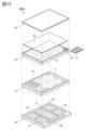
- FIG. 12A and 12B are diagrams for explaining a configuration example of a display device.
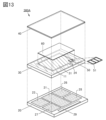
- FIG. 13 is a diagram illustrating a configuration example of a display device.
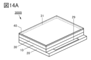
- 14A and 14B are diagrams for explaining a configuration example of a display device.
- FIG. 15 is a diagram illustrating a configuration example of a display device.
- FIG. 16 is a diagram illustrating a configuration example of a display device.
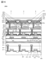
- FIG. 17 is a diagram illustrating a configuration example of a display device.
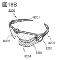
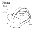
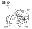
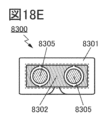
- 18A to 18F are diagrams illustrating examples of electronic devices.
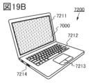
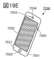
- 19A to 19F are diagrams illustrating examples of electronic devices.
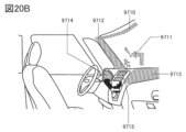
- 20A and 20B are diagrams illustrating an example of an electronic device.
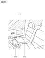
- FIG. 21 is a diagram illustrating an example of an electronic device;
- a semiconductor device is a device that utilizes semiconductor characteristics, and refers to, for example, a circuit including a semiconductor element (eg, a transistor, a diode, a photodiode, or the like), or a device having the same circuit. It also refers to all devices that can function by utilizing semiconductor characteristics. For example, an integrated circuit, a chip with an integrated circuit, or an electronic component containing a chip in a package is an example of a semiconductor device. Further, for example, a storage device, a display device, a light-emitting device, a lighting device, an electronic device, or the like itself may be a semiconductor device and include a semiconductor device.
- a semiconductor element eg, a transistor, a diode, a photodiode, or the like
- connection relationships other than those shown in the drawings or the text are not limited to the predetermined connection relationships, such as the connection relationships shown in the drawings or the text, but are also disclosed in the drawings or the text.
- X and Y are assumed to be objects (eg, devices, elements, circuits, wiring, electrodes, terminals, conductive films, layers, etc.).
- X and Y are electrically connected is an element that enables electrical connection between X and Y (for example, switch, transistor, capacitive element, inductor, resistive element, diode, display devices, light emitting devices, or loads) can be connected between X and Y.
- an element that enables electrical connection between X and Y for example, switch, transistor, capacitive element, inductor, resistive element, diode, display devices, light emitting devices, or loads
- a circuit eg, logic circuit (eg, inverter, NAND circuit, NOR circuit, etc.) that enables functional connection between X and Y).
- a signal conversion circuit for example, a digital-to-analog conversion circuit, an analog-to-digital conversion circuit, or a gamma correction circuit
- a potential level conversion circuit for example, a power supply circuit (for example, a booster circuit, a step-down circuit, etc.), or a signal potential level level shifter circuit, etc.
- voltage source current source
- switching circuit for example, a booster circuit, a step-down circuit, etc.
- amplifier circuit for example, a circuit that can increase the signal amplitude or current amount, operational amplifier, differential amplifier circuit, source follower circuit, buffer circuit, etc.
- signal generator circuit storage circuit, or control circuit
- X and Y are electrically connected, it means that X and Y are electrically connected (that is, another element or another circuit is interposed), and the case where X and Y are directly connected (that is, the case where X and Y are connected without another element or another circuit between them). (if any).
- X and Y the source (or the first terminal, etc.) and the drain (or the second terminal, etc.) of the transistor are electrically connected to each other, and X, the source of the transistor (or the 1 terminal, etc.), the drain of the transistor (or the second terminal, etc.), and are electrically connected in the order of Y.”
- the source (or first terminal, etc.) of the transistor is electrically connected to X
- the drain (or second terminal, etc.) of the transistor is electrically connected to Y
- X the source of the transistor (or the first terminal, etc.), the drain of the transistor (or the second terminal, etc.), and Y are electrically connected in that order.
- X is electrically connected to Y through the source (or first terminal, etc.) and drain (or second terminal, etc.) of the transistor
- X is the source (or first terminal, etc.) of the transistor; terminal, etc.), the drain of the transistor (or the second terminal, etc.), and Y are provided in this connection order.
- the source (or the first terminal, etc.) and the drain (or the second terminal, etc.) of the transistor can be distinguished by defining the order of connection in the circuit configuration.
- the technical scope can be determined.
- these expression methods are examples, and are not limited to these expression methods.
- X and Y are assumed to be objects (for example, devices, elements, circuits, wiring, electrodes, terminals, conductive films, layers, etc.).
- circuit diagram shows independent components electrically connected to each other, if one component has the functions of multiple components.
- one component has the functions of multiple components
- the term "electrically connected" in this specification and the like includes such a case where one conductive film functions as a plurality of constituent elements.
- a “resistive element” can be, for example, a circuit element or wiring having a resistance value higher than 0 ⁇ . Therefore, in this specification and the like, the “resistive element” includes, for example, a wiring having a resistance value, a transistor, a diode, or a coil through which current flows between the source and the drain. Therefore, the term “resistive element” can be replaced with terms such as “resistance”, "load”, or "region having a resistance value”. Conversely, the terms “resistor”, “load”, or “region having a resistance value” can be interchanged with terms such as, for example, “resistive element”.
- the resistance value can be, for example, preferably 1 m ⁇ or more and 10 ⁇ or less, more preferably 5 m ⁇ or more and 5 ⁇ or less, still more preferably 10 m ⁇ or more and 1 ⁇ or less. Also, for example, it may be 1 ⁇ or more and 1 ⁇ 10 9 ⁇ or less.
- the resistance value of the resistance element may be determined depending on the length of the wiring.
- the resistance element may use a conductor having a resistivity different from that of the conductor used as the wiring.
- the resistance value of the resistance element may be determined by doping impurities into the semiconductor.
- the term “capacitance element” refers to, for example, a circuit element having a capacitance value higher than 0 F, a wiring region having a capacitance value higher than 0 F, a parasitic capacitance, or It can be a gate capacitance of a transistor or the like. Therefore, in this specification and the like, the term “capacitor” is not limited to a circuit element including a pair of electrodes and a dielectric material included between the electrodes.
- the “capacitive element” includes, for example, parasitic capacitance generated between wirings, or gate capacitance generated between one of the source or drain of a transistor and the gate.
- capacitor element terms such as “capacitance element”, “parasitic capacitance”, or “gate capacitance” can be replaced with terms such as “capacitance”.
- capacitor shall be interchangeable with terms such as, for example, “capacitance element”, “parasitic capacitance”, or “gate capacitance”.
- a pair of electrodes in the “capacitance” can be replaced with, for example, a "pair of conductors", a “pair of conductive regions", or a “pair of regions”.
- the value of the capacitance can be, for example, 0.05 fF or more and 10 pF or less. Also, for example, it may be 1 pF or more and 10 ⁇ F or less.
- a transistor has three terminals called a gate, a source, and a drain.
- the gate is the control terminal that controls the amount of current that flows between the source and drain.
- the two terminals functioning as source or drain are the input and output terminals of the transistor.
- One of the two input/output terminals functions as a source and the other as a drain, depending on the conductivity type (n-channel type or p-channel type) of the transistor and the level of potentials applied to the three terminals of the transistor. Therefore, in this specification and the like, the terms “source” and “drain” can be used interchangeably.
- a transistor may have a back gate in addition to the above three terminals depending on its structure.
- one of the gate and back gate of the transistor may be referred to as a first gate
- the other of the gate and back gate of the transistor may be referred to as a second gate.
- the terms "gate” and “backgate” may be used interchangeably for the same transistor.
- each gate may be referred to as a first gate, a second gate, a third gate, or the like in this specification and the like.
- node may be used in accordance with, for example, the circuit configuration or device structure, for example, “terminal”, “wiring”, “electrode”, “conductive layer”, “conductor”, Alternatively, it can be rephrased as an “impurity region” or the like. Also, for example, a “terminal” or “wiring” can be rephrased as a “node”.
- Voltage is a potential difference from a reference potential.
- the reference potential is ground potential
- “voltage” can be rephrased as “potential”. Note that the ground potential does not necessarily mean 0V. Also, potentials are relative. That is, when the reference potential changes, for example, the potential applied to the wiring, the potential applied to the circuit, or the potential output from the circuit also changes.
- high-level potential also referred to as “high-level potential”, “H potential”, or “H”
- low-level potential also referred to as “low-level potential”, “L potential”, or The term “L”
- high-level potential also referred to as “high-level potential”, “H potential”, or “H”
- low-level potential also referred to as “low-level potential”, “L potential”, or The term “L”
- the term “current” refers to a charge transfer phenomenon (electrical conduction).
- electrical conduction of positively charged bodies occurs can be rephrased as “electrical conduction of negatively charged bodies occurs in the opposite direction”. Therefore, in this specification and the like, unless otherwise specified, the term “electric current” refers to a charge transfer phenomenon (electrical conduction) associated with the movement of carriers. Examples of carriers here include electrons, holes, anions, cations, complex ions, and the like. Note that the carrier differs depending on the current-flowing system (for example, semiconductor, metal, electrolyte, or in vacuum).
- the “direction of current” in a wiring or the like is defined as the direction in which positive carriers move, and is described as a positive amount of current.
- the direction in which negative carriers move is opposite to the direction of the current, and is represented by the amount of negative current. Therefore, in this specification and the like, when there is no indication about the positive or negative of the current (or the direction of the current), for example, the description such as “current flows from element A to element B” is replaced with “current flows from element B to element A.” It can be rephrased as "flowing”. Also, for example, a description such as "a current is input to the element A” can be replaced with, for example, "a current is output from the element A”.
- the ordinal numbers “first”, “second”, and “third” are added to avoid confusion of constituent elements. Therefore, the number of components is not limited. Also, the order of the components is not limited. For example, a component referred to as “first” in one embodiment such as this specification is a component referred to as “second” in other embodiments or claims. It is also possible. Also, for example, a component referred to as “first” in one embodiment of this specification may be omitted in another embodiment or the scope of claims.
- electrode B on insulating layer A does not necessarily mean that electrode B is formed on insulating layer A in direct contact, and another component is provided between insulating layer A and electrode B. Do not exclude what is included.
- Electrode B overlapping insulating layer A is not limited to the state in which electrode B is formed on insulating layer A.
- the expression “electrode B overlapping the insulating layer A” means, for example, a state in which the electrode B is formed under the insulating layer A, or a state in which the electrode B is formed on the right side (or left side) of the insulating layer A. , etc. are not excluded.
- the term “adjacent” or “adjacent” does not limit that components are in direct contact with each other.
- the expression “electrode B adjacent to insulating layer A” does not necessarily mean that insulating layer A and electrode B are formed in direct contact, and other components are provided between insulating layer A and electrode B. Do not exclude what is included.
- terms such as “film” and “layer” may be interchanged depending on the situation.
- the term “conductive layer” may be changed to the term “conductive film.”
- the term “insulating film” may be changed to the term “insulating layer.”
- terms such as “film” or “layer” may not be used and may be replaced with other terms depending on the situation.
- the term “conductive layer” or “conductive film” may be changed to the term “conductor.”
- the term “conductor” may be changed to the term “conductive layer” or “conductive film”.
- the term “insulating layer” or “insulating film” may be changed to the term “insulator.”
- the term “insulator” may be changed to the term "insulating layer” or “insulating film”.
- Electrode may be used as part of a “wiring” and vice versa.
- the term “electrode” or “wiring” includes, for example, the case where a plurality of “electrodes” or “wiring” are integrally formed.
- terminal may be used as part of “wiring” or “electrode”, and vice versa.
- terminal includes, for example, a case in which a plurality of "electrodes", “wirings", or “terminals” are integrally formed.
- an "electrode” can be part of a “wiring” or a “terminal”.
- a “terminal” can be part of a “wiring” or an “electrode”.
- terms such as “electrode”, “wiring”, or “terminal” may be replaced with terms such as “region”.
- terms such as “wiring”, “signal line”, and “power line” may be interchanged depending on the situation.
- the term “wiring” may be changed to the term “signal line.”
- the term “wiring” may be changed to a term such as “power supply line”.
- terms such as “signal line” or “power line” may be changed to the term “wiring”.
- a term such as “power line” may be changed to a term such as “signal line”.
- a term such as “signal line” may be changed to a term such as “power line”.
- the term “potential” applied to the wiring may be changed to, for example, the term “signal” depending on the situation. And vice versa, for example, terms such as “signal” may be changed to the term “potential”.
- a “switch” has a plurality of terminals and has a function of switching (selecting) conduction or non-conduction between the terminals.
- a switch is said to be “conducting” or “on” if it has two terminals and there is electrical continuity between the two terminals.
- the switch is said to be “non-conducting” or “off”. Note that switching to one of the conducting state and the non-conducting state or maintaining one of the conducting state and the non-conducting state of the switch is sometimes referred to as "controlling the conducting state.”
- a switch has a function of controlling whether or not to allow current to flow.
- a switch is one that has a function of selecting and switching a path through which current flows.
- the switch for example, an electrical switch or a mechanical switch can be used.
- the switch is not limited to a specific one as long as it can control current.
- switch As a type of switch, there is a switch that is normally in a non-conducting state and becomes a conducting state by controlling the conducting state, and such a switch is sometimes called an "A contact". As a type of switch, there is a switch that is normally in a conducting state and becomes non-conducting by controlling the conducting state, and such a switch is sometimes called a "B contact”.
- switches include transistors (eg, bipolar transistors, MOS transistors, etc.), diodes (eg, PN diodes, PIN diodes, Schottky diodes, MIM (Metal Insulator Metal) diodes, MIS (Metal Insulator Semiconductor) diodes, , or diode-connected transistors), or a logic circuit combining these.
- transistors eg, bipolar transistors, MOS transistors, etc.
- diodes eg, PN diodes, PIN diodes, Schottky diodes, MIM (Metal Insulator Metal) diodes, MIS (Metal Insulator Semiconductor) diodes, , or diode-connected transistors
- MIM Metal Insulator Metal
- MIS Metal Insulator Semiconductor
- a “non-conducting state” or an “off state” of a transistor means a state in which a source electrode and a drain electrode of the transistor can be considered to be electrically cut off. Note that the polarity (conductivity type) of the transistor is not particularly limited when the transistor is operated as a simple switch.
- a mechanical switch is a switch using MEMS (Micro Electro Mechanical Systems) technology.
- the switch has an electrode that can be moved mechanically, and selects a conducting state or a non-conducting state by moving the electrode.
- parallel means a state in which two straight lines are arranged at an angle of ⁇ 10° or more and 10° or less. Therefore, the case of ⁇ 5° or more and 5° or less is also included.
- substantially parallel or “substantially parallel” refers to a state in which two straight lines are arranged at an angle of -30° or more and 30° or less.
- Perfect means that two straight lines are arranged at an angle of 80° or more and 100° or less. Therefore, the case of 85° or more and 95° or less is also included.
- count values and metric values or regarding substances, methods, events, etc. that can be converted to count values or metric values, for example, “same”, “same”, “equal”, or References such as “uniform” (including synonyms thereof) are intended to include a margin of error of plus or minus 20%, unless explicitly stated.
- an impurity of a semiconductor means, for example, other than the main component that constitutes a semiconductor layer.
- impurities for example, the defect level density of the semiconductor may be increased, the carrier mobility may be decreased, or the crystallinity may be decreased.
- impurities that change the characteristics of the semiconductor include, for example, Group 1 elements, Group 2 elements, Group 13 elements, Group 14 elements, Group 15 elements, or oxides.
- transition metals other than the main components of semiconductors.
- the impurities that change the characteristics of the semiconductor include, for example, group 1 elements excluding oxygen and hydrogen, group 2 elements, group 13 elements, or group 15 elements. be.
- a metal oxide is a metal oxide in a broad sense.
- Metal oxides are classified into, for example, oxide insulators, oxide conductors (including transparent oxide conductors), oxide semiconductors (also referred to as oxide semiconductors or simply OSs), and the like.
- oxide semiconductors also referred to as oxide semiconductors or simply OSs
- the metal oxide is sometimes called an oxide semiconductor. That is, when a metal oxide is used as a channel forming region of a transistor having at least one of amplifying action, rectifying action, and switching action, the metal oxide is a metal oxide semiconductor. semiconductor).
- the description of the “OS transistor” can be paraphrased as a transistor including a metal oxide or an oxide semiconductor.
- nitrogen-containing metal oxides may also be collectively referred to as metal oxides.
- Metal oxides containing nitrogen may also be referred to as metal oxynitrides.
- arrows indicating the X direction, the Y direction, and the Z direction may be attached in the drawings and the like according to this specification.
- the “X direction” is the direction along the X axis, and the forward direction and the reverse direction may not be distinguished unless explicitly stated.
- the X direction, the Y direction, and the Z direction are directions that cross each other. More specifically, the X-direction, Y-direction, and Z-direction are directions orthogonal to each other.
- first direction or “first direction”
- second direction or a “second direction”
- third direction or “third direction”.
- the code is, for example, "A”, “b”, “_1", “[n]", Alternatively, an identification code such as "[m, n]" may be added.
- a semiconductor device according to one embodiment of the present invention will be described.
- a semiconductor device can be used, for example, in a driver circuit for driving a pixel circuit included in a display device.
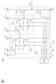
- FIG. 1 shows a circuit configuration example of the semiconductor device 100A.
- the semiconductor device 100A includes a level shifter section 101A and a logic circuit section 102A.
- the level shifter section 101A has a plurality of input terminals and at least one output terminal.
- the logic circuit section 102A has a plurality of output terminals. Each of the plurality of input terminals provided in the level shifter section 101A is electrically connected to each of the plurality of output terminals provided in the logic circuit section 102A.
- each of four input terminals (input terminal portion 101Ain) included in the level shifter portion 101A is connected to a logic circuit via a wiring IN, a wiring RST, a wiring SW1, and a wiring SW2. It is electrically connected to each of the four output terminals of the section 102A. Further, an output terminal included in the level shifter section 101A is electrically connected to the wiring OUT.
- the logic circuit portion 102A has a function of outputting a signal necessary for the operation of the level shifter portion 101A to each of the wiring IN, the wiring RST, the wiring SW1, and the wiring SW2.
- the level shifter portion 101A has a function of using signals input from each of the wiring IN, the wiring RST, the wiring SW1, and the wiring SW2, and outputting a signal boosted to a higher potential than the input signal to the wiring OUT.
- the semiconductor device 100A according to one embodiment of the present invention has a function of outputting a signal having a larger amplitude than the signal output from the logic circuit portion 102A through the level shifter portion 101A.
- the level shifter section 101A includes a signal boosting section 104Aa and a signal output section 103A.
- the signal boosting section 104Aa includes a boosting stage 105A_1 and a boosting stage 105A_2.
- Boosting stage 105A_1 includes transistor M13_1, transistor M14_1, transistor M15_1, and capacitor C11_1.
- Boosting stage 105A_2 includes transistor M13_2, transistor M14_2, transistor M15_2, and capacitor C11_2.
- the signal output section 103A includes a transistor M11 and a transistor M12.
- the gate of the transistor M13_1 is electrically connected to the wiring P13_1, one of its source and drain is electrically connected to the gate of the transistor M14_1, and the other is electrically connected to the wiring P10.
- one of the source and the drain of the transistor M14_1 is electrically connected to one of the source and the drain of the transistor M15_1, and the other is electrically connected to the wiring P14_1.
- the gate of the transistor M15_1 is electrically connected to the wiring RST, and the other of the source and the drain is electrically connected to the wiring P12.
- One terminal of the capacitor C11_1 is electrically connected to the gate of the transistor M14_1, and the other terminal is electrically connected to the wiring SW1.
- the gate of the transistor M13_2 is electrically connected to the wiring P13_2, one of its source and drain is electrically connected to the gate of the transistor M14_2, and the other is electrically connected to one of the source and drain of the transistor M14_1.
- one of the source and the drain of the transistor M14_2 is electrically connected to one of the source and the drain of the transistor M15_2, and the other is electrically connected to the wiring P14_2.
- the gate of the transistor M15_2 is electrically connected to the wiring RST, and the other of the source and the drain is electrically connected to the wiring P12.
- One terminal of the capacitor C11_2 is electrically connected to the gate of the transistor M14_2, and the other terminal is electrically connected to the wiring SW2.
- a gate of the transistor M11 is electrically connected to one of the source and the drain of the transistor M14_2, one of the source and the drain is electrically connected to the wiring OUT, and the other is electrically connected to the wiring P11.
- the gate of the transistor M12 is electrically connected to the wiring IN, one of its source and drain is electrically connected to the wiring OUT, and the other is electrically connected to the wiring P12.
- a region where one of the source and drain of the transistor M13_1, the gate of the transistor M14_1, and one terminal of the capacitor C11_1 are electrically connected to each other is also referred to as a node N11_1.
- a region where one of the source and drain of the transistor M14_1, one of the source and drain of the transistor M15_1, and the other of the source and drain of the transistor M13_2 are electrically connected to each other is also referred to as a node N12_1.
- a region where one of the source and drain of the transistor M13_2, the gate of the transistor M14_2, and one terminal of the capacitor C11_2 are electrically connected to each other is also referred to as a node N11_2.
- a region where one of the source and drain of the transistor M14_2, one of the source and drain of the transistor M15_2, and the gate of the transistor M11 are electrically connected to each other is also referred to as a node N12_2.
- the capacitor C11_1 has a function of changing the potential of the node N11_1 according to the signal supplied to the wiring SW1.
- the capacitor C11_2 has a function of changing the potential of the node N11_2 according to the signal supplied to the wiring SW2.
- the level shifter portion 101A included in the semiconductor device 100A has a function of changing the potential by capacitive coupling in the signal boosting portion. Therefore, in this specification and the like, a circuit configuration such as the level shifter section 101A may be referred to as a "capacitive coupling type level shifter”.
- a transistor including various semiconductors can be used for the semiconductor device 100A according to one embodiment of the present invention.
- a transistor including a single crystal semiconductor, a polycrystalline semiconductor, a microcrystalline semiconductor, or an amorphous semiconductor for a channel formation region can be used.
- the main component is not limited to a single semiconductor (for example, silicon (Si) or germanium (Ge)) composed of a single element.
- Gallium (GaAs)), an oxide semiconductor, or the like can be used.
- transistors with various structures can be used for the semiconductor device 100A according to one embodiment of the present invention.
- planar type FIN type (fin type), TRI-GATE type (tri-gate type), top gate type, bottom gate type, or dual gate type (a structure in which gates are arranged above and below a channel).
- a transistor with any structure can be used.
- a transistor according to one embodiment of the present invention a MOS transistor, a junction transistor, a bipolar transistor, or the like can be used, for example.
- the semiconductor device 100A may be configured with a plurality of types of transistors using different semiconductor materials.
- the logic circuit section 102A a Si transistor (a transistor containing silicon in a semiconductor layer where a channel is formed), and configure the level shifter section 101A with an OS transistor (a transistor containing an oxide semiconductor in a semiconductor layer where a channel is formed). It is preferable to configure with
- Si transistors operate faster than OS transistors.
- a CMOS circuit for example, a circuit that operates complementarily, a CMOS logic gate, a CMOS logic circuit, etc.
- the operation speed of the logic circuit portion 102A can be increased, and power consumption in a steady state can be reduced.
- An OS transistor has a higher dielectric breakdown voltage between a source and a drain than a Si transistor with the same channel size. Therefore, in the semiconductor device 100A according to one embodiment of the present invention, an OS transistor is used as a transistor included in the level shifter portion 101A, so that a voltage higher than the dielectric strength voltage of the Si transistor is applied between the source and the drain of the transistor. can be run by Moreover, even when a high voltage is applied, the operation is stable, and a highly reliable semiconductor device can be realized.
- the upper limit of the amplitude of the signal output from the logic circuit section 102A composed of Si transistors is determined by the withstand voltage of the Si transistors. Therefore, by forming the level shifter portion 101A with an OS transistor having a higher withstand voltage than a Si transistor, the semiconductor device 100A according to one embodiment of the present invention can transmit a signal having a larger amplitude than the signal output from the logic circuit portion 102A. It can be output via the level shifter section 101A.
- Si transistors with increased dielectric strength also referred to as high-voltage Si transistors
- the high-voltage Si transistors are Si transistors that make up the logic circuit section 102A. If it is manufactured separately from the transistor, the manufacturing cost for manufacturing the high-voltage Si transistor increases.
- the semiconductor device 100A according to one aspect of the present invention can configure the level shifter section 101A without employing a high-voltage Si transistor. Therefore, manufacturing costs can be reduced.
- an oxide semiconductor in which a channel of an OS transistor is formed has a bandgap of 2 eV or more, and thus has significantly low off-state current.
- the off-current value of the OS transistor per 1 ⁇ m channel width at room temperature is 1 aA (1 ⁇ 10 ⁇ 18 A) or less, 1 zA (1 ⁇ 10 ⁇ 21 A) or less, or 1 yA (1 ⁇ 10 ⁇ 24 A) or less.
- the off current value of the Si transistor per 1 ⁇ m channel width at room temperature is 1 fA (1 ⁇ 10 ⁇ 15 A) or more and 1 pA (1 ⁇ 10 ⁇ 12 A) or less. Therefore, it can be said that the off-state current of the OS transistor is about ten digits lower than the off-state current of the Si transistor.
- the boosted potential of each node can be held for a long time.
- the off current of the OS transistor hardly increases even in a high temperature environment. Specifically, the off-state current hardly increases even under an environmental temperature of room temperature or higher and 200° C. or lower. Also, the on-current is less likely to decrease even in a high-temperature environment.
- a semiconductor device including an OS transistor can operate stably and have high reliability even in a high-temperature environment.
- a semiconductor layer of the OS transistor preferably contains at least one of indium and zinc.
- the semiconductor layer of the OS transistor includes, for example, indium and M (M is gallium, aluminum, yttrium, tin, silicon, boron, copper, vanadium, beryllium, titanium, iron, nickel, germanium, zirconium, molybdenum, lanthanum, , cerium, neodymium, hafnium, tantalum, tungsten, magnesium, and cobalt) and zinc.
- M is preferably one or more selected from gallium, aluminum, yttrium and tin.
- an oxide containing indium (In), gallium (Ga), and zinc (Zn) is preferably used for the semiconductor layer.
- an oxide containing indium (In), aluminum (Al), and zinc (Zn) also referred to as “IAZO”
- IAZO oxide containing indium (In), aluminum (Al), gallium (Ga), and zinc (Zn)
- IAGZO oxide containing indium (In), aluminum (Al), gallium (Ga), and zinc (Zn)
- the In atomic ratio in the In-M-Zn oxide is preferably equal to or higher than the M atomic ratio.
- the atomic ratio of In in the In--M--Zn oxide may be smaller than the atomic ratio of M in some cases.
- the composition in the neighborhood includes the range of plus or minus 30% of the desired atomic number ratio.
- the content ratio of each element is 1 or more and 3 or less for Ga when In is 4, The case where Zn is 2 or more and 4 or less is included.
- the content ratio of each element is such that when In is 5, Ga is greater than 0.1 and 2 or less, including the case where Zn is 5 or more and 7 or less.
- the content ratio of each element is such that when In is 1, Ga is greater than 0.1 and 2 or less, including the case where Zn is greater than 0.1 and 2 or less.
- the transistors may be provided in different layers for each type of transistor.
- the Si transistors forming the logic circuit section 102A and the OS transistors forming the level shifter section 101A may be provided in different layers.
- a layer including a Si transistor eg, a layer provided with the logic circuit portion 102A
- a layer including an OS transistor eg, a layer provided with the level shifter portion 101A
- the area occupied by the semiconductor device 100A is reduced. Therefore, miniaturization of the semiconductor device 100A can be realized.
- the semiconductor device 100A can be used, for example, as a driver circuit for driving a pixel circuit included in a display device.
- An OS transistor may be used as a transistor included in the pixel circuit.
- the pixel circuit may be provided in the same layer as the layer in which the level shifter portion 101A is provided, or may be provided in a different layer. When they are provided in different layers, the layer provided with the pixel circuit and the layer provided with the level shifter portion 101A may be provided so as to overlap each other. A detailed description of a display device using a semiconductor device according to one embodiment of the present invention will be given later.
- All or part of the transistors forming the semiconductor device 100A may be transistors having back gates.
- the back gate By providing the back gate, an electric field generated outside the transistor is less likely to act on the channel formation region, so that the operation of the semiconductor device can be stabilized and the reliability of the semiconductor device can be improved. Further, by applying the same potential to the back gate as that of the gate, the on-resistance of the transistor can be reduced.
- the threshold voltage of the transistor can be changed by controlling the potential of the back gate independently of the potential of the gate.
- FIG. 2 shows a circuit configuration example in which the level shifter section 101A of the semiconductor device 100A is composed of transistors having back gates.
- FIG. 2 shows an example of electrically connecting the gate and the back gate of each of the transistor M11, the transistor M12, the transistor M13_1, the transistor M14_1, the transistor M15_1, the transistor M13_2, the transistor M14_2, and the transistor M15_2.
- an arbitrary potential may be supplied to the back gate without electrically connecting the gate and the back gate.
- the potential supplied to the back gate is not limited to the fixed potential.
- the potentials supplied to the back gates of the transistors included in the semiconductor device may be different or the same for each transistor.
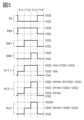
- FIG. 3 is a timing chart for explaining an operation example of the semiconductor device 100A.
- the logic circuit section 102A included in the semiconductor device 100A operates by supplying the potential VSS and the potential VDD, for example. Therefore, the potential of the signal output from the logic circuit portion 102A (the signal supplied to each of the wiring IN, the wiring RST, the wiring SW1, and the wiring SW2) is the potential VSS or the potential VDD. Note that in this embodiment and the like, when a Si transistor is used in the logic circuit portion 102A, the potential difference between the potential VDD and the potential VSS (potential VDD ⁇ potential VSS) is preferably higher than the threshold voltage of the Si transistor. , is preferably lower than the withstand voltage of the Si transistor.
- the level shifter portion 101A supplies, for example, the potential VDDH to the wiring P11, the potential VSS to the wiring P12, and the potential V10 and the potential V10 to the wiring P10, the wiring P13_1, the wiring P14_1, the wiring P13_2, and the wiring P14_2, respectively.
- V13_1, the potential V14_1, the potential V13_2, and the potential V14_2 are supplied to the wiring OUT based on the signals supplied from the logic circuit portion 102A to the wiring IN, the wiring RST, the wiring SW1, and the wiring SW2. It has a function of outputting potential VDDH or potential VSS.
- each of the potential VDDH, the potential V10, the potential V13_1, the potential V14_1, the potential V13_2, and the potential V14_2 is higher than the potential VDD. good too.
- the potential VSS is set to 0 V and the potential VDD is set to 3 V, for example.
- the potential VDDH is set to 6V.
- the potential V10, the potential V13_1, the potential V14_1, the potential V13_2, and the potential V14_2 are assumed to be 3 V, 4 V, 6 V, 6 V, and 7 V, respectively.
- the threshold voltage Vth of the transistor (for example, the OS transistor) forming the level shifter section 101A is assumed to be 1V.
- a period T11 to a period T13 are periods in which an operation of outputting a high potential (potential VDDH) to the wiring OUT is performed.
- the potential VSS (0 V) is supplied to the wiring IN. Further, the potential VSS (0 V) is supplied to each of the wiring RST, the wiring SW1, and the wiring SW2. Then, the transistor M12 is turned off. Further, the transistor M15_1 and the transistor M15_2 are off.
- the potentials of the node N11_1, the node N12_1, the node N11_2, the node N12_2, and the wiring OUT are 3 V, 2 V, 2 V, 1 V, and 0 V, respectively.
- the potential VDD (3 V) is supplied to the wiring SW1.
- the potential of the node N11_1 increases by the potential difference (3 V) of "potential VDD-potential VSS".
- the potential of the node N11_1 is maintained by appropriately setting the potential V13_1 so that the transistor M13_1 is turned off.
- the potentials of the nodes N12_1, N11_2, N12_2, and the wiring OUT increase.
- the potentials of the node N11_1, the node N12_1, the node N11_2, the node N12_2, and the wiring OUT are 6 V, 5 V, 5 V, 4 V, and 3 V, respectively.
- the potential VDD (3 V) is supplied to the wiring SW2.
- the potential of the node N11_2 increases by the potential difference (3 V) of "potential VDD-potential VSS".
- the potential of the node N11_2 is maintained by appropriately setting the potential V13_2 so that the transistor M13_2 is turned off.
- the potentials of the node N12_2 and the wiring OUT also increase.
- the potentials of the node N11_1, the node N12_1, the node N11_2, the node N12_2, and the wiring OUT are 6V, 5V, 8V, 7V, and 6V, respectively.
- a period T14 and a period T15 are periods in which an operation of outputting a low potential (potential VSS) to the wiring OUT is performed.
- the potential VDD (3 V) is supplied to each of the wirings IN and RST, and the potential VSS (0 V) is supplied to each of the wirings SW1 and SW2. Then, the transistor M12, the transistor M15_1, and the transistor M15_2 are turned on. Therefore, the potential VSS (0 V) is supplied to the node N12_1, the node N11_2, the node N12_2, and the wiring OUT. Then, the transistor M14_2 and the transistor M11 are turned off.
- the potential of the node N11_1 is the potential V10, that is, 3V. Therefore, the transistor M14_1 is turned on, and current flows from the wiring P14_1 to the wiring P12 through the transistors M14_1 and M15_1. Therefore, the period T14 is preferably short, and the operation in the next period T15 is preferably performed when the transistor M14_2 and the transistor M11 are turned off.
- the potential VSS (0 V) is supplied to the wiring RST.
- a potential VDD (3 V) is supplied to the wiring IN.
- the transistor M15_1 and the transistor M15_2 are turned off. Also, the transistor M12 is on.
- the potentials of the node N11_1, the node N12_1, the node N11_2, the node N12_2, and the wiring OUT are 3 V, 2 V, 2 V, 1 V, and 0 V, respectively.
- the semiconductor device 100A can output a potential boosted from the potential VDD (3 V) to the potential VDDH (6 V) by performing operations in the periods T11 to T13. By performing the operations in the periods T14 and T15, the potential VSS (0 V) can be output.
- a Si transistor can be used as a transistor included in the logic circuit portion 102A, and an OS transistor can be used as a transistor included in the level shifter portion 101A.
- An OS transistor has a higher withstand voltage than a Si transistor.
- the semiconductor device 100A according to one embodiment of the present invention is not limited to the circuit configuration shown in FIG. FIG. 4 shows another circuit configuration example of the semiconductor device 100A. Note that, in order to reduce the repetition of the description, mainly the differences of the semiconductor device 100A shown in FIG. 4 from the semiconductor device 100A shown in FIG. 1 will be explained. Further, the description of the configuration example described above can be appropriately referred to.
- the semiconductor device 100A shown in FIG. 4 includes a signal booster 104Ab instead of the signal booster 104Aa included in the semiconductor device 100A shown in FIG.
- the signal boosting section 104Ab includes a boosting stage 105A_1 and a capacitor C12.
- the signal boosting section 104Aa has a configuration example including two boosting stages (boosting stage 105A_1 and boosting stage 105A_2). A configuration including a boosting stage may also be used.
- the potential can be raised by capacitive coupling by the potential difference (3 V) of "potential VDD-potential VSS" for each step-up stage. Therefore, the number of boosting stages should be appropriately selected according to the potential to be output.
- the signal boosting section 104Ab includes one boosting stage (105A_1).
- the other of the source and the drain of the transistor M13_1 is electrically connected to the logic circuit portion 102A through the wiring INB.
- a gate of the transistor M15_1 is electrically connected to the wiring IN.
- the gate of the transistor M11 is electrically connected to one of the source and the drain of the transistor M14_1.
- One terminal of the capacitor C12 is electrically connected to the gate of the transistor M11, and the other terminal is electrically connected to the wiring SW2. That is, the wire SW2 and the node N12_1 are capacitively coupled via the capacitor C12. Therefore, the capacitor C12 has a function of changing the potential of the node N12_1 according to the signal supplied to the wiring SW2.
- FIG. 5 is a timing chart for explaining an operation example of the semiconductor device 100A shown in FIG. In order to reduce the repetition of the description, mainly the differences from the operation example described above will be described. Further, the description of the operation example described above can be appropriately referred to.
- the wiring INB is supplied with a logical negation signal (also referred to as an inverted signal) of the signal supplied to the wiring IN. That is, when the potential VDD (3 V) is supplied to the wiring IN, the potential VSS (0 V) is supplied to the wiring INB. Alternatively, when the potential VSS (0 V) is supplied to the wiring IN, the potential VDD (3 V) is supplied to the wiring INB. Further, as an example, the potential V13_1 and the potential V14_1 are assumed to be 3 V and 6 V, respectively.
- a period T11 to a period T13 are periods in which an operation of outputting a high potential (potential VDDH) to the wiring OUT is performed.
- a potential VDD (3 V) is supplied to the wiring INB, and the above operation example can be referred to as appropriate.
- the potentials of the node N11_1, the node N12_1, and the wiring OUT are 2 V, 1 V, and 0 V, respectively. Further, in the period T12, the potentials of the node N11_1, the node N12_1, and the wiring OUT are 5 V, 4 V, and 3 V, respectively. Further, in the period T13, the potentials of the node N11_1, the node N12_1, and the wiring OUT are 5 V, 7 V, and 6 V, respectively.
- a period T14 is a period in which an operation of outputting a low potential (potential VSS) to the wiring OUT is performed.
- a potential VDD (3 V) is supplied to the wiring IN, and a potential VSS (0 V) is supplied to each of the wiring INB, the wiring SW1, and the wiring SW2. Then, the transistor M12, the transistor M13_1, and the transistor M15_1 are turned on. Therefore, the potential VSS (0 V) is supplied to the node N11_1, the node N12_1, and the wiring OUT. Then, the transistor M14_1 and the transistor M11 are turned off.
- the potentials of the node N11_1, the node N12_1, and the wiring OUT are 0 V, 0 V, and 0 V, respectively.
- the semiconductor device 100A illustrated in FIG. 4 can output a potential boosted from the potential VDD (3 V) to the potential VDDH (6 V) by performing the operations in the periods T11 to T13 illustrated in FIG. , the potential VSS (0 V) can be output by performing the operation in the period T14.
- a semiconductor device 100B according to one embodiment of the present invention will be described.
- a semiconductor device 100B is a modification of the semiconductor device 100A. Therefore, in order to reduce the repetition of the description, mainly the points of difference between the semiconductor device 100B and the semiconductor device 100A will be described. Further, the description of the semiconductor device 100A described above can be appropriately referred to.
- FIG. 6 shows a circuit configuration example of the semiconductor device 100B.
- the semiconductor device 100B includes a level shifter section 101B and a logic circuit section 102B.
- the level shifter section 101B has a plurality of input terminals and at least one output terminal.
- the logic circuit section 102B has a plurality of output terminals. Each of the plurality of input terminals included in the level shifter section 101B is electrically connected to each of the plurality of output terminals included in the logic circuit section 102B.
- each of the four input terminals (input terminal portion 101Bin) included in the level shifter portion 101B is connected to the logic circuit via the wiring IN, the wiring RST, the wiring CK, and the wiring CKB. It is electrically connected to each of the four output terminals of section 102B. An output terminal of the level shifter portion 101B is electrically connected to the wiring OUT.
- the logic circuit portion 102B has a function of outputting signals necessary for the operation of the level shifter portion 101B to the wiring IN, the wiring RST, the wiring CK, and the wiring CKB.
- the level shifter portion 101B has a function of using signals input from each of the wiring IN, the wiring RST, the wiring CK, and the wiring CKB to boost the potential of the input signal to be higher than that of the input signal, and output the signal to the wiring OUT.
- the semiconductor device 100B according to one embodiment of the present invention has a function of outputting a signal having a larger amplitude than the signal output from the logic circuit portion 102B through the level shifter portion 101B.
- the level shifter section 101B includes a signal boosting section 104B and a signal output section 103B.
- the signal boosting section 104B includes a boosting stage 105B_1, a boosting stage 105B_2, a boosting stage 105B_3, a transistor M24, and a transistor M25.
- Boosting stage 105B_1 includes transistor M23_1 and capacitor C21_1.
- Boosting stage 105B_2 includes transistor M23_2 and capacitor C21_2.
- Boosting stage 105B_3 includes transistor M23_3 and capacitor C21_3.
- the signal output section 103B includes a transistor M21 and a transistor M22.
- the transistor M23_1 is diode-connected.
- the anode side of the diode-connected transistor M23_1 is electrically connected to the wiring P20, and the cathode side is electrically connected to one terminal of the capacitor C21_1.
- the other terminal of the capacitor C21_1 is electrically connected to the wiring CK.
- the transistor M23_2 is diode-connected.
- the anode side of the diode-connected transistor M23_2 is electrically connected to the cathode side of the diode-connected transistor M23_1, and the cathode side is electrically connected to one terminal of the capacitor C21_2.
- the other terminal of the capacitor C21_2 is electrically connected to the wiring CKB.
- the transistor M23_3 is diode-connected.
- the anode side of the diode-connected transistor M23_3 is electrically connected to the cathode side of the diode-connected transistor M23_2, and the cathode side is electrically connected to one terminal of the capacitor C21_3.
- the other terminal of the capacitor C21_3 is electrically connected to the wiring CK.
- Transistor M24 is diode-connected.
- the anode side of the diode-connected transistor M24 is electrically connected to the cathode side of the diode-connected transistor M23_3, and the cathode side is electrically connected to either the source or the drain of the transistor M25.
- a gate of the transistor M25 is electrically connected to the wiring RST, and the other of the source and the drain is electrically connected to the wiring P22.
- the gate of the transistor M21 is electrically connected to the cathode side of the diode-connected transistor M24, one of the source and the drain is electrically connected to the wiring OUT, and the other is electrically connected to the wiring P21.
- the gate of the transistor M22 is electrically connected to the wiring IN, one of its source and drain is electrically connected to the wiring OUT, and the other is electrically connected to the wiring P22.
- a region where the cathode side of the diode-connected transistor M23_1, one terminal of the capacitor C21_1, and the anode side of the diode-connected transistor M23_2 are electrically connected to each other is also referred to as a node N21_1.
- a region where the cathode side of the diode-connected transistor M23_2, one terminal of the capacitor C21_2, and the anode side of the diode-connected transistor M23_3 are electrically connected to each other is also referred to as a node N21_2.
- a region where the cathode side of the diode-connected transistor M23_3, one terminal of the capacitor C21_3, and the anode side of the diode-connected transistor M24 are electrically connected to each other is also referred to as a node N21_3.
- a region where the diode-connected cathode side of the transistor M24, one of the source or drain of the transistor M25, and the gate of the transistor M21 are electrically connected to each other is also referred to as a node N22.
- the signal boosting portion 104B forms a charge pump and has a function of gradually increasing the potential of the node N22 by supplying clock signals to the wirings CK and CKB.
- the level shifter portion 101B included in the semiconductor device 100B has a function of raising the potential by a charge pump in the signal boosting portion. Therefore, in this specification and the like, a circuit configuration such as the level shifter section 101B may be referred to as a "charge-pump type level shifter”.
- a transistor including various semiconductors can be used for the semiconductor device 100B according to one embodiment of the present invention, similarly to the semiconductor device 100A.
- the semiconductor device 100B can output a signal having a larger amplitude than the signal output from the logic circuit portion 102B through the level shifter portion 101B.
- the OS transistor has extremely low off-state current. Therefore, for example, by using an OS transistor as a transistor included in the level shifter portion 101B, the boosted potential of each node (the node N21_1, the node N21_2, the node N21_3, and the node N22) can be held for a long time.
- a layer including a Si transistor eg, a layer provided with the logic circuit portion 102B
- a layer including an OS transistor eg, a layer provided with the level shifter portion 101B
- the area occupied by the semiconductor device 100B is reduced. Therefore, miniaturization of the semiconductor device 100B can be realized.
- FIG. 7 is a timing chart for explaining an operation example of the semiconductor device 100B.
- the logic circuit section 102B included in the semiconductor device 100B operates by supplying the potential VSS and the potential VDD, for example. Therefore, the potential of the signal output from the logic circuit portion 102B (the signal supplied to each of the wiring IN, the wiring RST, the wiring CK, and the wiring CKB) is the potential VSS or the potential VDD.
- the potential difference between the potential VDD and the potential VSS is preferably higher than the threshold voltage of the Si transistor. , is preferably lower than the withstand voltage of the Si transistor.
- the level shifter portion 101B supplies the potential VDDH to the wiring P21, the potential VSS to the wiring P22, and the potential V10 to the wiring P20, for example. It has a function of outputting the potential VDDH or the potential VSS to the wiring OUT based on the signals supplied to the wirings CK and CKB. Note that in this embodiment and the like, in the case where an OS transistor is used for the level shifter portion 101B, the potential VDDH and the potential V10 may be higher than the potential VDD.
- the potential VSS is set to 0 V and the potential VDD is set to 3 V, for example.
- the potential VDDH is set to 6V.
- the potential V10 is set to 3V.
- the threshold voltage Vth of a transistor (for example, an OS transistor) forming the level shifter portion 101B is assumed to be 1V.
- a period T21 is a period in which an operation of outputting a high potential (potential VDDH) to the wiring OUT is performed.
- the potential VSS (0 V) is supplied to the wiring IN.
- a potential VSS (0 V) is supplied to the wiring RST.
- the transistor M22 is turned off. Also, the transistor M25 is in an off state.
- the potential VDD (3 V) and the potential VSS (0 V) are alternately supplied to the wiring CK at a constant cycle.
- the wiring CKB is supplied with a logical negation signal (also referred to as an inverted signal) of the signal supplied to the wiring CK. That is, when the potential VDD (3 V) is supplied to the wiring CK, the potential VSS (0 V) is supplied to the wiring CKB. Alternatively, when the potential VSS (0 V) is supplied to the wiring CK, the potential VDD (3 V) is supplied to the wiring CKB.
- the wiring CK and the node N21_1 are capacitively coupled through the capacitor C21_1, and the wiring CK and the node N21_3 are capacitively coupled through the capacitor C21_3.
- the potentials of the nodes N21_1 and N21_3 change.
- the potential of the node N21_2 changes according to the change in the potential of the wiring CKB.
- the potentials of the nodes N21_1 and N21_3 are the potential difference of “potential VDD ⁇ potential VSS”. (3V), and the potential of the node N21_2 drops by the potential difference (3V) of "potential VDD-potential VSS”.
- the transistors M23_1 and M23_3 are turned off, and the transistors M23_2 and M24 are turned on.
- the potentials of the nodes N21_1 and N21_3 are "potential VDD ⁇ potential VSS".
- the potential of the node N21_2 drops by the potential difference (3 V)
- the potential of the node N21_2 rises by the potential difference (3 V) of "potential VDD-potential VSS”.
- the transistors M23_1 and M23_3 are turned on, and the transistors M23_2 and M24 are turned off.
- the charge-pump level shifter (level shifter portion 101B) included in the semiconductor device 100B requires a longer time for boosting than the above-described capacitive coupling level shifter (level shifter portion 101A). Therefore, it is preferable to provide a sufficient period as the period T21.
- a period T22 and a period T23 are periods in which an operation of outputting a low potential (potential VSS) to the wiring OUT is performed.
- the potential VDD (3 V) is supplied to each of the wirings IN and RST, and the potential VSS (0 V) is supplied to each of the wirings CK and CKB. Then, the transistor M22 and the transistor M25 are turned on. Therefore, the potential VSS (0 V) is supplied to the node N22 and the wiring OUT. Then, the transistor M21 is turned off.
- the potential of the wiring P20 is the potential V20, that is, 3V. Therefore, the transistor M23_1, the transistor M23_2, the transistor M23_3, and the transistor M24 are turned on, and current flows from the wiring P20 to the wiring P22 through the transistor M23_1, the transistor M23_2, the transistor M23_3, the transistor M24, and the transistor M25. Therefore, the period T22 is preferably short, and the operation in the next period T23 is preferably performed when the transistor M21 is turned off.
- the potential VSS (0 V) is supplied to the wiring RST.
- a potential VDD (3 V) is supplied to the wiring IN.
- the transistor M25 is turned off. Also, the transistor M22 is on. Therefore, the potential of the wiring OUT is maintained at the potential VSS (0 V).
- the semiconductor device 100B can output a potential boosted from the potential VDD (3 V) to the potential VDDH (6 V) by performing the operation in the period T21.
- the potential VSS (0 V) can be output.
- a Si transistor is used as a transistor included in the logic circuit portion 102B, and an OS transistor having a higher withstand voltage than the Si transistor is used as a transistor included in the level shifter portion 101B. , it is possible to output a signal boosted to a potential higher than the withstand voltage of the Si transistor.
- the charge-pump level shifter (level shifter portion 101B) included in the semiconductor device 100B has a larger number of wirings for supplying potentials than the capacitive coupling level shifter (level shifter portion 101A). few.
- the level shifter portion 101B can share a power source with the logic circuit portion 102B, for example, by setting the potential VDD to be supplied to the wiring P20. Therefore, the power supply for operating the semiconductor device can be reduced.
- the semiconductor device 100B is not limited to the circuit configuration illustrated in FIG.
- the semiconductor device 100B shown in FIG. 6 shows a configuration example including three boosting stages (105B_1, 105B_2, and 105B_3).
- a configuration including the boosting stage described above may also be used.
- the potential can be increased by "(potential VDD-potential VSS)-threshold voltage Vth", that is, 2V for each boosting stage. Therefore, the number of boosting stages should be appropriately selected according to the potential to be output.
- the wiring CK may be electrically connected to the capacitors of the odd-numbered stages
- the wiring CKB may be electrically connected to the capacitors of the even-numbered stages. There is no need to increase the number of signals output by the unit.
- FIG. 8 shows another circuit configuration example of the semiconductor device 100B. Note that, in order to reduce the repetition of the description, mainly the differences between the semiconductor device 100B shown in FIG. 6 and the semiconductor device 100B shown in FIG. 8 will be explained. Further, the description of the configuration example described above can be appropriately referred to.
- the anode side of the diode-connected transistor M23_1 is electrically connected to the logic circuit portion 102B through the wiring INB.
- a gate of the transistor M25 is electrically connected to the wiring IN.
- FIG. 9 is a timing chart for explaining an operation example of the semiconductor device 100B shown in FIG. In order to reduce the repetition of the description, mainly the differences from the operation example described above will be described. Further, the description of the operation example described above can be appropriately referred to.
- the wiring INB is supplied with a logical negation signal (also referred to as an inverted signal) of the signal supplied to the wiring IN. That is, when the potential VDD (3 V) is supplied to the wiring IN, the potential VSS (0 V) is supplied to the wiring INB. Alternatively, when the potential VSS (0 V) is supplied to the wiring IN, the potential VDD (3 V) is supplied to the wiring INB.
- a period T21 is a period in which an operation of outputting a high potential (potential VDDH) to the wiring OUT is performed.
- a potential VDD (3 V) is supplied to the wiring INB, and the above operation example can be referred to as appropriate.
- the potential of the node N22 gradually increases and finally reaches 8V. Then, the transistor M21 is turned on, and the potential of the wiring OUT becomes 6V.
- the period T22 is a period in which an operation of outputting a low potential (potential VSS) to the wiring OUT is performed.
- a potential VDD (3 V) is supplied to the wiring IN, and a potential VSS (0 V) is supplied to each of the wiring INB, the wiring SW1, and the wiring SW2. Then, the transistor M22 and the transistor M25 are turned on. Therefore, the potential of the wiring OUT becomes the potential VSS (0 V).
- the semiconductor device 100B illustrated in FIG. 8 can output a potential boosted from the potential VDD (3 V) to the potential VDDH (6 V) by performing the operation in the period T21 illustrated in FIG. can output the potential VSS (0 V).
- a semiconductor device 100C is a modification of the semiconductor device 100A. Therefore, in order to reduce the repetition of the description, mainly the points of difference between the semiconductor device 100C and the semiconductor device 100A will be described.
- FIG. 10 shows a circuit configuration example of the semiconductor device 100C.
- the semiconductor device 100C includes a level shifter section 101C and a logic circuit section 102C.
- the level shifter section 101C has a plurality of input terminals and at least one output terminal.
- the logic circuit section 102C has a plurality of output terminals. Each of the plurality of input terminals included in the level shifter section 101C is electrically connected to each of the plurality of output terminals included in the logic circuit section 102C.
- each of two input terminals (input terminal portion 101Cin) included in the level shifter portion 101C is connected to two outputs of the logic circuit portion 102C via the wiring IN and the wiring INB, respectively. It is electrically connected to each of the terminals.
- the output terminal of the level shifter section 101C is electrically connected to the wiring OUT.
- the logic circuit portion 102C has a function of outputting a signal necessary for the operation of the level shifter portion 101C to the wiring IN and the wiring INB.
- the level shifter portion 101C has a function of using the signals input from the wiring IN and the wiring INB to raise the potential of the input signal to be higher than that of the input signal and outputting the signal to the wiring OUT.
- the semiconductor device 100C according to one embodiment of the present invention has a function of outputting a signal having a larger amplitude than the signal output from the logic circuit portion 102C through the level shifter portion 101C.
- the level shifter section 101C includes a signal boosting section 104C and a signal output section 103C.
- the signal boosting section 104C includes a transistor M33, a transistor M34, a transistor M35, a resistor R31, and a resistor R32.
- the signal output section 103C includes a transistor M31 and a transistor M32.
- the gate of the transistor M33 is electrically connected to the wiring IN, one of its source and drain is electrically connected to one terminal of the resistor R31, and the other is electrically connected to one of its source and drain of the transistor M35. . Also, the other terminal of the resistor R31 is electrically connected to the wiring P31.
- the gate of the transistor M34 is electrically connected to the wiring INB, one of its source and drain is electrically connected to one terminal of the resistor R32, and the other is electrically connected to one of its source and drain of the transistor M35. be done. Also, the other terminal of the resistor R32 is electrically connected to the wiring P31.
- the gate of the transistor M35 is electrically connected to the wiring BIAS, and the other of the source and the drain is electrically connected to the wiring P32.
- a gate of the transistor M31 is electrically connected to one of the source and the drain of the transistor M33, one of the source and the drain is electrically connected to the wiring OUT, and the other is electrically connected to the wiring P31.
- the gate of the transistor M32 is electrically connected to the wiring IN, one of its source and drain is electrically connected to the wiring OUT, and the other is electrically connected to the wiring P32.
- a region where one of the source and the drain of the transistor M33, one terminal of the resistor R31, and the gate of the transistor M31 are electrically connected to each other is also referred to as a node N31.
- each of the resistor R31 and the resistor R32 included in the semiconductor device 100C may be replaced with a diode-connected transistor.
- the anode side of the diode-connected transistor may be replaced so that it is electrically connected to the wiring P31.
- the signal boosting unit 104C forms a comparator and has a function of changing the potential of the node N31 by comparing signals supplied to the wiring IN and the wiring INB.
- the level shifter portion 101C included in the semiconductor device 100C has a function of changing the potential by comparison with the comparator in the signal boosting portion. Therefore, in this specification and the like, a circuit configuration such as the level shifter unit 101C may be referred to as a "comparator type level shifter”.
- a transistor including various semiconductors can be used for the semiconductor device 100C according to one embodiment of the present invention, similarly to the semiconductor device 100A.
- the semiconductor device 100C can output a signal having a larger amplitude than the signal output from the logic circuit portion 102C through the level shifter portion 101C.
- a layer including a Si transistor eg, a layer provided with the logic circuit portion 102C
- a layer including an OS transistor eg, a layer provided with the level shifter portion 101C
- FIG. 11 is a timing chart for explaining an operation example of the semiconductor device 100C.
- the logic circuit section 102C included in the semiconductor device 100C operates by supplying the potential VSS and the potential VDD, for example. Therefore, the potential of the signal output from the logic circuit portion 102C (the signal supplied to each of the wiring IN and the wiring INB) is the potential VSS or the potential VDD. Note that in this embodiment and the like, when a Si transistor is used in the logic circuit portion 102C, the potential difference between the potential VDD and the potential VSS (potential VDD ⁇ potential VSS) is preferably higher than the threshold voltage of the Si transistor. , is preferably lower than the withstand voltage of the Si transistor.
- the level shifter unit 101C supplies the potential VDDH to the wiring P31 and the potential VSS to the wiring P32, for example, so that the level shifter unit 101C supplies the wiring P32 with the potential VSS based on the signals supplied from the logic circuit unit 102C to the wiring IN and the wiring INB. , a function of outputting the potential VDDH or the potential VSS to the wiring OUT.
- the potential VDDH may be higher than the potential VDD.
- the transistor M35 has a function of allowing a constant current to flow between the source and the drain by supplying a constant potential to the wiring BIAS. Therefore, the potential supplied to the wiring BIAS is preferably a potential at which the transistor M35 operates in the saturation region.
- the potential VSS is set to 0 V and the potential VDD is set to 3 V, for example. Further, as an example, the potential VDDH is set to 6V. Further, as an example, the threshold voltage Vth of the transistor (eg, OS transistor) forming the level shifter section 101C is assumed to be 1V.
- a period T31 is a period in which an operation of outputting a high potential (potential VDDH) to the wiring OUT is performed.
- the potential VSS (0 V) is supplied to the wiring IN, and the potential VDD (3 V) is supplied to the wiring INB. Then, the transistors M32 and M33 are turned off, and the transistor M34 is turned on.
- the potential VDDH is supplied to the node N31, and the transistor M31 is turned on. Therefore, the potential of the wiring OUT is "potential VDDH-threshold voltage Vth", that is, 5V.
- a period T32 is a period in which an operation of outputting a low potential (potential VSS) to the wiring OUT is performed.
- the potential VDD (3 V) is supplied to the wiring IN, and the potential VSS (0 V) is supplied to the wiring INB. Then, the transistors M32 and M33 are turned on, and the transistor M34 is turned off.
- the semiconductor device 100C outputs a potential boosted from the potential VDD (3 V) to “potential VDDH ⁇ threshold voltage Vth” (5 V) by performing the operation in the period T31.
- the potential VSS (0 V) can be output.
- a Si transistor is used as a transistor included in the logic circuit portion 102C, and an OS transistor having a higher withstand voltage than the Si transistor is used as a transistor included in the level shifter portion 101C. , it is possible to output a signal boosted to a potential higher than the withstand voltage of the Si transistor.
- the comparator level shifter (level shifter portion 101C) included in the semiconductor device 100C requires a shorter time for boosting than the capacitive coupling level shifter (level shifter portion 101A) described above.
- the level shifter section 101C requires a small number of signals for boosting, the configuration of the logic circuit section 102C can be simplified. Therefore, the semiconductor device can be operated at high speed.
- FIG. 12A and 13 are perspective views of a display device 300A according to one aspect of the present invention.
- FIG. 12B is a block diagram illustrating the configuration of the display device 300A.
- the display device 300A comprises a layer 30 on the layer 20 and a sealing substrate 40 on the layer 30.
- the layer 30 also includes a drive section 11 and a display section 31 , and the drive section 11 includes a drive signal output circuit 24 .
- a layer 60 is provided between the sealing substrate 40 and the display section 31 .
- a configuration in which the drive section 11 is provided in the outer peripheral portion of the region in which the display section 31 is provided is illustrated as an example.
- the layers 20, 30, 60, and the sealing substrate 40 are separated from each other in order to make the configuration of the display device 300A easier to understand.
- Layer 20 comprises functional circuitry 90 and terminals 29 .
- the functional circuit 90 has a control circuit 21 , a drive signal generation circuit 23 , a sensor circuit 26 , a communication circuit 27 and an input/output circuit 28 .
- the functional circuit 90 may not include all of these configurations, or may include configurations other than these.
- a power supply circuit and a power management circuit that controls stoppage of power supply may be provided.
- at least one of DSP (Digital Signal Processor) or FPGA (Field Programmable Gate Array) may be provided.
- a super-resolution circuit or the like may be provided.
- the super-resolution circuit has a function of up-converting image data whose resolution is lower than that of the display unit.
- the super-resolution circuit has a function of down-converting image data having a resolution higher than that of the display unit.
- the functional circuit 90 is preferably composed of a Si CMOS, that is, a transistor (Si transistor) having silicon in a channel formation region. That is, the layer 20 having the functional circuit 90 is a layer having Si transistors.
- the functional circuit 90 can be provided with circuits having functions such as the control circuit 21 , the drive signal generation circuit 23 , the sensor circuit 26 , the communication circuit 27 , and the input/output circuit 28 .
- the Si transistor it is preferable to use highly crystalline silicon such as single crystal silicon or polycrystalline silicon, because high field effect mobility can be realized and higher speed operation can be achieved.
- the layer 30 is a layer including an OS transistor, that is, a transistor including an oxide semiconductor in a channel formation region.
- the driving signal output circuit 24 including the OS transistor and the display portion 31 can be stacked with the layer 20 .
- An OS transistor has a characteristic of very low off-state current. Therefore, for example, when an OS transistor is used as a transistor provided in a pixel circuit, analog data written to the pixel circuit can be held for a long time.
- the OS transistor has a higher withstand voltage between the source and the drain than the Si transistor. Therefore, for example, by using an OS transistor as a transistor forming a level shifter, a signal boosted to a potential higher than the withstand voltage of the Si transistor can be obtained. Therefore, for example, a voltage necessary for driving the OS transistor provided in the pixel circuit can be obtained.
- the functional circuit 90 can be operated at a voltage lower than the voltage required to drive the OS transistors provided in the pixel circuits 51 included in the display unit 31, for example. can. Therefore, power consumption of the display device can be reduced.
- the functional circuit 90 has a function of up-converting or down-converting image data, image processing performed by an external circuit can be performed on the display device, so that image processing can be performed in a distributed manner. .
- the control circuit 21 has a function of controlling the operation of the functional circuit 90 provided in the layer 20 based on a signal from a circuit that processes image data, such as a CPU (Central Processing Unit) or a GPU (Graphics Processing Unit). .
- a circuit that processes image data such as a CPU (Central Processing Unit) or a GPU (Graphics Processing Unit).
- the drive unit 11 may include, for example, a circuit that functions as a scanning line drive circuit (gate line drive circuit) for the pixel circuits 51 included in the display unit 31 . Further, the driving section 11 may include a circuit functioning as a signal line driving circuit (source line driving circuit) of the pixel circuit 51 included in the display section 31, for example.
- the drive unit 11 is electrically connected to the drive signal generation circuit 23 and the display unit 31 and has a function of supplying image data to the display unit 31 based on the signal supplied from the drive signal generation circuit 23 . At least one of various circuits such as a shift register, an inverter, a latch, a level shifter, a buffer, an analog switch, an operational amplifier, and a D/A converter can be used for the drive unit 11, for example.
- the drive unit 11 may include the drive signal output circuit 24 as part of each of the circuit functioning as the scanning line driving circuit and the circuit functioning as the signal line driving circuit.
- the drive signal output circuit 24 has a function of using a signal input from the drive signal generation circuit 23 and outputting a signal boosted to a higher potential than the input signal.
- At least one of various circuits such as a shift register, an inverter, a latch, and a logic circuit can be used for the drive signal generation circuit 23, for example.
- At least one of various circuits such as a level shifter and a buffer can be used for the drive signal output circuit 24, for example.
- the drive signal generation circuit 23 and the drive signal output circuit 24 may be collectively referred to as a "display unit drive circuit".
- the semiconductor device 100A described in the first embodiment, the semiconductor device 100B described in the second embodiment, or the semiconductor device 100C described in the third embodiment can be applied to the display portion driver circuit. can.
- the drive signal generation circuit 23 can use the logic circuit section 102A, and the drive signal output circuit 24 can use the level shifter section 101A.
- the drive section 11 is provided on the outer periphery of the area where the display section 31 is provided.
- the driving unit 11 may be provided in at least a partial region of the outer peripheral portion of the display unit 31 .
- the drive section 11 can be arranged so as to fill a region of the layer 30 where the display section 31 is not provided. Therefore, the drive unit 11 can be arranged without impairing the display quality such as reducing the area of the display unit 31, for example.
- a layer 60 is provided so as to overlap the display section 31 included in the layer 30 .
- the layer 60 includes a plurality of light emitting elements, and the pixel circuits 51 provided in the display section 31 control the light emission luminance. Therefore, layer 60 can also be considered part of display 31 .
- the display unit 31 includes pixels 50 having a plurality of pixel circuits 51 .
- the pixel 50 has a pixel circuit 51 and a light emitting element (not shown) provided in a layer 60 over the pixel circuit 51 .
- the pixel circuit 51 corresponds to a pixel circuit included in a sub-pixel (sub-pixel) for color display.
- Each of the three sub-pixels controls red light, green light, or blue light, for example, the amount of light emitted.
- the colors of light controlled by each of the three sub-pixels are not limited to combinations of red (R), green (G), and blue (B), but also cyan (C), magenta (M), and yellow ( Y) may be a combination.
- the areas of the three sub-pixels may not be the same. If, for example, luminous efficiency and reliability differ depending on the luminescent color, the area of the sub-pixel may be changed for each luminescent color. Alternatively, four sub-pixels may be collectively functioned as one pixel.
- a sub-pixel for controlling the amount of white light emitted may be added to the three sub-pixels that control the amount of emitted light for red, green, and blue light.
- a sub-pixel for controlling the amount of yellow light emitted may be added to the three sub-pixels for controlling the amount of emitted light for red light, green light, and blue light.
- a sub-pixel for controlling the amount of white light emitted may be added to the three sub-pixels for controlling the amount of emitted light for cyan, magenta, and yellow light.
- Halftone reproduction is achieved by increasing the number of sub-pixels that function as one pixel, and by appropriately combining sub-pixels that control the amount of emitted light such as red, green, blue, cyan, magenta, or yellow. can enhance sexuality. Therefore, color reproducibility can be improved.
- the sensor circuit 26 has, for example, a function of acquiring any one or more of human visual, auditory, tactile, gustatory, and olfactory information. More specifically, the sensor circuit 26 detects, for example, force, displacement, position, velocity, acceleration, angular velocity, number of revolutions, distance, light, magnetism, temperature, sound, time, electric field, current, voltage, power, radiation, It has a function of detecting or measuring any one or more of humidity, gradient, vibration, smell, and infrared rays. Also, the sensor circuit 26 may have functions other than these.
- the communication circuit 27 has a function of communicating with other terminals wirelessly or by wire, for example.
- having a function of wireless communication is preferable because the number of components such as cables for connection can be omitted.
- the input/output circuit 28 has a function of distributing a signal supplied to the display device 300A via the terminal portion 29 to each circuit such as the control circuit 21, for example.
- the input/output circuit 28 also has a function of distributing a signal supplied to the display device 300A via the communication circuit 27 to each circuit such as the control circuit 21, for example.
- the input/output circuit 28 also has a function of outputting a signal to the outside through the terminal section 29 .
- the input/output circuit 28 also has a function of outputting a signal to the outside via the communication circuit 27 .
- an FPC Flexible Printed Circuits
- Layer 30 and sealing substrate 40 are not formed in the region overlapping terminal portion 29 .
- FIG. 14A and 15 are perspective views of a display device 300B according to one aspect of the present invention.
- FIG. 14B is a block diagram illustrating the configuration of the display device 300B.
- the display device 300B comprises a layer 10 on the layer 20, a layer 30 on the layer 10, and a sealing substrate 40 on the layer 30.
- the layer 30 includes a display section 31 and a layer 60 is provided between the sealing substrate 40 and the display section 31 .
- Layer 10 also comprises a drive portion 11 .
- the layers 20, 30, 60, and the sealing substrate 40 are separated from each other in order to make the configuration of the display device 300B easier to understand.
- Structural Example 1 Since the layer 20 is the same as the layer 20 included in the display device 300A, the description of Structural Example 1 can be referred to as appropriate.
- the drive unit 11 provided on the layer 10 includes a drive signal output circuit 24 .
- the display section and the drive section are provided in layers 10 and 30, which are separate layers. Therefore, it is possible to increase the area of the display section 31 .
- the drive signal output circuit 24 included in the drive portion 11 and the pixel circuit 51 included in the display portion 31 are provided in different layers, but both have an OS transistor.
- the driver portion 11 can be provided in the layer 10 which is a layer different from the layer 30 in which the display portion 31 is provided. Therefore, the display area of the display section 31 of the display device 300B can be increased.
- the display device 300B of one embodiment of the present invention has a structure in which a layer including the display portion 31, a layer including the driving portion 11, and a layer including the functional circuit 90 are stacked.
- the size of the display device 300B can be reduced.
- the driving signal generation circuit 23 can be provided so as to overlap the display section 31, the area of the display section 31 can be increased. Therefore, the resolution of the display section 31 is improved, and the display quality of the display device 300B can be improved.
- the wiring for electrically connecting them can be shortened. Therefore, wiring resistance and parasitic capacitance are reduced, and the operating speed of the display device 300B can be increased. Also, the power consumption of the display device 300B is reduced.
- a display device 200A illustrated in FIG. 16 has a structure in which a transistor 810 in which a channel is formed over a substrate 801 and a transistor 820 including a metal oxide in a semiconductor layer in which the channel is formed are stacked.
- a transistor 810 has a channel formation region in the substrate 801 .
- a semiconductor substrate such as a single crystal silicon substrate can be used, for example.
- Transistor 810 includes a portion of substrate 801 , conductive layer 811 , low-resistance region 812 , insulating layer 813 , and insulating layer 814 .
- the conductive layer 811 functions as a gate electrode.
- An insulating layer 813 is located between the substrate 801 and the conductive layer 811 and functions as a gate insulating layer.
- a low-resistance region 812 is a region in which the substrate 801 is doped with impurities and functions as either a source or a drain.
- the insulating layer 814 is provided to cover the side surface of the conductive layer 811 and functions as an insulating layer.
- An element isolation layer 815 is provided between two adjacent transistors 810 so as to be embedded in the substrate 801 .
- An insulating layer 961 is provided to cover the transistor 810 , and a conductive layer 951 is provided over the insulating layer 961 .
- the conductive layer 951 is electrically connected to one of the source and drain of the transistor 810 through a plug 971 embedded in the insulating layer 961 .
- An insulating layer 962 is provided to cover the conductive layer 951 , and the conductive layer 952 is provided over the insulating layer 962 .
- the conductive layers 951 and 952 each function as wirings.
- An insulating layer 963 and an insulating layer 832 are provided to cover the conductive layer 952 , and the transistor 820 is provided over the insulating layer 832 .
- the transistor 820 is a transistor (OS transistor) in which a metal oxide (also referred to as an oxide semiconductor) is applied to a semiconductor layer in which a channel is formed.
- OS transistor a transistor in which a metal oxide (also referred to as an oxide semiconductor) is applied to a semiconductor layer in which a channel is formed.
- the transistor 820 includes a semiconductor layer 821 , an insulating layer 823 , a conductive layer 824 , a pair of conductive layers 825 , an insulating layer 826 , and a conductive layer 827 .
- An insulating layer 832 is provided over the insulating layer 963 .
- the insulating layer 832 functions as a barrier layer that prevents impurities such as water or hydrogen from diffusing from the insulating layer 963 into the transistor 820 and prevents oxygen from being released from the semiconductor layer 821 to the insulating layer 832 side.
- a film into which hydrogen or oxygen is less likely to diffuse than a silicon oxide film such as an aluminum oxide film, a hafnium oxide film, or a silicon nitride film, can be used.
- a conductive layer 827 is provided over the insulating layer 832 and an insulating layer 826 is provided to cover the conductive layer 827 .
- the conductive layer 827 functions as a second gate electrode of the transistor 820, and part of the insulating layer 826 functions as a second gate insulating layer.
- An oxide insulating film such as a silicon oxide film is preferably used for at least a portion of the insulating layer 826 that is in contact with the semiconductor layer 821 .
- the top surface of the insulating layer 826 is preferably planarized.
- the semiconductor layer 821 is provided over the insulating layer 826 .
- the semiconductor layer 821 preferably includes a metal oxide (also referred to as an oxide semiconductor) film exhibiting semiconductor characteristics.
- a pair of conductive layers 825 is provided on and in contact with the semiconductor layer 821 and functions as a source electrode and a drain electrode.
- an insulating layer 828 is provided to cover the top surface and side surfaces of the pair of conductive layers 825 and the side surface of the semiconductor layer 821 , and the insulating layer 964 is provided over the insulating layer 828 .
- the insulating layer 828 functions as a barrier layer that prevents impurities such as water or hydrogen from diffusing into the semiconductor layer 821 from the insulating layer 964 or the like and oxygen from leaving the semiconductor layer 821 .
- an insulating film similar to the insulating layer 832 can be used as the insulating layer 832.
- An opening reaching the semiconductor layer 821 is provided in the insulating layer 828 and the insulating layer 964 .
- An insulating layer 823 in contact with the top surface of the semiconductor layer 821 and a conductive layer 824 are embedded in the opening.
- the conductive layer 824 functions as a first gate electrode, and the insulating layer 823 functions as a first gate insulating layer.
- the top surface of the conductive layer 824, the top surface of the insulating layer 823, and the top surface of the insulating layer 964 are planarized so that their heights are the same or substantially the same, and an insulating layer 829 and an insulating layer 965 are provided to cover them. ing.
- the insulating layers 964 and 965 function as interlayer insulating layers.
- the insulating layer 829 functions as a barrier layer that prevents impurities such as water or hydrogen from diffusing into the transistor 820 from, for example, the insulating layer 965 .
- As the insulating layer 829 an insulating film similar to the insulating layers 828 and 832 can be used.
- a plug 974 electrically connected to one of the pair of conductive layers 825 is provided so as to be embedded in the insulating layers 965 , 829 , 964 , and 828 .
- the plug 974 includes a conductive layer 974a that covers the side surfaces of the openings of the insulating layers 965, 829, 964, and 828 and part of the top surface of the conductive layer 825, and the conductive layer 974a. It is preferable to have a conductive layer 974b in contact with the top surface of the . At this time, a conductive material into which hydrogen and oxygen are difficult to diffuse is preferably used for the conductive layer 974a.
- a capacitor 840 is provided over the insulating layer 965 .
- Capacitor 840 and transistor 820 are electrically connected by plug 974 .
- the transistor 820 can be used as a transistor forming a pixel circuit. Further, the transistor 810 can be used as a transistor included in various functional circuits (eg, a control circuit, a sensor circuit, a communication circuit, an input/output circuit, or the like) for driving the display device. Further, the transistors 810 and 820 can be used as transistors included in a driver circuit (a gate line driver circuit and a source line driver circuit) for driving the pixel circuit. Note that the driver circuit includes, for example, a drive signal generation circuit and a drive signal output circuit, and the transistor 810 is used as a transistor that constitutes the drive signal generation circuit, and the transistor 820 is used as a transistor that constitutes the drive signal output circuit. can be done.
- the capacitor 840 has a conductive layer 941, a conductive layer 945, and an insulating layer 943 positioned therebetween.
- the conductive layer 941 functions as one electrode of the capacitor 840
- the conductive layer 945 functions as the other electrode of the capacitor 840
- the insulating layer 943 functions as the dielectric of the capacitor 840 .
- the conductive layer 941 is provided over the insulating layer 965 and embedded in the insulating layer 954 .
- the conductive layer 941 is electrically connected to one of the source and drain of the transistor 820 by the insulating layers 965 , 829 , 964 , and a plug 974 embedded in the insulating layer 828 .
- An insulating layer 943 is provided over the conductive layer 941 .
- the conductive layer 945 is provided in a region overlapping with the conductive layer 941 with the insulating layer 943 provided therebetween.
- An insulating layer 955a is provided to cover the capacitor 840, an insulating layer 955b is provided over the insulating layer 955a, and an insulating layer 955c is provided over the insulating layer 955b.
- An inorganic insulating film can be preferably used for each of the insulating layers 955a, 955b, and 955c.
- a silicon oxide film is preferably used for the insulating layers 955a and 955c
- a silicon nitride film is preferably used for the insulating layer 955b.
- the insulating layer 955b can function as an etching protection film.
- an example in which the insulating layer 955c is partly etched to form a recess is shown; however, the insulating layer 955c does not have to be provided with the recess.
- a light emitting device 410R, a light emitting device 410G, and a light emitting device 410B are provided on the insulating layer 955c.
- the light-emitting device is separately manufactured for each light-emitting color, so the change in chromaticity is small between low-luminance light emission and high-luminance light emission.
- the organic layer 412R, the organic layer 412G, and the organic layer 412B are separated from each other, crosstalk between adjacent sub-pixels can be suppressed even in a high-definition display panel. Therefore, a display panel with high definition and high display quality can be realized.
- An insulating layer 425, a resin layer 426, and a layer 428 are provided in regions between adjacent light emitting devices.
- the pixel electrode 411R, the pixel electrode 411G, and the pixel electrode 411B of the light-emitting device are composed of a plug 956 embedded in the insulating layer 943, the insulating layer 955a, the insulating layer 955b, and the insulating layer 955c, and a conductive layer embedded in the insulating layer 954.
- 941 and a plug 974 embedded in the insulating layer 965 , the insulating layer 829 , the insulating layer 964 , and the insulating layer 828 are electrically connected to one of the source and the drain of the transistor 820 .
- the height of the top surface of the insulating layer 955c and the height of the top surface of the plug 956 match or substantially match.
- Various conductive materials can be used for the plug.
- a common layer 414 is provided over the light emitting device 410R, the light emitting device 410G, and the light emitting device 410B.
- a conductive layer 413 is provided over the common layer 414 .
- a protective layer 421 is provided over the conductive layer 413 .
- a substrate 470 is bonded onto the protective layer 421 with an adhesive layer 471 .
- No insulating layer is provided between two adjacent pixel electrodes 411 to cover the edge of the upper surface of the pixel electrode 411 . Therefore, the interval between adjacent light emitting devices can be made very narrow. Therefore, a high-definition or high-resolution display device can be provided.
- a pixel circuit not only a pixel circuit but also a driver circuit, for example, can be formed directly under the light-emitting device. become possible.
- a display device 200B illustrated in FIG. 17 has a structure in which a transistor 820A including a metal oxide in a semiconductor layer in which a channel is formed and a transistor 820B including a metal oxide in a semiconductor layer in which a channel is formed are stacked. .
- transistors having different compositions of constituent elements in the metal oxide of the semiconductor layer can be used. Therefore, a display device using OS transistors with different transistor characteristics can be provided.
- the top layer transistor 820A can be used as a pixel circuit transistor to drive a light emitting device.
- the transistor 820B in the lower layer can be used as a transistor of a drive signal output circuit included in a driver circuit for driving the pixel circuit.
- the circuits provided directly under the light-emitting devices can be arranged with higher density, so that the size of the display panel can be reduced compared to the case where the driver circuits are provided around the display region. becomes possible.
- This embodiment can be implemented by appropriately combining at least part of it with other embodiments described in this specification and the like.
- a metal oxide used for an OS transistor preferably contains at least indium or zinc, more preferably indium and zinc.
- metal oxides include indium and M (where M is gallium, aluminum, yttrium, tin, silicon, boron, copper, vanadium, beryllium, titanium, iron, nickel, germanium, zirconium, molybdenum, lanthanum, cerium, neodymium). , hafnium, tantalum, tungsten, magnesium, and cobalt) and zinc.
- M is preferably one or more selected from gallium, aluminum, yttrium and tin, more preferably gallium.
- the metal oxide is formed by, for example, a chemical vapor deposition (CVD) method such as a sputtering method or a metal organic chemical vapor deposition (MOCVD) method, or an atomic layer deposition (ALD: It can be formed by an atomic layer deposition method, or the like.
- CVD chemical vapor deposition
- MOCVD metal organic chemical vapor deposition
- ALD atomic layer deposition
- an oxide containing indium (In), gallium (Ga), and zinc (Zn) will be described as an example of a metal oxide.
- an oxide containing indium (In), gallium (Ga), and zinc (Zn) is sometimes called an In--Ga--Zn oxide.
- crystal structures of oxide semiconductors include amorphous (including completely amorphous), CAAC (c-axis-aligned crystalline), nc (nanocrystalline), CAC (cloud-aligned composite), single crystal, and A poly crystal etc. are mentioned.
- the crystal structure of the film or substrate can be evaluated using an X-ray diffraction (XRD) spectrum.
- XRD X-ray diffraction
- it can be evaluated using an XRD spectrum obtained by GIXD (Grazing-Incidence XRD) measurement.
- the GIXD method is also called a thin film method or a Seemann-Bohlin method.
- the XRD spectrum obtained by the GIXD measurement may be simply referred to as the XRD spectrum.
- the peak shape of the XRD spectrum is almost symmetrical.
- the shape of the peak of the XRD spectrum is left-right asymmetric.
- the asymmetric shape of the peaks in the XRD spectra clearly indicates the presence of crystals in the film or substrate. In other words, the film or substrate cannot be said to be in an amorphous state unless the shape of the peaks in the XRD spectrum is symmetrical.
- the crystal structure of the film or substrate can be evaluated using a diffraction pattern (also referred to as a nanobeam electron diffraction pattern) observed by nano beam electron diffraction (NBED).
- a diffraction pattern also referred to as a nanobeam electron diffraction pattern
- NBED nano beam electron diffraction
- a halo is observed in the diffraction pattern of a quartz glass substrate, and it can be confirmed that the quartz glass is in an amorphous state.
- a spot-like pattern is observed instead of a halo. Therefore, the In--Ga--Zn oxide deposited at room temperature is in an intermediate state, neither single crystal nor polycrystal, nor amorphous. Therefore, it is difficult to conclude that it is in an amorphous state.
- oxide semiconductors may be classified differently from the above when their structures are focused. For example, oxide semiconductors are classified into single-crystal oxide semiconductors and non-single-crystal oxide semiconductors.
- Non-single-crystal oxide semiconductors include, for example, the above CAAC-OS and nc-OS.
- Examples of non-single-crystal oxide semiconductors include polycrystalline oxide semiconductors, amorphous-like oxide semiconductors (a-like OS), amorphous oxide semiconductors, and the like. included.
- CAAC-OS A CAAC-OS has a plurality of crystal regions, and the plurality of crystal regions is an oxide semiconductor in which the c-axis is oriented in a specific direction. Note that the specific direction is the thickness direction of the CAAC-OS film, the normal direction to the formation surface of the CAAC-OS film, or the normal direction to the surface of the CAAC-OS film.
- a crystalline region is a region having periodicity in atomic arrangement. If the atomic arrangement is regarded as a lattice arrangement, the crystalline region is also a region with a uniform lattice arrangement.
- CAAC-OS has a region where a plurality of crystal regions are connected in the a-b plane direction, and the region may have strain.
- the strain refers to a portion where the orientation of the lattice arrangement changes between a region with a uniform lattice arrangement and another region with a uniform lattice arrangement in a region where a plurality of crystal regions are connected. That is, CAAC-OS is an oxide semiconductor that is c-axis oriented and has no obvious orientation in the ab plane direction.
- each of the plurality of crystal regions is composed of one or a plurality of minute crystals (crystals having a maximum diameter of less than 10 nm).
- the maximum diameter of the crystalline region is less than 10 nm.
- the maximum diameter of the crystal region may be about several tens of nanometers.
- the CAAC-OS includes a layer containing indium (In) and oxygen (hereinafter referred to as an In layer) and a layer containing gallium (Ga), zinc (Zn) and oxygen (
- an In layer a layer containing indium (In) and oxygen
- Ga gallium
- Zn zinc
- oxygen it tends to have a layered crystal structure (also referred to as a layered structure) in which (Ga, Zn) layers are laminated.
- the (Ga, Zn) layer may contain indium.
- the In layer may contain gallium.
- the In layer may contain zinc.
- the layered structure is observed as a lattice image in, for example, a high-resolution TEM (Transmission Electron Microscope) image.
- a plurality of bright points are observed in the electron beam diffraction pattern of the CAAC-OS film.
- a certain spot and another spot are observed at point-symmetrical positions with respect to the spot of the incident electron beam that has passed through the sample (also referred to as a direct spot) as the center of symmetry.
- the lattice arrangement in the crystal region is basically a hexagonal lattice, but the unit lattice is not always regular hexagon and may be non-regular hexagon. Moreover, the distortion may have a lattice arrangement such as a pentagon or a heptagon.
- CAAC-OS it is difficult to confirm clear grain boundaries even in the vicinity of strain. That is, it can be seen that the distortion of the lattice arrangement suppresses the formation of grain boundaries. This is because CAAC-OS tolerates strain due to, for example, the fact that the arrangement of oxygen atoms is not dense in the a-b plane direction and that the bond distance between atoms changes due to the substitution of metal atoms. This may be because it is possible to
- a crystal structure in which clear grain boundaries are confirmed is called a so-called polycrystal.
- a grain boundary becomes a recombination center and traps carriers, which is highly likely to cause, for example, a decrease in on-current of a transistor, a decrease in field-effect mobility, and the like. Therefore, a CAAC-OS in which no clear grain boundaries are observed is one of crystalline oxides having a crystal structure suitable for a semiconductor layer of a transistor.
- a structure containing Zn is preferable for forming a CAAC-OS.
- In--Zn oxide and In--Ga--Zn oxide are preferable because they can suppress the generation of grain boundaries more than In oxide.
- a CAAC-OS is an oxide semiconductor with high crystallinity and no clear grain boundaries. Therefore, it can be said that the decrease in electron mobility due to grain boundaries is less likely to occur in CAAC-OS.
- a CAAC-OS can be said to be an oxide semiconductor with few impurities and defects (eg, oxygen vacancies). Therefore, an oxide semiconductor including CAAC-OS has stable physical properties. Therefore, an oxide semiconductor including CAAC-OS is resistant to heat and has high reliability.
- CAAC-OS is also stable against high temperatures (so-called thermal budget) in the manufacturing process. Therefore, the use of the CAAC-OS for the OS transistor can increase the degree of freedom in the manufacturing process.
- nc-OS has periodic atomic arrangement in a minute region (eg, a region of 1 nm to 10 nm, particularly a region of 1 nm to 3 nm).
- the nc-OS has minute crystals.
- the size of the minute crystal is, for example, 1 nm or more and 10 nm or less, particularly 1 nm or more and 3 nm or less, the minute crystal is also called a nanocrystal.
- nc-OS does not show regularity in crystal orientation between different nanocrystals. Therefore, no orientation is observed in the entire film.
- an nc-OS may be indistinguishable from an a-like OS and an amorphous oxide semiconductor depending on the analysis method.
- an nc-OS film is subjected to structural analysis using an XRD apparatus, out-of-plane XRD measurement using ⁇ /2 ⁇ scanning does not detect a peak indicating crystallinity.
- an nc-OS film is subjected to electron beam diffraction (also referred to as selected area electron beam diffraction) using an electron beam with a probe diameter larger than that of nanocrystals (for example, 50 nm or more), diffraction like a halo pattern is obtained. A pattern is observed.
- an electron beam diffraction pattern in which a plurality of spots are observed in a ring-shaped area centered on the direct spot may be obtained.
- An a-like OS is an oxide semiconductor having a structure between an nc-OS and an amorphous oxide semiconductor.
- An a-like OS has void or low density regions. That is, a-like OS has lower crystallinity than nc-OS and CAAC-OS. In addition, the a-like OS has a higher hydrogen concentration in the film than the nc-OS and the CAAC-OS.
- CAC-OS relates to material composition.
- CAC-OS is, for example, one structure of a material in which elements constituting a metal oxide are unevenly distributed with a size of 0.5 nm or more and 10 nm or less, preferably 1 nm or more and 3 nm or less, or in the vicinity thereof.
- one or more metal elements are unevenly distributed in the metal oxide, and the region having the metal element is 0.5 nm or more and 10 nm or less, preferably 1 nm or more and 3 nm or less, or mixed in a size in the vicinity thereof. This state is also called mosaic or patch.
- CAC-OS is a structure in which the material is separated into a first region and a second region to form a mosaic shape, and the first region is distributed in the film (hereinafter, also referred to as a cloud shape). ). That is, CAC-OS is a composite metal oxide in which the first region and the second region are mixed.
- the atomic ratios of In, Ga, and Zn to the metal elements constituting the CAC-OS in the In—Ga—Zn oxide are represented by [In], [Ga], and [Zn], respectively.
- the first region is a region where [In] is larger than [In] in the composition of the CAC-OS film.
- the second region is a region where [Ga] is greater than [Ga] in the composition of the CAC-OS film.
- the first region is a region in which [In] is larger than [In] in the second region and [Ga] is smaller than [Ga] in the second region.
- the second region is a region in which [Ga] is larger than [Ga] in the first region and [In] is smaller than [In] in the first region.
- the first region is a region whose main component is, for example, indium oxide or indium zinc oxide.
- the second region is a region containing gallium oxide, gallium zinc oxide, or the like as a main component, for example. That is, the first region can be rephrased as a region containing In as a main component. Also, the second region can be rephrased as a region containing Ga as a main component.
- the CAC-OS in the In—Ga—Zn oxide means a region containing Ga as a main component and a region containing In as a main component in a material structure containing In, Ga, Zn, and O. Each region is a mosaic, and refers to a configuration in which these regions exist randomly. Therefore, CAC-OS is presumed to have a structure in which metal elements are unevenly distributed.
- the CAC-OS can be formed, for example, by a sputtering method under conditions in which the substrate is not intentionally heated.
- a sputtering method one or more selected from an inert gas (typically argon), an oxygen gas, and a nitrogen gas may be used as a deposition gas. good.
- the flow rate ratio of the oxygen gas to the total flow rate of the film forming gas during film formation is preferably as low as possible.
- the flow rate ratio of the oxygen gas to the total flow rate of the film formation gas during film formation is 0% or more and less than 30%, preferably 0% or more and 10% or less.
- an EDX mapping obtained using energy dispersive X-ray spectroscopy shows that a region containing In as a main component It can be confirmed that the (first region) and the region (second region) containing Ga as the main component are unevenly distributed and have a mixed structure.
- the first region is a region with higher conductivity than the second region. That is, when carriers flow through the first region, conductivity as a metal oxide is developed. Therefore, by distributing the first region in the form of a cloud in the metal oxide, a high field effect mobility ( ⁇ ) can be realized.
- the second region is a region with higher insulation than the first region.
- the leakage current can be suppressed by distributing the second region in the metal oxide.
- the conductivity caused by the first region and the insulation caused by the second region act complementarily to provide a switching function (on state or off state). state) can be given to the CAC-OS.
- a part of the material has a conductive function
- a part of the material has an insulating function
- the whole material has a semiconductor function.
- CAC-OS is most suitable for various semiconductor devices including display devices.
- Oxide semiconductors have various structures and each has different characteristics.
- An oxide semiconductor of one embodiment of the present invention includes two or more of an amorphous oxide semiconductor, a polycrystalline oxide semiconductor, an a-like OS, a CAC-OS, an nc-OS, and a CAAC-OS. may be
- an oxide containing indium (In), gallium (Ga), and zinc (Zn) is preferably used for a semiconductor layer in which a channel is formed.
- an oxide containing indium (In), aluminum (Al), and zinc (Zn) also referred to as “IAZO” may be used for the semiconductor layer.
- an oxide containing indium (In), aluminum (Al), gallium (Ga), and zinc (Zn) also referred to as “IAGZO” may be used for the semiconductor layer.
- an oxide semiconductor with low carrier concentration is preferably used for a transistor.
- the carrier concentration of the oxide semiconductor is 1 ⁇ 10 17 cm ⁇ 3 or less, preferably 1 ⁇ 10 15 cm ⁇ 3 or less, more preferably 1 ⁇ 10 13 cm ⁇ 3 or less, and more preferably 1 ⁇ 10 11 cm. ⁇ 3 or less, more preferably less than 1 ⁇ 10 10 cm ⁇ 3 and 1 ⁇ 10 ⁇ 9 cm ⁇ 3 or more.
- the defect level density in the oxide semiconductor may be reduced by reducing the impurity concentration in the oxide semiconductor.
- a low impurity concentration and a low defect level density are referred to as high-purity intrinsic or substantially high-purity intrinsic.
- an oxide semiconductor with a low carrier concentration is sometimes referred to as a highly purified intrinsic or substantially highly purified intrinsic oxide semiconductor.
- a highly purified intrinsic or substantially highly purified intrinsic oxide semiconductor has a low defect level density, and thus a low trap level density in some cases.
- a charge trapped in a trap level of an oxide semiconductor takes a long time to disappear and may behave like a fixed charge. Therefore, a transistor whose channel formation region is formed in an oxide semiconductor with a high trap level density might have unstable electrical characteristics.
- Impurities include, for example, hydrogen, nitrogen, alkali metals, alkaline earth metals, iron, nickel, or silicon.
- the impurities in the oxide semiconductor refer to, for example, substances other than the main components of the oxide semiconductor. For example, an element whose concentration is less than 0.1 atomic percent can be said to be an impurity.
- the concentration of silicon or carbon in the oxide semiconductor is 2 ⁇ 10 atoms/cm or less, preferably 2 ⁇ 10 17 atoms/cm 3 or less.
- the concentration of alkali metal or alkaline earth metal in the oxide semiconductor obtained by SIMS is set to 1 ⁇ 10 18 atoms/cm 3 or less, preferably 2 ⁇ 10 16 atoms/cm 3 or less.
- the nitrogen concentration in the oxide semiconductor obtained by SIMS is less than 5 ⁇ 10 19 atoms/cm 3 , preferably 5 ⁇ 10 18 atoms/cm 3 or less, more preferably 1 ⁇ 10 18 atoms/cm 3 or less. , more preferably 5 ⁇ 10 17 atoms/cm 3 or less.
- Hydrogen contained in an oxide semiconductor reacts with oxygen that bonds to a metal atom to form water, which may cause oxygen vacancies. When hydrogen enters the oxygen vacancies, electrons, which are carriers, may be generated. In addition, part of hydrogen may bond with oxygen that bonds with a metal atom to generate an electron, which is a carrier. Therefore, a transistor including an oxide semiconductor containing hydrogen is likely to have normally-on characteristics. Therefore, hydrogen in the oxide semiconductor is preferably reduced as much as possible. Specifically, the hydrogen concentration in the oxide semiconductor obtained by SIMS is less than 1 ⁇ 10 20 atoms/cm 3 , preferably less than 1 ⁇ 10 19 atoms/cm 3 , more preferably 5 ⁇ 10 18 atoms/cm. Less than 3 , more preferably less than 1 ⁇ 10 18 atoms/cm 3 .
- a semiconductor device can be applied to a display portion of an electronic device. Therefore, according to one embodiment of the present invention, an electronic device with high display quality can be realized. Alternatively, according to one embodiment of the present invention, an extremely high-definition electronic device can be realized. Alternatively, according to one embodiment of the present invention, a highly reliable electronic device can be realized.
- Examples of electronic devices using the semiconductor device according to one aspect of the present invention include display devices such as televisions and monitors, lighting devices, desktop or notebook personal computers, word processors, DVDs (Digital Versatile Discs), and the like.
- Image reproducing device for reproducing still images or moving images stored in recording media, portable CD players, radios, tape recorders, headphone stereos, stereos, table clocks, wall clocks, cordless telephone extensions, transceivers, car phones, mobile phones, mobile phones Information terminals, tablet terminals, portable game machines, stationary game machines such as pachinko machines, calculators, electronic notebooks, electronic book terminals, electronic translators, voice input devices, video cameras, digital still cameras, electric shavers, microwave ovens High-frequency heating equipment such as electric rice cookers, electric washing machines, vacuum cleaners, water heaters, fans, hair dryers, air conditioners, humidifiers, dehumidifiers and other air conditioning equipment, dishwashers, tableware dryers, clothes dryers , futon dryers, electric refrigerators, electric freezers, electric
- Further examples include industrial equipment such as guide lights, traffic lights, belt conveyors, elevators, escalators, industrial robots, power storage systems, or power storage devices for power leveling and smart grids. Further, for example, a mobile object propelled by an engine using fuel or an electric motor using electric power from a power storage unit may also be included in the category of electronic equipment.
- Examples of the mobile body include electric vehicles (EV), hybrid vehicles (HV) having both an internal combustion engine and an electric motor, plug-in hybrid vehicles (PHV), tracked vehicles in which the tires and wheels are changed to endless tracks, electric Examples include motorized bicycles including assisted bicycles, motorcycles, electric wheelchairs, golf carts, small or large ships, submarines, helicopters, aircraft, rockets, artificial satellites, space probes, planetary probes, or spacecraft.
- EV electric vehicles
- HV hybrid vehicles
- PSV plug-in hybrid vehicles
- tracked vehicles in which the tires and wheels are changed to endless tracks
- electric Examples include motorized bicycles including assisted bicycles, motorcycles, electric wheelchairs, golf carts, small or large ships, submarines, helicopters, aircraft, rockets, artificial satellites, space probes, planetary probes, or spacecraft.
- An electronic device may include a secondary battery (battery). Furthermore, it is preferable that the secondary battery can be charged using contactless power transmission.
- Secondary batteries include, for example, lithium-ion secondary batteries, nickel-hydrogen batteries, nickel-cadmium batteries, organic radical batteries, lead-acid batteries, air secondary batteries, nickel-zinc batteries, and silver-zinc batteries.
- An electronic device may have an antenna. Images, information, and the like can be displayed on the display portion by receiving signals with the antenna. Also, if the electronic device has an antenna and a secondary battery, the antenna may be used for contactless power transmission.
- An electronic device includes a sensor (for example, force, displacement, position, speed, acceleration, angular velocity, number of rotations, distance, light, liquid, magnetism, temperature, chemical substance, sound, time, hardness, electric field , current, voltage, power, radiation, flow rate, humidity, gradient, vibration, odor, infrared, etc.).
- a sensor for example, force, displacement, position, speed, acceleration, angular velocity, number of rotations, distance, light, liquid, magnetism, temperature, chemical substance, sound, time, hardness, electric field , current, voltage, power, radiation, flow rate, humidity, gradient, vibration, odor, infrared, etc.
- An electronic device can have various functions. For example, functions to display various information (e.g., still images, moving images, text images, etc.) on the display unit, touch panel functions, functions to display calendars, dates or times, functions to execute various software (programs) , a wireless communication function, or a function of reading programs or data recorded on a recording medium.
- various information e.g., still images, moving images, text images, etc.
- touch panel functions e.g., touch panel functions, functions to display calendars, dates or times, functions to execute various software (programs) , a wireless communication function, or a function of reading programs or data recorded on a recording medium.
- an electronic device having a plurality of display units a function of mainly displaying image information on a part of the display unit and mainly displaying character information on another part, or an image with parallax consideration on the plurality of display units By displaying , it is possible to have a function of displaying a stereoscopic image.
- functions for capturing still images or moving images, functions for correcting captured images automatically or manually, and functions for saving captured images to a recording medium (external or internal to the electronic device). or a function of displaying a captured image on a display portion.
- the functions of the electronic device according to one embodiment of the present invention are not limited to these.
- An electronic device according to one embodiment of the present invention can have various functions.
- a semiconductor device can display a high-definition image. Therefore, it can be suitably used particularly for portable electronic devices, wearable electronic devices (wearable devices), electronic book terminals, and the like. For example, it can be suitably used for xR equipment such as VR equipment or AR equipment.
- FIG. 18A is a diagram showing the appearance of camera 8000 with finder 8100 attached.
- a camera 8000 includes a housing 8001, a display portion 8002, operation buttons 8003, a shutter button 8004, and the like.
- a detachable lens 8006 is attached to the camera 8000 . Note that the camera 8000 may be integrated with the lens 8006 and the housing.
- the camera 8000 can capture an image by pressing the shutter button 8004 or by touching the display portion 8002 functioning as a touch panel.
- the housing 8001 has a mount having electrodes, and can be connected to the finder 8100 as well as, for example, a strobe device.
- a viewfinder 8100 includes a housing 8101, a display portion 8102, buttons 8103, and the like.
- Housing 8101 is attached to camera 8000 by mounts that engage mounts of camera 8000 .
- the viewfinder 8100 can display an image or the like received from the camera 8000 on the display unit 8102, for example.
- the button 8103 has a function as, for example, a power button.
- the semiconductor device according to one embodiment of the present invention can be applied to the display portion 8002 of the camera 8000 and the display portion 8102 of the viewfinder 8100.
- the viewfinder 8100 may be built in the camera 8000. FIG.
- FIG. 18B is a diagram showing the appearance of head mounted display 8200. As shown in FIG. 18B
- the head mounted display 8200 has a mounting section 8201, a lens 8202, a main body 8203, a display section 8204, a cable 8205 and the like.
- a battery 8206 is built in the mounting portion 8201 .
- Cable 8205 has a function of supplying power from battery 8206 to main body 8203 .
- the main body 8203 includes, for example, a wireless receiver, etc., and can display received video information on the display unit 8204 .
- the main body 8203 is equipped with, for example, a camera, and information on the movement of the user's eyeballs or eyelids can be used as input means.
- the mounting unit 8201 may have a function of recognizing the line of sight, for example, by providing a plurality of electrodes at positions where it touches the user and capable of detecting the current flowing along with the movement of the user's eyeballs. . Moreover, it may have a function of monitoring the user's pulse based on the current flowing through the electrode. Also, the mounting section 8201 may have various sensors such as a temperature sensor, a pressure sensor, or an acceleration sensor.
- the head mounted display 8200 has, for example, a function of displaying biological information of the user on the display unit 8204, or a function of changing an image displayed on the display unit 8204 according to the movement of the user's head. good too.
- a semiconductor device can be applied to the display portion 8204 .
- FIG. 18C to 18E are diagrams showing the appearance of the head mounted display 8300.
- FIG. A head mounted display 8300 includes a housing 8301 , a display portion 8302 , a band-shaped fixture 8304 , and a pair of lenses 8305 .
- the user can see the display on the display portion 8302 through the lens 8305 .
- the head-mounted display 8300 is preferable, for example, when the display portion 8302 is arranged in a curved manner so that the user can feel a high presence. Further, for example, by viewing another image displayed in a different region of the display portion 8302 through the lens 8305, for example, three-dimensional display using parallax can be performed.
- the configuration is not limited to the configuration in which one display portion 8302 is provided, and for example, two display portions 8302 may be provided and one display portion may be arranged for one eye of the user.
- a semiconductor device according to one embodiment of the present invention can be applied to the display portion 8302 .
- a semiconductor device according to one embodiment of the present invention can achieve extremely high definition. For example, even when the display is magnified using the lens 8305 as shown in FIG. 18E and visually recognized, the pixels are difficult for the user to visually recognize. In other words, the display portion 8302 can be used to allow the user to view highly realistic images.
- FIG. 18F is a diagram showing the appearance of a goggle-type head mounted display 8400.
- the head mounted display 8400 has a pair of housings 8401, a mounting section 8402, and a cushioning member 8403.
- a display portion 8404 and a lens 8405 are provided in the pair of housings 8401, respectively.
- the pair of display portions 8404 can perform three-dimensional display using parallax by displaying different images.
- a user can view the display on the display portion 8404 through the lens 8405 .
- the lens 8405 has a focus adjustment mechanism, and its position can be adjusted according to the user's visual acuity.
- the display portion 8404 is preferably square or horizontally long rectangular. This makes it possible to enhance the sense of reality.
- the mounting portion 8402 preferably has plasticity and elasticity so that it can be adjusted according to the size of the user's face and does not slip off. Moreover, it is preferable that a part of the mounting portion 8402 has a vibration mechanism that functions as, for example, bone conduction earphones. As a result, you can enjoy video and audio just by wearing the device without the need for a separate audio device such as earphones or speakers.
- the housing 8401 may have a function of outputting audio data by wireless communication, for example.
- Mounting portion 8402 and cushioning member 8403 are portions that come into contact with the user's face (forehead, cheeks, etc.). Since the cushioning member 8403 is in close contact with the user's face, it is possible to prevent light leakage and enhance the sense of immersion. It is preferable to use a soft material for the cushioning member 8403 so that the cushioning member 8403 comes into close contact with the user's face when the head mounted display 8400 is worn by the user. For example, materials such as rubber, silicone rubber, urethane, or sponge can be used.
- a gap is less likely to occur between the user's face and the cushioning member 8403, and light leakage can be favorably prevented. can be prevented.
- the use of such a material is preferable because, in addition to being pleasant to the touch, the user does not feel cold when worn in the cold season.
- a member that touches the user's skin, such as the cushioning member 8403 or the mounting portion 8402, is preferably detachable for easy cleaning or replacement.
- FIG. 19A is a diagram illustrating an example of a television device.
- a television set 7100 has a display portion 7000 incorporated in a housing 7101 .
- a configuration in which a housing 7101 is supported by a stand 7103 is shown.
- the semiconductor device according to one embodiment of the present invention can be applied to the display portion 7000.
- FIG. 19A the semiconductor device according to one embodiment of the present invention can be applied to the display portion 7000.
- a television apparatus 7100 shown in FIG. 19A can be operated by an operation switch included in a housing 7101 or a separate remote controller 7111 .
- the television device 7100 may be operated by touching the display portion 7000 with a finger or the like.
- the remote controller 7111 may have a display section for displaying information output from the remote controller 7111 .
- the television device 7100 can operate the channel or the volume using operation keys or a touch panel included in the remote controller 7111 .
- an image displayed on the display portion 7000 can be operated.
- the television device 7100 can be configured to include, for example, a receiver and a modem.
- the receiver can receive general television broadcasts.
- a modem by connecting to a wired or wireless communication network via a modem, one-way (from the sender to the receiver) or two-way (for example, between the sender and the receiver or between the receivers) information communication is possible. It is also possible to
- FIG. 19B is a diagram showing an example of a notebook personal computer.
- a notebook personal computer 7200 has a housing 7211, a keyboard 7212, a pointing device 7213, an external connection port 7214, and the like.
- the display portion 7000 is incorporated in the housing 7211 .
- the semiconductor device according to one embodiment of the present invention can be applied to the display portion 7000.
- FIG. 19B the semiconductor device according to one embodiment of the present invention can be applied to the display portion 7000.
- 19C and 19D are diagrams showing an example of digital signage.
- a digital signage 7300 illustrated in FIG. 19C includes a housing 7301, a display portion 7000, speakers 7303, and the like. Furthermore, it can have an LED lamp, an operation key (including a power switch or an operation switch), a connection terminal, various sensors, a microphone, or the like.
- FIG. 19D shows digital signage mounted on a cylindrical post.
- a digital signage 7400 has a display section 7000 provided along the curved surface of a pillar 7401 .
- the semiconductor device according to one embodiment of the present invention can be applied to the display portion 7000.
- FIG. 19C and 19D the semiconductor device according to one embodiment of the present invention can be applied to the display portion 7000.
- Digital signage 7300 or digital signage 7400 can increase the amount of information that can be provided at one time as the display unit 7000 is wider.
- the wider the display unit 7000 the more conspicuous it is, and the more effective the advertisement can be, for example.
- the digital signage 7300 or the digital signage 7400 apply a touch panel to the display unit 7000 . Accordingly, not only can an image or moving image be displayed on the display unit 7000, but also the user can intuitively operate. Further, when used for providing information such as route information or traffic information, usability can be enhanced by intuitive operation.
- the digital signage 7300 or 7400 is preferably capable of cooperating with an information terminal 7311 or 7411 such as a smartphone possessed by the user through wireless communication.
- advertisement information displayed on the display unit 7000 can be displayed on the screen of the information terminal 7311 or the information terminal 7411 .
- display on the display portion 7000 can be switched.
- the digital signage 7300 or 7400 can execute a game using the screen of the information terminal 7311 or 7411 as an operating means (controller). This allows an unspecified number of users to simultaneously participate in and enjoy the game.
- FIG. 19E is a diagram illustrating an example of an information terminal;
- An information terminal 7550 includes a housing 7551, a display portion 7552, a microphone 7557, a speaker portion 7554, a camera 7553, operation switches 7555, and the like.
- a semiconductor device according to one embodiment of the present invention can be applied to the display portion 7552 .
- the display portion 7552 can function as a touch panel.
- the information terminal 7550 can include an antenna, a battery, and the like inside the housing 7551 .
- the information terminal 7550 can be used as, for example, a smartphone, a mobile phone, a tablet information terminal, a tablet personal computer, an e-book reader, or the like.
- FIG. 19F is a diagram showing an example of a wristwatch-type information terminal.
- An information terminal 7660 includes a housing 7661, a display portion 7662, a band 7663, a buckle 7664, an operation switch 7665, an input/output terminal 7666, and the like.
- the information terminal 7660 can include, for example, an antenna, a battery, and the like inside the housing 7661 .
- Information terminal 7660 can run a variety of applications such as, for example, mobile telephony, e-mail, text viewing and composition, music playback, Internet communication, or computer games.
- the information terminal 7660 includes a touch sensor in the display portion 7662, and can be operated by touching the screen with a finger, a stylus, or the like, for example. For example, by touching an icon 7667 displayed on the display portion 7662, the application can be activated.
- the operation switch 7665 has various functions such as, for example, time setting, power on/off operation, wireless communication on/off operation, manner mode execution/cancellation, power saving mode execution/cancellation, etc. be able to.
- the operating system installed in the information terminal 7660 can set the function of the operation switch 7665 .
- the information terminal 7660 is capable of performing short-range wireless communication that conforms to communication standards. For example, a hands-free call can be made by intercommunicating with a headset capable of wireless communication.
- data can be transmitted/received to/from another information terminal through the information terminal 7660 and the input/output terminal 7666 .
- charging can be performed through the input/output terminal 7666 . Note that the charging operation may be performed by wireless power supply without using the input/output terminal 7666 .
- FIG. 20A is a diagram showing the appearance of automobile 9700.
- FIG. 20B is a diagram showing the driver's seat of automobile 9700.
- FIG. An automobile 9700 includes a vehicle body 9701, wheels 9702, a dashboard 9703, lights 9704, and the like.
- the display device according to one embodiment of the present invention can be used for the display portion of the automobile 9700, for example.
- the display device of one embodiment of the present invention can be applied to each of the display portions 9710 to 9715 illustrated in FIG. 20B.
- a display portion 9710 and a display portion 9711 are display devices provided on the windshield of an automobile.
- a display device according to one embodiment of the present invention can be a so-called see-through display device in which the opposite side can be seen through by forming an electrode included in the display device using a light-transmitting conductive material.
- a display device in a see-through state does not obstruct the view even when the automobile 9700 is driven. Therefore, the display device according to one embodiment of the present invention can be installed on the windshield of the automobile 9700 .
- a transistor or the like for driving the display device is provided in the display device, for example, an organic transistor using an organic semiconductor material, a transistor using an oxide semiconductor, or the like is used as the transistor. It is preferable to use a transistor having a property.
- a display portion 9712 is a display device provided in a pillar portion. For example, by displaying an image from an imaging unit provided in the vehicle body 9701 on the display portion 9712, the field of view blocked by the pillar can be complemented.
- a display unit 9713 is a display device provided on the dashboard 9703 . For example, by displaying an image from an imaging means provided in the vehicle body 9701 on the display portion 9713, the field of view blocked by the dashboard 9703 can be complemented. That is, automobile 9700 can compensate for blind spots and improve safety by displaying an image from an imaging unit provided in vehicle body 9701 on display units 9712 and 9713 . In addition, by projecting an image that supplements the invisible part, safety confirmation can be performed more naturally and without discomfort.
- FIG. 21 is a diagram showing the interior of an automobile 9700 that employs bench seats for the driver's seat and the front passenger's seat.
- the display unit 9721 is a display device provided on the door. For example, by displaying an image from an imaging means provided in the vehicle body 9701 on the display portion 9721, the field of view blocked by the door can be complemented.
- a display unit 9722 is a display device provided on the steering wheel.
- the display unit 9723 is a display device provided in the center of the seating surface of the bench seat.
- Display unit 9714, display unit 9715, or display unit 9722 displays, for example, navigation information, travel speed, engine speed, travel distance, remaining amount of fuel, gear status, or air conditioner settings, Various information can be provided to the user. In addition, the display items and layout displayed on the display unit can be appropriately changed according to the user's preference. Note that the above information can be displayed on one or more of the display portions 9710 to 9713, the display portion 9721, and the display portion 9723. Further, one or more of the display portions 9710 to 9715 and the display portions 9721 to 9723 can be used as a lighting device.
Landscapes
- Engineering & Computer Science (AREA)
- Computer Hardware Design (AREA)
- Physics & Mathematics (AREA)
- General Physics & Mathematics (AREA)
- Theoretical Computer Science (AREA)
- Computing Systems (AREA)
- General Engineering & Computer Science (AREA)
- Mathematical Physics (AREA)
- Thin Film Transistor (AREA)
Priority Applications (2)
| Application Number | Priority Date | Filing Date | Title |
|---|---|---|---|
| JP2023561941A JPWO2023089444A1 (https=) | 2021-11-19 | 2022-11-07 | |
| US18/710,857 US20250054432A1 (en) | 2021-11-19 | 2022-11-07 | Semiconductor Device |
Applications Claiming Priority (2)
| Application Number | Priority Date | Filing Date | Title |
|---|---|---|---|
| JP2021188587 | 2021-11-19 | ||
| JP2021-188587 | 2022-11-07 |
Publications (1)
| Publication Number | Publication Date |
|---|---|
| WO2023089444A1 true WO2023089444A1 (ja) | 2023-05-25 |
Family
ID=86396316
Family Applications (1)
| Application Number | Title | Priority Date | Filing Date |
|---|---|---|---|
| PCT/IB2022/060669 Ceased WO2023089444A1 (ja) | 2021-11-19 | 2022-11-07 | 半導体装置 |
Country Status (3)
| Country | Link |
|---|---|
| US (1) | US20250054432A1 (https=) |
| JP (1) | JPWO2023089444A1 (https=) |
| WO (1) | WO2023089444A1 (https=) |
Families Citing this family (1)
| Publication number | Priority date | Publication date | Assignee | Title |
|---|---|---|---|---|
| KR20250082232A (ko) * | 2023-11-30 | 2025-06-09 | 엘지디스플레이 주식회사 | 디스플레이 장치 및 레벨 시프터 |
Citations (4)
| Publication number | Priority date | Publication date | Assignee | Title |
|---|---|---|---|---|
| JP2018093483A (ja) * | 2016-11-29 | 2018-06-14 | 株式会社半導体エネルギー研究所 | 半導体装置、表示装置及び電子機器 |
| JP2018101783A (ja) * | 2016-12-16 | 2018-06-28 | 株式会社半導体エネルギー研究所 | 半導体装置、表示システム及び電子機器 |
| JP2020101829A (ja) * | 2016-03-23 | 2020-07-02 | 株式会社ジャパンディスプレイ | 表示装置基板 |
| US20210005693A1 (en) * | 2019-07-04 | 2021-01-07 | Lg Display Co., Ltd. | Display apparatus |
-
2022
- 2022-11-07 US US18/710,857 patent/US20250054432A1/en active Pending
- 2022-11-07 JP JP2023561941A patent/JPWO2023089444A1/ja active Pending
- 2022-11-07 WO PCT/IB2022/060669 patent/WO2023089444A1/ja not_active Ceased
Patent Citations (4)
| Publication number | Priority date | Publication date | Assignee | Title |
|---|---|---|---|---|
| JP2020101829A (ja) * | 2016-03-23 | 2020-07-02 | 株式会社ジャパンディスプレイ | 表示装置基板 |
| JP2018093483A (ja) * | 2016-11-29 | 2018-06-14 | 株式会社半導体エネルギー研究所 | 半導体装置、表示装置及び電子機器 |
| JP2018101783A (ja) * | 2016-12-16 | 2018-06-28 | 株式会社半導体エネルギー研究所 | 半導体装置、表示システム及び電子機器 |
| US20210005693A1 (en) * | 2019-07-04 | 2021-01-07 | Lg Display Co., Ltd. | Display apparatus |
Also Published As
| Publication number | Publication date |
|---|---|
| JPWO2023089444A1 (https=) | 2023-05-25 |
| US20250054432A1 (en) | 2025-02-13 |
Similar Documents
| Publication | Publication Date | Title |
|---|---|---|
| US12575132B2 (en) | Semiconductor device | |
| JP2017108368A (ja) | 表示システムおよび電子機器 | |
| US20250169175A1 (en) | Semiconductor device | |
| JP2025181889A (ja) | 半導体装置 | |
| JP2026031577A (ja) | 表示システム | |
| WO2023089444A1 (ja) | 半導体装置 | |
| US20250157404A1 (en) | Semiconductor device and method for driving semiconductor device | |
| US12400605B2 (en) | Semiconductor device, display apparatus, and electronic device | |
| US12488752B2 (en) | Display apparatus and method for driving the display apparatus | |
| WO2023119039A1 (ja) | 半導体装置 | |
| JP7844488B2 (ja) | 半導体装置 | |
| JP7843761B2 (ja) | 半導体装置 | |
| WO2022018560A1 (ja) | 半導体装置 | |
| US20240234310A1 (en) | Semiconductor device | |
| JP7813726B2 (ja) | 発光素子、表示装置、および電子機器 | |
| US20250238183A1 (en) | Method for operating display system | |
| CN117203696A (zh) | 显示装置 |
Legal Events
| Date | Code | Title | Description |
|---|---|---|---|
| 121 | Ep: the epo has been informed by wipo that ep was designated in this application |
Ref document number: 22895061 Country of ref document: EP Kind code of ref document: A1 |
|
| ENP | Entry into the national phase |
Ref document number: 2023561941 Country of ref document: JP Kind code of ref document: A |
|
| WWE | Wipo information: entry into national phase |
Ref document number: 18710857 Country of ref document: US |
|
| NENP | Non-entry into the national phase |
Ref country code: DE |
|
| 122 | Ep: pct application non-entry in european phase |
Ref document number: 22895061 Country of ref document: EP Kind code of ref document: A1 |