WO2023074436A1 - 発光装置及び測距装置 - Google Patents
発光装置及び測距装置 Download PDFInfo
- Publication number
- WO2023074436A1 WO2023074436A1 PCT/JP2022/038584 JP2022038584W WO2023074436A1 WO 2023074436 A1 WO2023074436 A1 WO 2023074436A1 JP 2022038584 W JP2022038584 W JP 2022038584W WO 2023074436 A1 WO2023074436 A1 WO 2023074436A1
- Authority
- WO
- WIPO (PCT)
- Prior art keywords
- light
- light emitting
- thyristors
- driving
- drive
- Prior art date
- Legal status (The legal status is an assumption and is not a legal conclusion. Google has not performed a legal analysis and makes no representation as to the accuracy of the status listed.)
- Ceased
Links
Images








Classifications
-
- H—ELECTRICITY
- H05—ELECTRIC TECHNIQUES NOT OTHERWISE PROVIDED FOR
- H05B—ELECTRIC HEATING; ELECTRIC LIGHT SOURCES NOT OTHERWISE PROVIDED FOR; CIRCUIT ARRANGEMENTS FOR ELECTRIC LIGHT SOURCES, IN GENERAL
- H05B45/00—Circuit arrangements for operating light-emitting diodes [LED]
- H05B45/30—Driver circuits
- H05B45/345—Current stabilisation; Maintaining constant current
-
- G—PHYSICS
- G01—MEASURING; TESTING
- G01C—MEASURING DISTANCES, LEVELS OR BEARINGS; SURVEYING; NAVIGATION; GYROSCOPIC INSTRUMENTS; PHOTOGRAMMETRY OR VIDEOGRAMMETRY
- G01C3/00—Measuring distances in line of sight; Optical rangefinders
- G01C3/02—Details
- G01C3/06—Use of electric means to obtain final indication
-
- G—PHYSICS
- G01—MEASURING; TESTING
- G01S—RADIO DIRECTION-FINDING; RADIO NAVIGATION; DETERMINING DISTANCE OR VELOCITY BY USE OF RADIO WAVES; LOCATING OR PRESENCE-DETECTING BY USE OF THE REFLECTION OR RERADIATION OF RADIO WAVES; ANALOGOUS ARRANGEMENTS USING OTHER WAVES
- G01S17/00—Systems using the reflection or reradiation of electromagnetic waves other than radio waves, e.g. lidar systems
- G01S17/02—Systems using the reflection of electromagnetic waves other than radio waves
- G01S17/06—Systems determining position data of a target
- G01S17/08—Systems determining position data of a target for measuring distance only
- G01S17/10—Systems determining position data of a target for measuring distance only using transmission of interrupted, pulse-modulated waves
-
- G—PHYSICS
- G01—MEASURING; TESTING
- G01S—RADIO DIRECTION-FINDING; RADIO NAVIGATION; DETERMINING DISTANCE OR VELOCITY BY USE OF RADIO WAVES; LOCATING OR PRESENCE-DETECTING BY USE OF THE REFLECTION OR RERADIATION OF RADIO WAVES; ANALOGOUS ARRANGEMENTS USING OTHER WAVES
- G01S7/00—Details of systems according to groups G01S13/00, G01S15/00, G01S17/00
- G01S7/48—Details of systems according to groups G01S13/00, G01S15/00, G01S17/00 of systems according to group G01S17/00
- G01S7/483—Details of pulse systems
- G01S7/484—Transmitters
-
- H—ELECTRICITY
- H01—ELECTRIC ELEMENTS
- H01S—DEVICES USING THE PROCESS OF LIGHT AMPLIFICATION BY STIMULATED EMISSION OF RADIATION [LASER] TO AMPLIFY OR GENERATE LIGHT; DEVICES USING STIMULATED EMISSION OF ELECTROMAGNETIC RADIATION IN WAVE RANGES OTHER THAN OPTICAL
- H01S5/00—Semiconductor lasers
- H01S5/06—Arrangements for controlling the laser output parameters, e.g. by operating on the active medium
- H01S5/062—Arrangements for controlling the laser output parameters, e.g. by operating on the active medium by varying the potential of the electrodes
-
- H—ELECTRICITY
- H01—ELECTRIC ELEMENTS
- H01S—DEVICES USING THE PROCESS OF LIGHT AMPLIFICATION BY STIMULATED EMISSION OF RADIATION [LASER] TO AMPLIFY OR GENERATE LIGHT; DEVICES USING STIMULATED EMISSION OF ELECTROMAGNETIC RADIATION IN WAVE RANGES OTHER THAN OPTICAL
- H01S5/00—Semiconductor lasers
- H01S5/40—Arrangement of two or more semiconductor lasers, not provided for in groups H01S5/02 - H01S5/30
- H01S5/42—Arrays of surface emitting lasers
-
- H—ELECTRICITY
- H05—ELECTRIC TECHNIQUES NOT OTHERWISE PROVIDED FOR
- H05B—ELECTRIC HEATING; ELECTRIC LIGHT SOURCES NOT OTHERWISE PROVIDED FOR; CIRCUIT ARRANGEMENTS FOR ELECTRIC LIGHT SOURCES, IN GENERAL
- H05B47/00—Circuit arrangements for operating light sources in general, i.e. where the type of light source is not relevant
- H05B47/10—Controlling the light source
- H05B47/155—Coordinated control of two or more light sources
-
- H—ELECTRICITY
- H05—ELECTRIC TECHNIQUES NOT OTHERWISE PROVIDED FOR
- H05B—ELECTRIC HEATING; ELECTRIC LIGHT SOURCES NOT OTHERWISE PROVIDED FOR; CIRCUIT ARRANGEMENTS FOR ELECTRIC LIGHT SOURCES, IN GENERAL
- H05B47/00—Circuit arrangements for operating light sources in general, i.e. where the type of light source is not relevant
- H05B47/10—Controlling the light source
- H05B47/16—Controlling the light source by timing means
Definitions
- the present disclosure relates to a light emitting device and a distance measuring device.
- a distance measuring device is used that irradiates an object such as a subject with light, detects the reflected light reflected from the object, and measures the distance to the object.
- Such a distance measuring device requires a high-luminance light-emitting device in order to deal with distant objects.
- a light emitting device using a laser diode has been proposed.
- a light-emitting device has been proposed that includes a plurality of laser diodes and a plurality of setting thyristors for setting light emission or non-light emission of each laser diode (see Patent Document 1, for example).
- This light-emitting device uses a plurality of transfer thyristors that are arranged for each of the plurality of set thyristors and sequentially select the set thyristors to make them conductive. These multiple transfer thyristors form a shift register. The transfer thyristors are sequentially rendered conductive, and the set thyristors are sequentially selected.
- the conventional technology described above has a problem of increased power consumption because a current flows to maintain the conduction state of the transfer thyristor and the setting thyristor.
- the present disclosure proposes a light emitting device and a distance measuring device that reduce power consumption.
- a light emitting device includes a plurality of light emitting elements, a plurality of driving thyristors, a selection section, a light emission current supply section, and a current adjustment section.
- the drive thyristor is arranged for each of the plurality of light emitting elements and is driven by causing a light emitting current to flow through the light emitting elements by conducting themselves.
- the selection unit includes a plurality of selection thyristors that are arranged for each of the plurality of drive thyristors and output a conduction signal that causes the drive thyristors to conduct when the selection unit is in conduction, and selects the conduction state of the plurality of selection thyristors.
- a light emission current supply unit supplies the light emission current to the light emitting element through the selected drive thyristor during the drive period.
- a current adjustment unit supplies the conduction current of the selected thyristor and adjusts the conduction current of the selected thyristor during the drive period.
- FIG. 1 is a diagram showing a configuration example of a light emitting device according to an embodiment of the present disclosure
- FIG. 1 is a diagram showing a configuration example of a thyristor according to an embodiment of the present disclosure
- FIG. FIG. 4 is a diagram illustrating an example of a driving method according to an embodiment of the present disclosure
- FIG. FIG. 4 is a diagram illustrating an example of a driving method according to an embodiment of the present disclosure
- FIG. FIG. 4 is a diagram illustrating an example of a driving method according to an embodiment of the present disclosure
- FIG. FIG. 4 is a diagram illustrating an example of a driving method according to an embodiment of the present disclosure
- FIG. FIG. 4 is a diagram illustrating an example of a driving method according to an embodiment of the present disclosure
- FIG. FIG. 4 is a diagram illustrating an example of a driving method according to an embodiment of the present disclosure
- FIG. 4 is a diagram illustrating an example of a driving method according to an embodiment of the present disclosure
- FIG. FIG. 4 is a diagram illustrating an example of a driving method according to an embodiment of the present disclosure
- FIG. FIG. 4 is a diagram illustrating an example of a driving method according to an embodiment of the present disclosure
- FIG. FIG. 4 is a diagram illustrating an example of a driving method according to an embodiment of the present disclosure
- FIG. FIG. 4 is a diagram illustrating an example of a driving method according to an embodiment of the present disclosure
- FIG. FIG. 4 is a diagram illustrating an example of a driving method according to an embodiment of the present disclosure
- FIG. FIG. 4 is a diagram illustrating an example of a driving method according to an embodiment of the present disclosure
- FIG. FIG. 4 is a diagram illustrating an example of a driving method according to an embodiment of the present disclosure
- FIG. FIG. 4 is a diagram illustrating an example of a driving method according to an embodiment of the present disclosure
- FIG. 4 is a diagram illustrating an example of a driving method according to an embodiment of the present disclosure
- FIG. FIG. 4 is a diagram illustrating an example of a driving method according to an embodiment of the present disclosure
- FIG. FIG. 4 is a diagram illustrating an example of a driving method according to an embodiment of the present disclosure
- FIG. FIG. 4 is a diagram illustrating an example of a driving method according to an embodiment of the present disclosure
- FIG. 1 is a diagram showing a configuration example of a light emitting device according to a first embodiment of the present disclosure
- FIG. 1 is a diagram illustrating an example of a driving method according to the first embodiment of the present disclosure
- FIG. 4 is a diagram showing another configuration example of the light emitting device according to the first embodiment of the present disclosure; It is a figure which shows the structural example of the light-emitting device which concerns on 2nd Embodiment of this indication.
- FIG. 10 is a diagram illustrating an example of a driving method according to a second embodiment of the present disclosure
- FIG. FIG. 10 is a diagram showing another example of the driving method according to the second embodiment of the present disclosure
- FIG. 1 is a diagram illustrating a configuration example of a distance measuring device according to an embodiment of the present disclosure
- FIG. FIG. 4 is a diagram illustrating an example of a ranging method according to an embodiment of the present disclosure
- FIG. FIG. 4 is a diagram illustrating an example of a ranging method according to an embodiment of the present disclosure
- FIG. 4 is a diagram illustrating an example of a ranging method according to an embodiment of the present disclosure
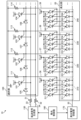
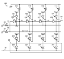
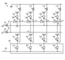
- FIG. 1 is a diagram showing a configuration example of a light emitting device according to an embodiment of the present disclosure.
- FIG. 1 is a block diagram showing a configuration example of the light emitting device 10.
- the light-emitting device 10 is a device for irradiating a subject with light, and is assumed to be used as a distance measuring device 701, which will be described later with reference to FIG.
- a light-emitting portion 20 is also shown in the figure.
- the light emitting unit 20 includes a plurality of light emitting elements and emits light for irradiating an object such as a subject.
- the light-emitting unit 20 in the figure represents an example in which a laser diode is used as a light-emitting element.
- the light emitting section 20 in the figure includes light emitting elements 211 to 214, 221 to 224, 231 to 234 and 241 to 244.
- the light emitting elements 211 to 214, 221 to 224, 231 to 234 and 241 to 244 constitute light emitting element groups 210, 220, 230 and 240, respectively.
- the respective light emitting elements forming the light emitting element group 210 and the like are simultaneously driven to emit light.
- the cathodes of the light emitting elements 211 to 214, 221 to 224, 231 to 234 and 241 to 244 are connected to the signal line 35.
- Anodes of the light emitting elements 211 to 214, 221 to 224, 231 to 234 and 241 to 244 are connected to cathodes of the drive thyristors 311 to 314, 321 to 324, 331 to 334 and 341 to 344, respectively.
- the drive thyristors 311 to 314, 321 to 324, 331 to 334 and 341 to 344 are arranged in the light emitting element 211 and the like as described above.
- the driving thyristor 311 or the like is connected to the light emitting element 211 or the like and conducts itself, thereby causing a light emission current to flow through the light emitting element 211 or the like for driving.
- the drive thyristors 311 to 314, 321 to 324, 331 to 334, and 341 to 344 correspond to the light emitting element groups 210, 220, 230, and 240, respectively, and simultaneously drive the light emitting elements included in the respective light emitting element groups. drive.
- the driving thyristors 311 to 314, 321 to 324, 331 to 334, and 341 to 344 shown in FIG. can be done. Details of the drive thyristor 311 and the like will be described later.
- Anodes of the driving thyristors 311 to 314, 321 to 324, 331 to 334 and 341 to 344 are commonly connected to the power supply line Vcc2.
- Gates of the drive thyristors 311 to 314 are connected to the signal line 36 .
- Gates of the drive thyristors 321 to 324 are commonly connected to the signal line 37 .
- Gates of the drive thyristors 331 to 334 are commonly connected to the signal line 38 .
- Gates of the drive thyristors 341 to 344 are commonly connected to the signal line 39 .
- a conduction signal for conducting the drive thyristor 311 and the like is output from the selector 100 to the signal lines 36 to 39 .
- the power line Vcc2 is a power line for supplying a power voltage to the light emitting element 211 and the like.
- the selection unit 100 selects a drive thyristor.
- a selection unit 100 shown in the figure selects each drive thyristor group such as the drive thyristors 311 to 314 corresponding to the light emitting element group and outputs a conduction signal.
- the selection unit 100 includes selection thyristors 101-104, diodes 105-108, and resistors 111-114.
- Anodes of the selected thyristors 101 to 104 are commonly connected to the power supply line Vcc1.
- the gates of the select thyristors 101-104 are connected to signal lines 36-39, respectively.
- the sources of select thyristors 101 and 103 are commonly connected to one end of resistor 31 .
- the other end of resistor 31 is connected to signal line 33 .
- the sources of select thyristors 102 and 104 and the anode of diode 105 are commonly connected to one end of resistor 32 .
- the other end of resistor 32 is connected to signal line 34 .
- the cathode of diode 105 is connected to signal line 36 .
- the diode 106 has an anode connected to the signal line 36 and a cathode connected to the signal line 37 .
- the diode 107 has an anode connected to the signal line 37 and a cathode connected to the signal line 38 .
- Diode 108 has an anode connected to signal line 38 and a cathode connected to signal line 39 .
- One end of the resistor 111 is connected to the signal line 36 and the other end is grounded.
- One end of the resistor 112 is connected to the signal line 37 and the other end is grounded.
- One end of the resistor 113 is connected to the signal line 38 and the other end is grounded.
- One end of the resistor 114 is connected to the signal line 39 and the other end is grounded.
- the power line Vcc1 is a power line that supplies a power voltage to the selection unit 100 .
- the selection thyristors 101 to 104 output conduction signals for the drive thyristor 311 and the like.
- the selected thyristors 101 to 104 output the gate voltage as the conduction signal when they themselves become conductive.
- a thyristor made of a GaAs compound semiconductor can be used for the selection thyristor 101 or the like, and a p-gate thyristor can be used.
- the diodes 105 to 108 transmit gate voltages for conducting the selected thyristor 101 and the like.
- a diode made of a GaAs compound semiconductor can be used for the diode 105 and the like.
- the resistors 111 to 114 are resistors that transmit the ground potential to the gates of the selected thyristor 101 and the like.
- Signal lines 33 and 34 are signal lines for transmitting transfer signals (transfer signals ⁇ 1 and ⁇ 2) from the transfer signal generator 130 . These transfer signals drive the selector 100 .
- the selector 100 has a drive period in which one of the selected thyristors 101 to 104 is turned on to output a drive signal to the corresponding drive thyristor 311 or the like, and a transfer period in which the selected thyristors 101 to 104 are selected. alternately repeat.
- the gate voltage is sequentially transferred, and the selected thyristors 101 to 104, among the selected thyristors 101 to 104, are driven to sequentially shift the position of the selected thyristor 101 and the like. Details of the operation of the selection unit 100 will be described later.
- the transfer signal generation unit 130 generates the transfer signal described above.
- a transfer signal generation unit 130 in the figure generates transfer signals ⁇ 1 and ⁇ 2 and outputs them to signal lines 33 and 34, respectively. Details of the transfer signals ⁇ 1 and ⁇ 2 will be described later.
- the light emission current supply unit 170 supplies the light emission current to the light emitting element 211 and the like during the driving period described above.
- the light emission current supply unit 170 supplies the light emission current during the light emission period during which the light emitting elements 211 and the like emit light, and stops the supply of the light emission current during the non-light emission periods during which the light emitting elements 211 and the like stop emitting light.
- the light emitting current supply unit 170 can alternately repeat these light emitting periods and non-light emitting periods.
- the light emission current supply unit 170 can supply the light emission current by applying a pulsed driving signal to the light emitting element 211 or the like. This drive signal is applied via the signal line 35 .
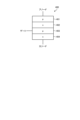
- FIG. 2 is a diagram showing a configuration example of a thyristor according to an embodiment of the present disclosure.
- This figure is a diagram showing a configuration example of a thyristor 400 that can be applied as the driving thyristor 311 or the like or the selection thyristor 101 or the like.
- the thyristor 400 is a semiconductor element formed by joining an n-type semiconductor 404, a p-type semiconductor 403, an n-type semiconductor 402, and a p-type semiconductor 401 in order. Also, these n-type semiconductor 404, p-type semiconductor 403, n-type semiconductor 402 and p-type semiconductor 401 can be composed of GaAs compound semiconductors.
- An anode electrode is arranged on the p-type semiconductor 401 and a cathode electrode is arranged on the n-type semiconductor 404 .
- a gate electrode is arranged on the p-type semiconductor 403 .
- a thyristor 400 is called a p-gate thyristor.
- the threshold voltage of the gate voltage is approximately 1.5V.
- a holding current is defined as the minimum current that maintains the conducting state in the thyristor 400 that has transitioned to the conducting state. To transition the conducting thyristor 400 to the non-conducting state, the current flowing between the anode and cathode must be less than the holding current.
- a thyristor in which a gate electrode is arranged on the n-type semiconductor 402 in the figure is called an n-gate thyristor.
- this n-gate thyristor by applying a gate voltage that becomes a low potential with respect to the anode. can be made conductive.
- Such an n-gate thyristor can also be applied to the drive thyristor 311 and the like, the selection thyristor 101 and the like. In that case, the anode and cathode voltages need to be reversed.
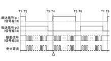
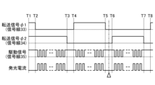
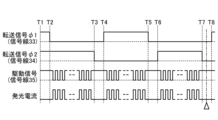
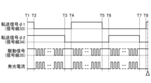
- FIGS. 10A and 10B are diagrams illustrating an example of a driving method according to embodiments of the present disclosure.
- 3A-10A are timing diagrams representing drive waveforms.
- 3B-10B are circuit diagrams representing the state of the circuit according to the timing diagrams of FIGS. 3A-10A.
- transfer signal ⁇ 1" and “transfer signal ⁇ 2” represent binarized waveforms of transfer signal ⁇ 1 and transfer signal ⁇ 2 transmitted via signal lines 33 and 34, respectively.
- a “driving signal” represents the waveform of the driving signal transmitted through the signal line 35 .
- light emission current represents the waveform of the light emission current flowing through the light emitting element 211 and the like.
- the dashed horizontal line represents a potential of 0V.
- the power supply voltage of the power supply lines Vcc1 and Vcc2 is assumed to be 3.3V. Note that in FIGS. 3A-10A, the triangle represents the current position in the timing diagram.
- 3B to 10B are simplified circuits of the circuit in FIG. 1 and show examples of the light emitting section 20 having the light emitting elements 211, 221, 231 and 241.
- FIG. In this case drive thyristors 311, 321, 331 and 341 are arranged.
- the forward voltage drop across diode 105 etc. is assumed to be 1.5V.
- the threshold of the gate voltage of the selected thyristor 101 etc. is assumed to be 1.5V.
- the forward voltage drop of the selected thyristor 101 etc. is assumed to be 2.0V.
- the light emission threshold voltage of the laser diode that constitutes the light emitting element 211 and the like is 2.5V.
- T1 in FIG. 3A represents the initial state.
- 3.3V is applied to the transfer signals ⁇ 1 and ⁇ 2.
- 3.3 V is applied as a drive signal.
- FIG. 3B 3.3V is applied to signal lines 33 and 34 .
- This voltage is transferred by diode 105 and the gate of selected thyristor 101 rises to 1.8V.
- the drive signal ⁇ 1 of 3.3 V is applied to the cathode through the resistor 31, the selected thyristor 101 remains non-conducting.
- the gate voltage of the selected thyristor 101 is transmitted to the gate of the selected thyristor 102 through the diode 106 and rises to 0.3V.
- the transfer signal ⁇ 1 becomes 0V. Since the gate voltage is 1.5V, the selected thyristor 101 becomes conductive. Then, since the cathode current of the selected thyristor 101 flows through the resistor 31, the terminal voltage of the resistor 31 rises and the cathode voltage of the selected thyristor 101 rises from 0V to 1.3V. Further, the conduction of the selected thyristor 101 raises the gate voltage of the selected thyristor 101 to 3.3V. This gate voltage is transmitted by diode 106 and the gate voltage of selected thyristor 102 becomes 1.8V. However, since the cathode voltage of the selected thyristor 102 is 3.3V, the selected thyristor 102 remains non-conducting.
- the driving thyristor 311 is selected by the selection thyristor 101 from T2 to T3.
- a gate voltage of 3.3V is applied as a conduction signal to the gate of drive thyristor 311, causing drive thyristor 311 to become conductive.
- a voltage of 0 V is applied as a drive signal in this state, a light emission current flows through the light emitting element 211 via the drive thyristor 311 .
- This figure shows an example in which a pulse train driving signal is applied. A light emission current flows in a pulse shape according to the driving signal of the pulse train.
- the selected thyristor 101 remains conductive because the transfer signal ⁇ 1 is 0V. Also, the transfer signal ⁇ 2 becomes 0V. Since the gate voltage is 1.8V, the selected thyristor 102 becomes conductive. Then, since the cathode current of the selected thyristor 102 flows through the resistor 32, the terminal voltage of the resistor 32 rises and the cathode voltage of the selected thyristor 102 rises from 0V to 1.3V. Also, the conduction of the selected thyristor 102 raises the gate voltage of the selected thyristor 102 to 3.3V.
- This gate voltage is transmitted by the diode 107 and the gate voltage of the selected thyristor 103 becomes 1.8V. However, since the cathode voltage of the selected thyristor 103 is 1.3V, the selected thyristor 102 remains non-conducting.
- the transfer signal ⁇ 1 becomes 3.3V.
- the conduction state of the selected thyristor 101 is stopped.
- the selected thyristor 102 remains conductive. Since the cathode voltage is 3.3V, the selected thyristor 103 remains non-conducting.
- a gate voltage of 3.3 V is applied as a conduction signal to the gate of the drive thyristor 321, and the drive thyristor 321 becomes conductive.
- a drive signal of 0 V is applied in this state, a light emission current flows through the light emitting element 221 via the drive thyristor 321 .
- the selected thyristor 102 remains conductive because the transfer signal ⁇ 2 is 0V. Also, the transfer signal ⁇ 1 becomes 0V. Since the gate voltage is 1.8V, the selected thyristor 103 becomes conductive. Then, since the cathode current of the selected thyristor 103 flows through the resistor 31, the terminal voltage of the resistor 31 rises and the cathode voltage of the selected thyristor 103 rises from 0V to 1.3V. Further, the conduction of the selected thyristor 103 raises the gate voltage of the selected thyristor 103 to 3.3V.
- This gate voltage is transmitted by the diode 108 and the gate voltage of the selected thyristor 104 becomes 1.8V. However, since the cathode voltage of the selected thyristor 104 is 1.3V, the selected thyristor 104 remains non-conducting.
- the transfer signal ⁇ 2 becomes 3.3V.
- the conduction state of the selected thyristor 102 is stopped.
- the selected thyristor 103 remains conductive. Since the cathode voltage is 3.3V, the selected thyristor 104 remains non-conducting.
- a gate voltage of 3.3 V is applied as a conduction signal to the gate of the driving thyristor 331, and the driving thyristor 331 becomes conductive.
- a drive signal of 0 V is applied in this state, a light emission current flows through the light emitting element 231 via the drive thyristor 331 .
- the selected thyristor 103 remains conductive because the transfer signal ⁇ 1 is 0V. Also, the transfer signal ⁇ 1 becomes 0V. Since the gate voltage is 1.8V, the selected thyristor 104 becomes conductive. Then, the cathode voltage of the selected thyristor 104 rises from 0V to 1.3V. Also, the conduction of the selected thyristor 104 raises the gate voltage of the selected thyristor 104 to 3.3V.
- the transfer signal ⁇ 1 becomes 3.3V.
- the conduction state of the selected thyristor 103 is stopped.
- the selected thyristor 104 remains conductive.
- a gate voltage of 3.3V is applied as a conduction signal to the gate of drive thyristor 341, causing drive thyristor 341 to become conductive.
- a drive signal of 0 V is applied in this state, a light emission current flows through the light emitting element 241 via the drive thyristor 341 .
- the light emitting unit 20 is driven by the above procedure.
- the periods T1 to T2, T3 to T4, T5 to T6, and T7 to T8 correspond to the transfer periods.
- the positions of the selected thyristors 101 to 104 which are to be conductive during this selection period are shifted to the right in FIG.
- periods T2 to T3, T4 to T5, and T6 to T7 correspond to drive periods.
- one of the drive thyristors 311, 321, 331 and 341 is selected to be in a conductive state.
- a period during which the light emitting elements 211 and the like emit light is called a light emitting period, and a period during which the light emitting elements 211 and the like stop emitting light is called a non-light emitting period.
- the light emission current supply unit 170 supplies a current that alternately repeats the light emission period and the non-light emission period during the drive period.
- the same conduction current flows in the selection thyristor 101 and the like for selecting the drive thyristor 311 and the like in the transfer period and the drive period.
- the light-emitting device 10 of the first embodiment of the present disclosure is different from the light-emitting device 10 having the basic configuration described above in that the conduction current of the selected thyristor 101 and the like is adjusted during the drive period.
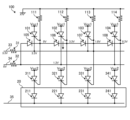
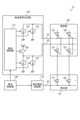
- FIG. 11 is a diagram illustrating a configuration example of a light emitting device according to the first embodiment of the present disclosure; This figure, like FIG. 1, is a block diagram showing a configuration example of the light emitting device 10. As shown in FIG. The light emitting device 10 in FIG. 11 differs from the light emitting device 10 in FIG. 1 in the configuration of the transfer signal ⁇ 1. Also, the resistors 31 and 32 are eliminated in the light emitting device 10 of FIG. Note that the description of the selection unit 100 and the light emission unit 20 in the figure is simplified.
- the transfer signal generation unit 130 in the same figure includes a transfer control unit 131, constant current circuits 132 to 135, and a MOS transistor 136.
- a p-channel MOS transistor can be used for MOS transistor 136 .
- Sinking terminals of the constant current circuits 132 and 133 are commonly connected to the signal line 33 .
- the discharge side terminals of the constant current circuits 132 and 133 are grounded.
- a control signal from the transfer control unit 131 is input to the control terminals of the constant current circuits 132 and 133 .
- the suction side terminals of the constant current circuits 134 and 135 and the drain of the MOS transistor 136 are commonly connected to the signal line 34 .
- the source of MOS transistor 136 is connected to power supply line Vcc1.
- the discharge side terminals of the constant current circuits 134 and 135 are grounded.
- a control signal from the transfer control unit 131 is input to the control terminals of the constant current circuits 134 and 135 and the gate of the MOS transistor 136 .
- the constant current circuits 132 to 135 are circuits that pass constant current.
- the constant current circuits 133 and 135 are circuits that pass a constant current of a lower value compared to the constant current circuits 132 and 134 . Further, the constant current circuits 132 to 135 stop supplying constant current based on the control signal from the transfer control section 131 .
- the constant current circuits 132 and 134 By switching between the constant current circuits 132 and 134 and the constant current circuits 133 and 135, the currents flowing through the signal lines 33 and 34 can be adjusted, and the cathode voltage of the selected thyristor 101 and the like can be changed.
- the current supplied by the constant current circuits 133 and 135 can be based on the holding current of the selected thyristor 101 or the like.
- the constant current circuits 133 and 135 can adopt a configuration that allows a current twice as large as the holding current of the selected thyristor 101 or the like to flow, for example.
- the MOS transistor 136 is a MOS transistor that supplies power supply voltage to the signal line 34 .
- the MOS transistor 136 applies a power supply voltage of 3.3V to the signal line 34 while the supply of constant current from the constant current circuits 134 and 135 is stopped.
- the transfer signal generator 130 in the same drawing is an example of the current adjuster described in the scope of claims.
- FIG. 12 is a diagram illustrating an example of a driving method according to the first embodiment of the present disclosure.
- This figure like FIG. 3A, is a timing diagram showing drive waveforms.
- “current of selected thyristor 101 ” represents the current waveform of selected thyristor 101 .
- “Current of selected thyristor 102 ” represents the current waveform of selected thyristor 102 . Otherwise, the same notation as in FIG. 3A is used.
- the constant current circuits 132 to 135 stop supplying constant current. Also, the MOS transistor 136 is turned on. As a result, the transfer signal ⁇ 2 becomes 3.3V. On the other hand, the transfer signal ⁇ 1 becomes 3.3 V due to the action of the selected thyristor 101 .
- a period from T0 to T1 corresponds to a reset period.
- the constant current circuit 132 starts supplying a constant current (1 mA).
- the voltage of the transfer signal ⁇ 1 becomes 0 V, and the selected thyristor 101 becomes conductive.
- a current of 1 mA flows through the selected thyristor 101 .
- the selected thyristor 101 is selected during this period. Note that the MOS transistor 136 can be rendered non-conductive during the period after T2.
- the selected thyristor 101 maintains the conducting state.
- the constant current circuit 132 is controlled to be turned off, and the constant current circuit 133 supplies a constant current (0.2 mA).
- the voltage of the transfer signal ⁇ 1 becomes 1.5 V, and the current of the selected thyristor 101 becomes 0.2 mA. Since the selected thyristor 101 maintains the conducting state, the corresponding driving thyristor 311 is conducting, and a light emitting current corresponding to the driving signal flows through the light emitting element 211 .
- the constant current circuit 133 keeps supplying constant current (0.2 mA). Also, the selected thyristor 102 is turned on, and the constant current circuit 134 supplies a constant current (1 mA). As a result, a current of 0.2 mA flows through the selected thyristor 101 and a current of 1 mA flows through the selected thyristor 102 .
- the selected thyristor 101 is in a non-conducting state and the selected thyristor 102 is in a conducting state.
- the constant current circuits 132 and 133 stop supplying the constant current, and the constant current circuit 135 supplies the constant current (0.2 mA).
- the voltage of transfer signal ⁇ 2 becomes 1.5 V
- the current of selected thyristor 102 becomes 0.2 mA. Since the selected thyristor 102 maintains the conducting state, the corresponding driving thyristor 321 is conducting, and a light emitting current corresponding to the driving signal flows through the light emitting element 221 .
- the voltage of the transfer signal ⁇ 1 becomes 3.3V, and the current of the selected thyristor 101 becomes 0A.
- the constant current circuit 135 keeps supplying a constant current (0.2 mA), and a current of 0.2 mA flows through the selected thyristor 102. Also, the constant current circuit 132 starts supplying a constant current (1 mA). As a result, the voltage of the transfer signal ⁇ 1 becomes 0 V, and the selected thyristor 103 (not shown) is turned on. A current of 1 mA flows through the selected thyristor 103 .
- the current is similarly adjusted in the selected thyristors 103 and 104 as well. It is possible to reduce the current of the selected thyristor 101 and the like during the drive period. On the other hand, during the transfer period, by allowing a relatively large current to flow through the selected thyristor 101 or the like, it is possible to shorten the transition time between the conducting state and the non-conducting state.
- FIG. 13 is a diagram illustrating another configuration example of the light emitting device according to the first embodiment of the present disclosure; This figure is a block diagram showing a configuration example of the light emitting device 10, like FIG.
- the light-emitting device 10 in FIG. 11 differs from the light-emitting device 10 in FIG. 11 in that the current is adjusted by switching resistors instead of the constant current circuit 132 and the like.
- the transfer signal generation section 130 in the figure includes a transfer control section 131, amplifiers 140 and 141, switch elements 142 and 144, and resistors 146 to 149.
- the output of amplifier 140 is connected to one end of switch elements 142 and 143 .
- the other ends of switch elements 142 and 143 are connected to signal line 33 via resistors 146 and 147, respectively.
- a control signal from the transfer control unit 131 is transmitted to the input of the amplifier 140 and the control inputs of the switch elements 142 and 143 .
- the output of amplifier 141 is connected to one end of switch elements 144 and 145 .
- the other ends of switch elements 144 and 145 are connected to signal line 34 via resistors 148 and 149, respectively.
- a control signal from the transfer control unit 131 is transmitted to the input of the amplifier 141 and the control inputs of the switch elements 144 and 145 .
- the amplifiers 140 and 141 output signals of a predetermined voltage under the control of the transfer control section 131.
- Amplifiers 140 and 141 in the same figure can output an output voltage of 3.3V or 0V.
- a sink current is supplied.
- the resistors 146 to 149 are resistors that limit the current flowing through the signal lines 33 and 34 .
- Resistors 147 and 149 can be configured with higher resistance values than resistors 146 and 148 .
- the switch elements 142 to 145 are elements that become conductive and non-conductive based on control signals applied to control terminals.
- the switch element 142 When the switch element 142 is turned on, the output of the amplifier 140 is connected to the signal line 33 via the resistor 146 with a relatively low value. Therefore, a large current can flow through the selected thyristor 101 and the like.
- the switch element 143 when the switch element 143 is turned on, the output of the amplifier 140 is connected to the signal line 33 via the resistor 147 having a relatively high value. Therefore, a relatively small current can flow through the selected thyristor 101 and the like.
- the light emitting device 10 of the first embodiment of the present disclosure can reduce power consumption by reducing the current of the selected thyristor 101 and the like during the driving period.
- the light emitting device 10 of the first embodiment described above reduces the conduction current of the selected thyristor 101 and the like during the drive period.
- the light-emitting device 10 of the second embodiment of the present disclosure is different from the light-emitting device 10 of the above-described first embodiment in that the selected thyristor 101 and the like are brought into a non-conducting state during the drive period.
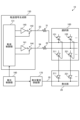
- FIG. 14 is a diagram illustrating a configuration example of a light emitting device according to a second embodiment of the present disclosure; This figure is a block diagram showing a configuration example of the light emitting device 10, like FIG.
- the light-emitting device 10 of FIG. 11 differs from the light-emitting device 10 of FIG. 11 in that resistors 31 and 32 are connected to signal lines 33 and 34 .
- the transfer signal generator 130 in the figure includes a transfer controller 131, amplifiers 140 and 141, and switch elements 142 and 144.
- the output of amplifier 140 is connected to signal line 33 via switch element 142 .
- a control signal from the transfer control unit 131 is input to the input of the amplifier 140 and the control input of the switch element 142 .
- the output of amplifier 141 is connected to signal line 34 via switch element 143 .
- a control signal from the transfer control unit 131 is input to the input of the amplifier 141 and the control input of the switch element 144 .
- a switch element 142 in the figure switches between conduction and non-conduction between the output of the amplifier 140 and the signal line 33 .
- the switch element 144 switches conduction and non-conduction between the output of the amplifier 141 and the signal line 34 .
- FIG. 15 is a diagram illustrating an example of a driving method according to the second embodiment of the present disclosure; Similar to FIG. 12, this figure is a timing chart showing drive waveforms.
- switch element 142 represents the state of the switch element 142.
- switch element 144 represents the state of the switch element 144 .
- the same notation as in FIG. 12 is used.
- an operation of selecting the selection thyristor 101 or the like at a desired position is performed during the transfer period. After that, while the drive thyristors 311 and the like connected to the selected selection thyristors 101 and the like are turned on, the operation of the selection unit 100 is stopped while shifting to the drive period.
- This figure shows an example of selecting the selected thyristor 104 and the driving thyristor 341 .
- the switch elements 142 and 144 are turned on to supply the transfer signals ⁇ 1 and ⁇ 2 to the signal lines 33 and 34, respectively, and the selected thyristor 104 is turned on to supply the conduction signal to the gate of the driving thyristor 341. is applied. As a result, the drive thyristor 341 becomes conductive.
- the switch elements 142 and 144 are brought into a non-conducting state during the drive period of transition to T8. Thereby, the conducting current of the selected thyristor 104 is interrupted.
- the driving thyristor 341 maintains the conducting state, a light emitting current corresponding to the driving signal flows through the light emitting element 241 .
- the drive signal in FIG. 10 supplies a voltage lower than 3.3 V, for example, 1.3 V, during a period in which the light emitting element 241 does not emit light. In this case, the voltage applied to the light emitting elements 241 and the like is less than the light emission threshold voltage, so the light emitting elements 241 and the like do not emit light.
- a conducting current (0.1 A) greater than the holding current flows through the drive thyristor 341 .
- the conductive state of the driving thyristor 311 and the like can be maintained during the driving period.
- the current based on the holding current can be applied to the current that flows through the driving thyristor 341 and the like during the period in which the light emitting element 241 is not emitting light.
- the power consumption of the light emitting device 10 can be reduced because the current of the selected thyristor 101 and the like can be reduced during the drive period.
- FIG. 16 is a diagram illustrating another example of the driving method according to the second embodiment of the present disclosure; Similar to FIG. 15, this figure is a timing chart showing drive waveforms. The driving method in the figure differs from that in FIG. 15 in the driving signal during the driving period.
- a thyristor has the function of maintaining a conducting state for a certain period of time when the conducting current is interrupted.
- the holding current can be reduced. Thereby, the power consumption of the light emitting device 10 can be further reduced.
- the light emitting device 10 of the second embodiment of the present disclosure can reduce power consumption by stopping the operation of the selected thyristor 101 and the like during the drive period.
- FIG. 17 is a diagram illustrating a configuration example of a distance measuring device according to an embodiment of the present disclosure. A distance measuring device 701 shown in FIG. 710.
- the light emitting unit 702 emits light from a plurality of light sources.
- the light emitting unit 702 of this example has light emitting elements 2a by VCSELs (Vertical Cavity Surface Emitting LASER) as respective light sources, and the light emitting elements 2a are arranged in a matrix, for example. are arranged and configured according to a predetermined mode.
- VCSELs Vertical Cavity Surface Emitting LASER
- the drive unit 703 is configured with a power supply circuit 704 for driving the light emitting unit 702 .
- the power supply circuit 704 generates a power supply voltage (driving voltage Vd, which will be described later) for the driving section 703 based on an input voltage (input voltage Vin, which will be described later) from, for example, a battery (not shown) provided in the distance measuring device 701. .
- the driving unit 703 drives the light emitting unit 702 based on the power supply voltage.
- the light emitted from the light emitting unit 702 irradiates the subject S as the distance measurement target through the light emitting side optical system 705 . Reflected light from the subject S of the light irradiated in this way is incident on the light receiving surface of the light receiving unit 707 via the light receiving side optical system 706 .
- the light receiving unit 707 is, for example, a light receiving element such as a CCD (Charge Coupled Device) sensor or a CMOS (Complementary Metal Oxide Semiconductor) sensor. It receives light, converts it to an electrical signal, and outputs it. In addition, the light receiving unit 707 performs, for example, CDS (Correlated Double Sampling) processing, AGC (Automatic Gain Control) processing, etc. on an electrical signal obtained by photoelectrically converting the received light, and further performs A/D (Analog/Digital ) perform the conversion process. Then, the signal as digital data is output to the signal processing section 8 in the subsequent stage.
- CDS Correlated Double Sampling
- AGC Automatic Gain Control
- the light receiving unit 707 of this example outputs the frame synchronization signal Fs to the driving unit 703 . Accordingly, the drive unit 703 can cause the light emitting element 2a in the light emitting unit 702 to emit light at a timing corresponding to the frame period of the light receiving unit 707.
- FIG. 7
- the signal processing unit 8 is configured as a signal processing processor such as a DSP (Digital Signal Processor).
- a signal processing unit 708 performs various kinds of signal processing on the digital signal input from the light receiving unit 707 .
- the control unit 709 includes, for example, a microcomputer having a CPU (Central Processing Unit), ROM (Read Only Memory), RAM (Random Access Memory), etc., or an information processing device such as a DSP. It controls the driving unit 703 for controlling the operation and controls the light receiving operation of the light receiving unit 707 .
- a microcomputer having a CPU (Central Processing Unit), ROM (Read Only Memory), RAM (Random Access Memory), etc., or an information processing device such as a DSP. It controls the driving unit 703 for controlling the operation and controls the light receiving operation of the light receiving unit 707 .
- the control unit 709 has a function as a distance measurement unit 709a.
- the distance measuring unit 709a measures the distance to the subject S based on a signal input via the signal processing unit 708 (that is, a signal obtained by receiving reflected light from the subject S).
- the distance measuring unit 709a of this example measures the distance of each part of the subject S in order to enable the three-dimensional shape of the subject S to be specified. A specific method of distance measurement in the distance measurement device 701 will be described later.
- a temperature detection unit 710 detects the temperature of the light emitting unit 702 .
- the temperature detection unit 710 for example, a configuration that detects temperature using a diode can be adopted.
- the temperature information detected by the temperature detection unit 710 is supplied to the driving unit 703, which enables the driving unit 703 to drive the light emitting unit 702 based on the temperature information.
- [Range measurement method] 18A and 18B are diagrams representing an example of a ranging method according to embodiments of the present disclosure.
- a ranging method in the ranging device 701 for example, a ranging method based on the STL (Structured Light) method or the ToF (Time of Flight) method can be adopted.
- STL Structured Light
- ToF Time of Flight
- the STL method is a method of measuring the distance based on an image of the subject S irradiated with light having a predetermined bright/dark pattern such as a dot pattern or grid pattern.
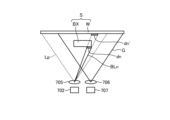
- FIG. 18 is an explanatory diagram of the STL method.
- the subject S is irradiated with pattern light Lp having a dot pattern as shown in FIG. 18A, for example.
- the pattern light Lp is divided into a plurality of blocks BL, and each block BL is assigned a different dot pattern (a dot pattern is prevented from overlapping between blocks B).
- FIG. 18B is an explanatory diagram of the principle of distance measurement of the STL method.
- the wall W and the box BX placed in front of it are the subject S, and the subject S is irradiated with the pattern light Lp.
- “G” in the drawing schematically represents the angle of view of the light receiving unit 707 .
- “BLn” in the drawing means light of a certain block BL in the pattern light Lp
- “dn” means the dot pattern of the block BLn projected on the received light image by the light receiving unit 707 .
- the dot pattern of the block BLn appears at the position of "dn'" in the received light image. That is, the position where the pattern of the block BLn appears in the received light image differs between when the box BX exists and when the box BX does not exist. Specifically, pattern distortion occurs.
- the STL method is a method that obtains the shape and depth of the subject S by utilizing the fact that the irradiated pattern is distorted by the object shape of the subject S. Specifically, this method obtains the shape and depth of the object S from the distortion of the pattern.
- the light receiving unit 707 for example, an IR (Infrared: infrared) light receiving unit using a global shutter method is used.
- the distance measuring unit 709a controls the driving unit 703 so that the light emitting unit 702 emits pattern light, and detects pattern distortion in the image signal obtained through the signal processing unit 708. , to calculate the distance based on how the pattern is distorted.
- the ToF method measures the distance to the object by detecting the flight time (time difference) of the light emitted from the light emitting unit 702 and reflected by the object until it reaches the light receiving unit 707. It is a method to
- the distance measuring unit 709a calculates the time difference between the light emitted by the light emitting unit 702 and the light received by the light receiving unit 707 from the time when the light is emitted from the light emitting unit 702 to the time when the light is received by the light receiving unit 707. and the speed of light.
- a so-called indirect ToF (iToF) method phase difference method
- a light receiving unit capable of receiving IR for example, is used as the light receiving unit 707 .
- the light emitting device 10 shown in FIG. 11 etc. can be used for the light emitting section 702 shown in FIG. Note that the electrical signal output by the light receiving unit 707 corresponds to the light reception signal.
- the light emitting device 10 includes a plurality of light emitting elements (light emitting element 211, etc.), a plurality of drive thyristors (drive thyristor 311, etc.), a selection section 100, a light emission current supply section 170, a current adjustment section (transfer signal generation section 130 ) and
- the drive thyristor is arranged for each of the plurality of light emitting elements, and when it becomes conductive, a light emitting current flows through the light emitting elements to drive the light emitting elements.
- the selection unit 100 includes a plurality of selection thyristors (selection thyristors 101, etc.) that are arranged for each of the plurality of driving thyristors and output a conduction signal that makes the driving thyristors conductive when the selection unit 100 is in conduction.
- a transfer period for sequentially selecting a plurality of driving thyristors and a driving period for driving the light-emitting element by the selected driving thyristor are alternately repeated by sequentially shifting the position of the selected thyristor to be turned on.
- the light emission current supply unit 170 supplies light emission current to the light emitting element through the selected drive thyristor during the drive period.
- the current adjustment unit (transfer signal generation unit 130) supplies the conduction current of the selected thyristor and adjusts the conduction current of the selected thyristor during the driving period. By adjusting the current of the selected thyristor, the power consumption of the light emitting device 10 can be reduced.
- the current adjustment unit may adjust the conducting current based on the holding current of the selected thyristor. This can prevent the selected thyristor from transitioning to a non-conducting state.
- the light emission current supply unit 170 may supply the light emission current during the light emission period during which the light emitting element emits light, and stop supplying the light emission current during the non-light emission period during which the light emitting element stops emitting light. Thereby, pulsed light emission can be obtained.
- the light emission current supply unit 170 may alternately repeat the light emission period and the non-light emission period. This makes it possible to obtain light emission in the form of a pulse train.
- the conduction signal may be commonly output to a plurality of driving thyristors of the light emitting element group arranged for each element group. Thereby, a plurality of light emitting elements can be driven in common.
- the distance measuring device 701 has a light emitting device 10, a light receiving section 707, and a distance measuring section 709a.
- the light emitting device 10 includes a plurality of light emitting elements (light emitting element 211, etc.), a plurality of drive thyristors (drive thyristor 311, etc.), a selection section 100, a light emission current supply section 170, a current adjustment section (transfer signal generation section 130 ).
- the drive thyristor is arranged for each of the plurality of light emitting elements, and when it becomes conductive, a light emitting current flows through the light emitting elements to drive the light emitting elements.
- the selection unit 100 includes a plurality of selection thyristors (selection thyristors 101, etc.) that are arranged for each of the plurality of driving thyristors and output a conduction signal that makes the driving thyristors conductive when the selection unit 100 is in conduction.
- a transfer period for sequentially selecting a plurality of driving thyristors and a driving period for driving the light-emitting element by the selected driving thyristor are alternately repeated by sequentially shifting the position of the selected thyristor to be turned on.
- the light emission current supply unit 170 supplies light emission current to the light emitting element through the selected drive thyristor during the drive period.
- the current adjustment unit (transfer signal generation unit 130) supplies the conduction current of the selected thyristor and adjusts the conduction current of the selected thyristor during the drive period.
- the light-receiving unit 707 receives light reflected by the object from the light-emitting element and generates a light-receiving signal.
- the distance measuring unit 709a measures the distance to the object based on the received light signal. By adjusting the current of the selected thyristor, the power consumption of the distance measuring device 701 can be reduced.
- the light emitting device 10 includes a plurality of light emitting elements (light emitting elements 211, etc.), a plurality of drive thyristors (drive thyristor 311, etc.), a selection section 100, a light emission current supply section 170, and a control section.
- the drive thyristor is arranged for each of the plurality of light emitting elements, and when it becomes conductive, a light emitting current flows through the light emitting elements to drive the light emitting elements.
- the selection unit 100 includes a plurality of selection thyristors (selection thyristors 101, etc.) that are arranged for each of the plurality of driving thyristors and output a conduction signal that makes the driving thyristors conductive when the selection unit 100 is in conduction.
- a transfer period for sequentially selecting a plurality of driving thyristors and a driving period for driving the light-emitting element by the selected driving thyristor are alternately repeated by sequentially shifting the position of the selected thyristor to be turned on.
- the light emission current supply unit 170 supplies light emission current to the light emitting element through the selected drive thyristor during the drive period.
- the control unit performs control to stop the conduction current supply to the selected thyristor during the driving period. By stopping the supply of conduction current to the selected thyristor during the driving period, the power consumption of the light emitting device 10 can be reduced.
- the light emission current supply unit 170 may supply the light emission current during the light emission period during which the light emitting element emits light, and stop supplying the light emission current during the non-light emission period during which the light emitting element stops emitting light. Thereby, pulsed light emission can be obtained.
- the light emission current supply unit 170 may alternately repeat the light emission period and the non-light emission period. This makes it possible to obtain light emission in the form of a pulse train.
- the light emission current supply unit 170 may supply a current based on the holding current of the drive thyristor during the non-light emission period. This can prevent the driving thyristor from transitioning to a non-conducting state.
- the conduction signal may be commonly output to a plurality of driving thyristors of the light emitting element group arranged for each element group. Thereby, a plurality of light emitting elements can be driven in common.
- the distance measuring device 701 has a light emitting device 10, a light receiving section 707, and a distance measuring section 709a.
- the light emitting device 10 includes a plurality of light emitting elements (light emitting element 211, etc.), a plurality of drive thyristors (drive thyristor 311, etc.), a selection section 100, a light emission current supply section 170, and a control section.
- the drive thyristor is arranged for each of the plurality of light emitting elements, and when it becomes conductive, a light emitting current flows through the light emitting elements to drive the light emitting elements.
- the selection unit 100 includes a plurality of selection thyristors (selection thyristors 101, etc.) that are arranged for each of the plurality of driving thyristors and output a conduction signal that makes the driving thyristors conductive when the selection unit 100 is in conduction.
- a transfer period for sequentially selecting a plurality of driving thyristors and a driving period for driving the light-emitting element by the selected driving thyristor are alternately repeated by sequentially shifting the position of the selected thyristor to be turned on.
- the light emission current supply unit 170 supplies light emission current to the light emitting element through the selected drive thyristor during the drive period.
- the control unit performs control to stop the conduction current supply to the selected thyristor during the driving period.
- the light-receiving unit 707 receives light reflected by the object from the light-emitting element and generates a light-receiving signal.
- the distance measuring unit 709a measures the distance to the object based on the received light signal. By stopping the supply of conduction current to the selected thyristor during the driving period, the power consumption of the distance measuring device 701 can be reduced.
- the present technology can also take the following configuration. (1) a plurality of light emitting elements; a plurality of drive thyristors that are arranged for each of the plurality of light emitting elements and that are electrically connected to drive the light emitting elements by causing a light emission current to flow therethrough; A plurality of selection thyristors are provided for each of the plurality of driving thyristors and output a conduction signal for making the driving thyristors conductive when the driving thyristors themselves are turned on.
- a selection unit that alternately repeats a transfer period for sequentially selecting the plurality of driving thyristors by sequentially shifting the positions of the driving thyristors and a driving period for causing the selected driving thyristors to drive the light emitting elements; a light emission current supply unit that supplies the light emission current to the light emitting element via the selected drive thyristor during the drive period; and a current adjustment unit that supplies the conduction current of the selected thyristor and adjusts the conduction current of the selected thyristor during the drive period.
- the light emission current supply unit supplies the light emission current during a light emission period during which the light emitting element emits light, and stops supplying the light emission current during a non-light emission period during which the light emitting element stops emitting light. ).
- the drive thyristor is arranged for each of the light emitting elements of the plurality of light emitting element groups;
- the light emitting device according to any one of (1) to (4), wherein the selection thyristor is arranged for each light emitting element group and commonly outputs the conduction signal to the driving thyristors of the light emitting element group.
- (6) a plurality of light emitting elements; a plurality of drive thyristors that are arranged for each of the plurality of light emitting elements and that are electrically connected to drive the light emitting elements by causing a light emission current to flow therethrough;
- a plurality of selection thyristors are provided for each of the plurality of driving thyristors and output a conduction signal for making the driving thyristors conductive when the driving thyristors themselves are turned on.
- a selection unit that alternately repeats a transfer period for sequentially selecting the plurality of driving thyristors by sequentially shifting the positions of the driving thyristors and a driving period for causing the selected driving thyristors to drive the light emitting elements; a light emission current supply unit that supplies the light emission current to the light emitting element via the selected drive thyristor during the drive period; a light emitting device comprising: a current adjustment unit that supplies the conduction current of the selected thyristor and adjusts the conduction current of the selected thyristor during the drive period; a light-receiving unit that receives light reflected by an object from the light-emitting element and generates a light-receiving signal; a distance measuring unit that measures the distance to the object based on the received light signal.
- a plurality of light emitting elements a plurality of drive thyristors that are arranged for each of the plurality of light emitting elements and that are electrically connected to drive the light emitting elements by causing a light emission current to flow therethrough;
- a plurality of selection thyristors are provided for each of the plurality of driving thyristors and output a conduction signal for making the driving thyristors conductive when the driving thyristors themselves are turned on.
- a selection unit that alternately repeats a transfer period for sequentially selecting the plurality of driving thyristors by sequentially shifting the positions of the driving thyristors and a driving period for causing the selected driving thyristors to drive the light emitting elements; a light emission current supply unit that supplies the light emission current to the light emitting element via the selected drive thyristor during the drive period; and a control unit that controls to stop the supply of conduction current to the selected thyristor during the drive period.
- the light emission current supply unit supplies the light emission current during a light emission period during which the light emitting element emits light, and stops supplying the light emission current during a non-light emission period during which the light emitting element stops emitting light.
- Luminescent device (9) The light-emitting device according to (8), wherein the light-emitting current supply section alternately repeats the light-emitting period and the non-light-emitting period. (10) The light-emitting device according to (8), wherein the light-emitting current supply unit supplies a current based on a holding current of the driving thyristor during the non-light-emitting period.
- the drive thyristor is arranged for each of the light emitting elements of the plurality of light emitting element groups;
- a plurality of light emitting elements (12) a plurality of light emitting elements; a plurality of driving thyristors which are arranged for each of the plurality of light emitting elements and drive the light emitting elements by causing a light emitting current to flow through the light emitting elements when the driving thyristors themselves become conductive;
- a plurality of selection thyristors are provided for each of the plurality of driving thyristors and output a conduction signal for making the driving thyristors conductive when the driving thyristors themselves are turned on.
- a selection unit that alternately repeats a transfer period for sequentially selecting the plurality of driving thyristors by sequentially shifting the positions of the driving thyristors and a driving period for causing the selected driving thyristors to drive the light emitting elements; a light emission current supply unit that supplies the light emission current to the light emitting element via the selected drive thyristor during the drive period; a light-emitting device comprising: a control unit that performs control to stop supply of conduction current to the selected thyristor during the drive period; a light-receiving unit that receives light reflected by an object from the light-emitting element and generates a light-receiving signal; a distance measuring unit that measures the distance to the object based on the received light signal.
Landscapes
- Physics & Mathematics (AREA)
- Engineering & Computer Science (AREA)
- Electromagnetism (AREA)
- General Physics & Mathematics (AREA)
- Radar, Positioning & Navigation (AREA)
- Remote Sensing (AREA)
- Computer Networks & Wireless Communication (AREA)
- Condensed Matter Physics & Semiconductors (AREA)
- Optics & Photonics (AREA)
- Led Devices (AREA)
- Measurement Of Optical Distance (AREA)
- Length Measuring Devices By Optical Means (AREA)
Abstract
Description
1.基本の構成
2.第1の実施形態
3.第2の実施形態
4.測距装置の構成
[発光装置の構成]
図1は、本開示の実施形態に係る発光装置の構成例を示す図である。同図は、発光装置10の構成例を表すブロック図である。この発光装置10は、被写体に光を照射する装置であり、図17において後述する測距装置701に使用する装置を想定したものである。
図2は、本開示の実施形態に係るサイリスタの構成例を示す図である。同図は、駆動サイリスタ311等や選択サイリスタ101等として適用可能なサイリスタ400の構成例を表す図である。サイリスタ400は、n型半導体404、p型半導体403、n型半導体402及びp型半導体401が順に接合されて構成される半導体素子である。また、これらn型半導体404、p型半導体403、n型半導体402及びp型半導体401は、GaAs化合物半導体により構成することができる。
図3A及び3B-図10A及び10Bは、本開示の実施形態に係る駆動方法の一例を示す図である。図3A-図10Aは、駆動波形を表すタイミング図である。また、図3B-図10Bは、図3A-図10Aのタイミング図に応じて回路の状態を表す回路図である。
上述の基本の構成の発光装置10は、駆動サイリスタ311等を選択する選択サイリスタ101等に、転送期間及び駆動期間において同じ導通電流が流れていた。これに対し、本開示の第1の実施形態の発光装置10は、駆動期間における選択サイリスタ101等の導通電流を調整する点で、上述の基本構成の発光装置10と異なる。
図11は、本開示の第1の実施形態に係る発光装置の構成例を示す図である。同図は、図1と同様に、発光装置10の構成例を表すブロック図である。図11の発光装置10は、転送信号φ1の構成が図1の発光装置10と異なる。また、同図の発光装置10では、抵抗31及び32を削除される。なお、同図の選択部100及び発光部20は、記載を簡略化している。
図12は、本開示の第1の実施形態に係る駆動方法の一例を示す図である。同図は、図3Aと同様に、駆動波形を表すタイミング図である。同図において、「選択サイリスタ101の電流」は、選択サイリスタ101の電流波形を表す。「選択サイリスタ102の電流」は、選択サイリスタ102の電流波形を表す。これ以外は、図3Aと同様の表記を使用する。
図13は、本開示の第1の実施形態に係る発光装置の他の構成例を示す図である。同図は、図11と同様に、発光装置10の構成例を表すブロック図である。同図の発光装置10は、定電流回路132等の代わりに抵抗を切り替えることにより電流を調整する点で、図11の発光装置10と異なる。
上述の第1の実施形態の発光装置10は、駆動期間における選択サイリスタ101等の導通電流を削減していた。これに対し、本開示の第2の実施形態の発光装置10は、駆動期間における選択サイリスタ101等を非導通の状態にする点で、上述の第1の実施形態の発光装置10と異なる。
図14は、本開示の第2の実施形態に係る発光装置の構成例を示す図である。同図は、図11と同様に、発光装置10の構成例を表すブロック図である。同図の発光装置10は、信号線33及び34に抵抗31及び32が接続される点で、図11の発光装置10と異なる。
図15は、本開示の第2の実施形態に係る駆動方法の一例を示す図である。同図は、図12と同様に、駆動波形を表すタイミング図である。同図において、「スイッチ素子142」は、スイッチ素子142の状態を表す。「スイッチ素子144」は、スイッチ素子144の状態を表す。これ以外は、図12と同様の表記を使用する。
図16は、本開示の第2の実施形態に係る駆動方法の他の例を示す図である。同図は、図15と同様に、駆動波形を表すタイミング図である。同図の駆動方法は、駆動期間の駆動信号が図15と異なる。
発光装置10を使用する測距装置について説明する。
図17は、本開示の実施形態に係る測距装置の構成例を表す図である。同図の測距装置701は、発光部702、駆動部703、電源回路704、発光側光学系705、受光側光学系706、受光部707、信号処理部708、制御部709、及び温度検出部710を備える。
図18A及び18Bは、本開示の実施形態に係る測距方法の一例を表す図である。測距装置701における測距手法としては、例えばSTL(Structured Light:構造化光)方式やToF(Time of Flight:光飛行時間)方式による測距手法を採用することができる。
発光装置10は、複数の発光素子(発光素子211等)と、複数の駆動サイリスタ(駆動サイリスタ311等)と、選択部100と、発光電流供給部170と、電流調整部(転送信号生成部130)とを有する。駆動サイリスタは、複数の発光素子毎に配置されて自身が導通することにより発光素子に発光電流を流して駆動する。選択部100は、複数の駆動サイリスタ毎に配置されて自身が導通する際に駆動サイリスタを導通させる導通信号を出力する複数の選択サイリスタ(選択サイリスタ101等)を備え、複数の選択サイリスタのうちの導通の状態となる選択サイリスタの位置を順にずらすことにより複数の駆動サイリスタを順次選択する転送期間と選択された駆動サイリスタに発光素子を駆動させる駆動期間とを交互に繰り返す。発光電流供給部170は、駆動期間に選択された駆動サイリスタを介して発光素子に発光電流を供給する。電流調整部(転送信号生成部130)は、選択サイリスタの導通電流を供給するとともに駆動期間に選択サイリスタの導通電流を調整する。選択サイリスタの電流を調整することにより、発光装置10を低消費電力化することができる。
(1)
複数の発光素子と、
複数の前記発光素子毎に配置されて自身が導通することにより前記発光素子に発光電流を流して駆動する複数の駆動サイリスタと、
複数の前記駆動サイリスタ毎に配置されて自身が導通する際に前記駆動サイリスタを導通させる導通信号を出力する複数の選択サイリスタを備え、複数の前記選択サイリスタのうちの導通の状態となる前記選択サイリスタの位置を順にずらすことにより複数の前記駆動サイリスタを順次選択する転送期間と前記選択された駆動サイリスタに前記発光素子を駆動させる駆動期間とを交互に繰り返す選択部と、
前記駆動期間に前記選択された駆動サイリスタを介して前記発光素子に前記発光電流を供給する発光電流供給部と、
前記選択サイリスタの導通電流を供給するとともに前記駆動期間に前記選択サイリスタの導通電流を調整する電流調整部と
を有する発光装置。
(2)
前記電流調整部は、前記選択サイリスタの保持電流に基づいて前記導通電流を調整する
前記(1)に記載の発光装置。
(3)
前記発光電流供給部は、前記発光素子を発光させる発光期間に前記発光電流を供給し、前記発光素子の発光を停止させる非発光期間に前記発光電流の供給を停止する
前記(1)または(2)に記載の発光装置。
(4)
前記発光電流供給部は、前記発光期間及び前記非発光期間を交互に繰り返す
前記(3)に記載の発光装置。
(5)
複数の前記発光素子により構成される複数の発光素子群
を有し、
前記駆動サイリスタは、複数の前記発光素子群のそれぞれの前記発光素子毎に配置され、
前記選択サイリスタは、前記発光素子群毎に配置されて当該発光素子群の複数の前記駆動サイリスタに共通に前記導通信号を出力する
前記(1)から(4)の何れかに記載の発光装置。
(6)
複数の発光素子と、
複数の前記発光素子毎に配置されて自身が導通することにより前記発光素子に発光電流を流して駆動する複数の駆動サイリスタと、
複数の前記駆動サイリスタ毎に配置されて自身が導通する際に前記駆動サイリスタを導通させる導通信号を出力する複数の選択サイリスタを備え、複数の前記選択サイリスタのうちの導通の状態となる前記選択サイリスタの位置を順にずらすことにより複数の前記駆動サイリスタを順次選択する転送期間と前記選択された駆動サイリスタに前記発光素子を駆動させる駆動期間とを交互に繰り返す選択部と、
前記駆動期間に前記選択された駆動サイリスタを介して前記発光素子に前記発光電流を供給する発光電流供給部と、
前記選択サイリスタの導通電流を供給するとともに前記駆動期間に前記選択サイリスタの導通電流を調整する電流調整部と
を備える発光装置と、
前記発光素子からの光が対象物に反射された反射光を受光して受光信号を生成する受光部と、
前記受光信号に基づいて前記対象物までの距離を測定する測距部と
を有する測距装置。
(7)
複数の発光素子と、
複数の前記発光素子毎に配置されて自身が導通することにより前記発光素子に発光電流を流して駆動する複数の駆動サイリスタと、
複数の前記駆動サイリスタ毎に配置されて自身が導通する際に前記駆動サイリスタを導通させる導通信号を出力する複数の選択サイリスタを備え、複数の前記選択サイリスタのうちの導通の状態となる前記選択サイリスタの位置を順にずらすことにより複数の前記駆動サイリスタを順次選択する転送期間と前記選択された駆動サイリスタに前記発光素子を駆動させる駆動期間とを交互に繰り返す選択部と、
前記駆動期間に前記選択された駆動サイリスタを介して前記発光素子に前記発光電流を供給する発光電流供給部と、
前記駆動期間に前記選択サイリスタへの導通電流の供給を停止させる制御を行う制御部と
を有する発光装置。
(8)
前記発光電流供給部は、前記発光素子を発光させる発光期間に前記発光電流を供給し、前記発光素子の発光を停止させる非発光期間に前記発光電流の供給を停止する
前記(7)に記載の発光装置。
(9)
前記発光電流供給部は、前記発光期間及び前記非発光期間を交互に繰り返す
前記(8)に記載の発光装置。
(10)
前記発光電流供給部は、前記非発光期間に前記駆動サイリスタの保持電流に基づく電流を供給する
前記(8)に記載の発光装置。
(11)
複数の前記発光素子により構成される複数の発光素子群
を有し、
前記駆動サイリスタは、複数の前記発光素子群のそれぞれの前記発光素子毎に配置され、
前記選択サイリスタは、前記発光素子群毎に配置されて当該発光素子群の複数の前記駆動サイリスタに共通に前記導通信号を出力する
前記(7)から(10)の何れかに記載の発光装置。
(12)
複数の発光素子と、
複数の前記発光素子毎に配置されて自身が導通することにより前記発光素子に発光電流を流して駆動する複数の駆動サイリスタと、
複数の前記駆動サイリスタ毎に配置されて自身が導通する際に前記駆動サイリスタを導通させる導通信号を出力する複数の選択サイリスタを備え、複数の前記選択サイリスタのうちの導通の状態となる前記選択サイリスタの位置を順にずらすことにより複数の前記駆動サイリスタを順次選択する転送期間と前記選択された駆動サイリスタに前記発光素子を駆動させる駆動期間とを交互に繰り返す選択部と、
前記駆動期間に前記選択された駆動サイリスタを介して前記発光素子に前記発光電流を供給する発光電流供給部と、
前記駆動期間に前記選択サイリスタへの導通電流の供給を停止させる制御を行う制御部と
を備える発光装置と、
前記発光素子からの光が対象物に反射された反射光を受光して受光信号を生成する受光部と、
前記受光信号に基づいて前記対象物までの距離を測定する測距部と
を有する測距装置。
20、702 発光部
100 選択部
101~104 選択サイリスタ
130 転送信号生成部
131 転送制御部
132~135 定電流回路
31、32、146~149 抵抗
160 発光制御部
170 発光電流供給部
210、220、230、240 発光素子群
211~214、221~224、231~234、241~244 発光素子
311~314、321~324、331~334、341~344 駆動サイリスタ
701 測距装置
703 駆動部
707 受光部
708 信号処理部
709a 測距部
Claims (12)
- 複数の発光素子と、
複数の前記発光素子毎に配置されて自身が導通することにより前記発光素子に発光電流を流して駆動する複数の駆動サイリスタと、
複数の前記駆動サイリスタ毎に配置されて自身が導通する際に前記駆動サイリスタを導通させる導通信号を出力する複数の選択サイリスタを備え、複数の前記選択サイリスタのうちの導通の状態となる前記選択サイリスタの位置を順にずらすことにより複数の前記駆動サイリスタを順次選択する転送期間と前記選択された駆動サイリスタに前記発光素子を駆動させる駆動期間とを交互に繰り返す選択部と、
前記駆動期間に前記選択された駆動サイリスタを介して前記発光素子に前記発光電流を供給する発光電流供給部と、
前記選択サイリスタの導通電流を供給するとともに前記駆動期間に前記選択サイリスタの導通電流を調整する電流調整部と
を有する発光装置。 - 前記電流調整部は、前記選択サイリスタの保持電流に基づいて前記導通電流を調整する
請求項1に記載の発光装置。 - 前記発光電流供給部は、前記発光素子を発光させる発光期間に前記発光電流を供給し、前記発光素子の発光を停止させる非発光期間に前記発光電流の供給を停止する
請求項1に記載の発光装置。 - 前記発光電流供給部は、前記発光期間及び前記非発光期間を交互に繰り返す
請求項3に記載の発光装置。 - 複数の前記発光素子により構成される複数の発光素子群
を有し、
前記駆動サイリスタは、複数の前記発光素子群のそれぞれの前記発光素子毎に配置され、
前記選択サイリスタは、前記発光素子群毎に配置されて当該発光素子群の複数の前記駆動サイリスタに共通に前記導通信号を出力する
請求項1に記載の発光装置。 - 複数の発光素子と、
複数の前記発光素子毎に配置されて自身が導通することにより前記発光素子に発光電流を流して駆動する複数の駆動サイリスタと、
複数の前記駆動サイリスタ毎に配置されて自身が導通する際に前記駆動サイリスタを導通させる導通信号を出力する複数の選択サイリスタを備え、複数の前記選択サイリスタのうちの導通の状態となる前記選択サイリスタの位置を順にずらすことにより複数の前記駆動サイリスタを順次選択する転送期間と前記選択された駆動サイリスタに前記発光素子を駆動させる駆動期間とを交互に繰り返す選択部と、
前記駆動期間に前記選択された駆動サイリスタを介して前記発光素子に前記発光電流を供給する発光電流供給部と、
前記選択サイリスタの導通電流を供給するとともに前記駆動期間に前記選択サイリスタの導通電流を調整する電流調整部と
を備える発光装置と、
前記発光素子からの光が対象物に反射された反射光を受光して受光信号を生成する受光部と、
前記受光信号に基づいて前記対象物までの距離を測定する測距部と
を有する測距装置。 - 複数の発光素子と、
複数の前記発光素子毎に配置されて自身が導通することにより前記発光素子に発光電流を流して駆動する複数の駆動サイリスタと、
複数の前記駆動サイリスタ毎に配置されて自身が導通する際に前記駆動サイリスタを導通させる導通信号を出力する複数の選択サイリスタを備え、複数の前記選択サイリスタのうちの導通の状態となる前記選択サイリスタの位置を順にずらすことにより複数の前記駆動サイリスタを順次選択する転送期間と前記選択された駆動サイリスタに前記発光素子を駆動させる駆動期間とを交互に繰り返す選択部と、
前記駆動期間に前記選択された駆動サイリスタを介して前記発光素子に前記発光電流を供給する発光電流供給部と、
前記駆動期間に前記選択サイリスタへの導通電流の供給を停止させる制御を行う制御部と
を有する発光装置。 - 前記発光電流供給部は、前記発光素子を発光させる発光期間に前記発光電流を供給し、前記発光素子の発光を停止させる非発光期間に前記発光電流の供給を停止する
請求項7に記載の発光装置。 - 前記発光電流供給部は、前記発光期間及び前記非発光期間を交互に繰り返す
請求項8に記載の発光装置。 - 前記発光電流供給部は、前記非発光期間に前記駆動サイリスタの保持電流に基づく電流を供給する
請求項8に記載の発光装置。 - 複数の前記発光素子により構成される複数の発光素子群
を有し、
前記駆動サイリスタは、複数の前記発光素子群のそれぞれの前記発光素子毎に配置され、
前記選択サイリスタは、前記発光素子群毎に配置されて当該発光素子群の複数の前記駆動サイリスタに共通に前記導通信号を出力する
請求項7に記載の発光装置。 - 複数の発光素子と、
複数の前記発光素子毎に配置されて自身が導通することにより前記発光素子に発光電流を流して駆動する複数の駆動サイリスタと、
複数の前記駆動サイリスタ毎に配置されて自身が導通する際に前記駆動サイリスタを導通させる導通信号を出力する複数の選択サイリスタを備え、複数の前記選択サイリスタのうちの導通の状態となる前記選択サイリスタの位置を順にずらすことにより複数の前記駆動サイリスタを順次選択する転送期間と前記選択された駆動サイリスタに前記発光素子を駆動させる駆動期間とを交互に繰り返す選択部と、
前記駆動期間に前記選択された駆動サイリスタを介して前記発光素子に前記発光電流を供給する発光電流供給部と、
前記駆動期間に前記選択サイリスタへの導通電流の供給を停止させる制御を行う制御部と
を備える発光装置と、
前記発光素子からの光が対象物に反射された反射光を受光して受光信号を生成する受光部と、
前記受光信号に基づいて前記対象物までの距離を測定する測距部と
を有する測距装置。
Priority Applications (3)
| Application Number | Priority Date | Filing Date | Title |
|---|---|---|---|
| US18/702,813 US20250234438A1 (en) | 2021-10-29 | 2022-10-17 | Light emitting device and distance measuring device |
| JP2023556333A JPWO2023074436A1 (ja) | 2021-10-29 | 2022-10-17 | |
| CN202280071060.5A CN118140368A (zh) | 2021-10-29 | 2022-10-17 | 发光装置及距离测量装置 |
Applications Claiming Priority (2)
| Application Number | Priority Date | Filing Date | Title |
|---|---|---|---|
| JP2021-178297 | 2021-10-29 | ||
| JP2021178297 | 2021-10-29 |
Publications (1)
| Publication Number | Publication Date |
|---|---|
| WO2023074436A1 true WO2023074436A1 (ja) | 2023-05-04 |
Family
ID=86157738
Family Applications (1)
| Application Number | Title | Priority Date | Filing Date |
|---|---|---|---|
| PCT/JP2022/038584 Ceased WO2023074436A1 (ja) | 2021-10-29 | 2022-10-17 | 発光装置及び測距装置 |
Country Status (5)
| Country | Link |
|---|---|
| US (1) | US20250234438A1 (ja) |
| JP (1) | JPWO2023074436A1 (ja) |
| CN (1) | CN118140368A (ja) |
| TW (1) | TW202322501A (ja) |
| WO (1) | WO2023074436A1 (ja) |
Citations (3)
| Publication number | Priority date | Publication date | Assignee | Title |
|---|---|---|---|---|
| JP2012076407A (ja) * | 2010-10-05 | 2012-04-19 | Fuji Xerox Co Ltd | 発光装置、発光装置の駆動方法、発光チップ、プリントヘッドおよび画像形成装置 |
| WO2017194320A1 (de) * | 2016-05-11 | 2017-11-16 | Osram Opto Semiconductors Gmbh | Laseranordnung und betriebsverfahren |
| JP2020120018A (ja) * | 2019-01-25 | 2020-08-06 | 富士ゼロックス株式会社 | 発光装置、光学装置、光計測装置及び画像形成装置 |
-
2022
- 2022-09-20 TW TW111135534A patent/TW202322501A/zh unknown
- 2022-10-17 CN CN202280071060.5A patent/CN118140368A/zh not_active Withdrawn
- 2022-10-17 JP JP2023556333A patent/JPWO2023074436A1/ja active Pending
- 2022-10-17 WO PCT/JP2022/038584 patent/WO2023074436A1/ja not_active Ceased
- 2022-10-17 US US18/702,813 patent/US20250234438A1/en active Pending
Patent Citations (3)
| Publication number | Priority date | Publication date | Assignee | Title |
|---|---|---|---|---|
| JP2012076407A (ja) * | 2010-10-05 | 2012-04-19 | Fuji Xerox Co Ltd | 発光装置、発光装置の駆動方法、発光チップ、プリントヘッドおよび画像形成装置 |
| WO2017194320A1 (de) * | 2016-05-11 | 2017-11-16 | Osram Opto Semiconductors Gmbh | Laseranordnung und betriebsverfahren |
| JP2020120018A (ja) * | 2019-01-25 | 2020-08-06 | 富士ゼロックス株式会社 | 発光装置、光学装置、光計測装置及び画像形成装置 |
Also Published As
| Publication number | Publication date |
|---|---|
| JPWO2023074436A1 (ja) | 2023-05-04 |
| CN118140368A (zh) | 2024-06-04 |
| TW202322501A (zh) | 2023-06-01 |
| US20250234438A1 (en) | 2025-07-17 |
Similar Documents
| Publication | Publication Date | Title |
|---|---|---|
| US7991032B2 (en) | Laser drive | |
| CN112469959B (zh) | 光源装置、成像装置和感测模块 | |
| CN112534206B (zh) | 光源装置、图像传感器和感测模块 | |
| WO2020044818A1 (ja) | 光源装置、調整方法、センシングモジュール | |
| US12477840B2 (en) | Control circuit and distance measuring system | |
| WO2020044817A1 (ja) | 光源装置、検出方法、センシングモジュール | |
| US11385561B2 (en) | Driving apparatus and printing apparatus | |
| WO2021153162A1 (ja) | 測距装置及び測距方法 | |
| CN112154348A (zh) | 距离成像装置和方法 | |
| WO2023074436A1 (ja) | 発光装置及び測距装置 | |
| JP4581345B2 (ja) | 発光素子駆動装置及び画像形成装置 | |
| JP4910622B2 (ja) | 発光素子駆動回路、発光素子駆動方法、及び該発光素子駆動回路を備えた映像表示装置 | |
| JP2020148537A (ja) | 制御回路および測距システム | |
| WO2020208927A1 (ja) | 発光駆動装置および発光装置 | |
| JP2021037676A (ja) | 駆動装置および記録装置 | |
| CN214377607U (zh) | Led显示调节电路 | |
| US20240222932A1 (en) | Drive circuit, light source device, and delay circuit | |
| CN112712772A (zh) | Led显示调节电路 | |
| US8059967B2 (en) | Optical pulse generator and optical pulse tester | |
| WO2020189137A1 (ja) | 電流生成回路および測距システム | |
| KR20210141161A (ko) | 이미지 센싱 장치 및 그의 동작 방법 | |
| US20250123372A1 (en) | Image sensing device | |
| JP7154079B2 (ja) | 記録装置および発光素子駆動用基板 | |
| JP2023039220A (ja) | 駆動装置、駆動方法及び発光装置 | |
| JP2024029645A (ja) | 光源装置及び測距装置 |
Legal Events
| Date | Code | Title | Description |
|---|---|---|---|
| 121 | Ep: the epo has been informed by wipo that ep was designated in this application |
Ref document number: 22886764 Country of ref document: EP Kind code of ref document: A1 |
|
| WWE | Wipo information: entry into national phase |
Ref document number: 2023556333 Country of ref document: JP |
|
| WWE | Wipo information: entry into national phase |
Ref document number: 18702813 Country of ref document: US |
|
| WWE | Wipo information: entry into national phase |
Ref document number: 202280071060.5 Country of ref document: CN |
|
| NENP | Non-entry into the national phase |
Ref country code: DE |
|
| 122 | Ep: pct application non-entry in european phase |
Ref document number: 22886764 Country of ref document: EP Kind code of ref document: A1 |
|
| WWP | Wipo information: published in national office |
Ref document number: 18702813 Country of ref document: US |