WO2023058703A1 - 高誘電性原子膜 - Google Patents
高誘電性原子膜 Download PDFInfo
- Publication number
- WO2023058703A1 WO2023058703A1 PCT/JP2022/037372 JP2022037372W WO2023058703A1 WO 2023058703 A1 WO2023058703 A1 WO 2023058703A1 JP 2022037372 W JP2022037372 W JP 2022037372W WO 2023058703 A1 WO2023058703 A1 WO 2023058703A1
- Authority
- WO
- WIPO (PCT)
- Prior art keywords
- nanosheet
- present
- dielectric
- perovskite
- nanosheets
- Prior art date
- Legal status (The legal status is an assumption and is not a legal conclusion. Google has not performed a legal analysis and makes no representation as to the accuracy of the status listed.)
- Ceased
Links
Images


Classifications
-
- B—PERFORMING OPERATIONS; TRANSPORTING
- B82—NANOTECHNOLOGY
- B82Y—SPECIFIC USES OR APPLICATIONS OF NANOSTRUCTURES; MEASUREMENT OR ANALYSIS OF NANOSTRUCTURES; MANUFACTURE OR TREATMENT OF NANOSTRUCTURES
- B82Y30/00—Nanotechnology for materials or surface science, e.g. nanocomposites
-
- C—CHEMISTRY; METALLURGY
- C01—INORGANIC CHEMISTRY
- C01G—COMPOUNDS CONTAINING METALS NOT COVERED BY SUBCLASSES C01D OR C01F
- C01G33/00—Compounds of niobium
-
- C—CHEMISTRY; METALLURGY
- C01—INORGANIC CHEMISTRY
- C01G—COMPOUNDS CONTAINING METALS NOT COVERED BY SUBCLASSES C01D OR C01F
- C01G35/00—Compounds of tantalum
-
- H—ELECTRICITY
- H10—SEMICONDUCTOR DEVICES; ELECTRIC SOLID-STATE DEVICES NOT OTHERWISE PROVIDED FOR
- H10D—INORGANIC ELECTRIC SEMICONDUCTOR DEVICES
- H10D30/00—Field-effect transistors [FET]
- H10D30/60—Insulated-gate field-effect transistors [IGFET]
- H10D30/67—Thin-film transistors [TFT]
Definitions
- the present invention relates to a high dielectric atomic film.
- This technology for example, in Ca 2 Na n-3 Nb n O 3n+1-d nanosheets, on the other hand, changes n and increases one metal oxygen octahedron (thickness: 0.4 nm) corresponding to the unit unit.
- This technology is based on the fact that this substance contains monovalent Na + ions. These monovalent alkali metal ions are called mobile ions and are mobile under high electric field application. For this reason, this technique, on the other hand, has room for further improvement in terms of stability in application to dielectrics.
- the purpose of the present invention is to newly provide a nanosheet (high dielectric atomic film).
- the inventors of the present invention have devoted themselves to research in order to achieve the above objectives.
- the present invention relates to the following nanosheets.
- a nanosheet having a perovskite structure The perovskite structure consists of a perovskite oxide containing Ti 4+ and Bi 3+ , The nanosheet, wherein the perovskite oxide is at least one perovskite oxide selected from the group of perovskite oxides represented by the following compositional formulas.
- Section 2. The nanosheet according to item 1, wherein the perovskite structure is a perovskite structure in which at least three (Ti/M)O 6 octahedra are included in a unit cell.
- Item 3. The nanosheet according to item 1 or 2, wherein the perovskite oxide forming the perovskite structure has a thickness of 10 nm or less.
- Section 4. The nanosheet according to any one of Items 1 to 3, wherein the perovskite oxide constitutes a laminate.
- Item 5 The nanosheet according to any one of Items 1 to 4, wherein the lateral size of the nanosheet is 10 nm to 1,000 ⁇ m.
- Item 6. The nanosheet according to any one of Items 1 to 5, wherein the nanosheet has a thickness of 1 nm to 100 nm.
- Item 7. A high dielectric element comprising an electrode substrate and the nanosheet according to any one of items 1 to 6 attached thereto.
- Item 8 A high dielectric element comprising the nanosheet according to any one of items 1 to 6 provided between a first electrode substrate and a second electrode substrate.
- the present invention can newly provide nanosheets (high dielectric atomic films).
- FIG. 1 represents an example of a nanosheet.
- FIG. 2 represents an example of a nanosheet.
- FIG. 3 represents examples of nanosheets of the present invention.
- FIG. 4 shows an example of a high dielectric device to which the nanosheets of the present invention are attached.
- FIG. 5 represents examples of nanosheets of the present invention.
- FIG. 6 represents examples of nanosheets of the present invention.
- Nanosheet high dielectric atomic film
- the present invention relates to the following nanosheet (high dielectric atomic film).
- the perovskite structure is composed of perovskite oxide containing Ti 4+ and Bi 3+ .
- the perovskite oxide is at least one perovskite oxide selected from the group of perovskite oxides represented by the following compositional formulas.
- Composition formula (A 2 Bi)(Ti 2 M 2 )O 13 (where A is a group consisting of divalent metal ions Mg 2+ , Ca 2+ , Sr 2+ , Ba 2+ and Pb 2+ M is at least one pentavalent metal ion selected from the group consisting of pentavalent metal ions Nb 5+ and Ta 5+ ).
- Composition formula: (ABi)( TiM2 ) O10 (where A is at least selected from the group consisting of divalent metal ions Mg2 + , Ca2 + , Sr2 + , Ba2 + , and Pb2 + ) one type of divalent metal ion; M is at least one type of pentavalent metal ion selected from the group consisting of pentavalent metal ions Nb 5+ and Ta 5+ ).
- Compositional formula Bi 2 (Ti 2 M)O 10 (where M is at least one pentavalent metal ion selected from the group consisting of pentavalent metal ions Nb 5+ and Ta 5+ ).
- the perovskite structure is preferably a perovskite structure in which at least three (Ti/M)O 6 octahedra are included in a unit cell.
- the perovskite oxide forming the perovskite structure preferably has a thickness of 10 nm or less.
- the perovskite oxide preferably constitutes a laminate.
- the lateral size of the nanosheet is preferably 10 nm to 1,000 ⁇ m.
- the nanosheet of the present invention preferably has a thickness of 1 nm to 100 nm.
- the nanosheet of the present invention uses a perovskite oxide containing Ti 4+ and Bi 3+ to eliminate the instability of Na + ions in conventional nanosheets and achieve a higher dielectric constant. , can provide a stable and high permittivity dielectric.
- the nanosheet of the present invention is a perovskite structure oxide atomic film ((Ca 2 Bi) (Ti 2 Nb 2 )O 13 etc.) containing Ti 4+ and Bi 3+ as a high dielectric, and has 1,000 or more It exhibits a high dielectric constant. According to the nanosheet of the present invention, it is possible to provide an extremely thin and highly dielectric thin film and its application products that utilize the high dielectric properties and high structural controllability of oxide atomic films.
- the nanosheet of the present invention is an atomic film with a film thickness of 10 nm or less that has a high dielectric constant and insulating properties, and is useful for multilayer capacitors, capacitors, memories, etc., for example.
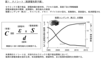
- FIGS 1 and 2 Description of nanosheets (high-dielectric atomic films) Dielectric films are used in electronic components such as multilayer capacitors (MLCCs), capacitors, and memories. In order to achieve miniaturization, high integration, high capacity, and low power consumption in electronic parts, ultra-thin dielectric films are required.
- MLCCs multilayer capacitors
- MLCCs multilayer capacitors
- capacitors capacitors
- memories memories
- the nanosheet of the present invention can design ultra-thin dielectric films, exhibit dielectric properties, insulating properties, and long-term reliability, reduce the size of electronic components, and achieve high performance. can contribute to
- MLCC multilayer capacitors
- the nanosheets (perovskite nanosheets, e.g., ( Ca2Bi )( Ti2Nb2 ) O13, etc. ) constituting the constituent layers of the high-dielectric thin film of the present invention are obtained by subjecting layered perovskite oxides to soft chemical treatment, It is a nanomaterial with two-dimensional anisotropy obtained by exfoliating a single layer, which is the basic minimum unit of the crystal structure.
- the nanosheet of the present invention preferably has a thickness of 10 nm or less (equivalent to several atoms) and a particle size of 100 nm to 1,000 ⁇ m in width.
- the nanosheet (high dielectric atomic film) of the present invention can achieve a higher dielectric constant (1,000 or more) and good insulation properties at the same time even in an ultra-thin film with a thickness of 10 nm or less. It is suitable for application to electronic parts.
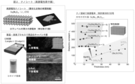
- Figure 3 Description of the nanosheet of the present invention
- the nanosheet of the present invention is obtained by exfoliation from a layered perovskite oxide.
- the perovskite structure is composed of perovskite oxide containing Ti 4+ and Bi 3+ .
- the perovskite oxide is at least one perovskite oxide selected from the group of perovskite oxides represented by the following compositional formulas.
- Composition formula (A 2 Bi)(Ti 2 M 2 )O 13 (where A is a group consisting of divalent metal ions Mg 2+ , Ca 2+ , Sr 2+ , Ba 2+ and Pb 2+ M is at least one pentavalent metal ion selected from the group consisting of pentavalent metal ions Nb 5+ and Ta 5+ ).
- Composition formula: (ABi)( TiM2 ) O10 (where A is at least selected from the group consisting of divalent metal ions Mg2 + , Ca2 + , Sr2 + , Ba2 + , and Pb2 + ) one type of divalent metal ion; M is at least one type of pentavalent metal ion selected from the group consisting of pentavalent metal ions Nb 5+ and Ta 5+ ).
- Compositional formula Bi 2 (Ti 2 M)O 10 (where M is at least one pentavalent metal ion selected from the group consisting of pentavalent metal ions Nb 5+ and Ta 5+ ).
- the perovskite structure is preferably a perovskite structure in which at least three (Ti/M)O 6 octahedra are included in a unit cell.
- the perovskite structure includes four (Ti/M)O 6 octahedra in a unit lattice, and the (A 2 Bi)(Ti 2 M 2 ) As O13 , ( Ca2Bi )( Ti2Nb2 ) O13 , (Sr2Bi) ( Ti2Nb2 ) O13 , ( Ca2Bi )( Ti2Ta2 ) O13 , ( Sr2Bi )( Ti2Ta2 ) O13 , ( Mg2Bi )(Ti2Nb2 ) O13 , ( Ba2Bi )( Ti2Nb2 ) O13 , ( Pb2Bi )( Ti2Nb2 ) O 13 , (Mg2Bi)( Ti2Ta2 ) O13 , (Ba2Bi ) ( Ti2Ta2 ) O13 , ( Pb2Bi )( Ti2Ta2 )( Ti2Ta2 ) O
- the perovskite structure includes four octahedra of (Ti/M)O 6 in a unit cell, and the (ABi 2 )(Ti 3 M)O 13 as ( CaBi2 )( Ti3Nb ) O13 , ( SrBi2 )( Ti3Nb ) O13 , ( CaBi2 )( Ti3Ta ) O13 , ( SrBi2 )( Ti3Ta ) O13 , ( MgBi2 )( Ti3Nb ) O13 , ( BaBi2 )( Ti3Nb ) O13 , ( PbBi2 )( Ti3Nb ) O13 , ( MgBi2 )( Ti3Ta ) O13 , (BaBi 2 ) ( Ti3Nb ) O13 , ( PbBi2 )( Ti3Ta ) O13 , (Ca1 - x
- the perovskite structure includes three octahedra of (Ti/M)O 6 in a unit lattice, and the (ABi)(TiM 2 )O 10 is (CaBi)( TiNb2 ) O10 , (SrBi)( TiNb2 ) O10 , (CaBi)( TiTa2 ) O10 , (SrBi)( TiTa2 ) O10 , (MgBi)( TiNb2 ) O10 , (BaBi)( TiNb2 ) O10 , (PbBi)( TiNb2 ) O10 , (MgBi)( TiTa2 ) O10 , (BaBi)( TiTa2 ) O10 , (PbBi)( TiTa2 ) O10 , (Ca1 - xSrxBi )( TiNb2 ) O10 , (Ca1 - x
- the perovskite structure includes three octahedra of (Ti/M)O 6 in a unit cell, and the Bi 2 (Ti 2 M)O 10 is: ( Bi2 )( Ti2Nb ) O10 , ( Bi2 )( Ti2Ta ) O10 , ( Bi2 )(TiNb2 - xTax ) O10 (0 ⁇ x ⁇ 2), and the like.
- a layered perovskite structure in which at least three octahedra of (Ti/M)O 6 are included in a unit lattice exhibits high dielectric properties and excellent insulating properties. It is possible to artificially reconstruct perovskite oxides containing (Ti/M)O 6 octahedra as basic blocks by extracting them as single nanosheets.
- nanosheet-like perovskite oxides containing (Ti/M)O 6 octahedra can be stably extracted as a single substance, and have a higher dielectric constant than conventional perovskite. It is possible to manufacture and design high dielectric thin films.
- the Ti 4+ ion is largely displaced from the center position of the TiO 6 octahedron depending on the electron configuration of the Ti 4+ ion. Furthermore, the Bi 3+ ion has a lone pair of electrons, which has the effect of enhancing the displacement of the Ti 4+ ion due to its steric hindrance.
- the nanosheets of the present invention are composed of perovskite oxides containing both Ti 4+ and Bi 3+ in the lattice, exhibiting a synergistic effect and exhibiting high dielectric constant and polarization characteristics. Excellent high dielectric and ferroelectric.
- the perovskite oxide forming the perovskite structure preferably has a thickness of 10 nm or less.
- the nanosheet of the present invention it is possible to manufacture and design a nano-level high-dielectric thin film by using, for example, an extremely thin nanosheet-like oxide having a nanosheet thickness of about 1 nm.
- the lateral size of the nanosheet is preferably 10 nm to 1,000 ⁇ m.
- the nanosheet of the present invention preferably has a thickness of 1 nm to 100 nm.
- the nanosheet of the present invention can be used to produce a high-dielectric thin film that functions even with a nanoscale thickness of 100 nm or less, for example, and can exhibit both thinning and high capacity at the same time.
- the nanosheet of the present invention is obtained by exfoliation from a layered perovskite oxide.
- the nanosheets (perovskite nanosheets, e.g., ( Ca2Bi )( Ti2Nb2 ) O13, etc. ) constituting the constituent layers of the high-dielectric thin film of the present invention are obtained by subjecting layered perovskite oxides to soft chemical treatment, It is a nanomaterial with two-dimensional anisotropy obtained by exfoliating a single layer, which is the basic minimum unit of the crystal structure.
- the exfoliation treatment can be called a soft chemical treatment, and this soft chemical treatment is a combination of acid treatment and colloidal treatment.
- a perovskite oxide powder or single crystal having a layered structure is brought into contact with an aqueous acid solution such as hydrochloric acid, and the product is filtered, washed, and dried.
- Alkali metal ions are (all) replaced by hydrogen ions, yielding a hydrogen form material.
- the resulting hydrogen-type substance is put into an aqueous solution of amine or the like and stirred to form a colloid.
- the layers constituting the layered structure are peeled off one by one.
- the thickness of the nanosheets can be controlled in the nanometer range.
- Patent Documents JP-A-2001-270022 and JP-A-2004-255684.
- the peeled nanosheet can be used to form a nanosheet (high dielectric thin film) using the Langmuir-Blodgett method (hereinafter also referred to as the "LB method").
- LB method Langmuir-Blodgett method
- the LB method is a technique known as a method of forming clay minerals or organic nano-thin films, using amphipathic molecules to form an associated film on the air-water interface, which is then transferred to a substrate. It is a technique to fabricate a uniform monolayer film by
- nanosheets by using a low-concentration nanosheet sol solution, the nanosheets are adsorbed on the air-water interface without using amphipathic cationic molecules. By collecting the nanosheets, it is possible to produce a high-quality monolayer film in which the nanosheets are densely and without gaps on the substrate surface.
- nanosheets high dielectric thin films
- the LB method for example, non-patent literature: Kosho Akatsuka, Masa-aki Haga, Yasuo Ebina, Minoru Osada, Katsutoshi Fukuda, Takayoshi Sasaki, "Construction of Highly Ordered Lamellar Nanostructures through Langmuir-Blodgett Deposition of Molecularly Thin Titania Nanosheets of Micrometers of Microsheets Wide and Their Excellent Dielectric Properties", ACS Nano, 3, 1097-1106 (2009), etc.
- nanosheets can be formed by adopting the alternate self-organizing lamination technology proposed in Patent Documents 1 and 2.
- the substrate was (1) immersed in an organic polycation solution, (2) washed with pure water, (3) immersed in a nanosheet sol solution, and (4) washed with pure water.
- the operation is regarded as one cycle, and this is repeated as many times as necessary for at least two types of nanosheets.
- the organic polycation is preferably polyethyleneimine (PEI), polydiallyldimethylammonium chloride (PDDA), polyallylamine hydrochloride (PAH), or the like.
- PEI polyethyleneimine
- PDDA polydiallyldimethylammonium chloride
- PAH polyallylamine hydrochloride
- the present invention is further characterized in that, as a method of forming a single layer of nanosheets, which will be a constituent layer of a high-dielectric thin film, the nanosheets are coated on the surface of the substrate without any gaps, and overlap between the nanosheets is eliminated or reduced.
- a method for forming a monolayer film is provided.
- the means for covering the surface of the substrate with the nanosheet without gaps includes immersing the substrate in a cationic organic polymer solution to cause the substrate surface to adsorb the organic polymer. After that, by immersing the substrate in a colloidal solution in which the flake particles are suspended, the nanosheets are adsorbed on the substrate in a self-organizing manner by electrostatic interaction, which is a process of monolayer formation. formation method.
- the treatment means for removing and reducing overlapping portions between the nanosheets is preferably a method for forming a single layer film by ultrasonic treatment in an alkaline aqueous solution.
- nanosheets high dielectric thin films
- the nanosheet manufacturing method of the present invention is useful for multilayer film manufacturing.
- the organic polymer can be removed by irradiating with ultraviolet rays, and an inorganic nanosheet (high dielectric thin film) can be produced.
- Irradiation with ultraviolet rays is preferably irradiation with ultraviolet rays having a wavelength equal to or shorter than the bandgap, which activates the photocatalytic organic substance decomposition reaction of the layered perovskite oxide, preferably with a xenon light source of 1 mW/cm 2 or more. Irradiate for 12 hours or more.
- the inorganic nanosheet for the formation of the inorganic nanosheet (high-dielectric thin film), preferably, in addition to ultraviolet irradiation, low-temperature heating is also possible, and has the same effect as ultraviolet irradiation.
- the heat treatment is preferably performed at a temperature of 800° C. or less, which is the thermal stability temperature of the layered perovskite oxide, and at a temperature of 300° C. or less for a substrate having a low heat resistance temperature such as a resin substrate such as epoxy.
- the nanosheet of the present invention can be used to fabricate devices by utilizing soft chemical reactions such as self-assembly at room temperature, and problems such as substrate interface deterioration and compositional deviation due to thermal annealing in the conventional manufacturing process can be avoided. It can be avoided and can be fused with various materials.
- the nanosheet of the present invention it is possible to form a film of the nanosheet and mount a capacitor on an epoxy-based resin substrate having a low heat resistance temperature of about 300°C.
- the above method is included as at least a part of the process to manufacture a nanosheet (high dielectric thin film) or an element thereof.
- Nanosheets were fabricated, and as shown in Fig. 4, on an atomic flat epitaxial SrRuO3 substrate, Nanosheets (high-dielectric thin films) with multilayer structures are fabricated by the LB method or alternate self-assembled lamination technology.
- the nanosheet of the present invention By using the nanosheet of the present invention, a low-cost, low-environment process can be realized without the need for large-scale vacuum equipment and expensive film-forming equipment, which are the mainstream of conventional dielectric thin film processes.
- the nanosheet (high dielectric constant nanomaterial) of the present invention can be used in technical fields such as multilayer capacitors, electronic materials such as high frequency devices, IT technology fields, nanoelectronics, etc., where high dielectric constant materials are basic parts. I can.
- High dielectric element with attached nanosheet The present invention includes a high dielectric element with the nanosheet of the present invention attached to an electrode substrate.
- the high dielectric element of the present invention preferably comprises the nanosheet of the present invention between the first electrode substrate and the second electrode substrate.
- the nanosheet of the present invention is attached to at least one of the first and second electrode substrates, and the nanosheet laminate is interposed between the first and second electrode substrates.
- the perovskite oxide preferably constitutes a laminate.
- the method for manufacturing a high dielectric element of the present invention comprises: (1) By the Langmuir-Blodgett method (LB method), a monolayer film is formed on the surface of a substrate by coating the perovskite oxide densely and without gaps, and the monolayer film of the nanosheet of the present invention is formed on the electrode substrate. adhering to (2) A production method for producing the nanosheet laminate of the present invention by repeating the step (1).
- LB method Langmuir-Blodgett method
- the method for manufacturing a high dielectric element of the present invention comprises: (3) immersing the electrode substrate in a cationic organic polymer solution; (4) a step of adsorbing an organic polymer on the surface of the electrode substrate; (5) including a step of immersing the electrode substrate in a colloidal solution in which the nanosheets of the present invention are suspended; (6) A manufacturing method, wherein the nanosheets are adsorbed onto the polymer by electrostatic interaction to produce a laminate of the nanosheets.
- ultrasonic waves are applied to remove overlapping portions of the nanosheets. Remove.
- ultraviolet rays are applied to remove the organic polymer.
- the organic polymer is removed by heating.
- a high dielectric element of the present invention it is possible to manufacture an inorganic high dielectric element from which organic matter has been removed, and problems such as deterioration of the substrate interface and composition deviation can be avoided compared to the heat treatment process of the conventional element manufacturing process. It is possible to eliminate the problem and manufacture a high-performance high-dielectric device.
- a high dielectric element of the present invention it is possible to stably and easily manufacture an inorganic high dielectric element from which organic substances are removed by low-temperature heating. It is possible to solve problems such as substrate interface deterioration and composition deviation, and to provide a high-performance high-dielectric element.
- the handling of the nanosheet of the present invention becomes easy, and the element using the nanosheet productivity can be ensured.
- the capacitor structure element using the nanosheet of the present invention can ensure the productivity and stability of high dielectric elements.
- the high-dielectric element manufacturing method of the present invention can manufacture a high-quality high-dielectric thin film in which the nanosheet of the present invention is densely and without gaps coated on the substrate surface.
- the high-dielectric element manufacturing method of the present invention does not require annealing at a high temperature, etc., compared to the conventional high-dielectric thin film process, and the solution process at room temperature is possible.
- a high-performance high-dielectric device can be manufactured by avoiding problems such as interface deterioration and composition deviation.
- the low-cost room-temperature solution process uses a beaker and tweezers, which requires a large-sized vacuum apparatus and an expensive process compared to the conventional high-dielectric thin film process.
- a low-cost and low-environment process can be realized without requiring a film forming apparatus.
- Figure 4 Description of a high dielectric device to which the nanosheets of the present invention are attached
- Figure 4 shows one embodiment of a high dielectric device to which the nanosheets of the present invention are attached.
- 1 is a diagram schematically illustrating a cross-sectional structure of a high dielectric material composed of
- (1) is a lower electrode substrate (hereinafter also referred to as “substrate (1)”) made of atomically flat epitaxial SrRuO3
- (2) is the present substrate formed on the substrate (1).
- the high-dielectric thin film structure (3) comprising a high-dielectric nanosheet (nanosheet-like perovskite oxide, hereinafter also referred to as “perovskite nanosheet”) of the invention is an upper electrode made of gold.
- FIG. 4 shows an example in which a multilayer structure is formed by laminating perovskite nanosheets (2) on a lower electrode substrate (1) made of SrRuO3 .
- the lower electrode substrate (1) is not limited to, for example, an atomically flat epitaxial substrate, and other metal electrodes such as gold, platinum, copper, aluminum; conductive substrates such as Nb-doped SrTiO3 ; A perovskite nanosheet thin film may also be disposed on a perovskite substrate; a transparent oxide electrode such as ITO, Ga-doped ZnO, Nb-doped TiO2 ; a substrate such as Si, glass, plastic, or the like.
- the upper electrode (3) may be of various types like the lower electrode substrate (1).
- the nanosheet of the present invention is composed of the highly dielectric nanosheet of the present invention or a laminate of such nanosheets.
- the nanosheet thin film is adhered to the upper electrode substrate (3), and both are laminated together.
- the nanosheet of the present invention By applying the nanosheet of the present invention to capacitors, etc., it is possible to obtain elements with a higher capacity than conventional dielectric oxide materials. Further, the nanosheet of the present invention can be arbitrarily designed in various forms for suppression of leakage current, reduction of current consumption, and high integration of capacitors.
- nanosheet of the present invention By applying the nanosheet of the present invention to high-dielectric thin films and high-dielectric devices by forming multilayer structures on, for example, atomically flat epitaxial SrRuO3 substrates and Pt, thin film capacitors, multilayer capacitors, It can be used for high frequency devices, DRAM memories, gate insulators for transistors, etc.
- the nanosheet of the present invention can simultaneously achieve a high dielectric constant and good insulating properties even in the nano region by utilizing the nanophysical properties and high organization and structure controllability of perovskite nanosheets.
- Example 1 In Example 1, layered perovskite oxide K( Ca2Bi )( Ti2Nb2 ) O13 was used as a starting material to synthesize perovskite nanosheets ( Ca2Bi )( Ti2Nb2 ) O13 , which consisted of nanosheets . A dielectric device was manufactured.
- Non-Patent Document 1 Kosho Akatsuka, Masa-aki Haga, Yasuo Ebina, Minoru Osada, Katsutoshi Fukuda, Takayoshi Sasaki, “Construction of Highly Ordered Lamellar Nanostructures through Langmuir-Blodgett Deposition of Molecularly Thin Titania Nanosheets Tens of Micrometers Wide and Their Excellent Dielectric Properties”, ACS Nano, 3, 1097-1106 (2009)).
- a dense monolayer film consisting of nanosheets was formed at the gas-liquid interface by the LB method.
- a single-layer film in which the nanosheets covered the substrate surface like tiles without gaps was fabricated.
- a 5-layer multilayer film or a 10-layer multilayer film consisting of (Ca 2 Bi)(Ti 2 Nb 2 )O 10 nanosheets was fabricated by repeating the preparation of a single layer film and the transfer operation.
- the resulting nanosheet multilayer film was irradiated with ultraviolet light (wavelength: 200 to 300 nm, intensity: 1 mW/cm 2 ) for 72 hours to remove organic substances present between the nanosheet monolayer films.
- a probe was applied to each of the upper electrode (Au) and the lower electrode (SrRuO 3 ) to evaluate the insulating properties and dielectric properties.
- the leakage current density at +1 V applied voltage was evaluated using a semiconductor parameter analyzer (4200-SCS) manufactured by Keithley.
- a high-precision impedance analyzer (4294A) manufactured by Agilent Technologies was used to measure the capacitance at a frequency of 10 kHz and calculate the relative permittivity.
- Table 1 summarizes the leakage current density and dielectric constant.
- the insulating properties (leakage current properties) of the nanosheet thin films showed good insulating properties of 10 -7 A/cm 2 or less in all ultra-thin films of 10 nm to 20 nm.
- the dielectric properties (relative permittivity) of the nanosheet thin film showed a high relative permittivity of 1,140 or more, regardless of the number of layers.
- the nanosheet of the present invention can be evaluated as a high dielectric thin film that simultaneously achieves stable high dielectric properties and insulating properties in a thin film with a nanoscale film thickness (20 nm or less).
- Example 2 in order to investigate the composition dependence of dielectric properties, nanosheets with different chemical compositions were synthesized, dielectric elements consisting of microelectrodes on a single layer film were produced, and the properties were evaluated.
- Example 2 The same LB method as in Example 1 was used to form the nanosheets.
- the single layer film is irradiated with ultraviolet light (wavelength: 200-300 nm, intensity: 1 mW/cm 2 ) for 72 hours to remove organic matter between the nanosheet single layer film and the substrate. bottom.
- ultraviolet light wavelength: 200-300 nm, intensity: 1 mW/cm 2
- Table 2 summarizes the leakage current density and dielectric constant.
- the leakage current characteristics of the nanosheet thin films all exhibited good insulation characteristics of 10 ⁇ 7 A/cm 2 or less regardless of the chemical composition.
- the dielectric constant of the nanosheet thin film showed a high dielectric constant of 940 or more.
- Nanosheet thin films are also applicable to (SrBi 2 )(Ti 3 Nb)O 13 , (SrBi 2 )(Ti 3 Ta)O 13 and the like (FIG. 5).
- the nanosheet of the present invention can be evaluated as having high dielectric properties, which is a feature common to nanosheets containing Ti and Bi.
- the nanosheet (high dielectric atomic film) of the present invention is a useful material that not only exhibits a high dielectric constant, but also achieves high withstand voltage (>4 MV/cm) and high heat resistance (>800°C) at the same time. be.
- the nanosheet of the present invention is a useful material that exhibits high stability even after accelerated tests at high temperatures (100° C., 1,000 hours), similar to multilayer capacitors.
- the nanosheet of the present invention makes it possible to manufacture high-performance capacitors, memories, capacitors, etc. that achieve both miniaturization and large capacity at the same time.
- INDUSTRIAL APPLICABILITY The nanosheet of the present invention is useful for practical applications such as large-area film formation, lamination, and device production using high-dielectric atomic films.
- the nanosheet of the present invention is an atomic film composed of a perovskite structure oxide (( Ca2Bi )( Ti2Nb2 ) O13 etc.) containing Ti4 + and Bi3 + among compounds having a layered perovskite structure. and exhibits a high dielectric constant of 1,000 or more.
- a perovskite structure oxide (( Ca2Bi )( Ti2Nb2 ) O13 etc.) containing Ti4 + and Bi3 + among compounds having a layered perovskite structure. and exhibits a high dielectric constant of 1,000 or more.
- the nanosheets of the present invention can function as thin films and simultaneously achieve a high dielectric constant and good insulating properties.
- the nanosheet of the present invention has a thickness of 10 nm or less, and can simultaneously achieve ⁇ r >800, leakage current ⁇ 10 ⁇ 7 A/cm 2 at 1 V, high permittivity, and insulating function.
- the nanosheet of the present invention can achieve, for example, 1/100 reduction in size and 1,000 times or more increase in capacity at the same time as compared with conventional high-dielectric films (barium titanate (BaTiO 3 )-based thin films).
- conventional high-dielectric films barium titanate (BaTiO 3 )-based thin films.
- the nanosheet of the present invention is (1) It functions with the smallest thin film among conventional materials, and simultaneously achieves a high dielectric constant and good insulation properties. (2) element manufacturing by room-temperature, low-cost solution process; (3) By realizing a room temperature process, problems associated with conventional thermal annealing can be solved. (4) It is possible to form a high-dielectric thin film on a resin substrate, etc., and to mount a capacitor. (5) It does not require large-scale vacuum equipment, expensive film-forming equipment, etc., which are the mainstream of conventional dielectric thin film processes, and has the advantage of realizing a low-cost and low-environment process.
- the nanosheet of the present invention can be used in all kinds of electronic devices such as multilayer capacitors, high frequency devices, DRAM memories, and gate insulators for transistors.
- the nanosheet of the present invention can be used to manufacture elements by room-temperature and low-cost solution processes. It is possible.
Landscapes
- Chemical & Material Sciences (AREA)
- Organic Chemistry (AREA)
- Engineering & Computer Science (AREA)
- Inorganic Chemistry (AREA)
- Nanotechnology (AREA)
- Physics & Mathematics (AREA)
- Composite Materials (AREA)
- Condensed Matter Physics & Semiconductors (AREA)
- General Physics & Mathematics (AREA)
- Materials Engineering (AREA)
- Crystallography & Structural Chemistry (AREA)
- Inorganic Insulating Materials (AREA)
Priority Applications (1)
| Application Number | Priority Date | Filing Date | Title |
|---|---|---|---|
| JP2023552932A JPWO2023058703A1 (https=) | 2021-10-08 | 2022-10-06 |
Applications Claiming Priority (2)
| Application Number | Priority Date | Filing Date | Title |
|---|---|---|---|
| JP2021166184 | 2021-10-08 | ||
| JP2021-166184 | 2021-10-08 |
Publications (1)
| Publication Number | Publication Date |
|---|---|
| WO2023058703A1 true WO2023058703A1 (ja) | 2023-04-13 |
Family
ID=85804338
Family Applications (1)
| Application Number | Title | Priority Date | Filing Date |
|---|---|---|---|
| PCT/JP2022/037372 Ceased WO2023058703A1 (ja) | 2021-10-08 | 2022-10-06 | 高誘電性原子膜 |
Country Status (2)
| Country | Link |
|---|---|
| JP (1) | JPWO2023058703A1 (https=) |
| WO (1) | WO2023058703A1 (https=) |
Citations (3)
| Publication number | Priority date | Publication date | Assignee | Title |
|---|---|---|---|---|
| WO2006013826A1 (ja) * | 2004-08-06 | 2006-02-09 | Japan Science And Technology Agency | Bi層状化合物ナノプレート及びその配列体並びにそれらの製造方法とそれを用いた装置 |
| JP2014152052A (ja) * | 2013-02-06 | 2014-08-25 | National Institute For Materials Science | ホモロガス系列層状ペロブスカイト酸化物に基づくペロブスカイトナノシート、および、その用途 |
| US20200266264A1 (en) * | 2019-02-14 | 2020-08-20 | Samsung Electronics Co., Ltd. | Single crystal material and method of forming the same and stacked structure and ceramic electronic component and device |
-
2022
- 2022-10-06 JP JP2023552932A patent/JPWO2023058703A1/ja active Pending
- 2022-10-06 WO PCT/JP2022/037372 patent/WO2023058703A1/ja not_active Ceased
Patent Citations (3)
| Publication number | Priority date | Publication date | Assignee | Title |
|---|---|---|---|---|
| WO2006013826A1 (ja) * | 2004-08-06 | 2006-02-09 | Japan Science And Technology Agency | Bi層状化合物ナノプレート及びその配列体並びにそれらの製造方法とそれを用いた装置 |
| JP2014152052A (ja) * | 2013-02-06 | 2014-08-25 | National Institute For Materials Science | ホモロガス系列層状ペロブスカイト酸化物に基づくペロブスカイトナノシート、および、その用途 |
| US20200266264A1 (en) * | 2019-02-14 | 2020-08-20 | Samsung Electronics Co., Ltd. | Single crystal material and method of forming the same and stacked structure and ceramic electronic component and device |
Non-Patent Citations (4)
| Title |
|---|
| MATSUDA H, ET AL.: "SYNTHESIS AND ELECTRICAL PROPERTIES OF SR- AND NB-COSUBSTITUTED BI4-XSRXTI3-XNBXO12 POLYCRYSTALLINE THIN FILMS", JAPANESE JOURNAL OF APPLIED PHYSICS, JAPAN SOCIETY OF APPLIED PHYSICS, JP, vol. 42, no. 08A, PART 02, 1 August 2003 (2003-08-01), JP , pages L949 - L952, XP001190780, ISSN: 0021-4922, DOI: 10.1143/JJAP.42.L949 * |
| NAKAZAKI, KOTA; SAKURABA, TOSHINORI; YAMAMOTO, EISUKE; KOBAYASHI, MAKOTO; OSADA, MINORU: "A08-2am-13 Synthesis and exfoliation of Dion-Jacobson type perovskite ferroelectric RbBi2Ti2NbO10", PROCEEDINGS OF THE 101ST ANNUAL MEETING OF THE CHEMICAL SOCIETY OF JAPAN (CSJ); [ONLINE]; MARCH 19-22, 2021, vol. 101, 4 March 2021 (2021-03-04) - 22 March 2021 (2021-03-22), pages A08 - 2am, XP009546266 * |
| SHAO LUHUA; LI SIJIAN; YANG WENWU; YANG ZHENFEI; XIA XINNIAN; LIU YUTANG: "Crystallinity-dependent photodegradation of metallic Bi in situ grown on perovskite Bi3TiNbO9 nanosheets toward antibiotic", CHEMOSPHERE, PERGAMON PRESS, OXFORD., GB, vol. 285, 12 July 2021 (2021-07-12), GB , XP086837695, ISSN: 0045-6535, DOI: 10.1016/j.chemosphere.2021.131554 * |
| YANG P, ET AL.: "OPTICAL LIMITING IN SRBI2TA2O9 AND PBZRXTI1-XO3 FERROELETRIC THIN FILMS", APPLIED PHYSICS LETTERS, AMERICAN INSTITUTE OF PHYSICS, 2 HUNTINGTON QUADRANGLE, MELVILLE, NY 11747, vol. 80, no. 18, 6 May 2002 (2002-05-06), 2 Huntington Quadrangle, Melville, NY 11747, pages 3394 - 3396, XP001123339, ISSN: 0003-6951, DOI: 10.1063/1.1477618 * |
Also Published As
| Publication number | Publication date |
|---|---|
| JPWO2023058703A1 (https=) | 2023-04-13 |
Similar Documents
| Publication | Publication Date | Title |
|---|---|---|
| JP5885150B2 (ja) | 高誘電性ナノシート積層体、高誘電性ナノシート積層体、高誘電体素子、および高誘電体薄膜素子の製造方法 | |
| JP5610348B2 (ja) | 誘電体膜と誘電体素子及びその製造方法 | |
| JP5688816B2 (ja) | 超格子構造を有する強誘電体薄膜とその製造方法、並びに強誘電体素子とその製造方法 | |
| JP5294201B2 (ja) | 誘電体素子とその製造方法 | |
| Osada et al. | High-κ dielectric nanofilms fabricated from titania nanosheets | |
| Osada et al. | Two‐dimensional dielectric nanosheets: novel nanoelectronics from nanocrystal building blocks | |
| Li et al. | Engineered interfaces of artificial perovskite oxide superlattices via nanosheet deposition process | |
| Osada et al. | Robust high-κ response in molecularly thin perovskite nanosheets | |
| Li et al. | High thermal robustness of molecularly thin perovskite nanosheets and implications for superior dielectric properties | |
| Khan et al. | Scalable Design of Two‐Dimensional Oxide Nanosheets for Construction of Ultrathin Multilayer Nanocapacitor | |
| KR102469185B1 (ko) | 세라믹 전자 부품 및 그 제조 방법과 전자장치 | |
| Ma et al. | Organization of artificial superlattices utilizing nanosheets as a building block and exploration of their advanced functions | |
| CN110246689A (zh) | 陶瓷电解质及其制造方法和陶瓷电子组件及电子设备 | |
| JPWO2007094244A1 (ja) | ナノ超薄膜誘電体とその製造方法及びナノ超薄膜誘電体素子 | |
| Yoo et al. | Layer control of Sr1. 8Bi0. 2Nan-3NbnO3n+ 1 (n= 3–5) perovskite nanosheets: dielectric to ferroelectric transition of film deposited by Langmuir Blodgett method | |
| WO2023058703A1 (ja) | 高誘電性原子膜 | |
| Li et al. | Solution-based fabrication of perovskite multilayers and superlattices using nanosheet process | |
| Osada et al. | New dielectric nanomaterials fabricated from nanosheet technique | |
| Osada et al. | Solution-based fabrication of high-κ dielectric nanofilms using titania nanosheets as a building block | |
| Osada | Emerging ceramic nanosheets: From tailored synthesis to electronic applications | |
| Osada et al. | Solution-based fabrication of high-k dielectrics using oxide nanosheets | |
| JP2022088333A (ja) | ニオベート誘電体を含むナノシートおよびこれを含む誘電体薄膜 | |
| Osada et al. | Room-temperature fabrication for functional oxide nanofilms using oxide nanosheets | |
| Osada et al. | Room-temperature ceramic nanocoating using nanosheet deposition technique |
Legal Events
| Date | Code | Title | Description |
|---|---|---|---|
| 121 | Ep: the epo has been informed by wipo that ep was designated in this application |
Ref document number: 22878571 Country of ref document: EP Kind code of ref document: A1 |
|
| WWE | Wipo information: entry into national phase |
Ref document number: 2023552932 Country of ref document: JP |
|
| NENP | Non-entry into the national phase |
Ref country code: DE |
|
| 122 | Ep: pct application non-entry in european phase |
Ref document number: 22878571 Country of ref document: EP Kind code of ref document: A1 |