WO2023058399A1 - 電波反射装置 - Google Patents
電波反射装置 Download PDFInfo
- Publication number
- WO2023058399A1 WO2023058399A1 PCT/JP2022/033715 JP2022033715W WO2023058399A1 WO 2023058399 A1 WO2023058399 A1 WO 2023058399A1 JP 2022033715 W JP2022033715 W JP 2022033715W WO 2023058399 A1 WO2023058399 A1 WO 2023058399A1
- Authority
- WO
- WIPO (PCT)
- Prior art keywords
- radio wave
- patch electrode
- layer
- dielectric
- dielectric substrate
- Prior art date
- Legal status (The legal status is an assumption and is not a legal conclusion. Google has not performed a legal analysis and makes no representation as to the accuracy of the status listed.)
- Ceased
Links
Images





Classifications
-
- G—PHYSICS
- G02—OPTICS
- G02F—OPTICAL DEVICES OR ARRANGEMENTS FOR THE CONTROL OF LIGHT BY MODIFICATION OF THE OPTICAL PROPERTIES OF THE MEDIA OF THE ELEMENTS INVOLVED THEREIN; NON-LINEAR OPTICS; FREQUENCY-CHANGING OF LIGHT; OPTICAL LOGIC ELEMENTS; OPTICAL ANALOGUE/DIGITAL CONVERTERS
- G02F1/00—Devices or arrangements for the control of the intensity, colour, phase, polarisation or direction of light arriving from an independent light source, e.g. switching, gating or modulating; Non-linear optics
- G02F1/01—Devices or arrangements for the control of the intensity, colour, phase, polarisation or direction of light arriving from an independent light source, e.g. switching, gating or modulating; Non-linear optics for the control of the intensity, phase, polarisation or colour
- G02F1/13—Devices or arrangements for the control of the intensity, colour, phase, polarisation or direction of light arriving from an independent light source, e.g. switching, gating or modulating; Non-linear optics for the control of the intensity, phase, polarisation or colour based on liquid crystals, e.g. single liquid crystal display cells
- G02F1/133—Constructional arrangements; Operation of liquid crystal cells; Circuit arrangements
- G02F1/1333—Constructional arrangements; Manufacturing methods
- G02F1/1343—Electrodes
- G02F1/134309—Electrodes characterised by their geometrical arrangement
- G02F1/134336—Matrix
-
- G—PHYSICS
- G02—OPTICS
- G02F—OPTICAL DEVICES OR ARRANGEMENTS FOR THE CONTROL OF LIGHT BY MODIFICATION OF THE OPTICAL PROPERTIES OF THE MEDIA OF THE ELEMENTS INVOLVED THEREIN; NON-LINEAR OPTICS; FREQUENCY-CHANGING OF LIGHT; OPTICAL LOGIC ELEMENTS; OPTICAL ANALOGUE/DIGITAL CONVERTERS
- G02F1/00—Devices or arrangements for the control of the intensity, colour, phase, polarisation or direction of light arriving from an independent light source, e.g. switching, gating or modulating; Non-linear optics
- G02F1/01—Devices or arrangements for the control of the intensity, colour, phase, polarisation or direction of light arriving from an independent light source, e.g. switching, gating or modulating; Non-linear optics for the control of the intensity, phase, polarisation or colour
- G02F1/13—Devices or arrangements for the control of the intensity, colour, phase, polarisation or direction of light arriving from an independent light source, e.g. switching, gating or modulating; Non-linear optics for the control of the intensity, phase, polarisation or colour based on liquid crystals, e.g. single liquid crystal display cells
- G02F1/133—Constructional arrangements; Operation of liquid crystal cells; Circuit arrangements
- G02F1/1333—Constructional arrangements; Manufacturing methods
- G02F1/133302—Rigid substrates, e.g. inorganic substrates
-
- H—ELECTRICITY
- H01—ELECTRIC ELEMENTS
- H01Q—ANTENNAS, i.e. RADIO AERIALS
- H01Q15/00—Devices for reflection, refraction, diffraction or polarisation of waves radiated from an antenna, e.g. quasi-optical devices
- H01Q15/14—Reflecting surfaces; Equivalent structures
-
- H—ELECTRICITY
- H01—ELECTRIC ELEMENTS
- H01Q—ANTENNAS, i.e. RADIO AERIALS
- H01Q15/00—Devices for reflection, refraction, diffraction or polarisation of waves radiated from an antenna, e.g. quasi-optical devices
- H01Q15/14—Reflecting surfaces; Equivalent structures
- H01Q15/148—Reflecting surfaces; Equivalent structures with means for varying the reflecting properties
-
- H—ELECTRICITY
- H01—ELECTRIC ELEMENTS
- H01Q—ANTENNAS, i.e. RADIO AERIALS
- H01Q3/00—Arrangements for changing or varying the orientation or the shape of the directional pattern of the waves radiated from an antenna or antenna system
- H01Q3/44—Arrangements for changing or varying the orientation or the shape of the directional pattern of the waves radiated from an antenna or antenna system varying the electric or magnetic characteristics of reflecting, refracting, or diffracting devices associated with the radiating element
Definitions
- An embodiment of the present invention relates to a radio wave reflector capable of controlling the traveling direction of reflected radio waves.
- a phased array antenna device controls the directivity of a fixed antenna by adjusting the amplitude and phase of the high-frequency signal applied to each of the multiple antenna elements arranged in a plane. ing.
- a phased array antenna system requires a phase shifter.
- a phased array antenna device using a phase shifter that utilizes a change in dielectric constant depending on the alignment state of liquid crystal has been disclosed (see, for example, Patent Document 1).
- 5G fifth-generation communication standard
- This communication standard adopts frequencies in the millimeter wave band from 26 GHz to 28 GHz.
- Communication according to the 5G standard can achieve very high throughput by adopting frequencies in the millimeter wave band, enabling transmission over a wide bandwidth.
- radio waves with frequencies in the millimeter wave band have a characteristic of being highly straight and difficult to propagate around obstacles. As a result, there is a problem that the communication area that can be covered by the 5G standard is becoming narrower in urban areas.
- one of the objects of one embodiment of the present invention is to provide a radio wave reflector with high reflection gain.
- a radio wave reflector comprises at least one patch electrode, a ground conductor layer facing the at least one patch electrode and spaced apart from the at least one patch electrode, and at least one a liquid crystal layer between the patch electrode and the ground conductor layer; and a dielectric substrate provided on a surface of the at least one patch electrode opposite to the liquid crystal layer, the liquid crystal layer side of the at least one patch electrode.
- the thickness T from the surface of the dielectric substrate to the surface of the dielectric substrate opposite to the at least one patch electrode has a thickness corresponding to a quarter wavelength of the wavelength of the radio wave irradiated to the at least one patch electrode .
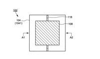
- FIG. 4 shows a plan view of a reflector unit cell used in the radio wave reflector according to one embodiment of the present invention
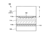
- 1B is a plan view of the reflector unit cell used in the radio wave reflector according to one embodiment of the present invention, showing the cross-sectional structure between A1 and A2 shown in FIG. 1A.
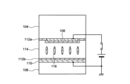
- FIG. 4 shows a state in which no voltage is applied between the patch electrode and the ground electrode in the reflector unit cell used in the radio wave reflector according to the embodiment of the present invention
- 4 shows a state in which a voltage is applied between the patch electrode and the ground electrode in the reflector unit cell used in the radio wave reflector according to the embodiment of the present invention
- FIG. 4 shows a plan view of a reflector unit cell used in the radio wave reflector according to one embodiment of the present invention
- 1B is a plan view of the reflector unit cell used in the radio wave reflector according to one embodiment of the present invention, showing the cross-sectional structure between A1 and A2 shown in FIG. 1A.
- 1 shows a cross-sectional structure of a reflector unit cell used in a radio wave reflector according to an embodiment of the present invention
- 1 shows a cross-sectional structure of a reflector unit cell used in a radio wave reflector according to an embodiment of the present invention
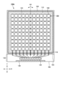
- 1 shows the configuration of a radio wave reflecting device according to an embodiment of the present invention
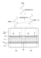
- 4 schematically shows that the traveling direction of reflected waves is changed by the radio wave reflecting device according to one embodiment of the present invention.
- 1 shows the configuration of a radio wave reflecting device according to an embodiment of the present invention
- 4 shows a cross-sectional structure of a reflector unit cell in a radio wave reflector according to an embodiment of the present invention
- a member or region when a member or region is “above (or below)” another member or region, it means directly above (or directly below) the other member or region unless otherwise specified. Includes not only one case but also the case above (or below) another member or region, that is, the case where another component is included between above (or below) another member or region .
- FIGS. 1A and 1B show a reflector unit cell 102 used in a radio wave reflector according to an embodiment of the present invention.
- FIG. 1A shows a plan view when the reflector unit cell 102 is viewed from above (the side on which radio waves are incident), and
- FIG. 1B shows a cross-sectional view between A1-A2 shown in the plan view.
- the reflector unit cell 102 includes a dielectric substrate 104, a counter substrate 106, a patch electrode 108, a ground electrode 110, a liquid crystal layer 114, a first alignment film 112a and a second alignment film 112b.
- the dielectric substrate 104 forming one layer in the reflector unit cell 102 can also be regarded as a dielectric layer.
- the patch electrode 108 is provided on the dielectric substrate (dielectric layer) 104 and the ground electrode 110 is provided on the opposing substrate 106 .
- a first alignment film 112 a is provided on the dielectric substrate (dielectric layer) 104 to cover the patch electrode 108
- a second alignment film 112 b is provided on the opposing substrate 106 to cover the ground electrode 110 .
- the patch electrode 108 and the ground electrode 110 are arranged to face each other, and a liquid crystal layer 114 is provided between them.
- a first alignment film 112 a is interposed between the patch electrode 108 and the liquid crystal layer 114
- a second alignment film 112 b is interposed between the ground electrode 110 and the liquid crystal layer 114 .
- the patch electrode 108 preferably has a shape that is symmetrical with respect to the vertically polarized wave and the horizontally polarized wave of the incident radio wave, and has a square or circular shape in plan view.
- FIG. 1A shows a case where the patch electrode 108 is square in plan view.
- the shape of the ground electrode 110 is not particularly limited, and has a shape that extends over substantially the entire surface of the counter substrate 106 so as to have a wider area than the patch electrode 108 .
- Materials for forming the patch electrode 108 and the ground electrode 110 are not limited, and they are formed using a conductive metal or metal oxide.
- a first wiring 118 may be provided on the dielectric substrate (dielectric layer) 104 .
- a first wiring 118 is connected to the patch electrode 108 .
- the first wiring 118 can be used when applying a control signal to the patch electrode 108 .
- the first wiring 118 can be used to connect a given patch electrode to its adjacent patch electrode.
- the dielectric substrate (dielectric layer) 104 and the opposing substrate 106 are bonded together with a sealing material.
- a dielectric substrate (dielectric layer) 104 and a counter substrate 106 are arranged to face each other with a gap therebetween, and a liquid crystal layer 114 is provided in a region surrounded by a sealing material.
- the liquid crystal layer 114 is provided so as to fill the gap between the dielectric substrate (dielectric layer) 104 and the opposing substrate 106 .
- the distance between the dielectric substrate (dielectric layer) 104 and the counter substrate 106 is 20 to 100 ⁇ m, for example, 50 ⁇ m.
- the patch electrode 108, the ground electrode 110, the first alignment film 112a, and the second alignment film 112b are provided between the dielectric substrate (dielectric layer) 104 and the counter substrate 106, the dielectric substrate 104 and the first alignment film 112 a and the second alignment film 112 b provided on each of the counter substrates 106 becomes the thickness of the liquid crystal layer 114 .
- a spacer may be provided between the dielectric substrate (dielectric layer) 104 and the opposing substrate 106 to keep the distance constant.
- a control signal for controlling the orientation of liquid crystal molecules in the liquid crystal layer 114 is applied to the patch electrode 108 .
- the control signal is a DC voltage signal or a polarity reversal signal in which a positive DC voltage and a negative DC voltage are alternately inverted.
- the ground electrode 110 is applied with an intermediate level voltage of ground or a polarity inversion signal.
- a liquid crystal material having dielectric anisotropy is used for the liquid crystal layer 114 .
- nematic liquid crystal, smectic liquid crystal, cholesteric liquid crystal, or discotic liquid crystal can be used as the liquid crystal layer 114 .
- the liquid crystal layer 114 having dielectric anisotropy changes its dielectric constant according to the change in the alignment state of the liquid crystal molecules.
- the reflector unit cell 102 can change the dielectric constant of the liquid crystal layer 114 by a control signal applied to the patch electrode 108, thereby delaying the phase of the reflected wave when reflecting the radio wave.
- the frequency bands of radio waves reflected by the reflector unit cell 102 include a very high frequency (VHF) band, an ultra-high frequency (UHF) band, a microwave (SHF: super high frequency) band, and a submillimeter wave ( THF: Tremendously high frequency) and millimeter wave (EHF: Extra High Frequency) band.
- VHF very high frequency
- UHF ultra-high frequency
- SHF microwave
- THF Tremendously high frequency
- EHF Extra High Frequency
- FIG. 2A shows a state in which no voltage is applied between the patch electrode 108 and the ground electrode 110 (referred to as "first state”).
- FIG. 2A shows a case where the first alignment layer 112a and the second alignment layer 112b are horizontal alignment layers. The long axes of the liquid crystal molecules 116 in the first state are aligned horizontally with respect to the surfaces of the patch electrode 108 and the ground electrode 110 by the first alignment film 112a and the second alignment film 112b.
- FIG. 2B shows a state in which a control signal (voltage signal) is applied to the patch electrode 108 (referred to as "second state").
- the liquid crystal molecules 116 are oriented with their long axes perpendicular to the surfaces of the patch electrode 108 and the ground electrode 110 under the action of the electric field.
- the angle at which the long axes of the liquid crystal molecules 116 are oriented is oriented in an intermediate direction between the horizontal direction and the vertical direction depending on the magnitude of the control signal applied to the patch electrode 108 (the magnitude of the voltage between the counter electrode and the patch electrode).
- the second state has a larger dielectric constant than the first state.
- the apparent dielectric constant is smaller in the second state than in the first state.
- the liquid crystal layer 114 with dielectric anisotropy can also be regarded as a variable dielectric layer.
- the reflector unit cell 102 can be controlled to delay (or not delay) the phase of the reflected wave using the dielectric anisotropy of the liquid crystal layer 114 .
- the reflector unit cell 102 is used as a reflector that reflects radio waves in a predetermined direction. Preferably, the reflector unit cell 102 does not attenuate the amplitude of the reflected radio wave as much as possible.
- the dielectric substrate (dielectric layer) 104 is made of a dielectric material such as glass or resin. Since the radio wave changes its phase velocity when passing through the dielectric, it is necessary to consider the thickness of the dielectric substrate (dielectric layer) 104 in order not to attenuate the amplitude of the reflected wave.
- FIG. 3 shows the result of simulating the relationship between the thickness of the dielectric substrate (dielectric layer) 104 (that is, the thickness of the dielectric layer) and the amplitude of the reflected wave.
- the simulation shown in FIG. 3 is a state in which a plurality of reflector unit cells 102 are arranged, and assumes a reflector of a radio wave reflector.
- the size of the patch electrodes 108 in the reflector unit cell 102 is 2.85 mm ⁇ 2.85 mm, and the condition is set that the patch electrodes 108 of this size are arranged at a pitch of 3.5 mm.
- the thickness of the liquid crystal layer 114 of the reflector unit cell 102 is set to 50 ⁇ m, and the thickness of the dielectric substrate (dielectric layer) 104 is used as a parameter for calculation.
- the frequency of radio waves is 28 GHz. This simulation was performed using GST Studio Suite (manufactured by Dassault Systèmes, Inc.).
- FIG. 3 is a graph showing the result of simulating the relationship between the thickness of the dielectric substrate (dielectric layer) 104 and the amplitude of the reflected wave.
- Table 1 also shows numerical data obtained in the same simulation. From the graph shown in FIG. 3 and Table 1, it can be seen that the amplitude of the reflected wave changes depending on the thickness of the dielectric substrate (dielectric layer) 104 . Specifically, when the thickness of the dielectric substrate (dielectric layer) 104 is 1.1 mm, the amplitude of the reflected wave is ⁇ 4.3 dB, which is the maximum within the range of this simulation.
- the amplitude of the reflected wave is approximately within the range of -2 dB, which is within a favorable range. has been confirmed.
- the thickness T can be the length from the surface of the patch electrode 108 on the liquid crystal layer 114 side to the surface of the dielectric substrate (dielectric layer) 104 opposite to the surface on which the patch electrode 108 is provided.
- the thickness T of the dielectric substrate (dielectric layer) 104 shown in Equation (1) is the effective thickness for radio waves incident on the reflector unit cell 102 .
- the dielectric substrate (dielectric layer) 104 need not be a single body (or single layer), and may be formed from multiple dielectric substrates or multiple dielectric layers.
- FIG. 4A shows an example in which the dielectric substrate (dielectric layer) 104 is formed of a plurality of substrates (first substrate 105a, second substrate 105b).
- the first substrate 105a and the second substrate 105b may be glass substrates made of the same or different glass material, or one may be a glass substrate and the other a resin film substrate.
- the number of dielectric substrates (dielectric layers) 104 to be laminated is not limited, and the number of substrates is not limited as long as the relationship shown in formula (1) is satisfied.
- FIG. 4B shows an example in which the dielectric substrate (dielectric layer) 104 includes multiple types of dielectric materials. Specifically, an example in which the dielectric substrate (dielectric layer) 104 is formed of a first glass substrate 1041, a first resin film 1042a and a second resin film 1042b is shown. In the example shown in FIG. 4B as well, the number of resin films to be laminated on the first glass substrate 1041 is not limited, and the number of resin films to be laminated is not limited as long as the thickness T shown in formula (1) is satisfied. By laminating a plurality of resin films in this manner, the thickness T can be adjusted according to the wavelength of the radio wave reflected by the patch electrode 108 .
- the dielectric substrate (dielectric layer) 104 located on the upper surface of the patch electrode 108 has a thickness corresponding to a quarter wavelength of the wavelength of the reflected radio wave, thereby reducing the amplitude of the reflected wave. can be enhanced.
- the dielectric substrate (dielectric layer) 104 is not limited to a single substrate (or a single layer), and may be in a state in which multiple dielectrics are stacked, so the thickness of the dielectric substrate (dielectric layer) 104 can be adjusted accordingly.
- Radio Wave Reflector Next, the configuration of the radio wave reflector in which the reflector unit is integrated will be described.
- FIG. 5 shows the configuration of a radio wave reflecting device 100a according to one embodiment of the present invention.
- the radio wave reflector 100 a has a reflector 120 .
- the reflector 120 is composed of a plurality of reflector unit cells 102 .
- the plurality of reflector unit cells 102 are arranged, for example, in a first direction (X-axis direction shown in FIG. 5) and a second direction (Y-axis direction shown in FIG. 5) intersecting the first direction.
- the reflector unit cell 102 is arranged such that the patch electrode 108 faces the plane of incidence of radio waves.
- the reflector 120 has a flat plate shape, and a plurality of patch electrodes 108 are arranged in a matrix on the surface of the flat plate.
- a radio wave reflector 100 has a structure in which a plurality of reflector unit cells 102 are integrated on one dielectric substrate (dielectric layer) 104 .
- the radio wave reflector 100 includes a dielectric substrate (dielectric layer) 104 on which a plurality of patch electrodes 108 are arranged and a counter substrate 106 on which a ground electrode 110 is provided. It has a structure in which a liquid crystal layer (not shown) is provided between two substrates.
- the reflector 120 is formed in a region where the plurality of patch electrodes 108 and the ground electrodes 110 overlap.
- the cross-sectional structure of the reflector 120 is the same as that of the reflector unit cell 102 shown in FIG. 1B as far as the individual patch electrodes 108 are concerned.
- the dielectric substrate (dielectric layer) 104 and the counter substrate 106 are bonded together with a sealing material 128 , and a liquid crystal layer (not shown) is provided in the area inside the sealing material 128 .
- the dielectric substrate (dielectric layer) 104 has a thickness corresponding to a quarter wavelength of the reflected radio wave.
- the dielectric substrate (dielectric layer) 104 has a peripheral region 122 extending outside the counter substrate 106 in addition to the region facing the counter substrate 106 .
- a first driving circuit 124 and a terminal portion 126 are provided in the peripheral region 122 .
- the first drive circuit 124 outputs control signals to the patch electrodes 108 .
- the terminal portion 126 is a region for forming connection with an external circuit, and for example, a flexible printed circuit board (not shown) is connected.
- a signal for controlling the first driving circuit 124 is input to the terminal portion 126 .
- a plurality of patch electrodes 108 are arranged on the dielectric substrate (dielectric layer) 104 in the first direction (X-axis direction) and the second direction (Y-axis direction).
- a plurality of first wirings 118 extending in the second direction (Y-axis direction) are arranged on the dielectric substrate (dielectric layer) 104 .
- Each of the plurality of first wirings 118 is electrically connected to the plurality of patch electrodes 108 arranged in the second direction (Y-axis direction).
- the plurality of patch electrodes 108 arranged in the second direction (Y-axis direction) are connected by the first wiring 118 .
- the reflector 120 has a configuration in which a plurality of patch electrode arrays in a row, which are connected by first wirings 118, are arranged in a first direction (X-axis direction).
- a plurality of first wirings arranged on the reflector 120 extend to the peripheral area 122 and are connected to the first drive circuit 124 .
- the first drive circuit 124 outputs control signals to be applied to the patch electrodes 108 .
- the first drive circuit 124 can output control signals of different voltage levels to each of the plurality of first wirings 118 .
- the plurality of patch electrodes 108 arranged in the first direction (X-axis direction) and the second direction (Y-axis direction) are arranged in each column (in the second direction (Y-axis direction)).
- a control signal is applied to each patch electrode 108 that has been connected.
- a control signal is applied to each set of the plurality of patch electrodes 108 arranged in the second direction (Y-axis direction) in the radio wave reflector 100a, thereby controlling the reflection direction of the reflected wave of the radio wave incident on the reflector 120.
- the radio wave reflecting device 100a can control the propagation direction of the radio waves irradiated to the reflector 120 in the horizontal direction of the drawing about the reflection axis VR parallel to the second direction (Y-axis direction). can.
- FIG. 6 schematically shows that the traveling direction of reflected waves is changed by two reflector unit cells 102 .
- different control signals V1 ⁇ V2
- V1 ⁇ V2 different control signals
- the phase change of the wave reflected by the second reflector unit cell 102b is greater than that by the first reflector unit cell 102a.
- the phase of the reflected wave R1 reflected by the first reflector unit cell 102a differs from the phase of the reflected wave R2 reflected by the second reflector unit cell 102b (in FIG. 6, the phase of the reflected wave R2 is different from that of the reflected wave R1 ), and the traveling direction of the reflected wave changes obliquely.
- the plurality of patch electrodes 108 arranged in the second direction are electrically connected by the first wiring 118 and have the same electrical potential. Instead, it is conceivable to replace them with strip-shaped electrodes that are continuous in the second direction (Y-axis direction).
- the band-shaped electrode reduces the sensitivity to the target wavelength and behaves differently with respect to vertical and horizontal polarization. put away. Therefore, as shown in FIG. 5, the patch electrodes 108 are arranged in an array in a shape symmetrical with respect to the vertically polarized wave and the horizontally polarized wave (a square is shown in FIG. 5, but may be a circle), and the reflection It is preferable to adopt a structure in which a plurality of patch electrodes 108 arranged in parallel with the axis RY are connected by first wirings 118 .
- the thickness of the dielectric substrate (dielectric layer) 104 of the radio wave reflector 100a shown in FIG. 5 has a thickness corresponding to a quarter wavelength of the target radio wave.
- the radio wave reflecting device 100 can prevent the amplitude of the reflected wave from being attenuated.
- Radio wave reflector B (biaxial reflection control) Since the radio wave reflecting device 100a shown in the second embodiment has a single reflection axis RY, it is possible to control the angle of reflection in the direction with the reflection axis RY as the rotation axis.
- the present embodiment shows an example of a radio wave reflector 100b capable of biaxial reflection control. In the following explanation, the explanation will focus on the parts that are different from the second embodiment.
- FIG. 7 shows the configuration of a radio wave reflecting device 100b according to this embodiment.
- the parts different from the radio wave reflecting device 100a shown in FIG. 5 will be mainly described.
- the radio wave reflecting device 100b has a plurality of second wirings 132 extending in the first direction (X-axis direction) in addition to the plurality of first wirings 118 extending in the second direction (Y-axis direction) on the reflector 120 .
- the plurality of first wirings 118 and the plurality of second wirings 132 are arranged to intersect with an insulating layer (not shown) interposed therebetween.
- the plurality of first wirings 118 are connected to the first drive circuit 124 and the plurality of second wirings 132 are connected to the second drive circuit 130 .
- the first driving circuit 124 outputs control signals
- the second driving circuit 130 outputs scanning signals.
- FIG. 7 shows an enlarged inset of the arrangement of four patch electrodes 108 and two first wirings 118 and second wirings 132 .
- a switching element 134 is provided for each of the four patch electrodes 108 . Switching (on and off) of the switching element 134 is controlled by a scanning signal applied to the second wiring 132 .
- the patch electrode 108 with the switching element 134 turned on is electrically connected to the first wiring 118 and a control signal is applied.
- the switching element 134 is formed of, for example, a thin film transistor. According to such a configuration, a plurality of patch electrodes 108 arranged in the first direction (X-axis direction) can be selected for each row, and control signals of different voltage levels can be applied to each row.
- the radio wave reflecting device 100b shown in FIG. 7 controls the propagation direction of the radio wave irradiated to the reflector 120 in the lateral direction of the drawing around the reflection axis VR parallel to the second direction (Y-axis direction).
- the direction and angle of reflection can be controlled in the direction with the axis of reflection HR as the axis of rotation.
- FIG. 8 shows an example of the cross-sectional structure of the reflector unit cell 102 in which the switching element 134 is connected to the patch electrode 108.
- FIG. A switching element 134 is provided on the dielectric substrate (dielectric layer) 104 .
- the switching element 134 is a transistor and has a structure in which a first gate electrode 138, a second gate insulating layer 146, a semiconductor layer 142, a second gate insulating layer 146, and a second gate electrode 148 are stacked.
- An undercoat layer 136 may be provided between the first gate electrode 138 and the dielectric substrate (dielectric layer) 104 .
- a first wiring 118 is provided between the first gate insulating layer 140 and the second gate insulating layer 146 .
- the first wiring 118 is provided so as to be in contact with the semiconductor layer 142 .
- the first connection wiring 144 is provided in the same layer as the conductive layer forming the first wiring 118 .
- the first connection wiring 144 is provided so as to be in contact with the semiconductor layer 142 .
- the connection structure of the first wiring 118 and the first connection wiring 144 to the semiconductor layer 142 shows a structure in which one wiring is connected to the source of the transistor and the other wiring is connected to the drain.
- a first interlayer insulating layer 150 is provided to cover the switching element 134 .
- a second wiring 132 is provided on the first interlayer insulating layer 150 .
- Second wiring 132 is connected to second gate electrode 148 through a contact hole formed in first interlayer insulating layer 150 .
- the first gate electrode 138 and the second gate electrode 148 are electrically connected to each other in a region that does not overlap the semiconductor layer 142 .
- a second connection wiring 152 is provided on the first interlayer insulating layer 150 in the same conductive layer as the second wiring 132 .
- Second connection wiring 152 is connected to first connection wiring 144 through a contact hole formed in first interlayer insulating layer 150 .
- a second interlayer insulating layer 154 is provided to cover the second wiring 132 and the second connection wiring 152 . Further, a planarization layer 156 is provided so as to fill the steps of the switching element 134 . By providing the planarization layer 156 , the patch electrodes 108 can be formed without being affected by the arrangement of the switching elements 134 .
- a passivation layer 158 is provided over the planar surface of the planarization layer 156 .
- a patch electrode 108 is provided over the passivation layer 158 . The patch electrode 108 is connected to the second connection wiring 152 through a contact hole penetrating the passivation layer 158 , the planarizing layer 156 and the second interlayer insulating layer 154 .
- a first alignment film 112 a is provided on the patch electrode 108 .
- the counter substrate 106 is provided with a ground electrode 110 and a second alignment film 112b, as in FIG. 1B.
- the surface of the dielectric substrate (dielectric layer) 104 on which the switching element 134 and the patch electrode 108 are provided faces the surface of the counter substrate on which the ground electrode 110 is provided, and the liquid crystal layer 114 is provided therebetween.
- the thickness T of the dielectric substrate (dielectric layer) 104 extends from the surface of the patch electrode 108 on the liquid crystal layer 114 side to the surface of the dielectric substrate (dielectric layer) 104 opposite to the surface on which the patch electrode 108 is provided.
- insulating layer 150 can be taken into account.
- the undercoat layer 136 is made of, for example, a silicon oxide film.
- the first gate insulating layer 140 and the second gate insulating layer 146 are formed of, for example, a silicon oxide film or a laminated structure of a silicon oxide film and a silicon nitride film.
- the semiconductor layer is formed of an oxide semiconductor including a silicon semiconductor such as amorphous silicon or polycrystalline silicon, or a metal oxide such as indium oxide, zinc oxide, or gallium oxide.
- the first gate electrode 138 and the second gate electrode 148 may be composed of, for example, molybdenum (Mo), tungsten (W), or alloys thereof.
- the first wiring 118, the second wiring 132, the first connection wiring 144, and the second connection wiring 152 are formed using metal materials such as titanium (Ti), aluminum (Al), and molybdenum (Mo).
- metal materials such as titanium (Ti), aluminum (Al), and molybdenum (Mo).
- a laminated structure of titanium (Ti)/aluminum (Al)/titanium (Ti) or a laminated structure of molybdenum (Mo)/aluminum (Al)/molybdenum (Mo) may be used.
- the planarization layer 156 is made of a resin material such as acrylic or polyimide.
- the passivation layer 158 is formed of, for example, a silicon nitride film.
- the patch electrode 108 and the ground electrode 110 are formed of a metal film such as aluminum (Al) or copper (Cu), or a transparent conductive film such as indium tin oxide (ITO).
- the second wiring 132 is connected to the gate of the transistor used as the switching element 134
- the first wiring 118 is connected to one of the source and drain of the transistor
- the patch electrode 108 is connected to the other of the source and drain.
- a control voltage can be applied to each of the patch electrodes 108 arranged in a row along the axis direction). can be controlled.
- the radio wave reflector 100 has the dielectric substrate (dielectric layer) 104 on the upper surface of the plurality of patch electrodes 108 forming the reflector 120, and the dielectric substrate
- the thickness of the (dielectric layer) 104 is set to a thickness corresponding to 1/4 wavelength of the wavelength of the radio wave incident on the reflector 120. Due to such characteristics, even when a plurality of radio wave reflectors 100 are combined to form a transmission path in the air, the attenuation of radio waves can be suppressed and the communication device can perform good communication.
- the patch electrode 108 and the ground electrode 110 can be made of a transparent conductive film.
- the liquid crystal layer 114 also has a light-transmitting property. Therefore, by attaching the radio wave reflector 100 to the window of a high-rise building such as a building and reflecting radio waves in a predetermined direction, it is used to eliminate radio wave dead zones (places where radio waves do not reach) in urban areas. be able to.
- radio wave reflector and the reflector unit illustrated as an embodiment of the present invention can be combined as appropriate as long as they do not contradict each other.
- those skilled in the art may appropriately add, delete, or change the design of components, or add, omit, or condition steps. Modifications are also included in the scope of the present invention as long as they are within the scope of the present invention.
- 100 radio wave reflector, 102: reflector unit cell, 104: dielectric substrate (dielectric layer), 1041: first glass substrate, 1042a: first resin film, 1042b: second resin film, 105a: first substrate , 105b: second substrate, 106: counter substrate, 108: patch electrode, 110: ground electrode, 112a: first alignment film, 112b: second alignment film, 114: liquid crystal layer, 116: liquid crystal molecules, 118: first Wiring, 120: Reflector, 122: Peripheral area, 124: First drive circuit, 126: Terminal part, 128: Sealing material, 130: Second drive circuit, 132: Second wiring, 134: Switching element, 136: Under Coat layer 138: first gate electrode 140: first gate insulating layer 142: semiconductor layer 144: first connection wiring 146: second gate insulating layer 148: second gate electrode 150: first interlayer insulating layer, 152: connection wiring, 154: second interlayer insulating layer, 156: planarization layer,
Landscapes
- Physics & Mathematics (AREA)
- Nonlinear Science (AREA)
- Chemical & Material Sciences (AREA)
- Mathematical Physics (AREA)
- Crystallography & Structural Chemistry (AREA)
- General Physics & Mathematics (AREA)
- Optics & Photonics (AREA)
- Electromagnetism (AREA)
- Inorganic Chemistry (AREA)
- Geometry (AREA)
- Aerials With Secondary Devices (AREA)
Priority Applications (3)
| Application Number | Priority Date | Filing Date | Title |
|---|---|---|---|
| CN202280065013.XA CN118056334A (zh) | 2021-10-07 | 2022-09-08 | 电波反射装置 |
| JP2023552763A JPWO2023058399A1 (https=) | 2021-10-07 | 2022-09-08 | |
| US18/623,165 US20240243484A1 (en) | 2021-10-07 | 2024-04-01 | Reflect array |
Applications Claiming Priority (2)
| Application Number | Priority Date | Filing Date | Title |
|---|---|---|---|
| JP2021165730 | 2021-10-07 | ||
| JP2021-165730 | 2021-10-07 |
Related Child Applications (1)
| Application Number | Title | Priority Date | Filing Date |
|---|---|---|---|
| US18/623,165 Continuation US20240243484A1 (en) | 2021-10-07 | 2024-04-01 | Reflect array |
Publications (1)
| Publication Number | Publication Date |
|---|---|
| WO2023058399A1 true WO2023058399A1 (ja) | 2023-04-13 |
Family
ID=85804124
Family Applications (1)
| Application Number | Title | Priority Date | Filing Date |
|---|---|---|---|
| PCT/JP2022/033715 Ceased WO2023058399A1 (ja) | 2021-10-07 | 2022-09-08 | 電波反射装置 |
Country Status (4)
| Country | Link |
|---|---|
| US (1) | US20240243484A1 (https=) |
| JP (1) | JPWO2023058399A1 (https=) |
| CN (1) | CN118056334A (https=) |
| WO (1) | WO2023058399A1 (https=) |
Cited By (4)
| Publication number | Priority date | Publication date | Assignee | Title |
|---|---|---|---|---|
| WO2024242035A1 (ja) * | 2023-05-19 | 2024-11-28 | 富士フイルム株式会社 | 電波制御素子用液晶組成物、電波制御素子 |
| WO2025013756A1 (ja) * | 2023-07-13 | 2025-01-16 | 株式会社ジャパンディスプレイ | 電波反射装置 |
| WO2025057561A1 (ja) * | 2023-09-13 | 2025-03-20 | 株式会社ジャパンディスプレイ | 電波反射システム |
| WO2025063129A1 (ja) * | 2023-09-19 | 2025-03-27 | 株式会社ジャパンディスプレイ | 電波照射装置 |
Citations (6)
| Publication number | Priority date | Publication date | Assignee | Title |
|---|---|---|---|---|
| WO2001073891A1 (en) * | 2000-03-29 | 2001-10-04 | Hrl Laboratories, Llc. | An electronically tunable reflector |
| JP2010103609A (ja) * | 2008-10-21 | 2010-05-06 | Olympus Corp | 電磁波伝搬媒質 |
| JP2018007107A (ja) * | 2016-07-05 | 2018-01-11 | パナソニックIpマネジメント株式会社 | アンテナ装置 |
| US20190379118A1 (en) * | 2018-06-07 | 2019-12-12 | King Abdulaziz University | Beam scanning antenna and method of beam scanning |
| WO2020195109A1 (ja) * | 2019-03-26 | 2020-10-01 | 株式会社Soken | アンテナ装置 |
| JP2021114647A (ja) * | 2020-01-16 | 2021-08-05 | 株式会社Nttドコモ | 電波反射装置 |
Family Cites Families (1)
| Publication number | Priority date | Publication date | Assignee | Title |
|---|---|---|---|---|
| US6456419B1 (en) * | 2000-09-29 | 2002-09-24 | Innovative Technology Licensing, Llc | Frequency modulated liquid crystal beamsteering device |
-
2022
- 2022-09-08 JP JP2023552763A patent/JPWO2023058399A1/ja active Pending
- 2022-09-08 CN CN202280065013.XA patent/CN118056334A/zh active Pending
- 2022-09-08 WO PCT/JP2022/033715 patent/WO2023058399A1/ja not_active Ceased
-
2024
- 2024-04-01 US US18/623,165 patent/US20240243484A1/en active Pending
Patent Citations (6)
| Publication number | Priority date | Publication date | Assignee | Title |
|---|---|---|---|---|
| WO2001073891A1 (en) * | 2000-03-29 | 2001-10-04 | Hrl Laboratories, Llc. | An electronically tunable reflector |
| JP2010103609A (ja) * | 2008-10-21 | 2010-05-06 | Olympus Corp | 電磁波伝搬媒質 |
| JP2018007107A (ja) * | 2016-07-05 | 2018-01-11 | パナソニックIpマネジメント株式会社 | アンテナ装置 |
| US20190379118A1 (en) * | 2018-06-07 | 2019-12-12 | King Abdulaziz University | Beam scanning antenna and method of beam scanning |
| WO2020195109A1 (ja) * | 2019-03-26 | 2020-10-01 | 株式会社Soken | アンテナ装置 |
| JP2021114647A (ja) * | 2020-01-16 | 2021-08-05 | 株式会社Nttドコモ | 電波反射装置 |
Cited By (4)
| Publication number | Priority date | Publication date | Assignee | Title |
|---|---|---|---|---|
| WO2024242035A1 (ja) * | 2023-05-19 | 2024-11-28 | 富士フイルム株式会社 | 電波制御素子用液晶組成物、電波制御素子 |
| WO2025013756A1 (ja) * | 2023-07-13 | 2025-01-16 | 株式会社ジャパンディスプレイ | 電波反射装置 |
| WO2025057561A1 (ja) * | 2023-09-13 | 2025-03-20 | 株式会社ジャパンディスプレイ | 電波反射システム |
| WO2025063129A1 (ja) * | 2023-09-19 | 2025-03-27 | 株式会社ジャパンディスプレイ | 電波照射装置 |
Also Published As
| Publication number | Publication date |
|---|---|
| US20240243484A1 (en) | 2024-07-18 |
| JPWO2023058399A1 (https=) | 2023-04-13 |
| CN118056334A (zh) | 2024-05-17 |
Similar Documents
| Publication | Publication Date | Title |
|---|---|---|
| WO2023058399A1 (ja) | 電波反射装置 | |
| US20250015508A1 (en) | Reflect array | |
| US20250149800A1 (en) | Reflecting device | |
| US20240364008A1 (en) | Reflect array | |
| US20250023252A1 (en) | Reflecting device having liquid crystal material | |
| JP2024078133A (ja) | 電波反射装置 | |
| US20250219681A1 (en) | Intelligent reflecting surface | |
| US20250093708A1 (en) | Reflecting device | |
| US20250379366A1 (en) | Intelligent reflecting surface and reflecting device | |
| US20260003234A1 (en) | Intelligent reflecting surface | |
| US20250379367A1 (en) | Intelligent reflecting surface | |
| US12578599B2 (en) | Reflecting device having liquid crystal material | |
| US20260011928A1 (en) | Intelligent reflecting surface | |
| US20260005436A1 (en) | Reflecting element for intelligent reflecting surface | |
| US20250266865A1 (en) | Intelligent reflecting surface | |
| US20250309554A1 (en) | Intelligent reflecting surface | |
| WO2024070939A1 (ja) | 電波反射装置 | |
| WO2026083760A1 (ja) | 電波反射装置の駆動方法 | |
| KR20250091286A (ko) | 전파 반사 장치 | |
| WO2025052894A1 (ja) | 電波反射装置及びこれを含む電波反射システム | |
| WO2025027981A1 (ja) | 電波反射装置の検査装置、およびその検査方法 | |
| WO2025192048A1 (ja) | 電波反射装置 | |
| WO2026088586A1 (ja) | 電波反射装置 | |
| WO2024203461A1 (ja) | 液晶材料を用いたリフレクトアレイ |
Legal Events
| Date | Code | Title | Description |
|---|---|---|---|
| 121 | Ep: the epo has been informed by wipo that ep was designated in this application |
Ref document number: 22878270 Country of ref document: EP Kind code of ref document: A1 |
|
| WWE | Wipo information: entry into national phase |
Ref document number: 2023552763 Country of ref document: JP |
|
| WWE | Wipo information: entry into national phase |
Ref document number: 202280065013.X Country of ref document: CN |
|
| NENP | Non-entry into the national phase |
Ref country code: DE |
|
| 122 | Ep: pct application non-entry in european phase |
Ref document number: 22878270 Country of ref document: EP Kind code of ref document: A1 |