WO2023037690A1 - センサコントローラ、電子機器、及びセンサコントローラの制御方法 - Google Patents
センサコントローラ、電子機器、及びセンサコントローラの制御方法 Download PDFInfo
- Publication number
- WO2023037690A1 WO2023037690A1 PCT/JP2022/024398 JP2022024398W WO2023037690A1 WO 2023037690 A1 WO2023037690 A1 WO 2023037690A1 JP 2022024398 W JP2022024398 W JP 2022024398W WO 2023037690 A1 WO2023037690 A1 WO 2023037690A1
- Authority
- WO
- WIPO (PCT)
- Prior art keywords
- potential
- circuit
- signal line
- short
- control
- Prior art date
- Legal status (The legal status is an assumption and is not a legal conclusion. Google has not performed a legal analysis and makes no representation as to the accuracy of the status listed.)
- Ceased
Links
Images













Classifications
-
- G—PHYSICS
- G06—COMPUTING OR CALCULATING; COUNTING
- G06F—ELECTRIC DIGITAL DATA PROCESSING
- G06F3/00—Input arrangements for transferring data to be processed into a form capable of being handled by the computer; Output arrangements for transferring data from processing unit to output unit, e.g. interface arrangements
- G06F3/01—Input arrangements or combined input and output arrangements for interaction between user and computer
- G06F3/03—Arrangements for converting the position or the displacement of a member into a coded form
- G06F3/041—Digitisers, e.g. for touch screens or touch pads, characterised by the transducing means
- G06F3/0416—Control or interface arrangements specially adapted for digitisers
- G06F3/04166—Details of scanning methods, e.g. sampling time, grouping of sub areas or time sharing with display driving
-
- G—PHYSICS
- G06—COMPUTING OR CALCULATING; COUNTING
- G06F—ELECTRIC DIGITAL DATA PROCESSING
- G06F3/00—Input arrangements for transferring data to be processed into a form capable of being handled by the computer; Output arrangements for transferring data from processing unit to output unit, e.g. interface arrangements
- G06F3/01—Input arrangements or combined input and output arrangements for interaction between user and computer
- G06F3/03—Arrangements for converting the position or the displacement of a member into a coded form
- G06F3/041—Digitisers, e.g. for touch screens or touch pads, characterised by the transducing means
- G06F3/0416—Control or interface arrangements specially adapted for digitisers
- G06F3/04162—Control or interface arrangements specially adapted for digitisers for exchanging data with external devices, e.g. smart pens, via the digitiser sensing hardware
-
- G—PHYSICS
- G06—COMPUTING OR CALCULATING; COUNTING
- G06F—ELECTRIC DIGITAL DATA PROCESSING
- G06F1/00—Details not covered by groups G06F3/00 - G06F13/00 and G06F21/00
- G06F1/26—Power supply means, e.g. regulation thereof
- G06F1/32—Means for saving power
- G06F1/3203—Power management, i.e. event-based initiation of a power-saving mode
- G06F1/3206—Monitoring of events, devices or parameters that trigger a change in power modality
- G06F1/3215—Monitoring of peripheral devices
-
- G—PHYSICS
- G06—COMPUTING OR CALCULATING; COUNTING
- G06F—ELECTRIC DIGITAL DATA PROCESSING
- G06F1/00—Details not covered by groups G06F3/00 - G06F13/00 and G06F21/00
- G06F1/26—Power supply means, e.g. regulation thereof
- G06F1/32—Means for saving power
- G06F1/3203—Power management, i.e. event-based initiation of a power-saving mode
- G06F1/3234—Power saving characterised by the action undertaken
- G06F1/325—Power saving in peripheral device
- G06F1/3262—Power saving in digitizer or tablet
-
- G—PHYSICS
- G06—COMPUTING OR CALCULATING; COUNTING
- G06F—ELECTRIC DIGITAL DATA PROCESSING
- G06F3/00—Input arrangements for transferring data to be processed into a form capable of being handled by the computer; Output arrangements for transferring data from processing unit to output unit, e.g. interface arrangements
- G06F3/01—Input arrangements or combined input and output arrangements for interaction between user and computer
- G06F3/03—Arrangements for converting the position or the displacement of a member into a coded form
- G06F3/041—Digitisers, e.g. for touch screens or touch pads, characterised by the transducing means
- G06F3/044—Digitisers, e.g. for touch screens or touch pads, characterised by the transducing means by capacitive means
- G06F3/0441—Digitisers, e.g. for touch screens or touch pads, characterised by the transducing means by capacitive means using active external devices, e.g. active pens, for receiving changes in electrical potential transmitted by the digitiser, e.g. tablet driving signals
-
- G—PHYSICS
- G06—COMPUTING OR CALCULATING; COUNTING
- G06F—ELECTRIC DIGITAL DATA PROCESSING
- G06F3/00—Input arrangements for transferring data to be processed into a form capable of being handled by the computer; Output arrangements for transferring data from processing unit to output unit, e.g. interface arrangements
- G06F3/01—Input arrangements or combined input and output arrangements for interaction between user and computer
- G06F3/03—Arrangements for converting the position or the displacement of a member into a coded form
- G06F3/041—Digitisers, e.g. for touch screens or touch pads, characterised by the transducing means
- G06F3/044—Digitisers, e.g. for touch screens or touch pads, characterised by the transducing means by capacitive means
- G06F3/0442—Digitisers, e.g. for touch screens or touch pads, characterised by the transducing means by capacitive means using active external devices, e.g. active pens, for transmitting changes in electrical potential to be received by the digitiser
-
- G—PHYSICS
- G06—COMPUTING OR CALCULATING; COUNTING
- G06F—ELECTRIC DIGITAL DATA PROCESSING
- G06F3/00—Input arrangements for transferring data to be processed into a form capable of being handled by the computer; Output arrangements for transferring data from processing unit to output unit, e.g. interface arrangements
- G06F3/01—Input arrangements or combined input and output arrangements for interaction between user and computer
- G06F3/03—Arrangements for converting the position or the displacement of a member into a coded form
- G06F3/041—Digitisers, e.g. for touch screens or touch pads, characterised by the transducing means
- G06F3/044—Digitisers, e.g. for touch screens or touch pads, characterised by the transducing means by capacitive means
- G06F3/0446—Digitisers, e.g. for touch screens or touch pads, characterised by the transducing means by capacitive means using a grid-like structure of electrodes in at least two directions, e.g. using row and column electrodes
Definitions
- the present invention relates to a sensor controller, and more particularly to a sensor controller connected to a touch sensor, an electronic device, and a control method for the sensor controller.
- the output signal lines of the transmission drivers are short-circuited by a control signal for a predetermined period, and an intermediate potential between a high level and a high level and a low level is generated.
- a technique for reducing the power consumption of the circuit (so-called adiabatic dynamic drive technology) are known.
- Japanese Patent Application Laid-Open No. 2019-091442 discloses a plurality of sensor electrodes, an output signal line provided for each sensor electrode and connected to the sensor electrode, and an output signal line provided for each output signal line, one end of which is connected to the output signal line.
- a tablet terminal is disclosed that includes switches each having the other end connected to a shorting line, and control signal lines that control each switch.
- a tablet terminal operates each switch to short-circuit each output signal line for a certain period at the timing when the potential of each sensor electrode transitions from high level to low level or from low level to high level. Power consumption is reduced by controlling and supplying charges from the high-level output signal line to the low-level output signal line through the short line.
- the present invention has been made in view of such problems, and an object of the present invention is to provide a configuration in which charges are supplied from an output signal line whose potential is at a high level to an output signal line whose potential is at a low level through a short line. It is an object of the present invention to provide a sensor controller, an electronic device, and a control method of the sensor controller that can reduce power consumption compared to the conventional one.
- a sensor controller is a sensor controller connected to a touch sensor having a plurality of detection electrodes arranged in a plane, wherein a first potential and the first potential a plurality of transmission drivers that generate signal waveforms that transition between one potential and a second potential that is higher than one potential and output as transmission signals; and the transmission signals from the corresponding transmission drivers to the corresponding detection electrodes.
- a potential generator including a plurality of output signal lines for output and a voltage source or a capacitive element separate from the transmission driver, wherein the potential of the signal waveform changes from the first potential to the second potential or the transition from the second potential to the first potential, by outputting a voltage from the potential generator at a first timing to start the transition of the first potential and the second potential and an intermediate potential supply unit for supplying an intermediate potential between the above to the output signal line.
- a sensor controller is a sensor controller connected to a touch sensor in which a plurality of detection electrodes are arranged in a plane, and has a first potential and a potential higher than the first potential.
- a plurality of transmission drivers for generating signal waveforms that transition between a second potential and outputting them as transmission signals; and a plurality of transmission drivers for outputting the transmission signals from the corresponding transmission drivers to the corresponding detection electrodes.
- An output signal line and an intermediate potential between the first potential and the second potential are generated, and the potential of the signal waveform transitions from the first potential to the second potential or the second potential.
- an intermediate potential supply unit that stops supplying the intermediate potential at a timing when the potential of the output signal line reaches the intermediate potential.
- An electronic device includes a touch sensor having a plurality of detection electrodes arranged in a plane, and a first potential and a second potential higher than the first potential connected to the touch sensor. a plurality of transmission drivers for generating signal waveforms that transition between two potentials and outputting them as transmission signals; and a plurality of outputs for outputting the transmission signals from the corresponding transmission drivers to the corresponding detection electrodes.
- a signal line and a potential generator including a voltage source or a capacitive element separate from the transmission driver, and the potential of the signal waveform transitions from the first potential to the second potential or the second potential.
- an intermediate potential between the first potential and the second potential is generated on the output signal line.
- a sensor controller having an intermediate potential supply unit that supplies the voltage to the sensor controller.
- an electronic device includes a touch sensor having a plurality of detection electrodes arranged in a plane, and a first potential and a second potential higher than the first potential connected to the touch sensor. a plurality of transmission drivers for generating signal waveforms that transition between two potentials and outputting them as transmission signals; and a plurality of outputs for outputting the transmission signals from the corresponding transmission drivers to the corresponding detection electrodes. A signal line and an intermediate potential between the first potential and the second potential are generated, and the potential of the signal waveform transitions from the first potential to the second potential or the second potential.
- an intermediate potential supply unit that stops supplying the intermediate potential at the timing when the potential of the signal line reaches the intermediate potential.
- a sensor controller control method is a control method for a sensor controller connected to a touch sensor having a plurality of detection electrodes arranged in a plane, wherein a plurality of transmission drivers are used to control a first sensor controller. and a second potential higher than the first potential; outputting the signal waveform generated by the transmission driver as a transmission signal; A voltage source or capacitor separate from the transmission driver at the timing when the potential of the waveform starts transitioning from the first potential to the second potential or from the second potential to the first potential outputting an intermediate potential between the first potential and the second potential from a potential generator including an element; and outputting an output signal line connected to the output side of the transmission driver corresponding to the intermediate potential and supplying each.
- a sensor controller control method is a control method for a sensor controller connected to a touch sensor having a plurality of detection electrodes arranged in a plane, wherein a plurality of transmission drivers are used to control a first sensor controller. and a second potential higher than the first potential; outputting the signal waveform generated by the transmission driver as a transmission signal; and the second potential, and the potential of the signal waveform transitions from the first potential to the second potential or from the second potential to the first from when the potential of the corresponding output signal line connected to the output side of the transmission driver reaches the intermediate potential, at least one of the output signal lines is connected to the intermediate potential. and stopping the supply of the intermediate potential at the timing when the potential of the output signal line reaches the intermediate potential.
- the present invention it is possible to suppress through current and reduce power consumption, compared to a configuration in which charges are supplied from an output signal line having a high potential to an output signal line having a low potential through a short line. can be done.
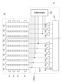
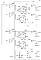
- FIG. 3 is a diagram showing part of the circuit configuration of an output circuit and an example of a touch sensor
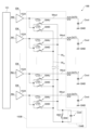
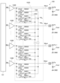
- FIG. 3 is a diagram showing an example of a circuit configuration of an output circuit including an intermediate potential supply section
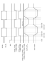
- 4 is a timing chart showing an example of potential transition of each signal in an output circuit
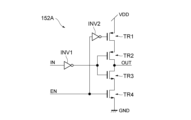
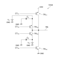
- FIG. 3 is a diagram showing a first example of a circuit configuration of a transmission driver
- FIG. 10 is a diagram showing a second example of the circuit configuration of a transmission driver
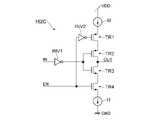
- FIG. 11 is a diagram showing a third example of the circuit configuration of a transmission driver
- FIG. 12 is a diagram showing a fourth example of the circuit configuration of the transmission driver
- FIG. 3 is a diagram showing part of the circuit configuration of an output circuit and an example of a touch sensor
- FIG. 3 is a diagram showing an example of a circuit configuration of an output circuit including an intermediate potential supply section
- 4 is a timing chart showing an example of potential transition of each signal in an output circuit
- FIG. 3 is a diagram showing a first example
- FIG. 12 is a diagram showing a fifth example of the circuit configuration of a transmission driver; 4 is a timing chart showing an example of potential transition of each signal in a transmission driver;
- FIG. 10 is a diagram showing an example of a circuit configuration of an output circuit including an intermediate potential supply section according to the second embodiment; 9 is a timing chart showing potential transition of each signal in the output circuit according to the second embodiment.
- FIG. 11 is a diagram showing an example of the circuit configuration of an output circuit including an intermediate potential supply section according to the third embodiment; 9 is a timing chart showing an example of potential transition of each signal in the output circuit according to the third embodiment.
- FIG. 11 is a timing chart showing potential transitions of signals in an output circuit according to a fifth embodiment;
- FIG. 14 is a diagram showing an example of a circuit configuration of an output circuit including an intermediate potential supply section according to a fourth embodiment
- FIG. 14 is a diagram showing an example of a circuit configuration of an output circuit including an intermediate potential supply section according to a fifth embodiment
- FIG. 10 is a diagram showing an example of a circuit configuration of a voltage source in a potential generator according to the third embodiment
- 4 is a flow chart showing an example of a series of processing flows of the output circuit according to the first embodiment
- FIG. 11 is a flow chart showing an example of the flow of a series of operations of the output circuit according to the third embodiment
- FIG. FIG. 16 is a flow chart showing an example of the flow of a series of operations of the output circuit according to the fifth embodiment
- this embodiment An embodiment of the present invention (hereinafter referred to as "this embodiment") will be described below with reference to the accompanying drawings.
- the same components and steps are denoted by the same reference numerals as much as possible in each drawing, and overlapping descriptions are omitted.
- FIG. 1 is a diagram showing an example of an electronic device 1 according to the first embodiment.
- the electronic device 1 is a computer owned by a user, and includes, for example, a tablet, a smart phone, a personal computer, and the like.
- a user can write pictures and characters on the electronic device 1 by holding the stylus 2 as a pen-shaped pointing device and moving the stylus 2 while pressing the pen tip against the touch surface of the electronic device 1 .
- the stylus 2 is, for example, an active electrostatic coupling (AES) electronic pen, and is configured to be able to communicate bidirectionally with the electronic device 1 .
- AES active electrostatic coupling
- the electronic device 1 detects the pointing position of the stylus 2 and performs various information processing according to the detection result. Specifically, the electronic device 1 transmits an uplink signal US to the stylus 2, detects the pointing position of the stylus 2 according to the reception result of the downlink signal DS from the stylus 2, and generates digital ink. processing and pointer display processing.
- the electronic device 1 includes a sensor controller 10 and a touch sensor 20 in addition to a host processor, memory, and communication module (none of which are shown).
- the touch sensor 20 is a capacitive sensor in which a plurality of detection electrodes are arranged in a plane.
- the touch sensor 20 includes, for example, a plurality of X-line electrodes (hereinafter referred to as "linear electrodes 21") for detecting the position of the X-axis of the sensor coordinate system, and a plurality of electrodes for detecting the position of the Y-axis.
- Y line electrodes hereinafter referred to as “linear electrodes 22"
- the linear electrodes 21 and 22 may be composed of a transparent conductive material containing ITO (Indium Tin Oxide), or may be composed of a wire mesh sensor.
- the touch sensor 20 may be a self-capacitance sensor in which block-shaped electrodes are arranged in a two-dimensional lattice instead of the above-described mutual capacitance sensor.
- the sensor controller 10 includes an MCU (Micro Controller Unit) 11, a control circuit 12, a transmission circuit 13, a reception circuit 14, an output circuit 15, a detection circuit 16, and selection circuits 17 and 18. be.
- MCU Micro Controller Unit
- the output circuit 15 selects one of the plurality of linear electrodes 22 or a plurality of electrodes adjacent to each other, and amplifies the input signal transmitted from the control circuit 12 to a predetermined voltage. It is a circuit for outputting the output signal to the linear electrode 22 as an output signal. Further, the detection circuit 16 is a circuit that selects one of the plurality of linear electrodes 21 or a plurality of mutually adjacent linear electrodes 21 based on an instruction from the control circuit 12 .
- the selection circuit 17 is, for example, a multiplexer, and is a circuit for switching whether the linear electrodes 22 selected by the output circuit 15 are used for reception or for transmission.
- the selection circuit 17 connects the linear electrode 22 selected by the output circuit 15 to the reception circuit 14 via the selection circuit 18 when the selection signal SELY output from the control circuit 12 is in the low state "0".
- the selection circuit 17 supplies the input signal input from the control circuit 12 to the linear electrodes 22 selected by the output circuit 15 when the selection signal SELY is in the high state “1”.
- the selection circuit 18 is, for example, a multiplexer, and receives a signal input from the linear electrode 22 selected by the output circuit 15 via the selection circuit 17, or a signal input from the linear electrode 21 selected by the detection circuit 16. and outputs the selected signal to the receiving circuit 14 .
- the selection circuit 18 connects the linear electrode 22 selected by the output circuit 15 to the reception circuit 14 when the selection signal SELX output from the control circuit 12 is in a low state.
- the selection circuit 18 connects the linear electrode 22 selected by the output circuit 15 via the selection circuit 17 to the reception circuit 14 when the selection signal SELX is in a high state.
- the electronic device 1 has the following four types of modes, and the control circuit 12 controls each circuit in the sensor controller 10 while switching these modes in the following order. Each will be described in detail below.
- the first mode is a mode that detects the position of the finger.
- the control circuit 12 sets the selection signal SELY to a high state and the selection signal SELX to a low state. That is, the transmission signal output from the control circuit 12 via the output circuit 15 is supplied to the linear electrode 22 selected by the output circuit 15 , and the touch sensor 20 transmits a touch detection signal. Also, the linear electrodes 21 selected by the detection circuit 16 are connected to the reception circuit 14 .
- the MCU 11 reads the change in the detection signal due to the contact of the finger on the sensor surface and calculates the coordinate position of the finger.
- the second mode is a mode in which an uplink signal US is transmitted to the stylus 2.
- the control circuit 12 supplies a transmission signal output from the control circuit 12 via the output circuit 15 to the linear electrodes 22 selected by the output circuit 15 by setting the selection signal SELY to a high state.
- An uplink signal US is transmitted from the touch sensor 20 .
- the output circuit 15 may select an electrode in the vicinity of the linear electrode 22 pointed by the stylus 2 and transmit the uplink signal US, or the output circuit 15 may select all of the linear electrodes 22 . electrodes may be simultaneously selected to transmit the trigger signal US_trg.
- a third mode is a mode in which the position of the stylus 2 is detected by detecting the position signal DS_pos transmitted by the stylus 2 .
- the control circuit 12 sets the selection signal SELY to a low state so that the linear electrodes 22 selected by the output circuit 15 are connected to the reception circuit 14 via the selection circuit 17 .
- the control circuit 12 sets the selection signal SELX to the low state to connect the linear electrode 21 selected by the detection circuit 16 to the reception circuit 14 .
- the detection circuit 16 selects a plurality of linear electrodes 21 centering on the linear electrode 21 closest to the pointing position of the stylus 2, for example, five linear electrodes 21, one by one.
- the MCU 11 reads the data output from the receiving circuit 14 as a signal level value.
- the MCU 11 calculates the X-axis coordinates of the stylus 2 from the signal level distribution for the selected linear electrodes 21 .
- the control circuit 12 sets the selection signal SELX to a high state and connects the linear electrode 22 selected by the output circuit 15 to the reception circuit 14 .
- the linear electrodes 22 selected by the output circuit 15 are sequentially selected one by one from a plurality of linear electrodes 22 centered on the linear electrode 22 closest to the pointing position of the stylus 2, for example, five linear electrodes 22.
- the MCU 11 reads the data output from the receiving circuit 14 as a signal level value.
- the MCU 11 calculates the Y-axis coordinates of the stylus 2 from the signal level distribution for the selected linear electrodes 22 .
- a fourth mode is a mode for receiving the data signal DS_res transmitted by the stylus 2 .
- Either the linear electrode 21 or the linear electrode 22 may be used when the data signal DS_res is received, but the case where the data signal DS_res is received using the linear electrode 21 will be described here.
- the control circuit 12 connects the linear electrode 21 selected by the detection circuit 16 to the reception circuit 14 by setting the selection signal SELX to a low state. Further, the control circuit 12 is operated so that the detection circuit 16 simultaneously selects a plurality of, for example, three linear electrodes 21 centering on the linear electrode 21 closest to the pointed position of the stylus 2 . In this state, MCU 11 periodically reads the output from receiving circuit 14 .
- the selection signal SELY should be set to the low state and the selection signal SELX should be set to the high state.
- control circuit 12 is configured to transmit and receive signals using the same touch sensor 20 for transmission and reception.
- Other configurations in the electronic device 1 shown in FIG. 1 will be described below.
- the MCU 11 is a microprocessor that has ROM and RAM inside and operates based on a predetermined program, and controls the control circuit 12 to output each signal as described above. At the same time, the digital data output from the receiving circuit 14 is read and processed.
- the control circuit 12 is a logic circuit for accurately outputting each signal at designated timing based on instructions from the MCU 11 .
- FIG. 2 is a diagram showing part of the circuit configuration of the output circuit 15 and an example of the touch sensor 20 according to this embodiment.
- the output circuit 15 includes a driver selection circuit 151, a plurality of transmission drivers 152, and an intermediate potential supply section 153.
- a driver selection circuit 151 selects some of a plurality of transmission drivers 152 that transmit signals to the linear electrodes 22 according to instructions from the control circuit 12, and uses data signals transmitted from the transmission circuit 13 as a plurality of input signals IN. , outputs each input signal IN to the corresponding transmission driver 152 .
- One transmission driver 152 is provided for one linear electrode 22 .
- the transmission driver 152 amplifies the input signal IN input from the driver selection circuit 151 to a potential difference that allows the signal to be transmitted from the linear electrodes 22, and outputs the amplified signal as the transmission signal OUT to the output signal line Wout. to the corresponding linear electrode 22.
- the potential difference with which a signal can be transmitted from the linear electrode 22 is 5 V, which is a potential of, for example, 0 V (first potential) at the low level and a potential of about 9 V (second potential) at a high level of 5 V or higher.
- the potential difference is about 9V.
- the intermediate potential supply section 153 generates an intermediate potential that is a potential between high level and low level.
- the intermediate potential is, for example, a potential obtained by adding the values of the high level and the low level and dividing the result by two.
- the intermediate potential supply unit 153 is selected by the driver selection circuit 151 at the timing when the potential of the output signal line Wout transitions from high level to low level or at the timing when the potential of the output signal line Wout transitions from low level to high level.
- the generated intermediate potential is supplied to the output signal line Wout corresponding to the transmission driver 152 .
- the intermediate potential supply unit 153 stops supplying the intermediate potential to the output signal line Wout at the timing when the potential of the output signal line Wout to which the intermediate potential is to be supplied reaches the intermediate potential.
- FIG. 3 is a diagram showing an example of the circuit configuration of the output circuit 15 including the intermediate potential supply section 153A according to this embodiment.
- the output circuit 15A includes a driver selection circuit 151, a plurality of transmission drivers 152A, and an intermediate potential supply section 153A.
- the driver selection circuit 151 selects n+1 transmission drivers 152A.
- n is a positive integer.
- the linear electrode 22 has a capacitive element Cout as a load capacitance.
- the capacitance of the capacitive element Cout is, for example, approximately 1200 pF.
- the driver selection circuit 151 selects n+1 transmission drivers 152A and transmits the input signal IN to the selected transmission drivers 152A.
- the input signal IN0 is input to the 0th transmission driver 152A.
- An input signal IN1 is input to the first transmission driver 152A, an input signal INn-1 is input to the nth transmission driver 152A, and an input signal INn is input to the n+1th transmission driver 152A.
- the transmission driver 152A is a driver with an output control function added to the transmission driver 152 described above.
- the transmission driver 152A sets the mode to the output mode or the stop mode according to the output control signal EN output from the control circuit 12.
- FIG. In the output mode the transmission driver 152A amplifies the input signal IN to a potential difference that allows the signal to be transmitted from the linear electrode 22, and transmits the amplified signal as the transmission signal OUT via the output signal line Wout. A signal OUT is sent to the corresponding linear electrode 22 .
- the transmission driver 152A sets the output state to the high impedance state "Hi-Z" and stops the transmission of the transmission signal OUT.
- the intermediate potential supply section 153A includes a potential generation section 154A, a plurality of short circuit control elements SW, a short circuit control element SWr, a reset voltage source Vrst, and a short circuit signal line Ws.
- the potential generator 154A is configured including, for example, a voltage source Vmid and a capacitive element Cext.
- the voltage source Vmid is, for example, a voltage source that generates an intermediate potential.
- the potential generator 154A generates an intermediate potential, for example, 4.5 V, and applies the generated intermediate potential to the short-circuit signal line Ws.
- the capacitive element Cext is, for example, a capacitor having a capacitance of about 1 uF, one end of which is connected to the short-circuit signal line Ws, and the other end of which is connected to the reference line GND.
- the capacitive element Cext charges or discharges electric charges according to the potential supplied to the short-circuit signal line Ws, thereby stabilizing the potential of the short-circuit signal line Ws.
- the potential generator 154A includes the voltage source Vmid and the capacitive element Cext, but may be configured with only one of the voltage source Vmid and the capacitive element Cext.
- the short-circuit control element SWr is, for example, a switch element or a transistor, and has one end connected to the short-circuit signal line Ws and the other end connected to one end of the reset voltage source Vrst.
- the short-circuit control element SWr short-circuits or opens both ends according to the reset signal RST output from the control circuit 12 . Specifically, the short-circuit control element SWr short-circuits both ends when the reset signal RST is in a high state, and opens both ends when the reset signal RST is in a low state.
- the reset voltage source Vrst is a voltage source that generates an initial potential (eg, 4.5 V), and supplies the initial potential generated when the short-circuit control element SWr is short-circuited to the short-circuit signal line Ws.
- the reset voltage source Vrst has one end connected to the other end of the short-circuit control element SWr and the other end connected to the reference line GND.
- the short-circuit control element SW is, for example, a switch element or a transistor, and has one end connected to the corresponding output signal line Wout and the other end connected to the short-circuit signal line Ws.
- the short-circuit control element SW is provided for each transmission driver 152A and short-circuits or opens both ends according to a control signal CT output from the control circuit 12 . Specifically, the short circuit control element SW short-circuits both ends when the state of the control signal CT is high, and opens both ends when the state of the control signal CT is low.
- the control circuit 12 operates at the timing when any one of the input signals IN0 to INn transitions from the high state to the low state, or at the timing when the state changes from the low state to the high state.
- the state of the transmission driver 152A is controlled to be in a high impedance state
- the short circuit control element SW is controlled to be in a short circuit state.
- the output signal line Wout and the short-circuit signal line Ws of each transmission driver 152A are short-circuited, so that the output signal line Wout at the high level is connected to the output signal line Wout at the low level via the short-circuit signal line Ws.
- a potential is supplied to Wout and the capacitive element Cext. Further, a potential is supplied from the voltage source Vmid and the capacitive element Cext to the output signal line Wout whose potential is at a low level through the short-circuit signal line Ws.
- the control circuit 12 controls the state of the transmission driver 152A to the output state at the timing when the potential of each output signal line Wout, the short-circuit signal line Ws, and one end of the capacitive element Cext reaches the intermediate potential, and the short-circuit control is performed.
- the element SW is controlled to be open.
- the potential of each output signal line Wout transitions to a high level or a low level by the corresponding transmission driver 152A, and transmission signals OUT0, OUT1, OUTn ⁇ 1 and OUTn are transmitted via the linear electrodes 22.
- FIG. 5A is a diagram showing an example of the circuit configuration of the transmission driver 152A according to this embodiment.
- the transmission driver 152A includes, for example, logic NOT circuits INV1 and INV2, transistors TR1, TR2, TR3 and TR4, a power supply line VDD, and a reference line GND.
- the logical NOT circuit INV2 is, for example, an inverter circuit including a transistor, performs a logical NOT operation on the output control signal EN input from the control circuit 12, and outputs the signal obtained by the operation to the gate of the transistor TR1. output to the terminal.
- the transistor TR1 is, for example, a P-type MOS transistor, and has a gate terminal connected to the output terminal of the logical NOT circuit INV2, a source terminal connected to the power supply line VDD, and a drain terminal connected to the source terminal of the transistor TR2.
- the transistor TR1 supplies or stops the supply of the potential (high level) of the power supply line VDD to the source terminal of the transistor TR2 according to the signal output from the logic NOT circuit INV2. Specifically, when the state of the signal output from the logic NOT circuit INV2 is low, the transistor TR1 supplies the potential (high level) of the power supply line VDD to the source terminal of the transistor TR2. When the state of the signal output from INV2 is high, the supply is stopped.
- the transistor TR4 is, for example, an N-type MOS transistor, and has a gate terminal connected to the control circuit 12, a source terminal connected to the reference line GND, and a drain terminal connected to the source terminal of the transistor TR3.
- the transistor TR4 extracts or stops the extraction from the source terminal of the transistor TR3 toward the reference line GND. Specifically, when the state of the output control signal EN is high, the transistor TR4 extracts electric charges from the source terminal of the transistor TR3 toward the reference line GND, and when the state of the output control signal EN is low, the transistor TR4 draws electric charges from the source terminal of the transistor TR3. , stop drawing the charge.
- the logical NOT circuit INV1 is, for example, an inverter circuit including transistors, performs a logical NOT operation on the input signal IN input from the driver selection circuit 151, and outputs the signal obtained by the operation to the transistors TR2 and TR3. output to the gate terminal of
- the transistor TR2 is, for example, a P-type MOS transistor, has a gate terminal connected to the output terminal of the logical NOT circuit INV1, a source terminal connected to the drain terminal of the transistor TR1, and a drain terminal connected to the drain terminal of the transistor TR3 and the output signal line. Wout.
- the transistor TR2 supplies or stops the supply of the potential of the drain terminal of the transistor TR1 to the output signal line Wout according to the signal output from the logic NOT circuit INV1. Specifically, when the state of the signal output from the logic NOT circuit INV1 is low, the transistor TR2 supplies the potential of the drain terminal of the transistor TR1 to the output signal line Wout, while outputting from the logic NOT circuit INV1 If the state of the signal received is in the high state, the supply is stopped.
- the transistor TR3 is, for example, an N-type MOS transistor, has a gate terminal connected to the output terminal of the logical NOT circuit INV1, a source terminal connected to the drain terminal of the transistor TR4, and a drain terminal connected to the drain terminal of the transistor TR2 and the output signal line. Wout.
- the transistor TR3 extracts or stops extracting charges from the output signal line Wout toward the drain terminal of the transistor TR4 according to the signal output from the logical NOT circuit INV1. Specifically, when the state of the signal output from the logic NOT circuit INV1 is in a high state, the transistor TR3 extracts electric charges from the output signal line Wout toward the drain terminal of the transistor TR4, while at the same time When the state of the output signal is low, the extraction is stopped.
- a power supply line VDD supplies a high-level potential supplied from a voltage source (not shown) to the transmission driver 152A.
- the high-level potential is a potential of, for example, about 9V, which is 5V or higher.
- the reference line GND supplies a low-level potential to the transmission driver 152A.
- the low-level potential is, for example, a potential of 0V.
- the transmission driver 152A configured as described above amplifies the input signal IN to a potential difference at which the signal can be transmitted from the linear electrode 22. The amplified signal is transmitted to the output signal line Wout as the transmission signal OUT.
- the transmission driver 152A sets the output state to the high impedance state "Hi-Z" and stops the transmission of the transmission signal OUT.
- FIG. 5C is a diagram showing another example of the circuit configuration of the transmission driver 152 according to this embodiment.
- the transmission driver 152C includes, for example, current sources I0 and I1 in addition to the configuration of the transmission driver 152A described above.
- the description of the circuit configuration of the transmission driver 152C the description of the configuration similar to that of the transmission driver 152A is omitted.
- the current source I0 is, for example, a current mirror circuit including a MOS transistor, and limits the current flowing from the power supply line VDD toward the source terminal of the transistor TR1 to a constant current value.
- the current source I1 is, for example, a current mirror circuit including a MOS transistor, and limits the current flowing from the source terminal of the transistor TR4 toward the reference line GND to a constant current value.
- the transmission driver 152C configured as described above limits the current flowing from the power supply line VDD to the transmission driver 152C and the current flowing from the transmission driver 152C to the reference line GND to a constant current value, thereby increasing the potential of the transmission signal OUT. transition as compared to transmit driver 152A. As a result, the EMI characteristics of the transmission driver 152C are improved compared to the transmission driver 152A by reducing the high frequency components of the transmission driver 152C.
- FIG. 5D is a diagram showing another example of the circuit configuration of the transmission driver 152 according to this embodiment.
- the transmission driver 152D includes, for example, an OR circuit OR, an AND circuit AND, and delay circuits DL0 and DL1 in addition to the configuration of the transmission driver 152A described above.
- the description of the circuit configuration of the transmission driver 152D the description of the configuration similar to that of the transmission driver 152A is omitted.
- the logical sum circuit OR includes, for example, a MOS transistor, performs a logical sum operation on the output signal of the logical NOT circuit INV1 and the trigger signal TGn output from the delay circuit DL1, and delays the result of the operation. Output to circuit DL0.
- the logical product circuit AND includes, for example, a MOS transistor, performs a logical product operation on the output signal of the logical NOT circuit INV1 and the trigger signal TGp output from the delay circuit DL0, and delays the result of the operation. Output to circuit DL1.
- the delay circuit DL0 is a buffer circuit including, for example, MOS transistors.
- the delay circuit DL0 delays the output signal of the OR circuit OR by the delay time td, and outputs the delayed signal as the trigger signal TGp to the gate terminal of the transistor TR2 and the AND circuit AND.
- the delay circuit DL1 is a buffer circuit including, for example, MOS transistors.
- the delay circuit DL1 delays the output signal of the AND circuit AND by the delay time td, and outputs the delayed signal as the trigger signal TGn to the gate terminal of the transistor TR3 and the OR circuit OR.
- the OR circuit OR, the AND circuit AND, the drain terminal and the source terminal of the transistor TR2, and the drain terminal and the source terminal of the transistor TR3 are simultaneously in a conductive state. Therefore, it is possible to prevent the generation of through current from the power supply line VDD to the reference line GND via the transistors TR1 to TR4.
- FIG. 6 is a timing chart showing the potential transition of each signal in the transmission driver 152D according to this embodiment. Although not shown, the state of the output control signal EN is assumed to be high level at any time.
- the driver selection circuit 151 changes the state of the input signal IN from low to high.
- the logical NOT circuit INV1 performs a logical NOT operation on the input signal IN (high state), and outputs a low state signal as a result of the operation to the OR circuit OR and AND circuit AND.
- the logical product circuit AND performs a logical product operation on the trigger signal TGp (high state) and the signal (low state) output from the logical NOT circuit INV1, and the signal that has become low as a result of the operation is is output to the delay circuit DL1.
- the delay circuit DL1 receives the low-state signal from the AND circuit AND and delays the signal by the delay time td.
- the delay circuit DL1 uses the delayed result as the trigger signal TGn and outputs the low-state trigger signal TGn to the gate terminal of the transistor TR3 and the OR circuit OR.
- the transistor TR3 receives the low-state trigger signal TGn and makes the drain terminal and the source terminal non-conductive. As a result, both the drain terminal and the source terminal of the transistor TR2 and the drain terminal and the source terminal of the transistor TR3 are disconnected, so that the state of the output signal line Wout becomes a high impedance state.
- the OR circuit OR performs a logical sum operation on the trigger signal TGn (low state) and the signal (low state) output from the logical NOT circuit INV1, and the signal that has become low as a result of the operation is is output to the delay circuit DL0.
- the delay circuit DL0 receives the low-state signal from the OR circuit OR and delays the signal by the delay time td.
- the delay circuit DL0 uses the delayed result as the trigger signal TGp and outputs the low-state trigger signal TGp to the gate terminal of the transistor TR2 and the AND circuit AND.
- the transistor TR2 receives the low-state trigger signal TGp, and conducts between the drain terminal and the source terminal. As a result, a high level potential is supplied from the power supply line VDD to the output signal line Wout via the transistors TR1 and TR2, and the potential of the transmission signal OUT transitions to a high level.
- the driver selection circuit 151 changes the state of the input signal IN from high to low.
- the logical NOT circuit INV1 performs a logical NOT operation on the input signal IN (low state), and outputs a signal in a high state as a result of the operation to the OR circuit OR and AND circuit AND.
- the OR circuit OR performs a logical sum operation on the trigger signal TGn (low state) and the signal (high state) output from the logic NOT circuit INV1, and the signal that has become high as a result of the operation is is output to the delay circuit DL0.
- the delay circuit DL0 receives the high-state signal from the OR circuit OR and delays the signal by the delay time td.
- the delay circuit DL0 uses the delayed result as the trigger signal TGp and outputs the high-state trigger signal TGp to the gate terminal of the transistor TR2 and the AND circuit AND.
- the transistor TR2 receives the high-state trigger signal TGp, and renders the drain terminal and the source terminal non-conductive. As a result, both the drain terminal and the source terminal of the transistor TR2 and the drain terminal and the source terminal of the transistor TR3 are disconnected, so that the state of the output signal line Wout becomes a high impedance state.
- the logical product circuit AND performs a logical product operation on the trigger signal TGp (high state) and the signal (high state) output from the logical NOT circuit INV1, and outputs a high state signal as a result of the operation. is output to the delay circuit DL1.
- delay circuit DL1 receives the signal in the high state from AND circuit AND and delays the signal by delay time td.
- the delay circuit DL1 uses the delayed result as the trigger signal TGn and outputs the high-state trigger signal TGn to the gate terminal of the transistor TR3 and the OR circuit OR.
- the transistor TR3 receives the trigger signal TGn in the high state and conducts between the drain terminal and the source terminal. As a result, charges are extracted from the output signal line Wout toward the reference line GND via the transistors TR1 and TR2, and the potential of the transmission signal OUT transitions to low level.
- FIG. 5E is a diagram showing another example of the circuit configuration of the transmission driver 152 according to the first embodiment of the invention.
- the transmission driver 152E has a configuration in which the configuration of the transmission driver 152D is added to the configuration of the transmission driver 152C described above. Therefore, description of the circuit configuration of the transmission driver 152E is omitted.
- the transmission driver 152E is configured by combining the configurations of the transmission drivers 152C and 152D, the EMI characteristics are improved compared to the transmission driver 152A due to the reduction of high frequency components. It is possible to prevent the generation of through current from the power supply line VDD to the reference line GND via the transistors TR1 to TR4.
- FIG. 4 is a timing chart showing potential transition of each signal in the output circuit 15A according to the present embodiment.
- the control circuit 12 opens both ends of the short-circuit control element SWr by setting the state of the reset signal RST to the low state. As a result, the supply of the initial potential from the reset voltage source Vrst to the short-circuit signal line Ws is stopped.
- the driver selection circuit 151 causes the states of the input signals IN0 and INn ⁇ 1 to transition from the low state to the high state, and causes the states of the input signals IN1 and INn to transition from the high state to the low state.
- Input signals IN0, IN1, INn-1 and INn are applied to the corresponding transmit drivers 152A.
- the control circuit 12 changes the state of the output control signal EN from the high state to the low state, and sets the mode of each transmission driver 152A to the stop mode.
- the control circuit 12 changes the state of the control signal CT from the low state to the high state and outputs the control signal CT to each short circuit control element SW, thereby short-circuiting both ends of each short circuit control element SW. do.
- the output signal lines Wout are short-circuited via the short-circuit control elements SW whose both ends are short-circuited.
- the control circuit 12 causes the state of the output control signal EN to transition from the low state to the high state, and sets the mode of each transmission driver 152A to the output mode.
- the control circuit 12 changes the state of the control signal CT from the high state to the low state and outputs the control signal CT to each short circuit control element SW, thereby short-circuiting both ends of each short circuit control element SW. do.
- the short-circuit state between the output signal lines Wout is released.
- the electric charges are supplied from the corresponding transmission driver 152A, so that the electric potentials of the transmission signals OUT0 and OUTn-1 transition from the intermediate electric potential to the high level, while electric charges are extracted from the corresponding transmission driver 152A.
- the potentials of the transmission signals OUT1 and OUTn transition from the intermediate potential to the low level.
- the control circuit 12 changes the state of the output control signal EN from the high state to the low state, and sets the mode of each transmission driver 152A to the stop mode.
- the control circuit 12 changes the state of the control signal CT from the low state to the high state and outputs the control signal CT to each short circuit control element SW, thereby opening both ends of each short circuit control element SW. do.
- the potentials of the transmission signals OUT0, OUT1, OUTn ⁇ 1, and OUTn become intermediate potentials, as at time t41.
- the control circuit 12 causes the state of the output control signal EN to transition from the low state to the high state, and sets the mode of each transmission driver 152A to the output mode.
- the control circuit 12 changes the state of the control signal CT from the high state to the low state and outputs the control signal CT to each short circuit control element SW, thereby short-circuiting both ends of each short circuit control element SW. do.
- the short-circuit state between the output signal lines Wout is released.
- the potentials of the transmission signals OUT0 and OUTn-1 transition from the intermediate potential to the low level due to the supply of charges from the corresponding transmission driver 152A.
- the potentials of the transmission signals OUT1 and OUTn transition from the intermediate potential to the high level.
- FIG. 15 is a flow chart showing a series of processes of the output circuit 15A according to the first embodiment.
- Step SP10 The transmission driver 152A amplifies the input signal IN input from the driver selection circuit 151 to a potential difference that allows the signal to be transmitted from the linear electrode 22, and converts the amplified signal into the transmission signal OUT. It transmits to the corresponding output signal line Wout. Then, the process moves to step SP12.
- Step SP12 The control circuit 12 determines whether the signal waveform of the transmission signal OUT rises from low level to high level or falls from high level to low level. If the determination is affirmative, the process proceeds to step SP14. On the other hand, if the determination is negative, the series of processing ends.
- Step SP14 The control circuit 12 sets the mode of the transmission driver 152A to the stop mode. As a result, the state of the output of the transmission driver 152A becomes a high impedance state. Then, the process moves to step SP16.
- Step SP16 The control circuit 12 controls to short-circuit both ends of each short-circuit control element SW.
- the output signal lines Wout are short-circuited to each other via the short-circuit signal line Ws, and from the potential generator 154A and the output signal line Wout whose potential is high level, via the short-circuit signal line Ws, the potential is low.
- a potential is supplied to a certain output signal line Wout.
- the potentials of the short-circuit signal line Ws and each output signal line Wout become intermediate potentials. Then, the process moves to step SP18.
- the control circuit 12 determines which short-circuit signal line Ws each output signal line Wout is to be connected to.
- the short-circuit control element SW corresponding to the signal line Ws is controlled to be short-circuited.
- Step SP18 The control circuit 12 controls to open both ends of each short circuit control element SW. As a result, the short circuit between the output signal lines Wout is released. Then, the process moves to step SP20.
- Step SP20 The control circuit 12 sets the mode of the transmission driver 152A to the output mode. Thereby, a high level or a low level is supplied from the transmission driver 152A to the output signal line Wout.
- the potential of the transmission signal OUT transitions from an intermediate potential to a high level or a low level according to the potential of the output signal line Wout.
- the sensor controller 10 is connected to the touch sensor 20 in which the plurality of linear electrodes 21 and 22 are arranged in a plane.
- the sensor controller 10 generates a signal waveform that transitions between a first potential (low level) and a second potential (high level) higher than the first potential, and outputs a plurality of transmission signals OUT as a transmission signal OUT.
- It includes a driver 152A, a plurality of output signal lines Wout for outputting the transmission signal OUT from the corresponding transmission driver 152A to the corresponding linear electrode 22, and a voltage source Vmid or capacitive element Cext separate from the transmission driver 152.
- the potential generator 154A is provided, and potential generation is performed at first timings (times t41, t43, t45 and t47) when the potential of the signal waveform starts transitioning from high level to low level or from low level to high level. and an intermediate potential supply section 153A that supplies an intermediate potential between the high level and the low level to the output signal line Wout by outputting a voltage from the section 154A.
- the sensor controller 10 outputs the intermediate potential to the output signal line Wout from the intermediate potential supply unit 153A having the potential generator 154A having the voltage source Vmid or the capacitive element Cext, which is separate from the transmission driver 152A.
- the intermediate potential can be stably supplied to the output signal line Wout at the required timing. Therefore, according to the present invention, the sensor controller 10 can suppress through current and reduce power consumption compared to the conventional configuration.
- the potential generator 154A is a capacitive element Cext connected to at least one of the plurality of output signal lines Wout.
- the sensor controller 10 can stably supply an intermediate potential from the capacitive element Cext to each output signal line Wout when the output state of each transmission driver 152A is in a high impedance state. can.
- the output side of the potential generator 154A is connected to two or more of the plurality of output signal lines Wout.
- the sensor controller 10 can suppress through current and reduce power consumption compared to the conventional configuration.
- the sensor controller 10 includes the control circuit 12 that transmits the control signal CT, and the transmission driver 152A has an output mode for outputting the transmission signal OUT and a stop mode for setting the output state to a high impedance state.
- the control circuit 12 controls the transmission driver 152A to enter the stop mode, and at a second timing (time t42, t44, At t46 and t48), the transmission driver 152 is controlled to be in the output mode.
- the sensor controller 10 sets the state of the output of each transmission driver 152A to the high impedance state, and sets the period during which the intermediate potential supply unit 153A supplies the intermediate potential stably to each output signal line Wout. By providing, power consumption can be reduced.
- both ends of the intermediate potential supply section 153A are shorted or opened according to the control signal CT, one end is connected to the corresponding output signal line Wout, and the other end is connected to the output side of the potential generation section 154A.
- the control circuit 12 controls the short circuit control elements SW to short circuit at a first timing, and controls the short circuit control elements SW to open at a second timing.
- the sensor controller 10 can suppress through current and reduce power consumption compared to the conventional configuration.
- the second potential (high level) is a potential of 5 V or higher, and the second potential (high level) is a potential higher than the first potential (low level).
- the sensor controller 10 can reduce power consumption even when using the transmission driver 152A driven at a voltage of 5V or higher.
- FIG. 7 is a diagram showing an example of a circuit configuration of an output circuit 15B including an intermediate potential supply section 153B according to the second embodiment.
- the output circuit 15B includes a driver selection circuit 151, a plurality of transmission drivers 152A, and an intermediate potential supply section 153B.
- the driver selection circuit 151 selects n+1 transmission drivers 152A.
- the linear electrode 22 has a capacitive element Cout as a load capacitance.
- the capacitance of the capacitive element Cout is, for example, approximately 1200 pF.
- the driver selection circuit 151 and the transmission driver 152A are the same as those described in the first embodiment, so description thereof will be omitted.
- the intermediate potential supply section 153B includes a potential generation section 154B, a plurality of short circuit control elements SWU and SWD, short circuit signal lines Wsu and Wsd, a short circuit control element SWr, and a capacitive element Cext.
- the potential generator 154B is configured including, for example, a capacitive element Cext.
- the capacitive element Cext is, for example, a capacitor having a capacitance of approximately 1 uF, one end of which is connected to the short-circuit signal line Wsu, and the other end of which is connected to the short-circuit signal line Wsd.
- the capacitive element Cext charges or discharges according to the potential difference between the potentials supplied to the short-circuit signal lines Wsu and Wsd, thereby stabilizing the potentials of the short-circuit signal lines Wsu and Wsd.
- the short-circuit control element SWr is, for example, a switch element or a transistor, and short-circuits or opens the short-circuit signal line Ws and the reset voltage source Vrst according to the reset signal RST output from the control circuit 12 .
- the short-circuit control element SWr has one end connected to the short-circuit signal line Wsu and the other end connected to one end of the short-circuit signal line Wsd.
- the short-circuit control element SWr short-circuits the short-circuit signal lines Wsu and Wds when short-circuited, and releases the short-circuit of the short-circuit signal lines Wsu and Wds when opened.
- the short-circuit control element SWU is, for example, a switch element or a transistor, and has one end connected to the corresponding output signal line Wout and the other end connected to the short-circuit signal line Wsu.
- the short-circuit control element SWU is provided for each transmission driver 152A, and short-circuits or opens both ends according to a control signal CTU output from the control circuit 12 to each short-circuit control element SWU.
- the short-circuit control element SWU short-circuits both ends when the control signal CTU is in a high state, and opens both ends when the control signal CTU is in a low state.
- the short-circuit control element SWD is, for example, a switch element or a transistor, and has one end connected to the corresponding output signal line Wout and the other end connected to the short-circuit signal line Wsd.
- the short-circuit control element SWD is provided for each transmission driver 152A, and short-circuits or opens both ends according to a control signal CTD output from the control circuit 12 to each short-circuit control element SWD.
- the short-circuit control element SWD short-circuits both ends when the control signal CTD is in a high state, and opens both ends when the control signal CTD is in a low state.
- the control circuit 12 operates at the timing when any one of the input signals IN0 to INn transitions from the high state to the low state, or at the timing when the state changes from the low state to the high state. , controls the state of the transmission driver 152A to a high impedance state. Further, the control circuit 12 assigns a value according to a code (for example, an orthogonal code) to each transmission driver 152A, and determines to which of the short-circuit signal lines Wsu and Wsd the corresponding output signal line Wout is connected.
- a code for example, an orthogonal code
- the control circuit 12 determines to connect a certain output signal line Wout to the short-circuit signal line Wsu.
- the value of the orthogonal code corresponding to a certain output signal line Wout is "1" it is determined to connect the certain output signal line Wout to the short-circuit signal line Wsd. It is desirable that the code for determining the value to be assigned to each transmission driver 152A contain the value of "0" and the value of "1" at approximately the same rate.
- the control circuit 12 determines the output signal to be connected to the short-circuit signal line Wsu at the timing when any one of the input signals IN0 to INn transitions from the high state to the low state or from the low state to the high state.
- Short-circuit control element SWU corresponding to line Wout is controlled to be in a short-circuit state
- short-circuit control element SWD corresponding to output signal line Wout determined to be connected to short-circuit signal line Wsd is controlled to be in a short-circuit state.
- the output signal line Wout determined to be connected to the short-circuit signal line Wsu is connected to one end of the capacitive element Cext through the short-circuit signal line Wsu
- the output signal line Wout determined to be connected to the short-circuit signal line Wsd is connected to one end of the capacitive element Cext through the short-circuit signal line Wsd. are short-circuited with the other end of the capacitive element Cext.
- the control circuit 12 controls the state of the transmission driver 152A to the output state at the timing when the potentials of each of the output signal lines Wout, the short-circuit signal lines Wsu and Wsd, and both ends of the capacitive element Cext reach the intermediate potential.
- the short circuit control elements SWU and SWD are controlled to be open.
- the potential of each output signal line Wout transitions to a high level or a low level by the corresponding transmission driver 152A, and transmission signals OUT0, OUT1, OUTn ⁇ 1 and OUTn are transmitted via the linear electrodes 22.
- FIG. 8 is a timing chart showing potential transition of each signal in the output circuit 15B according to the second embodiment.
- the control circuit 12 connects the output signal line Wout corresponding to the transmission signals OUT0 and OUTn-1 to the short-circuit signal line Wsu, and connects the output signal line Wout corresponding to the transmission signals OUT1 and OUTn to the short-circuit signal line. It decides to connect to Wsd.
- the control circuit 12 opens both ends of the short circuit control element SWr by setting the state of the reset signal RST to the low state. As a result, the short-circuit state between the short-circuit signal lines Wsu and Wsd is released.
- the driver selection circuit 151 causes the states of the input signals IN0 and INn ⁇ 1 to transition from the low state to the high state, and causes the states of the input signals IN1 and INn to transition from the high state to the low state.
- Input signals IN0, IN1, INn-1 and INn are applied to the corresponding transmit drivers 152A.
- the control circuit 12 changes the state of the output control signal EN from the high state to the low state, and sets the mode of each transmission driver 152A to the stop mode. Also, at time t81, the control circuit 12 causes the states of the control signals CTU0, CTUn-1, CTD1 and CTDn to transition from the low state to the high state, so that the control signals CTU0, CTUn-1, CTD1 and CTDn are connected to the short circuit control element SWU0. , SWUn-1, SWD1 and SWDn to short-circuit both ends of the short circuit control elements SWU0, SWUn-1, SWD1 and SWDn.
- the output signal line Wout corresponding to the transmission signals OUT0 and OUTn-1 is short-circuited to one end of the potential generator 154B via the short-circuit control elements SWU0 and SWUn-1 whose both ends are short-circuited.
- the output signal line Wout corresponding to the transmission signals OUT1 and OUTn is short-circuited to the other end of the potential generator 154B via the short-circuit control elements SWD1 and SWDn whose both ends are short-circuited.
- the control circuit 12 causes the state of the output control signal EN to transition from the low state to the high state, and sets the mode of each transmission driver 152A to the output mode.
- the control circuit 12 causes the states of the control signals CTU0, CTUn-1, CTD1, and CTDn to transition from the high state to the low state, and the control signals CTU0, CTUn-1, CTD1, and CTDn are connected to the short-circuit control element SWU0. , SWUn-1, SWD1 and SWDn, both ends of the short circuit control elements SWU0, SWUn-1, SWD1 and SWDn are opened.
- the driver selection circuit 151 changes the states of the input signals IN0 and INn ⁇ 1 from high to low, and changes the states of the input signals IN1 and INn from low to high.
- Input signals IN0, IN1, INn-1 and INn are applied to the corresponding transmit drivers 152A.
- the control circuit 12 changes the state of the output control signal EN from the high state to the low state, and sets the mode of each transmission driver 152A to the stop mode.
- the control circuit 12 causes the states of the control signals CTU0, CTUn-1, CTD1, and CTDn to transition from the low state to the high state, and the control signals CTU0, CTUn-1, CTD1, and CTDn are connected to the short-circuit control element SWU0. , SWUn-1, SWD1 and SWDn to short-circuit both ends of the short circuit control elements SWU0, SWUn-1, SWD1 and SWDn.
- the output signal line Wout corresponding to the transmission signals OUT0 and OUTn-1 is short-circuited to one end of the potential generator 154B via the short-circuit control elements SWU0 and SWUn-1 whose both ends are short-circuited.
- the output signal line Wout corresponding to the transmission signals OUT1 and OUTn is short-circuited to the other end of the potential generator 154B via the short-circuit control elements SWD1 and SWDn whose both ends are short-circuited.
- the control circuit 12 causes the state of the output control signal EN to transition from the low state to the high state, and sets the mode of each transmission driver 152A to the output mode.
- the control circuit 12 causes the states of the control signals CTU0, CTUn-1, CTD1 and CTDn to transition from the high state to the low state, and the control signals CTU0, CTUn-1, CTD1 and CTDn are connected to the short circuit control element SWU0. , SWUn-1, SWD1 and SWDn, both ends of the short circuit control elements SWU0, SWUn-1, SWD1 and SWDn are opened.
- the potential generator 154B includes the capacitive element Cext
- the intermediate potential supply unit 153B includes the first short-circuit signal line Wsu connected to one end of the capacitive element Cext and the capacitor
- a second short-circuit signal line Wsd connected to the other end of the element Cext, both ends of which are short-circuited or opened according to the control signal CTU, one end of which is connected to the corresponding output signal line Wout, and the other end of which is the first short-circuit signal line
- the sensor controller 10 outputs an intermediate potential to the output signal line Wout from the intermediate potential supply unit 153B having the potential generation unit 154B having the capacitive element Cext.
- An intermediate potential can be stably supplied at required timing. Therefore, according to the present invention, the sensor controller 10 can suppress through current and reduce power consumption compared to the conventional configuration.
- the control circuit 12 determines to which of the first short-circuit signal line Wsu and the second short-circuit signal line Wsd the output signal line Wout is connected for each output signal line Wout. When it is decided to connect the signal line Wout to the first short-circuit signal line Wsu, the signal line Wout is short-circuited at the first timings (times t81, t83, t85 and t87), and is short-circuited at the second timings (times t82, t84, t86 and t88).
- the sensor controller 10 sets the state of the output of each transmission driver 152A to the high impedance state, and sets the period during which the intermediate potential supply unit 153A supplies the intermediate potential stably to each output signal line Wout. By providing, power consumption can be reduced.
- FIG. 9 is a diagram showing an example of the circuit configuration of an output circuit 15C including an intermediate potential supply section 153C according to the third embodiment.
- the output circuit 15C includes a driver selection circuit 151, a plurality of transmission drivers 152B, and an intermediate potential supply section 153C.
- the driver selection circuit 151 selects n+1 transmission drivers 152B.
- the linear electrode 22 has a capacitive element Cout as a load capacitance.
- the capacitance of the capacitive element Cout is, for example, approximately 1200 pF.
- the driver selection circuit 151 is the same as that of the first embodiment, so the description thereof will be omitted.
- the transmission driver 152B is a driver in which the output control function is removed from the transmission driver 152A described above.
- the transmission driver 152B amplifies the input signal IN to a potential difference that allows the signal to be transmitted from the linear electrode 22, uses the amplified signal as the transmission signal OUT, and outputs the transmission signal OUT via the output signal line Wout. It transmits to the linear electrode 22 which does.
- the intermediate potential supply section 153C includes a potential generation section 154A, a plurality of output control circuits 155A and 156A, a short-circuit signal line Ws, a short-circuit control element SWr, and a reset voltage source Vrst. Note that the potential generator 154A, the short-circuit control element SWr, and the reset voltage source Vrst are the same as those in the first embodiment, so description thereof will be omitted.
- the output control circuit 155A is provided for each transmission driver 152B, and according to the control signal CTD output from the control circuit 12 for each corresponding transmission driver 152B, the first direction from the corresponding output signal line Wout to the short-circuit signal line Ws. current path is made conducting or non-conducting.
- the output control circuit 155A includes a short control element SWD and a current control element DD.
- the short circuit control element SWD is, for example, a switch element or a transistor, and has one end connected to the corresponding output signal line Wout and the other end connected to the anode terminal of the current control element DD.
- the short-circuit control element SWD short-circuits or opens both ends according to the control signal CTD. Specifically, the short-circuit control element SWD short-circuits both ends when the control signal CTD is in a high state, and opens both ends when the control signal CTD is in a low state.
- the current control element DD is, for example, a diode, and conducts a current path in the first direction from the short-circuit control element SWD to the short-circuit signal line Ws, while the current flows in the direction from the short-circuit signal line Ws to the short-circuit control element SWD.
- the path becomes non-conducting.
- the current control element DD has an anode terminal connected to the short circuit control element SWD and a cathode terminal connected to the short circuit signal line Ws.
- the output control circuit 156A is provided for each transmission driver 152B, and operates in the second direction from the short-circuit signal line Ws to the corresponding output signal line Wout according to the control signal CTU output from the control circuit 12 for each corresponding transmission driver 152B. current path is made conducting or non-conducting.
- the output control circuit 156A includes a short control element SWU and a current control element DU.
- the short-circuit control element SWU is, for example, a switch element or a transistor, and has one end connected to the corresponding output signal line Wout and the other end connected to the cathode terminal of the current control element DU.
- the short-circuit control element SWU short-circuits or opens both ends according to the control signal CTU. Specifically, the short-circuit control element SWU short-circuits both ends when the control signal CTU is in a high state, and opens both ends when the control signal CTU is in a low state.
- the current control element DU is, for example, a diode, and has an anode terminal connected to the short-circuit signal line Ws and a cathode terminal connected to the short-circuit control element SWU.
- the current path in the second direction from the short-circuit signal line Ws to the short-circuit control element SWU is conductive, while the current path in the direction from the short-circuit control element SWU to the short-circuit signal line Ws is non-conductive. .
- the control circuit 12 controls the short-circuit control element SWU to the short-circuit state at the timing when the state of any one of the input signals IN0 to INn transitions from the low state to the high state. Further, the control circuit 12 controls the short-circuit control element SWD to the short-circuit state at the timing when the state of any one of the input signals IN0 to INn transitions from the high state to the low state.
- the current path in the first direction from the output signal line Wout whose potential is at a high level to the short-circuit signal line Ws becomes conductive
- the second current path from the short-circuit signal line Ws to the output signal line Wout whose potential is at a low level becomes conductive.
- the electric charge is supplied from the high-level output signal line Wout through the short-circuit signal line Ws to the capacitive element Cext and the low-level output signal line Wout.
- charges are supplied from the voltage source Vmid and the capacitive element Cext to the output signal line Wout whose potential is at the low level through the short-circuit signal line Ws.
- the potentials of each output signal line Wout and the short-circuit signal line Ws reach the intermediate potential.
- the current control element DU makes the current path in the second direction non-conductive at the timing when the potential of the short-circuit signal line Ws falls below the potential of the corresponding output signal line Wout.
- the current control element DD makes the current path in the first direction non-conductive at the timing when the potential of the corresponding output signal line Wout becomes lower than the potential of the short-circuit signal line Ws.
- FIG. 5B is a diagram showing an example of the circuit configuration of the transmission driver 152B according to this embodiment.
- the transmission driver 152B is a driver in which the output control function is removed from the transmission driver 152A described above.
- the transmission driver 152B has a configuration in which the transistors TR1 and TR4 are removed from the transmission driver 152A.
- the transmission driver 152B amplifies the input signal IN to a potential difference that allows the signal to be transmitted from the linear electrode 22, uses the amplified signal as the transmission signal OUT, and outputs the transmission signal OUT via the output signal line Wout. It transmits to the linear electrode 22 which does.
- FIG. 11A is a diagram showing another example of the circuit configuration of the output control circuit 156 according to the third embodiment.
- the output control circuit 156B includes a logical NOT circuit INV3, transistors TR5 and TR6, a short control element SWcu, and a voltage source VB.
- the logical NOT circuit INV3 is, for example, an inverter circuit composed of MOS transistors, performs a logical NOT operation on the control signal CTU output from the control circuit 12, and outputs the result of the operation to the short circuit control element SWcu and the transistor. Output to the gate terminal of TR5.
- the transistor TR5 is, for example, an N-type MOS transistor, has a gate terminal connected to the output terminal of the logic NOT circuit INV3, a source terminal connected to the reference line GND, and a drain terminal connected to the gate terminal of the transistor TR6 and the short circuit control element SWcu. is connected to the other end of the The transistor TR5 extracts charges from the gate terminal of the transistor TR6 toward the reference line GND according to the signal output from the logical NOT circuit INV3. Specifically, when the signal output from the logic NOT circuit INV3 is in a high state, the transistor TR5 extracts charges from the gate terminal of the transistor TR6 toward the reference line GND. The extraction of charges from the gate terminal of the transistor TR6 toward the reference line GND is stopped.
- the transistor TR6 is, for example, an N-type MOS transistor, and has a gate terminal connected to the drain terminal of the transistor TR5 and the other end of the short circuit control element SWcu, a source terminal connected to the corresponding output signal line Wout, and a drain terminal connected to the corresponding output signal line Wout. It is connected to the short-circuit signal line Ws.
- the transistor TR6 supplies the potential of the short-circuit signal line Ws to the corresponding output signal line Wout according to the potential of the gate terminal. Specifically, when the potential of the gate terminal is at the intermediate potential, the transistor TR6 supplies the potential of the short-circuit signal line Ws to the corresponding output signal line Wout. The potential supply from the line Ws to the corresponding output signal line Wout is stopped. Further, even when the potential of the short-circuit signal line Ws and the potential of the corresponding output signal line Wout are the same, the supply of the potential from the short-circuit signal line Ws to the corresponding output signal line Wout is stopped.
- a voltage source VB generates an intermediate potential and supplies the generated intermediate potential to one end of the short circuit control element SWcu.
- the voltage source VB has one end connected to the short circuit control element SWcu and the other end connected to the reference line GND.
- the short-circuit control element SWcu is, for example, a transistor or a switch element, and has one end connected to the voltage source VB and the other end connected to the drain terminal of the transistor TR5 and the gate terminal of the transistor TR6.
- the short-circuit control element SWcu short-circuits or opens both ends according to the signal output from the logic NOT circuit INV3. Specifically, the short-circuit control element SWcu shorts both ends when the signal output from the logic NOT circuit INV3 is in the low state, and opens both ends when the signal is in the high state.
- the output control circuit 156B configured as described above supplies the potential of the short-circuit signal line Ws to the corresponding output signal line Wout according to the control signal CTU output from the control circuit 12 . Specifically, when the control signal CTU is in a high state, the potential of the short-circuit signal line Ws is supplied to the corresponding output signal line Wout. supply of the potential from the corresponding output signal line Wout to the corresponding output signal line Wout. Further, even when the potential of the short-circuit signal line Ws and the potential of the corresponding output signal line Wout are the same, the output control circuit 156B stops supplying the potential from the short-circuit signal line Ws to the corresponding output signal line Wout. .
- FIG. 11B is a diagram showing another example of the circuit configuration of the output control circuit 155 according to the third embodiment.
- the output control circuit 155B includes transistors TR7 and TR8, a short circuit control element SWcd, and a voltage source VB.
- the transistor TR7 is, for example, a P-type MOS transistor, and has a gate terminal connected to the control circuit 12, a source terminal connected to the power supply line VDD, and a drain terminal connected to the gate terminal of the transistor TR8 and the other end of the short circuit control element SWcd. connected to The transistor TR7 supplies the potential (high level) of the power supply line VDD to the gate terminal of the transistor TR8 according to the control signal CTD output from the control circuit 12 . Specifically, the transistor TR7 supplies the potential of the power supply line VDD to the gate terminal of the transistor TR8 when the control signal CTD is in the low state, while supplying the potential of the power supply line VDD to the transistor TR6 when the signal is in the high state. The supply of potential to the gate terminal is stopped.
- the transistor TR8 is, for example, a P-type MOS transistor, has a gate terminal connected to the drain terminal of the transistor TR7 and the other end of the short-circuit control element SWcd, a source terminal connected to the corresponding output signal line Wout, and a drain terminal It is connected to the short-circuit signal line Ws.
- the transistor TR8 supplies the potential of the corresponding output signal line Wout to the short-circuit signal line Ws according to the potential of the gate terminal. Specifically, when the potential of the gate terminal is at the intermediate potential, the transistor TR8 supplies the potential of the corresponding output signal line Wout to the short-circuit signal line Ws. The supply of the potential from the output signal line Wout to the short-circuit signal line Ws is stopped. Further, even when the potential of the short-circuit signal line Ws and the potential of the corresponding output signal line Wout are the same, the supply of the potential from the corresponding output signal line Wout to the short-circuit signal line Ws is stopped.
- a voltage source VB generates an intermediate potential and supplies the generated intermediate potential to one end of the short circuit control element SWcd.
- the voltage source VB has one end connected to the short circuit control element SWcd and the other end connected to the reference line GND.
- the short-circuit control element SWcd is, for example, a transistor or a switch element, and has one end connected to the voltage source VB and the other end connected to the drain terminal of the transistor TR7 and the gate terminal of the transistor TR8.
- the short-circuit control element SWcd short-circuits or opens both ends according to the control signal CTD output from the control circuit 12 . Specifically, the short-circuit control element SWcd short-circuits both ends when the control signal CTD is in a high state, and opens both ends when the signal is in a low state.
- the output control circuit 155B configured as described above supplies the potential of the corresponding output signal line Wout to the short-circuit signal line Ws according to the control signal CTD output from the control circuit 12 . Specifically, when the state of the control signal CTD is high, the potential of the corresponding output signal line Wout is supplied to the short-circuit signal line Ws, and when the state of the control signal CTD is low, the corresponding output signal The supply of potential from the line Wout to the short-circuit signal line Ws is stopped. Further, even when the potential of the short-circuit signal line Ws and the potential of the corresponding output signal line Wout are the same, the output control circuit 155B stops supplying the potential from the corresponding output signal line Wout to the short-circuit signal line Ws. .
- FIG. 14 is a diagram showing an example of the circuit configuration of the voltage source Vmid according to the third embodiment.
- the voltage source Vmid includes transistors TRv1, TRv2, TRv3, and TRv4, capacitive elements Cu and Cd, voltage sources Vc1 and Vc2, a power supply line VDD, and a reference line GND. be.
- the transistor TRv1 is, for example, a P-type MOS transistor, and switches the potential of the power supply line VDD connected to the source terminal to the short-circuit signal line Ws connected to the drain terminal according to the control signal CTv1 input to the gate terminal from the control circuit 12. supply to Specifically, the transistor TRv1 supplies the potential of the power supply line VDD to the short-circuit signal line Ws when the control signal CTv1 is in the low state, and supplies the potential of the power supply line VDD when the control signal CTv1 is in the high state. supply to the short-circuit signal line Ws.
- the transistor TRv2 is, for example, a P-type MOS transistor, and according to the control signal CTv2 input from the control circuit 12 to the gate terminal, the potential of the voltage source Vc1 connected to the source terminal is applied to the short-circuit signal line Ws connected to the drain terminal. supply to Specifically, the transistor TRv2 supplies the potential of the voltage source Vc1 to the short-circuit signal line Ws when the control signal CTv2 is in the low state, and supplies the potential of the voltage source Vc1 when the control signal CTv2 is in the high state. supply to the short-circuit signal line Ws.
- the transistor TRv3 is, for example, an N-type MOS transistor, and according to the control signal CTv3 input from the control circuit 12 to the gate terminal, the potential of the voltage source Vc2 connected to the source terminal is applied to the short-circuit signal line Ws connected to the drain terminal. supply to Specifically, the transistor TRv3 supplies the potential of the voltage source Vc2 to the short-circuit signal line Ws when the control signal CTv3 is in a high state, and supplies the potential of the voltage source Vc2 when the control signal CTv3 is in a low state. supply to the short-circuit signal line Ws.
- the voltage source Vc1 supplies a potential to the source terminal of the transistor TRv2 and the capacitive element Cu.
- the potential supplied by the voltage source Vc1 is, for example, two thirds of the high level potential.
- the voltage source Vc1 has one end connected to the source terminal of the transistor TRv2 and the anode of the capacitive element Cu, and the other end connected to the reference line GND.
- the voltage source Vc2 supplies a potential to the source terminal of the transistor TRv3 and the capacitive element Cd.
- the potential supplied by the voltage source Vc1 is, for example, one third of the high level potential.
- the voltage source Vc1 has one end connected to the source terminal of the transistor TRv3 and the anode of the capacitive element Cd, and the other end connected to the reference line GND.
- the capacitive element Cu is, for example, an electrolytic capacitor and stabilizes the potential of the voltage source Vc1.
- the capacitive element Cu has an anode connected to the source terminal of the transistor TRv2 and the voltage source Vc1, and a cathode connected to the reference line GND.
- the capacitive element Cd is, for example, an electrolytic capacitor, and stabilizes the potential of the voltage source Vc2.
- the capacitive element Cd has an anode connected to the source terminal of the transistor TRv3 and the voltage source Vc2, and a cathode connected to the reference line GND.
- the transistor TRv4 is, for example, an N-type MOS transistor, and according to the control signal CTv4 input from the control circuit 12 to the gate terminal, charges are transferred from the short-circuit signal line Ws connected to the drain terminal to the reference line GND connected to the source terminal. pull out. Specifically, the transistor TRv4 draws electric charges from the short-circuit signal line Ws to the reference line GND when the control signal CTv4 is in a high state, and draws electric charges from the short-circuit signal line Ws to the reference line GND when the control signal CTv4 is in a low state. Stop drawing charge to line GND.
- the voltage source Vmid configured as described above has a high-level potential, a two-thirds high-level potential, and a One potential and four low level potentials are switched and supplied to the short-circuit signal line Ws.
- the potentials supplied by the voltage sources Vc1 and Vc2 are not limited to the potentials described above, and may be, for example, half the high level potential.
- FIG. 10A is a timing chart showing potential transition of each signal in the output circuit 15C according to the third embodiment.
- the control circuit 12 opens both ends of the short circuit control element SWr by setting the state of the reset signal RST to the low state. As a result, the supply of the initial potential from the reset voltage source Vrst to the short-circuit signal line Ws is stopped.
- the driver selection circuit 151 causes the states of the input signals IN0 and INn ⁇ 1 to transition from the low state to the high state, and causes the states of the input signals IN1 and INn to transition from the high state to the low state.
- Input signals IN0, IN1, INn-1 and INn are applied to the corresponding transmission drivers 152B.
- the control circuit 12 causes the states of the control signals CTD0, CTDn-1, CTU1 and CTUn to transition from the high state to the low state, and switches the control signals CTD0, CTDn-1, CTU1 and CTUn to the short-circuit control elements SWD0, By outputting to SWDn-1, SWU1 and SWUn, both ends of the short circuit control elements SWD0, SWDn-1, SWU1 and SWUn are opened.
- the control circuit 12 causes the states of the control signals CTU0, CTUn-1, CTD1, and CTDn to transition from low to high, and the control signals CTU0, CTUn-1, By outputting CTD1 and CTDn to the short circuit control elements SWU0, SWUn-1, SWD1 and SWDn, both ends of the short circuit control elements SWU0, SWUn-1, SWD1 and SWDn are short-circuited.
- the potentials of the transmission signals OUT0, OUT1, OUTn-1, and OUTn reach intermediate potentials.
- current control element DU renders the current path in the second direction non-conductive.
- the current control element DD renders the current path in the first direction non-conductive.
- the transmission drivers 152B corresponding to the transmission signals OUT0 and OUTn-1 supply charges to the corresponding output signal lines Wout.
- the potentials of the transmission signals OUT0 and OUTn-1 start transitioning from the intermediate potential to the high level.
- the transmission drivers 152B corresponding to the transmission signals OUT1 and OUTn extract charges from the corresponding output signal lines Wout.
- the potentials of the transmission signals OUT1 and OUTn start transitioning from the intermediate potential to the low level.
- the control circuit 12 causes the states of the control signals CTU0, CTUn-1, CTD1 and CTDn to transition from the high state to the low state, so that the control signals CTU0, CTUn-1, CTD1 and CTDn are connected to the short circuit control element SWU0, By outputting to SWUn-1, SWD1 and SWDn, both ends of the short circuit control elements SWU0, SWUn-1, SWD1 and SWDn are opened.
- the control circuit 12 causes the states of the control signals CTD0, CTDn-1, CTU1 and CTUn to transition from low to high, and the control signals CTD0, CTDn-1, By outputting CTU1 and CTUn to the short circuit control elements SWD0, SWDn-1, SWU1 and SWUn, both ends of the short circuit control elements SWD0, SWDn-1, SWU1 and SWUn are short-circuited.
- the potentials of the transmission signals OUT0, OUT1, OUTn-1, and OUTn reach intermediate potentials.
- current control element DU renders the current path in the second direction non-conductive.
- the current control element DD renders the current path in the first direction non-conductive.
- the transmission driver 152B corresponding to the transmission signals OUT1 and OUTn supplies charges to the corresponding output signal line Wout.
- the potentials of the transmission signals OUT1 and OUTn start transitioning from the intermediate potential to the high level.
- the transmission drivers 152B corresponding to the transmission signals OUT0 and OUTn-1 extract charges from the corresponding output signal lines Wout.
- the potentials of the transmission signals OUT0 and OUTn-1 start transitioning from the intermediate potential to the low level.
- the electric charges are supplied from the corresponding transmission driver 152B, so that the potentials of the transmission signals OUT1 and OUTn reach high level. Also, at time t108, the potentials of the transmission signals OUT0 and OUTn-1 reach the low level by removing charges from the corresponding transmission drivers 152B.
- FIG. 16 is a flow chart showing a series of processes of the output circuit 15C according to the third embodiment.
- Step SP60 The transmission driver 152B amplifies the input signal IN input from the driver selection circuit 151 to a potential difference at which the signal can be transmitted from the linear electrode 22, and uses the amplified signal as the transmission signal OUT. It transmits to the corresponding output signal line Wout. Then, the process moves to step SP62.
- Step SP62 The control circuit 12 determines whether or not it is time for the signal waveform of the transmission signal OUT to rise from low level to high level. If the judgment is affirmative, the process proceeds to step SP64, while if the judgment is negative, the process proceeds to step SP68.
- Step SP64 The control circuit 12 controls to open both ends of each short circuit control element SWD. Then, the process moves to step SP66.
- Step SP66 The control circuit 12 controls to short-circuit both ends of each short-circuit control element SWU. As a result, a potential is supplied from the output signal line Wout with a high level potential to the capacitive element Cext and the output signal line Wout with a low level potential through the short-circuit signal line Ws. The potentials of each output signal line Wout and short-circuit signal line Ws first transition to an intermediate potential. Subsequently, the potential of each output signal line Wout transitions from the intermediate potential to the high level.
- Step SP68 The control circuit 12 determines whether or not it is time for the signal waveform of the transmission signal OUT to fall from high level to low level. If the determination is affirmative, the process proceeds to step SP70. On the other hand, if the determination is negative, the series of processing ends.
- Step SP70 The control circuit 12 controls to open both ends of each short circuit control element SWU. Then, the process moves to step SP72.
- Step SP72 The control circuit 12 controls to short-circuit both ends of each short-circuit control element SWD.
- a potential is supplied from the output signal line Wout with a high level potential to the capacitive element Cext and the output signal line Wout with a low level potential through the short-circuit signal line Ws.
- the potentials of each output signal line Wout and short-circuit signal line Ws first transition to an intermediate potential. Subsequently, the potential of each output signal line Wout transitions from the intermediate potential to the low level.
- the sensor controller 10 includes the control circuit 12 that transmits the control signals CTU and CTD. , the other end of which is connected to the short-circuit signal line Ws, and according to the control signal CTD, a plurality of first output control circuits 155A which are conductive only in the first direction from the corresponding output signal line Wout to the short-circuit signal line Ws; A plurality of second terminals connected to the corresponding output signal line Wout, having the other end connected to the short-circuit signal line Ws, and conducting only in the second direction from the corresponding short-circuit signal line Ws to the output signal line Wout according to the control signal CTU. and an output control circuit 156A.
- the output control circuit 155A makes the current path in the first direction non-conductive at the timing when the potential of the short-circuit signal line Ws exceeds the potential of the corresponding output signal line Wout. Further, the output control circuit 156A renders the current path in the second direction non-conductive at the timing when the potential of the corresponding output signal line Wout exceeds the potential of the short-circuit signal line Ws. Therefore, according to the present invention, since the sensor controller 10 supplies the intermediate potential from the intermediate potential supply unit 153C to the output signal line Wout only for a required period, the sensor controller 10 suppresses the through current as compared with the conventional configuration. Power consumption can be reduced.
- control circuit 12 conducts only in the second direction at the timing when the potential of the corresponding output signal line Wout falls, and makes it non-conductive at the timing when the potential of the corresponding output signal line Wout rises. to control the first output control circuit 155A. Further, the control circuit 12 conducts only the first direction at the timing when the potential of the corresponding output signal line Wout rises, and makes the second direction non-conducting at the timing when the potential of the corresponding output signal line Wout falls. It controls the output control circuit 156A.
- the sensor controller 10 supplies the intermediate potential from the intermediate potential supply unit 153C to the output signal line Wout only for a period required by the sensor controller 10. Therefore, the sensor controller 10 suppresses the through current and consumes power as compared with the conventional configuration. can be reduced.
- the sensor controller 10 generates a signal waveform that transitions between a first potential (low level) and a second potential (high level), and outputs the signal waveform as the transmission signal OUT.
- 152B a plurality of output signal lines Wout for outputting the transmission signal OUT from the corresponding transmission driver 152B to the corresponding linear electrode 22, and generating an intermediate potential between the first potential and the second potential.
- the potential of the output signal line Wout is changed to The intermediate potential is supplied to at least one output signal line Wout during the period until reaching the intermediate potential, and the supply of the intermediate potential is stopped at the timing (time t103 and t106) when the potential of the output signal line Wout reaches the intermediate potential. and an intermediate potential supply unit 153C.
- the sensor controller 10 supplies the intermediate potential from the intermediate potential supply unit 153C to the output signal line Wout only for a period required by the sensor controller 10. Therefore, the sensor controller 10 suppresses the through current and consumes power as compared with the conventional configuration. can be reduced.
- the intermediate potential supply unit 153C extracts electric charges from the corresponding transmission driver 152B at timings (time t102 and t105) when the potential of the signal waveform of the corresponding transmission driver 152B falls.
- the sensor controller 10 supplies the intermediate potential from the intermediate potential supply unit 153C to the output signal line Wout only for a period required by the sensor controller 10. Therefore, the sensor controller 10 suppresses the through current and consumes power as compared with the conventional configuration. can be reduced.
- the intermediate potential supply unit 153C has a potential generation unit 154A having a voltage source Vmid or a capacitive element Cext separate from the transmission driver 152B, and transitions from the first potential to the second potential.
- a voltage is output from the potential generation unit 154A during a period from the time when the transition from the second potential to the first potential starts (time t102 and t105) to the time when the potential of the output signal line Wout reaches the intermediate potential. supplies an intermediate potential to the output signal line Wout.
- the sensor controller 10 applies an intermediate potential to the output signal line Wout from the intermediate potential supply unit 153C having the potential generation unit 154A having the voltage source Vmid or the capacitive element Cext, which is separate from the transmission driver 152 and B.
- the intermediate potential can be stably supplied to the output signal line Wout at the required timing. Therefore, according to the present invention, the sensor controller 10 can suppress through current and reduce power consumption compared to the conventional configuration.
- FIG. 12 is a diagram showing an example of the circuit configuration of an output circuit 15D including an intermediate potential supply section 153D according to the fourth embodiment.
- the output circuit 15D includes a driver selection circuit 151, a plurality of transmission drivers 152B, and an intermediate potential supply section 153D.
- the driver selection circuit 151 selects n+1 transmission drivers 152B.
- the linear electrode 22 has a capacitive element Cout as a load capacitance.
- the capacitance of the capacitive element Cout is, for example, approximately 1200 pF.
- the driver selection circuit 151 and the transmission driver 152B are the same as those in the third embodiment, so description thereof will be omitted.
- the intermediate potential supply unit 153D includes, for example, a plurality of output control circuits 155C and 156C provided for each transmission driver 152, and short-circuit signal lines Wsu and Wsd.
- the output control circuit 155C includes, for example, short circuit control elements SWD0 and SWD1 and a current control element DD.
- the output control circuit 155C is provided for each corresponding transmission driver 152B, and according to the control signal CTD output from the control circuit 12 for each corresponding transmission driver 152B, changes the potential of the corresponding output signal line Wout to the short-circuit signal lines Wsu and Wsd. supply to Specifically, when the control signal CTD is in the high state, the output control circuit 155C supplies the potential of the corresponding output signal line Wout to the short-circuit signal lines Wsu and Wsd, while the control signal CTD is in the low state. In the state, supply of potential from the corresponding output signal line Wout to the short-circuit signal lines Wsu and Wsd is stopped.
- the short-circuit control element SWD0 is, for example, a transistor or a switch element, and has one end connected to the corresponding output signal line Wout and the other end connected to the short-circuit signal line Wsu.
- the short-circuit control element SWD0 short-circuits or opens both ends according to the control signal CTD output from the control circuit 12.
- the short-circuit control element SWD1 is, for example, a transistor or a switch element, and has one end connected to the corresponding output signal line Wout and the other end connected to the anode terminal of the current control element DD.
- the short-circuit control element SWD1 short-circuits or opens both ends according to the control signal CTD output from the control circuit 12 . Specifically, the short-circuit control element SWD1 short-circuits both ends when the control signal CTD is in a high state, and opens both ends when the control signal CTD is in a low state.
- the short circuit control element SWD1 constitutes a first current control circuit together with the current control element DD.
- the current control element DD is, for example, a diode, and has an anode terminal connected to the short circuit control element SWD1 and a cathode terminal connected to the short circuit signal line Wsd.
- the current path from the short-circuit control element SWD1 to the short-circuit signal line Wsd is conductive, while the current path from the short-circuit signal line Wsd to the short-circuit control element SWD1 is non-conductive.
- the current control element DD and the short circuit control element SWD1 form a first current control circuit.
- the output control circuit 156C includes, for example, short-circuit control elements SWU0 and SWU1 and a current control element DU.
- the output control circuit 156C is provided for each corresponding transmission driver 152B, and changes the potentials of the short-circuit signal lines Wsu and Wsd to the corresponding output signal line Wout in accordance with the control signal CTU output from the control circuit 12 for each corresponding transmission driver 152B. supply to Specifically, when the control signal CTU is in the high state, the output control circuit 156C supplies the potentials of the short-circuit signal lines Wsu and Wsd to the corresponding output signal line Wout, while the control signal CTU is in the low state. In the state, supply of potential from the short-circuit signal lines Wsu and Wsd to the corresponding output signal line Wout is stopped.
- the short-circuit control element SWU0 is, for example, a transistor or a switch element, and has one end connected to the corresponding output signal line Wout and the other end connected to the short-circuit signal line Wsd.
- the short-circuit control element SWU0 short-circuits or opens both ends according to the control signal CTU output from the control circuit 12.
- the short-circuit control element SWU1 is, for example, a transistor or a switch element, and has one end connected to the corresponding output signal line Wout and the other end connected to the cathode terminal of the current control element DU.
- the short-circuit control element SWU1 short-circuits or opens both ends according to the control signal CTU output from the control circuit 12 . Specifically, the short-circuit control element SWU1 short-circuits both ends when the control signal CTU is in a high state, and opens both ends when the control signal CTU is in a low state.
- the short-circuit control element SWU1 and the current control element DU form a second current control circuit.
- the current control element DU is, for example, a diode, and has an anode terminal connected to the short-circuit signal line Wsu and a cathode terminal connected to the short-circuit control element SWU1.
- the current path from the short-circuit signal line Wsu to the short-circuit control element SWU is conductive, while the current path from the short-circuit control element SWU1 to the short-circuit signal line Wsu is non-conductive.
- the current control element DU constitutes a second current control circuit together with the short circuit control element SWU1.
- the control circuit 12 switches the corresponding short-circuit control elements SWU0 and SWU1 to the short-circuit state at the timing when the state of any one of the input signals IN0 to INn transitions from the low state to the high state. to control. Further, the control circuit 12 controls the corresponding short-circuit control elements SWD0 and SWD1 to the short-circuit state at the timing when the state of any one of the input signals IN0 to INn transitions from the high state to the low state.
- the output signal line Wout at a high level potential and the short-circuit signal line Wsu are short-circuited, and the output signal line Wout at a low-level potential and the short-circuit signal line Wsd are short-circuited.
- the current path in the direction from the output signal line Wout whose potential is high level to the short-circuit signal line Wsd is conducted, and the current path in the direction from the short-circuit signal line Wsu to the output signal line Wout whose potential is low level is conducted. do. Therefore, charges are supplied from the output signal line Wout with a high potential to the output signal line Wout with a low potential through the short-circuit signal lines Wsu and Wsd. As a result, the potentials of the output signal lines Wout and the short-circuit signal lines Wsu and Wsd reach intermediate potentials.
- the current control element DU makes the current path in the direction from the short-circuit signal line Wsu to the corresponding output signal line Wout non-conductive.
- the current control element DD makes the current path in the direction from the corresponding output signal line Wout to the short-circuit signal line Wsd non-conductive at the timing when the potential of the corresponding output signal line Wout becomes lower than the potential of the short-circuit signal line Wsd. do.
- each output signal line Wout transitions from the intermediate potential to the high level or low level by the corresponding transmission driver 152B, and the transmission signals OUT0, OUT1, OUTn ⁇ 1 and OUTn are transmitted via the linear electrodes 22. be.
- the configuration of the output circuit 15D has been described above. Note that the transition of the potential of each signal and the flow of a series of processes in the output circuit 15D are the same as those in the output circuit 15C, so description thereof will be omitted.
- the sensor controller 10 includes the control circuit 12 that transmits the control signals CTU and CTD, and the intermediate potential supply section 153D connects the first short-circuit signal line Wsu and the second short-circuit signal line Wsd.
- the first output control circuit 155C has both ends short-circuited or opened according to the control signal CTD, one end connected to the corresponding output signal line Wout, and the other end connected to the first short-circuit signal line Wsu
- the first short-circuit control element SWD0 is made conductive or non-conductive according to the control signal CTD, one end is connected to the corresponding output signal line Wout, the other end is connected to the second short-circuit signal line Wsd, and the corresponding output and a first current control circuit that conducts only in the direction from the signal line Wout to the second short-circuit signal line Wsd.
- a second current control circuit connected to the corresponding output signal line Wout, having the other end connected to the first short-circuit signal line Wsu, and conducting only in the direction from the first short-circuit signal line Wsu to the corresponding output signal line Wout and have
- the output control circuit 155C renders the current path in the first direction non-conductive at the timing when the potentials of the short-circuit signal lines Wsu and Wsd exceed the potential of the corresponding output signal line Wout. Also, the output control circuit 156C renders the current path in the second direction non-conductive at the timing when the potential of the corresponding output signal line Wout exceeds the potential of the short-circuit signal lines Wsu and Wsd. Therefore, according to the present invention, the sensor controller 10 supplies the intermediate potential from the intermediate potential supply unit 153D to the output signal line Wout only for a period required by the sensor controller 10. Therefore, the sensor controller 10 suppresses the through current as compared with the conventional configuration. Power consumption can be reduced.
- FIG. 13 is a diagram showing an example circuit configuration of an output circuit 15E including an intermediate potential supply section 153E according to the fifth embodiment.
- the output circuit 15E includes a driver selection circuit 151, a plurality of transmission drivers 152B, and an intermediate potential supply section 153E.
- the driver selection circuit 151 selects n+1 transmission drivers 152B.
- the linear electrode 22 has a capacitive element Cout as a load capacitance.
- the capacitance of the capacitive element Cout is, for example, approximately 1200 pF.
- the driver selection circuit 151 and the transmission driver 152B are the same as those in the third embodiment, so description thereof will be omitted.
- the intermediate potential supply section 153E includes a potential generation section 154B, a plurality of output control circuits 155D and 156D, short-circuit signal lines Wsu and Wsd, and a short-circuit control element SWr. Note that the potential generator 154B and the short-circuit control element SWr are the same as those described above, so description thereof will be omitted.
- the output control circuit 155D includes, for example, short circuit control elements SWU0 and SWD0, and current control elements DU0 and DD0.
- the output control circuit 155D is provided for each corresponding transmission driver 152B, and according to the control signals CTUD and CTDD output from the control circuit 12 for each corresponding transmission driver 152B, changes the potential of the corresponding output signal line Wout to the short-circuit signal line Wsu. and Wsd. Specifically, when the state of the control signal CTUD is high, the output control circuit 155D supplies the potential of the corresponding output signal line Wout to the short-circuit signal line Wsu, and when the state of the control signal CTUD is low.
- the short-circuit control element SWU0 is, for example, a transistor or a switch element, and has one end connected to the corresponding output signal line Wout and the other end connected to the anode terminal of the current control element DU0.
- the short-circuit control element SWD0 short-circuits or opens both ends according to a control signal CTUD output from the control circuit 12 for each corresponding transmission driver 152B. Specifically, the short-circuit control element SWU0 short-circuits both ends when the state of the control signal CTUD is high, and opens both ends when the state of the control signal CTUD is low.
- the short circuit control element SWU0 constitutes a third current control circuit together with the current control element DU0.
- the current control element DU0 is, for example, a diode, and has an anode terminal connected to the short circuit control element SWU0 and a cathode terminal connected to the short circuit signal line Wsu.
- the current path from the short-circuit control element SWU0 to the short-circuit signal line Wsu is conductive, while the current path from the short-circuit signal line Wsu to the short-circuit control element SWU0 is non-conductive.
- the current control element DU0 constitutes a third current control circuit together with the short circuit control element SWU0.
- the short circuit control element SWD0 is, for example, a transistor or a switch element, and has one end connected to the corresponding output signal line Wout and the other end connected to the anode terminal of the current control element DD0.
- the short-circuit control element SWD0 short-circuits or opens both ends according to a control signal CTDD output from the control circuit 12 for each corresponding transmission driver 152B. Specifically, the short-circuit control element SWD0 short-circuits both ends when the control signal CTDD is in a high state, and opens both ends when the control signal CTDD is in a low state.
- the short-circuit control element SWD0 and the current control element DD0 form a fourth current control circuit.
- the current control element DD0 is, for example, a diode, and has an anode terminal connected to the short circuit control element SWD0 and a cathode terminal connected to the short circuit signal line Wsd.
- the current path from the short-circuit control element SWD0 to the short-circuit signal line Wsd is conductive, while the current path from the short-circuit signal line Wsd to the short-circuit control element SWD0 is non-conductive.
- the current control element DD0 and the short circuit control element SWD0 form a fourth current control circuit.
- the output control circuit 156D includes, for example, short circuit control elements SWU1 and SWD1 and current control elements DU1 and DD1.
- the output control circuit 156D is provided for each corresponding transmission driver 152B, and controls the potentials of the short-circuit signal lines Wsu and Wsd according to the control signals CTUU and CTDU output from the control circuit 12 for each corresponding transmission driver 152B. feeds line Wout. Specifically, when the control signal CTUU is in the high state, the output control circuit 156D supplies the potential of the short-circuit signal line Wsu to the corresponding output signal line Wout, and when the control signal CTUU is in the low state.
- the short-circuit control element SWU1 is, for example, a transistor or a switch element, and has one end connected to the corresponding output signal line Wout and the other end connected to the cathode terminal of the current control element DU1.
- the short-circuit control element SWU1 short-circuits or opens both ends according to a control signal CTUU output from the control circuit 12 for each corresponding transmission driver 152B. Specifically, the short-circuit control element SWU1 short-circuits both ends when the control signal CTUU is in a high state, and opens both ends when the control signal CTUU is in a low state.
- the short-circuit control element SWU1 and the current control element DU1 form a fifth current control circuit.
- the current control element DU1 is, for example, a diode, and has an anode terminal connected to the short-circuit signal line Wsu and a cathode terminal connected to the short-circuit control element SWU1.
- the current path from the short-circuit signal line Wsu to the short-circuit control element SWU1 is conductive, while the current path from the short-circuit control element SWU1 to the short-circuit signal line Wsu is non-conductive.
- the current control element DU1 constitutes a fifth current control circuit together with the short circuit control element SWU1.
- the short-circuit control element SWD1 is, for example, a transistor or a switch element, and has one end connected to the corresponding output signal line Wout and the other end connected to the cathode terminal of the current control element DD1.
- the short-circuit control element SWD1 short-circuits or opens both ends according to a control signal CTDU output from the control circuit 12 for each corresponding transmission driver 152B. Specifically, the short-circuit control element SWD1 short-circuits both ends when the state of the control signal CTDU is high, and opens both ends when the state of the control signal CTDU is low.
- the short-circuit control element SWD1 and the current control element DD1 form a sixth current control circuit.
- the current control element DD1 is, for example, a diode, and has an anode terminal connected to the short-circuit signal line Wsu and a cathode terminal connected to the short-circuit control element SWD1.
- the current path from the short-circuit signal line Wsd to the short-circuit control element SWD1 is conductive, while the current path from the short-circuit control element SWD1 to the short-circuit signal line Wsd is non-conductive.
- the current control element DD1 and the short circuit control element SWD1 form a sixth current control circuit.
- the control circuit 12 assigns a value according to a code (for example, an orthogonal code) to each transmission driver 152B, and directs the corresponding output signal line Wout to either of the short-circuit signal lines Wsu and Wsd. Decide whether to connect. Specifically, for example, when the value of the orthogonal code corresponding to a certain output signal line Wout is "0", the control circuit 12 determines to connect a certain output signal line Wout to the short-circuit signal line Wsu. On the other hand, when the value of the orthogonal code corresponding to a certain output signal line Wout is "1", it is determined to connect the certain output signal line Wout to the short-circuit signal line Wsd. It is desirable that the code for determining the value to be assigned to each transmission driver 152B contain the value of "0" and the value of "1" at approximately the same rate.
- a code for example, an orthogonal code
- the control circuit 12 short-circuits the short-circuit control element SWU0 corresponding to the output signal line Wout determined to be connected to the short-circuit signal line Wsu at the timing when any one of the input signals IN0 to INn transitions from the high state to the low state. , the short-circuit control element SWD0 corresponding to the output signal line Wout determined to be connected to the short-circuit signal line Wsd is controlled to be in a short-circuit state.
- the direction from the output signal line Wout determined to be connected to the short-circuit signal line Wsu to the short-circuit signal line Wsu and the direction from the output signal line Wout determined to be connected to the short-circuit signal line Wsd to the short-circuit signal line Wsd are conductive. do.
- electric charge is supplied from the corresponding output signal line Wout to one end of the capacitive element Cext through the short-circuit signal line Wsu, while electric charge is supplied from the corresponding output signal line Wout to the other end of the capacitive element Cext through the short-circuit signal line Wsd.
- Charges are supplied to the ends, and the potential of the output signal line Wout, the potentials of the short-circuit signal lines Wsu and Wsd, and the potentials of both ends of the capacitive element Cext reach an intermediate potential.
- control circuit 12 opens the short-circuit control elements SWU0 and SWD0 at the timing when the potentials of the output signal lines Wout, the short-circuit signal lines Wsu and Wsd, and both ends of the capacitive element Cext reach an intermediate potential. Control. As a result, the potential of each output signal line Wout transitions to a low level by the corresponding transmission driver 152B, and transmission signals OUT0, OUT1, OUTn-1 and OUTn are transmitted via the linear electrodes 22.
- control circuit 12 performs short-circuit control corresponding to the output signal line Wout determined to be connected to the short-circuit signal line Wsu at the timing when any one of the input signals IN0 to INn transitions from the low state to the high state. While controlling the element SWU1 to the short-circuit state, the short-circuit control element SWD1 corresponding to the output signal line Wout determined to be connected to the short-circuit signal line Wsd is controlled to the short-circuit state.
- the direction from the short-circuit signal line Wsu to the output signal line Wout determined to be connected to the short-circuit signal line Wsu and the direction from the short-circuit signal line Wsd to the output signal line Wout determined to be connected to the short-circuit signal line Wsd are conductive. do.
- electric charge is supplied from one end of the capacitive element Cext to the corresponding output signal line Wout through the short-circuit signal line Wsu, while electric charge is supplied from the other end of the capacitive element Cext through the short-circuit signal line Wsd to the corresponding output signal line.
- a charge is supplied to Wout, and the potential of the output signal line Wout, the potentials of the short-circuit signal lines Wsu and Wsd, and the potential of both ends of the capacitive element Cext reach an intermediate potential.
- control circuit 12 opens the short-circuit control elements SWU1 and SWD1 at the timing when the potentials of the output signal lines Wout, the short-circuit signal lines Wsu and Wsd, and both ends of the capacitive element Cext reach an intermediate potential. Control. As a result, the potential of each output signal line Wout transitions to a high level by the corresponding transmission driver 152B, and transmission signals OUT0, OUT1, OUTn ⁇ 1 and OUTn are transmitted via the linear electrodes 22.
- FIG. 10B is a timing chart showing potential transition of each signal in the output circuit 15E according to the fifth embodiment.
- the control circuit 12 connects the output signal line Wout corresponding to the transmission signals OUT0 and OUTn-1 to the short-circuit signal line Wsu, and connects the output signal line Wout corresponding to the transmission signals OUT1 and OUTn to the short-circuit signal line. It decides to connect to Wsd.
- the control circuit 12 opens both ends of the short-circuit control element SWr by setting the state of the reset signal RST to the low state. As a result, both ends of the capacitive element Cext are opened.
- the driver selection circuit 151 causes the states of the input signals IN0 and INn ⁇ 1 to transition from the low state to the high state, and causes the states of the input signals IN1 and INn to transition from the high state to the low state.
- Input signals IN0, IN1, INn-1 and INn are applied to the corresponding transmission drivers 152B.
- the control circuit 12 causes the states of the control signals CTUD0, CTUDn-1, CTDU1 and CTDUn to transition from the high state to the low state, so that the control signals CTUD0, CTUDn-1, CTDU1 and CTDUn are connected to the corresponding short-circuit control elements.
- the control circuit 12 By outputting to SWU0 and SWD1, both ends of the short circuit control elements SWU0 and SWD1 are opened.
- the control circuit 12 causes the control signals CTUU0, CTUUn-1, CTDD1, and CTDDn to transition from low to high, and the control signals CTUU0, CTUUn-1, By outputting CTDD1 and CTDDn to the corresponding short control elements SWU1 and SWD0, both ends of the corresponding short control elements SWU1 and SWD0 are shorted.
- the potentials of the transmission signals OUT0, OUT1, OUTn-1, and OUTn reach intermediate potentials.
- current control elements DU1 and DD0 become non-conductive at time t123.
- the transmission drivers 152B corresponding to the transmission signals OUT0 and OUTn-1 supply charges to the corresponding output signal lines Wout.
- the transmission drivers 152B corresponding to the transmission signals OUT1 and OUTn extract charges from the corresponding output signal lines Wout.
- the potentials of the transmission signals OUT1 and OUTn start transitioning from the intermediate potential to the low level.
- the control circuit 12 causes the states of the control signals CTUU0, CTUUn-1, CTDD1 and CTDDn to transition from the high state to the low state, so that the control signals CTUU0, CTUUn-1, CTDD1 and CTDDn are connected to the corresponding short-circuit control elements.
- the control circuit 12 By outputting to SWU1 and SWD0, both ends of the corresponding short control elements SWU1 and SWD0 are opened.
- the control circuit 12 causes the control signals CTUD0, CTUDn-1, CTDU1, and CTDUn to transition from low to high, and the control signals CTUD0, CTUDn-1, By outputting CTDU1 and CTDUn to the corresponding short control elements SWU0 and SWD1, both ends of the corresponding short control elements SWU0 and SWD1 are shorted.
- the potentials of the transmission signals OUT0, OUT1, OUTn-1, and OUTn reach intermediate potentials.
- current control elements DU0 and DD1 become non-conductive at time t127.
- the transmission driver 152B corresponding to the transmission signals OUT1 and OUTn supplies charges to the corresponding output signal line Wout.
- the transmission drivers 152B corresponding to the transmission signals OUT0 and OUTn-1 extract charges from the corresponding output signal lines Wout.
- the potentials of the transmission signals OUT0 and OUTn-1 start transitioning from the intermediate potential to the low level.
- FIG. 17 is a flow chart showing a series of processes of the output circuit 15E according to the fifth embodiment.
- Step SP100 The transmission driver 152B amplifies the input signal IN input from the driver selection circuit 151 to a potential difference at which the signal can be transmitted from the linear electrode 22, and uses the amplified signal as the transmission signal OUT. It transmits to the corresponding output signal line Wout.
- the control circuit 12 also determines to which of the short-circuit signal lines Wsu and Wsd each output signal line Wout is connected. Then, the process moves to step SP102.
- Step SP102 The control circuit 12 determines whether or not it is time for the signal waveform of the transmission signal OUT to rise from low level to high level. If the determination is affirmative, the process proceeds to step SP104, while if the determination is negative, the process proceeds to step SP108.
- Step SP104 When the control circuit 12 determines to connect the corresponding output signal line Wout to the short-circuit signal line Wsu, it connects both ends of each short-circuit control element SWU0, and when it determines to connect the corresponding output signal line Wout to the short-circuit signal line Wsd. Both ends of each short circuit control element SWD0 are controlled to be open. Then, the process moves to step SP106.
- Step SP106 When the control circuit 12 determines to connect the corresponding output signal line Wout to the short-circuit signal line Wsu, the control circuit 12 connects both ends of each short-circuit control element SWU1, and when it determines to connect the corresponding output signal line Wout to the short-circuit signal line Wsd. Both ends of each short-circuit control element SWD1 are controlled to be short-circuited. As a result, a potential is supplied from the capacitive element Cext to the output signal line Wout whose potential is at a low level through the short-circuit signal line Wsu or Wsd. The potentials of each output signal line Wout and the short-circuit signal line Wsu or Wsd first transition to an intermediate potential. Subsequently, the potential of each output signal line Wout transitions from the intermediate potential to the high level.
- Step SP108 The control circuit 12 determines whether or not it is time for the signal waveform of the transmission signal OUT to fall from high level to low level. If the determination is affirmative, the process proceeds to step SP110. On the other hand, if the determination is negative, the series of processing ends.
- Step SP110 When the control circuit 12 determines to connect the corresponding output signal line Wout to the short-circuit signal line Wsu, the control circuit 12 connects both ends of each short-circuit control element SWU1, and when it determines to connect the corresponding output signal line Wout to the short-circuit signal line Wsd. Both ends of each short circuit control element SWD1 are controlled to be open. Then, the process moves to step SP112.
- Step SP112 When the control circuit 12 determines to connect the corresponding output signal line Wout to the short-circuit signal line Wsu, it connects both ends of each short-circuit control element SWU0, and when it determines to connect the corresponding output signal line Wout to the short-circuit signal line Wsd. Both ends of each short-circuit control element SWD0 are controlled to be short-circuited. As a result, a potential is supplied to the capacitive element Cext from the output signal line Wout whose potential is at a high level through the short-circuit signal line Wsu or Wsd. The potentials of each output signal line Wout and the short-circuit signal line Wsu or Wsd first transition to an intermediate potential. Subsequently, the potential of each output signal line Wout transitions from the intermediate potential to the low level.
- the sensor controller 10 includes the control circuit 12 that transmits the control signals CTUU, CTUD, CTDU, and CTDD, and the intermediate potential supply section 153E includes the first short-circuit signal line Wsu and the second short-circuit signal line Wsu.
- the first output control circuit 155D becomes conductive or non-conductive according to the control signal CTUD, one end is connected to the corresponding output signal line Wout, and the other end is the first short-circuit signal line.
- a third current control circuit connected to Wsu and conducting only in the direction from the corresponding output signal line Wout to the first short-circuit signal line Wsu; a fourth current control circuit connected to the signal line Wout, having the other end connected to the second short-circuit signal line Wsd, and conducting only in the direction from the corresponding output signal line Wout to the second short-circuit signal line Wsd; the second output control circuit 156D becomes conductive or non-conductive according to the control signal CTUU, one end is connected to the corresponding output signal line Wout, the other end is connected to the second short-circuit signal line Wsd, A fifth current control circuit which is conductive only in the direction from the second short-circuit signal line Wsd to the corresponding output signal line Wout, and which is conductive or non-conductive according to the control signal CTDU, one end of which is connected to the corresponding output signal line Wout. and a sixth current control circuit having the other end connected to the first short-circuit signal line Wsu and conducting only in the direction from
- the output control circuit 155D moves from the short-circuit signal lines Wsu and Wsd to the corresponding output signal line Wout at the timing when the potential of the short-circuit signal lines Wsu and Wsd exceeds the potential of the corresponding output signal line Wout. Make the current path in the direction non-conducting.
- the output control circuit 156D sets the current path in the direction from the corresponding output signal line Wout to the short-circuit signal lines Wsu and Wsd. to non-conducting.
- the sensor controller 10 supplies the intermediate potential from the intermediate potential supply unit 153E to the output signal line Wout only for a period required by the sensor controller 10, so the sensor controller 10 suppresses the through current as compared with the conventional configuration. Power consumption can be reduced.
- the present invention is not limited to the above embodiments.
- the above-described embodiments are also included in the scope of the present invention as long as they have the features of the present invention, as long as they have the features of the present invention.
- each element included in the above embodiment and modified examples described later can be combined as long as it is technically possible, and a combination of these is also included in the scope of the present invention as long as it includes the features of the present invention.
- the code that determines the value to be allocated to each transmission driver 152 preferably contains the value of "0" and the value of "1" at approximately the same rate.
- the code may contain "0" values and "1" values in a ratio of about 45:55 or 55:45 respectively.
- one transmission driver 152 is provided for one linear electrode 22 in the above embodiment, one transmission driver 152 may be provided for one linear electrode 21 . That is, the transmission driver 152 amplifies the input signal IN input from the driver selection circuit 151 to a potential difference that allows the signal to be transmitted from the linear electrode 21, and outputs the amplified signal as the transmission signal OUT. The transmission signal OUT may be transmitted to the corresponding linear electrode 21 via the line Wout.
- the transmission driver 152B may have current sources I0 and I1 like the transmission driver 152C. That is, the transmission driver 152B may have the current source I0 between the source terminal of the transistor TR2 and the power supply line VDD, and the current source I1 between the source terminal of the transistor TR3 and the reference line GND.
- the transmission driver 152B limits the current flowing from the power supply line VDD to the transmission driver 152D and the current flowing from the transmission driver 152D to the reference line GND to a constant current value, thereby increasing the potential of the transmission signal OUT. Soften transitions. As a result, the EMI characteristics of the transmission driver 152B are improved by reducing the high frequency components of the transmission driver 152B.
- the transmission driver 152B may have an OR circuit OR, an AND circuit AND, and delay circuits DL0 and DL1 like the transmission driver 152D. Since the circuit configuration and operation of the transmission driver 152B in this case are the same as those in which the transistors TR1 and TR4 and the logic NOT circuit INV2 are deleted from the transmission driver 152D, description thereof will be omitted.
- the transmission driver 152B supplies charges from the power supply line VDD to the output signal line Wout via the transistor TR2, and supplies charges from the output signal line Wout to the reference line GND via the transistor TR3. Since the extraction of electric charge is not performed at the same time, the through current can be suppressed and the power consumption can be reduced.
- the transmission driver 152B may have current sources I0 and I1, an OR circuit OR, an AND circuit AND, and delay circuits DL0 and DL1. Since the circuit configuration and operation of the transmission driver 152B in this case are the same as those of the transmission driver 152E with the transistors TR1 and TR4 and the logic NOT circuit INV2 removed, the description thereof will be omitted.
- the transmission driver 152B limits the current flowing from the power supply line VDD to the transmission driver 152D and the current flowing from the transmission driver 152D to the reference line GND to a constant current value, thereby increasing the potential of the transmission signal OUT. Soften transitions. As a result, the EMI characteristics of the transmission driver 152B are improved by reducing the high frequency components of the transmission driver 152B. Further, the transmission driver 152B supplies charge from the power supply line VDD to the output signal line Wout via the transistor TR2, and extracts charge from the output signal line Wout to the reference line GND via the transistor TR3. However, since they are not performed at the same time, the through current can be suppressed and the power consumption can be reduced.
- the touch sensor 20 may have a switch element. Furthermore, at least one of the plurality of linear electrodes 22 may detect pressing of the switch element.
Landscapes
- Engineering & Computer Science (AREA)
- Theoretical Computer Science (AREA)
- General Engineering & Computer Science (AREA)
- Physics & Mathematics (AREA)
- General Physics & Mathematics (AREA)
- Human Computer Interaction (AREA)
- Electronic Switches (AREA)
Priority Applications (4)
| Application Number | Priority Date | Filing Date | Title |
|---|---|---|---|
| JP2023546781A JPWO2023037690A1 (https=) | 2021-09-13 | 2022-06-17 | |
| DE112022003600.1T DE112022003600T5 (de) | 2021-09-13 | 2022-06-17 | Sensor-controller, elektronische vorrichtung und steuerungsverfahren für einen sensor-controller |
| CN202280048357.XA CN117730302A (zh) | 2021-09-13 | 2022-06-17 | 传感器控制器、电子设备及传感器控制器的控制方法 |
| US18/587,672 US20240220046A1 (en) | 2021-09-13 | 2024-02-26 | Sensor controller, electronic device, and control method of sensor controller |
Applications Claiming Priority (2)
| Application Number | Priority Date | Filing Date | Title |
|---|---|---|---|
| JP2021-148894 | 2021-09-13 | ||
| JP2021148894 | 2021-09-13 |
Related Child Applications (1)
| Application Number | Title | Priority Date | Filing Date |
|---|---|---|---|
| US18/587,672 Continuation US20240220046A1 (en) | 2021-09-13 | 2024-02-26 | Sensor controller, electronic device, and control method of sensor controller |
Publications (1)
| Publication Number | Publication Date |
|---|---|
| WO2023037690A1 true WO2023037690A1 (ja) | 2023-03-16 |
Family
ID=85506398
Family Applications (1)
| Application Number | Title | Priority Date | Filing Date |
|---|---|---|---|
| PCT/JP2022/024398 Ceased WO2023037690A1 (ja) | 2021-09-13 | 2022-06-17 | センサコントローラ、電子機器、及びセンサコントローラの制御方法 |
Country Status (5)
| Country | Link |
|---|---|
| US (1) | US20240220046A1 (https=) |
| JP (1) | JPWO2023037690A1 (https=) |
| CN (1) | CN117730302A (https=) |
| DE (1) | DE112022003600T5 (https=) |
| WO (1) | WO2023037690A1 (https=) |
Citations (2)
| Publication number | Priority date | Publication date | Assignee | Title |
|---|---|---|---|---|
| JP2015515681A (ja) * | 2012-03-29 | 2015-05-28 | シナプティクス インコーポレイテッド | 送信器の電力消費を低減させるシステム及び方法 |
| JP2019091442A (ja) * | 2017-11-14 | 2019-06-13 | 株式会社ワコム | センサコントローラ |
Family Cites Families (3)
| Publication number | Priority date | Publication date | Assignee | Title |
|---|---|---|---|---|
| US7902842B2 (en) * | 2005-06-03 | 2011-03-08 | Synaptics Incorporated | Methods and systems for switched charge transfer capacitance measuring using shared components |
| US10540040B2 (en) * | 2016-06-30 | 2020-01-21 | Stmicroelectronics Asia Pacific Pte Ltd | Architecture and driving methods for minimizing power losses in touch panel |
| CN117882039A (zh) * | 2021-11-11 | 2024-04-12 | 株式会社和冠 | 传感器控制器、电子设备及传感器控制器的控制方法 |
-
2022
- 2022-06-17 JP JP2023546781A patent/JPWO2023037690A1/ja active Pending
- 2022-06-17 WO PCT/JP2022/024398 patent/WO2023037690A1/ja not_active Ceased
- 2022-06-17 DE DE112022003600.1T patent/DE112022003600T5/de not_active Withdrawn
- 2022-06-17 CN CN202280048357.XA patent/CN117730302A/zh active Pending
-
2024
- 2024-02-26 US US18/587,672 patent/US20240220046A1/en active Pending
Patent Citations (2)
| Publication number | Priority date | Publication date | Assignee | Title |
|---|---|---|---|---|
| JP2015515681A (ja) * | 2012-03-29 | 2015-05-28 | シナプティクス インコーポレイテッド | 送信器の電力消費を低減させるシステム及び方法 |
| JP2019091442A (ja) * | 2017-11-14 | 2019-06-13 | 株式会社ワコム | センサコントローラ |
Also Published As
| Publication number | Publication date |
|---|---|
| DE112022003600T5 (de) | 2024-05-02 |
| CN117730302A (zh) | 2024-03-19 |
| JPWO2023037690A1 (https=) | 2023-03-16 |
| US20240220046A1 (en) | 2024-07-04 |
Similar Documents
| Publication | Publication Date | Title |
|---|---|---|
| JP2025003652A (ja) | センサコントローラ、電子機器、及びセンサコントローラの制御方法 | |
| US10990230B2 (en) | Circuit, touch chip, and electronic device for capacitance detection | |
| CN103902121B (zh) | 触摸检测装置、带触摸检测功能的显示装置及电子设备 | |
| US10488985B2 (en) | Touch sensor controller | |
| CN104951157B (zh) | 电容式触控装置以及检测主动笔与物体的方法 | |
| US20120092297A1 (en) | Multi-touch panel capacitance sensing circuit | |
| CN103676272B (zh) | 液晶显示装置 | |
| JP2011502314A (ja) | 複数同時タッチを検出するためのタッチスクリーンドライバおよびその使用方法 | |
| CN107204169B (zh) | 显示装置 | |
| EP3123287B1 (en) | Alternate dynamic keyboard for convertible tablet computers | |
| GB2546225A (en) | Touch control substrate, terminal and method for improving touch precision | |
| CN107092369B (zh) | 有线触控笔、触控电子装置、触控电子系统与触控处理方法 | |
| US9250278B2 (en) | Capacitive sensing circuit for sensing capacitance variation with charge clone | |
| TW201546694A (zh) | 用於改善投射電容式觸控式螢幕及面板之訊號雜訊比效能之裝置 | |
| JP2011243081A (ja) | タッチパネル装置 | |
| WO2023037690A1 (ja) | センサコントローラ、電子機器、及びセンサコントローラの制御方法 | |
| CN116569466B (zh) | 一种开关电源、芯片及设备 | |
| US20150185901A1 (en) | Driving method for touch panel and touch control system | |
| US8963862B2 (en) | Driving signal generating system for a touch panel | |
| CN112997239B (zh) | 栅极驱动方法、栅极驱动电路和显示装置 | |
| CN114003147B (zh) | 信号检测装置、触控板和电子设备 | |
| KR102256877B1 (ko) | 터치 센싱 회로 및 이를 포함하는 터치 센서 | |
| JP2023093311A (ja) | 送信ドライバ、電子機器及び電子機器の制御方法 | |
| JP2014164607A (ja) | 静電容量型タッチセンサ | |
| KR101927515B1 (ko) | 향상된 응답속도를 갖는 정전식 터치입력장치 |
Legal Events
| Date | Code | Title | Description |
|---|---|---|---|
| 121 | Ep: the epo has been informed by wipo that ep was designated in this application |
Ref document number: 22867019 Country of ref document: EP Kind code of ref document: A1 |
|
| WWE | Wipo information: entry into national phase |
Ref document number: 2023546781 Country of ref document: JP |
|
| WWE | Wipo information: entry into national phase |
Ref document number: 202280048357.X Country of ref document: CN |
|
| WWE | Wipo information: entry into national phase |
Ref document number: 112022003600 Country of ref document: DE |
|
| 122 | Ep: pct application non-entry in european phase |
Ref document number: 22867019 Country of ref document: EP Kind code of ref document: A1 |