WO2023032485A1 - 照明装置 - Google Patents
照明装置 Download PDFInfo
- Publication number
- WO2023032485A1 WO2023032485A1 PCT/JP2022/027812 JP2022027812W WO2023032485A1 WO 2023032485 A1 WO2023032485 A1 WO 2023032485A1 JP 2022027812 W JP2022027812 W JP 2022027812W WO 2023032485 A1 WO2023032485 A1 WO 2023032485A1
- Authority
- WO
- WIPO (PCT)
- Prior art keywords
- light
- fresnel lens
- emitting diode
- lighting device
- light emitting
- Prior art date
- Legal status (The legal status is an assumption and is not a legal conclusion. Google has not performed a legal analysis and makes no representation as to the accuracy of the status listed.)
- Ceased
Links
Images








Classifications
-
- F—MECHANICAL ENGINEERING; LIGHTING; HEATING; WEAPONS; BLASTING
- F21—LIGHTING
- F21S—NON-PORTABLE LIGHTING DEVICES; SYSTEMS THEREOF; VEHICLE LIGHTING DEVICES SPECIALLY ADAPTED FOR VEHICLE EXTERIORS
- F21S2/00—Systems of lighting devices, not provided for in main groups F21S4/00 - F21S10/00 or F21S19/00, e.g. of modular construction
-
- F—MECHANICAL ENGINEERING; LIGHTING; HEATING; WEAPONS; BLASTING
- F21—LIGHTING
- F21V—FUNCTIONAL FEATURES OR DETAILS OF LIGHTING DEVICES OR SYSTEMS THEREOF; STRUCTURAL COMBINATIONS OF LIGHTING DEVICES WITH OTHER ARTICLES, NOT OTHERWISE PROVIDED FOR
- F21V14/00—Controlling the distribution of the light emitted by adjustment of elements
- F21V14/02—Controlling the distribution of the light emitted by adjustment of elements by movement of light sources
-
- F—MECHANICAL ENGINEERING; LIGHTING; HEATING; WEAPONS; BLASTING
- F21—LIGHTING
- F21V—FUNCTIONAL FEATURES OR DETAILS OF LIGHTING DEVICES OR SYSTEMS THEREOF; STRUCTURAL COMBINATIONS OF LIGHTING DEVICES WITH OTHER ARTICLES, NOT OTHERWISE PROVIDED FOR
- F21V19/00—Fastening of light sources or lamp holders
- F21V19/02—Fastening of light sources or lamp holders with provision for adjustment, e.g. for focusing
-
- F—MECHANICAL ENGINEERING; LIGHTING; HEATING; WEAPONS; BLASTING
- F21—LIGHTING
- F21V—FUNCTIONAL FEATURES OR DETAILS OF LIGHTING DEVICES OR SYSTEMS THEREOF; STRUCTURAL COMBINATIONS OF LIGHTING DEVICES WITH OTHER ARTICLES, NOT OTHERWISE PROVIDED FOR
- F21V5/00—Refractors for light sources
- F21V5/04—Refractors for light sources of lens shape
-
- F—MECHANICAL ENGINEERING; LIGHTING; HEATING; WEAPONS; BLASTING
- F21—LIGHTING
- F21Y—INDEXING SCHEME ASSOCIATED WITH SUBCLASSES F21K, F21L, F21S and F21V, RELATING TO THE FORM OR THE KIND OF THE LIGHT SOURCES OR OF THE COLOUR OF THE LIGHT EMITTED
- F21Y2115/00—Light-generating elements of semiconductor light sources
- F21Y2115/10—Light-emitting diodes [LED]
Definitions
- the present disclosure relates to lighting devices.
- a lighting device includes a light-emitting diode and a Fresnel lens that receives light from the light-emitting diode, and the Fresnel lens has a focal length that increases from a central portion to an outer peripheral portion.
- a lighting device includes a light-emitting diode and a Fresnel lens that receives light from the light-emitting diode, and the Fresnel lens has a surface roughness of Ra 30 nm to 200 nm in terms of arithmetic mean roughness. be.
- FIG. 1 is a schematic cross-sectional view of a lighting device according to this embodiment
- FIG. FIG. 2 is a distribution diagram of light emission intensity of the light emitting element according to the present embodiment.
- FIG. 2 is a distribution diagram of light emission intensity of the light emitting element according to the present embodiment.
- 1 is a schematic cross-sectional view of a Fresnel lens according to this embodiment;
- FIG. FIG. 4 is an enlarged view of area A in FIG.
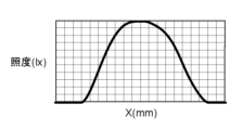
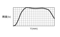
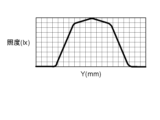
- FIG. 4 is a graph showing the focal length of the Fresnel lens according to the embodiment; 5 is a graph showing the illuminance distribution of the lighting device according to the embodiment; 5 is a graph showing the illuminance distribution of the lighting device according to the embodiment; 5 is a graph showing the illuminance distribution of the lighting device according to the embodiment; 5 is a graph showing the illuminance distribution of the lighting device according to the embodiment; 5 is a graph showing the illuminance distribution of the lighting device according to the embodiment; 5 is a graph showing the illuminance distribution of the lighting device according to the embodiment; The graph which shows the illuminance distribution of the conventional illuminating device. The graph which shows the illuminance distribution of the conventional illuminating device.
- FIG. 4 is a schematic cross-sectional view showing another configuration of the Fresnel lens according to this embodiment;
- Patent Document 1 when the light source is changed from an incandescent lamp to a light emitting diode, the emission intensity changes sharply from on the lens axis to off the lens axis.
- an object of the present disclosure is to provide a lighting device that uses light-emitting diodes as light sources and that suppresses unevenness in the illuminated surface.
- FIG. 1 shows a schematic cross-sectional view of a lighting device according to this embodiment.
- a lighting device 100 in FIG. 1 is, for example, a spotlight used for stage lighting.
- the optical axis direction of the light emitting element 1 is the Z direction
- the vertical direction is the Y direction
- the horizontal direction perpendicular to the Z and Y directions is the X direction.
- the illumination device 100 includes a light emitting element 1, a Fresnel lens 2, a saddle 3, a focus adjustment mechanism 4, and a lamp body 5.
- the light emitting element 1 is a light emitting diode (LED). Since the illumination device 100 is used as a spotlight or the like, a light-emitting diode capable of high output and surface emission is used as the light-emitting element 1 . In this embodiment, a COB (Chip ON board) type LED is used as the light emitting element 1 .
- a COB (Chip ON board) type LED is used as the light emitting element 1 .
- the Fresnel lens 2 is a substantially circular plate-shaped lens that irradiates the light emitted from the light emitting element 1 forward (left side of the drawing in FIG. 1).
- the saddle 3 is a member that holds the light emitting element 1.
- the saddle 3 is attached to the focus adjustment mechanism 4 .
- the focus adjustment mechanism 4 is a mechanism that adjusts the distance L between the light emitting element 1 and the Fresnel lens 2. By operating the focus adjustment mechanism 4, the distance L between the light emitting element 1 and the Fresnel lens 2 can be changed, and the spread angle of the light emitted from the illumination device can be adjusted.
- the lamp body 5 is a hollow cylindrical member that holds the light emitting element 1, the Fresnel lens 2, the saddle 3, and the focus adjustment mechanism 4.
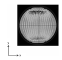
- FIG. 2A and 2B are emission intensity distribution diagrams of the light emitting device according to this embodiment. Specifically, FIG. 2A is a luminous intensity distribution diagram on the light emitting surface of the light emitting element 1, and FIG. 2B is a graph showing the luminous intensity distribution in the X direction and the Y direction of FIG. 2A.
- the emission intensity at the central portion of the light-emitting surface is smaller than the emission intensity at the outer peripheral portion of the light-emitting surface. This difference in emission intensity occurs because, in the COB type LEDs, the LED group in the central portion has higher wiring resistance than the LED group in the outer peripheral portion.
- the luminous intensity at the central portion of the light-emitting surface is higher than the luminous intensity at the outer peripheral portion of the light-emitting surface.
- the emission intensity distribution of the light emitting surface differs between the light emitting diode and the incandescent lamp.
- the light-emitting diode emits less light per unit area than the filament of an incandescent bulb, increasing its area makes the total luminous flux equal to that of the filament. For example, if the filament of the illumination device is 20 mm, the size of the light emitting region of the light emitting diode is 30 mm (10% or more of the lens effective diameter). This point is also different from light emitting diodes and incandescent lamps.
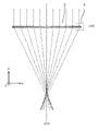
- FIG. 3 is a diagram showing a schematic cross-sectional view of a Fresnel lens according to this embodiment, and FIG. 4 is an enlarged view of region A in FIG.
- the light emitted from the light emitting element 1 is indicated by a dashed line.
- the Fresnel lens 2 includes a base portion 21 and a protruding ring zone portion 22 .
- the ring zone portion 22 is formed along the surface of the base portion 21 .
- the thickness d2 of the base portion 21 is about 4 mm, and the thickness d2 of the annular portion 22 is about 1 mm.
- each annular zone of the Fresnel lens 2 is set by optical design.
- the effective diameter of the lens is 210 mm.
- the lens curvature of the Fresnel lens 2 is set within a movable range of the light emitting element 1 when the focus adjustment mechanism 4 is used, so that the light emitted from the light emitting element 1 can be appropriately irradiated onto the irradiation surface.
- the radius of curvature of the Fresnel lens 2 is set to a value between R100 and 120, and the desired irradiation surface is achieved by setting the conic coefficient to -1.2 ⁇ K ⁇ -0.9. are doing.
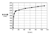
- FIG. 5 is a graph showing the focal length of the Fresnel lens according to this embodiment.
- the Fresnel lens 2 is formed such that the focal length increases from the central portion to the outer peripheral portion.
- the focal length of the Fresnel lens 2 sharply decreases near the center, and increases logarithmically as the X coordinate increases.
- the focal length may increase continuously or stepwise from the central portion of the Fresnel lens 2 to the outer peripheral portion of the Fresnel lens 2 .
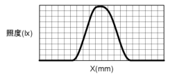
- FIG. 6A to 8B are illuminance distribution diagrams of the illumination device according to this embodiment. Specifically, FIG. 6A shows the illuminance distribution in the X direction when the light is collected (the distance L is large). FIG. 6B shows the illuminance distribution in the Y direction when the light is collected (the distance L is large).
- FIG. 7A shows the illuminance distribution in the X direction at the intermediate time (the distance L is medium).
- FIG. 7B shows the illuminance distribution in the Y direction at the intermediate time (the distance L is medium).
- FIG. 8A shows the illuminance distribution in the X direction during diffusion (distance L is small).
- FIG. 8B shows the illuminance distribution in the Y direction during diffusion (distance L is small).
- 6A to 8B the central portion of the horizontal axis indicates the illuminance at the central portion of the irradiated surface.
- the illuminance gradually changes from the central portion to the outer peripheral portion of the irradiation surface in each state of condensing, intermediate, and diffusing.
- FIGS. 9A and 9B are illuminance distribution diagrams of conventional lighting devices. Specifically, FIGS. 9A and 9B respectively show the illuminance distribution at the intermediate time (the distance L is medium), and FIG. 9A is a graph showing the illuminance distribution in the X direction on the irradiation surface of the conventional lighting device, FIG. 9B is a graph showing the illuminance distribution in the Y direction on the irradiation surface of the conventional lighting device. In FIGS. 9A and 9B, the central portion of the horizontal axis indicates the illuminance at the central portion of the irradiated surface. 9A and 9B, the same light-emitting element (light-emitting diode) as that of the present embodiment is used as the light source of the conventional lighting device.
- the same light-emitting element light-emitting diode
- the emission intensity changes sharply from the lens axis to the lens axis, so unevenness occurs on the illuminated surface.
- the light emitting element 1 in this embodiment is a COB type light emitting diode.
- the emission intensity distribution in the central portion of the light emitting surface is smaller than the emission intensity in the outer peripheral portion (see FIGS. 2A and 2B).
- the light emission intensity of the outer peripheral portion of the light-emitting element 1 is large, when the distribution of each light-emitting surface widens due to lens aberration, the light emission distribution becomes uniform.
- the change in emission intensity from on-axis to off-axis is steeper.
- COB type LEDs are about 1.5 times larger than conventional incandescent light bulbs, the effect of lens aberration is greater for COB type LEDs than for incandescent light bulbs.
- the change in light emission intensity from on the lens axis to off the lens axis becomes steep. It is considered that this causes unevenness in the irradiation surface of the lighting device.
- the spherical aberration of a lens is proportional to the cube of the aperture, and the coma aberration is proportional to the square of the aperture.
- the Fresnel lens 2 is formed so that the focal length increases from the central portion to the outer peripheral portion. That is, the Fresnel lens 2 has aberration. If the Fresnel lens 2 has an aberration, the image of the Fresnel lens 2 will not be perfectly formed and will be out of focus. In other words, the Fresnel lens 2 can suppress the change in illuminance from the outer periphery of the lens to the outside of the lens axis. As a result, it is possible to suppress the occurrence of unevenness on the irradiated surface.
- the Fresnel lens 2 changes the amount of change in focal length with respect to the lens diameter by 10 mm or more per 1 mm in the central portion, and changes by 0.2 mm or less per 1 mm in the outer peripheral portion.
- the amount of change in distance is 50% or more, it is possible to suppress the occurrence of unevenness on the irradiated surface.
- the amount of change in the focal length of the outer peripheral portion of the Fresnel lens 2 with respect to the central portion is 50% or more.
- the luminance of the central portion of the light-emitting element 1 is lower than that of the peripheral portion by 5% or more. For this reason, even if the amount of change in the focal length of the Fresnel lens 2 is changed by about 10 to 20%, it is not possible to suppress the change in the light emission intensity from the outer peripheral portion of the lens to the outside of the lens axis. do. In order to suppress the occurrence of unevenness on the irradiated surface, it is effective to change the amount of change in the focal length as described above.
- the focal length is increased from the central portion to the outer peripheral portion of the Fresnel lens 2 to obtain the above-described effects, but the present invention is not limited to this.
- the Fresnel lens 2 may be configured as shown in FIG. In FIG. 10, the first surface 23, which is the surface of the Fresnel lens 2, may be processed to increase the surface roughness.
- the surface roughness of the first surface 23 is preferably an arithmetic mean roughness Ra of 30 nm to 200 nm. Arithmetic mean roughness Ra of 30 nm or more is preferable because light can be slightly diffused by the first surface 23 .
- setting the arithmetic mean roughness Ra to 200 nm or less is preferable because stable processing and moldability of the Fresnel lens 2 can be achieved.
- the first surface 23 may be processed to increase the surface roughness from the central portion to the outer peripheral portion. By doing so, desired optical characteristics can be realized without greatly impairing the design of the spotlight. As a result, the light emission intensity of the illumination surface of the lighting device 100 becomes moderate from the central portion to the outer peripheral portion, so that the same effects as those of the above embodiment can be obtained.
- the second surface 24 opposite to the first surface 23 may be processed in the same manner as the first surface 23 .
- the lighting device of the present disclosure can be used as a spotlight such as stage lighting.
Landscapes
- Engineering & Computer Science (AREA)
- General Engineering & Computer Science (AREA)
- Non-Portable Lighting Devices Or Systems Thereof (AREA)
Priority Applications (2)
| Application Number | Priority Date | Filing Date | Title |
|---|---|---|---|
| CN202280058420.8A CN117916512A (zh) | 2021-09-02 | 2022-07-15 | 照明装置 |
| JP2023545142A JPWO2023032485A1 (https=) | 2021-09-02 | 2022-07-15 |
Applications Claiming Priority (2)
| Application Number | Priority Date | Filing Date | Title |
|---|---|---|---|
| JP2021-143230 | 2021-09-02 | ||
| JP2021143230 | 2021-09-02 |
Publications (1)
| Publication Number | Publication Date |
|---|---|
| WO2023032485A1 true WO2023032485A1 (ja) | 2023-03-09 |
Family
ID=85412137
Family Applications (1)
| Application Number | Title | Priority Date | Filing Date |
|---|---|---|---|
| PCT/JP2022/027812 Ceased WO2023032485A1 (ja) | 2021-09-02 | 2022-07-15 | 照明装置 |
Country Status (3)
| Country | Link |
|---|---|
| JP (1) | JPWO2023032485A1 (https=) |
| CN (1) | CN117916512A (https=) |
| WO (1) | WO2023032485A1 (https=) |
Citations (3)
| Publication number | Priority date | Publication date | Assignee | Title |
|---|---|---|---|---|
| JP2001307502A (ja) * | 2000-04-25 | 2001-11-02 | R D S Kk | スポットライト及び光源ユニット |
| JP2005259474A (ja) * | 2004-03-10 | 2005-09-22 | Citizen Electronics Co Ltd | 照明装置 |
| JP2009204706A (ja) * | 2008-02-26 | 2009-09-10 | Asahi Rubber Inc | 光透過性光学部品およびその製造方法 |
Family Cites Families (4)
| Publication number | Priority date | Publication date | Assignee | Title |
|---|---|---|---|---|
| JPS63160101A (ja) * | 1986-12-24 | 1988-07-02 | 丸茂電機株式会社 | スポツトライト |
| JP3493630B2 (ja) * | 2001-07-19 | 2004-02-03 | スタンレー電気株式会社 | Led交通信号灯具 |
| JP5481223B2 (ja) * | 2010-02-18 | 2014-04-23 | ミネベア株式会社 | 照明装置、およびレンズシート |
| JP5584858B2 (ja) * | 2012-03-13 | 2014-09-10 | ナルックス株式会社 | 光学装置 |
-
2022
- 2022-07-15 WO PCT/JP2022/027812 patent/WO2023032485A1/ja not_active Ceased
- 2022-07-15 JP JP2023545142A patent/JPWO2023032485A1/ja active Pending
- 2022-07-15 CN CN202280058420.8A patent/CN117916512A/zh active Pending
Patent Citations (3)
| Publication number | Priority date | Publication date | Assignee | Title |
|---|---|---|---|---|
| JP2001307502A (ja) * | 2000-04-25 | 2001-11-02 | R D S Kk | スポットライト及び光源ユニット |
| JP2005259474A (ja) * | 2004-03-10 | 2005-09-22 | Citizen Electronics Co Ltd | 照明装置 |
| JP2009204706A (ja) * | 2008-02-26 | 2009-09-10 | Asahi Rubber Inc | 光透過性光学部品およびその製造方法 |
Also Published As
| Publication number | Publication date |
|---|---|
| JPWO2023032485A1 (https=) | 2023-03-09 |
| CN117916512A (zh) | 2024-04-19 |
Similar Documents
| Publication | Publication Date | Title |
|---|---|---|
| JP4755276B2 (ja) | 照明用光源 | |
| JP5363864B2 (ja) | 発光装置および電球型ledランプ | |
| KR101194703B1 (ko) | 적어도 하나의 발광 소자를 구비한 광원 및 조명 장치 | |
| KR101948378B1 (ko) | 발광 다이오드용 절두원추형 표면을 포함한 전방향 반사기 | |
| US8106568B2 (en) | Lighting device capable of suppressing occurrence of ovelap of multiple shades | |
| JP2014524105A (ja) | Led用の光学レンズに関連する方法及び装置 | |
| CN103982838A (zh) | 照明器具 | |
| JP5292790B2 (ja) | 照明装置 | |
| US20130163239A1 (en) | Mixing optical zoom system with moving gate and gobo | |
| JP2015072838A (ja) | 発光モジュール、照明用光源及び照明装置 | |
| JP6156791B2 (ja) | 照明器具 | |
| CN106662295B (zh) | 具有虚拟光源的照明装置 | |
| JP5547697B2 (ja) | 発光装置および照明装置 | |
| US9371975B2 (en) | Light source device | |
| CN204459822U (zh) | 照明装置 | |
| CN204141300U (zh) | 照明装置 | |
| WO2023032485A1 (ja) | 照明装置 | |
| JP2014102973A (ja) | 照明装置 | |
| AU2011282009B2 (en) | Torch with a rotationally symmetrical optical attachment | |
| JP2014182995A (ja) | 照明装置 | |
| JP5820365B2 (ja) | 発光装置および光照射装置 | |
| KR101191406B1 (ko) | 백열등의 배광 패턴을 갖는 led 등기구 | |
| CN220338298U (zh) | 照明装置 | |
| CN110671677A (zh) | 手术用照明系统 | |
| KR20190049457A (ko) | Led램프 및 이를 구비하는 조명 장치 |
Legal Events
| Date | Code | Title | Description |
|---|---|---|---|
| 121 | Ep: the epo has been informed by wipo that ep was designated in this application |
Ref document number: 22864073 Country of ref document: EP Kind code of ref document: A1 |
|
| WWE | Wipo information: entry into national phase |
Ref document number: 2023545142 Country of ref document: JP |
|
| WWE | Wipo information: entry into national phase |
Ref document number: 202280058420.8 Country of ref document: CN |
|
| NENP | Non-entry into the national phase |
Ref country code: DE |
|
| 122 | Ep: pct application non-entry in european phase |
Ref document number: 22864073 Country of ref document: EP Kind code of ref document: A1 |