WO2023032005A1 - 光測定装置 - Google Patents
光測定装置 Download PDFInfo
- Publication number
- WO2023032005A1 WO2023032005A1 PCT/JP2021/031748 JP2021031748W WO2023032005A1 WO 2023032005 A1 WO2023032005 A1 WO 2023032005A1 JP 2021031748 W JP2021031748 W JP 2021031748W WO 2023032005 A1 WO2023032005 A1 WO 2023032005A1
- Authority
- WO
- WIPO (PCT)
- Prior art keywords
- light
- interference
- measurement
- unit
- optical path
- Prior art date
- Legal status (The legal status is an assumption and is not a legal conclusion. Google has not performed a legal analysis and makes no representation as to the accuracy of the status listed.)
- Ceased
Links
Images





Classifications
-
- G—PHYSICS
- G01—MEASURING; TESTING
- G01B—MEASURING LENGTH, THICKNESS OR SIMILAR LINEAR DIMENSIONS; MEASURING ANGLES; MEASURING AREAS; MEASURING IRREGULARITIES OF SURFACES OR CONTOURS
- G01B9/00—Measuring instruments characterised by the use of optical techniques
- G01B9/02—Interferometers
- G01B9/02001—Interferometers characterised by controlling or generating intrinsic radiation properties
- G01B9/02002—Interferometers characterised by controlling or generating intrinsic radiation properties using two or more frequencies
- G01B9/02004—Interferometers characterised by controlling or generating intrinsic radiation properties using two or more frequencies using frequency scans
-
- G—PHYSICS
- G01—MEASURING; TESTING
- G01B—MEASURING LENGTH, THICKNESS OR SIMILAR LINEAR DIMENSIONS; MEASURING ANGLES; MEASURING AREAS; MEASURING IRREGULARITIES OF SURFACES OR CONTOURS
- G01B9/00—Measuring instruments characterised by the use of optical techniques
- G01B9/02—Interferometers
- G01B9/02055—Reduction or prevention of errors; Testing; Calibration
- G01B9/02075—Reduction or prevention of errors; Testing; Calibration of particular errors
-
- G—PHYSICS
- G01—MEASURING; TESTING
- G01B—MEASURING LENGTH, THICKNESS OR SIMILAR LINEAR DIMENSIONS; MEASURING ANGLES; MEASURING AREAS; MEASURING IRREGULARITIES OF SURFACES OR CONTOURS
- G01B9/00—Measuring instruments characterised by the use of optical techniques
- G01B9/02—Interferometers
-
- A—HUMAN NECESSITIES
- A61—MEDICAL OR VETERINARY SCIENCE; HYGIENE
- A61B—DIAGNOSIS; SURGERY; IDENTIFICATION
- A61B5/00—Measuring for diagnostic purposes; Identification of persons
- A61B5/0059—Measuring for diagnostic purposes; Identification of persons using light, e.g. diagnosis by transillumination, diascopy, fluorescence
- A61B5/0062—Arrangements for scanning
- A61B5/0066—Optical coherence imaging
-
- A—HUMAN NECESSITIES
- A61—MEDICAL OR VETERINARY SCIENCE; HYGIENE
- A61B—DIAGNOSIS; SURGERY; IDENTIFICATION
- A61B5/00—Measuring for diagnostic purposes; Identification of persons
- A61B5/72—Signal processing specially adapted for physiological signals or for diagnostic purposes
- A61B5/7235—Details of waveform analysis
- A61B5/7253—Details of waveform analysis characterised by using transforms
- A61B5/7257—Details of waveform analysis characterised by using transforms using Fourier transforms
-
- G—PHYSICS
- G01—MEASURING; TESTING
- G01B—MEASURING LENGTH, THICKNESS OR SIMILAR LINEAR DIMENSIONS; MEASURING ANGLES; MEASURING AREAS; MEASURING IRREGULARITIES OF SURFACES OR CONTOURS
- G01B11/00—Measuring arrangements characterised by the use of optical techniques
-
- G—PHYSICS
- G01—MEASURING; TESTING
- G01B—MEASURING LENGTH, THICKNESS OR SIMILAR LINEAR DIMENSIONS; MEASURING ANGLES; MEASURING AREAS; MEASURING IRREGULARITIES OF SURFACES OR CONTOURS
- G01B11/00—Measuring arrangements characterised by the use of optical techniques
- G01B11/02—Measuring arrangements characterised by the use of optical techniques for measuring length, width or thickness
- G01B11/026—Measuring arrangements characterised by the use of optical techniques for measuring length, width or thickness by measuring distance between sensor and object
-
- G—PHYSICS
- G01—MEASURING; TESTING
- G01B—MEASURING LENGTH, THICKNESS OR SIMILAR LINEAR DIMENSIONS; MEASURING ANGLES; MEASURING AREAS; MEASURING IRREGULARITIES OF SURFACES OR CONTOURS
- G01B9/00—Measuring instruments characterised by the use of optical techniques
- G01B9/02—Interferometers
- G01B9/02055—Reduction or prevention of errors; Testing; Calibration
- G01B9/02062—Active error reduction, i.e. varying with time
- G01B9/02064—Active error reduction, i.e. varying with time by particular adjustment of coherence gate, i.e. adjusting position of zero path difference in low coherence interferometry
-
- G—PHYSICS
- G01—MEASURING; TESTING
- G01B—MEASURING LENGTH, THICKNESS OR SIMILAR LINEAR DIMENSIONS; MEASURING ANGLES; MEASURING AREAS; MEASURING IRREGULARITIES OF SURFACES OR CONTOURS
- G01B9/00—Measuring instruments characterised by the use of optical techniques
- G01B9/02—Interferometers
- G01B9/02055—Reduction or prevention of errors; Testing; Calibration
- G01B9/0207—Error reduction by correction of the measurement signal based on independently determined error sources, e.g. using a reference interferometer
-
- G—PHYSICS
- G01—MEASURING; TESTING
- G01B—MEASURING LENGTH, THICKNESS OR SIMILAR LINEAR DIMENSIONS; MEASURING ANGLES; MEASURING AREAS; MEASURING IRREGULARITIES OF SURFACES OR CONTOURS
- G01B9/00—Measuring instruments characterised by the use of optical techniques
- G01B9/02—Interferometers
- G01B9/02055—Reduction or prevention of errors; Testing; Calibration
- G01B9/02075—Reduction or prevention of errors; Testing; Calibration of particular errors
- G01B9/02078—Caused by ambiguity
-
- G—PHYSICS
- G01—MEASURING; TESTING
- G01B—MEASURING LENGTH, THICKNESS OR SIMILAR LINEAR DIMENSIONS; MEASURING ANGLES; MEASURING AREAS; MEASURING IRREGULARITIES OF SURFACES OR CONTOURS
- G01B9/00—Measuring instruments characterised by the use of optical techniques
- G01B9/02—Interferometers
- G01B9/02083—Interferometers characterised by particular signal processing and presentation
- G01B9/02085—Combining two or more images of different regions
-
- G—PHYSICS
- G01—MEASURING; TESTING
- G01B—MEASURING LENGTH, THICKNESS OR SIMILAR LINEAR DIMENSIONS; MEASURING ANGLES; MEASURING AREAS; MEASURING IRREGULARITIES OF SURFACES OR CONTOURS
- G01B9/00—Measuring instruments characterised by the use of optical techniques
- G01B9/02—Interferometers
- G01B9/0209—Low-coherence interferometers
- G01B9/02091—Tomographic interferometers, e.g. based on optical coherence
-
- G—PHYSICS
- G01—MEASURING; TESTING
- G01J—MEASUREMENT OF INTENSITY, VELOCITY, SPECTRAL CONTENT, POLARISATION, PHASE OR PULSE CHARACTERISTICS OF INFRARED, VISIBLE OR ULTRAVIOLET LIGHT; COLORIMETRY; RADIATION PYROMETRY
- G01J1/00—Photometry, e.g. photographic exposure meter
- G01J1/02—Details
- G01J1/04—Optical or mechanical part supplementary adjustable parts
- G01J1/0407—Optical elements not provided otherwise, e.g. manifolds, windows, holograms, gratings
-
- G—PHYSICS
- G01—MEASURING; TESTING
- G01J—MEASUREMENT OF INTENSITY, VELOCITY, SPECTRAL CONTENT, POLARISATION, PHASE OR PULSE CHARACTERISTICS OF INFRARED, VISIBLE OR ULTRAVIOLET LIGHT; COLORIMETRY; RADIATION PYROMETRY
- G01J1/00—Photometry, e.g. photographic exposure meter
- G01J1/02—Details
- G01J1/04—Optical or mechanical part supplementary adjustable parts
- G01J1/0407—Optical elements not provided otherwise, e.g. manifolds, windows, holograms, gratings
- G01J1/0422—Optical elements not provided otherwise, e.g. manifolds, windows, holograms, gratings using light concentrators, collectors or condensers
-
- G—PHYSICS
- G01—MEASURING; TESTING
- G01N—INVESTIGATING OR ANALYSING MATERIALS BY DETERMINING THEIR CHEMICAL OR PHYSICAL PROPERTIES
- G01N21/00—Investigating or analysing materials by the use of optical means, i.e. using sub-millimetre waves, infrared, visible or ultraviolet light
- G01N21/17—Systems in which incident light is modified in accordance with the properties of the material investigated
-
- G—PHYSICS
- G01—MEASURING; TESTING
- G01N—INVESTIGATING OR ANALYSING MATERIALS BY DETERMINING THEIR CHEMICAL OR PHYSICAL PROPERTIES
- G01N21/00—Investigating or analysing materials by the use of optical means, i.e. using sub-millimetre waves, infrared, visible or ultraviolet light
- G01N21/17—Systems in which incident light is modified in accordance with the properties of the material investigated
- G01N21/47—Scattering, i.e. diffuse reflection
- G01N21/4795—Scattering, i.e. diffuse reflection spatially resolved investigating of object in scattering medium
-
- G—PHYSICS
- G01—MEASURING; TESTING
- G01B—MEASURING LENGTH, THICKNESS OR SIMILAR LINEAR DIMENSIONS; MEASURING ANGLES; MEASURING AREAS; MEASURING IRREGULARITIES OF SURFACES OR CONTOURS
- G01B2290/00—Aspects of interferometers not specifically covered by any group under G01B9/02
- G01B2290/35—Mechanical variable delay line
-
- G—PHYSICS
- G01—MEASURING; TESTING
- G01B—MEASURING LENGTH, THICKNESS OR SIMILAR LINEAR DIMENSIONS; MEASURING ANGLES; MEASURING AREAS; MEASURING IRREGULARITIES OF SURFACES OR CONTOURS
- G01B2290/00—Aspects of interferometers not specifically covered by any group under G01B9/02
- G01B2290/70—Using polarization in the interferometer
Definitions
- This disclosure relates to optical measurement technology.
- optical ranging technology that uses the interference phenomenon of light.
- the light emitted from the light source is split into the reference light and the measurement light, and the reference light and the reflected light, which is the light that the measurement light is reflected on the object, are split. Interference is allowed and the distance from the light source to the object is measured based on the constructive condition of the reference light and the reflected light.
- a tomometer to which such an optical ranging technique is applied is known as an optical coherence tomography (OCT).
- optical ranging techniques include wavelength scanning interferometry and white light interferometry.
- the wavelength scanning interference method light emitted from a light source is wavelength-swept, and the wavelength-swept light is split into measurement light and reference light. The measurement light is reflected on the object to become reflected light, and the reflected light and the reference light interfere with each other to generate interference light. By measuring the frequency of the interfering light, the distance from the light source to the object is determined.
- An optical coherence tomography to which the wavelength scanning interferometry method is applied is known as a wavelength sweeping optical coherence tomography (SS-OCT: Swept Source-OCT).
- the white light interference method is also called the spectral domain interference method, and uses a white light source that emits broadband light.
- the white interference method splits broadband light emitted from a light source into measurement light and reference light.
- the measurement light is reflected on the object to become reflected light, and the reflected light and the reference light interfere with each other to generate interference light.
- the distance from the light source to the object is measured by spatially spectrally spectroscopy the interference light with a spectroscope and Fourier transforming the interference fringes generated based on the interference conditions.
- Optical coherence tomography to which the white interference method is applied is known as spectral domain type optical coherence tomography (SD-OCT).
- SD-OCT spectral domain type optical coherence tomography
- Both of these methods utilize the fact that optical interference is detected when the optical path length difference between the measurement light and the reference light is within the range of the coherence length of the light source.
- the coherence length which determines the measurable range in a single measurement, varies depending on the specifications of the light source and is inversely proportional to the line width of the light source. In other words, the narrower the linewidth, the longer the coherence length, and the wider the measurable range in a single measurement. However, in general, the narrower the linewidth, the higher the cost. In order to have it, ingenuity is required.
- Patent Document 1 discloses a technique for substantially expanding the measurement range by providing a mechanism for adjusting the delay length of the reference light using a movable mirror and repeating the measurement while changing the optical path length of the reference light. ing.
- the optical path length of the reference light is adjusted so that the optical path length of the reflected light and the optical path length of the reference light are the same, and the reflected light and the reference light are combined.
- a low-cost light source with a short coherence length can be used to expand the substantial measurable range.
- the present disclosure has been made to solve such problems, and aims to provide an optical measurement technique capable of distance measurement while suppressing the influence of optical path length fluctuations due to environmental temperature.
- a light identification device includes a branching unit that branches light emitted from a laser light source into a measurement light and a reference light, and a first interference light that is obtained by interfering two orthogonal polarized waves of the reference light, A second interference light obtained by interfering two orthogonal polarized waves of the reflected light of the measurement light from the object, and a third interference light obtained by interfering the reference light and the reflected light.
- a switching interference unit for outputting a state in which the polarization states are separated; a photoelectric conversion unit for receiving each interference light and converting the received interference light into an electric signal; a digital conversion unit that outputs a subsequent digital signal as a received signal, and converts the received signal into a frequency spectrum to determine an optical path length difference between the two orthogonal polarized waves of the reference light and between the two orthogonal polarized waves of the reflected light.
- a calculation processing unit that obtains an optical path length difference and an optical path length difference between the reference light and the measurement light.
- distance measurement can be performed while suppressing the effects of optical path length fluctuations due to environmental temperature.
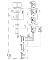
- FIG. 1 is a block diagram showing a configuration example of a light measurement device according to Embodiment 1.
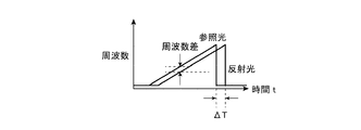
- FIG. 2A is a diagram showing an example of the relationship between reference light and reflected light input to a switching interference unit when a distance between a transmitting unit and an object is a specific distance according to Embodiment 1.
- FIG. 2B is a diagram showing an example of a temporal waveform of interference light intensity obtained from the reference light and reflected light shown in FIG. 2A.
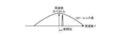
- FIG. 2C is a diagram showing an example of the frequency spectrum output from the calculation processing unit based on the time waveform of the interference light intensity at a certain time.
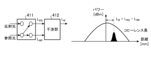
- 3A and 3B are diagrams for explaining the switching unit and the interference unit of the optical measurement device according to the first embodiment.
- FIG. 3A is a diagram showing a form for measuring temperature variation of reference light.
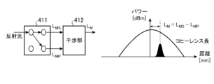
- 3A and 3B are diagrams for explaining the switching unit and the interference unit of the optical measurement device according to the first embodiment.
- FIG. 3B is a diagram showing a form for measuring temperature variation of reflected light.
- 3A and 3B are diagrams for explaining the switching unit and the interference unit of the optical measurement device according to the first embodiment.
- FIG. 3C is a diagram showing a form in the case of performing distance measurement to an object from multiplexing of the same polarized waves of the reference light and the measurement light.
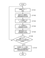
- FIG. 4 is a flowchart for explaining the operation of the light measurement device according to Embodiment 1.
- FIG. 5 is a block diagram showing a configuration example of a light measuring device according to the second embodiment.
- 6A and 6B are diagrams for explaining the switching unit and the interference unit of the optical measurement device according to the second embodiment.
- FIG. 7 is a block diagram showing a configuration example of a light measuring device according to Embodiment 3. As shown in FIG.
- the optical measurement apparatus includes a transmitter 10, a switching interference unit 41, a switching controller 42, a receiver 20, and a calculation processor 30.
- the transmitter 10 includes a laser light source 11 , a sweeper 12 , a splitter 13 , an optical circulator 14 and an irradiation system 15 .
- the receiver 20 includes a photoelectric converter 21 and a digital converter 22 .
- the laser light source 11 emits continuous laser light.
- the laser light source 11 is, for example, a semiconductor laser, and emits laser light with a predetermined frequency.
- the sweep unit 12 sweeps the wavelength of the laser light emitted by the laser light source 11 .
- the sweeping unit 12 outputs the laser light after the sweep as the sweeping light.
- the sweep light output from the sweep unit 12 is continuous wave laser light.
- the splitter 13 is composed of an optical coupler or the like, and splits the input light at a predetermined power ratio.
- the splitter 13 splits the sweep light output from the sweeper at a predetermined power ratio, and outputs the split laser light as the measurement light and the reference light.
- the measurement light is guided to the optical circulator 14 and the reference light is guided to the switching interference section 41 .
- the optical circulator 14 is composed of, for example, a 3-port optical circulator and guides the measurement light to the irradiation system 15 . Also, the optical circulator 14 guides the reflected light, which is the light reflected on the object from the irradiated measurement light, to the switching interference section 41 .
- the irradiation system 15 irradiates the object with the measurement light.
- the irradiation system 15 includes a connector 151 for connecting optical fibers, and a lens 152 such as one or more transmissive lenses or one or more reflective lenses. After the measurement light guided to is collimated and condensed, an object is irradiated with the condensed measurement light. Alternatively, without using the lens 152, the measurement light may be directly irradiated onto the object from the end of the connector 151. FIG. Also, the irradiation system 15 guides the reflected light to the optical circulator 14 .
- switching interference unit switching control unit
- the reference light and the reflected light are input to the switching interference unit 41, and the switching interference unit 41 causes the first interference light obtained by causing the two orthogonal polarized waves of the reference light to interfere with each other, and the two orthogonal polarized waves of the reflected light to interfere with each other.
- second interfering light or third interfering light obtained by interfering the reference light and the reflected light.
- the switching interference section 41 includes a switching section 411 and an interference section 412 as shown in FIGS. 3A to 3C.
- the switching unit 411 sequentially switches the optical path to any one of a pattern of two orthogonal polarized waves of the reference light, a pattern of two orthogonal polarized waves of the reflected light, and a pattern of the reference light and the reflected light.
- the two polarized waves or the reference light and the reflected light in the pattern are output to the interference section 412 .
- Switching of the optical path is performed using an optical switch and a VOA (Variable Optical Attenuator) based on a signal from the switching control unit 42 . Since the switching of the optical path is performed for each sweep of the sweeping section 12 , the time for switching the path in the switching control section 42 is controlled by the electric signal from the sweeping section 12 .
- VOA Very Optical Attenuator
- the frequency ratio of switching may be equal or unequal among the patterns. For example, when the intensity of the reflected light from the object is low, the frequency ratio of switching to the path of the pattern that causes the two orthogonal polarized waves of the reference light to interfere is adapted according to the intensity of the reflected light in order to obtain more of the reflected light from the object. can be lowered.
- the interference unit 412 is composed of, for example, a fiber coupler, and causes the input light to interfere.
- the interference unit 412 interferes the two orthogonal polarized waves of the reference light, the two orthogonal polarized waves of the reflected light, or the reference light and the reflected light of the same polarized wave. Further, the interference unit 412 outputs the interference light obtained by interfering the two orthogonal polarized waves of the reference light or the two orthogonal polarized waves of the reflected light in a state in which the orthogonal polarization states of the respective interference lights are separated. . Further, the interference unit 412 outputs interference light after causing the reference light and the reflected light of the same polarization to interfere with each other.
- each interference light can be obtained substantially at the same time.
- a member capable of separating two orthogonal polarized waves is used for the interference unit 412 .
- ICR Intradyne Coherent Receiver
- two orthogonal polarized waves can be separated. Further details of the switching interference unit 41 will be described later.
- the photoelectric conversion section 21 photoelectrically converts the interference light output from the switching interference section 41 and outputs an analog signal representing the interference light.
- the digital converter 22 A/D converts the analog signal and outputs the digital signal after A/D conversion as a received signal.
- the photoelectric conversion section 21 and the digital conversion section 22 constitute a receiving section. That is, the receiver receives the reference light and the reflected light, which is the light reflected by the object, and outputs a received signal indicating interference light.
- the calculation processing unit 30 outputs the measured distance from the frequency spectrum of the interference light based on the received signal. More specifically, for example, the calculation processing unit 30 measures the frequency spectrum of the interference light by Fourier transforming the received signal. The measurement distance is determined by the optical path length difference between the measurement light and the reference light. The frequency obtained when the optical path length difference between the two from the branching portion 13 is 0 is 0, and the frequency increases in proportion to the optical path length difference. By measuring this value, the distance of the object to be measured is measured. At this time, the distance at which the frequency spectrum can be obtained is limited by the coherence length.
- the optical circulator 14 and the connector 151, and the optical circulator 14 and the switching interference unit 41 are connected by optical fibers, for example, and the laser light is guided through the optical fibers.
- the path along which light propagates from the branching portion 13 to the photoelectric conversion portion 21 is composed of a polarization-maintaining fiber that maintains two orthogonal polarization states, such as a polarization-maintaining fiber.
- a path and a path between the optical circulator 14 and the switching interference unit 41 are constructed of a polarization maintaining fiber.
- All or part of the switching control unit 42 and the calculation processing unit 30 are implemented, for example, by a computer equipped with a processor and memory (not shown). These functional units are realized by reading out and executing programs stored in the memory by the processor. Programs may be implemented as software, firmware, or a combination of software and firmware. Examples of memory include non-volatile or volatile semiconductor memories such as RAM (Random Access Memory), ROM (Read Only Memory), flash memory, EPROM (Erasable Programmable Read Only Memory), EEPROM (Electrically-EPROM) , magnetic discs, flexible discs, optical discs, compact discs, mini discs, and DVDs.
- RAM Random Access Memory
- ROM Read Only Memory
- flash memory EPROM (Erasable Programmable Read Only Memory)
- EEPROM Electrically-EPROM
- all or part of the switching control unit 42 and the calculation processing unit 30 may be realized by a processing circuit (not shown) instead of the processor and memory.
- the processing circuit is, for example, a single circuit, a composite circuit, a programmed processor, a parallel programmed processor, an ASIC (Application Specific Integrated Circuit), an FPGA (Field-Programmable Gate Array), or a combination thereof. .
- FIG. 2A is an example of the time-frequency relationship between the reference light and the reflected light
- FIG. 2B is an example of the intensity graph of the interference light versus time
- FIG. 2C is an example of the frequency spectrum after Fourier transform of the interference light. showing.
- the reflected light is delayed with respect to the reference light according to the distance to the object. Therefore, in FIG. 2A, the reflected light is shown shifted to the right by the time ⁇ T with respect to the reference light. When the object is far away, the time ⁇ T increases, and the frequency difference also increases in proportion to the time. If the path length of the reference light is set longer than the path length of the reflected light, the reference light is delayed with respect to the reflected light.
- FIG. 2B shows the intensity signal with respect to time of the interference light obtained by combining the reference light and the reflected light shifted by time ⁇ T in the interference section 412 .
- the calculation processing unit 30 has a frequency measurement function, and the calculation processing unit 30 measures the intensity (frequency spectrum) of each frequency component of the interference light based on the interference light.
- FIG. 2C is a diagram showing the frequency spectrum of the interference light measured by the frequency measuring unit based on the interference light shown in FIG. 2B.
- the horizontal axis indicates the frequency
- the vertical axis indicates the intensity of the interference light.
- the intensity of the frequency spectrum decreases as the distance difference between the reference light and the reflected light increases.
- the value of the distance difference when the intensity drops by 3 dB from the maximum value (when the intensity becomes 1/2) is defined as the coherence length, which is expressed by the following equation (1).
- c is the speed of light
- ⁇ is the line width of the light source.
- the coherence length is inversely proportional to the linewidth of the source.
- the coherence length of a laser source is inversely proportional to cost, with narrower linewidth laser sources costing more.
- the coherence length of low-cost laser sources is limited to less than a few tens of millimeters.
- FIG. 3A shows an example of the path and frequency spectrum of the switching unit 411 when measuring the optical path length difference between the two orthogonal polarized waves of the reference light
- FIG. 3B shows an example of the optical path length difference between the two orthogonal polarized waves of the reflected light
- FIG. 3C shows the switching unit 411 and an example of the frequency spectrum when the distance to the object is measured from the optical path length difference between the reference light and the reflected light, and the example of the frequency spectrum. Only one of the two orthogonal polarization states is used when measuring the distance to an object.
- the optical path length is expressed as the product of the refractive index and length.
- a measurement method using an interference system according to the present disclosure performs distance measurement by measuring the optical path length difference between two paths of reference light and reflected light.
- the refractive index and the glass length of the material have temperature dependence, so the optical path length changes according to changes in the environmental temperature. Let this proportional coefficient be a coefficient of linear expansion ⁇ .
- the cross section of the optical fiber core which is the propagation path
- the cross section of the optical fiber core which is the propagation path
- the optical path length is also different between the two polarization states accordingly.
- This refractive index difference is called birefringence.
- the birefringence is unevenly distributed in the longitudinal direction, and the polarization state fluctuates with time due to temperature distribution or stress caused by twisting.
- an optical fiber that incorporates birefringence into its design is called a polarization-maintaining fiber.
- This is designed to prevent polarization crosstalk during transmission by incorporating rods parallel to the core in the longitudinal direction of the optical fiber in order to maintain the polarization state. Therefore, the birefringence in the longitudinal direction is uniform, and the temperature dependence of the birefringence also has a linear relationship. Let ⁇ be this proportional coefficient.
- the optical path lengths of the two orthogonal polarization states of the reference light from the splitter 13 to the interference unit 412 are L RS and L RP .
- ⁇ TR be the amount of temperature change (temperature difference) from the reference temperature of the path of the reference light.
- L RO be the path length of the reference light at a reference temperature (for example, 25° C.) obtained in advance. Then, the optical path length difference L R between the two orthogonal polarization states is represented by the following equation (2).
- the optical path lengths of the two orthogonal polarization states of the reflected light from the splitter 13 to the interference unit 412 be L MS and L MP .
- ⁇ TM be the amount of temperature change (temperature difference) from the reference temperature on the path of the reflected light.
- LMO the reflected light path length at the previously obtained reference temperature.
- the optical path length difference LM between the two orthogonal polarization states is represented by the following equation (4).
- equation (5) is obtained that expresses the correlation between the optical path difference L M and the temperature difference ⁇ T M.
- L the optical path length difference between the reference light and the reflected light.
- the value of L changes under the influence of temperature changes in both paths. Therefore, the temperature term is eliminated using the above equations (3) and (5).
- Equation (7) indicates the optical path length difference to the object at the reference temperature. Therefore, by obtaining in advance the length of each path at the reference temperature, the linear expansion coefficient ⁇ of the polarization-maintaining fiber, and the temperature coefficient ⁇ of the birefringence, the values L, ⁇ L R , and ⁇ L From M , it is possible to perform distance measurement while suppressing the influence of temperature change. At this time, the polarization states of the reflected light and the reference light are matched.
- step ST101 the switching control section 42 determines the pattern of the switching section 411 according to the path to be subjected to temperature correction. Specifically, as shown in FIGS. 3A to 3C, any one of a pattern of two orthogonal polarized waves of the reference light, a pattern of two orthogonal polarized waves of the reflected light, or a pattern of the reference light and the reflected light. First, the pattern of the switching unit 411 is determined.
- the calculation processing section 30 obtains the optical path length difference of the two orthogonal polarized lights. Since the difference frequency of the two orthogonally polarized waves is proportional to the optical path length, the optical path length difference can be obtained from the peak position of the spectrum obtained by Fourier transform.
- step ST102 the calculation processing unit 30 obtains a difference frequency signal of two orthogonal polarizations as shown in FIG. 2B.
- step ST103 the calculation processing section 30 Fourier-transforms the difference frequency signal to obtain a frequency spectrum.
- step ST104 the calculation processing section 30 obtains the optical path length difference from the frequency spectrum.
- step ST105 the calculation processing section 30 acquires the optical path length difference from the reference temperature. Since the optical path difference obtained from the frequency spectrum depends on temperature according to equation (3) or (5), the optical path difference from the reference temperature is obtained according to equation (3) or (5).
- step ST106 the calculation processing section 30 determines whether or not the optical path length difference from the reference temperature has been acquired for all switching patterns. If not acquired, the process returns to step ST101. If acquired, the process proceeds to step ST107.
- step ST107 the calculation processing unit 30 obtains the difference frequency between the reference light and the reflected light obtained by each switching pattern, thereby measuring the distance to the object.
- the obtained values are corrected using equations (3) and (5). This corresponds to equation (7).
- the ratio of the switching frequencies of the three patterns shown in FIGS. 3A to 3C may be evenly 1:1:1, or may be uneven. For example, for a reflection from an object whose frequency spectrum intensity is unknown, the ratio of switching frequencies of the three patterns is not uniform so that a sufficient number of times of averaging can be obtained by obtaining the reflected light multiple times. may Alternatively, the switching control unit 42 may adaptively change the ratio according to the intensity of the frequency spectrum.
- the spectrum intensity after combining is the highest at 1:1 on each axis. However, it can vary greatly depending on the polarization ratio in air and on the surface of the object. Therefore, a polarization controller may be introduced downstream of the optical circulator 14 to adaptively change the polarization ratio. Similarly, the branching ratio in the branching section 13 may be adaptively changed according to the extinction ratio on the surface of the object.
- the polarization intensity of either of the two orthogonal polarized waves must not be 0.
- the polarization intensity can fluctuate during the measurement due to fiber wobble or polarization rotation at the target. Therefore, the polarization intensity ratio in the laser light source 11 may be adaptively changed by feeding back the polarization intensity ratio variation obtained by the photoelectric section.
- Embodiment 2 A light measuring device according to a second embodiment will be described with reference to FIGS. 5 and 6.
- FIG. 5 the optical measurement device according to the second embodiment includes a transmitter 10A, a switching interference unit 41A, a switching controller 42, a receiver 20, and a calculation processor 30.
- FIG. The transmitter 10 includes a laser light source 11 , a sweeper 12 , a splitter 13A, an optical circulator 14 and an irradiation system 15 .
- the light measuring device is provided with a plurality of reference light paths (reference light paths) from the branching section 13A to the switching interference section 41A.
- the path lengths of the plurality of reference beams are different from each other. If there are only two switching paths, two reflected lights to be distance-measured must exist within the coherence length.
- a plurality of reference light paths from the branching unit 13 to the switching interference unit 41A as shown in FIG. 5, such a need is eliminated. That is, by providing a plurality of reference light paths having different lengths, the reference light can be delayed with respect to the reflected light in multiple stages, so that the measurable range can be expanded.
- the optical path lengths of the plurality of reference beams be L Rk (k is an integer from 1 to 4).
- the measurement range is defined by the coherence length centered at the point where the optical path lengths of the reference and reflected light are equal (see FIG. 2C). Therefore, the measurement range can be expanded by using a plurality of reference light paths and switching the measurement path with the switching unit 41A1. At this time, it is assumed that each difference is sufficiently shorter than the coherence length.
- Embodiment 3 A light measuring device according to Embodiment 3 will be described with reference to FIG.
- FIG. 7 shows an optical measurement device according to SD-OCT technology.
- the optical measurement device includes a transmission section 10B, a switching interference section 41B, a switching control section 42B, a reception section 20, and a calculation processing section 30.
- the transmitter 10B includes a white light source 11B, a splitter 13, an optical circulator 14, and an illumination system 15.
- the light measuring device uses a white light source 11B, which is a white laser light source. Therefore, the optical measurement device according to the third embodiment does not require the sweeping section 12 that sweeps the wavelength used in the first embodiment. Since wavelength sweeping is not performed in the optical measurement apparatus according to Embodiment 3, the switching control section 42B controls the switching section (not shown) of the switching interference section 41B based on preset timing.
- the white light source 11B may be used instead of sweeping the wavelength.
- a device such as a diffraction grating that generates spectral light according to the wavelength is provided after the interference section, and interference light is transmitted through such a device to obtain transmitted light. Then, by irradiating a two-dimensional photoelectric conversion device (photoelectric conversion unit 21) such as CMOS with the transmitted light, spectral intensity can be obtained in an analog manner.
- the optical measurement device of the present disclosure can be used as a measurement device for measuring various parts.
- 10 (10A; 10B) transmitting section, 11 laser light source, 11B white light source (white laser light source), 12 sweeping section, 13 (13A) branching section, 14 optical circulator, 15 irradiation system, 20 receiving section, 21 photoelectric conversion section, 22 Digital conversion unit, 30 calculation processing unit, 41 (41A; 41B) switching interference unit, 41A1 switching unit, 42 (42B) switching control unit, 151 connector, 152 lens, 411 switching unit, 412 interference unit.
Landscapes
- Physics & Mathematics (AREA)
- General Physics & Mathematics (AREA)
- Health & Medical Sciences (AREA)
- Life Sciences & Earth Sciences (AREA)
- General Health & Medical Sciences (AREA)
- Pathology (AREA)
- Engineering & Computer Science (AREA)
- Chemical & Material Sciences (AREA)
- Analytical Chemistry (AREA)
- Biochemistry (AREA)
- Immunology (AREA)
- Biophysics (AREA)
- Animal Behavior & Ethology (AREA)
- Radiology & Medical Imaging (AREA)
- Spectroscopy & Molecular Physics (AREA)
- Veterinary Medicine (AREA)
- Signal Processing (AREA)
- Biomedical Technology (AREA)
- Heart & Thoracic Surgery (AREA)
- Medical Informatics (AREA)
- Molecular Biology (AREA)
- Surgery (AREA)
- Nuclear Medicine, Radiotherapy & Molecular Imaging (AREA)
- Public Health (AREA)
- Optics & Photonics (AREA)
- Mathematical Physics (AREA)
- Artificial Intelligence (AREA)
- Computer Vision & Pattern Recognition (AREA)
- Physiology (AREA)
- Psychiatry (AREA)
- Length Measuring Devices By Optical Means (AREA)
- Measurement Of Optical Distance (AREA)
- Investigating Or Analysing Materials By Optical Means (AREA)
Abstract
Description
<構成>
図1から図4を参照して、本開示の実施の形態1による光測定装置について説明する。図1に示されているように、実施の形態1による光測定装置は、送信部10、切替干渉部41、切替制御部42、受信部20、および計算処理部30を備える。送信部10は、レーザ光源11、掃引部12、分岐部13、光サーキュレータ14、および照射系15を含む。受信部20は、光電変換部21およびデジタル変換部22を含む。
レーザ光源11は、連続光であるレーザ光を出射する。レーザ光源11は、例えば半導体レーザであり、所定の周波数のレーザ光を出射する。
掃引部12は、レーザ光源11が出射したレーザ光を波長掃引する。掃引部12は、掃引後のレーザ光を掃引光として出力する。掃引部12が出力する掃引光は、連続波のレーザ光である。
分岐部13は、光カプラ等により構成され、入力された光を所定のパワー比率で分岐する。実施の形態1においては、分岐部13は、掃引部から出力された掃引光を所定のパワー比率で分岐し、分岐後のレーザ光を測定光及び参照光として出力する。測定光は光サーキュレータ14に導かれ、参照光は切替干渉部41に導かれる。
光サーキュレータ14は、例えば3ポート光サーキュレータにより構成され、測定光を照射系15に導く。また、光サーキュレータ14は、照射された測定光が対象物上で反射した光である反射光を切替干渉部41に導く。
照射系15は、測定光を対象物に照射する。例えば、照射系15は、光ファイバを接続するコネクタ151と、1個以上の透過レンズ又は1個以上の反射レンズ等のレンズ152とにより構成され、照射系15は、光サーキュレータ14が照射系15に導いた測定光をコリメートして集光した上で集光した測定光を対象物に照射する。あるいは、レンズ152を用いないで、測定光をコネクタ151の末端から対象物に直接照射してもよい。また、照射系15は、反射光を光サーキュレータ14に導く。
切替干渉部41には参照光および反射光が入力され、切替干渉部41は、参照光の直交する二偏波を干渉させた第1の干渉光、反射光の直交する二偏波を干渉させた第2の干渉光、または参照光と反射光を干渉させた第3の干渉光を出力する。このような機能を実現するため、切替干渉部41は、図3A~図3Cに示されているように、切替部411および干渉部412を備える。
光電変換部21は、切替干渉部41が出力した干渉光を光電変換して、干渉光を示すアナログ信号を出力する。
デジタル変換部22は、アナログ信号をA/D変換して、A/D変換後のデジタル信号を受信信号として出力する。
計算処理部30は、受信信号に基づいて、干渉光の周波数スペクトルから測定距離を出力する。より具体的には、例えば、計算処理部30は、受信信号をフーリエ変換することにより、干渉光の周波数スペクトルを測定する。測定距離は測定光と参照光の光路長差によって決まる。分岐部13からの両者の光路長差が0のとき得られる周波数は0となり、光路長差に比例して周波数は大きくなる。この値を測定することで、測定対象の測距を行う。このとき、周波数スペクトルが得られる距離はコヒーレンス長によって制限される。







次に、図4を参照して、計算処理部30による動作を中心に、実施の形態1に係る光測定装置の動作について説明する。まず、ステップST101において、切替制御部42は、温度補正の対象となる経路に応じて切替部411のパターンを決定する。具体的には、図3A~図3Cで示したような、参照光の直交する二偏波のパターン、反射光の直交する二偏波のパターン、または参照光と反射光のパターンの何れか1つに切替部411のパターンを決定する。
図5および図6を参照して、実施の形態2に係る光測定装置について説明する。図5に示されているように、実施の形態2による光測定装置は、送信部10A、切替干渉部41A、切替制御部42、受信部20、および計算処理部30を備える。送信部10は、レーザ光源11、掃引部12、分岐部13A、光サーキュレータ14、および照射系15を含む。
図7を参照して、実施の形態3に係る光測定装置について説明する。図7は、SD-OCT技術による光測定装置を示す。
Claims (5)
- レーザ光源から出射された光を測定光と参照光に分岐する分岐部と、
前記参照光の直交する二偏波を干渉させた第1の干渉光、前記測定光の対象物からの反射光の直交する二偏波を干渉させた第2の干渉光、および前記参照光と前記反射光を干渉させた第3の干渉光を、各干渉光の直交する偏波状態を分離した状態で出力する切替干渉部と、
各干渉光を受光して、受光した干渉光を電気信号に変換する光電変換部と、
前記電気信号をA/D変換して、A/D変換後のデジタル信号を受信信号として出力するデジタル変換部と、
前記受信信号を周波数スペクトルに変換して、前記参照光の直交する二偏波間の光路長差分、前記反射光の直交する二偏波間の光路長差分、および前記参照光と前記測定光の光路長差分を得る計算処理部と、
を備える、光測定装置。 - 前記分岐部から前記光電変換部へ至る光の経路は偏波保持ファイバからなる経路を備える、
請求項1に記載された光測定装置。 - 前記分岐部から前記切替干渉部へ至る前記参照光の経路は、長さの異なる偏波保持ファイバからなる複数の参照光経路を備える、
請求項2に記載された光測定装置。 - 前記レーザ光源を波長掃引して掃引光を出力する掃引部を更に備え、
前記分岐部は前記掃引光を測定光と参照光に分岐する、
請求項1から3のいずれか1項に記載された光測定装置。 - 前記レーザ光源は白色レーザ光源である、請求項1または2に記載された光測定装置。
Priority Applications (6)
| Application Number | Priority Date | Filing Date | Title |
|---|---|---|---|
| GB2402390.5A GB2625219B (en) | 2021-08-30 | 2021-08-30 | Optical measurement device |
| JP2023537906A JP7330424B2 (ja) | 2021-08-30 | 2021-08-30 | 光測定装置 |
| CN202180100807.0A CN117769645A (zh) | 2021-08-30 | 2021-08-30 | 光测定装置 |
| PCT/JP2021/031748 WO2023032005A1 (ja) | 2021-08-30 | 2021-08-30 | 光測定装置 |
| KR1020247005357A KR102718212B1 (ko) | 2021-08-30 | 2021-08-30 | 광 측정 장치 |
| US18/441,421 US20240183650A1 (en) | 2021-08-30 | 2024-02-14 | Optical measurement device |
Applications Claiming Priority (1)
| Application Number | Priority Date | Filing Date | Title |
|---|---|---|---|
| PCT/JP2021/031748 WO2023032005A1 (ja) | 2021-08-30 | 2021-08-30 | 光測定装置 |
Related Child Applications (1)
| Application Number | Title | Priority Date | Filing Date |
|---|---|---|---|
| US18/441,421 Continuation US20240183650A1 (en) | 2021-08-30 | 2024-02-14 | Optical measurement device |
Publications (1)
| Publication Number | Publication Date |
|---|---|
| WO2023032005A1 true WO2023032005A1 (ja) | 2023-03-09 |
Family
ID=85412328
Family Applications (1)
| Application Number | Title | Priority Date | Filing Date |
|---|---|---|---|
| PCT/JP2021/031748 Ceased WO2023032005A1 (ja) | 2021-08-30 | 2021-08-30 | 光測定装置 |
Country Status (6)
| Country | Link |
|---|---|
| US (1) | US20240183650A1 (ja) |
| JP (1) | JP7330424B2 (ja) |
| KR (1) | KR102718212B1 (ja) |
| CN (1) | CN117769645A (ja) |
| GB (1) | GB2625219B (ja) |
| WO (1) | WO2023032005A1 (ja) |
Citations (6)
| Publication number | Priority date | Publication date | Assignee | Title |
|---|---|---|---|---|
| JP2008528953A (ja) * | 2005-01-21 | 2008-07-31 | カール ツァイス メディテック アクチエンゲゼルシャフト | スペクトル領域光コヒーレンス断層放射線写真システムにおける交差分散分光計 |
| JP2013190444A (ja) * | 2008-07-07 | 2013-09-26 | Canon Inc | 光干渉断層法を用いる撮像装置及び撮像方法 |
| CN104483289A (zh) * | 2014-12-15 | 2015-04-01 | 东南大学 | 基于扫频光学相干层析技术的双折射率检测装置及其方法 |
| CN107064001A (zh) * | 2017-02-28 | 2017-08-18 | 福建师范大学 | 基于光开关的单光谱仪偏振频域光学相干层析成像系统 |
| JP2017169863A (ja) * | 2016-03-24 | 2017-09-28 | キヤノン株式会社 | 光干渉断層撮影装置および光干渉断層撮影装置の作動方法 |
| JP2020054480A (ja) * | 2018-09-28 | 2020-04-09 | 株式会社トーメーコーポレーション | 眼科装置 |
Family Cites Families (7)
| Publication number | Priority date | Publication date | Assignee | Title |
|---|---|---|---|---|
| JP3513432B2 (ja) | 1999-07-27 | 2004-03-31 | 三菱重工業株式会社 | 光周波数領域反射測定装置および光周波数領域反射測定方法 |
| JP5301191B2 (ja) | 2008-03-31 | 2013-09-25 | 富士フイルム株式会社 | 光断層画像化装置および断層画像取得方法 |
| JP2013096877A (ja) * | 2011-11-01 | 2013-05-20 | Canon Inc | 計測装置 |
| US9726573B2 (en) * | 2015-08-19 | 2017-08-08 | Anritsu Corporation | Optical frequency domain reflectometry, optical frequency domain reflectometer, and device for measuring position or shape using the same |
| EP3278720B1 (en) | 2016-08-05 | 2019-05-29 | Tomey Corporation | Optical coherence tomographic device |
| WO2020202547A1 (ja) * | 2019-04-05 | 2020-10-08 | 三菱電機株式会社 | 光距離測定装置 |
| CN114514409B (zh) | 2019-10-18 | 2023-07-14 | 三菱电机株式会社 | 光距离测定装置以及加工装置 |
-
2021
- 2021-08-30 JP JP2023537906A patent/JP7330424B2/ja active Active
- 2021-08-30 GB GB2402390.5A patent/GB2625219B/en active Active
- 2021-08-30 CN CN202180100807.0A patent/CN117769645A/zh active Pending
- 2021-08-30 KR KR1020247005357A patent/KR102718212B1/ko active Active
- 2021-08-30 WO PCT/JP2021/031748 patent/WO2023032005A1/ja not_active Ceased
-
2024
- 2024-02-14 US US18/441,421 patent/US20240183650A1/en active Pending
Patent Citations (6)
| Publication number | Priority date | Publication date | Assignee | Title |
|---|---|---|---|---|
| JP2008528953A (ja) * | 2005-01-21 | 2008-07-31 | カール ツァイス メディテック アクチエンゲゼルシャフト | スペクトル領域光コヒーレンス断層放射線写真システムにおける交差分散分光計 |
| JP2013190444A (ja) * | 2008-07-07 | 2013-09-26 | Canon Inc | 光干渉断層法を用いる撮像装置及び撮像方法 |
| CN104483289A (zh) * | 2014-12-15 | 2015-04-01 | 东南大学 | 基于扫频光学相干层析技术的双折射率检测装置及其方法 |
| JP2017169863A (ja) * | 2016-03-24 | 2017-09-28 | キヤノン株式会社 | 光干渉断層撮影装置および光干渉断層撮影装置の作動方法 |
| CN107064001A (zh) * | 2017-02-28 | 2017-08-18 | 福建师范大学 | 基于光开关的单光谱仪偏振频域光学相干层析成像系统 |
| JP2020054480A (ja) * | 2018-09-28 | 2020-04-09 | 株式会社トーメーコーポレーション | 眼科装置 |
Also Published As
| Publication number | Publication date |
|---|---|
| JP7330424B2 (ja) | 2023-08-21 |
| KR20240027147A (ko) | 2024-02-29 |
| US20240183650A1 (en) | 2024-06-06 |
| GB2625219B (en) | 2025-02-12 |
| JPWO2023032005A1 (ja) | 2023-03-09 |
| CN117769645A (zh) | 2024-03-26 |
| KR102718212B1 (ko) | 2024-10-15 |
| GB2625219A (en) | 2024-06-12 |
Similar Documents
| Publication | Publication Date | Title |
|---|---|---|
| US10935457B2 (en) | Optical line testing device using optical signals having continuous waveform to identify fault location in optical line | |
| US20120063486A1 (en) | Temperature measuring apparatus and temperature measuring method | |
| CN113677951B (zh) | 光距离测定装置 | |
| US7382810B2 (en) | Widely-tunable laser apparatus | |
| JP7066075B1 (ja) | 光測定装置 | |
| JP7584717B2 (ja) | 光測定装置 | |
| JP6594979B2 (ja) | 光コンバイナ/スプリッタを有する二波長二重干渉計 | |
| CN107534495A (zh) | 一种波长锁定器、波长锁定方法和装置 | |
| JP7330424B2 (ja) | 光測定装置 | |
| KR20220076146A (ko) | 기준단의 길이별 광경로를 능동적으로 선택하여 중심 측정 범위를 조절하는 광간섭형 라이다 시스템 | |
| KR101987392B1 (ko) | 고속 빗살 파장 가변 광원 장치 및 이를 이용하는 원거리 형상 변화 고속 측정을 위한 장치 | |
| KR101833968B1 (ko) | 분산 매질 기반 파장별 반사 스펙트럼 측정 장치 및 이를 이용하는 측정 기기 | |
| CN113137929A (zh) | 光学测量装置以及光学测量方法 | |
| KR102447598B1 (ko) | 광거리 측정 장치, 및 가공 장치 | |
| TWI861303B (zh) | 光學測定裝置及光學測定方法 | |
| JP2023553794A5 (ja) | ||
| KR102733219B1 (ko) | 측정 장치, 측정 프로그램, 및 기록 매체 | |
| JP2002131179A (ja) | 低コヒーレントリフレクトメータ | |
| KR102741580B1 (ko) | 광지연 다중 발생 기준단을 이용하여 측정 거리를 향상시키는 광간섭계 측정 장치 | |
| US20180299256A1 (en) | Optical thickness measuring device and method | |
| JP4835908B2 (ja) | 光学特性測定装置 | |
| US9482511B2 (en) | System and method for interlacing differing coherence length sweeps to improve OCT image quality |
Legal Events
| Date | Code | Title | Description |
|---|---|---|---|
| 121 | Ep: the epo has been informed by wipo that ep was designated in this application |
Ref document number: 21955902 Country of ref document: EP Kind code of ref document: A1 |
|
| ENP | Entry into the national phase |
Ref document number: 2023537906 Country of ref document: JP Kind code of ref document: A |
|
| WWE | Wipo information: entry into national phase |
Ref document number: 202180100807.0 Country of ref document: CN |
|
| ENP | Entry into the national phase |
Ref document number: 20247005357 Country of ref document: KR Kind code of ref document: A |
|
| WWE | Wipo information: entry into national phase |
Ref document number: 1020247005357 Country of ref document: KR |
|
| ENP | Entry into the national phase |
Ref document number: 202402390 Country of ref document: GB Kind code of ref document: A Free format text: PCT FILING DATE = 20210830 |
|
| WWE | Wipo information: entry into national phase |
Ref document number: 2402390.5 Country of ref document: GB |
|
| NENP | Non-entry into the national phase |
Ref country code: DE |
|
| WWP | Wipo information: published in national office |
Ref document number: 2402390.5 Country of ref document: GB |
|
| 122 | Ep: pct application non-entry in european phase |
Ref document number: 21955902 Country of ref document: EP Kind code of ref document: A1 |
|
| WWG | Wipo information: grant in national office |
Ref document number: 2402390.5 Country of ref document: GB |