WO2023027104A1 - Wavefront control device and adaptive optics device - Google Patents
Wavefront control device and adaptive optics device Download PDFInfo
- Publication number
- WO2023027104A1 WO2023027104A1 PCT/JP2022/031870 JP2022031870W WO2023027104A1 WO 2023027104 A1 WO2023027104 A1 WO 2023027104A1 JP 2022031870 W JP2022031870 W JP 2022031870W WO 2023027104 A1 WO2023027104 A1 WO 2023027104A1
- Authority
- WO
- WIPO (PCT)
- Prior art keywords
- optical
- wavefront
- frequency comb
- optical frequency
- control device
- Prior art date
Links
- 230000003044 adaptive effect Effects 0.000 title claims description 32
- 230000003287 optical effect Effects 0.000 claims abstract description 411
- 230000015572 biosynthetic process Effects 0.000 claims abstract description 11
- 238000003786 synthesis reaction Methods 0.000 claims abstract description 11
- 230000002194 synthesizing effect Effects 0.000 claims description 25
- 238000003384 imaging method Methods 0.000 claims description 23
- 238000006243 chemical reaction Methods 0.000 claims description 8
- 239000002131 composite material Substances 0.000 claims description 8
- 230000008713 feedback mechanism Effects 0.000 claims description 8
- 230000007246 mechanism Effects 0.000 claims description 8
- 230000001678 irradiating effect Effects 0.000 claims description 2
- 238000009826 distribution Methods 0.000 description 39
- 238000005259 measurement Methods 0.000 description 22
- 210000001520 comb Anatomy 0.000 description 15
- 239000013307 optical fiber Substances 0.000 description 15
- 239000000835 fiber Substances 0.000 description 14
- 238000010586 diagram Methods 0.000 description 12
- 230000004048 modification Effects 0.000 description 10
- 238000012986 modification Methods 0.000 description 10
- 238000003491 array Methods 0.000 description 5
- 238000000034 method Methods 0.000 description 5
- 230000003595 spectral effect Effects 0.000 description 5
- 230000005284 excitation Effects 0.000 description 4
- 230000007613 environmental effect Effects 0.000 description 3
- 230000001902 propagating effect Effects 0.000 description 3
- 239000000758 substrate Substances 0.000 description 3
- 229910052691 Erbium Inorganic materials 0.000 description 2
- XUIMIQQOPSSXEZ-UHFFFAOYSA-N Silicon Chemical compound [Si] XUIMIQQOPSSXEZ-UHFFFAOYSA-N 0.000 description 2
- 230000009471 action Effects 0.000 description 2
- 230000008859 change Effects 0.000 description 2
- 239000013078 crystal Substances 0.000 description 2
- 230000007423 decrease Effects 0.000 description 2
- 230000000694 effects Effects 0.000 description 2
- UYAHIZSMUZPPFV-UHFFFAOYSA-N erbium Chemical compound [Er] UYAHIZSMUZPPFV-UHFFFAOYSA-N 0.000 description 2
- 238000009434 installation Methods 0.000 description 2
- 239000000463 material Substances 0.000 description 2
- 238000000691 measurement method Methods 0.000 description 2
- 239000010453 quartz Substances 0.000 description 2
- 230000004044 response Effects 0.000 description 2
- 229910052710 silicon Inorganic materials 0.000 description 2
- 239000010703 silicon Substances 0.000 description 2
- VYPSYNLAJGMNEJ-UHFFFAOYSA-N silicon dioxide Inorganic materials O=[Si]=O VYPSYNLAJGMNEJ-UHFFFAOYSA-N 0.000 description 2
- 238000001228 spectrum Methods 0.000 description 2
- 108091028140 FREP Proteins 0.000 description 1
- 229910052581 Si3N4 Inorganic materials 0.000 description 1
- 229910052775 Thulium Inorganic materials 0.000 description 1
- 229910052769 Ytterbium Inorganic materials 0.000 description 1
- 238000010521 absorption reaction Methods 0.000 description 1
- 230000004075 alteration Effects 0.000 description 1
- 238000013459 approach Methods 0.000 description 1
- 230000005540 biological transmission Effects 0.000 description 1
- 230000001364 causal effect Effects 0.000 description 1
- 238000004891 communication Methods 0.000 description 1
- 150000001875 compounds Chemical class 0.000 description 1
- 230000001419 dependent effect Effects 0.000 description 1
- 238000001514 detection method Methods 0.000 description 1
- 230000006866 deterioration Effects 0.000 description 1
- 230000005684 electric field Effects 0.000 description 1
- 239000011521 glass Substances 0.000 description 1
- 230000002452 interceptive effect Effects 0.000 description 1
- 238000001465 metallisation Methods 0.000 description 1
- 238000000386 microscopy Methods 0.000 description 1
- 239000005304 optical glass Substances 0.000 description 1
- 230000010363 phase shift Effects 0.000 description 1
- 230000010287 polarization Effects 0.000 description 1
- 238000001314 profilometry Methods 0.000 description 1
- HQVNEWCFYHHQES-UHFFFAOYSA-N silicon nitride Chemical compound N12[Si]34N5[Si]62N3[Si]51N64 HQVNEWCFYHHQES-UHFFFAOYSA-N 0.000 description 1
- 238000012916 structural analysis Methods 0.000 description 1
- 238000004441 surface measurement Methods 0.000 description 1
- 230000001360 synchronised effect Effects 0.000 description 1
- FRNOGLGSGLTDKL-UHFFFAOYSA-N thulium atom Chemical compound [Tm] FRNOGLGSGLTDKL-UHFFFAOYSA-N 0.000 description 1
- NAWDYIZEMPQZHO-UHFFFAOYSA-N ytterbium Chemical compound [Yb] NAWDYIZEMPQZHO-UHFFFAOYSA-N 0.000 description 1
Images


Classifications
-
- G—PHYSICS
- G02—OPTICS
- G02B—OPTICAL ELEMENTS, SYSTEMS OR APPARATUS
- G02B5/00—Optical elements other than lenses
- G02B5/18—Diffraction gratings
-
- G—PHYSICS
- G02—OPTICS
- G02F—OPTICAL DEVICES OR ARRANGEMENTS FOR THE CONTROL OF LIGHT BY MODIFICATION OF THE OPTICAL PROPERTIES OF THE MEDIA OF THE ELEMENTS INVOLVED THEREIN; NON-LINEAR OPTICS; FREQUENCY-CHANGING OF LIGHT; OPTICAL LOGIC ELEMENTS; OPTICAL ANALOGUE/DIGITAL CONVERTERS
- G02F1/00—Devices or arrangements for the control of the intensity, colour, phase, polarisation or direction of light arriving from an independent light source, e.g. switching, gating or modulating; Non-linear optics
- G02F1/01—Devices or arrangements for the control of the intensity, colour, phase, polarisation or direction of light arriving from an independent light source, e.g. switching, gating or modulating; Non-linear optics for the control of the intensity, phase, polarisation or colour
Definitions
- the present invention relates to wavefront control devices and adaptive optics devices. This application claims priority based on Japanese Patent Application No. 2021-137394 filed in Japan on August 25, 2021, the content of which is incorporated herein.
- the captured image is corrected and restored by adaptive optics.
- a direct image obtained from an object to be measured becomes a distorted image under the influence of environmental and spatial fluctuations.
- wavefront control By correcting this distorted image by wavefront control, a clear image formed with high contrast on the imaging surface of a light receiver such as an imaging camera can be obtained.
- wavefront measurement for measuring the shape and state of the acquired wavefront and wavefront control for controlling the wavefront based on information on the measured wavefront are performed.
- Wavefront measurement techniques include, for example, a method using a Shack-Hartmann wavefront sensor equipped with a lens array, and a variable mirror capable of adjusting the orientation of the reflecting surface that intersects the optical axis of incident light. or directly modulating the phase of the incident wavefront by means of a spatial light modulator (SLM).
- SLM spatial light modulator
- a phased array is an approach to speed up wavefront measurement and wavefront control.
- a phased array antenna is realized by a plurality of antennas arranged in an array and phase-controlled electromagnetic waves, and is used in weather radars and ultrasonic diagnostic equipment that use radio waves as electromagnetic waves.
- electromagnetic waves having individually controlled phases are emitted from a plurality of antennas, so wavefront measurement and wavefront control can be performed at the same time.
- optical phased arrays that use light as electromagnetic waves are expected to be applied to LiDAR (light detection and ranging), projectors, and biological fluorescence measurement.
- Patent Document 1 and Non-Patent Documents 1 and 2 disclose a waveguide type optical integrated circuit device as an example of an optical phased array.
- each of a plurality of branch waveguides branched from an input waveguide formed in a planar lightwave circuit or the like in the same number as the antennas is provided with a phase adjustment section.
- the lightwave phase-controlled by the phase adjuster is emitted from the emission end (antenna) of each of the plurality of branch waveguides.
- Conventional optical phased arrays are composed of waveguide-type optical integrated circuit devices, as exemplified in Patent Document 1 and Non-Patent Documents 1 and 2 above.
- waveguide-type optical integrated circuit devices it is necessary to individually control the same number of phase adjustment units as there are branch waveguides, that is, the same number of phase adjustment units as the number of antennas in the optical phased array.
- the space occupied by a plurality of phase adjustment units and phase control devices connected to each of them increases. It is necessary to independently control and calibrate parameters about twice as many as the number of antennas. As the number of antennas increases, control of a plurality of antennas and calibration of parameters for each antenna become complicated.
- substantially monochromatic light has to be used.
- the conventional waveguide type optical phased array in order to broaden the band of the light wave to be subjected to wavefront measurement and wavefront control by the conventional waveguide type optical phased array and to control it at high speed, it is necessary to increase the size of the integrated circuit and the control device, and to increase the control parameters. Growth is inevitable. For this reason, the practicality of the conventional waveguide-type optical phased array was low.
- the present invention provides a wavefront control device and an adaptive optics device capable of performing high-speed wavefront control with simple control regardless of an increase in the number of antennas, and realizing widening the bandwidth of light waves to be controlled.
- the wavefront control device includes an optical frequency comb generator that emits an optical frequency comb having a plurality of optical pulses arranged in numerical order on a time axis, and the optical frequency comb that is incident from the optical frequency comb generator.
- Each of the plurality of optical pulses of the comb is distributed to positions different from each other according to a phase relative to the first optical pulse on a plane intersecting the traveling direction of the optical frequency comb, and emitted from the positions different from each other.
- a wavefront synthesizing unit that generates a synthetic wavefront of the optical pulses.
- the optical frequency comb generator includes a phase controller that controls the repetition frequency and offset frequency of the optical frequency comb.
- the wavefront synthesizing section may include a resonator structure having a pair of mirrors arranged to face each other.
- a reflective surface of one of the pair of mirrors may reflect a portion of the incident optical frequency comb and transmit at least a portion of the remainder.
- L rep in the above equation (1) represents the pulse-to-pulse distance of the optical frequency comb
- c represents the speed of light
- f rep represents the repetition frequency of the optical frequency comb.
- the wavefront control device may include an adjustment mechanism for adjusting the incident angle of the optical frequency comb incident on at least one of the pair of mirrors.
- the angle of incidence on at least one of the mirrors may be changed to control the synthesized wavefront.
- the optical frequency comb generator may include a wavelength converter that converts the wavelength of the optical frequency comb.
- the composite wavefront of the optical pulses may be formed by using interference between pulses that have made an arbitrary number of round trips instead of the pulse that has made one round trip.
- the wavefront control device may include a feedback mechanism that feeds back intensity information of the light wave having the composite wavefront to the phase control section.
- the phase control section may set a ratio between the repetition frequency and the offset frequency to a predetermined value.
- the wavefront control device according to the present embodiment includes an intensity modulator that emits a portion of the plurality of optical pulses emitted from the optical frequency comb generator toward the wavefront synthesizing unit.
- An adaptive optics device includes the wavefront control device and an imaging optical system.
- the imaging optical system is configured to be capable of irradiating an object to be measured with a light wave having the synthesized wavefront emitted from the wavefront synthesizing unit of the wavefront control device, and capable of receiving a light wave reflected or transmitted from the object to be measured. It is configured.
- the wavefront control device and the adaptive optics device it is possible to perform wavefront control at high speed through simple control without depending on an increase in the number of antennas, and to achieve a wide band of light waves to be controlled.
- FIG. 1 is a schematic diagram of a wavefront control device of a first embodiment according to the present invention
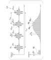
- FIG. FIG. 3 is a schematic diagram of an electric field distribution on the time axis (upper stage) and an intensity distribution on the frequency axis (lower stage) of an optical frequency comb
- 2 is a schematic diagram for explaining the principle of a wavefront synthesizing unit included in the wavefront control device shown in FIG. 1
- FIG. 3 is a schematic diagram for explaining how a wavefront synthesizing unit of the wavefront control device shown in FIG. 1 synthesizes wavefronts
- It is a schematic diagram of a wavefront measurement system of a 2nd embodiment concerning the present invention.
- FIG. 6 is a schematic diagram showing an example of a two-dimensional wavefront distribution of the wavefront measurement system shown in FIG. 5;
- FIG. It is a schematic diagram of a wavefront control device of a 2nd embodiment concerning the present invention.
- 8 is a schematic diagram showing an example of phase distribution of a plurality of optical pulses distributed on a predetermined plane of the wavefront control device shown in FIG. 7;
- FIG. FIG. 5 is a schematic diagram of a first modification of the wavefront control device according to the present invention;
- FIG. 5 is a schematic diagram of a second modification of the wavefront control device according to the present invention;
- FIG. 5 is a schematic diagram of a third modification of the wavefront control device according to the present invention;
- FIG. 11 is a schematic diagram for explaining how wavefront synthesis is performed in a wavefront synthesis section in a third modification of the wavefront control device according to the present invention;
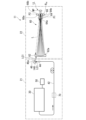
- a wavefront control device 11 includes an optical frequency comb generation section 21 and a wavefront synthesis section 22 .
- the optical frequency comb generation unit 21 generates an optical frequency comb (hereinafter sometimes referred to as an optical comb) LC1 and outputs the generated optical frequency comb LC1 toward the wavefront synthesis unit 22 .
- the optical frequency comb generator 21 includes at least an optical frequency comb generator 30 and a phase controller 50, and further includes an optical fiber 42, a fiber collimator 44, and a plane mirror 46.
- the optical frequency comb generator 30 generates one optical frequency comb LC1 and emits it from the emission end.
- the optical frequency comb LC1 has a plurality of optical pulses LP 1 , LP 2 , . . . , LP n , LP n+1 , . is an optical pulse train spaced apart by . n is an arbitrary natural number and represents the number of optical pulses on the time axis.
- LP n , LP n+1 , . . . are collectively referred to as a plurality of optical pulses LPn.
- the optical frequency comb LC1 has a plurality of optical pulses LPn arranged in numerical order on the time axis.
- a plurality of optical pulses LPn have longitudinal mode information on the frequency axis.
- Each light pulse LPn has a predetermined frequency distribution. The frequency of each light pulse LPn changes continuously on the time axis.
- a plurality of light pulses LPn oscillate at a constant repetition time Trep .
- the optical frequency comb LC1 on the time axis shown in the upper part of FIG. 2 is Fourier transformed and observed on the frequency axis, as shown in the lower part of FIG. modes are observed. That is, the optical frequency comb LC1 has a plurality of frequency modes FM 1 , FM 2 , . . . FM m , FM m+1 , . have m is an arbitrary natural number and represents a number on the frequency axis of the spectrum.
- the interval between the centers of the frequency modes FM m and FM m+1 adjacent to each other on the frequency axis is the repetition frequency f rep .
- the repetition time T rep is represented by equation (2).
- Each of the plurality of light pulses LPn is composed of a superposition of many longitudinal modes propagating inside the resonator of the light source.
- the optical frequency comb LC1 which is an optical pulse train, is composed of a carrier wave (also called a carrier), which is a superimposed wave of longitudinal modes, and a wave packet forming its envelope (also called an envelope). Since the velocity of the carrier wave and the velocity of the wave packet are different from each other, a phase difference occurs over time.
- a phase difference ⁇ n+1 represented by Equation (3) is present between the optical pulses LP n and LP n+1 adjacent to each other on the time axis. occur.
- the offset time T ceo of the optical frequency comb LC1 is represented by Equation (4).
- the phase shift that is, the period of the phase difference ⁇ n+1 , is one cycle at the offset time T ceo .
- the center frequency fn of the n-th frequency mode of the optical frequency comb LC1 is expressed by Equation (5) using the repetition frequency frep and the offset frequency fceo .
- the phase relationship of the plurality of optical pulses LPn can be freely set and controlled.
- the repetition frequency f rep and the offset frequency f ceo are stabilized with atomic clock level accuracy and are precisely locked to their respective predetermined values with high accuracy.
- the optical frequency comb generator 30 is configured to be capable of emitting an optical comb and independently controlling the repetition frequency f rep and the offset frequency f ceo of the emitted optical comb, as will be described later.
- the configuration of the optical frequency comb generator 30 may be changed as appropriate as long as the optical comb can be emitted and controlled as described above.
- the optical frequency comb generator 30 is, for example, a mode-locked laser diode (MLLD) resonator equipped with an erbium (Er) doped fiber, a polarization controller, and a delay controller. It is configured.
- MLLD mode-locked laser diode
- Er erbium
- the optical frequency comb generator 30 may be composed of, for example, an add/drop straight waveguide made of quartz on a glass substrate and a ring waveguide connected between the straight waveguides.
- the optical frequency comb generator 30 may be composed of a ring-shaped resonator made of silicon nitride on a silicon (Si) substrate.
- the optical frequency comb generator 30 may be composed of a toroidal microresonator in which a flange is provided at the tip of a protrusion on a Si substrate.
- the optical frequency comb generator 30 may be composed of a crystal resonator.
- the phase control unit 50 is connected to the optical frequency comb generator 30 and controls the repetition frequency f rep and the offset frequency f ceo of the optical frequency comb LC1 emitted from the optical frequency comb generator 30. do.
- the phase controller 50 is connected to, for example, a function generator (not shown) included in the optical frequency comb generator 30 .
- the function generator feeds a high frequency signal to the resonators that produce the optical frequency comb LC1 in the optical frequency comb generator 30 and directly affects the repetition frequency f rep and the offset frequency f ceo of the optical frequency comb LC1.
- the phase control unit 50 is provided for manipulating the output of the high-frequency signal of the function generator, and is, for example, a computer connected to the function generator. The details of the control of the repetition frequency f rep and the offset frequency f ceo by the phase control unit 50 will be described later.
- the incident side end of the optical fiber 42 is connected to the optical frequency comb generator 30 .
- the fiber collimator 44 is connected to the exit end of the optical fiber 42 .
- the fiber collimator 44 collimates the optical frequency comb LC ⁇ b>1 propagating through the optical fiber 42 and emits it toward the reflecting surface 46 a of the plane mirror 46 .
- the plane mirror 46 reflects the optical frequency comb LC ⁇ b>1 incident on the reflecting surface 46 a toward the wavefront synthesis unit 22 .
- the plane mirror 46 is provided with an adjustment mechanism 146 capable of rotating the reflecting surface 46a.
- the adjustment mechanism 146 is, for example, a rotary stage having a rotating shaft extending vertically through the central portion of the reflecting surface 46a in plan view and a motor for rotating the rotating shaft.
- the adjusting mechanism 146 rotates the reflecting surface 46a in the direction of the arrow, the angle of the optical frequency comb LC1 emitted from the reflecting surface 46a toward the wavefront synthesizing unit 22 changes.
- the wavefront synthesizing unit 22 synthesizes the plurality of optical pulses LPn contained in the incident optical frequency comb LC1 at a position P1 in the direction of travel of the optical frequency comb LC1 (that is, a position on the optical path of the optical frequency comb LC1 and a plane mirror 46 position of the output surface 46b), the light pulses LPn are distributed to different positions according to the phase ⁇ n of each light pulse LPn.
- a predetermined wavefront is formed by mutual interference of the phases ⁇ n of the optical pulses LPn distributed to different positions POn.
- the phase ⁇ n of the optical pulse LP n is controlled by the ratio between the repetition frequency f rep of the optical position frequency comb and the offset frequency f ceo .
- the relationship of the phases ⁇ n of the plurality of light pulses LPn on the time axis is converted into the relationship of the positions where each of the plurality of light pulses LPn is irradiated at the position P1.
- a plurality of optical pulses LPn distributed to positions different from each other at a predetermined position P1 are wavefront-combined on the exit side of the position P1 to form a combined wavefront WP.
- the wavefront synthesizing unit 22 is configured by an MPC optical system 60 that configures, for example, a multipass cavity (MPC).
- the MPC optical system 60 has a concave mirror 62 and a plane mirror 64 .
- the concave mirror 62 is arranged at a position where the optical frequency comb LC1 reflected by the plane mirror 46 of the optical frequency comb generator 21 can be directly incident.
- the concave mirror 62 is arranged ahead of the reflecting surface 46a of the plane mirror 46 in the traveling direction of the optical frequency comb LC1.
- the plane mirror 64 is arranged in front of the concave mirror 62 in the traveling direction of the optical frequency comb LC1 that enters the wavefront synthesizing section 22 and passes through the concave mirror 62 .
- the plano-convex lens 66 is arranged in front of the plane mirror 64 in the traveling direction of the optical frequency comb LC1 that enters the wavefront synthesis unit 22 and passes through the concave mirror 62 .
- the concave mirror 62 has a reflecting surface 62a that specularly reflects substantially all of the incident optical frequency comb LC1.
- the plane mirror 64 has a reflecting surface 64a that mirror-reflects part of the incident optical frequency comb LC1 and transmits at least part of the rest.
- the reflecting surface 64a faces the reflecting surface 62a in the traveling direction of the optical frequency comb LC1 (that is, on the optical axis).
- the concave mirror 62 and the plane mirror 64 constitute a resonator.
- Each of the concave mirror 62, the plane mirror 64, and the plano-convex lens 66 is made of a material that can transmit the optical frequency comb LC1, such as quartz or optical glass.
- Each of the reflecting surfaces 62a and 64a is formed of a dielectric multilayer film or a metal deposition film in consideration of the wavelength of the optical frequency comb LC1 and the like so as to exhibit the above-described transmission characteristics.
- the inter-reflecting-surface distance L between the reflecting surface 62a of the concave mirror 62 and the reflecting surface 64a of the plane mirror 64 is represented by equations (6) and (7).
- c represents the speed of light
- L rep represents the inter-pulse distance of the optical frequency comb LC1.
- the optical frequency comb LC1 that has entered the MPC optical system 60 first passes through the concave mirror 62 and travels toward the reflecting surface 64a of the plane mirror 64 in the outgoing direction D1.
- the optical pulse LPn +1 follows the optical pulse LPn in time series with a repetition time Trep . Therefore, the light pulse LP n is first incident on the reflecting surface 64a, and the light pulse LP n+1 is incident after the repetition time T rep has elapsed.
- Part of the optical frequency comb LC11 incident on the reflecting surface 64a is specularly reflected and travels in the backward direction D2 having a component opposite to the forward direction D1. At least a portion of the remaining optical frequency comb LC12 of the optical frequency comb LC1 incident on the reflecting surface 64a is transmitted through the plane mirror 64 .
- the optical frequency comb LC11 is specularly reflected by the reflecting surface 64a of the concave mirror 62, travels in the forward direction D1 again as the optical frequency comb LC2, and enters the reflecting surface 64a of the plane mirror 64.
- a part of the optical frequency comb LC21 of the optical frequency comb LC2 that has entered the reflecting surface 64a is mirror-reflected and travels in the backward direction D2 again.
- At least a part of the remaining optical frequency comb LC22 incident on the reflecting surface 64a is transmitted through the plane mirror 64 .
- the optical frequency comb LC21 is specularly reflected by the reflecting surface 62a of the concave mirror 62, travels in the forward direction D1 again as an optical frequency comb LC3 (not shown), and enters the reflecting surface 64a of the plane mirror 64.
- the optical frequency comb LCk is branched into the optical frequency comb LCk1 and the optical frequency comb LCk2 at the reflecting surface 64a of the plane mirror 64, similarly to the optical frequency combs LC1 and LC2.
- k represents a natural number of 3 or more. As k increases, the light amount of the optical frequency comb LCk decreases. In the MPC optical system 60, the branching from the optical frequency comb LCk to the optical frequency combs LCk1 and LCk2 is repeated as described above until the light amount of the optical frequency comb LCk is almost exhausted.
- an exit surface 64b of the plane mirror 64 opposite to the reflecting surface 64a is a surface that intersects the traveling direction (optical axis) of the optical frequency comb LC1 and the central axis AX of the resonator. It is arranged at a predetermined position P1 in the traveling direction of the comb LC1.
- a central axis AX passes through each center of the concave mirror 62 and the plane mirror 64 .
- the plurality of optical frequency combs LCp2 are incident on different positions of the exit surface 64b, pass through the exit surface 64b, and enter the plano-convex lens 66 (not shown in FIG. 4).
- p represents a natural number.
- Each of the plurality of optical frequency combs LCp2 corresponds to the phase ⁇ n along the circumferential direction around the central axis AX on the exit surface 64b and is emitted from positions different from each other.
- a plurality of light pulses LPn are distributed to different positions according to their phases ⁇ n .
- a plurality of light pulses LPn are distributed at different positions POn corresponding to phases ⁇ n along the circumferential direction about the central axis AX. .
- the radius of the annular distribution around the central axis AX when the multiple light pulses LPn are distributed is the shortest on the exit surface 64 b of the plane mirror 64 .
- the MPC optical system 60 Since the MPC optical system 60 is composed of a passive optical system, no time is required for mechanical driving.
- the optical frequency comb LC1 reciprocates between the concave mirror 62 and the plane mirror 64 and is split by the reflecting surface 64a of the plane mirror 64. They are distributed substantially simultaneously to different positions POn on the exit surface 64b.
- the timing at which the optical frequency comb LC1 reaches the exit surface 64b is such that the light pulse LPn passes through each of the different positions POn on the exit surface 64b of the plane mirror 64 only by the phenomenon at the speed of light described above. deviates.
- a plurality of light waves LW 1 , LW 2 , . . . having phases ⁇ 1 , ⁇ 2 , . , LW n , LW n+1 , . . . are emitted simultaneously.
- a plurality of light waves LWn interfere with each other and emit a light wave LL having a combined wavefront WP as shown in FIG.
- the positions POn from which the plurality of optical pulses LPn are emitted are determined by the phase difference ⁇ n+1 between the optical frequency combs LCp2.
- the incident position of the optical frequency comb LCp2 on the exit surface 64b changes depending on the angle formed by the traveling direction of the optical frequency comb LCp, which is multiple-reflected between the concave mirror 62 and the plane mirror 64, with respect to the central axis AX as described above.
- the curvature of the reflecting surface 62a of the concave mirror 62 is designed in consideration of the incident position of the optical frequency comb LCp2 on the output surface 64b.
- the incident position of the optical frequency comb LCp2 on the exit surface 64b is set and controlled by the relationship of the phase ⁇ n of the optical pulse LPn of the optical frequency comb LC1, as will be described later.
- Equation (3) the pulse-to-pulse phase difference ⁇ n+1 is expressed as in Equation (3).
- the pulse-to-pulse phase difference ⁇ n+1 is constant for all n and becomes a constant phase difference ⁇ if the repetition frequency f rep and the offset frequency f ceo are perfectly controlled.
- Equation (9) holds for the phases ⁇ n and ⁇ n+1 of the plurality of light waves LW n and LW n+1 .
- the phase difference ⁇ n+1 between the light waves LW n and LW n+1 is determined only by two parameters, the repetition frequency f rep and the offset frequency f ceo of the optical frequency comb LC1.
- the phase difference ⁇ n+1 is ( ⁇ n+1 ⁇ n ). If the repetition frequency f rep and the offset frequency f ceo are perfectly controlled, the phase difference ⁇ n+1 is constant regardless of n.
- the optical pulses LP n and LP adjacent on the time axis of the optical frequency comb LC1 The phase difference ⁇ between n+1 can be controlled.
- a light wave LL having a combined wavefront WP dependent on the phase difference ⁇ whose repetition frequency f rep and offset frequency f ceo are controlled by the phase control unit 50 is emitted from the exit surface 64b of the plane mirror 64 arranged at the position P1. .
- the synthesized wavefront WP depends on the phase difference ⁇ for which the repetition frequency f rep and the offset frequency f ceo are controlled by the phase controller 50 .
- the plurality of optical frequency combs LCp2 are transmitted through the plane mirror 64 and enter the plano-convex lens 66 arranged in front of the plane mirror 64 in the traveling direction of the plurality of optical frequency combs LCp2.
- the plano-convex lens 66 has a convex surface 66a and a flat surface 66b.
- the plano-convex lens 66 is arranged to assist in adjusting the optical axis of each of the plurality of optical frequency combs LCp2 emitted from the plane mirror 64, adjusting the spread direction of the beam, and causing the plurality of optical frequency combs LCp2 to interfere with each other.
- a compound lens such as a camera lens may be arranged in an auxiliary manner in place of the plano-convex lens 66 .
- the plano-convex lens 66 may be omitted when there is no need to adjust the optical axis or the spread direction of the beams in order to cause the plurality of optical frequency combs LCp2 to interfere with each other.
- the wavefront control device 11 of the first embodiment includes the optical frequency comb generation section 21 and the wavefront synthesis section 22 .
- the optical frequency comb generator 21 emits an optical frequency comb LC1 having a plurality of optical pulses LPn arranged in numerical order on the time axis.
- the optical frequency comb generation unit 21 includes a phase control unit 50 that controls the repetition frequency f rep and the offset frequency f ceo of the optical frequency comb LC1.
- the wavefront synthesizing unit 22 converts each of the plurality of light pulses LPn of the optical frequency comb LC1 incident from the optical frequency comb generating unit 21 onto the plane 66b of the plano-convex lens 66 (the plane intersecting with the traveling direction of the optical frequency comb) into the first Distribute to different positions PO n according to the phase ⁇ n relative to the optical pulse LP 1 (not shown in FIG. 2).
- the wavefront synthesizing unit 22 generates a synthesized wavefront WP of the light pulses LPn emitted from mutually different positions.
- the wavefront control device 11 of the first embodiment if the two parameters of the optical frequency comb LC1; the repetition frequency f rep and the offset frequency f ceo are each controlled to a predetermined value by the phase control unit 50 in the optical frequency comb generation unit 21, , a plurality of light pulses LPn arranged in numerical order on the time axis before entering the wavefront synthesizing section 22 can be distributed to the plane 66b of the plano-convex lens 66, ie, the transverse mode, at the speed of light.
- each optical pulse LPn when a plurality of optical pulses LPn are distributed, each optical pulse LPn is controlled only by the repetition frequency f rep and the offset frequency f ceo regardless of the number of distributions. It can be put into a state with information of the phase ⁇ n .
- the plane 66b of the plano-convex lens 66 can emit a combined wavefront WP formed by interference between the light pulses LPn each having a phase ⁇ n .
- waveguide-type optical phased arrays and conventional radio-wave phased arrays which are conventional wavefront control methods
- optical waves or radio waves are branched more than the number of optical waves or radio waves to be phase-controlled (i.e., the number of distributions), or a plurality of A wave source is provided to control the phase of each of a plurality of light waves and radio waves.
- the wavefront control device 11 of the first embodiment is completely different from waveguide-type optical phased arrays and conventional radio wave phased arrays, and has two control parameters for one optical frequency comb LC1 ; By controlling only the phase ⁇ n of the light pulse LP n delivered to the plane 66b of the plano-convex lens 66 is controlled.
- the wavefront control device 11 of the first embodiment unlike the conventional wavefront control method, there is no need to individually phase-control a plurality of distributed optical signals (that is, optical pulses LPn). It is not necessary to arrange a phase control unit for controlling the phase of each optical signal. In the wavefront control device 11 of the first embodiment, there is no need to calibrate the plurality of phase control units. From these, according to the wavefront control device 11 of the first embodiment, the wavefront can be controlled at high speed by a simple control operation of controlling the repetition frequency f rep and the offset frequency f ceo regardless of the increase in the number of antennas. It can be carried out. According to the wavefront control device 11 of the first embodiment, miniaturization can be achieved without depending on an increase in the number of antennas.
- one optical frequency comb LC1 is used as the optical signal of the optical antenna.
- the optical frequency comb LC1 has a broadband spectral distribution, as illustrated in the lower part of FIG.
- the frequencies f m of each of the plurality of frequency modes FM m forming the spectral distribution of the optical frequency comb LC1, that is, the repetition frequency f rep and the offset frequency f ceo are controlled with high accuracy. be able to.
- the wavefront controller 11 of the first embodiment before the phases ⁇ n of the plurality of optical pulses LPn forming the composite wavefront WP (that is, the phases ⁇ n of the optical antennas) are distributed at the position P1, the optical frequency The comb generator 21 can control the repetition frequency f rep and the offset frequency f ceo with high accuracy at the atomic clock level.
- the wavefront control device 11 of the first embodiment since the optical frequency comb LC1 has a wide spectrum distribution composed of a plurality of frequency modes FM m , it is possible to easily widen the band of the light wave to be controlled.
- the wavelength of the optical frequency comb LC1 emitted from the optical frequency comb generator 30 is converted in the optical frequency comb generator 21, thereby facilitating further broadening of the band of the light wave to be controlled.
- the wavelength converter 70 may be arranged in the middle of the optical fiber 42 of the optical frequency comb generator 21 .
- the wavelength converter 70 may be incorporated in the optical frequency comb generator 30, or may be provided between the fiber collimator 44 and the plane mirror 46 in a region through which the optical frequency comb LC1 passes.
- the wavelength conversion unit 70 converts the spectral distribution of the optical frequency comb LC1 into a visible wavelength range or an ultraviolet wavelength range other than the near-infrared wavelength range. Equipped with materials and crystals that can be converted into The configuration of the wavelength conversion section 70 may be changed as appropriate. However, the relationship between the phases ⁇ n of the optical pulses LPn in the optical frequency comb LC1 emitted from the wavelength converter 70 is maintained.
- the wavefront control device 11 of the first embodiment by further including the wavefront conversion unit 70, it is possible to realize wavefront control and adaptive optics of ultrashort light pulses from the deep ultraviolet wavelength region to the terahertz (THz) region, for example. .
- THz terahertz
- the wavefront synthesizing unit 22 includes an MPC optical system (resonator structure) 60 having a concave mirror 62 and a plane mirror 64 (a pair of mirrors) facing each other.
- the reflecting surface 62a of the concave mirror 62 specularly reflects substantially all of the incident optical frequency comb LCp.
- a reflecting surface 64a of the plane mirror (one mirror) 64 reflects part of the incident optical frequency comb LCp and transmits at least part of the rest.
- the inter-reflecting surface distance L between the reflecting surface 62a of the concave mirror 62 and the reflecting surface 64a of the plane mirror 64 is represented by the formula (1) (that is, the formula (6)), and is given by the repetition frequency f rep of the optical frequency comb LC1. controlled.
- the optical frequency comb LC1 that has entered the MPC optical system 60 which is a passive optical system, is reciprocated between the reflecting surfaces 62a and 64a, and is simultaneously and traveling from the reflecting surface 64a. It is possible to emit optical frequency combs LCp2 in which the numbers n of the optical pulses LPn are shifted from each other at the same position in the direction.
- the plurality of light pulses LPn possessed by the optical frequency comb LC1 are emitted at the exit surface 64b of the plane mirror 64 and the plane 66b of the planoconvex lens 66 according to the phase ⁇ n without mechanical driving. They can be distributed to different locations.
- the wavefront control device 11 of the first embodiment has an adjustment mechanism 146 .
- the adjusting mechanism 146 adjusts the incident angle of the optical frequency comb LC1 incident on the reflecting surface 64a of the plane mirror 64 (at least one mirror) of the concave mirror 62 and the plane mirror 64 (a pair of mirrors). By adjusting the angle of the reflecting surface 46a of the plane mirror 46 using the adjusting mechanism 146, the angle of the optical frequency comb LC1 incident on the plane mirror 64 can be changed to control the combined wavefront WP.
- the reflecting surface 62a of the concave mirror 62 is concave with respect to the flat reflecting surface 64a of the plane mirror 64 and the flat surface 66b of the plano-convex lens 66 .
- the optical frequency comb LC1 emitted from the optical frequency comb generator 21 enters the MPC optical system 60 so as to be substantially orthogonal to the reflecting surface 64a.
- the optical frequency comb LCp resonates between the concave mirror 62 and the plane mirror 64, and collects light from the reflecting surface 62a toward the reflecting surface 64a.
- a plurality of light pulses LPn can be distributed in the condensing region R 64 of the reflecting surface 64b at appropriate intervals and arrangement at which the combined wavefront WP is preferably formed. .
- a plurality of light pulses LPn are distributed to different positions on the exit surface 64b of the plane mirror 64 according to the phase ⁇ n . can do.
- the cavity length of the MPC optical system 60 depends on the repetition frequency f rep of the optical frequency comb LC1.
- the repetition frequency f rep of the optical frequency comb used is about 10 MHz to 1000 MHz.
- the distance L between the reflecting surfaces of the MPC optical system 60 is about several tens cm to 1 m. .
- the distance L between the reflecting surfaces of the MPC optical system 60 is about 10 GHz to 100 GHz. In this case, the distance L between the reflecting surfaces of the MPC optical system 60 can be suppressed to about several cm to 10 cm.
- the adaptive optics device 12 of the second embodiment includes the wavefront control device 11 of the first embodiment and an imaging optical system 13.
- the same reference numerals as those of the wavefront control device 11 of the first embodiment are given to the configurations that are common to the configuration of the wavefront control device 11 of the first embodiment.
- the description of the contents common to the description of the wavefront control device 11 of the first embodiment will be omitted.
- FIG. 5 shows a schematic configuration of only the exit surface 64b of the plane mirror 64 of the wavefront synthesizing section 22 in the wavefront control device 11.
- the imaging optical system 13 is arranged in front of the traveling direction D3 of the light wave LL formed from the exit surface 64b.
- the imaging optical system 13 includes a beam splitter 102 , condensing lenses 104 and 106 and an imaging camera 110 .
- the adaptive optics device 12 measures the wavefront using the imaging camera 110, and takes a clear image of the object S to be measured when wavefront compensation is achieved. Wavefront measurement may be performed by a device other than the adaptive optics device 12 illustrated in FIG.
- the measured object S to be measured is arranged in front of the traveling direction D3 of the light wave LL from the exit surface 64b.
- the beam splitter 102 and the condenser lens 104 are sequentially arranged between the plane mirror 64 and the object S to be measured in the traveling direction D3.
- the condenser lens 104 is arranged between the beam splitter 102 and the object S to be measured in the traveling direction D3.
- the beam splitter 102 transmits the light wave LL emitted from the emission surface 64b and incident along the traveling direction D3.
- the condenser lens 104 is arranged behind the measurement position PX on the surface of or inside the object S to be measured by the focal length in the traveling direction D3.
- the beam splitter 102 has a reflecting surface 102a.
- the reflecting surface 102a transmits the light wave LL incident from the traveling direction D3.
- the reflective surface 102a mirror-reflects the light wave LW incident from the opposite direction and substantially parallel to the traveling direction D3 toward the traveling direction D4 that intersects with the traveling direction D3.
- a condensing lens 106 and an imaging camera 110 are sequentially arranged ahead of the beam splitter 102 in the traveling direction D4.
- the light wave LL emitted from the exit surface 64b of the plane mirror 64 passes through the beam splitter 102 and travels along the traveling direction D3.
- the wavefront WP 1 of the light wave LL in the imaging optical system 13 propagates the same wavefront WP 0 as the combined wavefront WP generated by combining a plurality of light pulses LPn emitted from each of the optical antennas on the emission surface 64b. This is the wavefront that reaches the imaging optical system 13 through the
- the light wave LL transmitted through the beam splitter 102 is condensed at the measurement position PX by the condensing lens 104 .
- the light wave LW reflected from the measurement position PX includes information on the light wave LL and information on the object S to be measured.
- the wavefront WP2 of the light wave LW is a wavefront that is changed by the action of the optical characteristics of the object S to be measured on the wavefront WP1 .
- the wavefront WP1 is an ideal plane wave
- the wavefront WP2 is scattered by the object S to be measured and becomes a distorted wavefront, and the imaging camera 110 captures a distorted image. If a known wavefront is generated by the wavefront control device 11 and the wavefront WP2 is photographed as a reflected image, the optical characteristics of the object S to be measured can be specified.
- the wavefront controller 11 If the wavefront controller 11 generates the wavefront WP1 that compensates for the optical characteristics, the wavefront WP2 , which is the object light, is adjusted, and the image of the object S to be measured obtained by the imaging camera 110 becomes clear.
- the light wave LW reflected from the object S to be measured enters the condensing lens 104, is collimated, and travels substantially parallel to and opposite to the travel direction D3.
- the light wave LW enters the beam splitter 102 in a direction substantially parallel to and opposite to the traveling direction D3, and is specularly reflected in the traveling direction D4 by the reflecting surface 102a.
- the light wave LW reflected by the reflecting surface 102a travels along the travel direction D4, is condensed by the condensing lens 106, and is received by the imaging camera 110.
- the wavefront WP2 of the light wave LW reflecting the optical characteristics of the object S to be measured travels in the direction substantially parallel to and opposite to the direction of travel D3
- the repetition frequency f rep and the offset frequency f ceo of the optical frequency comb LC1 are controlled by the phase control unit 50 of the wavefront controller 11 so as to obtain an orthogonal and substantially flat wavefront.
- the adaptive optics device 12 of the second embodiment described above includes the wavefront control device 11 of the first embodiment and the imaging optical system 13 .
- the imaging optical system 13 is configured to irradiate the object S to be measured with the light wave LL emitted from the wavefront control device 11 and to receive the light wave LW reflected or transmitted from the object S to be measured.
- the phase control unit 50 of the wavefront control device 11 controls only two control parameters of the optical frequency comb LC1 ;
- the wavefront WP1 of the light wave LL that irradiates the measurement object S can be freely controlled.
- the wavefront WP2 can be freely controlled.
- the repetition frequency f rep and the offset frequency f ceo of the optical frequency comb LC1 controlled using the information obtained from the light wave LW received by the imaging optical system 13 and the phase control unit 50 are
- the optical characteristics of the object S to be measured at the measurement position PX can be measured based on the relationship of .
- the wavefront WP2 of the light wave LW reflected or transmitted (reflected in FIG. 5) from the object S to be measured becomes a flat wavefront orthogonal to the optical axis.
- Only two control parameters of the optical frequency comb LC1 can be controlled by the phase controller 50 of the wavefront controller 11: the repetition frequency f rep and the offset frequency f ceo .
- the causal relationship between the wavefront WP1 of the light wave LL and the wavefront WP2 of the light wave LW and the optical characteristics of the object S to be measured at the measurement position PX is caused by the influence of air fluctuation, heat, etc. in the imaging optical system 13, for example. turbulence may occur.
- the wavefront WP2 is flattened, and the imaging camera 110 can acquire a high-contrast image and highly accurate measurement data.
- a plurality of phases ⁇ n of light are emitted from a plurality of positions POn acting as optical antennas to form wavefronts WP 0 .
- the adaptive optical device 12 of the second embodiment it is not necessary to individually control each of the phases ⁇ n of a plurality of lights as in the prior art.
- the wavefront WP2 of the light wave LW can be compensated.
- the wavelength conversion unit 70 is provided in the optical frequency comb generation unit 21 of the wavefront control device 11, so that the optical frequency comb LC1 in the stage preceding the installation position of the wavelength conversion unit 70 is Wavelength conversion is possible.
- adaptive optics can be realized with ultrashort pulses from the deep ultraviolet wavelength range to the THz range, for example.
- Adaptive optics using the adaptive optics device 12 of the second embodiment enables, for example, realization of direct fluorescence measurement with higher efficiency than conventional ones, or application to multiphoton absorption measurement and multiphoton microscopy.
- the adaptive optical device 12 of the second embodiment can be used for the purpose of evaluating the transverse mode characteristics of light waves in addition to the purpose of realizing adaptive optics as described above.
- a light emitting unit of a complicated optical system constituting an optical communication system, an optical functional device, or the like may be arranged to measure emitted light.
- the emitted light and the wavefront generated by the wavefront control device 11 may interfere with each other.
- the light wave LL emitted from the exit surface 64b of the plane mirror 64 at the position P1 is a two-dimensional plane that intersects the optical axis, and the repetition frequency f rep and the offset frequency f are controlled by the phase control unit 50.
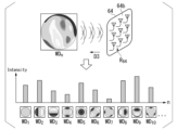
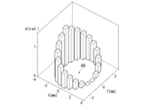
- the bottom of FIG. 6 shows several pattern examples of two-dimensional wavefront distributions WD 1 , WD 2 , .
- the wavefront of the light wave LW reflected or transmitted from the light emitting part of the complicated optical system is received as it is without compensation, and the light intensity of the light wave LW is measured. You can see what kind of action the optical system received. From this, it is possible to know what kind of combination of simple wavefronts the light wave LW was generated, and to accurately evaluate the transverse mode characteristics of a complicated optical system or the like.
- two-dimensional wavefront distributions WD 1 , WD 2 . You can determine if it is included.
- the adaptive optics device 12 of the second embodiment suitably functions as a wavefront analyzer or two-dimensional spectroscope for evaluating transverse modes.
- a feedback mechanism 150 is provided in the wavefront control device 11 of the first embodiment.
- the feedback mechanism 150 includes a beam splitter 152 and a photodiode (PD) 154 .
- the beam splitter 152 is arranged in a region through which the optical frequency comb LCp2 passes between the plane mirror 64 and the plano-convex lens 66 of the wavefront synthesizing unit 22, and is arranged on the central axis AX between the plane mirror 64 and the plano-convex lens 66. there is
- the beam splitter 152 has a reflecting surface 152a.
- a portion of the optical frequency comb LCp2 incident on the beam splitter 152 is mirror-reflected by the reflecting surface 152a in a traveling direction D3 substantially perpendicular to the forward direction D1 and the backward direction D2.
- At least part of the remaining portion of the optical frequency comb LCp2 that has entered the beam splitter 152 passes through the reflecting surface 152a and enters the plano-convex lens 66 .
- a plurality of light pulses LPn are distributed to positions POn different from each other according to the phase ⁇ n .
- a light wave LL having a combined wavefront WP is emitted from an emission surface 64 b of the plane mirror 64 .
- the photodiode 154 receives the optical frequency comb LCp2 reflected by the reflecting surface 152a of the beam splitter 152 in the traveling direction D3.
- the photodiode 154 and the phase controller 50 of the optical frequency comb generator 21 are electrically connected by wire or wirelessly.
- the photodiode 154 outputs an electrical signal corresponding to the amount of light received from the optical frequency comb LCp2 to the phase controller 50 in real time.
- FIG. 7 shows only the repetition frequency control unit 161, the offset frequency control unit 162, the frequency dividers 165 and 166, and the mixer 170 of the device configuration of the optical frequency comb generation unit 21 of the wavefront control device 15.
- the repetition frequency control unit 161 receives the electrical signals obtained by the feedback mechanism 150 and the phase control unit 50, synchronizes with the distance L between the reflecting surfaces of the MPC optical system 60, and adjusts the repetition frequency f rep of the optical frequency comb LC1. Control.
- the offset frequency control unit 162 generates and controls the offset frequency f ceo of the optical frequency comb LC1.
- the repetition frequency f rep controlled by the repetition frequency control section 161 is input to the frequency divider 165 and divided into (1/ ⁇ ).
- the output from the offset frequency control section 162 is input to the frequency divider 166 and divided into (1/ ⁇ ). Outputs from frequency dividers 165 and 166 are input to mixer 170 and recursively input from mixer 170 to offset frequency control section 162 .
- the offset frequency control section 162 controls the offset frequency f ceo according to the recursively input signal.
- the offset frequency control section 162 controls the repetition frequency f rep so as to stabilize the MPC optical system 60 . If the phase control unit 50 operates to control the offset frequency f ceo with respect to the repetition frequency f rep , the frequency ratio between the repetition frequency f rep and the offset frequency f ceo can be controlled according to equation (10).
- FIG. 8 shows the result of numerical calculation of the phase distribution of the plurality of light pulses LPn distributed on the exit surface 64b of the plane mirror 64 of the wavefront synthesizing unit 22.
- the X-axis and the Y-axis in FIG. 8 represent two directions that are included in the output surface 64b when the origin is the position where the output surface 64b intersects the central axis AX, and are orthogonal to each other.
- the vertical axis in FIG. 8 represents the phase ⁇ n . As shown in FIG.
- a phase distribution is formed on the output surface 64b along the circumferential direction around the central axis AX.
- a plurality of phases ⁇ n of the phase distribution formed around the central axis AX continuously increase and decrease in the circumferential direction to form a virtual inclined plane.
- a light wave LL generated from the light pulse LPn is emitted in a direction substantially orthogonal to the inclined surface.
- the phase control unit 50 can freely and quickly control the phase distribution of the plurality of light pulses LPn on the exit surface 64b.
- the phase control unit 50 controls at least the repetition frequency f rep of the optical frequency comb LC1, and controls the ratio parameter ; , the inclined surface of the phase distribution of the plurality of light pulses LPn and the emission direction of the light waves LL on the emission surface 64b can be set freely and with high accuracy.
- a plurality of light pulses LPn are distributed by the MPC optical system 60 having the concave mirror 62 and the plane mirror 64.
- a phase distribution is formed in the circumferential direction around the central axis AX at 64b.
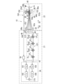
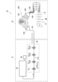
- a wavefront control device 15 of the third embodiment includes a feedback mechanism 150 .
- the feedback mechanism 150 is composed of a plurality of beams emitted from the plane mirror 64 and distributed to different positions according to the phase ⁇ n on the exit surface 64b. is fed back to the phase controller 50 of the optical frequency comb generator 21 .
- the phase control unit 50 compares the received intensity information of the optical pulses LPn of the plurality of optical frequency combs LCp2 with the known intensity information of the optical pulses LPn of the optical frequency comb LC1.
- the phase control unit 50 By using the phase control unit 50, it is possible to check in real time whether or not the phase distribution of the optical pulses LPn of the optical frequency comb LCp2 is fluctuating or disturbed due to environmental changes such as air fluctuations. Two parameters of the optical frequency comb LC1 in the optical frequency comb generation unit 21 using the phase control unit 50 when it is determined that there is fluctuation or disturbance in the phase distribution of the optical pulses LPn of the optical frequency comb LCp2; By controlling only the frequency f rep and the offset frequency f ceo , fluctuations and disturbances in the phase distribution can be eliminated. According to the wavefront control device 15 of the third embodiment, the repetition frequency f rep of the optical frequency comb LC1 can be synchronized with the cavity length of the MPC optical system 60 to stabilize the optical antenna.
- the wavefront control device 15 of the third embodiment can be applied to ultra-precise three-dimensional surveying by focal point scanning on a plane that intersects the traveling direction of the light wave LL and the central axis AX.
- the wavefront control device 15 of the third embodiment can be applied to ultra-precise three-dimensional surveying by absolute distance measurement in the traveling direction of the light wave LL and the depth direction substantially parallel to the central axis AX.
- the wavefront control device 15 of the third embodiment can be used to three-dimensionally scan the object S to be measured having a spherical surface, and the shortest distance to the spherical surface can be calculated by surface measurement.
- the Avogadro constant can be determined, for example, by profilometry of silicon spheres.
- three-dimensional LiDAR can be realized by performing measurement in the depth direction at the same time as scanning the focal point using the wavefront control device 15 of the third embodiment.
- the beam splitter 152 of the feedback mechanism 150 is arranged between the plane mirror 64 and the plano-convex lens 66 of the MPC optical system 60 .
- the beam splitter 152 may be arranged in a region through which the optical frequency comb LCp reflected by the reflecting surface 64a of the plane mirror 64 passes, as indicated by a two-dot chain line in FIG.
- the MPC optical system 60 having the concave mirror 62 and the plane mirror 64 is used. It changes circumferentially with respect to the time change in the circumferential direction. In order to stop the circular change, an inverted distribution obtained by inverting the phase distribution of the plurality of optical pulses LPn should be imparted to the phase distribution of the plurality of optical pulses LPn.
- the adaptive optics device 12 of the second embodiment may include the wavefront control device 15 of the third embodiment instead of the wavefront control device 11 of the first embodiment.
- the wavefront synthesizing unit of the wavefront control device according to the present invention may have a passive optical antenna structure other than the MPC optical system.
- a wavefront control device 17 shown in FIG. 9 and a wavefront control device 18 shown in FIG. 10 are given as first and second modifications of the wavefront control device according to the present invention.
- the optical frequency comb generator 21 of the wavefront controller 17 includes an optical frequency comb generator 30 , a phase controller 50 , an optical fiber 42 and an optical fiber coupler 180 .
- the wavefront synthesizing unit 22 of the wavefront control device 17 includes a plurality of output waveguides 182 instead of the MPC optical system 60 of the wavefront control devices 11 and 15 .
- the input side end of the optical fiber coupler 180 is connected to the output side end of the optical fiber 42 .
- the output side end of the optical fiber coupler 180 is connected to the input side ends of the plurality of output waveguides 182 .
- the plurality of output waveguides 182 are composed of output waveguides having different optical path lengths.
- the optical path length difference between the output waveguides 182 is equal to the optical path length difference when the optical pulses LP n and LP n+1 adjacent to each other on the time axis of the optical frequency comb LC1 propagate through the output waveguide 182 .
- the optical frequency combs LC1 whose numbers of the optical pulses LPn are different from each other are emitted at the same time.
- the wavefront control device 17 of the first modification similarly to the wavefront control devices 11 and 15, the plurality of optical pulses LPn of the optical frequency comb LC1 are shifted to different positions according to the phase ⁇ n without mechanical driving. It can be distributed to the output-side ends of a plurality of provided output waveguides 182 . According to the wavefront control device 17 of the first modified example, effects similar to those of the wavefront control devices 11 and 15 can be obtained.
- the optical frequency comb generator 21 of the wavefront controller 18 includes an optical frequency comb generator 30, a phase controller 50, and an optical fiber .
- the wavefront synthesizing unit 22 of the wavefront controller 18 includes an arrayed-waveguide grating (AWG) 190 instead of the MPC optical system 60 of the wavefront controllers 11 and 15 .
- the arrayed waveguide diffraction grating 190 includes an input waveguide 191 connected to the output-side end of the optical fiber 42, an input-side slab waveguide 192, an arrayed waveguide group 193, an output-side slab waveguide 194, and a plurality of output waveguides 195 .
- the optical frequency comb LC1 emitted from the optical fiber 42 is diffracted by the input-side slab waveguide 192 via the input waveguide 191, enters the arrayed waveguide group 193, and is independent for each waveguide of the arrayed waveguide group 193. propagating along the optical path.
- the optical path length difference between the waveguides of the arrayed waveguide group 193 corresponds to the optical path length difference when the optical pulses LP n and LP n+1 adjacent to each other on the time axis of the optical frequency comb LC1 propagate through the output waveguide 182. depends.
- the optical frequency comb LC1 emitted from the arrayed waveguide group 193 undergoes multiple interference in the output side slab waveguide 194, and converges on the incident side ends of the output waveguides 195 which are different for each wavelength.
- optical frequency combs LC1 whose numbers n of the optical pulses LPn are different from each other are emitted at the same time.
- a plurality of optical pulses LPn possessed by the optical frequency comb LC1 are shifted to different positions according to the phase ⁇ n without mechanical driving. It can be distributed to output ends of a plurality of provided output waveguides 195 . According to the wavefront control device 18 of the second modified example, effects similar to those of the wavefront control devices 11 and 15 can be obtained.
- a wavefront control device 81 shown in FIG. 11 there is a wavefront control device 81 shown in FIG. 11 in a wavefront control device 81, an intensity modulator (IM) 160 is provided in the wavefront control device 15 of the third embodiment.
- the intensity modulator 160 is arranged on the path of the optical frequency comb LC1 between the optical frequency comb generator 30 and the fiber collimator 44, and arranged in the middle of the optical fiber 42 of the optical frequency comb generator 21.
- the intensity modulator 160 thins out a predetermined optical pulse out of the plurality of optical pulses LPn of the optical frequency comb LC1 that are emitted from the optical frequency comb generator 30 and are incident via the optical fiber 42 .
- FIG. 11 an intensity modulator 160 is provided in the wavefront control device 15 of the third embodiment.
- the intensity modulator 160 is arranged on the path of the optical frequency comb LC1 between the optical frequency comb generator 30 and the fiber collimator 44, and arranged in the middle of the optical fiber 42 of the optical
- the intensity modulator 160 thins out the light pulses LC n+3 , LC n+6 , and LC n+7 out of the light pulses LC n+1 to LC n+8 which are part of the optical frequency comb LC1.
- predetermined light pulses out of the plurality of light pulses LPn of the optical frequency comb LC1 are thinned out by the intensity modulator 160, as shown in FIG. placement changes.
- the phase distribution formed on the exit surface 64b of the plane mirror 64 is a predetermined value based on the principle described with reference to FIG.
- the light wave LL generated from the optical frequency comb LC1 is emitted in a direction substantially perpendicular to the inclined plane of the phase distribution formed on the emission surface 64b.
- the plurality of light pulses LPn remaining after predetermined light pulses of the optical frequency comb LC1 are thinned out from the plane 66b of the plano-convex lens 66 in the wavefront synthesizing unit 22 interfere with each other.
- a composite wavefront WP consisting of For example, when the light pulses LC n+3 , LC n+6 and LC n +7 are thinned out by the intensity modulator 160 as shown in FIG.
- a composite wavefront WP generated by the interference of n+5 and LC n+8 is emitted.
- the wavefront WP 0 of the light wave LL ie, the two-dimensional wavefront distribution of the synthesized wavefront WP, is based on the light pulses remaining after predetermined light pulses are thinned out.
- a predetermined optical pulse to be thinned out by the intensity modulator 160 is calculated from the combined wavefront WP output from the wavefront combining section 22 and appropriately set. For this reason, in order to obtain a composite wavefront WP and a two-dimensional wavefront distribution of a specific transverse mode, the intensity modulator 160 modulates a specific transverse mode among the plurality of optical pulses LPn of the incident optical frequency comb LC1. thin out predetermined light pulses.
- the wavefront control device 81 of the third modification sends some of the optical pulses LCn of the optical frequency comb LC1 emitted from the optical frequency comb generator 21 to the wavefront synthesis unit 22. It has an intensity modulator 160 that emits towards. A portion of the optical pulse emitted from the intensity modulator 160 is obtained by back calculation from the desired transverse mode of the combined wavefront WP generated by the wavefront combining section 22 . According to the wavefront control device 81 of the third modified example, it is possible to generate and utilize a high-order transverse mode from a phase distribution having a high degree of freedom of control.
- the wavefront control device 81 of the third modified example can calculate the phase distribution that expresses the high-order transverse mode and control the phase distribution using the intensity modulator 160 .
- the wavefront control device 81 of the third modified example it is possible to appropriately find the correspondence between a plurality of phases ⁇ n emitted from a plurality of positions POn functioning as optical antennas. Further, by interfering not only with the synthesized wavefront WP formed by the thinned-out pulse train, but also with another synthesized wavefront WP that is subsequently formed, a more complicated high-order transverse mode can be formed.
- a resonator having the same resonator length as that of the MPC optical system 60 is arranged ahead of the plano-convex lens 66 in the traveling direction of the combined wavefront WP, and pulse stacking is performed using the resonator.
- the resonator placed in front of the MPC optical system 60 may be a spatial optical system such as the MPC optical system 60, or may be configured by an arrayed waveguide group, a bundle fiber in which a large number of fibers are bundled, or the like. .
Abstract
A wavefront control device to which the present invention is applied is provided with: an optical frequency comb generation unit that emits an optical frequency comb having a plurality of optical pulses disposed in numerical order on a time axis; and a wavefront synthesis unit that distributes the plurality of optical pulses of the optical frequency comb incident from the optical frequency comb generation unit to positions different from each other according to the relative phases thereof with respect to the first optical pulse on a plane crossing the traveling direction of the optical frequency comb, and generates a synthesized wavefront of the optical pulses emitted from the positions different from each other. The optical frequency comb generation unit is provided with a phase control unit that controls the repetition frequency and offset frequency of the optical frequency comb.
Description
本発明は、波面制御装置及び補償光学装置に関する。本願は、2021年8月25日に、日本に出願された特願2021-137394号に基づき優先権を主張し、その内容をここに援用する。
The present invention relates to wavefront control devices and adaptive optics devices. This application claims priority based on Japanese Patent Application No. 2021-137394 filed in Japan on August 25, 2021, the content of which is incorporated herein.
従来、被計測物体の形状測定や断層像の取得、構造解析等が行われる際に、補償光学によって撮影像が補正及び回復される。被計測物体から取得された直接像は、環境や空間のゆらぎの影響を受けて歪んだ像になる。この歪んだ像が波面制御によって補正されることによって撮像カメラ等の受光器の撮像面に高いコントラストで結像する鮮明な像が得られる。補償光学を用いた測定では、取得された波面の形状や状態を計測する波面計測と、計測された波面に関する情報に基づいて波面を制御する波面制御が行われる。
Conventionally, when measuring the shape of an object to be measured, obtaining a tomographic image, structural analysis, etc., the captured image is corrected and restored by adaptive optics. A direct image obtained from an object to be measured becomes a distorted image under the influence of environmental and spatial fluctuations. By correcting this distorted image by wavefront control, a clear image formed with high contrast on the imaging surface of a light receiver such as an imaging camera can be obtained. In the measurement using adaptive optics, wavefront measurement for measuring the shape and state of the acquired wavefront and wavefront control for controlling the wavefront based on information on the measured wavefront are performed.
波面計測を行う技術として、例えばレンズアレイを備えたシャックハルトマン波面センサ(Shack-Hartmann wavefront sensor)を用いる方法、入射する光の光軸に対して交差する反射面の向きを調整可能な可変ミラーを用いる方法、或いは空間位相変調器(spatial light modulator;SLM)によって入射する波面の位相を直接変調する方法が知られている。前述の各方法に基づく測定技術は確立されているが、波面計測の応答速度は数10Hzオーダーであり、波面制御の応答速度は数10kHzオーダーである。そのため、従来よりも高速に波面計測及び波面制御を行う方法が検討されていた。
Wavefront measurement techniques include, for example, a method using a Shack-Hartmann wavefront sensor equipped with a lens array, and a variable mirror capable of adjusting the orientation of the reflecting surface that intersects the optical axis of incident light. or directly modulating the phase of the incident wavefront by means of a spatial light modulator (SLM). Measurement techniques based on the above methods have been established, but the response speed for wavefront measurement is on the order of several tens of Hz, and the response speed for wavefront control is on the order of several tens of kHz. Therefore, a method of performing wavefront measurement and wavefront control at a higher speed than before has been studied.
波面計測及び波面制御の高速化を図るためのアプローチとして、フェーズドアレイが挙げられる。フェーズドアレイアンテナは、アレイ状に配置された複数のアンテナと位相制御された電磁波によって実現され、電磁波として電波を用いた気象レーダーや超音波診断機に用いられている。フェーズドアレイアンテナを用いることによって、複数のアンテナから個別に制御された位相を有する電磁波が射出されるので、波面計測と波面制御とを同時に行うことができる。近年、電磁波として光を用いる光フェーズドアレイは、LiDAR(light detection and ranging)、プロジェクター及び生体蛍光計測への応用が期待されている。
A phased array is an approach to speed up wavefront measurement and wavefront control. A phased array antenna is realized by a plurality of antennas arranged in an array and phase-controlled electromagnetic waves, and is used in weather radars and ultrasonic diagnostic equipment that use radio waves as electromagnetic waves. By using a phased array antenna, electromagnetic waves having individually controlled phases are emitted from a plurality of antennas, so wavefront measurement and wavefront control can be performed at the same time. In recent years, optical phased arrays that use light as electromagnetic waves are expected to be applied to LiDAR (light detection and ranging), projectors, and biological fluorescence measurement.
例えば、特許文献1及び非特許文献1,2には、光フェーズドアレイの一例として導波路型の光集積回路デバイスが開示されている。これらの光集積回路デバイスでは、平面光波回路等に形成された入力導波路からアンテナと同数に分岐された複数の分岐導波路の各々に位相調整部が設けられている。位相調整部で位相制御された光波は、複数の分岐導波路の各々の出射端部(アンテナ)から出射される。
For example, Patent Document 1 and Non-Patent Documents 1 and 2 disclose a waveguide type optical integrated circuit device as an example of an optical phased array. In these optical integrated circuit devices, each of a plurality of branch waveguides branched from an input waveguide formed in a planar lightwave circuit or the like in the same number as the antennas is provided with a phase adjustment section. The lightwave phase-controlled by the phase adjuster is emitted from the emission end (antenna) of each of the plurality of branch waveguides.
従来の光フェーズドアレイは、上述の特許文献1及び非特許文献1,2で例示したように導波路型の光集積回路デバイスで構成されている。しかしながら、導波路型の光集積回路デバイスでは、分岐導波路と同数の位相調整部、すなわち光フェーズドアレイのアンテナ数と同数の位相調整部の各々を個別に制御する必要がある。アンテナ数の増大に伴い、複数の位相調整部及びこれらの各々に接続される位相制御装置等が占めるスペースが増大する。アンテナ数の2倍程度のパラメータを互いに独立に制御及び校正する必要があり、アンテナ数の増大に伴い、複数のアンテナの制御及び各アンテナのパラメータの校正が煩雑になる。導波路型の光集積回路デバイスにおける導波路での光波の伝搬特性の低下を抑えるためには、実質的に単色光を使わざるを得ない。前述のように、従来の導波路型の光フェーズドアレイによって波面計測及び波面制御を行う対象の光波を広帯域化し、高速に制御するためには、集積回路及び制御装置の大型化と、制御パラメータの増大が不可避である。このことから、従来の導波路型の光フェーズドアレイの実用性は低かった。
Conventional optical phased arrays are composed of waveguide-type optical integrated circuit devices, as exemplified in Patent Document 1 and Non-Patent Documents 1 and 2 above. However, in waveguide-type optical integrated circuit devices, it is necessary to individually control the same number of phase adjustment units as there are branch waveguides, that is, the same number of phase adjustment units as the number of antennas in the optical phased array. As the number of antennas increases, the space occupied by a plurality of phase adjustment units and phase control devices connected to each of them increases. It is necessary to independently control and calibrate parameters about twice as many as the number of antennas. As the number of antennas increases, control of a plurality of antennas and calibration of parameters for each antenna become complicated. In order to suppress the deterioration of the propagation characteristics of light waves in waveguides in waveguide type optical integrated circuit devices, substantially monochromatic light has to be used. As described above, in order to broaden the band of the light wave to be subjected to wavefront measurement and wavefront control by the conventional waveguide type optical phased array and to control it at high speed, it is necessary to increase the size of the integrated circuit and the control device, and to increase the control parameters. Growth is inevitable. For this reason, the practicality of the conventional waveguide-type optical phased array was low.
本発明は、アンテナ数の増加に依らず簡便な制御によって高速に波面制御を行い、且つ制御対象の光波の広帯域化を実現可能な波面制御装置及び補償光学装置を提供する。
The present invention provides a wavefront control device and an adaptive optics device capable of performing high-speed wavefront control with simple control regardless of an increase in the number of antennas, and realizing widening the bandwidth of light waves to be controlled.
本実施形態に係る波面制御装置は、時間軸上で番号順に配置された複数の光パルスを有する光周波数コムを出射する光周波数コム生成部と、前記光周波数コム生成部から入射する前記光周波数コムの前記複数の光パルスの各々を前記光周波数コムの進行方向に交差する面で1番目の前記光パルスに対する相対的な位相に応じて互いに異なる位置に分配し、前記互いに異なる位置から出射する前記光パルス同士の合成波面を生成する波面合成部と、を備える。前記光周波数コム生成部は、前記光周波数コムの繰り返し周波数とオフセット周波数とを制御する位相制御部を備える。
The wavefront control device according to the present embodiment includes an optical frequency comb generator that emits an optical frequency comb having a plurality of optical pulses arranged in numerical order on a time axis, and the optical frequency comb that is incident from the optical frequency comb generator. Each of the plurality of optical pulses of the comb is distributed to positions different from each other according to a phase relative to the first optical pulse on a plane intersecting the traveling direction of the optical frequency comb, and emitted from the positions different from each other. and a wavefront synthesizing unit that generates a synthetic wavefront of the optical pulses. The optical frequency comb generator includes a phase controller that controls the repetition frequency and offset frequency of the optical frequency comb.
本実施形態に係る波面制御装置では、前記波面合成部は、互いに対向配置された一対のミラーを有する共振器構造を備えてもよい。前記一対のミラーのうち一方のミラーの反射面は、入射する前記光周波数コムの一部を反射し、且つ残部の少なくとも一部を透過してもよい。前記一対のミラーを1往復した前記光パルス同士の合成波面を考慮した場合には、前記一対のミラーの反射面間距離Lは、(1)式で表される。
In the wavefront control device according to this embodiment, the wavefront synthesizing section may include a resonator structure having a pair of mirrors arranged to face each other. A reflective surface of one of the pair of mirrors may reflect a portion of the incident optical frequency comb and transmit at least a portion of the remainder. Considering the combined wavefront of the light pulses that have made one reciprocation on the pair of mirrors, the distance L between the reflecting surfaces of the pair of mirrors is expressed by Equation (1).
上述の(1)式におけるLrepは前記光周波数コムのパルス間距離を表し、cは光速を表し、frepは前記光周波数コムの繰り返し周波数を表す。
L rep in the above equation (1) represents the pulse-to-pulse distance of the optical frequency comb, c represents the speed of light, and f rep represents the repetition frequency of the optical frequency comb.
本実施形態に係る波面制御装置は、前記一対のミラーのうち少なくとも一方のミラーに入射する前記光周波数コムの入射角度を調節する調節機構を備えてもよい。前記一対のミラーが用いられた場合には、少なくとも一方のミラーに入射する角度が変化し、合成波面が制御されてもよい。
The wavefront control device according to this embodiment may include an adjustment mechanism for adjusting the incident angle of the optical frequency comb incident on at least one of the pair of mirrors. When the pair of mirrors is used, the angle of incidence on at least one of the mirrors may be changed to control the synthesized wavefront.
本実施形態に係る波面制御装置では、前記光周波数コム生成部は、前記光周波数コムの波長を変換する波長変換部を備えてもよい。前記光パルス同士の合成波面は1往復したパルスではなく、任意の回数往復したパルス間の干渉を用いて合成波面が構成されてもよい。
In the wavefront control device according to this embodiment, the optical frequency comb generator may include a wavelength converter that converts the wavelength of the optical frequency comb. The composite wavefront of the optical pulses may be formed by using interference between pulses that have made an arbitrary number of round trips instead of the pulse that has made one round trip.
本実施形態に係る波面制御装置は、前記合成波面を有する光波の強度情報を前記位相制御部にフィードバックするフィードバック機構を備えてもよい。
The wavefront control device according to the present embodiment may include a feedback mechanism that feeds back intensity information of the light wave having the composite wavefront to the phase control section.
本実施形態に係る波面制御装置において、前記位相制御部は、前記繰り返し周波数と前記オフセット周波数との比率を所定値に設定してもよい。
また、本実施形態に係る波面制御装置は、前記光周波数コム生成部から出射された前記複数の光パルスのうちの一部の光パルスを前記波面合成部に向けて出射する強度変調器を備えてもよい。 In the wavefront control device according to this embodiment, the phase control section may set a ratio between the repetition frequency and the offset frequency to a predetermined value.
Further, the wavefront control device according to the present embodiment includes an intensity modulator that emits a portion of the plurality of optical pulses emitted from the optical frequency comb generator toward the wavefront synthesizing unit. may
本実施形態に係る補償光学装置は、前記波面制御装置と、イメージング光学系と、を備える。前記イメージング光学系は、前記波面制御装置の前記波面合成部から出射されて前記合成波面を有する光波を被計測物体に照射可能に構成され、前記被計測物体から反射又は透過した光波を受光可能に構成されている。
An adaptive optics device according to this embodiment includes the wavefront control device and an imaging optical system. The imaging optical system is configured to be capable of irradiating an object to be measured with a light wave having the synthesized wavefront emitted from the wavefront synthesizing unit of the wavefront control device, and capable of receiving a light wave reflected or transmitted from the object to be measured. It is configured.
本発明に係る波面制御装置及び補償光学装置によれば、アンテナ数の増加に依らず簡便な制御によって高速に波面制御を行い、且つ制御対象の光波の広帯域化を実現することができる。
According to the wavefront control device and the adaptive optics device according to the present invention, it is possible to perform wavefront control at high speed through simple control without depending on an increase in the number of antennas, and to achieve a wide band of light waves to be controlled.
以下、本発明に係る波面制御装置及び補償光学装置の実施形態について、図面を参照して説明する。
Embodiments of a wavefront control device and an adaptive optical device according to the present invention will be described below with reference to the drawings.
[第1実施形態]
図1に示すように、本発明に係る第1実施形態の波面制御装置11は、光周波数コム生成部21と、波面合成部22と、を備える。光周波数コム生成部21は、光周波数コム(以下、光コムという場合がある)LC1を生成し、生成した光周波数コムLC1を波面合成部22に向けて出射する。光周波数コム生成部21は、少なくとも光周波数コム発生器30と、位相制御部50と、を備え、光ファイバ42と、ファイバコリメータ44と、平面鏡46と、をさらに備える。 [First embodiment]
As shown in FIG. 1, awavefront control device 11 according to the first embodiment of the present invention includes an optical frequency comb generation section 21 and a wavefront synthesis section 22 . The optical frequency comb generation unit 21 generates an optical frequency comb (hereinafter sometimes referred to as an optical comb) LC1 and outputs the generated optical frequency comb LC1 toward the wavefront synthesis unit 22 . The optical frequency comb generator 21 includes at least an optical frequency comb generator 30 and a phase controller 50, and further includes an optical fiber 42, a fiber collimator 44, and a plane mirror 46.
図1に示すように、本発明に係る第1実施形態の波面制御装置11は、光周波数コム生成部21と、波面合成部22と、を備える。光周波数コム生成部21は、光周波数コム(以下、光コムという場合がある)LC1を生成し、生成した光周波数コムLC1を波面合成部22に向けて出射する。光周波数コム生成部21は、少なくとも光周波数コム発生器30と、位相制御部50と、を備え、光ファイバ42と、ファイバコリメータ44と、平面鏡46と、をさらに備える。 [First embodiment]
As shown in FIG. 1, a
光周波数コム発生器30は、1つの光周波数コムLC1を発生させ、出射端部から出射する。図2に示すように、光周波数コムLC1は、時間軸すなわち図2の上段の横軸に複数の光パルスLP1,LP2,・・・,LPn,LPn+1,・・・が互いに間隔をあけて配置された光パルス列である。nは、任意の自然数であり、光パルスの時間軸上の番号を表す。以下では、複数の光パルスLP1,LP2,・・・,LPn,LPn+1,・・・をまとめて複数の光パルスLPnと記載する場合がある。光周波数コムLC1は、時間軸上で番号順に配置された複数の光パルスLPnを有する。複数の光パルスLPnは、周波数軸上の縦モードの情報を有する。光パルスLPnの各々は、所定の周波数分布を有する。光パルスLPnの各々の周波数は、時間軸上で連続的に変化する。
The optical frequency comb generator 30 generates one optical frequency comb LC1 and emits it from the emission end. As shown in FIG. 2, the optical frequency comb LC1 has a plurality of optical pulses LP 1 , LP 2 , . . . , LP n , LP n+1 , . is an optical pulse train spaced apart by . n is an arbitrary natural number and represents the number of optical pulses on the time axis. , LP n , LP n+1 , . . . are collectively referred to as a plurality of optical pulses LPn. The optical frequency comb LC1 has a plurality of optical pulses LPn arranged in numerical order on the time axis. A plurality of optical pulses LPn have longitudinal mode information on the frequency axis. Each light pulse LPn has a predetermined frequency distribution. The frequency of each light pulse LPn changes continuously on the time axis.
複数の光パルスLPnは、一定の繰り返し時間Trepで発振している。図2の上段に示された時間軸上の光周波数コムLC1をフーリエ変換し、周波数軸上で観測した場合には、図2の下段に示すように、互いに間隔をあけて並んだ多数の周波数モードが観測される。つまり、光周波数コムLC1は、周波数軸すなわち図2の下段の横軸に互いに間隔をあけて配置された複数の周波数モードFM1,FM2,・・・,FMm,FMm+1,・・・を有する。mは、任意の自然数であり、スペクトルの周波数軸上の番号を表す。以下では、複数の周波数モードFM1,FM2,・・・,FMm,FMm+1,・・・をまとめて複数の周波数モードFMmと記載する場合がある。周波数軸上で互いに隣り合う周波数モードFMm,FMm+1の中心同士の間隔は、繰り返し周波数frepである。繰り返し時間Trepは、(2)式で表される。
A plurality of light pulses LPn oscillate at a constant repetition time Trep . When the optical frequency comb LC1 on the time axis shown in the upper part of FIG. 2 is Fourier transformed and observed on the frequency axis, as shown in the lower part of FIG. modes are observed. That is, the optical frequency comb LC1 has a plurality of frequency modes FM 1 , FM 2 , . . . FM m , FM m+1 , . have m is an arbitrary natural number and represents a number on the frequency axis of the spectrum. Below, a plurality of frequency modes FM 1 , FM 2 , . . . FM m , FM m+1 , . The interval between the centers of the frequency modes FM m and FM m+1 adjacent to each other on the frequency axis is the repetition frequency f rep . The repetition time T rep is represented by equation (2).
複数の光パルスLPnの各々は、光源の共振器等の内部で伝搬する多くの縦モードの重ね合わせから構成されている。光パルス列である光周波数コムLC1は、縦モードの重ね合わせの波である搬送波(又はキャリアとも呼ばれる)と、その包絡線(又はエンベロップとも呼ばれる)を構成する波束によって構成されている。搬送波の速度と波束の速度は互いに異なるため、時間の経過に伴い、位相差が生じる。時間軸上で所定の繰り返し時間Trepごとに繰り返し発せられる光パルス列では、時間軸上で互いに隣り合う光パルスLPn,LPn+1の間に、(3)式で表される位相差Δφn+1が生じる。
Each of the plurality of light pulses LPn is composed of a superposition of many longitudinal modes propagating inside the resonator of the light source. The optical frequency comb LC1, which is an optical pulse train, is composed of a carrier wave (also called a carrier), which is a superimposed wave of longitudinal modes, and a wave packet forming its envelope (also called an envelope). Since the velocity of the carrier wave and the velocity of the wave packet are different from each other, a phase difference occurs over time. In an optical pulse train that is repeatedly emitted every predetermined repetition time T rep on the time axis, a phase difference Δφ n+1 represented by Equation (3) is present between the optical pulses LP n and LP n+1 adjacent to each other on the time axis. occur.
光周波数コムLC1のスペクトル分布において、周波数モードFMmを繰り返し周波数frepの間隔で仮想的に周波数の0(零)まで延伸したときの余りの周波数は、オフセット周波数fceo、又はキャリア・エンベロップ・オフセット(carrier envelope offset: CEO)と呼ばれる。光周波数コムLC1のオフセット時間Tceoは、(4)式で表される。
In the spectral distribution of the optical frequency comb LC1, the remainder frequency when the frequency mode FM m is virtually extended to the frequency 0 (zero) at intervals of the repetition frequency f rep is the offset frequency f ceo or the carrier envelope frequency It is called the carrier envelope offset (CEO). The offset time T ceo of the optical frequency comb LC1 is represented by Equation (4).
時間軸上で所定の繰り返し時間Trepごとに光パルスが繰り返し発せられる光パルス列では、位相のずれすなわち位相差Δφn+1の周期は、オフセット時間Tceoで一周期する。光周波数コムLC1のn番目の周波数モードの中心周波数fnは、繰り返し周波数frepとオフセット周波数fceoとを用いて(5)式のように表される。
In an optical pulse train in which optical pulses are repeatedly emitted at predetermined repetition times T rep on the time axis, the phase shift, that is, the period of the phase difference Δφ n+1 , is one cycle at the offset time T ceo . The center frequency fn of the n-th frequency mode of the optical frequency comb LC1 is expressed by Equation (5) using the repetition frequency frep and the offset frequency fceo .
光周波数コムLC1におけるMHz~GHzオーダーの繰り返し周波数frepとオフセット周波数fceoとを制御することによって、複数の光パルスLPnの位相関係を自在に設定及び制御することができる。繰り返し周波数frepとオフセット周波数fceoは、原子時計のレベルの精度で安定し、高い精度で各々の所定値に正確にロックされる。
By controlling the repetition frequency f rep on the order of MHz to GHz and the offset frequency f ceo in the optical frequency comb LC1, the phase relationship of the plurality of optical pulses LPn can be freely set and controlled. The repetition frequency f rep and the offset frequency f ceo are stabilized with atomic clock level accuracy and are precisely locked to their respective predetermined values with high accuracy.
光周波数コム発生器30は、光コムを出射可能、且つ出射される光コムの繰り返し周波数frep及びオフセット周波数fceoの各々を後述するように独立に制御可能に構成されている。光周波数コム発生器30の構成は、前述のように光コムを出射可能及び制御可能であれば、適宜変更されてもよい。図示していないが、光周波数コム発生器30は、例えばエルビウム(Er)添加ファイバと偏波コントローラーと遅延制御器とを備えたモード同期ファイバーレーザー(mode-locked laser diode;MLLD)の共振器によって構成されている。光周波数コム発生器30は、例えばガラス基板上に石英からなるアド/ドロップ用の直線導波路と直線導波路間に接続されたリング導波路によって構成されてもよい。光周波数コム発生器30は、シリコン(Si)基板上に窒化ケイ素からなるリング型共振器によって構成されてもよい。光周波数コム発生器30は、Si基板上の突出部の先端にフランジ部が設けられたトロイダル微小共振器によって構成されてもよい。光周波数コム発生器30は、結晶からなる共振器によって構成されてもよい。
The optical frequency comb generator 30 is configured to be capable of emitting an optical comb and independently controlling the repetition frequency f rep and the offset frequency f ceo of the emitted optical comb, as will be described later. The configuration of the optical frequency comb generator 30 may be changed as appropriate as long as the optical comb can be emitted and controlled as described above. Although not shown, the optical frequency comb generator 30 is, for example, a mode-locked laser diode (MLLD) resonator equipped with an erbium (Er) doped fiber, a polarization controller, and a delay controller. It is configured. The optical frequency comb generator 30 may be composed of, for example, an add/drop straight waveguide made of quartz on a glass substrate and a ring waveguide connected between the straight waveguides. The optical frequency comb generator 30 may be composed of a ring-shaped resonator made of silicon nitride on a silicon (Si) substrate. The optical frequency comb generator 30 may be composed of a toroidal microresonator in which a flange is provided at the tip of a protrusion on a Si substrate. The optical frequency comb generator 30 may be composed of a crystal resonator.
図1に示すように、位相制御部50は、光周波数コム発生器30に接続され、光周波数コム発生器30から出射される光周波数コムLC1の繰り返し周波数frepとオフセット周波数fceoとを制御する。位相制御部50は、例えば光周波数コム発生器30が備えるファンクションジェネレータ(図示略)に接続されている。ファンクションジェネレータは、光周波数コム発生器30において光周波数コムLC1を生成する共振器に高周波信号を供給し、光周波数コムLC1の繰り返し周波数frep及びオフセット周波数fceoに直接作用する。位相制御部50は、ファンクションジェネレータの高周波信号の出力を操作するために設けられ、例えばファンクションジェネレータに接続されているコンピュータである。位相制御部50による繰り返し周波数frep及びオフセット周波数fceoの制御の詳細については、後述する。
As shown in FIG. 1, the phase control unit 50 is connected to the optical frequency comb generator 30 and controls the repetition frequency f rep and the offset frequency f ceo of the optical frequency comb LC1 emitted from the optical frequency comb generator 30. do. The phase controller 50 is connected to, for example, a function generator (not shown) included in the optical frequency comb generator 30 . The function generator feeds a high frequency signal to the resonators that produce the optical frequency comb LC1 in the optical frequency comb generator 30 and directly affects the repetition frequency f rep and the offset frequency f ceo of the optical frequency comb LC1. The phase control unit 50 is provided for manipulating the output of the high-frequency signal of the function generator, and is, for example, a computer connected to the function generator. The details of the control of the repetition frequency f rep and the offset frequency f ceo by the phase control unit 50 will be described later.
図1に示すように、光ファイバ42の入射側の端部は、光周波数コム発生器30に接続されている。ファイバコリメータ44は、光ファイバ42の出射側の端部に接続されている。ファイバコリメータ44は、光ファイバ42を伝搬する光周波数コムLC1をコリメートし、平面鏡46の反射面46aに向けて出射する。平面鏡46は、反射面46aに入射する光周波数コムLC1を波面合成部22に向けて反射する。平面鏡46には、反射面46aを回転可能な調節機構146が設けられている。調節機構146は、例えば反射面46aの平面視中央部を通って鉛直方向に延在する回転軸と回転軸を回転させるモーターとを有する回転ステージである。調節機構146によって反射面46aが矢印方向に回転されると、反射面46aから波面合成部22に向けて出射される光周波数コムLC1の角度が変わる。
As shown in FIG. 1, the incident side end of the optical fiber 42 is connected to the optical frequency comb generator 30 . The fiber collimator 44 is connected to the exit end of the optical fiber 42 . The fiber collimator 44 collimates the optical frequency comb LC<b>1 propagating through the optical fiber 42 and emits it toward the reflecting surface 46 a of the plane mirror 46 . The plane mirror 46 reflects the optical frequency comb LC<b>1 incident on the reflecting surface 46 a toward the wavefront synthesis unit 22 . The plane mirror 46 is provided with an adjustment mechanism 146 capable of rotating the reflecting surface 46a. The adjustment mechanism 146 is, for example, a rotary stage having a rotating shaft extending vertically through the central portion of the reflecting surface 46a in plan view and a motor for rotating the rotating shaft. When the adjusting mechanism 146 rotates the reflecting surface 46a in the direction of the arrow, the angle of the optical frequency comb LC1 emitted from the reflecting surface 46a toward the wavefront synthesizing unit 22 changes.
波面合成部22は、入射する光周波数コムLC1に含まれる複数の光パルスLPnを、光周波数コムLC1の進行方向の位置P1(すなわち、光周波数コムLC1の光路上の位置であり、平面鏡46の出射面46bの位置)において各々の光パルスLPnの位相φnに応じた互いに異なる位置に分配する。互いに異なる位置POnに分配された光パルスLPnの位相φnが互いに干渉することによって、所定の波面が構成される。光パルスLPnの位相φnは、光位周波数コムの繰り返し周波数frepとオフセット周波数fceoとの比率によって制御される。このことは、縦モードである周波数を用いて、横モードである波面を操作することができることを意味する。時間軸上での複数の光パルスLPnの位相φnの関係は、位置P1において複数の光パルスLPnの各々が照射される位置の関係に変換される。所定の位置P1で互いに異なる位置に分配された複数の光パルスLPnは、位置P1よりも出射側で波面合成され、合成波面WPを形成する。
The wavefront synthesizing unit 22 synthesizes the plurality of optical pulses LPn contained in the incident optical frequency comb LC1 at a position P1 in the direction of travel of the optical frequency comb LC1 (that is, a position on the optical path of the optical frequency comb LC1 and a plane mirror 46 position of the output surface 46b), the light pulses LPn are distributed to different positions according to the phase φn of each light pulse LPn. A predetermined wavefront is formed by mutual interference of the phases φn of the optical pulses LPn distributed to different positions POn. The phase φ n of the optical pulse LP n is controlled by the ratio between the repetition frequency f rep of the optical position frequency comb and the offset frequency f ceo . This means that frequencies that are longitudinal modes can be used to manipulate wavefronts that are transverse modes. The relationship of the phases φn of the plurality of light pulses LPn on the time axis is converted into the relationship of the positions where each of the plurality of light pulses LPn is irradiated at the position P1. A plurality of optical pulses LPn distributed to positions different from each other at a predetermined position P1 are wavefront-combined on the exit side of the position P1 to form a combined wavefront WP.
波面合成部22は、例えばマルチパスキャビティ(multipass cavity;MPC)を構成するMPC光学系60によって構成されている。MPC光学系60は、凹面鏡62と、平面鏡64と、を備える。凹面鏡62は、光周波数コム生成部21の平面鏡46によって反射された光周波数コムLC1が直接入射し得る位置に配置されている。凹面鏡62は、平面鏡46の反射面46aよりも光周波数コムLC1の進行方向の前方に配置されている。平面鏡64は、波面合成部22に入射して凹面鏡62を通過する光周波数コムLC1の進行方向の凹面鏡62よりも前方に配置されている。平凸レンズ66は、波面合成部22に入射して凹面鏡62を通過する光周波数コムLC1の進行方向の平面鏡64よりも前方に配置されている。
The wavefront synthesizing unit 22 is configured by an MPC optical system 60 that configures, for example, a multipass cavity (MPC). The MPC optical system 60 has a concave mirror 62 and a plane mirror 64 . The concave mirror 62 is arranged at a position where the optical frequency comb LC1 reflected by the plane mirror 46 of the optical frequency comb generator 21 can be directly incident. The concave mirror 62 is arranged ahead of the reflecting surface 46a of the plane mirror 46 in the traveling direction of the optical frequency comb LC1. The plane mirror 64 is arranged in front of the concave mirror 62 in the traveling direction of the optical frequency comb LC1 that enters the wavefront synthesizing section 22 and passes through the concave mirror 62 . The plano-convex lens 66 is arranged in front of the plane mirror 64 in the traveling direction of the optical frequency comb LC1 that enters the wavefront synthesis unit 22 and passes through the concave mirror 62 .
凹面鏡62は、入射する光周波数コムLC1の略全部を鏡面反射する反射面62aを有する。平面鏡64は、入射する光周波数コムLC1の一部を鏡面反射して残部の少なくとも一部を透過する反射面64aを有する。反射面64aは、光周波数コムLC1の進行方向(すなわち、光軸上)で反射面62aと対向している。MPC光学系60では、凹面鏡62と平面鏡64は、共振器を構成している。凹面鏡62、平面鏡64及び平凸レンズ66の各々は、光周波数コムLC1を透過可能な素材で形成され、例えば石英又は光学ガラスによって形成されている。反射面62a,64aの各々は、上述の透過特性を現すように光周波数コムLC1の波長等を考慮して誘電体多層膜或いは金属蒸着膜等で形成されている。
The concave mirror 62 has a reflecting surface 62a that specularly reflects substantially all of the incident optical frequency comb LC1. The plane mirror 64 has a reflecting surface 64a that mirror-reflects part of the incident optical frequency comb LC1 and transmits at least part of the rest. The reflecting surface 64a faces the reflecting surface 62a in the traveling direction of the optical frequency comb LC1 (that is, on the optical axis). In the MPC optical system 60, the concave mirror 62 and the plane mirror 64 constitute a resonator. Each of the concave mirror 62, the plane mirror 64, and the plano-convex lens 66 is made of a material that can transmit the optical frequency comb LC1, such as quartz or optical glass. Each of the reflecting surfaces 62a and 64a is formed of a dielectric multilayer film or a metal deposition film in consideration of the wavelength of the optical frequency comb LC1 and the like so as to exhibit the above-described transmission characteristics.
凹面鏡62の反射面62aと平面鏡64の反射面64aとの反射面間距離Lは、(6)式及び(7)式のように表される。
The inter-reflecting-surface distance L between the reflecting surface 62a of the concave mirror 62 and the reflecting surface 64a of the plane mirror 64 is represented by equations (6) and (7).

(7)式において、cは光速を表し、Lrepは光周波数コムLC1のパルス間距離を表す。図3に示すように、MPC光学系60に入射した光周波数コムLC1は、最初に凹面鏡62を透過し、平面鏡64の反射面64aに向かって往路方向D1に進行する。光周波数コムLC1では時系列で光パルスLPnの後に繰り返し時間Trepをあけて光パルスLPn+1が続いている。そのため、反射面64aには先に光パルスLPnが入射し、繰り返し時間Trepの経過後に光パルスLPn+1が入射する。反射面64aに入射した光周波数コムLC1の一部の光周波数コムLC11は、鏡面反射され、往路方向D1とは逆向きの成分を有する復路方向D2に進行する。反射面64aに入射した光周波数コムLC1の残部の少なくとも一部の光周波数コムLC12は、平面鏡64を透過する。
In equation (7), c represents the speed of light, and L rep represents the inter-pulse distance of the optical frequency comb LC1. As shown in FIG. 3, the optical frequency comb LC1 that has entered the MPC optical system 60 first passes through the concave mirror 62 and travels toward the reflecting surface 64a of the plane mirror 64 in the outgoing direction D1. In the optical frequency comb LC1, the optical pulse LPn +1 follows the optical pulse LPn in time series with a repetition time Trep . Therefore, the light pulse LP n is first incident on the reflecting surface 64a, and the light pulse LP n+1 is incident after the repetition time T rep has elapsed. Part of the optical frequency comb LC11 incident on the reflecting surface 64a is specularly reflected and travels in the backward direction D2 having a component opposite to the forward direction D1. At least a portion of the remaining optical frequency comb LC12 of the optical frequency comb LC1 incident on the reflecting surface 64a is transmitted through the plane mirror 64 .
光周波数コムLC11は、凹面鏡62の反射面64aによって鏡面反射され、光周波数コムLC2として再度、往路方向D1に進行し、平面鏡64の反射面64aに入射する。反射面64aに入射した光周波数コムLC2の一部の光周波数コムLC21は、鏡面反射されて再び、復路方向D2に進行する。反射面64aに入射した光周波数コムLC2の残部の少なくとも一部の光周波数コムLC22は、平面鏡64を透過する。光周波数コムLC21は、凹面鏡62の反射面62aによって鏡面反射され、光周波数コムLC3(図示略)として再び、往路方向D1に進行し、平面鏡64の反射面64aに入射する。光周波数コムLCkは、光周波数コムLC1,LC2と同様に、平面鏡64の反射面64aで光周波数コムLCk1と光周波数コムLCk2とに分岐される。kは、3以上の自然数を表す。kが増大するに従って、光周波数コムLCkの光量は減少する。MPC光学系60では、光周波数コムLCkの光量が略なくなるまで、上述のように光周波数コムLCkから光周波数コムLCk1,LCk2への分岐が繰り返される。
The optical frequency comb LC11 is specularly reflected by the reflecting surface 64a of the concave mirror 62, travels in the forward direction D1 again as the optical frequency comb LC2, and enters the reflecting surface 64a of the plane mirror 64. A part of the optical frequency comb LC21 of the optical frequency comb LC2 that has entered the reflecting surface 64a is mirror-reflected and travels in the backward direction D2 again. At least a part of the remaining optical frequency comb LC22 incident on the reflecting surface 64a is transmitted through the plane mirror 64 . The optical frequency comb LC21 is specularly reflected by the reflecting surface 62a of the concave mirror 62, travels in the forward direction D1 again as an optical frequency comb LC3 (not shown), and enters the reflecting surface 64a of the plane mirror 64. The optical frequency comb LCk is branched into the optical frequency comb LCk1 and the optical frequency comb LCk2 at the reflecting surface 64a of the plane mirror 64, similarly to the optical frequency combs LC1 and LC2. k represents a natural number of 3 or more. As k increases, the light amount of the optical frequency comb LCk decreases. In the MPC optical system 60, the branching from the optical frequency comb LCk to the optical frequency combs LCk1 and LCk2 is repeated as described above until the light amount of the optical frequency comb LCk is almost exhausted.
図4に示すように、平面鏡64の反射面64aとは反対側の出射面64bは、光周波数コムLC1の進行方向(光軸)及び共振器の中心軸AXに交差する面であり、光周波数コムLC1の進行方向の所定の位置P1に配置されている。凹面鏡62及び平面鏡64の各中心に、中心軸AXが通っている。複数の光周波数コムLCp2は、出射面64bの互いに異なる位置に入射し、出射面64bを透過し、図4では省略されている平凸レンズ66に入射する。pは、自然数を表す。複数の光周波数コムLCp2の各々は、出射面64bにおいて中心軸AXを中心とする周方向に沿って位相φnに対応し且つ互いに異なる位置から出射される。
As shown in FIG. 4, an exit surface 64b of the plane mirror 64 opposite to the reflecting surface 64a is a surface that intersects the traveling direction (optical axis) of the optical frequency comb LC1 and the central axis AX of the resonator. It is arranged at a predetermined position P1 in the traveling direction of the comb LC1. A central axis AX passes through each center of the concave mirror 62 and the plane mirror 64 . The plurality of optical frequency combs LCp2 are incident on different positions of the exit surface 64b, pass through the exit surface 64b, and enter the plano-convex lens 66 (not shown in FIG. 4). p represents a natural number. Each of the plurality of optical frequency combs LCp2 corresponds to the phase φn along the circumferential direction around the central axis AX on the exit surface 64b and is emitted from positions different from each other.
図3に示すように、例えば、ある時刻において位置P1よりも光周波数コムLC1の進行方向の前方の位置P2には、少なくとも光周波数コムLC12の光パルスLPn+1と光周波数コムL22の光パルスLPnとが同時に到着し得る。位置P2では、複数の光パルスLPnが各々の位相φnに応じて互いに異なる位置に分配されている。図4に示すように、平面鏡64の出射面64bでは、複数の光パルスLPnが中心軸AXを中心とする周方向に沿って位相φnに対応し且つ互いに異なる位置POnで分配されている。凹面鏡62の反射面62aによる集光機能によって、複数の光パルスLPnが分配される際の中心軸AXを中心とする環状分布の半径は、平面鏡64の出射面64bにおいて最も短い。
As shown in FIG. 3, for example, at a certain time, at a position P2 ahead of the position P1 in the traveling direction of the optical frequency comb LC1, there are at least the optical pulse LP n+1 of the optical frequency comb LC12 and the optical pulse LP of the optical frequency comb L22. n can arrive at the same time. At position P2, a plurality of light pulses LPn are distributed to different positions according to their phases φn . As shown in FIG. 4, on the exit surface 64b of the plane mirror 64, a plurality of light pulses LPn are distributed at different positions POn corresponding to phases φn along the circumferential direction about the central axis AX. . Due to the focusing function of the reflecting surface 62 a of the concave mirror 62 , the radius of the annular distribution around the central axis AX when the multiple light pulses LPn are distributed is the shortest on the exit surface 64 b of the plane mirror 64 .
MPC光学系60はパッシブな光学系によって構成されているため、機械駆動の時間等が発生しない。MPC光学系60では、光周波数コムLC1が凹面鏡62と平面鏡64との間で往復して平面鏡64の反射面64aで分岐されるという光速での現象のみによって、複数の光パルスLPnが平面鏡64の出射面64b上で互いに異なる位置POnに略同時に分配される。詳細には、前述の光速での現象のみによって、平面鏡64の出射面64b上の互いに異なる位置POnの各々を光パルスLPnが通るように、光周波数コムLC1が出射面64bに到達するタイミングがずれる。
Since the MPC optical system 60 is composed of a passive optical system, no time is required for mechanical driving. In the MPC optical system 60, the optical frequency comb LC1 reciprocates between the concave mirror 62 and the plane mirror 64 and is split by the reflecting surface 64a of the plane mirror 64. They are distributed substantially simultaneously to different positions POn on the exit surface 64b. Specifically, the timing at which the optical frequency comb LC1 reaches the exit surface 64b is such that the light pulse LPn passes through each of the different positions POn on the exit surface 64b of the plane mirror 64 only by the phenomenon at the speed of light described above. deviates.
図4に示すように、平面鏡64の出射面64bからは、位相φ1,φ2,・・・,φn,φn+1,・・・を有する複数の光波LW1,LW2,・・・,LWn,LWn+1,・・・が同時に出射される。以下では、光波LW1,LW2,・・・,LWn,・・・をまとめて光波LWnと記載する場合がある。位置PO1,PO2,・・・,POn,・・・をまとめて、光波POnと記載する場合がある。複数の光波LWnは、互いに干渉し、図1に示すように合成波面WPを有する光波LLを出射する。
As shown in FIG. 4, a plurality of light waves LW 1 , LW 2 , . . . having phases φ 1 , φ 2 , . , LW n , LW n+1 , . . . are emitted simultaneously. In the following, the light waves LW 1 , LW 2 , . . . , LW n , . Positions PO 1 , PO 2 , . . . , PO n , . A plurality of light waves LWn interfere with each other and emit a light wave LL having a combined wavefront WP as shown in FIG.
複数の光パルスLPnが出射される位置POnは、光周波数コムLCp2同士の位相差Δφn+1によって決まる。出射面64bにおける光周波数コムLCp2の入射位置は、前述のように凹面鏡62と平面鏡64との間で多重反射する光周波数コムLCpの進行方向が中心軸AXに対してなす角度によって変化する。凹面鏡62の反射面62aの曲率は、出射面64bにおける光周波数コムLCp2の入射位置を考慮して設計されている。出射面64bにおける光周波数コムLCp2の入射位置は、後述するように光周波数コムLC1の光パルスLPnの位相φnの関係によって設定及び制御されている。
The positions POn from which the plurality of optical pulses LPn are emitted are determined by the phase difference Δφ n+1 between the optical frequency combs LCp2. The incident position of the optical frequency comb LCp2 on the exit surface 64b changes depending on the angle formed by the traveling direction of the optical frequency comb LCp, which is multiple-reflected between the concave mirror 62 and the plane mirror 64, with respect to the central axis AX as described above. The curvature of the reflecting surface 62a of the concave mirror 62 is designed in consideration of the incident position of the optical frequency comb LCp2 on the output surface 64b. The incident position of the optical frequency comb LCp2 on the exit surface 64b is set and controlled by the relationship of the phase φn of the optical pulse LPn of the optical frequency comb LC1, as will be described later.
ここで、パルス間位相差Δφn+1は、(3)式のように表される。
Here, the pulse-to-pulse phase difference Δφ n+1 is expressed as in Equation (3).
パルス間位相差Δφn+1は、繰り返し周波数frep及びオフセット周波数fceoを完全に制御すれば、すべてのnについて一定となり、定数の位相差Δφとなる。
The pulse-to-pulse phase difference Δφ n+1 is constant for all n and becomes a constant phase difference Δφ if the repetition frequency f rep and the offset frequency f ceo are perfectly controlled.
上述の波面制御装置11では、複数の光波LWn,LWn+1の位相φn,φn+1について、(9)式が成り立つ。
In the wavefront control device 11 described above, Equation (9) holds for the phases φ n and φ n+1 of the plurality of light waves LW n and LW n+1 .

(9)式からわかるように、光波LWn,LWn+1の位相差Δφn+1は、光周波数コムLC1の繰り返し周波数frepとオフセット周波数fceoという2つのパラメータのみによって決まる。位相差Δφn+1は、(φn+1-φn)である。繰り返し周波数frep及びオフセット周波数fceoが完全に制御されれば、位相差Δφn+1は、nに依らず、一定である。(5)式及び(9)式に基づき、繰り返し周波数frepとオフセット周波数fceoとを各々の所定値に制御することによって、光周波数コムLC1の時間軸上で隣り合う光パルスLPn,LPn+1同士の位相差Δφを制御することができる。位置P1に配置されている平面鏡64の出射面64bから、位相制御部50によって繰り返し周波数frepとオフセット周波数fceoが制御された位相差Δφに依存する合成波面WPを有する光波LLが出射される。そのとき、合成波面WPは、位相制御部50によって繰り返し周波数frepとオフセット周波数fceoが制御された位相差Δφに依存する。MPC光学系60の平面鏡64の出射面64bから、複数の位相φn,φn+1,・・・を有する光波LWn,LWn+1,・・・が出射される。このことから、光波LWnの各々の出射点は、光アンテナの出射端や、光フェーズドアレイにおいて個々に位相変調された複数の光波の出射点として作用する。
As can be seen from the equation (9), the phase difference Δφ n+1 between the light waves LW n and LW n+1 is determined only by two parameters, the repetition frequency f rep and the offset frequency f ceo of the optical frequency comb LC1. The phase difference Δφ n+1 is (φ n+1 −φ n ). If the repetition frequency f rep and the offset frequency f ceo are perfectly controlled, the phase difference Δφ n+1 is constant regardless of n. By controlling the repetition frequency f rep and the offset frequency f ceo to predetermined values based on the equations (5) and (9), the optical pulses LP n and LP adjacent on the time axis of the optical frequency comb LC1 The phase difference Δφ between n+1 can be controlled. A light wave LL having a combined wavefront WP dependent on the phase difference Δφ whose repetition frequency f rep and offset frequency f ceo are controlled by the phase control unit 50 is emitted from the exit surface 64b of the plane mirror 64 arranged at the position P1. . At that time, the synthesized wavefront WP depends on the phase difference Δφ for which the repetition frequency f rep and the offset frequency f ceo are controlled by the phase controller 50 . Light waves LW n , LW n+1 , . . . having a plurality of phases φ n , φ n+1 , . Therefore, each emission point of the light wave LWn acts as an emission end of an optical antenna or an emission point of a plurality of light waves individually phase-modulated in the optical phased array.
複数の光周波数コムLCp2は、平面鏡64を透過し、平面鏡64よりも複数の光周波数コムLCp2の進行方向の前方に配置されている平凸レンズ66に入射する。平凸レンズ66は、凸面66aと、平面66bと、を有する。平凸レンズ66は、平面鏡64から出射される複数の光周波数コムLCp2の各々の光軸を調整し、ビームの拡がり方向を調整し、複数の光周波数コムLCp2を互いに干渉させるために補助的に配置されている。複数の光周波数コムLCp2が互いに干渉する場合には、平凸レンズ66に替えてカメラレンズのような複合レンズが補助的に配置されてもよい。複数の光周波数コムLCp2を互いに干渉させるために光軸やビームの拡がり方向を調節する必要がない場合等には、平凸レンズ66は、省略されてもよい。
The plurality of optical frequency combs LCp2 are transmitted through the plane mirror 64 and enter the plano-convex lens 66 arranged in front of the plane mirror 64 in the traveling direction of the plurality of optical frequency combs LCp2. The plano-convex lens 66 has a convex surface 66a and a flat surface 66b. The plano-convex lens 66 is arranged to assist in adjusting the optical axis of each of the plurality of optical frequency combs LCp2 emitted from the plane mirror 64, adjusting the spread direction of the beam, and causing the plurality of optical frequency combs LCp2 to interfere with each other. It is When a plurality of optical frequency combs LCp2 interfere with each other, a compound lens such as a camera lens may be arranged in an auxiliary manner in place of the plano-convex lens 66 . The plano-convex lens 66 may be omitted when there is no need to adjust the optical axis or the spread direction of the beams in order to cause the plurality of optical frequency combs LCp2 to interfere with each other.
以上説明したように、第1実施形態の波面制御装置11は、光周波数コム生成部21と、波面合成部22と、を備える。光周波数コム生成部21は、時間軸上で番号順に配置された複数の光パルスLPnを有する光周波数コムLC1を出射する。光周波数コム生成部21は、光周波数コムLC1の繰り返し周波数frepとオフセット周波数fceoとを制御する位相制御部50を備える。波面合成部22は、光周波数コム生成部21から入射する光周波数コムLC1の複数の光パルスLPnの各々を平凸レンズ66の平面66b(光周波数コムの進行方向に交差する面)で1番目の光パルスLP1(図2では省略)に対する相対的な位相φnに応じて互いに異なる位置POnに分配する。波面合成部22は、互いに異なる位置から出射される光パルスLPn同士の合成波面WPを生成する。
As described above, the wavefront control device 11 of the first embodiment includes the optical frequency comb generation section 21 and the wavefront synthesis section 22 . The optical frequency comb generator 21 emits an optical frequency comb LC1 having a plurality of optical pulses LPn arranged in numerical order on the time axis. The optical frequency comb generation unit 21 includes a phase control unit 50 that controls the repetition frequency f rep and the offset frequency f ceo of the optical frequency comb LC1. The wavefront synthesizing unit 22 converts each of the plurality of light pulses LPn of the optical frequency comb LC1 incident from the optical frequency comb generating unit 21 onto the plane 66b of the plano-convex lens 66 (the plane intersecting with the traveling direction of the optical frequency comb) into the first Distribute to different positions PO n according to the phase φ n relative to the optical pulse LP 1 (not shown in FIG. 2). The wavefront synthesizing unit 22 generates a synthesized wavefront WP of the light pulses LPn emitted from mutually different positions.
第1実施形態の波面制御装置11では、光周波数コム生成部21において位相制御部50で光周波数コムLC1の2つのパラメータ;繰り返し周波数frep及びオフセット周波数fceoの各々を所定値に制御すれば、波面合成部22に入射する前に時間軸上で番号順に並んでいた複数の光パルスLPnを光速で平凸レンズ66の平面66b、すなわち横モードに分配することができる。第1実施形態の波面制御装置11では、複数の光パルスLPnが分配された時点で、分配数に関係なく、各々の光パルスLPnが繰り返し周波数frepとオフセット周波数fceoのみによって制御された位相φnの情報を有する状態にすることができる。第1実施形態の波面制御装置11では、平凸レンズ66の平面66bから、各々が位相φnを有する光パルスLPn同士が干渉してなる合成波面WPを出射することができる。従来の波面制御の手法である導波路型の光フェーズドアレイや従来の電波フェーズドアレイでは、光波や電波の位相制御を行う数(すなわち、分配数)以上に光波や電波を分岐する、或いは複数の波源を用意して複数の光波及び電波の各々の位相を制御する。第1実施形態の波面制御装置11では、導波路型の光フェーズドアレイや従来の電波フェーズドアレイとは全く異なり、1つの光周波数コムLC1の2つの制御パラメータ;繰り返し周波数frepとオフセット周波数fceoのみを制御することによって、平凸レンズ66の平面66bに分配される光パルスLPnの位相φnを制御する。このことによって、光パルスLPnが分配される位置POnの各々を光アンテナとして作動させ、合成波面WPを制御することができる。第1実施形態の波面制御装置11では、従来の波面制御の手法のように、分配後の複数の光信号(すなわち、光パルスLPn)に対して個々に位相制御を行う必要がなく、複数の光信号の各々の位相制御を行うための位相制御部を配置する必要がない。第1実施形態の波面制御装置11では、複数の位相制御部同士のキャリブレーションを行う必要がない。これらのことから、第1実施形態の波面制御装置11によれば、アンテナ数の増加に依らず、繰り返し周波数frepとオフセット周波数fceoとを制御するという簡便な制御操作で高速に波面制御を行うことができる。第1実施形態の波面制御装置11によれば、アンテナ数の増加に依らず、小型化を図ることができる。
In the wavefront control device 11 of the first embodiment, if the two parameters of the optical frequency comb LC1; the repetition frequency f rep and the offset frequency f ceo are each controlled to a predetermined value by the phase control unit 50 in the optical frequency comb generation unit 21, , a plurality of light pulses LPn arranged in numerical order on the time axis before entering the wavefront synthesizing section 22 can be distributed to the plane 66b of the plano-convex lens 66, ie, the transverse mode, at the speed of light. In the wavefront control device 11 of the first embodiment, when a plurality of optical pulses LPn are distributed, each optical pulse LPn is controlled only by the repetition frequency f rep and the offset frequency f ceo regardless of the number of distributions. It can be put into a state with information of the phase φ n . In the wavefront controller 11 of the first embodiment, the plane 66b of the plano-convex lens 66 can emit a combined wavefront WP formed by interference between the light pulses LPn each having a phase φn . In waveguide-type optical phased arrays and conventional radio-wave phased arrays, which are conventional wavefront control methods, optical waves or radio waves are branched more than the number of optical waves or radio waves to be phase-controlled (i.e., the number of distributions), or a plurality of A wave source is provided to control the phase of each of a plurality of light waves and radio waves. The wavefront control device 11 of the first embodiment is completely different from waveguide-type optical phased arrays and conventional radio wave phased arrays, and has two control parameters for one optical frequency comb LC1 ; By controlling only the phase φ n of the light pulse LP n delivered to the plane 66b of the plano-convex lens 66 is controlled. This makes it possible to operate each of the positions POn to which the optical pulse LPn is distributed as an optical antenna to control the synthesized wavefront WP. In the wavefront control device 11 of the first embodiment, unlike the conventional wavefront control method, there is no need to individually phase-control a plurality of distributed optical signals (that is, optical pulses LPn). It is not necessary to arrange a phase control unit for controlling the phase of each optical signal. In the wavefront control device 11 of the first embodiment, there is no need to calibrate the plurality of phase control units. From these, according to the wavefront control device 11 of the first embodiment, the wavefront can be controlled at high speed by a simple control operation of controlling the repetition frequency f rep and the offset frequency f ceo regardless of the increase in the number of antennas. It can be carried out. According to the wavefront control device 11 of the first embodiment, miniaturization can be achieved without depending on an increase in the number of antennas.
第1実施形態の波面制御装置11では、光アンテナの光信号として1つの光周波数コムLC1を用いる。光周波数コムLC1は、図2の下段で例示したように、広帯域のスペクトル分布を有する。第1実施形態の波面制御装置11では、光周波数コムLC1のスペクトル分布を構成する複数の周波数モードFMmの各々の周波数fm、すなわち繰り返し周波数frepとオフセット周波数fceoを高精度に制御することができる。第1実施形態の波面制御装置11によれば、合成波面WPを形成する複数の光パルスLPnの位相φn(すなわち光アンテナの各々の位相φn)を位置P1で分配する前に、光周波数コム生成部21で、繰り返し周波数frep及びオフセット周波数fceoを原子時計のレベルで高精度に制御することができる。第1実施形態の波面制御装置11によれば、光周波数コムLC1が複数の周波数モードFMmからなる広いスペクトル分布を有するため、制御対象の光波の広帯域化を容易に図ることができる。
In the wavefront control device 11 of the first embodiment, one optical frequency comb LC1 is used as the optical signal of the optical antenna. The optical frequency comb LC1 has a broadband spectral distribution, as illustrated in the lower part of FIG. In the wavefront control device 11 of the first embodiment, the frequencies f m of each of the plurality of frequency modes FM m forming the spectral distribution of the optical frequency comb LC1, that is, the repetition frequency f rep and the offset frequency f ceo are controlled with high accuracy. be able to. According to the wavefront controller 11 of the first embodiment, before the phases φn of the plurality of optical pulses LPn forming the composite wavefront WP (that is, the phases φn of the optical antennas) are distributed at the position P1, the optical frequency The comb generator 21 can control the repetition frequency f rep and the offset frequency f ceo with high accuracy at the atomic clock level. According to the wavefront control device 11 of the first embodiment, since the optical frequency comb LC1 has a wide spectrum distribution composed of a plurality of frequency modes FM m , it is possible to easily widen the band of the light wave to be controlled.
第1実施形態の波面制御装置11では、光周波数コム生成部21において光周波数コム発生器30から射出された光周波数コムLC1を波長変換することによって、制御対象の光波のさらなる広帯域化を容易に図ることができる。例えば、図1に示すように、光周波数コム生成部21の光ファイバ42の途中に波長変換部70が配置されてもよい。波長変換部70は、光周波数コム発生器30に組み込まれていてもよく、ファイバコリメータ44と平面鏡46との間で光周波数コムLC1が通過する領域に設けられてもよい。波長変換部70は、例えばスペクトル分布が近赤外波長域に含まれる光周波数コムLC1が入射した際に、光周波数コムLC1のスペクトル分布を近赤外波長域以外の可視波長域或いは紫外波長域等に変換可能な材料や結晶を備える。波長変換部70の構成は、適宜変更されてもよい。但し、波長変換部70から出射される光周波数コムLC1における光パルスLPnの各々の位相φnの関係性は保持されている。第1実施形態の波面制御装置11では、波面変換部70をさらに備えることによって、例えば深紫外波長域からテラヘルツ(THz)領域までの超短光パルスの波面制御及び補償光学を実現することができる。
In the wavefront control device 11 of the first embodiment, the wavelength of the optical frequency comb LC1 emitted from the optical frequency comb generator 30 is converted in the optical frequency comb generator 21, thereby facilitating further broadening of the band of the light wave to be controlled. can be planned. For example, as shown in FIG. 1, the wavelength converter 70 may be arranged in the middle of the optical fiber 42 of the optical frequency comb generator 21 . The wavelength converter 70 may be incorporated in the optical frequency comb generator 30, or may be provided between the fiber collimator 44 and the plane mirror 46 in a region through which the optical frequency comb LC1 passes. For example, when the optical frequency comb LC1 whose spectral distribution is included in the near-infrared wavelength range is incident, the wavelength conversion unit 70 converts the spectral distribution of the optical frequency comb LC1 into a visible wavelength range or an ultraviolet wavelength range other than the near-infrared wavelength range. Equipped with materials and crystals that can be converted into The configuration of the wavelength conversion section 70 may be changed as appropriate. However, the relationship between the phases φn of the optical pulses LPn in the optical frequency comb LC1 emitted from the wavelength converter 70 is maintained. In the wavefront control device 11 of the first embodiment, by further including the wavefront conversion unit 70, it is possible to realize wavefront control and adaptive optics of ultrashort light pulses from the deep ultraviolet wavelength region to the terahertz (THz) region, for example. .
第1実施形態の波面制御装置11では、波面合成部22は、互いに対向配置された凹面鏡62及び平面鏡64(一対のミラー)を有するMPC光学系(共振器構造)60を備える。凹面鏡62の反射面62aは、入射する光周波数コムLCpの略全部を鏡面反射する。平面鏡(一方のミラー)64の反射面64aは、入射する光周波数コムLCpの一部を反射し、残部の少なくとも一部を透過する。凹面鏡62の反射面62aと平面鏡64の反射面64aとの間の反射面間距離Lは、(1)式(すなわち、(6)式)で表され、光周波数コムLC1の繰り返し周波数frepによって制御される。
In the wavefront control device 11 of the first embodiment, the wavefront synthesizing unit 22 includes an MPC optical system (resonator structure) 60 having a concave mirror 62 and a plane mirror 64 (a pair of mirrors) facing each other. The reflecting surface 62a of the concave mirror 62 specularly reflects substantially all of the incident optical frequency comb LCp. A reflecting surface 64a of the plane mirror (one mirror) 64 reflects part of the incident optical frequency comb LCp and transmits at least part of the rest. The inter-reflecting surface distance L between the reflecting surface 62a of the concave mirror 62 and the reflecting surface 64a of the plane mirror 64 is represented by the formula (1) (that is, the formula (6)), and is given by the repetition frequency f rep of the optical frequency comb LC1. controlled.
第1実施形態の波面制御装置11によれば、パッシブな光学系であるMPC光学系60に入射した光周波数コムLC1を反射面62a,64aの間で往復させ、反射面64aから同時刻及び進行方向での同じ位置で互いに光パルスLPnの番号nがずれた光周波数コムLCp2を出射することができる。第1実施形態の波面制御装置11では、機械駆動を行わずに、光周波数コムLC1が有する複数の光パルスLPnを平面鏡64の出射面64b及び平凸レンズ66の平面66bで位相φnに応じて互いに異なる位置に分配することができる。
According to the wavefront control device 11 of the first embodiment, the optical frequency comb LC1 that has entered the MPC optical system 60, which is a passive optical system, is reciprocated between the reflecting surfaces 62a and 64a, and is simultaneously and traveling from the reflecting surface 64a. It is possible to emit optical frequency combs LCp2 in which the numbers n of the optical pulses LPn are shifted from each other at the same position in the direction. In the wavefront control device 11 of the first embodiment, the plurality of light pulses LPn possessed by the optical frequency comb LC1 are emitted at the exit surface 64b of the plane mirror 64 and the plane 66b of the planoconvex lens 66 according to the phase φn without mechanical driving. They can be distributed to different locations.
第1実施形態の波面制御装置11は、調節機構146を備える。調節機構146は、凹面鏡62及び平面鏡64(一対のミラー)のうち平面鏡64(少なくとも一方のミラー)の反射面64aに入射する光周波数コムLC1の入射角度を調節する。調節機構146を用いて平面鏡46の反射面46aの角度を調節することによって、平面鏡64に入射する光周波数コムLC1の角度を変化させ、合成波面WPを制御することができる。
The wavefront control device 11 of the first embodiment has an adjustment mechanism 146 . The adjusting mechanism 146 adjusts the incident angle of the optical frequency comb LC1 incident on the reflecting surface 64a of the plane mirror 64 (at least one mirror) of the concave mirror 62 and the plane mirror 64 (a pair of mirrors). By adjusting the angle of the reflecting surface 46a of the plane mirror 46 using the adjusting mechanism 146, the angle of the optical frequency comb LC1 incident on the plane mirror 64 can be changed to control the combined wavefront WP.
第1実施形態の波面制御装置11では、凹面鏡62の反射面62aが平面鏡64の平坦な反射面64a及び平凸レンズ66の平面66bに対して凹曲面である。このことによって、光周波数コム生成部21から出射された光周波数コムLC1は、反射面64aに略直交するようにMPC光学系60に入射する。第1実施形態の波面制御装置11では、光周波数コムLCpが凹面鏡62と平面鏡64との間で共振し、反射面62aから反射面64aに向かって集光する。第1実施形態の波面制御装置11によれば、反射面64bの集光領域R64において複数の光パルスLPnを、合成波面WPが好適に形成される適度な間隔及び配置で分配することができる。
In the wavefront control device 11 of the first embodiment, the reflecting surface 62a of the concave mirror 62 is concave with respect to the flat reflecting surface 64a of the plane mirror 64 and the flat surface 66b of the plano-convex lens 66 . As a result, the optical frequency comb LC1 emitted from the optical frequency comb generator 21 enters the MPC optical system 60 so as to be substantially orthogonal to the reflecting surface 64a. In the wavefront control device 11 of the first embodiment, the optical frequency comb LCp resonates between the concave mirror 62 and the plane mirror 64, and collects light from the reflecting surface 62a toward the reflecting surface 64a. According to the wavefront control device 11 of the first embodiment, a plurality of light pulses LPn can be distributed in the condensing region R 64 of the reflecting surface 64b at appropriate intervals and arrangement at which the combined wavefront WP is preferably formed. .
第1実施形態の波面制御装置11によれば、自由空間型のMPC光学系60を用いることによって、複数の光パルスLPnを平面鏡64の出射面64bで位相φnに応じて互いに異なる位置に分配することができる。
According to the wavefront control device 11 of the first embodiment, by using the free space type MPC optical system 60, a plurality of light pulses LPn are distributed to different positions on the exit surface 64b of the plane mirror 64 according to the phase φn . can do.
第1実施形態の波面制御装置11では、MPC光学系60の共振器長、すなわち反射面間距離Lは、光周波数コムLC1の繰り返し周波数frepに依存している。例えば、励起波長が1550nm程度のエルビウム(Er)添加ファイバ、励起波長が1050nm程度のイッテルビウム(Yb)添加ファイバ、或いは励起波長が2000nm程度のツリウム(Tm)添加ファイバ等を備えたファイバーレーザーでは、生成される光周波数コムの繰り返し周波数frepは10MHz~1000MHz程度である。光周波数コム発生器30として励起波長が近赤外波長域にある不純物添加ファイバを備えたファイバーレーザーを用いた場合には、MPC光学系60の反射面間距離Lは数10cm~1m程度である。光周波数コム発生器30として例えば共振波長が1550nm程度のマイクロ共振器を用いた場合には、MPC光学系60の反射面間距離Lは10GHz~100GHz程度である。この場合では、MPC光学系60の反射面間距離Lを数cm~10cm程度に抑えることができる。光周波数コム発生器30として繰り返し周波数frepの高い光コム発生源を用いることによって、MPC光学系60及び波長制御装置11の小型化を図ることができ、例えば手のひらに載せることができる大きさの波長制御装置を実現することができる。
In the wavefront control device 11 of the first embodiment, the cavity length of the MPC optical system 60, that is, the distance L between the reflecting surfaces depends on the repetition frequency f rep of the optical frequency comb LC1. For example, in a fiber laser equipped with an erbium (Er)-doped fiber with an excitation wavelength of about 1550 nm, an ytterbium (Yb)-doped fiber with an excitation wavelength of about 1050 nm, or a thulium (Tm)-doped fiber with an excitation wavelength of about 2000 nm, the generated The repetition frequency f rep of the optical frequency comb used is about 10 MHz to 1000 MHz. When a fiber laser equipped with an impurity-doped fiber whose excitation wavelength is in the near-infrared wavelength region is used as the optical frequency comb generator 30, the distance L between the reflecting surfaces of the MPC optical system 60 is about several tens cm to 1 m. . For example, when a micro-resonator having a resonance wavelength of about 1550 nm is used as the optical frequency comb generator 30, the distance L between the reflecting surfaces of the MPC optical system 60 is about 10 GHz to 100 GHz. In this case, the distance L between the reflecting surfaces of the MPC optical system 60 can be suppressed to about several cm to 10 cm. By using an optical comb generation source with a high repetition frequency f rep as the optical frequency comb generator 30, the size of the MPC optical system 60 and the wavelength control device 11 can be reduced. A wavelength control device can be realized.
[第2実施形態]
図5に示すように、本発明に係る第2実施形態の補償光学装置12は、第1実施形態の波面制御装置11と、イメージング光学系13と、を備える。以下、第2実施形態以降の説明において、第1実施形態の波面制御装置11の構成と共通する構成には、第1実施形態の波面制御装置11と同一の符号を付す。第2実施形態以降の説明において、第1実施形態の波面制御装置11の説明と共通する内容については、その説明を省略する。 [Second embodiment]
As shown in FIG. 5, theadaptive optics device 12 of the second embodiment according to the present invention includes the wavefront control device 11 of the first embodiment and an imaging optical system 13. As shown in FIG. Hereinafter, in the description of the second and subsequent embodiments, the same reference numerals as those of the wavefront control device 11 of the first embodiment are given to the configurations that are common to the configuration of the wavefront control device 11 of the first embodiment. In the description of the second and subsequent embodiments, the description of the contents common to the description of the wavefront control device 11 of the first embodiment will be omitted.
図5に示すように、本発明に係る第2実施形態の補償光学装置12は、第1実施形態の波面制御装置11と、イメージング光学系13と、を備える。以下、第2実施形態以降の説明において、第1実施形態の波面制御装置11の構成と共通する構成には、第1実施形態の波面制御装置11と同一の符号を付す。第2実施形態以降の説明において、第1実施形態の波面制御装置11の説明と共通する内容については、その説明を省略する。 [Second embodiment]
As shown in FIG. 5, the
図5では、波面制御装置11のうち、波面合成部22の平面鏡64の出射面64bのみの概略構成が図示されている。イメージング光学系13は、出射面64bから形成される光波LLの進行方向D3の前方に配置されている。イメージング光学系13は、ビームスプリッター102と、集光レンズ104,106と、撮像カメラ110と、を備える。補償光学装置12では、撮像カメラ110を用いて波面計測するとともに、波面補償を達成した段階で被計測物体Sの明瞭な画像を撮影する。図5に例示した補償光学装置12とは別の装置等で波面計測を行い、波面補償された画像を撮像カメラ110で撮影してもよい。
FIG. 5 shows a schematic configuration of only the exit surface 64b of the plane mirror 64 of the wavefront synthesizing section 22 in the wavefront control device 11. As shown in FIG. The imaging optical system 13 is arranged in front of the traveling direction D3 of the light wave LL formed from the exit surface 64b. The imaging optical system 13 includes a beam splitter 102 , condensing lenses 104 and 106 and an imaging camera 110 . The adaptive optics device 12 measures the wavefront using the imaging camera 110, and takes a clear image of the object S to be measured when wavefront compensation is achieved. Wavefront measurement may be performed by a device other than the adaptive optics device 12 illustrated in FIG.
補償光学装置12では、出射面64bからの光波LLの進行方向D3の前方に計測対象の被計測物体Sが配置される。ビームスプリッター102と、集光レンズ104は、進行方向D3で平面鏡64と被計測物体Sとの間に順次配置されている。集光レンズ104は、進行方向D3でビームスプリッター102と被計測物体Sとの間に配置されている。ビームスプリッター102は、出射面64bから出射されて進行方向D3に沿って入射する光波LLを透過する。集光レンズ104は、被計測物体Sの表面或いは内部の計測位置PXよりも焦点距離だけ進行方向D3の後方に配置されている。
In the adaptive optical device 12, the measured object S to be measured is arranged in front of the traveling direction D3 of the light wave LL from the exit surface 64b. The beam splitter 102 and the condenser lens 104 are sequentially arranged between the plane mirror 64 and the object S to be measured in the traveling direction D3. The condenser lens 104 is arranged between the beam splitter 102 and the object S to be measured in the traveling direction D3. The beam splitter 102 transmits the light wave LL emitted from the emission surface 64b and incident along the traveling direction D3. The condenser lens 104 is arranged behind the measurement position PX on the surface of or inside the object S to be measured by the focal length in the traveling direction D3.
ビームスプリッター102は、反射面102aを有する。反射面102aは、進行方向D3から入射する光波LLを透過する。反射面102aは、進行方向D3と略平行且つ逆向きから入射する光波LWを鏡面反射し、進行方向D3に交差する進行方向D4に向けて反射する。ビームスプリッター102よりも進行方向D4の前方に、集光レンズ106と撮像カメラ110が順次配置されている。
The beam splitter 102 has a reflecting surface 102a. The reflecting surface 102a transmits the light wave LL incident from the traveling direction D3. The reflective surface 102a mirror-reflects the light wave LW incident from the opposite direction and substantially parallel to the traveling direction D3 toward the traveling direction D4 that intersects with the traveling direction D3. A condensing lens 106 and an imaging camera 110 are sequentially arranged ahead of the beam splitter 102 in the traveling direction D4.
補償光学装置12では、平面鏡64の出射面64bから出射された光波LLがビームスプリッター102を透過し、進行方向D3に沿って進行する。イメージング光学系13における光波LLの波面WP1は、出射面64bの光アンテナの各々から出射された複数の光パルスLPnが合成されることによって生成された合成波面WPと同じ波面WP0が伝搬してイメージング光学系13に到着した波面である。ビームスプリッター102を透過した光波LLは、集光レンズ104によって計測位置PXに集光する。計測位置PXから反射される光波LWには、光波LLの情報と被計測物体Sの情報が含まれる。すなわち、光波LWの波面WP2は、波面WP1に被計測物体Sの光学特性が作用することによって変化した波面である。波面WP1が理想的な平面波である場合には、波面WP2は被計測物体Sで散乱されて乱れた波面となり、撮像カメラ110には歪んだ像が撮影される。既知の波面が波面制御装置11で生成され、反射像として波面WP2が撮影されれば、被計測物体Sの光学特性を特定することができる。光学特性を補償するような波面WP1が波面制御装置11で生成されれば、物体光である波面WP2は整えられ、撮像カメラ110で得られる被計測物体Sの像は明瞭になる。被計測物体Sから反射された光波LWは、集光レンズ104に入射し、コリメートされ、進行方向D3と略平行且つ逆向きに進行する。光波LWは、ビームスプリッター102に対して進行方向D3と略平行且つ逆向きに入射し、反射面102aによって進行方向D4に鏡面反射される。反射面102aで反射された光波LWは、進行方向D4に沿って進行し、集光レンズ106によって集光され、撮像カメラ110で受光される。
In the adaptive optics device 12, the light wave LL emitted from the exit surface 64b of the plane mirror 64 passes through the beam splitter 102 and travels along the traveling direction D3. The wavefront WP 1 of the light wave LL in the imaging optical system 13 propagates the same wavefront WP 0 as the combined wavefront WP generated by combining a plurality of light pulses LPn emitted from each of the optical antennas on the emission surface 64b. This is the wavefront that reaches the imaging optical system 13 through the The light wave LL transmitted through the beam splitter 102 is condensed at the measurement position PX by the condensing lens 104 . The light wave LW reflected from the measurement position PX includes information on the light wave LL and information on the object S to be measured. That is, the wavefront WP2 of the light wave LW is a wavefront that is changed by the action of the optical characteristics of the object S to be measured on the wavefront WP1 . When the wavefront WP1 is an ideal plane wave, the wavefront WP2 is scattered by the object S to be measured and becomes a distorted wavefront, and the imaging camera 110 captures a distorted image. If a known wavefront is generated by the wavefront control device 11 and the wavefront WP2 is photographed as a reflected image, the optical characteristics of the object S to be measured can be specified. If the wavefront controller 11 generates the wavefront WP1 that compensates for the optical characteristics, the wavefront WP2 , which is the object light, is adjusted, and the image of the object S to be measured obtained by the imaging camera 110 becomes clear. The light wave LW reflected from the object S to be measured enters the condensing lens 104, is collimated, and travels substantially parallel to and opposite to the travel direction D3. The light wave LW enters the beam splitter 102 in a direction substantially parallel to and opposite to the traveling direction D3, and is specularly reflected in the traveling direction D4 by the reflecting surface 102a. The light wave LW reflected by the reflecting surface 102a travels along the travel direction D4, is condensed by the condensing lens 106, and is received by the imaging camera 110. FIG.
図5に示す補償光学装置12では、例えば、被計測物体Sの光学特性が反映された光波LWの波面WP2を進行方向D3と略平行且つ逆向きに進行する際に、進行方向D3に略直交し且つ略平坦な波面が得られるように、波面制御装置11の位相制御部50によって光周波数コムLC1の繰り返し周波数frep及びオフセット周波数fceoが制御される。
In the adaptive optical device 12 shown in FIG. 5, for example, when the wavefront WP2 of the light wave LW reflecting the optical characteristics of the object S to be measured travels in the direction substantially parallel to and opposite to the direction of travel D3, The repetition frequency f rep and the offset frequency f ceo of the optical frequency comb LC1 are controlled by the phase control unit 50 of the wavefront controller 11 so as to obtain an orthogonal and substantially flat wavefront.
以上説明した第2実施形態の補償光学装置12は、第1実施形態の波面制御装置11と、イメージング光学系13と、を備える。イメージング光学系13は、波面制御装置11から出射された光波LLを被計測物体Sに照射可能に構成され、且つ被計測物体Sから反射又は透過した光波LWを受光可能に構成されている。第2実施形態の補償光学装置12によれば、波面制御装置11の位相制御部50によって光周波数コムLC1の2つの制御パラメータ;繰り返し周波数frep及びオフセット周波数fceoのみを制御することによって、被計測物体Sに照射する光波LLの波面WP1を自在に制御することができる。第2実施形態の補償光学装置12によれば、波面WP2を自在に制御することができる。第2実施形態の補償光学装置12では、イメージング光学系13において受光した光波LWから取得された情報と位相制御部50を用いて制御した光周波数コムLC1の繰り返し周波数frep及びオフセット周波数fceoとの関係に基づいて、計測位置PXでの被計測物体Sの光学特性について計測することができる。
The adaptive optics device 12 of the second embodiment described above includes the wavefront control device 11 of the first embodiment and the imaging optical system 13 . The imaging optical system 13 is configured to irradiate the object S to be measured with the light wave LL emitted from the wavefront control device 11 and to receive the light wave LW reflected or transmitted from the object S to be measured. According to the adaptive optics device 12 of the second embodiment, the phase control unit 50 of the wavefront control device 11 controls only two control parameters of the optical frequency comb LC1 ; The wavefront WP1 of the light wave LL that irradiates the measurement object S can be freely controlled. According to the adaptive optical device 12 of the second embodiment, the wavefront WP2 can be freely controlled. In the adaptive optics device 12 of the second embodiment, the repetition frequency f rep and the offset frequency f ceo of the optical frequency comb LC1 controlled using the information obtained from the light wave LW received by the imaging optical system 13 and the phase control unit 50 are The optical characteristics of the object S to be measured at the measurement position PX can be measured based on the relationship of .
第2実施形態の補償光学装置12では、例えば被計測物体Sから反射又は透過(図5では反射)された光波LWの波面WP2が光軸に対して直交する平坦な波面となるように、波面制御装置11の位相制御部50によって光周波数コムLC1の2つの制御パラメータ;繰り返し周波数frep及びオフセット周波数fceoのみを制御することができる。このことによって、例えばイメージング光学系13における空気揺らぎや熱等の影響によって、光波LLの波面WP1や光波LWの波面WP2に被計測物体Sの計測位置PXでの光学特性との因果関係がない乱れが生じる場合がある。その場合には、波面WP2を平坦化し、撮像カメラ110によって高いコントラストの画像や高精度な計測データを取得することができる。複数の光の位相φnは、光アンテナとして機能する複数の位置POnから出射され、波面WP0を形成する。第2実施形態の補償光学装置12によれば、従来のように複数の光の位相φnの各々を個別に制御する必要はない。第2実施形態の補償光学装置12によれば、光波LWの波面WP2を補償することができる。
In the adaptive optical device 12 of the second embodiment, for example, the wavefront WP2 of the light wave LW reflected or transmitted (reflected in FIG. 5) from the object S to be measured becomes a flat wavefront orthogonal to the optical axis. Only two control parameters of the optical frequency comb LC1 can be controlled by the phase controller 50 of the wavefront controller 11: the repetition frequency f rep and the offset frequency f ceo . As a result, the causal relationship between the wavefront WP1 of the light wave LL and the wavefront WP2 of the light wave LW and the optical characteristics of the object S to be measured at the measurement position PX is caused by the influence of air fluctuation, heat, etc. in the imaging optical system 13, for example. turbulence may occur. In that case, the wavefront WP2 is flattened, and the imaging camera 110 can acquire a high-contrast image and highly accurate measurement data. A plurality of phases φ n of light are emitted from a plurality of positions POn acting as optical antennas to form wavefronts WP 0 . According to the adaptive optical device 12 of the second embodiment, it is not necessary to individually control each of the phases φn of a plurality of lights as in the prior art. According to the adaptive optical device 12 of the second embodiment, the wavefront WP2 of the light wave LW can be compensated.
第2実施形態の補償光学装置12では、波面制御装置11の光周波数コム生成部21に波長変換部70が設けられることによって、波長変換部70の設置位置よりも前段での光周波数コムLC1を波長変換することができる。このことによって、波長変換部70の設置位置よりも前段での光周波数コムLC1の波長によらず、例えば深紫外波長域からTHz領域までの超短パルスでの補償光学を実現することができる。第2実施形態の補償光学装置12を用いた補償光学によって、例えば従来よりも高効率な直接蛍光計測の実現、或いは多光子吸収計測及び多光子顕微鏡への適用が可能である。
In the adaptive optics device 12 of the second embodiment, the wavelength conversion unit 70 is provided in the optical frequency comb generation unit 21 of the wavefront control device 11, so that the optical frequency comb LC1 in the stage preceding the installation position of the wavelength conversion unit 70 is Wavelength conversion is possible. As a result, regardless of the wavelength of the optical frequency comb LC1 in the preceding stage of the installation position of the wavelength conversion unit 70, adaptive optics can be realized with ultrashort pulses from the deep ultraviolet wavelength range to the THz range, for example. Adaptive optics using the adaptive optics device 12 of the second embodiment enables, for example, realization of direct fluorescence measurement with higher efficiency than conventional ones, or application to multiphoton absorption measurement and multiphoton microscopy.
第2実施形態の補償光学装置12は、上述のように補償光学を実現する目的以外に、光波の横モード特性を評価する目的で用いることができる。図5に示す構成において、被計測物体Sに替えて不図示の光通信システムや光機能デバイス等を構成する複雑な光学系の光出射部が配置され、出射光が計測されてもよい。図5に示す構成において、出射光と波面制御装置11が生成した波面とを干渉させてもよい。図6の上段に示すように、位置P1での平面鏡64の出射面64bから出射される光波LLは、光軸に交差する2次元平面で、位相制御部50によって繰り返し周波数frepとオフセット周波数fceoによって制御された位相φnに応じた波面分布を形成する。図6の下段にいくつかの2次元波面分布WD1,WD2,・・・,WDn,・・・のパターン例が示されている、図6に示すように、位相制御部50によって繰り返し周波数frep及びオフセット周波数fceoが制御され且つ変更されると、平面鏡64の出射面64bから出射される光波LLの波面WP0すなわち合成波面WPの2次元波面分布が変わり、光波LLの光強度が変化する。このことに基づいて、複雑な光学系の光出射部から反射又は透過した光波LWの波面を補償せずにそのまま受光し、光波LWの光強度を計測することによって、元々の光波LLが複雑な光学系でどのような作用を受けたのかということがわかる。そこから、光波LWがどのような単純な波面の組み合わせで生成されたかということがわかり、複雑な光学系等の横モード特性を正確に評価することができる。2次元波面分布WD1,WD2,・・・,WDnが順次生成され、複雑な光学系の出射部から出射した波面と順次干渉した場合には、干渉強度によって、各横モードがどの程度含まれているかということを判定することができる。
The adaptive optical device 12 of the second embodiment can be used for the purpose of evaluating the transverse mode characteristics of light waves in addition to the purpose of realizing adaptive optics as described above. In the configuration shown in FIG. 5, instead of the object S to be measured, a light emitting unit of a complicated optical system constituting an optical communication system, an optical functional device, or the like (not shown) may be arranged to measure emitted light. In the configuration shown in FIG. 5, the emitted light and the wavefront generated by the wavefront control device 11 may interfere with each other. As shown in the upper part of FIG. 6, the light wave LL emitted from the exit surface 64b of the plane mirror 64 at the position P1 is a two-dimensional plane that intersects the optical axis, and the repetition frequency f rep and the offset frequency f are controlled by the phase control unit 50. Form a wavefront distribution according to the phase φ n controlled by ceo . The bottom of FIG. 6 shows several pattern examples of two-dimensional wavefront distributions WD 1 , WD 2 , . When the frequency f rep and the offset frequency f ceo are controlled and changed, the two-dimensional wavefront distribution of the wavefront WP 0 of the light wave LL emitted from the exit surface 64b of the plane mirror 64, ie, the composite wavefront WP, changes, and the light intensity of the light wave LL changes. changes. Based on this, the wavefront of the light wave LW reflected or transmitted from the light emitting part of the complicated optical system is received as it is without compensation, and the light intensity of the light wave LW is measured. You can see what kind of action the optical system received. From this, it is possible to know what kind of combination of simple wavefronts the light wave LW was generated, and to accurately evaluate the transverse mode characteristics of a complicated optical system or the like. When two-dimensional wavefront distributions WD 1 , WD 2 , . You can determine if it is included.
第2実施形態の補償光学装置12は、横モードを評価するための波面解析器或いは2次元分光器として好適に機能する。
The adaptive optics device 12 of the second embodiment suitably functions as a wavefront analyzer or two-dimensional spectroscope for evaluating transverse modes.
[第3実施形態]
図7に示すように、本発明に係る第3実施形態の波面制御装置15では、第1実施形態の波面制御装置11にフィードバック機構150が設けられている。フィードバック機構150は、ビームスプリッター152と、フォトダイオード(Photodiode;PD)154と、を備える。ビームスプリッター152は、波面合成部22の平面鏡64と平凸レンズ66との間の光周波数コムLCp2が通過する領域に配置され、平面鏡64と平凸レンズ66との間の中心軸AX上に配置されている。ビームスプリッター152は、反射面152aを有する。 [Third embodiment]
As shown in FIG. 7, in thewavefront control device 15 of the third embodiment according to the present invention, a feedback mechanism 150 is provided in the wavefront control device 11 of the first embodiment. The feedback mechanism 150 includes a beam splitter 152 and a photodiode (PD) 154 . The beam splitter 152 is arranged in a region through which the optical frequency comb LCp2 passes between the plane mirror 64 and the plano-convex lens 66 of the wavefront synthesizing unit 22, and is arranged on the central axis AX between the plane mirror 64 and the plano-convex lens 66. there is The beam splitter 152 has a reflecting surface 152a.
図7に示すように、本発明に係る第3実施形態の波面制御装置15では、第1実施形態の波面制御装置11にフィードバック機構150が設けられている。フィードバック機構150は、ビームスプリッター152と、フォトダイオード(Photodiode;PD)154と、を備える。ビームスプリッター152は、波面合成部22の平面鏡64と平凸レンズ66との間の光周波数コムLCp2が通過する領域に配置され、平面鏡64と平凸レンズ66との間の中心軸AX上に配置されている。ビームスプリッター152は、反射面152aを有する。 [Third embodiment]
As shown in FIG. 7, in the
波面制御装置15では、平面鏡64の反射面64aを透過して出射面64bから出射された光周波数コムLCp2は、ビームスプリッター152に入射する。ビームスプリッター152に入射した光周波数コムLCp2の一部は、反射面152aによって、往路方向D1及び復路方向D2に略直交する進行方向D3に鏡面反射される。ビームスプリッター152に入射した光周波数コムLCp2の残部の少なくとも一部は、反射面152aを透過し、平凸レンズ66に入射する。平面鏡64の出射面64bでは、複数の光パルスLPnが位相φnに応じて互いに異なる位置POnに分配されている。平面鏡64の出射面64bから、合成波面WPを有する光波LLが出射される。
In the wavefront control device 15 , the optical frequency comb LCp<b>2 transmitted through the reflecting surface 64 a of the plane mirror 64 and emitted from the emitting surface 64 b enters the beam splitter 152 . A portion of the optical frequency comb LCp2 incident on the beam splitter 152 is mirror-reflected by the reflecting surface 152a in a traveling direction D3 substantially perpendicular to the forward direction D1 and the backward direction D2. At least part of the remaining portion of the optical frequency comb LCp2 that has entered the beam splitter 152 passes through the reflecting surface 152a and enters the plano-convex lens 66 . On the exit surface 64b of the plane mirror 64, a plurality of light pulses LPn are distributed to positions POn different from each other according to the phase φn . A light wave LL having a combined wavefront WP is emitted from an emission surface 64 b of the plane mirror 64 .
フォトダイオード154は、ビームスプリッター152の反射面152aによって進行方向D3に反射された光周波数コムLCp2を受光する。フォトダイオード154と光周波数コム生成部21の位相制御部50とは、電気的に有線又は無線で接続されている。フォトダイオード154は、受光した光周波数コムLCp2の光量に応じた電気信号を位相制御部50にリアルタイムで出力する。
The photodiode 154 receives the optical frequency comb LCp2 reflected by the reflecting surface 152a of the beam splitter 152 in the traveling direction D3. The photodiode 154 and the phase controller 50 of the optical frequency comb generator 21 are electrically connected by wire or wirelessly. The photodiode 154 outputs an electrical signal corresponding to the amount of light received from the optical frequency comb LCp2 to the phase controller 50 in real time.
図7には、波面制御装置15の光周波数コム生成部21の装置構成のうち、繰り返し周波数制御部161とオフセット周波数制御部162と、分周器165,166と、ミキサー170のみが図示されている。繰り返し周波数制御部161は、フィードバック機構150と位相制御部50によって得られた電気信号を受信し、MPC光学系60の反射面間距離Lと同期して、光周波数コムLC1の繰り返し周波数frepを制御する。オフセット周波数制御部162は、光周波数コムLC1のオフセット周波数fceoを発生及び制御する。繰り返し周波数制御部161で制御された繰り返し周波数frepは、分周器165に入力され、(1/α)に分周する。オフセット周波数制御部162からの出力は、分周器166に入力され、(1/β)に分周する。分周器165,166からの出力は、ミキサー170に入力され、ミキサー170からオフセット周波数制御部162に再帰入力される。オフセット周波数制御部162は、再帰入力された信号に従い、オフセット周波数fceoを制御する。オフセット周波数制御部162は、MPC光学系60に対して安定するように繰り返し周波数frepを制御する。位相制御部50が繰り返し周波数frepに対してオフセット周波数fceoを制御するよう動作すれば、(10)式に従って繰り返し周波数frepとオフセット周波数fceoの周波数比を制御することができる。
FIG. 7 shows only the repetition frequency control unit 161, the offset frequency control unit 162, the frequency dividers 165 and 166, and the mixer 170 of the device configuration of the optical frequency comb generation unit 21 of the wavefront control device 15. there is The repetition frequency control unit 161 receives the electrical signals obtained by the feedback mechanism 150 and the phase control unit 50, synchronizes with the distance L between the reflecting surfaces of the MPC optical system 60, and adjusts the repetition frequency f rep of the optical frequency comb LC1. Control. The offset frequency control unit 162 generates and controls the offset frequency f ceo of the optical frequency comb LC1. The repetition frequency f rep controlled by the repetition frequency control section 161 is input to the frequency divider 165 and divided into (1/α). The output from the offset frequency control section 162 is input to the frequency divider 166 and divided into (1/β). Outputs from frequency dividers 165 and 166 are input to mixer 170 and recursively input from mixer 170 to offset frequency control section 162 . The offset frequency control section 162 controls the offset frequency f ceo according to the recursively input signal. The offset frequency control section 162 controls the repetition frequency f rep so as to stabilize the MPC optical system 60 . If the phase control unit 50 operates to control the offset frequency f ceo with respect to the repetition frequency f rep , the frequency ratio between the repetition frequency f rep and the offset frequency f ceo can be controlled according to equation (10).

波面制御装置15の光周波数コム生成部21から、(10)式の関係を満たす光周波数コムLC1が出射される。図8には、波面合成部22の平面鏡64の出射面64b上に分配された複数の光パルスLPnの位相分布が数値計算によって算出された結果が示されている。図8のX軸及びY軸は、出射面64bが中心軸AXに交差する位置を原点としたときに出射面64bに含まれ、互いに直交する2つの方向を表す。図8の縦軸は、位相φnを表している。図8に示すように、出射面64bには、中心軸AXを中心とする周方向に沿って位相分布が形成されている。中心軸AXを中心として形成された位相分布の複数の位相φnは、周方向で連続的に増減し、仮想的な傾斜面を形成している。光パルスLPnから生成される光波LLは、傾斜面に略直交する方向に出射される。
The optical frequency comb generator 21 of the wavefront control device 15 outputs an optical frequency comb LC1 that satisfies the relationship of equation (10). FIG. 8 shows the result of numerical calculation of the phase distribution of the plurality of light pulses LPn distributed on the exit surface 64b of the plane mirror 64 of the wavefront synthesizing unit 22. As shown in FIG. The X-axis and the Y-axis in FIG. 8 represent two directions that are included in the output surface 64b when the origin is the position where the output surface 64b intersects the central axis AX, and are orthogonal to each other. The vertical axis in FIG. 8 represents the phase φn . As shown in FIG. 8, a phase distribution is formed on the output surface 64b along the circumferential direction around the central axis AX. A plurality of phases φn of the phase distribution formed around the central axis AX continuously increase and decrease in the circumferential direction to form a virtual inclined plane. A light wave LL generated from the light pulse LPn is emitted in a direction substantially orthogonal to the inclined surface.
位相制御部50は、光周波数コムLC1の繰り返し周波数frep及びオフセット周波数fceoを制御することによって、出射面64bにおける複数の光パルスLPnの位相分布を自在に且つ高速に制御することができる。位相制御部50は、光周波数コムLC1の少なくとも繰り返し周波数frepを制御し、(10)式の比率パラメータ;(α/β)を制御することによって、複数の位相φnを一括して制御し、出射面64bにおける複数の光パルスLPnの位相分布の傾斜面及び光波LLの出射方向を自在に且つ高精度に設定することができる。
By controlling the repetition frequency f rep and the offset frequency f ceo of the optical frequency comb LC1, the phase control unit 50 can freely and quickly control the phase distribution of the plurality of light pulses LPn on the exit surface 64b. The phase control unit 50 controls at least the repetition frequency f rep of the optical frequency comb LC1, and controls the ratio parameter ; , the inclined surface of the phase distribution of the plurality of light pulses LPn and the emission direction of the light waves LL on the emission surface 64b can be set freely and with high accuracy.
第3実施形態の波面制御装置15では、第1実施形態の波面制御装置11と同様に、凹面鏡62と平面鏡64とを有するMPC光学系60によって複数の光パルスLPnが分配されるため、出射面64bにおいて中心軸AXを中心とする周方向に位相分布が形成される。位相制御部50を用いて(α/β)を制御することによって、出射面64bにおいて中心軸AXを中心とする複数の光パルスLPnの位相分布の半径を制御することができる。
In the wavefront control device 15 of the third embodiment, as in the wavefront control device 11 of the first embodiment, a plurality of light pulses LPn are distributed by the MPC optical system 60 having the concave mirror 62 and the plane mirror 64. A phase distribution is formed in the circumferential direction around the central axis AX at 64b. By controlling (α/β) using the phase controller 50, it is possible to control the radius of the phase distribution of the plurality of light pulses LPn around the central axis AX on the output surface 64b.
第3実施形態の波面制御装置15は、フィードバック機構150を備える。フィードバック機構150は、波面合成部22のMPC光学系60の平面鏡64と平凸レンズ66との間で、平面鏡64から出射され且つ出射面64bで位相φnに応じて互いに異なる位置に分配された複数の光周波数コムLCp2の光パルスLPnの強度情報を光周波数コム生成部21の位相制御部50にフィードバックする。位相制御部50は、受信した複数の光周波数コムLCp2の光パルスLPnの強度情報と予めわかっている光周波数コムLC1の光パルスLPnの強度情報とを比較する。位相制御部50を用いることによって、例えば空気揺らぎ等の環境変化による光周波数コムLCp2の光パルスLPnの位相分布の揺らぎや乱れが生じていないかということをリアルタイムに確認することができる。光周波数コムLCp2の光パルスLPnの位相分布に揺らぎや乱れがあると判定された際に、位相制御部50を用いて光周波数コム生成部21での光周波数コムLC1の2つのパラメータ;繰り返し周波数frepとオフセット周波数fceoのみを制御することによって、位相分布の揺らぎや乱れを解消することができる。第3実施形態の波面制御装置15によれば、MPC光学系60の共振器長に光周波数コムLC1の繰り返し周波数frepを同期させ、光アンテナを安定化させることができる。
A wavefront control device 15 of the third embodiment includes a feedback mechanism 150 . Between the plane mirror 64 and the plano-convex lens 66 of the MPC optical system 60 of the wavefront synthesizing unit 22, the feedback mechanism 150 is composed of a plurality of beams emitted from the plane mirror 64 and distributed to different positions according to the phase φn on the exit surface 64b. is fed back to the phase controller 50 of the optical frequency comb generator 21 . The phase control unit 50 compares the received intensity information of the optical pulses LPn of the plurality of optical frequency combs LCp2 with the known intensity information of the optical pulses LPn of the optical frequency comb LC1. By using the phase control unit 50, it is possible to check in real time whether or not the phase distribution of the optical pulses LPn of the optical frequency comb LCp2 is fluctuating or disturbed due to environmental changes such as air fluctuations. Two parameters of the optical frequency comb LC1 in the optical frequency comb generation unit 21 using the phase control unit 50 when it is determined that there is fluctuation or disturbance in the phase distribution of the optical pulses LPn of the optical frequency comb LCp2; By controlling only the frequency f rep and the offset frequency f ceo , fluctuations and disturbances in the phase distribution can be eliminated. According to the wavefront control device 15 of the third embodiment, the repetition frequency f rep of the optical frequency comb LC1 can be synchronized with the cavity length of the MPC optical system 60 to stabilize the optical antenna.
MPC光学系60を含めた種々の光アンテナの環境不安定性を光コムの繰り返し周波数frepとオフセット周波数fceoにフィードバックすることによって、環境に対する安定度を原子時計と同等にまで高め、非常にロバストな波面制御を実現することができる。
By feeding back the environmental instability of various optical antennas including the MPC optical system 60 to the repetition frequency f rep and offset frequency f ceo of the optical comb, the stability against the environment is increased to the same level as an atomic clock, and it is very robust. wavefront control can be realized.
第3実施形態の波面制御装置15は、光波LLの進行方向及び中心軸AXに交差する面での集光点走査による超精密な3次元測量に適用され得る。第3実施形態の波面制御装置15は、光波LLの進行方向及び中心軸AXに略平行な奥行き方向での絶対距離測定による超精密な3次元測量に適用され得る。例えば、第3実施形態の波面制御装置15を用いて、球面を有する被計測物体Sの3次元スキャンを行い、球面までの最短距離を面計測によって算出することができる。その結果から、例えばシリコン球の形状計測によるアボガドロ定数を決定することができる。例えば、第3実施形態の波面制御装置15を用いて集光点走査と同時に奥行き方向の計測を行うことによって、3次元LiDARを実現することができる。
The wavefront control device 15 of the third embodiment can be applied to ultra-precise three-dimensional surveying by focal point scanning on a plane that intersects the traveling direction of the light wave LL and the central axis AX. The wavefront control device 15 of the third embodiment can be applied to ultra-precise three-dimensional surveying by absolute distance measurement in the traveling direction of the light wave LL and the depth direction substantially parallel to the central axis AX. For example, the wavefront control device 15 of the third embodiment can be used to three-dimensionally scan the object S to be measured having a spherical surface, and the shortest distance to the spherical surface can be calculated by surface measurement. From the results, the Avogadro constant can be determined, for example, by profilometry of silicon spheres. For example, three-dimensional LiDAR can be realized by performing measurement in the depth direction at the same time as scanning the focal point using the wavefront control device 15 of the third embodiment.
第3実施形態の波面制御装置15では、フィードバック機構150のビームスプリッター152は、MPC光学系60の平面鏡64と平凸レンズ66との間に配置されている。ビームスプリッター152は、図7に二点鎖線で示すように、例えば平面鏡64の反射面64aによって反射された光周波数コムLCpが通過する領域に配置されてもよい。
In the wavefront control device 15 of the third embodiment, the beam splitter 152 of the feedback mechanism 150 is arranged between the plane mirror 64 and the plano-convex lens 66 of the MPC optical system 60 . The beam splitter 152 may be arranged in a region through which the optical frequency comb LCp reflected by the reflecting surface 64a of the plane mirror 64 passes, as indicated by a two-dot chain line in FIG.
第3実施形態の波面制御装置15では、凹面鏡62と平面鏡64とを有するMPC光学系60が用いられるため、平面鏡64の出射面64bで複数の光パルスLPnの位相成分が中心軸AXを中心とする周方向で時間変化に対して周回変化している。周回変化を停めるためには、複数の光パルスLPnの位相分布に対して、複数の光パルスLPnの位相分布を反転させた反転分布を付与すればよい。
In the wavefront control device 15 of the third embodiment, the MPC optical system 60 having the concave mirror 62 and the plane mirror 64 is used. It changes circumferentially with respect to the time change in the circumferential direction. In order to stop the circular change, an inverted distribution obtained by inverting the phase distribution of the plurality of optical pulses LPn should be imparted to the phase distribution of the plurality of optical pulses LPn.
以上、本発明の好ましい実施形態について詳述したが、本発明は特定の実施形態に限定されるものではない。特許請求の範囲内に記載された本発明の要旨の範囲内において、本発明の実施形態の種々の変形及び変更が可能である。第1実施形態から第3実施形態の内容は適宜組み合わせられる。例えば、第2実施形態の補償光学装置12は、第1実施形態の波面制御装置11に替えて第3実施形態の波面制御装置15を備えてもよい。
Although the preferred embodiments of the present invention have been described in detail above, the present invention is not limited to specific embodiments. Various modifications and alterations of the embodiments of the invention are possible within the spirit and scope of the invention as defined in the claims. The contents of the first to third embodiments can be appropriately combined. For example, the adaptive optics device 12 of the second embodiment may include the wavefront control device 15 of the third embodiment instead of the wavefront control device 11 of the first embodiment.
例えば、本発明に係る波面制御装置の波面合成部は、MPC光学系以外のパッシブな光アンテナ構造を備えてもよい。本発明に係る波面制御装置の第1変形例及び第2変形例として、図9に示す波面制御装置17及び図10に示す波面制御装置18が挙げられる。
For example, the wavefront synthesizing unit of the wavefront control device according to the present invention may have a passive optical antenna structure other than the MPC optical system. A wavefront control device 17 shown in FIG. 9 and a wavefront control device 18 shown in FIG. 10 are given as first and second modifications of the wavefront control device according to the present invention.
図9に示すように、波面制御装置17の光周波数コム生成部21は、光周波数コム発生器30と、位相制御部50と、光ファイバ42と、光ファイバカプラ180と、を備える。波面制御装置17の波面合成部22は、波面制御装置11,15のMPC光学系60に替えて、複数の出力導波路182を備える。光ファイバカプラ180の入射側の端部は、光ファイバ42の出射側の端部に接続されている。光ファイバカプラ180の出射側の端部は、複数の出力導波路182の入射側の端部に接続されている。複数の出力導波路182は、光路長が互いに異なる出力導波路によって構成されている。出力導波路182同士の光路長差は、光周波数コムLC1の時間軸上で互いに隣り合う光パルスLPn,LPn+1が出力導波路182を伝搬する際の光路長差に等しい。複数の出力導波路182の出射端が配置されている位置P1では、同時刻で互いに光パルスLPnの番号がずれた光周波数コムLC1が出射される。第1変形例の波面制御装置17では、波面制御装置11,15と同様に、機械駆動を行わずに、光周波数コムLC1が有する複数の光パルスLPnを位相φnに応じて互いに異なる位置に設けられた複数の出力導波路182の出射側の端部に分配することができる。第1変形例の波面制御装置17によれば、波面制御装置11,15と同様の効果を得ることができる。
As shown in FIG. 9 , the optical frequency comb generator 21 of the wavefront controller 17 includes an optical frequency comb generator 30 , a phase controller 50 , an optical fiber 42 and an optical fiber coupler 180 . The wavefront synthesizing unit 22 of the wavefront control device 17 includes a plurality of output waveguides 182 instead of the MPC optical system 60 of the wavefront control devices 11 and 15 . The input side end of the optical fiber coupler 180 is connected to the output side end of the optical fiber 42 . The output side end of the optical fiber coupler 180 is connected to the input side ends of the plurality of output waveguides 182 . The plurality of output waveguides 182 are composed of output waveguides having different optical path lengths. The optical path length difference between the output waveguides 182 is equal to the optical path length difference when the optical pulses LP n and LP n+1 adjacent to each other on the time axis of the optical frequency comb LC1 propagate through the output waveguide 182 . At the position P1 where the output ends of the plurality of output waveguides 182 are arranged, the optical frequency combs LC1 whose numbers of the optical pulses LPn are different from each other are emitted at the same time. In the wavefront control device 17 of the first modification, similarly to the wavefront control devices 11 and 15, the plurality of optical pulses LPn of the optical frequency comb LC1 are shifted to different positions according to the phase φn without mechanical driving. It can be distributed to the output-side ends of a plurality of provided output waveguides 182 . According to the wavefront control device 17 of the first modified example, effects similar to those of the wavefront control devices 11 and 15 can be obtained.
図10に示すように、波面制御装置18の光周波数コム生成部21は、光周波数コム発生器30と、位相制御部50と、光ファイバ42と、を備える。波面制御装置18の波面合成部22は、波面制御装置11,15のMPC光学系60に替えて、アレイ導波路回折格子(arrayed-waveguide grating;AWG)190を備える。アレイ導波路回折格子190は、光ファイバ42の出力側の端部に接続された入力導波路191と、入力側スラブ導波路192と、アレイ導波路群193と、出力側スラブ導波路194と、複数の出力導波路195と、を備える。光ファイバ42から出射された光周波数コムLC1は、入力導波路191を介して入力側スラブ導波路192で回折し、アレイ導波路群193に入射し、アレイ導波路群193の導波路毎に独立した光路で伝搬する。アレイ導波路群193の各々の導波路同士の光路長差は、光周波数コムLC1の時間軸上で互いに隣り合う光パルスLPn,LPn+1が出力導波路182を伝搬する際の光路長差に依存している。アレイ導波路群193から出射された光周波数コムLC1は、出力側スラブ導波路194において多重干渉し、波長毎に互いに異なる出力導波路195の入射側の端部に集光する。複数の出力導波路195の出射側の端部が配置されている位置P1では、同時刻で互いに光パルスLPnの番号nがずれた光周波数コムLC1が出射される。第2変形例の波面制御装置18では、波面制御装置11,15と同様に、機械駆動を行わずに、光周波数コムLC1が有する複数の光パルスLPnを位相φnに応じて互いに異なる位置に設けられた複数の出力導波路195の出射端に分配することができる。第2変形例の波面制御装置18によれば、波面制御装置11,15と同様の効果を得ることができる。
As shown in FIG. 10, the optical frequency comb generator 21 of the wavefront controller 18 includes an optical frequency comb generator 30, a phase controller 50, and an optical fiber . The wavefront synthesizing unit 22 of the wavefront controller 18 includes an arrayed-waveguide grating (AWG) 190 instead of the MPC optical system 60 of the wavefront controllers 11 and 15 . The arrayed waveguide diffraction grating 190 includes an input waveguide 191 connected to the output-side end of the optical fiber 42, an input-side slab waveguide 192, an arrayed waveguide group 193, an output-side slab waveguide 194, and a plurality of output waveguides 195 . The optical frequency comb LC1 emitted from the optical fiber 42 is diffracted by the input-side slab waveguide 192 via the input waveguide 191, enters the arrayed waveguide group 193, and is independent for each waveguide of the arrayed waveguide group 193. propagating along the optical path. The optical path length difference between the waveguides of the arrayed waveguide group 193 corresponds to the optical path length difference when the optical pulses LP n and LP n+1 adjacent to each other on the time axis of the optical frequency comb LC1 propagate through the output waveguide 182. depends. The optical frequency comb LC1 emitted from the arrayed waveguide group 193 undergoes multiple interference in the output side slab waveguide 194, and converges on the incident side ends of the output waveguides 195 which are different for each wavelength. At the position P1 where the output-side end portions of the plurality of output waveguides 195 are arranged, optical frequency combs LC1 whose numbers n of the optical pulses LPn are different from each other are emitted at the same time. In the wavefront control device 18 of the second modification, similarly to the wavefront control devices 11 and 15, a plurality of optical pulses LPn possessed by the optical frequency comb LC1 are shifted to different positions according to the phase φn without mechanical driving. It can be distributed to output ends of a plurality of provided output waveguides 195 . According to the wavefront control device 18 of the second modified example, effects similar to those of the wavefront control devices 11 and 15 can be obtained.
本発明に係る波面制御装置の第3変形例として、図11に示す波面制御装置81が挙げられる。図11に示すように、波面制御装置81では、第3実施形態の波面制御装置15に強度変調器(intensity modulator;IM)160が設けられている。強度変調器160は、光周波数コム発生器30とファイバコリメータ44との間の光周波数コムLC1の進路上に配置され、光周波数コム生成部21の光ファイバ42の途中に配置されている。強度変調器160は、光周波数コム発生器30から出射された後に光ファイバ42を介して入射する光周波数コムLC1の複数の光パルスLPnのうちの所定の光パルスを間引く。図11では、一例として、強度変調器160によって光周波数コムLC1の一部の光パルスLCn+1~LCn+8のうちの光パルスLCn+3,LCn+6,LCn+7が間引かれている。強度変調器160によって光周波数コムLC1の複数の光パルスLPnのうちの所定の光パルスが間引かれると、図12に示すように、波面合成部22の出射面64bでの光パルスの相対的な配置が変化する。強度変調器160によって光周波数コムLC1の所定の光パルスが間引かれた場合には、平面鏡64の出射面64bに形成される位相分布は、図8を参照して説明した原理に基づき、所定の光パルスが間引かれていない光周波数コムLC1によって形成される位相分布とは異なる。光周波数コムLC1から生成される光波LLは、出射面64bに形成される位相分布の傾斜面に略直交する方向に出射される。強度変調器160によって光周波数コムLC1の所定の光パルスが間引かれることによって、所定の光パルスが間引かれていない光周波数コムLC1による光波LLとは異なる新たな光波LLが生成される。
As a third modified example of the wavefront control device according to the present invention, there is a wavefront control device 81 shown in FIG. As shown in FIG. 11, in a wavefront control device 81, an intensity modulator (IM) 160 is provided in the wavefront control device 15 of the third embodiment. The intensity modulator 160 is arranged on the path of the optical frequency comb LC1 between the optical frequency comb generator 30 and the fiber collimator 44, and arranged in the middle of the optical fiber 42 of the optical frequency comb generator 21. The intensity modulator 160 thins out a predetermined optical pulse out of the plurality of optical pulses LPn of the optical frequency comb LC1 that are emitted from the optical frequency comb generator 30 and are incident via the optical fiber 42 . In FIG. 11, as an example, the intensity modulator 160 thins out the light pulses LC n+3 , LC n+6 , and LC n+7 out of the light pulses LC n+1 to LC n+8 which are part of the optical frequency comb LC1. When predetermined light pulses out of the plurality of light pulses LPn of the optical frequency comb LC1 are thinned out by the intensity modulator 160, as shown in FIG. placement changes. When a predetermined light pulse of the optical frequency comb LC1 is thinned out by the intensity modulator 160, the phase distribution formed on the exit surface 64b of the plane mirror 64 is a predetermined value based on the principle described with reference to FIG. is different from the phase distribution formed by the optical frequency comb LC1 in which the optical pulses of are not thinned. The light wave LL generated from the optical frequency comb LC1 is emitted in a direction substantially perpendicular to the inclined plane of the phase distribution formed on the emission surface 64b. By thinning the predetermined optical pulses of the optical frequency comb LC1 by the intensity modulator 160, a new light wave LL different from the light wave LL by the optical frequency comb LC1 in which the predetermined light pulses are not thinned is generated.
第3変形例の波面制御装置81では、波面合成部22における平凸レンズ66の平面66bから、光周波数コムLC1の所定の光パルスが間引かれた後に残った複数の光パルスLPn同士が干渉してなる合成波面WPが出射される。例えば図11のように強度変調器160によって光パルスLCn+3,LCn+6,LCn+7が間引かれた場合には、平凸レンズ66の平面66bから、光パルスLCn+1,LCn+2,LCn+4,LCn+5,LCn+8が干渉して生成される合成波面WPが出射される。光波LLの波面WP0すなわち合成波面WPの2次元波面分布は、所定の光パルスが間引かれた後に残る光パルスに基づく。強度変調器160によって間引かれる所定の光パルスは、波面合成部22から出力する合成波面WPから算出されて適宜設定される。このことから、特定の横モードである合成波面WP及び2次元波面分布を得るために、強度変調器160は、入射する光周波数コムLC1の複数の光パルスLPnのうちの特定の横モードに応じた所定の光パルスを間引く。
In the wavefront control device 81 of the third modification, the plurality of light pulses LPn remaining after predetermined light pulses of the optical frequency comb LC1 are thinned out from the plane 66b of the plano-convex lens 66 in the wavefront synthesizing unit 22 interfere with each other. A composite wavefront WP consisting of For example, when the light pulses LC n+3 , LC n+6 and LC n +7 are thinned out by the intensity modulator 160 as shown in FIG. A composite wavefront WP generated by the interference of n+5 and LC n+8 is emitted. The wavefront WP 0 of the light wave LL, ie, the two-dimensional wavefront distribution of the synthesized wavefront WP, is based on the light pulses remaining after predetermined light pulses are thinned out. A predetermined optical pulse to be thinned out by the intensity modulator 160 is calculated from the combined wavefront WP output from the wavefront combining section 22 and appropriately set. For this reason, in order to obtain a composite wavefront WP and a two-dimensional wavefront distribution of a specific transverse mode, the intensity modulator 160 modulates a specific transverse mode among the plurality of optical pulses LPn of the incident optical frequency comb LC1. thin out predetermined light pulses.
上述のように、第3変形例の波面制御装置81は、光周波数コム生成部21から出射された光周波数コムLC1の複数の光パルスLCnのうちの一部の光パルスを波面合成部22に向けて出射する強度変調器160を備える。強度変調器160から出射される一部の光パルスは、波面合成部22で生成される合成波面WPの所望の横モードから逆算することによって求められる。第3変形例の波面制御装置81によれば、制御の高い自由度を有する位相分布から高次の横モードを生成するとともに活用することができる。第3変形例の波面制御装置81では、高次の横モードを発現する位相分布を算出し、強度変調器160を用いて位相分布を制御することができる。第3変形例の波面制御装置81では、光アンテナとして機能する複数の位置POnから出射される複数の位相φnの対応関係を適切に見出すことができる。また、間引いたパルス列が形成する合成波面WPだけでなく、続いて形成する別の合成波面WPと干渉させれば、より複雑な高次横モードを形成することができる。その場合には、図示していないが、平凸レンズ66よりも合成波面WPの進行方向の前方にMPC光学系60と同じ共振器長を有する共振器を配置し、当該共振器を用いてパルススタッキングを行うことによって、前述のように複雑な高次横モードを形成することができる。MPC光学系60の前方に配置する共振器は、MPC光学系60のような空間光学系であってもよいし、アレイ導波路群や多数のファイバを束ねたバンドルファイバ等で構成されてもよい。
As described above, the wavefront control device 81 of the third modification sends some of the optical pulses LCn of the optical frequency comb LC1 emitted from the optical frequency comb generator 21 to the wavefront synthesis unit 22. It has an intensity modulator 160 that emits towards. A portion of the optical pulse emitted from the intensity modulator 160 is obtained by back calculation from the desired transverse mode of the combined wavefront WP generated by the wavefront combining section 22 . According to the wavefront control device 81 of the third modified example, it is possible to generate and utilize a high-order transverse mode from a phase distribution having a high degree of freedom of control. The wavefront control device 81 of the third modified example can calculate the phase distribution that expresses the high-order transverse mode and control the phase distribution using the intensity modulator 160 . In the wavefront control device 81 of the third modified example, it is possible to appropriately find the correspondence between a plurality of phases φn emitted from a plurality of positions POn functioning as optical antennas. Further, by interfering not only with the synthesized wavefront WP formed by the thinned-out pulse train, but also with another synthesized wavefront WP that is subsequently formed, a more complicated high-order transverse mode can be formed. In that case, although not shown, a resonator having the same resonator length as that of the MPC optical system 60 is arranged ahead of the plano-convex lens 66 in the traveling direction of the combined wavefront WP, and pulse stacking is performed using the resonator. can form a complex high-order transverse mode as described above. The resonator placed in front of the MPC optical system 60 may be a spatial optical system such as the MPC optical system 60, or may be configured by an arrayed waveguide group, a bundle fiber in which a large number of fibers are bundled, or the like. .
11,15・・・波面制御装置
12・・・補償光学装置
13・・・イメージング光学系
21・・・光周波数コム生成部
22・・・波面合成部 Reference Signs List 11, 15 Wavefront control device 12 Adaptive optics device 13 Imaging optical system 21 Optical frequency comb generator 22 Wavefront synthesis unit
12・・・補償光学装置
13・・・イメージング光学系
21・・・光周波数コム生成部
22・・・波面合成部
Claims (8)
- 時間軸上で番号順に配置された複数の光パルスを有する光周波数コムを出射する光周波数コム生成部と、
前記光周波数コム生成部から入射する前記光周波数コムの前記複数の光パルスの各々を前記光周波数コムの進行方向に交差する面で1番目の前記光パルスに対する相対的な位相に応じて互いに異なる位置に分配し、前記互いに異なる位置から出射する前記光パルス同士の合成波面を生成する波面合成部と、
を備え、
前記光周波数コム生成部は前記光周波数コムの繰り返し周波数とオフセット周波数とを制御する位相制御部を備える、
波面制御装置。 an optical frequency comb generator that emits an optical frequency comb having a plurality of optical pulses arranged in numerical order on the time axis;
Each of the plurality of optical pulses of the optical frequency comb incident from the optical frequency comb generation unit differs from each other according to a relative phase with respect to the first optical pulse on a plane intersecting the traveling direction of the optical frequency comb a wavefront synthesizing unit that distributes the optical pulses to positions and generates a synthesized wavefront of the optical pulses emitted from the different positions;
with
The optical frequency comb generation unit includes a phase control unit that controls the repetition frequency and offset frequency of the optical frequency comb,
Wavefront controller. - 前記波面合成部は、互いに対向配置された一対のミラーを有する共振器構造を備え、
前記一対のミラーのうち一方のミラーの反射面は入射する前記光周波数コムの一部を反射し、且つ残部の少なくとも一部を透過し、
前記一対のミラーの反射面間距離Lは以下の(1)式で表される、
請求項1に記載の波面制御装置。

the reflective surface of one of the pair of mirrors reflects a portion of the incident optical frequency comb and transmits at least a portion of the remainder;
The distance L between the reflecting surfaces of the pair of mirrors is represented by the following formula (1),
The wavefront control device according to claim 1.
- 前記一対のミラーのうち少なくとも一方のミラーに入射する前記光周波数コムの入射角度を調節する調節機構を備える、
請求項2に記載の波面制御装置。 An adjusting mechanism for adjusting an incident angle of the optical frequency comb incident on at least one mirror of the pair of mirrors,
The wavefront control device according to claim 2. - 前記光周波数コム生成部は前記光周波数コムの波長を変換する波長変換部を備える、
請求項1から3の何れか一項に記載の波面制御装置。 The optical frequency comb generation unit includes a wavelength conversion unit that converts the wavelength of the optical frequency comb,
The wavefront control device according to any one of claims 1 to 3. - 前記合成波面を有する光波の強度情報を前記位相制御部にフィードバックするフィードバック機構を備える、
請求項1から4の何れか一項に記載の波面制御装置。 A feedback mechanism that feeds back intensity information of the light wave having the composite wavefront to the phase control unit,
The wavefront control device according to any one of claims 1 to 4. - 前記位相制御部は前記繰り返し周波数と前記オフセット周波数との比率を所定値に設定する、
請求項1から5の何れか一項に記載の波面制御装置。 the phase control unit sets a ratio between the repetition frequency and the offset frequency to a predetermined value;
The wavefront control device according to any one of claims 1 to 5. - 前記光周波数コム生成部から出射された前記複数の光パルスのうちの一部の光パルスを前記波面合成部に向けて出射する強度変調器を備える、
請求項1から6の何れか一項に記載の波面制御装置。 an intensity modulator that emits a portion of the plurality of optical pulses emitted from the optical frequency comb generator toward the wavefront synthesis unit;
The wavefront control device according to any one of claims 1 to 6. - 請求項1から7の何れか一項に記載の波面制御装置と、
イメージング光学系と、
を備え、
前記イメージング光学系は、前記波面制御装置の前記波面合成部から出射されて前記合成波面を有する光波を被計測物体に照射可能に構成され、且つ前記被計測物体から反射又は透過した光波を受光可能に構成されている、
補償光学装置。 A wavefront control device according to any one of claims 1 to 7;
an imaging optical system;
with
The imaging optical system is configured to be capable of irradiating an object to be measured with a light wave having the synthesized wavefront emitted from the wavefront synthesizing unit of the wavefront control device, and capable of receiving a light wave reflected or transmitted from the object to be measured. configured to
Adaptive optics.
Priority Applications (1)
| Application Number | Priority Date | Filing Date | Title |
|---|---|---|---|
| CN202280056897.2A CN117836705A (en) | 2021-08-25 | 2022-08-24 | Wavefront control device and compensating optical device |
Applications Claiming Priority (2)
| Application Number | Priority Date | Filing Date | Title |
|---|---|---|---|
| JP2021137394 | 2021-08-25 | ||
| JP2021-137394 | 2021-08-25 |
Publications (1)
| Publication Number | Publication Date |
|---|---|
| WO2023027104A1 true WO2023027104A1 (en) | 2023-03-02 |
Family
ID=85322806
Family Applications (1)
| Application Number | Title | Priority Date | Filing Date |
|---|---|---|---|
| PCT/JP2022/031870 WO2023027104A1 (en) | 2021-08-25 | 2022-08-24 | Wavefront control device and adaptive optics device |
Country Status (2)
| Country | Link |
|---|---|
| CN (1) | CN117836705A (en) |
| WO (1) | WO2023027104A1 (en) |
Citations (6)
| Publication number | Priority date | Publication date | Assignee | Title |
|---|---|---|---|---|
| US9684076B1 (en) * | 2013-03-15 | 2017-06-20 | Daniel Feldkhun | Frequency multiplexed ranging |
| US20200081099A1 (en) * | 2017-04-17 | 2020-03-12 | Purdue Research Foundation | Ultrafast laser beam steering using frequency-arrayed optics |
| JP2020099048A (en) * | 2018-12-18 | 2020-06-25 | タレス | Device and system for coherently recombining multi-wavelength light beams |
| JP2020112582A (en) | 2019-01-07 | 2020-07-27 | 国立大学法人 東京大学 | Light irradiation device, imaging device and laser processing device |
| CN213957609U (en) * | 2020-11-13 | 2021-08-13 | 暨南大学 | On-chip soliton frequency comb-based laser scanning device without mechanical scanning |
| JP2021137394A (en) | 2020-03-06 | 2021-09-16 | 株式会社バンダイナムコエンターテインメント | Computer system, game system, replay video provision method and program |
-
2022
- 2022-08-24 CN CN202280056897.2A patent/CN117836705A/en active Pending
- 2022-08-24 WO PCT/JP2022/031870 patent/WO2023027104A1/en active Application Filing
Patent Citations (6)
| Publication number | Priority date | Publication date | Assignee | Title |
|---|---|---|---|---|
| US9684076B1 (en) * | 2013-03-15 | 2017-06-20 | Daniel Feldkhun | Frequency multiplexed ranging |
| US20200081099A1 (en) * | 2017-04-17 | 2020-03-12 | Purdue Research Foundation | Ultrafast laser beam steering using frequency-arrayed optics |
| JP2020099048A (en) * | 2018-12-18 | 2020-06-25 | タレス | Device and system for coherently recombining multi-wavelength light beams |
| JP2020112582A (en) | 2019-01-07 | 2020-07-27 | 国立大学法人 東京大学 | Light irradiation device, imaging device and laser processing device |
| JP2021137394A (en) | 2020-03-06 | 2021-09-16 | 株式会社バンダイナムコエンターテインメント | Computer system, game system, replay video provision method and program |
| CN213957609U (en) * | 2020-11-13 | 2021-08-13 | 暨南大学 | On-chip soliton frequency comb-based laser scanning device without mechanical scanning |
Non-Patent Citations (5)
| Title |
|---|
| H. ABEDIASL ET AL.: "Monolithic optical phased array transceiver in a standard SOI CMOS process", OPTICAL EXPRESS, vol. 23, no. 5, 2015, pages 6509 - 6519, XP055497279, DOI: 10.1364/OE.23.006509 |
| KATO TAKASHI; UCHIDA MEGUMI; TANAKA YURINA; MINOSHIMA KAORU: "One-shot three-dimensional imaging with a paired filter and chirped-frequency combs", 2018 CONFERENCE ON LASERS AND ELECTRO-OPTICS (CLEO), OSA, 13 May 2018 (2018-05-13), pages 1 - 2, XP033382016 * |
| M. C. SHIN ET AL.: "Chip-scale blue light phased array", OPTICS LETTERS, vol. 45, no. 7, 2020, pages 1934 - 1937 |
| NISHIYAMA, AKIKO; KOWZAN, GRZEGROZ; CHARCZUN, DOMINIK; SILVA DE OLIVEIRA, VINICIUS; RUEHL, AXEL; HARTL, INGMAR; TRAWINSKI, RYSZARD: "19p-C303-11 Highly sensitive measurement of CO-Ar using cavity-enhanced optical frequency comb spectroscopy", PROCEEDINGS OF THE 65TH JSAP SPRING MEETING 2018, JAPAN SOCIETY OF APPLIED PHYSICS; TOKYO; MARCH 17-20, 2018, vol. 65, 28 February 2018 (2018-02-28) - 20 March 2018 (2018-03-20), pages 03 - 548, XP009543922 * |
| TSUDA, TAKUYA; MIZUNO, TAKAHIKO; MINAMIKAWA, TAKEO; YAMAMOTO, HIROTSUGU; YASUI, TAKESHI: "Implementation of imaging post amplifier on scan-less confocal dual-comb microscope", LASER-BASED MICRO- AND NANOPACKAGING AND ASSEMBLY II, SPIE, vol. 11140, 21 April 2019 (2019-04-21), pages 1114001 - 1114001-176, XP009543736, ISSN: 0277-786X * |
Also Published As
| Publication number | Publication date |
|---|---|
| CN117836705A (en) | 2024-04-05 |
Similar Documents
| Publication | Publication Date | Title |
|---|---|---|
| TWI801364B (en) | Semiconductor photonic circuit and method for providing frequency chirped light beam | |
| JP6956964B2 (en) | Light deflection device and rider device | |
| US6570659B2 (en) | Broadband light source system and method and light source combiner | |
| US8497490B2 (en) | Terahertz wave generation device and method for generating terahertz wave | |
| JP7076822B2 (en) | Optical receiver array and rider device | |
| WO2022062105A1 (en) | Array coherent ranging chip and system thereof | |
| EP1724550A1 (en) | Interferometer and shape measuring method | |
| US20220050187A1 (en) | Scan-less 3d optical sensing devices and associated lidar based on stacking of integrated photonic chips, wavelength division demultiplexing and position-to-angle conversion of a lens | |
| US20110274127A1 (en) | Pulse laser, optical frequency stabilized laser, measurement method, and measurement apparatus | |
| US7313299B2 (en) | Laser beam transformation and combination using tapered waveguides | |
| JP2010127918A (en) | Light wave radar apparatus | |
| US20220236416A1 (en) | Optical measurement device and optical measurement method | |
| US9007597B2 (en) | Microwave photonic true-time-delay | |
| JP2018045229A (en) | Light source device, and information acquisition device using the same | |
| CN110168423B (en) | Illumination device and method for illuminating in a microscope and microscope | |
| JP6887350B2 (en) | Optical image measuring device | |
| WO2023027104A1 (en) | Wavefront control device and adaptive optics device | |
| JP2005317669A (en) | Terahertz wave generator and measuring instrument using it | |
| US10837906B2 (en) | Measurement device and irradiation device | |
| JP2015197513A (en) | Light source device, and information acquisition device using the same | |
| JP7194437B2 (en) | Interference signal strength acquisition method and interference signal strength acquisition device | |
| JP7194438B2 (en) | Two-dimensional spectroscopic measurement method and two-dimensional spectroscopic measurement device | |
| JP2016029340A (en) | Measuring device | |
| US10302561B2 (en) | Light source apparatus, and information acquisition apparatus using the same | |
| JP2020043225A (en) | Optical measurement device |
Legal Events
| Date | Code | Title | Description |
|---|---|---|---|
| 121 | Ep: the epo has been informed by wipo that ep was designated in this application |
Ref document number: 22861392 Country of ref document: EP Kind code of ref document: A1 |
|
| WWE | Wipo information: entry into national phase |
Ref document number: 2023543952 Country of ref document: JP |
|
| WWE | Wipo information: entry into national phase |
Ref document number: 2022861392 Country of ref document: EP |
|
| ENP | Entry into the national phase |
Ref document number: 2022861392 Country of ref document: EP Effective date: 20240325 |