WO2023013507A1 - Processing method and plasma processing device - Google Patents
Processing method and plasma processing device Download PDFInfo
- Publication number
- WO2023013507A1 WO2023013507A1 PCT/JP2022/029017 JP2022029017W WO2023013507A1 WO 2023013507 A1 WO2023013507 A1 WO 2023013507A1 JP 2022029017 W JP2022029017 W JP 2022029017W WO 2023013507 A1 WO2023013507 A1 WO 2023013507A1
- Authority
- WO
- WIPO (PCT)
- Prior art keywords
- heat transfer
- mounting surface
- wafer
- substrate
- plasma processing
- Prior art date
Links
- 238000012545 processing Methods 0.000 title claims abstract description 259
- 238000003672 processing method Methods 0.000 title claims abstract description 35
- 238000012546 transfer Methods 0.000 claims abstract description 337
- 239000000758 substrate Substances 0.000 claims abstract description 97
- 239000007787 solid Substances 0.000 claims abstract description 21
- 239000007788 liquid Substances 0.000 claims abstract description 20
- 239000012530 fluid Substances 0.000 claims description 30
- 230000009471 action Effects 0.000 claims description 22
- 230000007246 mechanism Effects 0.000 claims description 15
- 238000001816 cooling Methods 0.000 claims description 7
- 230000007480 spreading Effects 0.000 claims description 4
- 238000003892 spreading Methods 0.000 claims description 4
- 230000008859 change Effects 0.000 claims description 2
- 238000009832 plasma treatment Methods 0.000 claims description 2
- 238000000034 method Methods 0.000 abstract description 12
- 235000012431 wafers Nutrition 0.000 description 323
- 239000002609 medium Substances 0.000 description 152
- 239000007789 gas Substances 0.000 description 110
- 230000002093 peripheral effect Effects 0.000 description 33
- 238000003860 storage Methods 0.000 description 17
- 230000007723 transport mechanism Effects 0.000 description 14
- 239000012212 insulator Substances 0.000 description 12
- 230000008569 process Effects 0.000 description 11
- 238000004891 communication Methods 0.000 description 10
- 230000006870 function Effects 0.000 description 8
- 239000011148 porous material Substances 0.000 description 8
- 230000000694 effects Effects 0.000 description 6
- 238000010586 diagram Methods 0.000 description 5
- 239000000843 powder Substances 0.000 description 5
- 230000015572 biosynthetic process Effects 0.000 description 4
- 230000006837 decompression Effects 0.000 description 4
- 238000009792 diffusion process Methods 0.000 description 4
- 238000005516 engineering process Methods 0.000 description 4
- 238000010438 heat treatment Methods 0.000 description 4
- 238000003780 insertion Methods 0.000 description 4
- 230000037431 insertion Effects 0.000 description 4
- 238000002156 mixing Methods 0.000 description 4
- 238000012544 monitoring process Methods 0.000 description 4
- 230000032258 transport Effects 0.000 description 4
- 239000000919 ceramic Substances 0.000 description 3
- 239000000470 constituent Substances 0.000 description 3
- 238000005530 etching Methods 0.000 description 3
- 238000009834 vaporization Methods 0.000 description 3
- 230000008016 vaporization Effects 0.000 description 3
- IJGRMHOSHXDMSA-UHFFFAOYSA-N Atomic nitrogen Chemical compound N#N IJGRMHOSHXDMSA-UHFFFAOYSA-N 0.000 description 2
- OKTJSMMVPCPJKN-UHFFFAOYSA-N Carbon Chemical compound [C] OKTJSMMVPCPJKN-UHFFFAOYSA-N 0.000 description 2
- 239000012267 brine Substances 0.000 description 2
- 230000003028 elevating effect Effects 0.000 description 2
- 239000011810 insulating material Substances 0.000 description 2
- 230000001678 irradiating effect Effects 0.000 description 2
- 239000000463 material Substances 0.000 description 2
- 238000012986 modification Methods 0.000 description 2
- 230000004048 modification Effects 0.000 description 2
- 239000004065 semiconductor Substances 0.000 description 2
- HPALAKNZSZLMCH-UHFFFAOYSA-M sodium;chloride;hydrate Chemical compound O.[Na+].[Cl-] HPALAKNZSZLMCH-UHFFFAOYSA-M 0.000 description 2
- ZOXJGFHDIHLPTG-UHFFFAOYSA-N Boron Chemical compound [B] ZOXJGFHDIHLPTG-UHFFFAOYSA-N 0.000 description 1
- UFHFLCQGNIYNRP-UHFFFAOYSA-N Hydrogen Chemical compound [H][H] UFHFLCQGNIYNRP-UHFFFAOYSA-N 0.000 description 1
- XAGFODPZIPBFFR-UHFFFAOYSA-N aluminium Chemical compound [Al] XAGFODPZIPBFFR-UHFFFAOYSA-N 0.000 description 1
- 229910052782 aluminium Inorganic materials 0.000 description 1
- QVGXLLKOCUKJST-UHFFFAOYSA-N atomic oxygen Chemical compound [O] QVGXLLKOCUKJST-UHFFFAOYSA-N 0.000 description 1
- 229910052796 boron Inorganic materials 0.000 description 1
- 229910052799 carbon Inorganic materials 0.000 description 1
- 239000002041 carbon nanotube Substances 0.000 description 1
- 229910021393 carbon nanotube Inorganic materials 0.000 description 1
- 239000004020 conductor Substances 0.000 description 1
- 239000002612 dispersion medium Substances 0.000 description 1
- 238000010292 electrical insulation Methods 0.000 description 1
- 239000001257 hydrogen Substances 0.000 description 1
- 229910052739 hydrogen Inorganic materials 0.000 description 1
- 238000003384 imaging method Methods 0.000 description 1
- 150000002500 ions Chemical class 0.000 description 1
- 238000004519 manufacturing process Methods 0.000 description 1
- 239000003595 mist Substances 0.000 description 1
- 229910052757 nitrogen Inorganic materials 0.000 description 1
- 230000003287 optical effect Effects 0.000 description 1
- 230000001151 other effect Effects 0.000 description 1
- 239000001301 oxygen Substances 0.000 description 1
- 229910052760 oxygen Inorganic materials 0.000 description 1
- 238000001020 plasma etching Methods 0.000 description 1
- 239000003507 refrigerant Substances 0.000 description 1
- 238000000926 separation method Methods 0.000 description 1
Images


Classifications
-
- H—ELECTRICITY
- H01—ELECTRIC ELEMENTS
- H01L—SEMICONDUCTOR DEVICES NOT COVERED BY CLASS H10
- H01L21/00—Processes or apparatus adapted for the manufacture or treatment of semiconductor or solid state devices or of parts thereof
- H01L21/67—Apparatus specially adapted for handling semiconductor or electric solid state devices during manufacture or treatment thereof; Apparatus specially adapted for handling wafers during manufacture or treatment of semiconductor or electric solid state devices or components ; Apparatus not specifically provided for elsewhere
- H01L21/67005—Apparatus not specifically provided for elsewhere
- H01L21/67011—Apparatus for manufacture or treatment
- H01L21/67098—Apparatus for thermal treatment
-
- C—CHEMISTRY; METALLURGY
- C23—COATING METALLIC MATERIAL; COATING MATERIAL WITH METALLIC MATERIAL; CHEMICAL SURFACE TREATMENT; DIFFUSION TREATMENT OF METALLIC MATERIAL; COATING BY VACUUM EVAPORATION, BY SPUTTERING, BY ION IMPLANTATION OR BY CHEMICAL VAPOUR DEPOSITION, IN GENERAL; INHIBITING CORROSION OF METALLIC MATERIAL OR INCRUSTATION IN GENERAL
- C23C—COATING METALLIC MATERIAL; COATING MATERIAL WITH METALLIC MATERIAL; SURFACE TREATMENT OF METALLIC MATERIAL BY DIFFUSION INTO THE SURFACE, BY CHEMICAL CONVERSION OR SUBSTITUTION; COATING BY VACUUM EVAPORATION, BY SPUTTERING, BY ION IMPLANTATION OR BY CHEMICAL VAPOUR DEPOSITION, IN GENERAL
- C23C16/00—Chemical coating by decomposition of gaseous compounds, without leaving reaction products of surface material in the coating, i.e. chemical vapour deposition [CVD] processes
- C23C16/44—Chemical coating by decomposition of gaseous compounds, without leaving reaction products of surface material in the coating, i.e. chemical vapour deposition [CVD] processes characterised by the method of coating
- C23C16/50—Chemical coating by decomposition of gaseous compounds, without leaving reaction products of surface material in the coating, i.e. chemical vapour deposition [CVD] processes characterised by the method of coating using electric discharges
-
- H—ELECTRICITY
- H01—ELECTRIC ELEMENTS
- H01J—ELECTRIC DISCHARGE TUBES OR DISCHARGE LAMPS
- H01J37/00—Discharge tubes with provision for introducing objects or material to be exposed to the discharge, e.g. for the purpose of examination or processing thereof
- H01J37/32—Gas-filled discharge tubes
- H01J37/32431—Constructional details of the reactor
- H01J37/32623—Mechanical discharge control means
- H01J37/32642—Focus rings
-
- H—ELECTRICITY
- H01—ELECTRIC ELEMENTS
- H01J—ELECTRIC DISCHARGE TUBES OR DISCHARGE LAMPS
- H01J37/00—Discharge tubes with provision for introducing objects or material to be exposed to the discharge, e.g. for the purpose of examination or processing thereof
- H01J37/32—Gas-filled discharge tubes
- H01J37/32431—Constructional details of the reactor
- H01J37/32715—Workpiece holder
- H01J37/32724—Temperature
-
- H—ELECTRICITY
- H01—ELECTRIC ELEMENTS
- H01L—SEMICONDUCTOR DEVICES NOT COVERED BY CLASS H10
- H01L21/00—Processes or apparatus adapted for the manufacture or treatment of semiconductor or solid state devices or of parts thereof
- H01L21/02—Manufacture or treatment of semiconductor devices or of parts thereof
- H01L21/04—Manufacture or treatment of semiconductor devices or of parts thereof the devices having at least one potential-jump barrier or surface barrier, e.g. PN junction, depletion layer or carrier concentration layer
- H01L21/18—Manufacture or treatment of semiconductor devices or of parts thereof the devices having at least one potential-jump barrier or surface barrier, e.g. PN junction, depletion layer or carrier concentration layer the devices having semiconductor bodies comprising elements of Group IV of the Periodic System or AIIIBV compounds with or without impurities, e.g. doping materials
- H01L21/20—Deposition of semiconductor materials on a substrate, e.g. epitaxial growth solid phase epitaxy
- H01L21/2003—Deposition of semiconductor materials on a substrate, e.g. epitaxial growth solid phase epitaxy characterised by the substrate
- H01L21/2015—Deposition of semiconductor materials on a substrate, e.g. epitaxial growth solid phase epitaxy characterised by the substrate the substrate being of crystalline semiconductor material, e.g. lattice adaptation, heteroepitaxy
-
- H—ELECTRICITY
- H01—ELECTRIC ELEMENTS
- H01L—SEMICONDUCTOR DEVICES NOT COVERED BY CLASS H10
- H01L21/00—Processes or apparatus adapted for the manufacture or treatment of semiconductor or solid state devices or of parts thereof
- H01L21/02—Manufacture or treatment of semiconductor devices or of parts thereof
- H01L21/04—Manufacture or treatment of semiconductor devices or of parts thereof the devices having at least one potential-jump barrier or surface barrier, e.g. PN junction, depletion layer or carrier concentration layer
- H01L21/18—Manufacture or treatment of semiconductor devices or of parts thereof the devices having at least one potential-jump barrier or surface barrier, e.g. PN junction, depletion layer or carrier concentration layer the devices having semiconductor bodies comprising elements of Group IV of the Periodic System or AIIIBV compounds with or without impurities, e.g. doping materials
- H01L21/30—Treatment of semiconductor bodies using processes or apparatus not provided for in groups H01L21/20 - H01L21/26
- H01L21/302—Treatment of semiconductor bodies using processes or apparatus not provided for in groups H01L21/20 - H01L21/26 to change their surface-physical characteristics or shape, e.g. etching, polishing, cutting
- H01L21/306—Chemical or electrical treatment, e.g. electrolytic etching
- H01L21/3065—Plasma etching; Reactive-ion etching
-
- H—ELECTRICITY
- H01—ELECTRIC ELEMENTS
- H01L—SEMICONDUCTOR DEVICES NOT COVERED BY CLASS H10
- H01L21/00—Processes or apparatus adapted for the manufacture or treatment of semiconductor or solid state devices or of parts thereof
- H01L21/02—Manufacture or treatment of semiconductor devices or of parts thereof
- H01L21/04—Manufacture or treatment of semiconductor devices or of parts thereof the devices having at least one potential-jump barrier or surface barrier, e.g. PN junction, depletion layer or carrier concentration layer
- H01L21/18—Manufacture or treatment of semiconductor devices or of parts thereof the devices having at least one potential-jump barrier or surface barrier, e.g. PN junction, depletion layer or carrier concentration layer the devices having semiconductor bodies comprising elements of Group IV of the Periodic System or AIIIBV compounds with or without impurities, e.g. doping materials
- H01L21/30—Treatment of semiconductor bodies using processes or apparatus not provided for in groups H01L21/20 - H01L21/26
- H01L21/31—Treatment of semiconductor bodies using processes or apparatus not provided for in groups H01L21/20 - H01L21/26 to form insulating layers thereon, e.g. for masking or by using photolithographic techniques; After treatment of these layers; Selection of materials for these layers
-
- H—ELECTRICITY
- H01—ELECTRIC ELEMENTS
- H01L—SEMICONDUCTOR DEVICES NOT COVERED BY CLASS H10
- H01L21/00—Processes or apparatus adapted for the manufacture or treatment of semiconductor or solid state devices or of parts thereof
- H01L21/67—Apparatus specially adapted for handling semiconductor or electric solid state devices during manufacture or treatment thereof; Apparatus specially adapted for handling wafers during manufacture or treatment of semiconductor or electric solid state devices or components ; Apparatus not specifically provided for elsewhere
- H01L21/683—Apparatus specially adapted for handling semiconductor or electric solid state devices during manufacture or treatment thereof; Apparatus specially adapted for handling wafers during manufacture or treatment of semiconductor or electric solid state devices or components ; Apparatus not specifically provided for elsewhere for supporting or gripping
- H01L21/6831—Apparatus specially adapted for handling semiconductor or electric solid state devices during manufacture or treatment thereof; Apparatus specially adapted for handling wafers during manufacture or treatment of semiconductor or electric solid state devices or components ; Apparatus not specifically provided for elsewhere for supporting or gripping using electrostatic chucks
-
- H—ELECTRICITY
- H01—ELECTRIC ELEMENTS
- H01L—SEMICONDUCTOR DEVICES NOT COVERED BY CLASS H10
- H01L21/00—Processes or apparatus adapted for the manufacture or treatment of semiconductor or solid state devices or of parts thereof
- H01L21/67—Apparatus specially adapted for handling semiconductor or electric solid state devices during manufacture or treatment thereof; Apparatus specially adapted for handling wafers during manufacture or treatment of semiconductor or electric solid state devices or components ; Apparatus not specifically provided for elsewhere
- H01L21/683—Apparatus specially adapted for handling semiconductor or electric solid state devices during manufacture or treatment thereof; Apparatus specially adapted for handling wafers during manufacture or treatment of semiconductor or electric solid state devices or components ; Apparatus not specifically provided for elsewhere for supporting or gripping
- H01L21/687—Apparatus specially adapted for handling semiconductor or electric solid state devices during manufacture or treatment thereof; Apparatus specially adapted for handling wafers during manufacture or treatment of semiconductor or electric solid state devices or components ; Apparatus not specifically provided for elsewhere for supporting or gripping using mechanical means, e.g. chucks, clamps or pinches
- H01L21/68714—Apparatus specially adapted for handling semiconductor or electric solid state devices during manufacture or treatment thereof; Apparatus specially adapted for handling wafers during manufacture or treatment of semiconductor or electric solid state devices or components ; Apparatus not specifically provided for elsewhere for supporting or gripping using mechanical means, e.g. chucks, clamps or pinches the wafers being placed on a susceptor, stage or support
- H01L21/68735—Apparatus specially adapted for handling semiconductor or electric solid state devices during manufacture or treatment thereof; Apparatus specially adapted for handling wafers during manufacture or treatment of semiconductor or electric solid state devices or components ; Apparatus not specifically provided for elsewhere for supporting or gripping using mechanical means, e.g. chucks, clamps or pinches the wafers being placed on a susceptor, stage or support characterised by edge profile or support profile
-
- H—ELECTRICITY
- H01—ELECTRIC ELEMENTS
- H01L—SEMICONDUCTOR DEVICES NOT COVERED BY CLASS H10
- H01L21/00—Processes or apparatus adapted for the manufacture or treatment of semiconductor or solid state devices or of parts thereof
- H01L21/67—Apparatus specially adapted for handling semiconductor or electric solid state devices during manufacture or treatment thereof; Apparatus specially adapted for handling wafers during manufacture or treatment of semiconductor or electric solid state devices or components ; Apparatus not specifically provided for elsewhere
- H01L21/683—Apparatus specially adapted for handling semiconductor or electric solid state devices during manufacture or treatment thereof; Apparatus specially adapted for handling wafers during manufacture or treatment of semiconductor or electric solid state devices or components ; Apparatus not specifically provided for elsewhere for supporting or gripping
- H01L21/687—Apparatus specially adapted for handling semiconductor or electric solid state devices during manufacture or treatment thereof; Apparatus specially adapted for handling wafers during manufacture or treatment of semiconductor or electric solid state devices or components ; Apparatus not specifically provided for elsewhere for supporting or gripping using mechanical means, e.g. chucks, clamps or pinches
- H01L21/68714—Apparatus specially adapted for handling semiconductor or electric solid state devices during manufacture or treatment thereof; Apparatus specially adapted for handling wafers during manufacture or treatment of semiconductor or electric solid state devices or components ; Apparatus not specifically provided for elsewhere for supporting or gripping using mechanical means, e.g. chucks, clamps or pinches the wafers being placed on a susceptor, stage or support
- H01L21/68785—Apparatus specially adapted for handling semiconductor or electric solid state devices during manufacture or treatment thereof; Apparatus specially adapted for handling wafers during manufacture or treatment of semiconductor or electric solid state devices or components ; Apparatus not specifically provided for elsewhere for supporting or gripping using mechanical means, e.g. chucks, clamps or pinches the wafers being placed on a susceptor, stage or support characterised by the mechanical construction of the susceptor, stage or support
Definitions
- the present disclosure relates to a processing method and a plasma processing apparatus.
- Patent Document 1 discloses a substrate provided with a mounting table having a mounting surface on which a substrate is mounted and provided with a gas supply pipe for supplying a heat transfer gas to a gap between the substrate and the mounting surface.
- a processing device is disclosed.
- the technology according to the present disclosure efficiently adjusts the temperature of an object to be temperature-controlled during plasma processing.
- One aspect of the present disclosure is a processing method for performing plasma processing on a substrate, which includes the steps of placing a temperature adjustment target on a placement surface of a substrate support part in a processing container configured to be depressurized; A heat transfer medium composed of at least one of a liquid medium and a solid medium having fluidity is applied to the mounting surface of the substrate support portion and the rear surface of the object to be temperature-controlled via the substrate support portion. and forming a heat transfer layer; performing plasma processing on the substrate on the mounting surface on which the heat transfer layer is formed; and separating from the mounting surface.
- FIG. 1 is a vertical cross-sectional view showing an outline of a configuration of a processing module as a plasma processing apparatus according to a first embodiment
- FIG. 1 is a vertical cross-sectional view showing an outline of a configuration of a processing module as a plasma processing apparatus according to a first embodiment
- FIG. 3 is a flowchart for explaining an example of wafer processing performed using the processing modules of FIGS. 1 and 2;
- FIG. 3 illustrates the processing module of FIGS. 1 and 2 during wafer processing;
- FIG. 3 illustrates the processing module of FIGS. 1 and 2 during wafer processing;
- FIG. 3 illustrates the processing module of FIGS. 1 and 2 during wafer processing;
- FIG. 3 illustrates the processing module of FIGS. 1 and 2 during wafer processing;
- FIG. 3 illustrates the processing module of FIGS. 1 and 2 during wafer processing;
- FIG. 3 illustrates the processing module of FIGS. 1 and 2 during wafer processing;
- FIG. 3 illustrates the processing module of FIGS. 1 and
- FIG. 5 is a diagram for explaining another example of the form of supply of the heat transfer medium; It is a figure which shows the example of a groove
- FIG. 11 is a plan view showing an outline of the configuration of a plasma processing system including processing modules as a plasma processing apparatus according to a second embodiment; It is a longitudinal cross-sectional view showing an outline of a configuration of a processing module as a plasma processing apparatus according to a second embodiment. It is a longitudinal cross-sectional view showing an outline of a configuration of a processing module as a plasma processing apparatus according to a second embodiment.
- FIG. 14 is a flowchart for explaining an example of wafer processing performed using the processing modules of FIGS. 12 and 13; FIG. FIG. 14 illustrates the processing module of FIGS. 12 and 13 during wafer processing; FIG. 14 illustrates the processing module of FIGS. 12 and 13 during wafer processing; FIG. 14 illustrates the processing module of FIGS. 12 and 13 during wafer
- plasma processing such as etching and film formation is performed using plasma on substrates such as semiconductor wafers (hereinafter referred to as "wafers").
- substrates such as semiconductor wafers (hereinafter referred to as "wafers").
- Plasma processing is performed with a substrate placed on a substrate support table in a depressurized processing chamber.
- annular member in plan view that is, an edge ring is provided on the substrate support so as to surround the periphery of the substrate on the substrate support. may be placed on
- the temperature of the substrate support is adjusted during the plasma processing, and the temperature of the substrate is adjusted via this substrate support.
- temperature control of the edge ring is also important because the temperature of the edge ring affects the plasma processing result of the substrate periphery.
- the temperature of the edge ring is also adjusted via the substrate support.
- a heat transfer gas such as He gas is supplied between the substrate support and the substrate and the edge ring so that the temperatures of the substrate and the edge ring are efficiently adjusted through the substrate support.
- the temperature of at least one of the substrate and the edge ring may not be adjusted sufficiently even with the use of the heat transfer gas as described above.
- the technology according to the present disclosure efficiently adjusts the temperature of the object to be temperature-adjusted, which is at least one of the substrate and the edge ring, during plasma processing.
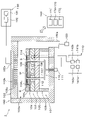
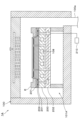
- FIGS. 1 and 2 are longitudinal sectional views showing the outline of the configuration of a processing module as a plasma processing apparatus according to the first embodiment. Note that FIGS. 1 and 2 show cross sections of different portions of a wafer support table, which will be described later.
- the processing module 1 in FIGS. 1 and 2 performs plasma processing such as etching and film formation on a wafer W as a substrate.
- the processing module 1 includes a plasma processing chamber 100 as a processing container, gas supply units 120 and 130, an RF (Radio Frequency) power supply unit 140, and an exhaust system 150. Further, the processing module 1 includes a wafer support table 101 and an upper electrode 102 as substrate supports.
- the wafer support table 101 is arranged in the lower region of the plasma processing space 100s in the plasma processing chamber 100 configured to be depressurized.
- Upper electrode 102 is arranged above wafer support 101 . Also, the top electrode 102 may function as part of the ceiling of the plasma processing chamber 100 .
- the wafer support 101 is configured to support the wafer W in the plasma processing space 100s.
- the wafer support 101 includes a lower electrode 103, an electrostatic chuck 104, an insulator 105, legs 106, and a lifter 107 is provided.
- the wafer support table 101 also includes a temperature adjustment unit configured to adjust the temperature of the electrostatic chuck 104 (for example, the temperature of the central upper surface 1041 ).
- the temperature adjuster includes, for example, heaters, channels, or a combination thereof.
- a temperature control fluid such as a refrigerant or a heat transfer gas flows through the flow path.
- the lower electrode 103 is made of a conductive material such as aluminum, and fixed to the insulator 105 .
- a flow path 108 for the temperature control fluid is formed, which constitutes a part of the temperature control section.
- a temperature control fluid is supplied to the flow path 108 from, for example, a chiller unit (not shown) provided outside the plasma processing chamber 100 .
- the temperature-controlled fluid supplied to the flow path 108 is returned to the chiller unit.
- the electrostatic chuck 104, the wafer W placed on the electrostatic chuck 104, and the edge ring E are cooled to a predetermined temperature by circulating low-temperature brine as a temperature control fluid in the flow path 108. can be done.
- the electrostatic chuck 104, the wafer W placed on the electrostatic chuck 104, and the edge ring E are heated to a predetermined temperature. can do.
- the electrostatic chuck 104 is a member configured to attract and hold the wafer W by electrostatic force, and is provided on the lower electrode 103 .
- the electrostatic chuck 104 is formed such that the upper surface of the central portion is higher than the upper surface of the peripheral portion.
- the upper surface 104 1 of the central portion of the electrostatic chuck 104 serves as a wafer mounting surface on which the wafer W is mounted, and the upper surface 104 2 of the peripheral portion of the electrostatic chuck 104 serves as a ring mounting surface on which the edge ring E is mounted. face.
- the edge ring E is an annular member arranged adjacent to the wafer W so as to surround the wafer W placed on the upper surface 1041 of the central portion of the electrostatic chuck 104 .
- the electrostatic chuck 104 is an example of a fixing portion that fixes the wafer W to the upper surface 104 1 at the center of the electrostatic chuck 104 , that is, the wafer mounting surface.
- An electrode 109 is provided in the center of the electrostatic chuck 104 .
- a DC voltage is applied to the electrode 109 from a DC power supply (not shown).
- the wafer W is attracted and held on the upper surface 1041 at the center of the electrostatic chuck 104 by the electrostatic force generated thereby.
- the electrostatic chuck 104 is configured to be able to attract and hold the edge ring E by electrostatic force, and is provided with an electrode (not shown) for holding the edge ring E on the wafer support 101 by electrostatic attraction.
- a heat transfer gas such as He gas is supplied to the upper surface 1042 of the peripheral portion of the electrostatic chuck 104 to the rear surface of the edge ring E placed on the upper surface 1042 .
- a feed hole (not shown) is formed.
- a heat transfer gas is supplied from a gas supply section (not shown) through the gas supply holes.
- a gas supply may include one or more gas sources and one or more pressure controllers.
- the gas supply is configured to supply heat transfer gas, for example from a gas source, to the gas supply holes via a pressure controller.
- the central portion of the electrostatic chuck 104 is formed, for example, to have a smaller diameter than the diameter of the wafer W, and the wafer W is placed on the upper surface (hereinafter referred to as wafer mounting surface) 104 1 of the central portion of the electrostatic chuck 104 .
- wafer mounting surface 104 1 of the central portion of the electrostatic chuck 104 .
- the peripheral edge of the wafer W protrudes from the central portion of the electrostatic chuck 104 .
- the edge ring E has, for example, a step formed in its upper portion, and the upper surface of the outer peripheral portion is formed higher than the upper surface of the inner peripheral portion.
- the inner peripheral portion of the edge ring E is formed so as to go under the peripheral portion of the wafer W projecting from the central portion of the electrostatic chuck 104 .
- a heater (specifically, a resistance heating element) forming part of the temperature control mechanism may be provided inside the electrostatic chuck 104.
- the electrostatic chuck 104 has, for example, a configuration in which a wafer attracting electrode 109 and an edge ring attracting electrode are sandwiched between insulating materials made of an insulating material, and a heater is embedded.
- the central portion of the electrostatic chuck 104 provided with the electrode 109 for attracting the wafer and the peripheral portion of the electrostatic chuck 104 provided with the electrode for attracting the edge ring may be integrally formed. , may be separate.
- the insulator 105 is a disk-shaped member made of ceramic or the like, to which the lower electrode 103 is fixed.
- the insulator 105 is formed to have the same diameter as the lower electrode 103, for example.
- the leg 106 is a cylindrical member made of ceramic or the like, and supports the electrostatic chuck 104 via the lower electrode 103 and insulator 105 .
- the legs 106 are formed, for example, to have an outer diameter equal to that of the insulator 105 and support the periphery of the insulator 105 .
- the lifter 107 is a lifting member that moves up and down with respect to the wafer mounting surface 1041 of the electrostatic chuck 104, and is formed in a columnar shape, for example.
- the lifter 107 can support the wafer W with its upper end protruding from the wafer mounting surface 1041 when lifted.
- the lifter 107 can transfer the wafer W between the electrostatic chuck 104 and an external transfer mechanism (not shown).
- Three or more lifters 107 are provided at intervals, and are provided so as to extend in the vertical direction.
- Each lifter 107 is connected to a support member 110 that supports the lifter 107 . Further, the support member 110 is connected to a drive unit 111 that generates driving force for raising and lowering the support member 110 and raises and lowers the plurality of lifters 107 .
- the drive unit 111 has, for example, a motor (not shown) as a drive source that generates the drive force.
- the lifter 107 is inserted through an insertion hole 112 whose upper end is open to the wafer mounting surface 1041 of the electrostatic chuck 104 .
- the insertion hole 112 is formed, for example, so as to penetrate the central portion of the electrostatic chuck 104 , the lower electrode 103 and the insulator 105 .
- the lifter 107 , the support member 110 and the drive unit 111 constitute an elevating mechanism for elevating the wafer W with respect to the wafer mounting surface 1041 .
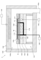
- a heat transfer medium composed of at least one of a liquid medium and a fluid solid medium is applied to the wafer mounting surface 104 1 via the wafer support table 101 .
- a heat transfer layer D is formed from the heat transfer medium.
- the wafer mounting surface 1041 of the electrostatic chuck 104 of the wafer support table 101 is formed with a supply port 113 for the heat transfer medium, as shown in FIG.
- a plurality of supply ports 113 are provided on the wafer mounting surface 1041 .
- a groove 114 may be provided on the wafer mounting surface 104 1 . The groove 114 is formed so that the heat transfer medium spreads along the wafer mounting surface 104 1 through the groove 114 .
- a channel 115 is provided, one end of which is in fluid communication with each of the supply ports 113. As shown in FIG. The other end of the channel 115 is fluidly connected to the gas supply section 120, for example.
- the channel 115 has, for example, a thin end portion (specifically, for example, a portion located inside the electrostatic chuck 104 ) on the wafer mounting surface 104 1 side. The medium is supplied to the wafer mounting surface 1041 through the supply port 113 by capillary action. Note that the channel 115 is formed, for example, across the electrostatic chuck 104 , the lower electrode 103 and the insulator 105 .
- the gas supply 120 may include one or more gas sources 121 and one or more flow controllers 122 .
- the gas supply unit 120 supplies, for example, one or more gases for generating the above-described heat transfer medium (hereinafter referred to as heat transfer medium generation gas) from the corresponding gas sources 121. They are configured to be supplied to the wafer support table 101 through corresponding flow controllers 122 .
- Each flow controller 122 may include, for example, a mass flow controller or a pressure-controlled flow controller.
- the gas supply 120 may include one or more flow modulation devices that modulate or pulse the flow of one or more heat transfer medium generating gases.
- the heat transfer medium generating gas supplied from the gas supply unit 120 is cooled in the flow path 115 by, for example, the lower electrode 103 cooled by the temperature control fluid in the flow path 108, and liquefied or solidified. It changes to a heat transfer medium composed of at least one of a medium and a fluid solid medium. "Liquid” includes sol and gel using a liquid as a dispersion medium. As described above, the heat transfer medium is supplied to the wafer mounting surface 1041 through the supply port 113 by, for example, capillary action to form the heat transfer layer D. As shown in FIG.
- the flow path 108 may function at least in part of a cooling mechanism configured to cool the heat transfer medium generating gas in the flow path 115 and transform it into a heat transfer medium, and the gas supply section 120 may serve as a wafer. It can function as at least a part of the heat transfer layer forming part configured to form the heat transfer layer D on the mounting surface 104 1 .
- the upper electrode 102 described above also functions as a shower head that supplies various gases from the gas supply unit 130 to the plasma processing space 100s.
- the top electrode 102 has a gas inlet 102a, a gas diffusion chamber 102b, and a plurality of gas inlets 102c.
- Gas inlet 102a is, for example, in fluid communication with gas supply 130 and gas diffusion chamber 102b.
- a plurality of gas inlets 102c are in fluid communication with the gas diffusion chamber 102b and the plasma processing space 100s.
- the upper electrode 102 is configured to supply various gases from the gas inlet 102a to the plasma processing space 100s through the gas diffusion chamber 102b and the plurality of gas inlets 102c.
- the gas supply 130 may include one or more gas sources 131 and one or more flow controllers 132 .
- gas supply 130 is configured, for example, to supply one or more process gases from respective gas sources 131 through respective flow controllers 132 to gas inlets 102a. be done.
- Each flow controller 132 may include, for example, a mass flow controller or a pressure-controlled flow controller.
- gas supply 130 may include one or more flow modulation devices that modulate or pulse the flow of one or more process gases.
- RF power supply 140 provides RF power, eg, one or more RF signals, to one or more electrodes, such as bottom electrode 103, top electrode 102, or both bottom electrode 103 and top electrode 102. configured to Thereby, plasma is generated from one or more processing gases supplied to the plasma processing space 100s. Accordingly, RF power supply 140 may function as at least part of a plasma generator configured to generate plasma from one or more process gases in plasma processing chamber 100 .
- the RF power supply unit 140 includes, for example, two RF generators 141a, 141b and two matching circuits 142a, 142b.
- RF power supply 140 is configured to supply a first RF signal from first RF generator 141a to bottom electrode 103 through first matching circuit 142a.
- the first RF signal may have a frequency within the range of 27MHz-100MHz.
- the RF power supply 140 is configured to supply a second RF signal from the second RF generator 141b to the lower electrode 103 via the second matching circuit 142b.
- the second RF signal may have a frequency within the range of 400 kHz to 13.56 MHz.
- a voltage pulse other than RF may be supplied instead of the second RF signal.
- the voltage pulse may be a negative DC voltage.
- the voltage pulse may be a triangular wave, an impulse.
- RF power supply 140 provides a first RF signal from an RF generator to bottom electrode 103, a second RF signal from another RF generator to bottom electrode 103, and A third RF signal may be configured to be supplied to the lower electrode 103 from yet another RF generator.
- a DC voltage may be applied to the top electrode 102 .
- the amplitude of one or more RF signals may be pulsed or modulated.
- Amplitude modulation may involve pulsing the RF signal amplitude between an on state and an off state, or between two or more different on states.
- the exhaust system 150 may be connected to an exhaust port 100e provided at the bottom of the plasma processing chamber 100, for example.
- Exhaust system 150 may include a pressure valve and a vacuum pump.
- Vacuum pumps may include turbomolecular pumps, roughing pumps, or combinations thereof.
- control unit 160 processes computer-executable instructions that cause processing module 1 to perform the various steps described in this disclosure. Controller 160 may be configured to control each of the other elements of processing module 1 to perform the various steps described herein. In one embodiment, part or all of the controller 160 may be included in other elements of the processing module 1 .
- Control unit 160 may include computer 170, for example.
- the computer 170 may include a processing unit (CPU: Central Processing Unit) 171, a storage unit 172, and a communication interface 173, for example.
- the processing unit 171 can be configured to perform various control operations based on programs stored in the storage unit 172 .
- the storage unit 172 may include RAM (Random Access Memory), ROM (Read Only Memory), HDD (Hard Disk Drive), SSD (Solid State Drive), or a combination thereof.
- the communication interface 173 may communicate with other elements of the processing module 1 via a communication line such as a LAN (Local Area Network).
- FIG. 3 is a flow chart for explaining an example of the above wafer processing.
- 4 to 7 are diagrams showing the state of the processing module 1 during the wafer processing. Note that the following processing is performed under the control of the control unit 160 .
- the wafer W is mounted on the wafer mounting surface 1041 of the wafer support table 101 (step S1). Specifically, the wafer W is loaded into the plasma processing chamber 100 by a transport mechanism (not shown) and placed on the wafer placement surface 104 1 of the electrostatic chuck 104 by raising and lowering the lifter 107 . . After that, the inside of the plasma processing chamber 100 is depressurized to a predetermined degree of vacuum (pressure p1) by the exhaust system 150 .
- pressure p1 a predetermined degree of vacuum
- a heat transfer medium composed of at least one of a liquid medium and a fluid solid medium is placed between the wafer mounting surface 104 1 and the wafer support table 101 . It is supplied between the back surface of the wafer W and the heat transfer layer D is formed (step S2).
- the wafer W is held on the wafer support table 101 .
- a DC voltage is applied to the electrode 109 of the electrostatic chuck 104, and the wafer W is electrostatically attracted to the electrostatic chuck 104 by electrostatic force.
- the temperature of the wafer mounting surface 1041 is adjusted to the temperature T1, and therefore the inside of the flow path 115 is also adjusted to the temperature T1.
- the temperature T1 is set to a temperature at which the process can be effectively performed, for example, equal to the temperature of the wafer mounting surface 1041 during the process.
- the heat transfer medium generating gas is supplied from the gas supply unit 120 to the flow path 115 of the wafer support 101 at a temperature T2 (>T1) and a pressure p2 (>p1). be.
- the heat transfer medium generating gas supplied to the flow path 115 is cooled to a temperature T1 in the flow path 115, and formed into a heat transfer medium composed of at least one of a liquid medium and a fluid solid medium. Become. Then, this heat transfer medium is supplied to the wafer mounting surface 1041 through the supply port 113 by, for example, capillary action.
- the heat transfer medium supplied to the wafer-mounting surface 104-1 spreads along the wafer-mounting surface 104-1 due to the capillary action caused by the gap between the wafer-mounting surface 104-1 and the back surface of the wafer W, thereby conducting heat transfer .
- Layer D is formed.
- the heat transfer layer D is deformable because it is made of a heat transfer medium that is composed of at least one of a liquid medium and a fluid solid medium.
- the gap between the wafer mounting surface 104-1 and the back surface of the wafer W is too narrow, the heat transfer medium will be moved along the wafer mounting surface 104-1 by capillary action due to the influence of the viscosity of the heat transfer medium. may not be able to spread out. Therefore, as described above, by providing the groove 114 in the wafer mounting surface 1041, the gap between the wafer mounting surface 1041 and the back surface of the wafer W can be widened. can be spread out appropriately along the wafer mounting surface 104 1 by . Further, a heat transfer medium having a low viscosity may be used so that the transfer of the heat transfer medium by capillarity is facilitated.
- the supply of the heat transfer medium to the wafer mounting surface 1041 (specifically, the supply of the heat transfer medium generating gas from the gas supply unit 120) is, for example, when the supply amount reaches a predetermined amount (specifically, is stopped when the supply time of the heat transfer medium generating gas from the gas supply unit 120 exceeds a predetermined time.
- monitoring means such as a camera is used to monitor leakage of the heat transfer medium from between the wafer mounting surface 1041 and the back surface of the wafer W, and when the leakage is monitored, the wafer is mounted.
- the supply of the heat transfer medium to the placement surface 104-1 may be stopped.
- the monitoring means such as a camera, is arranged, for example, outside the plasma processing chamber 100 and performs monitoring or imaging through an optical window provided in the plasma processing chamber 100 .
- step S3 plasma processing is performed on the wafer W on the wafer mounting surface 1041 on which the heat transfer layer D is formed. Specifically, the plasma processing is performed on the wafer W on which the heat transfer layer D is formed between the wafer mounting surface 1041 and the wafer W. As shown in FIG.
- the processing gas is supplied from the gas supply unit 130 to the plasma processing space 100s through the upper electrode 102 while the wafer W is continuously held on the wafer support table 101, for example.
- high-frequency power HF for plasma generation is supplied from the RF power supply unit 140 to the lower electrode 103 .
- the processing gas is excited and plasma P is generated.
- high-frequency power LF for attracting ions may be supplied from the RF power supply unit 140 .
- the plasma processing is applied to the wafer W by the action of the generated plasma P. As shown in FIG.
- the wafer mounting surface 1041 is adjusted to a predetermined temperature T1 by the temperature control fluid flowing through the flow path 108 in order to control the temperature of the wafer W.
- the lower surface, that is, the back surface, is in close contact with the heat transfer layer D.
- the heat transfer layer D is formed of a heat transfer medium, and since the heat transfer medium is composed of at least one of a liquid medium and a fluid solid medium, High thermal conductivity.
- the heat transfer layer D when the heat transfer layer D is used, compared to the conventional case where a heat transfer gas such as He flows between the wafer mounting surface 104 1 and the back surface of the wafer W, the heat transfer gas is transferred through the wafer mounting surface 104 1 . Therefore, the temperature of the wafer W can be efficiently adjusted. Specifically, even if a large amount of heat is input from the plasma P to the wafer W during plasma processing, the temperature of the wafer W can be kept constant through the temperature control of the wafer mounting surface 1041 . Further, when the set temperature of the wafer W is changed during plasma processing, the temperature of the wafer W can be immediately changed to the changed set temperature through the temperature control of the wafer mounting surface 1041. .
- the pressure p3 applied to the heat transfer layer D during plasma processing is 0.1 Torr to 100 Torr, including the pressure applied to the heat transfer layer D by electrostatically attracting the wafer W.
- a DC voltage may be applied to the electrode for attracting the edge ring of the electrostatic chuck 104 so that the edge ring E may be electrostatically attracted to the electrostatic chuck 104 .
- a heat transfer gas may be supplied toward the back surface of the edge ring E from gas supply holes (not shown) formed in the top surface 1042 of the peripheral portion of the electrostatic chuck 104 .
- the supply of high-frequency power HF from the RF power supply unit 140 and the supply of processing gas from the gas supply unit 130 are stopped. If the high-frequency power LF is being supplied during the plasma processing, the supply of the high-frequency power LF is also stopped. Also, the inside of the plasma processing chamber 100 is depressurized to a predetermined degree of vacuum (pressure p1) by the exhaust system 150 .
- the pressure p1 is, for example, less than 0.001 Torr. If the electrostatic chuck 104 is sucking and holding the edge ring E and supplying the heat transfer gas to the back surface of the edge ring E during plasma processing, at least one of these is stopped. You may do so.
- the wafer W is separated from the wafer mounting surface 1041 , and the heat transfer layer D is vaporized and removed (step S4).
- the heat transfer layer D is removed by vaporization.
- the wafer W is lifted by the lifter 107, and as shown in FIG. , is separated from the wafer mounting surface 104 1 .
- the heat transfer layer D is exposed to a reduced pressure atmosphere, specifically an atmosphere with a pressure p1 of less than 0.001 Torr, whereby it is vaporized and removed.
- the heat transfer medium forming the heat transfer layer D is a liquid or a fluid solid at a temperature T1 at a pressure p3 of 0.1 to 100 Torr and less than 0.001 Torr. is used at a pressure p1 which is gaseous at temperature T1.
- the heat transfer medium generating gas for generating the heat transfer medium forming the heat transfer layer D includes, for example, at least one of B (boron) and C (carbon), which are constituent atoms of the heat transfer layer D, At least one of H (hydrogen), N (nitrogen), and O (oxygen) constituting gas components is included. Furthermore, the heat transfer medium generating gas preferably consists of components that do not interfere with the plasma processing.
- the removal of the heat transfer layer D from the wafer mounting surface 104E1 includes at least one of exposing the heat transfer layer D to plasma, heating the heat transfer layer D, and irradiating the heat transfer layer D with light. It may be used in place of or in combination with exposing the heat transfer layer D to the reduced pressure atmosphere.
- the wafer W is unloaded (step S5). Specifically, the wafer W is transferred from the lifter 107 to a transport mechanism (not shown) and unloaded from the plasma processing chamber 100 by the transport mechanism. This completes a series of wafer processing.
- a heat transfer medium composed of at least one of a liquid medium and a fluid solid medium is placed on the wafer through the wafer support table 101 during plasma processing.
- a heat transfer layer D is formed between the surface 1041 and the back surface of the wafer W. Since the heat transfer layer D is made of the heat transfer medium as described above, it has a higher thermal conductivity than the heat transfer layer made of heat transfer gas. Further, since the heat transfer layer D is deformable as described above, it can be brought into close contact with the lower surface of the wafer W. As shown in FIG. Therefore, according to this embodiment, heat can be efficiently exchanged between the wafer W and the wafer mounting surface 1041 via the heat transfer layer D.
- the temperature of the wafer W can be efficiently adjusted via the wafer mounting surface 1041 during plasma processing.
- the wafer mounting surface 104-1 can efficiently absorb heat from the wafer W through the heat transfer layer D, and the wafer mounting surface 104-1 can absorb heat through the heat transfer layer D. can heat the wafer W efficiently.
- the heat transfer medium forming the heat transfer layer D is composed of a liquid or a fluid solid, clogging of the flow path 115 by the heat transfer medium can be suppressed. can. Further, since the heat transfer layer D is vaporized and removed when the wafer W is separated from the wafer mounting surface 1041 , there is no need to provide a separate step for removing the heat transfer layer D. FIG. Therefore, throughput can be improved.
- the wafer W is attracted and held on the wafer mounting surface 104 1 by the electrostatic force of the electrostatic chuck 104 during plasma processing or the like.
- the heat transfer layer D and the lower surface of the wafer W can be brought into closer contact with each other, so that the heat removal efficiency from the wafer W via the wafer mounting surface 1041 and the heat transfer layer D or the heating efficiency of the wafer W can be further improved. can be improved.
- the heat transfer layer D and the lower surface of the wafer W can be brought into close contact with each other by attraction and holding by the electrostatic chuck 104 as described above. Therefore, even if the wafer W is warped, the heat can be removed from the wafer W or the wafer W can be heated efficiently.
- FIG. 8 is a diagram for explaining another example of the form of supply of the heat transfer medium.
- the heat transfer medium generating gas is supplied to the wafer support 101 from the outside and changed to the heat transfer medium within the wafer support 101.
- the heat transfer medium itself may be supplied from the medium supply unit 180 to the wafer support 101 (specifically, the flow path 115).
- the media supply 180 may include one or more sources 181 of heat transfer media and one or more flow controllers 182 .
- media supply 180 supplies, for example, one or more heat transfer media from respective sources 181 through respective flow controllers 182 to wafer support 101 . Configured.
- media supply 180 may include one or more flow modulation devices that modulate or pulse the flow of one or more heat transfer media.
- the heat transfer medium in the wafer support table 101 is supplied to the wafer mounting surface 1041 by capillarity.
- the wafer of the heat transfer medium in the wafer support 101 is controlled by the supply pressure of the heat transfer medium generating gas to the wafer support 101 from the outside or the supply pressure of the heat transfer medium to the wafer support 101 from the outside. Supply to the mounting surface 104-1 may also be performed.
- the heat transfer medium in the wafer support table 101 is supplied to the wafer mounting surface 1041 by the supply pressure of the heat transfer medium to the wafer support table 101 from the outside, the heat transfer medium is as follows. You can use things. That is, a heat transfer medium mixed with powder having higher thermal conductivity than the base material of the heat transfer medium may be used. Specifically, the powder having higher thermal conductivity than the base material of the heat transfer medium is, for example, carbon nanotube powder.
- the thermal conductivity is A mist containing high powders may be used as the heat transfer medium generating gas.
- the heat transfer medium can be changed into a heat transfer medium mixed with powder having high thermal conductivity .
- FIG. 9 and 10 are diagrams showing specific examples of the groove 114.
- FIG. A plurality of support columns 116 for supporting the back surface of the wafer W may be formed on the wafer mounting surface 1041 of the electrostatic chuck 104, as shown in FIG .
- recesses formed between support posts 116 constitute grooves 114 .
- a porous body (specifically, for example, porous ceramics) 117 may be arranged in the groove 114 to fill the groove 114 .
- the wafer mounting surface may be made of a porous material at portions other than the grooves 114 (specifically, for example, the tops of the support columns 116). Moreover, when the groove 114 is not provided on the wafer mounting surface, the entire surface of the wafer mounting surface may be formed of a porous material.
- the heat transfer layer D is formed on the entire wafer mounting surface 104-1 including, for example, the central region and the peripheral region of the wafer mounting surface 104-1 .
- the heat transfer layer D may be formed only in the region of the part.
- the heat transfer layer D may be formed only in the central region of the wafer mounting surface 1041 facing the central portion of the wafer W.
- the heat transfer layer D is formed only in the peripheral area of the wafer mounting surface 1041 facing the peripheral edge of the wafer W. good too.
- the heat transfer layer D can be formed only in the partial area. .
- the heat transfer layer D has a uniform thickness over the entire wafer mounting surface 104-1 including, for example, the central region and the peripheral region of the wafer mounting surface 104-1 .
- the thickness may differ within the wafer mounting surface 104-1 .
- the heat transfer layer D is formed more in the central region of the wafer mounting surface 1041 facing the central portion of the wafer W than in the peripheral region. You can make it thinner.
- the peripheral edge region of the wafer mounting surface 1041 facing the peripheral edge of the wafer W has a higher heat transfer layer thickness than the central region.
- the heat transfer layer D may be thinned. In this way, by thinning the heat transfer layer D only in a partial region such as the central region of the wafer mounting surface 104-1 , the heat exchange efficiency between the wafer mounting surface 104-1 and the wafer W can be reduced. The heat exchange efficiency can be increased only in the partial area.
- the depth of the grooves 114 is made different for each region on the wafer mounting surface 104-1 , so that only a part of the regions such as the central region can transmit. Thermal layer D can be made thinner.
- the thickness of the porous material is made different for each region of the wafer mounting surface 104-1 , whereby the wafer can be mounted.
- the heat exchange efficiency between the wafer mounting surface 104-1 and the wafer W can be varied within the plane in the same manner as when the depth of the grooves 114 is varied for each region on the mounting surface 104-1 .
- the heat transfer layer D is formed by mixing a high thermal conductivity conductive medium and a low thermal conductive medium. Different mixing ratios of the modulus conducting media may be used. This also makes it possible to vary the heat exchange efficiency between the wafer mounting surface 1041 and the wafer W within the surface.
- the density of the grooves 114 may be varied for each region on the wafer mounting surface 1041 .
- the density of support columns 116 may be varied for each region on wafer mounting surface 1041 .
- the ratio of the portion where the heat transfer layer is formed can be made different for each region on the wafer mounting surface 104-1 , and the heat exchange efficiency between the wafer mounting surface 104-1 and the wafer W can be changed in-plane. can be different.
- the heat transfer layer D may have electrical insulation. As a result, a residual charge is generated in the heat transfer layer D, and the residual charge can be used for electrostatic attraction of the wafer W.
- FIG. Moreover, the heat transfer layer D may have conductivity. As a result, residual charges generated on the wafer W through the heat transfer layer D can be removed.
- the heat transfer layer D may be configured by wrapping a conductive portion with an electrically insulating portion. As a result, high thermal conductivity is ensured in the electrically conductive portion (generally, the higher the electrical conductivity, the higher the thermal conductivity), and the electrically insulating portion allows the residual charge generated in the portion to cool the wafer W. The can be electrostatically adsorbed.
- the wafer mounting surface 1041 of the wafer support table 101 may have a constant height in the central region and the peripheral region, that is, may be macroscopically flat, or may be high in the central region. Alternatively, the peripheral region may be elevated.
- a wafer W having a temperature higher than that of the wafer mounting surface 104-1 is mounted on the wafer mounting surface 104-1 , and the wafer W is , the wafer W and the wafer mounting surface 1041 can be brought into close contact with each other when the rear surface is cooled and thermally deformed into a convex shape.
- the wafer mounting surface 104-1 is formed in a concave shape with a low central region, a wafer W having a temperature lower than that of the wafer mounting surface 104-1 is mounted on the wafer mounting surface 104-1 , and the wafer W
- the wafer W and the wafer mounting surface 1041 can be brought into close contact with each other when the back surface is heated and thermally deformed into a concave shape.
- the heat transfer layer D may be formed on the entire wafer mounting surface 104-1 , or may be formed on part of the wafer mounting surface 104-1 (specifically, for example, the central region or the peripheral region). either one).
- a heat transfer gas such as He gas may be supplied to a region of the wafer mounting surface 1041 where the heat transfer layer D is not formed.
- the electrostatic chuck 104 that attracts and holds the wafer W by electrostatic force generated by applying a DC voltage to the internal electrode 109 serves as a fixing portion that holds or fixes the wafer W on the wafer mounting surface 1041.
- the fixing portion for electrically holding or fixing the wafer W is not limited to holding by electrostatic force, but may be holding by Johnsen-Rahbek force.
- the fixing portion is not limited to the one that holds electrically as described above.
- the fixing part may be a physical fixing part such as a clamp.
- the clamp is to fix the wafer W by sandwiching the wafer W between the clamp and the wafer support 101 . Note that the fixing portion may be omitted.
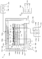
- FIG. 11 is a plan view schematically showing the configuration of a plasma processing system including processing modules as a plasma processing apparatus according to the second embodiment.
- the atmospheric part 10 includes an atmospheric module that performs desired processing on a wafer W as a substrate under atmospheric pressure.
- the decompression unit 11 includes a processing module 1A that performs desired processing on the wafer W under a decompressed atmosphere (vacuum atmosphere).
- the load lock modules 20 and 21 are provided to connect the loader module 30 included in the atmosphere section 10 and the transfer module 50 included in the decompression section 11 via gate valves (not shown).
- the load lock modules 20, 21 are configured to hold the wafer W temporarily. Further, the load lock modules 20 and 21 are configured so that the inside can be switched between an atmospheric pressure atmosphere and a reduced pressure atmosphere.
- the atmospheric part 10 has a loader module 30 having a transport mechanism 40, which will be described later, and a load port 32 on which a FOUP (FOUP: Front Opening Unified Pod) 31 is placed.
- the FOUP 31 is capable of storing a plurality of wafers W.
- FIG. An orienter module (not shown) for adjusting the horizontal direction of the wafer W, a buffer module (not shown) for temporarily storing a plurality of wafers W, and the like are connected to the loader module 30. good.
- the loader module 30 has a rectangular housing, and the inside of the housing is maintained at atmospheric pressure.
- a plurality of, for example, five load ports 32 are arranged side by side on one side surface that constitutes the long side of the housing of the loader module 30 .
- Load-lock modules 20 and 21 are arranged side by side on the other side surface constituting the long side of the housing of the loader module 30 .
- a transport mechanism 40 capable of transporting the wafer W is provided inside the housing of the loader module 30 .
- the transfer mechanism 40 has a transfer arm 41 that supports the wafer W during transfer, a turntable 42 that rotatably supports the transfer arm 41, and a base 43 on which the turntable 42 is mounted.
- a guide rail 44 extending in the longitudinal direction of the loader module 30 is provided inside the loader module 30 .
- the base 43 is provided on guide rails 44 , and the transport mechanism 40 is configured to be movable along the guide rails 44 .
- the decompression unit 11 accommodates a transfer module 50 for transferring the wafer W and the edge ring E, a processing module 1A as a plasma processing apparatus for performing plasma processing on the wafer W transferred from the transfer module 50, and the edge ring E. It has a storage module 60 as a storage section.
- the interiors of the transfer module 50 and the processing module 1 (specifically, the interiors of the decompression transfer chamber 51 and the plasma processing chamber 100, which will be described later) are each maintained in a reduced pressure atmosphere, and the interior of the storage module 60 is also maintained in a reduced pressure atmosphere.
- a plurality of processing modules 1A for example six, are provided, and a plurality of storage modules 60, for example two, are provided.
- the transfer module 50 includes a reduced pressure transfer chamber 51 having a polygonal (pentagonal in the illustrated example) housing, and the reduced pressure transfer chamber 51 is connected to the load lock modules 20 and 21 .
- the transfer module 50 transfers the wafer W loaded into the load lock module 20 to one of the processing modules 1A, and transfers the wafer W, which has undergone desired plasma processing in the processing module 1A, through the load lock module 21. It is carried out to the atmospheric part 10 .
- the transfer module 50 transfers the edge ring E in the storage module 60 to one of the processing modules 1A and unloads the edge ring E to be replaced in the processing module 1A to the storage module 60 .
- the processing module 1A is connected to the transfer module 50 via the gate valve 61.
- the difference between the processing module 1A and the processing module 1 described with reference to FIG. 1 etc. will be described later.
- the storage module 60 is connected to the transfer module 50 via a gate valve 62.
- a transfer mechanism 70 configured to transfer the wafer W and the edge ring E is provided inside the reduced-pressure transfer chamber 51 of the transfer module 50 .
- the transfer mechanism 70 like the transfer mechanism 40 described above, includes a transfer arm 71 that supports the wafer W and the edge ring E during transfer, a turntable 72 that rotatably supports the transfer arm 71, and a base on which the turntable 72 is mounted. a platform 73;
- a guide rail 74 extending in the longitudinal direction of the transfer module 50 is provided inside the reduced-pressure transfer chamber 51 of the transfer module 50 .
- the base 73 is provided on guide rails 74 , and the transport mechanism 70 is configured to be movable along the guide rails 74 .
- the transfer arm 71 receives the wafer W held in the load lock module 20 and carries it into the processing module 1A. Also, the transfer arm 71 receives the wafer W held in the processing module 1A and unloads it to the load lock module 21 . Further, in the transfer module 50, the transfer arm 71 receives the edge ring E in the storage module 60 and carries it into the processing module 1A. Further, the transport arm 71 receives the edge ring E held in the processing module 1A and transports it to the storage module 60. FIG.
- controller 80 processes computer-executable instructions that cause plasma processing system PS to perform various operations described in this disclosure. Controller 80 may be configured to control each of the other elements of plasma processing system PS to perform the various processes described herein. In one embodiment, part or all of controller 80 may be included in other elements of plasma processing system PS. In one embodiment, controller 80 also processes computer-executable instructions that cause processing module 1A to perform various steps described in this disclosure. Controller 80 may be configured to control each of the other elements of processing module 1A to perform the various steps described herein. In one embodiment, part or all of the controller 80 may be included in other elements of the processing module 1A. The controller 80 may include a computer 90, for example.
- the computer 90 may include a processing unit (CPU) 91, a storage unit 92, and a communication interface 93, for example.
- the processing unit 91 can be configured to perform various control operations based on programs stored in the storage unit 92 .
- Storage unit 92 may include RAM, ROM, HDD, SSD, or a combination thereof.
- the communication interface 93 may communicate with other elements of the plasma processing system PS via a communication line such as LAN.
- the wafer W is taken out from the desired FOUP 31 and loaded into the load lock module 20 by the transport mechanism 40 . After that, the inside of the load lock module 20 is sealed and the pressure is reduced. After that, the inside of the load lock module 20 and the inside of the transfer module 50 are communicated.
- the wafer W is held by the transport mechanism 70 and transported from the load lock module 20 to the transfer module 50 .
- the gate valve 61 is opened, and the wafer W is carried into the desired processing module 1A by the transfer mechanism 70. After that, the gate valve 61 is closed, and the desired processing is performed on the wafer W in the processing module 1A. The processing performed on the wafer W in this processing module 1A will be described later.
- the gate valve 61 is opened, and the transfer mechanism 70 unloads the wafer W from the processing module 1A. After that, the gate valve 61 is closed.
- the wafer W is loaded into the load lock module 21 by the transport mechanism 70 .
- the inside of the load lock module 21 is sealed and opened to the atmosphere. After that, the inside of the load lock module 21 and the inside of the loader module 30 are communicated with each other.
- the wafer W is held by the transfer mechanism 40 and returned from the load lock module 21 via the loader module 30 to the desired FOUP 31 to be accommodated. This completes a series of wafer processing in the plasma processing system PS.
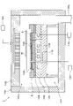
- FIGS. 12 and 13 are longitudinal sectional views showing the outline of the configuration of the processing module 1A. Note that FIGS. 12 and 13 show cross sections of different portions of the wafer support table 101A.
- the wafer W is the object whose temperature is adjusted via the heat transfer layer D formed by the wafer support 101 and the heat transfer medium.
- the processing module 1A of FIGS. 12 and 13 differs from the processing module 1 of FIGS. 1 and 2 mainly in the configuration of the wafer support. This difference will be mainly described below.
- a wafer support table 101A of the processing module 1A includes, for example, a lower electrode 200, an electrostatic chuck 201, an insulator 202 and legs 106, and a lifter 107 and a lifter 203 are provided.
- the electrostatic chuck 201 has a wafer mounting surface 104 1 in the central portion, and a top surface 201 1 of the peripheral portion serves as a ring mounting surface on which the edge ring E is mounted. Become.
- the electrostatic chuck 201 is an example of a fixing portion that fixes the edge ring E to the upper surface 2011 of the peripheral portion of the electrostatic chuck 201, that is, the ring mounting surface.
- the electrostatic chuck 201 is provided with an electrode 109 for holding the wafer W by electrostatic attraction in the center, and an electrode 204 for holding the edge ring E by electrostatic attraction at the periphery.
- a DC voltage is applied to the electrode 204 from a DC power supply (not shown). Due to the electrostatic force generated thereby, the edge ring E is attracted and held on the upper surface (hereinafter referred to as ring mounting surface) 2011 of the peripheral portion of the electrostatic chuck 201 .
- the electrodes 204 are, for example, bipolar, including a pair of electrodes, but may also be unipolar.
- the lifter 203 is a lifting member that moves up and down with respect to the ring mounting surface 2011 of the electrostatic chuck 201, and is formed in a columnar shape, for example.
- the lifter 203 can support the edge ring E with its upper end protruding from the ring mounting surface 2011 when lifted.
- the edge ring E can be transferred between the electrostatic chuck 201 and the transport arm 71 of the transport mechanism 70 by the lifter 203 .
- Three or more lifters 203 are provided at intervals along the circumferential direction of the electrostatic chuck 201 . Also, the lifter 203 is provided so as to extend in the vertical direction.
- the lifter 203 is connected to a drive section 205 that moves the lifter 203 up and down.
- the drive unit 205 is provided for each lifter 203, for example. Further, the drive unit 205 has, for example, a motor (not shown) as a drive source that generates a driving force for raising and lowering the lifter 203 .
- the lifter 203 is inserted through an insertion hole 206 whose upper end is open to the ring mounting surface 2011 of the electrostatic chuck 201 .
- the insertion hole 206 is formed, for example, so as to penetrate the peripheral portion of the electrostatic chuck 201 , the lower electrode 200 and the insulator 202 .
- a heat transfer medium supply port 207 is formed on the ring mounting surface 2011 of the electrostatic chuck 201 of the wafer support table 101A.
- a plurality of supply ports 207 are provided on the ring mounting surface 2011 .
- a groove 208 may be provided on the ring mounting surface 2011 . The groove 208 is formed so that the heat transfer medium spreads along the ring mounting surface 201 - 1 through the groove 208 .
- a channel 209 is provided, one end of which is in fluid communication with each of the supply ports 207 .
- the other end of the channel 209 is fluidly connected to a gas supply section 210, for example.
- the channel 209 has, for example, a narrow end portion (specifically, for example, a portion located in the electrostatic chuck 201) on the ring mounting surface 2011 side, and the heat transfer in the channel 209 is reduced.
- the medium is supplied to the ring mounting surface 2011 through the supply port 207 by capillarity.
- the channel 209 is formed, for example, across the electrostatic chuck 201 , the lower electrode 200 and the insulator 202 .
- the gas supply 210 may include one or more gas sources 211 and one or more flow controllers 212 .
- the gas supply unit 210 supplies one or more heat transfer medium generating gases from respective gas sources 211 to the wafer support 101A via respective flow controllers 212.
- Each flow controller 212 may include, for example, a mass flow controller or a pressure-controlled flow controller.
- the gas supply 210 may include one or more flow modulation devices that modulate or pulse the flow of one or more heat transfer medium generating gases.
- the heat transfer medium generating gas supplied from the gas supply unit 210 is cooled in the flow path 209 by, for example, the lower electrode 200 cooled by the temperature control fluid in the flow path 108, and liquefied or solidified. It changes to a heat transfer medium composed of at least one of a medium and a fluid solid medium. As described above, the heat transfer medium is supplied to the ring mounting surface 2011 through the supply port 207 by capillary action, for example, to form the heat transfer layer DA.
- the flow path 108 may function at least in part of a cooling mechanism configured to cool and transform the heat transfer medium generating gas within the flow path 209 into a heat transfer medium
- the gas supply section 210 may function as a ring It can function as at least a part of the heat transfer layer forming part configured to form the heat transfer layer DA on the mounting surface 201-1 .
- FIG. 14 is a flow chart for explaining an example of the above wafer processing.
- 15 to 17 are diagrams showing the state of the processing module 1A during the wafer processing. Note that the following processing is performed under the control of the control unit 160 .
- the edge ring E is mounted on the ring mounting surface 2011 of the wafer support table 101A (step S11). Specifically, the edge ring E is carried into the plasma processing chamber 100 by the transport mechanism 70 and is mounted on the ring mounting surface 2011 of the electrostatic chuck 201 by raising and lowering the lifter 203 . After that, the inside of the plasma processing chamber 100 is decompressed to a predetermined degree of vacuum (pressure p11) by the exhaust system 150 .
- pressure p11 a predetermined degree of vacuum
- the edge ring E is transported into the plasma processing chamber 100, for example, as follows. That is, first, the edge ring E inside the storage module 60 is held by the transfer arm 71 of the transfer mechanism 70 . Next, the transfer arm 71 holding the edge ring E is inserted into the plasma processing chamber 100 of the processing module 1A through a loading/unloading port (not shown). Then, the edge ring E is transported by the transport arm 71 above the ring mounting surface 2011 of the electrostatic chuck 201 . After that, the lifter 203 is lifted and the transfer arm 71 is pulled out from the plasma processing chamber 100 , whereby the edge ring E is mounted on the ring mounting surface 2011 of the electrostatic chuck 201 .
- a heat transfer medium composed of at least one of a liquid medium and a fluid solid medium is placed between the ring mounting surface 2011 and the wafer support table 101A. It is supplied between the back surface of the edge ring E and the heat transfer layer DA is formed (step S12).
- the edge ring E is held by the wafer support 101A.
- a DC voltage is applied to the electrode 204 of the electrostatic chuck 201, and the edge ring E is electrostatically attracted to the electrostatic chuck 201 by electrostatic force.
- the temperature of the ring mounting surface 2011 is adjusted to the temperature T11, and therefore the inside of the flow path 209 is also adjusted to the temperature T11.
- the temperature T11 is set to a temperature at which process treatment can be effectively performed, for example, equal to the temperature of the ring mounting surface 2011 during process treatment.
- the heat transfer medium generating gas is supplied from the gas supply unit 210 to the flow path 209 of the wafer support 101A at a temperature T12 (>T11) and a pressure p12 (>p11). be done.
- the heat transfer medium generating gas supplied to the flow path 209 is cooled to a temperature T11 in the flow path 209, and formed into a heat transfer medium composed of at least one of a liquid medium and a fluid solid medium. Become. Then, this heat transfer medium is supplied to the ring mounting surface 2011 through the supply port 207 by capillary action, for example.
- the heat transfer medium supplied to the ring-mounting surface 201-1 spreads along the ring-mounting surface 201-1 due to the capillary action caused by the gap between the ring-mounting surface 201-1 and the back surface of the edge ring E, and the heat transfer medium spreads along the ring-mounting surface 201-1 .
- a thermal layer DA is formed.
- the heat transfer layer DA is deformable like the heat transfer layer D described above.
- the gap between the ring mounting surface 201-1 and the back surface of the edge ring E can be widened, and the heat transfer medium can be displaced by capillary action. can be appropriately spread along the ring mounting surface 201-1 .
- the pressure p13 applied to the heat transfer layer DA is 0.1 Torr to 100 Torr, including the pressure applied to the heat transfer layer DA by electrostatically attracting the edge ring E.
- the supply of the heat transfer medium to the ring mounting surface 201-1 (specifically, the supply of the heat transfer medium generating gas from the gas supply unit 210) is, for example, when the supply amount reaches a predetermined amount (specifically, is stopped when the supply time of the heat transfer medium generating gas from the gas supply unit 210 exceeds a predetermined time.
- monitoring means such as a camera is used to monitor leakage of the heat transfer medium from between the ring mounting surface 2011 and the back surface of the edge ring E, and when leakage is monitored, the ring The supply of the heat transfer medium to the mounting surface 2011 may be stopped.
- plasma processing is performed on the wafer W on the upper surface of the electrostatic chuck 201 on which the heat transfer layer DA is formed, that is, the mounting surface (step S13).
- plasma processing is performed in the same manner as the processing described with reference to FIG. 3 and the like. More specifically, for example, the wafer W is mounted on the wafer mounting surface 104-1 of the wafer support table 101A, and the heat transfer layer D is formed between the wafer mounting surface 104-1 and the back surface of the wafer W. After that, the wafer W is subjected to plasma processing. After that, the heat transfer layer D is vaporized and removed, and the wafer W is unloaded.
- the ring mounting surface 2011 is adjusted to a predetermined temperature T11 by the temperature control fluid flowing through the channel 108 in order to control the temperature of the edge ring E.
- the heat transfer layer DA is formed of a heat transfer medium, and since the heat transfer medium is composed of at least one of a liquid medium and a fluid solid medium, High thermal conductivity.
- the edge is The temperature of the ring E can be adjusted efficiently. Specifically, even if a large amount of heat is input from the plasma P to the edge ring E during plasma processing, the temperature of the edge ring E can be maintained constant through the temperature control of the ring mounting surface 2011 . . Further, when the set temperature of the edge ring E is changed during plasma processing, the temperature of the edge ring E can be immediately changed to the changed set temperature through the temperature control of the ring mounting surface 2011 . can be done.
- a DC voltage is applied to the electrode 204 of the electrostatic chuck 201 even during plasma processing, whereby the edge ring E is electrostatically attracted to and held by the electrostatic chuck 201 .
- the degree of close contact of the edge ring E with the wafer support 101A may be controlled by electrostatic force to control heat removal from the edge ring E by the wafer support 101A.
- the edge ring E is separated from the ring mounting surface 2011 , and the heat transfer layer DA is vaporized and removed (step S14).
- the heat transfer layer DA is removed by vaporization. The separation of the edge ring E from the ring mounting surface 2011 , that is, the removal of the edge ring E does not need to be performed each time the wafer W is subjected to plasma processing. Done when damaged or consumed by plasma.
- the edge ring E is lifted by the lifter 203, As shown in FIG. 16, it is spaced apart from the ring mounting surface 2011 .
- the heat transfer layer DA is exposed to a reduced pressure atmosphere, specifically an atmosphere with a pressure p11 of less than 0.001 Torr, whereby it is vaporized and removed.
- the removal of the heat transfer layer DA from the ring mounting surface 2011 includes at least one of exposing the heat transfer layer DA to plasma, heating the heat transfer layer DA, and irradiating the heat transfer layer DA with light. , may be used in place of or in combination with exposing the heat transfer layer DA to a reduced pressure atmosphere.
- the heat transfer medium generating gas for the heat transfer layer DA may be the same as or different from that for the heat transfer layer D.
- the edge ring E is carried out (step S15). Specifically, the edge ring E is transferred from the lifter 203 to the transport mechanism 70 and carried out of the plasma processing chamber 100 by the transport mechanism 70 . This completes a series of wafer processing.
- the heat transfer medium composed of at least one of the liquid medium and the fluid solid medium is placed between the ring mounting surface 2011 and the wafer support 101A. It is supplied between the back surface of the edge ring E and forms a heat transfer layer DA. Therefore, in this embodiment, for the same reason as in the first embodiment, the temperature of the edge ring E can be efficiently adjusted via the ring mounting surface 2011 during plasma processing. Further, clogging of the flow path 209 by the heat transfer medium can be suppressed. Furthermore, since it is not necessary to separately provide a step of removing the heat transfer layer DA, the throughput can be improved.
- the edge ring E is attracted and held on the ring mounting surface 2011 by the electrostatic force of the electrostatic chuck 201 during plasma processing or the like.
- the heat transfer layer DA and the lower surface of the edge ring E can be brought into closer contact with each other. Efficiency can be further improved.
- the wafer W is the object whose temperature is adjusted via the heat transfer layer D formed of the wafer support 101 and the heat transfer medium.
- both the wafer W and the edge ring E are subject to temperature adjustment.
- only the edge ring E may be subject to temperature adjustment.
- the processing module 1A in the examples of FIGS. both of the configurations such as the flow path 115 for forming are provided, the latter configuration may be omitted.
- the temperature is adjusted for both the wafer W and the edge ring E, and the timing for forming the heat transfer layer D for the wafer W is the timing for forming the heat transfer layer DA for the edge ring E. was different from, but may be the same. By making them the same, the throughput can be improved.
- the supply form of the heat transfer medium for forming the heat transfer layer DA for the edge ring E is not limited to the above example, and the heat transfer medium for forming the heat transfer layer D for the wafer W described above is Variations similar to the supply form can be applied.
- the heat transfer medium for forming the heat transfer layer DA for the edge ring E is not limited to the above example, and the heat transfer medium for forming the heat transfer layer D for the wafer W described above may be modified in the same manner. Examples can be applied.
- the groove 208 for forming the heat transfer layer DA for the edge ring E can be applied to the same specific example as the groove 114 for forming the heat transfer layer DA for the edge ring E described above. .
- the ring mounting surface may be formed of a porous body in a portion other than the grooves 208 (specifically, for example, the tops of the support columns provided in the grooves 208), similarly to the wafer mounting surface.
- the entire surface of the ring mounting surface may be made of a porous material.
- the heat transfer layer DA for the edge ring E may be formed on the entire ring mounting surface 201-1 , similarly to the heat transfer layer D for the wafer W, or may be formed on a part of the ring mounting surface 201-1 .
- a heat transfer layer may be formed only in the region.
- the heat transfer layer DA may be formed only on the inner peripheral side of the ring mounting surface 201-1 , or may be formed only on the outer peripheral side of the ring mounting surface 201-1 .
- the heat transfer layer DA for the edge ring E may have different thicknesses within the ring mounting surface 2011 , similarly to the heat transfer layer D for the wafer W.
- the heat transfer layer DA may be thinner than on the outer peripheral side, and on the outer peripheral side of the ring mounting surface 201-1 , compared to the inner peripheral side, The heat transfer layer DA may be thin.
- the thickness of the porous material may be varied for each region of the ring mounting surface 201-1 .
- the heat transfer layer DA for the edge ring E is formed by mixing a high thermal conductivity conductive medium and a low thermal conductive medium.
- the mixing ratio of the conductive medium and the low thermal conductivity conductive medium may be different.
- the density of the grooves 208 may be varied for each region on the ring mounting surface 2011 .
- the heat transfer layer DA for the edge ring E may be electrically insulating. Moreover, the heat transfer layer DA may have conductivity. Furthermore, the heat transfer layer DA may be configured by wrapping a conductive portion with an electrically insulating portion.
- the heat transfer layer DA may be formed on the entire ring mounting surface 201-1 , or may be formed only on a part of the ring mounting surface 201-1 .
- a heat transfer gas such as He gas may be supplied to a region of the ring mounting surface 2011 where the heat transfer layer DA is not formed.
- the electrostatic chuck 201 attracts and holds the edge ring E by electrostatic force generated by applying a DC voltage to the internal electrode 204 as a fixing portion for holding or fixing the edge ring E to the ring mounting surface 201 1 .
- the electrically fixed portion is not limited to holding by electrostatic force, and may be held by Johnsen-Rahbek force.
- the fixing portion is not limited to the one that holds electrically as described above.
- the fixing part may be a physical fixing part such as a clamp. Note that the fixing portion may be omitted.
- the edge ring E was stored in the storage module 60 connected to the transfer module 50. good.
- plasma etching is performed as plasma processing, but the technology of the present disclosure can also be applied to the case of performing processing other than etching (for example, film formation processing) as plasma processing.
- a cover ring arranged to cover the outer surface of the edge ring is placed on the wafer support of the processing module that performs plasma processing.
- a heat transfer medium is supplied between the mounting surface of the wafer support table on which the cover ring is mounted and the bottom surface of the cover ring. , a heat transfer layer may be formed.
- a processing method for plasma processing a substrate comprising: a step of placing the object to be temperature-adjusted on the placement surface of the substrate support part in the processing container configured to be able to be decompressed; A heat transfer medium composed of at least one of a liquid medium and a solid medium having fluidity is applied to the mounting surface of the substrate support portion and the rear surface of the object to be temperature-controlled via the substrate support portion. A step of supplying between and forming a heat transfer layer; a step of subjecting the substrate on the mounting surface on which the heat transfer layer is formed to plasma processing; and separating the object to be temperature-controlled from the mounting surface after plasma processing.
- the step of forming includes a step of supplying a heat transfer medium generating gas into the substrate supporting portion and cooling it in the substrate supporting portion to change it into the heat transfer medium, according to (1) above. Described processing method. (3) The processing method according to (1) or (2), wherein the forming step includes supplying the heat transfer medium from the outside of the substrate support portion into the substrate support portion. (4) The processing method according to (2) or (3), wherein the step of forming includes a step of supplying the heat transfer medium in the substrate supporting portion to the mounting surface by capillary action. (5) The step of forming includes a step of spreading the heat transfer medium supplied between the mounting surface and the back surface of the object to be temperature-controlled along the mounting surface by capillary action. (1) The processing method according to any one of (4) above.
- the temperature adjustment target is both the substrate and the edge ring;
- a plasma processing apparatus a processing container configured to be depressurized; a substrate support provided in the processing container and having a mounting surface on which the substrate is mounted; a control unit;
- the substrate supporting portion has a flow path for supplying a heat transfer medium composed of at least one of a liquid medium and a fluid solid medium between the mounting surface and the back surface of the substrate.
- the control unit placing an object to be temperature-controlled on the placement surface; forming a heat transfer layer by supplying the heat transfer medium between the mounting surface and the back surface of the object to be temperature-controlled via the substrate supporting portion; a step of subjecting the substrate on the mounting surface on which the heat transfer layer is formed to plasma processing; After the plasma treatment, separating the object to be temperature-controlled from the mounting surface;
- a plasma processing apparatus that performs control to perform (17) a gas supply unit that supplies a heat transfer medium generating gas to the flow path of the substrate support;
- the plasma processing apparatus according to (16) further comprising: a cooling mechanism that cools the heat transfer medium generating gas in the flow path and changes it into the heat transfer medium.
- the object to be temperature-controlled is at least one of a substrate and an edge ring arranged to surround the substrate mounted on the mounting surface.
- the plasma processing apparatus according to 1. the temperature adjustment target is both the substrate and the edge ring; The plasma processing apparatus according to (27), wherein the step of forming the substrate is performed at a timing different from the step of forming the edge ring.
- the temperature adjustment target is both the substrate and the edge ring; The plasma processing apparatus according to (27), wherein the step of forming the substrate is performed at the same timing as the step of forming the edge ring.
- Reference Signs List 1 1A processing module 100 plasma processing chambers 101, 101A wafer support 104 1 wafer mounting surface 108 channels 115, 209 flow channel 160 controller 201 1 ring mounting surface D, DA heat transfer layer E edge ring W wafer
Abstract
Provided is a processing method for performing plasma processing with respect to a substrate, said method comprising: a step for placing a temperature adjustment target on a placement surface of a substrate supporting part in a processing container which is configured such that the pressure thereof can be reduced; a step for supplying a heat transfer medium which is composed of at least one of a liquid medium and a solid medium having fluidity to between the placement surface of the substrate supporting part and the rear surface of the temperature adjustment target via the substrate supporting part, to form a heat transfer layer; a step for performing plasma processing with respect to a substrate on the placement surface on which the heat transfer layer has been formed; and a step for separating the temperature adjustment target from the placement surface after the plasma processing.
Description
本開示は、処理方法及びプラズマ処理装置に関する。
The present disclosure relates to a processing method and a plasma processing apparatus.
特許文献1には、基板が載置される載置面を有し、基板と載置面との間の隙間に伝熱ガスを供給するためのガス供給管が設けられた載置台を備える基板処理装置が開示されている。
Patent Document 1 discloses a substrate provided with a mounting table having a mounting surface on which a substrate is mounted and provided with a gas supply pipe for supplying a heat transfer gas to a gap between the substrate and the mounting surface. A processing device is disclosed.
本開示にかかる技術は、プラズマ処理時に効率的に温度調整対象体の温度を調整する。
The technology according to the present disclosure efficiently adjusts the temperature of an object to be temperature-controlled during plasma processing.
本開示の一態様は、基板に対しプラズマ処理を行う処理方法であって、減圧可能に構成された処理容器内の基板支持部の載置面上に温度調整対象体を載置する工程と、液体の媒体または流動性を有する固体の媒体の少なくともいずれか一方により構成される伝熱媒体を、前記基板支持部を介して、当該基板支持部の前記載置面と前記温度調整対象体の裏面との間に供給し、伝熱層を形成する工程と、前記伝熱層が形成された前記載置面上の基板に対しプラズマ処理を行う工程と、プラズマ処理後、前記温度調整対象体を前記載置面から離隔する工程と、を含む。
One aspect of the present disclosure is a processing method for performing plasma processing on a substrate, which includes the steps of placing a temperature adjustment target on a placement surface of a substrate support part in a processing container configured to be depressurized; A heat transfer medium composed of at least one of a liquid medium and a solid medium having fluidity is applied to the mounting surface of the substrate support portion and the rear surface of the object to be temperature-controlled via the substrate support portion. and forming a heat transfer layer; performing plasma processing on the substrate on the mounting surface on which the heat transfer layer is formed; and separating from the mounting surface.
本開示によれば、プラズマ処理時に効率的に温度調整対象体の温度を調整することができる。
According to the present disclosure, it is possible to efficiently adjust the temperature of the object to be temperature-controlled during plasma processing.
半導体デバイス等の製造プロセスでは、半導体ウェハ(以下、「ウェハ」という。)等の基板に対して、プラズマを用いて、エッチングや成膜等のプラズマ処理が行われる。プラズマ処理は、減圧された処理容器内の基板支持台に基板が載置された状態で行われる。
In the manufacturing process of semiconductor devices, etc., plasma processing such as etching and film formation is performed using plasma on substrates such as semiconductor wafers (hereinafter referred to as "wafers"). Plasma processing is performed with a substrate placed on a substrate support table in a depressurized processing chamber.
また、基板の中央部と周縁部とで良好且つ均一なプラズマ処理結果を得るために、基板支持台上の基板の周囲を囲むように、平面視円環状の部材すなわちエッジリングが基板支持台上に載置されることがある。
In order to obtain a good and uniform plasma processing result at the central portion and the peripheral portion of the substrate, an annular member in plan view, that is, an edge ring is provided on the substrate support so as to surround the periphery of the substrate on the substrate support. may be placed on
ところで、プラズマ処理の結果は基板の温度に依存するため、プラズマ処理中に、基板支持台の温度が調整され、この基板支持台を介して基板の温度が調整されている。
上述のエッジリングを用いる場合、当該エッジリングの温度が基板周縁部のプラズマ処理結果に影響を与えるため、当該エッジリングの温度調整も重要である。エッジリングの温度も、基板支持台を介して調整される。
また、従来、基板支持台を介して基板及びエッジリングの温度が効率的に調整されるように、基板支持台と基板及びエッジリングとの間に、Heガス等の伝熱ガスが供給されている。 By the way, since the result of plasma processing depends on the temperature of the substrate, the temperature of the substrate support is adjusted during the plasma processing, and the temperature of the substrate is adjusted via this substrate support.
When using the edge ring described above, temperature control of the edge ring is also important because the temperature of the edge ring affects the plasma processing result of the substrate periphery. The temperature of the edge ring is also adjusted via the substrate support.
Further, conventionally, a heat transfer gas such as He gas is supplied between the substrate support and the substrate and the edge ring so that the temperatures of the substrate and the edge ring are efficiently adjusted through the substrate support. there is
しかし、プラズマ処理中のプラズマからの入熱が大きい場合等において、上述のように伝熱ガスを用いても、基板またはエッジリングの少なくともいずれか一方の温度を十分に調整できないことがある。
However, when the heat input from the plasma during plasma processing is large, the temperature of at least one of the substrate and the edge ring may not be adjusted sufficiently even with the use of the heat transfer gas as described above.
そこで、本開示にかかる技術は、プラズマ処理時に、基板またはエッジリングの少なくともいずれか一方である温度調整対象体の温度を、効率的に調整する。
Therefore, the technology according to the present disclosure efficiently adjusts the temperature of the object to be temperature-adjusted, which is at least one of the substrate and the edge ring, during plasma processing.
以下、本実施形態にかかる処理方法及びプラズマ処理装置について、図面を参照しながら説明する。なお、本明細書及び図面において、実質的に同一の機能構成を有する要素については、同一の符号を付することにより重複説明を省略する。
The processing method and plasma processing apparatus according to this embodiment will be described below with reference to the drawings. In the present specification and drawings, elements having substantially the same functional configuration are denoted by the same reference numerals, thereby omitting redundant description.
(第1実施形態)
<処理モジュール>
図1及び図2は、第1実施形態にかかるプラズマ処理装置としての処理モジュールの構成の概略を示す縦断面図である。なお、図1と図2とでは、後述のウェハ支持台の異なる部分を断面で示している。 (First embodiment)
<Processing module>
1 and 2 are longitudinal sectional views showing the outline of the configuration of a processing module as a plasma processing apparatus according to the first embodiment. Note that FIGS. 1 and 2 show cross sections of different portions of a wafer support table, which will be described later.
図1及び図2の処理モジュール1は、基板としてのウェハWに対し、エッチングや成膜等のプラズマ処理を行う。処理モジュール1は、処理容器としてのプラズマ処理チャンバ100、ガス供給部120、130、RF(Radio Frequency:高周波)電力供給部140及び排気システム150を含む。さらに、処理モジュール1は、基板支持部としてのウェハ支持台101及び上部電極102を含む。
The processing module 1 in FIGS. 1 and 2 performs plasma processing such as etching and film formation on a wafer W as a substrate. The processing module 1 includes a plasma processing chamber 100 as a processing container, gas supply units 120 and 130, an RF (Radio Frequency) power supply unit 140, and an exhaust system 150. Further, the processing module 1 includes a wafer support table 101 and an upper electrode 102 as substrate supports.
ウェハ支持台101は、減圧可能に構成されたプラズマ処理チャンバ100内のプラズマ処理空間100sの下部領域に配置される。上部電極102は、ウェハ支持台101の上方に配置される。また、上部電極102は、プラズマ処理チャンバ100の天部(ceiling)の一部として機能し得る。
The wafer support table 101 is arranged in the lower region of the plasma processing space 100s in the plasma processing chamber 100 configured to be depressurized. Upper electrode 102 is arranged above wafer support 101 . Also, the top electrode 102 may function as part of the ceiling of the plasma processing chamber 100 .
ウェハ支持台101は、プラズマ処理空間100sにおいてウェハWを支持するように構成される。一実施形態において、ウェハ支持台101は、下部電極103、静電チャック104、絶縁体105及び脚106を含み、リフタ107が設けられている。また、ウェハ支持台101は、静電チャック104の温度(例えばその中央部の上面1041の温度)等を調整するように構成される温度調整部を含む。温度調整部は、例えば、ヒータ、流路又はこれらの組み合わせを含む。流路には、冷媒、伝熱ガスのような温調流体が流れる。
The wafer support 101 is configured to support the wafer W in the plasma processing space 100s. In one embodiment, the wafer support 101 includes a lower electrode 103, an electrostatic chuck 104, an insulator 105, legs 106, and a lifter 107 is provided. The wafer support table 101 also includes a temperature adjustment unit configured to adjust the temperature of the electrostatic chuck 104 (for example, the temperature of the central upper surface 1041 ). The temperature adjuster includes, for example, heaters, channels, or a combination thereof. A temperature control fluid such as a refrigerant or a heat transfer gas flows through the flow path.
下部電極103は、例えば、アルミニウム等の導電性材料で形成されており、絶縁体105に固定されている。一実施形態において、下部電極103の内部には、温度調整部の一部を構成する、上記温調流体の流路108が形成されている。流路108には、例えば、プラズマ処理チャンバ100の外部に設けられたチラーユニット(図示せず)から温調流体が供給される。流路108に供給された温調流体は、チラーユニットに戻るようになっている。例えば、流路108の中に、温調流体として低温のブラインを循環させることによって、静電チャック104、静電チャック104に載置されたウェハW及びエッジリングEを所定の温度に冷却することができる。また、例えば、流路108の中に、温調流体として高温のブラインを循環させることによって、静電チャック104、静電チャック104に載置されたウェハW及びエッジリングEを所定の温度に加熱することができる。
The lower electrode 103 is made of a conductive material such as aluminum, and fixed to the insulator 105 . In one embodiment, inside the lower electrode 103, a flow path 108 for the temperature control fluid is formed, which constitutes a part of the temperature control section. A temperature control fluid is supplied to the flow path 108 from, for example, a chiller unit (not shown) provided outside the plasma processing chamber 100 . The temperature-controlled fluid supplied to the flow path 108 is returned to the chiller unit. For example, the electrostatic chuck 104, the wafer W placed on the electrostatic chuck 104, and the edge ring E are cooled to a predetermined temperature by circulating low-temperature brine as a temperature control fluid in the flow path 108. can be done. Further, for example, by circulating high-temperature brine as a temperature control fluid in the flow path 108, the electrostatic chuck 104, the wafer W placed on the electrostatic chuck 104, and the edge ring E are heated to a predetermined temperature. can do.
静電チャック104は、ウェハWを静電力により吸着保持可能に構成された部材であり、下部電極103上に設けられている。一実施形態において、静電チャック104は、周縁部の上面に比べて中央部の上面が高く形成されている。静電チャック104の中央部の上面1041は、ウェハWが載置されるウェハ載置面となり、静電チャック104の周縁部の上面1042は、エッジリングEが載置されるリング載置面となる。エッジリングEは、静電チャック104の中央部の上面1041に載置されたウェハWを囲むように且つ当該ウェハWに隣接して配置される、平面視円環状の部材である。
The electrostatic chuck 104 is a member configured to attract and hold the wafer W by electrostatic force, and is provided on the lower electrode 103 . In one embodiment, the electrostatic chuck 104 is formed such that the upper surface of the central portion is higher than the upper surface of the peripheral portion. The upper surface 104 1 of the central portion of the electrostatic chuck 104 serves as a wafer mounting surface on which the wafer W is mounted, and the upper surface 104 2 of the peripheral portion of the electrostatic chuck 104 serves as a ring mounting surface on which the edge ring E is mounted. face. The edge ring E is an annular member arranged adjacent to the wafer W so as to surround the wafer W placed on the upper surface 1041 of the central portion of the electrostatic chuck 104 .
この静電チャック104は、当該静電チャック104の中央部の上面1041すなわちウェハ載置面に対してウェハWを固定する固定部の一例である。静電チャック104の中央部には、電極109が設けられている。
The electrostatic chuck 104 is an example of a fixing portion that fixes the wafer W to the upper surface 104 1 at the center of the electrostatic chuck 104 , that is, the wafer mounting surface. An electrode 109 is provided in the center of the electrostatic chuck 104 .
電極109には、直流電源(図示せず)からの直流電圧が印加される。これにより生じる静電力により、静電チャック104の中央部の上面1041にウェハWが吸着保持される。
一実施形態において、静電チャック104は、エッジリングEも静電力により吸着保持可能に構成され、エッジリングEを静電吸着によりウェハ支持台101に保持するための電極(図示せず)が設けられている。
また、一実施形態において、静電チャック104の周縁部の上面1042には、当該上面1042に載置されたエッジリングEの裏面に、Heガス等の伝熱ガスを供給するため、ガス供給穴(図示せず)が形成されている。ガス供給穴からは、ガス供給部(図示せず)からの伝熱ガスが供給される。ガス供給部は、1又はそれ以上のガスソース及び1又はそれ以上の圧力制御器を含んでもよい。一実施形態において、ガス供給部は、例えば、ガスソースからの伝熱ガスを、圧力制御器を介して上記ガス供給穴に供給するように、構成される。 A DC voltage is applied to theelectrode 109 from a DC power supply (not shown). The wafer W is attracted and held on the upper surface 1041 at the center of the electrostatic chuck 104 by the electrostatic force generated thereby.
In one embodiment, theelectrostatic chuck 104 is configured to be able to attract and hold the edge ring E by electrostatic force, and is provided with an electrode (not shown) for holding the edge ring E on the wafer support 101 by electrostatic attraction. It is
In one embodiment, a heat transfer gas such as He gas is supplied to the upper surface 1042 of the peripheral portion of theelectrostatic chuck 104 to the rear surface of the edge ring E placed on the upper surface 1042 . A feed hole (not shown) is formed. A heat transfer gas is supplied from a gas supply section (not shown) through the gas supply holes. A gas supply may include one or more gas sources and one or more pressure controllers. In one embodiment, the gas supply is configured to supply heat transfer gas, for example from a gas source, to the gas supply holes via a pressure controller.
一実施形態において、静電チャック104は、エッジリングEも静電力により吸着保持可能に構成され、エッジリングEを静電吸着によりウェハ支持台101に保持するための電極(図示せず)が設けられている。
また、一実施形態において、静電チャック104の周縁部の上面1042には、当該上面1042に載置されたエッジリングEの裏面に、Heガス等の伝熱ガスを供給するため、ガス供給穴(図示せず)が形成されている。ガス供給穴からは、ガス供給部(図示せず)からの伝熱ガスが供給される。ガス供給部は、1又はそれ以上のガスソース及び1又はそれ以上の圧力制御器を含んでもよい。一実施形態において、ガス供給部は、例えば、ガスソースからの伝熱ガスを、圧力制御器を介して上記ガス供給穴に供給するように、構成される。 A DC voltage is applied to the
In one embodiment, the
In one embodiment, a heat transfer gas such as He gas is supplied to the upper surface 1042 of the peripheral portion of the
また、静電チャック104の中央部は、例えば、ウェハWの直径よりも小径に形成されており、ウェハWが静電チャック104の中央部の上面(以下、ウェハ載置面)1041に載置されたときに、ウェハWの周縁部が静電チャック104の中央部から張り出すようになっている。
なお、エッジリングEは、例えば、その上部に段差が形成されており、外周部の上面が内周部の上面より高く形成されている。エッジリングEの内周部は、静電チャック104の中央部から張り出したウェハWの周縁部の下側にもぐり込むように形成されている。 The central portion of theelectrostatic chuck 104 is formed, for example, to have a smaller diameter than the diameter of the wafer W, and the wafer W is placed on the upper surface (hereinafter referred to as wafer mounting surface) 104 1 of the central portion of the electrostatic chuck 104 . When placed, the peripheral edge of the wafer W protrudes from the central portion of the electrostatic chuck 104 .
The edge ring E has, for example, a step formed in its upper portion, and the upper surface of the outer peripheral portion is formed higher than the upper surface of the inner peripheral portion. The inner peripheral portion of the edge ring E is formed so as to go under the peripheral portion of the wafer W projecting from the central portion of theelectrostatic chuck 104 .
なお、エッジリングEは、例えば、その上部に段差が形成されており、外周部の上面が内周部の上面より高く形成されている。エッジリングEの内周部は、静電チャック104の中央部から張り出したウェハWの周縁部の下側にもぐり込むように形成されている。 The central portion of the
The edge ring E has, for example, a step formed in its upper portion, and the upper surface of the outer peripheral portion is formed higher than the upper surface of the inner peripheral portion. The inner peripheral portion of the edge ring E is formed so as to go under the peripheral portion of the wafer W projecting from the central portion of the
静電チャック104の内部には、温度調整機構の一部を構成するヒータ(具体的には抵抗発熱体)が設けられていてもよい。ヒータに通電することにより、静電チャック104、静電チャック104に載置されたウェハWを所定の温度に加熱することができる。この場合、静電チャック104は、例えば、絶縁材料からなる絶縁材の間にウェハ吸着用の電極109及びエッジリング吸着用の電極を挟みヒータを埋設した構成を有する。
なお、ウェハ吸着用の電極109が設けられた静電チャック104の中央部と、エッジリング吸着用の電極が設けられた静電チャック104の周縁部とは、一体に形成されていてもよいし、別体であってもよい。 Inside theelectrostatic chuck 104, a heater (specifically, a resistance heating element) forming part of the temperature control mechanism may be provided. By energizing the heater, the electrostatic chuck 104 and the wafer W placed on the electrostatic chuck 104 can be heated to a predetermined temperature. In this case, the electrostatic chuck 104 has, for example, a configuration in which a wafer attracting electrode 109 and an edge ring attracting electrode are sandwiched between insulating materials made of an insulating material, and a heater is embedded.
Note that the central portion of theelectrostatic chuck 104 provided with the electrode 109 for attracting the wafer and the peripheral portion of the electrostatic chuck 104 provided with the electrode for attracting the edge ring may be integrally formed. , may be separate.
なお、ウェハ吸着用の電極109が設けられた静電チャック104の中央部と、エッジリング吸着用の電極が設けられた静電チャック104の周縁部とは、一体に形成されていてもよいし、別体であってもよい。 Inside the
Note that the central portion of the
絶縁体105は、セラミック等で形成された円板状の部材であり、下部電極103が固定される。絶縁体105は、例えば下部電極103と同径を有するように形成される。
The insulator 105 is a disk-shaped member made of ceramic or the like, to which the lower electrode 103 is fixed. The insulator 105 is formed to have the same diameter as the lower electrode 103, for example.
脚106は、セラミック等で形成された円筒状の部材であり、下部電極103及び絶縁体105を介して静電チャック104を支持する。脚106は、例えば絶縁体105の外径と同等の外径を有するように形成され、絶縁体105の周縁部を支持する。
The leg 106 is a cylindrical member made of ceramic or the like, and supports the electrostatic chuck 104 via the lower electrode 103 and insulator 105 . The legs 106 are formed, for example, to have an outer diameter equal to that of the insulator 105 and support the periphery of the insulator 105 .
リフタ107は、静電チャック104のウェハ載置面1041に対して昇降する昇降部材であり、例えば柱状に形成される。リフタ107は、上昇したときに、その上端がウェハ載置面1041から突出し、ウェハWを支持することが可能である。このリフタ107により、静電チャック104と外部の搬送機構(図示せず)との間でウェハWを受け渡すことができる。
なお、リフタ107は、互いに間隔を空けて3本以上設けられ、上下方向に延びるように設けられている。 Thelifter 107 is a lifting member that moves up and down with respect to the wafer mounting surface 1041 of the electrostatic chuck 104, and is formed in a columnar shape, for example. The lifter 107 can support the wafer W with its upper end protruding from the wafer mounting surface 1041 when lifted. The lifter 107 can transfer the wafer W between the electrostatic chuck 104 and an external transfer mechanism (not shown).
Three ormore lifters 107 are provided at intervals, and are provided so as to extend in the vertical direction.
なお、リフタ107は、互いに間隔を空けて3本以上設けられ、上下方向に延びるように設けられている。 The
Three or
リフタ107はそれぞれ、リフタ107を支持する支持部材110に接続されている。また、支持部材110は、当該支持部材110を昇降させる駆動力を発生させ、複数のリフタ107を昇降させる駆動部111に接続されている。駆動部111は、上記駆動力を発生する駆動源として、例えばモータ(図示せず)を有する。
Each lifter 107 is connected to a support member 110 that supports the lifter 107 . Further, the support member 110 is connected to a drive unit 111 that generates driving force for raising and lowering the support member 110 and raises and lowers the plurality of lifters 107 . The drive unit 111 has, for example, a motor (not shown) as a drive source that generates the drive force.
リフタ107は、静電チャック104のウェハ載置面1041に上端が開口する挿通孔112に挿通される。挿通孔112は、例えば、静電チャック104の中央部、下部電極103及び絶縁体105を貫通するように形成されている。
リフタ107、支持部材110及び駆動部111は、ウェハ載置面1041に対してウェハWを昇降させる昇降機構を構成する。 Thelifter 107 is inserted through an insertion hole 112 whose upper end is open to the wafer mounting surface 1041 of the electrostatic chuck 104 . The insertion hole 112 is formed, for example, so as to penetrate the central portion of the electrostatic chuck 104 , the lower electrode 103 and the insulator 105 .
Thelifter 107 , the support member 110 and the drive unit 111 constitute an elevating mechanism for elevating the wafer W with respect to the wafer mounting surface 1041 .
リフタ107、支持部材110及び駆動部111は、ウェハ載置面1041に対してウェハWを昇降させる昇降機構を構成する。 The
The
本実施形態では、後述するように、ウェハ支持台101を介して、液体の媒体または流動性を有する固体の媒体の少なくともいずれか一方により構成される伝熱媒体が、ウェハ載置面1041に供給され、上記伝熱媒体から伝熱層Dが形成される。
In this embodiment, as will be described later, a heat transfer medium composed of at least one of a liquid medium and a fluid solid medium is applied to the wafer mounting surface 104 1 via the wafer support table 101 . A heat transfer layer D is formed from the heat transfer medium.
そのため、ウェハ支持台101の静電チャック104のウェハ載置面1041には、図2に示すように、伝熱媒体の供給口113が形成されている。供給口113はウェハ載置面1041に例えば複数設けられる。
ウェハ載置面1041には溝114を設けてもよい。溝114は、当該溝114を介して、伝熱媒体がウェハ載置面1041に沿って広がるように形成されている。 Therefore, thewafer mounting surface 1041 of the electrostatic chuck 104 of the wafer support table 101 is formed with a supply port 113 for the heat transfer medium, as shown in FIG. For example, a plurality of supply ports 113 are provided on the wafer mounting surface 1041 .
Agroove 114 may be provided on the wafer mounting surface 104 1 . The groove 114 is formed so that the heat transfer medium spreads along the wafer mounting surface 104 1 through the groove 114 .
ウェハ載置面1041には溝114を設けてもよい。溝114は、当該溝114を介して、伝熱媒体がウェハ載置面1041に沿って広がるように形成されている。 Therefore, the
A
また、ウェハ支持台101の内部には、各供給口113に一端が流体連通する流路115が設けられている。流路115の他端は、例えばガス供給部120に流体接続されている。また、流路115は、例えば、ウェハ載置面1041側の端部(具体的には例えば静電チャック104内に位置する部分)が細く形成されており、流路115内の上記伝熱媒体が、毛細管現象により、供給口113を介して、ウェハ載置面1041に供給されるようになっている。なお、流路115は、例えば、静電チャック104、下部電極103、絶縁体105に跨るように形成されている。
Further, inside the wafer support table 101, a channel 115 is provided, one end of which is in fluid communication with each of the supply ports 113. As shown in FIG. The other end of the channel 115 is fluidly connected to the gas supply section 120, for example. In addition, the channel 115 has, for example, a thin end portion (specifically, for example, a portion located inside the electrostatic chuck 104 ) on the wafer mounting surface 104 1 side. The medium is supplied to the wafer mounting surface 1041 through the supply port 113 by capillary action. Note that the channel 115 is formed, for example, across the electrostatic chuck 104 , the lower electrode 103 and the insulator 105 .
ガス供給部120は、1又はそれ以上のガスソース121及び1又はそれ以上の流量制御器122を含んでもよい。一実施形態において、ガス供給部120は、例えば、1又はそれ以上の、上述の伝熱媒体を生成するためのガス(以下、伝熱媒体生成用ガス)を、それぞれに対応のガスソース121からそれぞれに対応の流量制御器122を介してウェハ支持台101に供給するように構成される。各流量制御器122は、例えばマスフローコントローラ又は圧力制御式の流量制御器を含んでもよい。さらに、ガス供給部120は、1又はそれ以上の伝熱媒体生成用ガスの流量を変調又はパルス化する1又はそれ以上の流量変調デバイスを含んでもよい。
The gas supply 120 may include one or more gas sources 121 and one or more flow controllers 122 . In one embodiment, the gas supply unit 120 supplies, for example, one or more gases for generating the above-described heat transfer medium (hereinafter referred to as heat transfer medium generation gas) from the corresponding gas sources 121. They are configured to be supplied to the wafer support table 101 through corresponding flow controllers 122 . Each flow controller 122 may include, for example, a mass flow controller or a pressure-controlled flow controller. Additionally, the gas supply 120 may include one or more flow modulation devices that modulate or pulse the flow of one or more heat transfer medium generating gases.
このガス供給部120から供給された伝熱媒体生成用ガスは、流路115内において、例えば、流路108の温調流体により冷却された下部電極103により冷却され、液化または固化し、液体の媒体または流動性を有する固体の媒体の少なくともいずれか一方により構成される伝熱媒体に変化する。「液体」には、液体を分散媒としたゾルやゲルも含まれる。
上記伝熱媒体は、前述のように、例えば、毛細管現象により、供給口113を介して、ウェハ載置面1041に供給され、伝熱層Dを形成する。したがって、流路108は、流路115内の伝熱媒体生成用ガスを冷却し伝熱媒体に変化させるように構成される冷却機構の少なくとも一部で機能し得、ガス供給部120は、ウェハ載置面1041上に伝熱層Dを形成するように構成される伝熱層形成部の少なくとも一部として機能し得る。 The heat transfer medium generating gas supplied from thegas supply unit 120 is cooled in the flow path 115 by, for example, the lower electrode 103 cooled by the temperature control fluid in the flow path 108, and liquefied or solidified. It changes to a heat transfer medium composed of at least one of a medium and a fluid solid medium. "Liquid" includes sol and gel using a liquid as a dispersion medium.
As described above, the heat transfer medium is supplied to the wafer mounting surface 1041 through thesupply port 113 by, for example, capillary action to form the heat transfer layer D. As shown in FIG. Therefore, the flow path 108 may function at least in part of a cooling mechanism configured to cool the heat transfer medium generating gas in the flow path 115 and transform it into a heat transfer medium, and the gas supply section 120 may serve as a wafer. It can function as at least a part of the heat transfer layer forming part configured to form the heat transfer layer D on the mounting surface 104 1 .
上記伝熱媒体は、前述のように、例えば、毛細管現象により、供給口113を介して、ウェハ載置面1041に供給され、伝熱層Dを形成する。したがって、流路108は、流路115内の伝熱媒体生成用ガスを冷却し伝熱媒体に変化させるように構成される冷却機構の少なくとも一部で機能し得、ガス供給部120は、ウェハ載置面1041上に伝熱層Dを形成するように構成される伝熱層形成部の少なくとも一部として機能し得る。 The heat transfer medium generating gas supplied from the
As described above, the heat transfer medium is supplied to the wafer mounting surface 1041 through the
前述の上部電極102は、ガス供給部130からの各種ガスをプラズマ処理空間100sに供給するシャワーヘッドとしても機能する。一実施形態において、上部電極102は、ガス入口102a、ガス拡散室102b、及び複数のガス導入口102cを有する。ガス入口102aは、例えば、ガス供給部130及びガス拡散室102bと流体連通している。複数のガス導入口102cは、ガス拡散室102b及びプラズマ処理空間100sと流体連通している。一実施形態において、上部電極102は、各種ガスをガス入口102aからガス拡散室102b及び複数のガス導入口102cを介してプラズマ処理空間100sに供給するように構成される。
The upper electrode 102 described above also functions as a shower head that supplies various gases from the gas supply unit 130 to the plasma processing space 100s. In one embodiment, the top electrode 102 has a gas inlet 102a, a gas diffusion chamber 102b, and a plurality of gas inlets 102c. Gas inlet 102a is, for example, in fluid communication with gas supply 130 and gas diffusion chamber 102b. A plurality of gas inlets 102c are in fluid communication with the gas diffusion chamber 102b and the plasma processing space 100s. In one embodiment, the upper electrode 102 is configured to supply various gases from the gas inlet 102a to the plasma processing space 100s through the gas diffusion chamber 102b and the plurality of gas inlets 102c.
ガス供給部130は、1又はそれ以上のガスソース131及び1又はそれ以上の流量制御器132を含んでもよい。一実施形態において、ガス供給部130は、例えば、1又はそれ以上の処理ガスを、それぞれに対応のガスソース131からそれぞれに対応の流量制御器132を介してガス入口102aに供給するように構成される。各流量制御器132は、例えばマスフローコントローラ又は圧力制御式の流量制御器を含んでもよい。さらに、ガス供給部130は、1又はそれ以上の処理ガスの流量を変調又はパルス化する1又はそれ以上の流量変調デバイスを含んでもよい。
The gas supply 130 may include one or more gas sources 131 and one or more flow controllers 132 . In one embodiment, gas supply 130 is configured, for example, to supply one or more process gases from respective gas sources 131 through respective flow controllers 132 to gas inlets 102a. be done. Each flow controller 132 may include, for example, a mass flow controller or a pressure-controlled flow controller. Additionally, gas supply 130 may include one or more flow modulation devices that modulate or pulse the flow of one or more process gases.
RF電力供給部140は、RF電力、例えば1又はそれ以上のRF信号を、下部電極103、上部電極102、又は、下部電極103及び上部電極102の双方のような1又はそれ以上の電極に供給するように構成される。これにより、プラズマ処理空間100sに供給された1又はそれ以上の処理ガスからプラズマが生成される。したがって、RF電力供給部140は、プラズマ処理チャンバ100において1又はそれ以上の処理ガスからプラズマを生成するように構成されるプラズマ生成部の少なくとも一部として機能し得る。
RF power supply 140 provides RF power, eg, one or more RF signals, to one or more electrodes, such as bottom electrode 103, top electrode 102, or both bottom electrode 103 and top electrode 102. configured to Thereby, plasma is generated from one or more processing gases supplied to the plasma processing space 100s. Accordingly, RF power supply 140 may function as at least part of a plasma generator configured to generate plasma from one or more process gases in plasma processing chamber 100 .
RF電力供給部140は、例えば、2つのRF生成部141a、141b及び2つの整合回路142a、142bを含む。一実施形態において、RF電力供給部140は、第1のRF信号を第1のRF生成部141aから第1の整合回路142aを介して下部電極103に供給するように構成される。例えば、第1のRF信号は、27MHz~100MHzの範囲内の周波数を有してもよい。
The RF power supply unit 140 includes, for example, two RF generators 141a, 141b and two matching circuits 142a, 142b. In one embodiment, RF power supply 140 is configured to supply a first RF signal from first RF generator 141a to bottom electrode 103 through first matching circuit 142a. For example, the first RF signal may have a frequency within the range of 27MHz-100MHz.
また、一実施形態において、RF電力供給部140は、第2のRF信号を第2のRF生成部141bから第2の整合回路142bを介して下部電極103に供給するように構成される。例えば、第2のRF信号は、400kHz~13.56MHzの範囲内の周波数を有してもよい。第2のRF信号に代えてRF以外の電圧パルスが供給されてもよい。電圧パルスは負極性の直流電圧であってもよい。他の例では、電圧パルスは、三角波、インパルスであってもよい。
Also, in one embodiment, the RF power supply 140 is configured to supply a second RF signal from the second RF generator 141b to the lower electrode 103 via the second matching circuit 142b. For example, the second RF signal may have a frequency within the range of 400 kHz to 13.56 MHz. A voltage pulse other than RF may be supplied instead of the second RF signal. The voltage pulse may be a negative DC voltage. Alternatively, the voltage pulse may be a triangular wave, an impulse.
さらに、図示は省略するが、本開示においては他の実施形態が考えられる。例えば、代替実施形態において、RF電力供給部140は、第1のRF信号をRF生成部から下部電極103に供給し、第2のRF信号を他のRF生成部から下部電極103に供給し、第3のRF信号をさらに他のRF生成部から下部電極103に供給するように構成されてもよい。加えて、他の代替実施形態において、DC電圧が上部電極102に印加されてもよい。
Furthermore, although illustration is omitted, other embodiments are conceivable in the present disclosure. For example, in an alternative embodiment, RF power supply 140 provides a first RF signal from an RF generator to bottom electrode 103, a second RF signal from another RF generator to bottom electrode 103, and A third RF signal may be configured to be supplied to the lower electrode 103 from yet another RF generator. Additionally, in other alternative embodiments, a DC voltage may be applied to the top electrode 102 .
またさらに、種々の実施形態において、1又はそれ以上のRF信号(すなわち、第1のRF信号、第2のRF信号等)の振幅がパルス化又は変調されてもよい。振幅変調は、オン状態とオフ状態との間、あるいは、2又はそれ以上の異なるオン状態の間でRF信号振幅をパルス化することを含んでもよい。
Furthermore, in various embodiments, the amplitude of one or more RF signals (ie, first RF signal, second RF signal, etc.) may be pulsed or modulated. Amplitude modulation may involve pulsing the RF signal amplitude between an on state and an off state, or between two or more different on states.
排気システム150は、例えばプラズマ処理チャンバ100の底部に設けられた排気口100eに接続され得る。排気システム150は、圧力弁及び真空ポンプを含んでもよい。真空ポンプは、ターボ分子ポンプ、粗引きポンプ又はこれらの組み合わせを含んでもよい。
The exhaust system 150 may be connected to an exhaust port 100e provided at the bottom of the plasma processing chamber 100, for example. Exhaust system 150 may include a pressure valve and a vacuum pump. Vacuum pumps may include turbomolecular pumps, roughing pumps, or combinations thereof.
さらに、処理モジュール1は制御部160を有する。一実施形態において、制御部160は、本開示において述べられる種々の工程を処理モジュール1に実行させるコンピュータ実行可能な命令を処理する。制御部160は、ここで述べられる種々の工程を実行するように処理モジュール1の他の要素それぞれを制御するように構成され得る。一実施形態において、制御部160の一部又は全てが処理モジュール1の他の要素に含まれてもよい。制御部160は、例えばコンピュータ170を含んでもよい。コンピュータ170は、例えば、処理部(CPU:Central Processing Unit)171、記憶部172、及び通信インターフェース173を含んでもよい。処理部171は、記憶部172に格納されたプログラムに基づいて種々の制御動作を行うように構成され得る。記憶部172は、RAM(Random Access Memory)、ROM(Read Only Memory)、HDD(Hard Disk Drive)、SSD(Solid State Drive)、又はこれらの組み合わせを含んでもよい。通信インターフェース173は、LAN(Local Area Network)等の通信回線を介して処理モジュール1の他の要素との間で通信してもよい。
Furthermore, the processing module 1 has a control unit 160 . In one embodiment, controller 160 processes computer-executable instructions that cause processing module 1 to perform the various steps described in this disclosure. Controller 160 may be configured to control each of the other elements of processing module 1 to perform the various steps described herein. In one embodiment, part or all of the controller 160 may be included in other elements of the processing module 1 . Control unit 160 may include computer 170, for example. The computer 170 may include a processing unit (CPU: Central Processing Unit) 171, a storage unit 172, and a communication interface 173, for example. The processing unit 171 can be configured to perform various control operations based on programs stored in the storage unit 172 . The storage unit 172 may include RAM (Random Access Memory), ROM (Read Only Memory), HDD (Hard Disk Drive), SSD (Solid State Drive), or a combination thereof. The communication interface 173 may communicate with other elements of the processing module 1 via a communication line such as a LAN (Local Area Network).
<処理モジュール1のウェハ処理>
次に、処理モジュール1を用いて行われるウェハ処理の一例について図3~図7を用いて説明する。図3は、上記ウェハ処理の一例を説明するためのフローチャートである。図4~図7は、上記ウェハ処理中の処理モジュール1の状態を示す図である。なお、以下の処理は、制御部160の制御の下、行われる。 <Wafer processing inprocessing module 1>
Next, an example of wafer processing performed using theprocessing module 1 will be described with reference to FIGS. 3 to 7. FIG. FIG. 3 is a flow chart for explaining an example of the above wafer processing. 4 to 7 are diagrams showing the state of the processing module 1 during the wafer processing. Note that the following processing is performed under the control of the control unit 160 .
次に、処理モジュール1を用いて行われるウェハ処理の一例について図3~図7を用いて説明する。図3は、上記ウェハ処理の一例を説明するためのフローチャートである。図4~図7は、上記ウェハ処理中の処理モジュール1の状態を示す図である。なお、以下の処理は、制御部160の制御の下、行われる。 <Wafer processing in
Next, an example of wafer processing performed using the
例えば、まず、図3及び図4に示すように、ウェハ支持台101のウェハ載置面1041上に、ウェハWが載置される(ステップS1)。
具体的には、ウェハWが、搬送機構(図示せず)により、プラズマ処理チャンバ100の内部に搬入され、リフタ107の昇降により静電チャック104のウェハ載置面1041上に載置される。その後、排気システム150によってプラズマ処理チャンバ100の内部が所定の真空度(圧力p1)まで減圧される。 For example, first, as shown in FIGS. 3 and 4, the wafer W is mounted on the wafer mounting surface 1041 of the wafer support table 101 (step S1).
Specifically, the wafer W is loaded into theplasma processing chamber 100 by a transport mechanism (not shown) and placed on the wafer placement surface 104 1 of the electrostatic chuck 104 by raising and lowering the lifter 107 . . After that, the inside of the plasma processing chamber 100 is depressurized to a predetermined degree of vacuum (pressure p1) by the exhaust system 150 .
具体的には、ウェハWが、搬送機構(図示せず)により、プラズマ処理チャンバ100の内部に搬入され、リフタ107の昇降により静電チャック104のウェハ載置面1041上に載置される。その後、排気システム150によってプラズマ処理チャンバ100の内部が所定の真空度(圧力p1)まで減圧される。 For example, first, as shown in FIGS. 3 and 4, the wafer W is mounted on the wafer mounting surface 1041 of the wafer support table 101 (step S1).
Specifically, the wafer W is loaded into the
続いて、図5に示すように、液体の媒体または流動性を有する固体の媒体の少なくともいずれか一方により構成される伝熱媒体が、ウェハ支持台101を介して、ウェハ載置面1041とウェハWの裏面との間に供給され、伝熱層Dが形成される(ステップS2)。
Subsequently, as shown in FIG. 5, a heat transfer medium composed of at least one of a liquid medium and a fluid solid medium is placed between the wafer mounting surface 104 1 and the wafer support table 101 . It is supplied between the back surface of the wafer W and the heat transfer layer D is formed (step S2).
具体的には、ウェハWがウェハ支持台101に保持される。例えば、静電チャック104の電極109に直流電圧が印加され、ウェハWが、静電力によって静電チャック104に静電吸着される。このとき、ウェハ載置面1041の温度は温度T1に調整されており、したがって、流路115内も温度T1に調整されている。なお、温度T1は、プロセス処理が効果的に実施可能な温度に設定され、例えば、プロセス処理時のウェハ載置面1041の温度と等しくされる。
Specifically, the wafer W is held on the wafer support table 101 . For example, a DC voltage is applied to the electrode 109 of the electrostatic chuck 104, and the wafer W is electrostatically attracted to the electrostatic chuck 104 by electrostatic force. At this time, the temperature of the wafer mounting surface 1041 is adjusted to the temperature T1, and therefore the inside of the flow path 115 is also adjusted to the temperature T1. The temperature T1 is set to a temperature at which the process can be effectively performed, for example, equal to the temperature of the wafer mounting surface 1041 during the process.
ウェハ支持台101へのウェハWの保持後、ガス供給部120からウェハ支持台101の流路115に、伝熱媒体生成用ガスが温度T2(>T1)、圧力p2(>p1)で供給される。流路115に供給された伝熱媒体生成用ガスは、流路115内で温度T1まで冷却され、液体の媒体または流動性を有する固体の媒体の少なくともいずれか一方により構成される伝熱媒体となる。そして、この伝熱媒体は、例えば、毛細管現象により、供給口113を介して、ウェハ載置面1041に供給される。ウェハ載置面1041に供給された上記伝熱媒体は、ウェハ載置面1041とウェハWの裏面との間の隙間による毛細管現象により、ウェハ載置面1041に沿って広がり、伝熱層Dが形成される。伝熱層Dは、液体の媒体または流動性を有する固体の媒体の少なくともいずれか一方により構成される伝熱媒体から形成されるため、変形自在である。
After holding the wafer W on the wafer support 101, the heat transfer medium generating gas is supplied from the gas supply unit 120 to the flow path 115 of the wafer support 101 at a temperature T2 (>T1) and a pressure p2 (>p1). be. The heat transfer medium generating gas supplied to the flow path 115 is cooled to a temperature T1 in the flow path 115, and formed into a heat transfer medium composed of at least one of a liquid medium and a fluid solid medium. Become. Then, this heat transfer medium is supplied to the wafer mounting surface 1041 through the supply port 113 by, for example, capillary action. The heat transfer medium supplied to the wafer-mounting surface 104-1 spreads along the wafer-mounting surface 104-1 due to the capillary action caused by the gap between the wafer-mounting surface 104-1 and the back surface of the wafer W, thereby conducting heat transfer . Layer D is formed. The heat transfer layer D is deformable because it is made of a heat transfer medium that is composed of at least one of a liquid medium and a fluid solid medium.
なお、ウェハ載置面1041とウェハWの裏面との間の隙間が狭すぎると、上記伝熱媒体の粘性等の影響により、上記伝熱媒体を毛細管現象によってウェハ載置面1041に沿って広げることができない場合がある。そこで、前述のように、ウェハ載置面1041に溝114を設けることで、ウェハ載置面1041とウェハWの裏面との間の隙間を広げることができるため、上記伝熱媒体を毛細管現象によってウェハ載置面1041に沿って適切に広げることができる。
また、毛細管現象による伝熱媒体の移送が容易になるよう、上記伝熱媒体として、粘性が低いものを用いてもよい。 If the gap between the wafer mounting surface 104-1 and the back surface of the wafer W is too narrow, the heat transfer medium will be moved along the wafer mounting surface 104-1 by capillary action due to the influence of the viscosity of the heat transfer medium. may not be able to spread out. Therefore, as described above, by providing thegroove 114 in the wafer mounting surface 1041, the gap between the wafer mounting surface 1041 and the back surface of the wafer W can be widened. can be spread out appropriately along the wafer mounting surface 104 1 by .
Further, a heat transfer medium having a low viscosity may be used so that the transfer of the heat transfer medium by capillarity is facilitated.
また、毛細管現象による伝熱媒体の移送が容易になるよう、上記伝熱媒体として、粘性が低いものを用いてもよい。 If the gap between the wafer mounting surface 104-1 and the back surface of the wafer W is too narrow, the heat transfer medium will be moved along the wafer mounting surface 104-1 by capillary action due to the influence of the viscosity of the heat transfer medium. may not be able to spread out. Therefore, as described above, by providing the
Further, a heat transfer medium having a low viscosity may be used so that the transfer of the heat transfer medium by capillarity is facilitated.
ウェハ載置面1041への伝熱媒体の供給(具体的にはガス供給部120からの伝熱媒体生成用ガスの供給)は、例えば、供給量が所定の量に達すると(具体的にはガス供給部120からの伝熱媒体生成用ガスの供給時間が所定の時間を超えると)、停止される。なお、例えば、カメラ等の監視手段を用いて、ウェハ載置面1041とウェハWの裏面との間からの伝熱媒体の漏れ出しを監視し、漏れ出しが監視されたときに、ウェハ載置面1041への伝熱媒体の供給が停止されるようにしてもよい。この場合、カメラ等の監視手段は、例えばプラズマ処理チャンバ100の外部に配設され、プラズマ処理チャンバ100に設けられた光学窓を介して監視すなわち撮像を行う。
The supply of the heat transfer medium to the wafer mounting surface 1041 (specifically, the supply of the heat transfer medium generating gas from the gas supply unit 120) is, for example, when the supply amount reaches a predetermined amount (specifically, is stopped when the supply time of the heat transfer medium generating gas from the gas supply unit 120 exceeds a predetermined time. For example, monitoring means such as a camera is used to monitor leakage of the heat transfer medium from between the wafer mounting surface 1041 and the back surface of the wafer W, and when the leakage is monitored, the wafer is mounted. The supply of the heat transfer medium to the placement surface 104-1 may be stopped. In this case, the monitoring means, such as a camera, is arranged, for example, outside the plasma processing chamber 100 and performs monitoring or imaging through an optical window provided in the plasma processing chamber 100 .
そして、伝熱層Dが形成されたウェハ載置面1041上のウェハWに対し、プラズマ処理が行われる(ステップS3)。具体的には、ウェハ載置面1041との間に伝熱層Dが形成されたウェハWに対しプラズマ処理が行われる。
Then, plasma processing is performed on the wafer W on the wafer mounting surface 1041 on which the heat transfer layer D is formed (step S3). Specifically, the plasma processing is performed on the wafer W on which the heat transfer layer D is formed between the wafer mounting surface 1041 and the wafer W. As shown in FIG.
より具体的には、例えば、ウェハ支持台101へのウェハWの保持を継続した状態で、図6に示すように、ガス供給部130から上部電極102を介してプラズマ処理空間100sに処理ガスが供給されると共に、RF電力供給部140からプラズマ生成用の高周波電力HFが下部電極103に供給される。これにより、処理ガスが励起され、プラズマPが生成される。この際、RF電力供給部140からイオン引き込み用の高周波電力LFが供給されてもよい。そして、生成されたプラズマPの作用によって、ウェハWに対し、プラズマ処理が施される。
More specifically, as shown in FIG. 6, the processing gas is supplied from the gas supply unit 130 to the plasma processing space 100s through the upper electrode 102 while the wafer W is continuously held on the wafer support table 101, for example. At the same time, high-frequency power HF for plasma generation is supplied from the RF power supply unit 140 to the lower electrode 103 . Thereby, the processing gas is excited and plasma P is generated. At this time, high-frequency power LF for attracting ions may be supplied from the RF power supply unit 140 . Then, the plasma processing is applied to the wafer W by the action of the generated plasma P. As shown in FIG.
プラズマ処理中、ウェハ載置面1041は、ウェハWの温調のため、流路108を流れる温調流体により、所定の温度T1に調整されている。また、プラズマ処理中、ウェハWが、伝熱層Dを介してウェハ載置面1041に載置されており、且つ、伝熱層Dが上述のように変形自在であるため、ウェハWの下面すなわち裏面は伝熱層Dに密着している。そして、伝熱層Dは、伝熱媒体から形成され、当該伝熱媒体が、液体の媒体または流動性を有する固体の媒体の少なくともいずれか一方により構成されるため、He等の伝熱ガスより熱伝導性が高い。したがって、伝熱層Dを用いる場合、従来のようにHe等の伝熱ガスをウェハ載置面1041とウェハWの裏面との間に流す場合に比べて、ウェハ載置面1041を介して、ウェハWの温度を効率良く調整することができる。具体的には、プラズマ処理中におけるプラズマPからウェハWへの入熱が多くても、ウェハ載置面1041の温調を介して、ウェハWの温度を一定に維持することができる。また、プラズマ処理中にウェハWの設定温度の変更があった際に、ウェハ載置面1041の温調を介して、ウェハWの温度を変更後の設定温度に即座に変更することができる。
プラズマ処理中、静電力によりウェハWがウェハ支持台101に保持される場合、静電力によってウェハ支持台101に対するウェハWの密着度合いを制御し、ウェハ支持台101によるウェハWからの抜熱を制御してもよい。 During the plasma processing, the wafer mounting surface 1041 is adjusted to a predetermined temperature T1 by the temperature control fluid flowing through theflow path 108 in order to control the temperature of the wafer W. FIG. During plasma processing, the wafer W is mounted on the wafer mounting surface 1041 via the heat transfer layer D, and the heat transfer layer D is deformable as described above. The lower surface, that is, the back surface, is in close contact with the heat transfer layer D. The heat transfer layer D is formed of a heat transfer medium, and since the heat transfer medium is composed of at least one of a liquid medium and a fluid solid medium, High thermal conductivity. Therefore, when the heat transfer layer D is used, compared to the conventional case where a heat transfer gas such as He flows between the wafer mounting surface 104 1 and the back surface of the wafer W, the heat transfer gas is transferred through the wafer mounting surface 104 1 . Therefore, the temperature of the wafer W can be efficiently adjusted. Specifically, even if a large amount of heat is input from the plasma P to the wafer W during plasma processing, the temperature of the wafer W can be kept constant through the temperature control of the wafer mounting surface 1041 . Further, when the set temperature of the wafer W is changed during plasma processing, the temperature of the wafer W can be immediately changed to the changed set temperature through the temperature control of the wafer mounting surface 1041. .
During plasma processing, when the wafer W is held on thewafer support 101 by electrostatic force, the degree of adhesion of the wafer W to the wafer support 101 is controlled by the electrostatic force, and heat removal from the wafer W by the wafer support 101 is controlled. You may
プラズマ処理中、静電力によりウェハWがウェハ支持台101に保持される場合、静電力によってウェハ支持台101に対するウェハWの密着度合いを制御し、ウェハ支持台101によるウェハWからの抜熱を制御してもよい。 During the plasma processing, the wafer mounting surface 1041 is adjusted to a predetermined temperature T1 by the temperature control fluid flowing through the
During plasma processing, when the wafer W is held on the
なお、プラズマ処理中、伝熱層Dに加わる圧力p3は、ウェハWを静電吸着することにより伝熱層Dに加わる圧力も含め、0.1Torr~100Torrである。
また、プラズマ処理中、静電チャック104のエッジリング吸着用の電極に直流電圧が印加され、エッジリングEが、静電チャック104に静電吸着されるようにしてもよい。さらに、プラズマ処理中、エッジリングEの裏面に向けて、静電チャック104の周縁部の上面1042に形成されたガス供給穴(図示せず)から伝熱ガスが供給されてもよい。 The pressure p3 applied to the heat transfer layer D during plasma processing is 0.1 Torr to 100 Torr, including the pressure applied to the heat transfer layer D by electrostatically attracting the wafer W.
Further, during plasma processing, a DC voltage may be applied to the electrode for attracting the edge ring of theelectrostatic chuck 104 so that the edge ring E may be electrostatically attracted to the electrostatic chuck 104 . Further, during plasma processing, a heat transfer gas may be supplied toward the back surface of the edge ring E from gas supply holes (not shown) formed in the top surface 1042 of the peripheral portion of the electrostatic chuck 104 .
また、プラズマ処理中、静電チャック104のエッジリング吸着用の電極に直流電圧が印加され、エッジリングEが、静電チャック104に静電吸着されるようにしてもよい。さらに、プラズマ処理中、エッジリングEの裏面に向けて、静電チャック104の周縁部の上面1042に形成されたガス供給穴(図示せず)から伝熱ガスが供給されてもよい。 The pressure p3 applied to the heat transfer layer D during plasma processing is 0.1 Torr to 100 Torr, including the pressure applied to the heat transfer layer D by electrostatically attracting the wafer W.
Further, during plasma processing, a DC voltage may be applied to the electrode for attracting the edge ring of the
プラズマ処理を終了する際には、RF電力供給部140からの高周波電力HFの供給及びガス供給部130からの処理ガスの供給が停止される。プラズマ処理中に高周波電力LFを供給していた場合には、当該高周波電力LFの供給も停止される。また、排気システム150によってプラズマ処理チャンバ100の内部が所定の真空度(圧力p1)まで減圧される。上記圧力p1は例えば0.001Torr未満である。なお、プラズマ処理中に、静電チャック104によるエッジリングEの吸着保持及びエッジリングEの裏面への伝熱ガスの供給が行われていた場合には、これらのうち少なくともいずれか一方が停止されるようにしてもよい。
When the plasma processing ends, the supply of high-frequency power HF from the RF power supply unit 140 and the supply of processing gas from the gas supply unit 130 are stopped. If the high-frequency power LF is being supplied during the plasma processing, the supply of the high-frequency power LF is also stopped. Also, the inside of the plasma processing chamber 100 is depressurized to a predetermined degree of vacuum (pressure p1) by the exhaust system 150 . The pressure p1 is, for example, less than 0.001 Torr. If the electrostatic chuck 104 is sucking and holding the edge ring E and supplying the heat transfer gas to the back surface of the edge ring E during plasma processing, at least one of these is stopped. You may do so.
プラズマ処理後、ウェハWがウェハ載置面1041から離隔されると共に、伝熱層Dが気化され除去される(ステップS4)。一例では、伝熱層Dが気化されることにより除去される。
具体的には、ウェハ支持台101へのウェハWの保持(例えば静電チャック104によるウェハWの吸着保持)が停止された後、ウェハWが、リフタ107により上昇され、図7に示すように、ウェハ載置面1041から離隔される。離隔されると、伝熱層Dが、減圧雰囲気に曝され、具体的には、0.001Torr未満の圧力p1の雰囲気に曝され、これにより、気化され除去される。 After plasma processing, the wafer W is separated from the wafer mounting surface 1041 , and the heat transfer layer D is vaporized and removed (step S4). In one example, the heat transfer layer D is removed by vaporization.
Specifically, after the holding of the wafer W on the wafer support table 101 (for example, the holding of the wafer W by suction by the electrostatic chuck 104) is stopped, the wafer W is lifted by thelifter 107, and as shown in FIG. , is separated from the wafer mounting surface 104 1 . Once separated, the heat transfer layer D is exposed to a reduced pressure atmosphere, specifically an atmosphere with a pressure p1 of less than 0.001 Torr, whereby it is vaporized and removed.
具体的には、ウェハ支持台101へのウェハWの保持(例えば静電チャック104によるウェハWの吸着保持)が停止された後、ウェハWが、リフタ107により上昇され、図7に示すように、ウェハ載置面1041から離隔される。離隔されると、伝熱層Dが、減圧雰囲気に曝され、具体的には、0.001Torr未満の圧力p1の雰囲気に曝され、これにより、気化され除去される。 After plasma processing, the wafer W is separated from the wafer mounting surface 1041 , and the heat transfer layer D is vaporized and removed (step S4). In one example, the heat transfer layer D is removed by vaporization.
Specifically, after the holding of the wafer W on the wafer support table 101 (for example, the holding of the wafer W by suction by the electrostatic chuck 104) is stopped, the wafer W is lifted by the
このような気化が可能なように、伝熱層Dを形成する伝熱媒体として、圧力が0.1~100Torrの圧力p3では温度T1において液体または流動性を有する固体であり、0.001Torr未満の圧力p1では温度T1において気体であるものが用いられる。
To enable such vaporization, the heat transfer medium forming the heat transfer layer D is a liquid or a fluid solid at a temperature T1 at a pressure p3 of 0.1 to 100 Torr and less than 0.001 Torr. is used at a pressure p1 which is gaseous at temperature T1.
また、伝熱層Dを形成する伝熱媒体を生成する伝熱媒体生成用ガスは、例えば、伝熱層Dの構成原子となるB(ボロン)またはC(炭素)の少なくともいずれか一方と、ガス成分を構成するH(水素)、N(窒素)またはO(酸素)の少なくともいずれか1つとを含む。さらに、伝熱媒体生成用ガスは、プラズマ処理を妨げない成分から成ることが好ましい。
なお、ウェハ載置面104E1から伝熱層Dの除去に、伝熱層Dのプラズマへの暴露、伝熱層Dの加熱または伝熱層Dへの光照射の少なくともいずれか1つを、減圧雰囲気への伝熱層Dの暴露に代えて、または、併せて、用いてもよい。 Further, the heat transfer medium generating gas for generating the heat transfer medium forming the heat transfer layer D includes, for example, at least one of B (boron) and C (carbon), which are constituent atoms of the heat transfer layer D, At least one of H (hydrogen), N (nitrogen), and O (oxygen) constituting gas components is included. Furthermore, the heat transfer medium generating gas preferably consists of components that do not interfere with the plasma processing.
The removal of the heat transfer layer D from the wafer mounting surface 104E1 includes at least one of exposing the heat transfer layer D to plasma, heating the heat transfer layer D, and irradiating the heat transfer layer D with light. It may be used in place of or in combination with exposing the heat transfer layer D to the reduced pressure atmosphere.
そして、ウェハWが搬出される(ステップS5)。
具体的には、ウェハWが、リフタ107から搬送機構(図示せず)に受け渡され、当該搬送機構によって、プラズマ処理チャンバ100から搬出される。これで一連のウェハ処理が終了する。 Then, the wafer W is unloaded (step S5).
Specifically, the wafer W is transferred from thelifter 107 to a transport mechanism (not shown) and unloaded from the plasma processing chamber 100 by the transport mechanism. This completes a series of wafer processing.
具体的には、ウェハWが、リフタ107から搬送機構(図示せず)に受け渡され、当該搬送機構によって、プラズマ処理チャンバ100から搬出される。これで一連のウェハ処理が終了する。 Then, the wafer W is unloaded (step S5).
Specifically, the wafer W is transferred from the
<効果等>
以上のように、本実施形態では、プラズマ処理に際し、液体の媒体または流動性を有する固体の媒体の少なくともいずれか一方により構成される伝熱媒体を、ウェハ支持台101を介して、ウェハ載置面1041とウェハWの裏面との間に供給し、伝熱層Dを形成している。この伝熱層Dは、上述のような伝熱媒体から形成されるため、伝熱ガスすなわち気体からなる伝熱層より熱伝導率が高い。また、伝熱層Dは前述のように変形自在であるため、ウェハWの下面に密着可能である。そのため、本実施形態によれば、ウェハWとウェハ載置面1041との間で、伝熱層Dを介して効率良く熱交換することができる。したがって、プラズマ処理時に、ウェハ載置面1041を介して効率的にウェハWの温度を調節することができる。具体的には、プラズマ処理時に、ウェハ載置面1041により伝熱層Dを介してウェハWから効率的に吸熱することができ、また、ウェハ載置面1041により伝熱層Dを介してウェハWを効率的に加熱することができる。 <Effects, etc.>
As described above, in the present embodiment, a heat transfer medium composed of at least one of a liquid medium and a fluid solid medium is placed on the wafer through the wafer support table 101 during plasma processing. A heat transfer layer D is formed between the surface 1041 and the back surface of the wafer W. Since the heat transfer layer D is made of the heat transfer medium as described above, it has a higher thermal conductivity than the heat transfer layer made of heat transfer gas. Further, since the heat transfer layer D is deformable as described above, it can be brought into close contact with the lower surface of the wafer W. As shown in FIG. Therefore, according to this embodiment, heat can be efficiently exchanged between the wafer W and the wafer mounting surface 1041 via the heat transfer layer D. Therefore, the temperature of the wafer W can be efficiently adjusted via the wafer mounting surface 1041 during plasma processing. Specifically, during plasma processing, the wafer mounting surface 104-1 can efficiently absorb heat from the wafer W through the heat transfer layer D, and the wafer mounting surface 104-1 can absorb heat through the heat transfer layer D. can heat the wafer W efficiently.
さらに、本実施形態によれば、伝熱層Dを形成する伝熱媒体が、液体または流動性を有する固体により構成されるため、上記伝熱媒体により流路115が詰まるのを抑制することができる。
また、ウェハWをウェハ載置面1041から離隔させたときに、伝熱層Dが気化し除去されるため、伝熱層Dを除去する工程を別途設ける必要がない。したがって、スループットの向上を図ることができる。 Furthermore, according to the present embodiment, since the heat transfer medium forming the heat transfer layer D is composed of a liquid or a fluid solid, clogging of theflow path 115 by the heat transfer medium can be suppressed. can.
Further, since the heat transfer layer D is vaporized and removed when the wafer W is separated from the wafer mounting surface 1041 , there is no need to provide a separate step for removing the heat transfer layer D. FIG. Therefore, throughput can be improved.
また、ウェハWをウェハ載置面1041から離隔させたときに、伝熱層Dが気化し除去されるため、伝熱層Dを除去する工程を別途設ける必要がない。したがって、スループットの向上を図ることができる。 Furthermore, according to the present embodiment, since the heat transfer medium forming the heat transfer layer D is composed of a liquid or a fluid solid, clogging of the
Further, since the heat transfer layer D is vaporized and removed when the wafer W is separated from the wafer mounting surface 1041 , there is no need to provide a separate step for removing the heat transfer layer D. FIG. Therefore, throughput can be improved.
さらに、本実施形態では、プラズマ処理中等において、静電チャック104による静電力によってウェハWがウェハ載置面1041に吸着保持されている。これにより、伝熱層DとウェハWの下面とをより密着させることができるため、ウェハ載置面1041及び伝熱層Dを介したウェハWからの抜熱効率またはウェハWの加熱効率をさらに向上させることができる。さらに、上述のように静電チャック104による吸着保持によって、ウェハWに反りが生じている場合でも、伝熱層DとウェハWの下面とを密着させることができる。そのため、ウェハWに反りが生じている場合でも、ウェハWからの抜熱またはウェハWの加熱を効率良く行うことができる。
Furthermore, in this embodiment, the wafer W is attracted and held on the wafer mounting surface 104 1 by the electrostatic force of the electrostatic chuck 104 during plasma processing or the like. As a result, the heat transfer layer D and the lower surface of the wafer W can be brought into closer contact with each other, so that the heat removal efficiency from the wafer W via the wafer mounting surface 1041 and the heat transfer layer D or the heating efficiency of the wafer W can be further improved. can be improved. Furthermore, even when the wafer W is warped, the heat transfer layer D and the lower surface of the wafer W can be brought into close contact with each other by attraction and holding by the electrostatic chuck 104 as described above. Therefore, even if the wafer W is warped, the heat can be removed from the wafer W or the wafer W can be heated efficiently.
<伝熱媒体の供給形態の変形例>
図8は、伝熱媒体の供給形態の他の例を説明するための図である。
以上の例では、伝熱媒体生成用ガスを外部からウェハ支持台101に供給しウェハ支持台101内で伝熱媒体に変化させていたが、図8に示すように、媒体供給部180を設け、当該媒体供給部180から、ウェハ支持台101に(具体的には流路115)に伝熱媒体自体を供給するようにしてもよい。 <Modified example of supply form of heat transfer medium>
FIG. 8 is a diagram for explaining another example of the form of supply of the heat transfer medium.
In the above example, the heat transfer medium generating gas is supplied to thewafer support 101 from the outside and changed to the heat transfer medium within the wafer support 101. However, as shown in FIG. , the heat transfer medium itself may be supplied from the medium supply unit 180 to the wafer support 101 (specifically, the flow path 115).
図8は、伝熱媒体の供給形態の他の例を説明するための図である。
以上の例では、伝熱媒体生成用ガスを外部からウェハ支持台101に供給しウェハ支持台101内で伝熱媒体に変化させていたが、図8に示すように、媒体供給部180を設け、当該媒体供給部180から、ウェハ支持台101に(具体的には流路115)に伝熱媒体自体を供給するようにしてもよい。 <Modified example of supply form of heat transfer medium>
FIG. 8 is a diagram for explaining another example of the form of supply of the heat transfer medium.
In the above example, the heat transfer medium generating gas is supplied to the
媒体供給部180は、1又はそれ以上の伝熱媒体のソース181及び1又はそれ以上の流量制御器182を含んでもよい。一実施形態において、媒体供給部180は、例えば、1又はそれ以上の伝熱媒体を、それぞれに対応のソース181からそれぞれに対応の流量制御器182を介してウェハ支持台101に供給するように構成される。さらに、媒体供給部180は、1又はそれ以上の伝熱媒体の流量を変調又はパルス化する1又はそれ以上の流量変調デバイスを含んでもよい。
The media supply 180 may include one or more sources 181 of heat transfer media and one or more flow controllers 182 . In one embodiment, media supply 180 supplies, for example, one or more heat transfer media from respective sources 181 through respective flow controllers 182 to wafer support 101 . Configured. Additionally, media supply 180 may include one or more flow modulation devices that modulate or pulse the flow of one or more heat transfer media.
また、以上の例では、ウェハ支持台101内の伝熱媒体のウェハ載置面1041への供給を、毛細管現象によって行っていた。これに代えて、外部からウェハ支持台101への伝熱媒体生成用ガスの供給圧力または外部からウェハ支持台101への伝熱媒体の供給圧力によって、ウェハ支持台101内の伝熱媒体のウェハ載置面1041への供給を行ってもよい。
In the above example, the heat transfer medium in the wafer support table 101 is supplied to the wafer mounting surface 1041 by capillarity. Alternatively, the wafer of the heat transfer medium in the wafer support 101 is controlled by the supply pressure of the heat transfer medium generating gas to the wafer support 101 from the outside or the supply pressure of the heat transfer medium to the wafer support 101 from the outside. Supply to the mounting surface 104-1 may also be performed.
<伝熱媒体の変形例>
上述のように、外部からウェハ支持台101への伝熱媒体の供給圧力によって、ウェハ支持台101内の伝熱媒体のウェハ載置面1041への供給を行う場合、伝熱媒体として以下のものを用いてもよい。すなわち、伝熱媒体の母材より熱伝導性が高い粉体が混入された伝熱媒体を用いてもよい。伝熱媒体の母材より熱伝導性が高い粉体とは、具体的には、例えばカーボンナノチューブの粉体である。 <Modified example of heat transfer medium>
As described above, when the heat transfer medium in the wafer support table 101 is supplied to the wafer mounting surface 1041 by the supply pressure of the heat transfer medium to the wafer support table 101 from the outside, the heat transfer medium is as follows. You can use things. That is, a heat transfer medium mixed with powder having higher thermal conductivity than the base material of the heat transfer medium may be used. Specifically, the powder having higher thermal conductivity than the base material of the heat transfer medium is, for example, carbon nanotube powder.
また、外部からウェハ支持台101への伝熱媒体生成用ガスの供給圧力によって、ウェハ支持台101内の伝熱媒体のウェハ載置面1041への供給を行う場合は、上記熱伝導性が高い粉体を含むミストを、伝熱媒体生成用ガスとして用いてもよい。この伝熱媒体生成用ガスを流路115内で冷却することにより、熱伝導性が高い粉体が混入された伝熱媒体に変化させることができ、当該伝熱媒体をウェハ載置面1041へ供給することができる。
Further, when the heat transfer medium in the wafer support 101 is supplied to the wafer mounting surface 104 1 by the supply pressure of the heat transfer medium generating gas to the wafer support 101 from the outside, the thermal conductivity is A mist containing high powders may be used as the heat transfer medium generating gas. By cooling the heat transfer medium generating gas in the flow path 115, the heat transfer medium can be changed into a heat transfer medium mixed with powder having high thermal conductivity . can be supplied to
<溝114の具体例>
図9及び図10は、溝114の具体例を示す図である。
静電チャック104のウェハ載置面1041には、図9に示すように、ウェハWの裏面を支持する支持柱116が複数形成されている場合がある。この場合、例えば、支持柱116間に形成される凹所が溝114を構成する。
また、溝114内に、図10に示すように、多孔体(具体的には例えポーラス状セラミックス)117が配され、溝114が埋められていてもよい。これにより、溝114の形状によらず、静電チャック104で静電吸着したときのウェハWの形状を維持することができる。なお、多孔体117が用いられる場合、伝熱媒体は、多孔体の孔の中を毛細管現象により移動するため、ウェハ載置面1041に沿って広がることができる。 <Specific example ofgroove 114>
9 and 10 are diagrams showing specific examples of thegroove 114. FIG.
A plurality ofsupport columns 116 for supporting the back surface of the wafer W may be formed on the wafer mounting surface 1041 of the electrostatic chuck 104, as shown in FIG . In this case, for example, recesses formed between support posts 116 constitute grooves 114 .
Moreover, as shown in FIG. 10, a porous body (specifically, for example, porous ceramics) 117 may be arranged in thegroove 114 to fill the groove 114 . Thereby, regardless of the shape of the groove 114, the shape of the wafer W when it is electrostatically chucked by the electrostatic chuck 104 can be maintained. When the porous body 117 is used, the heat transfer medium can spread along the wafer mounting surface 1041 because it moves through the pores of the porous body by capillary action.
図9及び図10は、溝114の具体例を示す図である。
静電チャック104のウェハ載置面1041には、図9に示すように、ウェハWの裏面を支持する支持柱116が複数形成されている場合がある。この場合、例えば、支持柱116間に形成される凹所が溝114を構成する。
また、溝114内に、図10に示すように、多孔体(具体的には例えポーラス状セラミックス)117が配され、溝114が埋められていてもよい。これにより、溝114の形状によらず、静電チャック104で静電吸着したときのウェハWの形状を維持することができる。なお、多孔体117が用いられる場合、伝熱媒体は、多孔体の孔の中を毛細管現象により移動するため、ウェハ載置面1041に沿って広がることができる。 <Specific example of
9 and 10 are diagrams showing specific examples of the
A plurality of
Moreover, as shown in FIG. 10, a porous body (specifically, for example, porous ceramics) 117 may be arranged in the
<ウェハ載置面の他の例>
本実施形態において、ウェハ載置面は、溝114以外の部分(具体的には例えば支持柱116の頂部)が多孔体により構成されていてもよい。また、ウェハ載置面に溝114が設けられていない場合において、ウェハ載置面の全面が多孔体により形成されていてもよい。 <Another example of the wafer mounting surface>
In the present embodiment, the wafer mounting surface may be made of a porous material at portions other than the grooves 114 (specifically, for example, the tops of the support columns 116). Moreover, when thegroove 114 is not provided on the wafer mounting surface, the entire surface of the wafer mounting surface may be formed of a porous material.
本実施形態において、ウェハ載置面は、溝114以外の部分(具体的には例えば支持柱116の頂部)が多孔体により構成されていてもよい。また、ウェハ載置面に溝114が設けられていない場合において、ウェハ載置面の全面が多孔体により形成されていてもよい。 <Another example of the wafer mounting surface>
In the present embodiment, the wafer mounting surface may be made of a porous material at portions other than the grooves 114 (specifically, for example, the tops of the support columns 116). Moreover, when the
<伝熱層Dの形成形態の他の例>
本実施形態において、伝熱層Dは、例えば、ウェハ載置面1041の中央領域と周縁領域を含む、ウェハ載置面1041の全体に形成されるが、ウェハ載置面1041における一部の領域にのみ伝熱層Dを形成してもよい。例えば、ウェハWの中央部を、より吸熱または加熱する必要がある場合に、ウェハWの中央部と対向するウェハ載置面1041の中央領域にのみ、伝熱層Dを形成してもよい。また、例えば、ウェハWの周縁部を、より吸熱または加熱する必要がある場合に、ウェハWの周縁部と対向するウェハ載置面1041の周縁領域にのみ、伝熱層Dを形成してもよい。
例えば、ウェハ載置面1041における、中央領域等の一部の領域にのみ、溝114を形成しておくことで、当該一部の領域に対してのみ伝熱層Dを形成することができる。 <Another example of the form of formation of the heat transfer layer D>
In this embodiment, the heat transfer layer D is formed on the entire wafer mounting surface 104-1 including, for example, the central region and the peripheral region of the wafer mounting surface 104-1 . The heat transfer layer D may be formed only in the region of the part. For example, when the central portion of the wafer W needs to be more heat-absorbed or heated, the heat transfer layer D may be formed only in the central region of the wafer mounting surface 1041 facing the central portion of the wafer W. . Further, for example, when the peripheral edge of the wafer W needs to be more heat-absorbed or heated, the heat transfer layer D is formed only in the peripheral area of the wafer mounting surface 1041 facing the peripheral edge of the wafer W. good too.
For example, by forming thegrooves 114 only in a partial area such as the central area of the wafer mounting surface 1041 , the heat transfer layer D can be formed only in the partial area. .
本実施形態において、伝熱層Dは、例えば、ウェハ載置面1041の中央領域と周縁領域を含む、ウェハ載置面1041の全体に形成されるが、ウェハ載置面1041における一部の領域にのみ伝熱層Dを形成してもよい。例えば、ウェハWの中央部を、より吸熱または加熱する必要がある場合に、ウェハWの中央部と対向するウェハ載置面1041の中央領域にのみ、伝熱層Dを形成してもよい。また、例えば、ウェハWの周縁部を、より吸熱または加熱する必要がある場合に、ウェハWの周縁部と対向するウェハ載置面1041の周縁領域にのみ、伝熱層Dを形成してもよい。
例えば、ウェハ載置面1041における、中央領域等の一部の領域にのみ、溝114を形成しておくことで、当該一部の領域に対してのみ伝熱層Dを形成することができる。 <Another example of the form of formation of the heat transfer layer D>
In this embodiment, the heat transfer layer D is formed on the entire wafer mounting surface 104-1 including, for example, the central region and the peripheral region of the wafer mounting surface 104-1 . The heat transfer layer D may be formed only in the region of the part. For example, when the central portion of the wafer W needs to be more heat-absorbed or heated, the heat transfer layer D may be formed only in the central region of the wafer mounting surface 1041 facing the central portion of the wafer W. . Further, for example, when the peripheral edge of the wafer W needs to be more heat-absorbed or heated, the heat transfer layer D is formed only in the peripheral area of the wafer mounting surface 1041 facing the peripheral edge of the wafer W. good too.
For example, by forming the
また、本実施形態において、伝熱層Dは、例えば、ウェハ載置面1041の中央領域と周縁領域を含む、ウェハ載置面1041の全体に亘って、厚さが均一であるが、ウェハ載置面1041の面内で厚さが異なってもよい。例えば、ウェハWの中央部を、より吸熱または加熱する必要がある場合に、ウェハWの中央部と対向するウェハ載置面1041の中央領域において、周縁領域に比べて、伝熱層Dを薄くしてもよい。また、例えば、ウェハWの周縁部を、より吸熱または加熱する必要がある場合に、ウェハWの周縁部と対向するウェハ載置面1041の周縁領域において、中央領域に比べて、伝熱層Dを薄くしてもよい。このように、ウェハ載置面1041の中央領域等の一部の領域のみ、伝熱層Dを薄くすることにより、ウェハ載置面1041とウェハWとの間の熱交換効率を、面内で異ならせることができ、上記一部の領域のみ、上記熱交換効率を高くすることができる。
なお、ウェハ載置面1041に溝114が形成される場合は、ウェハ載置面1041における領域毎に溝114の深さを異ならせることで、中央領域等の一部の領域のみ、伝熱層Dを薄くすることができる。 In addition, in the present embodiment, the heat transfer layer D has a uniform thickness over the entire wafer mounting surface 104-1 including, for example, the central region and the peripheral region of the wafer mounting surface 104-1 . The thickness may differ within the wafer mounting surface 104-1 . For example, when the central portion of the wafer W needs to be more heat-absorbed or heated, the heat transfer layer D is formed more in the central region of the wafer mounting surface 1041 facing the central portion of the wafer W than in the peripheral region. You can make it thinner. Further, for example, when the peripheral edge of the wafer W needs to be more heat-absorbed or heated, the peripheral edge region of the wafer mounting surface 1041 facing the peripheral edge of the wafer W has a higher heat transfer layer thickness than the central region. D may be thinned. In this way, by thinning the heat transfer layer D only in a partial region such as the central region of the wafer mounting surface 104-1 , the heat exchange efficiency between the wafer mounting surface 104-1 and the wafer W can be reduced. The heat exchange efficiency can be increased only in the partial area.
When thegrooves 114 are formed on the wafer mounting surface 104-1 , the depth of the grooves 114 is made different for each region on the wafer mounting surface 104-1 , so that only a part of the regions such as the central region can transmit. Thermal layer D can be made thinner.
なお、ウェハ載置面1041に溝114が形成される場合は、ウェハ載置面1041における領域毎に溝114の深さを異ならせることで、中央領域等の一部の領域のみ、伝熱層Dを薄くすることができる。 In addition, in the present embodiment, the heat transfer layer D has a uniform thickness over the entire wafer mounting surface 104-1 including, for example, the central region and the peripheral region of the wafer mounting surface 104-1 . The thickness may differ within the wafer mounting surface 104-1 . For example, when the central portion of the wafer W needs to be more heat-absorbed or heated, the heat transfer layer D is formed more in the central region of the wafer mounting surface 1041 facing the central portion of the wafer W than in the peripheral region. You can make it thinner. Further, for example, when the peripheral edge of the wafer W needs to be more heat-absorbed or heated, the peripheral edge region of the wafer mounting surface 1041 facing the peripheral edge of the wafer W has a higher heat transfer layer thickness than the central region. D may be thinned. In this way, by thinning the heat transfer layer D only in a partial region such as the central region of the wafer mounting surface 104-1 , the heat exchange efficiency between the wafer mounting surface 104-1 and the wafer W can be reduced. The heat exchange efficiency can be increased only in the partial area.
When the
また、ウェハ載置面1041に溝114が形成されずその全面が多孔体により形成されている場合、ウェハ載置面1041における領域毎に多孔体の厚さを異ならせることで、ウェハ載置面1041における領域毎に溝114の深さを異ならせるときと同様、ウェハ載置面1041とウェハWとの間の熱交換効率を、面内で異ならせることができる。
In addition, when the groove 114 is not formed on the wafer mounting surface 104-1 and the entire surface is formed of a porous material, the thickness of the porous material is made different for each region of the wafer mounting surface 104-1 , whereby the wafer can be mounted. The heat exchange efficiency between the wafer mounting surface 104-1 and the wafer W can be varied within the plane in the same manner as when the depth of the grooves 114 is varied for each region on the mounting surface 104-1 .
さらに、伝熱層Dを高熱伝導率の伝導媒体と低熱伝導率の伝導媒体とを混合して形成するものとし、ウェハ載置面1041における領域毎に、高熱伝導率の伝導媒体と低熱伝導率の伝導媒体の混合比率を異ならせてもよい。これによっても、ウェハ載置面1041とウェハWとの間の熱交換効率を、面内で異ならせることができる。
Further, the heat transfer layer D is formed by mixing a high thermal conductivity conductive medium and a low thermal conductive medium. Different mixing ratios of the modulus conducting media may be used. This also makes it possible to vary the heat exchange efficiency between the wafer mounting surface 1041 and the wafer W within the surface.
また、ウェハ載置面1041における領域毎に、溝114の密度を異ならせてもよい。支持柱116間に形成される凹所が溝114を構成する場合で言い換えると、ウェハ載置面1041における領域毎に、支持柱116の密度を異ならせてもよい。これにより、伝熱層が形成された部分の割合をウェハ載置面1041における領域毎に異ならせることができ、ウェハ載置面1041とウェハWとの間の熱交換効率を、面内で異ならせることができる。
Also, the density of the grooves 114 may be varied for each region on the wafer mounting surface 1041 . In other words, when recesses formed between support columns 116 constitute grooves 114 , the density of support columns 116 may be varied for each region on wafer mounting surface 1041 . As a result, the ratio of the portion where the heat transfer layer is formed can be made different for each region on the wafer mounting surface 104-1 , and the heat exchange efficiency between the wafer mounting surface 104-1 and the wafer W can be changed in-plane. can be different.
<伝熱層Dの電気的特性について>
伝熱層Dは電気的絶縁性を有していてもよい。これにより、伝熱層Dに残留電荷が生じるため、この残留電荷をウェハWの静電吸着に利用することができる。
また、伝熱層Dは導電性を有していてもよい。これにより、伝熱層Dを介してウェハWに生じた残留電荷を除去することができる。
さらに、伝熱層Dは、導電性を有する部分を電気的絶縁性を有する部分で包んで構成されてもよい。これにより、導電性を有する部分で高い熱伝導性を確保すると共に(一般に導電性が高いほど熱伝導率も高い。)、電気的絶縁性を有する部分で、当該部分に生じる残留電荷でウェハWを静電吸着することができる。 <Regarding the electrical characteristics of the heat transfer layer D>
The heat transfer layer D may have electrical insulation. As a result, a residual charge is generated in the heat transfer layer D, and the residual charge can be used for electrostatic attraction of the wafer W. FIG.
Moreover, the heat transfer layer D may have conductivity. As a result, residual charges generated on the wafer W through the heat transfer layer D can be removed.
Furthermore, the heat transfer layer D may be configured by wrapping a conductive portion with an electrically insulating portion. As a result, high thermal conductivity is ensured in the electrically conductive portion (generally, the higher the electrical conductivity, the higher the thermal conductivity), and the electrically insulating portion allows the residual charge generated in the portion to cool the wafer W. The can be electrostatically adsorbed.
<第1実施形態にかかるその他の変形例>
ウェハ支持台101のウェハ載置面1041は、中央領域と周縁領域とで高さが一定であってもよいし、すなわち、巨視的に平坦であってもよいし、中央領域が高くてもよいし、周縁領域が高くてもよい。 <Other modifications according to the first embodiment>
The wafer mounting surface 1041 of the wafer support table 101 may have a constant height in the central region and the peripheral region, that is, may be macroscopically flat, or may be high in the central region. Alternatively, the peripheral region may be elevated.
ウェハ載置面1041が、中央領域が高い凸状に形成されている場合、ウェハ載置面1041より高温のウェハWが、当該ウェハ載置面1041に載置され、当該ウェハWが、裏面から冷却され熱変形し凸状となったときに、ウェハWとウェハ載置面1041とを密着させることができる。
また、ウェハ載置面1041が、中央領域が低い凹状に形成されている場合、ウェハ載置面1041より低温のウェハWが、当該ウェハ載置面1041に載置され、当該ウェハWが、裏面から加熱され熱変形し凹状となったときに、ウェハWとウェハ載置面1041とを密着させることができる。 When the wafer mounting surface 104-1 is formed in a convex shape with a high central region, a wafer W having a temperature higher than that of the wafer mounting surface 104-1 is mounted on the wafer mounting surface 104-1 , and the wafer W is , the wafer W and the wafer mounting surface 1041 can be brought into close contact with each other when the rear surface is cooled and thermally deformed into a convex shape.
Further, when the wafer mounting surface 104-1 is formed in a concave shape with a low central region, a wafer W having a temperature lower than that of the wafer mounting surface 104-1 is mounted on the wafer mounting surface 104-1 , and the wafer W However, the wafer W and the wafer mounting surface 1041 can be brought into close contact with each other when the back surface is heated and thermally deformed into a concave shape.
上述したように、伝熱層Dは、ウェハ載置面1041の全体に対し形成されていてもよいし、ウェハ載置面1041の一部(具体的には例えば中央領域または周縁領域のいずれか一方)にのみ形成されていてもよい。ウェハ載置面1041における伝熱層Dが形成されていない領域については、Heガス等の伝熱ガスを供給するようにしてもよい。
As described above, the heat transfer layer D may be formed on the entire wafer mounting surface 104-1 , or may be formed on part of the wafer mounting surface 104-1 (specifically, for example, the central region or the peripheral region). either one). A heat transfer gas such as He gas may be supplied to a region of the wafer mounting surface 1041 where the heat transfer layer D is not formed.
以上の例では、ウェハWをウェハ載置面1041に対して保持すなわち固定する固定部として、内部の電極109に直流電圧が印加されることにより生じる静電力によって吸着保持する静電チャック104が用いられていた。
ウェハWを電気的に保持すなわち固定する固定部としては、静電力により保持するものに限られず、ジョンセン・ラーベック力により保持するものであってもよい。
上記固定部は、上述のように電気的に保持するものに限られない。例えば、上記固定部は、クランプ等、物理的に固定するものであってもよい。クランプとは、当該クランプとウェハ支持台101との間にウェハWを挟み込むことで固定するものである。
なお、上記固定部は省略してもよい。 In the above example, the electrostatic chuck 104 that attracts and holds the wafer W by electrostatic force generated by applying a DC voltage to theinternal electrode 109 serves as a fixing portion that holds or fixes the wafer W on the wafer mounting surface 1041. was used.
The fixing portion for electrically holding or fixing the wafer W is not limited to holding by electrostatic force, but may be holding by Johnsen-Rahbek force.
The fixing portion is not limited to the one that holds electrically as described above. For example, the fixing part may be a physical fixing part such as a clamp. The clamp is to fix the wafer W by sandwiching the wafer W between the clamp and thewafer support 101 .
Note that the fixing portion may be omitted.
ウェハWを電気的に保持すなわち固定する固定部としては、静電力により保持するものに限られず、ジョンセン・ラーベック力により保持するものであってもよい。
上記固定部は、上述のように電気的に保持するものに限られない。例えば、上記固定部は、クランプ等、物理的に固定するものであってもよい。クランプとは、当該クランプとウェハ支持台101との間にウェハWを挟み込むことで固定するものである。
なお、上記固定部は省略してもよい。 In the above example, the electrostatic chuck 104 that attracts and holds the wafer W by electrostatic force generated by applying a DC voltage to the
The fixing portion for electrically holding or fixing the wafer W is not limited to holding by electrostatic force, but may be holding by Johnsen-Rahbek force.
The fixing portion is not limited to the one that holds electrically as described above. For example, the fixing part may be a physical fixing part such as a clamp. The clamp is to fix the wafer W by sandwiching the wafer W between the clamp and the
Note that the fixing portion may be omitted.
(第2実施形態)
<プラズマ処理システム>
図11は、第2実施形態にかかるプラズマ処理装置としての処理モジュールを含むプラズマ処理システムの構成の概略を示す平面図である。 (Second embodiment)
<Plasma processing system>
FIG. 11 is a plan view schematically showing the configuration of a plasma processing system including processing modules as a plasma processing apparatus according to the second embodiment.
図11のプラズマ処理システムPSは、大気部10と減圧部11とを有し、これら大気部10と減圧部11とがロードロックモジュール20、21を介して一体に接続されている。大気部10は、大気圧雰囲気下において基板としてのウェハWに所望の処理を行う大気モジュールを備える。減圧部11は、減圧雰囲気(真空雰囲気)下においてウェハWに所望の処理を行う処理モジュール1Aを備える。
A plasma processing system PS of FIG. The atmospheric part 10 includes an atmospheric module that performs desired processing on a wafer W as a substrate under atmospheric pressure. The decompression unit 11 includes a processing module 1A that performs desired processing on the wafer W under a decompressed atmosphere (vacuum atmosphere).
ロードロックモジュール20、21は、ゲートバルブ(図示せず)を介して、大気部10に含まれるローダモジュール30と、減圧部11に含まれるトランスファモジュール50を連結するように設けられている。ロードロックモジュール20、21は、ウェハWを一時的に保持するように構成されている。また、ロードロックモジュール20、21は、内部を大気圧雰囲気と減圧雰囲気とに切り替えられるように構成されている。
The load lock modules 20 and 21 are provided to connect the loader module 30 included in the atmosphere section 10 and the transfer module 50 included in the decompression section 11 via gate valves (not shown). The load lock modules 20, 21 are configured to hold the wafer W temporarily. Further, the load lock modules 20 and 21 are configured so that the inside can be switched between an atmospheric pressure atmosphere and a reduced pressure atmosphere.
大気部10は、後述する搬送機構40を備えたローダモジュール30と、フープ(FOUP:Front Opening Unified Pod)31を載置するロードポート32とを有している。フープ31は、複数のウェハWを保管可能なものである。なお、ローダモジュール30には、ウェハWの水平方向の向きを調節するオリエンタモジュール(図示せず)、複数のウェハWを一時的に格納するバッファモジュール(図示せず)等が接続されていてもよい。
The atmospheric part 10 has a loader module 30 having a transport mechanism 40, which will be described later, and a load port 32 on which a FOUP (FOUP: Front Opening Unified Pod) 31 is placed. The FOUP 31 is capable of storing a plurality of wafers W. FIG. An orienter module (not shown) for adjusting the horizontal direction of the wafer W, a buffer module (not shown) for temporarily storing a plurality of wafers W, and the like are connected to the loader module 30. good.
ローダモジュール30は矩形の筐体を有し、筐体の内部は大気圧雰囲気に維持されている。ローダモジュール30の筐体の長辺を構成する一側面には、複数、例えば5つのロードポート32が並設されている。ローダモジュール30の筐体の長辺を構成する他側面には、ロードロックモジュール20、21が並設されている。
The loader module 30 has a rectangular housing, and the inside of the housing is maintained at atmospheric pressure. A plurality of, for example, five load ports 32 are arranged side by side on one side surface that constitutes the long side of the housing of the loader module 30 . Load- lock modules 20 and 21 are arranged side by side on the other side surface constituting the long side of the housing of the loader module 30 .
ローダモジュール30の筐体の内部には、ウェハWを搬送可能に構成された搬送機構40が設けられている。搬送機構40は、ウェハWを搬送時に支持する搬送アーム41と、搬送アーム41を回転可能に支持する回転台42と、回転台42を搭載した基台43とを有している。また、ローダモジュール30の内部には、ローダモジュール30の長手方向に延伸するガイドレール44が設けられている。基台43はガイドレール44上に設けられ、搬送機構40はガイドレール44に沿って移動可能に構成されている。
A transport mechanism 40 capable of transporting the wafer W is provided inside the housing of the loader module 30 . The transfer mechanism 40 has a transfer arm 41 that supports the wafer W during transfer, a turntable 42 that rotatably supports the transfer arm 41, and a base 43 on which the turntable 42 is mounted. A guide rail 44 extending in the longitudinal direction of the loader module 30 is provided inside the loader module 30 . The base 43 is provided on guide rails 44 , and the transport mechanism 40 is configured to be movable along the guide rails 44 .
減圧部11は、ウェハW及びエッジリングEを搬送するトランスファモジュール50と、トランスファモジュール50から搬送されたウェハWに対しプラズマ処理を行うプラズマ処理装置としての処理モジュール1Aと、エッジリングEを収納する収納部としての収納モジュール60を有している。トランスファモジュール50及び処理モジュール1の内部(具体的には後述の減圧搬送室51及びプラズマ処理チャンバ100の内部)はそれぞれ、減圧雰囲気に維持され、収納モジュール60の内部も減圧雰囲気に維持される。1つのトランスファモジュール50に対し、処理モジュール1Aは複数、例えば6つ設けられ、収納モジュール60も複数、例えば2つ設けられている。
The decompression unit 11 accommodates a transfer module 50 for transferring the wafer W and the edge ring E, a processing module 1A as a plasma processing apparatus for performing plasma processing on the wafer W transferred from the transfer module 50, and the edge ring E. It has a storage module 60 as a storage section. The interiors of the transfer module 50 and the processing module 1 (specifically, the interiors of the decompression transfer chamber 51 and the plasma processing chamber 100, which will be described later) are each maintained in a reduced pressure atmosphere, and the interior of the storage module 60 is also maintained in a reduced pressure atmosphere. For one transfer module 50, a plurality of processing modules 1A, for example six, are provided, and a plurality of storage modules 60, for example two, are provided.
トランスファモジュール50は、多角形状(図示の例では五角形状)の筐体を有する減圧搬送室51を含み、減圧搬送室51がロードロックモジュール20、21に接続されている。トランスファモジュール50は、ロードロックモジュール20に搬入されたウェハWを一の処理モジュール1Aに搬送すると共に、処理モジュール1Aで所望のプラズマの処理が行われたウェハWを、ロードロックモジュール21を介して大気部10に搬出する。また、トランスファモジュール50は、収納モジュール60内のエッジリングEを一の処理モジュール1Aに搬送すると共に、処理モジュール1A内の交換対象のエッジリングEを、収納モジュール60に搬出する。
The transfer module 50 includes a reduced pressure transfer chamber 51 having a polygonal (pentagonal in the illustrated example) housing, and the reduced pressure transfer chamber 51 is connected to the load lock modules 20 and 21 . The transfer module 50 transfers the wafer W loaded into the load lock module 20 to one of the processing modules 1A, and transfers the wafer W, which has undergone desired plasma processing in the processing module 1A, through the load lock module 21. It is carried out to the atmospheric part 10 . In addition, the transfer module 50 transfers the edge ring E in the storage module 60 to one of the processing modules 1A and unloads the edge ring E to be replaced in the processing module 1A to the storage module 60 .
処理モジュール1Aは、ゲートバルブ61を介してトランスファモジュール50に接続されている。なお、この処理モジュール1Aの、図1等を用いて説明した処理モジュール1との相違点は、後述する。
The processing module 1A is connected to the transfer module 50 via the gate valve 61. The difference between the processing module 1A and the processing module 1 described with reference to FIG. 1 etc. will be described later.
収納モジュール60は、ゲートバルブ62を介してトランスファモジュール50に接続されている。
The storage module 60 is connected to the transfer module 50 via a gate valve 62.
トランスファモジュール50の減圧搬送室51の内部には、ウェハW及びエッジリングEを搬送可能に構成された搬送機構70が設けられている。搬送機構70は、前述の搬送機構40と同様、ウェハW及びエッジリングEを搬送時に支持する搬送アーム71と、搬送アーム71を回転可能に支持する回転台72と、回転台72を搭載した基台73とを有している。また、トランスファモジュール50の減圧搬送室51の内部には、トランスファモジュール50の長手方向に延伸するガイドレール74が設けられている。基台73はガイドレール74上に設けられ、搬送機構70はガイドレール74に沿って移動可能に構成されている。
A transfer mechanism 70 configured to transfer the wafer W and the edge ring E is provided inside the reduced-pressure transfer chamber 51 of the transfer module 50 . The transfer mechanism 70, like the transfer mechanism 40 described above, includes a transfer arm 71 that supports the wafer W and the edge ring E during transfer, a turntable 72 that rotatably supports the transfer arm 71, and a base on which the turntable 72 is mounted. a platform 73; A guide rail 74 extending in the longitudinal direction of the transfer module 50 is provided inside the reduced-pressure transfer chamber 51 of the transfer module 50 . The base 73 is provided on guide rails 74 , and the transport mechanism 70 is configured to be movable along the guide rails 74 .
トランスファモジュール50では、ロードロックモジュール20内で保持されたウェハWを搬送アーム71が受け取り、処理モジュール1Aに搬入する。また、処理モジュール1A内に保持されたウェハWを搬送アーム71が受け取り、ロードロックモジュール21に搬出する。
さらに、トランスファモジュール50では、収納モジュール60内のエッジリングEを搬送アーム71が受け取り、処理モジュール1Aに搬入する。また、処理モジュール1A内に保持されたエッジリングEを搬送アーム71が受け取り、収納モジュール60に搬出する。 In thetransfer module 50, the transfer arm 71 receives the wafer W held in the load lock module 20 and carries it into the processing module 1A. Also, the transfer arm 71 receives the wafer W held in the processing module 1A and unloads it to the load lock module 21 .
Further, in thetransfer module 50, the transfer arm 71 receives the edge ring E in the storage module 60 and carries it into the processing module 1A. Further, the transport arm 71 receives the edge ring E held in the processing module 1A and transports it to the storage module 60. FIG.
さらに、トランスファモジュール50では、収納モジュール60内のエッジリングEを搬送アーム71が受け取り、処理モジュール1Aに搬入する。また、処理モジュール1A内に保持されたエッジリングEを搬送アーム71が受け取り、収納モジュール60に搬出する。 In the
Further, in the
さらに、プラズマ処理システムPSは制御部80を有する。一実施形態において、制御部80は、本開示において述べられる種々の工程をプラズマ処理システムPSに実行させるコンピュータ実行可能な命令を処理する。制御部80は、ここで述べられる種々の工程を実行するようにプラズマ処理システムPSの他の要素それぞれを制御するように構成され得る。一実施形態において、制御部80の一部又は全てがプラズマ処理システムPSの他の要素に含まれてもよい。また、一実施形態において、制御部80は、本開示において述べられる種々の工程を処理モジュール1Aに実行させるコンピュータ実行可能な命令を処理する。制御部80は、ここで述べられる種々の工程を実行するように処理モジュール1Aの他の要素それぞれを制御するように構成され得る。一実施形態において、制御部80の一部又は全てが処理モジュール1Aの他の要素に含まれてもよい。制御部80は、例えばコンピュータ90を含んでもよい。コンピュータ90は、例えば、処理部(CPU)91、記憶部92、及び通信インターフェース93を含んでもよい。処理部91は、記憶部92に格納されたプログラムに基づいて種々の制御動作を行うように構成され得る。記憶部92は、RAM、ROM、HDD、SSD、又はこれらの組み合わせを含んでもよい。通信インターフェース93は、LAN等の通信回線を介してプラズマ処理システムPSの他の要素との間で通信してもよい。
Furthermore, the plasma processing system PS has a controller 80 . In one embodiment, controller 80 processes computer-executable instructions that cause plasma processing system PS to perform various operations described in this disclosure. Controller 80 may be configured to control each of the other elements of plasma processing system PS to perform the various processes described herein. In one embodiment, part or all of controller 80 may be included in other elements of plasma processing system PS. In one embodiment, controller 80 also processes computer-executable instructions that cause processing module 1A to perform various steps described in this disclosure. Controller 80 may be configured to control each of the other elements of processing module 1A to perform the various steps described herein. In one embodiment, part or all of the controller 80 may be included in other elements of the processing module 1A. The controller 80 may include a computer 90, for example. The computer 90 may include a processing unit (CPU) 91, a storage unit 92, and a communication interface 93, for example. The processing unit 91 can be configured to perform various control operations based on programs stored in the storage unit 92 . Storage unit 92 may include RAM, ROM, HDD, SSD, or a combination thereof. The communication interface 93 may communicate with other elements of the plasma processing system PS via a communication line such as LAN.
<プラズマ処理システムPSのウェハ処理>
次に、以上のように構成されたプラズマ処理システムPSを用いて行われるウェハ処理について説明する。 <Wafer processing of plasma processing system PS>
Next, wafer processing performed using the plasma processing system PS configured as described above will be described.
次に、以上のように構成されたプラズマ処理システムPSを用いて行われるウェハ処理について説明する。 <Wafer processing of plasma processing system PS>
Next, wafer processing performed using the plasma processing system PS configured as described above will be described.
まず、搬送機構40によって、所望のフープ31からウェハWが取り出され、ロードロックモジュール20に搬入される。その後ロードロックモジュール20内が密閉され、減圧される。その後、ロードロックモジュール20の内部とトランスファモジュール50の内部が連通される。
First, the wafer W is taken out from the desired FOUP 31 and loaded into the load lock module 20 by the transport mechanism 40 . After that, the inside of the load lock module 20 is sealed and the pressure is reduced. After that, the inside of the load lock module 20 and the inside of the transfer module 50 are communicated.
次に、搬送機構70によってウェハWが保持され、ロードロックモジュール20からトランスファモジュール50に搬送される。
Next, the wafer W is held by the transport mechanism 70 and transported from the load lock module 20 to the transfer module 50 .
次に、ゲートバルブ61が開放され、搬送機構70によって所望の処理モジュール1AにウェハWが搬入される。その後、ゲートバルブ61が閉じられ、処理モジュール1AにおいてウェハWに所望の処理が行われる。なお、この処理モジュール1AにおいてウェハWに対して行われる処理については後述する。
Next, the gate valve 61 is opened, and the wafer W is carried into the desired processing module 1A by the transfer mechanism 70. After that, the gate valve 61 is closed, and the desired processing is performed on the wafer W in the processing module 1A. The processing performed on the wafer W in this processing module 1A will be described later.
次に、ゲートバルブ61が開放され、搬送機構70によって処理モジュール1AからウェハWが搬出される。その後、ゲートバルブ61が閉じられる。
Next, the gate valve 61 is opened, and the transfer mechanism 70 unloads the wafer W from the processing module 1A. After that, the gate valve 61 is closed.
次に、搬送機構70によって、ロードロックモジュール21にウェハWが搬入される。ロードロックモジュール21にウェハWが搬入されると、ロードロックモジュール21内が密閉され、大気開放される。その後、ロードロックモジュール21の内部とローダモジュール30の内部が連通される。
Next, the wafer W is loaded into the load lock module 21 by the transport mechanism 70 . When the wafer W is loaded into the load lock module 21, the inside of the load lock module 21 is sealed and opened to the atmosphere. After that, the inside of the load lock module 21 and the inside of the loader module 30 are communicated with each other.
次に、搬送機構40によってウェハWが保持され、ロードロックモジュール21からローダモジュール30を介して所望のフープ31に戻されて収容される。これで、プラズマ処理システムPSにおける一連のウェハ処理が終了する。
Next, the wafer W is held by the transfer mechanism 40 and returned from the load lock module 21 via the loader module 30 to the desired FOUP 31 to be accommodated. This completes a series of wafer processing in the plasma processing system PS.
<処理モジュール1A>
図12及び図13は、処理モジュール1Aの構成の概略を示す縦断面図である。なお、図12と図13とでは、ウェハ支持台101Aの異なる部分を断面で示している。 <Processing module 1A>
12 and 13 are longitudinal sectional views showing the outline of the configuration of theprocessing module 1A. Note that FIGS. 12 and 13 show cross sections of different portions of the wafer support table 101A.
図12及び図13は、処理モジュール1Aの構成の概略を示す縦断面図である。なお、図12と図13とでは、ウェハ支持台101Aの異なる部分を断面で示している。 <
12 and 13 are longitudinal sectional views showing the outline of the configuration of the
図1及び図2の処理モジュール1では、ウェハ支持台101及び伝熱媒体から形成される伝熱層Dを介して温度を調整する対象がウェハWであった。それに対し、図12及び図13の処理モジュール1Aでは、ウェハWだけでなくエッジリングEも、上記温度を調整する対象である。そのため、図12及び図13の処理モジュール1Aは、図1及び図2の処理モジュール1と、主として、ウェハ支持台の構成が相違する。以下では、この相違点を主に説明する。
In the processing module 1 of FIGS. 1 and 2, the wafer W is the object whose temperature is adjusted via the heat transfer layer D formed by the wafer support 101 and the heat transfer medium. On the other hand, in the processing module 1A of FIGS. 12 and 13, not only the wafer W but also the edge ring E are subject to temperature adjustment. Therefore, the processing module 1A of FIGS. 12 and 13 differs from the processing module 1 of FIGS. 1 and 2 mainly in the configuration of the wafer support. This difference will be mainly described below.
処理モジュール1Aが有するウェハ支持台101Aは、例えば、下部電極200、静電チャック201、絶縁体202及び脚106を含み、リフタ107及びリフタ203が設けられている。
A wafer support table 101A of the processing module 1A includes, for example, a lower electrode 200, an electrostatic chuck 201, an insulator 202 and legs 106, and a lifter 107 and a lifter 203 are provided.
静電チャック201は、図1の静電チャック104と同様、中央部にウェハ載置面1041を有し、周縁部の上面2011が、エッジリングEが載置されるリング載置面となる。
Like the electrostatic chuck 104 in FIG. 1, the electrostatic chuck 201 has a wafer mounting surface 104 1 in the central portion, and a top surface 201 1 of the peripheral portion serves as a ring mounting surface on which the edge ring E is mounted. Become.
この静電チャック201は、当該静電チャック201の周縁部の上面2011すなわちリング載置面に対してエッジリングEを固定する固定部の一例である。静電チャック201は、ウェハWを静電吸着により保持するための電極109が中央部に設けられ、エッジリングEを静電吸着により保持するための電極204が周縁部に設けられている。
The electrostatic chuck 201 is an example of a fixing portion that fixes the edge ring E to the upper surface 2011 of the peripheral portion of the electrostatic chuck 201, that is, the ring mounting surface. The electrostatic chuck 201 is provided with an electrode 109 for holding the wafer W by electrostatic attraction in the center, and an electrode 204 for holding the edge ring E by electrostatic attraction at the periphery.
電極204には、直流電源(図示せず)からの直流電圧が印加される。これにより生じる静電力により、静電チャック201の周縁部の上面(以下、リング載置面)2011にエッジリングEが吸着保持される。電極204は、例えば一対の電極を含む双極型であるが、単極型であってもよい。
A DC voltage is applied to the electrode 204 from a DC power supply (not shown). Due to the electrostatic force generated thereby, the edge ring E is attracted and held on the upper surface (hereinafter referred to as ring mounting surface) 2011 of the peripheral portion of the electrostatic chuck 201 . The electrodes 204 are, for example, bipolar, including a pair of electrodes, but may also be unipolar.
リフタ203は、静電チャック201のリング載置面2011に対して昇降する昇降部材であり、例えば柱状に形成される。リフタ203は、上昇したときに、その上端がリング載置面2011から突出し、エッジリングEを支持することが可能である。このリフタ203により、静電チャック201と搬送機構70の搬送アーム71との間でエッジリングEを受け渡すことができる。
なお、リフタ203は、静電チャック201の周方向に沿って、互いに間隔を空けて3本以上設けられている。また、リフタ203は、上下方向に延びるように設けられている。 Thelifter 203 is a lifting member that moves up and down with respect to the ring mounting surface 2011 of the electrostatic chuck 201, and is formed in a columnar shape, for example. The lifter 203 can support the edge ring E with its upper end protruding from the ring mounting surface 2011 when lifted. The edge ring E can be transferred between the electrostatic chuck 201 and the transport arm 71 of the transport mechanism 70 by the lifter 203 .
Three ormore lifters 203 are provided at intervals along the circumferential direction of the electrostatic chuck 201 . Also, the lifter 203 is provided so as to extend in the vertical direction.
なお、リフタ203は、静電チャック201の周方向に沿って、互いに間隔を空けて3本以上設けられている。また、リフタ203は、上下方向に延びるように設けられている。 The
Three or
リフタ203は、リフタ203を昇降させる駆動部205に接続されている。駆動部205は、例えば、リフタ203毎に設けられている。また、駆動部205は、リフタ203を昇降させる駆動力を発生する駆動源として、例えばモータ(図示せず)を有する。
The lifter 203 is connected to a drive section 205 that moves the lifter 203 up and down. The drive unit 205 is provided for each lifter 203, for example. Further, the drive unit 205 has, for example, a motor (not shown) as a drive source that generates a driving force for raising and lowering the lifter 203 .
リフタ203は、静電チャック201のリング載置面2011に上端が開口する挿通孔206に挿通される。挿通孔206は、例えば、静電チャック201の周縁部、下部電極200及び絶縁体202を貫通するように形成されている。
The lifter 203 is inserted through an insertion hole 206 whose upper end is open to the ring mounting surface 2011 of the electrostatic chuck 201 . The insertion hole 206 is formed, for example, so as to penetrate the peripheral portion of the electrostatic chuck 201 , the lower electrode 200 and the insulator 202 .
さらに、ウェハ支持台101Aの静電チャック201のリング載置面2011には、図13に示すように、伝熱媒体の供給口207が形成されている。供給口207はリング載置面2011に例えば複数設けられる。
リング載置面2011には溝208を設けてもよい。溝208は、当該溝208を介して、伝熱媒体がリング載置面2011に沿って広がるように形成されている。 Further, as shown in FIG. 13, a heat transfermedium supply port 207 is formed on the ring mounting surface 2011 of the electrostatic chuck 201 of the wafer support table 101A. For example, a plurality of supply ports 207 are provided on the ring mounting surface 2011 .
Agroove 208 may be provided on the ring mounting surface 2011 . The groove 208 is formed so that the heat transfer medium spreads along the ring mounting surface 201 - 1 through the groove 208 .
リング載置面2011には溝208を設けてもよい。溝208は、当該溝208を介して、伝熱媒体がリング載置面2011に沿って広がるように形成されている。 Further, as shown in FIG. 13, a heat transfer
A
また、ウェハ支持台101Aの内部には、各供給口207に一端が流体連通する流路209が設けられている。流路209の他端は、例えばガス供給部210に流体接続されている。また、流路209は、例えば、リング載置面2011側の端部(具体的には例えば静電チャック201内に位置する部分)が細く形成されており、流路209内の上記伝熱媒体が、毛細管現象により、供給口207を介して、リング載置面2011に供給されるようになっている。なお、流路209は、例えば、静電チャック201、下部電極200、絶縁体202に跨るように形成されている。
Further, inside the wafer support table 101A, a channel 209 is provided, one end of which is in fluid communication with each of the supply ports 207 . The other end of the channel 209 is fluidly connected to a gas supply section 210, for example. In addition, the channel 209 has, for example, a narrow end portion (specifically, for example, a portion located in the electrostatic chuck 201) on the ring mounting surface 2011 side, and the heat transfer in the channel 209 is reduced. The medium is supplied to the ring mounting surface 2011 through the supply port 207 by capillarity. Note that the channel 209 is formed, for example, across the electrostatic chuck 201 , the lower electrode 200 and the insulator 202 .
ガス供給部210は、1又はそれ以上のガスソース211及び1又はそれ以上の流量制御器212を含んでもよい。一実施形態において、ガス供給部210は、例えば、1又はそれ以上の伝熱媒体生成用ガスを、それぞれに対応のガスソース211からそれぞれに対応の流量制御器212を介してウェハ支持台101Aに供給するように構成される。各流量制御器212は、例えばマスフローコントローラ又は圧力制御式の流量制御器を含んでもよい。さらに、ガス供給部210は、1又はそれ以上の伝熱媒体生成用ガスの流量を変調又はパルス化する1又はそれ以上の流量変調デバイスを含んでもよい。
The gas supply 210 may include one or more gas sources 211 and one or more flow controllers 212 . In one embodiment, the gas supply unit 210, for example, supplies one or more heat transfer medium generating gases from respective gas sources 211 to the wafer support 101A via respective flow controllers 212. configured to supply Each flow controller 212 may include, for example, a mass flow controller or a pressure-controlled flow controller. Additionally, the gas supply 210 may include one or more flow modulation devices that modulate or pulse the flow of one or more heat transfer medium generating gases.
このガス供給部210から供給された伝熱媒体生成用ガスは、流路209内において、例えば、流路108の温調流体により冷却された下部電極200により冷却され、液化または固化し、液体の媒体または流動性を有する固体の媒体の少なくともいずれか一方により構成される伝熱媒体に変化する。
上記伝熱媒体は、前述のように、例えば、毛細管現象により、供給口207を介して、リング載置面2011に供給され、伝熱層DAを形成する。したがって、流路108は、流路209内の伝熱媒体生成用ガスを冷却し伝熱媒体に変化させるように構成される冷却機構の少なくとも一部で機能し得、ガス供給部210は、リング載置面2011上に伝熱層DAを形成するように構成される伝熱層形成部の少なくとも一部として機能し得る。 The heat transfer medium generating gas supplied from thegas supply unit 210 is cooled in the flow path 209 by, for example, the lower electrode 200 cooled by the temperature control fluid in the flow path 108, and liquefied or solidified. It changes to a heat transfer medium composed of at least one of a medium and a fluid solid medium.
As described above, the heat transfer medium is supplied to the ring mounting surface 2011 through thesupply port 207 by capillary action, for example, to form the heat transfer layer DA. Accordingly, the flow path 108 may function at least in part of a cooling mechanism configured to cool and transform the heat transfer medium generating gas within the flow path 209 into a heat transfer medium, and the gas supply section 210 may function as a ring It can function as at least a part of the heat transfer layer forming part configured to form the heat transfer layer DA on the mounting surface 201-1 .
上記伝熱媒体は、前述のように、例えば、毛細管現象により、供給口207を介して、リング載置面2011に供給され、伝熱層DAを形成する。したがって、流路108は、流路209内の伝熱媒体生成用ガスを冷却し伝熱媒体に変化させるように構成される冷却機構の少なくとも一部で機能し得、ガス供給部210は、リング載置面2011上に伝熱層DAを形成するように構成される伝熱層形成部の少なくとも一部として機能し得る。 The heat transfer medium generating gas supplied from the
As described above, the heat transfer medium is supplied to the ring mounting surface 2011 through the
<処理モジュール1Aのウェハ処理>
次に、処理モジュール1Aを用いて行われる、エッジリングEを交換する処理を含むウェハ処理の一例について説明する。図14~図17を用いて説明する。図14は、上記ウェハ処理の一例を説明するためのフローチャートである。図15~図17は、上記ウェハ処理中の処理モジュール1Aの状態を示す図である。なお、以下の処理は、制御部160の制御の下、行われる。 <Wafer processing inprocessing module 1A>
Next, an example of wafer processing including processing for replacing the edge ring E performed using theprocessing module 1A will be described. Description will be made with reference to FIGS. 14 to 17. FIG. FIG. 14 is a flow chart for explaining an example of the above wafer processing. 15 to 17 are diagrams showing the state of the processing module 1A during the wafer processing. Note that the following processing is performed under the control of the control unit 160 .
次に、処理モジュール1Aを用いて行われる、エッジリングEを交換する処理を含むウェハ処理の一例について説明する。図14~図17を用いて説明する。図14は、上記ウェハ処理の一例を説明するためのフローチャートである。図15~図17は、上記ウェハ処理中の処理モジュール1Aの状態を示す図である。なお、以下の処理は、制御部160の制御の下、行われる。 <Wafer processing in
Next, an example of wafer processing including processing for replacing the edge ring E performed using the
例えば、まず、図14及び図15に示すように、ウェハ支持台101Aのリング載置面2011上に、エッジリングEが載置される(ステップS11)。
具体的には、エッジリングEが、搬送機構70により、プラズマ処理チャンバ100の内部に搬入され、リフタ203の昇降により静電チャック201のリング載置面2011上に載置される。その後、排気システム150によってプラズマ処理チャンバ100の内部が所定の真空度(圧力p11)まで減圧される。 For example, first, as shown in FIGS. 14 and 15, the edge ring E is mounted on the ring mounting surface 2011 of the wafer support table 101A (step S11).
Specifically, the edge ring E is carried into theplasma processing chamber 100 by the transport mechanism 70 and is mounted on the ring mounting surface 2011 of the electrostatic chuck 201 by raising and lowering the lifter 203 . After that, the inside of the plasma processing chamber 100 is decompressed to a predetermined degree of vacuum (pressure p11) by the exhaust system 150 .
具体的には、エッジリングEが、搬送機構70により、プラズマ処理チャンバ100の内部に搬入され、リフタ203の昇降により静電チャック201のリング載置面2011上に載置される。その後、排気システム150によってプラズマ処理チャンバ100の内部が所定の真空度(圧力p11)まで減圧される。 For example, first, as shown in FIGS. 14 and 15, the edge ring E is mounted on the ring mounting surface 2011 of the wafer support table 101A (step S11).
Specifically, the edge ring E is carried into the
なお、プラズマ処理チャンバ100の内部へのエッジリングEの搬送は例えば以下のようにして行われる。
すなわち、まず、収納モジュール60内のエッジリングEが、搬送機構70の搬送アーム71によって保持される。次いで、処理モジュール1Aのプラズマ処理チャンバ100内に、搬入出口(図示せず)を介して、エッジリングEを保持した搬送アーム71が挿入される。そして、静電チャック201のリング載置面2011の上方へ、エッジリングEが搬送アーム71によって搬送される。
その後、リフタ203の昇降及び搬送アーム71のプラズマ処理チャンバ100からの抜き出しが行われることにより、静電チャック201のリング載置面2011上にエッジリングEが載置される。 The edge ring E is transported into theplasma processing chamber 100, for example, as follows.
That is, first, the edge ring E inside thestorage module 60 is held by the transfer arm 71 of the transfer mechanism 70 . Next, the transfer arm 71 holding the edge ring E is inserted into the plasma processing chamber 100 of the processing module 1A through a loading/unloading port (not shown). Then, the edge ring E is transported by the transport arm 71 above the ring mounting surface 2011 of the electrostatic chuck 201 .
After that, thelifter 203 is lifted and the transfer arm 71 is pulled out from the plasma processing chamber 100 , whereby the edge ring E is mounted on the ring mounting surface 2011 of the electrostatic chuck 201 .
すなわち、まず、収納モジュール60内のエッジリングEが、搬送機構70の搬送アーム71によって保持される。次いで、処理モジュール1Aのプラズマ処理チャンバ100内に、搬入出口(図示せず)を介して、エッジリングEを保持した搬送アーム71が挿入される。そして、静電チャック201のリング載置面2011の上方へ、エッジリングEが搬送アーム71によって搬送される。
その後、リフタ203の昇降及び搬送アーム71のプラズマ処理チャンバ100からの抜き出しが行われることにより、静電チャック201のリング載置面2011上にエッジリングEが載置される。 The edge ring E is transported into the
That is, first, the edge ring E inside the
After that, the
続いて、図16に示すように、液体の媒体または流動性を有する固体の媒体の少なくともいずれか一方により構成される伝熱媒体が、ウェハ支持台101Aを介して、リング載置面2011とエッジリングEの裏面との間に供給され、伝熱層DAが形成される(ステップS12)。
Subsequently, as shown in FIG. 16, a heat transfer medium composed of at least one of a liquid medium and a fluid solid medium is placed between the ring mounting surface 2011 and the wafer support table 101A. It is supplied between the back surface of the edge ring E and the heat transfer layer DA is formed (step S12).
具体的には、エッジリングEがウェハ支持台101Aに保持される。例えば、静電チャック201の電極204に直流電圧が印加され、エッジリングEが、静電力によって静電チャック201に静電吸着される。このとき、リング載置面2011の温度は温度T11に調整されており、したがって、流路209内も温度T11に調整されている。なお、温度T11は、プロセス処理が効果的に実施可能な温度に設定され、例えば、プロセス処理時のリング載置面2011の温度と等しくされる。
Specifically, the edge ring E is held by the wafer support 101A. For example, a DC voltage is applied to the electrode 204 of the electrostatic chuck 201, and the edge ring E is electrostatically attracted to the electrostatic chuck 201 by electrostatic force. At this time, the temperature of the ring mounting surface 2011 is adjusted to the temperature T11, and therefore the inside of the flow path 209 is also adjusted to the temperature T11. The temperature T11 is set to a temperature at which process treatment can be effectively performed, for example, equal to the temperature of the ring mounting surface 2011 during process treatment.
ウェハ支持台101AへのエッジリングEの保持後、ガス供給部210からウェハ支持台101Aの流路209に、伝熱媒体生成用ガスが温度T12(>T11)、圧力p12(>p11)で供給される。流路209に供給された伝熱媒体生成用ガスは、流路209内で温度T11まで冷却され、液体の媒体または流動性を有する固体の媒体の少なくともいずれか一方により構成される伝熱媒体となる。そして、この伝熱媒体は、例えば、毛細管現象により、供給口207を介して、リング載置面2011に供給される。リング載置面2011に供給された上記伝熱媒体は、リング載置面2011とエッジリングEの裏面との間の隙間による毛細管現象により、リング載置面2011に沿って広がり、伝熱層DAが形成される。伝熱層DAは、前述の伝熱層Dと同様、変形自在である。
After the edge ring E is held on the wafer support 101A, the heat transfer medium generating gas is supplied from the gas supply unit 210 to the flow path 209 of the wafer support 101A at a temperature T12 (>T11) and a pressure p12 (>p11). be done. The heat transfer medium generating gas supplied to the flow path 209 is cooled to a temperature T11 in the flow path 209, and formed into a heat transfer medium composed of at least one of a liquid medium and a fluid solid medium. Become. Then, this heat transfer medium is supplied to the ring mounting surface 2011 through the supply port 207 by capillary action, for example. The heat transfer medium supplied to the ring-mounting surface 201-1 spreads along the ring-mounting surface 201-1 due to the capillary action caused by the gap between the ring-mounting surface 201-1 and the back surface of the edge ring E, and the heat transfer medium spreads along the ring-mounting surface 201-1 . A thermal layer DA is formed. The heat transfer layer DA is deformable like the heat transfer layer D described above.
なお、前述のようにリング載置面2011に溝208を設けることで、リング載置面2011とエッジリングEの裏面との間の隙間を広げることができ、上記伝熱媒体を毛細管現象によってリング載置面2011に沿って適切に広げることができる。
また、伝熱層DAに加わる圧力p13は、エッジリングEを静電吸着することにより伝熱層DAに加わる圧力も含め、0.1Torr~100Torrである。 By providing thegroove 208 in the ring mounting surface 201-1 as described above, the gap between the ring mounting surface 201-1 and the back surface of the edge ring E can be widened, and the heat transfer medium can be displaced by capillary action. can be appropriately spread along the ring mounting surface 201-1 .
The pressure p13 applied to the heat transfer layer DA is 0.1 Torr to 100 Torr, including the pressure applied to the heat transfer layer DA by electrostatically attracting the edge ring E.
また、伝熱層DAに加わる圧力p13は、エッジリングEを静電吸着することにより伝熱層DAに加わる圧力も含め、0.1Torr~100Torrである。 By providing the
The pressure p13 applied to the heat transfer layer DA is 0.1 Torr to 100 Torr, including the pressure applied to the heat transfer layer DA by electrostatically attracting the edge ring E.
リング載置面2011への伝熱媒体の供給(具体的にはガス供給部210からの伝熱媒体生成用ガスの供給)は、例えば、供給量が所定の量に達すると(具体的にはガス供給部210からの伝熱媒体生成用ガスの供給時間が所定の時間を超えると)、停止される。なお、例えば、カメラ等の監視手段を用いて、リング載置面2011とエッジリングEの裏面との間からの伝熱媒体の漏れ出しを監視し、漏れ出しが監視されたときに、リング載置面2011への伝熱媒体の供給が停止されるようにしてもよい。
The supply of the heat transfer medium to the ring mounting surface 201-1 (specifically, the supply of the heat transfer medium generating gas from the gas supply unit 210) is, for example, when the supply amount reaches a predetermined amount (specifically, is stopped when the supply time of the heat transfer medium generating gas from the gas supply unit 210 exceeds a predetermined time. In addition, for example, monitoring means such as a camera is used to monitor leakage of the heat transfer medium from between the ring mounting surface 2011 and the back surface of the edge ring E, and when leakage is monitored, the ring The supply of the heat transfer medium to the mounting surface 2011 may be stopped.
そして、伝熱層DAが形成された静電チャック201の上面上すなわち載置面上のウェハWに対し、プラズマ処理が行われる(ステップS13)。
具体的には、例えば、図3等を用いて説明した処理と同様にして、プラズマ処理が行われる。より具体的には、例えば、ウェハ支持台101Aのウェハ載置面1041上に、ウェハWが載置され、ウェハ載置面1041とウェハWの裏面との間に伝熱層Dが形成された後、ウェハWに対しプラズマ処理が行われる。その後、伝熱層Dが気化され除去され、ウェハWが搬出される。 Then, plasma processing is performed on the wafer W on the upper surface of theelectrostatic chuck 201 on which the heat transfer layer DA is formed, that is, the mounting surface (step S13).
Specifically, for example, plasma processing is performed in the same manner as the processing described with reference to FIG. 3 and the like. More specifically, for example, the wafer W is mounted on the wafer mounting surface 104-1 of the wafer support table 101A, and the heat transfer layer D is formed between the wafer mounting surface 104-1 and the back surface of the wafer W. After that, the wafer W is subjected to plasma processing. After that, the heat transfer layer D is vaporized and removed, and the wafer W is unloaded.
具体的には、例えば、図3等を用いて説明した処理と同様にして、プラズマ処理が行われる。より具体的には、例えば、ウェハ支持台101Aのウェハ載置面1041上に、ウェハWが載置され、ウェハ載置面1041とウェハWの裏面との間に伝熱層Dが形成された後、ウェハWに対しプラズマ処理が行われる。その後、伝熱層Dが気化され除去され、ウェハWが搬出される。 Then, plasma processing is performed on the wafer W on the upper surface of the
Specifically, for example, plasma processing is performed in the same manner as the processing described with reference to FIG. 3 and the like. More specifically, for example, the wafer W is mounted on the wafer mounting surface 104-1 of the wafer support table 101A, and the heat transfer layer D is formed between the wafer mounting surface 104-1 and the back surface of the wafer W. After that, the wafer W is subjected to plasma processing. After that, the heat transfer layer D is vaporized and removed, and the wafer W is unloaded.
なお、プラズマ処理中、リング載置面2011は、エッジリングEの温調のため、流路108を流れる温調流体により、所定の温度T11に調整されている。また、プラズマ処理中、エッジリングEが、伝熱層DAを介してリング載置面2011に載置されており、且つ、伝熱層DAが上述のように変形自在であるため、エッジリングEの下面すなわち裏面は伝熱層DAに密着している。そして、伝熱層DAは、伝熱媒体から形成され、当該伝熱媒体が、液体の媒体または流動性を有する固体の媒体の少なくともいずれか一方により構成されるため、He等の伝熱ガスより熱伝導性が高い。したがって、伝熱層DAを用いる場合、He等の伝熱ガスをリング載置面2011とエッジリングEの裏面との間に流す場合に比べて、リング載置面2011を介して、エッジリングEの温度を効率良く調整することができる。具体的には、プラズマ処理中におけるプラズマPからエッジリングEへの入熱が多くても、リング載置面2011の温調を介して、エッジリングEの温度を一定に維持することができる。また、プラズマ処理中にエッジリングEの設定温度の変更があった際に、リング載置面2011の温調を介して、エッジリングEの温度を変更後の設定温度に即座に変更することができる。
During the plasma processing, the ring mounting surface 2011 is adjusted to a predetermined temperature T11 by the temperature control fluid flowing through the channel 108 in order to control the temperature of the edge ring E. FIG. During plasma processing, the edge ring E is mounted on the ring mounting surface 2011 via the heat transfer layer DA, and the heat transfer layer DA is deformable as described above. The lower or back surface of E is in close contact with the heat transfer layer DA. The heat transfer layer DA is formed of a heat transfer medium, and since the heat transfer medium is composed of at least one of a liquid medium and a fluid solid medium, High thermal conductivity. Therefore, when the heat transfer layer DA is used, compared to the case where the heat transfer gas such as He is flowed between the ring mounting surface 2011 and the back surface of the edge ring E, the edge is The temperature of the ring E can be adjusted efficiently. Specifically, even if a large amount of heat is input from the plasma P to the edge ring E during plasma processing, the temperature of the edge ring E can be maintained constant through the temperature control of the ring mounting surface 2011 . . Further, when the set temperature of the edge ring E is changed during plasma processing, the temperature of the edge ring E can be immediately changed to the changed set temperature through the temperature control of the ring mounting surface 2011 . can be done.
なお、プラズマ処理中も、静電チャック201の電極204に直流電圧が印加され、これにより、エッジリングEが、静電チャック201に静電吸着され保持される。また、静電力によってウェハ支持台101Aに対するエッジリングEの密着度合いを制御し、ウェハ支持台101AによるエッジリングEからの抜熱を制御してもよい。
Note that a DC voltage is applied to the electrode 204 of the electrostatic chuck 201 even during plasma processing, whereby the edge ring E is electrostatically attracted to and held by the electrostatic chuck 201 . Alternatively, the degree of close contact of the edge ring E with the wafer support 101A may be controlled by electrostatic force to control heat removal from the edge ring E by the wafer support 101A.
ウェハWに対するプラズマ処理後、エッジリングEがリング載置面2011から離隔されると共に、伝熱層DAが気化され除去される(ステップS14)。一例では、伝熱層DAが気化されることにより除去される。エッジリングEのリング載置面2011からの離隔すなわちエッジリングEの取り外しは、ウェハWに対するプラズマ処理毎に行われる必要はなく、例えば、エッジリングEが消耗した時や、伝熱層DAがプラズマで損傷または消耗した時に、行われる。
After the plasma processing of the wafer W, the edge ring E is separated from the ring mounting surface 2011 , and the heat transfer layer DA is vaporized and removed (step S14). In one example, the heat transfer layer DA is removed by vaporization. The separation of the edge ring E from the ring mounting surface 2011 , that is, the removal of the edge ring E does not need to be performed each time the wafer W is subjected to plasma processing. Done when damaged or consumed by plasma.
本ステップS14では、具体的には、ウェハ支持台101AへのエッジリングEの保持すなわち静電チャック201によるエッジリングEの吸着保持が停止された後、エッジリングEが、リフタ203により上昇され、図16に示すように、リング載置面2011から離隔される。離隔されると、伝熱層DAが、減圧雰囲気に曝され、具体的には、0.001Torr未満の圧力p11の雰囲気に曝され、これにより、気化され除去される。
なお、リング載置面2011からの伝熱層DAの除去に、伝熱層DAのプラズマへの暴露、伝熱層DAの加熱または伝熱層DAへの光照射の少なくともいずれか1つを、減圧雰囲気への伝熱層DAの暴露に代えて、または、併せて、用いてもよい。 Specifically, in this step S14, after the holding of the edge ring E on thewafer support 101A, that is, the holding of the edge ring E by the electrostatic chuck 201 is stopped, the edge ring E is lifted by the lifter 203, As shown in FIG. 16, it is spaced apart from the ring mounting surface 2011 . Once separated, the heat transfer layer DA is exposed to a reduced pressure atmosphere, specifically an atmosphere with a pressure p11 of less than 0.001 Torr, whereby it is vaporized and removed.
The removal of the heat transfer layer DA from the ring mounting surface 2011 includes at least one of exposing the heat transfer layer DA to plasma, heating the heat transfer layer DA, and irradiating the heat transfer layer DA with light. , may be used in place of or in combination with exposing the heat transfer layer DA to a reduced pressure atmosphere.
なお、リング載置面2011からの伝熱層DAの除去に、伝熱層DAのプラズマへの暴露、伝熱層DAの加熱または伝熱層DAへの光照射の少なくともいずれか1つを、減圧雰囲気への伝熱層DAの暴露に代えて、または、併せて、用いてもよい。 Specifically, in this step S14, after the holding of the edge ring E on the
The removal of the heat transfer layer DA from the ring mounting surface 2011 includes at least one of exposing the heat transfer layer DA to plasma, heating the heat transfer layer DA, and irradiating the heat transfer layer DA with light. , may be used in place of or in combination with exposing the heat transfer layer DA to a reduced pressure atmosphere.
また、伝熱層DA用の伝熱媒体生成用ガスは、伝熱層D用のものと同じであっても異なってもよい。
Also, the heat transfer medium generating gas for the heat transfer layer DA may be the same as or different from that for the heat transfer layer D.
そして、エッジリングEが搬出される(ステップS15)。
具体的には、エッジリングEが、リフタ203から搬送機構70に受け渡され、当該搬送機構70によって、プラズマ処理チャンバ100から搬出される。これで一連のウェハ処理が終了する。 Then, the edge ring E is carried out (step S15).
Specifically, the edge ring E is transferred from thelifter 203 to the transport mechanism 70 and carried out of the plasma processing chamber 100 by the transport mechanism 70 . This completes a series of wafer processing.
具体的には、エッジリングEが、リフタ203から搬送機構70に受け渡され、当該搬送機構70によって、プラズマ処理チャンバ100から搬出される。これで一連のウェハ処理が終了する。 Then, the edge ring E is carried out (step S15).
Specifically, the edge ring E is transferred from the
<効果等>
以上のように、本実施形態では、液体の媒体または流動性を有する固体の媒体の少なくともいずれか一方により構成される伝熱媒体を、ウェハ支持台101Aを介して、リング載置面2011とエッジリングEの裏面との間に供給し、伝熱層DAを形成している。したがって、本実施形態では、第1実施形態と同様な理由から、プラズマ処理時に、リング載置面2011を介して効率的にエッジリングEの温度を調節することができる。また、上記伝熱媒体により流路209が詰まるのを抑制することができる。さらに、伝熱層DAを除去する工程を別途設ける必要がないため、スループットの向上を図ることができる。 <Effects, etc.>
As described above, in this embodiment, the heat transfer medium composed of at least one of the liquid medium and the fluid solid medium is placed between the ring mounting surface 2011 and thewafer support 101A. It is supplied between the back surface of the edge ring E and forms a heat transfer layer DA. Therefore, in this embodiment, for the same reason as in the first embodiment, the temperature of the edge ring E can be efficiently adjusted via the ring mounting surface 2011 during plasma processing. Further, clogging of the flow path 209 by the heat transfer medium can be suppressed. Furthermore, since it is not necessary to separately provide a step of removing the heat transfer layer DA, the throughput can be improved.
以上のように、本実施形態では、液体の媒体または流動性を有する固体の媒体の少なくともいずれか一方により構成される伝熱媒体を、ウェハ支持台101Aを介して、リング載置面2011とエッジリングEの裏面との間に供給し、伝熱層DAを形成している。したがって、本実施形態では、第1実施形態と同様な理由から、プラズマ処理時に、リング載置面2011を介して効率的にエッジリングEの温度を調節することができる。また、上記伝熱媒体により流路209が詰まるのを抑制することができる。さらに、伝熱層DAを除去する工程を別途設ける必要がないため、スループットの向上を図ることができる。 <Effects, etc.>
As described above, in this embodiment, the heat transfer medium composed of at least one of the liquid medium and the fluid solid medium is placed between the ring mounting surface 2011 and the
また、本実施形態では、ラズマ処理中等において、静電チャック201による静電力によってエッジリングEがリング載置面2011に吸着保持されている。これにより、伝熱層DAとエッジリングEの下面とをより密着させることができるため、リング載置面2011及び伝熱層DAを介したエッジリングEからの抜熱効率またはエッジリングEの加熱効率をさらに向上させることができる。
Further, in this embodiment, the edge ring E is attracted and held on the ring mounting surface 2011 by the electrostatic force of the electrostatic chuck 201 during plasma processing or the like. As a result, the heat transfer layer DA and the lower surface of the edge ring E can be brought into closer contact with each other. Efficiency can be further improved.
<エッジリング用の伝熱層DAを形成する場合の変形例、伝熱層DAの電気的特性の例、及び、溝208の具体例>
図1及び図2の処理モジュール1では、ウェハ支持台101及び伝熱媒体から形成される伝熱層Dを介して温度を調整する対象がウェハWであった。また、図12及び図13の処理モジュール1Aでは、ウェハW及びエッジリングEの両方が、上記温度を調整する対象である。ただし、温度を調整する対象が、エッジリングEのみであってもよい。具体的には、図12及び図13の例の処理モジュール1Aには、エッジリングE用の伝熱層DAを形成するための流路209等の構成と、ウェハW用の伝熱層Dを形成するための流路115等の構成の両方が設けられていたが、後者の構成を省略してもよい。 <Modified Example of Forming Heat Transfer Layer DA for Edge Ring, Example of Electrical Characteristics of Heat Transfer Layer DA, and Specific Example ofGroove 208>
In theprocessing module 1 of FIGS. 1 and 2, the wafer W is the object whose temperature is adjusted via the heat transfer layer D formed of the wafer support 101 and the heat transfer medium. Moreover, in the processing module 1A of FIGS. 12 and 13, both the wafer W and the edge ring E are subject to temperature adjustment. However, only the edge ring E may be subject to temperature adjustment. Specifically, the processing module 1A in the examples of FIGS. Although both of the configurations such as the flow path 115 for forming are provided, the latter configuration may be omitted.
図1及び図2の処理モジュール1では、ウェハ支持台101及び伝熱媒体から形成される伝熱層Dを介して温度を調整する対象がウェハWであった。また、図12及び図13の処理モジュール1Aでは、ウェハW及びエッジリングEの両方が、上記温度を調整する対象である。ただし、温度を調整する対象が、エッジリングEのみであってもよい。具体的には、図12及び図13の例の処理モジュール1Aには、エッジリングE用の伝熱層DAを形成するための流路209等の構成と、ウェハW用の伝熱層Dを形成するための流路115等の構成の両方が設けられていたが、後者の構成を省略してもよい。 <Modified Example of Forming Heat Transfer Layer DA for Edge Ring, Example of Electrical Characteristics of Heat Transfer Layer DA, and Specific Example of
In the
以上の例では、上記温度を調整する対象がウェハW及びエッジリングEの両方であり、ウェハW用の伝熱層Dを形成するタイミングは、エッジリングE用の伝熱層DAを形成するタイミングと異なっていたが、同じであってもよい。同じにすることにより、スループットの向上を図ることができる。
In the above example, the temperature is adjusted for both the wafer W and the edge ring E, and the timing for forming the heat transfer layer D for the wafer W is the timing for forming the heat transfer layer DA for the edge ring E. was different from, but may be the same. By making them the same, the throughput can be improved.
また、エッジリングE用の伝熱層DAを形成するための伝熱媒体の供給形態は、上述の例に限られず、前述したウェハW用の伝熱層Dを形成するための伝熱媒体の供給形態と同様な変形例を適用することができる。
Further, the supply form of the heat transfer medium for forming the heat transfer layer DA for the edge ring E is not limited to the above example, and the heat transfer medium for forming the heat transfer layer D for the wafer W described above is Variations similar to the supply form can be applied.
さらに、エッジリングE用の伝熱層DAを形成するための伝熱媒体は、上述の例に限られず、前述したウェハW用の伝熱層Dを形成するための伝熱媒体と同様な変形例を適用することができる。
Further, the heat transfer medium for forming the heat transfer layer DA for the edge ring E is not limited to the above example, and the heat transfer medium for forming the heat transfer layer D for the wafer W described above may be modified in the same manner. Examples can be applied.
なお、エッジリングE用の伝熱層DAを形成するための溝208には、前述したエッジリングE用の伝熱層DAを形成するための溝114と同様な具体例を適用することができる。
The groove 208 for forming the heat transfer layer DA for the edge ring E can be applied to the same specific example as the groove 114 for forming the heat transfer layer DA for the edge ring E described above. .
また、リング載置面は、ウェハ載置面と同様、溝208以外の部分(具体的には例えば溝208内に設けられる支持柱の頂部)が多孔体により構成されていてもよい。リング載置面に溝208が設けられていない場合において、リング載置面の全面が多孔体により形成されていてもよい。
In addition, the ring mounting surface may be formed of a porous body in a portion other than the grooves 208 (specifically, for example, the tops of the support columns provided in the grooves 208), similarly to the wafer mounting surface. In the case where the groove 208 is not provided on the ring mounting surface, the entire surface of the ring mounting surface may be made of a porous material.
さらに、エッジリングE用の伝熱層DAは、ウェハW用の伝熱層Dと同様、リング載置面2011の全体に形成されてもよいし、リング載置面2011における一部の領域にのみ伝熱層が形成されてもよい。例えば、リング載置面2011の内周側にのみ、伝熱層DAが形成されてもよいし、リング載置面2011の外周側にのみ、伝熱層DAが形成されてもよい。
Further, the heat transfer layer DA for the edge ring E may be formed on the entire ring mounting surface 201-1 , similarly to the heat transfer layer D for the wafer W, or may be formed on a part of the ring mounting surface 201-1 . A heat transfer layer may be formed only in the region. For example, the heat transfer layer DA may be formed only on the inner peripheral side of the ring mounting surface 201-1 , or may be formed only on the outer peripheral side of the ring mounting surface 201-1 .
さらにまた、エッジリングE用の伝熱層DAは、ウェハW用の伝熱層Dと同様、リング載置面2011の面内で厚さが異なってもよい。例えば、リング載置面2011の内周側において、外周側に比べて、伝熱層DAを薄くしてもよいし、リング載置面2011の外周側において、内周側に比べて、伝熱層DAを薄くしてもよい。
Furthermore, the heat transfer layer DA for the edge ring E may have different thicknesses within the ring mounting surface 2011 , similarly to the heat transfer layer D for the wafer W. For example, on the inner peripheral side of the ring mounting surface 201-1 , the heat transfer layer DA may be thinner than on the outer peripheral side, and on the outer peripheral side of the ring mounting surface 201-1 , compared to the inner peripheral side, The heat transfer layer DA may be thin.
また、リング載置面2011に溝208が形成されずその全面が多孔体により形成されている場合、リング載置面2011における領域毎に多孔体の厚さを異ならせてもよい。
Further, when the groove 208 is not formed on the ring mounting surface 201-1 and the entire surface is formed of a porous material, the thickness of the porous material may be varied for each region of the ring mounting surface 201-1 .
さらに、エッジリングE用の伝熱層DAを高熱伝導率の伝導媒体と低熱伝導率の伝導媒体とを混合して形成するものとし、リング載置面2011における領域毎に、高熱伝導率の伝導媒体と低熱伝導率の伝導媒体の混合比率を異ならせてもよい。
Furthermore, the heat transfer layer DA for the edge ring E is formed by mixing a high thermal conductivity conductive medium and a low thermal conductive medium. The mixing ratio of the conductive medium and the low thermal conductivity conductive medium may be different.
また、リング載置面2011における領域毎に、溝208の密度を異ならせてもよい。
Also, the density of the grooves 208 may be varied for each region on the ring mounting surface 2011 .
エッジリングE用の伝熱層DAは電気的絶縁性を有していてもよい。
また、伝熱層DAは導電性を有していてもよい。
さらに、伝熱層DAは、導電性を有する部分を電気的絶縁性を有する部分で包んで構成されてもよい。 The heat transfer layer DA for the edge ring E may be electrically insulating.
Moreover, the heat transfer layer DA may have conductivity.
Furthermore, the heat transfer layer DA may be configured by wrapping a conductive portion with an electrically insulating portion.
上述したように、伝熱層DAは、リング載置面2011の全体に対し形成されていてもよいし、リング載置面2011の一部にのみ形成されていてもよい。リング載置面2011における伝熱層DAが形成されていない領域については、Heガス等の伝熱ガスを供給するようにしてもよい。
As described above, the heat transfer layer DA may be formed on the entire ring mounting surface 201-1 , or may be formed only on a part of the ring mounting surface 201-1 . A heat transfer gas such as He gas may be supplied to a region of the ring mounting surface 2011 where the heat transfer layer DA is not formed.
以上の例では、エッジリングEをリング載置面2011に対して保持すなわち固定する固定部として、内部の電極204に直流電圧が印加されることにより生じる静電力によって吸着保持する静電チャック201が用いられていた。
電気的な固定部としては、静電力により保持するものに限られず、ジョンセン・ラーベック力により保持するものであってもよい。
上記固定部は、上述のように電気的に保持するものに限られない。例えば、上記固定部は、クランプ等、物理的に固定するものであってもよい。
なお、上記固定部は省略してもよい。 In the above example, the electrostatic chuck 201 attracts and holds the edge ring E by electrostatic force generated by applying a DC voltage to theinternal electrode 204 as a fixing portion for holding or fixing the edge ring E to the ring mounting surface 201 1 . was used.
The electrically fixed portion is not limited to holding by electrostatic force, and may be held by Johnsen-Rahbek force.
The fixing portion is not limited to the one that holds electrically as described above. For example, the fixing part may be a physical fixing part such as a clamp.
Note that the fixing portion may be omitted.
電気的な固定部としては、静電力により保持するものに限られず、ジョンセン・ラーベック力により保持するものであってもよい。
上記固定部は、上述のように電気的に保持するものに限られない。例えば、上記固定部は、クランプ等、物理的に固定するものであってもよい。
なお、上記固定部は省略してもよい。 In the above example, the electrostatic chuck 201 attracts and holds the edge ring E by electrostatic force generated by applying a DC voltage to the
The electrically fixed portion is not limited to holding by electrostatic force, and may be held by Johnsen-Rahbek force.
The fixing portion is not limited to the one that holds electrically as described above. For example, the fixing part may be a physical fixing part such as a clamp.
Note that the fixing portion may be omitted.
また、以上の例では、エッジリングEは、トランスファモジュール50に接続された収納モジュール60に収納されていたが、ウェハWと同様に、ロードポート32に載置されるフープに格納されていてもよい。
Further, in the above example, the edge ring E was stored in the storage module 60 connected to the transfer module 50. good.
(その他の変形例)
以上の例では、プラズマ処理として、プラズマエッチングを行うものとしていたが、本開示の技術は、プラズマ処理としてエッチング以外の処理(例えば成膜処理)を行う場合にも適用することができる。 (Other modifications)
In the above example, plasma etching is performed as plasma processing, but the technology of the present disclosure can also be applied to the case of performing processing other than etching (for example, film formation processing) as plasma processing.
なお、プラズマ処理を行う処理モジュールのウェハ支持台に、エッジリングの外側面を覆うように配置されるカバーリングが載置される場合がある。この場合に、前述のエッジリングE用の伝熱層DAと同様にして、ウェハ支持台においてカバーリングが載置される載置面と当該カバーリングの底面との間に伝熱媒体が供給され、伝熱層が形成されるようにしてもよい。
In some cases, a cover ring arranged to cover the outer surface of the edge ring is placed on the wafer support of the processing module that performs plasma processing. In this case, similarly to the heat transfer layer DA for the edge ring E described above, a heat transfer medium is supplied between the mounting surface of the wafer support table on which the cover ring is mounted and the bottom surface of the cover ring. , a heat transfer layer may be formed.
今回開示された実施形態はすべての点で例示であって制限的なものではないと考えられるべきである。上記の実施形態は、添付の請求の範囲及びその主旨を逸脱することなく、様々な形態で省略、置換、変更されてもよい。例えば、上記実施形態の構成要件は任意に組み合わせることができる。当該任意の組み合せからは、組み合わせにかかるそれぞれの構成要件についての作用及び効果が当然に得られるとともに、本明細書の記載から当業者には明らかな他の作用及び他の効果が得られる。
The embodiments disclosed this time should be considered illustrative in all respects and not restrictive. The embodiments described above may be omitted, substituted, or modified in various ways without departing from the scope and spirit of the appended claims. For example, the constituent elements of the above embodiments can be combined arbitrarily. From the arbitrary combination, the action and effect of each constituent element of the combination are obtained as a matter of course, and other actions and effects that are obvious to those skilled in the art from the description of this specification are obtained.
また、本明細書に記載された効果は、あくまで説明的または例示的なものであって限定的ではない。つまり、本開示に係る技術は、上記の効果とともに、又は、上記の効果に代えて、本明細書の記載から当業者には明らかな他の効果を奏しうる。
Also, the effects described in this specification are merely descriptive or exemplary, and are not limiting. In other words, the technology according to the present disclosure can produce other effects that are obvious to those skilled in the art from the description of this specification in addition to or instead of the above effects.
なお、以下のような構成例も本開示の技術的範囲に属する。
(1)基板に対しプラズマ処理を行う処理方法であって、
減圧可能に構成された処理容器内の基板支持部の載置面上に温度調整対象体を載置する工程と、
液体の媒体または流動性を有する固体の媒体の少なくともいずれか一方により構成される伝熱媒体を、前記基板支持部を介して、当該基板支持部の前記載置面と前記温度調整対象体の裏面との間に供給し、伝熱層を形成する工程と、
前記伝熱層が形成された前記載置面上の基板に対しプラズマ処理を行う工程と、
プラズマ処理後、前記温度調整対象体を前記載置面から離隔する工程と、を含む、処理方法。
(2)前記形成する工程は、伝熱媒体生成用ガスを、前記基板支持部内に供給し、前記基板支持部内で冷却して、前記伝熱媒体に変化させる工程を含む、前記(1)に記載の処理方法。
(3)前記形成する工程は、前記伝熱媒体を、前記基板支持部の外部から前記基板支持部内に供給する工程を含む、前記(1)または(2)に記載の処理方法。
(4)前記形成する工程は、前記基板支持部内の前記伝熱媒体を毛細管現象によって前記載置面に供給する工程を含む、前記(2)または前記(3)に記載の処理方法。
(5)前記形成する工程は、前記載置面と前記温度調整対象体の裏面との間に供給された前記伝熱媒体を、毛細管現象によって前記載置面に沿って広げる工程を含む、前記(1)~前記(4)のいずれか1に記載の処理方法。
(6)前記広げる工程は、前記伝熱媒体を、前記載置面に形成された溝を介して、毛細管現象によって広げる、前記(5)に記載の処理方法。
(7)前記形成する工程は、前記温度調整対象体における一部の領域についてのみ、前記伝熱層を形成する、前記(1)~(6)のいずれか1に記載の処理方法。
(8)前記形成する工程は、前記温度調整対象体における領域毎に、互いに異なる厚さの前記伝熱層を形成する、前記(1)~(7)のいずれか1に記載の処理方法。
(9)前記形成する工程は、前記伝熱層が形成された部分の割合が前記温度調整対象体における領域毎に異なるように、前記伝熱層を形成する、前記(1)~(8)のいずれか1に記載の処理方法。
(10)前記形成する工程において、前記載置面に対し前記温度調整対象体を固定する、前記(1)~(9)のいずれか1に記載の処理方法。
(11)静電チャックによる静電力によって前記載置面に対して前記温度調整対象体を吸着保持して固定する、前記(10)に記載の処理方法。
(12)前記温度調整対象体は、基板または前記載置面に載置された基板を囲むように配置されるエッジリングの少なくともいずれか一方である、前記(1)~(11)のいずれか1に記載の処理方法。
(13)前記温度調整対象体は、基板及び前記エッジリングの両方であり、
基板に対する前記形成する工程は、前記エッジリングに対する前記形成する工程と異なるタイミングで行われる、前記(12)に記載の処理方法。
(14)前記温度調整対象体は、基板及び前記エッジリングの両方であり、
基板に対する前記形成する工程は、前記エッジリングに対する前記形成する工程と同じタイミングで行われる、前記(12)に記載の処理方法。
(15)前記温度調整対象体を前記載置面から離隔したときに、前記伝熱層が除去される、前記(1)~(14)のいずれか1に記載の処理方法。
(16)プラズマ処理装置であって、
減圧可能に構成された処理容器と、
前記処理容器内に設けられ、基板が載置される載置面を有する基板支持部と、
制御部と、を備え、
前記基板支持部は、液体の媒体または流動性を有する固体の媒体の少なくともいずれか一方により構成される伝熱媒体を、前記載置面と基板の裏面との間に供給する流路を有し、
前記制御部は
前記載置面上に温度調整対象体を載置する工程と、
前記伝熱媒体を、前記基板支持部を介して、前記載置面と前記温度調整対象体の裏面との間に供給し、伝熱層を形成する工程と、
前記伝熱層が形成された前記載置面上の基板に対しプラズマ処理を行う工程と、
プラズマ処理後、前記温度調整対象体を前記載置面から離隔する工程と、
を実行するよう制御を行う、プラズマ処理装置。
(17)伝熱媒体生成用ガスを前記基板支持部の前記流路に供給するガス供給部と、
前記流路内の前記伝熱媒体生成用ガスを冷却し前記伝熱媒体に変化させる冷却機構と、をさらに備える、前記(16)に記載のプラズマ処理装置。
(18)前記伝熱媒体を前記基板支持部の前記流路に供給する媒体供給部をさらに備える、前記(16)または(17)に記載のプラズマ処理装置。
(19)前記流路は、毛細管現象によって前記伝熱媒体が前記載置面に供給されるよう形成されている、前記(16)~(18)のいずれか1に記載のプラズマ処理装置。
(20)前記載置面は、溝が形成されており、
前記溝は、当該溝を介して、前記伝熱媒体が、毛細管現象によって前記載置面に沿って広がるように形成されている、前記(16)~(19)のいずれか1に記載のプラズマ処理装置。
(21)前記溝は、前記載置面における一部の領域に対してのみ、形成されている、前記(20)に記載のプラズマ処理装置。
(22)前記溝は、前記載置面における領域毎に、深さが異なる、前記(20)または(21)に記載のプラズマ処理装置。
(23)前記溝の密度は、前記載置面における領域毎に異なる、前記(20)~(22)のいずれか1に記載のプラズマ処理装置。
(24)前記溝の内部に多孔体が配されている、前記(20)~(23)のいずれか1に記載のプラズマ処理装置。
(25)前記載置面に対して基板を固定する固定部をさらに備える、前記(16)~(24)のいずれか1に記載のプラズマ処理装置。
(26)前記固定部は、静電力によって前記載置面に対して前記温度調整対象体を吸着保持して固定する静電チャックである、前記(25)に記載のプラズマ処理装置。
(27)前記温度調整対象体は、基板または前記載置面に載置された基板を囲むように配置されるエッジリングの少なくともいずれか一方である、前記(16)~(25)のいずれか1に記載のプラズマ処理装置。
(28)前記温度調整対象体は、基板及び前記エッジリングの両方であり、
基板に対する前記形成する工程は、前記エッジリングに対する前記形成する工程と異なるタイミングで行われる、前記(27)に記載のプラズマ処理装置。
(29)前記温度調整対象体は、基板及び前記エッジリングの両方であり、
基板に対する前記形成する工程は、前記エッジリングに対する前記形成する工程と同じタイミングで行われる、前記(27)に記載のプラズマ処理装置。
(30)前記温度調整対象体を前記載置面から離隔したときに、前記伝熱層が除去される、前記(16)~(29)のいずれか1に記載の処理方法。 Note that the following configuration examples also belong to the technical scope of the present disclosure.
(1) A processing method for plasma processing a substrate, comprising:
a step of placing the object to be temperature-adjusted on the placement surface of the substrate support part in the processing container configured to be able to be decompressed;
A heat transfer medium composed of at least one of a liquid medium and a solid medium having fluidity is applied to the mounting surface of the substrate support portion and the rear surface of the object to be temperature-controlled via the substrate support portion. A step of supplying between and forming a heat transfer layer;
a step of subjecting the substrate on the mounting surface on which the heat transfer layer is formed to plasma processing;
and separating the object to be temperature-controlled from the mounting surface after plasma processing.
(2) The step of forming includes a step of supplying a heat transfer medium generating gas into the substrate supporting portion and cooling it in the substrate supporting portion to change it into the heat transfer medium, according to (1) above. Described processing method.
(3) The processing method according to (1) or (2), wherein the forming step includes supplying the heat transfer medium from the outside of the substrate support portion into the substrate support portion.
(4) The processing method according to (2) or (3), wherein the step of forming includes a step of supplying the heat transfer medium in the substrate supporting portion to the mounting surface by capillary action.
(5) The step of forming includes a step of spreading the heat transfer medium supplied between the mounting surface and the back surface of the object to be temperature-controlled along the mounting surface by capillary action. (1) The processing method according to any one of (4) above.
(6) The processing method according to (5), wherein the spreading step spreads the heat transfer medium by capillary action through grooves formed in the mounting surface.
(7) The processing method according to any one of (1) to (6), wherein the forming step forms the heat transfer layer only on a partial region of the temperature control object.
(8) The processing method according to any one of (1) to (7), wherein the forming step forms the heat transfer layer with a different thickness for each region of the temperature adjustment target.
(9) In the step of forming, the heat transfer layer is formed such that the ratio of the portion where the heat transfer layer is formed differs for each region of the temperature adjustment target body. The processing method according to any one of.
(10) The processing method according to any one of (1) to (9) above, wherein in the forming step, the object to be temperature-controlled is fixed to the mounting surface.
(11) The processing method according to (10) above, wherein the object to be temperature-adjusted is held and fixed to the mounting surface by an electrostatic force of an electrostatic chuck.
(12) Any one of (1) to (11) above, wherein the object to be temperature-controlled is at least one of a substrate and an edge ring arranged so as to surround the substrate mounted on the mounting surface. 1. The processing method according to 1.
(13) the temperature adjustment target is both the substrate and the edge ring;
The processing method according to (12) above, wherein the step of forming the substrate is performed at a timing different from the step of forming the edge ring.
(14) the temperature adjustment target is both the substrate and the edge ring;
The processing method according to (12) above, wherein the step of forming the substrate is performed at the same timing as the step of forming the edge ring.
(15) The processing method according to any one of (1) to (14) above, wherein the heat transfer layer is removed when the object to be temperature-controlled is separated from the mounting surface.
(16) A plasma processing apparatus,
a processing container configured to be depressurized;
a substrate support provided in the processing container and having a mounting surface on which the substrate is mounted;
a control unit;
The substrate supporting portion has a flow path for supplying a heat transfer medium composed of at least one of a liquid medium and a fluid solid medium between the mounting surface and the back surface of the substrate. ,
the control unit placing an object to be temperature-controlled on the placement surface;
forming a heat transfer layer by supplying the heat transfer medium between the mounting surface and the back surface of the object to be temperature-controlled via the substrate supporting portion;
a step of subjecting the substrate on the mounting surface on which the heat transfer layer is formed to plasma processing;
After the plasma treatment, separating the object to be temperature-controlled from the mounting surface;
A plasma processing apparatus that performs control to perform
(17) a gas supply unit that supplies a heat transfer medium generating gas to the flow path of the substrate support;
The plasma processing apparatus according to (16), further comprising: a cooling mechanism that cools the heat transfer medium generating gas in the flow path and changes it into the heat transfer medium.
(18) The plasma processing apparatus according to (16) or (17), further comprising a medium supply unit that supplies the heat transfer medium to the channel of the substrate support unit.
(19) The plasma processing apparatus according to any one of (16) to (18), wherein the flow path is formed so that the heat transfer medium is supplied to the mounting surface by capillary action.
(20) grooves are formed on the mounting surface;
The plasma according to any one of (16) to (19), wherein the groove is formed so that the heat transfer medium spreads along the mounting surface by capillary action through the groove. processing equipment.
(21) The plasma processing apparatus according to (20), wherein the groove is formed only in a part of the mounting surface.
(22) The plasma processing apparatus according to (20) or (21), wherein the groove has a different depth for each region on the mounting surface.
(23) The plasma processing apparatus according to any one of (20) to (22), wherein the density of the grooves differs for each region on the mounting surface.
(24) The plasma processing apparatus according to any one of (20) to (23), wherein a porous body is arranged inside the groove.
(25) The plasma processing apparatus according to any one of (16) to (24), further comprising a fixing portion that fixes the substrate to the mounting surface.
(26) The plasma processing apparatus according to (25), wherein the fixing unit is an electrostatic chuck that adsorbs, holds, and fixes the object to be temperature-adjusted to the mounting surface by electrostatic force.
(27) Any one of (16) to (25) above, wherein the object to be temperature-controlled is at least one of a substrate and an edge ring arranged to surround the substrate mounted on the mounting surface. 2. The plasma processing apparatus according to 1.
(28) the temperature adjustment target is both the substrate and the edge ring;
The plasma processing apparatus according to (27), wherein the step of forming the substrate is performed at a timing different from the step of forming the edge ring.
(29) the temperature adjustment target is both the substrate and the edge ring;
The plasma processing apparatus according to (27), wherein the step of forming the substrate is performed at the same timing as the step of forming the edge ring.
(30) The processing method according to any one of (16) to (29), wherein the heat transfer layer is removed when the object to be temperature-controlled is separated from the mounting surface.
1、1A 処理モジュール
100 プラズマ処理チャンバ
101、101A ウェハ支持台
1041 ウェハ載置面
108 流路
115、209 流路
160 制御部
2011 リング載置面
D、DA 伝熱層
E エッジリング
W ウェハ Reference Signs List 1, 1A processing module 100 plasma processing chambers 101, 101A wafer support 104 1 wafer mounting surface 108 channels 115, 209 flow channel 160 controller 201 1 ring mounting surface D, DA heat transfer layer E edge ring W wafer
100 プラズマ処理チャンバ
101、101A ウェハ支持台
1041 ウェハ載置面
108 流路
115、209 流路
160 制御部
2011 リング載置面
D、DA 伝熱層
E エッジリング
W ウェハ
Claims (28)
- 基板に対しプラズマ処理を行う処理方法であって、
減圧可能に構成された処理容器内の基板支持部の載置面上に温度調整対象体を載置する工程と、
液体の媒体または流動性を有する固体の媒体の少なくともいずれか一方により構成される伝熱媒体を、前記基板支持部を介して、当該基板支持部の前記載置面と前記温度調整対象体の裏面との間に供給し、伝熱層を形成する工程と、
前記伝熱層が形成された前記載置面上の基板に対しプラズマ処理を行う工程と、
プラズマ処理後、前記温度調整対象体を前記載置面から離隔する工程と、を含む、処理方法。 A processing method for plasma processing a substrate, comprising:
a step of placing the object to be temperature-adjusted on the placement surface of the substrate support part in the processing container configured to be able to be decompressed;
A heat transfer medium composed of at least one of a liquid medium and a solid medium having fluidity is applied to the mounting surface of the substrate support portion and the rear surface of the object to be temperature-controlled via the substrate support portion. A step of supplying between and forming a heat transfer layer;
a step of subjecting the substrate on the mounting surface on which the heat transfer layer is formed to plasma processing;
and separating the object to be temperature-controlled from the mounting surface after plasma processing. - 前記形成する工程は、伝熱媒体生成用ガスを、前記基板支持部内に供給し、前記基板支持部内で冷却して、前記伝熱媒体に変化させる工程を含む、請求項1に記載の処理方法。 2. The processing method according to claim 1, wherein said step of forming includes a step of supplying a heat transfer medium generating gas into said substrate support and cooling it in said substrate support to change it into said heat transfer medium. .
- 前記形成する工程は、前記伝熱媒体を、前記基板支持部の外部から前記基板支持部内に供給する工程を含む、請求項1または2に記載の処理方法。 3. The processing method according to claim 1, wherein said step of forming includes a step of supplying said heat transfer medium into said substrate support from outside said substrate support.
- 前記形成する工程は、前記基板支持部内の前記伝熱媒体を毛細管現象によって前記載置面に供給する工程を含む、請求項2に記載の処理方法。 3. The processing method according to claim 2, wherein said step of forming includes a step of supplying said heat transfer medium in said substrate support portion to said mounting surface by capillarity.
- 前記形成する工程は、前記載置面と前記温度調整対象体の裏面との間に供給された前記伝熱媒体を、毛細管現象によって前記載置面に沿って広げる工程を含む、請求項1または2に記載の処理方法。 2. The step of forming includes a step of spreading the heat transfer medium supplied between the mounting surface and the rear surface of the temperature control object along the mounting surface by capillary action. 2. The processing method according to 2.
- 前記広げる工程は、前記伝熱媒体を、前記載置面に形成された溝を介して、毛細管現象によって広げる、請求項5に記載の処理方法。 6. The processing method according to claim 5, wherein said spreading step spreads said heat transfer medium by capillary action through grooves formed in said mounting surface.
- 前記形成する工程は、前記温度調整対象体における一部の領域についてのみ、前記伝熱層を形成する、請求項1または2に記載の処理方法。 3. The processing method according to claim 1, wherein said forming step forms said heat transfer layer only for a partial region of said temperature control target.
- 前記形成する工程は、前記温度調整対象体における領域毎に、互いに異なる厚さの前記伝熱層を形成する、請求項1または2に記載の処理方法。 3. The processing method according to claim 1, wherein said forming step forms said heat transfer layer having a thickness different from each other for each region of said temperature control object.
- 前記形成する工程は、前記伝熱層が形成された部分の割合が前記温度調整対象体における領域毎に異なるように、前記伝熱層を形成する、請求項1または2に記載の処理方法。 3. The processing method according to claim 1, wherein the forming step forms the heat transfer layer such that the ratio of the portion where the heat transfer layer is formed differs for each region of the temperature adjustment object.
- 前記形成する工程において、前記載置面に対し前記温度調整対象体を固定する、請求項1または2に記載の処理方法。 3. The processing method according to claim 1, wherein in said forming step, said temperature control object is fixed to said mounting surface.
- 静電チャックによる静電力によって前記載置面に対して前記温度調整対象体を吸着保持して固定する、請求項10に記載の処理方法。 11. The processing method according to claim 10, wherein the object to be temperature-adjusted is held and fixed to the mounting surface by electrostatic force of an electrostatic chuck.
- 前記温度調整対象体は、基板または前記載置面に載置された基板を囲むように配置されるエッジリングの少なくともいずれか一方である、請求項1または2に記載の処理方法。 3. The processing method according to claim 1, wherein the object to be temperature-controlled is at least one of a substrate and an edge ring arranged so as to surround the substrate mounted on the mounting surface.
- 前記温度調整対象体は、基板及び前記エッジリングの両方であり、
基板に対する前記形成する工程は、前記エッジリングに対する前記形成する工程と異なるタイミングで行われる、請求項12に記載の処理方法。 The temperature adjustment target is both the substrate and the edge ring,
13. The processing method of claim 12, wherein said forming step for a substrate is performed at a different timing than said forming step for said edge ring. - 前記温度調整対象体は、基板及び前記エッジリングの両方であり、
基板に対する前記形成する工程は、前記エッジリングに対する前記形成する工程と同じタイミングで行われる、請求項12に記載の処理方法。 The temperature adjustment target is both the substrate and the edge ring,
13. The processing method of claim 12, wherein said forming step for a substrate is performed at the same timing as said forming step for said edge ring. - プラズマ処理装置であって、
減圧可能に構成された処理容器と、
前記処理容器内に設けられ、基板が載置される載置面を有する基板支持部と、
制御部と、を備え、
前記基板支持部は、液体の媒体または流動性を有する固体の媒体の少なくともいずれか一方により構成される伝熱媒体を、前記載置面と基板の裏面との間に供給する流路を有し、
前記制御部は
前記載置面上に温度調整対象体を載置する工程と、
前記伝熱媒体を、前記基板支持部を介して、前記載置面と前記温度調整対象体の裏面との間に供給し、伝熱層を形成する工程と、
前記伝熱層が形成された前記載置面上の基板に対しプラズマ処理を行う工程と、
プラズマ処理後、前記温度調整対象体を前記載置面から離隔する工程と、
を実行するよう制御を行う、プラズマ処理装置。 A plasma processing apparatus,
a processing container configured to be depressurized;
a substrate support provided in the processing container and having a mounting surface on which the substrate is mounted;
a control unit;
The substrate supporting portion has a flow path for supplying a heat transfer medium composed of at least one of a liquid medium and a fluid solid medium between the mounting surface and the back surface of the substrate. ,
the control unit placing an object to be temperature-controlled on the placement surface;
forming a heat transfer layer by supplying the heat transfer medium between the mounting surface and the back surface of the object to be temperature-controlled via the substrate supporting portion;
a step of subjecting the substrate on the mounting surface on which the heat transfer layer is formed to plasma processing;
After the plasma treatment, separating the object to be temperature-controlled from the mounting surface;
A plasma processing apparatus that performs control to perform - 伝熱媒体生成用ガスを前記基板支持部の前記流路に供給するガス供給部と、
前記流路内の前記伝熱媒体生成用ガスを冷却し前記伝熱媒体に変化させる冷却機構と、をさらに備える、請求項15に記載のプラズマ処理装置。 a gas supply unit for supplying a heat transfer medium generating gas to the channel of the substrate support;
16. The plasma processing apparatus according to claim 15, further comprising a cooling mechanism that cools the heat transfer medium generating gas in the flow path and changes it into the heat transfer medium. - 前記伝熱媒体を前記基板支持部の前記流路に供給する媒体供給部をさらに備える、請求項15または16に記載のプラズマ処理装置。 17. The plasma processing apparatus according to claim 15, further comprising a medium supply unit that supplies said heat transfer medium to said flow path of said substrate support unit.
- 前記流路は、毛細管現象によって前記伝熱媒体が前記載置面に供給されるよう形成されている、請求項15または16に記載のプラズマ処理装置。 17. The plasma processing apparatus according to claim 15, wherein said flow path is formed such that said heat transfer medium is supplied to said mounting surface by capillary action.
- 前記載置面は、溝が形成されており、
前記溝は、当該溝を介して、前記伝熱媒体が、毛細管現象によって前記載置面に沿って広がるように形成されている、請求項15または16に記載のプラズマ処理装置。 A groove is formed on the mounting surface,
17. The plasma processing apparatus according to claim 15, wherein said groove is formed such that said heat transfer medium spreads along said mounting surface through said groove by capillary action. - 前記溝は、前記載置面における一部の領域に対してのみ、形成されている、請求項19に記載のプラズマ処理装置。 20. The plasma processing apparatus according to claim 19, wherein said groove is formed only in a part of said mounting surface.
- 前記溝は、前記載置面における領域毎に、深さが異なる、請求項19に記載のプラズマ処理装置。 20. The plasma processing apparatus according to claim 19, wherein said groove has a different depth for each region on said mounting surface.
- 前記溝の密度は、前記載置面における領域毎に異なる、請求項19に記載のプラズマ処理装置。 20. The plasma processing apparatus according to claim 19, wherein the density of said grooves differs from region to region on said mounting surface.
- 前記溝の内部に多孔体が配されている、請求項19に記載のプラズマ処理装置。 20. The plasma processing apparatus according to claim 19, wherein a porous body is arranged inside said groove.
- 前記載置面に対して基板を固定する固定部をさらに備える、請求項15または16に記載のプラズマ処理装置。 17. The plasma processing apparatus according to claim 15, further comprising a fixing portion that fixes the substrate to said mounting surface.
- 前記固定部は、静電力によって前記載置面に対して前記温度調整対象体を吸着保持して固定する静電チャックである、請求項24に記載のプラズマ処理装置。 25. The plasma processing apparatus according to claim 24, wherein said fixing portion is an electrostatic chuck that adsorbs, holds and fixes said object to be temperature controlled on said mounting surface by electrostatic force.
- 前記温度調整対象体は、基板または前記載置面に載置された基板を囲むように配置されるエッジリングの少なくともいずれか一方である、請求項15または16に記載のプラズマ処理装置。 17. The plasma processing apparatus according to claim 15, wherein said temperature control object is at least one of a substrate and an edge ring arranged so as to surround the substrate mounted on said mounting surface.
- 前記温度調整対象体は、基板及び前記エッジリングの両方であり、
基板に対する前記形成する工程は、前記エッジリングに対する前記形成する工程と異なるタイミングで行われる、請求項26に記載のプラズマ処理装置。 The temperature adjustment target is both the substrate and the edge ring,
27. The plasma processing apparatus of claim 26, wherein said forming of said substrate is performed at a different timing than said forming of said edge ring. - 前記温度調整対象体は、基板及び前記エッジリングの両方であり、
基板に対する前記形成する工程は、前記エッジリングに対する前記形成する工程と同じタイミングで行われる、請求項26に記載のプラズマ処理装置。 The temperature adjustment target is both the substrate and the edge ring,
27. The plasma processing apparatus according to claim 26, wherein the step of forming the substrate is performed at the same timing as the step of forming the edge ring.
Priority Applications (3)
| Application Number | Priority Date | Filing Date | Title |
|---|---|---|---|
| CN202280052184.9A CN117813676A (en) | 2021-08-03 | 2022-07-27 | Processing method and plasma processing apparatus |
| KR1020247005758A KR20240037306A (en) | 2021-08-03 | 2022-07-27 | Processing method and plasma processing device |
| JP2023540294A JPWO2023013507A1 (en) | 2021-08-03 | 2022-07-27 |
Applications Claiming Priority (2)
| Application Number | Priority Date | Filing Date | Title |
|---|---|---|---|
| JP2021-127644 | 2021-08-03 | ||
| JP2021127644 | 2021-08-03 |
Publications (1)
| Publication Number | Publication Date |
|---|---|
| WO2023013507A1 true WO2023013507A1 (en) | 2023-02-09 |
Family
ID=85154554
Family Applications (1)
| Application Number | Title | Priority Date | Filing Date |
|---|---|---|---|
| PCT/JP2022/029017 WO2023013507A1 (en) | 2021-08-03 | 2022-07-27 | Processing method and plasma processing device |
Country Status (5)
| Country | Link |
|---|---|
| JP (1) | JPWO2023013507A1 (en) |
| KR (1) | KR20240037306A (en) |
| CN (1) | CN117813676A (en) |
| TW (1) | TW202310678A (en) |
| WO (1) | WO2023013507A1 (en) |
Citations (4)
| Publication number | Priority date | Publication date | Assignee | Title |
|---|---|---|---|---|
| JPH0234595A (en) * | 1988-07-21 | 1990-02-05 | Mitsubishi Electric Corp | Apparatus for vapor phase epitaxial growth and heating process of substrate |
| JPH05109847A (en) * | 1991-10-16 | 1993-04-30 | Hitachi Ltd | Cooler for heat generator |
| JP2004140056A (en) * | 2002-10-16 | 2004-05-13 | Nok Corp | Electrostatic chuck |
| JP2004311592A (en) * | 2003-04-03 | 2004-11-04 | Renesas Technology Corp | Substrate cleaning device and method of manufacturing electronic device |
Family Cites Families (1)
| Publication number | Priority date | Publication date | Assignee | Title |
|---|---|---|---|---|
| JP2020120081A (en) | 2019-01-28 | 2020-08-06 | 東京エレクトロン株式会社 | Substrate processing apparatus |
-
2022
- 2022-07-27 WO PCT/JP2022/029017 patent/WO2023013507A1/en active Application Filing
- 2022-07-27 JP JP2023540294A patent/JPWO2023013507A1/ja active Pending
- 2022-07-27 CN CN202280052184.9A patent/CN117813676A/en active Pending
- 2022-07-27 KR KR1020247005758A patent/KR20240037306A/en unknown
- 2022-08-02 TW TW111128912A patent/TW202310678A/en unknown
Patent Citations (4)
| Publication number | Priority date | Publication date | Assignee | Title |
|---|---|---|---|---|
| JPH0234595A (en) * | 1988-07-21 | 1990-02-05 | Mitsubishi Electric Corp | Apparatus for vapor phase epitaxial growth and heating process of substrate |
| JPH05109847A (en) * | 1991-10-16 | 1993-04-30 | Hitachi Ltd | Cooler for heat generator |
| JP2004140056A (en) * | 2002-10-16 | 2004-05-13 | Nok Corp | Electrostatic chuck |
| JP2004311592A (en) * | 2003-04-03 | 2004-11-04 | Renesas Technology Corp | Substrate cleaning device and method of manufacturing electronic device |
Also Published As
| Publication number | Publication date |
|---|---|
| TW202310678A (en) | 2023-03-01 |
| KR20240037306A (en) | 2024-03-21 |
| CN117813676A (en) | 2024-04-02 |
| JPWO2023013507A1 (en) | 2023-02-09 |
Similar Documents
| Publication | Publication Date | Title |
|---|---|---|
| KR101060774B1 (en) | Temperature control method of an electrode unit, a substrate processing apparatus, and an electrode unit | |
| US8910591B2 (en) | Apparatus and methods for capacitively coupled plasma vapor processing of semiconductor wafers | |
| TW202205347A (en) | Edge ring, substrate support, plasma processing system and method of replacing edge ring | |
| JP4256503B2 (en) | Vacuum processing equipment | |
| EP1970940A2 (en) | Substrate processing apparatus, substrate processing method and storage medium | |
| KR101889806B1 (en) | Ceiling electrode plate and substrate processing apparatus | |
| US20080223400A1 (en) | Substrate processing apparatus, substrate processing method and storage medium | |
| JP2022148699A (en) | Plasma processing system and method for fitting annular member | |
| CN111048462B (en) | Substrate supporting device and method for manufacturing the same | |
| JPH06349938A (en) | Vacuum processing device | |
| WO2023013507A1 (en) | Processing method and plasma processing device | |
| WO2023013506A1 (en) | Processing method and plasma processing apparatus | |
| JP3167493B2 (en) | Pressure control device | |
| JP7409976B2 (en) | How to replace plasma processing system, plasma processing equipment and edge ring | |
| JP2003273075A (en) | Plasma processing apparatus | |
| WO2024075423A1 (en) | Substrate treatment system and edge ring attachment method | |
| US20230178417A1 (en) | Substrate support, plasma processing apparatus, and ring replacement method | |
| KR100459944B1 (en) | Solid Temperature Control Board Support | |
| JP2013110440A (en) | Electrode unit and substrate processing apparatus | |
| JP2022114439A (en) | Substrate support body, substrate processing apparatus, and manufacturing method of the substrate support body | |
| JP2022136624A (en) | Plasma treatment system and attachment method of consumption member | |
| CN116153835A (en) | Substrate support and substrate processing apparatus |
Legal Events
| Date | Code | Title | Description |
|---|---|---|---|
| 121 | Ep: the epo has been informed by wipo that ep was designated in this application |
Ref document number: 22852930 Country of ref document: EP Kind code of ref document: A1 |
|
| WWE | Wipo information: entry into national phase |
Ref document number: 2023540294 Country of ref document: JP |
|
| ENP | Entry into the national phase |
Ref document number: 20247005758 Country of ref document: KR Kind code of ref document: A |
|
| NENP | Non-entry into the national phase |
Ref country code: DE |