WO2023013261A1 - 固体撮像素子および電子機器 - Google Patents
固体撮像素子および電子機器 Download PDFInfo
- Publication number
- WO2023013261A1 WO2023013261A1 PCT/JP2022/024403 JP2022024403W WO2023013261A1 WO 2023013261 A1 WO2023013261 A1 WO 2023013261A1 JP 2022024403 W JP2022024403 W JP 2022024403W WO 2023013261 A1 WO2023013261 A1 WO 2023013261A1
- Authority
- WO
- WIPO (PCT)
- Prior art keywords
- light
- photoelectric conversion
- solid
- state imaging
- imaging device
- Prior art date
- Legal status (The legal status is an assumption and is not a legal conclusion. Google has not performed a legal analysis and makes no representation as to the accuracy of the status listed.)
- Ceased
Links
Images







Classifications
-
- G—PHYSICS
- G02—OPTICS
- G02B—OPTICAL ELEMENTS, SYSTEMS OR APPARATUS
- G02B3/00—Simple or compound lenses
-
- H—ELECTRICITY
- H10—SEMICONDUCTOR DEVICES; ELECTRIC SOLID-STATE DEVICES NOT OTHERWISE PROVIDED FOR
- H10F—INORGANIC SEMICONDUCTOR DEVICES SENSITIVE TO INFRARED RADIATION, LIGHT, ELECTROMAGNETIC RADIATION OF SHORTER WAVELENGTH OR CORPUSCULAR RADIATION
- H10F39/00—Integrated devices, or assemblies of multiple devices, comprising at least one element covered by group H10F30/00, e.g. radiation detectors comprising photodiode arrays
- H10F39/10—Integrated devices
- H10F39/12—Image sensors
-
- H—ELECTRICITY
- H10—SEMICONDUCTOR DEVICES; ELECTRIC SOLID-STATE DEVICES NOT OTHERWISE PROVIDED FOR
- H10F—INORGANIC SEMICONDUCTOR DEVICES SENSITIVE TO INFRARED RADIATION, LIGHT, ELECTROMAGNETIC RADIATION OF SHORTER WAVELENGTH OR CORPUSCULAR RADIATION
- H10F39/00—Integrated devices, or assemblies of multiple devices, comprising at least one element covered by group H10F30/00, e.g. radiation detectors comprising photodiode arrays
- H10F39/10—Integrated devices
- H10F39/12—Image sensors
- H10F39/18—Complementary metal-oxide-semiconductor [CMOS] image sensors; Photodiode array image sensors
- H10F39/182—Colour image sensors
-
- H—ELECTRICITY
- H10—SEMICONDUCTOR DEVICES; ELECTRIC SOLID-STATE DEVICES NOT OTHERWISE PROVIDED FOR
- H10F—INORGANIC SEMICONDUCTOR DEVICES SENSITIVE TO INFRARED RADIATION, LIGHT, ELECTROMAGNETIC RADIATION OF SHORTER WAVELENGTH OR CORPUSCULAR RADIATION
- H10F39/00—Integrated devices, or assemblies of multiple devices, comprising at least one element covered by group H10F30/00, e.g. radiation detectors comprising photodiode arrays
- H10F39/10—Integrated devices
- H10F39/12—Image sensors
- H10F39/199—Back-illuminated image sensors
-
- H—ELECTRICITY
- H10—SEMICONDUCTOR DEVICES; ELECTRIC SOLID-STATE DEVICES NOT OTHERWISE PROVIDED FOR
- H10F—INORGANIC SEMICONDUCTOR DEVICES SENSITIVE TO INFRARED RADIATION, LIGHT, ELECTROMAGNETIC RADIATION OF SHORTER WAVELENGTH OR CORPUSCULAR RADIATION
- H10F39/00—Integrated devices, or assemblies of multiple devices, comprising at least one element covered by group H10F30/00, e.g. radiation detectors comprising photodiode arrays
- H10F39/80—Constructional details of image sensors
- H10F39/805—Coatings
- H10F39/8053—Colour filters
-
- H—ELECTRICITY
- H10—SEMICONDUCTOR DEVICES; ELECTRIC SOLID-STATE DEVICES NOT OTHERWISE PROVIDED FOR
- H10F—INORGANIC SEMICONDUCTOR DEVICES SENSITIVE TO INFRARED RADIATION, LIGHT, ELECTROMAGNETIC RADIATION OF SHORTER WAVELENGTH OR CORPUSCULAR RADIATION
- H10F39/00—Integrated devices, or assemblies of multiple devices, comprising at least one element covered by group H10F30/00, e.g. radiation detectors comprising photodiode arrays
- H10F39/80—Constructional details of image sensors
- H10F39/806—Optical elements or arrangements associated with the image sensors
- H10F39/8063—Microlenses
-
- H—ELECTRICITY
- H10—SEMICONDUCTOR DEVICES; ELECTRIC SOLID-STATE DEVICES NOT OTHERWISE PROVIDED FOR
- H10F—INORGANIC SEMICONDUCTOR DEVICES SENSITIVE TO INFRARED RADIATION, LIGHT, ELECTROMAGNETIC RADIATION OF SHORTER WAVELENGTH OR CORPUSCULAR RADIATION
- H10F39/00—Integrated devices, or assemblies of multiple devices, comprising at least one element covered by group H10F30/00, e.g. radiation detectors comprising photodiode arrays
- H10F39/80—Constructional details of image sensors
- H10F39/806—Optical elements or arrangements associated with the image sensors
- H10F39/8067—Reflectors
Definitions
- the present disclosure relates to solid-state imaging devices and electronic devices.
- the present disclosure proposes a solid-state imaging device and an electronic device capable of improving image quality.
- a solid-state imaging device includes a plurality of photoelectric conversion units, an on-chip lens, a prism unit, and a plurality of color splitters.
- a plurality of photoelectric conversion units are arranged in a matrix in the semiconductor layer.
- the on-chip lens is arranged closer to the light incident side than the semiconductor layer so as to be shared by the plurality of photoelectric conversion units.
- a prism unit is arranged between the on-chip lens and the plurality of photoelectric conversion units.
- a plurality of color splitters are arranged between the prism section and the plurality of photoelectric conversion sections.
- FIG. 1 is a system configuration diagram showing a schematic configuration example of a solid-state imaging device according to an embodiment of the present disclosure
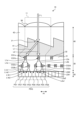
- FIG. 4 is a cross-sectional view schematically showing the structure of a pixel array section according to the embodiment of the present disclosure
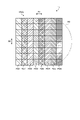
- FIG. 2 is a plan view showing the configuration of a photodiode group according to an embodiment of the present disclosure
- FIG. 3 is a diagram for explaining the principle of a color splitter according to an embodiment of the present disclosure
- FIG. FIG. 4 is a diagram showing an incident state of incident light in a pixel array section according to the embodiment of the present disclosure
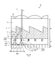
- FIG. 5 is a cross-sectional view schematically showing the structure of a pixel array section according to Modification 1 of the embodiment of the present disclosure
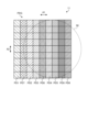
- FIG. 5 is a plan view showing the configuration of a photodiode group according to Modification 1 of the embodiment of the present disclosure
- FIG. 5 is a diagram showing an incident state of incident light in a pixel array section according to Modification 1 of the embodiment of the present disclosure
- FIG. 7 is a diagram showing the configuration of a pixel array section and the incident state of incident light according to Modification 2 of the embodiment of the present disclosure
- FIG. 11 is a plan view showing a configuration of a photodiode group according to Modification 2 of the embodiment of the present disclosure
- FIG. 10 is a diagram showing the configuration of a pixel array section and the incident state of incident light according to Modification 3 of the embodiment of the present disclosure
- FIG. 10 is a cross-sectional view schematically showing the structure of a pixel array section according to Modification 4 of the embodiment of the present disclosure
- FIG. 11 is a cross-sectional view schematically showing the structure of a pixel array section according to Modification 5 of the embodiment of the present disclosure
- FIG. 11 is a diagram showing the configuration of a pixel array section and the incident state of incident light according to Modification 6 of the embodiment of the present disclosure
- FIG. 14 is a perspective view schematically showing the structure of a pixel array section according to Modification 7 of the embodiment of the present disclosure
- FIG. 20 is a plan view showing an example of arrangement of a plurality of photodiode groups according to Modification 8 of the embodiment of the present disclosure
- FIG. 21 is a plan view showing an example of arrangement of a plurality of photodiode groups according to Modification 9 of the embodiment of the present disclosure
- FIG. 21 is a plan view showing an example of the arrangement of a plurality of photodiode groups according to Modification 10 of the embodiment of the present disclosure
- 1 is a block diagram showing a configuration example of an imaging device as an electronic device to which technology according to the present disclosure is applied;
- a photoelectric conversion unit that photoelectrically converts light in one wavelength band is provided on the light incident side, and two photoelectric conversion units that photoelectrically convert light in two other wavelength bands are provided on the side opposite to the light incident side.
- a solid-state imaging device is proposed.
- FIG. 1 is a system configuration diagram showing a schematic configuration example of a solid-state imaging device 1 according to an embodiment of the present disclosure.
- the solid-state imaging device 1 which is a CMOS image sensor, includes a pixel array section 10, a system control section 12, a vertical drive section 13, a column readout circuit section 14, a column signal processing section 15, A horizontal driving unit 16 and a signal processing unit 17 are provided.
- pixel array section 10 system control section 12, vertical drive section 13, column readout circuit section 14, column signal processing section 15, horizontal drive section 16 and signal processing section 17 are on the same semiconductor substrate or are electrically connected. provided on a plurality of stacked semiconductor substrates.
- the pixel array section 10 has photoelectric conversion elements (photodiodes PD1 to PD6 (see FIG. 2), etc.) capable of photoelectrically converting the amount of charge corresponding to the amount of incident light, accumulating it internally, and outputting it as a signal.
- Effective unit pixels 11 are two-dimensionally arranged in a matrix. In addition, in the following description, the effective unit pixel 11 is also called "unit pixel 11".
- the pixel array section 10 includes dummy unit pixels having a structure that does not have photodiodes PD1 to PD6, etc., and light-shielding units in which light from the outside is blocked by shielding the light-receiving surface. Pixels and the like may include regions arranged in rows and/or columns.
- the light-shielding unit pixel may have the same configuration as the effective unit pixel 11 except that the light-receiving surface is light-shielded. Further, hereinafter, the photocharge having the amount of charge corresponding to the amount of incident light may be simply referred to as "charge”, and the unit pixel 11 may be simply referred to as "pixel".
- a pixel driving line LD is formed along the left-right direction in the drawing (pixel arrangement direction of the pixel row) for each row with respect to the matrix-like pixel arrangement, and a vertical pixel wiring is formed for each column.
- the LV is formed along the vertical direction in the drawing (the pixel arrangement direction of the pixel column).
- One end of the pixel drive line LD is connected to an output terminal corresponding to each row of the vertical drive section 13 .
- the column readout circuit section 14 includes at least a circuit that supplies a constant current for each column to the unit pixels 11 in the selected row in the pixel array section 10, a current mirror circuit, a changeover switch for the unit pixels 11 to be read out, and the like.
- the column readout circuit section 14 forms an amplifier together with the transistors in the selected pixels in the pixel array section 10, converts the photoelectric charge signal into a voltage signal, and outputs the voltage signal to the vertical pixel wiring LV.
- the vertical drive section 13 includes a shift register, an address decoder, and the like, and drives each unit pixel 11 of the pixel array section 10 all pixels simultaneously or in units of rows.
- the vertical drive section 13 has a readout scanning system and a sweeping scanning system or a batch sweeping and batch transfer system, although the specific configuration thereof is not shown.
- the readout scanning system sequentially selectively scans the unit pixels 11 of the pixel array section 10 row by row in order to read out pixel signals from the unit pixels 11 .
- sweep scanning is performed ahead of the readout scanning by the time of the shutter speed for the readout rows to be readout scanned by the readout scanning system.
- the electronic shutter operation refers to the operation of discarding unnecessary photocharges accumulated in the photodiodes PD1 to PD6 until immediately before and starting new exposure (starting accumulation of photocharges).
- the signal read out by the readout operation by the readout scanning system corresponds to the amount of incident light after the immediately preceding readout operation or the electronic shutter operation.
- the period from the readout timing of the previous readout operation or the sweep timing of the electronic shutter operation to the readout timing of the current readout operation is the accumulation time (exposure time) of the photocharges in the unit pixel 11.
- the time from batch sweeping to batch transfer is accumulation time (exposure time).
- a pixel signal output from each unit pixel 11 in a pixel row selectively scanned by the vertical driving section 13 is supplied to the column signal processing section 15 through each vertical pixel wiring LV.
- the column signal processing unit 15 performs predetermined signal processing on pixel signals output from each unit pixel 11 of a selected row through the vertical pixel wiring LV for each pixel column of the pixel array unit 10, and performs a predetermined signal processing on the pixel signals after the signal processing. Temporarily holds the pixel signal.
- the column signal processing unit 15 performs at least noise removal processing, such as CDS (Correlated Double Sampling) processing, as signal processing.
- CDS Correlated Double Sampling
- the CDS processing by the column signal processing unit 15 removes pixel-specific fixed pattern noise such as reset noise and variations in the threshold value of the amplification transistor AMP.
- the column signal processing unit 15 may be configured to have, for example, an AD conversion function other than noise removal processing, so that pixel signals are output as digital signals.
- the horizontal driving section 16 includes a shift register, an address decoder, etc., and sequentially selects unit circuits corresponding to the pixel columns of the column signal processing section 15 . Pixel signals processed by the column signal processing unit 15 are sequentially output to the signal processing unit 17 by selective scanning by the horizontal driving unit 16 .
- the system control unit 12 includes a timing generator that generates various timing signals, and controls the vertical driving unit 13, the column signal processing unit 15, the horizontal driving unit 16, etc. based on the various timing signals generated by the timing generator. Drive control.
- the solid-state imaging device 1 further includes a signal processing section 17 and a data storage section (not shown).
- the signal processing unit 17 has at least an addition processing function, and performs various signal processing such as addition processing on the pixel signals output from the column signal processing unit 15 .
- the data storage unit temporarily stores data required for signal processing in the signal processing unit 17 .
- the signal processing unit 17 and the data storage unit may be processed by an external signal processing unit provided on a substrate different from the solid-state imaging device 1, such as a DSP (Digital Signal Processor) or software. 1 may be mounted on the same substrate.
- DSP Digital Signal Processor
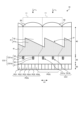
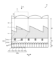
- FIG. 2 is a cross-sectional view schematically showing the structure of the pixel array section 10 according to the embodiment of the present disclosure
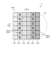
- FIG. 3 is a plan view showing the configuration of the photodiode group PDG according to the embodiment of the present disclosure. .
- the pixel array section 10 includes a semiconductor layer 20, a color splitter layer 30, a prism layer 40, and a plurality of OCLs (on-chip lenses) 50.
- a plurality of OCLs 50, a prism layer 40, a color splitter layer 30, and a semiconductor layer 20 are laminated in order from the side on which incident light L from the outside is incident (hereinafter also referred to as the light incident side). It is
- the semiconductor layer 20 has a semiconductor region (not shown) of a first conductivity type (eg, P-type) and a plurality of semiconductor regions (not shown) of a second conductivity type (eg, N-type).
- a plurality of semiconductor regions of the second conductivity type are formed in the semiconductor region of the first conductivity type so as to be aligned in the plane direction (arrangement direction of the pixels 11) in units of pixels, thereby forming the photodiodes PD1 to PD1 through the PN junction.
- PDs 6 are formed side by side in this order along a given direction A1.
- the photodiodes PD1 to PD6 are examples of photoelectric conversion units. In the following description, the photodiodes PD1 to PD6 are also collectively referred to as "photodiodes PD".
- photodiodes PD1 to PD6 (hereinafter also referred to as "photodiode group PDG") to which the incident light L is incident via the same OCL 50, as shown in FIG.
- Photodiodes PD1 to PD6 are provided respectively. That is, each pixel 11 is provided with a plurality of photodiodes PD1 to PD6.
- a plurality of photodiodes PD1 to PD6 are arranged side by side along a given direction A2.
- the direction A2 is a direction substantially perpendicular to the direction A1.
- the photodiode PD1 is, for example, a photoelectric conversion unit that receives and photoelectrically converts light in a violet wavelength range (hereinafter also referred to as “purple range”).
- the photodiode PD2 is, for example, a photoelectric conversion unit that receives and photoelectrically converts light in a blue wavelength range (hereinafter also referred to as “blue region”).
- the photodiode PD3 is, for example, a photoelectric conversion unit that receives and photoelectrically converts light in a green wavelength range (hereinafter also referred to as “green range”).
- the photodiode PD4 is, for example, a photoelectric conversion unit that receives and photoelectrically converts light in a yellow wavelength region (hereinafter also referred to as “yellow region”).
- the photodiode PD5 is, for example, a photoelectric conversion unit that receives and photoelectrically converts light in an orange wavelength range (hereinafter also referred to as “orange region”).
- the photodiode PD6 is, for example, a photoelectric conversion unit that receives and photoelectrically converts light in a red wavelength range (hereinafter also referred to as “red region”).
- a wiring layer (not shown) is arranged on the surface of the semiconductor layer 20 opposite to the light incident side.
- Such a wiring layer is constructed by forming a plurality of wiring films (not shown) and a plurality of pixel transistors (not shown) in an interlayer insulating film (not shown).
- Such a plurality of pixel transistors read out charges accumulated in the photodiodes PD1 to PD6, respectively.
- a color splitter layer 30 is arranged on the light incident side surface of the semiconductor layer 20 .
- the color splitter layer 30 has a low refractive index layer 31 and a plurality of high refractive index portions 32 .
- the low refractive index layer 31 is composed of a material having a lower refractive index than the high refractive index portion 32.
- Low refractive index layer 31 is made of, for example, metal oxide such as silicon oxide or aluminum oxide, or organic material such as acrylic resin.
- a high refractive index portion 32 having a predetermined shape is provided inside the low refractive index layer 31 .
- the high refractive index portion 32 is made of a material having a higher refractive index than the low refractive index layer 31 .
- the high refractive index portion 32 is composed of, for example, silicon compounds such as silicon nitride and silicon carbide, metal oxides such as titanium oxide, tantalum oxide, niobium oxide, hafnium oxide, indium oxide, and tin oxide, or composite oxides thereof. be done. Also, the high refractive index portion 32 may be composed of an organic substance such as siloxane.
- color splitter CS1 In the color splitter layer 30, a plurality of color splitters CS1 each composed of a high refractive index portion 32 and a low refractive index layer 31 adjacent to the high refractive index portion 32 are arranged.
- Such color splitter CS1 includes color splitter CS1a and color splitter CS1b.
- the color splitter CS1a is arranged, for example, on the light incident side of the photodiode PD2.
- Color splitter CS1b is arranged, for example, on the light incident side of photodiode PD5.
- each pixel 11 is provided with a plurality of color splitters CS1a and CS1b (six in the drawing), and each of the plurality of color splitters CS1a and CS1b is provided with a given pixel. They are arranged side by side along the direction A2. The action of the color splitter CS1 will be described later.
- a prism layer 40 is arranged on the light incident side surface of the color splitter layer 30 .
- the prism layer 40 has a high refractive index layer 41 and a low refractive index layer 42 .
- a low refractive index layer 42 and a high refractive index layer 41 are laminated in order from the light incident side.
- the high refractive index layer 41 is composed of a material having a higher refractive index than the low refractive index layer 42.
- High refractive index layer 41 is composed of, for example, silicon compounds such as silicon nitride and silicon carbide, metal oxides such as titanium oxide, tantalum oxide, niobium oxide, hafnium oxide, indium oxide, and tin oxide, or composite oxides thereof. be done.
- the high refractive index layer 41 may be composed of an organic material such as siloxane.
- a convex portion 41a having a predetermined shape is provided on the surface of the high refractive index layer 41 on the light incident side.
- the low refractive index layer 42 is composed of a material having a lower refractive index than the high refractive index layer 41.
- Low refractive index layer 42 is composed of, for example, a metal oxide such as silicon oxide or aluminum oxide, or an organic material such as acrylic resin.
- a prism portion P composed of a convex portion 41a of a high refractive index layer 41 and a low refractive index layer 42 adjacent to the convex portion 41a is arranged.
- the action of the prism portion P and the like will be described later.
- the OCL 50 is configured, for example, in a hemispherical shape and provided for each pixel 11 .
- the OCL 50 is a lens that collects the incident light L onto the prism portion P of each pixel 11 .
- the OCL 50 is made of, for example, an acrylic resin.
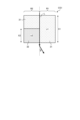
- FIG. 4 is a diagram for explaining the principle of the color splitter CS1 according to the embodiment of the present disclosure.
- the color splitter CS1 has a first region R1 and a second region R2 in which the low refractive index layers 31 and the high refractive index portions 32 are arranged differently in the depth direction.
- the low refractive index layer 31 having a low refractive index (for example, refractive index n1) is arranged along the light incident direction by the length X1.
- a high refractive index portion 32 having a high refractive index (for example, refractive index n2) is arranged along the light incident direction by a length X2.
- the difference in refractive index between the low refractive index layer 31 and the high refractive index portion 32 causes the first A difference occurs in the distance traveled by the incident light L between the region R1 and the second region R2.
- the optical path length D1 of the first region R1 is obtained by the following formula (1).
- D1 n1 ⁇ X1 (1)
- optical path length D2 of the second region R2 is obtained by the following formula (2).
- D2 n1 ⁇ (X1 ⁇ X2)+n2 ⁇ X2 (2)
- the optical path length difference ⁇ D between the first region R1 and the second region R2 is obtained by the following formula (3).
- the incident light L that has passed through the color splitter CS1 travels to the first region R1 with a delay due to the optical path length difference ⁇ D between the first region R1 and the second region R2, as shown in FIG. It bends to the side and is emitted.
- the bending angle ⁇ of the incident light L can be obtained by the following formula (4).
- the bending angle ⁇ of the incident light L depends on the wavelength ⁇ of the incident light L, as shown in the above formula (4). Therefore, by appropriately selecting the refractive indices n1 and n2 of the low refractive index layer 31 and the high refractive index portion 32 according to the respective wavelength ranges, the color splitter CS1 can direct the light of the respective wavelength ranges to desired different directions. can be bent to
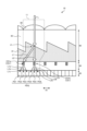
- FIG. 5 is a diagram showing the incident state of the incident light L in the pixel array section 10 according to the embodiment of the present disclosure. As shown in FIG. 5, incident light L having all wavelengths in the visible region is collected by the OCL 50 and reaches the prism portion P by the prism layer 40 .
- the prism unit P divides the incident light L into light L1 in a short wavelength range (for example, a wavelength range from purple to green) and light L2 in a long wavelength range (for example, a wavelength range from yellow to red).
- the prism part P bends the light L1 in the short wavelength range toward the color splitter CS1a of the same pixel 11, and bends the light L2 in the long wavelength range toward the color splitter CS1b of the same pixel 11. .
- the color splitter CS1a splits the light L1 that has reached the color splitter CS1a into light L1a in the purple region, light L1b in the blue region, and light L1c in the green region.
- the color splitter CS1a bends the light L1a in the purple region toward the photodiode PD1, bends the light L1b in the blue region toward the photodiode PD2, and bends the light L1c in the green region toward the photodiode PD3.
- the color splitter CS1b splits the light L2 that has reached the color splitter CS1b into light L2a in the yellow region, light L2b in the orange region, and light L2c in the red region.
- the color splitter CS1b bends the light L2a in the yellow region toward the photodiode PD4, bends the light L2b in the orange region toward the photodiode PD5, and bends the light L2c in the red region toward the photodiode PD6.
- the prism part P and the color splitter CS1 between the OCL 50 and the photodiodes PD1 to PD6, the light beams L1a to L2c having different wavelength ranges are efficiently emitted to the photodiode PD1.
- ⁇ can be incident on PD6.
- the embodiment in one pixel 11, light in six different wavelength ranges (that is, light of six colors) can be efficiently photoelectrically converted. Therefore, according to the embodiment, the image quality of the pixel array section 10 can be improved.
- the prism portion P on the light incident side of the color splitter CS1.
- the prism part P more suitable for splitting light with a wide wavelength range (for example, the incident light L) on the light incident side, the lights L1a to L2c with different wavelength ranges are more efficiently emitted from the photodiode PD1.
- ⁇ PD6 can be made incident.
- the image quality of the pixel array section 10 can be further improved.
- the color splitter CS1 may be arranged between the prism portion P and the photodiodes PD1 to PD6.
- the color splitter CS1 capable of splitting light with a limited wavelength range (for example, the light L1 and L2) with high resolution, the light L1a to L2c with different wavelength ranges can be separated from each other more efficiently by the photodiodes. It can be incident on PD1 to PD6.
- the image quality of the pixel array section 10 can be further improved.
- the color splitter CS1 preferably has a metasurface structure.
- a metasurface structure is a structure in which a plurality of columnar portions formed within one color splitter CS1 are arranged with a period equal to or less than the wavelength ⁇ of the incident light L.
- the effective refractive index of the color splitter CS1 can be changed, so that the lights L1a to L2c having different wavelength ranges can be further bent in desired directions.
- the image quality of the pixel array section 10 can be further improved.
- a plurality of (for example, six) photodiodes PD to which light in the same wavelength band is incident are provided in one pixel 11, and such a plurality of photodiodes PD are provided for a given are arranged side by side along the direction A2.
- the pixel array section 10 can be formed using a pattern that is regularly repeated along the direction A2, so the manufacturing cost of the pixel array section 10 can be reduced.
- a plurality of color filters (not shown) corresponding to respective wavelength ranges may be arranged between the color splitter CS1 and the photodiodes PD1 to PD6.
- FIG. 6 is a cross-sectional view schematically showing the structure of the pixel array section 10 according to Modification 1 of the embodiment of the present disclosure, and corresponds to FIG. 2 of the embodiment.
- FIG. 7 is a plan view showing the configuration of the photodiode group PDG according to Modification 1 of the embodiment of the present disclosure, and corresponds to FIG. 3 of the embodiment.
- the pixel array section 10 according to Modification 1 differs from the embodiment in the configuration of the photodiode group PDG and the configuration of the color splitter layer 30 . Specifically, as shown in FIG. 6, in the semiconductor layer 20, photodiodes PD1, PD7, PD2, PD3, PD8, PD4, PD5, and PD6 are arranged in this order along a given direction A1. be done.
- each pixel 11 is provided with a plurality of photodiodes PD1 to PD8.
- a plurality of photodiodes PD1 to PD8 are arranged side by side along a given direction A2.
- the photodiode PD7 is, for example, a photoelectric conversion unit that receives and photoelectrically converts light in the indigo wavelength range (hereinafter also referred to as “indigo region”).
- the photodiode PD8 is, for example, a photoelectric conversion unit that receives and photoelectrically converts light in a yellow-green wavelength range (hereinafter also referred to as “yellow-green region”).
- the photodiodes PD1 to PD6 are photoelectric conversion units that receive and photoelectrically convert light in the same wavelength range as in the above embodiment, so detailed description thereof will be omitted.
- a color splitter CS2 is arranged in addition to the color splitter CS1.
- Color splitter CS2 is an example of another color splitter.
- the color splitter CS2 is composed of a high refractive index portion 32 and a low refractive index layer 31 adjacent to the high refractive index portion 32, like the color splitter CS1.
- Color splitter CS2 is arranged between color splitter CS1 and photodiode group PDG.
- Color splitter CS2 includes color splitters CS2a-CS2d.
- the color splitter CS2a is arranged, for example, on the light incident side of the boundary between the photodiodes PD1 and PD7.
- Color splitter CS2b is arranged, for example, on the light incident side of the boundary between photodiode PD2 and photodiode PD3.
- the color splitter CS2c is arranged, for example, on the light incident side of the boundary between the photodiodes PD8 and PD4.
- Color splitter CS2d is arranged, for example, on the light incident side of the boundary between photodiode PD5 and photodiode PD6.
- the color splitter CS1a of the color splitter CS1 is arranged, for example, on the light incident side of the boundary between the photodiode PD7 and the photodiode PD2.
- Color splitter CS1b is arranged, for example, on the light incident side of the boundary between photodiode PD4 and photodiode PD5.
- one pixel 11 is provided with a plurality of color splitters CS1a, CS1b, and CS2a to CS2d each (for example, eight).
- a plurality of color splitters CS1a, CS1b, CS2a to CS2d are arranged side by side along a given direction A2.
- FIG. 8 is a diagram showing the incident state of the incident light L in the pixel array section 10 according to Modification 1 of the embodiment of the present disclosure. As shown in FIG. 8 , in Modification 1, incident light L having all wavelength ranges in the visible region is collected by the OCL 50 and reaches the prism portion P by the prism layer 40 .
- the prism unit P according to Modification 1 divides the incident light L into light L1 in a short wavelength range (for example, purple to green wavelength range) and light in a long wavelength range (for example, yellow to red wavelength range). and L2.
- the prism part P according to the modification 1 bends the light L1 in the short wavelength range toward the color splitter CS1a of the same pixel 11, and bends the light L2 in the long wavelength range toward the color splitter CS1b of the same pixel 11.
- the light L1 that has reached the color splitter CS1a is divided into light L1a in the short wavelength range (for example, purple to indigo wavelength range) and light L1a in the long wavelength range (for example, blue to green wavelength range). It splits into light L1b.
- the short wavelength range for example, purple to indigo wavelength range
- light L1a in the long wavelength range for example, blue to green wavelength range
- the color splitter CS1a bends the light L1a in the short wavelength range toward the color splitter CS2a, and bends the light L1b in the long wavelength range toward the color splitter CS2b.
- the light L2 that has reached the color splitter CS1b is divided into light L2a in a short wavelength range (for example, yellow-green to green wavelength range) and light L2a in a long wavelength range (for example, orange to red wavelength range). and the light L2b.
- a short wavelength range for example, yellow-green to green wavelength range
- light L2a in a long wavelength range for example, orange to red wavelength range
- the color splitter CS1b bends the light L2a in the short wavelength range toward the color splitter CS2c, and bends the light L2b in the long wavelength range toward the color splitter CS2d.
- the color splitter CS2a splits the light L1a that has reached the color splitter CS2a into light L1a1 in the violet region and light L1a2 in the indigo region. Furthermore, the color splitter CS2a bends the light L1a1 in the purple region toward the photodiode PD1, and bends the light L1a2 in the blue region toward the photodiode PD7.
- the color splitter CS2b splits the light L1b reaching the color splitter CS2b into light L1b1 in the blue region and light L1b2 in the green region. Furthermore, the color splitter CS2b bends the light L1b1 in the blue region toward the photodiode PD2 and bends the light L1b2 in the green region toward the photodiode PD3.
- the color splitter CS2c splits the light L2a reaching the color splitter CS2c into light L2a1 in the yellow-green region and light L2a2 in the green region. Furthermore, the color splitter CS2c bends the light L2a1 in the yellow-green region toward the photodiode PD8, and bends the light L2a2 in the green region toward the photodiode PD4.
- the color splitter CS2d splits the light L2b reaching the color splitter CS2d into light L2b1 in the orange region and light L2b2 in the red region. Furthermore, the color splitter CS2d bends the light L2b1 in the orange region toward the photodiode PD5 and bends the light L2b2 in the red region toward the photodiode PD6.
- Modification 1 in one pixel 11, light in eight different wavelength ranges (that is, light of eight colors) can be efficiently photoelectrically converted. Therefore, according to Modification 1, the image quality of the pixel array section 10 can be improved.
- the color splitter CS2 preferably has a metasurface structure. As a result, since the effective refractive index of the color splitter CS2 can be changed, the lights L1a1 to L2b2 having different wavelength ranges can be further bent in desired directions.
- the image quality of the pixel array section 10 can be further improved.
- a plurality of color filters (not shown) corresponding to respective wavelength ranges may be arranged between the color splitter CS2 and the photodiodes PD1 to PD8.
- FIG. 9 is a diagram showing the configuration of the pixel array section 10 and the incident state of the incident light L according to Modification 2 of the embodiment of the present disclosure, and is a diagram corresponding to FIG. 5 of the embodiment.
- FIG. 10 is a plan view showing the configuration of the photodiode group PDG according to Modification 2 of the embodiment of the present disclosure, and corresponds to FIG. 3 of the embodiment.
- the configuration of the color splitter layer 30 and the function of the prism section P are different from those of the embodiment. Specifically, as shown in FIG. 9, in the semiconductor layer 20, photodiodes PD1, PD7, PD2, PD3, PD8, PD4, PD5, PD9, and PD6 are arranged in this order along a given direction A1. formed by
- the photodiodes PD1 to PD9 to which the incident light L is incident via the same OCL 50 are each provided with a plurality of (nine in the figure) photodiodes PD1 to PD9. That is, each pixel 11 is provided with a plurality of photodiodes PD1 to PD9. A plurality of photodiodes PD1 to PD9 are arranged side by side along a given direction A2.
- the photodiode PD9 is, for example, a photoelectric conversion unit that receives and photoelectrically converts light in a reddish-orange wavelength range (hereinafter also referred to as a "reddish-orange range").
- the photodiodes PD1 to PD8 are photoelectric conversion units that receive and photoelectrically convert light in the same wavelength range as in the above-described embodiment and modification 1, so detailed description thereof will be omitted.
- color splitter layer 30 is provided with a color splitter CS1 having a configuration different from that of the embodiment.
- color splitter CS1 includes color splitters CS1a, CS1b, and CS1c.
- the color splitter CS1a is arranged, for example, on the light incident side of the photodiode PD7.
- Color splitter CS1b is arranged, for example, on the light incident side of photodiode PD8.
- Color splitter CS1c is arranged, for example, on the light incident side of photodiode PD9.
- each pixel 11 is provided with a plurality (for example, nine) of color splitters CS1a to CS1c.
- a plurality of color splitters CS1a to CS1c are arranged side by side along a given direction A2.
- incident light L having all wavelength ranges in the visible region is collected by the OCL 50 and reaches the prism portion P by the prism layer 40 .
- the prism unit P according to Modification 2 divides the incident light L into light L1 in the short wavelength range (for example, purple to blue wavelength range) and light in the middle wavelength range (for example, green to yellow wavelength range). It is split into light L2 and light L3 in a long wavelength range (for example, wavelength range from orange to red).
- the prism part P according to the modification 2 bends the light L1 in the short wavelength range toward the color splitter CS1a of the same pixel 11, and bends the light L2 in the middle wavelength range toward the color splitter CS1b of the same pixel 11.
- the prism portion P according to Modification 2 bends the light L3 in the long wavelength region toward the color splitter CS1c of the same pixel 11 .
- the color splitter CS1a splits the light L1 that has reached the color splitter CS1a into light L1a in the purple region, light L1b in the blue region, and light L1c in the blue region.
- the color splitter CS1a bends the light L1a in the purple region toward the photodiode PD1, bends the light L1b in the blue region toward the photodiode PD7, and bends the light L1c in the blue region toward the photodiode PD2. flex.
- the color splitter CS1b splits the light L2 that has reached the color splitter CS1b into light L2a in the green region, light L2b in the yellow-green region, and light L2c in the yellow region.
- the color splitter CS1b bends the light L2a in the green region toward the photodiode PD3, bends the light L2b in the yellow-green region toward the photodiode PD8, and bends the light L2c in the yellow region toward the photodiode PD4. flex.
- the color splitter CS1c splits the light L3 reaching the color splitter CS1c into light L3a in the orange region, light L3b in the red-orange region, and light L3c in the red region.
- the color splitter CS1c bends the light L3a in the orange region toward the photodiode PD5, bends the light L3b in the reddish-orange region toward the photodiode PD9, and bends the light L3c in the red region toward the photodiode PD6. flex.
- the incident light L is split into three different wavelength bands in the prism part P, and the three different wavelength bands are made incident on the three color splitters CS1a to CS1c.
- the lights L1a to L3c having different wavelength ranges can be efficiently made incident on the photodiodes PD1 to PD9.
- a plurality of color filters (not shown) corresponding to respective wavelength ranges may be arranged between the color splitter CS1 and the photodiodes PD1 to PD9.
- FIG. 11 is a diagram showing the configuration of the pixel array section 10 and the incident state of the incident light L according to Modification 3 of the embodiment of the present disclosure, and is a diagram corresponding to FIG. 5 of the embodiment.
- the pixel array section 10 according to Modification 3 differs from the embodiment in the configuration of the photodiode group PDG and the function of the color splitter layer 30 . Specifically, as shown in FIG. 11, in the semiconductor layer 20, photodiodes PD2 to PD6 are arranged in this order along a given direction A1.
- the photodiodes PD2 to PD6 to which the incident light L is incident via the same OCL 50 are each provided with a plurality (for example, five) of the photodiodes PD2 to PD6. That is, each pixel 11 is provided with a plurality of photodiodes PD2 to PD6.
- a plurality of photodiodes PD2 to PD6 are arranged side by side along a given direction A2 (see FIG. 3). Note that the photodiodes PD2 to PD6 are photoelectric conversion units that receive and photoelectrically convert light in the same wavelength range as in the above-described embodiment, so detailed description thereof will be omitted.
- the color splitter CS1 of Modification 3 includes color splitters CS1a and CS1b.
- Color splitter CS1a is arranged, for example, on the light incident side of photodiode PD3.
- Color splitter CS1b is arranged, for example, on the light incident side of photodiode PD5.
- each pixel 11 is provided with a plurality of color splitters CS1a and CS1b (for example, five) each.
- a plurality of color splitters CS1a and CS1b are arranged side by side along a given direction A2.
- incident light L having all wavelength ranges in the visible region is collected by the OCL 50 and reaches the prism portion P by the prism layer 40 .
- the prism unit P according to Modification 3 divides the incident light L into light L1 in a short wavelength range (for example, blue to yellow wavelength range) and light in a long wavelength range (for example, yellow to red wavelength range). and L2.
- the prism part P according to the third modification bends the light L1 in the short wavelength range toward the color splitter CS1a of the same pixel 11, and bends the light L2 in the long wavelength range toward the color splitter CS1b of the same pixel 11.
- the color splitter CS1a splits the light L1 that has reached the color splitter CS1a into light L1a in the blue region, light L1b in the green region, and light L1c in the yellow region.
- the color splitter CS1a bends the light L1a in the blue region toward the photodiode PD2, bends the light L1b in the green region toward the photodiode PD3, and bends the light L1c in the yellow region toward the photodiode PD4.
- the color splitter CS1b splits the light L2 that has reached the color splitter CS1b into light L2a in the yellow region, light L2b in the orange region, and light L2c in the red region.
- the color splitter CS1b bends the light L2a in the yellow region toward the photodiode PD4, bends the light L2b in the orange region toward the photodiode PD5, and bends the light L2c in the red region toward the photodiode PD6.
- each pixel 11 can efficiently photoelectrically convert light in five different wavelength ranges (that is, light of five colors). Image quality can be improved.
- a pair of mutually adjacent color splitters CS1a and CS1b cause light in the same wavelength range (here, light in the yellow region) to enter the same photodiode PD4.
- FIG. 11 shows an example in which light in the same wavelength range is incident on the same photodiode PD from a pair of mutually adjacent color splitters CS1a and CS1b based on the configuration of the above-described embodiment (FIG. 2, etc.).
- the present disclosure is not limited to such examples.
- light in the same wavelength band may be incident on the same photodiode PD from a pair of mutually adjacent color splitters CS2 or the like based on the configuration of Modification 1 (FIG. 6, etc.).
- light in the same wavelength band may be incident on the same photodiode PD from a pair of mutually adjacent color splitters CS1 based on the configuration of Modification 2 (FIG. 9, etc.).
- FIG. 12 is a cross-sectional view schematically showing the structure of the pixel array section 10 according to Modification 4 of the embodiment of the present disclosure. As shown in FIG. 12, in Modification 4, a plurality of hemispherical microlenses 51 are provided between the prism portion P and the color splitter CS1.
- Such a plurality of microlenses 51 are arranged, for example, on the light incident sides of the color splitters CS1a and CS1b.
- the plurality of microlenses 51 converge the lights L1 and L2 (see FIG. 5) incident on the color splitters CS1a and CS1b toward the color splitters CS1a and CS1b.
- the amount of light L1 and L2 incident on the color splitters CS1a and CS1b can be increased, so that the sensitivities of the photodiodes PD1 to PD6 can be improved.
- the microlenses 51 are not limited to hemispherical lenses, and may be metalens having a metasurface structure. This also makes it possible to improve the sensitivity of the photodiodes PD1 to PD6.
- FIG. 13 is a cross-sectional view schematically showing the structure of the pixel array section 10 according to Modification 5 of the embodiment of the present disclosure. As shown in FIG. 13, in modification 5, a plurality of microlenses 52 are provided between the color splitter CS1 and the photodiode group PDG.
- Such a plurality of microlenses 52 are arranged, for example, on the light incident sides of the photodiodes PD1 to PD6. Then, the plurality of microlenses 52 converge the lights L1a to L2c (see FIG. 5) incident on the photodiodes PD1 to PD6 toward the photodiodes PD1 to PD6.
- the amount of light L1a-L2c incident on the photodiodes PD1-PD6 can be increased, and the sensitivity of the photodiodes PD1-PD6 can be improved.
- the microlenses 52 are not limited to hemispherical lenses, and may be metalens having a metasurface structure. This also makes it possible to improve the sensitivity of the photodiodes PD1 to PD6.
- FIG. 14 is a cross-sectional view schematically showing the structure of the pixel array section 10 according to Modification 6 of the embodiment of the present disclosure.
- the relative positional relationship among the OCL 50, the prism portion P and the color splitter CS1 in each pixel 11 may be adjusted according to the distance (image height) from the center of the pixel array portion 10, for example. Good (so-called pupil correction).
- the light beams L1a to L2c can be incident on the photodiodes PD1 to PD6 substantially uniformly. Therefore, according to Modification 6, the image quality of the pixel array section 10 can be further improved.
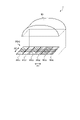
- FIG. 15 is a perspective view schematically showing the structure of the pixel array section 10 according to Modification 7 of the embodiment of the present disclosure. Note that FIG. 15 omits illustration of components other than the OCL 50 and the photodiode group PDG for easy understanding.
- the OCL 50 is not a hemispherical lens but a semi-cylindrical lens structure (so-called cylinder lens structure).
- the axial direction of the OCL 50 having the cylindrical lens structure faces the same direction as the direction A2 in which the plurality of photodiodes PD (for example, photodiodes PD1) on which light in the same wavelength band is incident is arranged.
- the light can be made substantially evenly incident on the plurality of photodiodes PD on which the light of the same wavelength band is incident. Therefore, according to Modification 7, the image quality of the pixel array section 10 can be further improved.
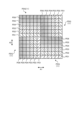
- ⁇ Modifications 8 and 9> 16 and 17 are plan views showing examples of the arrangement of a plurality of photodiode groups PDG according to modified examples 8 and 9 of the embodiment of the present disclosure. As shown in FIG. 16, in Modification Example 8, the directions in which the plurality of photodiodes PD on which light in the same wavelength band is incident are different from each other in the adjacent photodiode groups PDG.
- a plurality of photodiodes PD on which light in the same wavelength band is incident are arranged along the direction A2.
- a plurality of photodiodes PD into which light in the same wavelength band is incident are arranged along the direction A1.
- the image quality of the pixel array section 10 can be further improved.
- the arrangement example of the photodiode groups PDG adjacent to each other is not limited to the example in FIG. 16, and the arrangement may be changed as shown in FIG. 17, for example. This also makes it possible to further improve the image quality of the pixel array section 10 .
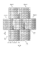
- FIG. 18 is a plan view showing an example of the arrangement of a plurality of photodiode groups PDG according to Modification 10 of the embodiment of the present disclosure.
- a plurality of photodiode groups PDG that is, a plurality of pixels 11
- the prism section P (see FIG. 2) and the color splitter CS1 (see FIG. 2) are arranged between the photodiode group PDG and the OCL 50 (see FIG. 2), thereby improving the image quality of the pixel array section 10. can be improved.
- the solid-state imaging device 1 includes multiple photoelectric conversion units (photodiodes PD), an on-chip lens (OCL 50), a prism unit P, and multiple color splitters CS1.
- a plurality of photoelectric conversion units (photodiodes PD) are arranged in a matrix in the semiconductor layer 20 .
- the on-chip lens (OCL 50) is arranged closer to the light incident side than the semiconductor layer 20 so as to be shared by a plurality of photoelectric conversion units (photodiodes PD).
- the prism part P is arranged between the on-chip lens (OCL 50) and the plurality of photoelectric conversion parts (photodiodes PD).
- the plurality of color splitters CS1 are arranged between the prism portion P and the plurality of photoelectric conversion portions (photodiodes PD).
- the image quality of the pixel array section 10 can be improved.
- the color splitter CS1 has a metasurface structure.
- the solid-state imaging device 1 further includes another color splitter (color splitter CS2) arranged between the color splitter CS1 and the plurality of photoelectric conversion units (photodiodes PD).
- color splitter CS2 another color splitter arranged between the color splitter CS1 and the plurality of photoelectric conversion units (photodiodes PD).
- the image quality of the pixel array section 10 can be improved.
- light in the same wavelength range is incident on some of the photoelectric conversion units (photodiodes PD).
- a plurality of photoelectric conversion units (photodiodes PD) to which light in the same wavelength band is incident are arranged side by side along a given direction A2.
- the on-chip lens (OCL 50) has a cylindrical lens structure having an axial direction that is the same as the given direction A2.
- the solid-state imaging device 1 further includes a plurality of microlenses 51 and 52 arranged between the prism portion P and the plurality of photoelectric conversion portions (photodiodes PD).
- a pair of color splitters CS1a and CS1b adjacent to each other cause light in the same wavelength range to enter the same photoelectric conversion section (photodiode PD).
- the solid-state imaging device 1 includes a plurality of photoelectric conversion units (photodiodes PD) and an on-chip lens (OCL 50).
- a plurality of photoelectric conversion units (photodiodes PD) are arranged in a matrix in the semiconductor layer 20 .
- the on-chip lens (OCL 50) is arranged closer to the light incident side than the semiconductor layer 20 so as to be shared by a plurality of photoelectric conversion units (photodiodes PD).
- a plurality of photoelectric conversion units (photodiodes PD) sharing one on-chip lens (OCL 50) respectively receive light in five or more different wavelength ranges.
- the image quality of the pixel array section 10 can be improved.
- the present disclosure is not limited to application to solid-state imaging devices. That is, the present disclosure applies to general electronic devices having a solid-state imaging device, such as a camera module, an imaging device, a mobile terminal device having an imaging function, or a copier using a solid-state imaging device as an image reading unit, in addition to the solid-state imaging device. applicable.
- a solid-state imaging device such as a camera module, an imaging device, a mobile terminal device having an imaging function, or a copier using a solid-state imaging device as an image reading unit, in addition to the solid-state imaging device.
- imaging devices examples include digital still cameras and video cameras.
- Mobile terminal devices having such an imaging function include, for example, smartphones and tablet terminals.
- FIG. 19 is a block diagram showing a configuration example of an imaging device as the electronic device 100 to which the technology according to the present disclosure is applied.
- the electronic device 100 in FIG. 19 is, for example, an imaging device such as a digital still camera or a video camera, or an electronic device such as a mobile terminal device such as a smart phone or a tablet terminal.
- electronic device 100 includes lens group 101, solid-state image sensor 102, DSP circuit 103, frame memory 104, display unit 105, recording unit 106, operation unit 107, and power supply unit 108. Configured.
- the DSP circuit 103 the frame memory 104 , the display section 105 , the recording section 106 , the operation section 107 and the power supply section 108 are interconnected via a bus line 109 .
- the lens group 101 captures incident light (image light) from a subject and forms an image on the imaging surface of the solid-state imaging device 102 .
- the solid-state imaging device 102 corresponds to the solid-state imaging device 1 according to the above-described embodiment, and converts the amount of incident light imaged on the imaging surface by the lens group 101 into an electric signal for each pixel and outputs the electric signal as a pixel signal. do.
- the DSP circuit 103 is a camera signal processing circuit that processes signals supplied from the solid-state imaging device 102 .
- a frame memory 104 temporarily holds the image data processed by the DSP circuit 103 in frame units.
- the display unit 105 is composed of, for example, a panel-type display device such as a liquid crystal panel or an organic EL (Electro Luminescence) panel, and displays moving images or still images captured by the solid-state imaging device 102 .
- a recording unit 106 records image data of a moving image or a still image captured by the solid-state imaging device 102 in a recording medium such as a semiconductor memory or a hard disk.
- the operation unit 107 issues operation commands for various functions of the electronic device 100 according to the user's operation.
- the power supply unit 108 appropriately supplies various power supplies to the DSP circuit 103, the frame memory 104, the display unit 105, the recording unit 106, and the operating unit 107, to these supply targets.
- the image quality of the pixel array section 10 can be improved.
- the present technology can also take the following configuration.
- the solid-state imaging device according to any one of (1) to (6), wherein the pair of color splitters adjacent to each other causes light in the same wavelength range to enter the same photoelectric conversion section.
- the plurality of photoelectric conversion units sharing one on-chip lens respectively receive light of five or more different wavelength ranges.
- the solid-state imaging device is a plurality of photoelectric conversion units arranged in a matrix in a semiconductor layer; an on-chip lens arranged closer to the light incident side than the semiconductor layer so as to be shared by the plurality of photoelectric conversion units; a prism unit disposed between the on-chip lens and the plurality of photoelectric conversion units;
- An electronic device comprising: a plurality of color splitters arranged between the prism section and the plurality of photoelectric conversion sections. (11) The electronic device according to (10), wherein the color splitter has a metasurface structure.
- the solid-state imaging device is The electronic device according to (10) or (11), further comprising another color splitter arranged between the color splitter and the plurality of photoelectric conversion units.
- Light in the same wavelength range is incident on some of the photoelectric conversion units, The electronic device according to any one of (10) to (12), wherein the plurality of photoelectric conversion units to which light in the same wavelength band is incident are arranged side by side along a given direction.
- the electronic device according to (13), wherein the on-chip lens has a cylinder lens structure having an axial direction that is the same as the given direction.
- the solid-state imaging device is The electronic device according to any one of (10) to (14), further comprising a plurality of microlenses arranged between the prism section and the plurality of photoelectric conversion sections.
- the plurality of photoelectric conversion units sharing one on-chip lens respectively receive light in five or more different wavelength ranges.
- the solid-state imaging device is a plurality of photoelectric conversion units arranged in a matrix in a semiconductor layer; an on-chip lens arranged on the light incident side of the semiconductor layer so as to be shared by the plurality of photoelectric conversion units; has An electronic device, wherein the plurality of photoelectric conversion units sharing one on-chip lens respectively receive light in five or more different wavelength ranges.
Landscapes
- Physics & Mathematics (AREA)
- General Physics & Mathematics (AREA)
- Optics & Photonics (AREA)
- Color Television Image Signal Generators (AREA)
- Solid State Image Pick-Up Elements (AREA)
Abstract
本開示に係る固体撮像素子(1)は、複数の光電変換部と、オンチップレンズと、プリズム部(P)と、複数のカラースプリッタCS1と、を備える。複数の光電変換部は、半導体層(20)内にマトリックス状に並んで配置される。オンチップレンズは、複数の光電変換部が共有するように半導体層(20)よりも光入射側に配置される。プリズム部(P)は、オンチップレンズと複数の光電変換部との間に配置される。複数のカラースプリッタ(CS1)は、プリズム部(P)と複数の光電変換部との間に配置される。
Description
本開示は、固体撮像素子および電子機器に関する。
近年、デジタルカメラは、ますます普及が進んでおり、その中心部品である固体撮像素子(イメージセンサ)の需要はますます高まっている。これに伴い、固体撮像素子では高画質化や高機能化を実現するための技術開発が盛んに行われている(たとえば、特許文献1参照)。
しかしながら、上記の従来技術では、画質を向上させるという点で更なる改善の余地があった。
そこで、本開示では、画質を向上させることができる固体撮像素子および電子機器を提案する。
本開示によれば、固体撮像素子が提供される。固体撮像素子は、複数の光電変換部と、オンチップレンズと、プリズム部と、複数のカラースプリッタと、を備える。複数の光電変換部は、半導体層内にマトリックス状に並んで配置される。オンチップレンズは、複数の前記光電変換部が共有するように前記半導体層よりも光入射側に配置される。プリズム部は、前記オンチップレンズと複数の前記光電変換部との間に配置される。複数のカラースプリッタは、前記プリズム部と複数の前記光電変換部との間に配置される。
本開示によれば、画質を向上させることができる固体撮像素子および電子機器を提供することができる。なお、ここに記載された効果は必ずしも限定されるものではなく、本開示中に記載されたいずれかの効果であってもよい。
以下に、本開示の各実施形態について図面に基づいて詳細に説明する。なお、以下の各実施形態において、同一の部位には同一の符号を付することにより重複する説明を省略する。
近年、デジタルカメラは、ますます普及が進んでおり、その中心部品である固体撮像素子(イメージセンサ)の需要はますます高まっている。これに伴い、固体撮像素子では高画質化や高機能化を実現するための技術開発が盛んに行われている。
たとえば、光入射側に1つの波長域の光を光電変換する光電変換部が設けられ、光入射側とは反対側に別の2つの波長域の光をそれぞれ光電変換する2つの光電変換部が設けられる固体撮像素子が提案されている。
しかしながら、上記の従来技術では、3つの異なる波長域の光しか光電変換できないため、画質を向上させるという点で更なる改善の余地があった。
そこで、上述の問題点を克服し、固体撮像素子の画質を向上させることができる技術の実現が期待されている。
[固体撮像素子の構成]
図1は、本開示の実施形態に係る固体撮像素子1の概略構成例を示すシステム構成図である。図1に示すように、CMOSイメージセンサである固体撮像素子1は、画素アレイ部10と、システム制御部12と、垂直駆動部13と、カラム読出し回路部14と、カラム信号処理部15と、水平駆動部16と、信号処理部17とを備える。
図1は、本開示の実施形態に係る固体撮像素子1の概略構成例を示すシステム構成図である。図1に示すように、CMOSイメージセンサである固体撮像素子1は、画素アレイ部10と、システム制御部12と、垂直駆動部13と、カラム読出し回路部14と、カラム信号処理部15と、水平駆動部16と、信号処理部17とを備える。
これら画素アレイ部10、システム制御部12、垂直駆動部13、カラム読出し回路部14、カラム信号処理部15、水平駆動部16および信号処理部17は、同一の半導体基板上または電気的に接続された複数の積層半導体基板上に設けられる。
画素アレイ部10には、入射光量に応じた電荷量を光電変換して内部に蓄積し、信号として出力することが可能な光電変換素子(フォトダイオードPD1~PD6(図2参照)など)を有する有効単位画素11が行列状に2次元配置されている。なお、以下の説明では、有効単位画素11を「単位画素11」とも呼称する。
また、画素アレイ部10は、有効単位画素11の他に、フォトダイオードPD1~PD6等を持たない構造のダミー単位画素や、受光面を遮光することで外部からの光入射が遮断された遮光単位画素等が、行及び/又は列状に配置されている領域を含む場合がある。
なお、遮光単位画素は、受光面が遮光された構造である以外は、有効単位画素11と同様の構成を備えていてもよい。また、以下では、入射光量に応じた電荷量の光電荷を、単に「電荷」とも呼称し、単位画素11を、単に「画素」とも呼称する場合もある。
画素アレイ部10には、行列状の画素配列に対して、行ごとに画素駆動線LDが図面中の左右方向(画素行の画素の配列方向)に沿って形成され、列ごとに垂直画素配線LVが図面中の上下方向(画素列の画素の配列方向)に沿って形成される。画素駆動線LDの一端は、垂直駆動部13の各行に対応した出力端に接続される。
カラム読出し回路部14は、少なくとも、画素アレイ部10内の選択行における単位画素11に列ごとに定電流を供給する回路、カレントミラー回路および読出し対象となる単位画素11の切替えスイッチなどを含む。
そして、カラム読出し回路部14は、画素アレイ部10内の選択画素におけるトランジスタとともに増幅器を構成し、光電荷信号を電圧信号に変換して垂直画素配線LVに出力する。
垂直駆動部13は、シフトレジスタやアドレスデコーダなどを含み、画素アレイ部10の各単位画素11を、全画素同時や行単位などで駆動する。この垂直駆動部13は、その具体的な構成については図示を省略するが、読出し走査系と、掃出し走査系あるいは一括掃出しおよび一括転送系とを有する構成となっている。
読出し走査系は、単位画素11から画素信号を読み出すために、画素アレイ部10の単位画素11を行単位で順に選択走査する。行駆動(ローリングシャッタ動作)の場合、掃出しについては、読出し走査系によって読出し走査が行われる読出し行に対して、その読出し走査よりもシャッタスピードの時間分だけ先行して掃出し走査が行なわれる。
また、グローバル露光(グローバルシャッタ動作)の場合は、一括転送よりもシャッタスピードの時間分先行して一括掃出しが行なわれる。このような掃出しにより、読出し行の単位画素11のフォトダイオードPD1~PD6などから不要な電荷が掃出し(リセット)される。そして、不要電荷の掃出し(リセット)により、いわゆる電子シャッタ動作が行われる。
ここで、電子シャッタ動作とは、直前までフォトダイオードPD1~PD6などに溜まっていた不要な光電荷を捨てて、新たに露光を開始する(光電荷の蓄積を開始する)動作のことをいう。
読出し走査系による読出し動作によって読み出される信号は、その直前の読出し動作または電子シャッタ動作以降に入射した光量に対応するものである。行駆動の場合は、直前の読出し動作による読出しタイミングまたは電子シャッタ動作による掃出しタイミングから、今回の読出し動作による読出しタイミングまでの期間が、単位画素11における光電荷の蓄積時間(露光時間)となる。グローバル露光の場合は、一括掃出しから一括転送までの時間が蓄積時間(露光時間)となる。
垂直駆動部13によって選択走査された画素行の各単位画素11から出力される画素信号は、垂直画素配線LVの各々を通してカラム信号処理部15に供給される。カラム信号処理部15は、画素アレイ部10の画素列ごとに、選択行の各単位画素11から垂直画素配線LVを通して出力される画素信号に対して所定の信号処理を行うとともに、信号処理後の画素信号を一時的に保持する。
具体的には、カラム信号処理部15は、信号処理として少なくとも、ノイズ除去処理、たとえばCDS(Correlated Double Sampling:相関二重サンプリング)処理を行う。このカラム信号処理部15によるCDS処理により、リセットノイズや増幅トランジスタAMPの閾値ばらつきなどの画素固有の固定パターンノイズが除去される。
なお、カラム信号処理部15には、ノイズ除去処理以外に、たとえば、AD変換機能を持たせて、画素信号をデジタル信号として出力するように構成することもできる。
水平駆動部16は、シフトレジスタやアドレスデコーダなどを含み、カラム信号処理部15の画素列に対応する単位回路を順番に選択する。この水平駆動部16による選択走査により、カラム信号処理部15で信号処理された画素信号が順番に信号処理部17に出力される。
システム制御部12は、各種のタイミング信号を生成するタイミングジェネレータなどを含み、タイミングジェネレータで生成された各種のタイミング信号を基に、垂直駆動部13、カラム信号処理部15、水平駆動部16などの駆動制御を行う。
固体撮像素子1は、さらに、信号処理部17と、図示しないデータ格納部とを備える。信号処理部17は、少なくとも加算処理機能を有し、カラム信号処理部15から出力される画素信号に対して加算処理などの種々の信号処理を行う。
データ格納部は、信号処理部17での信号処理にあたって、その処理に必要なデータを一時的に格納する。これら信号処理部17およびデータ格納部については、固体撮像素子1とは別の基板に設けられる外部信号処理部、たとえばDSP(Digital Signal Processor)やソフトウェアによる処理であってもよいし、固体撮像素子1と同じ基板上に搭載されてもよい。
[画素アレイ部の構成]
つづいて、画素アレイ部10の詳細な構成について、図2~図5を参照しながら説明する。図2は、本開示の実施形態に係る画素アレイ部10の構造を模式的に示す断面図であり、図3は、本開示の実施形態に係るフォトダイオード群PDGの構成を示す平面図である。
つづいて、画素アレイ部10の詳細な構成について、図2~図5を参照しながら説明する。図2は、本開示の実施形態に係る画素アレイ部10の構造を模式的に示す断面図であり、図3は、本開示の実施形態に係るフォトダイオード群PDGの構成を示す平面図である。
図2に示すように、画素アレイ部10は、半導体層20と、カラースプリッタ層30と、プリズム層40と、複数のOCL(オンチップレンズ)50とを備える。そして、画素アレイ部10では、外部からの入射光Lが入射する側(以下、光入射側とも呼称する。)から順に、複数のOCL50、プリズム層40、カラースプリッタ層30および半導体層20が積層されている。
半導体層20は、第1導電型(たとえば、P型)の半導体領域(図示せず)と、第2導電型(たとえば、N型)の複数の半導体領域(図示せず)とを有する。そして、第1導電型の半導体領域内に、第2導電型の複数の半導体領域が画素単位で平面方向(画素11の配列方向)に並んで形成されることにより、PN接合によるフォトダイオードPD1~PD6が、所与の方向A1に沿ってこの順に並んで形成される。
フォトダイオードPD1~PD6は、光電変換部の一例である。なお、以下の説明では、フォトダイオードPD1~PD6を総称して、「フォトダイオードPD」とも呼称する。
また、同じOCL50を介して入射光Lが入射するフォトダイオードPD1~PD6(以下、「フォトダイオード群PDG」とも呼称する。)では、図3に示すように、それぞれ複数個(図では6個)ずつのフォトダイオードPD1~PD6が設けられる。すなわち、1つの画素11には、フォトダイオードPD1~PD6が複数個ずつ設けられる。
そして、複数個ずつのフォトダイオードPD1~PD6は、すべて所与の方向A2に沿って並んで配置される。かかる方向A2は、方向A1と略垂直な方向である。
フォトダイオードPD1は、たとえば、紫色の波長域(以下、「紫色領域」とも呼称する。)の光を受光して光電変換する光電変換部である。フォトダイオードPD2は、たとえば、青色の波長域(以下、「青色領域」とも呼称する。)の光を受光して光電変換する光電変換部である。
フォトダイオードPD3は、たとえば、緑色の波長域(以下、「緑色領域」とも呼称する。)の光を受光して光電変換する光電変換部である。フォトダイオードPD4は、たとえば、黄色の波長域(以下、「黄色領域」とも呼称する。)の光を受光して光電変換する光電変換部である。
フォトダイオードPD5は、たとえば、橙色の波長域(以下、「橙色領域」とも呼称する。)の光を受光して光電変換する光電変換部である。フォトダイオードPD6は、たとえば、赤色の波長域(以下、「赤色領域」とも呼称する。)の光を受光して光電変換する光電変換部である。
なお、半導体層20における光入射側とは反対側の面には、図示しない配線層が配置される。かかる配線層は、層間絶縁膜(図示せず)内に複数の配線膜(図示せず)および複数の画素トランジスタ(図示せず)が形成されることにより構成される。かかる複数の画素トランジスタは、フォトダイオードPD1~PD6にそれぞれ蓄積された電荷の読み出しなどを行う。
半導体層20における光入射側の面には、カラースプリッタ層30が配置される。カラースプリッタ層30は、低屈折率層31および複数の高屈折率部32を有する。
低屈折率層31は、高屈折率部32よりも低い屈折率を有する材料で構成される。低屈折率層31は、たとえば、酸化シリコンや酸化アルミニウムなどの金属酸化物、またはアクリル樹脂などの有機物で構成される。
低屈折率層31の内部には、所定の形状を有する高屈折率部32が設けられる。高屈折率部32は、低屈折率層31よりも高い屈折率を有する材料で構成される。高屈折率部32は、たとえば、窒化シリコン、炭化シリコンなどのシリコン化合物、酸化チタン、酸化タンタル、酸化ニオブ、酸化ハフニウム、酸化インジウム、酸化スズなどの金属酸化物、あるいはこれらの複合酸化物で構成される。また、高屈折率部32は、シロキサンなどの有機物から構成されてもよい。
カラースプリッタ層30には、高屈折率部32と、かかる高屈折率部32に隣接する低屈折率層31とで構成される複数のカラースプリッタCS1が配置される。かかるカラースプリッタCS1は、カラースプリッタCS1aおよびカラースプリッタCS1bを含む。
カラースプリッタCS1aは、たとえば、フォトダイオードPD2の光入射側に配置される。カラースプリッタCS1bは、たとえば、フォトダイオードPD5の光入射側に配置される。
また、図3に示すように、1つの画素11には、カラースプリッタCS1a、CS1bがそれぞれ複数個(図では6個)ずつ設けられ、複数個ずつのカラースプリッタCS1a、CS1bは、すべて所与の方向A2に沿って並んで配置される。カラースプリッタCS1の作用などについては後述する。
カラースプリッタ層30における光入射側の面には、プリズム層40が配置される。プリズム層40は、高屈折率層41と、低屈折率層42とを有する。そして、プリズム層40では、光入射側から順に、低屈折率層42および高屈折率層41が積層されている。
高屈折率層41は、低屈折率層42よりも高い屈折率を有する材料で構成される。高屈折率層41は、たとえば、窒化シリコン、炭化シリコンなどのシリコン化合物、酸化チタン、酸化タンタル、酸化ニオブ、酸化ハフニウム、酸化インジウム、酸化スズなどの金属酸化物、あるいはこれらの複合酸化物で構成される。また、高屈折率層41は、シロキサンなどの有機物から構成されてもよい。
また、高屈折率層41における光入射側の面には、所定の形状を有する凸部41aが設けられる。
低屈折率層42は、高屈折率層41よりも低い屈折率を有する材料で構成される。低屈折率層42は、たとえば、酸化シリコンや酸化アルミニウムなどの金属酸化物、またはアクリル樹脂などの有機物で構成される。
プリズム層40には、高屈折率層41の凸部41aと、かかる凸部41aに隣接する低屈折率層42とで構成されるプリズム部Pが配置される。かかるプリズム部Pの作用などについては後述する。
OCL50は、たとえば、半球形状に構成され、画素11ごとに設けられる。OCL50は、各画素11のプリズム部Pに入射光Lを集光するレンズである。OCL50は、たとえば、アクリル系などの樹脂により構成される。
つづいて、実施形態に係るカラースプリッタCS1の原理について、図4を参照しながら説明する。図4は、本開示の実施形態に係るカラースプリッタCS1の原理について説明するための図である。
図4に示すように、カラースプリッタCS1には、低屈折率層31および高屈折率部32の深さ方向の配置が異なる第1領域R1および第2領域R2が配置される。
具体的には、第1領域R1では、低屈折率(たとえば、屈折率n1)である低屈折率層31が光入射方向に沿って長さX1だけ配置される。また、第2領域R2では、低屈折率層31に加えて、高屈折率(たとえば、屈折率n2)である高屈折率部32が光入射方向に沿って長さX2だけ配置される。
このような構成を有するカラースプリッタCS1において、第1領域R1及び第2領域R2に同時に入射光Lが入射した場合、低屈折率層31と高屈折率部32との屈折率差により、第1領域R1と第2領域R2との間で入射光Lの進む距離に差が生じる。
具体的には、第1領域R1の光路長D1は、以下の式(1)で求められる。
D1=n1×X1 ・・・(1)
D1=n1×X1 ・・・(1)
また、第2領域R2の光路長D2は、以下の式(2)で求められる。
D2=n1×(X1-X2)+n2×X2 ・・・(2)
D2=n1×(X1-X2)+n2×X2 ・・・(2)
かかる式(1)および式(2)に基づいて、第1領域R1と第2領域R2との間の光路長差ΔDは、以下の式(3)で求められる。
ΔD=D2-D1=X2×(n2-n1) ・・・(3)
ΔD=D2-D1=X2×(n2-n1) ・・・(3)
そして、カラースプリッタCS1を通った入射光Lは、第1領域R1と第2領域R2との間の光路長差ΔDによって、図4に示すように、遅れて光が進んでくる第1領域R1側に曲がって出射される。
かかる入射光Lの屈曲角θは、以下の式(4)で求められる。
θ=arctan(ΔD/λ)=arctan(X2×(n2-n1)/λ) ・・・(4)
λ:入射光Lの波長
θ=arctan(ΔD/λ)=arctan(X2×(n2-n1)/λ) ・・・(4)
λ:入射光Lの波長
上記の式(4)に示すように、入射光Lの屈曲角θは、入射光Lの波長λに依存する。そのため、それぞれの波長域に合わせて低屈折率層31および高屈折率部32の屈折率n1、n2を適宜選択することにより、カラースプリッタCS1は、それぞれの波長域の光を所望の別の向きに屈曲させることができる。
図5は、本開示の実施形態に係る画素アレイ部10における入射光Lの入射状態を示す図である。図5に示すように、可視領域におけるすべての波長域を有する入射光Lは、OCL50で集光され、プリズム層40でプリズム部Pに達する。
そして、実施形態に係るプリズム部Pは、かかる入射光Lを短波長域(たとえば、紫色~緑色の波長域)の光L1と、長波長域(たとえば、黄色~赤色の波長域)の光L2とに分光する。
さらに、実施形態に係るプリズム部Pは、短波長域の光L1を同じ画素11のカラースプリッタCS1aに向けて屈曲させ、長波長域の光L2を同じ画素11のカラースプリッタCS1bに向けて屈曲させる。
そして、カラースプリッタCS1aに達した光L1を、カラースプリッタCS1aは、紫色領域の光L1aと、青色領域の光L1bと、緑色領域の光L1cとに分光する。
さらに、カラースプリッタCS1aは、紫色領域の光L1aをフォトダイオードPD1に向けて屈曲させ、青色領域の光L1bをフォトダイオードPD2に向けて屈曲させ、緑色領域の光L1cをフォトダイオードPD3に向けて屈曲させる。
同様に、カラースプリッタCS1bに達した光L2を、カラースプリッタCS1bは、黄色領域の光L2aと、橙色領域の光L2bと、赤色領域の光L2cとに分光する。
さらに、カラースプリッタCS1bは、黄色領域の光L2aをフォトダイオードPD4に向けて屈曲させ、橙色領域の光L2bをフォトダイオードPD5に向けて屈曲させ、赤色領域の光L2cをフォトダイオードPD6に向けて屈曲させる。
ここまで説明したように、実施形態では、OCL50とフォトダイオードPD1~PD6との間にプリズム部PおよびカラースプリッタCS1を配置することで、それぞれ波長域の異なる光L1a~L2cを効率よくフォトダイオードPD1~PD6に入射できる。
これにより、実施形態では、1つの画素11において、6つの異なる波長域の光(すなわち、6色の光)をそれぞれ効率よく光電変換することができる。したがって、実施形態によれば、画素アレイ部10の画質を向上させることができる。
また、実施形態では、カラースプリッタCS1よりも光入射側にプリズム部Pを配置するとよい。このように、波長域の広い光(たとえば、入射光L)の分光により適したプリズム部Pを光入射側に配置することにより、それぞれ波長域の異なる光L1a~L2cをさらに効率よくフォトダイオードPD1~PD6に入射させることができる。
したがって、実施形態によれば、画素アレイ部10の画質をさらに向上させることができる。
また、実施形態では、プリズム部PとフォトダイオードPD1~PD6との間にプリズム部PではなくカラースプリッタCS1を配置するとよい。このように、波長域の限られた光(例えば光L1、L2)を高い分解能で分光することができるカラースプリッタCS1を用いることで、それぞれ波長域の異なる光L1a~L2cをさらに効率よくフォトダイオードPD1~PD6に入射させることができる。
したがって、実施形態によれば、画素アレイ部10の画質をさらに向上させることができる。
また、実施形態では、カラースプリッタCS1が、メタサーフェス構造を有するとよい。かかるメタサーフェス構造とは、1つのカラースプリッタCS1内に形成される複数の柱状部が、入射光Lの波長λ以下の周期で配列される構造のことである。
これにより、カラースプリッタCS1の有効屈折率を変化させることができることから、それぞれ波長域の異なる光L1a~L2cをさらに所望の向きに屈曲させることができる。
したがって、実施形態によれば、画素アレイ部10の画質をさらに向上させることができる。
また、実施形態では、図3に示すように、同じ波長域の光が入射するフォトダイオードPDが1つの画素11に複数(たとえば、6つ)設けられ、かかる複数のフォトダイオードPDが、所与の方向A2に沿って並んで配置されるとよい。
これにより、かかる方向A2に沿って規則的にくり返されるパターンを用いて画素アレイ部10を形成することができることから、画素アレイ部10の製造コストを低減することができる。
また、実施形態では、カラースプリッタCS1とフォトダイオードPD1~PD6との間に、それぞれの波長域に対応する複数のカラーフィルタ(図示せず)が配置されてもよい。
このように、分光特性がカラースプリッタCS1よりも優れたカラーフィルタを配置することにより、フォトダイオードPD1~PD6での混色の発生を抑制することができる。
[各種変形例]
<変形例1>
つづいて、本開示の実施形態に係る画素アレイ部10の各種変形例について、図6~図18を参照しながら説明する。
<変形例1>
つづいて、本開示の実施形態に係る画素アレイ部10の各種変形例について、図6~図18を参照しながら説明する。
図6は、本開示の実施形態の変形例1に係る画素アレイ部10の構造を模式的に示す断面図であり、実施形態の図2に対応する図である。また、図7は、本開示の実施形態の変形例1に係るフォトダイオード群PDGの構成を示す平面図であり、実施形態の図3に対応する図である。
変形例1に係る画素アレイ部10では、フォトダイオード群PDGの構成およびカラースプリッタ層30の構成が実施形態と異なる。具体的には、図6に示すように、半導体層20には、フォトダイオードPD1、PD7、PD2、PD3、PD8、PD4、PD5、PD6が、所与の方向A1に沿ってこの順に並んで形成される。
また、同じOCL50を介して入射光Lが入射するフォトダイオードPD1~PD8では、図7に示すように、それぞれ複数個(図では8個)ずつのフォトダイオードPD1~PD8が設けられる。すなわち、1つの画素11には、フォトダイオードPD1~PD8が複数個ずつ設けられる。そして、複数個ずつのフォトダイオードPD1~PD8は、すべて所与の方向A2に沿って並んで配置される。
フォトダイオードPD7は、たとえば、藍色の波長域(以下、「藍色領域」とも呼称する。)の光を受光して光電変換する光電変換部である。フォトダイオードPD8は、たとえば、黄緑色の波長域(以下、「黄緑色領域」とも呼称する。)の光を受光して光電変換する光電変換部である。
なお、フォトダイオードPD1~PD6は、上記の実施形態と同様の波長域の光を受光して光電変換する光電変換部であることから、詳細な説明は省略する。
また、カラースプリッタ層30には、カラースプリッタCS1に加えて、カラースプリッタCS2が配置される。カラースプリッタCS2は、別のカラースプリッタの一例である。
カラースプリッタCS2は、カラースプリッタCS1と同様、高屈折率部32と、かかる高屈折率部32に隣接する低屈折率層31とで構成される。カラースプリッタCS2は、カラースプリッタCS1とフォトダイオード群PDGとの間に配置される。カラースプリッタCS2は、カラースプリッタCS2a~CS2dを含む。
カラースプリッタCS2aは、たとえば、フォトダイオードPD1とフォトダイオードPD7との境界の光入射側に配置される。カラースプリッタCS2bは、たとえば、フォトダイオードPD2とフォトダイオードPD3との境界の光入射側に配置される。
カラースプリッタCS2cは、たとえば、フォトダイオードPD8とフォトダイオードPD4との境界の光入射側に配置される。カラースプリッタCS2dは、たとえば、フォトダイオードPD5とフォトダイオードPD6との境界の光入射側に配置される。
また、カラースプリッタCS1のカラースプリッタCS1aは、たとえば、フォトダイオードPD7とフォトダイオードPD2との境界の光入射側に配置される。カラースプリッタCS1bは、たとえば、フォトダイオードPD4とフォトダイオードPD5との境界の光入射側に配置される。
また、図7には図示していないが、1つの画素11には、カラースプリッタCS1a、CS1b、CS2a~CS2dがそれぞれ複数個(たとえば、8個)ずつ設けられる。そして、複数個ずつのカラースプリッタCS1a、CS1b、CS2a~CS2dは、すべて所与の方向A2に沿って並んで配置される。
図8は、本開示の実施形態の変形例1に係る画素アレイ部10における入射光Lの入射状態を示す図である。図8に示すように、変形例1では、可視領域におけるすべての波長域を有する入射光Lが、OCL50で集光され、プリズム層40でプリズム部Pに達する。
そして、変形例1に係るプリズム部Pは、かかる入射光Lを短波長域(たとえば、紫色~緑色の波長域)の光L1と、長波長域(たとえば、黄色~赤色の波長域)の光L2とに分光する。
さらに、変形例1に係るプリズム部Pは、短波長域の光L1を同じ画素11のカラースプリッタCS1aに向けて屈曲させ、長波長域の光L2を同じ画素11のカラースプリッタCS1bに向けて屈曲させる。
そして、カラースプリッタCS1aに達した光L1を、カラースプリッタCS1aは、短波長域(たとえば、紫色~藍色の波長域)の光L1aと、長波長域(たとえば、青色~緑色の波長域)の光L1bとに分光する。
さらに、カラースプリッタCS1aは、短波長域の光L1aをカラースプリッタCS2aに向けて屈曲させ、長波長域の光L1bをカラースプリッタCS2bに向けて屈曲させる。
同様に、カラースプリッタCS1bに達した光L2を、カラースプリッタCS1bは、短波長域(たとえば、黄緑色~緑色の波長域)の光L2aと、長波長域(たとえば、橙色~赤色の波長域)の光L2bとに分光する。
さらに、カラースプリッタCS1bは、短波長域の光L2aをカラースプリッタCS2cに向けて屈曲させ、長波長域の光L2bをカラースプリッタCS2dに向けて屈曲させる。
そして、カラースプリッタCS2aに達した光L1aを、カラースプリッタCS2aは、紫色領域の光L1a1と、藍色領域の光L1a2とに分光する。さらに、カラースプリッタCS2aは、紫色領域の光L1a1をフォトダイオードPD1に向けて屈曲させ、藍色領域の光L1a2をフォトダイオードPD7に向けて屈曲させる。
同様に、カラースプリッタCS2bに達した光L1bを、カラースプリッタCS2bは、青色領域の光L1b1と、緑色領域の光L1b2とに分光する。さらに、カラースプリッタCS2bは、青色領域の光L1b1をフォトダイオードPD2に向けて屈曲させ、緑色領域の光L1b2をフォトダイオードPD3に向けて屈曲させる。
また、カラースプリッタCS2cに達した光L2aを、カラースプリッタCS2cは、黄緑色領域の光L2a1と、緑色領域の光L2a2とに分光する。さらに、カラースプリッタCS2cは、黄緑色領域の光L2a1をフォトダイオードPD8に向けて屈曲させ、緑色領域の光L2a2をフォトダイオードPD4に向けて屈曲させる。
また、カラースプリッタCS2dに達した光L2bを、カラースプリッタCS2dは、橙色領域の光L2b1と、赤色領域の光L2b2とに分光する。さらに、カラースプリッタCS2dは、橙色領域の光L2b1をフォトダイオードPD5に向けて屈曲させ、赤色領域の光L2b2をフォトダイオードPD6に向けて屈曲させる。
このように、変形例1では、OCL50とフォトダイオードPD1~PD8との間にプリズム部P及びカラースプリッタCS1、CS2を配置することで、それぞれ波長域の異なる光L1a1~L2b2を効率よくフォトダイオードPD1~PD8に入射できる。
これにより、変形例1では、1つの画素11において、8つの異なる波長域の光(すなわち、8色の光)をそれぞれ効率よく光電変換することができる。したがって、変形例1によれば、画素アレイ部10の画質を向上させることができる。
また、変形例1では、カラースプリッタCS2が、メタサーフェス構造を有するとよい。これにより、カラースプリッタCS2の有効屈折率を変化させることができることから、それぞれ波長域の異なる光L1a1~L2b2をさらに所望の向きに屈曲させることができる。
したがって、変形例1によれば、画素アレイ部10の画質をさらに向上させることができる。
また、変形例1では、カラースプリッタCS2とフォトダイオードPD1~PD8との間に、それぞれの波長域に対応する複数のカラーフィルタ(図示せず)が配置されてもよい。
このように、分光特性がカラースプリッタCS1よりも優れたカラーフィルタを配置することにより、フォトダイオードPD1~PD8での混色の発生を抑制することができる。
<変形例2>
図9は、本開示の実施形態の変形例2に係る画素アレイ部10の構成および入射光Lの入射状態を示す図であり、実施形態の図5に対応する図である。また、図10は、本開示の実施形態の変形例2に係るフォトダイオード群PDGの構成を示す平面図であり、実施形態の図3に対応する図である。
図9は、本開示の実施形態の変形例2に係る画素アレイ部10の構成および入射光Lの入射状態を示す図であり、実施形態の図5に対応する図である。また、図10は、本開示の実施形態の変形例2に係るフォトダイオード群PDGの構成を示す平面図であり、実施形態の図3に対応する図である。
変形例2に係る画素アレイ部10では、カラースプリッタ層30の構成およびプリズム部Pの機能が実施形態と異なる。具体的には、図9に示すように、半導体層20には、フォトダイオードPD1、PD7、PD2、PD3、PD8、PD4、PD5、PD9、PD6が、所与の方向A1に沿ってこの順に並んで形成される。
また、同じOCL50を介して入射光Lが入射するフォトダイオードPD1~PD9では、図10に示すように、それぞれ複数個(図では9個)ずつのフォトダイオードPD1~PD9が設けられる。すなわち、1つの画素11には、フォトダイオードPD1~PD9が複数個ずつ設けられる。そして、複数個ずつのフォトダイオードPD1~PD9は、すべて所与の方向A2に沿って並んで配置される。
フォトダイオードPD9は、たとえば、赤橙色の波長域(以下、「赤橙色領域」とも呼称する。)の光を受光して光電変換する光電変換部である。なお、フォトダイオードPD1~PD8は、上記の実施形態および変形例1と同様の波長域の光を受光して光電変換する光電変換部であることから、詳細な説明は省略する。
また、図9に示すように、カラースプリッタ層30には、実施形態と構成が異なるカラースプリッタCS1が設けられる。具体的には、カラースプリッタCS1は、カラースプリッタCS1a、CS1b、CS1cを含む。
カラースプリッタCS1aは、たとえば、フォトダイオードPD7の光入射側に配置される。カラースプリッタCS1bは、たとえば、フォトダイオードPD8の光入射側に配置される。カラースプリッタCS1cは、たとえば、フォトダイオードPD9の光入射側に配置される。
また、図10には図示していないが、1つの画素11には、カラースプリッタCS1a~CS1cがそれぞれ複数個(たとえば、9個)ずつ設けられる。そして、複数個ずつのカラースプリッタCS1a~CS1cは、すべて所与の方向A2に沿って並んで配置される。
図9に示すように、変形例2では、可視領域におけるすべての波長域を有する入射光Lが、OCL50で集光され、プリズム層40でプリズム部Pに達する。
そして、変形例2に係るプリズム部Pは、かかる入射光Lを短波長域(たとえば、紫色~青色の波長域)の光L1と、中波長域(たとえば、緑色~黄色の波長域)の光L2と、長波長域(たとえば、橙色~赤色の波長域)の光L3とに分光する。
さらに、変形例2に係るプリズム部Pは、短波長域の光L1を同じ画素11のカラースプリッタCS1aに向けて屈曲させ、中波長域の光L2を同じ画素11のカラースプリッタCS1bに向けて屈曲させる。また、変形例2に係るプリズム部Pは、長波長域の光L3を同じ画素11のカラースプリッタCS1cに向けて屈曲させる。
そして、カラースプリッタCS1aに達した光L1を、カラースプリッタCS1aは、紫色領域の光L1aと、藍色領域の光L1bと、青色領域の光L1cとに分光する。
さらに、カラースプリッタCS1aは、紫色領域の光L1aをフォトダイオードPD1に向けて屈曲させ、藍色領域の光L1bをフォトダイオードPD7に向けて屈曲させ、青色領域の光L1cをフォトダイオードPD2に向けて屈曲させる。
同様に、カラースプリッタCS1bに達した光L2を、カラースプリッタCS1bは、緑色領域の光L2aと、黄緑色領域の光L2bと、黄色領域の光L2cとに分光する。
さらに、カラースプリッタCS1bは、緑色領域の光L2aをフォトダイオードPD3に向けて屈曲させ、黄緑色領域の光L2bをフォトダイオードPD8に向けて屈曲させ、黄色領域の光L2cをフォトダイオードPD4に向けて屈曲させる。
また、カラースプリッタCS1cに達した光L3を、カラースプリッタCS1cは、橙色領域の光L3aと、赤橙色領域の光L3bと、赤色領域の光L3cとに分光する。
さらに、カラースプリッタCS1cは、橙色領域の光L3aをフォトダイオードPD5に向けて屈曲させ、赤橙色領域の光L3bをフォトダイオードPD9に向けて屈曲させ、赤色領域の光L3cをフォトダイオードPD6に向けて屈曲させる。
このように、変形例2では、プリズム部Pで入射光Lを3種類の異なる波長域の光に分光するとともに、かかる3種類の異なる波長域の光を3つのカラースプリッタCS1a~CS1cに入射させる。これにより、変形例2では、それぞれ波長域の異なる光L1a~L3cを効率よくフォトダイオードPD1~PD9に入射させることができる。
すなわち、変形例2では、1つの画素11において、9つの異なる波長域の光(すなわち、9色の光)をそれぞれ効率よく光電変換することができる。したがって、変形例2によれば、画素アレイ部10の画質を向上させることができる。
また、変形例2では、カラースプリッタCS1とフォトダイオードPD1~PD9との間に、それぞれの波長域に対応する複数のカラーフィルタ(図示せず)が配置されてもよい。
このように、分光特性がカラースプリッタCS1よりも優れたカラーフィルタを配置することにより、フォトダイオードPD1~PD9での混色の発生を抑制することができる。
<変形例3>
図11は、本開示の実施形態の変形例3に係る画素アレイ部10の構成および入射光Lの入射状態を示す図であり、実施形態の図5に対応する図である。
図11は、本開示の実施形態の変形例3に係る画素アレイ部10の構成および入射光Lの入射状態を示す図であり、実施形態の図5に対応する図である。
変形例3に係る画素アレイ部10では、フォトダイオード群PDGの構成およびカラースプリッタ層30の機能が実施形態と異なる。具体的には、図11に示すように、半導体層20には、フォトダイオードPD2~PD6が、所与の方向A1に沿ってこの順に並んで形成される。
また、図示はしていないが、同じOCL50を介して入射光Lが入射するフォトダイオードPD2~PD6では、それぞれ複数個(たとえば、5個)ずつのフォトダイオードPD2~PD6が設けられる。すなわち、1つの画素11には、フォトダイオードPD2~PD6が複数個ずつ設けられる。
そして、複数個ずつのフォトダイオードPD2~PD6は、すべて所与の方向A2(図3参照)に沿って並んで配置される。なお、フォトダイオードPD2~PD6は、上記の実施形態と同様の波長域の光を受光して光電変換する光電変換部であることから、詳細な説明は省略する。
また、変形例3のカラースプリッタCS1は、カラースプリッタCS1a、CS1bを含む。カラースプリッタCS1aは、たとえば、フォトダイオードPD3の光入射側に配置される。カラースプリッタCS1bは、たとえば、フォトダイオードPD5の光入射側に配置される。
また、1つの画素11には、カラースプリッタCS1a、CS1bがそれぞれ複数個(たとえば、5個)ずつ設けられる。そして、複数個ずつのカラースプリッタCS1a、CS1bは、すべて所与の方向A2に沿って並んで配置される。
図11に示すように、変形例3では、可視領域におけるすべての波長域を有する入射光Lが、OCL50で集光され、プリズム層40でプリズム部Pに達する。
そして、変形例3に係るプリズム部Pは、かかる入射光Lを短波長域(たとえば、青色~黄色の波長域)の光L1と、長波長域(たとえば、黄色~赤色の波長域)の光L2とに分光する。
さらに、変形例3に係るプリズム部Pは、短波長域の光L1を同じ画素11のカラースプリッタCS1aに向けて屈曲させ、長波長域の光L2を同じ画素11のカラースプリッタCS1bに向けて屈曲させる。
そして、カラースプリッタCS1aに達した光L1を、カラースプリッタCS1aは、青色領域の光L1aと、緑色領域の光L1bと、黄色領域の光L1cとに分光する。
さらに、カラースプリッタCS1aは、青色領域の光L1aをフォトダイオードPD2に向けて屈曲させ、緑色領域の光L1bをフォトダイオードPD3に向けて屈曲させ、黄色領域の光L1cをフォトダイオードPD4に向けて屈曲させる。
同様に、カラースプリッタCS1bに達した光L2を、カラースプリッタCS1bは、黄色領域の光L2aと、橙色領域の光L2bと、赤色領域の光L2cとに分光する。
さらに、カラースプリッタCS1bは、黄色領域の光L2aをフォトダイオードPD4に向けて屈曲させ、橙色領域の光L2bをフォトダイオードPD5に向けて屈曲させ、赤色領域の光L2cをフォトダイオードPD6に向けて屈曲させる。
ここまで説明したように、変形例3では、1つの画素11において、5つの異なる波長域の光(すなわち、5色の光)をそれぞれ効率よく光電変換することができることから、画素アレイ部10の画質を向上させることができる。
また、変形例3では、互いに隣接する一対のカラースプリッタCS1a、CS1bが、同じフォトダイオードPD4に同じ波長域の光(ここでは、黄色領域の光)を入射させる。
これにより、特定の波長域の光をより多くフォトダイオードPDに入射させることができる。したがって、変形例3によれば、画素アレイ部10の画質をさらに向上させることができる。
なお、図11の例では、上記実施形態(図2など)の構成に基づいて、互いに隣接する一対のカラースプリッタCS1a、CS1bから同じフォトダイオードPDに同じ波長域の光を入射させる例について示したが、本開示はかかる例に限られない。
たとえば、本開示では、上記変形例1(図6など)の構成に基づいて、互いに隣接する一対のカラースプリッタCS2などから同じフォトダイオードPDに同じ波長域の光を入射させてもよい。さらに、本開示では、上記変形例2(図9など)の構成に基づいて、互いに隣接する一対のカラースプリッタCS1から同じフォトダイオードPDに同じ波長域の光を入射させてもよい。
<変形例4>
図12は、本開示の実施形態の変形例4に係る画素アレイ部10の構造を模式的に示す断面図である。図12に示すように、変形例4では、プリズム部PとカラースプリッタCS1との間に、半球形状の複数のマイクロレンズ51が設けられる。
図12は、本開示の実施形態の変形例4に係る画素アレイ部10の構造を模式的に示す断面図である。図12に示すように、変形例4では、プリズム部PとカラースプリッタCS1との間に、半球形状の複数のマイクロレンズ51が設けられる。
かかる複数のマイクロレンズ51は、たとえば、カラースプリッタCS1a、CS1bの光入射側にそれぞれ配置される。そして、複数のマイクロレンズ51は、カラースプリッタCS1a、CS1bに入射する光L1、L2(図5参照)を、カラースプリッタCS1a、CS1bに向けて集光する。
これにより、カラースプリッタCS1a、CS1bに入射する光L1、L2の光量を増加させることができることから、フォトダイオードPD1~PD6の感度を向上させることができる。
なお、マイクロレンズ51は、半球形状のレンズに限られず、メタサーフェス構造を有するメタレンズであってもよい。これによっても、フォトダイオードPD1~PD6の感度を向上させることができる。
<変形例5>
図13は、本開示の実施形態の変形例5に係る画素アレイ部10の構造を模式的に示す断面図である。図13に示すように、変形例5では、カラースプリッタCS1とフォトダイオード群PDGとの間に、複数のマイクロレンズ52が設けられる。
図13は、本開示の実施形態の変形例5に係る画素アレイ部10の構造を模式的に示す断面図である。図13に示すように、変形例5では、カラースプリッタCS1とフォトダイオード群PDGとの間に、複数のマイクロレンズ52が設けられる。
かかる複数のマイクロレンズ52は、たとえば、フォトダイオードPD1~PD6の光入射側にそれぞれ配置される。そして、複数のマイクロレンズ52は、フォトダイオードPD1~PD6に入射する光L1a~L2c(図5参照)を、フォトダイオードPD1~PD6に向けて集光する。
これにより、フォトダイオードPD1~PD6に入射する光L1a~L2cの光量を増加させることができることから、フォトダイオードPD1~PD6の感度を向上させることができる。
なお、マイクロレンズ52は、半球形状のレンズに限られず、メタサーフェス構造を有するメタレンズであってもよい。これによっても、フォトダイオードPD1~PD6の感度を向上させることができる。
<変形例6>
図14は、本開示の実施形態の変形例6に係る画素アレイ部10の構造を模式的に示す断面図である。図14に示すように、各画素11におけるOCL50、プリズム部PおよびカラースプリッタCS1の相対的な位置関係は、たとえば、画素アレイ部10の中心からの距離(像高)に応じて調整されてもよい(いわゆる瞳補正)。
図14は、本開示の実施形態の変形例6に係る画素アレイ部10の構造を模式的に示す断面図である。図14に示すように、各画素11におけるOCL50、プリズム部PおよびカラースプリッタCS1の相対的な位置関係は、たとえば、画素アレイ部10の中心からの距離(像高)に応じて調整されてもよい(いわゆる瞳補正)。
これにより、画素アレイ部10において像高がそれぞれ異なる各画素11において、フォトダイオードPD1~PD6に略均等に光L1a~L2cを入射させることができる。したがって、変形例6によれば、画素アレイ部10の画質をさらに向上させることができる。
<変形例7>
図15は、本開示の実施形態の変形例7に係る画素アレイ部10の構造を模式的に示す斜視図である。なお、図15では、理解を容易にするため、OCL50およびフォトダイオード群PDG以外の構成要素の図示を省略している。
図15は、本開示の実施形態の変形例7に係る画素アレイ部10の構造を模式的に示す斜視図である。なお、図15では、理解を容易にするため、OCL50およびフォトダイオード群PDG以外の構成要素の図示を省略している。
図15に示すように、変形例7では、OCL50が半球形状のレンズではなく、半円筒形状のレンズ構造(いわゆる、シリンダーレンズ構造)である。そして、変形例7では、シリンダーレンズ構造を有するOCL50の軸方向が、同じ波長域の光が入射する複数のフォトダイオードPD(たとえば、フォトダイオードPD1)が並ぶ方向A2と同じ方向を向いている。
これにより、同じ波長域の光が入射する複数のフォトダイオードPDに対して、略均等に光を入射させることができる。したがって、変形例7によれば、画素アレイ部10の画質をさらに向上させることができる。
<変形例8、9>
図16および図17は、本開示の実施形態の変形例8、9に係る複数のフォトダイオード群PDGの配置の一例を示す平面図である。図16に示すように、変形例8では、互いに隣接するフォトダイオード群PDGにおいて、同じ波長域の光が入射する複数のフォトダイオードPDが並ぶ方向が互いに異なる。
図16および図17は、本開示の実施形態の変形例8、9に係る複数のフォトダイオード群PDGの配置の一例を示す平面図である。図16に示すように、変形例8では、互いに隣接するフォトダイオード群PDGにおいて、同じ波長域の光が入射する複数のフォトダイオードPDが並ぶ方向が互いに異なる。
たとえば、図16に示すように、右上および左下に位置するフォトダイオード群PDGでは、同じ波長域の光が入射する複数のフォトダイオードPDが方向A2に沿って並んでいる。一方で、左上および右下に位置するフォトダイオード群PDGでは、同じ波長域の光が入射する複数のフォトダイオードPDが方向A1に沿って並んでいる。
これにより、互いに隣接するフォトダイオード群PDGにおいて、フォトダイオードPDの配列が局在化することによる色ムラの発生を抑制することができる。したがって、変形例8によれば、画素アレイ部10の画質をさらに向上させることができる。
なお、互いに隣接するフォトダイオード群PDGの配列例は、図16の例に限られず、たとえば、図17に示すように配列を変更してもよい。これによっても、画素アレイ部10の画質をさらに向上させることができる。
<変形例10>
図18は、本開示の実施形態の変形例10に係る複数のフォトダイオード群PDGの配置の一例を示す平面図である。図18に示すように、複数のフォトダイオード群PDG(すなわち、複数の画素11)が千鳥状に配列されていてもよい。
図18は、本開示の実施形態の変形例10に係る複数のフォトダイオード群PDGの配置の一例を示す平面図である。図18に示すように、複数のフォトダイオード群PDG(すなわち、複数の画素11)が千鳥状に配列されていてもよい。
これによっても、フォトダイオード群PDGとOCL50(図2参照)との間にプリズム部P(図2参照)とカラースプリッタCS1(図2参照)とが配置されることにより、画素アレイ部10の画質を向上させることができる。
[効果]
実施形態に係る固体撮像素子1は、複数の光電変換部(フォトダイオードPD)と、オンチップレンズ(OCL50)と、プリズム部Pと、複数のカラースプリッタCS1と、を備える。複数の光電変換部(フォトダイオードPD)は、半導体層20内にマトリックス状に並んで配置される。オンチップレンズ(OCL50)は、複数の光電変換部(フォトダイオードPD)が共有するように半導体層20よりも光入射側に配置される。プリズム部Pは、オンチップレンズ(OCL50)と複数の光電変換部(フォトダイオードPD)との間に配置される。複数のカラースプリッタCS1は、プリズム部Pと複数の光電変換部(フォトダイオードPD)との間に配置される。
実施形態に係る固体撮像素子1は、複数の光電変換部(フォトダイオードPD)と、オンチップレンズ(OCL50)と、プリズム部Pと、複数のカラースプリッタCS1と、を備える。複数の光電変換部(フォトダイオードPD)は、半導体層20内にマトリックス状に並んで配置される。オンチップレンズ(OCL50)は、複数の光電変換部(フォトダイオードPD)が共有するように半導体層20よりも光入射側に配置される。プリズム部Pは、オンチップレンズ(OCL50)と複数の光電変換部(フォトダイオードPD)との間に配置される。複数のカラースプリッタCS1は、プリズム部Pと複数の光電変換部(フォトダイオードPD)との間に配置される。
これにより、画素アレイ部10の画質を向上させることができる。
また、実施形態に係る固体撮像素子1において、カラースプリッタCS1は、メタサーフェス構造を有する。
これにより、画素アレイ部10の画質をさらに向上させることができる。
また、実施形態に係る固体撮像素子1は、カラースプリッタCS1と複数の光電変換部(フォトダイオードPD)との間に配置される別のカラースプリッタ(カラースプリッタCS2)、をさらに備える。
これにより、画素アレイ部10の画質を向上させることができる。
また、実施形態に係る固体撮像素子1において、一部の光電変換部(フォトダイオードPD)には、同じ波長域の光が入射する。そして、同じ波長域の光が入射する複数の光電変換部(フォトダイオードPD)は、所与の方向A2に沿って並んで配置される。
これにより、画素アレイ部10の製造コストを低減することができる。
また、実施形態に係る固体撮像素子1において、オンチップレンズ(OCL50)は、所与の方向A2と同じ向きの軸方向を有するシリンダーレンズ構造を有する。
これにより、画素アレイ部10の画質をさらに向上させることができる。
また、実施形態に係る固体撮像素子1は、プリズム部Pと複数の光電変換部(フォトダイオードPD)との間に配置される複数のマイクロレンズ51、52をさらに備える。
これにより、フォトダイオードPDの感度を向上させることができる。
また、実施形態に係る固体撮像素子1において、互いに隣接する一対のカラースプリッタCS1a、CS1bは、同じ光電変換部(フォトダイオードPD)に同じ波長域の光を入射させる。
これにより、画素アレイ部10の画質をさらに向上させることができる。
また、実施形態に係る固体撮像素子1は、複数の光電変換部(フォトダイオードPD)と、オンチップレンズ(OCL50)と、を備える。複数の光電変換部(フォトダイオードPD)は、半導体層20内にマトリックス状に並んで配置される。オンチップレンズ(OCL50)は、複数の光電変換部(フォトダイオードPD)が共有するように半導体層20よりも光入射側に配置される。また、1つのオンチップレンズ(OCL50)を共有する複数の光電変換部(フォトダイオードPD)は、5つ以上の異なる波長域の光をそれぞれ受光する。
これにより、画素アレイ部10の画質を向上させることができる。
[電子機器]
なお、本開示は、固体撮像素子への適用に限られるものではない。すなわち、本開示は、固体撮像素子のほかにカメラモジュールや撮像装置、撮像機能を有する携帯端末装置、または画像読取部に固体撮像素子を用いる複写機など、固体撮像素子を有する電子機器全般に対して適用可能である。
なお、本開示は、固体撮像素子への適用に限られるものではない。すなわち、本開示は、固体撮像素子のほかにカメラモジュールや撮像装置、撮像機能を有する携帯端末装置、または画像読取部に固体撮像素子を用いる複写機など、固体撮像素子を有する電子機器全般に対して適用可能である。
かかる撮像装置としては、たとえば、デジタルスチルカメラやビデオカメラなどが挙げられる。また、かかる撮像機能を有する携帯端末装置としては、たとえば、スマートフォンやタブレット型端末などが挙げられる。
図19は、本開示に係る技術を適用した電子機器100としての撮像装置の構成例を示すブロック図である。図19の電子機器100は、たとえば、デジタルスチルカメラやビデオカメラなどの撮像装置や、スマートフォンやタブレット型端末などの携帯端末装置などの電子機器である。
図19において、電子機器100は、レンズ群101と、固体撮像素子102と、DSP回路103と、フレームメモリ104と、表示部105と、記録部106と、操作部107と、電源部108とから構成される。
また、電子機器100において、DSP回路103、フレームメモリ104、表示部105、記録部106、操作部107、および電源部108は、バスライン109を介して相互に接続されている。
レンズ群101は、被写体からの入射光(像光)を取り込んで固体撮像素子102の撮像面上に結像する。固体撮像素子102は、上述した実施形態に係る固体撮像素子1に対応し、レンズ群101によって撮像面上に結像された入射光の光量を画素単位で電気信号に変換して画素信号として出力する。
DSP回路103は、固体撮像素子102から供給される信号を処理するカメラ信号処理回路である。フレームメモリ104は、DSP回路103により処理された画像データを、フレーム単位で一時的に保持する。
表示部105は、たとえば、液晶パネルや有機EL(Electro Luminescence)パネルなどのパネル型表示装置からなり、固体撮像素子102で撮像された動画または静止画を表示する。記録部106は、固体撮像素子102で撮像された動画または静止画の画像データを、半導体メモリやハードディスクなどの記録媒体に記録する。
操作部107は、ユーザによる操作にしたがい、電子機器100が有する各種の機能についての操作指令を発する。電源部108は、DSP回路103、フレームメモリ104、表示部105、記録部106、および操作部107の動作電源となる各種の電源を、これら供給対象に対して適宜供給する。
このように構成されている電子機器100では、固体撮像素子102として、上述した各実施形態の固体撮像素子1を適用することにより、画素アレイ部10の画質を向上させることができる。
以上、本開示の実施形態について説明したが、本開示の技術的範囲は、上述の実施形態そのままに限定されるものではなく、本開示の要旨を逸脱しない範囲において種々の変更が可能である。また、異なる実施形態及び変形例にわたる構成要素を適宜組み合わせてもよい。
また、本明細書に記載された効果はあくまで例示であって限定されるものでは無く、また他の効果があってもよい。
なお、本技術は以下のような構成も取ることができる。
(1)
半導体層内にマトリックス状に並んで配置される複数の光電変換部と、
複数の前記光電変換部が共有するように前記半導体層よりも光入射側に配置されるオンチップレンズと、
前記オンチップレンズと複数の前記光電変換部との間に配置されるプリズム部と、
前記プリズム部と複数の前記光電変換部との間に配置される複数のカラースプリッタと、
を備える固体撮像素子。
(2)
前記カラースプリッタは、メタサーフェス構造を有する
前記(1)に記載の固体撮像素子。
(3)
前記カラースプリッタと複数の前記光電変換部との間に配置される別のカラースプリッタ、をさらに備える
前記(1)または(2)に記載の固体撮像素子。
(4)
一部の前記光電変換部には、同じ波長域の光が入射し、
同じ波長域の光が入射する複数の前記光電変換部は、所与の方向に沿って並んで配置される
前記(1)~(3)のいずれか一つに記載の固体撮像素子。
(5)
前記オンチップレンズは、前記所与の方向と同じ向きの軸方向を有するシリンダーレンズ構造を有する
前記(4)に記載の固体撮像素子。
(6)
前記プリズム部と複数の前記光電変換部との間に配置される複数のマイクロレンズをさらに備える
前記(1)~(5)のいずれか一つに記載の固体撮像素子。
(7)
互いに隣接する一対の前記カラースプリッタは、同じ前記光電変換部に同じ波長域の光を入射させる
前記(1)~(6)のいずれか一つに記載の固体撮像素子。
(8)
1つのオンチップレンズを共有する複数の前記光電変換部は、5つ以上の異なる波長域の光をそれぞれ受光する
前記(1)~(7)のいずれか一つに記載の固体撮像素子。
(9)
半導体層内にマトリックス状に並んで配置される複数の光電変換部と、
複数の前記光電変換部が共有するように前記半導体層よりも光入射側に配置されるオンチップレンズと、
を備え、
1つのオンチップレンズを共有する複数の前記光電変換部は、5つ以上の異なる波長域の光をそれぞれ受光する
固体撮像素子。
(10)
固体撮像素子と、
被写体からの入射光を取り込んで前記固体撮像素子の撮像面上に結像させる光学系と、
前記固体撮像素子からの出力信号に対して処理を行う信号処理回路と、を備え、
前記固体撮像素子は、
半導体層内にマトリックス状に並んで配置される複数の光電変換部と、
複数の前記光電変換部が共有するように前記半導体層よりも光入射側に配置されるオンチップレンズと、
前記オンチップレンズと複数の前記光電変換部との間に配置されるプリズム部と、
前記プリズム部と複数の前記光電変換部との間に配置される複数のカラースプリッタと、を有する
電子機器。
(11)
前記カラースプリッタは、メタサーフェス構造を有する
前記(10)に記載の電子機器。
(12)
前記固体撮像素子は、
前記カラースプリッタと複数の前記光電変換部との間に配置される別のカラースプリッタ、をさらに有する
前記(10)または(11)に記載の電子機器。
(13)
一部の前記光電変換部には、同じ波長域の光が入射し、
同じ波長域の光が入射する複数の前記光電変換部は、所与の方向に沿って並んで配置される
前記(10)~(12)のいずれか一つに記載の電子機器。
(14)
前記オンチップレンズは、前記所与の方向と同じ向きの軸方向を有するシリンダーレンズ構造を有する
前記(13)に記載の電子機器。
(15)
前記固体撮像素子は、
前記プリズム部と複数の前記光電変換部との間に配置される複数のマイクロレンズをさらに有する
前記(10)~(14)のいずれか一つに記載の電子機器。
(16)
互いに隣接する一対の前記カラースプリッタは、同じ前記光電変換部に同じ波長域の光を入射させる
前記(10)~(15)のいずれか一つに記載の電子機器。
(17)
1つのオンチップレンズを共有する複数の前記光電変換部は、5つ以上の異なる波長域の光をそれぞれ受光する
前記(10)~(16)のいずれか一つに記載の電子機器。
(18)
固体撮像素子と、
被写体からの入射光を取り込んで前記固体撮像素子の撮像面上に結像させる光学系と、
前記固体撮像素子からの出力信号に対して処理を行う信号処理回路と、を備え、
前記固体撮像素子は、
半導体層内にマトリックス状に並んで配置される複数の光電変換部と、
複数の前記光電変換部が共有するように前記半導体層よりも光入射側に配置されるオンチップレンズと、
を有し、
1つのオンチップレンズを共有する複数の前記光電変換部は、5つ以上の異なる波長域の光をそれぞれ受光する
電子機器。
(1)
半導体層内にマトリックス状に並んで配置される複数の光電変換部と、
複数の前記光電変換部が共有するように前記半導体層よりも光入射側に配置されるオンチップレンズと、
前記オンチップレンズと複数の前記光電変換部との間に配置されるプリズム部と、
前記プリズム部と複数の前記光電変換部との間に配置される複数のカラースプリッタと、
を備える固体撮像素子。
(2)
前記カラースプリッタは、メタサーフェス構造を有する
前記(1)に記載の固体撮像素子。
(3)
前記カラースプリッタと複数の前記光電変換部との間に配置される別のカラースプリッタ、をさらに備える
前記(1)または(2)に記載の固体撮像素子。
(4)
一部の前記光電変換部には、同じ波長域の光が入射し、
同じ波長域の光が入射する複数の前記光電変換部は、所与の方向に沿って並んで配置される
前記(1)~(3)のいずれか一つに記載の固体撮像素子。
(5)
前記オンチップレンズは、前記所与の方向と同じ向きの軸方向を有するシリンダーレンズ構造を有する
前記(4)に記載の固体撮像素子。
(6)
前記プリズム部と複数の前記光電変換部との間に配置される複数のマイクロレンズをさらに備える
前記(1)~(5)のいずれか一つに記載の固体撮像素子。
(7)
互いに隣接する一対の前記カラースプリッタは、同じ前記光電変換部に同じ波長域の光を入射させる
前記(1)~(6)のいずれか一つに記載の固体撮像素子。
(8)
1つのオンチップレンズを共有する複数の前記光電変換部は、5つ以上の異なる波長域の光をそれぞれ受光する
前記(1)~(7)のいずれか一つに記載の固体撮像素子。
(9)
半導体層内にマトリックス状に並んで配置される複数の光電変換部と、
複数の前記光電変換部が共有するように前記半導体層よりも光入射側に配置されるオンチップレンズと、
を備え、
1つのオンチップレンズを共有する複数の前記光電変換部は、5つ以上の異なる波長域の光をそれぞれ受光する
固体撮像素子。
(10)
固体撮像素子と、
被写体からの入射光を取り込んで前記固体撮像素子の撮像面上に結像させる光学系と、
前記固体撮像素子からの出力信号に対して処理を行う信号処理回路と、を備え、
前記固体撮像素子は、
半導体層内にマトリックス状に並んで配置される複数の光電変換部と、
複数の前記光電変換部が共有するように前記半導体層よりも光入射側に配置されるオンチップレンズと、
前記オンチップレンズと複数の前記光電変換部との間に配置されるプリズム部と、
前記プリズム部と複数の前記光電変換部との間に配置される複数のカラースプリッタと、を有する
電子機器。
(11)
前記カラースプリッタは、メタサーフェス構造を有する
前記(10)に記載の電子機器。
(12)
前記固体撮像素子は、
前記カラースプリッタと複数の前記光電変換部との間に配置される別のカラースプリッタ、をさらに有する
前記(10)または(11)に記載の電子機器。
(13)
一部の前記光電変換部には、同じ波長域の光が入射し、
同じ波長域の光が入射する複数の前記光電変換部は、所与の方向に沿って並んで配置される
前記(10)~(12)のいずれか一つに記載の電子機器。
(14)
前記オンチップレンズは、前記所与の方向と同じ向きの軸方向を有するシリンダーレンズ構造を有する
前記(13)に記載の電子機器。
(15)
前記固体撮像素子は、
前記プリズム部と複数の前記光電変換部との間に配置される複数のマイクロレンズをさらに有する
前記(10)~(14)のいずれか一つに記載の電子機器。
(16)
互いに隣接する一対の前記カラースプリッタは、同じ前記光電変換部に同じ波長域の光を入射させる
前記(10)~(15)のいずれか一つに記載の電子機器。
(17)
1つのオンチップレンズを共有する複数の前記光電変換部は、5つ以上の異なる波長域の光をそれぞれ受光する
前記(10)~(16)のいずれか一つに記載の電子機器。
(18)
固体撮像素子と、
被写体からの入射光を取り込んで前記固体撮像素子の撮像面上に結像させる光学系と、
前記固体撮像素子からの出力信号に対して処理を行う信号処理回路と、を備え、
前記固体撮像素子は、
半導体層内にマトリックス状に並んで配置される複数の光電変換部と、
複数の前記光電変換部が共有するように前記半導体層よりも光入射側に配置されるオンチップレンズと、
を有し、
1つのオンチップレンズを共有する複数の前記光電変換部は、5つ以上の異なる波長域の光をそれぞれ受光する
電子機器。
1 固体撮像素子
10 画素アレイ部
30 カラースプリッタ層
40 プリズム層
50 OCL
51、52 マイクロレンズ
100 電子機器
CS1、CS1a、CS1b カラースプリッタ
CS2、CS2a~CS2d カラースプリッタ(別のカラースプリッタの一例)
A2 方向(所与の方向の一例)
P プリズム部
PD、PD1~PD9 フォトダイオード(光電変換部の一例)
10 画素アレイ部
30 カラースプリッタ層
40 プリズム層
50 OCL
51、52 マイクロレンズ
100 電子機器
CS1、CS1a、CS1b カラースプリッタ
CS2、CS2a~CS2d カラースプリッタ(別のカラースプリッタの一例)
A2 方向(所与の方向の一例)
P プリズム部
PD、PD1~PD9 フォトダイオード(光電変換部の一例)
Claims (9)
- 半導体層内にマトリックス状に並んで配置される複数の光電変換部と、
複数の前記光電変換部が共有するように前記半導体層よりも光入射側に配置されるオンチップレンズと、
前記オンチップレンズと複数の前記光電変換部との間に配置されるプリズム部と、
前記プリズム部と複数の前記光電変換部との間に配置される複数のカラースプリッタと、
を備える固体撮像素子。 - 前記カラースプリッタは、メタサーフェス構造を有する
請求項1に記載の固体撮像素子。 - 前記カラースプリッタと複数の前記光電変換部との間に配置される別のカラースプリッタ、をさらに備える
請求項1に記載の固体撮像素子。 - 一部の前記光電変換部には、同じ波長域の光が入射し、
同じ波長域の光が入射する複数の前記光電変換部は、所与の方向に沿って並んで配置される
請求項1に記載の固体撮像素子。 - 前記オンチップレンズは、前記所与の方向と同じ向きの軸方向を有するシリンダーレンズ構造を有する
請求項4に記載の固体撮像素子。 - 前記プリズム部と複数の前記光電変換部との間に配置される複数のマイクロレンズをさらに備える
請求項1に記載の固体撮像素子。 - 互いに隣接する一対の前記カラースプリッタは、同じ前記光電変換部に同じ波長域の光を入射させる
請求項1に記載の固体撮像素子。 - 半導体層内にマトリックス状に並んで配置される複数の光電変換部と、
複数の前記光電変換部が共有するように前記半導体層よりも光入射側に配置されるオンチップレンズと、
を備え、
1つのオンチップレンズを共有する複数の前記光電変換部は、5つ以上の異なる波長域の光をそれぞれ受光する
固体撮像素子。 - 固体撮像素子と、
被写体からの入射光を取り込んで前記固体撮像素子の撮像面上に結像させる光学系と、
前記固体撮像素子からの出力信号に対して処理を行う信号処理回路と、を備え、
前記固体撮像素子は、
半導体層内にマトリックス状に並んで配置される複数の光電変換部と、
複数の前記光電変換部が共有するように前記半導体層よりも光入射側に配置されるオンチップレンズと、
前記オンチップレンズと複数の前記光電変換部との間に配置されるプリズム部と、
前記プリズム部と複数の前記光電変換部との間に配置される複数のカラースプリッタと、を有する
電子機器。
Priority Applications (1)
| Application Number | Priority Date | Filing Date | Title |
|---|---|---|---|
| US18/580,112 US20240321918A1 (en) | 2021-08-06 | 2022-06-17 | Solid-state imaging element and electronic equipment |
Applications Claiming Priority (2)
| Application Number | Priority Date | Filing Date | Title |
|---|---|---|---|
| JP2021129676 | 2021-08-06 | ||
| JP2021-129676 | 2021-08-06 |
Publications (1)
| Publication Number | Publication Date |
|---|---|
| WO2023013261A1 true WO2023013261A1 (ja) | 2023-02-09 |
Family
ID=85154174
Family Applications (1)
| Application Number | Title | Priority Date | Filing Date |
|---|---|---|---|
| PCT/JP2022/024403 Ceased WO2023013261A1 (ja) | 2021-08-06 | 2022-06-17 | 固体撮像素子および電子機器 |
Country Status (2)
| Country | Link |
|---|---|
| US (1) | US20240321918A1 (ja) |
| WO (1) | WO2023013261A1 (ja) |
Citations (6)
| Publication number | Priority date | Publication date | Assignee | Title |
|---|---|---|---|---|
| JP2001309395A (ja) * | 2000-04-21 | 2001-11-02 | Sony Corp | 固体撮像素子及びその製造方法 |
| WO2009019818A1 (ja) * | 2007-08-06 | 2009-02-12 | Panasonic Corporation | 撮像用光検出装置 |
| JP2012156194A (ja) * | 2011-01-24 | 2012-08-16 | Sony Corp | 固体撮像素子、撮像装置 |
| US20150286060A1 (en) * | 2014-04-07 | 2015-10-08 | Samsung Electronics Co., Ltd. | Color separation device and image sensor including the color separation device |
| US20160064448A1 (en) * | 2014-08-28 | 2016-03-03 | Samsung Electronics Co., Ltd. | Image sensor having improved light utilization efficiency |
| JP2019184986A (ja) * | 2018-04-17 | 2019-10-24 | 日本電信電話株式会社 | カラー撮像素子および撮像装置 |
-
2022
- 2022-06-17 US US18/580,112 patent/US20240321918A1/en active Pending
- 2022-06-17 WO PCT/JP2022/024403 patent/WO2023013261A1/ja not_active Ceased
Patent Citations (6)
| Publication number | Priority date | Publication date | Assignee | Title |
|---|---|---|---|---|
| JP2001309395A (ja) * | 2000-04-21 | 2001-11-02 | Sony Corp | 固体撮像素子及びその製造方法 |
| WO2009019818A1 (ja) * | 2007-08-06 | 2009-02-12 | Panasonic Corporation | 撮像用光検出装置 |
| JP2012156194A (ja) * | 2011-01-24 | 2012-08-16 | Sony Corp | 固体撮像素子、撮像装置 |
| US20150286060A1 (en) * | 2014-04-07 | 2015-10-08 | Samsung Electronics Co., Ltd. | Color separation device and image sensor including the color separation device |
| US20160064448A1 (en) * | 2014-08-28 | 2016-03-03 | Samsung Electronics Co., Ltd. | Image sensor having improved light utilization efficiency |
| JP2019184986A (ja) * | 2018-04-17 | 2019-10-24 | 日本電信電話株式会社 | カラー撮像素子および撮像装置 |
Also Published As
| Publication number | Publication date |
|---|---|
| US20240321918A1 (en) | 2024-09-26 |
Similar Documents
| Publication | Publication Date | Title |
|---|---|---|
| US12047699B2 (en) | Light detecting device and electronic apparatus including shared reset and amplification transistors | |
| JP7796099B2 (ja) | 固体撮像素子および電子機器 | |
| KR102327240B1 (ko) | 고체 촬상 소자 및 그 제조 방법, 및 전자 기기 | |
| TWI742573B (zh) | 固體攝像元件及其製造方法以及電子機器 | |
| TW201103340A (en) | Solid-state imaging device and electronic apparatus | |
| WO2015045915A1 (ja) | 固体撮像素子及びその駆動方法、並びに電子機器 | |
| WO2013108656A1 (ja) | 固体撮像素子およびカメラシステム | |
| JP2015012303A (ja) | 固体撮像装置および電子機器 | |
| US20250204064A1 (en) | Photodetection element and electronic device | |
| WO2023013261A1 (ja) | 固体撮像素子および電子機器 | |
| US20260079333A1 (en) | Light detection element and electronic apparatus | |
| WO2026042582A1 (ja) | 光検出素子および電子機器 |
Legal Events
| Date | Code | Title | Description |
|---|---|---|---|
| 121 | Ep: the epo has been informed by wipo that ep was designated in this application |
Ref document number: 22852688 Country of ref document: EP Kind code of ref document: A1 |
|
| WWE | Wipo information: entry into national phase |
Ref document number: 18580112 Country of ref document: US |
|
| NENP | Non-entry into the national phase |
Ref country code: DE |
|
| 122 | Ep: pct application non-entry in european phase |
Ref document number: 22852688 Country of ref document: EP Kind code of ref document: A1 |
|
| NENP | Non-entry into the national phase |
Ref country code: JP |