WO2023007685A1 - 放電励起型レーザ装置の制御方法、放電励起型レーザ装置、及び電子デバイスの製造方法 - Google Patents
放電励起型レーザ装置の制御方法、放電励起型レーザ装置、及び電子デバイスの製造方法 Download PDFInfo
- Publication number
- WO2023007685A1 WO2023007685A1 PCT/JP2021/028219 JP2021028219W WO2023007685A1 WO 2023007685 A1 WO2023007685 A1 WO 2023007685A1 JP 2021028219 W JP2021028219 W JP 2021028219W WO 2023007685 A1 WO2023007685 A1 WO 2023007685A1
- Authority
- WO
- WIPO (PCT)
- Prior art keywords
- voltage command
- control method
- average value
- period
- wavelength
- Prior art date
- Legal status (The legal status is an assumption and is not a legal conclusion. Google has not performed a legal analysis and makes no representation as to the accuracy of the status listed.)
- Ceased
Links
Images










Classifications
-
- G—PHYSICS
- G03—PHOTOGRAPHY; CINEMATOGRAPHY; ANALOGOUS TECHNIQUES USING WAVES OTHER THAN OPTICAL WAVES; ELECTROGRAPHY; HOLOGRAPHY
- G03F—PHOTOMECHANICAL PRODUCTION OF TEXTURED OR PATTERNED SURFACES, e.g. FOR PRINTING, FOR PROCESSING OF SEMICONDUCTOR DEVICES; MATERIALS THEREFOR; ORIGINALS THEREFOR; APPARATUS SPECIALLY ADAPTED THEREFOR
- G03F7/00—Photomechanical, e.g. photolithographic, production of textured or patterned surfaces, e.g. printing surfaces; Materials therefor, e.g. comprising photoresists; Apparatus specially adapted therefor
- G03F7/20—Exposure; Apparatus therefor
-
- G—PHYSICS
- G03—PHOTOGRAPHY; CINEMATOGRAPHY; ANALOGOUS TECHNIQUES USING WAVES OTHER THAN OPTICAL WAVES; ELECTROGRAPHY; HOLOGRAPHY
- G03F—PHOTOMECHANICAL PRODUCTION OF TEXTURED OR PATTERNED SURFACES, e.g. FOR PRINTING, FOR PROCESSING OF SEMICONDUCTOR DEVICES; MATERIALS THEREFOR; ORIGINALS THEREFOR; APPARATUS SPECIALLY ADAPTED THEREFOR
- G03F7/00—Photomechanical, e.g. photolithographic, production of textured or patterned surfaces, e.g. printing surfaces; Materials therefor, e.g. comprising photoresists; Apparatus specially adapted therefor
- G03F7/70—Microphotolithographic exposure; Apparatus therefor
- G03F7/70008—Production of exposure light, i.e. light sources
- G03F7/70025—Production of exposure light, i.e. light sources by lasers
-
- G—PHYSICS
- G03—PHOTOGRAPHY; CINEMATOGRAPHY; ANALOGOUS TECHNIQUES USING WAVES OTHER THAN OPTICAL WAVES; ELECTROGRAPHY; HOLOGRAPHY
- G03F—PHOTOMECHANICAL PRODUCTION OF TEXTURED OR PATTERNED SURFACES, e.g. FOR PRINTING, FOR PROCESSING OF SEMICONDUCTOR DEVICES; MATERIALS THEREFOR; ORIGINALS THEREFOR; APPARATUS SPECIALLY ADAPTED THEREFOR
- G03F7/00—Photomechanical, e.g. photolithographic, production of textured or patterned surfaces, e.g. printing surfaces; Materials therefor, e.g. comprising photoresists; Apparatus specially adapted therefor
- G03F7/70—Microphotolithographic exposure; Apparatus therefor
- G03F7/70008—Production of exposure light, i.e. light sources
- G03F7/70041—Production of exposure light, i.e. light sources by pulsed sources, e.g. multiplexing, pulse duration, interval control or intensity control
-
- G—PHYSICS
- G03—PHOTOGRAPHY; CINEMATOGRAPHY; ANALOGOUS TECHNIQUES USING WAVES OTHER THAN OPTICAL WAVES; ELECTROGRAPHY; HOLOGRAPHY
- G03F—PHOTOMECHANICAL PRODUCTION OF TEXTURED OR PATTERNED SURFACES, e.g. FOR PRINTING, FOR PROCESSING OF SEMICONDUCTOR DEVICES; MATERIALS THEREFOR; ORIGINALS THEREFOR; APPARATUS SPECIALLY ADAPTED THEREFOR
- G03F7/00—Photomechanical, e.g. photolithographic, production of textured or patterned surfaces, e.g. printing surfaces; Materials therefor, e.g. comprising photoresists; Apparatus specially adapted therefor
- G03F7/70—Microphotolithographic exposure; Apparatus therefor
- G03F7/70483—Information management; Active and passive control; Testing; Wafer monitoring, e.g. pattern monitoring
- G03F7/7055—Exposure light control in all parts of the microlithographic apparatus, e.g. pulse length control or light interruption
- G03F7/70558—Dose control, i.e. achievement of a desired dose
-
- H—ELECTRICITY
- H01—ELECTRIC ELEMENTS
- H01S—DEVICES USING THE PROCESS OF LIGHT AMPLIFICATION BY STIMULATED EMISSION OF RADIATION [LASER] TO AMPLIFY OR GENERATE LIGHT; DEVICES USING STIMULATED EMISSION OF ELECTROMAGNETIC RADIATION IN WAVE RANGES OTHER THAN OPTICAL
- H01S3/00—Lasers, i.e. devices using stimulated emission of electromagnetic radiation in the infrared, visible or ultraviolet wave range
- H01S3/10—Controlling the intensity, frequency, phase, polarisation or direction of the emitted radiation, e.g. switching, gating, modulating or demodulating
- H01S3/10069—Memorized or pre-programmed characteristics, e.g. look-up table [LUT]
-
- H—ELECTRICITY
- H01—ELECTRIC ELEMENTS
- H01S—DEVICES USING THE PROCESS OF LIGHT AMPLIFICATION BY STIMULATED EMISSION OF RADIATION [LASER] TO AMPLIFY OR GENERATE LIGHT; DEVICES USING STIMULATED EMISSION OF ELECTROMAGNETIC RADIATION IN WAVE RANGES OTHER THAN OPTICAL
- H01S3/00—Lasers, i.e. devices using stimulated emission of electromagnetic radiation in the infrared, visible or ultraviolet wave range
- H01S3/10—Controlling the intensity, frequency, phase, polarisation or direction of the emitted radiation, e.g. switching, gating, modulating or demodulating
- H01S3/13—Stabilisation of laser output parameters, e.g. frequency or amplitude
- H01S3/131—Stabilisation of laser output parameters, e.g. frequency or amplitude by controlling the active medium, e.g. by controlling the processes or apparatus for excitation
- H01S3/134—Stabilisation of laser output parameters, e.g. frequency or amplitude by controlling the active medium, e.g. by controlling the processes or apparatus for excitation in gas lasers
-
- H—ELECTRICITY
- H01—ELECTRIC ELEMENTS
- H01S—DEVICES USING THE PROCESS OF LIGHT AMPLIFICATION BY STIMULATED EMISSION OF RADIATION [LASER] TO AMPLIFY OR GENERATE LIGHT; DEVICES USING STIMULATED EMISSION OF ELECTROMAGNETIC RADIATION IN WAVE RANGES OTHER THAN OPTICAL
- H01S3/00—Lasers, i.e. devices using stimulated emission of electromagnetic radiation in the infrared, visible or ultraviolet wave range
- H01S3/10—Controlling the intensity, frequency, phase, polarisation or direction of the emitted radiation, e.g. switching, gating, modulating or demodulating
- H01S3/13—Stabilisation of laser output parameters, e.g. frequency or amplitude
- H01S3/136—Stabilisation of laser output parameters, e.g. frequency or amplitude by controlling devices placed within the cavity
-
- H—ELECTRICITY
- H01—ELECTRIC ELEMENTS
- H01S—DEVICES USING THE PROCESS OF LIGHT AMPLIFICATION BY STIMULATED EMISSION OF RADIATION [LASER] TO AMPLIFY OR GENERATE LIGHT; DEVICES USING STIMULATED EMISSION OF ELECTROMAGNETIC RADIATION IN WAVE RANGES OTHER THAN OPTICAL
- H01S3/00—Lasers, i.e. devices using stimulated emission of electromagnetic radiation in the infrared, visible or ultraviolet wave range
- H01S3/10—Controlling the intensity, frequency, phase, polarisation or direction of the emitted radiation, e.g. switching, gating, modulating or demodulating
- H01S3/13—Stabilisation of laser output parameters, e.g. frequency or amplitude
- H01S3/139—Stabilisation of laser output parameters, e.g. frequency or amplitude by controlling the mutual position or the reflecting properties of the reflectors of the cavity, e.g. by controlling the cavity length
Definitions
- the present disclosure relates to a method for controlling a discharge-excited laser device, a discharge-excited laser device, and a method for manufacturing an electronic device.
- a KrF excimer laser device that outputs laser light with a wavelength of about 248 nm and an ArF excimer laser device that outputs laser light with a wavelength of about 193 nm are used.
- the spectral line width of the spontaneous oscillation light of the KrF excimer laser device and the ArF excimer laser device is as wide as 350-400 pm. Therefore, if the projection lens is made of a material that transmits ultraviolet light, such as KrF and ArF laser light, chromatic aberration may occur. As a result, resolution can be reduced. Therefore, it is necessary to narrow the spectral line width of the laser light output from the gas laser device to such an extent that the chromatic aberration can be ignored. Therefore, in the laser resonator of the gas laser device, a line narrowing module (LNM) including a band narrowing element (etalon, grating, etc.) is provided in order to narrow the spectral line width.
- LNM line narrowing module
- a gas laser device whose spectral line width is narrowed will be referred to as a band-narrowed laser device.
- a control method for a discharge pumped laser device having a power source for controlling pulse energy of pulsed laser light includes: and outputting a pulsed laser beam including a plurality of pulses from the power source, and using the first time-series data of the pulse energy of the plurality of pulses to correct the voltage command value set in the power supply according to the wavelength variation. calculating the data; in the second period, obtaining a voltage command value; correcting the obtained voltage command value using the correction data; and outputting light.
- a discharge pumped laser device includes a power source that controls pulse energy of pulsed laser light, and a processor that controls the power source.
- the processor In the first period, the processor outputs pulsed laser light including a plurality of pulses from the discharge excitation laser device while periodically varying the wavelength, and uses first time-series data of pulse energies of the plurality of pulses. to calculate correction data for correcting the voltage command value set in the power supply according to the wavelength variation, obtain the voltage command value in the second period, and use the obtained voltage command value as the correction data.
- a pulsed laser beam is output from the discharge pumped laser device according to the corrected voltage command value.
- a method for manufacturing an electronic device generates pulsed laser light by a discharge pumped laser device including a power supply for controlling pulse energy of pulsed laser light, and a processor for controlling the power supply. It includes exposing pulsed laser light onto a photosensitive substrate in the exposure apparatus in order to output the laser light to the exposure apparatus and manufacture the electronic device.
- the processor outputs pulsed laser light including a plurality of pulses from the discharge excitation laser device while periodically varying the wavelength, and uses first time-series data of pulse energies of the plurality of pulses. to calculate correction data for correcting the voltage command value set in the power supply according to the wavelength variation, obtain the voltage command value in the second period, and use the obtained voltage command value as the correction data.
- a pulsed laser beam is output from the discharge pumped laser device according to the corrected voltage command value.
- FIG. 1 schematically shows the configuration of an exposure system in a comparative example.
- FIG. 2 schematically shows the configuration of a laser device in a comparative example.
- FIG. 3 shows an example of a semiconductor wafer exposed by the exposure system.
- FIG. 4 shows an example of a trigger signal sent from the exposure control processor to the laser control processor.
- FIG. 5 is a graph showing an example of periodic variations in wavelength.
- FIG. 6 is a flow chart showing processing for outputting a pulsed laser beam, which is executed by a laser control processor in a comparative example.
- FIG. 7 is a flowchart showing laser control processing executed by an exposure control processor in a comparative example.
- FIG. 8 is a graph showing changes in pulse energy when pulsed laser light is output while switching the target wavelength.
- FIG. 9 schematically shows the configuration of the laser device in the first embodiment.
- FIG. 10 is a graph showing correction data included in the voltage correction table.
- FIG. 11 is a control block diagram of pulse energy in the first embodiment.
- FIG. 12 is a flow chart showing processing for outputting a pulsed laser beam, which is executed by the laser control processor in the first embodiment.
- FIG. 13 is a flow chart showing update processing of the voltage correction table executed by the laser control processor in the first embodiment.
- FIG. 14 is a flow chart showing details of update processing of the voltage correction table according to the first embodiment.
- FIG. 15 is a graph conceptually showing average values and differences calculated in FIG. FIG.
- FIG. 16 is a flow chart showing details of update processing of the voltage correction table in the second embodiment.
- FIG. 17 is a graph conceptually showing average values and differences calculated in FIG.
- FIG. 18 is a graph conceptually showing average values and differences calculated in FIG.
- FIG. 19 is a flow chart showing details of update processing of the voltage correction table in the third embodiment.
- FIG. 20 is a graph of spectral data obtained by Fourier transforming the pulse energy time-series data in FIG.
- FIG. 21 is a flow chart showing details of update processing of the voltage correction table in the fourth embodiment.
- FIG. 22 is a flow chart showing details of update processing of the voltage correction table in the fifth embodiment.
- FIG. 23 is a graph showing periodically changing wavelengths.
- FIG. 24 is a flow chart showing processing for outputting pulsed laser light executed by a laser control processor in the sixth embodiment.
- FIG. 25 is a flow chart showing laser control processing executed by the exposure control processor in the sixth embodiment.
- FIG. 26 schematically shows the configuration of the monitor module used in the comparative example and the first to sixth embodiments.
- Laser device for calculating correction data further using time-series data of voltage command value HVc[ ] 3.1 Update processing of voltage correction table 3.2 Action 4.
- Laser Apparatus for Calculating Correction Data for Each Pulse Number j in Wavelength Fluctuation Period 6.1 Update Processing of Voltage Correction Table 6.2
- FIG. 1 schematically shows the configuration of an exposure system in a comparative example.
- the comparative examples of the present disclosure are forms known by the applicant to be known only by the applicant, and not known examples to which the applicant admits.
- the exposure system includes a laser device 100 and an exposure device 200 .
- a laser device 100 is shown in simplified form in FIG.
- the laser device 100 includes a laser control processor 130 .
- the laser control processor 130 is a processing device that includes a memory 132 storing a control program and a CPU (central processing unit) 131 that executes the control program.
- Laser control processor 130 is specially configured or programmed to perform the various processes contained in this disclosure.
- the laser control processor 130 corresponds to the processor in this disclosure.
- the laser device 100 is configured to output pulsed laser light toward the exposure device 200 .
- the exposure apparatus 200 includes an illumination optical system 201, a projection optical system 202, and an exposure control processor 210. As shown in FIG. 1, the illumination optical system 201, a projection optical system 202, and an exposure control processor 210. As shown in FIG. 1, the illumination optical system 201, a projection optical system 202, and an exposure control processor 210. As shown in FIG. 1, the illumination optical system 201, a projection optical system 202, and an exposure control processor 210.
- the illumination optical system 201 illuminates a reticle pattern of a reticle (not shown) arranged on the reticle stage RT with pulsed laser light incident from the laser device 100 .
- the projection optical system 202 reduces and projects the pulsed laser beam transmitted through the reticle to form an image on a workpiece (not shown) placed on the workpiece table WT.
- the workpiece is a photosensitive substrate such as a semiconductor wafer coated with a resist film.
- the exposure control processor 210 is a processing device that includes a memory 212 storing control programs and a CPU 211 that executes the control programs. Exposure control processor 210 is specially configured or programmed to perform the various processes contained in this disclosure. The exposure control processor 210 supervises the control of the exposure apparatus 200 .
- the exposure control processor 210 transmits various parameters including the target wavelengths ⁇ 1 and ⁇ 2 and the voltage command value HVc, and a trigger signal to the laser control processor 130 .
- Laser control processor 130 controls laser device 100 according to these parameters and signals.
- the target wavelengths ⁇ 1 and ⁇ 2 are wavelength target values, the target wavelength ⁇ 1 corresponds to the first target wavelength in the present disclosure, and the target wavelength ⁇ 2 corresponds to the second target wavelength in the present disclosure.
- the target wavelength ⁇ 1 is assumed to be longer than the target wavelength ⁇ 2.
- the exposure control processor 210 synchronously translates the reticle stage RT and the workpiece table WT in opposite directions. As a result, the workpiece is exposed to pulsed laser light reflecting the reticle pattern. A reticle pattern is transferred to the semiconductor wafer by such an exposure process. After that, an electronic device can be manufactured through a plurality of steps.
- FIG. 2 schematically shows the configuration of a laser device 100 in a comparative example. In FIG. 2, illustration of some elements included in the exposure apparatus 200 is omitted.
- the laser device 100 is a discharge pumped laser device, and in addition to the laser control processor 130, the laser chamber 10, the charger 12, the pulse power module (PPM) 13, the narrowing module 14, and the output coupling mirror 15. and a monitor module 17 .
- the band narrowing module 14 and the output coupling mirror 15 constitute an optical resonator.
- a laser chamber 10 is arranged in the optical path of the optical resonator.
- a laser chamber 10 is provided with windows 10a and 10b.
- the laser chamber 10 internally includes a discharge electrode 11a and a discharge electrode (not shown) paired with the discharge electrode 11a.
- a discharge electrode (not shown) is positioned so as to overlap the discharge electrode 11a in the direction perpendicular to the paper surface of FIG.
- the laser chamber 10 is filled with a laser gas containing, for example, argon gas or krypton gas as a rare gas, fluorine gas as a halogen gas, and neon gas as a buffer gas.
- the charger 12 holds electrical energy for supplying to the pulse power module 13.
- the pulse power module 13 includes charging capacitors and switches (not shown).
- a charger 12 is connected to the charging capacitor.
- a charging capacitor is connected to the discharge electrode 11a.
- Charger 12 and pulse power module 13 constitute the power supply in the present disclosure.
- Band narrowing module 14 includes prisms 41 - 43 , grating 53 and mirror 63 . Details of the band narrowing module 14 will be described later.
- the output coupling mirror 15 consists of a partially reflective mirror.
- a beam splitter 16 is arranged in the optical path of the pulsed laser light output from the output coupling mirror 15 to transmit part of the pulsed laser light with high transmittance and reflect the other part.
- a monitor module 17 is arranged in the optical path of the pulsed laser beam reflected by the beam splitter 16 . Details of the configuration of the monitor module 17 will be described later with reference to FIG.
- the laser control processor 130 acquires various parameters including the target wavelengths ⁇ 1 and ⁇ 2 and the voltage command value HVc from the exposure control processor 210 .
- the laser control processor 130 sends control signals to the narrowband module 14 based on the target wavelengths ⁇ 1 and ⁇ 2.
- the laser control processor 130 sets the acquired voltage command value HVc to the charger 12 .
- the laser control processor 130 receives trigger signals from the exposure control processor 210 .
- the laser control processor 130 transmits an oscillation trigger signal based on the trigger signal to the pulse power module 13 .
- a switch included in the pulse power module 13 is turned on when an oscillation trigger signal is received from the laser control processor 130 .
- the pulse power module 13 When the switch is turned on, the pulse power module 13 generates a pulsed high voltage from the electrical energy charged in the charger 12, and applies this high voltage to the discharge electrode 11a.
- discharge electrode 11a When a high voltage is applied to the discharge electrode 11a, discharge occurs in the discharge space between the discharge electrode 11a and a discharge electrode (not shown). The energy of this discharge excites the laser gas in the laser chamber 10 to shift to a high energy level. When the excited laser gas then shifts to a lower energy level, it emits light with a wavelength corresponding to the energy level difference.
- the light generated within the laser chamber 10 is emitted outside the laser chamber 10 through the windows 10a and 10b.
- Light emitted from the window 10 a enters the band narrowing module 14 .
- the band narrowing module 14 Of the light incident on the band narrowing module 14 , light near the desired wavelength is folded back by the band narrowing module 14 and returned to the laser chamber 10 .
- the output coupling mirror 15 transmits a part of the light emitted from the window 10 b and outputs it as pulsed laser light, and reflects the other part to return it to the laser chamber 10 .
- the monitor module 17 measures the wavelength of the pulsed laser light and transmits the measured wavelength to the laser control processor 130 .
- Laser control processor 130 controls band narrowing module 14 based on the measured wavelength.
- the pulsed laser light that has passed through the beam splitter 16 enters the exposure device 200 .
- An energy monitor 220 included in the exposure apparatus 200 measures the pulse energy En of the pulse laser light. Based on the pulse energy En and the target pulse energy Et, the exposure control processor 210 calculates the voltage command value HVc and transmits it to the laser control processor 130 .
- the pulse energy En of the pulsed laser light is controlled by the voltage command value HVc.
- the prisms 41, 42, and 43 are arranged in this order on the optical path of the light beam emitted from the window 10a.
- the prisms 41 to 43 are arranged so that the surfaces of the prisms 41 to 43 through which light beams enter and exit are all parallel to the V-axis, and are supported by holders (not shown).
- the prism 43 is rotatable around an axis parallel to the V-axis by a rotating stage 143 .
- An example of the rotating stage 143 is a rotating stage having a stepping motor and having a large movable range.
- a mirror 63 is arranged in the optical path of the light beam that has passed through the prisms 41-43.
- the mirror 63 is arranged so that the surface that reflects the light beam is parallel to the V-axis, and is rotatable around an axis parallel to the V-axis by a rotating stage 163 .
- An example of the rotating stage 163 is a highly responsive rotating stage having a piezo element.
- the prism 42 may be rotatable by the rotating stage 143
- the prism 43 may be rotatable by the rotating stage 163
- the mirror 63 may not be rotated.
- Grating 53 is placed in the optical path of the light beam reflected by mirror 63 .
- the direction of the grooves of the grating 53 is parallel to the V-axis.
- the grating 53 is supported by a holder (not shown).
- the light beam emitted from the window 10a is changed in direction by each of the prisms 41 to 43 in a plane parallel to the HZ plane, which is a plane perpendicular to the V axis, and becomes parallel to the HZ plane.
- the beam width can be expanded in the plane.
- the light beams transmitted through the prisms 41 to 43 are reflected by the mirror 63 and enter the grating 53 .
- a light beam incident on the grating 53 is reflected by the plurality of grooves of the grating 53 and diffracted in a direction according to the wavelength of the light.
- the grating 53 has a Littrow arrangement so that the incident angle of the light beam incident on the grating 53 from the mirror 63 and the diffraction angle of the diffracted light of the desired wavelength match.
- the mirror 63 reflects the light returned from the grating 53 toward the prism 43.
- the prisms 41-43 reduce the beam width of the light reflected by the mirror 63 in a plane parallel to the HZ plane and return the light to the interior of the laser chamber 10 through the window 10a.
- the laser control processor 130 controls the rotation stages 143 and 163 via drivers (not shown). Depending on the rotation angles of the rotation stages 143 and 163, the incident angle of the light beam incident on the grating 53 changes, and the wavelength selected by the band narrowing module 14 changes.
- Rotating stage 143 is mainly used for coarse adjustment
- rotating stage 163 is mainly used for fine adjustment.
- the laser control processor 130 controls the rotation stage 163 so that the attitude of the mirror 63 periodically changes with each pulse.
- the wavelength of the pulsed laser light periodically changes for every plurality of pulses.
- the laser device 100 can perform two-wavelength oscillation or multi-wavelength oscillation.
- the focal length of the exposure apparatus 200 depends on the wavelength of the pulsed laser light. Since the pulsed laser light that is oscillated in two wavelengths or multiple wavelengths and is incident on the exposure apparatus 200 can form images at a plurality of different positions in the direction of the optical path axis of the pulsed laser light, the depth of focus is substantially increased. be able to. For example, even when a resist film having a large thickness is exposed, the imaging performance in the thickness direction of the resist film can be maintained.
- FIG. 3 shows an example of a semiconductor wafer WF#1 exposed by the exposure system.
- the semiconductor wafer WF#1 is, for example, a plate of monocrystalline silicon having a substantially disk shape.
- a photosensitive resist film for example, is applied to the semiconductor wafer WF#1.
- the exposure of the semiconductor wafer WF#1 is performed for each section such as the scan fields SF#1 and SF#2.
- Each of the scan fields SF#1 and SF#2 corresponds to an area onto which the reticle pattern of one reticle is transferred.
- the semiconductor wafer WF#1 is moved so that the first scan field SF#1 is irradiated with the pulsed laser light, and the scan field SF#1 is exposed.
- the semiconductor wafer WF#1 is moved so that the second scan field SF#2 is irradiated with the pulsed laser light, and the scan field SF#2 is exposed. Thereafter, exposure is performed up to the last scan field SF#max while moving the semiconductor wafer WF#1 in the same manner.
- FIG. 4 shows an example of a trigger signal transmitted from the exposure control processor 210 to the laser control processor 130.
- FIG. When exposing one scan field SF#1 or SF#2, pulsed laser light is continuously output at a predetermined repetition frequency. Continuous output of pulsed laser light at a predetermined repetition frequency is called burst output. When moving from one scan field SF#1 to another scan field SF#2, the burst output of the pulsed laser light is stopped. Therefore, the burst output is repeated multiple times to expose one semiconductor wafer WF#1.
- the output of the pulsed laser beam to the exposure apparatus 200 is reduced to replace the semiconductor wafer WF#1 on the workpiece table WT with the second semiconductor wafer WF#2. discontinued.
- adjustment light emission for the purpose of parameter adjustment may be performed with an optical shutter (not shown) closed.
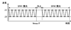
- FIG. 5 is a graph showing an example of periodic wavelength change.
- the horizontal axis indicates time, and the vertical axis indicates wavelength.
- Nmax be the number of pulses of one burst output for exposing one scan field SF#1 or SF#2. Assuming that the repetition frequency of the pulsed laser light is F, the required time for one burst output is Nmax/F.
- the wavelength periodically fluctuates every four pulses between the target wavelengths ⁇ 1 and ⁇ 2.
- the wavelengths of the first and fourth pulsed laser beams are set to the target wavelength ⁇ 1, and the wavelengths of the second and third pulsed laser beams are set to the target wavelength ⁇ 2.
- the laser device 100 outputs pulsed laser light containing a plurality of pulses while periodically varying the wavelength.
- FIG. 6 is a flowchart showing processing for outputting pulsed laser light executed by the laser control processor 130 in the comparative example.
- the voltage command value HVc received from the exposure control processor 210 is used as it is to output pulsed laser light, as will be described below.
- the laser control processor 130 acquires the voltage command value HVc by receiving the voltage command value HVc from the exposure control processor 210 of the exposure apparatus 200 .
- the laser control processor 130 sets the voltage command value HVc to the charger 12 .
- the laser control processor 130 determines whether or not a trigger signal has been received from the exposure control processor 210 . If no trigger signal has been received (S18: NO), laser control processor 130 waits until it receives a trigger signal. If the trigger signal has been received (S18: YES), the laser control processor 130 proceeds to S19.
- the laser control processor 130 causes the laser device 100 to output pulse laser light by transmitting an oscillation trigger signal based on the trigger signal to the pulse power module 13 . After S19, the laser control processor 130 returns the process to S11 and repeats the output of the pulsed laser light by repeating the processes from S11 to S19.
- FIG. 7 is a flowchart showing laser control processing executed by the exposure control processor 210 in the comparative example.
- the exposure control processor 210 determines the voltage command value HVc so that the pulse energy En of the pulse laser light approaches the target pulse energy Et as follows.
- the exposure control processor 210 transmits the voltage command value HVc to the laser control processor 130 of the laser device 100.
- the exposure control processor 210 transmits the voltage command value HVc calculated based on the target pulse energy Et. If the voltage command value HVc is transmitted for the second time or later, the exposure control processor 210 transmits the voltage command value HVc updated in S95.
- the exposure control processor 210 sends a trigger signal to the laser control processor 130 .
- the laser device 100 outputs pulsed laser light.
- the exposure control processor 210 detects the pulse energy En of the pulsed laser light output from the laser device 100 using the energy monitor 220 .
- the exposure control processor 210 converts the difference ⁇ En into a voltage correction amount ⁇ HV using the following equation.
- ⁇ HV ⁇ En/HVep gain
- HVepgain represents the ratio of the amount of change in pulse energy En to the amount of change in voltage command value HVc.
- the exposure control processor 210 updates the voltage command value HVc according to the following formula.
- HVc HVc- ⁇ HV
- the difference ⁇ En and the correction amount ⁇ HV become negative numbers in S93 and S94.
- the correction amount ⁇ HV which is a negative number, is subtracted from the voltage command value HVc to increase the pulse energy En of the next pulse.
- the exposure control processor 210 After S95, the exposure control processor 210 returns the process to S90 and repeats the processes from S90 to S95 to calculate the voltage command value HVc and cause the laser device 100 to output the pulsed laser beam.
- FIG. 8 is a graph showing changes in pulse energy En when pulsed laser light is output while switching between target wavelengths ⁇ 1 and ⁇ 2.
- the horizontal axis of FIG. 8 indicates the pulse number i in the burst output, and the vertical axis indicates the pulse energy En.
- the voltage command value HVc is set to a constant value. Even if the voltage command value HVc is a constant value, the pulse energy En may change. By controlling the voltage command value HVc based on the target pulse energy Et described with reference to FIG. 7, changes in the pulse energy En can be suppressed to some extent.
- the pulse energy En may fluctuate according to the switching of the target wavelengths ⁇ 1 and ⁇ 2 as shown in FIG. be. Vibration of optical components due to high-speed driving of the mirror 63 can be considered as a factor that causes the pulse energy En to fluctuate according to the switching of the target wavelengths ⁇ 1 and ⁇ 2. If the pulse energy En fluctuates frequently, the control described with reference to FIG. 7 may not sufficiently stabilize the pulse energy En.
- the fluctuation of the pulse energy En contains many frequency components corresponding to the reciprocal of the wavelength fluctuation period.
- the reciprocal of the wavelength variation period corresponds to the switching frequency of the target wavelengths ⁇ 1 and ⁇ 2. Therefore, the integrated value of the pulse energy En of the pulsed laser light generated at the target wavelength ⁇ 1 may not match the integrated value of the pulsed energy En of the pulsed laser light generated at the target wavelength ⁇ 2. In this case, the exposure performance may become uneven in the thickness direction of the resist film.
- FIG. 9 schematically shows the configuration of a laser apparatus 100a according to the first embodiment.
- laser control processor 130 includes energy analyzer 133 and voltage correction table 134 .
- the energy analysis unit 133 statistically processes the data of the pulse energy En received from the monitor module 17 to calculate correction data.
- the energy analysis unit 133 may include a control program for performing such statistical processing and calculation of correction data.
- the energy analysis unit 133 may include hardware for performing such statistical processing and calculation of correction data.
- the voltage correction table 134 stores correction data for correcting the voltage command value HVc according to variations in the wavelength of the pulsed laser light.
- the voltage correction table 134 corresponds to the table in this disclosure.
- FIG. 10 is a graph showing correction data included in the voltage correction table 134. As shown in FIG. The horizontal axis of FIG. 10 indicates the pulse number i in the burst output, and the vertical axis indicates the correction value HVtbl included in the correction data. The correction value HVtbl changes according to the switching of the target wavelengths ⁇ 1 and ⁇ 2.
- the voltage correction table 134 may be a table storing the correction value HVtbl for each pulse number i, or may be a function, matrix, or other format. In other respects, the configuration of the first embodiment is the same as the configuration of the comparative example.
- FIG. 11 is a control block diagram of the pulse energy En in the first embodiment.
- the energy control block 210a corresponds to the processing in which the exposure control processor 210 calculates the difference ⁇ En in S93 of FIG.
- the voltage conversion block 210b corresponds to the processing in which the exposure control processor 210 calculates the correction amount ⁇ HV in S94 of FIG. Voltage command value HVc is corrected using this correction amount ⁇ HV.
- the voltage correction block 130a corresponds to processing for correcting the voltage command value HVc received by the laser control processor 130 from the exposure control processor 210 to calculate the voltage setting value HVact. This processing will be described later with reference to FIG.
- the pulsed laser light output block 100b corresponds to processing in which the laser device 100a applies a high voltage to the discharge electrode 11a according to the voltage setting value HVact to output pulsed laser light.
- the pulse energy En of the pulsed laser light is fed back to the above-described processing by the exposure control processor 210 .
- FIG. 12 is a flowchart showing processing for outputting pulsed laser light executed by the laser control processor 130 in the first embodiment.
- the voltage setting value HVact is calculated by correcting the voltage command value HVc received from the exposure control processor 210 as follows.
- the laser control processor 130 determines correction values HVtbl(i) read from the voltage correction table 134 .
- (i) means that it corresponds to the i-th pulse in the burst output.
- the correction value is HVtbl(1).
- the laser control processor 130 corrects the voltage command value HVc according to the following equation using the read correction value HVtbl(i) to calculate the voltage setting value HVact.
- HVact HVc+HVtbl(i)
- the voltage set value HVact corresponds to the corrected voltage command value in the present disclosure.
- the laser control processor 130 sets the voltage setting value HVact to the charger 12 .
- the processes of S18 and S19 are the same as those described with reference to FIG.
- laser control by exposure control processor 210 is similar to that described with reference to FIG.
- FIG. 13 is a flowchart showing update processing of the voltage correction table 134 executed by the laser control processor 130 in the first embodiment.
- the laser control processor 130 determines whether or not the burst output is inactive. For example, when pulsed laser light is not output for one second or longer, it is determined that burst output is inactive. If the burst output is inactive (S20: YES), the laser control processor 130 advances the process to S30.
- the laser control processor 130 updates the correction data contained in the voltage correction table 134.
- the processing of S ⁇ b>30 is performed by the energy analysis unit 133 . Details of S30 will be described later with reference to FIG.
- the laser control processor 130 If the burst output is not on hiatus (S20: NO), or after S30, the laser control processor 130 returns to S20. Through such processing, the laser control processor 130 updates the correction data during the rest period after the end of the first burst output and before the start of the second burst output following the first burst output.
- a period in which the first burst output is performed is an example of a first period in the present disclosure
- a period in which the second burst output is performed is an example of a second period in the present disclosure.
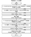
- FIG. 14 is a flowchart showing details of update processing of the voltage correction table 134 in the first embodiment.
- the processing shown in FIG. 14 corresponds to the subroutine of S30 in FIG.
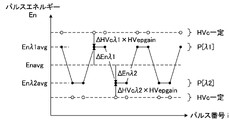
- FIG. 15 is a graph conceptually showing average values Enavg, En ⁇ 1avg, and En ⁇ 2avg and differences ⁇ En ⁇ 1 and ⁇ En ⁇ 2 calculated in FIG.
- the horizontal axis of FIG. 15 indicates the pulse number i in the burst output, and the vertical axis indicates the pulse energy En.
- the laser control processor 130 acquires time-series data of multiple pulse energies En[] in the burst output.
- [ ] means an array, and if the [ ] is blank, it means the entire array corresponding to one burst output.
- the time-series data of the pulse energy En[] corresponds to first time-series data in the present disclosure. As shown in FIG. 15, the pulse energy En may vary depending on the target wavelengths ⁇ 1 and ⁇ 2.
- the laser control processor 130 calculates the average value Enavg of the pulse energies En[].
- the average value Enavg corresponds to the third average value in the present disclosure, and serves as a basis for calculating correction data.
- the laser control processor 130 calculates the average value En ⁇ 1avg of the pulse energy En[ ⁇ 1] at the target wavelength ⁇ 1 and the average value En ⁇ 2avg of the pulse energy En[ ⁇ 2] at the target wavelength ⁇ 2.
- the pulse energy En[ ⁇ 1] means the arrangement of the pulse energies En of the first wavelength pulses P[ ⁇ 1] output according to the target wavelength ⁇ 1 of the pulse energies En[].
- the pulse energy En[ ⁇ 2] means the arrangement of the pulse energies En of the second wavelength pulses P[ ⁇ 2] output according to the target wavelength ⁇ 2.
- the average value En ⁇ 1avg corresponds to the first average value in the present disclosure
- the average value En ⁇ 2avg corresponds to the second average value in the present disclosure.
- laser control processor 130 calculates difference ⁇ En ⁇ 1 between average value En ⁇ 1avg and average value Enavg and difference ⁇ En ⁇ 2 between average value En ⁇ 2avg and average value Enavg using the following equations.
- ⁇ En ⁇ 1 En ⁇ 1avg-Enavg
- ⁇ En ⁇ 2 En ⁇ 2avg-Enavg
- the laser control processor 130 converts the differences ⁇ En ⁇ 1 and ⁇ En ⁇ 2 into voltage correction amounts ⁇ HV ⁇ 1 and ⁇ HV ⁇ 2, respectively, using the following equations.
- ⁇ HV ⁇ 1 ⁇ En ⁇ 1/HVep gain
- ⁇ HV ⁇ 2 ⁇ En ⁇ 2/HVep gain
- the laser control processor 130 calculates the correction values HVtbl[ ⁇ 1] and HVtbl[ ⁇ 2] using the following equations, and updates the correction data contained in the voltage correction table 134.
- HVtbl[ ⁇ 1] HVtbl[ ⁇ 1] ⁇ HV ⁇ 1
- HVtbl[ ⁇ 2] HVtbl[ ⁇ 2] ⁇ HV ⁇ 2
- the correction values HVtbl[ ⁇ 1] and HVtbl[ ⁇ 2] are calculated for each target wavelength.
- the initial values of HVtbl[ ⁇ 1] and HVtbl[ ⁇ 2] may be preset by adjusted light emission (see FIG. 4).
- the correction values HVtbl[ ⁇ 1] and HVtbl[ ⁇ 2] may be calculated using values obtained by multiplying the correction amounts ⁇ HV ⁇ 1 and ⁇ HV ⁇ 2 by coefficients larger than 0 and smaller than 1, respectively.
- All the calculated correction values HVtbl[ ⁇ 1] are arrays of the same value.
- the correction values HVtbl[ ⁇ 2] are all arrayed with the same value.
- the present disclosure is not limited to this, and the correction values HVtbl[ ⁇ 1] and HVtbl[ ⁇ 2] may be changed in one burst output.
- the correction values HVtbl[ ⁇ 1] and HVtbl[ ⁇ 2] may be calculated using values obtained by multiplying the correction amounts ⁇ HV ⁇ 1 and ⁇ HV ⁇ 2 by a function of time.
- the correction data including the correction values HVtbl[ ⁇ 1] and HVtbl[ ⁇ 2] are calculated using the time-series data of the pulse energy En[] in the first burst output.
- the correction data is stored in voltage correction table 134 .
- the voltage command value HVc is corrected using the correction data read from the voltage correction table 134 by the processing of S16a in FIG.
- the overall average of the correction values HVtbl[ ⁇ 1] and HVtbl[ ⁇ 2] may be set to 0 so that the integrated value of the pulse energy En[] does not change even if the voltage command value HVc is corrected (see FIG. 10).
- the voltage command value HVc is corrected using the time-series data of the pulse energies En[ ] of a plurality of pulses output while periodically varying the wavelength. Calculate the data. According to this, the voltage command value HVc can be corrected so as to suppress variations in the pulse energy En that accompany wavelength variations.
- the correction data is calculated before the start of the period in which the second burst output next to the first burst output is performed. do. According to this, the voltage command value HVc can be corrected using the latest data for each burst output.
- the correction data is stored in the voltage correction table 134, and the voltage command value HVc is corrected using the correction data read from the voltage correction table 134.
- FIG. By using the voltage correction table 134, the voltage command value HVc can be corrected at high speed.
- the correction data is calculated based on the average value Enavg of the pulse energies En[ ]. According to this, even if the target pulse energy Et set in the exposure apparatus 200 is unknown, the voltage command value HVc can be appropriately corrected based on the average value Enavg.
- An average value Enavg is calculated.
- the correction data is calculated using the difference ⁇ En ⁇ 1 between the average value En ⁇ 1avg and the average value Enavg and the difference ⁇ En ⁇ 2 between the average value En ⁇ 2avg and the average value Enavg.
- the integrated value of the pulse energy En[ ⁇ 1] at the target wavelength ⁇ 1 and the integrated value of the pulse energy En[ ⁇ 2] at the target wavelength ⁇ 2 can be made close to each other. Thereby, the exposure performance can be made uniform in the thickness direction of the resist film.
- the correction values HVtbl[ ⁇ 1] and HVtbl[ ⁇ 2] are calculated for each target wavelength set during the period in which the first burst output is performed. According to this, the correction data including the correction values HVtbl[ ⁇ 1] and HVtbl[ ⁇ 2] can be calculated at high speed. Otherwise, the first embodiment is the same as the comparative example.
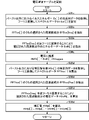
- FIG. 16 shows details of update processing of the voltage correction table 134 in the second embodiment. It is a flow chart showing. The processing shown in FIG. 16 corresponds to the subroutine of S30 in FIG.
- FIG. 17 is a graph conceptually showing average values HVcavg, HVc ⁇ 1avg, and HVc ⁇ 2avg calculated in FIG. 16, and differences ⁇ HVc ⁇ 1 and ⁇ HVc ⁇ 2.
- the horizontal axis of FIG. 17 indicates the pulse number i in the burst output, and the vertical axis indicates the voltage command value HVc.
- FIG. 18 is a graph conceptually showing average values Enavg, En ⁇ 1avg, and En ⁇ 2avg and differences ⁇ En ⁇ 1 and ⁇ En ⁇ 2 calculated in FIG.
- the horizontal axis of FIG. 18 indicates the pulse number i in the burst output, and the vertical axis indicates the pulse energy En.
- the laser control processor 130 acquires time-series data of multiple voltage command values HVc[] in the burst output.
- the time-series data of the voltage command value HVc[] corresponds to second time-series data in the present disclosure.
- the laser control processor 130 calculates the average value HVcavg of the voltage command values HVc[].
- the average value HVcavg corresponds to the sixth average value in the present disclosure, and serves as a reference for calculating correction data.
- the laser control processor 130 calculates the average value HVc ⁇ 1avg of the voltage command values HVc[ ⁇ 1] at the target wavelength ⁇ 1 and the average value HVc ⁇ 2avg of the voltage command values HVc[ ⁇ 2] at the target wavelength ⁇ 2.
- the voltage command value HVc[ ⁇ 1] means the arrangement of the voltage command values HVc when outputting the first wavelength pulse P[ ⁇ 1] according to the target wavelength ⁇ 1 of the voltage command values HVc[].
- the voltage command value HVc[ ⁇ 2] means the arrangement of the voltage command values HVc when outputting the second wavelength pulse P[ ⁇ 2] according to the target wavelength ⁇ 2.
- the average value HVc ⁇ 1avg corresponds to the fourth average value in the present disclosure
- the average value HVc ⁇ 2avg corresponds to the fifth average value in the present disclosure.
- laser control processor 130 calculates difference ⁇ HVc ⁇ 1 between average value HVc ⁇ 1avg and average value HVcavg and difference ⁇ HVc ⁇ 2 between average value HVc ⁇ 2avg and average value HVcavg using the following equations.
- ⁇ HVc ⁇ 1 HVc ⁇ 1avg-HVcavg
- ⁇ HVc ⁇ 2 HVc ⁇ 2avg ⁇ HVcavg
- the laser control processor 130 calculates the correction values HVtbl[ ⁇ 1] and HVtbl[ ⁇ 2] using the following formulas, and updates the correction data contained in the voltage correction table 134.
- HVtbl[ ⁇ 1] HVtbl[ ⁇ 1] ⁇ ( ⁇ HV ⁇ 1 ⁇ HVc ⁇ 1)
- HVtbl[ ⁇ 2] HVtbl[ ⁇ 2] ⁇ ( ⁇ HV ⁇ 2 ⁇ HVc ⁇ 2)
- the pulse energy En increases by ⁇ HVc ⁇ 2 ⁇ HVepgain when the target wavelength ⁇ 2 is set, compared to when the voltage command value HVc is constant. Therefore, the pulse energy En can be further stabilized by not only correcting based on the difference ⁇ En ⁇ 2, but also correcting using the time-series data of the voltage command value HVc[ ].
- the correction value HVtbl[ ⁇ 1] may be calculated using a value obtained by multiplying the correction amounts ⁇ HV ⁇ 1 and ⁇ HVc ⁇ 1 by a coefficient larger than 0 and smaller than 1.
- the correction value HVtbl[ ⁇ 2] may be calculated using a value obtained by multiplying the correction amounts ⁇ HV ⁇ 2 and ⁇ HVc ⁇ 2 by a coefficient larger than 0 and smaller than 1.
- the correction data is calculated using the time-series data of the plurality of voltage command values HVc[ ] set during the period in which the first burst output is performed. According to this, the variation of the voltage command value HVc set by the exposure apparatus 200 is also corrected, and the correction can be performed more appropriately.
- the correction data is calculated based on the average value HVcavg of the voltage command values HVc[ ]. According to this, even if the target pulse energy Et set in the exposure apparatus 200 is unknown, it can be appropriately corrected using the average value HVcavg as a reference.
- the average value HVc ⁇ 1avg of the voltage command value HVc[ ⁇ 1] when the target wavelength ⁇ 1 is set and the voltage command value HVc[ ⁇ 2] when the target wavelength ⁇ 2 is set and the average value HVcavg of the voltage command value HVc[ ] are calculated.
- the correction data is calculated using the difference ⁇ HVc ⁇ 1 between the average value HVc ⁇ 1avg and the average value HVcavg and the difference ⁇ HVc ⁇ 2 between the average value HVc ⁇ 2avg and the average value HVcavg.
- the variation in the voltage command value HVc set by the exposure apparatus 200 is also corrected, and the integrated value of the pulse energy En[ ⁇ 1] at the target wavelength ⁇ 1 and the pulse energy En[ ⁇ 2 at the target wavelength ⁇ 2 ] can be brought close to each other.
- the second embodiment is the same as the first embodiment.
- FIG. 19 shows details of update processing of the voltage correction table 134 in the third embodiment. It is a flow chart showing. The processing shown in FIG. 19 corresponds to the subroutine of S30 in FIG.
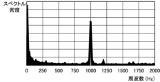
- FIG. 20 is a graph of spectrum data FFTen[ ] obtained by Fourier transforming the time-series data of the pulse energy En[ ] in FIG. 19 .
- the horizontal axis of FIG. 20 indicates frequency, and the vertical axis indicates spectral density.
- the laser control processor 130 acquires time-series data of pulse energies En[] of multiple pulses in the burst output.
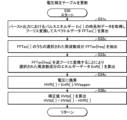
- the laser control processor 130 Fourier-transforms the time-series data of the pulse energy En[] to calculate the spectral data FFTen[].
- Fourier transform processing can be performed by fast Fourier transform. As shown in FIG. 20, the spectral data FFTen[] obtained by Fourier transforming the time-series data of the pulse energy En[] of the pulsed laser light output by periodically varying the wavelength is obtained at a specific frequency. have a peak. This frequency corresponds to the reciprocal of the wavelength fluctuation period.
- the laser control processor 130 extracts the selected frequency component FFTen[freq] from the spectral data FFTen[].
- the frequency component FFTen[freq] corresponding to the reciprocal of the wavelength fluctuation period is selected.
- a frequency component of 1000 Hz is selected.
- a frequency band including the peak of the spectrum data FFTen[ ] and its surrounding frequencies may be selected.
- the spectrum data FFTen[ ] includes multiple peaks, multiple frequency components corresponding to those peaks may be selected.
- the laser control processor 130 calculates energy data Enfft[] of the selected frequency by inverse Fourier transforming the frequency component FFTen[freq].
- the energy data Enfft[] contains the energy amplitude for each pulse.
- the inverse Fourier transform process can be performed by a fast inverse Fourier transform.
- the laser control processor 130 converts the energy data Enfft[ ] into a voltage correction amount HVfft[ ] according to the following equation.
- HVfft[ ] Enfft[ ]/HVepgain
- the laser control processor 130 calculates the correction value HVtbl[ ] using the following formula, and updates the correction data contained in the voltage correction table 134.
- HVtbl[ ] HVtbl[ ] ⁇ HVfft[ ]
- the correction value HVtbl[ ] is calculated for each individual pulse in the burst output.
- the initial value of the correction value HVtbl[ ] may be set in advance by adjusting light emission (see FIG. 4).
- the correction value HVtbl[] may be calculated using a value obtained by multiplying the correction amount HVfft[] by a coefficient greater than 0 and less than 1.
- the frequency component selected from the time-series data of the pulse energies En[ ] of the plurality of pulses output during the period in which the first burst output is performed is Extract and calculate correction data. According to this, the variation of the selected frequency component of the pulse energy En can be reduced, and the pulse energy En can be stabilized.
- the selected frequency component is a frequency component corresponding to the reciprocal of the wavelength fluctuation period when the pulsed laser light is output during the period in which the first burst output is performed. . According to this, the fluctuation of the frequency component corresponding to the switching frequency of the target wavelengths ⁇ 1 and ⁇ 2 can be reduced, and the pulse energy En can be stabilized.
- the spectral data FFTen[ ] are calculated by Fourier transforming the time-series data of the pulse energy En[ ].
- Energy data Enfft[ ] is calculated by performing an inverse Fourier transform on the frequency component FFTen[freq] selected from the spectrum data FFTen[ ].
- Correction data is calculated using this energy data Enfft[ ]. According to this, the correction data corresponding to the phase shift between the switching of the target wavelengths ⁇ 1 and ⁇ 2 and the fluctuation of the pulse energy En is calculated, so that the pulse energy En can be stabilized further.
- the correction value HVtbl[ ] is calculated for each individual pulse output during the period in which the first burst output is performed. According to this, an appropriate correction value HVtbl[ ] can be calculated for each pulse. Otherwise, the third embodiment is the same as the first embodiment.
- FIG. 21 It is a flow chart which shows details. The processing shown in FIG. 21 corresponds to the subroutine of S30 in FIG.
- the laser control processor 130 acquires time-series data of multiple voltage command values HVc[] in the burst output.
- the laser control processor 130 Fourier-transforms the time-series data of the voltage command value HVc[] to calculate spectrum data FFThvc[]. Fourier transform processing can be performed by fast Fourier transform.
- the laser control processor 130 extracts the selected frequency component FFThvc[freq] from the spectrum data FFThvc[].
- the frequency of the frequency component FFThvc[freq] may be the same as the frequency of the frequency component FFTen[freq] selected in S32c.
- the laser control processor 130 calculates the voltage data HVcfft[] of the selected frequency by inverse Fourier transforming the frequency component FFThvc[freq].
- the voltage data HVcfft[] contains the voltage amplitude for each pulse.
- the inverse Fourier transform process can be performed by a fast inverse Fourier transform.
- the laser control processor 130 calculates the correction value HVtbl[ ] using the following formula, and updates the correction data contained in the voltage correction table 134.
- HVtbl[ ] HVtbl[ ]-(HVfft[ ]-HVcfft[ ])
- the correction value HVtbl[] may be calculated using a value obtained by multiplying the correction amounts HVfft[] and HVcfft[] by a coefficient greater than 0 and less than 1.
- the selected frequency component is extracted from the time-series data of the plurality of voltage command values HVc[ ] set during the period in which the first burst output is performed. and calculate the correction data.
- the time-series data of the voltage command value HVc[ ] it is possible to correct the variation of the voltage command value HVc set by the exposure apparatus 200 and perform the correction more appropriately.
- the spectrum data FFThvc[ ] is calculated by Fourier transforming the time-series data of the voltage command value HVc[ ].
- Voltage data HVcfft[ ] is calculated by inverse Fourier transforming the frequency component FFThvc[freq] selected from the spectrum data FFThvc[ ].
- Correction data is calculated using this voltage data HVcfft[ ]. According to this, since the correction data corresponding to the phase shift between the switching of the target wavelengths ⁇ 1 and ⁇ 2 and the variation of the voltage command value HVc is calculated, the pulse energy En can be further stabilized. Otherwise, the fourth embodiment is the same as the third embodiment.
- FIG. 22 is a flowchart showing details of update processing of the voltage correction table 134 in the fifth embodiment. be.
- the processing shown in FIG. 22 corresponds to the subroutine of S30 in FIG.
- FIG. 23 is a graph showing periodically changing wavelengths.
- the horizontal axis of FIG. 23 indicates the pulse number i in the burst output, and the vertical axis indicates the wavelength.
- the pulse number j within the wavelength variation period indicates the number of the pulse within the wavelength variation period. For example, if the number of pulses in one cycle is 4, j is an integer from 1 to 4.
- the laser control processor 130 calculates the average value En#javg of the pulse energy En[#j] for each pulse number j within the wavelength variation period.
- Pulse energy En[#j] means an array of pulse energies En of pulse number j among pulse energies En[]. For example, if the value of j is 1, the pulse with the pulse number j corresponds to the pulse with the pulse number i of 1, 5, 9, . These correspond to pulses with pulse numbers i of 2, 6, 10, . . .
- the average value En#javg is expressed as En#1avg, and if the value of j is 2, it is expressed as En#2avg.
- the average value En#1avg corresponds to the seventh average value in the present disclosure.
- the average value En#2avg corresponds to the eighth average value in the present disclosure.
- the number of average values En#javg corresponds to the maximum value of j.
- the correction value HVtbl[#j] may be calculated using the correction amount ⁇ HV#j as in the first embodiment. However, when the voltage command value HVc is controlled so that the pulse energy En approaches the target pulse energy Et as described with reference to FIG. 7, as shown in FIG. A frequency component corresponding to the reciprocal of the fluctuation period may be included. As described in the second embodiment, in order to further stabilize the pulse energy En, it is desirable to correct the variation of the voltage command value HVc as well.
- the laser control processor 130 calculates the average value HVc#javg of the voltage command values HVc[#j] for each pulse number j within the wavelength variation period.
- the voltage command value HVc[#j] means an array of the voltage command values HVc of the pulse with the pulse number j among the voltage command values HVc[]. For example, if the value of j is 1, the average value HVc#javg is expressed as HVc#1avg, and if the value of j is 2, it is expressed as HVc#2avg.
- the average value HVc#1avg corresponds to the tenth average value in the present disclosure
- the average value HVc#2avg corresponds to the eleventh average value in the present disclosure
- the number of average values HVc#javg corresponds to the maximum value of j.
- the laser control processor 130 calculates the correction value HVtbl[#j] using the following formula, and updates the correction data contained in the voltage correction table 134.
- HVtbl[#j] HVtbl[#j]-( ⁇ HV#j- ⁇ HVc#j)
- the correction value HVtbl[#j] is calculated for each pulse number j within the wavelength variation period.
- the initial value of HVtbl[#j] may be set in advance by adjusted light emission (see FIG. 4).
- the correction value HVtbl[#j] may be calculated using a value obtained by multiplying the correction amounts ⁇ HV#j and ⁇ HVc#j by a coefficient larger than 0 and smaller than 1.
- the calculated correction value HVtbl[#j] is an array of the same values for the same pulse number j.
- the present disclosure is not limited to this, and the correction value HVtbl[#j] may be changed in one burst output.
- the correction value HVtbl[#j] may be calculated using a value obtained by multiplying the correction amounts ⁇ HV#j and ⁇ HVc#j by a function of time.
- An average value En#2avg of the pulse energy En[#2] and an average value Enavg of the pulse energy En[ ] of the pulse are calculated.
- the correction data is calculated using the difference ⁇ En#1 between the average value En#1avg and the average value Enavg and the difference ⁇ En#2 between the average value En#2avg and the average value Enavg. According to this, the correction data corresponding to the phase shift between the switching of the target wavelengths ⁇ 1 and ⁇ 2 and the fluctuation of the pulse energy En is calculated, so that the pulse energy En can be stabilized further.
- the correction value HVtbl[#j] is calculated for each pulse number j within the wavelength fluctuation period when the pulsed laser light is output during the period in which the first burst output is performed. do. According to this, the correction data including the correction value HVtbl[#j] can be calculated at high speed.
- the average value HVc#1avg of the voltage command value HVc[#1] when the pulse number j within the wavelength variation period is 1 and when the pulse number j is 2
- An average value HVc#2avg of the voltage command values HVc[#2] and an average value HVcavg of the voltage command values HVc[ ] are calculated.
- the correction data is calculated using the difference ⁇ HVc#1 between the average value HVc#1avg and the average value HVcavg and the difference ⁇ HVc#2 between the average value HVc#2avg and the average value HVcavg.
- the pulse energy En can be further stabilized.
- the fifth embodiment is the same as the second embodiment.
- FIG. 3 is a flowchart showing the processing of .
- the voltage command value HVc is obtained by the laser control processor 130 calculating the voltage command value HVc based on the target pulse energy Et received from the exposure control processor 210 as follows.
- the configuration of the sixth embodiment may be the same as that of the first embodiment.
- the monitor module 17 measures not only the wavelength of the pulse laser light but also the pulse energy En.
- the laser control processor 130 receives the target pulse energy Et from the exposure control processor 210.
- the target pulse energy Et may not be received for each pulse, but may be received for each burst output, for example.
- the laser control processor 130 uses the monitor module 17 to detect the pulse energy En of the pulsed laser light.
- the laser control processor 130 updates the voltage command value HVc according to the following equation.
- HVc HVc- ⁇ HV
- the difference ⁇ En and the correction amount ⁇ HV are negative numbers in S13f and S14f.
- the pulse energy En of the next pulse increases.
- FIG. 25 is a flowchart showing laser control processing executed by the exposure control processor 210 in the sixth embodiment.
- the exposure control processor 210 does not determine the voltage command value HVc.
- the exposure control processor 210 transmits the target pulse energy Et to the laser control processor 130 of the laser device 100a.
- the target pulse energy Et may not be transmitted for each pulse, but may be transmitted for each burst output, for example.
- the processing of S91 is the same as that described with reference to FIG.
- the exposure control processor 210 causes the laser device 100a to output a pulsed laser beam by repeating the process of S91.
- the sixth embodiment is the same as any one of the first to fifth embodiments.
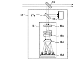
- FIG. 26 schematically shows the configuration of the monitor module 17 used in the comparative example and the first to sixth embodiments.
- the monitor module 17 includes a beam splitter 17a, an energy sensor 17b, and an etalon spectroscope 18.
- the beam splitter 17 a is located in the optical path of the pulsed laser beam reflected by the beam splitter 16 .
- the energy sensor 17b is positioned in the optical path of the pulsed laser beam reflected by the beam splitter 17a.
- the etalon spectroscope 18 is arranged in the optical path of the pulsed laser beam that has passed through the beam splitter 17a.
- the etalon spectroscope 18 includes a diffuser plate 18a, an etalon 18b, a condenser lens 18c, and a line sensor 18d.
- the diffusion plate 18a is positioned on the optical path of the pulsed laser beam transmitted through the beam splitter 17a.
- the diffusion plate 18a has a large number of irregularities on its surface, and is configured to transmit and diffuse the pulsed laser beam.
- the etalon 18b is positioned in the optical path of the pulsed laser beam transmitted through the diffuser plate 18a.
- Etalon 18b includes two partially reflective mirrors. The two partially reflecting mirrors face each other with an air gap of a predetermined distance, and are bonded together via spacers.
- the condenser lens 18c is positioned on the optical path of the pulsed laser beam that has passed through the etalon 18b.
- the line sensor 18d is located on the focal plane of the condenser lens 18c along the optical path of the pulsed laser beam that has passed through the condenser lens 18c.
- the line sensor 18d receives interference fringes formed by the etalon 18b and the condenser lens 18c.
- An interference fringe is an interference pattern of pulsed laser light and has a shape of concentric circles, and the square of the distance from the center of the concentric circles is proportional to the change in wavelength.
- the line sensor 18d is a light distribution sensor including a large number of light receiving elements arranged one-dimensionally.
- an image sensor including a large number of light receiving elements arranged two-dimensionally may be used as the light distribution sensor.
- Each light receiving element is called a channel.
- a light intensity distribution of interference fringes is obtained from the light intensity detected in each channel.
- the energy sensor 17 b detects the pulse energy En of the pulsed laser light and outputs data on the pulse energy En to the laser control processor 130 .
- Data on the pulse energy En may be used by the laser control processor 130 to feedback-control the voltage command value HVc in the sixth embodiment.
- the timing at which the data on the pulse energy En is received can be used as a reference for the timing at which the laser control processor 130 outputs a data output trigger to the etalon spectroscope 18 .
- the etalon spectroscope 18 generates a measurement waveform from the interference pattern of the pulsed laser light detected by the line sensor 18d.
- the etalon spectroscope 18 transmits the measured waveform to the laser control processor 130 according to the data output trigger output from the laser control processor 130 .
- the measured waveform is also called a fringe waveform, and indicates the relationship between the distance from the center of the concentric circles forming the interference fringes and the light intensity.
- the laser control processor 130 uses the measurement waveform output from the etalon spectroscope 18 to calculate the central wavelength of the pulsed laser light as the measurement wavelength.
- a controller (not shown) included in the etalon spectroscope 18 calculates the measurement wavelength and transmits it to the laser control processor 130 .
- the laser control processor 130 feedback-controls the central wavelength of the pulsed laser light by outputting control signals to drivers (not shown) of the rotary stages 143 and 163 based on the target wavelengths ⁇ 1 and ⁇ 2 and the measurement wavelength.
Landscapes
- Physics & Mathematics (AREA)
- Electromagnetism (AREA)
- Engineering & Computer Science (AREA)
- Plasma & Fusion (AREA)
- Optics & Photonics (AREA)
- General Physics & Mathematics (AREA)
- Lasers (AREA)
- Exposure And Positioning Against Photoresist Photosensitive Materials (AREA)
Abstract
Description
1.比較例
1.1 露光システム
1.1.1 構成
1.1.2 動作
1.2 レーザ装置100
1.2.1 構成
1.2.2 動作
1.3 狭帯域化モジュール14
1.3.1 構成
1.3.2 動作
1.4 ステップアンドスキャン露光
1.5 周期的な波長変化の例
1.6 パルスレーザ光の出力制御
1.6.1 レーザ制御プロセッサ130による制御
1.6.2 露光制御プロセッサ210によるレーザ制御
1.7 比較例の課題
2.パルスエネルギーEn[ ]の時系列データを用いて補正データを算出するレーザ装置
2.1 構成
2.2 制御ブロック図
2.3 パルスレーザ光の出力制御
2.4 電圧補正テーブル134の更新タイミング
2.5 電圧補正テーブル134の更新処理
2.6 作用
3.電圧指令値HVc[ ]の時系列データをさらに用いて補正データを算出するレーザ装置
3.1 電圧補正テーブル134の更新処理
3.2 作用
4.パルスエネルギーEn[ ]の時系列データをフーリエ変換して補正データを算出するレーザ装置
4.1 電圧補正テーブル134の更新処理
4.2 作用
5.電圧指令値HVc[ ]の時系列データをフーリエ変換して補正データを算出するレーザ装置
5.1 電圧補正テーブル134の更新処理
5.2 作用
6.波長変動周期内のパルス番号jごとに補正データを算出するレーザ装置
6.1 電圧補正テーブル134の更新処理
6.2 作用
7.目標パルスエネルギーEtに基づいて電圧指令値HVcを設定するレーザ装置
7.1 レーザ制御プロセッサ130による制御
7.2 露光制御プロセッサ210による制御
8.その他
8.1 モニタモジュール17の構成
8.2 モニタモジュール17の動作
8.3 補足
1.1 露光システム
図1は、比較例における露光システムの構成を概略的に示す。本開示の比較例とは、出願人のみによって知られていると出願人が認識している形態であって、出願人が自認している公知例ではない。
露光システムは、レーザ装置100と、露光装置200と、を含む。図1においてはレーザ装置100が簡略化して示されている。
図1に示されるように、露光装置200は、照明光学系201と、投影光学系202と、露光制御プロセッサ210と、を含む。
投影光学系202は、レチクルを透過したパルスレーザ光を、縮小投影してワークピーステーブルWT上に配置された図示しないワークピースに結像させる。ワークピースはレジスト膜が塗布された半導体ウエハ等の感光基板である。
露光制御プロセッサ210は、目標波長λ1及びλ2と電圧指令値HVcとを含む各種パラメータと、トリガ信号と、をレーザ制御プロセッサ130に送信する。レーザ制御プロセッサ130は、これらのパラメータ及び信号に従ってレーザ装置100を制御する。目標波長λ1及びλ2は波長の目標値であって、目標波長λ1は本開示における第1の目標波長に相当し、目標波長λ2は本開示における第2の目標波長に相当する。目標波長λ1は目標波長λ2より大きい波長とする。
このような露光工程によって半導体ウエハにレチクルパターンが転写される。その後、複数の工程を経ることで電子デバイスを製造することができる。
1.2.1 構成
図2は、比較例におけるレーザ装置100の構成を概略的に示す。図2においては露光装置200に含まれる幾つかの要素の図示が省略されている。
レーザチャンバ10は、放電電極11a及びこれと対をなす図示しない放電電極を内部に備えている。図示しない放電電極は、図2の紙面に垂直な方向において放電電極11aと重なるように位置している。レーザチャンバ10には、例えばレアガスとしてアルゴンガス又はクリプトンガス、ハロゲンガスとしてフッ素ガス、バッファガスとしてネオンガス等を含むレーザガスが封入される。
出力結合ミラー15は、部分反射ミラーで構成されている。
レーザ制御プロセッサ130は、露光制御プロセッサ210から目標波長λ1及びλ2と、電圧指令値HVcと、を含む各種パラメータを取得する。レーザ制御プロセッサ130は、目標波長λ1及びλ2に基づいて狭帯域化モジュール14に制御信号を送信する。レーザ制御プロセッサ130は、取得した電圧指令値HVcを充電器12に設定する。
1.3.1 構成
プリズム41、42、及び43は、ウインドウ10aから出射した光ビームの光路にこの順で配置されている。プリズム41~43は、光ビームが入出射するプリズム41~43の表面がいずれもV軸に平行となるように配置され、それぞれ図示しないホルダによって支持されている。プリズム43は、回転ステージ143によってV軸に平行な軸周りに回転可能となっている。回転ステージ143の例としては、ステッピングモータを備えた可動範囲の大きい回転ステージが挙げられる。
グレーティング53は、図示しないホルダによって支持されている。
ウインドウ10aから出射した光ビームは、プリズム41~43の各々によって、V軸に垂直な面であるHZ面に平行な面内で進行方向を変えられ、HZ面に平行な面内でビーム幅を拡大させられる。
プリズム41~43を透過した光ビームは、ミラー63によって反射されてグレーティング53に入射する。
図3は、露光システムによって露光される半導体ウエハWF#1の例を示す。半導体ウエハWF#1は、例えば、ほぼ円板形を有する単結晶シリコンの板である。半導体ウエハWF#1には例えば感光性のレジスト膜が塗布されている。半導体ウエハWF#1の露光は、スキャンフィールドSF#1、SF#2等の区画ごとに行われる。スキャンフィールドSF#1、SF#2の各々は、1枚のレチクルのレチクルパターンが転写される領域に相当する。1つめのスキャンフィールドSF#1にパルスレーザ光が照射されるように半導体ウエハWF#1を移動させて、スキャンフィールドSF#1を露光する。その後、2つめのスキャンフィールドSF#2にパルスレーザ光が照射されるように半導体ウエハWF#1を移動させて、スキャンフィールドSF#2を露光する。その後同様に半導体ウエハWF#1を移動させながら最後のスキャンフィールドSF#maxまでの露光を行う。
図5は、波長の周期的な変動の例を示すグラフである。図5において、横軸は時間を示し、縦軸は波長を示す。
1つのスキャンフィールドSF#1又はSF#2を露光するための1回のバースト出力のパルス数をNmaxとする。パルスレーザ光の繰り返し周波数をFとすると、1回のバースト出力の所要時間はNmax/Fである。
1.6.1 レーザ制御プロセッサ130による制御
図6は、比較例においてレーザ制御プロセッサ130によって実行されるパルスレーザ光の出力のための処理を示すフローチャートである。比較例においては、以下に説明するように露光制御プロセッサ210から受信する電圧指令値HVcをそのまま用いてパルスレーザ光が出力される。
S19の後、レーザ制御プロセッサ130はS11に処理を戻し、S11からS19までの処理を繰り返すことにより、パルスレーザ光の出力を繰り返す。
図7は、比較例において露光制御プロセッサ210によって実行されるレーザ制御の処理を示すフローチャートである。露光制御プロセッサ210は、以下のようにパルスレーザ光のパルスエネルギーEnが目標パルスエネルギーEtに近づくように電圧指令値HVcを決定する。
S92において、露光制御プロセッサ210は、レーザ装置100から出力されたパルスレーザ光のパルスエネルギーEnをエネルギーモニタ220により検出する。
ΔEn=En-Et
目標パルスエネルギーEtとしては、1回のバースト出力においては一定の値が設定される。
ΔHV=ΔEn/HVepgain
ここで、HVepgainは電圧指令値HVcの変化量に対するパルスエネルギーEnの変化量の比を示す。
HVc=HVc-ΔHV
例えば、S92で検出されたパルスエネルギーEnが目標パルスエネルギーEtより小さかった場合は、S93及びS94において差ΔEn及び補正量ΔHVが負数となる。この場合、S95においては電圧指令値HVcから負数である補正量ΔHVが減算され、次のパルスのパルスエネルギーEnが大きくなる。
図8は、目標波長λ1及びλ2を切り替えながらパルスレーザ光を出力したときのパルスエネルギーEnの変化を示すグラフである。図8の横軸はバースト出力におけるパルス番号iを示し、縦軸はパルスエネルギーEnを示す。電圧指令値HVcは一定の値としている。電圧指令値HVcが一定の値であってもパルスエネルギーEnが変化することがある。図7を参照しながら説明した目標パルスエネルギーEtに基づく電圧指令値HVcの制御によって、パルスエネルギーEnの変化はある程度抑制することができる。
2.1 構成
図9は、第1の実施形態におけるレーザ装置100aの構成を概略的に示す。第1の実施形態において、レーザ制御プロセッサ130は、エネルギー解析部133と電圧補正テーブル134とを含む。
その他の点については、第1の実施形態の構成は、比較例の構成と同様である。
図11は、第1の実施形態におけるパルスエネルギーEnの制御ブロック図である。
エネルギー制御ブロック210aは、図7のS93において露光制御プロセッサ210が差ΔEnを算出する処理に相当する。
図12は、第1の実施形態においてレーザ制御プロセッサ130によって実行されるパルスレーザ光の出力のための処理を示すフローチャートである。第1の実施形態においては、以下のように露光制御プロセッサ210から受信する電圧指令値HVcを補正して電圧設定値HVactを算出する。
S16aにおいて、レーザ制御プロセッサ130は、電圧補正テーブル134から読み出す補正値HVtbl(i)を決定する。(i)はバースト出力におけるi番目のパルスに相当することを意味する。例えば、バースト出力における1番目のパルスの電圧指令値HVcを補正する場合に、補正値はHVtbl(1)である。レーザ制御プロセッサ130は、読み出された補正値HVtbl(i)を用いて以下の式により電圧指令値HVcを補正し、電圧設定値HVactを算出する。
HVact=HVc+HVtbl(i)
電圧設定値HVactは、本開示における補正された電圧指令値に相当する。
S18及びS19の処理は図6を参照しながら説明したものと同様である。
第1の実施形態において、露光制御プロセッサ210によるレーザ制御は図7を参照しながら説明したものと同様である。
図13は、第1の実施形態においてレーザ制御プロセッサ130によって実行される電圧補正テーブル134の更新処理を示すフローチャートである。
このような処理により、レーザ制御プロセッサ130は第1のバースト出力の終了後、第1のバースト出力の次の第2のバースト出力の開始前の休止期間において補正データを更新する。第1のバースト出力が行われる期間は本開示における第1の期間の一例であり、第2のバースト出力が行われる期間は本開示における第2の期間の一例である。
図14は、第1の実施形態における電圧補正テーブル134の更新処理の詳細を示すフローチャートである。図14に示される処理は、図13のS30のサブルーチンに相当する。図15は、図14において算出される平均値Enavg、Enλ1avg、及びEnλ2avgと、差ΔEnλ1及びΔEnλ2とを概念的に示すグラフである。図15の横軸はバースト出力におけるパルス番号iを示し、縦軸はパルスエネルギーEnを示す。
ΔEnλ1=Enλ1avg-Enavg
ΔEnλ2=Enλ2avg-Enavg
ΔHVλ1=ΔEnλ1/HVepgain
ΔHVλ2=ΔEnλ2/HVepgain
HVtbl[λ1]=HVtbl[λ1]-ΔHVλ1
HVtbl[λ2]=HVtbl[λ2]-ΔHVλ2
このように、補正値HVtbl[λ1]及びHVtbl[λ2]は目標波長ごとに算出される。ここで、HVtbl[λ1]及びHVtbl[λ2]の初期値は、調整発光(図4参照)によって予め設定されてもよい。
但し、本開示はこれに限定されず、1回のバースト出力において補正値HVtbl[λ1]及びHVtbl[λ2]がそれぞれ変化するようにしてもよい。例えば、補正量ΔHVλ1及びΔHVλ2に時間の関数を乗算して得られた値を用いて補正値HVtbl[λ1]及びHVtbl[λ2]を算出してもよい。
(1)第1の実施形態によれば、波長を周期的に変動させながら出力された複数のパルスのパルスエネルギーEn[ ]の時系列データを用いて、電圧指令値HVcの補正データを算出する。
これによれば、波長の変動に伴うパルスエネルギーEnの変動を抑制するように、電圧指令値HVcを補正することができる。
これによれば、バースト出力ごとに最新のデータを用いて電圧指令値HVcを補正できる。
電圧補正テーブル134を用いることで、電圧指令値HVcの補正を高速に行うことができる。
これによれば、露光装置200において設定されている目標パルスエネルギーEtが不明であっても、平均値Enavgを基準として電圧指令値HVcを適切に補正できる。
これによれば、目標波長λ1でのパルスエネルギーEn[λ1]の積分値と、目標波長λ2でのパルスエネルギーEn[λ2]の積分値と、を互いに近づけることができる。これにより、露光性能をレジスト膜の厚み方向で均一化することができる。
これによれば、補正値HVtbl[λ1]及びHVtbl[λ2]を含む補正データを高速に計算することができる。
その他の点については、第1の実施形態は比較例と同様である。
3.1 電圧補正テーブル134の更新処理
図16は、第2の実施形態における電圧補正テーブル134の更新処理の詳細を示すフローチャートである。図16に示される処理は、図13のS30のサブルーチンに相当する。図17は、図16において算出される平均値HVcavg、HVcλ1avg、及びHVcλ2avgと、差ΔHVcλ1及びΔHVcλ2とを概念的に示すグラフである。図17の横軸はバースト出力におけるパルス番号iを示し、縦軸は電圧指令値HVcを示す。図18は、図16において算出される平均値Enavg、Enλ1avg、及びEnλ2avgと、差ΔEnλ1及びΔEnλ2とを概念的に示すグラフである。図18の横軸はバースト出力におけるパルス番号iを示し、縦軸はパルスエネルギーEnを示す。
ΔHVcλ1=HVcλ1avg-HVcavg
ΔHVcλ2=HVcλ2avg-HVcavg
HVtbl[λ1]=HVtbl[λ1]-(ΔHVλ1-ΔHVcλ1)
HVtbl[λ2]=HVtbl[λ2]-(ΔHVλ2-ΔHVcλ2)
この場合、図18に示されるように、電圧指令値HVcを一定とした場合と比べて、電圧指令値HVcを変動させた場合には、目標波長λ1が設定されるとパルスエネルギーEnがΔHVcλ1×HVepgain小さくなる。そこで、S31aからS34aまでの処理によって差ΔEnλ1に基づく補正をするだけでなく、S35bからS38bまでの処理によって電圧指令値HVc[ ]の時系列データをさらに用いて補正することにより、パルスエネルギーEnをより安定化できる。
同様に、電圧指令値HVcを一定とした場合と比べて、電圧指令値HVcを変動させた場合には、目標波長λ2が設定されるとパルスエネルギーEnがΔHVcλ2×HVepgain大きくなる。そこで、差ΔEnλ2に基づく補正をするだけでなく、電圧指令値HVc[ ]の時系列データをさらに用いて補正することにより、パルスエネルギーEnをより安定化できる。
(7)第2の実施形態によれば、第1のバースト出力が行われる期間において設定された複数の電圧指令値HVc[ ]の時系列データを用いて補正データを算出する。
これによれば、露光装置200によって設定された電圧指令値HVcの変動分も補正して、補正をより適切に行うことができる。
これによれば、露光装置200において設定されている目標パルスエネルギーEtが不明であっても、平均値HVcavgを基準として適切に補正できる。
これによれば、露光装置200によって設定された電圧指令値HVcの変動分も補正して、目標波長λ1でのパルスエネルギーEn[λ1]の積分値と、目標波長λ2でのパルスエネルギーEn[λ2]の積分値と、を互いに近づけることができる。
その他の点については、第2の実施形態は第1の実施形態と同様である。
4.1 電圧補正テーブル134の更新処理
図19は、第3の実施形態における電圧補正テーブル134の更新処理の詳細を示すフローチャートである。図19に示される処理は、図13のS30のサブルーチンに相当する。図20は、図19においてパルスエネルギーEn[ ]の時系列データをフーリエ変換したスペクトルデータFFTen[ ]のグラフである。図20の横軸は周波数を示し、縦軸はスペクトル密度を示す。
HVfft[ ]=Enfft[ ]/HVepgain
HVtbl[ ]=HVtbl[ ]-HVfft[ ]
このように、補正値HVtbl[ ]はバースト出力における個々のパルスごとに算出される。ここで、補正値HVtbl[ ]の初期値は調整発光(図4参照)によって予め設定されてもよい。
(10)第3の実施形態によれば、第1のバースト出力が行われる期間において出力された複数のパルスのパルスエネルギーEn[ ]の時系列データから、選択された周波数成分を抽出して補正データを算出する。
これによれば、パルスエネルギーEnの選択された周波数成分の変動を低減して、パルスエネルギーEnを安定化できる。
これによれば、目標波長λ1及びλ2の切り替えの周波数に相当する周波数成分の変動を低減して、パルスエネルギーEnを安定化できる。
これによれば、目標波長λ1及びλ2の切り替えとパルスエネルギーEnの変動との位相のずれに対応した補正データが算出されるので、パルスエネルギーEnをより安定化できる。
これによれば、パルスごとに適切な補正値HVtbl[ ]を算出できる。
その他の点については、第3の実施形態は第1の実施形態と同様である。
5.1 電圧補正テーブル134の更新処理
図21は、第4の実施形態における電圧補正テーブル134の更新処理の詳細を示すフローチャートである。図21に示される処理は、図13のS30のサブルーチンに相当する。
HVtbl[ ]=HVtbl[ ]-(HVfft[ ]-HVcfft[ ])
(14)第4の実施形態によれば、第1のバースト出力が行われる期間において設定された複数の電圧指令値HVc[ ]の時系列データから、選択された周波数成分を抽出して補正データを算出する。
電圧指令値HVc[ ]の時系列データを用いることで、露光装置200によって設定された電圧指令値HVcの変動分も補正して、補正をより適切に行うことができる。
これによれば、目標波長λ1及びλ2の切り替えと電圧指令値HVcの変動との位相のずれに対応した補正データが算出されるので、パルスエネルギーEnをより安定化できる。
その他の点については、第4の実施形態は第3の実施形態と同様である。
6.1 電圧補正テーブル134の更新処理
図22は、第5の実施形態における電圧補正テーブル134の更新処理の詳細を示すフローチャートである。図22に示される処理は、図13のS30のサブルーチンに相当する。図23は、周期的に変化する波長を示すグラフである。図23の横軸はバースト出力におけるパルス番号iを示し、縦軸は波長を示す。波長変動周期内のパルス番号jは、波長変動周期内の何番目のパルスであるかを示す。例えば1周期のパルス数を4パルスとした場合、jは1から4までの整数である。
ΔEn#j=En#javg-Enavg
差ΔEn#jは、例えばjの値が1であればΔEn#1と表され、jの値が2であればΔEn#2と表される。
ΔHV#j=ΔEn#j/HVepgain
ΔHVc#j=HVc#javg-HVcavg
差ΔHVc#jは、例えばjの値が1であればΔHVc#1と表され、jの値が2であればΔHVc#2と表される。
HVtbl[#j]=HVtbl[#j]-(ΔHV#j-ΔHVc#j)
このように、補正値HVtbl[#j]は波長変動周期内のパルス番号jごとに算出される。ここで、HVtbl[#j]の初期値は、調整発光(図4参照)によって予め設定されてもよい。
但し、本開示はこれに限定されず、1回のバースト出力において補正値HVtbl[#j]がそれぞれ変化するようにしてもよい。例えば、補正量ΔHV#j及びΔHVc#jに時間の関数を乗算して得られた値を用いて補正値HVtbl[#j]を算出してもよい。
(16)第5の実施形態によれば、波長変動周期内のパルス番号jが1であるパルスのパルスエネルギーEn[#1]の平均値En#1avgと、パルス番号jが2であるパルスのパルスエネルギーEn[#2]の平均値En#2avgと、パルスエネルギーEn[ ]の平均値Enavgと、が算出される。補正データは、平均値En#1avgと平均値Enavgとの差ΔEn#1と、平均値En#2avgと平均値Enavgとの差ΔEn#2と、を用いて算出される。
これによれば、目標波長λ1及びλ2の切り替えとパルスエネルギーEnの変動との位相のずれに対応した補正データが算出されるので、パルスエネルギーEnをより安定化できる。
これによれば、補正値HVtbl[#j]を含む補正データを高速に計算することができる。
これによれば、目標波長λ1及びλ2の切り替えと電圧指令値HVcの変動との位相のずれに対応した補正データが算出されるので、パルスエネルギーEnをより安定化できる。
その他の点については、第5の実施形態は第2の実施形態と同様である。
7.1 レーザ制御プロセッサ130による制御
図24は、第6の実施形態においてレーザ制御プロセッサ130によって実行されるパルスレーザ光の出力のための処理を示すフローチャートである。第6の実施形態においては、以下のように露光制御プロセッサ210から受信する目標パルスエネルギーEtに基づいて、レーザ制御プロセッサ130が電圧指令値HVcを算出することにより、電圧指令値HVcを取得する。
第6の実施形態の構成は第1の実施形態と同様でよい。但し、モニタモジュール17はパルスレーザ光の波長だけでなくパルスエネルギーEnも計測する。
S12fにおいて、レーザ制御プロセッサ130は、パルスレーザ光のパルスエネルギーEnをモニタモジュール17により検出する。
ΔEn=En-Et
ΔHV=ΔEn/HVepgain
HVc=HVc-ΔHV
例えば、S12fで検出されたパルスエネルギーEnが目標パルスエネルギーEtより小さかった場合は、S13f及びS14fにおいて差ΔEn及び補正量ΔHVが負数となる。この場合、S15fにおいては正数である電圧指令値HVcの絶対値が大きくなるので、次のパルスのパルスエネルギーEnが大きくなる。
図25は、第6の実施形態において露光制御プロセッサ210によって実行されるレーザ制御の処理を示すフローチャートである。露光制御プロセッサ210は、電圧指令値HVcの決定を行わない。
その他の点については、第6の実施形態は第1~第5の実施形態のいずれかと同様である。
8.1 モニタモジュール17の構成
図26は、比較例及び第1~第6の実施形態において用いられるモニタモジュール17の構成を概略的に示す。モニタモジュール17は、ビームスプリッタ17aと、エネルギーセンサ17bと、エタロン分光器18と、を含む。
ビームスプリッタ17aは、ビームスプリッタ16によって反射されたパルスレーザ光の光路に位置する。エネルギーセンサ17bは、ビームスプリッタ17aによって反射されたパルスレーザ光の光路に位置する。
エタロン18bは、拡散プレート18aを透過したパルスレーザ光の光路に位置する。エタロン18bは、2枚の部分反射ミラーを含む。2枚の部分反射ミラーは、所定距離のエアギャップを有して対向し、スペーサを介して貼り合わせられている。
ラインセンサ18dは、集光レンズ18cを透過したパルスレーザ光の光路であって、集光レンズ18cの焦点面に位置する。ラインセンサ18dは、エタロン18b及び集光レンズ18cによって形成される干渉縞を受光する。干渉縞はパルスレーザ光の干渉パターンであって、同心円状の形状を有し、この同心円の中心からの距離の2乗は波長の変化に比例する。
エネルギーセンサ17bは、パルスレーザ光のパルスエネルギーEnを検出し、パルスエネルギーEnのデータをレーザ制御プロセッサ130に出力する。パルスエネルギーEnのデータは、第6の実施形態においてレーザ制御プロセッサ130が電圧指令値HVcをフィードバック制御するのに用いられてもよい。また、パルスエネルギーEnのデータを受信したタイミングは、レーザ制御プロセッサ130がエタロン分光器18にデータ出力トリガを出力するタイミングの基準として用いることができる。
計測波形は、フリンジ波形ともいい、干渉縞を構成する同心円の中心からの距離と光強度との関係を示している。
上記の説明は、制限ではなく単なる例示を意図している。従って、特許請求の範囲を逸脱することなく本開示の実施形態に変更を加えることができることは、当業者には明らかである。また、本開示の実施形態を組み合わせて使用することも当業者には明らかである。
Claims (20)
- パルスレーザ光のパルスエネルギーを制御する電源を備えた放電励起型レーザ装置の制御方法であって、
第1の期間において、波長を周期的に変動させながら前記放電励起型レーザ装置から複数のパルスを含むパルスレーザ光を出力させることと、
前記複数のパルスのパルスエネルギーの第1の時系列データを用いて、前記電源に設定される電圧指令値を前記波長の変動に伴って補正する補正データを算出することと、
第2の期間において、前記電圧指令値を取得し、取得された前記電圧指令値を前記補正データを用いて補正し、補正された前記電圧指令値に従って前記放電励起型レーザ装置からパルスレーザ光を出力させることと、
を含む、制御方法。 - 請求項1に記載の制御方法であって、
前記第1の期間は第1のバースト出力が行われる期間に相当し、前記第2の期間は前記第1のバースト出力の次の第2のバースト出力が行われる期間に相当し、
前記第1の期間の終了後、前記第2の期間の開始前に前記補正データを算出する、
制御方法。 - 請求項1に記載の制御方法であって、
前記補正データをテーブルに記憶させ、
前記テーブルから読み出した前記補正データを用いて前記電圧指令値を補正する、
制御方法。 - 請求項1に記載の制御方法であって、
前記複数のパルスのパルスエネルギーの平均値を基準として、前記補正データを算出する、
制御方法。 - 請求項1に記載の制御方法であって、
前記複数のパルスのうち、第1の目標波長に従って出力された第1波長パルスのパルスエネルギーの第1の平均値と、
前記複数のパルスのうち、第2の目標波長に従って出力された第2波長パルスのパルスエネルギーの第2の平均値と、
前記複数のパルスのパルスエネルギーの第3の平均値と、
を算出し、前記第1の平均値と前記第3の平均値との差と、前記第2の平均値と前記第3の平均値との差と、を用いて前記補正データを算出する、
制御方法。 - 請求項1に記載の制御方法であって、
前記第1の期間において設定された目標波長ごとに、前記補正データに含まれる補正値を算出する、
制御方法。 - 請求項1に記載の制御方法であって、
前記第1の期間において設定された複数の前記電圧指令値の第2の時系列データをさらに用いて前記補正データを算出する、
制御方法。 - 請求項7に記載の制御方法であって、
前記複数の電圧指令値の平均値を基準として、前記補正データを算出する、
制御方法。 - 請求項1に記載の制御方法であって、
前記第1の期間において設定された複数の前記電圧指令値のうち、第1の目標波長が設定された場合の前記電圧指令値の第4の平均値と、
前記複数の電圧指令値のうち、第2の目標波長が設定された場合の前記電圧指令値の第5の平均値と、
前記複数の電圧指令値の第6の平均値と、
を算出し、前記第4の平均値と前記第6の平均値との差と、前記第5の平均値と前記第6の平均値との差と、をさらに用いて前記補正データを算出する、
制御方法。 - 請求項1に記載の制御方法であって、
前記第1の時系列データから、選択された周波数成分を抽出して前記補正データを算出する、
制御方法。 - 請求項10に記載の制御方法であって、
前記選択された周波数成分は、前記第1の期間においてパルスレーザ光を出力させたときの波長変動周期の逆数に相当する周波数成分である、
制御方法。 - 請求項1に記載の制御方法であって、
前記第1の時系列データをフーリエ変換してスペクトルデータを算出し、前記スペクトルデータのうちの選択された周波数成分を逆フーリエ変換して得られたデータを用いて前記補正データを算出する、
制御方法。 - 請求項1に記載の制御方法であって、
前記第1の期間に出力された個々のパルスごとに、前記補正データに含まれる補正値を算出する、
制御方法。 - 請求項1に記載の制御方法であって、
前記第1の期間において設定された複数の前記電圧指令値の第2の時系列データから、選択された周波数成分を抽出して前記補正データを算出する、
制御方法。 - 請求項1に記載の制御方法であって、
前記第1の期間において設定された複数の前記電圧指令値の第2の時系列データをフーリエ変換してスペクトルデータを算出し、前記スペクトルデータのうちの選択された周波数成分を逆フーリエ変換して得られたデータをさらに用いて前記補正データを算出する、
制御方法。 - 請求項1に記載の制御方法であって、
前記複数のパルスのうち、波長変動周期内のパルス番号が第1の値であるパルスのパルスエネルギーの第7の平均値と、
前記複数のパルスのうち、前記パルス番号が第2の値であるパルスのパルスエネルギーの第8の平均値と、
前記複数のパルスのパルスエネルギーの第9の平均値と、
を算出し、前記第7の平均値と前記第9の平均値との差と、前記第8の平均値と前記第9の平均値との差と、を用いて前記補正データを算出する、
制御方法。 - 請求項1に記載の制御方法であって、
前記第1の期間においてパルスレーザ光を出力させたときの波長変動周期内のパルス番号ごとに、前記補正データに含まれる補正値を算出する、
制御方法。 - 請求項1に記載の制御方法であって、
前記第1の期間において設定された複数の前記電圧指令値のうち、波長変動周期内のパルス番号が第1の値であるパルスにおいて設定された前記電圧指令値の第10の平均値と、
前記複数の電圧指令値のうち、前記パルス番号が第2の値であるパルスにおいて設定された前記電圧指令値の第11の平均値と、
前記複数の電圧指令値の第12の平均値と、
を算出し、前記第10の平均値と前記第12の平均値との差と、前記第11の平均値と前記第12の平均値との差と、をさらに用いて前記補正データを算出する、
制御方法。 - パルスレーザ光のパルスエネルギーを制御する電源と、
前記電源を制御するプロセッサであって、
第1の期間において、波長を周期的に変動させながら放電励起型レーザ装置から複数のパルスを含むパルスレーザ光を出力させ、
前記複数のパルスのパルスエネルギーの第1の時系列データを用いて、前記電源に設定される電圧指令値を前記波長の変動に伴って補正する補正データを算出し、
第2の期間において、前記電圧指令値を取得し、取得された前記電圧指令値を前記補正データを用いて補正し、補正された前記電圧指令値に従って前記放電励起型レーザ装置からパルスレーザ光を出力させる、
前記プロセッサと、
を備える、放電励起型レーザ装置。 - 電子デバイスの製造方法であって、
パルスレーザ光のパルスエネルギーを制御する電源と、
前記電源を制御するプロセッサであって、
第1の期間において、波長を周期的に変動させながら放電励起型レーザ装置から複数のパルスを含むパルスレーザ光を出力させ、
前記複数のパルスのパルスエネルギーの第1の時系列データを用いて、前記電源に設定される電圧指令値を前記波長の変動に伴って補正する補正データを算出し、
第2の期間において、前記電圧指令値を取得し、取得された前記電圧指令値を前記補正データを用いて補正し、補正された前記電圧指令値に従って前記放電励起型レーザ装置からパルスレーザ光を出力させる、
前記プロセッサと、
を備える前記放電励起型レーザ装置によってパルスレーザ光を生成し、
パルスレーザ光を露光装置に出力し、
電子デバイスを製造するために、前記露光装置内で感光基板上にパルスレーザ光を露光する
ことを含む、電子デバイスの製造方法。
Priority Applications (5)
| Application Number | Priority Date | Filing Date | Title |
|---|---|---|---|
| PCT/JP2021/028219 WO2023007685A1 (ja) | 2021-07-29 | 2021-07-29 | 放電励起型レーザ装置の制御方法、放電励起型レーザ装置、及び電子デバイスの製造方法 |
| CN202180098815.6A CN117426030A (zh) | 2021-07-29 | 2021-07-29 | 放电激励型激光装置的控制方法、放电激励型激光装置和电子器件的制造方法 |
| JP2023537875A JP7714656B2 (ja) | 2021-07-29 | 2021-07-29 | 放電励起型レーザ装置の制御方法、放電励起型レーザ装置、及び電子デバイスの製造方法 |
| US18/540,946 US12494616B2 (en) | 2021-07-29 | 2023-12-15 | Control method of discharge-excitation type laser device, discharge-excitation type laser device, and electronic device manufacturing method |
| JP2025119342A JP2025160255A (ja) | 2021-07-29 | 2025-07-16 | 放電励起型レーザ装置の制御方法、放電励起型レーザ装置、及び電子デバイスの製造方法 |
Applications Claiming Priority (1)
| Application Number | Priority Date | Filing Date | Title |
|---|---|---|---|
| PCT/JP2021/028219 WO2023007685A1 (ja) | 2021-07-29 | 2021-07-29 | 放電励起型レーザ装置の制御方法、放電励起型レーザ装置、及び電子デバイスの製造方法 |
Related Child Applications (1)
| Application Number | Title | Priority Date | Filing Date |
|---|---|---|---|
| US18/540,946 Continuation US12494616B2 (en) | 2021-07-29 | 2023-12-15 | Control method of discharge-excitation type laser device, discharge-excitation type laser device, and electronic device manufacturing method |
Publications (1)
| Publication Number | Publication Date |
|---|---|
| WO2023007685A1 true WO2023007685A1 (ja) | 2023-02-02 |
Family
ID=85086527
Family Applications (1)
| Application Number | Title | Priority Date | Filing Date |
|---|---|---|---|
| PCT/JP2021/028219 Ceased WO2023007685A1 (ja) | 2021-07-29 | 2021-07-29 | 放電励起型レーザ装置の制御方法、放電励起型レーザ装置、及び電子デバイスの製造方法 |
Country Status (4)
| Country | Link |
|---|---|
| US (1) | US12494616B2 (ja) |
| JP (2) | JP7714656B2 (ja) |
| CN (1) | CN117426030A (ja) |
| WO (1) | WO2023007685A1 (ja) |
Cited By (1)
| Publication number | Priority date | Publication date | Assignee | Title |
|---|---|---|---|---|
| WO2024201774A1 (ja) * | 2023-03-29 | 2024-10-03 | ギガフォトン株式会社 | レーザ装置、露光装置、及び電子デバイスの製造方法 |
Families Citing this family (3)
| Publication number | Priority date | Publication date | Assignee | Title |
|---|---|---|---|---|
| CN115039299B (zh) * | 2020-03-19 | 2025-05-27 | 极光先进雷射株式会社 | 窄带化气体激光装置、其控制方法和电子器件的制造方法 |
| WO2021186742A1 (ja) * | 2020-03-19 | 2021-09-23 | ギガフォトン株式会社 | 狭帯域化ガスレーザ装置、その制御方法、及び電子デバイスの製造方法 |
| CN116738311A (zh) * | 2023-06-06 | 2023-09-12 | 武汉钢铁有限公司 | 一种电气设备放电类型确定方法、装置、设备和介质 |
Citations (6)
| Publication number | Priority date | Publication date | Assignee | Title |
|---|---|---|---|---|
| JPH10173274A (ja) * | 1996-12-12 | 1998-06-26 | Komatsu Ltd | エキシマレーザ装置 |
| JPH11214782A (ja) * | 1998-01-20 | 1999-08-06 | Komatsu Ltd | エキシマレーザ装置のエネルギー制御装置 |
| JP2003218437A (ja) * | 2002-01-28 | 2003-07-31 | Gigaphoton Inc | レーザ装置及びその制御方法 |
| JP2008515230A (ja) * | 2004-09-28 | 2008-05-08 | サイマー インコーポレイテッド | レーザ出力光パルスビームパラメータ遷移補正システム |
| JP2014078765A (ja) * | 2007-09-11 | 2014-05-01 | Cymer Inc | 紫外線レーザ光源パルスエネルギ制御システム |
| WO2020157839A1 (ja) * | 2019-01-29 | 2020-08-06 | ギガフォトン株式会社 | レーザ装置の波長制御方法及び電子デバイスの製造方法 |
Family Cites Families (7)
| Publication number | Priority date | Publication date | Assignee | Title |
|---|---|---|---|---|
| JP2009010231A (ja) * | 2007-06-28 | 2009-01-15 | Canon Inc | 露光装置およびデバイス製造方法 |
| JP2009141154A (ja) * | 2007-12-06 | 2009-06-25 | Canon Inc | 走査露光装置及びデバイス製造方法 |
| JP6290084B2 (ja) * | 2012-08-23 | 2018-03-07 | ギガフォトン株式会社 | 光源装置及びデータ処理方法 |
| US9261794B1 (en) | 2014-12-09 | 2016-02-16 | Cymer, Llc | Compensation for a disturbance in an optical source |
| WO2017068619A1 (ja) * | 2015-10-19 | 2017-04-27 | ギガフォトン株式会社 | レーザ装置管理システム |
| JP2019032367A (ja) * | 2017-08-04 | 2019-02-28 | シャープ株式会社 | 信号処理装置および音響制御システム |
| JP7411082B2 (ja) | 2019-12-18 | 2024-01-10 | サイマー リミテッド ライアビリティ カンパニー | 光源装置用のエネルギー補正モジュール |
-
2021
- 2021-07-29 CN CN202180098815.6A patent/CN117426030A/zh active Pending
- 2021-07-29 JP JP2023537875A patent/JP7714656B2/ja active Active
- 2021-07-29 WO PCT/JP2021/028219 patent/WO2023007685A1/ja not_active Ceased
-
2023
- 2023-12-15 US US18/540,946 patent/US12494616B2/en active Active
-
2025
- 2025-07-16 JP JP2025119342A patent/JP2025160255A/ja active Pending
Patent Citations (6)
| Publication number | Priority date | Publication date | Assignee | Title |
|---|---|---|---|---|
| JPH10173274A (ja) * | 1996-12-12 | 1998-06-26 | Komatsu Ltd | エキシマレーザ装置 |
| JPH11214782A (ja) * | 1998-01-20 | 1999-08-06 | Komatsu Ltd | エキシマレーザ装置のエネルギー制御装置 |
| JP2003218437A (ja) * | 2002-01-28 | 2003-07-31 | Gigaphoton Inc | レーザ装置及びその制御方法 |
| JP2008515230A (ja) * | 2004-09-28 | 2008-05-08 | サイマー インコーポレイテッド | レーザ出力光パルスビームパラメータ遷移補正システム |
| JP2014078765A (ja) * | 2007-09-11 | 2014-05-01 | Cymer Inc | 紫外線レーザ光源パルスエネルギ制御システム |
| WO2020157839A1 (ja) * | 2019-01-29 | 2020-08-06 | ギガフォトン株式会社 | レーザ装置の波長制御方法及び電子デバイスの製造方法 |
Cited By (1)
| Publication number | Priority date | Publication date | Assignee | Title |
|---|---|---|---|---|
| WO2024201774A1 (ja) * | 2023-03-29 | 2024-10-03 | ギガフォトン株式会社 | レーザ装置、露光装置、及び電子デバイスの製造方法 |
Also Published As
| Publication number | Publication date |
|---|---|
| JP2025160255A (ja) | 2025-10-22 |
| CN117426030A (zh) | 2024-01-19 |
| US20240128706A1 (en) | 2024-04-18 |
| JP7714656B2 (ja) | 2025-07-29 |
| JPWO2023007685A1 (ja) | 2023-02-02 |
| US12494616B2 (en) | 2025-12-09 |
Similar Documents
| Publication | Publication Date | Title |
|---|---|---|
| JP7714656B2 (ja) | 放電励起型レーザ装置の制御方法、放電励起型レーザ装置、及び電子デバイスの製造方法 | |
| US9207119B2 (en) | Active spectral control during spectrum synthesis | |
| JP5357393B2 (ja) | Relaxガス放電レーザリソグラフィ光源 | |
| US11467502B2 (en) | Wavelength control method of laser apparatus and electronic device manufacturing method | |
| US12300962B2 (en) | Laser device and electronic device manufacturing method | |
| WO2014200821A1 (en) | Wafer-based light source parameter control | |
| US12216409B2 (en) | Exposure system, laser control parameter production method, and electronic device manufacturing method | |
| KR20080031660A (ko) | 노광 장치, 노광 방법 및 디바이스 제조 방법, 및 시스템 | |
| US12438333B2 (en) | Line narrowing gas laser device, wavelength control method, and electronic device manufacturing method | |
| US12573817B2 (en) | Exposure system, exposure method, and electronic device manufacturing method | |
| JP2023507070A (ja) | 光源装置用のエネルギー補正モジュール | |
| WO2023276103A1 (ja) | 波長制御方法、レーザ装置、及び電子デバイスの製造方法 | |
| JP2025108753A (ja) | レーザ装置、レーザ制御方法及び電子デバイスの製造方法 | |
| US12401171B2 (en) | Laser device, laser oscillation method, and electronic device manufacturing method | |
| CN117099274A (zh) | 波长计测装置、窄带化激光装置和电子器件的制造方法 | |
| US20250364775A1 (en) | Laser device, exposure apparatus, and electronic device manufacturing method | |
| US20250174960A1 (en) | Line narrowing laser device, and electronic device manufacturing method | |
| US20240042544A1 (en) | Laser device and electronic device manufacturing method | |
| JP7416811B2 (ja) | レーザ装置、及び電子デバイスの製造方法 | |
| CN121602213A (zh) | 激光装置以及电子器件的制造方法 | |
| WO2023135658A1 (ja) | 電子デバイスの製造方法、レーザ装置、及び波長シーケンス算出システム | |
| WO2022172382A1 (ja) | レーザシステム、スペクトル波形算出方法、及び電子デバイスの製造方法 |
Legal Events
| Date | Code | Title | Description |
|---|---|---|---|
| 121 | Ep: the epo has been informed by wipo that ep was designated in this application |
Ref document number: 21951885 Country of ref document: EP Kind code of ref document: A1 |
|
| WWE | Wipo information: entry into national phase |
Ref document number: 202180098815.6 Country of ref document: CN |
|
| WWE | Wipo information: entry into national phase |
Ref document number: 2023537875 Country of ref document: JP |
|
| NENP | Non-entry into the national phase |
Ref country code: DE |
|
| 122 | Ep: pct application non-entry in european phase |
Ref document number: 21951885 Country of ref document: EP Kind code of ref document: A1 |