WO2023007646A1 - ペン信号の検出方法、センサコントローラ、及び位置検出システム - Google Patents
ペン信号の検出方法、センサコントローラ、及び位置検出システム Download PDFInfo
- Publication number
- WO2023007646A1 WO2023007646A1 PCT/JP2021/028068 JP2021028068W WO2023007646A1 WO 2023007646 A1 WO2023007646 A1 WO 2023007646A1 JP 2021028068 W JP2021028068 W JP 2021028068W WO 2023007646 A1 WO2023007646 A1 WO 2023007646A1
- Authority
- WO
- WIPO (PCT)
- Prior art keywords
- signal
- pen
- detection
- detection period
- period
- Prior art date
- Legal status (The legal status is an assumption and is not a legal conclusion. Google has not performed a legal analysis and makes no representation as to the accuracy of the status listed.)
- Ceased
Links
Images


Classifications
-
- G—PHYSICS
- G06—COMPUTING OR CALCULATING; COUNTING
- G06F—ELECTRIC DIGITAL DATA PROCESSING
- G06F3/00—Input arrangements for transferring data to be processed into a form capable of being handled by the computer; Output arrangements for transferring data from processing unit to output unit, e.g. interface arrangements
- G06F3/01—Input arrangements or combined input and output arrangements for interaction between user and computer
- G06F3/03—Arrangements for converting the position or the displacement of a member into a coded form
- G06F3/041—Digitisers, e.g. for touch screens or touch pads, characterised by the transducing means
- G06F3/0416—Control or interface arrangements specially adapted for digitisers
- G06F3/04162—Control or interface arrangements specially adapted for digitisers for exchanging data with external devices, e.g. smart pens, via the digitiser sensing hardware
-
- G—PHYSICS
- G06—COMPUTING OR CALCULATING; COUNTING
- G06F—ELECTRIC DIGITAL DATA PROCESSING
- G06F3/00—Input arrangements for transferring data to be processed into a form capable of being handled by the computer; Output arrangements for transferring data from processing unit to output unit, e.g. interface arrangements
- G06F3/01—Input arrangements or combined input and output arrangements for interaction between user and computer
- G06F3/03—Arrangements for converting the position or the displacement of a member into a coded form
- G06F3/033—Pointing devices displaced or positioned by the user, e.g. mice, trackballs, pens or joysticks; Accessories therefor
- G06F3/0354—Pointing devices displaced or positioned by the user, e.g. mice, trackballs, pens or joysticks; Accessories therefor with detection of two-dimensional [2D] relative movements between the device, or an operating part thereof, and a plane or surface, e.g. 2D mice, trackballs, pens or pucks
- G06F3/03545—Pens or stylus
-
- G—PHYSICS
- G06—COMPUTING OR CALCULATING; COUNTING
- G06F—ELECTRIC DIGITAL DATA PROCESSING
- G06F3/00—Input arrangements for transferring data to be processed into a form capable of being handled by the computer; Output arrangements for transferring data from processing unit to output unit, e.g. interface arrangements
- G06F3/01—Input arrangements or combined input and output arrangements for interaction between user and computer
- G06F3/03—Arrangements for converting the position or the displacement of a member into a coded form
- G06F3/041—Digitisers, e.g. for touch screens or touch pads, characterised by the transducing means
- G06F3/0416—Control or interface arrangements specially adapted for digitisers
- G06F3/0418—Control or interface arrangements specially adapted for digitisers for error correction or compensation, e.g. based on parallax, calibration or alignment
- G06F3/04184—Synchronisation with the driving of the display or the backlighting unit to avoid interferences generated internally
-
- G—PHYSICS
- G06—COMPUTING OR CALCULATING; COUNTING
- G06F—ELECTRIC DIGITAL DATA PROCESSING
- G06F3/00—Input arrangements for transferring data to be processed into a form capable of being handled by the computer; Output arrangements for transferring data from processing unit to output unit, e.g. interface arrangements
- G06F3/01—Input arrangements or combined input and output arrangements for interaction between user and computer
- G06F3/03—Arrangements for converting the position or the displacement of a member into a coded form
- G06F3/041—Digitisers, e.g. for touch screens or touch pads, characterised by the transducing means
- G06F3/044—Digitisers, e.g. for touch screens or touch pads, characterised by the transducing means by capacitive means
- G06F3/0441—Digitisers, e.g. for touch screens or touch pads, characterised by the transducing means by capacitive means using active external devices, e.g. active pens, for receiving changes in electrical potential transmitted by the digitiser, e.g. tablet driving signals
-
- G—PHYSICS
- G06—COMPUTING OR CALCULATING; COUNTING
- G06F—ELECTRIC DIGITAL DATA PROCESSING
- G06F3/00—Input arrangements for transferring data to be processed into a form capable of being handled by the computer; Output arrangements for transferring data from processing unit to output unit, e.g. interface arrangements
- G06F3/01—Input arrangements or combined input and output arrangements for interaction between user and computer
- G06F3/03—Arrangements for converting the position or the displacement of a member into a coded form
- G06F3/041—Digitisers, e.g. for touch screens or touch pads, characterised by the transducing means
- G06F3/044—Digitisers, e.g. for touch screens or touch pads, characterised by the transducing means by capacitive means
- G06F3/0442—Digitisers, e.g. for touch screens or touch pads, characterised by the transducing means by capacitive means using active external devices, e.g. active pens, for transmitting changes in electrical potential to be received by the digitiser
Definitions
- the present invention relates to a pen signal detection method, a sensor controller, and a position detection system, and more particularly, to a pen signal detection method under an environment where periodic noise is generated, and a sensor controller and sensor controller for detecting such a pen signal. It relates to a position detection system.
- HSYNC noise noise originating from a horizontal synchronization (HSYNC) pulse, which is an internal signal of the display
- Patent Document 1 discloses an example of a touch detection device that generates HSYNC noise.
- a pulse is generated in synchronization with the horizontal synchronization pulse, and the input to the receiving circuit is cut off at the timing synchronized with this pulse, so that the influence of HSYNC noise on position detection is reduced. becomes possible.
- one of the objects of the present invention is to provide a pen signal detection method, a sensor controller, and a position detection system that can avoid a decrease in the SN ratio of the pen signal even when using a high-resolution display.
- a method of detecting a pen signal is a method of detecting a pen signal that is an AC signal sent from a pen, wherein a first detection period and the first detection period are set based on a noise generation period. setting a second detection period that is a period after the end of the pen signal; transmitting the pen signal in synchronization with the first detection period; and transmitting the pen signal in synchronization with the first detection period.
- a sensor controller is a sensor controller that detects a pen signal, which is an AC signal sent from a pen, and includes a transmitter that supplies a transmission request signal to a sensor, and a signal that arrives at the sensor. a receiving unit; and a processing unit that controls the transmitting unit and the receiving unit.
- a transmission request signal requesting transmission of the pen signal whose phase is inverted with respect to the second detection period in synchronization with the second detection period is transmitted to the pen via the transmission unit,
- a sensor controller that acquires a pen signal based on a first received signal output from the receiving unit during the detection period and a second received signal output from the receiving unit during the second detection period.
- a position detection system is a position detection system including a pen and a sensor controller for detecting a pen signal, which is an AC signal sent from the pen, wherein the sensor controller sends a transmission request to the sensor.
- a transmitter that supplies a signal
- a receiver that receives the signal that has reached the sensor; , setting a first detection period and a second detection period that is a period after the first detection period ends, transmitting the pen signal in synchronization with the first detection period, and , a transmission request signal requesting transmission of the pen signal whose phase is inverted with respect to the pen signal transmitted in synchronization with the first detection period in synchronization with the second detection period;
- a first received signal transmitted to the pen via a transmitter and output from the receiver during the first detection period, and a second signal output from the receiver during the second detection period
- a position detection system that obtains a pen signal based on the received signal of 2.
- noise can be canceled while leaving the pen signal, so noise can be removed from the pen signal without interrupting the input of the receiving circuit. Therefore, even when using a high-resolution display, it is possible to avoid a decrease in the SN ratio of the pen signal.
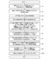
- FIG. 2 is a diagram showing a processing flow of local scanning executed by a processing unit 43 shown in FIG. 1;
- FIG. It is a figure which shows the structure of the position detection system 1 by the 2nd Embodiment of this invention.
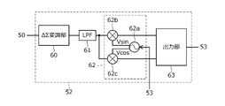
- 4 is a diagram showing an example of a specific internal configuration of a receiving section 52 shown in FIG. 3;
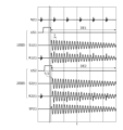
- FIG. 4A and 4B are diagrams for explaining a signal synthesis process performed by a processing unit 53 shown in FIG. 3;
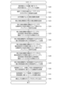
- FIG. 4 is a diagram showing a processing flow of local scanning executed by a processing unit 53 shown in FIG. 3;
- FIG. 1 is a diagram showing the configuration of a position detection system 1 according to the first embodiment of the present invention.
- the position detection system 1 includes a pen 2a compatible with the active electrostatic method and an electronic device 3 which is a position detection device for detecting the pen 2a.
- Examples of the electronic device 3 include a tablet computer and a device with a digitizer.
- the electronic device 3 includes a touch surface 3a which is a flat surface, a sensor 30a arranged directly below the touch surface 3a, a sensor controller 31a connected to the sensor 30a, a display 32 superimposed on the sensor 30a, It has a host processor 33 that controls each part of the electronic device 3 including these.
- the sensor 30a is a device having a structure in which a plurality of sensor electrodes, each of which is a uniform or mesh conductor, are arranged within the touch surface 3a.
- the plurality of sensor electrodes include a plurality of X electrodes each extending in the y direction parallel to the touch surface 3a and arranged at equal intervals in the x direction perpendicular to the y direction within the touch surface 3a, and and a plurality of Y electrodes arranged at regular intervals in the y direction.
- the sensor controller 31a is an integrated circuit having a function of deriving the position of the pen 2a within the touch surface 3a. Detection of the position of the pen 2a by the sensor controller 31a is performed by an active electrostatic method. Specifically, the sensor controller 31a is first configured to periodically transmit an uplink signal US.
- the uplink signal US in the active electrostatic system is a signal that notifies the pen 2a of the timing (reference timing) that serves as the reference for the operation, and has the role of transmitting a command that defines the operation of the pen 2a.
- the uplink signal US also serves as a transmission request signal for requesting the pen 2a to transmit a position signal (pen signal), which will be described later. Transmission of the uplink signal US is performed using some or all of the plurality of sensor electrodes that constitute the sensor 30a.
- the pen 2a has a pen tip electrode provided on the pen tip, and the uplink signal US is detected by detecting a change in the potential of the pen tip electrode.
- the pen 2a at the stage where the uplink signal US has not yet been detected performs the operation for detecting the uplink signal US continuously or intermittently.
- the pen 2a determines the transmission/reception schedule of the downlink signal DS and the next uplink signal US based on the detected uplink signal US, and transmits the downlink signal according to the determined transmission schedule. Performs transmission of DS and reception of the next uplink signal US.
- the downlink signal DS is obtained by modulating the carrier signal with a position signal, which is an unmodulated carrier signal, and predetermined data such as pen pressure values or data requested to be transmitted by a command in the uplink signal US. It is a signal including a data signal.
- the sensor controller 31a performs detection processing of this downlink signal DS in all the sensor electrodes forming the sensor 30a. Then, the position of the pen 2a is derived based on the received strength of the position signal at each sensor electrode (global scan).
- the pen 2a After the sensor controller 31a derives the position of the pen 2a once, the pen 2a sequentially transmits the position signal and the data signal as the downlink signal DS.
- the sensor controller 31a selects a predetermined number of sensor electrodes positioned near the position derived last time, and performs position signal detection processing on the selected sensor electrodes. Then, the position of the pen 2a is updated (local scan) based on the received strength of the position signal at each sensor electrode. Further, the sensor controller 31a selects one sensor electrode located near the previously derived position, and performs data signal detection processing on the selected sensor electrode. By demodulating the detected data signal, the data transmitted by the pen 2a is obtained.
- the sensor controller 31a is configured to sequentially supply the position derived as described above and the acquired data to the host processor 33.
- the host processor 33 is a central processing unit of the electronic device 3 and is configured to be able to execute various programs including drawing applications.
- the drawing application executes a process of generating digital ink based on the position and data supplied from the sensor controller 31a, and a process of storing the generated digital ink in the memory within the electronic device 3 and displaying it on the display 32 by the host processor. 33 is executed.
- the display 32 is a display device such as a liquid crystal display or an organic EL display.
- the sensor 30 a is arranged on the display surface of the display 32 so as to overlap the display 32 .
- a plurality of pixels are arranged in a matrix on the display surface of the display 32 , and the display 32 displays an image by controlling each pixel according to a display signal supplied from the host processor 33 .
- the control of each pixel in the display 32 is executed by sequentially performing the process of controlling the pixels row by row from one end to the other end in the row direction.
- the timing of changing rows is defined by horizontal sync pulses generated periodically within display 32 . Since this horizontal synchronizing pulse is a signal having a large amplitude, it is remarkably superimposed on the downlink signal DS detected by the sensor controller 31a as the above-described HSYNC noise.
- One of the purposes of the present invention is to avoid the deterioration of the SN ratio of the position signal due to this HSYNC noise. That is, since the position signal is used to derive the position of the pen 2a based on the reception strength of the position signal at each sensor electrode as described above, when the reception strength fluctuates due to HSYNC noise, the sensor controller 31a becomes difficult to correctly derive the position of the pen 2a. Therefore, when performing the local scan described above, the sensor controller 31a sets two detection periods in which the occurrence of the same HSYNC noise is expected, causes the pen 2a to transmit a position signal in each period, and receives a position signal in each period. By synthesizing these signals, the HSYNC noise is canceled while leaving the position signal. Details will be described later.
- global scanning does not require position detection with higher accuracy than local scanning, so it is not subject to the above processing in the present embodiment.
- the data signal contains an error detection code, even if an error occurs in the demodulation result due to HSYNC noise, it can be handled by detection and retransmission. Acquisition is required mainly when the pen tip of the pen 2a is in contact with the touch surface 3a (during pen-down), and it is expected that the reception strength of the data signal is sufficiently large compared to the HSYNC noise during pen-down. Therefore, in the present embodiment, the above processing is not performed. However, the global scan and data signals may be subject to the above processing.
- the sensor controller 31a includes a switching section 40, a transmitting section 41, a plurality of receiving sections 42, and a processing section 43.
- the switching unit 40 is a functional unit that switches the connection destination of each sensor electrode between the transmitting unit 41 and a plurality of receiving units 42 under the control of the processing unit 43 .
- the transmission unit 41 is a functional unit that supplies an uplink signal US to one or more sensor electrodes connected via the switching unit 40 under the control of the processing unit 43 .
- Each of the plurality of receiving units 42 is a functional unit that receives downlink signals DS arriving at sensor electrodes (receiving electrodes) connected via the switching unit 40 . Specifically, it is configured to periodically acquire the potential of the sensor electrode and output to the processing unit 43 a time-series signal composed of a series of potentials acquired as a result. This time-series signal becomes a signal in which HSYNC noise is superimposed on the downlink signal DS.
- the processing unit 43 is a functional unit that performs global scanning of the pen 2a, local scanning of the pen 2a, and reception of data from the pen 2a through control of the switching unit 40, the transmitting unit 41, and each receiving unit 42. Among these, in the processing of the local scan, the processing unit 43 sets two detection periods in which the generation of HSYNC noise having the same content is expected, and causes the pen 2a to transmit a position signal in each period. By synthesizing the supplied time-series signals, a process of canceling HSYNC noise while preserving the position signal is performed. This point will be described in detail below with reference to the processing flow of local scanning.
- FIG. 2 is a diagram showing a processing flow of local scanning executed by the processing unit 43.
- the processing unit 43 first selects a predetermined number of sensor electrodes based on the previously derived position of the pen 2a (step S1), and connects the receiving unit 42 to each of the selected predetermined number of sensor electrodes. Connect (step S2).
- the processing unit 43 is configured to select the same number of X electrodes and Y electrodes in descending order of the position of the pen 2a derived last time.
- the predetermined number is equal to or less than the total number of the receivers 42, and each sensor electrode selected in step S1 is connected to different receivers 42 from each other.
- a second detection period which is a period after the detection period ends, is set (step S4).
- the first detection period and the second detection period are periods each having a time length that is a natural number multiple of the HSYNC noise generation period, and are set to have the same time length.
- the processing unit 43 sets the first detection period and the second detection period so that the phases of the HSYNC noises substantially match each other.
- substantially matching means matching within the variation error range of the HSYNC noise generation period.
- the processing unit 43 transmits the position signal in synchronization with the first detection period, and transmits the position signal whose phase is inverted with respect to the position signal transmitted in synchronization with the first detection period.
- An uplink signal US requesting transmission in synchronization with the detection period 2 is transmitted (step S5).
- This uplink signal US includes data indicating the elapsed time from the above-described reference timing to the start timing of each of the first detection period and the second detection period. Based on this data, the pen 2a , during each of the first detection period and the second detection period.
- the processing unit 43 stores the time-series signal output from each receiving unit 42 during the first detection period as a first received signal (step S6), and stores each receiving unit within the second detection period. 42 is stored as a second received signal (step S7). Then, the position signal transmitted by the pen 2a is acquired based on the stored first received signal and second received signal for each receiving unit 42 (step S8).
- the position signal transmitted by the pen 2a in synchronization with the first detection period is S(t)
- the position signal transmitted by the pen 2a in synchronization with the second detection period is ⁇ S(t).
- the first detection period and the second detection period are set so that the phases of the HSYNC noise substantially match
- the HSYNC noise generated in the first detection period is N(t)
- the HSYNC noise occurring in the second detection period is also denoted as N(t).
- the first received signal is N(t)+S(t) and the second received signal is N(t)-S(t).
- step S8 the processing unit 43 subtracts the second received signal from the first received signal, that is, equivalent to the calculation of (N(t)+S(t))-(N(t)-S(t)). method to acquire the position signal transmitted by the pen 2a.
- a specific implementation method of this calculation is not particularly limited, and may be performed by, for example, a digital circuit or an analog circuit.
- the processing unit 43 can acquire only the position signal S(t).
- the processing unit 43 derives the position of the pen 2a based on the reception strength (amplitude) of the position signal acquired in step S8 for each receiving unit 42 (step S9). Specifically, the strength distribution of the position signal within the touch surface 3a is derived based on the received strength of the position signal at each sensor electrode, and the vertex of this distribution is obtained as the position of the pen 2a.
- the processing unit 43 that derived the position of the pen 2a outputs the derived position to the host processor (step S10), and ends the process.
- HSYNC noise can be canceled while leaving the position signal. Noise can be removed. Therefore, even when a high-resolution display is used as the display 32, it is possible to avoid a decrease in the SN ratio of the position signal, and as a result, it is possible to detect the position of the pen 2a with high accuracy. .
- FIG. 3 is a diagram showing the configuration of the position detection system 1 according to the second embodiment of the present invention.
- the position detection system 1 according to the present embodiment uses the pen 2b compatible with the electromagnetic induction method instead of the pen 2a compatible with the active electrostatic method, and the sensor 30b and the sensor controller 31b instead of the sensor 30a and the sensor controller 31a. is different from the position detection system 1 according to the first embodiment. Since other points are the same as the position detection system 1 according to the first embodiment, the following description focuses on the points of difference.
- the sensor 30b is a device having a structure in which a plurality of loop electrodes are arranged within the touch surface 3a.
- the plurality of loop electrodes each extend in the y direction parallel to the touch surface 3a, and the plurality of X electrodes arranged side by side in the x direction perpendicular to the y direction within the touch surface 3a, and the plurality of X electrodes each extending in the x direction. and a plurality of Y electrodes arranged side by side in the y direction.
- the sensor controller 31b is an integrated circuit having a function of detecting the position of the pen 2b within the touch surface 3a. Detection of the position of the pen 2b by the sensor controller 31b is performed by an electromagnetic induction method.
- the pen 2b is configured to have a resonance circuit including a coil and a capacitor.
- the sensor controller 31b supplies an uplink signal US, which is an AC signal having a frequency equal to the resonance frequency of the resonance circuit in the pen 2b, to one or more of the plurality of loop electrodes forming the sensor 30b over a certain period of time. do. Energy is then stored in the capacitor within the pen 2b due to mutual induction between the loop electrode and the coil within the pen 2b.
- the sensor controller 31b finishes supplying the uplink signal US, the power stored in the coil of the pen 2b appears in the loop electrodes due to mutual induction.
- the pen 2b uses this phenomenon to transmit the downlink signal DS.
- the downlink signal DS transmitted by the electromagnetic induction method is also composed of a position signal (pen signal), which is an unmodulated carrier wave signal, and predetermined data such as pen pressure value or an uplink signal US, as in the case of the active electrostatic method. and a data signal obtained by modulating a carrier signal with the data requested to be transmitted by the command within.
- pen signal position signal
- predetermined data such as pen pressure value or an uplink signal US
- a data signal obtained by modulating a carrier signal with the data requested to be transmitted by the command within At the stage when the sensor controller 31b has not yet derived the position of the pen 2b, the pen 2b transmits only the position signal as the downlink signal DS.
- the sensor controller 31b performs detection processing of this downlink signal DS in all the loop electrodes forming the sensor 30b. Then, the position of the pen 2b is derived based on the received strength of the position signal at each loop electrode (global scan).
- the pen 2b After the sensor controller 31b derives the position of the pen 2b once, the pen 2b sequentially transmits the position signal and the data signal as the downlink signal DS.
- the sensor controller 31b selects a predetermined number of loop electrodes positioned near the previously derived position, and performs position signal detection processing on the selected loop electrodes. Then, the position of the pen 2b is updated (local scan) based on the received strength of the position signal at each loop electrode. Further, the sensor controller 31b selects one loop electrode located near the previously derived position, and performs data signal detection processing on the selected loop electrode. By demodulating the detected data signal, the data transmitted by the pen 2b is acquired.
- the sensor controller 31b includes a switching unit 50, a transmitting unit 51, a plurality of receiving units 52, and a processing unit 53.
- the switching unit 50 is a functional unit that switches the connection destination of each loop electrode between the transmitting unit 51 and the plurality of receiving units 52 under the control of the processing unit 53 .
- the transmission unit 51 is a functional unit that supplies an uplink signal US to one or more loop electrodes connected via the switching unit 50 under the control of the processing unit 53 .
- Each of the plurality of receiving units 52 is a functional unit that receives downlink signals DS arriving at loop electrodes (receiving electrodes) connected via the switching unit 50 .
- Each receiving unit 52 has a detection circuit that extracts the frequency component of the carrier wave signal of the downlink signal DS from the change in potential difference appearing across the connected loop electrodes. 53.
- the detection circuit in each receiving section 52 can be configured by either an analog circuit or a digital circuit.
- the detector circuit if implemented digitally, is configured to perform a digital Fourier transform (DFT) using a series of digital values (basis vectors Vsin, Vcos, described below) indicative of the carrier signal of the downlink signal DS.
- DFT digital Fourier transform
- FIG. 4 is a diagram showing an example of a specific internal configuration of the receiving unit 52.
- the detection circuit is configured by a digital circuit.
- the receiving section 52 in this case includes a ⁇ modulation section 60 , a low-pass filter 61 , a detection circuit 62 and an output section 63 .
- the ⁇ modulation unit 60 performs ⁇ modulation on an analog signal indicated by a change in potential difference appearing across the loop electrodes connected via the switching unit 50, thereby generating a series of digital values each having a value of 0 or 1. This is the output circuit.
- the low-pass filter 61 is a decimation filter that counts (adds) the digital values output by the delta-sigma modulation unit 60 at regular time intervals to obtain an arithmetic mean and outputs the result.
- the output signal of the low-pass filter 61 is a digital signal obtained by restoring the analog signal input to the ⁇ modulation section 60 using a digital value.
- the detection circuit 62 is a circuit that performs frequency analysis of the output signal of the low-pass filter 61, and includes an oscillator 62a and mixers 62b and 62c.
- the oscillator 62 a is configured to output two types of basis vectors Vsin and Vcos under the control of the processing unit 53 .
- the basis vector Vsin is a vector representing the sine waveform of the carrier signal of the downlink signal DS, and is expressed as ⁇ 0, +1, 0, -1, 0, +1, 0, -1 ⁇ , for example.
- the basis vector Vcos is a vector representing the cosine waveform of the carrier signal of the downlink signal DS, and is expressed as ⁇ +1, 0, -1, 0, +1, 0, -1, 0 ⁇ , for example.
- the mixer 62b obtains the convolution sum (inner product) of the output signal of the low-pass filter 61 and the basis vector Vsin generated by the oscillator 62a, and supplies the result to the output section 63 as a quadrature component signal.
- the mixer 62c obtains the convolution sum (inner product) of the output signal of the low-pass filter 61 and the basis vector Vcos generated by the oscillator 62a, and supplies the result to the output section 63 as an in-phase component signal.
- the control of the oscillator 62a by the processing unit 53 is performed to change the phases of the basis vectors Vsin and Vcos supplied from the oscillator 62a to the mixers 62b and 62c during the first detection period and the second detection period.
- the phases of the basis vectors Vsin and Vcos in the second detection period are delayed by a half cycle of the carrier signal compared to the basis vectors Vsin and Vcos in the first detection period, thereby achieving the second detection period.
- the detection circuit 62 is caused to perform frequency analysis while the phases of the basis vectors Vsin and Vcos are inverted. This point will be described in more detail later with reference to FIG.
- the output unit 63 obtains a matching degree vector based on the in-phase component signal and the quadrature component signal supplied from the detection circuit 62, and uses a window of a predetermined time length to calculate the moving average of the length and slope of the matching degree vector. , and sequentially outputs the obtained average value of the length as the reception intensity and the obtained average value of the slope as the phase to the processing unit 53 shown in FIG.
- the output unit 63 performs demodulation processing for acquiring data transmitted by the pen 2 b based on the acquired reception intensity and phase, and also performs processing for outputting the data obtained as a result to the processing unit 53 .
- the processing unit 53 performs global scanning of the pen 2b, local scanning of the pen 2b, And, it is a functional unit that receives data from the pen 2b. Among these, in the processing of the local scan, the processing unit 53 sets two detection periods in which the generation of HSYNC noise with the same content is expected, and causes the pen 2b to transmit a position signal in each period. A process of canceling HSYNC noise while preserving the position signal is performed by combining the signals indicated by the series of received strengths provided.
- FIG. 5 is a diagram for explaining signal synthesizing processing executed by the processing unit 53.
- FIG. In the figure, the horizontal axis represents time and the vertical axis represents amplitude, and the figure shows simulated waveforms of signals related to this embodiment.
- the HSYNC noise N(t) the first position signal S1(t) transmitted from the pen 2b during the first detection period DE1
- the signal from the receiving unit 52 to the processing unit during the first detection period DE1 53 a second position signal S2(t) transmitted from the pen 2b within a second detection period DE2, a second detection
- a second received signal R2(t) indicated by a series of reception intensities supplied from the receiver 52 to the processor 53 within the period DE2, and a position signal SF(t) finally obtained by the processor 53.
- FIG. 5 shows a period during which the first uplink signal UP1 corresponding to the first detection period DE1 is transmitted, and a period during which the second uplink signal UP2 corresponding to the second detection period DE2 is transmitted. It also shows the period during which
- the first detection period DE1 and the second detection period DE2 are shown at the same position on the time axis. As described in the first embodiment, this is the period after the first detection period DE1 ends. Further, considering that the first detection period DE1 and the second detection period DE1 are set so that the phases of the respective HSYNC noises substantially match, in the simulation of FIG. The waveform of each signal was derived using the same HSYNC noise N(t) in the detection period DE1 and the second detection period DE2.
- the processing unit 53 that has set the first detection period DE1 and the second detection period DE2 first transmits the first uplink signal UP1 so that the transmission ends at the start timing of the first detection period DE1.
- transmission of the first position signal S1(t) from the pen 2b is started at the start timing of the first detection period DE1.
- the processing unit 53 performs detection at a timing delayed from the start timing of the second detection period DE2 by a period T/2, which is half the period T of the carrier wave signal of the downlink signal DS.
- a second uplink signal UP2 is transmitted to end the transmission.
- transmission of the second position signal S2(t) from the pen 2b is started at a timing delayed by the period T/2 from the start timing of the second detection period DE2.
- the processing unit 53 causes the oscillator 62a shown in FIG. 4 to start outputting the basis vectors Vsin and Vcos in synchronization with the start timing of the first detection period DE1.
- the first received signal R1(t) supplied from the receiver 52 to the processor 53 is the first position signal S1(t) on which the HSYNC noise N(t) is superimposed. ) is in phase.
- DS1(t) N(t)+S1(t).
- the processing unit 53 outputs the basis vectors Vsin and Vcos to the oscillator 62a shown in FIG. let it start.
- This measure is equivalent to delaying the phase of the basis vectors Vsin, Vcos in the second detection period by half the period of the carrier signal compared to the basis vectors Vsin, Vcos in the first detection period.
- the processing unit 53 After obtaining the first received signal R1(t) and the second received signal R2(t) as described above, the processing unit 53 combines them to generate the position signal SF(t). Specifically, as in the first embodiment, subtraction of the second received signal from the first received signal, that is, (N(t)+S1(t))-(N(t)-S2(t ))) to generate the position signal SF(t).
- a specific implementation method of this calculation is not particularly limited, and for example, it may be performed by a digital circuit or an analog circuit.
- SF(t) 2 ⁇ S1(t), so as shown in FIG. 5, the position signal SF(t) includes only the component of the position signal S1(t) transmitted by the pen 2b. will remain.
- FIG. 6 is a diagram showing a processing flow of local scanning executed by the processing unit 53.
- the processing unit 53 first selects a predetermined number of loop electrodes based on the previously derived position of the pen 2b (step S20), and connects the receiving unit 52 to each of the selected predetermined number of loop electrodes. Connect (step S21).
- the processing unit 53 is configured to select the same number of X-side antennas and Y-side antennas in order from the one closest to the previously derived position of the pen 2b.
- the predetermined number is equal to or less than the total number of the receiving sections 52, and the loop electrodes selected in step S1 are connected to different receiving sections 52 from each other.
- a second detection period which is a period after the detection period ends, is set (step S23). The relationship between the first detection period and the second detection period thus set is as described in the first embodiment.
- the processing unit 53 transmits an uplink signal US requesting to start transmitting the position signal at the start timing of the first detection period (step S24). Specifically, as described with reference to FIG. 5, the uplink signal US is transmitted so that the transmission ends at the start timing of the first detection period. Also, the processing unit 53 causes the oscillator 62a in the detection circuit 62 of each receiving unit 52 to start outputting the basis vectors Vsin and Vcos at the start timing of the first detection period (step S25). Then, a series of reception intensities output from the respective receivers 52 during the first detection period are stored as a first reception signal (step S26).
- the processing unit 53 transmits an uplink signal US requesting the start of transmission of the position signal at a timing delayed by a half cycle of the carrier wave signal from the start timing of the second detection period (step S27). Specifically, as described with reference to FIG. 5, the uplink signal US is transmitted so that the transmission ends at a timing delayed by half the cycle of the carrier wave signal from the start timing of the second detection period. Further, the processing unit 53 starts outputting the basis vectors Vsin and Vcos to the oscillator 62a in the detection circuit 62 of each receiving unit 52 at a timing delayed by half the cycle of the carrier wave signal from the start timing of the second detection period. (step S28). Then, a series of reception intensities output from the respective receivers 52 during the second detection period are stored as a second reception signal (step S29).
- the processing unit 53 that has acquired the first received signal and the second received signal from each receiving unit 52 as described above, based on the stored first received signal and second received signal for each receiving unit 52 Then, a process of acquiring a position signal is performed (step S30). Specifically, as described above, the position signal is obtained by subtracting the second received signal from the first received signal.
- the processing unit 53 derives the position of the pen 2b based on the reception strength (amplitude) of the position signal acquired in step S30 for each receiving unit 52 (step S31). Specifically, the intensity distribution of the position signal within the touch surface 3a is derived based on the reception intensity of the position signal at each loop electrode, and the vertex of this distribution is obtained as the position of the pen 2b.
- the processing unit 53 that derived the position of the pen 2b outputs the derived position to the host processor (step S32), and ends the process.
- the position detection system 1 can cancel the HSYNC noise while leaving the position signal. can be removed. Therefore, even when a high-resolution display is used as the display 32, it is possible to avoid a decrease in the SN ratio of the position signal, and as a result, it is possible to detect the position of the pen 2b with high accuracy. .
- the pen 2b is caused to start transmitting the position signal at a timing delayed by half the cycle of the carrier signal from the start timing of the second detection period, and in the second detection period
- the phase of the basis vector was delayed by half the period of the carrier signal compared to the basis vector in the first detection period.
- 2b may start transmitting the position signal and advance the phase of the basis vectors in the second detection period by half the period of the carrier signal compared to the basis vectors in the first detection period.
- the second detection period is the period after the first detection period ends, but the first detection period is the period after the second detection period ends. It can be a certain thing.
- the sensor controllers 31a and 31b may also be configured to detect the position of a passive pointer such as a finger.
- the sensor 30a can also be used to detect the position of the passive pointer.
- the position of the passive pointer may be detected by arranging a sensor corresponding to the capacitance method so as to overlap the sensor 30b.
Landscapes
- Engineering & Computer Science (AREA)
- General Engineering & Computer Science (AREA)
- Theoretical Computer Science (AREA)
- Human Computer Interaction (AREA)
- Physics & Mathematics (AREA)
- General Physics & Mathematics (AREA)
- Position Input By Displaying (AREA)
Abstract
【課題】高解像度のディスプレイを用いる場合にも、ペン信号のSN比の低下を回避できるようにする。 【解決手段】本発明によるペン信号の検出方法は、ペンから送出される交流信号であるペン信号の検出方法であって、ノイズの発生周期に基づき、第1の検出期間、及び、前記第1の検出期間が終了した後の期間である第2の検出期間を設定するステップS4と、第1の検出期間に同期してペン信号を送信し、かつ、第1の検出期間に同期して送信するペン信号に対して位相が反転した状態のペン信号を第2の検出期間に同期して送信するよう要求するアップリンク信号をペンに対して送信するステップS5と、第1の検出期間にペンから受信される第1の受信信号、及び、第2の検出期間にペンから受信される第2の受信信号に基づいてペン信号を取得するステップS8と、を含む。
Description
本発明はペン信号の検出方法、センサコントローラ、及び位置検出システムに関し、特に、周期的なノイズが発生する環境下でのペン信号の検出方法と、そのようなペン信号の検出を行うセンサコントローラ及び位置検出システムに関する。
ディスプレイとタッチセンサとが重畳配置されるタイプのタッチ検出装置においては、ディスプレイの内部信号である水平同期(HSYNC)パルスに由来するノイズの発生が知られている。以下、このノイズを「HSYNCノイズ」と称する。
特許文献1には、HSYNCノイズが発生するタッチ検出装置の例が開示されている。同文献に記載のタッチ検出装置においては、水平同期パルスに同期したパルスを発生させ、このパルスに同期したタイミングで受信回路の入力を遮断しているので、位置検出に対するHSYNCノイズの影響を低減することが可能になる。
しかしながら、近年ディスプレイの高解像度化が進んでおり、水平同期パルスの周期が極めて短くなっている。一例では、例えば4K対応のディスプレイでは、1秒間に約2000回もの周期で水平同期パルスが発生する。そうすると、特許文献1のように水平同期パルスに同期したタイミングで受信回路の入力を遮断していては、受信回路によってペン信号を検出できる期間が極めて短くなってしまう。結果として、HSYNCノイズが受信回路に入力されないにもかかわらず、ペン信号の信号対ノイズ比(以下「SN比」という)が低下してしまうことになる。
したがって、本発明の目的の一つは、高解像度のディスプレイを用いる場合にもペン信号のSN比の低下を回避できるペン信号の検出方法、センサコントローラ、及び位置検出システムを提供することにある。
本発明によるペン信号の検出方法は、ペンから送出される交流信号であるペン信号の検出方法であって、ノイズの発生周期に基づき、第1の検出期間、及び、前記第1の検出期間が終了した後の期間である第2の検出期間を設定するステップと、前記第1の検出期間に同期して前記ペン信号を送信し、かつ、前記第1の検出期間に同期して送信する前記ペン信号に対して位相が反転した状態の前記ペン信号を前記第2の検出期間に同期して送信するよう要求する送信要求信号を前記ペンに対して送信するステップと、前記第1の検出期間に前記ペンから受信される第1の受信信号、及び、前記第2の検出期間に前記ペンから受信される第2の受信信号に基づいてペン信号を取得する取得ステップと、を含むペン信号の検出方法である。
本発明によるセンサコントローラは、ペンから送出される交流信号であるペン信号を検出するセンサコントローラであって、センサに対して送信要求信号を供給する送信部と、前記センサに到来した信号を受信する受信部と、前記送信部及び前記受信部を制御する処理部と、を有し、前記処理部は、ノイズの発生周期に基づき、第1の検出期間、及び、前記第1の検出期間が終了した後の期間である第2の検出期間を設定し、前記第1の検出期間に同期して前記ペン信号を送信し、かつ、前記第1の検出期間に同期して送信する前記ペン信号に対して位相が反転した状態の前記ペン信号を前記第2の検出期間に同期して送信するよう要求する送信要求信号を、前記送信部を介して前記ペンに対して送信し、前記第1の検出期間に前記受信部から出力される第1の受信信号、及び、前記第2の検出期間に前記受信部から出力される第2の受信信号に基づいてペン信号を取得する、センサコントローラである。
本発明による位置検出システムは、ペンと、前記ペンから送出される交流信号であるペン信号を検出するセンサコントローラと、を含む位置検出システムであって、前記センサコントローラは、センサに対して送信要求信号を供給する送信部と、前記センサに到来した信号を受信する受信部と、前記送信部及び前記受信部を制御する処理部と、を有し、前記処理部は、ノイズの発生周期に基づき、第1の検出期間、及び、前記第1の検出期間が終了した後の期間である第2の検出期間を設定し、前記第1の検出期間に同期して前記ペン信号を送信し、かつ、前記第1の検出期間に同期して送信する前記ペン信号に対して位相が反転した状態の前記ペン信号を前記第2の検出期間に同期して送信するよう要求する送信要求信号を、前記送信部を介して前記ペンに対して送信し、前記第1の検出期間に前記受信部から出力される第1の受信信号、及び、前記第2の検出期間に前記受信部から出力される第2の受信信号に基づいてペン信号を取得する、位置検出システムである。
本発明によれば、ペン信号を残しつつノイズを相殺することができるので、受信回路の入力を遮断することなく、ペン信号からノイズを除去することができる。したがって、高解像度のディスプレイを用いる場合にも、ペン信号のSN比の低下を回避することが可能になる。
以下、添付図面を参照しながら、本発明の好ましい実施の形態について詳細に説明する。
図1は、本発明の第1の実施の形態による位置検出システム1の構成を示す図である。同図に示すように、位置検出システム1は、アクティブ静電方式に対応するペン2aと、ペン2aを検出する位置検出装置である電子機器3とを備えて構成される。電子機器3の例としては、タブレットコンピュータや、デジタイザを備えたデバイスが挙げられる。
電子機器3は、平坦な表面であるタッチ面3aと、タッチ面3aの直下に配置されたセンサ30aと、センサ30aに接続されたセンサコントローラ31aと、センサ30aと重畳配置されたディスプレイ32と、これらを含む電子機器3の各部を制御するホストプロセッサ33とを有している。
センサ30aは、それぞれ一様な又はメッシュ状の導体である各複数のセンサ電極がタッチ面3a内に配置された構造を有する装置である。複数のセンサ電極は、それぞれタッチ面3aに平行なy方向に延在し、かつ、タッチ面3a内でy方向に直交するx方向に等間隔に配置される複数のX電極と、それぞれx方向に延在し、かつ、y方向に等間隔に配置される複数のY電極とを含んで構成される。
センサコントローラ31aは、タッチ面3a内におけるペン2aの位置を導出する機能を有する集積回路である。センサコントローラ31aによるペン2aの位置の検出は、アクティブ静電方式によって実行される。具体的に説明すると、センサコントローラ31aはまず、アップリンク信号USを周期的に送信するよう構成される。アクティブ静電方式におけるアップリンク信号USは、ペン2aに動作の基準となるタイミング(基準タイミング)を通知するとともに、ペン2aの動作を規定するコマンドを送信する役割を有する信号である。アップリンク信号USはまた、後述する位置信号(ペン信号)の送信をペン2aに要求する送信要求信号としての役割も有している。アップリンク信号USの送信は、センサ30aを構成する各複数のセンサ電極の一部又は全部を用いて実行される。
ペン2aはペン先に設けられたペン先電極を有しており、このペン先電極の電位の変化を検出することにより、アップリンク信号USの検出を行う。未だアップリンク信号USを検出していない段階でのペン2aは、アップリンク信号USを検出するための動作を連続的又は断続的に行う。一旦アップリンク信号USを検出した後には、ペン2aは、検出したアップリンク信号USに基づいてダウンリンク信号DS及び次のアップリンク信号USの送受信スケジュールを決定し、決定した送信スケジュールに従ってダウンリンク信号DSの送信及び次のアップリンク信号USの受信を実行する。
ダウンリンク信号DSは、無変調の搬送波信号である位置信号と、筆圧値等の所定のデータ又はアップリンク信号US内のコマンドにより送信を要求されたデータによって搬送波信号を変調することによって得られるデータ信号とを含む信号である。センサコントローラ31aが未だペン2aの位置を導出していない段階では、ペン2aは、ダウンリンク信号DSとして位置信号のみを送信する。センサコントローラ31aは、センサ30aを構成するすべてのセンサ電極においてこのダウンリンク信号DSの検出処理を行う。そして、各センサ電極における位置信号の受信強度に基づいて、ペン2aの位置を導出する(グローバルスキャン)。こうしてセンサコントローラ31aが一度ペン2aの位置を導出した後には、ペン2aは、ダウンリンク信号DSとして位置信号及びデータ信号を順次送信する。センサコントローラ31aは、前回導出した位置の近傍に位置する所定本数のセンサ電極を選択し、選択したセンサ電極において位置信号の検出処理を行う。そして、各センサ電極における位置信号の受信強度に基づいて、ペン2aの位置を更新する(ローカルスキャン)。また、センサコントローラ31aは、前回導出した位置の近傍に位置する1本のセンサ電極を選択し、選択したセンサ電極においてデータ信号の検出処理を行う。そして、検出したデータ信号を復調することにより、ペン2aが送信したデータを取得する。
センサコントローラ31aは、以上のようにして導出した位置、及び、取得したデータを、逐次ホストプロセッサ33に供給するよう構成される。ホストプロセッサ33は電子機器3の中央処理装置であり、描画アプリケーションを含む各種のプログラムを実行可能に構成される。描画アプリケーションは、センサコントローラ31aから供給された位置及びデータに基づいてデジタルインクを生成する処理、並びに、生成したデジタルインクを電子機器3内のメモリに記憶するとともにディスプレイ32に表示する処理をホストプロセッサ33に実行させるプログラムである。
ディスプレイ32は、液晶ディスプレイ又は有機ELディスプレイなどの表示装置である。センサ30aは、ディスプレイ32の表示面上に、ディスプレイ32と重ねて配置される。ディスプレイ32の表示面内には複数の画素がマトリクス状に配置されており、ディスプレイ32は、ホストプロセッサ33から供給される表示信号に従って各画素を制御することによって、映像の表示を行う。
ディスプレイ32における各画素の制御は、行方向の一方端から他方端に向かって順に画素を制御する処理を1行ずつ順に行うことによって実行される。行を変更するタイミングは、ディスプレイ32内で周期的に生成される水平同期パルスによって規定される。この水平同期パルスは大きな振幅を有する信号であることから、上述したHSYNCノイズとして、センサコントローラ31aが検出するダウンリンク信号DSに顕著に重畳することになる。
本発明の目的の1つは、このHSYNCノイズによる位置信号のSN比の低下を回避することにある。すなわち、位置信号は、上述したように各センサ電極における位置信号の受信強度に基づいてペン2aの位置を導出するために用いられるものであることから、HSYNCノイズによって受信強度が変動すると、センサコントローラ31aは、正しくペン2aの位置を導出することが困難になる。そこでセンサコントローラ31aは、上述したローカルスキャンを実行する際に、同じ内容のHSYNCノイズの発生が期待される2つの検出期間を設定し、それぞれにおいてペン2aに位置信号を送信させ、それぞれにおいて受信された信号を合成することによって、位置信号を残しつつHSYNCノイズを相殺する処理を行う。詳細については、後述する。
なお、グローバルスキャンは、ローカルスキャンに比べて高い精度での位置検出が必要とされないことから、本実施の形態では上記処理の対象としない。また、データ信号についても、データ信号内には誤り検出符号が含まれていることから、もしHSYNCノイズによって復調結果に誤りが生じたとしても検出及び再送によって対応可能であり、しかも、データ信号の取得が必要になるのは主にペン2aのペン先がタッチ面3aに接触しているとき(ペンダウン時)であり、ペンダウン時にはHSYNCノイズに比べてデータ信号の受信強度が十分に大きいと期待されることから、本実施の形態では上記処理の対象としない。ただし、グローバルスキャン及びデータ信号を上記処理の対象としても構わない。
図1に示すように、センサコントローラ31aは、切替部40と、送信部41と、複数の受信部42と、処理部43とを有して構成される。切替部40は、処理部43による制御に従い、各センサ電極の接続先を送信部41と複数の受信部42との間で切り替える機能部である。送信部41は、処理部43による制御に従い、切替部40を介して接続された1以上のセンサ電極に対してアップリンク信号USを供給する機能部である。
複数の受信部42はそれぞれ、切替部40を介して接続されたセンサ電極(受信電極)に到来したダウンリンク信号DSを受信する機能部である。具体的には、センサ電極の電位を周期的に取得し、その結果として取得される一連の電位によって構成される時系列信号を処理部43に出力するよう構成される。この時系列信号は、ダウンリンク信号DSにHSYNCノイズが重畳された信号となる。
処理部43は、切替部40、送信部41、及び各受信部42の制御を通じて、ペン2aのグローバルスキャン、ペン2aのローカルスキャン、及び、ペン2aからのデータの受信を行う機能部である。このうちローカルスキャンの処理の中において処理部43は、同じ内容のHSYNCノイズの発生が期待される2つの検出期間を設定し、それぞれにおいてペン2aに位置信号を送信させ、それぞれにおいて受信部42から供給される時系列信号を合成することによって、位置信号を残しつつHSYNCノイズを相殺する処理を実行する。以下、この点について、ローカルスキャンの処理フローを参照しながら詳しく説明する。
図2は、処理部43が実行するローカルスキャンの処理フローを示す図である。同図に示すように、処理部43はまず、前回導出したペン2aの位置に基づいて所定本数のセンサ電極を選択し(ステップS1)、選択した所定本数のセンサ電極のそれぞれに受信部42を接続する(ステップS2)。ステップS1において処理部43は、前回導出したペン2aの位置に近いものから順に、X電極及びY電極を同数ずつ選択するよう構成される。また、上記所定本数は受信部42の総数以下の数であり、ステップS1において選択された各センサ電極は、互いに異なる受信部42に接続される。
次に処理部43は、ホストプロセッサ33から水平同期パルスの発生周期(=HSYNCノイズの発生周期)を取得し(ステップS3)、取得した周期に基づいて、第1の検出期間と、第1の検出期間が終了した後の期間である第2の検出期間とを設定する(ステップS4)。第1の検出期間及び第2の検出期間はそれぞれ、HSYNCノイズの発生周期の自然数倍の時間長を有する期間であり、互いに同じ時間長に設定される。また、処理部43は、それぞれにおけるHSYNCノイズの位相が略一致するように、第1の検出期間及び第2の検出期間の設定を行う。ここで「略一致」とは、HSYNCノイズの発生周期の変動誤差の範囲での一致をいう。
続いて処理部43は、第1の検出期間に同期して位置信号を送信し、かつ、第1の検出期間に同期して送信する位置信号に対して位相が反転した状態の位置信号を第2の検出期間に同期して送信するよう要求するアップリンク信号USを送信する(ステップS5)。このアップリンク信号USには、上述した基準タイミングから第1の検出期間及び第2の検出期間それぞれの開始タイミングまでの経過時間を示すデータが含まれており、ペン2aは、このデータに基づいて、第1の検出期間及び第2の検出期間それぞれの中で位置信号を送信する。
次に処理部43は、第1の検出期間内に各受信部42から出力される時系列信号を第1の受信信号として記憶する(ステップS6)とともに、第2の検出期間内に各受信部42から出力される時系列信号を第2の受信信号として記憶する(ステップS7)。そして、受信部42ごとに、記憶した第1の受信信号及び第2の受信信号に基づいて、ペン2aが送信した位置信号を取得する(ステップS8)。
ここで、ペン2aが第1の検出期間に同期して送信する位置信号をS(t)とすると、ペン2aが第2の検出期間に同期して送信する位置信号は-S(t)と表される。また、HSYNCノイズの位相が略一致するように第1の検出期間及び第2の検出期間の設定を行っていることから、第1の検出期間内に発生するHSYNCノイズをN(t)とすると、第2の検出期間内に発生するHSYNCノイズもN(t)と表される。そして、これらの表記を用いると、第1の受信信号はN(t)+S(t)となり、第2の受信信号はN(t)-S(t)となる。
ステップS8において処理部43は、第1の受信信号から第2の受信信号の減算、すなわち、(N(t)+S(t))-(N(t)-S(t))の演算と等価な方法により、ペン2aが送信した位置信号を取得する。この演算の具体的な実現方法は特に限定されず、例えばデジタル回路によって行ってもよいし、アナログ回路によって行ってもよい。演算の結果としてHSYNCノイズN(t)が相殺され、位置信号S(t)のみが残るので、処理部43は位置信号S(t)のみを取得できることになる。
次に処理部43は、各受信部42についてステップS8で取得した位置信号の受信強度(振幅)に基づき、ペン2aの位置を導出する(ステップS9)。具体的には、各センサ電極における位置信号の受信強度に基づいてタッチ面3a内における位置信号の強度分布を導出し、この分布の頂点をペン2aの位置として取得する。ペン2aの位置を導出した処理部43は、導出した位置をホストプロセッサに出力し(ステップS10)、処理を終了する。
以上説明したように、本実施の形態による位置検出システム1によれば、位置信号を残しつつHSYNCノイズを相殺することができるので、受信部42の入力を遮断することなく、受信した信号からHSYNCノイズを除去することができる。したがって、ディスプレイ32として高解像度のディスプレイを用いる場合にも、位置信号のSN比の低下を回避することが可能になり、その結果として、ペン2aの位置を高い精度で検出することが可能になる。
図3は、本発明の第2の実施の形態による位置検出システム1の構成を示す図である。本実施の形態による位置検出システム1は、アクティブ静電方式に対応するペン2aに代えて電磁誘導方式に対応するペン2bを用いる点、センサ30a及びセンサコントローラ31aに代えてセンサ30b及びセンサコントローラ31bを用いる点で、第1の実施の形態による位置検出システム1と相違する。その他の点では第1の実施の形態による位置検出システム1と同様であるので、以下では相違点に着目して説明する。
センサ30bは、複数のループ電極がタッチ面3a内に配置された構造を有する装置である。複数のループ電極は、それぞれタッチ面3aに平行なy方向に延在し、かつ、タッチ面3a内でy方向に直交するx方向に並置される複数のX電極と、それぞれx方向に延在し、かつ、y方向に並置される複数のY電極とを含んで構成される。
センサコントローラ31bは、タッチ面3a内におけるペン2bの位置を検出する機能を有する集積回路である。センサコントローラ31bによるペン2bの位置の検出は、電磁誘導方式によって実行される。具体的に説明すると、まずペン2bは、コイル及びコンデンサを含む共振回路を有して構成される。センサコントローラ31bは、センサ30bを構成する複数のループ電極のうちの1つ以上に対し、一定期間にわたり、ペン2b内の共振回路の共振周波数に等しい周波数の交流信号であるアップリンク信号USを供給する。すると、ループ電極と、ペン2b内のコイルとの間の相互誘導により、ペン2b内のコンデンサにエネルギーが蓄積される。センサコントローラ31bがアップリンク信号USの供給を終了すると、ペン2bのコイルに蓄積された電力が相互誘導によってループ電極に現れる。ペン2bは、この現象を利用してダウンリンク信号DSの送信を行う。
電磁誘導方式によって送信されるダウンリンク信号DSも、アクティブ静電方式の場合と同様、無変調の搬送波信号である位置信号(ペン信号)と、筆圧値等の所定のデータ又はアップリンク信号US内のコマンドにより送信を要求されたデータによって搬送波信号を変調することによって得られるデータ信号とを含む信号となる。センサコントローラ31bが未だペン2bの位置を導出していない段階では、ペン2bは、ダウンリンク信号DSとして位置信号のみを送信する。センサコントローラ31bは、センサ30bを構成するすべてのループ電極において、このダウンリンク信号DSの検出処理を行う。そして、各ループ電極における位置信号の受信強度に基づいて、ペン2bの位置を導出する(グローバルスキャン)。こうしてセンサコントローラ31bが一度ペン2bの位置を導出した後には、ペン2bは、ダウンリンク信号DSとして位置信号及びデータ信号を順次送信する。センサコントローラ31bは、前回導出した位置の近傍に位置する所定本数のループ電極を選択し、選択したループ電極において位置信号の検出処理を行う。そして、各ループ電極における位置信号の受信強度に基づいて、ペン2bの位置を更新する(ローカルスキャン)。また、センサコントローラ31bは、前回導出した位置の近傍に位置する1本のループ電極を選択し、選択したループ電極においてデータ信号の検出処理を行う。そして、検出したデータ信号を復調することにより、ペン2bが送信したデータを取得する。
図3に示すように、センサコントローラ31bは、切替部50と、送信部51と、複数の受信部52と、処理部53とを有して構成される。切替部50は、処理部53による制御に従い、各ループ電極の接続先を送信部51と複数の受信部52との間で切り替える機能部である。送信部51は、処理部53による制御に従い、切替部50を介して接続された1以上のループ電極に対してアップリンク信号USを供給する機能部である。
複数の受信部52はそれぞれ、切替部50を介して接続されたループ電極(受信電極)に到来したダウンリンク信号DSを受信する機能部である。各受信部52は、接続されたループ電極の両端に現れる電位差の変化からダウンリンク信号DSの搬送波信号の周波数成分を取り出す検波回路を有しており、この検波回路により検出された信号を処理部53に出力するよう構成される。
各受信部52内の検波回路は、アナログ回路及びデジタル回路のいずれによっても構成され得る。デジタル回路により構成する場合の検波回路は、ダウンリンク信号DSの搬送波信号を示す一連のデジタル値(後述する基底ベクトルVsin,Vcos)を用いて、デジタルフーリエ変換(DFT)を行うよう構成される。
図4は、受信部52の具体的な内部構成の例を示す図である。同図には、検波回路をデジタル回路によって構成する場合の例を示している。同図に示すように、この場合の受信部52は、ΔΣ変調部60と、ローパスフィルタ61と、検波回路62と、出力部63とを有して構成される。ΔΣ変調部60は、切替部50を介して接続されたループ電極の両端に現れる電位差の変化により示されるアナログ信号のΔΣ変調を行うことにより、それぞれ0又は1の値を有する一連のデジタル値を出力する回路である。ローパスフィルタ61は、ΔΣ変調部60が出力したデジタル値を一定時間ごとにカウント(加算)することにより加算平均を取得し、出力するデシメーションフィルタである。ローパスフィルタ61の出力信号は、ΔΣ変調部60に入力されるアナログ信号をデジタル値によって復元したデジタル信号となる。
検波回路62は、ローパスフィルタ61の出力信号の周波数解析を行う回路であり、発振器62a及び混合器62b,62cを有して構成される。発振器62aは、処理部53の制御に応じて、2種類の基底ベクトルVsin,Vcosを出力するよう構成される。基底ベクトルVsinはダウンリンク信号DSの搬送波信号のサイン波形を示すベクトルであり、例えば{0,+1,0,-1,0,+1,0,-1}と表される。基底ベクトルVcosはダウンリンク信号DSの搬送波信号のコサイン波形を示すベクトルであり、例えば{+1,0,-1,0,+1,0,-1,0}と表される。混合器62bは、ローパスフィルタ61の出力信号と、発振器62aによって生成された基底ベクトルVsinとの畳み込み和(内積)を求め、その結果を直交成分信号として出力部63に供給する。混合器62cは、ローパスフィルタ61の出力信号と、発振器62aによって生成された基底ベクトルVcosとの畳み込み和(内積)を求め、その結果を同相成分信号として出力部63に供給する。
処理部53による発振器62aの制御は、上述した第1の検出期間と第2の検出期間とで、発振器62aから混合器62b,62cに供給する基底ベクトルVsin,Vcosの位相を変化させるために行われる。具体的には、第2の検出期間における基底ベクトルVsin,Vcosの位相を、第1の検出期間における基底ベクトルVsin,Vcosに比べて搬送波信号の半周期分だけ遅らせることにより、第2の検出期間において、基底ベクトルVsin,Vcosの位相を反転させた状態で検波回路62に周波数解析を実行させる。この点については、後ほど図5を参照しながら、より詳しく説明する。
出力部63は、検波回路62から供給される同相成分信号及び直交成分信号に基づいてマッチ度ベクトルを求め、さらに、所定時間長のウインドウを用いてマッチ度ベクトルの長さ及び傾きそれぞれの移動平均を求め、得られた長さの平均値を受信強度として、傾きの平均値を位相として、それぞれ図3に示した処理部53に逐次出力する機能部である。出力部63は、取得した受信強度及び位相に基づいてペン2bが送信したデータを取得する復調処理を行い、その結果として得られたデータを処理部53に出力する処理も行う。
図3に戻る。処理部53は、第1の実施の形態にて説明した処理部43と同様、切替部50、送信部51、及び各受信部52の制御を通じて、ペン2bのグローバルスキャン、ペン2bのローカルスキャン、及び、ペン2bからのデータの受信を行う機能部である。このうちローカルスキャンの処理の中において処理部53は、同じ内容のHSYNCノイズの発生が期待される2つの検出期間を設定し、それぞれにおいてペン2bに位置信号を送信させ、それぞれにおいて受信部52から供給される一連の受信強度によって示される信号を合成することによって、位置信号を残しつつHSYNCノイズを相殺する処理を実行する。
図5は、処理部53によって実行される信号の合成処理を説明する図である。同図の横軸は時間、縦軸は振幅であり、同図には本実施の形態に関連する各信号のシミュレーション波形を示している。具体的には、HSYNCノイズN(t)、第1の検出期間DE1内にペン2bから送信される第1の位置信号S1(t)、第1の検出期間DE1内に受信部52から処理部53に供給される一連の受信強度によって示される第1の受信信号R1(t)、第2の検出期間DE2内にペン2bから送信される第2の位置信号S2(t)、第2の検出期間DE2内に受信部52から処理部53に供給される一連の受信強度によって示される第2の受信信号R2(t)、及び、処理部53によって最終的に取得される位置信号SF(t)の波形を示している。また、図5には、第1の検出期間DE1に対応する第1のアップリンク信号UP1が送信されている期間、及び、第2の検出期間DE2に対応する第2のアップリンク信号UP2が送信されている期間についても図示している。
なお、図5においては、比較の便のため第1の検出期間DE1と第2の検出期間DE2とを時間軸上の同じ位置に示しているが、実際の第2の検出期間DE2は、第1の実施の形態で説明したとおり、第1の検出期間DE1が終了した後の期間である。また、それぞれのHSYNCノイズの位相が略一致するように第1の検出期間DE1と第2の検出期間DE1の設定が行われることに鑑み、同図のシミュレーションにおいては、便宜的に、第1の検出期間DE1と第2の検出期間DE2とで同じHSYNCノイズN(t)を用いて各信号の波形を導出した。
第1の検出期間DE1及び第2の検出期間DE2を設定した処理部53は、まず第1の検出期間DE1の開始タイミングで送信が終了するよう、第1のアップリンク信号UP1の送信を行う。これにより、図5に示すように、ペン2bからの第1の位置信号S1(t)の送信が第1の検出期間DE1の開始タイミングで開始される。また、処理部53は、第1の検出期間DE1が終了した後、ダウンリンク信号DSの搬送波信号の周期Tの半分の期間T/2だけ第2の検出期間DE2の開始タイミングから遅れたタイミングで送信が終了するよう、第2のアップリンク信号UP2の送信を行う。これにより、図5に示すように、ペン2bからの第2の位置信号S2(t)の送信が、第2の検出期間DE2の開始タイミングから期間T/2だけ遅れたタイミングで開始される。
第1の検出期間DE1において処理部53は、第1の検出期間DE1の開始タイミングに合わせて、図4に示した発振器62aに基底ベクトルVsin,Vcosの出力を開始させる。これにより、図5に示すように、受信部52から処理部53に供給される第1の受信信号R1(t)は、HSYNCノイズN(t)が重畳された第1の位置信号S1(t)と同位相の信号となる。数式で表すと、DS1(t)=N(t)+S1(t)となる。
また、第2の検出期間DE2において処理部53は、第2の検出期間DE2の開始タイミングから期間T/2だけ遅れたタイミングで、図4に示した発振器62aに基底ベクトルVsin,Vcosの出力を開始させる。この措置は、第2の検出期間における基底ベクトルVsin,Vcosの位相を、第1の検出期間における基底ベクトルVsin,Vcosに比べて搬送波信号の半周期分だけ遅らせていることと等価である。これにより、図5に示すように、受信部52から処理部53に供給される第2の受信信号R2(t)は、第1の受信信号R1(t)に比べて極性が反転した信号となる。数式で表すと、DS2(t)=N(t)+S2(t)=N(t)-S1(t)となる。
以上のようにして第1の受信信号R1(t)及び第2の受信信号R2(t)を得た処理部53は、これらを合成することによって、位置信号SF(t)を生成する。具体的には、第1の実施の形態と同様、第1の受信信号から第2の受信信号の減算、すなわち、(N(t)+S1(t))-(N(t)-S2(t))の演算と等価な方法により、位置信号SF(t)の生成を行う。この演算の具体的な実現方法も特に限定されず、例えばデジタル回路によって行ってもよいし、アナログ回路によって行ってもよい。演算の結果としてSF(t)=2×S1(t)となるので、図5にも示すように、位置信号SF(t)には、ペン2bが送信した位置信号S1(t)の成分のみが残ることになる。
図6は、処理部53が実行するローカルスキャンの処理フローを示す図である。同図に示すように、処理部53はまず、前回導出したペン2bの位置に基づいて所定本数のループ電極を選択し(ステップS20)、選択した所定本数のループ電極のそれぞれに受信部52を接続する(ステップS21)。ステップS20において処理部53は、前回導出したペン2bの位置に近いものから順に、X側アンテナ及びY側アンテナを同数ずつ選択するよう構成される。また、上記所定本数は受信部52の総数以下の数であり、ステップS1において選択された各ループ電極は、互いに異なる受信部52に接続される。
次に処理部53は、ホストプロセッサ33より水平同期パルスの発生周期(=HSYNCノイズの発生周期)を取得し(ステップS22)、取得した周期に基づいて、第1の検出期間と、第1の検出期間が終了した後の期間である第2の検出期間とを設定する(ステップS23)。こうして設定される第1の検出期間及び第2の検出期間の関係は、第1の実施の形態で説明したとおりである。
続いて処理部53は、第1の検出期間の開始タイミングで位置信号の送信を開始するよう要求するアップリンク信号USを送信する(ステップS24)。具体的には、図5を参照して説明したように、第1の検出期間の開始タイミングで送信が終了するようアップリンク信号USの送信を行う。また、処理部53は、第1の検出期間の開始タイミングで、各受信部52の検波回路62内の発振器62aに基底ベクトルVsin,Vcosの出力を開始させる(ステップS25)。そして、第1の検出期間内に各受信部52から出力される一連の受信強度を第1の受信信号として記憶する(ステップS26)。
次に処理部53は、第2の検出期間の開始タイミングから搬送波信号の半周期分遅れたタイミングで位置信号の送信を開始するよう要求するアップリンク信号USを送信する(ステップS27)。具体的には、図5を参照して説明したように、第2の検出期間の開始タイミングから搬送波信号の半周期分だけ遅れたタイミングで送信が終了するようアップリンク信号USの送信を行う。また、処理部53は、第2の検出期間の開始タイミングから搬送波信号の半周期分だけ遅れたタイミングで、各受信部52の検波回路62内の発振器62aに基底ベクトルVsin,Vcosの出力を開始させる(ステップS28)。そして、第2の検出期間内に各受信部52から出力される一連の受信強度を第2の受信信号として記憶する(ステップS29)。
以上のようにして各受信部52から第1の受信信号及び第2の受信信号を取得した処理部53は、受信部52ごとに、記憶した第1の受信信号及び第2の受信信号に基づいて、位置信号を取得する処理を行う(ステップS30)。具体的には、上述したように、第1の受信信号から第2の受信信号を減算することによって、位置信号を取得する。
次に処理部53は、各受信部52についてステップS30で取得した位置信号の受信強度(振幅)に基づき、ペン2bの位置を導出する(ステップS31)。具体的には、各ループ電極における位置信号の受信強度に基づいてタッチ面3a内における位置信号の強度分布を導出し、この分布の頂点をペン2bの位置として取得する。ペン2bの位置を導出した処理部53は、導出した位置をホストプロセッサに出力し(ステップS32)、処理を終了する。
以上説明したように、本実施の形態による位置検出システム1によっても、位置信号を残しつつHSYNCノイズを相殺することができるので、受信部52の入力を遮断することなく、受信した信号からHSYNCノイズを除去することができる。したがって、ディスプレイ32として高解像度のディスプレイを用いる場合にも、位置信号のSN比の低下を回避することが可能になり、その結果として、ペン2bの位置を高い精度で検出することが可能になる。
以上、本発明の好ましい実施の形態について説明したが、本発明はこうした実施の形態に何等限定されるものではなく、本発明が、その要旨を逸脱しない範囲において、種々なる態様で実施され得ることは勿論である。
例えば、上記第2の実施の形態では、第2の検出期間の開始タイミングから搬送波信号の半周期分だけ遅れたタイミングでペン2bに位置信号の送信を開始させ、かつ、第2の検出期間における基底ベクトルの位相を、第1の検出期間における基底ベクトルに比べて搬送波信号の半周期分だけ遅らせていたが、第2の検出期間の開始タイミングから搬送波信号の半周期分だけ進んだタイミングでペン2bに位置信号の送信を開始させ、かつ、第2の検出期間における基底ベクトルの位相を、第1の検出期間における基底ベクトルに比べて搬送波信号の半周期分だけ進ませることとしてもよい。
また、上記各実施の形態では、第2の検出期間を第1の検出期間が終了した後の期間であるとしたが、第1の検出期間を第2の検出期間が終了した後の期間であることとしてもよい。
また、センサコントローラ31a,31bは、指などのパッシブポインタの位置も検出できるように構成されていてもよい。この場合、第1の実施の形態においては、センサ30aをパッシブポインタの位置の検出にも用いることが可能である。一方、第2の実施の形態においては、静電容量方式に対応するセンサをセンサ30bと重ねて配置することにより、パッシブポインタの位置の検出を行えるようにすればよい。
1 位置検出システム
2a アクティブ静電方式に対応するペン
2b 電磁誘導方式に対応するペン
3 電子機器
3a タッチ面
30a,30b センサ
31a,31b センサコントローラ
32 ディスプレイ
33 ホストプロセッサ
40,50 切替部
41,51 送信部
42,52 受信部
43,53 処理部
60 ΔΣ変調部
61 ローパスフィルタ
62 検波回路
62a 発振器
62b,62c 混合器
63 出力部
DE1 第1の検出期間
DE2 第2の検出期間
DS ダウンリンク信号
R1 第1の受信信号
R2 第2の受信信号
N HSYNCノイズ
S,SF 位置信号
S1 第1の位置信号
S2 第2の位置信号
T ダウンリンク信号DSの搬送波信号の周期
US アップリンク信号
US1 第1のアップリンク信号
US2 第2のアップリンク信号
Vsin,Vcos 基底ベクトル
2a アクティブ静電方式に対応するペン
2b 電磁誘導方式に対応するペン
3 電子機器
3a タッチ面
30a,30b センサ
31a,31b センサコントローラ
32 ディスプレイ
33 ホストプロセッサ
40,50 切替部
41,51 送信部
42,52 受信部
43,53 処理部
60 ΔΣ変調部
61 ローパスフィルタ
62 検波回路
62a 発振器
62b,62c 混合器
63 出力部
DE1 第1の検出期間
DE2 第2の検出期間
DS ダウンリンク信号
R1 第1の受信信号
R2 第2の受信信号
N HSYNCノイズ
S,SF 位置信号
S1 第1の位置信号
S2 第2の位置信号
T ダウンリンク信号DSの搬送波信号の周期
US アップリンク信号
US1 第1のアップリンク信号
US2 第2のアップリンク信号
Vsin,Vcos 基底ベクトル
Claims (13)
- ペンから送出される交流信号であるペン信号の検出方法であって、
ノイズの発生周期に基づき、第1の検出期間、及び、前記第1の検出期間が終了した後の期間である第2の検出期間を設定するステップと、
前記第1の検出期間に同期して前記ペン信号を送信し、かつ、前記第1の検出期間に同期して送信する前記ペン信号に対して位相が反転した状態の前記ペン信号を前記第2の検出期間に同期して送信するよう要求する送信要求信号を前記ペンに対して送信するステップと、
前記第1の検出期間に前記ペンから受信される第1の受信信号、及び、前記第2の検出期間に前記ペンから受信される第2の受信信号に基づいてペン信号を取得する取得ステップと、
を含むペン信号の検出方法。 - 複数のセンサ電極又は複数のループ電極のそれぞれについて前記取得ステップにより取得された前記ペン信号に基づき、前記ペンの位置を導出するステップ、
をさらに含む請求項1に記載のペン信号の検出方法。 - 前記ノイズは、ディスプレイが周期的に発生させるディスプレイノイズであり、
前記第1の検出期間及び前記第2の検出期間は、前記ディスプレイノイズの発生周期に同期している、
請求項1又は2に記載のペン信号の検出方法。 - 前記ノイズはHSYNCノイズであり、
前記第1の検出期間及び前記第2の検出期間はそれぞれ、前記ディスプレイにおいて発生する水平同期パルスの周期の自然数倍の時間長を有する期間である、
請求項3に記載のペン信号の検出方法。 - 前記第1の検出期間及び前記第2の検出期間は、それぞれにおける前記ディスプレイノイズの位相が略一致するように設定される、
請求項4に記載のペン信号の検出方法。 - 前記取得するステップは、前記第1の受信信号及び前記第2の受信信号を合成するステップである、
請求項1乃至5のいずれか一項に記載のペン信号の検出方法。 - 前記ペン信号をS(t)、前記ノイズをN(t)とすると、前記第1の受信信号はN(t)+S(t)、前記第2の受信信号はN(t)-S(t)と表され、
前記合成するステップは、(N(t)+S(t))-(N(t)-S(t))と等価な方法により前記ペン信号を取得するステップである、
請求項6に記載のペン信号の検出方法。 - 前記取得するステップは、アナログ回路又はデジタル回路を用いて前記第1の受信信号から前記第2の受信信号を減算するステップである、
請求項1乃至5のいずれか一項に記載のペン信号の検出方法。 - 前記第1の検出期間内に受信電極に到来した信号の検出処理を行うことにより、前記第1の受信信号を取得する第1の検出ステップと、
前記第2の検出期間内に前記受信電極に到来した信号の検出処理を行うことにより、前記第2の受信信号を取得する第2の検出ステップと、をさらに含み、
前記第2の検出ステップは、前記第2の受信信号の極性が前記第1の受信信号に比べて反転するように前記検出処理を実行する、
請求項8に記載のペン信号の検出方法。 - 前記第2の検出ステップが行う前記検出処理は、前記第1の検出ステップが行う前記検出処理に比べて基底ベクトルの位相を反転させた状態で、前記受信電極に到来した信号の周波数解析を行う処理である、
請求項9に記載のペン信号の検出方法。 - 前記送信要求信号は、前記ペンが前記第2の検出期間の開始タイミングから前記ペン信号の搬送波信号の半周期分だけ遅れたタイミングで前記ペン信号の送信を開始するよう、前記ペンに対して要求する信号であり、
前記第2の検出ステップが行う前記検出処理は、前記第1の検出ステップに比べて前記ペン信号の搬送波信号の半周期分だけ前記基底ベクトルの位相を遅らせた状態で、前記受信電極に到来した信号の周波数解析を行う処理である、
請求項9に記載のペン信号の検出方法。 - ペンから送出される交流信号であるペン信号を検出するセンサコントローラであって、
センサに対して送信要求信号を供給する送信部と、
前記センサに到来した信号を受信する受信部と、
前記送信部及び前記受信部を制御する処理部と、を有し、
前記処理部は、
ノイズの発生周期に基づき、第1の検出期間、及び、前記第1の検出期間が終了した後の期間である第2の検出期間を設定し、
前記第1の検出期間に同期して前記ペン信号を送信し、かつ、前記第1の検出期間に同期して送信する前記ペン信号に対して位相が反転した状態の前記ペン信号を前記第2の検出期間に同期して送信するよう要求する送信要求信号を、前記送信部を介して前記ペンに対して送信し、
前記第1の検出期間に前記受信部から出力される第1の受信信号、及び、前記第2の検出期間に前記受信部から出力される第2の受信信号に基づいてペン信号を取得する、
センサコントローラ。 - ペンと、
前記ペンから送出される交流信号であるペン信号を検出するセンサコントローラと、を含む位置検出システムであって、
前記センサコントローラは、
センサに対して送信要求信号を供給する送信部と、
前記センサに到来した信号を受信する受信部と、
前記送信部及び前記受信部を制御する処理部と、を有し、
前記処理部は、
ノイズの発生周期に基づき、第1の検出期間、及び、前記第1の検出期間が終了した後の期間である第2の検出期間を設定し、
前記第1の検出期間に同期して前記ペン信号を送信し、かつ、前記第1の検出期間に同期して送信する前記ペン信号に対して位相が反転した状態の前記ペン信号を前記第2の検出期間に同期して送信するよう要求する送信要求信号を、前記送信部を介して前記ペンに対して送信し、
前記第1の検出期間に前記受信部から出力される第1の受信信号、及び、前記第2の検出期間に前記受信部から出力される第2の受信信号に基づいてペン信号を取得する、
位置検出システム。
Priority Applications (7)
| Application Number | Priority Date | Filing Date | Title |
|---|---|---|---|
| JP2023513661A JP7688695B2 (ja) | 2021-07-29 | 2021-07-29 | ペン信号の検出方法、センサコントローラ、及び位置検出システム |
| PCT/JP2021/028068 WO2023007646A1 (ja) | 2021-07-29 | 2021-07-29 | ペン信号の検出方法、センサコントローラ、及び位置検出システム |
| DE112021004860.0T DE112021004860B4 (de) | 2021-07-29 | 2021-07-29 | Verfahren zum erfassen eines stiftsignals, sensorsteuerung und system zur positionserfassung |
| CN202180072939.7A CN116348839A (zh) | 2021-07-29 | 2021-07-29 | 笔信号的检测方法、传感器控制器及位置检测系统 |
| TW111117601A TW202305560A (zh) | 2021-07-29 | 2022-05-11 | 筆訊號之檢測方法、感測器控制器及位置檢測系統 |
| US18/451,040 US12013991B2 (en) | 2021-07-29 | 2023-08-16 | Detection method of pen signal, sensor controller, and position detection system |
| US18/658,882 US20240288955A1 (en) | 2021-07-29 | 2024-05-08 | Detection method of pen signal, sensor controller, and position detection system |
Applications Claiming Priority (1)
| Application Number | Priority Date | Filing Date | Title |
|---|---|---|---|
| PCT/JP2021/028068 WO2023007646A1 (ja) | 2021-07-29 | 2021-07-29 | ペン信号の検出方法、センサコントローラ、及び位置検出システム |
Related Child Applications (1)
| Application Number | Title | Priority Date | Filing Date |
|---|---|---|---|
| US18/451,040 Continuation US12013991B2 (en) | 2021-07-29 | 2023-08-16 | Detection method of pen signal, sensor controller, and position detection system |
Publications (1)
| Publication Number | Publication Date |
|---|---|
| WO2023007646A1 true WO2023007646A1 (ja) | 2023-02-02 |
Family
ID=85087738
Family Applications (1)
| Application Number | Title | Priority Date | Filing Date |
|---|---|---|---|
| PCT/JP2021/028068 Ceased WO2023007646A1 (ja) | 2021-07-29 | 2021-07-29 | ペン信号の検出方法、センサコントローラ、及び位置検出システム |
Country Status (6)
| Country | Link |
|---|---|
| US (2) | US12013991B2 (ja) |
| JP (1) | JP7688695B2 (ja) |
| CN (1) | CN116348839A (ja) |
| DE (1) | DE112021004860B4 (ja) |
| TW (1) | TW202305560A (ja) |
| WO (1) | WO2023007646A1 (ja) |
Families Citing this family (1)
| Publication number | Priority date | Publication date | Assignee | Title |
|---|---|---|---|---|
| CN116348839A (zh) * | 2021-07-29 | 2023-06-27 | 株式会社和冠 | 笔信号的检测方法、传感器控制器及位置检测系统 |
Citations (3)
| Publication number | Priority date | Publication date | Assignee | Title |
|---|---|---|---|---|
| JPH0736601A (ja) * | 1993-07-23 | 1995-02-07 | Wacom Co Ltd | 位置検出装置 |
| JP2003067124A (ja) * | 2001-08-24 | 2003-03-07 | Wacom Co Ltd | 位置検出装置 |
| US20200210045A1 (en) * | 2018-12-26 | 2020-07-02 | Silicon Works Co., Ltd. | Touch sensing apparatus and touch sensing system |
Family Cites Families (29)
| Publication number | Priority date | Publication date | Assignee | Title |
|---|---|---|---|---|
| EP0571230B1 (en) | 1992-05-22 | 1998-11-04 | Sharp Kabushiki Kaisha | Integrated tablet and display with reduction of noise during coordinate detection |
| JPH07311647A (ja) | 1994-05-16 | 1995-11-28 | Wacom Co Ltd | 位置検出装置及びそのノイズ除去方法 |
| EP1821175A1 (en) | 2004-10-22 | 2007-08-22 | Sharp Kabushiki Kaisha | Display device with touch sensor, and drive method for the device |
| JP2006146895A (ja) | 2004-10-22 | 2006-06-08 | Sharp Corp | タッチセンサ付き表示装置およびその駆動方法 |
| US20120119990A1 (en) * | 2010-11-12 | 2012-05-17 | Kye Systmes Corp. | Pointer control device, system and method |
| US9310923B2 (en) * | 2010-12-03 | 2016-04-12 | Apple Inc. | Input device for touch sensitive devices |
| CN105022540B (zh) * | 2011-09-07 | 2018-11-09 | 辛纳普蒂克斯公司 | 非显示更新时间期间的电容性感测 |
| US10725564B2 (en) * | 2011-10-28 | 2020-07-28 | Wacom Co., Ltd. | Differential sensing in an active stylus |
| US8922527B2 (en) * | 2012-02-15 | 2014-12-30 | Cypress Semiconductor Corporation | Multi-purpose stylus antenna |
| JP5893720B2 (ja) * | 2012-03-02 | 2016-03-23 | シャープ株式会社 | 表示装置 |
| US9158393B2 (en) * | 2012-12-18 | 2015-10-13 | Logitech Europe S.A. | Active stylus for touch sensing applications |
| JP2015114872A (ja) | 2013-12-12 | 2015-06-22 | シナプティクス・ディスプレイ・デバイス合同会社 | 半導体装置及び誤差相殺方法 |
| JP6180621B2 (ja) | 2014-03-17 | 2017-08-16 | 株式会社ワコム | 位置検出装置 |
| KR102389701B1 (ko) * | 2015-01-19 | 2022-04-22 | 가부시키가이샤 와코무 | 위치 지시기 |
| JP2016200886A (ja) | 2015-04-08 | 2016-12-01 | パナソニック液晶ディスプレイ株式会社 | タッチパネル付表示装置及びその駆動方法 |
| CN117032475A (zh) * | 2016-07-27 | 2023-11-10 | 株式会社和冠 | 传感器控制器、方法及电子设备 |
| US10101828B2 (en) * | 2016-08-11 | 2018-10-16 | Microsoft Technology Licensing, Llc | Pen wake up on screen detect |
| JP6824992B2 (ja) * | 2016-09-01 | 2021-02-03 | 株式会社ワコム | スタイラス、センサコントローラ、及び電子定規 |
| US10809843B2 (en) | 2016-11-18 | 2020-10-20 | Atmel Corporation | Touch sensor signal integration |
| US10338704B2 (en) * | 2017-01-05 | 2019-07-02 | Microsoft Technology Licensing, Llc | Mitigating display noise for touch and pen sensing |
| WO2019054243A1 (ja) * | 2017-09-15 | 2019-03-21 | 株式会社ワコム | アクティブペン及びセンサコントローラ |
| KR102491647B1 (ko) * | 2017-11-13 | 2023-01-26 | 삼성전자주식회사 | 감지 패널을 포함하는 전자 장치 |
| US10852857B2 (en) * | 2018-11-19 | 2020-12-01 | Sigmasense, Llc. | Frequency diverse e-pen for touch sensor and e-pen systems |
| US10719145B1 (en) * | 2019-04-30 | 2020-07-21 | Dell Products L.P. | Enable single and dual active pens on a dual-screen device |
| WO2021024744A1 (ja) * | 2019-08-07 | 2021-02-11 | パナソニックIpマネジメント株式会社 | 表示システム、制御装置および制御方法 |
| KR102714317B1 (ko) * | 2019-12-24 | 2024-10-10 | 주식회사 엘엑스세미콘 | 터치센싱장치 및 디스플레이장치 |
| KR102783515B1 (ko) * | 2020-06-18 | 2025-03-20 | 삼성디스플레이 주식회사 | 전자 장치 |
| US11946996B2 (en) * | 2020-06-30 | 2024-04-02 | Apple, Inc. | Ultra-accurate object tracking using radar in multi-object environment |
| CN116348839A (zh) * | 2021-07-29 | 2023-06-27 | 株式会社和冠 | 笔信号的检测方法、传感器控制器及位置检测系统 |
-
2021
- 2021-07-29 CN CN202180072939.7A patent/CN116348839A/zh active Pending
- 2021-07-29 DE DE112021004860.0T patent/DE112021004860B4/de not_active Expired - Fee Related
- 2021-07-29 WO PCT/JP2021/028068 patent/WO2023007646A1/ja not_active Ceased
- 2021-07-29 JP JP2023513661A patent/JP7688695B2/ja active Active
-
2022
- 2022-05-11 TW TW111117601A patent/TW202305560A/zh unknown
-
2023
- 2023-08-16 US US18/451,040 patent/US12013991B2/en active Active
-
2024
- 2024-05-08 US US18/658,882 patent/US20240288955A1/en active Pending
Patent Citations (3)
| Publication number | Priority date | Publication date | Assignee | Title |
|---|---|---|---|---|
| JPH0736601A (ja) * | 1993-07-23 | 1995-02-07 | Wacom Co Ltd | 位置検出装置 |
| JP2003067124A (ja) * | 2001-08-24 | 2003-03-07 | Wacom Co Ltd | 位置検出装置 |
| US20200210045A1 (en) * | 2018-12-26 | 2020-07-02 | Silicon Works Co., Ltd. | Touch sensing apparatus and touch sensing system |
Also Published As
| Publication number | Publication date |
|---|---|
| DE112021004860T5 (de) | 2023-07-13 |
| DE112021004860B4 (de) | 2024-06-06 |
| JPWO2023007646A1 (ja) | 2023-02-02 |
| CN116348839A (zh) | 2023-06-27 |
| US20240288955A1 (en) | 2024-08-29 |
| TW202305560A (zh) | 2023-02-01 |
| US20230393673A1 (en) | 2023-12-07 |
| JP7688695B2 (ja) | 2025-06-04 |
| US12013991B2 (en) | 2024-06-18 |
Similar Documents
| Publication | Publication Date | Title |
|---|---|---|
| US11556204B2 (en) | Active stylus downlink signal transmission timing control relative to sensor controller | |
| US20160124549A1 (en) | Concurrent driving capacitive touch sensing device and transmission system | |
| US6810351B2 (en) | Position detector | |
| TWI442279B (zh) | 多重取樣頻率電路及方法 | |
| US10564273B2 (en) | Ultrasonic diagnostic apparatus | |
| WO2008156653A1 (en) | Ac magnetic tracking system with phase locking | |
| US11899882B2 (en) | Quadrature calibration methods for sensor applications | |
| KR101630047B1 (ko) | 정전용량형 터치 패널 장치 및 구동방법 | |
| US20240288955A1 (en) | Detection method of pen signal, sensor controller, and position detection system | |
| CN107003775A (zh) | 有源指示笔同步 | |
| US20140204046A1 (en) | Capacitive touch sensing device and detection method thereof | |
| CN107850997B (zh) | Cs本振序列生成方法、装置、发射机及接收机 | |
| US11531425B1 (en) | Inter-band harmonics interference mitigation for multi-frequency-region parallel scan | |
| US10305520B2 (en) | Removing RF interference through scan rate locking | |
| US12242691B2 (en) | Sensor system | |
| US20220229165A1 (en) | Multi-phase correlation vector synthesis ranging method and apparatus | |
| US11372036B2 (en) | Sensor device | |
| JP2018169174A (ja) | 測距システム | |
| Landra et al. | SharkTooth: A Scalable Real-Time Algorithm for BLE-Based Wireless Body Sensor Networks Synchronization | |
| CN111679762A (zh) | 传输触控驱动信号的方法、触控芯片和电子设备 | |
| GB2641219A (en) | Systems and methods for detecting heart rate and respiration rate | |
| JP2020134995A (ja) | センサパネル上におけるペンの位置を導出するシステムで実行される方法、ペン、及びセンサコントローラ | |
| US20260010254A1 (en) | Position detector, integrated circuit, and position detection method | |
| US20250238098A1 (en) | Touch sensing display apparatus | |
| Zhang et al. | A Cost-Effective Single-Channel Displacement Measurement Technique Without Down-Conversion Using Low-IF Doppler Radar |
Legal Events
| Date | Code | Title | Description |
|---|---|---|---|
| ENP | Entry into the national phase |
Ref document number: 2023513661 Country of ref document: JP Kind code of ref document: A |
|
| 121 | Ep: the epo has been informed by wipo that ep was designated in this application |
Ref document number: 21951848 Country of ref document: EP Kind code of ref document: A1 |
|
| 122 | Ep: pct application non-entry in european phase |
Ref document number: 21951848 Country of ref document: EP Kind code of ref document: A1 |