WO2022264635A1 - 電子部品 - Google Patents
電子部品 Download PDFInfo
- Publication number
- WO2022264635A1 WO2022264635A1 PCT/JP2022/015951 JP2022015951W WO2022264635A1 WO 2022264635 A1 WO2022264635 A1 WO 2022264635A1 JP 2022015951 W JP2022015951 W JP 2022015951W WO 2022264635 A1 WO2022264635 A1 WO 2022264635A1
- Authority
- WO
- WIPO (PCT)
- Prior art keywords
- insulating film
- electronic component
- potassium
- crack
- element body
- Prior art date
- Legal status (The legal status is an assumption and is not a legal conclusion. Google has not performed a legal analysis and makes no representation as to the accuracy of the status listed.)
- Ceased
Links
Images



Classifications
-
- H—ELECTRICITY
- H01—ELECTRIC ELEMENTS
- H01C—RESISTORS
- H01C7/00—Non-adjustable resistors formed as one or more layers or coatings; Non-adjustable resistors made from powdered conducting material or powdered semi-conducting material with or without insulating material
- H01C7/02—Non-adjustable resistors formed as one or more layers or coatings; Non-adjustable resistors made from powdered conducting material or powdered semi-conducting material with or without insulating material having positive temperature coefficient
-
- H—ELECTRICITY
- H01—ELECTRIC ELEMENTS
- H01C—RESISTORS
- H01C7/00—Non-adjustable resistors formed as one or more layers or coatings; Non-adjustable resistors made from powdered conducting material or powdered semi-conducting material with or without insulating material
- H01C7/04—Non-adjustable resistors formed as one or more layers or coatings; Non-adjustable resistors made from powdered conducting material or powdered semi-conducting material with or without insulating material having negative temperature coefficient
-
- H—ELECTRICITY
- H01—ELECTRIC ELEMENTS
- H01C—RESISTORS
- H01C1/00—Details
- H01C1/14—Terminals or tapping points specially adapted for resistors; Arrangements of terminals or tapping points on resistors
- H01C1/1413—Terminals or electrodes formed on resistive elements having negative temperature coefficient
-
- H—ELECTRICITY
- H01—ELECTRIC ELEMENTS
- H01F—MAGNETS; INDUCTANCES; TRANSFORMERS; SELECTION OF MATERIALS FOR THEIR MAGNETIC PROPERTIES
- H01F27/00—Details of transformers or inductances, in general
- H01F27/28—Coils; Windings; Conductive connections
- H01F27/29—Terminals; Tapping arrangements for signal inductances
-
- H—ELECTRICITY
- H01—ELECTRIC ELEMENTS
- H01F—MAGNETS; INDUCTANCES; TRANSFORMERS; SELECTION OF MATERIALS FOR THEIR MAGNETIC PROPERTIES
- H01F27/00—Details of transformers or inductances, in general
- H01F27/28—Coils; Windings; Conductive connections
- H01F27/32—Insulating of coils, windings, or parts thereof
-
- H—ELECTRICITY
- H01—ELECTRIC ELEMENTS
- H01G—CAPACITORS; CAPACITORS, RECTIFIERS, DETECTORS, SWITCHING DEVICES, LIGHT-SENSITIVE OR TEMPERATURE-SENSITIVE DEVICES OF THE ELECTROLYTIC TYPE
- H01G4/00—Fixed capacitors; Processes of their manufacture
- H01G4/30—Stacked capacitors
Definitions
- the present invention relates to electronic components.
- the electronic component described in Patent Document 1 includes a base body and an insulating film covering the outer surface of the base body.
- the insulating film is made of glass.
- the method for manufacturing an electronic component described in Patent Document 1 includes a chamfering process, a coating process, and a curing process.
- the coating process the body formed by the chamfering process is sprayed with glass slurry composed of glass powder, binder resin and solvent. After that, in the curing step, the coated glass coating is dried to form an insulating film.
- cracks may be formed on the outer surface of the element due to the chamfering process. If cracks are present in the element, the cracks may develop and crack the element when the electronic component is subjected to an external impact.
- the present invention includes a base body having an outer surface including a flat surface, and an insulating film covering the outer surface, the base body having a crack opening to the outer surface, In a cross-sectional view orthogonal to the plane, the crack has a first portion extending from the opening to cross an orthogonal axis orthogonal to the plane, and a portion of the insulating film is the first portion. It is an electronic component that has entered the internal space.
- the impact when an impact is applied to the electronic component from the outside, the impact is received by the insulating film existing in the internal space of the first portion. Therefore, the impact from the outside is suppressed from acting in a concentrated manner on the tip of the crack, and the propagation of the crack can be prevented.
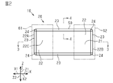
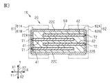
- FIG. 3 is a cross-sectional view taken along line 3-3 of FIG. 2;
- FIG. 3 is an enlarged view of a cross section taken along line 4-4 of FIG. 2;
- Explanatory drawing explaining the manufacturing method of an electronic component Explanatory drawing explaining the manufacturing method of an electronic component.
- Explanatory drawing explaining the manufacturing method of an electronic component Explanatory drawing explaining the manufacturing method of an electronic component.
- Explanatory drawing explaining the manufacturing method of an electronic component Explanatory drawing explaining the manufacturing method of an electronic component.
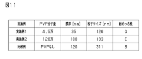
- 4 is a table showing comparison results of electronic components between Examples and Comparative Examples;
- the electronic component 10 is, for example, a surface mount type negative characteristic thermistor component mounted on a circuit board or the like. Negative characteristic thermistor components have the characteristic that the resistance value decreases as the temperature rises.
- the electronic component 10 includes a base body 20.
- the element body 20 has a substantially quadrangular prism shape and has a central axis CA. Note that the axis extending along the central axis CA is referred to as a first axis X hereinafter.
- One of the axes perpendicular to the first axis X is defined as a second axis Y.
- An axis orthogonal to the first axis X and the second axis Y is defined as a third axis Z. As shown in FIG.
- One of the directions along the first axis X is defined as a first positive direction X1, and the direction opposite to the first positive direction X1 among the directions along the first axis X is defined as a first negative direction X2.
- One of the directions along the second axis Y is defined as a second positive direction Y1, and the direction opposite to the second positive direction Y1 among the directions along the second axis Y is defined as a second negative direction Y2.
- one of the directions along the third axis Z is defined as a third positive direction Z1, and the direction opposite to the third positive direction Z1 among the directions along the third axis Z is defined as a third negative direction Z2.
- the outer surface 21 of the base body 20 has six planar planes 22 .
- the term "surface" of the base body 20 as used herein refers to a surface that can be observed when the entire base body 20 is observed. In other words, for example, even if there are minute irregularities or steps that cannot be recognized unless a part of the element body 20 is enlarged and observed with a microscope or the like, it is expressed as a flat surface or a curved surface.
- the six planes 22 extend in different directions.
- the six planes 22 are roughly divided into a first end face 22A facing the first positive direction X1, a second end face 22B facing the first negative direction X2, and four side faces 22C.
- the four side surfaces 22C are a surface facing the third positive direction Z1, a surface facing the third negative direction Z2, a surface facing the second positive direction Y1, and a surface facing the second negative direction Y2. .
- Boundary surface 23 includes a curved surface that exists on the boundary between adjacent flat surfaces 22 . That is, the boundary surface 23 includes a curved surface formed by, for example, rounding the corners forming the adjacent flat surfaces 22 .
- the outer surface 21 of the base body 20 has eight spherical corner surfaces 24 .
- a corner surface 24 is a boundary portion between three adjacent planes 22 .
- the corner surface 24 includes curved surfaces where the three boundary surfaces 23 meet. That is, the corner surface 24 includes, for example, a curved surface formed by R chamfering the corner formed by the three adjacent flat surfaces 22 .
- the surface of the insulating film 50 which will be described later, is identified with the outer surface 21 of the element body 20, and is given reference numerals.
- the dimension along the first axis X of the element body 20 is larger than the dimension along the third axis Z.
- the dimension in the direction along the first axis X of the element body 20 is larger than the dimension in the direction along the second axis Y.
- the material of the element body 20 is ceramics obtained by firing a metal oxide containing at least one of Mn, Fe, Ni, Co, Ti, Ba, Al, and Zn.
- the electronic component 10 has two first internal electrodes 41 and two second internal electrodes 42 .
- the first internal electrodes 41 and the second internal electrodes 42 are embedded inside the element body 20 .
- the material of the first internal electrode 41 is a conductive material.
- the material of the first internal electrode 41 is palladium.
- the material of the second internal electrode 42 is the same as the material of the first internal electrode 41 .
- the shape of the first internal electrode 41 is a rectangular plate.
- the main surface of the first internal electrode 41 is perpendicular to the second Y axis.
- the shape of the second internal electrode 42 is the same rectangular plate shape as the first internal electrode 41 .
- the main surface of the second internal electrode 42 is perpendicular to the second axis Y, like the first internal electrode 41 .
- the dimension of the first internal electrode 41 in the direction along the first axis X is smaller than the dimension in the direction along the first axis X of the element body 20 . Further, as shown in FIG. 1, the dimension of the first internal electrode 41 in the direction along the third axis Z is approximately two thirds of the dimension in the direction along the third axis Z of the element body 20 .
- the dimensions in each direction of the second internal electrodes 42 are the same as the dimensions of the first internal electrodes 41 .
- the first internal electrodes 41 and the second internal electrodes 42 are alternately positioned in the direction along the second Y axis. That is, the first internal electrode 41, the second internal electrode 42, the first internal electrode 41, and the second internal electrode 42 are arranged in this order from the side surface 22C facing the second positive direction Y1 to the second negative direction Y2. In this embodiment, the distances along the second axis Y between the internal electrodes are equal.
- both the two first internal electrodes 41 and the two second internal electrodes 42 are positioned at the center of the element body 20 in the direction along the third axis Z.
- the first internal electrodes 41 are positioned closer to the first positive direction X1.
- the second internal electrode 42 is positioned closer to the first negative direction X2.
- the end of the first internal electrode 41 on the first positive direction X1 side coincides with the end of the element body 20 on the first positive direction X1 side.
- the end of the first internal electrode 41 on the first negative direction X2 side is positioned inside the element body 20 and does not reach the end of the element body 20 on the first negative direction X2 side.
- the end of the second internal electrode 42 on the first negative direction X2 side coincides with the end of the element body 20 on the first negative direction X2 side.
- the end of the second internal electrode 42 on the first positive direction X1 side is located inside the element body 20 and does not reach the end of the element body 20 on the first positive direction X1 side.
- the electronic component 10 has an insulating film 50 .
- the insulating film 50 covers the outer surface 21 of the element body 20 .
- the insulating film 50 covers the entire outer surface 21 of the element body 20 .
- the material of the insulating film 50 is an insulating substance.
- the material of the insulating film 50 is glass. In this embodiment, the glass consists of silicon dioxide.
- the electronic component 10 includes first external electrodes 61 and second external electrodes 62 .
- the first external electrode 61 has a first base electrode 61A and a first metal layer 61B.
- the first base electrode 61A is laminated on the insulating film 50 in a portion of the outer surface 21 of the base body 20 including the first end surface 22A.
- the first base electrode 61A is a five-sided electrode that covers the first end face 22A of the base body 20 and part of the four side faces 22C on the first positive direction X1 side.
- the materials of the first base electrode 61A are silver and glass.
- the first metal layer 61B covers the first base electrode 61A from the outside. Therefore, the first metal layer 61B is stacked on the first base electrode 61A. Specifically, the first metal layer 61B has a two-layer structure of nickel plating and tin plating.
- the second external electrode 62 has a second base electrode 62A and a second metal layer 62B.
- the second base electrode 62A is laminated from above the insulating film 50 on a portion of the outer surface 21 of the base body 20 including the second end surface 22B.
- the second base electrode 62A is a five-sided electrode that covers the second end face 22B of the base body 20 and part of the four side faces 22C on the first negative direction X2 side.
- the material of the second base electrode 62A is the same as the material of the first external electrode 61, which is silver and glass.
- the second metal layer 62B covers the second base electrode 62A from the outside. Therefore, the second metal layer 62B is stacked on the second base electrode 62A. Specifically, like the first metal layer 61B, the second metal layer 62B has a two-layer structure of nickel plating and tin plating.
- the second external electrode 62 does not reach the first external electrode 61 on the side surface 22C, and is arranged away from the first external electrode 61 in the direction along the first axis X.
- the first external electrode 61 and the second external electrode 62 are not laminated on the central portion in the direction along the first axis X, and the insulating film 50 is exposed. 1 to 3, the first external electrode 61 and the second external electrode 62 are illustrated by two-dot chain lines.
- the first external electrode 61 and the end of the first internal electrode 41 on the first positive direction X1 side are connected via a first penetrating portion 71 penetrating through the insulating film 50 .
- the first penetrating portion 71 is formed by extending the palladium forming the first internal electrode 41 toward the first external electrode 61 during the manufacturing process of the electronic component 10 .
- the second external electrode 62 and the end of the second internal electrode 42 on the first negative direction X2 side are connected via a second penetrating portion 72 penetrating through the insulating film 50 .
- the second through portion 72 is also formed by extending the palladium constituting the first internal electrode 41 toward the second external electrode 62 during the manufacturing process of the electronic component 10 .
- FIG. 3 illustrates the first internal electrode 41 and the first through portion 71 as separate members having a boundary, there is actually no clear boundary between them. In this regard, the same applies to the second through portion 72 . 1 and 2, illustration of the first through portion 71 is omitted.
- the base body 20 has cracks 26 .
- Crack 26 has an opening 27 that opens to outer surface 21 .
- the tip of the crack 26 is positioned inside the element body 20 .
- the cross section CS shown in FIG. 4 is parallel to both the second Y axis and the third Z axis.
- FIG. 4 shows an enlarged view of a portion of the cross section CS including the side surface 22C facing the third positive direction Z1. Therefore, the cross section CS is orthogonal to the planar side surface 22C of the outer surface 21 facing the third positive direction Z1. Further, an orthogonal axis orthogonal to the side surface 22C facing the third positive direction Z1 is parallel to the third axis Z.
- the cross-section CS shown in FIG. 4 is a cross-sectional view perpendicular to the side surface 22C.
- the outer surface 21 of the base body 20 has fine unevenness. Therefore, as shown in FIG. 4, the side surface 22C also has fine unevenness. However, each side surface 22C of the outer surface 21 extends in parallel with the central axis CA even if it has minute irregularities that cannot be confirmed unless observed with a microscope or the like.
- crack 26 has first portion 26A including opening 27 .
- the crack 26 consists only of the first portion 26A.
- the straight line passing through the center of the opening 27 and the tip of the crack 26 is defined as the growth axis AX.
- the direction in which the first portion 26A extends is the direction from the opening 27 to the tip of the first portion 26A on the extension axis AX.
- the extension axis AX along the direction in which the first portion 26A extends extends in a direction that intersects the third axis Z, which is an orthogonal axis.
- an acute angle C of angles formed by the extension axis AX and the second axis Y which is an axis along the direction in which the side surface 22C extends, is less than 45 degrees.
- the acute angle C of the angle formed by the progression axis AX and the first axis X is less than 15 degrees. Therefore, the crack 26 extends substantially parallel to the side surface 22C.
- the width dimension of the first portion 26A is maximum at the opening 27.
- the maximum value WM of the width dimension of the first portion 26A is less than twice the film thickness, which is the average value of the thickness dimension of the insulating film 50 in the direction perpendicular to the outer surface 21 .
- the width dimension of the first portion 26A is the length of the shortest line segment that can be drawn from an arbitrary point on the inner wall of the first portion 26A to the opposite inner wall on the cross section CS.
- the film thickness, which is the average value of the thickness dimension of the insulating film 50 in the direction perpendicular to the outer surface 21, is the average value of the three measured thickness dimensions of the insulating film 50 in the cross section CS. .
- a portion of the insulating film 50 enters the internal space of the first portion 26A. Further, part of the insulating film 50 fills the internal space of the crack 26 . That a part of the insulating film 50 fills the internal space of the crack 26 means that the porosity of the internal space of the crack 26 is 10% or less in the cross section CS.
- the porosity is calculated, for example, by creating an image of the cross section CS showing mapping data of the glass component, which is the main component of the insulating film 50 , and the main component of the element body 20 .
- an electron microscope SEM
- an EDX image showing the EDX mapping data of the main component of the element body 20 and an EDX image showing the EDX mapping data of the main component of the glass are obtained for the portion of the cross section CS where the crack 26 exists.
- a field emission transmission electron microscope FE-TEM
- JEOL JEM-F200 manufactured by JEOL Ltd. and an analysis system Norman system 7 manufactured by Thermo Fisher Scientific were used.
- each acquired EDX image is taken out as a CSV file.
- the numerical data contained in the CSV file is matrix-like numerical data.
- the matrix-like numerical data is, for example, matrix-like numerical data of 256 rows ⁇ 256 columns. Each of such numerical data corresponds to the intensity in each of the small sections obtained by dividing the range of the EDX image into 256 in the vertical direction and 256 in the horizontal direction. It should be noted that if the matrix-like numerical data is output in the form of spreadsheet software, for example, the processing of the subsequent procedures is facilitated.
- the maximum value of the numerical data included in the CSV file is determined, and using the maximum value, a value obtained by dividing 100 by the maximum value so that the maximum value becomes 100 is calculated as a coefficient. All numerical data in the CSV file are multiplied by the calculated coefficient. As a result, all numerical data can be normalized so that the maximum value of the numerical data is 100.
- a location where the strength of the main component of the glass in the range of the crack 26 is 10 or more is selected.
- the range of this selected location is the range filled with glass.
- the number of pixels where the strength of the main component of the glass is less than 10 within the range of the cracks 26 is calculated.
- the porosity is calculated by dividing the number of pixels where the strength of the main component of the glass is less than 10 by the number of pixels within the range of the cracks 26 . It is said that part of the insulating film 50 fills the internal space of the crack 26 when the porosity calculated in this way is 10% or less.
- the electronic component 10 having an average value of 100 nm in the thickness direction of the insulating film 50 was evaluated for the presence or absence of breakage by the impact test.
- the impact test is a test in which a predetermined constant impact is applied to electronic component 10 .
- the method for manufacturing the electronic component 10 includes a laminate preparation step S11, an R chamfering step S12, a solvent charging step S13, a catalyst charging step S14, an element charging step S15, and a polymer charging step S15.
- a step S16 and a metal alkoxide introduction step S17 are provided.
- the method for manufacturing the electronic component 10 further includes a film forming step S18, a drying step S19, a conductor coating step S20, a curing step S21, and a plating step S22.
- a layered body that is the element body 20 without the boundary surface 23 and the corner surface 24 is prepared. That is, the laminated body is in a state before R-chamfering and has a rectangular parallelepiped shape having six planes 22 .
- a plurality of ceramic sheets to be the element body 20 are prepared. The sheet is a thin plate. A conductive paste to be the first internal electrodes 41 is laminated on the sheet. A ceramic sheet to be the element body 20 is laminated on the lamination paste. A conductive paste that becomes the second internal electrode 42 is laminated on the sheet. Thus, the ceramic sheet and the conductive paste are laminated. Then, by cutting into a predetermined size, an unfired laminate is formed. After that, the laminate is prepared by baking the unbaked laminate at a high temperature.
- the R chamfering process S12 is performed.
- the boundary surface 23 and the corner surface 24 are formed in the laminate prepared in the laminate preparation step S11.
- the corners of the laminated body are chamfered by barrel polishing to form a boundary surface 23 having a curved surface and a corner surface 24 having a curved surface.
- the element body 20 is formed.
- cracks 26 are formed in the element body 20 due to the impact caused by the barrel polishing.
- solvent injection step S13 is performed.
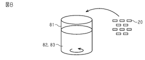
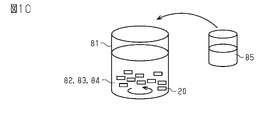
- 2-propanol is charged as a solvent 82 into the reaction vessel 81.
- a catalyst charging step S14 is performed.
- stirring of the solvent 82 in the reaction vessel 81 is first started.
- ammonia water is put into the reaction vessel 81 as an aqueous solution 83 containing a catalyst.
- the catalyst in this embodiment is hydroxide ions, and functions as a catalyst that promotes hydrolysis of metal alkoxide 85, which will be described later.
- the element loading step S15 is performed. As shown in FIG. 8, in the element loading step S15, a plurality of elements 20 formed in advance in the R-chamfering step S12 as described above are loaded into the reaction vessel 81 .
- the polymer charging step S16 is performed.
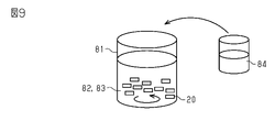
- polyvinylpyrrolidone is charged as the polymer 84 into the reaction vessel 81 .
- the polymer 84 put into the reaction vessel 81 is adsorbed on the outer surface 21 of the element body 20 .
- a metal alkoxide introduction step S17 is performed.
- liquid tetraethyl orthosilicate is charged into the reaction vessel 81 as the metal alkoxide 85 .
- Tetraethyl orthotetrasilicate is sometimes called tetraethoxysilane.
- the amount of the metal alkoxide 85 to be introduced in the metal alkoxide introduction step S17 is calculated based on the area of the outer surface 21 of the element 20 introduced in the element introduction step S15. Specifically, it is calculated by multiplying the amount of metal alkoxide 85 per element body 20 necessary for forming the insulating film 50 covering the outer surface 21 of the element body 20 by the number of element bodies 20 . .
- a film forming step S18 is performed.
- stirring of the solvent 82 started in the solvent charging step S13 is continued for a predetermined time after the metal alkoxide 85 is charged into the reaction vessel 81 in the metal alkoxide charging step S17.
- the insulating film 50 is formed by a liquid phase reaction within the reaction vessel 81.
- the metal alkoxide 85 and the like contained in the solvent 82 flow into the internal space of the crack 26 because they are in the liquid phase.
- the insulating film 50 is also formed on the inner wall of the crack 26 by the liquid phase reaction.
- the drying step S19 is performed.
- the element body 20 is taken out from the reaction vessel 81 and dried.
- the sol-like insulating film 50 is dried and turned into a gel-like insulating film 50 .
- the element body is formed by the solvent charging step S13, the catalyst charging step S14, the element charging step S15, the polymer charging step S16, the metal alkoxide charging step S17, and the film forming step S18.
- a film forming method for forming an insulating film 50 on 20 is configured.
- the conductor coating step S20 is performed.
- two portions of the surface of the insulating film 50 one including the portion covering the first end surface 22A of the element body 20 and the other including the portion covering the second end surface 22B of the element body 20, are coated.
- Apply conductive paste to Specifically, the conductive paste is applied so as to cover the insulating film 50 on the entire first end face 22A and part of the four side faces 22C. Also, the conductive paste is applied so as to cover the insulating film 50 on the entire second end face 22B and part of the four side faces 22C.
- the curing step S21 is performed. Specifically, in the curing step S21, the insulating film 50 and the element body 20 coated with the conductor paste are heated. As a result, the water and the polymer 84 are vaporized from the gel-like insulating film 50, thereby baking and hardening the insulating film 50 covering the outer surface 21 of the element body 20, as shown in FIG. At the same time, the first base electrode 61A and the second base electrode 62A are formed by baking the conductor paste applied in the conductor applying step S20. In this manner, the base electrode forming process is composed of the conductor coating process S20 and the curing process S21. That is, in the present embodiment, the curing step S21 serves not only as a step of curing the insulating film 50 but also as part of the underlying electrode forming step.
- the first base electrode 61A containing silver The palladium contained on the first internal electrode 41 side is attracted.
- the first penetrating portion 71 extends through the insulating film 50 from the first internal electrode 41 toward the first base electrode 61A, thereby connecting the first internal electrode 41 and the first base electrode 61A.
- the plating step S22 is performed. Electroplating is performed on the portions of the first base electrode 61A and the second base electrode 62A. Thereby, the first metal layer 61B is formed on the surface of the first base electrode 61A. A second metal layer 62B is formed on the surface of the second base electrode 62A. Although not shown, the first metal layer 61B and the second metal layer 62B are electroplated with two kinds of nickel and tin to form a two-layer structure. Thus, the electronic component 10 is formed.
- the molecular weight of polyvinylpyrrolidone used as the polymer 84 is 45,000.
- the polyvinylpyrrolidone used as the polymer 84 has a molecular weight of 1,200,000.
- the electronic component of the comparative example did not use the polymer 84 and was manufactured without the polymer introduction step S16.
- the electronic component 10 of Examples 1 and 2 and the electronic component of the comparative example were manufactured using the same amount of metal alkoxide 85 .
- the film thickness of the insulating film 50 was measured for the electronic components 10 of Examples 1 and 2 and the electronic component of the comparative example.
- the film thickness of the insulating film 50 was measured at a cross section CS passing through the center of the base body 20 in the direction along the first axis X and perpendicular to the central axis CA. In the cross section CS shown in FIG. film thickness.
- the film thickness of the insulating film 50 was 35 nm. In the electronic component 10 of Example 2, the film thickness of the insulating film 50 was 100 nm. In the electronic component of the comparative example, the film thickness of the insulating film 50 was 120 nm.
- the particle size of the glass particles present on the surface of the insulating film 50 was measured for the electronic components 10 of Examples 1 and 2 and the electronic component of the comparative example.
- the grain size is the size of glass grains that are present on the surface of the insulating film 50 at a certain rate or more.
- the surface of the portion of the side surface 22C not covered with the first external electrode 61 and the second external electrode 62 was observed with an electron microscope. Then, the average value of the diameters of the particles was calculated, excluding large particles in which a plurality of particles present in very small numbers were gathered in the observed range.
- the particle size was 126 nm. In the electronic component 10 of Example 2, the particle size was 193 nm. In the electronic component of the comparative example, the particle size was 311 nm.
- Plating resistance is a property that prevents the base body 20 from dissolving in a plating solution.
- the plating solution is used when forming the first external electrode 61 and the second external electrode 62 .
- an evaluation sample was obtained by forming the insulating film 50 and the first base electrode 61A and the second base electrode 62A on the element body 20 .
- the evaluation sample is plated with nickel. At least two adjacent outer surfaces 21 of the nickel-plated evaluation sample are photographed under ring illumination.
- the area ratio of the portion where the element body is eluted is measured on each surface by image processing, and the average value is calculated.
- E Excellent
- G Good
- B Bad
- the plating resistance was G (Good). In the electronic component 10 of Example 2, the plating resistance was E (Excellent). In the electronic component of the comparative example, the plating resistance was B (Bad).
- the glass particles grow relatively quickly and the particle size increases. Then, it is considered that the film thickness of the insulating film 50 is increased because the glass particles having a large particle size successively adhere to the surface of the element body 20 .
- the electronic component 10 of Example 1 when comparing the difference in molecular weight of the polymer 84, when the molecular weight of the polymer 84 is small, the polymer 84 is densely packed in the same size space as compared to when the molecular weight is large. Therefore, it is considered that the growth of the glass particles was more likely to be inhibited. As a result, the electronic component 10 of Example 1, in which the polymer 84 has a small molecular weight, has a smaller particle size and a smaller film thickness than the electronic component 10 of Example 2.
- the particle size of the glass particles is the same, the larger the film thickness, the more likely the plating resistance will be secured. discovered to be This is because when the particle size is excessively large, when an impact from the outside of the element body 20 is applied to the vicinity of the particles of glass having a large particle size, the particles move the neighboring insulating film 50 from the outer surface 21 of the element body 20 . It is thought that it may be peeled off. Therefore, the electronic component 10 of Example 2, in which the particle size is appropriately suppressed and the film thickness is increased, is preferable from the viewpoint of plating resistance.
- the acute angle C among the angles formed by the side surface 22C and the extension axis AX along the direction in which the first portion 26A extends is less than 15 degrees. Therefore, part of the insulating film 50 enters the first portion 26A of the crack 26 extending in a direction that tends to cause partial peeling of the element body 20 . Therefore, it is possible to suitably suppress partial peeling of the base body 20 due to the progress of the crack 26 .
- the maximum value WM of the width dimension of the first portion 26A is twice or less the average value of the thickness direction of the insulating film 50 in the direction perpendicular to the side surface 22C. . Therefore, the film thickness of the insulating film 50 is sufficiently large with respect to the width dimension of the first portion 26A of the crack 26 . That is, the insulating film 50 has a sufficient amount to fill the internal space of the crack 26 . Therefore, it is easy to secure the amount of the insulating film 50 entering the internal space of the crack 26 .
- the material of the element body 20 is ceramics. Therefore, cracks 26 are likely to occur in the element body 20 during the manufacturing process. As a result, the insulation film 50 enters the inner space of the crack 26, and the effect of suppressing chipping or the like of the element body 20 can be obtained remarkably.
- the metal alkoxide 85 and the like contained in the solvent 82 flow into the crack 26 in liquid phase. Therefore, the insulating film 50 can be formed inside the cracks 26 in the film forming step S18 without adjusting the spray direction of the glass slurry or controlling the particle size of the glass slurry in the manufacturing process.
- the electronic component 10 is not limited to the negative characteristic thermistor component.
- it may be a thermistor component with a non-negative characteristic, a multilayer capacitor component, or an inductor component.
- the material of the element body 20 is not limited to the example of the above embodiment.
- the material of the base body 20 may be a composite of resin and metal powder.
- the shape of the base body 20 is not limited to the example of the above embodiment.
- the base body 20 may have a polygonal columnar shape other than a quadrangular columnar shape having the central axis CA.
- the element body 20 may be the core of a wire-wound inductor component.
- the core may be in the shape of a so-called drum core.
- the core may have a columnar winding core and flanges provided at each end of the winding core.
- the outer surface 21 of the base body 20 may not have a corner surface 24 including a curved surface.
- a corner surface 24 including a curved surface may not exist at the location where three such boundaries intersect.
- the crack 26 may have other portions in addition to the first portion 26A.
- the crack 26 has, in the cross section CS, a first portion 26A extending across the orthogonal third axis Z, and a crack connecting to the first portion 26A and extending in a direction different from the first portion 26A. and a second portion extending therealong.
- the second portion may extend along the third axis Z, which is an orthogonal axis.
- an axis of progression AX passing through the center of the opening 27 of the crack 26 and an arbitrary point of the crack 26 is drawn. Then, while gradually moving an arbitrary point of the crack 26 away from the opening 27, the propagation axis AX is similarly drawn. In this way, a large number of propagation axes AX are drawn, and the point of the crack 26 when the propagation axis AX is parallel to the second axis Y is first determined as a specific point.
- the first portion 26A of the crack 26 extends from the center of the opening 27 of the crack 26 to the specific point (but not including the specific point).
- the first portion 26A is the portion up to the portion positioned directly below the opening 27 of the crack 26 in the direction along the second axis Y, excluding the specific point. If the extension axis AX is not parallel to the second axis Y even if the arbitrary point is moved to the tip of the crack 26, the crack 26 as a whole is the first portion 26A as in the above embodiment. be.
- the acute angle C among the angles formed by the side surface 22C and the progression axis AX may be 15 degrees or more. If the acute angle C is less than 45 degrees, it is difficult for the glass slurry to enter the cracks 26 in a manufacturing method in which the insulating film 50 is formed by spraying glass slurry. In this regard, the manufacturing method of the above-described embodiment is more preferable because the reaction progresses in the first portion 26A of the crack 26 and the insulating film 50 is formed. Further, even if the acute angle C is 45 degrees or more, part of the insulating film 50 enters the cracks 26, so that the element body 20 is less likely to be damaged.
- the maximum value WM of the width dimension of the first portion 26A may be larger than twice the average value of the insulating film 50 in the thickness direction. At least a part of the insulating film 50 needs to enter the first portion 26A.
- the width dimension of the first portion 26A may be maximum outside the opening 27 . That is, the maximum value WM of the width dimension of the first portion 26A may be the width dimension of a portion other than the opening 27.
- first internal electrode 41 and the second internal electrode 42 does not matter as long as it can ensure electrical continuity with the corresponding first external electrode 61 and second external electrode 62 .
- the number of first internal electrodes 41 and second internal electrodes 42 is not limited, and the number of first internal electrodes 41 may be one, or three or more.
- the configuration of the first external electrode 61 is not limited to the example of the above embodiment.
- the first external electrode 61 may be composed of only the first base electrode 61A, and the first metal layer 61B may not have a two-layer structure.
- the insulating film 50 covers the entire outer surface 21 of the element 20, thereby suppressing dissolution of the element 20 in the plating solution. effect is obtained.
- the combination of materials for the first internal electrode 41 and the first base electrode 61A is not limited to the combination of palladium and silver.
- it may be a combination of copper and nickel, copper and silver, silver and gold, nickel and cobalt, or nickel and gold.
- one may be silver and the other may be a combination of silver and palladium.
- one may be palladium and the other may be a combination of silver and palladium, or one may be copper and the other may be a combination of silver and palladium.
- one may be gold and the other may be a combination of silver and palladium.
- the Kirkendall effect may not be obtained depending on the combination of the first internal electrode 41 and the first base electrode 61A.
- part of the insulating film 50 is physically removed by polishing the first end face 22A side of the element body 20, for example, so that the first internal electrode 41 is exposed. do it.
- the first internal electrode 41 and the first base electrode 61A can be connected.
- the insulating film 50 may be formed including the surface of the first base electrode 61A, and the insulating film 50 covering the surface of the first base electrode 61A may be removed.
- the arrangement location of the first external electrode 61 is not limited to the example of the above embodiment.
- the first external electrode 61 may be arranged only on the first end surface 22A and one side surface 22C. In this regard, the same applies to the second external electrode 62 as well.
- the insulating film 50 does not have to cover the entire area of the outer surface 21 of the element body 20 . That is, a portion of the outer surface 21 of the element body 20 may be exposed from the insulating film 50 .
- the range covered by the insulating film 50 may be appropriately changed according to the shape of the element body 20, the positions of the first external electrode 61 and the second external electrode 62, and the like.
- the glass in the insulating film 50 may be integrated with the glass in the first base electrode 61A by diffusing.
- the material of the insulating film 50 is not limited to the example of the above embodiment.
- the glass is not limited to silicon dioxide, and may be a multi-component oxide containing Si, such as B—Si, Si—Zn, Zr—Si, or Al—Si oxides. good too.
- the glass may also be a multi-component oxide containing alkali metals and Si, such as Al—Si, Na—Si, K—Si, and Li—Si oxides.
- the glass may be a multicomponent oxide containing alkaline earth metals and Si such as Mg--Si, Ca--Si, Ba--Si and Sr--Si.
- the glass may be Si-free or a mixture thereof.
- the material of the insulating film 50 may contain a pigment, a silicone-based flame retardant, a silane coupling agent, a titanate coupling agent, or other surface treatment agent or antistatic agent.
- the insulating film 50 may contain additives such as organic acid salts, oxides, inorganic salts, organic salts, fine particles of other metal oxides, and nanoparticles.
- organic acid salts include oxoacid salts such as soda ash, sodium carbonate, sodium hydrogen carbonate, sodium percarbonate, sodium sulfite, sodium hydrogen sulfite, sodium sulfate, sodium thiosulfate, sodium nitrate, sodium sulfite, and sodium fluoride. , sodium chloride, sodium bromide, and sodium iodide.
- oxides include sodium peroxide
- hydroxides include sodium hydroxide
- Inorganic salts include, for example, sodium hydride, sodium sulfide, sodium hydrogen sulfide, sodium silicate, trisodium phosphate, sodium borate, sodium borohydride, sodium cyanide, sodium cyanate, sodium tetrachloroaurate. .
- inorganic salts include calcium peroxide, calcium hydroxide, calcium fluoride, calcium chloride, calcium bromide, calcium iodide, calcium hydride, calcium carbide, and calcium phosphide.
- Additives include calcium carbonate, calcium hydrogen carbonate, calcium nitrate, calcium sulfate, calcium sulfite, calcium silicate, calcium phosphate, calcium pyrophosphate, calcium hypochlorite, calcium chlorate, calcium perchlorate, and calcium bromate. , calcium iodate, calcium arsenite, calcium chromate, calcium tungstate, calcium molybdate, calcium magnesium carbonate, hydroxyapatite.
- Additives include calcium acetate, calcium gluconate, calcium citrate, calcium malate, calcium lactate, calcium benzoate, calcium stearate, and calcium aspartate.
- additives include lithium carbonate, lithium chloride, lithium titanate, lithium nitride, lithium peroxide, lithium citrate, lithium fluoride, lithium hexafluorophosphate, lithium acetate, lithium iodide, lithium hypochlorite. , lithium tetraborate, lithium bromide, lithium nitrate, lithium hydroxide, lithium aluminum hydride, lithium triethylborohydride, lithium hydride, lithium amide, lithium imide, lithium diisopropylamide, lithium tetramethylpiperidide, sulfide It may be lithium, lithium sulfate, lithium thiophenolate, lithium phenoxide.
- the additive may be boron triiodide, sodium cyanoborohydride, sodium borohydride, tetrafluoroboric acid, triethylborane, borax, and boric acid.
- the additive is potassium arsenide, potassium bromide, potassium carbide, potassium chloride, potassium fluoride, potassium hydride, potassium iodide, potassium triiodide, potassium azide, potassium nitride, potassium superoxide, ozone Potassium chloride, potassium peroxide, potassium phosphide, potassium sulfide, potassium selenide, potassium telluride, potassium tetrafluoroaluminate, potassium tetrafluoroborate, potassium tetrahydroborate, potassium methanide, potassium cyanide, potassium formate, fluoride Potassium hydrogen, te, potassium rayodomercuric acid (II), potassium hydrogen sulfide, potassium octachlorodimolybdate (II), potassium amide, potassium hydroxide, potassium hexafluorophosphate, potassium carbonate, potassium tetrachloride platinate (II) , potassium hexachloridoplatinate
- additives include barium sulfite, barium chloride, barium chlorate, barium perchlorate, barium peroxide, barium chromate, barium acetate, barium cyanide, barium bromide, barium oxalate, barium nitrate, hydroxide Barium, barium hydride, barium carbonate, barium iodide, barium sulfide, barium sulfate may be used.
- Other additives may be sodium acetate and sodium citrate.
- the additive may also be fine particles or nanoparticles of metal oxides.
- metal oxides include sodium oxide, calcium oxide, lithium oxide, boron oxide, potassium oxide, barium oxide, silicon oxide, , titanium oxide, zirconium oxide, aluminum oxide, zinc oxide and magnesium oxide.
- the metal alkoxide 85 is not limited to the example of the above embodiment.
- Elements capable of synthesizing the metal alkoxide 85 include, for example, Li, Be, B, C, Na, Mg, Al, Si, P, K, Ca, Sc, Ti, V, Cr, Mn, Fe, Co, Ni , Cu, Zn, Ga, Ge, As, Rb, Sr, Y, Zr, Nb, Mo, Cd, In, Sn, Sb, Cs, Ba, La, Ce, Pr, Nd, Pm, Sm, Eu, Gd , Tb, Dy, Ho, Er, Tm, Yb, Lu, Hf, Ta, W, Hg, Tl, Pb, Bi, Th, Pa, U, and Pu. Alkoxides of these elements can be used as precursors for glasses.
- Metal alkoxide 85 is, for example, sodium methoxide, sodium ethoxide, calcium diethoxide, lithium isopropoxide, lithium ethoxide, lithium tert-butoxide, lithium methoxide, boron alkoxide, potassium t-butoxide, tetraethyl orthosilicate, allyltrimethoxysilane, isobutyl(trimethoxy)silane, tetrapropyl orthosilicate, tetramethyl orthosilicate, [3-(diethylamino)propyl]trimethoxysilane, triethoxy(octyl)silane, triethoxyvinylsilane, triethoxyphenylsilane, trimethoxy phenylsilane, trimethoxymethylsilane, butyltrichlorosilane, n-propyltriethoxysilane, methyltrichlorosilane, dime
- a metal complex or acetate which is a precursor of the metal alkoxide 85, may be used instead of the metal alkoxide 85.
- a metal complex or acetate as a metal alkoxide precursor may be introduced.
- metal complexes include lithium acetylacetonate, titanium (IV) oxyacetylacetonate, titanium diisopropoxide bis(acetylacetonate), zirconium (IV) trifluoroacetylacetonate, and zirconium (IV) acetylacetonate.
- acetates include zirconium acetate, zirconium(IV) acetate hydroxide, and basic aluminum acetate.
- the base electrode forming step is not limited to the example of the above embodiment.
- the insulating film 50 is hardened by heat treatment, and then the conductor coating step S20 and the hardening step S21 are performed. may be formed.
- the first external electrode 61 may be formed on the exposed portion by a plating method. good.
- the curing step S21 is not limited to the step of simultaneously curing the insulating film 50 and the conductor paste.
- the conductor paste is a material that is cured by ultraviolet irradiation
- a heating process may be performed as the curing process for curing the insulating film 50
- ultraviolet irradiation may be performed as the process for curing the conductor paste.
- the insulating film 50 may be cured by sufficiently vaporizing the water and the polymer 84 in the drying step S19.
- the drying step S ⁇ b>19 functions as a curing step for curing the insulating film 50 .
- the order of the solvent charging step S13, the catalyst charging step S14, and the element charging step S15 does not matter.
- the reaction between the metal alkoxide 85 and the catalyst should be started in the reaction vessel 81 in a state in which the solvent 82 , the element 20 and the polymer 84 are put into the reaction vessel 81 .
- the polymer 84 is not limited to polyvinylpyrrolidone.
- polymer 84 may be an acrylic homopolymer or copolymer of acrylic acid, methacrylic acid, or their esters.
- acrylic materials include acrylic acid ester copolymers, methacrylic acid ester copolymers, and acrylic acid ester-methacrylic acid ester copolymers.
- the polymer 84 may be a homopolymer or copolymer of cellulose, polyvinyl alcohol, polyvinyl acetate, polyvinyl chloride, polypropylene carbonate, or the like.
- Cellulose-based materials include, for example, hydroxypropylcellulose, cellulose ether, carboxymethylcellulose, acetylcellulose, and acetylnitrocellulose.
- the polymer 84 may contain a plurality of types, as long as it contains at least one selected from the exemplified ones.
- the solvent 82 is not limited to 2-propanol.
- the solvent 82 may be appropriately changed as long as the metal alkoxide 85 can be sufficiently dispersed.
- the film forming method described in JP-A-2020-36002 includes a solvent charging step, a catalyst charging step, an element charging step, and a metal alkoxide charging step. Moreover, the said film-forming method is provided with the film-forming process. In the film forming process, an insulating film made of silicon oxide is formed on the outer surface of the element by hydrolysis and polycondensation reaction of the metal alkoxide.
- the size of the silicon oxide may become excessively large in the film formation process. If large-sized silicon oxide particles are present on the surface of the insulating film, when an impact from the outside of the element is applied to the vicinity of the particles, the particles will damage the insulating film in the vicinity of the outer surface of the element. It may peel off from the
- the polymer 84 is introduced in the polymer introduction step S16.
- the polymer 84 is adsorbed to the outer surface 21 of the base body 20 .
- the glass microparticles derived from the metal alkoxide 85 are incorporated into the polymer 84 in the metal alkoxide introduction step S17. Coarse particles of glass that have grown excessively large cannot be incorporated into the polymer 84 .
- the insulating film 50 does not contain excessively large particles.
- the cracks 26 in the element body 20 are not essential. Also, the crack 26 in the element body 20 does not have to be partly intruded into the insulating film 50 .
- the size of the coarse glass particles can be made smaller.
Landscapes
- Engineering & Computer Science (AREA)
- Microelectronics & Electronic Packaging (AREA)
- Power Engineering (AREA)
- Physics & Mathematics (AREA)
- Electromagnetism (AREA)
- Ceramic Engineering (AREA)
- Manufacturing & Machinery (AREA)
- Fixed Capacitors And Capacitor Manufacturing Machines (AREA)
- Coils Or Transformers For Communication (AREA)
Abstract
Description
以下、電子部品の一実施形態を、図面を参照して説明する。なお、図面は、理解を容易にするために構成要素を拡大して示している場合がある。構成要素の寸法比率は実際のものと、又は別の図面中のものと異なる場合がある。また、断面図ではハッチングを付しているが、理解を容易にするために一部の構成要素のハッチングを省略している場合がある。
図1に示すように、電子部品10は、例えば、回路基板等に実装される表面実装型の負特性サーミスタ部品である。なお、負特性サーミスタ部品は、温度が上がると抵抗値が下がるという特性を有するものである。
図2に示すように、素体20は、第1軸Xに沿う方向の寸法が、第3軸Zに沿う方向の寸法よりも大きい。また、図1に示すように、素体20は、第1軸Xに沿う方向の寸法が、第2軸Yに沿う方向の寸法よりも大きい。また、素体20の材質は、Mn、Fe、Ni、Co、Ti、Ba、Al、及びZnの少なくとも1つを成分とする金属酸化物を焼成したセラミックスである。
図4に示すように、素体20は、クラック26を有している。クラック26は、外表面21に開口する開口27を有している。クラック26の先端は、素体20の内部に位置している。
絶縁膜50の一部がクラック26の内部空間を埋めているとは、断面CSにおいて、クラック26の内部空間の空隙率が、10%以下であることをいう。空隙率は、例えば、断面CSの画像を、絶縁膜50の主成分であるガラスの成分と素体20の主成分とのマッピングデータを示す画像を作成することで算出する。
絶縁膜50の厚さ方向の平均値を100nmとする電子部品10について、衝撃試験による破損の有無を評価した。衝撃試験は、電子部品10に対して、予め定められた一定の衝撃を加える試験である。
(全体構成について)
次に、電子部品10の製造方法について説明する。
次に、図5に示すように、触媒投入工程S14を行う。図7に示すように、触媒投入工程S14では、先ず、反応容器81内の溶媒82の撹拌を開始する。そして、反応容器81内に、触媒を含む水溶液83として、アンモニア水を投入する。この実施形態における触媒は、水酸化物イオンであり、後述する金属アルコキシド85の加水分解を促進する触媒として機能する。
ここで、上述した製造方法によって製造した電子部品10の実施例1及び実施例2と、比較例の電子部品とについて、絶縁膜50の膜厚、絶縁膜50の表面に存在するガラス粒子の粒子サイズ及び耐めっき性を比較した。
上述したように、ポリマー84の分子量の違いによって、絶縁膜50の膜厚、ガラスの粒子の粗粒サイズ及び耐めっき性が変化することを、発明者らは発見した。そこで、ポリマー84の分子量の違いによる成膜過程について、考察した。
仮に、絶縁膜50の一部がクラック26の内部空間に入り込まずに、クラック26の内部空間が空隙になっているとする。この場合、電子部品10の外部から衝撃が加わると、その衝撃がクラック26の先端に集中して作用することがある。この場合、クラック26の先端からき裂が進展する。すると、クラック26を挟んだ両側の部分が引き離されるように、素体20の割れが発生する。
(1)上記実施形態によれば、絶縁膜50の一部は、クラック26の内部空間に入り込んでいる。そのため、電子部品10に外部から衝撃が加わったとき、その衝撃は、クラック26の内部空間に存在する絶縁膜50に受け止められる。したがって、外部からの衝撃が、クラック26の先端に集中して作用することは抑制され、クラック26の進展を防げる。
上記実施形態は以下のように変更して実施することができる。上記実施形態及び以下の変更例は、技術的に矛盾しない範囲で組み合わせて実施することができる。
・素体20の形状は、上記実施形態の例に限られない。例えば、素体20は、中心軸線CAを有する四角形柱状以外の多角形柱状であってもよい。また、素体20は、巻線型のインダクタ部品のコアであってもよい。例えば、コアは、いわゆるドラムコア形状であってもよい。具体的には、コアは、柱状の巻芯部と、巻芯部の各端部に設けられた鍔部とを有していてもよい。
有機酸塩としては、例えば、ソーダ灰、炭酸ナトリウム、炭酸水素ナトリウム、過炭酸ナトリウム、亜硫酸ナトリウム、亜硫酸水素ナトリウム、硫酸ナトリウム、チオ硫酸ナトリウム、硝酸ナトリウム、亜硫酸ナトリウムといったオキソ酸の塩やフッ化ナトリウム、塩化ナトリウム、臭化ナトリウム、ヨウ化ナトリウムといったハロゲン化合物が挙げられる。
無機塩としては、例えば、水素化ナトリウム、硫化ナトリウム、硫化水素ナトリウム、珪酸ナトリウム、リン酸三ナトリウム、ほう酸ナトリウム、水素化ホウ素ナトリウム、シアン化ナトリウム、シアン酸ナトリウム、テトラクロロ金酸ナトリウムが挙げられる。
<付記1>
素体の外表面に金属酸化物を含む絶縁膜を成膜する成膜方法であって、
反応容器内に前記素体を投入する素体投入工程と、
前記反応容器内に、前記素体の外表面に吸着するポリマーを投入するポリマー投入工程と、
前記容器内に金属アルコキシド又は金属アルコキシド前駆体を投入する金属アルコキシド投入工程と、
前記反応容器内に、前記金属アルコキシドの加水分解を促進する触媒を投入する触媒投入工程と、
前記金属アルコキシドを加水分解及び脱水縮合して前記素体の外表面に前記絶縁膜を製膜する成膜工程と、を備える
成膜方法。
20…素体
21…外表面
26…クラック
26A…第1部分
27…開口
41…第1内部電極
42…第2内部電極
50…絶縁膜
61…第1外部電極
62…第2外部電極
71…第1貫通部
72…第2貫通部
81…反応容器
82…溶媒
83…水溶液
84…ポリマー
85…金属アルコキシド
85A…ガラス微粒子
85B…ガラス粗大粒子
Claims (5)
- 平面を含む外表面を有する素体と、前記外表面を覆う絶縁膜と、を備え、
前記素体は、前記外表面に開口するクラックを有し、
前記平面に直交する断面視において、前記クラックは、前記開口から前記平面に直交する直交軸に交差して延びている第1部分を有し、
前記絶縁膜の一部は、前記第1部分の内部空間に入り込んでいる
電子部品。 - 前記平面に直交する断面視において、前記平面と前記第1部分が延びる方向に沿う進展軸とがなす角のうち鋭角は、45度未満である
請求項1に記載の電子部品。 - 前記平面に直交する断面視において、前記平面と前記進展軸とがなす角のうち鋭角は、15度未満である
請求項2に記載の電子部品。 - 前記平面に直交する断面視において、前記第1部分の幅寸法の最大値は、前記絶縁膜における前記外表面に直交する方向の厚さ寸法の平均値の2倍以下である
請求項1~請求項3のいずれか1項に記載の電子部品。 - 前記素体の材質は、セラミックスである
請求項1~請求項4のいずれか1項に記載の電子部品。
Priority Applications (3)
| Application Number | Priority Date | Filing Date | Title |
|---|---|---|---|
| CN202280042513.1A CN117501390A (zh) | 2021-06-15 | 2022-03-30 | 电子部件 |
| JP2023529617A JPWO2022264635A1 (ja) | 2021-06-15 | 2022-03-30 | |
| US18/475,294 US20240021346A1 (en) | 2021-06-15 | 2023-09-27 | Electronic component |
Applications Claiming Priority (2)
| Application Number | Priority Date | Filing Date | Title |
|---|---|---|---|
| JP2021-099718 | 2021-06-15 | ||
| JP2021099718 | 2021-06-15 |
Related Child Applications (1)
| Application Number | Title | Priority Date | Filing Date |
|---|---|---|---|
| US18/475,294 Continuation US20240021346A1 (en) | 2021-06-15 | 2023-09-27 | Electronic component |
Publications (1)
| Publication Number | Publication Date |
|---|---|
| WO2022264635A1 true WO2022264635A1 (ja) | 2022-12-22 |
Family
ID=84527064
Family Applications (1)
| Application Number | Title | Priority Date | Filing Date |
|---|---|---|---|
| PCT/JP2022/015951 Ceased WO2022264635A1 (ja) | 2021-06-15 | 2022-03-30 | 電子部品 |
Country Status (4)
| Country | Link |
|---|---|
| US (1) | US20240021346A1 (ja) |
| JP (1) | JPWO2022264635A1 (ja) |
| CN (1) | CN117501390A (ja) |
| WO (1) | WO2022264635A1 (ja) |
Cited By (2)
| Publication number | Priority date | Publication date | Assignee | Title |
|---|---|---|---|---|
| WO2025004432A1 (ja) * | 2023-06-28 | 2025-01-02 | 株式会社村田製作所 | 電子部品 |
| WO2025115910A1 (ja) * | 2023-11-29 | 2025-06-05 | 株式会社村田製作所 | 電子部品及び電子部品の製造方法 |
Citations (3)
| Publication number | Priority date | Publication date | Assignee | Title |
|---|---|---|---|---|
| JPH10106809A (ja) * | 1996-10-02 | 1998-04-24 | Mitsubishi Materials Corp | チップ型サーミスタ及びその製造方法 |
| JP2020036002A (ja) * | 2018-08-23 | 2020-03-05 | 三菱マテリアル株式会社 | サーミスタ、及び、サーミスタの製造方法 |
| JP2021089924A (ja) * | 2019-12-03 | 2021-06-10 | 株式会社村田製作所 | 積層セラミック電子部品 |
Family Cites Families (1)
| Publication number | Priority date | Publication date | Assignee | Title |
|---|---|---|---|---|
| JP6613998B2 (ja) * | 2016-04-06 | 2019-12-04 | 株式会社村田製作所 | コイル部品 |
-
2022
- 2022-03-30 CN CN202280042513.1A patent/CN117501390A/zh not_active Withdrawn
- 2022-03-30 JP JP2023529617A patent/JPWO2022264635A1/ja active Pending
- 2022-03-30 WO PCT/JP2022/015951 patent/WO2022264635A1/ja not_active Ceased
-
2023
- 2023-09-27 US US18/475,294 patent/US20240021346A1/en active Pending
Patent Citations (3)
| Publication number | Priority date | Publication date | Assignee | Title |
|---|---|---|---|---|
| JPH10106809A (ja) * | 1996-10-02 | 1998-04-24 | Mitsubishi Materials Corp | チップ型サーミスタ及びその製造方法 |
| JP2020036002A (ja) * | 2018-08-23 | 2020-03-05 | 三菱マテリアル株式会社 | サーミスタ、及び、サーミスタの製造方法 |
| JP2021089924A (ja) * | 2019-12-03 | 2021-06-10 | 株式会社村田製作所 | 積層セラミック電子部品 |
Cited By (2)
| Publication number | Priority date | Publication date | Assignee | Title |
|---|---|---|---|---|
| WO2025004432A1 (ja) * | 2023-06-28 | 2025-01-02 | 株式会社村田製作所 | 電子部品 |
| WO2025115910A1 (ja) * | 2023-11-29 | 2025-06-05 | 株式会社村田製作所 | 電子部品及び電子部品の製造方法 |
Also Published As
| Publication number | Publication date |
|---|---|
| US20240021346A1 (en) | 2024-01-18 |
| CN117501390A (zh) | 2024-02-02 |
| JPWO2022264635A1 (ja) | 2022-12-22 |
Similar Documents
| Publication | Publication Date | Title |
|---|---|---|
| US12476049B2 (en) | Electronic component and method for manufacturing the same | |
| US12557212B2 (en) | Electronic component | |
| US20240021346A1 (en) | Electronic component | |
| US20240021347A1 (en) | Electronic component | |
| US9275804B2 (en) | Ceramic electronic component and method for producing the same | |
| JPWO2011024756A1 (ja) | 透明積層フィルムおよびその製造方法 | |
| US12308174B2 (en) | Electronic component | |
| JP2015024945A (ja) | 無機フィラー、およびこれを含む絶縁樹脂組成物、絶縁フィルム、プリプレグ、並びに印刷回路基板 | |
| US20250232899A1 (en) | Electronic component and film forming method | |
| US20250266189A1 (en) | Protective glass film | |
| JP7156520B2 (ja) | 表面改質ガラス、電子部品、及び、ケイ酸塩皮膜の形成方法 | |
| JP7687537B2 (ja) | 電子部品 | |
| WO2012002377A1 (ja) | 蛍光体材料および発光装置 | |
| US20250118462A1 (en) | Electronic component | |
| WO2024048037A1 (ja) | 電子部品及び成膜方法 | |
| US12488917B2 (en) | Electronic component | |
| WO2023084878A1 (ja) | 電子部品 | |
| WO2025249192A1 (ja) | 電子部品 | |
| WO2025249191A1 (ja) | 電子部品 | |
| WO2024029252A1 (ja) | 電子部品 | |
| WO2025169709A1 (ja) | 電子部品 | |
| JPWO2017029899A1 (ja) | リチウム二次電池用配向正極板 |
Legal Events
| Date | Code | Title | Description |
|---|---|---|---|
| 121 | Ep: the epo has been informed by wipo that ep was designated in this application |
Ref document number: 22824631 Country of ref document: EP Kind code of ref document: A1 |
|
| WWE | Wipo information: entry into national phase |
Ref document number: 2023529617 Country of ref document: JP |
|
| WWE | Wipo information: entry into national phase |
Ref document number: 202280042513.1 Country of ref document: CN |
|
| NENP | Non-entry into the national phase |
Ref country code: DE |
|
| 122 | Ep: pct application non-entry in european phase |
Ref document number: 22824631 Country of ref document: EP Kind code of ref document: A1 |