WO2022264185A1 - 高調波ミクサ及び制御装置 - Google Patents
高調波ミクサ及び制御装置 Download PDFInfo
- Publication number
- WO2022264185A1 WO2022264185A1 PCT/JP2021/022424 JP2021022424W WO2022264185A1 WO 2022264185 A1 WO2022264185 A1 WO 2022264185A1 JP 2021022424 W JP2021022424 W JP 2021022424W WO 2022264185 A1 WO2022264185 A1 WO 2022264185A1
- Authority
- WO
- WIPO (PCT)
- Prior art keywords
- terminal
- local oscillation
- oscillation wave
- transistor
- frequency
- Prior art date
- Legal status (The legal status is an assumption and is not a legal conclusion. Google has not performed a legal analysis and makes no representation as to the accuracy of the status listed.)
- Ceased
Links
Images






Classifications
-
- H—ELECTRICITY
- H03—ELECTRONIC CIRCUITRY
- H03B—GENERATION OF OSCILLATIONS, DIRECTLY OR BY FREQUENCY-CHANGING, BY CIRCUITS EMPLOYING ACTIVE ELEMENTS WHICH OPERATE IN A NON-SWITCHING MANNER; GENERATION OF NOISE BY SUCH CIRCUITS
- H03B19/00—Generation of oscillations by non-regenerative frequency multiplication or division of a signal from a separate source
- H03B19/06—Generation of oscillations by non-regenerative frequency multiplication or division of a signal from a separate source by means of discharge device or semiconductor device with more than two electrodes
- H03B19/14—Generation of oscillations by non-regenerative frequency multiplication or division of a signal from a separate source by means of discharge device or semiconductor device with more than two electrodes by means of a semiconductor device
-
- H—ELECTRICITY
- H03—ELECTRONIC CIRCUITRY
- H03D—DEMODULATION OR TRANSFERENCE OF MODULATION FROM ONE CARRIER TO ANOTHER
- H03D7/00—Transference of modulation from one carrier to another, e.g. frequency-changing
-
- H—ELECTRICITY
- H03—ELECTRONIC CIRCUITRY
- H03D—DEMODULATION OR TRANSFERENCE OF MODULATION FROM ONE CARRIER TO ANOTHER
- H03D7/00—Transference of modulation from one carrier to another, e.g. frequency-changing
- H03D7/12—Transference of modulation from one carrier to another, e.g. frequency-changing by means of semiconductor devices having more than two electrodes
Definitions
- the present disclosure relates to harmonic mixers and controllers.
- Non-Patent Document 1 discloses a harmonic mixer that converts frequencies using transistors.
- the harmonic mixer comprises two transistors. The drain terminal of one of the two transistors is connected to the drain terminal of the other transistor. A source terminal of one transistor is connected to a source terminal of the other transistor. A first local oscillation wave is applied to the gate terminal of one transistor. The gate terminal of the other transistor is supplied with a second local oscillation wave whose phase is 180 degrees behind the first local oscillation wave. The frequency of the first local oscillation wave and the frequency of the second local oscillation wave are the same frequency f LO .
- a signal is applied to the source terminals of the two transistors, a signal having a frequency 2 ⁇ f LO which is twice the frequency f LO is output from the output terminal to which the drain terminals of the respective transistors are connected.
- Non-Patent Document 1 The problem with the harmonic mixer disclosed in Non-Patent Document 1 is that it cannot output a signal having a frequency N ⁇ f LO that is N times (N is an integer equal to or greater than 3) the frequency f LO of the local oscillation wave. was there.
- the present disclosure has been made to solve the above-described problems, and provides a harmonic mixer that can output a signal having a frequency that is N times the frequency of a local oscillation wave using a transistor. With the goal.
- a first control terminal to which a first local oscillation wave having a phase of ((360/N) ⁇ (n ⁇ 1)+ ⁇ ( ⁇ is 0 or more and less than 360)) degrees is provided; Only when the voltage of the wave is greater than or equal to the threshold voltage, a closed state is established between the first terminal and the second terminal, and the second transistor included in the nth switching circuit operates at the frequency of the first a second control terminal to which a second local oscillation wave having a frequency of 1 and a phase of ((360/N) ⁇ n+ ⁇ ) degrees is supplied; The third terminal and the fourth terminal are closed only at certain times.
- a transistor can be used to output a signal having a frequency that is N times the frequency of the local oscillation wave.
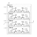
- FIG. 1 is a configuration diagram showing a harmonic mixer 10 according to Embodiment 1;
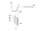
- FIG. FIG. 4 is an explanatory diagram showing respective phases of a first local oscillation wave and a second local oscillation wave; 3 is an explanatory diagram showing respective voltage waveforms in a first local oscillation wave and a second local oscillation wave and waveforms of a current appearing at an output terminal 2;
- FIG. FIG. 4 is an explanatory diagram showing a harmonic mixer in which a switching circuit 11-n has only one first transistor 12-n;
- 2 is an explanatory diagram showing the voltage waveform of the first local oscillation wave applied to the first control terminal 12-nc of the first transistor 12-n and the waveform of the current appearing at the output terminal 2;
- FIG. 3 is a configuration diagram showing a harmonic mixer 10 according to Embodiment 2;
- FIG. 4 is an explanatory diagram showing respective phases of a first local oscillation wave and a second local oscillation wave;
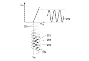
- 3 is an explanatory diagram showing respective voltage waveforms in a first local oscillation wave and a second local oscillation wave and waveforms of a current appearing at an output terminal 2;
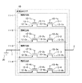
- FIG. FIG. 10 is a configuration diagram showing a harmonic mixer 10 according to Embodiment 3;
- 1 is a configuration diagram showing a control device according to Embodiments 1 to 3;
- FIG. 3 is a hardware configuration diagram of a computer in which a control circuit 30 is implemented by software, firmware, or the like;
- FIG. 1 is a configuration diagram showing a harmonic mixer 10 according to Embodiment 1.
- the harmonic mixer 10 has N switching circuits 11-1 to 11-N. N is an integer of 3 or more.
- the harmonic mixer 10 converts, for example, frequencies in the sub-terahertz band. However, the harmonic mixer 10 is not limited to frequency conversion in the sub-terahertz band, and may perform frequency conversion in other frequency bands.
- the other end of the switching circuit 11-n is connected to the output terminal 2.
- FIG. The N switching circuits 11-1 to 11-N are connected in parallel.
- the four switching circuits 11-1 to 11-4 are connected in parallel.
- An input terminal 1 is a terminal to which a signal is applied.
- the output terminal 2 is a terminal for outputting a signal after frequency conversion by the harmonic mixer 10 .
- the frequency of the signal after frequency conversion is the second frequency, and the second frequency is N times the first frequency fLO .
- the first transistor 12-n has a first terminal 12-na, a second terminal 12-nb and a first control terminal 12-nc. If the first transistor 12-n is for example realized by a FET, the first terminal 12-na is the source terminal of the FET, the second terminal 12-nb is the drain terminal of the FET, the first control Terminal 12-nc is the gate terminal of the FET.
- a first terminal 12-na of the first transistor 12-n is connected to the input terminal 1.
- FIG. A second terminal 12-nb of the first transistor 12-n is connected to a third terminal 13-na of the second transistor 13-n.
- a fourth terminal 13-nb of the second transistor 13-n is connected to the output terminal 2.
- FIG. A first local oscillation wave is applied from the control circuit 30 of the control device shown in FIG. 10 to the first control terminal 12-nc of the first transistor 12-n.
- the frequency of the first local oscillator wave is the first frequency f LO .
- the phase of the first local oscillation wave is ((360/N) ⁇ (n ⁇ 1)+ ⁇ ) degrees. ⁇ is 0 or more and less than 360.
- the first transistor 12-n operates between the first terminal 12-na and the second terminal 12 when the voltage of the first local oscillation wave applied to the first control terminal 12-nc is equal to or higher than the threshold voltage Vth. -nb becomes closed. When the voltage of the first local oscillation wave applied to the first control terminal 12-nc is less than the threshold voltage Vth, the first transistor 12-n operates between the first terminal 12-na and the second terminal 12-na. -nb becomes open.
- the second transistor 13-n has a third terminal 13-na, a fourth terminal 13-nb and a second control terminal 13-nc. If the second transistor 13-n is for example realized by a FET, the third terminal 13-na is the source terminal of the FET, the fourth terminal 13-nb is the drain terminal of the FET, the second control Terminal 13-nc is the gate terminal of the FET.
- a second local oscillation wave is applied from the control circuit 30 of the control device shown in FIG. 10 to the second control terminal 13-nc of the second transistor 13-n.
- the frequency of the second local oscillator wave is the first frequency f LO .
- the phase of the second local oscillation wave is ((360/N) ⁇ n+ ⁇ ) degree.
- the second transistor 13-n connects the third terminal 13-na and the fourth terminal 13 when the voltage of the second local oscillation wave applied to the second control terminal 13-nc is equal to or higher than the threshold voltage Vth. -nb is closed.
- the second transistor 13-n operates between the third terminal 13-na and the fourth terminal 13-na. -nb becomes open.
- FIG. 10 is a configuration diagram showing a control device according to Embodiments 1-3.
- the control device shown in FIG. 10 has a control circuit 30 .
- the control circuit 30 connects the first control terminal 12-nc of the first transistor 12-n included in the n-th switching circuit 11-n among the N switching circuits 11-1 to 11-N.
- the frequency is the first frequency f LO and the phase is ((360/N) ⁇ (n ⁇ 1)+ ⁇ ) degrees.
- the control circuit 30 controls the second control terminal 13-nc of the second transistor 13-n included in the n-th switching circuit 11-n at the first frequency f LO . , giving a second local oscillation wave with a phase of ((360/N) ⁇ n+ ⁇ ) degrees.
- control circuit 30 is implemented by dedicated hardware.
- the control circuit 30 may be realized by software, firmware, or a combination of software and firmware.
- Software or firmware is stored as a program in a computer's memory.
- a computer means hardware that executes a program, for example, a CPU (Central Processing Unit), a central processing unit, a processing unit, an arithmetic unit, a microprocessor, a microcomputer, a processor, or a DSP (Digital Signal Processor). do.
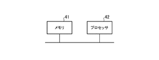
- FIG. 11 is a hardware configuration diagram of a computer when the control circuit 30 is implemented by software, firmware, or the like.
- the memory 41 stores a program for causing a computer to execute the processing procedure of the control circuit 30 .
- the processor 42 of the computer executes the program stored in the memory 41 .
- FIG. 2 is an explanatory diagram showing respective phases of the first local oscillation wave and the second local oscillation wave.
- the frequency of the first local oscillation wave supplied from the control circuit 30 to the first control terminal 12-nc is the first frequency fLO , and the phase of the first local oscillation wave is ((360/N) ⁇ (n ⁇ 1)+ ⁇ ) degrees.
- a first local oscillation wave with a phase of 0 degrees is applied to the first control terminal 12-1c of the first transistor 12-1, and the first transistor 12-2 has A first local oscillation wave having a phase of 90 degrees is applied to the first control terminal 12-2c.
- a first local oscillation wave having a phase of 180 degrees is applied to a first control terminal 12-3c of the first transistor 12-3, and a first control terminal 12-3c of the first transistor 12-4 is applied.
- a first local oscillation wave having a phase of 270 degrees is applied to the terminal 12-4c.
- ⁇ 0.
- the first local oscillation wave applied to the first control terminal 12-1c has a phase difference of 90 degrees from the first local oscillation wave applied to the first control terminal 12-2c. There is a phase difference of 180 degrees from the first local oscillation wave applied to the control terminal 12-3c, and a phase difference of 270 degrees from the first local oscillation wave applied to the first control terminal 12-4c.
- the frequency of the second local oscillation wave supplied from the control circuit 30 to the second control terminal 13-nc is the first frequency fLO , and the phase of the second local oscillation wave is ((360/N) ⁇ n+ ⁇ ) degree.
- a second local oscillation wave having a phase of 90 degrees is applied to the second control terminal 13-1c of the second transistor 13-1, and the second transistor 13-2 has A second local oscillation wave having a phase of 180 degrees is applied to the second control terminal 13-2c.
- a second local oscillation wave having a phase of 270 degrees is applied to a second control terminal 13-3c of the second transistor 13-3, and a second control terminal 13-3c of the second transistor 13-4 is applied.
- FIG. 3 is an explanatory diagram showing respective voltage waveforms in the first local oscillation wave and the second local oscillation wave and the waveform of the current appearing at the output terminal 2.
- a voltage waveform 101 is a voltage waveform of each of the first local oscillation wave with a phase of 0 degree and the second local oscillation wave with a phase of 0 degree.
- a voltage waveform 102 is a voltage waveform of each of the first local oscillation wave with a phase of 90 degrees and the second local oscillation wave with a phase of 90 degrees.
- a voltage waveform 103 is a voltage waveform of each of the first local oscillation wave with a phase of 180 degrees and the second local oscillation wave with a phase of 180 degrees.
- a voltage waveform 104 is a voltage waveform of each of the first local oscillation wave with a phase of 270 degrees and the second local oscillation wave with a phase of 270 degrees.
- Vth is the threshold voltage of each of the first transistor 12-n and the second transistor 13-n.
- the first transistor 12-n operates between the first terminal 12-na and the second terminal when the voltage of the first local oscillation wave applied to the first control terminal 12-nc is equal to or higher than the threshold voltage Vth. 12-nb is closed.
- the first transistor 12-n is in an open state between the first terminal 12-na and the second terminal 12-nb when the voltage of the first local oscillation wave is less than the threshold voltage Vth.
- the second transistor 13-n connects the third terminal 13-na and the fourth terminal 13-nb is closed.
- the second transistor 13-n is in an open state between the third terminal 13-na and the fourth terminal 13-nb when the voltage of the second local oscillation wave is less than the threshold voltage Vth.
- the magnitude of the current flowing through the switching circuit 11-n is the first current that can flow between the first terminal 12-na and the second terminal 12-nb of the first transistor 12-n. , and a second current that can flow between the third terminal 13-na and the fourth terminal 13-nb of the second transistor 13-n. do.
- a composite voltage waveform 105 is a voltage waveform formed by the voltage waveforms 101 to 104 when a current flows through one of the switching circuits 11-1 to 11-4.
- Envelope 106 is the envelope of composite voltage waveform 105 .
- a current waveform 107 is the waveform of the current appearing at the output terminal 2 .
- the composite voltage waveform 105 is converted into a current waveform by the respective V GS -I DS characteristics (transfer characteristics) of the first transistor 12-n and the second transistor 13-n.
- a current waveform 107 is a waveform after conversion according to the V GS -I DS characteristic.
- the waveform of the current flowing through any one of the switching circuits has a waveform similar to the composite voltage waveform 105 . Since the frequency of the composite voltage waveform 105 is 4 ⁇ f LO as shown in FIG. 3, the frequency of the current appearing at the output terminal 2 is also 4 ⁇ f LO . That is, the frequency 4 ⁇ f LO of the current appearing at the output terminal 2 is four times the frequency f LO of each of the first local oscillation wave and the second local oscillation wave.
- FIG. 4 is an explanatory diagram showing a harmonic mixer in which the switching circuit 11-n has only one first transistor 12-n.
- FIG. 5 is an explanatory diagram showing the voltage waveform of the first local oscillation wave applied to the first control terminal 12-nc of the first transistor 12-n and the waveform of the current appearing at the output terminal 2.
- a combined voltage waveform 108 is a voltage waveform formed by the voltage waveforms 101 to 104 when a current flows through one of the switching circuits 11-1 to 11-4, ie, the switching circuit 11-n.
- a current waveform 109 is the waveform of the current appearing at the output terminal 2 .
- the composite voltage waveform 108 is transformed into a current waveform by the respective V GS -I DS characteristics of the first transistor 12-n and the second transistor 13-n.
- a current waveform 109 is a waveform after conversion by the V GS -I DS characteristic.
- the switching circuit 11-n comprises only one first transistor 12-n
- the magnitude of the current flowing through the switching circuit 11-n is determined by the first terminal 12-na of the first transistor 12-n. and the second terminal 12-nb. Since the switching circuit 11-n does not include the second transistor 13-n, the magnitude of the first current is the third terminal 13-na and the fourth terminal 13-n of the second transistor 13-n. nb, the magnitude of the current flowing through the switching circuit 11-n is not limited to the magnitude of the second current.
- the switching circuit 11-n includes the first transistor 12-n and the second transistor 13-n. Current consumption can be reduced more than when only the transistor 12-n is provided.
- the switching circuit 11-n includes only one first transistor 12-n, there occurs a period in which current flows simultaneously through a plurality of switching circuits.
- the switching circuit 11-n Compared to the current waveform 109 when the switching circuit 11-n has only one first transistor 12-n, the switching circuit 11-n has the first transistor 12-n and the second transistor 13-n.
- the current waveform 107 with n has a larger amplitude. Therefore, the harmonic mixer 10 shown in FIG. 1 increases the power of the signal after frequency conversion, as compared with the harmonic mixer in which the switching circuit 11-n includes only one first transistor 12-n. be able to.
- the voltage waveforms 101 to 104 may be distorted due to saturation of the first local oscillation wave and the second local oscillation wave.
- switching circuit 11-n includes first transistor 12-n and second transistor 13-n.
- the composite voltage waveform 105 has a larger amplitude. Therefore, the distortion of the voltage waveforms 101 to 104 has less influence on the composite voltage waveform 105 than the distortion of the voltage waveforms 101 to 104 has on the composite voltage waveform 108 . That is, the harmonic mixer 10 shown in FIG. 1 is less affected by the distortion of the voltage waveforms 101 to 104 than the harmonic mixer in which the switching circuit 11-n includes only one first transistor 12-n. Become.
- the first transistor 12-n having the first terminal 12-na connected to the input terminal 1 to which a signal is applied, the second terminal 12-nb, It has a third terminal 13-na connected to the second terminal 12-nb, and a fourth terminal 13-nb connected to the output terminal 2 for outputting the signal after frequency conversion.
- the first transistor 12-n included in the n-th switching circuit 11-n has a frequency of the first frequency.
- the second transistor 13-n included in the n-th switching circuit 11-n has a frequency of the first frequency and a phase of a second local oscillation wave of ((360/N) ⁇ n+ ⁇ ) degrees. is applied to the second control terminal 13-nc, and only when the voltage of the second local oscillation wave is equal to or higher than the threshold voltage, between the third terminal 13-na and the fourth terminal 13-nb The gap is closed.
- ⁇ is 0 or more and less than 360. Therefore, the harmonic mixer 10 can output a signal having a frequency N times as high as the frequency of the local oscillation wave using transistors.
- FIG. 6 is a configuration diagram showing the harmonic mixer 10 according to the second embodiment.
- the same reference numerals as in FIG. 1 denote the same or corresponding parts, so the description is omitted.
- the frequency of the first local oscillation wave applied from the control circuit 30 to the first control terminal 12-nc is the first frequency f LO .
- the phase of the first local oscillation wave is ((360/N) ⁇ (n ⁇ 1)+ ⁇ ) degrees. 0 or more and less than 360.
- a second local oscillation wave is applied from the control circuit 30 of the control device shown in FIG.
- the frequency of the second local oscillation wave applied from the control circuit 30 to the second control terminal 13-nc is the first frequency f LO .
- the phase of the second local oscillation wave is ((360/N) ⁇ n+ ⁇ ) degrees.
- FIG. 7 is an explanatory diagram showing respective phases of the first local oscillation wave and the second local oscillation wave.
- a first local oscillator wave of 100 degrees is applied.
- a first local oscillation wave with a phase of 0 degrees is applied to the first control terminal 12-1c of the first transistor 12-1, and the first transistor 12-2 has A first local oscillation wave having a phase of 120 degrees is applied to the first control terminal 12-2c.
- a first local oscillation wave having a phase of 240 degrees is applied to the first control terminal 12-3c of the first transistor 12-3.
- ⁇ 0.
- a second control terminal 13-nc of the second transistor 13-n has a phase of ((360/N) ⁇ n+ ⁇ ) degrees from the control circuit 30.
- a local oscillation wave is applied.
- a second local oscillation wave having a phase of 120 degrees is applied to the second control terminal 13-1c of the second transistor 13-1, and the second transistor 13-2 has A second local oscillation wave having a phase of 240 degrees is applied to the second control terminal 13-2c.
- the second local oscillation wave applied to the second control terminal 13-1c has a phase difference of 120 degrees from the second local oscillation wave applied to the second control terminal 13-2c. There is a phase difference of 240 degrees from the second local oscillation wave applied to the control terminal 13-3c.
- FIG. 8 is an explanatory diagram showing respective voltage waveforms of the first local oscillation wave and the second local oscillation wave, and current waveforms appearing at the output terminal 2.
- voltage waveforms 201 are waveforms of respective voltages in the first local oscillation wave with a phase of 0 degree and the second local oscillation wave with a phase of 0 degree.
- a voltage waveform 202 is a voltage waveform of each of the first local oscillation wave with a phase of 120 degrees and the second local oscillation wave with a phase of 120 degrees.
- a voltage waveform 203 is a voltage waveform of each of the first local oscillation wave with a phase of 240 degrees and the second local oscillation wave with a phase of 240 degrees.
- the magnitude of the current flowing through the switching circuit 11-n is the first current that can flow between the first terminal 12-na and the second terminal 12-nb of the first transistor 12-n. , and a second current that can flow between the third terminal 13-na and the fourth terminal 13-nb of the second transistor 13-n. do.
- switching circuit 11-2 when a current flows through the switching circuit 11-2, no current flows through the switching circuits 11-1 and 11-3.
- switching circuit 11-3 When a current flows through the switching circuit 11-3, no current flows through the switching circuits 11-1 and 11-2.
- the switching circuits through which the current flows are switched, for example, in the order of switching circuit 11-1, switching circuit 11-2, and switching circuit 11-3.
- a composite voltage waveform 204 is a voltage waveform formed by the voltage waveforms 201 to 203 when a current flows through one of the switching circuits 11-1 to 11-3, ie, the switching circuit 11-n.
- Envelope 205 is the envelope of composite voltage waveform 204 .
- a current waveform 206 is the waveform of the current appearing at the output terminal 2 .
- the composite voltage waveform 204 is transformed into a current waveform by the respective V GS -I DS characteristics of the first transistor 12-n and the second transistor 13-n.
- a current waveform 206 is a converted waveform according to the V GS -I DS characteristic.
- the switching circuits through which the current flows are switched, for example, in the order of the switching circuit 11-1, the switching circuit 11-2, and the switching circuit 11-3.
- the waveform is similar to Since the frequency of the composite voltage waveform 204 is 3 ⁇ f LO as shown in FIG. 8, the frequency of the current appearing at the output terminal 2 is also 3 ⁇ f LO . That is, the frequency 3 ⁇ f LO of the current appearing at the output terminal 2 is three times the frequency f LO of each of the first local oscillation wave and the second local oscillation wave.
- N may be an integer of 3 or more.
- a signal with LO can be output.
- Embodiment 3 a harmonic mixer 10 in which a ground conductor 20 is connected to an input terminal 1 will be described.
- FIG. 9 is a configuration diagram showing the harmonic mixer 10 according to the third embodiment.
- the same reference numerals as those in FIGS. 1 and 6 denote the same or corresponding parts, so description thereof will be omitted.
- a ground conductor 20 is connected to the input terminal 1 .
- ground conductor 20 is applied to harmonic mixer 10 shown in FIG.
- the harmonic mixer 10 By connecting the ground conductor 20 to the input terminal 1, the harmonic mixer 10 generates a frequency N ⁇ f LO that is N times the frequency f LO of each of the first local oscillation wave and the second local oscillation wave. can be used as a multiplier capable of outputting a signal having
- the present disclosure is suitable for harmonic mixers and controllers.
Landscapes
- Engineering & Computer Science (AREA)
- Power Engineering (AREA)
- Superheterodyne Receivers (AREA)
- Transmitters (AREA)
Abstract
信号が与えられる入力端子(1)と接続される第1の端子(12-na)と、第2の端子(12-nb)とを有している第1のトランジスタ(12-n)と、第2の端子(12-nb)と接続されている第3の端子(13-na)と、周波数変換後の信号を出力するための出力端子(2)と接続される第4の端子(13-nb)とを有している第2のトランジスタ(13-n)とを備える開閉回路(11-n)がN個並列に接続されているように、高調波ミクサ(10)を構成した。n=1,・・・,Nである。高調波ミクサ(10)が備えるN個の開閉回路(11-1)~(11-N)のうち、n番目の開閉回路(11-n)に含まれている第1のトランジスタ(12-n)は、周波数が第1の周波数であり、位相が((360/N)×(n-1)+θ)度の第1の局部発振波が与えられる第1の制御端子(12-nc)を有し、第1の局部発振波の電圧が閾値電圧以上であるときに限り、第1の端子(12-na)と第2の端子(12-nb)との間が閉状態になる。n番目の開閉回路(11-n)に含まれている第2のトランジスタ(13-n)は、周波数が第1の周波数であり、位相が((360/N)×n+θ)度の第2の局部発振波が与えられる第2の制御端子(13-nc)を有し、第2の局部発振波の電圧が閾値電圧以上であるときに限り、第3の端子(13-na)と第4の端子(13-nb)との間が閉状態になるものである。θは、0以上360未満である。
Description
本開示は、高調波ミクサ及び制御装置に関するものである。
低損失な周波数変換を実現するために、トランジスタを用いて周波数を変換する高調波ミクサが非特許文献1に開示されている。当該高調波ミクサは、2つのトランジスタを備えている。2つのトランジスタのうち、一方のトランジスタのドレイン端子は、他方のトランジスタのドレイン端子と接続されている。また、一方のトランジスタのソース端子は、他方のトランジスタのソース端子と接続されている。
一方のトランジスタのゲート端子には、第1の局部発振波が与えられる。他方のトランジスタのゲート端子には、第1の局部発振波よりも、位相が180度遅れている第2の局部発振波が与えられる。第1の局部発振波の周波数と第2の局部発振波の周波数とは、同一の周波数fLOである。2つのトランジスタのソース端子に信号が与えられたとき、それぞれのトランジスタのドレイン端子が接続されている出力端子から、周波数fLOの2倍の周波数2×fLOを有する信号が出力される。
一方のトランジスタのゲート端子には、第1の局部発振波が与えられる。他方のトランジスタのゲート端子には、第1の局部発振波よりも、位相が180度遅れている第2の局部発振波が与えられる。第1の局部発振波の周波数と第2の局部発振波の周波数とは、同一の周波数fLOである。2つのトランジスタのソース端子に信号が与えられたとき、それぞれのトランジスタのドレイン端子が接続されている出力端子から、周波数fLOの2倍の周波数2×fLOを有する信号が出力される。
"A 300GHz Wireless Transceiver in 65nm CMOS for IEEE802.15.3d Using Push-Push Subharmonic Mixer",2020 IEEE/MTT-S International Microwave Symposium
非特許文献1に開示されている高調波ミクサは、局部発振波の周波数fLOのN(Nは、3以上の整数)倍の周波数N×fLOを有する信号を出力することができないという課題があった。
本開示は、上記のような課題を解決するためになされたもので、トランジスタを用いて、局部発振波が有する周波数のN倍の周波数を有する信号を出力することができる高調波ミクサを得ることを目的とする。
本開示に係る高調波ミクサは、信号が与えられる入力端子と接続される第1の端子と、第2の端子とを有する第1のトランジスタと、第2の端子と接続されている第3の端子と、第1の周波数のN(Nは、3以上の整数)倍の周波数を有する信号を出力するための出力端子と接続される第4の端子とを有する第2のトランジスタとを備える開閉回路がN個並列に接続されている。当該高調波ミクサが備えるN個の開閉回路のうち、n(n=1,・・・,N)番目の開閉回路に含まれている第1のトランジスタは、周波数が第1の周波数であり、位相が((360/N)×(n-1)+θ(θは、0以上360未満))度の第1の局部発振波が与えられる第1の制御端子を有し、第1の局部発振波の電圧が閾値電圧以上であるときに限り、第1の端子と第2の端子との間が閉状態になり、n番目の開閉回路に含まれている第2のトランジスタは、周波数が第1の周波数であり、位相が((360/N)×n+θ)度の第2の局部発振波が与えられる第2の制御端子を有し、第2の局部発振波の電圧が閾値電圧以上であるときに限り、第3の端子と第4の端子との間が閉状態になるものである。
本開示によれば、トランジスタを用いて、局部発振波が有する周波数のN倍の周波数を有する信号を出力することができる。
以下、本開示をより詳細に説明するために、本開示を実施するための形態について、添付の図面に従って説明する。
実施の形態1.
図1は、実施の形態1に係る高調波ミクサ10を示す構成図である。
高調波ミクサ10は、N個の開閉回路11-1~11-Nを備えている。Nは、3以上の整数である。高調波ミクサ10は、例えば、サブテラヘルツ帯の周波数を変換するものである。ただし、高調波ミクサ10は、サブテラヘルツ帯の周波数変換に限るものではなく、他の周波数帯の周波数変換を行うものであってもよい。
図1は、実施の形態1に係る高調波ミクサ10を示す構成図である。
高調波ミクサ10は、N個の開閉回路11-1~11-Nを備えている。Nは、3以上の整数である。高調波ミクサ10は、例えば、サブテラヘルツ帯の周波数を変換するものである。ただし、高調波ミクサ10は、サブテラヘルツ帯の周波数変換に限るものではなく、他の周波数帯の周波数変換を行うものであってもよい。
N個の開閉回路11-1~11-Nのうち、n(n=1,・・・,N)番目の開閉回路11-nの一端は、入力端子1と接続される。開閉回路11-nの他端は、出力端子2と接続される。N個の開閉回路11-1~11-Nは、並列に接続されている。
図1に示す高調波ミクサ10では、N=4の例を示しており、高調波ミクサ10が4個の開閉回路11-1~11-4を備えている。4個の開閉回路11-1~11-4は、並列に接続されている。
図1に示す高調波ミクサ10では、N=4の例を示しており、高調波ミクサ10が4個の開閉回路11-1~11-4を備えている。4個の開閉回路11-1~11-4は、並列に接続されている。
入力端子1は、信号が与えられる端子である。
出力端子2は、高調波ミクサ10による周波数変換後の信号を出力するための端子である。周波数変換後の信号が有する周波数は、第2の周波数であり、第2の周波数は、第1の周波数fLOのN倍である。
出力端子2は、高調波ミクサ10による周波数変換後の信号を出力するための端子である。周波数変換後の信号が有する周波数は、第2の周波数であり、第2の周波数は、第1の周波数fLOのN倍である。
開閉回路11-n(n=1,・・・,N)は、第1のトランジスタ12-nと、第2のトランジスタ13-nとを備えている。
第1のトランジスタ12-n(n=1,・・・,N)は、MOS(Metal Oxide Semiconductor )トランジスタ、バイポーラトランジスタ、又は、FET(Field Effect Transistor)等によって実現される。
第1のトランジスタ12-nは、第1の端子12-na、第2の端子12-nb及び第1の制御端子12-ncを有している。
第1のトランジスタ12-nが、例えば、FETによって実現される場合、第1の端子12-naは、FETのソース端子、第2の端子12-nbは、FETのドレイン端子、第1の制御端子12-ncは、FETのゲート端子である。
第1のトランジスタ12-nは、第1の端子12-na、第2の端子12-nb及び第1の制御端子12-ncを有している。
第1のトランジスタ12-nが、例えば、FETによって実現される場合、第1の端子12-naは、FETのソース端子、第2の端子12-nbは、FETのドレイン端子、第1の制御端子12-ncは、FETのゲート端子である。
第1のトランジスタ12-nが有する第1の端子12-naは、入力端子1と接続される。
第1のトランジスタ12-nが有する第2の端子12-nbは、第2のトランジスタ13-nが有する第3の端子13-naと接続されている。
第2のトランジスタ13-nが有する第4の端子13-nbは、出力端子2と接続される。
第1のトランジスタ12-nが有する第1の制御端子12-ncには、図10に示す制御装置の制御回路30から第1の局部発振波が与えられる。第1の局部発振波の周波数は、第1の周波数fLOである。第1の局部発振波の位相は、((360/N)×(n-1)+θ)度である。θは、0以上360未満である。
第1のトランジスタ12-nが有する第2の端子12-nbは、第2のトランジスタ13-nが有する第3の端子13-naと接続されている。
第2のトランジスタ13-nが有する第4の端子13-nbは、出力端子2と接続される。
第1のトランジスタ12-nが有する第1の制御端子12-ncには、図10に示す制御装置の制御回路30から第1の局部発振波が与えられる。第1の局部発振波の周波数は、第1の周波数fLOである。第1の局部発振波の位相は、((360/N)×(n-1)+θ)度である。θは、0以上360未満である。
第1のトランジスタ12-nは、第1の制御端子12-ncに与えられる第1の局部発振波の電圧が閾値電圧Vth以上であるとき、第1の端子12-naと第2の端子12-nbとの間が閉状態になる。
第1のトランジスタ12-nは、第1の制御端子12-ncに与えられる第1の局部発振波の電圧が閾値電圧Vth未満であるとき、第1の端子12-naと第2の端子12-nbとの間が開状態になる。
第1のトランジスタ12-nは、第1の制御端子12-ncに与えられる第1の局部発振波の電圧が閾値電圧Vth未満であるとき、第1の端子12-naと第2の端子12-nbとの間が開状態になる。
第2のトランジスタ13-n(n=1,・・・,N)は、MOSトランジスタ、バイポーラトランジスタ、又は、FET等によって実現される。
第2のトランジスタ13-nは、第3の端子13-na、第4の端子13-nb及び第2の制御端子13-ncを有している。
第2のトランジスタ13-nが、例えば、FETによって実現される場合、第3の端子13-naは、FETのソース端子、第4の端子13-nbは、FETのドレイン端子、第2の制御端子13-ncは、FETのゲート端子である。
第2のトランジスタ13-nは、第3の端子13-na、第4の端子13-nb及び第2の制御端子13-ncを有している。
第2のトランジスタ13-nが、例えば、FETによって実現される場合、第3の端子13-naは、FETのソース端子、第4の端子13-nbは、FETのドレイン端子、第2の制御端子13-ncは、FETのゲート端子である。
第2のトランジスタ13-nが有する第2の制御端子13-ncには、図10に示す制御装置の制御回路30から第2の局部発振波が与えられる。第2の局部発振波の周波数は、第1の周波数fLOである。第2の局部発振波の位相は、((360/N)×n+θ)
度である。
第2のトランジスタ13-nは、第2の制御端子13-ncに与えられる第2の局部発振波の電圧が閾値電圧Vth以上であるとき、第3の端子13-naと第4の端子13-nbとの間が閉状態になる。
第2のトランジスタ13-nは、第2の制御端子13-ncに与えられる第2の局部発振波の電圧が閾値電圧Vth未満であるとき、第3の端子13-naと第4の端子13-nbとの間が開状態になる。
度である。
第2のトランジスタ13-nは、第2の制御端子13-ncに与えられる第2の局部発振波の電圧が閾値電圧Vth以上であるとき、第3の端子13-naと第4の端子13-nbとの間が閉状態になる。
第2のトランジスタ13-nは、第2の制御端子13-ncに与えられる第2の局部発振波の電圧が閾値電圧Vth未満であるとき、第3の端子13-naと第4の端子13-nbとの間が開状態になる。
図10は、実施の形態1~3に係る制御装置を示す構成図である。
図10に示す制御装置は、制御回路30を備えている。
制御回路30は、N個の開閉回路11-1~11-Nのうち、n番目の開閉回路11-nに含まれている第1のトランジスタ12-nが有する第1の制御端子12-ncに対して、周波数が第1の周波数fLOであり、位相が((360/N)×(n-1)+θ)度の第1の局部発振波を与える。
また、制御回路30は、n番目の開閉回路11-nに含まれている第2のトランジスタ13-nが有する第2の制御端子13-ncに対して、周波数が第1の周波数fLOであり、位相が((360/N)×n+θ)度の第2の局部発振波を与える。
図10に示す制御装置は、制御回路30を備えている。
制御回路30は、N個の開閉回路11-1~11-Nのうち、n番目の開閉回路11-nに含まれている第1のトランジスタ12-nが有する第1の制御端子12-ncに対して、周波数が第1の周波数fLOであり、位相が((360/N)×(n-1)+θ)度の第1の局部発振波を与える。
また、制御回路30は、n番目の開閉回路11-nに含まれている第2のトランジスタ13-nが有する第2の制御端子13-ncに対して、周波数が第1の周波数fLOであり、位相が((360/N)×n+θ)度の第2の局部発振波を与える。
図10に示す制御装置では、制御回路30が専用のハードウェアによって実現されるものを想定している。しかし、制御回路30は、ソフトウェア、ファームウェア、又は、ソフトウェアとファームウェアとの組み合わせによって実現されるものであってもよい。
ソフトウェア又はファームウェアは、プログラムとして、コンピュータのメモリに格納される。コンピュータは、プログラムを実行するハードウェアを意味し、例えば、CPU(Central Processing Unit)、中央処理装置、処理装置、演算装置、マイクロプロセッサ、マイクロコンピュータ、プロセッサ、あるいは、DSP(Digital Signal Processor)が該当する。
ソフトウェア又はファームウェアは、プログラムとして、コンピュータのメモリに格納される。コンピュータは、プログラムを実行するハードウェアを意味し、例えば、CPU(Central Processing Unit)、中央処理装置、処理装置、演算装置、マイクロプロセッサ、マイクロコンピュータ、プロセッサ、あるいは、DSP(Digital Signal Processor)が該当する。
図11は、制御回路30が、ソフトウェア又はファームウェア等によって実現される場合のコンピュータのハードウェア構成図である。
制御回路30が、ソフトウェア又はファームウェア等によって実現される場合、制御回路30の処理手順をコンピュータに実行させるためのプログラムがメモリ41に格納される。そして、コンピュータのプロセッサ42がメモリ41に格納されているプログラムを実行する。
制御回路30が、ソフトウェア又はファームウェア等によって実現される場合、制御回路30の処理手順をコンピュータに実行させるためのプログラムがメモリ41に格納される。そして、コンピュータのプロセッサ42がメモリ41に格納されているプログラムを実行する。
次に、図1に示す高調波ミクサ10について説明する。
図2は、第1の局部発振波及び第2の局部発振波におけるそれぞれの位相を示す説明図である。
第1のトランジスタ12-n(n=1,・・・,4)が有する第1の制御端子12-ncには、図10に示す制御装置の制御回路30から、第1の局部発振波が与えられる。制御回路30から第1の制御端子12-ncに与えられる第1の局部発振波の周波数は、第1の周波数fLOであり、第1の局部発振波の位相は、((360/N)×(n-1)+θ)度である。
図2は、第1の局部発振波及び第2の局部発振波におけるそれぞれの位相を示す説明図である。
第1のトランジスタ12-n(n=1,・・・,4)が有する第1の制御端子12-ncには、図10に示す制御装置の制御回路30から、第1の局部発振波が与えられる。制御回路30から第1の制御端子12-ncに与えられる第1の局部発振波の周波数は、第1の周波数fLOであり、第1の局部発振波の位相は、((360/N)×(n-1)+θ)度である。
図2の例では、第1のトランジスタ12-1が有する第1の制御端子12-1cには、位相が0度の第1の局部発振波が与えられ、第1のトランジスタ12-2が有する第1の制御端子12-2cには、位相が90度の第1の局部発振波が与えられる。
また、第1のトランジスタ12-3が有する第1の制御端子12-3cには、位相が180度の第1の局部発振波が与えられ、第1のトランジスタ12-4が有する第1の制御端子12-4cには、位相が270度の第1の局部発振波が与えられる。図2の例では、θ=0である。θは、0以上360未満であればよく、θ=0に限るものではない。
したがって、第1の制御端子12-1cに与えられる第1の局部発振波は、第1の制御端子12-2cに与えられる第1の局部発振波と90度の位相差があり、第1の制御端子12-3cに与えられる第1の局部発振波と180度の位相差があり、第1の制御端子12-4cに与えられる第1の局部発振波と270度の位相差がある。
また、第1のトランジスタ12-3が有する第1の制御端子12-3cには、位相が180度の第1の局部発振波が与えられ、第1のトランジスタ12-4が有する第1の制御端子12-4cには、位相が270度の第1の局部発振波が与えられる。図2の例では、θ=0である。θは、0以上360未満であればよく、θ=0に限るものではない。
したがって、第1の制御端子12-1cに与えられる第1の局部発振波は、第1の制御端子12-2cに与えられる第1の局部発振波と90度の位相差があり、第1の制御端子12-3cに与えられる第1の局部発振波と180度の位相差があり、第1の制御端子12-4cに与えられる第1の局部発振波と270度の位相差がある。
第2のトランジスタ13-n(n=1,・・・,4)が有する第2の制御端子13-ncには、図10に示す制御装置の制御回路30から、第2の局部発振波が与えられる。制御回路30から第2の制御端子13-ncに与えられる第2の局部発振波の周波数は、第1の周波数fLOであり、第2の局部発振波の位相は、((360/N)×n+θ)度である。
図2の例では、第2のトランジスタ13-1が有する第2の制御端子13-1cには、位相が90度の第2の局部発振波が与えられ、第2のトランジスタ13-2が有する第2の制御端子13-2cには、位相が180度の第2の局部発振波が与えられる。
また、第2のトランジスタ13-3が有する第2の制御端子13-3cには、位相が270度の第2の局部発振波が与えられ、第2のトランジスタ13-4が有する第2の制御端子13-4cには、位相が0(=360)度の第2の局部発振波が与えられる。
したがって、第2の制御端子13-1cに与えられる第2の局部発振波は、第2の制御端子13-2cに与えられる第2の局部発振波と90度の位相差があり、第2の制御端子13-3cに与えられる第2の局部発振波と180度の位相差があり、第2の制御端子13-4cに与えられる第2の局部発振波と270度の位相差がある。
また、第2のトランジスタ13-3が有する第2の制御端子13-3cには、位相が270度の第2の局部発振波が与えられ、第2のトランジスタ13-4が有する第2の制御端子13-4cには、位相が0(=360)度の第2の局部発振波が与えられる。
したがって、第2の制御端子13-1cに与えられる第2の局部発振波は、第2の制御端子13-2cに与えられる第2の局部発振波と90度の位相差があり、第2の制御端子13-3cに与えられる第2の局部発振波と180度の位相差があり、第2の制御端子13-4cに与えられる第2の局部発振波と270度の位相差がある。
図3は、第1の局部発振波及び第2の局部発振波におけるそれぞれの電圧波形と出力端子2に現れる電流の波形とを示す説明図である。
図3において、電圧波形101は、位相が0度の第1の局部発振波及び位相が0度の第2の局部発振波におけるそれぞれの電圧の波形である。
電圧波形102は、位相が90度の第1の局部発振波及び位相が90度の第2の局部発振波におけるそれぞれの電圧の波形である。
電圧波形103は、位相が180度の第1の局部発振波及び位相が180度の第2の局部発振波におけるそれぞれの電圧の波形である。
電圧波形104は、位相が270度の第1の局部発振波及び位相が270度の第2の局部発振波におけるそれぞれの電圧の波形である。
図3において、電圧波形101は、位相が0度の第1の局部発振波及び位相が0度の第2の局部発振波におけるそれぞれの電圧の波形である。
電圧波形102は、位相が90度の第1の局部発振波及び位相が90度の第2の局部発振波におけるそれぞれの電圧の波形である。
電圧波形103は、位相が180度の第1の局部発振波及び位相が180度の第2の局部発振波におけるそれぞれの電圧の波形である。
電圧波形104は、位相が270度の第1の局部発振波及び位相が270度の第2の局部発振波におけるそれぞれの電圧の波形である。
Vthは、第1のトランジスタ12-n及び第2のトランジスタ13-nにおけるそれぞれの閾値電圧である。
第1のトランジスタ12-nは、第1の制御端子12-ncに与えられた第1の局部発振波の電圧が閾値電圧Vth以上であるとき、第1の端子12-naと第2の端子12-nbとの間が閉状態となる。第1のトランジスタ12-nは、第1の局部発振波の電圧が閾値電圧Vth未満であるとき、第1の端子12-naと第2の端子12-nbとの間が開状態となる。
第2のトランジスタ13-nは、第2の制御端子13-ncに与えられた第2の局部発振波の電圧が閾値電圧Vth以上であるとき、第3の端子13-naと第4の端子13-nbとの間が閉状態となる。第2のトランジスタ13-nは、第2の局部発振波の電圧が閾値電圧Vth未満であるとき、第3の端子13-naと第4の端子13-nbとの間が開状態となる。
第1のトランジスタ12-nは、第1の制御端子12-ncに与えられた第1の局部発振波の電圧が閾値電圧Vth以上であるとき、第1の端子12-naと第2の端子12-nbとの間が閉状態となる。第1のトランジスタ12-nは、第1の局部発振波の電圧が閾値電圧Vth未満であるとき、第1の端子12-naと第2の端子12-nbとの間が開状態となる。
第2のトランジスタ13-nは、第2の制御端子13-ncに与えられた第2の局部発振波の電圧が閾値電圧Vth以上であるとき、第3の端子13-naと第4の端子13-nbとの間が閉状態となる。第2のトランジスタ13-nは、第2の局部発振波の電圧が閾値電圧Vth未満であるとき、第3の端子13-naと第4の端子13-nbとの間が開状態となる。
入力端子1に信号が与えられているときに、以下の条件(1)(2)を満足するときに、開閉回路11-n(n=1,・・・,4)に電流が流れる。
条件
(1)第1のトランジスタ12-nが有する第1の制御端子12-ncに与えられている第1の局部発振波の電圧が閾値電圧Vth以上である。
(2)第2のトランジスタ13-nが有する第2の制御端子13-ncに与えられている第2の局部発振波の電圧が閾値電圧Vth以上である。
条件
(1)第1のトランジスタ12-nが有する第1の制御端子12-ncに与えられている第1の局部発振波の電圧が閾値電圧Vth以上である。
(2)第2のトランジスタ13-nが有する第2の制御端子13-ncに与えられている第2の局部発振波の電圧が閾値電圧Vth以上である。
開閉回路11-nを流れる電流の大きさは、第1のトランジスタ12-nにおける第1の端子12-naと第2の端子12-nbとの間を流れることが可能な第1の電流と、第2のトランジスタ13-nにおける第3の端子13-naと第4の端子13-nbとの間を流れることが可能な第2の電流とのうち、小さい方の電流の大きさに相当する。
開閉回路11-1に電流が流れるときは、開閉回路11-n(n=2,3,4)における第1の制御端子12-ncに与えられている第1の局部発振波の電圧及び第2の制御端子13-ncに与えられている第2の局部発振波の電圧のうち、少なくとも1つの電圧が閾値電圧Vth未満である。このため、開閉回路11-1に電流が流れるときは、開閉回路11-n(n=2,3,4)には電流が流れない。
開閉回路11-1に電流が流れるときは、開閉回路11-n(n=2,3,4)における第1の制御端子12-ncに与えられている第1の局部発振波の電圧及び第2の制御端子13-ncに与えられている第2の局部発振波の電圧のうち、少なくとも1つの電圧が閾値電圧Vth未満である。このため、開閉回路11-1に電流が流れるときは、開閉回路11-n(n=2,3,4)には電流が流れない。
同様に、開閉回路11-2に電流が流れるときは、開閉回路11-1,11-3,11-4には電流が流れない。開閉回路11-3に電流が流れるときは、開閉回路11-1,11-2,11-4には電流が流れない。開閉回路11-4に電流が流れるときは、開閉回路11-1~11-3には電流が流れない。
電流が流れる開閉回路は、例えば、開閉回路11-1、開閉回路11-2、開閉回路11-3、開閉回路11-4の順番で切り替わる。
電流が流れる開閉回路は、例えば、開閉回路11-1、開閉回路11-2、開閉回路11-3、開閉回路11-4の順番で切り替わる。
合成電圧波形105は、開閉回路11-1~11-4のうちのいずれかの開閉回路11-nに電流が流れるときに、電圧波形101~104によって形成される電圧波形である。
包絡線106は、合成電圧波形105の包絡線である。
電流波形107は、出力端子2に現れる電流の波形である。
合成電圧波形105は、第1のトランジスタ12-n及び第2のトランジスタ13-nにおけるそれぞれのVGS-IDS特性(伝達特性)によって、電流の波形に変換される。電流波形107は、VGS-IDS特性による変換後の波形である。
包絡線106は、合成電圧波形105の包絡線である。
電流波形107は、出力端子2に現れる電流の波形である。
合成電圧波形105は、第1のトランジスタ12-n及び第2のトランジスタ13-nにおけるそれぞれのVGS-IDS特性(伝達特性)によって、電流の波形に変換される。電流波形107は、VGS-IDS特性による変換後の波形である。
電流が流れる開閉回路が、例えば、開閉回路11-1、開閉回路11-2、開閉回路11-3、開閉回路11-4の順番で切り替わることで、いずれか1つの開閉回路に流れる電流の波形は、合成電圧波形105と同様の波形となる。
合成電圧波形105の周波数は、図3に示すように、周波数4×fLOであるため、出力端子2に現れる電流の周波数についても、4×fLOとなる。即ち、出力端子2に現れる電流の周波数4×fLOは、第1の局部発振波及び第2の局部発振波のそれぞれが有する周波数fLOの4倍になっている。
合成電圧波形105の周波数は、図3に示すように、周波数4×fLOであるため、出力端子2に現れる電流の周波数についても、4×fLOとなる。即ち、出力端子2に現れる電流の周波数4×fLOは、第1の局部発振波及び第2の局部発振波のそれぞれが有する周波数fLOの4倍になっている。
図1に示す高調波ミクサ10では、開閉回路11-n(n=1,・・・,4)が、第1のトランジスタ12-nと第2のトランジスタ13-nとを備えている。
図4に示すように、開閉回路11-nが、1つの第1のトランジスタ12-nのみを備えるものであっても、出力端子2に現れる電流の周波数を4×fLOにすることができる。
図4は、開閉回路11-nが1つの第1のトランジスタ12-nのみを備えている高調波ミクサを示す説明図である。
図5は、第1のトランジスタ12-nが有する第1の制御端子12-ncに与えられる第1の局部発振波の電圧波形と出力端子2に現れる電流の波形とを示す説明図である。
合成電圧波形108は、開閉回路11-1~11-4のうちのいずれかの開閉回路11-nに電流が流れるときに、電圧波形101~104によって形成される電圧波形である。
電流波形109は、出力端子2に現れる電流の波形である。
合成電圧波形108は、第1のトランジスタ12-n及び第2のトランジスタ13-nにおけるそれぞれのVGS-IDS特性によって、電流の波形に変換される。電流波形109は、VGS-IDS特性による変換後の波形である。
図4に示すように、開閉回路11-nが、1つの第1のトランジスタ12-nのみを備えるものであっても、出力端子2に現れる電流の周波数を4×fLOにすることができる。
図4は、開閉回路11-nが1つの第1のトランジスタ12-nのみを備えている高調波ミクサを示す説明図である。
図5は、第1のトランジスタ12-nが有する第1の制御端子12-ncに与えられる第1の局部発振波の電圧波形と出力端子2に現れる電流の波形とを示す説明図である。
合成電圧波形108は、開閉回路11-1~11-4のうちのいずれかの開閉回路11-nに電流が流れるときに、電圧波形101~104によって形成される電圧波形である。
電流波形109は、出力端子2に現れる電流の波形である。
合成電圧波形108は、第1のトランジスタ12-n及び第2のトランジスタ13-nにおけるそれぞれのVGS-IDS特性によって、電流の波形に変換される。電流波形109は、VGS-IDS特性による変換後の波形である。
開閉回路11-nが1つの第1のトランジスタ12-nのみを備えている場合、開閉回路11-nを流れる電流の大きさは、第1のトランジスタ12-nにおける第1の端子12-naと第2の端子12-nbとの間を流れる第1の電流の大きさに相当する。開閉回路11-nが第2のトランジスタ13-nを備えていないため、第1の電流の大きさが、第2のトランジスタ13-nにおける第3の端子13-naと第4の端子13-nbとの間を流れることが可能な第2の電流よりも大きい期間であっても、開閉回路11-nを流れる電流の大きさが、第2の電流の大きさに制限されることがない。
図1に示す高調波ミクサ10では、開閉回路11-nが、第1のトランジスタ12-nと第2のトランジスタ13-nとを備えているため、開閉回路11-nが1つの第1のトランジスタ12-nのみを備えている場合よりも、消費電流を低減することができる。
図1に示す高調波ミクサ10では、開閉回路11-nが、第1のトランジスタ12-nと第2のトランジスタ13-nとを備えているため、開閉回路11-nが1つの第1のトランジスタ12-nのみを備えている場合よりも、消費電流を低減することができる。
開閉回路11-nが1つの第1のトランジスタ12-nのみを備えている場合、複数の開閉回路に電流が同時に流れる期間が発生する。
図1に示す高調波ミクサ10では、開閉回路11-1~11-4のうち、いずれか1つの開閉回路11-nのみに電流が流れるため、電流の直流成分を削減でき、低消費電力化を図ることができる。
図1に示す高調波ミクサ10では、開閉回路11-1~11-4のうち、いずれか1つの開閉回路11-nのみに電流が流れるため、電流の直流成分を削減でき、低消費電力化を図ることができる。
開閉回路11-nが1つの第1のトランジスタ12-nのみを備えている場合の電流波形109と比べて、開閉回路11-nが、第1のトランジスタ12-nと第2のトランジスタ13-nとを備えている場合の電流波形107の方が、振幅が大きくなる。したがって、開閉回路11-nが1つの第1のトランジスタ12-nのみを備えている高調波ミクサよりも、図1に示す高調波ミクサ10の方が、周波数変換後の信号の電力を大きくすることができる。
また、第1の局部発振波及び第2の局部発振波のそれぞれが飽和することによって、電圧波形101~104が歪むことがある。
開閉回路11-nが1つの第1のトランジスタ12-nのみを備えている場合の合成電圧波形108と比べて、開閉回路11-nが、第1のトランジスタ12-nと第2のトランジスタ13-nとを備えている場合の合成電圧波形105の方が、振幅が大きくなる。したがって、電圧波形101~104の歪みが合成電圧波形108に与える影響よりも、電圧波形101~104の歪みが合成電圧波形105に与える影響の方が小さくなる。即ち、図1に示す高調波ミクサ10は、開閉回路11-nが1つの第1のトランジスタ12-nのみを備えている高調波ミクサよりも、電圧波形101~104の歪みに伴う影響が小さくなる。
開閉回路11-nが1つの第1のトランジスタ12-nのみを備えている場合の合成電圧波形108と比べて、開閉回路11-nが、第1のトランジスタ12-nと第2のトランジスタ13-nとを備えている場合の合成電圧波形105の方が、振幅が大きくなる。したがって、電圧波形101~104の歪みが合成電圧波形108に与える影響よりも、電圧波形101~104の歪みが合成電圧波形105に与える影響の方が小さくなる。即ち、図1に示す高調波ミクサ10は、開閉回路11-nが1つの第1のトランジスタ12-nのみを備えている高調波ミクサよりも、電圧波形101~104の歪みに伴う影響が小さくなる。
以上の実施の形態1では、信号が与えられる入力端子1と接続される第1の端子12-naと、第2の端子12-nbとを有している第1のトランジスタ12-nと、第2の端子12-nbと接続されている第3の端子13-naと、周波数変換後の信号を出力するための出力端子2と接続される第4の端子13-nbとを有している第2のトランジスタ13-nとを備える開閉回路11-nがN個並列に接続されているように、高調波ミクサ10を構成した。n=1,・・・,Nである。
高調波ミクサ10が備えるN個の開閉回路11-1~11-Nのうち、n番目の開閉回路11-nに含まれている第1のトランジスタ12-nは、周波数が第1の周波数であり、位相が((360/N)×(n-1)+θ)度の第1の局部発振波が与えられる第1の制御端子12-ncを有し、第1の局部発振波の電圧が閾値電圧以上であるときに限り、第1の端子12-naと第2の端子12-nbとの間が閉状態になる。n番目の開閉回路11-nに含まれている第2のトランジスタ13-nは、周波数が第1の周波数であり、位相が((360/N)×n+θ)度の第2の局部発振波が与えられる第2の制御端子13-ncを有し、第2の局部発振波の電圧が閾値電圧以上であるときに限り、第3の端子13-naと第4の端子13-nbとの間が閉状態になるものである。θは、0以上360未満である。
したがって、高調波ミクサ10は、トランジスタを用いて、局部発振波が有する周波数のN倍の周波数を有する信号を出力することができる。
高調波ミクサ10が備えるN個の開閉回路11-1~11-Nのうち、n番目の開閉回路11-nに含まれている第1のトランジスタ12-nは、周波数が第1の周波数であり、位相が((360/N)×(n-1)+θ)度の第1の局部発振波が与えられる第1の制御端子12-ncを有し、第1の局部発振波の電圧が閾値電圧以上であるときに限り、第1の端子12-naと第2の端子12-nbとの間が閉状態になる。n番目の開閉回路11-nに含まれている第2のトランジスタ13-nは、周波数が第1の周波数であり、位相が((360/N)×n+θ)度の第2の局部発振波が与えられる第2の制御端子13-ncを有し、第2の局部発振波の電圧が閾値電圧以上であるときに限り、第3の端子13-naと第4の端子13-nbとの間が閉状態になるものである。θは、0以上360未満である。
したがって、高調波ミクサ10は、トランジスタを用いて、局部発振波が有する周波数のN倍の周波数を有する信号を出力することができる。
実施の形態2.
実施の形態2では、N=3個の開閉回路11-1~11-3が並列に接続されている高調波ミクサ10について説明する。
実施の形態2では、N=3個の開閉回路11-1~11-3が並列に接続されている高調波ミクサ10について説明する。
図6は、実施の形態2に係る高調波ミクサ10を示す構成図である。図6において、図1と同一符号は同一又は相当部分を示すので説明を省略する。
第1のトランジスタ12-n(n=1,2,3)が有する第1の制御端子12-ncには、図10に示す制御装置の制御回路30から第1の局部発振波が与えられる。制御回路30から第1の制御端子12-ncに与えられる第1の局部発振波の周波数は、第1の周波数fLOである。第1の局部発振波の位相は、((360/N)×(n-1)+θ)度である。0以上360未満である。
第2のトランジスタ13-nが有する第2の制御端子13-ncには、図10に示す制御装置の制御回路30から第2の局部発振波が与えられる。制御回路30から第2の制御端子13-ncに与えられる第2の局部発振波の周波数は、第1の周波数fLOである。第2の局部発振波の位相は、((360/N)×n+θ)度である。
第1のトランジスタ12-n(n=1,2,3)が有する第1の制御端子12-ncには、図10に示す制御装置の制御回路30から第1の局部発振波が与えられる。制御回路30から第1の制御端子12-ncに与えられる第1の局部発振波の周波数は、第1の周波数fLOである。第1の局部発振波の位相は、((360/N)×(n-1)+θ)度である。0以上360未満である。
第2のトランジスタ13-nが有する第2の制御端子13-ncには、図10に示す制御装置の制御回路30から第2の局部発振波が与えられる。制御回路30から第2の制御端子13-ncに与えられる第2の局部発振波の周波数は、第1の周波数fLOである。第2の局部発振波の位相は、((360/N)×n+θ)度である。
次に、図6に示す高調波ミクサ10について説明する。
図7は、第1の局部発振波及び第2の局部発振波におけるそれぞれの位相を示す説明図である。
第1のトランジスタ12-n(n=1,2,3)が有する第1の制御端子12-ncには、制御回路30から、位相が((360/N)×(n-1)+θ)度の第1の局部発振波が与えられる。
図7は、第1の局部発振波及び第2の局部発振波におけるそれぞれの位相を示す説明図である。
第1のトランジスタ12-n(n=1,2,3)が有する第1の制御端子12-ncには、制御回路30から、位相が((360/N)×(n-1)+θ)度の第1の局部発振波が与えられる。
図7の例では、第1のトランジスタ12-1が有する第1の制御端子12-1cには、位相が0度の第1の局部発振波が与えられ、第1のトランジスタ12-2が有する第1の制御端子12-2cには、位相が120度の第1の局部発振波が与えられる。また、第1のトランジスタ12-3が有する第1の制御端子12-3cには、位相が240度の第1の局部発振波が与えられる。図7の例では、θ=0である。θは、0以上360未満であればよく、θ=0に限るものではない。
したがって、第1の制御端子12-1cに与えられる第1の局部発振波は、第1の制御端子12-2cに与えられる第1の局部発振波と120度の位相差があり、第1の制御端子12-3cに与えられる第1の局部発振波と240度の位相差がある。
したがって、第1の制御端子12-1cに与えられる第1の局部発振波は、第1の制御端子12-2cに与えられる第1の局部発振波と120度の位相差があり、第1の制御端子12-3cに与えられる第1の局部発振波と240度の位相差がある。
第2のトランジスタ13-n(n=1,2,3)が有する第2の制御端子13-ncには、制御回路30から、位相が((360/N)×n+θ)度の第2の局部発振波が与えられる。
図7の例では、第2のトランジスタ13-1が有する第2の制御端子13-1cには、位相が120度の第2の局部発振波が与えられ、第2のトランジスタ13-2が有する第2の制御端子13-2cには、位相が240度の第2の局部発振波が与えられる。また、第2のトランジスタ13-3が有する第2の制御端子13-3cには、位相が0(=360)度の第2の局部発振波が与えられる。
したがって、第2の制御端子13-1cに与えられる第2の局部発振波は、第2の制御端子13-2cに与えられる第2の局部発振波と120度の位相差があり、第2の制御端子13-3cに与えられる第2の局部発振波と240度の位相差がある。
図7の例では、第2のトランジスタ13-1が有する第2の制御端子13-1cには、位相が120度の第2の局部発振波が与えられ、第2のトランジスタ13-2が有する第2の制御端子13-2cには、位相が240度の第2の局部発振波が与えられる。また、第2のトランジスタ13-3が有する第2の制御端子13-3cには、位相が0(=360)度の第2の局部発振波が与えられる。
したがって、第2の制御端子13-1cに与えられる第2の局部発振波は、第2の制御端子13-2cに与えられる第2の局部発振波と120度の位相差があり、第2の制御端子13-3cに与えられる第2の局部発振波と240度の位相差がある。
図8は、第1の局部発振波及び第2の局部発振波におけるそれぞれの電圧波形と出力端子2に現れる電流の波形とを示す説明図である。
図8において、電圧波形201は、位相が0度の第1の局部発振波及び位相が0度の第2の局部発振波におけるそれぞれの電圧の波形である。
電圧波形202は、位相が120度の第1の局部発振波及び位相が120度の第2の局部発振波におけるそれぞれの電圧の波形である。
電圧波形203は、位相が240度の第1の局部発振波及び位相が240度の第2の局部発振波におけるそれぞれの電圧の波形である。
図8において、電圧波形201は、位相が0度の第1の局部発振波及び位相が0度の第2の局部発振波におけるそれぞれの電圧の波形である。
電圧波形202は、位相が120度の第1の局部発振波及び位相が120度の第2の局部発振波におけるそれぞれの電圧の波形である。
電圧波形203は、位相が240度の第1の局部発振波及び位相が240度の第2の局部発振波におけるそれぞれの電圧の波形である。
入力端子1に信号が与えられているときに、以下の条件(3)(4)を満足するときに、開閉回路11-n(n=1,2,3)に電流が流れる。
条件
(1)第1のトランジスタ12-nが有する第1の制御端子12-ncに与えられている第1の局部発振波の電圧が閾値電圧Vth以上である。
(2)第2のトランジスタ13-nが有する第2の制御端子13-ncに与えられている第2の局部発振波の電圧が閾値電圧Vth以上である。
条件
(1)第1のトランジスタ12-nが有する第1の制御端子12-ncに与えられている第1の局部発振波の電圧が閾値電圧Vth以上である。
(2)第2のトランジスタ13-nが有する第2の制御端子13-ncに与えられている第2の局部発振波の電圧が閾値電圧Vth以上である。
開閉回路11-nを流れる電流の大きさは、第1のトランジスタ12-nにおける第1の端子12-naと第2の端子12-nbとの間を流れることが可能な第1の電流と、第2のトランジスタ13-nにおける第3の端子13-naと第4の端子13-nbとの間を流れることが可能な第2の電流とのうち、小さい方の電流の大きさに相当する。
開閉回路11-1に電流が流れるときは、開閉回路11-n(n=2,3)における第1の制御端子12-ncに与えられている第1の局部発振波の電圧及び第2の制御端子13-ncに与えられている第2の局部発振波の電圧のうち、少なくとも1つの電圧が閾値電圧Vth未満である。このため、開閉回路11-1に電流が流れるときは、開閉回路11-n(n=2,3)には電流が流れない。
開閉回路11-1に電流が流れるときは、開閉回路11-n(n=2,3)における第1の制御端子12-ncに与えられている第1の局部発振波の電圧及び第2の制御端子13-ncに与えられている第2の局部発振波の電圧のうち、少なくとも1つの電圧が閾値電圧Vth未満である。このため、開閉回路11-1に電流が流れるときは、開閉回路11-n(n=2,3)には電流が流れない。
同様に、開閉回路11-2に電流が流れるときは、開閉回路11-1,11-3には電流が流れない。開閉回路11-3に電流が流れるときは、開閉回路11-1,11-2には電流が流れない。
電流が流れる開閉回路は、例えば、開閉回路11-1、開閉回路11-2、開閉回路11-3の順番で切り替わる。
電流が流れる開閉回路は、例えば、開閉回路11-1、開閉回路11-2、開閉回路11-3の順番で切り替わる。
合成電圧波形204は、開閉回路11-1~11-3のうちのいずれかの開閉回路11-nに電流が流れるときに、電圧波形201~203によって形成される電圧波形である。
包絡線205は、合成電圧波形204の包絡線である。
電流波形206は、出力端子2に現れる電流の波形である。
合成電圧波形204は、第1のトランジスタ12-n及び第2のトランジスタ13-nにおけるそれぞれのVGS-IDS特性によって、電流の波形に変換される。電流波形206は、VGS-IDS特性による変換後の波形である。
包絡線205は、合成電圧波形204の包絡線である。
電流波形206は、出力端子2に現れる電流の波形である。
合成電圧波形204は、第1のトランジスタ12-n及び第2のトランジスタ13-nにおけるそれぞれのVGS-IDS特性によって、電流の波形に変換される。電流波形206は、VGS-IDS特性による変換後の波形である。
電流が流れる開閉回路が、例えば、開閉回路11-1、開閉回路11-2、開閉回路11-3の順番で切り替わることで、いずれか1つの開閉回路に流れる電流の波形は、合成電圧波形204と同様の波形となる。
合成電圧波形204の周波数は、図8に示すように、周波数3×fLOであるため、出力端子2に現れる電流の周波数についても、3×fLOとなる。即ち、出力端子2に現れる電流の周波数3×fLOは、第1の局部発振波及び第2の局部発振波のそれぞれが有する周波数fLOの3倍になっている。
合成電圧波形204の周波数は、図8に示すように、周波数3×fLOであるため、出力端子2に現れる電流の周波数についても、3×fLOとなる。即ち、出力端子2に現れる電流の周波数3×fLOは、第1の局部発振波及び第2の局部発振波のそれぞれが有する周波数fLOの3倍になっている。
図1に示す高調波ミクサ10では、N=4個の開閉回路11-1~11-4が並列に接続されており、図6に示す高調波ミクサ10では、N=3個の開閉回路11-1~11-3が並列に接続されている。
Nは、3以上の整数であればよく、例えば、N=5個の開閉回路が並列に接続されていてもよいし、N=6個の開閉回路が並列に接続されていてもよい。
N=5個の開閉回路が並列に接続されている高調波ミクサ10は、第1の局部発振波及び第2の局部発振波のそれぞれが有する周波数fLOの5倍の周波数5×fLOを有する信号を出力することができる。
また、N=6個の開閉回路が並列に接続されている高調波ミクサ10は、第1の局部発振波及び第2の局部発振波のそれぞれが有する周波数fLOの6倍の周波数6×fLOを有する信号を出力することができる。
Nは、3以上の整数であればよく、例えば、N=5個の開閉回路が並列に接続されていてもよいし、N=6個の開閉回路が並列に接続されていてもよい。
N=5個の開閉回路が並列に接続されている高調波ミクサ10は、第1の局部発振波及び第2の局部発振波のそれぞれが有する周波数fLOの5倍の周波数5×fLOを有する信号を出力することができる。
また、N=6個の開閉回路が並列に接続されている高調波ミクサ10は、第1の局部発振波及び第2の局部発振波のそれぞれが有する周波数fLOの6倍の周波数6×fLOを有する信号を出力することができる。
実施の形態3.
実施の形態3では、入力端子1に、地導体20が接続されている高調波ミクサ10について説明する。
実施の形態3では、入力端子1に、地導体20が接続されている高調波ミクサ10について説明する。
図9は、実施の形態3に係る高調波ミクサ10を示す構成図である。図9において、図1及び図6と同一符号は同一又は相当部分を示すので説明を省略する。
地導体20は、入力端子1と接続されている。
図9に示す高調波ミクサ10では、地導体20が図1に示す高調波ミクサ10に適用されている。しかし、これは一例に過ぎず、地導体20が図6に示す高調波ミクサ10に適用されているものであってもよい。
地導体20が入力端子1に接続されていることで、高調波ミクサ10は、第1の局部発振波及び第2の局部発振波のそれぞれが有する周波数fLOのN倍の周波数N×fLOを有する信号を出力することが可能な逓倍器として利用することができる。
地導体20は、入力端子1と接続されている。
図9に示す高調波ミクサ10では、地導体20が図1に示す高調波ミクサ10に適用されている。しかし、これは一例に過ぎず、地導体20が図6に示す高調波ミクサ10に適用されているものであってもよい。
地導体20が入力端子1に接続されていることで、高調波ミクサ10は、第1の局部発振波及び第2の局部発振波のそれぞれが有する周波数fLOのN倍の周波数N×fLOを有する信号を出力することが可能な逓倍器として利用することができる。
なお、本開示は、各実施の形態の自由な組み合わせ、あるいは各実施の形態の任意の構成要素の変形、もしくは各実施の形態において任意の構成要素の省略が可能である。
本開示は、高調波ミクサ及び制御装置に適している。
1 入力端子、2 出力端子、10 高調波ミクサ、11-1~11-4 開閉回路、12-1~12-4 第1のトランジスタ、12-1a~12-4a 第1の端子、12-1b~12-4b 第2の端子、12-1c~12-4c 第1の制御端子、13-1~13-4 第2のトランジスタ、13-1a~13-4a 第3の端子、13-1b~13-4b 第4の端子、13-1c~13-4c 第2の制御端子、20 地導体、30 制御回路、41 メモリ、42 プロセッサ、101~104 電圧波形、105 合成電圧波形、106 包絡線、107 電流波形、108 合成電圧波形、109 電流波形、201~203 電圧波形、204 合成電圧波形、205 包絡線、206 電流波形。
Claims (7)
- 信号が与えられる入力端子と接続される第1の端子と、第2の端子とを有する第1のトランジスタと、
前記第2の端子と接続されている第3の端子と、第1の周波数のN(Nは、3以上の整数)倍の周波数を有する信号を出力するための出力端子と接続される第4の端子とを有する第2のトランジスタと
を備える開閉回路がN個並列に接続されており、
N個の開閉回路のうち、n(n=1,・・・,N)番目の開閉回路に含まれている第1のトランジスタは、周波数が前記第1の周波数であり、位相が((360/N)×(n-1)+θ(θは、0以上360未満))度の第1の局部発振波が与えられる第1の制御端子を有し、前記第1の局部発振波の電圧が閾値電圧以上であるときに限り、前記第1の端子と前記第2の端子との間が閉状態になり、
n番目の開閉回路に含まれている第2のトランジスタは、周波数が前記第1の周波数であり、位相が((360/N)×n+θ)度の第2の局部発振波が与えられる第2の制御端子を有し、前記第2の局部発振波の電圧が前記閾値電圧以上であるときに限り、前記第3の端子と前記第4の端子との間が閉状態になることを特徴とする高調波ミクサ。 - 前記第1のトランジスタは、前記第1の制御端子に与えられる第1の局部発振波の電圧が前記閾値電圧以上であるとき、前記第1の端子と前記第2の端子との間が閉状態になり、前記第1の局部発振波の電圧が前記閾値電圧未満であるとき、前記第1の端子と前記第2の端子との間が開状態になり、
前記第2のトランジスタは、前記第2の制御端子に与えられる第2の局部発振波の電圧が前記閾値電圧以上であるとき、前記第3の端子と前記第4の端子との間が閉状態になり、前記第2の局部発振波の電圧が前記閾値電圧未満であるとき、前記第3の端子と前記第4の端子との間が開状態になることを特徴とする請求項1記載の高調波ミクサ。 - 前記入力端子に信号が与えられているときに、n番目の開閉回路に含まれている第1のトランジスタが有する第1の制御端子に与えられている第1の局部発振波の電圧が前記閾値電圧以上であり、かつ、n番目の開閉回路に含まれている第2のトランジスタが有する第2の制御端子に与えられている第2の局部発振波の電圧が前記閾値以上であれば、n番目の開閉回路に電流が流れることを特徴とする請求項2記載の高調波ミクサ。
- N=4個の開閉回路が並列に接続されていることを特徴とする請求項3記載の高調波ミクサ。
- N=3個の開閉回路が並列に接続されていることを特徴とする請求項3記載の高調波ミクサ。
- 前記入力端子には、地導体が接続されていることを特徴とする請求項3記載の高調波ミクサ。
- 信号が与えられる入力端子と接続される第1の端子と、第2の端子と、第1の局部発振波が与えられる第1の制御端子とを有し、前記第1の局部発振波の電圧が閾値電圧以上であるときに限り、前記第1の端子と前記第2の端子との間が閉状態になる第1のトランジスタと、
前記第2の端子と接続されている第3の端子と、第1の周波数のN(Nは、3以上の整数)倍の周波数を有する信号を出力するための出力端子と接続される第4の端子と、第2の局部発振波が与えられる第2の制御端子とを有し、前記第2の局部発振波の電圧が前記閾値電圧以上であるときに限り、前記第3の端子と前記第4の端子との間が閉状態になる第2のトランジスタと
を備える開閉回路がN個並列に接続されている高調波ミクサの制御装置であって、
N個の開閉回路のうち、n(n=1,・・・,N)番目の開閉回路に含まれている第1のトランジスタが有する第1の制御端子に対して、周波数が前記第1の周波数であり、位相が((360/N)×(n-1)+θ(θは、0以上360未満))度の第1の局部発振波を与え、
n番目の開閉回路に含まれている第2のトランジスタが有する第2の制御端子に対して、周波数が前記第1の周波数であり、位相が((360/N)×n+θ)度の第2の局部発振波を与える制御回路を備えていることを特徴とする制御装置。
Priority Applications (2)
| Application Number | Priority Date | Filing Date | Title |
|---|---|---|---|
| JP2021568498A JP7199578B1 (ja) | 2021-06-14 | 2021-06-14 | N次高調波ミクサ及び制御装置 |
| PCT/JP2021/022424 WO2022264185A1 (ja) | 2021-06-14 | 2021-06-14 | 高調波ミクサ及び制御装置 |
Applications Claiming Priority (1)
| Application Number | Priority Date | Filing Date | Title |
|---|---|---|---|
| PCT/JP2021/022424 WO2022264185A1 (ja) | 2021-06-14 | 2021-06-14 | 高調波ミクサ及び制御装置 |
Publications (1)
| Publication Number | Publication Date |
|---|---|
| WO2022264185A1 true WO2022264185A1 (ja) | 2022-12-22 |
Family
ID=84525782
Family Applications (1)
| Application Number | Title | Priority Date | Filing Date |
|---|---|---|---|
| PCT/JP2021/022424 Ceased WO2022264185A1 (ja) | 2021-06-14 | 2021-06-14 | 高調波ミクサ及び制御装置 |
Country Status (2)
| Country | Link |
|---|---|
| JP (1) | JP7199578B1 (ja) |
| WO (1) | WO2022264185A1 (ja) |
Citations (4)
| Publication number | Priority date | Publication date | Assignee | Title |
|---|---|---|---|---|
| US6317590B1 (en) * | 1997-12-23 | 2001-11-13 | Nokia Mobile Phones, Ltd. | Mixer for a receiver |
| CN104104333A (zh) * | 2014-07-16 | 2014-10-15 | 广州润芯信息技术有限公司 | 一种无源混频器及其控制方法 |
| WO2015001924A1 (ja) * | 2013-07-03 | 2015-01-08 | シャープ株式会社 | 周波数変換器 |
| WO2015028432A1 (en) * | 2013-08-26 | 2015-03-05 | Carl Bryant | Quadtrature passive mixer |
Family Cites Families (3)
| Publication number | Priority date | Publication date | Assignee | Title |
|---|---|---|---|---|
| JP3027779B2 (ja) * | 1992-03-02 | 2000-04-04 | 三菱電機株式会社 | マイクロ波回路 |
| US20070224964A1 (en) * | 2006-03-22 | 2007-09-27 | Samsung Electro-Mechanics Co., Ltd. | Sub-harmonic frequency conversion device |
| EP2950447A1 (en) * | 2014-05-28 | 2015-12-02 | Nxp B.V. | Frequency converter |
-
2021
- 2021-06-14 WO PCT/JP2021/022424 patent/WO2022264185A1/ja not_active Ceased
- 2021-06-14 JP JP2021568498A patent/JP7199578B1/ja active Active
Patent Citations (4)
| Publication number | Priority date | Publication date | Assignee | Title |
|---|---|---|---|---|
| US6317590B1 (en) * | 1997-12-23 | 2001-11-13 | Nokia Mobile Phones, Ltd. | Mixer for a receiver |
| WO2015001924A1 (ja) * | 2013-07-03 | 2015-01-08 | シャープ株式会社 | 周波数変換器 |
| WO2015028432A1 (en) * | 2013-08-26 | 2015-03-05 | Carl Bryant | Quadtrature passive mixer |
| CN104104333A (zh) * | 2014-07-16 | 2014-10-15 | 广州润芯信息技术有限公司 | 一种无源混频器及其控制方法 |
Also Published As
| Publication number | Publication date |
|---|---|
| JP7199578B1 (ja) | 2023-01-05 |
| JPWO2022264185A1 (ja) | 2022-12-22 |
Similar Documents
| Publication | Publication Date | Title |
|---|---|---|
| US9608611B1 (en) | Phase interpolator and method of implementing a phase interpolator | |
| US10326432B2 (en) | Harmonic multiplier architecture | |
| US8140044B2 (en) | Mixer circuit and method of operation | |
| US20090280762A1 (en) | High-order harmonic rejection mixer using current steering technique | |
| KR100799473B1 (ko) | 쵸핑 혼합기 및 직접 변환 무선 수신기 | |
| US20020032016A1 (en) | Dual double balanced mixer | |
| CN101772886A (zh) | 用于执行谐波抑制混频的谐波抑制混频器单元和方法 | |
| US9509290B2 (en) | Frequency converter | |
| US8260244B2 (en) | Rotating harmonic rejection mixer | |
| US8055233B2 (en) | High linearity passive mixer and method thereof | |
| US8050644B1 (en) | Highly linear mixer and method for cancelling FET channel resistance modulation | |
| EP1393455A2 (en) | Quadrature alignment in communications receivers | |
| US6957055B2 (en) | Double balanced FET mixer with high IP3 and IF response down to DC levels | |
| US20050272394A1 (en) | Method and apparatus providing improved mixer performance for radio receivers | |
| CN107204745A (zh) | 时钟产生器以及时钟产生方法 | |
| Hari et al. | Approaches to nonoverlapping clock generation for RF to millimeter-wave mixer-first receivers | |
| JP7199578B1 (ja) | N次高調波ミクサ及び制御装置 | |
| Harvey et al. | Analysis and design of an integrated quadrature mixer with improved noise, gain and image rejection | |
| US9634609B2 (en) | Switching circuit | |
| Zhang et al. | A 2.0 GHz IQ imbalance compensator with programmable switch biases in a passive mixer | |
| JP2002043851A (ja) | マルチ・タップ、ディジタル・パルス駆動型ミキサ | |
| KR101013382B1 (ko) | 주파수 혼합기 | |
| WO2015001924A1 (ja) | 周波数変換器 | |
| WO2023112506A1 (ja) | 電子回路 | |
| WO2022105520A1 (zh) | 输出高谐波抑制的倍频信号的方法、装置及存储介质 |
Legal Events
| Date | Code | Title | Description |
|---|---|---|---|
| ENP | Entry into the national phase |
Ref document number: 2021568498 Country of ref document: JP Kind code of ref document: A |
|
| 121 | Ep: the epo has been informed by wipo that ep was designated in this application |
Ref document number: 21945865 Country of ref document: EP Kind code of ref document: A1 |
|
| NENP | Non-entry into the national phase |
Ref country code: DE |
|
| 122 | Ep: pct application non-entry in european phase |
Ref document number: 21945865 Country of ref document: EP Kind code of ref document: A1 |