WO2022260080A1 - Light guide member for illumination device, and illumination device - Google Patents
Light guide member for illumination device, and illumination device Download PDFInfo
- Publication number
- WO2022260080A1 WO2022260080A1 PCT/JP2022/023119 JP2022023119W WO2022260080A1 WO 2022260080 A1 WO2022260080 A1 WO 2022260080A1 JP 2022023119 W JP2022023119 W JP 2022023119W WO 2022260080 A1 WO2022260080 A1 WO 2022260080A1
- Authority
- WO
- WIPO (PCT)
- Prior art keywords
- light
- light guide
- lighting device
- guide member
- less
- Prior art date
Links
- 238000005286 illumination Methods 0.000 title claims abstract description 32
- 238000009826 distribution Methods 0.000 claims abstract description 69
- 230000001902 propagating effect Effects 0.000 claims abstract description 8
- 238000002834 transmittance Methods 0.000 claims description 11
- 230000003287 optical effect Effects 0.000 claims description 6
- 239000010410 layer Substances 0.000 description 161
- VYPSYNLAJGMNEJ-UHFFFAOYSA-N Silicium dioxide Chemical compound O=[Si]=O VYPSYNLAJGMNEJ-UHFFFAOYSA-N 0.000 description 27
- 230000031700 light absorption Effects 0.000 description 19
- 239000012790 adhesive layer Substances 0.000 description 14
- 239000000463 material Substances 0.000 description 14
- 238000000034 method Methods 0.000 description 13
- 239000002245 particle Substances 0.000 description 13
- 239000000377 silicon dioxide Substances 0.000 description 12
- 238000004088 simulation Methods 0.000 description 11
- 239000000758 substrate Substances 0.000 description 9
- 150000003377 silicon compounds Chemical class 0.000 description 8
- 238000004519 manufacturing process Methods 0.000 description 7
- 239000011148 porous material Substances 0.000 description 6
- 239000011347 resin Substances 0.000 description 6
- 229920005989 resin Polymers 0.000 description 6
- 238000007493 shaping process Methods 0.000 description 5
- 230000007547 defect Effects 0.000 description 4
- 229920003229 poly(methyl methacrylate) Polymers 0.000 description 4
- 239000004926 polymethyl methacrylate Substances 0.000 description 4
- NIXOWILDQLNWCW-UHFFFAOYSA-M Acrylate Chemical compound [O-]C(=O)C=C NIXOWILDQLNWCW-UHFFFAOYSA-M 0.000 description 3
- 239000000853 adhesive Substances 0.000 description 3
- 230000001070 adhesive effect Effects 0.000 description 3
- 239000004922 lacquer Substances 0.000 description 3
- 239000002121 nanofiber Substances 0.000 description 3
- 239000002390 adhesive tape Substances 0.000 description 2
- 239000003054 catalyst Substances 0.000 description 2
- 239000011248 coating agent Substances 0.000 description 2
- 238000000576 coating method Methods 0.000 description 2
- 238000013461 design Methods 0.000 description 2
- 238000000605 extraction Methods 0.000 description 2
- 239000011521 glass Substances 0.000 description 2
- 229920000728 polyester Polymers 0.000 description 2
- 238000010298 pulverizing process Methods 0.000 description 2
- 239000007787 solid Substances 0.000 description 2
- 239000004925 Acrylic resin Substances 0.000 description 1
- 229920000178 Acrylic resin Polymers 0.000 description 1
- 239000004215 Carbon black (E152) Substances 0.000 description 1
- 239000004593 Epoxy Substances 0.000 description 1
- JOYRKODLDBILNP-UHFFFAOYSA-N Ethyl urethane Chemical compound CCOC(N)=O JOYRKODLDBILNP-UHFFFAOYSA-N 0.000 description 1
- 229910004298 SiO 2 Inorganic materials 0.000 description 1
- XUIMIQQOPSSXEZ-UHFFFAOYSA-N Silicon Chemical compound [Si] XUIMIQQOPSSXEZ-UHFFFAOYSA-N 0.000 description 1
- 150000001252 acrylic acid derivatives Chemical class 0.000 description 1
- NIXOWILDQLNWCW-UHFFFAOYSA-N acrylic acid group Chemical group C(C=C)(=O)O NIXOWILDQLNWCW-UHFFFAOYSA-N 0.000 description 1
- PNEYBMLMFCGWSK-UHFFFAOYSA-N aluminium oxide Inorganic materials [O-2].[O-2].[O-2].[Al+3].[Al+3] PNEYBMLMFCGWSK-UHFFFAOYSA-N 0.000 description 1
- 239000000440 bentonite Substances 0.000 description 1
- 229910000278 bentonite Inorganic materials 0.000 description 1
- SVPXDRXYRYOSEX-UHFFFAOYSA-N bentoquatam Chemical compound O.O=[Si]=O.O=[Al]O[Al]=O SVPXDRXYRYOSEX-UHFFFAOYSA-N 0.000 description 1
- 239000011230 binding agent Substances 0.000 description 1
- 239000005388 borosilicate glass Substances 0.000 description 1
- 239000001913 cellulose Substances 0.000 description 1
- 229920002678 cellulose Polymers 0.000 description 1
- 238000006243 chemical reaction Methods 0.000 description 1
- 239000003795 chemical substances by application Substances 0.000 description 1
- 150000001875 compounds Chemical class 0.000 description 1
- 230000008878 coupling Effects 0.000 description 1
- 238000010168 coupling process Methods 0.000 description 1
- 238000005859 coupling reaction Methods 0.000 description 1
- 150000001925 cycloalkenes Chemical class 0.000 description 1
- 230000018044 dehydration Effects 0.000 description 1
- 238000006297 dehydration reaction Methods 0.000 description 1
- 239000003822 epoxy resin Substances 0.000 description 1
- 238000011156 evaluation Methods 0.000 description 1
- 239000010419 fine particle Substances 0.000 description 1
- LNEPOXFFQSENCJ-UHFFFAOYSA-N haloperidol Chemical compound C1CC(O)(C=2C=CC(Cl)=CC=2)CCN1CCCC(=O)C1=CC=C(F)C=C1 LNEPOXFFQSENCJ-UHFFFAOYSA-N 0.000 description 1
- 238000010438 heat treatment Methods 0.000 description 1
- 229930195733 hydrocarbon Natural products 0.000 description 1
- 125000001183 hydrocarbyl group Chemical group 0.000 description 1
- 230000003301 hydrolyzing effect Effects 0.000 description 1
- 230000005865 ionizing radiation Effects 0.000 description 1
- 239000007788 liquid Substances 0.000 description 1
- 239000004973 liquid crystal related substance Substances 0.000 description 1
- 238000005259 measurement Methods 0.000 description 1
- 239000002105 nanoparticle Substances 0.000 description 1
- 229920000515 polycarbonate Polymers 0.000 description 1
- 239000004417 polycarbonate Substances 0.000 description 1
- 229920000647 polyepoxide Polymers 0.000 description 1
- -1 polysiloxane Polymers 0.000 description 1
- 229920001296 polysiloxane Polymers 0.000 description 1
- 238000012545 processing Methods 0.000 description 1
- 230000002250 progressing effect Effects 0.000 description 1
- 238000011160 research Methods 0.000 description 1
- 238000005096 rolling process Methods 0.000 description 1
- 239000004065 semiconductor Substances 0.000 description 1
- 150000004756 silanes Chemical class 0.000 description 1
- 229910052710 silicon Inorganic materials 0.000 description 1
- 239000010703 silicon Substances 0.000 description 1
- 238000003980 solgel method Methods 0.000 description 1
- 239000002904 solvent Substances 0.000 description 1
- 239000012798 spherical particle Substances 0.000 description 1
- 239000000126 substance Substances 0.000 description 1
- 238000012360 testing method Methods 0.000 description 1
- 229920001187 thermosetting polymer Polymers 0.000 description 1
- 229920006305 unsaturated polyester Polymers 0.000 description 1
Images


Classifications
-
- E—FIXED CONSTRUCTIONS
- E06—DOORS, WINDOWS, SHUTTERS, OR ROLLER BLINDS IN GENERAL; LADDERS
- E06B—FIXED OR MOVABLE CLOSURES FOR OPENINGS IN BUILDINGS, VEHICLES, FENCES OR LIKE ENCLOSURES IN GENERAL, e.g. DOORS, WINDOWS, BLINDS, GATES
- E06B9/00—Screening or protective devices for wall or similar openings, with or without operating or securing mechanisms; Closures of similar construction
- E06B9/24—Screens or other constructions affording protection against light, especially against sunshine; Similar screens for privacy or appearance; Slat blinds
-
- E—FIXED CONSTRUCTIONS
- E06—DOORS, WINDOWS, SHUTTERS, OR ROLLER BLINDS IN GENERAL; LADDERS
- E06B—FIXED OR MOVABLE CLOSURES FOR OPENINGS IN BUILDINGS, VEHICLES, FENCES OR LIKE ENCLOSURES IN GENERAL, e.g. DOORS, WINDOWS, BLINDS, GATES
- E06B7/00—Special arrangements or measures in connection with doors or windows
- E06B7/28—Other arrangements on doors or windows, e.g. door-plates, windows adapted to carry plants, hooks for window cleaners
-
- F—MECHANICAL ENGINEERING; LIGHTING; HEATING; WEAPONS; BLASTING
- F21—LIGHTING
- F21S—NON-PORTABLE LIGHTING DEVICES; SYSTEMS THEREOF; VEHICLE LIGHTING DEVICES SPECIALLY ADAPTED FOR VEHICLE EXTERIORS
- F21S2/00—Systems of lighting devices, not provided for in main groups F21S4/00 - F21S10/00 or F21S19/00, e.g. of modular construction
-
- F—MECHANICAL ENGINEERING; LIGHTING; HEATING; WEAPONS; BLASTING
- F21—LIGHTING
- F21V—FUNCTIONAL FEATURES OR DETAILS OF LIGHTING DEVICES OR SYSTEMS THEREOF; STRUCTURAL COMBINATIONS OF LIGHTING DEVICES WITH OTHER ARTICLES, NOT OTHERWISE PROVIDED FOR
- F21V33/00—Structural combinations of lighting devices with other articles, not otherwise provided for
-
- G—PHYSICS
- G02—OPTICS
- G02B—OPTICAL ELEMENTS, SYSTEMS OR APPARATUS
- G02B1/00—Optical elements characterised by the material of which they are made; Optical coatings for optical elements
- G02B1/10—Optical coatings produced by application to, or surface treatment of, optical elements
- G02B1/11—Anti-reflection coatings
-
- G—PHYSICS
- G02—OPTICS
- G02B—OPTICAL ELEMENTS, SYSTEMS OR APPARATUS
- G02B6/00—Light guides; Structural details of arrangements comprising light guides and other optical elements, e.g. couplings
- G02B6/0001—Light guides; Structural details of arrangements comprising light guides and other optical elements, e.g. couplings specially adapted for lighting devices or systems
- G02B6/0011—Light guides; Structural details of arrangements comprising light guides and other optical elements, e.g. couplings specially adapted for lighting devices or systems the light guides being planar or of plate-like form
- G02B6/0013—Means for improving the coupling-in of light from the light source into the light guide
- G02B6/0023—Means for improving the coupling-in of light from the light source into the light guide provided by one optical element, or plurality thereof, placed between the light guide and the light source, or around the light source
- G02B6/003—Lens or lenticular sheet or layer
-
- G—PHYSICS
- G02—OPTICS
- G02B—OPTICAL ELEMENTS, SYSTEMS OR APPARATUS
- G02B6/00—Light guides; Structural details of arrangements comprising light guides and other optical elements, e.g. couplings
- G02B6/0001—Light guides; Structural details of arrangements comprising light guides and other optical elements, e.g. couplings specially adapted for lighting devices or systems
- G02B6/0011—Light guides; Structural details of arrangements comprising light guides and other optical elements, e.g. couplings specially adapted for lighting devices or systems the light guides being planar or of plate-like form
- G02B6/0013—Means for improving the coupling-in of light from the light source into the light guide
- G02B6/0023—Means for improving the coupling-in of light from the light source into the light guide provided by one optical element, or plurality thereof, placed between the light guide and the light source, or around the light source
- G02B6/0031—Reflecting element, sheet or layer
-
- G—PHYSICS
- G02—OPTICS
- G02B—OPTICAL ELEMENTS, SYSTEMS OR APPARATUS
- G02B6/00—Light guides; Structural details of arrangements comprising light guides and other optical elements, e.g. couplings
- G02B6/0001—Light guides; Structural details of arrangements comprising light guides and other optical elements, e.g. couplings specially adapted for lighting devices or systems
- G02B6/0011—Light guides; Structural details of arrangements comprising light guides and other optical elements, e.g. couplings specially adapted for lighting devices or systems the light guides being planar or of plate-like form
- G02B6/0066—Light guides; Structural details of arrangements comprising light guides and other optical elements, e.g. couplings specially adapted for lighting devices or systems the light guides being planar or of plate-like form characterised by the light source being coupled to the light guide
- G02B6/0073—Light emitting diode [LED]
-
- E—FIXED CONSTRUCTIONS
- E06—DOORS, WINDOWS, SHUTTERS, OR ROLLER BLINDS IN GENERAL; LADDERS
- E06B—FIXED OR MOVABLE CLOSURES FOR OPENINGS IN BUILDINGS, VEHICLES, FENCES OR LIKE ENCLOSURES IN GENERAL, e.g. DOORS, WINDOWS, BLINDS, GATES
- E06B9/00—Screening or protective devices for wall or similar openings, with or without operating or securing mechanisms; Closures of similar construction
- E06B9/24—Screens or other constructions affording protection against light, especially against sunshine; Similar screens for privacy or appearance; Slat blinds
- E06B2009/2417—Light path control; means to control reflection
-
- E—FIXED CONSTRUCTIONS
- E06—DOORS, WINDOWS, SHUTTERS, OR ROLLER BLINDS IN GENERAL; LADDERS
- E06B—FIXED OR MOVABLE CLOSURES FOR OPENINGS IN BUILDINGS, VEHICLES, FENCES OR LIKE ENCLOSURES IN GENERAL, e.g. DOORS, WINDOWS, BLINDS, GATES
- E06B9/00—Screening or protective devices for wall or similar openings, with or without operating or securing mechanisms; Closures of similar construction
- E06B9/24—Screens or other constructions affording protection against light, especially against sunshine; Similar screens for privacy or appearance; Slat blinds
- E06B2009/247—Electrically powered illumination
-
- F—MECHANICAL ENGINEERING; LIGHTING; HEATING; WEAPONS; BLASTING
- F21—LIGHTING
- F21V—FUNCTIONAL FEATURES OR DETAILS OF LIGHTING DEVICES OR SYSTEMS THEREOF; STRUCTURAL COMBINATIONS OF LIGHTING DEVICES WITH OTHER ARTICLES, NOT OTHERWISE PROVIDED FOR
- F21V2200/00—Use of light guides, e.g. fibre optic devices, in lighting devices or systems
- F21V2200/20—Use of light guides, e.g. fibre optic devices, in lighting devices or systems of light guides of a generally planar shape
-
- F—MECHANICAL ENGINEERING; LIGHTING; HEATING; WEAPONS; BLASTING
- F21—LIGHTING
- F21Y—INDEXING SCHEME ASSOCIATED WITH SUBCLASSES F21K, F21L, F21S and F21V, RELATING TO THE FORM OR THE KIND OF THE LIGHT SOURCES OR OF THE COLOUR OF THE LIGHT EMITTED
- F21Y2105/00—Planar light sources
-
- F—MECHANICAL ENGINEERING; LIGHTING; HEATING; WEAPONS; BLASTING
- F21—LIGHTING
- F21Y—INDEXING SCHEME ASSOCIATED WITH SUBCLASSES F21K, F21L, F21S and F21V, RELATING TO THE FORM OR THE KIND OF THE LIGHT SOURCES OR OF THE COLOUR OF THE LIGHT EMITTED
- F21Y2115/00—Light-generating elements of semiconductor light sources
- F21Y2115/10—Light-emitting diodes [LED]
Definitions
- the present invention relates to a light guide member for a lighting device and a lighting device, and more particularly to a sheet-like light guide member for a lighting device and a lighting device that includes a light source and a light guide layer.
- sheet-like is used to mean including plate-like or film-like, regardless of the rigidity (flexibility) and thickness of the sheet. Note that the sheet-like lighting device can be used in various forms such as a roll shape.
- a sheet-like lighting device including a light source and a light guide layer is used, for example, as a backlight or front light for a liquid crystal display device.
- next-generation semiconductor lighting Solid State Lighting: SSL
- LED lighting For example, lighting that is rich in design or entertainment is being proposed by combining, for example, a building member and a lighting device, called architecture lighting.
- Patent Document 1 a light source is provided at the end of a plate-shaped transparent base material, and light emitted from the light source and guided in the transparent base material is emitted from one side of the transparent base material during illumination at night or the like.
- a single-sided illuminated window is disclosed that functions as a lighting device and as a transparent window during non-illuminated times such as daytime.
- Patent Literatures 2 to 5 disclose sheet-like lighting devices having a light distribution structure that utilizes total reflection at the interface of an air cavity (internal space). The entire disclosures of US Pat.
- a conventional sheet-shaped lighting device emits light only to one of the two main surfaces of the lighting device that face in opposite directions.
- An object of the present invention is to provide a sheet-like light guide member for a lighting device and a lighting device that can emit light from two main surfaces facing in opposite directions.
- a light guide member for a lighting device having a first emission surface and a second emission surface opposite to the first emission surface, a light receiving unit that receives light emitted from a light source; a light guide layer having a first principal surface on the first exit surface side and a second principal surface on the second exit surface side; a light distribution control structure having a plurality of internal spaces; Each of the plurality of internal spaces includes a first inclined surface that directs part of the light propagating in the light guide layer toward the first emission surface by total internal reflection, and an opposite side of the first inclined surface.
- a light guide member for lighting devices When the ray with the highest intensity in the first light distribution is defined as the first principal ray and the ray with the highest intensity in the second light distribution is defined as the second principal ray, the intensity of the first principal ray: Item 2.
- Item 3 Item 3.
- a polar angle ⁇ 1 of the first principal ray from the normal to the first exit surface is smaller than a polar angle ⁇ 2 of the second principal ray from the normal to the second exit surface.
- Light guide member for lighting device of. [Item 5] Item 5.
- the light guide member for a lighting device for any one of items 1 to 5, wherein a half-value angle of the first principal ray in the light guide direction of the light guide layer is 67° or less.
- a half-value angle of the first principal ray in the light guide direction of the light guide layer is 67° or less.
- the light guide member for a lighting device for a lighting device according to any one of items 1 to 6, wherein a half-value angle of the first principal ray in the light guide direction of the light guide layer is 24° or more.
- the light distribution control structure is formed in a direction changing layer arranged on the first main surface side or the second main surface side of the light guide layer. light guide member.
- the second inclined surface has an inclination angle ⁇ b of 50° or more and 100° or less.
- the ratio of the area of the plurality of internal spaces to the area of the light guide layer when viewed from the direction normal to the first main surface of the light guide layer is 80% or less. 1.
- the light guide member for a lighting device for any one of items 1 to 11, wherein the plurality of internal spaces are discretely arranged in the light guide direction of the light guide layer and in a direction crossing the light guide direction.
- the light guide member for a lighting device having a visible light transmittance of 60% or more and a haze value of less than 30%.
- [Item 15] a light guide member for a lighting device according to any one of items 1 to 14; and a light source that emits light toward the light receiving unit.
- a sheet-shaped light guide member for a lighting device and a lighting device are provided that can emit light from two main surfaces facing in opposite directions.
- a light guide member for a lighting device according to an embodiment has a visible light transmittance of 60% or more and a haze value of less than 30%, and an object (display) can be easily visually recognized through the light guide member for a lighting device. can be done.
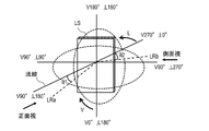
- FIG. 1 is a schematic cross-sectional view of a lighting device 100A according to an embodiment of the present invention
- FIG. It is a typical top view of 100 A of illuminating devices.
- FIG. 10 is a schematic cross-sectional view of an internal space 64A that the lighting device 100A may have;
- 6 is a schematic plan view of an internal space 64A;
- FIG. It is a schematic plan view showing a variation of the internal space 64A.
- It is a graph which shows the example of the shape of the curved surface of the 1st inclined surface ISa of 64 A of internal spaces.
- It is a figure which shows the coordinate system for expressing the light distribution of the emitted light of an illuminating device.
- FIG. 5 is a graph showing the light distribution in the V direction of light emitted from the lighting device of Example 1.
- FIG. 5 is a graph showing the light distribution in the L direction of light emitted from the lighting device of Example 1.
- FIG. 9 is a graph showing the light distribution in the V direction of light emitted from the lighting device of Example 2.
- FIG. 9 is a graph showing the light distribution in the L direction of light emitted from the lighting device of Example 2.
- FIG. 10 is a graph showing the light distribution in the V direction of light emitted from the illumination device of Example 3.
- FIG. 10 is a graph showing the light distribution in the L direction of light emitted from the lighting device of Example 3.
- FIG. 10 is a graph showing the light distribution in the V direction of the light emitted from the lighting device of Example 4 according to the embodiment of the present invention;
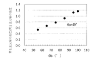
- FIG. 10 is a graph showing the results obtained by simulation of the value of the intensity of the first principal ray/the intensity of the second principal ray when the inclination angle ⁇ a of the internal space 64A is changed.
- FIG. 10 is a graph showing the result of simulation of the ratio of the intensity of the first principal ray to the intensity of the second principal ray when the inclination angle ⁇ a of the internal space 64A of the lighting device of Example 3 is changed.
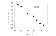
- FIG. 10 is a graph showing the results obtained by simulation of the ratio of the intensity of the first principal ray to the intensity of the second principal ray when the inclination angle ⁇ b of the internal space 64A of the lighting device of Example 3 is changed.
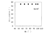
- 10 is a graph showing the first principal ray direction (polar angle ⁇ 1) when the inclination angle ⁇ a of the internal space 64A of the lighting device of Example 3 is changed.
- FIG. 10 is a graph showing the first principal ray direction (polar angle ⁇ 1) when the inclination angle ⁇ b of the internal space 64A of the lighting device of Example 3 is changed.
- 10 is a graph showing the second principal ray direction (polar angle ⁇ 2) when the inclination angle ⁇ a of the internal space 64A of the lighting device of Example 3 is changed.
- 10 is a graph showing the second principal ray direction (polar angle ⁇ 2) when the inclination angle ⁇ b of the internal space 64A of the lighting device of Example 3 is changed.
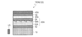
- FIG. 10 is a schematic cross-sectional view of another lighting device 100A1 according to an embodiment of the present invention
- FIG. 10 is a schematic cross-sectional view of still another lighting device 100A2 according to an embodiment of the present invention;
- FIG. 10 is a schematic cross-sectional view of still another illumination device 100A3 according to an embodiment of the present invention
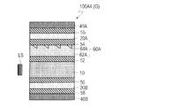
- FIG. 10 is a schematic cross-sectional view of still another illumination device 100A4 according to an embodiment of the present invention
- FIG. 10 is a schematic cross-sectional view of still another lighting device 100B1 according to an embodiment of the present invention
- FIG. 11 is a schematic cross-sectional view of still another lighting device 100B2 according to an embodiment of the present invention
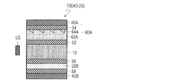
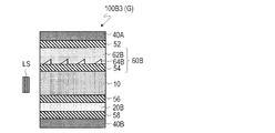
- FIG. 11 is a schematic cross-sectional view of still another lighting device 100B3 according to an embodiment of the present invention
- FIG. 10 is a schematic cross-sectional view of still another illumination device 100B4 according to an embodiment of the present invention
- FIG. 11 is a schematic cross-sectional view of still another lighting device 100A3_1 according to an embodiment of the present invention
- FIG. 10 is a schematic cross-sectional view of still another lighting device 100A3_2 according to an embodiment of the present invention
- a light guide member for a lighting device and a lighting device according to embodiments of the present invention will be described below with reference to the drawings.
- the light guide member for a lighting device and the lighting device according to the embodiments of the present invention are not limited to those exemplified below.
- FIG. 1 shows a schematic cross-sectional view of a lighting device 100A according to an embodiment of the present invention.
- the lighting device 100A is a sheet-like lighting device having two exit surfaces facing in opposite directions.
- the illumination device 100A has a first emission surface (lower in FIG. 1) for emitting the first light LRa and a second emission surface (upper in FIG. 1) for emitting the second light LRb.
- the first light LRa is emitted in the -Z direction in FIG. 1, and the second light LRb is emitted in the Z direction.
- the lighting device 100A has a light source LS and a lighting device light guide member 100A (G).
- the light guide member for the lighting device is represented by adding (G) after the reference numeral of the lighting device 100A.
- the lighting device light guide member 100A(G) has a light receiving portion that receives light emitted from the light source LS, a first main surface on the side of the first emission surface, and a second main surface on the side of the second emission surface. It has a light guide layer 10 and a light distribution control structure having a plurality of internal spaces 64A.
- the light receiving portion of the lighting device light guide member 100A(G) is, for example, the side surface (light receiving side surface) of the light guide layer 10 on the light source LS side.
- Each of the plurality of internal spaces 64A includes a first inclined surface ISa that directs part of the light propagating in the light guide layer 10 toward the first emission surface side by total internal reflection (TIR), and the first inclined surface ISa and a second inclined surface ISb on the opposite side.
- the second light LRb emitted from the second emission surface is light that has entered the internal space 64A from the first inclined surface ISa and passed through the internal space 64A.
- the second light LRb is transmitted through the upper surface of the internal space 64A (the interface with the adhesive layer 54) or the second inclined surface ISb.
- the first light LRa and the second light LRb can be refracted according to the refractive index of the material forming the interface when passing through the interface.
- the light distribution control structure having a plurality of internal spaces 64A is formed in the direction conversion layer 60A arranged on the second main surface side of the light guide layer 10.
- a redirecting layer 60A having a plurality of internal spaces 64A is composed of a shaping film 62A having recesses 64A (indicated by the same reference numerals as the internal spaces 64A) on the surface and an adhesive layer .
- the internal space 64A is not limited to this example. For example, as described later with reference to FIG. good.
- a plurality of internal spaces 64A (or internal spaces 64B in FIG. 17A and the like) may be formed within the light guide layer 10 .
- the lighting device light guide member 100A(G) emits the first light LRa having the first light distribution from the first emission surface and the second light distribution from the second emission surface by the light distribution control structure. It is configured to emit second light LRb having a distribution.
- the intensity of the first principal ray when the ray with the highest intensity in the first light distribution is set as the first principal ray and the ray with the highest intensity in the second light distribution is set as the second principal ray, for example, the intensity of the first principal ray :
- the intensity of the second chief ray can be controlled within the range of 1:4 to 4:1.
- the intensity of the first principal ray/the intensity of the second principal ray is, for example, within the range of 0.5 or more and 1.3 or less. Therefore, both the first light LRa and the second light LRb can be used for illumination.
- the polar angle ⁇ 1 of the first principal ray from the normal to the first exit surface is smaller than the polar angle ⁇ 2 of the second principal ray from the normal to the second exit surface.
- the polar angle ⁇ 1 is 0° or more and less than 40°
- the polar angle ⁇ 2 is 30° or more and less than 70°.
- the first light distribution and the second light distribution are obtained by adjusting the cross-sectional shape, planar shape, size, arrangement density, and distribution of the internal space 64A (or the internal space 64B in FIG. 17A and the like). can be controlled. As will be described later with reference to FIG.
- the inclination angle ⁇ a of the first inclined surface ISa is 10° or more and 70° or less.
- the inclination angle ⁇ b of the second inclined surface ISb is 50° or more and 100° or less.
- the cross-sectional shape of the internal space 64A is triangular as exemplified here, but is not limited to this and may be trapezoidal or the like.
- the lighting device light guide member 100A(G) may have, for example, a visible light transmittance of 60% or more and a haze value of less than 30%.
- the visible light transmittance is preferably 70% or more, more preferably 80% or more.
- the haze value is preferably less than 10%, more preferably 5% or less.
- the lighting device light guide member 100A(G) according to the embodiment of the present invention has a high visible light transmittance and a low haze value. can see.
- light with a wavelength of 380 nm or more and 780 nm or less is defined as visible light.
- Visible light transmittance and haze value can be measured using, for example, a haze meter (manufactured by Murakami Color Research Laboratory: trade name HM-150).
- the plurality of internal spaces 64A which are the light distribution control structure, have a ratio of the area of the plurality of internal spaces 64A to the area of the light guide layer 10 (occupied area rate) is preferably 1% or more and 80% or less, the upper limit is more preferably 50% or less, further preferably 45% or less, and in order to obtain a high transmittance and / or a low haze value, 30% or less It is preferably 10% or less, more preferably 5% or less.
- the occupied area ratio of the internal space 64A may be uniform, or the occupied area ratio should increase as the distance from the light source LS increases so that the brightness does not decrease. good too.
- the occupied area ratio of the internal space 64A is uniform.
- the shaped film 62A is adhered to the second main surface of the light guide layer 10 by the adhesive layer 52, and the shaped film 62A and the direction changing layer 60A are formed by bonding.
- the base material layer 30 and the shaped film 62A are adhered by the agent layer 54 .
- the light guide layer 10 and the substrate layer 30 may be transparent substrates or films. Preferred configurations of the light guide layer 10, base layer 30, shaped film 62A, and adhesive layers 52 and 54 will be described later.
- FIG. 2 shows a schematic plan view of the illumination device 100A.
- the plurality of internal spaces 64A are discretely arranged, for example, in the light guide direction (Y direction) of the light guide layer 10 and in the direction (X direction) perpendicular to the light guide direction.
- the size of the internal space 64A (length L, width W: see FIGS. 3A and 3B)
- the length L is preferably 10 ⁇ m or more and 500 ⁇ m or less
- the width W is preferably 1 ⁇ m or more and 100 ⁇ m or less.
- the height H is preferably 1 ⁇ m or more and 100 ⁇ m or less.
- the plurality of internal spaces 64A are discretely arranged in the light guide direction (Y direction) of the light guide layer 10 and in the direction (X direction) orthogonal to the light guide direction.
- the plurality of internal spaces 64A can be discretely arranged in the light guide direction (Y direction) of the light guide layer 10 and in a direction crossing the light guide direction.
- the discrete arrangement of the internal spaces 64A can be appropriately set according to the shape of the light guide layer 10, the required light distribution, and the like.
- the Y direction is referred to as the light guide direction
- light having a component in the Y direction (not zero) propagates in the Y direction. to The same applies to other directions. That is, light propagating in the -Y direction includes all light having a -Y direction component (not zero).
- the plurality of internal spaces 64 are discretely arranged, for example, in the light guide direction and in a direction intersecting the light guide direction.
- the discrete arrangement may or may not have periodicity (regularity) in at least one direction.
- a plurality of internal spaces 64 having substantially the same shape and convex curved surfaces in the same direction are formed in the light guiding direction (Y direction) of the light guide layer 10 and in the light guiding direction. They are arranged discretely and periodically in the entire area in the orthogonal direction (X direction).
- the pitch Px is preferably, for example, 10 ⁇ m or more and 500 ⁇ m or less
- the pitch Py is, for example, preferably 10 ⁇ m or more and 500 ⁇ m or less.
- the example shown in FIG. 2 further has internal spaces arranged with a half pitch shift in each of the Y and X directions.
- Px is 200 ⁇ m and Py is 100 ⁇ m
- Px is 260 ⁇ m and Py is 160 ⁇ m.
- the first inclined surface ISa forms a curved surface convex toward the light source LS.
- the light source LS is, for example, an LED device, and a plurality of LED devices are arranged in the X direction. Since the light emitted from each of the plurality of LED devices spreads in the Y direction, it is preferable that the first inclined surface ISa has a curved surface convex toward the light source LS side.
- the first inclined surface ISa may be parallel to the X direction.
- internal spaces such as grooves (for example, triangular prisms) extending in the X direction may be used.
- FIG. 3A is a schematic cross-sectional view of the internal space 64A
- FIG. 3B is a schematic plan view of the internal space 64A
- FIG. 3C is a schematic plan view showing variations of the internal space 64A.
- FIG. 4 is a graph showing an example of the shape of the curved surface of the first inclined surface ISa of the internal space 64A.
- the cross-sectional shape of the internal space 64A is, for example, triangular.
- the inclination angle ⁇ a of the first inclined surface ISa on the light source LS side is, for example, 10° or more and 70° or less. If the angle of inclination ⁇ a is less than 10°, the controllability of the light distribution may deteriorate, and the light extraction efficiency may also deteriorate. On the other hand, if the inclination angle ⁇ a exceeds 70°, it may become difficult to process the shaped film, for example. Also, the inclination angle ⁇ b of the second inclined surface ISb is, for example, 50° or more and 100° or less.
- the internal space 64A preferably has a length L of 10 ⁇ m or more and 500 ⁇ m or less, and a width W of 1 ⁇ m or more and 100 ⁇ m or less.
- the length L is, for example, twice the width W or more.
- the height H is preferably 1 ⁇ m or more and 100 ⁇ m or less.
- the recesses having the planar shape shown in FIG. 3C may be formed. Even in such a case, the planar shape of the internal space can be characterized by the length L and width W.
- the convex curved surface of the first inclined surface ISa toward the light source LS is represented by the graph shown in FIG. 4, for example.
- the length L is 60 ⁇ m
- the inclination angles ⁇ a of the first inclined surface ISa are 30°, 40°, and 49°
- the internal space in which the first inclined surface ISa forms a curved surface shown in FIG. A lighting device with 64A was made.
- the width W was about 13.9 ⁇ m, about 9.5 ⁇ m, and about 7.0 ⁇ m in Examples 1-3, respectively.
- the curved surface shown in FIG. 4 is represented by, for example, a quartic curve.
- the inclination angle ⁇ b of the second inclined surface ISb was set to 85° in all of Examples 1-3.
- the lighting devices of Examples 1 to 3 have substantially the same structure as the lighting device 100A shown in FIG. In Example 4, the same shaped film as in Example 3 was used, and the illumination device had a simple configuration in which the base layer 30 and the adhesive layer 54 in FIG. 1 were omitted.
- the size of the shaped film in the lighting device of Examples 1 to 3 (longitudinal direction: light guide direction x width direction) was about 600 mm x about 700 mm, whereas the size of the shaped film in the lighting device of Example 4
- the size (longitudinal direction: light guiding direction ⁇ width direction) was about 170 mm ⁇ about 120 mm.
- FIG. 5 shows a coordinate system showing the 3D light distribution of the emitted light from the lighting device.
- the first light distribution of the first light emitted from the first emission surface in each lighting device is represented by the polar angle ⁇ 1 from the normal to the first emission surface of the first principal ray, and the second emission surface
- the second light distribution of the second light emitted from is represented by the polar angle ⁇ 2 from the normal to the second emission surface of the second principal ray.
- the ray with the highest intensity in the first light distribution is referred to as the first principal ray
- the ray with the highest intensity in the second light distribution is referred to as the second principal ray.
- the light distribution in each lighting device of Examples 1 to 3 was measured using a light distribution measuring device (manufactured by PIMACS, Neolight 9500).
- the light distribution in the lighting device of Example 4 was measured using a light distribution evaluation device (Radiant Conoscope 070 manufactured by Radiant Vision Systems).
- the side from which the first light LRa is emitted is the front side
- the side from which the second light LRb is emitted is the back side
- the polar angle in the V direction is sometimes simply denoted as V
- the polar angle in the L direction is sometimes simply denoted as L.
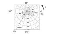
- FIG. 6A shows the light distribution of light emitted from the lighting device of Example 1.
- FIG. 6B is a graph showing the light distribution in the V direction of light emitted from the lighting device of Example 1
- FIG. 6C is a graph showing the light distribution in the L direction of light emitted from the lighting device of Example 1.
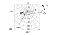
- FIG. 7A shows the light distribution of light emitted from the illumination device of Example 2.
- FIG. 7B is a graph showing the light distribution in the V direction of light emitted from the lighting device of Example 2
- FIG. 7C is a graph showing the light distribution in the L direction of light emitted from the lighting device of Example 2.
- FIG. 8A shows the light distribution of light emitted from the illumination device of Example 3.
- FIG. 8A shows the light distribution of light emitted from the illumination device of Example 3.
- FIG. 8B is a graph showing the light distribution in the V direction of light emitted from the lighting device of Example 3
- FIG. 8C is a graph showing the light distribution in the L direction of light emitted from the lighting device of Example 3.
- FIG. 8D is a graph showing the light distribution in the V direction of the light emitted from the lighting device of Example 4. As shown in FIG.
- the polar angle ⁇ 1 in the light distribution of the lighting device of Example 1 is about 30°, and the polar angle ⁇ 2 is about 48°.
- the half maximum (FWHM) angle in the V direction is about 67° and the half maximum angle in the L direction is about 94°.
- the polar angle ⁇ 1 in the light distribution of the illumination device of Example 2 is approximately 10°, and the polar angle ⁇ 2 is approximately 60°.
- the half maximum (FWHM) angle in the V direction is about 54° and the half maximum angle in the L direction is about 94°.
- the polar angle ⁇ 1 in the light distribution of the illumination device of Example 3 is approximately 8°, and the polar angle ⁇ 2 is approximately 58°.
- the half maximum (FWHM) angle in the V direction is approximately 45°, and the half maximum angle in the L direction is approximately 86°.
- the polar angle ⁇ 1 from the normal to the first exit surface of the first principal ray LRa is the normal to the second exit surface of the second principal ray LRb.
- the half-value angle in the V direction can be reduced to at least about 24°.
- the half-value angle of the first light in the V direction is about 45° or more and about 67° or less
- the half-value angle of the second light in the L direction is about 86° or more and about 94°. It can be controlled within the range of °.
- the lower limit of the half-value angle in the V direction of the first light can be reduced to at least about 24°.
- Table 1 shows the ratio of the intensity of the first principal ray to the intensity of the second principal ray, the polar angle ⁇ 1, the half-value angle in the V direction, and the half-value angle in the L direction in each lighting device of Examples 1 to 4.
- Table 1 also shows the inclination angles ⁇ a and ⁇ b and the ratio of the area of the internal space to the area of the light guide layer (internal space occupied area ratio).
- the value of the intensity of the first principal ray/the intensity of the second principal ray is in the range of 0.9 or more and 1.3 or less, and both sides of the sheet-shaped lighting device are illuminated. I know you can.
- the ratio of the intensity of the first principal ray to the intensity of the second principal ray can be increased as the internal space occupation area ratio is increased.
- the internal space occupied area ratios were all 5% or less, and they had a visible light transmittance of 80% or more and a haze value of 5% or less.
- FIG. 9 shows the results obtained by simulation of the value of the intensity of the first principal ray/the intensity of the second principal ray when the inclination angle ⁇ a of the internal space 64A is changed, together with the results of actual measurements in Examples 1 to 3 above. ,show.
- the internal space occupation area ratio was set to 1.20%.
- the value of the intensity of the first principal ray/the intensity of the second principal ray in Example 3, in which the internal space occupancy is 1.20% roughly agrees with the simulation results.
- the value of the intensity of the first principal ray/the intensity of the second principal ray has a minimum value when the inclination angle ⁇ a is about 45°, and is larger than about 45° (for example, about 49°). greater than or equal to) or small (e.g., about 40° or less). Therefore, by adjusting the internal space occupation ratio and the inclination angle ⁇ a, the value of the intensity of the first principal ray/the intensity of the second principal ray can be changed.
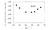
- Table 2 below and FIG. 10 show the results obtained by simulating the values of the intensity of the first principal ray/the intensity of the second principal ray when the inclination angle ⁇ a of the internal space 64A of the lighting device of Example 3 is changed. show.
- FIG. 11 shows the results obtained by simulation of the ratio of the intensity of the first principal ray to the intensity of the second principal ray when the inclination angle ⁇ b of the internal space 64A of the lighting device of Example 3 is changed.
- the internal space occupation area ratio was set to 1.20%.
- FIGS. 10 and 11 by changing the inclination angles ⁇ a and ⁇ b, the value of the intensity of the first principal ray/the intensity of the second principal ray can be reduced within the range of 0.5 to 1.3. can be adjusted with Furthermore, by adopting a configuration in which a light absorption layer is provided on the light incident side, which will be described later with reference to FIGS. : can be controlled within the range of 1 or less.
- FIG. 12 shows the first principal ray direction (polar angle ⁇ 1) when the inclination angle ⁇ a of the internal space 64A of the lighting device of the third embodiment is changed, and the first principal ray direction when the inclination angle ⁇ b is changed.
- (Polar angle ⁇ 1) is shown in FIG.
- the first principal ray direction (polar angle ⁇ 1) can be changed by changing the inclination angle ⁇ a.
- the tilt angle ⁇ b does not affect the direction of the first principal ray (polar angle ⁇ 1).
- FIG. 14 shows the second principal ray direction (polar angle ⁇ 2) when the inclination angle ⁇ a of the internal space 64A of the lighting device of the third embodiment is changed, and the second principal ray direction when the inclination angle ⁇ b is changed.
- (polar angle ⁇ 2) is shown in FIG.
- the second principal ray direction (polar angle ⁇ 2) can be changed by changing the inclination angle ⁇ a.
- the tilt angle ⁇ b does not affect the second principal ray direction (polar angle ⁇ 2).
- the light distribution of the emitted light of the illumination device can be adjusted by adjusting the internal space occupation area ratio and the inclination angles ⁇ a and ⁇ b.
- the tilt angle ⁇ b does not affect the direction of the chief ray (polar angles ⁇ 1 and ⁇ 2), but almost linearly affects the ratio of the intensity of the first chief ray to the intensity of the second chief ray (see FIG. 11). . Therefore, the ratio between the intensity of the first principal ray and the intensity of the second principal ray can be adjusted by changing the inclination angle ⁇ b after determining the internal space occupation area ratio and the inclination angle ⁇ a.
- Illumination devices 100A1, 100A2, 100A3, and 100A4 shown in FIGS. 16A, 16B, 16C, and 16D are arranged so that the first emission surface faces downward, similar to illumination device 100A shown in FIG.
- Illumination device light guide member 100A1 (G) of illumination device 100A1 shown in FIG. It has a layer 40A.
- a hard coat layer for example, a pencil hardness of H or more
- an antireflection layer and a hard coat layer may be provided.
- an antireflection layer and/or a hard coat layer may be provided on the first main surface (lower side) of the light guide layer 10 .
- the antireflection layer and the hard coat layer can be formed by known methods using known materials. These are common to other exemplary lighting devices.
- the lighting device light guide member 100A2 (G) of the lighting device 100A2 shown in FIG. 16B further has a low refractive index layer 20A on the second exit surface side of the direction changing layer 60A.
- a low refractive index layer 20B may be provided on the first main surface (lower side) of the light guide layer 10, as in the lighting device light guide member 100A3 (G) of the lighting device 100A3 shown in FIG. 16C.
- a low refractive index layer 20B may be provided on one main surface (lower side). Adhesive layers 52, 55, 56, and 58 may be appropriately provided as necessary when providing the antireflection layer, hard coat layer, and low refractive index layer.
- lighting devices 100B1, 100B2, 100B3, and 100B4 shown in FIGS. 17A, 17B, 17C, and 17D are configured so that the first emission surface faces upward, unlike the lighting device 100A shown in FIG. 1 shows an example of a lighting device including lighting device light guide members 100B1(G), 100B2(G), 100B3(G) and 100B4(G) having a light distribution control structure (that is, a plurality of internal spaces 64B). .
- the lighting device light guide member 100B1 (G) of the lighting device 100B1 shown in FIG. It has a layer 60B.
- the direction changing layer 60B is composed of a shaping film 62B having recesses 64B (indicated by the same reference numerals as the internal space 64B) on the surface and the adhesive layer 54.
- a light distribution control structure may be formed in the light guide layer 10 .
- the illumination device 100B1 has an antireflection layer 40A on the first emission surface side of the direction changing layer 60B.
- a hard coat layer for example, a pencil hardness of H or more
- an antireflection layer and a hard coat layer may be provided.
- the lighting device light guide member 100B2 (G) of the lighting device 100B2 shown in FIG. 17B further has a low refractive index layer 20A on the first exit surface side of the direction changing layer 60B.
- a low refractive index layer 20B may be provided on the second main surface (lower side) of the light guide layer 10 as in a lighting device light guide member 100B3 (G) of a lighting device 100B3 shown in FIG. 17C.
- a low refractive index layer 20B may be provided on the two main surfaces (lower side).
- FIG. 18A shows a schematic cross-sectional view of still another lighting device 100A3_1 according to the embodiment of the present invention
- FIG. 18B shows a schematic cross-sectional view of still another lighting device 100A3_2 according to the embodiment of the present invention
- Lighting device 100A3_1 and lighting device 100A3_2 are modified examples of lighting device 100A3 shown in FIG. 16C. Other lighting devices described above may be similarly modified.
- Illumination device light guide member 100A3_1(G) of illumination device 100A3_1 shown in FIG. It has light absorption layers 70A and 70B at the end of the light exit surface) on the light source LS side.
- the light absorption layers 70A and 70B are layers that absorb visible light and exhibit a black color, and may be black adhesive tapes, for example.
- the light absorption layers 70A and 70B have a width of, for example, about 10 mm from the light source LS side, and extend along the light receiving portion of the lighting device light guide member 100A3_1(G) (for example, the lighting device guide shown in FIG. 2). (along the short side of the optical member 100A(G)).
- the illumination device light guide member 100A3_1(G) of the illumination device 100A3_1 shown in FIG. 18A is the first emission surface and the second emission surface (
- Light absorption layers 70A and 70B are provided at the ends of the light source LS side of the upper and lower exit surfaces.
- the light absorption layers 70A and 70B are layers that absorb visible light and exhibit a black color, and may be black adhesive tapes, for example.
- the light absorption layers 70A and 70B have a width of, for example, about 10 mm from the light source LS side, and extend along the light receiving portion of the lighting device light guide member 100A3_1 (G) (for example, the lighting device light guide member shown in FIG. 2). (along the short side of the member 100A(G)).
- the light absorption layers 70A and 70B absorb part of the light incident on the light guide layer 10 from the light source LS. Without the light absorption layers 70A and 70B, the light absorbed by the light absorption layers 70A and 70B is emitted from the first emission surface and the second emission surface near the end of the lighting device light guide member 100A3_1(G) on the light source LS side. It includes light that is totally reflected (at the interface with air) and returns to the lighting device light guide member 100A3_1 (G). Therefore, by providing the light absorption layers 70A and 70B and adjusting their widths, the incident angles of the light propagating through the lighting device light guide member 100A3_1(G) with respect to the first emission surface and the second emission surface are limited. be able to.
- the ratio of the intensity of the first principal ray to the intensity of the second principal ray can be controlled within a range of 1:4 or more and 4:1 or less.
- the width of the light absorption layers 70A and/or 70B may be appropriately set independently.
- the first and second major surfaces of the section have exposed portions and have light absorbing layers 70A and 70B on the exposed first and second major surfaces.
- the light absorption layers 70A and 70B absorb part of the light incident on the light guide layer 10 from the light source LS.
- the light absorbed by the light absorption layers 70A and 70B is totally reflected by the exposed first and second surfaces (interfaces with air) of the light guide layer 10 without the light absorption layers 70A and 70B. Including light propagating in 10 .
- the incident angles of the light propagating in the light guide layer 10 with respect to the first and second main surfaces of the light guide layer 10 are limited. be able to.
- the ratio of the intensity of the first principal ray to the intensity of the second principal ray can be controlled within a range of 1:4 or more and 4:1 or less. Note that only one of the light absorption layers 70A and 70B may be provided, and the width of the light absorption layers 70A and/or 70B may be appropriately set independently.
- the low refractive index layers 20A and 20B and the hard coat layers and/or antireflection layers 40A and 40B are respectively It has a substrate layer on the adhesive layer side.
- the substrate layers serve to support the low refractive index layer and the hard coat layer and/or antireflection layer, respectively.
- the thickness of each substrate layer is independently, for example, 1 ⁇ m or more and 1000 ⁇ m or less, preferably 10 ⁇ m or more and 100 ⁇ m or less, and more preferably 20 ⁇ m or more and 80 ⁇ m.
- the refractive indices of the substrate layers are preferably 1.40 or more and 1.70 or less, and more preferably 1.43 or more and 1.65 or less.
- a base material layer is an acrylic film, for example.
- a shaping film for forming an internal space can be manufactured, for example, as follows.
- a concave-convex shaped film was produced according to the method described in JP-T-2013-524288. Specifically, the surface of a polymethyl methacrylate (PMMA) film is coated with lacquer (Fine Cure RM-64 manufactured by Sanyo Chemical Industries, Ltd.), an optical pattern is embossed on the film surface containing the lacquer, and then the lacquer is applied. was cured to produce the desired concave-convex shaped film. The total thickness of the concave-convex shaped film is 130 ⁇ m.
- the light guide layer 10 is made of a known material with high visible light transmittance.
- the light guide layer 10 is made of, for example, an acrylic resin such as polymethyl methacrylate (PMMA), a polycarbonate (PC) resin, a cycloolefin resin, or glass (for example, quartz glass, alkali-free glass, or borosilicate glass). be.
- the refractive index n GP of the light guide layer 10 is, for example, 1.40 or more and 1.80 or less. Unless otherwise specified, the refractive index refers to the refractive index measured with an ellipsometer at a wavelength of 550 nm.
- the thickness of the light guide layer 10 can be appropriately set according to the application.
- the thickness of the light guide layer 10 is, for example, 0.05 mm or more and 50 mm or less.
- the thickness of the base material layer is, for example, 1 ⁇ m or more and 1000 ⁇ m or less, preferably 10 ⁇ m or more and 100 ⁇ m or less, and more preferably 20 ⁇ m or more and 80 ⁇ m or less.
- the refractive indices of the substrate layers are preferably 1.40 or more and 1.70 or less, and more preferably 1.43 or more and 1.65 or less.
- the thicknesses of the adhesive layers 52, 54, 55, 56, and 58 are each independently, for example, 0.1 ⁇ m or more and 100 ⁇ m or less, preferably 0.3 ⁇ m or more and 100 ⁇ m or less, and more preferably 0.5 ⁇ m or more and 50 ⁇ m or less.
- the adhesive layers 52, 54, 55, 56, and 58 each independently have a refractive index of preferably 1.42 or more and 1.60 or less, more preferably 1.47 or more and 1.58 or less.
- the refractive index of the adhesive layers 52, 54, 56, 58 is preferably close to the refractive index of the light guide layer 10 or the shaping film 62A or 62B with which it is in contact, and the absolute value of the refractive index difference is 0.5. It is preferably 2 or less.
- the adhesive layer 54 can adhere without filling the concave portions 64A or 64B on the surface of the shaping film 62A or 62B.
- the adhesive described in International Application PCT/JP2021/006452, International Application PCT/JP2021/006453, or Japanese Patent Application No. 2021-025496 by the present applicant can be preferably used. can be done. The entire disclosure of these applications is incorporated herein by reference.
- the polyester-based adhesive described in Japanese Patent Application No. 2021-025496 is preferable.
- the refractive indices n L1 of the low refractive index layers 20A and 20B are each independently preferably, for example, 1.30 or less, more preferably 1.20 or less, and even more preferably 1.15 or less.
- the low refractive index layers 20A and 20B are preferably solid, and preferably have a refractive index of, for example, 1.05 or more.
- the difference between the refractive index of the light guide layer 10 and the refractive index layers of the low refractive index layers 20A and 20B is preferably 0.20 or more, more preferably 0.23 or more, and still more preferably 0.25 or more. is.
- the low refractive index layers 20A and 20B having a refractive index of 1.30 or less can be formed using, for example, a porous material.
- the thicknesses of the low refractive index layers 20A and 20B are each independently, for example, 0.3 ⁇ m or more and 5 ⁇ m or less.
- the porosity is preferably 35% by volume or more, more preferably 38% by volume or more, and particularly preferably 40% by volume or more. . Within such a range, a low refractive index layer having a particularly low refractive index can be formed.
- the upper limit of the porosity of the low refractive index layer is, for example, 90% by volume or less, preferably 75% by volume or less. Within such a range, a low refractive index layer having excellent strength can be formed.
- the porosity is a value calculated by Lorentz-Lorenz's formula from refractive index values measured by an ellipsometer.
- the low refractive index layer for example, a low refractive index layer having voids disclosed in Patent Document 3 can be used.
- the low refractive index layer having voids is a porous body formed by directly chemically bonding particles (for example, microporous particles) to each other.
- the particles constituting the low refractive index layer having voids may be bonded together via a small amount (for example, the mass of the particles or less) of one component of the binder.
- the porosity and refractive index of the low refractive index layer can be adjusted by the particle size, particle size distribution, etc. of the particles forming the low refractive index layer.
- Methods for obtaining a low refractive index layer having voids include, for example, JP-A-2010-189212, JP-A-2008-040171, JP-A-2006-011175, International Publication No. 2004/113966, and their Methods described in ref. All of the disclosures of JP-A-2010-189212, JP-A-2008-040171, JP-A-2006-011175, and International Publication No. 2004/113966 are incorporated herein by reference.
- a silica porous material can be preferably used as the low refractive index layer having voids.
- a silica porous body is produced, for example, by the following method. a silicon compound; hydrolyzable silanes and/or silsesquioxane, and a method of hydrolyzing and polycondensing at least one of its partial hydrolyzate and dehydration condensate; porous particles and/or hollow fine particles; method, method of generating an airgel layer using the springback phenomenon, pulverizing the gel-like silicon compound obtained by the sol-gel method, and chemically pulverizing the resulting pulverized microporous particles with a catalyst or the like. and a method using a combined pulverized gel.
- the low refractive index layer is not limited to the porous silica material, nor is the manufacturing method limited to the exemplified manufacturing method, and may be manufactured by any manufacturing method.
- the porous layer is not limited to the silica porous body, and the manufacturing method is not limited to the exemplified manufacturing method, and may be manufactured by any manufacturing method.
- Silsesquioxane is a silicon compound having (RSiO 1.5 , R is a hydrocarbon group) as a basic structural unit, and is strictly different from silica having SiO 2 as a basic structural unit.
- a porous material containing silsesquioxane as a basic structural unit is also referred to herein as a silica porous material or a silica-based porous material, since it has a network structure crosslinked with silica in common.
- the silica porous body can be composed of microporous particles of a gel-like silicon compound bonded together.
- pulverized bodies of the gelled silicon compound can be mentioned.
- the silica porous body can be formed, for example, by coating a base material with a coating liquid containing a pulverized gel-like silicon compound.
- the pulverized gel-like silicon compound can be chemically bonded (for example, siloxane bond) by the action of a catalyst, light irradiation, heating, or the like.
- the hardness HH1 of the hard coat layers 40A and 40B is, for example, preferably a pencil hardness of H or more, more preferably 2H or more, and more preferably 4H or more.
- the upper limit of the hardness HH1 of the hard coat layers 40A and 40B is not particularly limited, but the pencil hardness is preferably 6H or less, more preferably 5H or less. Pencil hardness is measured by a method conforming to JIS K 5400 "Pencil Hardness Test".
- the hard coat layers 40A and 40B each independently have a thickness of preferably 1 ⁇ m or more and 30 ⁇ m or less, more preferably 2 ⁇ m or more and 20 ⁇ m or less, and still more preferably 3 ⁇ m or more and 15 ⁇ m or less. If the thickness of the hard coat layers 40A and 40B is within this range, they have good scratch resistance.
- the hard coat layers 40A and 40B can be made of any suitable material as long as the properties as described above are satisfied.
- the hard coat layers 40A and 40B are, for example, cured layers of thermosetting resin or ionizing radiation (eg, visible light, ultraviolet) curable resin.
- curable resins include acrylates such as urethane (meth)acrylate, polyester (meth)acrylate and epoxy (meth)acrylate, silicon resins such as polysiloxane, unsaturated polyesters, and epoxy resins.
- the hard coat layers 40A and 40B can be formed, for example, by applying a material containing a solvent and a curable compound to the surface of the target substrate and curing the material. Details of the hard coat layers suitably used as the hard coat layers 40A and 40B are described, for example, in JP-A-2011-237789. The entire disclosure of JP-A-2011-237789 is incorporated herein by reference.
- the sheet-shaped lighting device has a high visible light transmittance, so it can be used as a window that can be illuminated.
- it can be used as an illumination window for indoor use and as a device for emitting light downward (or upward) for outdoor use.
- light emitted to the outside of a window can be used for advertising.
- a lighting device according to an embodiment of the present invention can emit light from two main surfaces facing in opposite directions.
- a lighting device according to embodiments of the present invention can provide new applications.
- 10 light guide layer 60A, 60B: direction changing layer 20A, 20B: low refractive index layer 30: substrate layer 40A, 40B: hard coat layer and/or antireflection layer 52, 54, 55, 56 , 58: adhesive layer, 62A, 62B: shaped film, 64A, 64B: internal space, recessed portion, 100A: lighting device, 100A (G): light guide member for lighting device, ISa: first inclined surface, ISb: Second inclined surface, LRa: first light, LRb: second light, LS: light source
Abstract
Description
[項目1]
第1出射面と、前記第1出射面とは反対側の第2出射面とを有する照明装置用導光部材であって、
光源から出射された光を受ける受光部と、
前記第1出射面側の第1主面と、前記第2出射面側の第2主面とを有する導光層と、
複数の内部空間を有する配光制御構造と
を有し、
前記複数の内部空間のそれぞれは、前記導光層内を伝搬する光の一部を内部全反射によって前記第1出射面側に向ける第1傾斜面と、前記第1傾斜面とは反対側の第2傾斜面とを有し、
前記第1出射面から第1の配光分布を有する第1の光を出射し、前記第2出射面から第2の配光分布を有する第2の光を出射するように構成されている、照明装置用導光部材。
[項目2]
前記第1の配光分布において強度の最も大きい光線を第1主光線とし、前記第2の配光分布において強度の最も大きい光線を第2主光線とするとき、前記第1主光線の強度:前記第2主光線の強度は、1:4以上4:1以下の範囲内にある、項目1に記載の照明装置用導光部材。
[項目3]
前記第1主光線の強度/前記第2主光線の強度は、0.5以上1.3以下の範囲内にある、項目2に記載の照明装置用導光部材。
[項目4]
前記第1主光線の前記第1出射面に対する法線からの極角θ1は、前記第2主光線の前記第2出射面に対する法線からの極角θ2よりも小さい、項目2または3に記載の照明装置用導光部材。
[項目5]
前記極角θ1は、0°以上40°未満であり、前記極角θ2は、30°以上70°未満である、項目4に記載の照明装置用導光部材。
[項目6]
前記第1主光線の前記導光層の導光方向における半値角は、67°以下である、項目1から5のいずれかに記載の照明装置用導光部材。
[項目7]
前記第1主光線の前記導光層の導光方向における半値角は、24°以上である、項目1から6のいずれかに記載の照明装置用導光部材。
[項目8]
前記配光制御構造は、前記導光層の前記第1主面側または前記第2主面側に配置された方向変換層に形成されている、項目1から7のいずれかに記載の照明装置用導光部材。
[項目9]
前記第1傾斜面の傾斜角度θaは10°以上70°以下である、項目1から8のいずれかに記載の照明装置用導光部材。
[項目10]
前記第2傾斜面の傾斜角度θbは50°以上100°以下である、項目1から9のいずれかに記載の照明装置用導光部材。
[項目11]
前記導光層の前記第1主面に対する法線方向から見たときの、前記導光層の面積に占める前記複数の内部空間の面積の割合は80%以下である、項目1から10のいずれかに記載の照明装置用導光部材。
[項目12]
前記複数の内部空間は、前記導光層の導光方向および前記導光方向と交差する方向に離散的に配置されている、項目1から11のいずれかに記載の照明装置用導光部材。
[項目13]
前記導光層の前記第1主面に対する法線方向から見たとき、前記第1傾斜面は前記光源側に凸な曲面を形成している、項目1から12のいずれかに記載の照明装置用導光部材。
[項目14]
可視光透過率が60%以上であり、ヘイズ値が30%未満である、項目1から13のいずれかに記載の照明装置用導光部材。
[項目15]
項目1から14のいずれかに記載の照明装置用導光部材と、
前記受光部に向けて光を出射する光源と
を備える、照明装置。 According to embodiments of the present invention, solutions are provided in the following items.
[Item 1]
A light guide member for a lighting device having a first emission surface and a second emission surface opposite to the first emission surface,
a light receiving unit that receives light emitted from a light source;
a light guide layer having a first principal surface on the first exit surface side and a second principal surface on the second exit surface side;
a light distribution control structure having a plurality of internal spaces;
Each of the plurality of internal spaces includes a first inclined surface that directs part of the light propagating in the light guide layer toward the first emission surface by total internal reflection, and an opposite side of the first inclined surface. a second inclined surface;
First light having a first light distribution is emitted from the first emission surface, and second light having a second light distribution is emitted from the second emission surface. A light guide member for lighting devices.
[Item 2]
When the ray with the highest intensity in the first light distribution is defined as the first principal ray and the ray with the highest intensity in the second light distribution is defined as the second principal ray, the intensity of the first principal ray: Item 2. The light guide member for an illumination device according to
[Item 3]
Item 3. The light guide member for an illumination device according to item 2, wherein the intensity of the first principal ray/the intensity of the second principal ray is within a range of 0.5 or more and 1.3 or less.
[Item 4]
4. According to item 2 or 3, wherein a polar angle θ1 of the first principal ray from the normal to the first exit surface is smaller than a polar angle θ2 of the second principal ray from the normal to the second exit surface. Light guide member for lighting device of.
[Item 5]
[Item 6]
6. The light guide member for a lighting device according to any one of
[Item 7]
7. The light guide member for a lighting device according to any one of
[Item 8]
8. The lighting device according to any one of
[Item 9]
9. The light guide member for a lighting device according to any one of
[Item 10]
10. The light guide member for a lighting device according to any one of
[Item 11]
11. Any one of
[Item 12]
12. The light guide member for a lighting device according to any one of
[Item 13]
13. The lighting device according to any one of
[Item 14]
14. The light guide member for a lighting device according to any one of
[Item 15]
a light guide member for a lighting device according to any one of
and a light source that emits light toward the light receiving unit.


Claims (15)
- 第1出射面と、前記第1出射面とは反対側の第2出射面とを有する照明装置用導光部材であって、
光源から出射された光を受ける受光部と、
前記第1出射面側の第1主面と、前記第2出射面側の第2主面とを有する導光層と、
複数の内部空間を有する配光制御構造と
を有し、
前記複数の内部空間のそれぞれは、前記導光層内を伝搬する光の一部を内部全反射によって前記第1出射面側に向ける第1傾斜面と、前記第1傾斜面とは反対側の第2傾斜面とを有し、
前記第1出射面から第1の配光分布を有する第1の光を出射し、前記第2出射面から第2の配光分布を有する第2の光を出射するように構成されている、照明装置用導光部材。 A light guide member for a lighting device having a first emission surface and a second emission surface opposite to the first emission surface,
a light receiving unit that receives light emitted from a light source;
a light guide layer having a first principal surface on the first exit surface side and a second principal surface on the second exit surface side;
a light distribution control structure having a plurality of internal spaces;
Each of the plurality of internal spaces includes a first inclined surface that directs part of the light propagating in the light guide layer toward the first emission surface by total internal reflection, and an opposite side of the first inclined surface. a second inclined surface;
First light having a first light distribution is emitted from the first emission surface, and second light having a second light distribution is emitted from the second emission surface. A light guide member for lighting devices. - 前記第1の配光分布において強度の最も大きい光線を第1主光線とし、前記第2の配光分布において強度の最も大きい光線を第2主光線とするとき、前記第1主光線の強度:前記第2主光線の強度は、1:4以上4:1以下の範囲内にある、請求項1に記載の照明装置用導光部材。 When the ray with the highest intensity in the first light distribution is defined as the first principal ray and the ray with the highest intensity in the second light distribution is defined as the second principal ray, the intensity of the first principal ray: 2. The light guide member for an illumination device according to claim 1, wherein the intensity of said second principal ray is within a range of 1:4 or more and 4:1 or less.
- 前記第1主光線の強度/前記第2主光線の強度は、0.5以上1.3以下の範囲内にある、請求項2に記載の照明装置用導光部材。 3. The light guide member for a lighting device according to claim 2, wherein the intensity of said first principal ray/the intensity of said second principal ray is within a range of 0.5 or more and 1.3 or less.
- 前記第1主光線の前記第1出射面に対する法線からの極角θ1は、前記第2主光線の前記第2出射面に対する法線からの極角θ2よりも小さい、請求項2または3に記載の照明装置用導光部材。 4. The polar angle θ1 of the first principal ray from the normal to the first exit surface is smaller than the polar angle θ2 of the second principal ray from the normal to the second exit surface. A light guide member for a lighting device as described above.
- 前記極角θ1は、0°以上40°未満であり、前記極角θ2は、30°以上70°未満である、請求項4に記載の照明装置用導光部材。 The light guide member for a lighting device according to claim 4, wherein the polar angle θ1 is 0° or more and less than 40°, and the polar angle θ2 is 30° or more and less than 70°.
- 前記第1主光線の前記導光層の導光方向における半値角は、67°以下である、請求項1から5のいずれか1項に記載の照明装置用導光部材。 The light guide member for a lighting device according to any one of claims 1 to 5, wherein the half-value angle of the first principal ray in the light guide direction of the light guide layer is 67° or less.
- 前記第1主光線の前記導光層の導光方向における半値角は、24°以上である、請求項1から6のいずれか1項に記載の照明装置用導光部材。 The light guide member for a lighting device according to any one of claims 1 to 6, wherein the half-value angle of the first principal ray in the light guide direction of the light guide layer is 24° or more.
- 前記配光制御構造は、前記導光層の前記第1主面側または前記第2主面側に配置された方向変換層に形成されている、請求項1から7のいずれか1項に記載の照明装置用導光部材。 8. The light distribution control structure according to any one of claims 1 to 7, wherein the light distribution control structure is formed in a direction changing layer arranged on the first main surface side or the second main surface side of the light guide layer. Light guide member for lighting device of.
- 前記第1傾斜面の傾斜角度θaは10°以上70°以下である、請求項1から8のいずれか1項に記載の照明装置用導光部材。 The light guide member for a lighting device according to any one of claims 1 to 8, wherein the first inclined surface has an inclination angle θa of 10° or more and 70° or less.
- 前記第2傾斜面の傾斜角度θbは50°以上100°以下である、請求項1から9のいずれか1項に記載の照明装置用導光部材。 The light guide member for a lighting device according to any one of claims 1 to 9, wherein the second inclined surface has an inclination angle θb of 50° or more and 100° or less.
- 前記導光層の前記第1主面に対する法線方向から見たときの、前記導光層の面積に占める前記複数の内部空間の面積の割合は80%以下である、請求項1から10のいずれか1項に記載の照明装置用導光部材。 The area ratio of the plurality of internal spaces to the area of the light guide layer when viewed from the direction normal to the first main surface of the light guide layer is 80% or less, according to any one of claims 1 to 10. The light guide member for a lighting device according to any one of items 1 and 2.
- 前記複数の内部空間は、前記導光層の導光方向および前記導光方向と交差する方向に離散的に配置されている、請求項1から11のいずれか1項に記載の照明装置用導光部材。 12. The guide according to any one of claims 1 to 11, wherein the plurality of internal spaces are discretely arranged in a light guide direction of the light guide layer and in a direction crossing the light guide direction. optical component.
- 前記導光層の前記第1主面に対する法線方向から見たとき、前記第1傾斜面は前記受光部側に凸な曲面を形成している、請求項1から12のいずれか1項に記載の照明装置用導光部材。 13. The light guide layer according to any one of claims 1 to 12, wherein the first inclined surface forms a convex curved surface toward the light receiving portion when viewed from the direction normal to the first main surface of the light guide layer. A light guide member for a lighting device as described above.
- 可視光透過率が60%以上であり、ヘイズ値が30%未満である、請求項1から13のいずれか1項に記載の照明装置用導光部材。 The light guide member for a lighting device according to any one of claims 1 to 13, which has a visible light transmittance of 60% or more and a haze value of less than 30%.
- 請求項1から14のいずれか1項に記載の照明装置用導光部材と、
前記受光部に向けて光を出射する光源と
を備える、照明装置。 a light guide member for a lighting device according to any one of claims 1 to 14;
and a light source that emits light toward the light receiving unit.
Priority Applications (4)
| Application Number | Priority Date | Filing Date | Title |
|---|---|---|---|
| EP22820259.4A EP4354014A1 (en) | 2021-06-09 | 2022-06-08 | Light guide member for illumination device, and illumination device |
| JP2023527895A JP7462840B2 (en) | 2021-06-09 | 2022-06-08 | Light guide member for lighting device and lighting device |
| CN202280041286.0A CN117545956A (en) | 2021-06-09 | 2022-06-08 | Light guide member for lighting device and lighting device |
| KR1020237042509A KR20240018481A (en) | 2021-06-09 | 2022-06-08 | Light guide members and lighting devices for lighting devices |
Applications Claiming Priority (2)
| Application Number | Priority Date | Filing Date | Title |
|---|---|---|---|
| JP2021096846 | 2021-06-09 | ||
| JP2021-096846 | 2021-06-09 |
Publications (1)
| Publication Number | Publication Date |
|---|---|
| WO2022260080A1 true WO2022260080A1 (en) | 2022-12-15 |
Family
ID=84426048
Family Applications (1)
| Application Number | Title | Priority Date | Filing Date |
|---|---|---|---|
| PCT/JP2022/023119 WO2022260080A1 (en) | 2021-06-09 | 2022-06-08 | Light guide member for illumination device, and illumination device |
Country Status (6)
| Country | Link |
|---|---|
| EP (1) | EP4354014A1 (en) |
| JP (1) | JP7462840B2 (en) |
| KR (1) | KR20240018481A (en) |
| CN (1) | CN117545956A (en) |
| TW (1) | TW202305485A (en) |
| WO (1) | WO2022260080A1 (en) |
Citations (12)
| Publication number | Priority date | Publication date | Assignee | Title |
|---|---|---|---|---|
| JP2004113966A (en) | 2002-09-27 | 2004-04-15 | Kurashiki Seni Kako Kk | Biodegradable filter for cleaning air |
| JP2006011175A (en) | 2004-06-28 | 2006-01-12 | Pentax Corp | Optical device having antireflection film and its manufacturing method |
| JP2008040171A (en) | 2006-08-07 | 2008-02-21 | Pentax Corp | Optical element with antireflection film having self-cleaning effect and method for manufacturing the same |
| JP2010189212A (en) | 2009-02-17 | 2010-09-02 | Shinshu Univ | Porous silica film and method for manufacturing the same |
| WO2011124765A1 (en) | 2010-04-06 | 2011-10-13 | Kari Rinko | Laminate structure with embedded cavities and related method of manufacture |
| JP2011237789A (en) | 2010-04-15 | 2011-11-24 | Nitto Denko Corp | Hard coat film, polarizing plate, image display device, and method for manufacturing hard coat film |
| WO2019087118A1 (en) | 2017-11-01 | 2019-05-09 | Nitto Denko Corporation | Light distribution structure and element, related method and uses |
| WO2019102959A1 (en) | 2017-11-21 | 2019-05-31 | 富士フイルム株式会社 | One-side illumination-cum-window |
| WO2019146628A1 (en) | 2018-01-26 | 2019-08-01 | 日東電工株式会社 | Film for led lighting equipment, and led lighting equipment |
| WO2019182091A1 (en) | 2018-03-22 | 2019-09-26 | 日東電工株式会社 | Optical device |
| WO2020175523A1 (en) * | 2019-02-27 | 2020-09-03 | 三菱電機株式会社 | Illumination device, window with illumination function, and window building material |
| JP2021025496A (en) | 2019-08-07 | 2021-02-22 | 株式会社Subaru | Oil circulation device of power device for vehicle |
-
2022
- 2022-06-08 JP JP2023527895A patent/JP7462840B2/en active Active
- 2022-06-08 CN CN202280041286.0A patent/CN117545956A/en active Pending
- 2022-06-08 KR KR1020237042509A patent/KR20240018481A/en unknown
- 2022-06-08 EP EP22820259.4A patent/EP4354014A1/en active Pending
- 2022-06-08 WO PCT/JP2022/023119 patent/WO2022260080A1/en active Application Filing
- 2022-06-09 TW TW111121441A patent/TW202305485A/en unknown
Patent Citations (12)
| Publication number | Priority date | Publication date | Assignee | Title |
|---|---|---|---|---|
| JP2004113966A (en) | 2002-09-27 | 2004-04-15 | Kurashiki Seni Kako Kk | Biodegradable filter for cleaning air |
| JP2006011175A (en) | 2004-06-28 | 2006-01-12 | Pentax Corp | Optical device having antireflection film and its manufacturing method |
| JP2008040171A (en) | 2006-08-07 | 2008-02-21 | Pentax Corp | Optical element with antireflection film having self-cleaning effect and method for manufacturing the same |
| JP2010189212A (en) | 2009-02-17 | 2010-09-02 | Shinshu Univ | Porous silica film and method for manufacturing the same |
| WO2011124765A1 (en) | 2010-04-06 | 2011-10-13 | Kari Rinko | Laminate structure with embedded cavities and related method of manufacture |
| JP2011237789A (en) | 2010-04-15 | 2011-11-24 | Nitto Denko Corp | Hard coat film, polarizing plate, image display device, and method for manufacturing hard coat film |
| WO2019087118A1 (en) | 2017-11-01 | 2019-05-09 | Nitto Denko Corporation | Light distribution structure and element, related method and uses |
| WO2019102959A1 (en) | 2017-11-21 | 2019-05-31 | 富士フイルム株式会社 | One-side illumination-cum-window |
| WO2019146628A1 (en) | 2018-01-26 | 2019-08-01 | 日東電工株式会社 | Film for led lighting equipment, and led lighting equipment |
| WO2019182091A1 (en) | 2018-03-22 | 2019-09-26 | 日東電工株式会社 | Optical device |
| WO2020175523A1 (en) * | 2019-02-27 | 2020-09-03 | 三菱電機株式会社 | Illumination device, window with illumination function, and window building material |
| JP2021025496A (en) | 2019-08-07 | 2021-02-22 | 株式会社Subaru | Oil circulation device of power device for vehicle |
Also Published As
| Publication number | Publication date |
|---|---|
| KR20240018481A (en) | 2024-02-13 |
| JPWO2022260080A1 (en) | 2022-12-15 |
| CN117545956A (en) | 2024-02-09 |
| EP4354014A1 (en) | 2024-04-17 |
| JP7462840B2 (en) | 2024-04-05 |
| TW202305485A (en) | 2023-02-01 |
Similar Documents
| Publication | Publication Date | Title |
|---|---|---|
| JP4266551B2 (en) | Surface light source system and light deflection element used therefor | |
| JP5470846B2 (en) | Diffusion sheet and backlight unit using the same | |
| JP2002222604A (en) | Light source device having leakage light modulator | |
| WO2004021052A1 (en) | Light control film | |
| WO2005085916A1 (en) | Light control film and backlight device using it | |
| KR20120109494A (en) | Light diffusing sheet and backlight using same | |
| JP2002208308A (en) | Plane light source device | |
| WO2022025067A1 (en) | Lighting-device light guide member, lighting device, and building material | |
| JP2016177903A (en) | Surface light source device, video source unit, liquid crystal display device, and optical sheet | |
| WO2022260080A1 (en) | Light guide member for illumination device, and illumination device | |
| JP2016177902A (en) | Surface light source device, video source unit, liquid crystal display device, and optical sheet | |
| WO2023276836A1 (en) | Light guide member for lighting device, and lighting device | |
| WO2022260061A1 (en) | Lighting device, and task light | |
| WO2022264930A1 (en) | Light guide member for lighting device and lighting device | |
| WO2022244474A1 (en) | Optical device | |
| WO2024070908A1 (en) | Lighting device | |
| WO2023276704A1 (en) | Light guide member for light emission device and light emission device | |
| WO2024070909A1 (en) | Optical device, optical member, and light guide member | |
| JP2015052752A (en) | Optical sheet, surface light source device, image source unit, and liquid crystal display device | |
| JP6544198B2 (en) | Surface light source device, image source unit | |
| CN116068680A (en) | Dodging film, composite dodging film and preparation method thereof | |
| JP3729429B2 (en) | Light guide for surface light source element and surface light source element | |
| JP6567252B2 (en) | Light guide plate and lighting device | |
| CN116953982A (en) | Orthogonal composite dodging film and preparation method thereof | |
| JP2017173403A (en) | Daylighting sheet, closing member, daylighting system, and method of manufacturing daylighting sheet |
Legal Events
| Date | Code | Title | Description |
|---|---|---|---|
| 121 | Ep: the epo has been informed by wipo that ep was designated in this application |
Ref document number: 22820259 Country of ref document: EP Kind code of ref document: A1 |
|
| WWE | Wipo information: entry into national phase |
Ref document number: 2023527895 Country of ref document: JP |
|
| WWE | Wipo information: entry into national phase |
Ref document number: 2022820259 Country of ref document: EP |
|
| NENP | Non-entry into the national phase |
Ref country code: DE |
|
| ENP | Entry into the national phase |
Ref document number: 2022820259 Country of ref document: EP Effective date: 20240109 |