WO2022249869A1 - Pixel circuit, display panel, display device, and combined display device - Google Patents
Pixel circuit, display panel, display device, and combined display device Download PDFInfo
- Publication number
- WO2022249869A1 WO2022249869A1 PCT/JP2022/019649 JP2022019649W WO2022249869A1 WO 2022249869 A1 WO2022249869 A1 WO 2022249869A1 JP 2022019649 W JP2022019649 W JP 2022019649W WO 2022249869 A1 WO2022249869 A1 WO 2022249869A1
- Authority
- WO
- WIPO (PCT)
- Prior art keywords
- light emitting
- emitting element
- signal
- light
- transistor
- Prior art date
Links
- 239000000758 substrate Substances 0.000 claims description 54
- 239000002131 composite material Substances 0.000 claims description 16
- 238000010586 diagram Methods 0.000 description 54
- 230000007547 defect Effects 0.000 description 33
- 230000007423 decrease Effects 0.000 description 19
- 230000006870 function Effects 0.000 description 15
- 230000010485 coping Effects 0.000 description 13
- 230000002950 deficient Effects 0.000 description 11
- 239000010409 thin film Substances 0.000 description 9
- 230000004048 modification Effects 0.000 description 8
- 238000012986 modification Methods 0.000 description 8
- 238000005401 electroluminescence Methods 0.000 description 7
- 230000006866 deterioration Effects 0.000 description 6
- 239000011521 glass Substances 0.000 description 5
- 230000006872 improvement Effects 0.000 description 5
- 239000011159 matrix material Substances 0.000 description 5
- 230000004044 response Effects 0.000 description 5
- 239000003990 capacitor Substances 0.000 description 4
- 239000003086 colorant Substances 0.000 description 4
- 239000004020 conductor Substances 0.000 description 4
- 238000000034 method Methods 0.000 description 4
- 230000020169 heat generation Effects 0.000 description 3
- 230000000149 penetrating effect Effects 0.000 description 3
- 239000000969 carrier Substances 0.000 description 2
- 238000005229 chemical vapour deposition Methods 0.000 description 2
- 229910021420 polycrystalline silicon Inorganic materials 0.000 description 2
- 229920005591 polysilicon Polymers 0.000 description 2
- 239000002699 waste material Substances 0.000 description 2
- 239000000853 adhesive Substances 0.000 description 1
- 230000001070 adhesive effect Effects 0.000 description 1
- 230000015572 biosynthetic process Effects 0.000 description 1
- 230000015556 catabolic process Effects 0.000 description 1
- 239000000919 ceramic Substances 0.000 description 1
- 230000008859 change Effects 0.000 description 1
- 238000003776 cleavage reaction Methods 0.000 description 1
- 150000001875 compounds Chemical class 0.000 description 1
- 238000006731 degradation reaction Methods 0.000 description 1
- 238000005516 engineering process Methods 0.000 description 1
- 239000005338 frosted glass Substances 0.000 description 1
- 230000010354 integration Effects 0.000 description 1
- 239000002184 metal Substances 0.000 description 1
- 230000007017 scission Effects 0.000 description 1
- 239000004065 semiconductor Substances 0.000 description 1
- 239000000126 substance Substances 0.000 description 1
Images


Classifications
-
- G—PHYSICS
- G09—EDUCATION; CRYPTOGRAPHY; DISPLAY; ADVERTISING; SEALS
- G09F—DISPLAYING; ADVERTISING; SIGNS; LABELS OR NAME-PLATES; SEALS
- G09F9/00—Indicating arrangements for variable information in which the information is built-up on a support by selection or combination of individual elements
- G09F9/30—Indicating arrangements for variable information in which the information is built-up on a support by selection or combination of individual elements in which the desired character or characters are formed by combining individual elements
- G09F9/33—Indicating arrangements for variable information in which the information is built-up on a support by selection or combination of individual elements in which the desired character or characters are formed by combining individual elements being semiconductor devices, e.g. diodes
-
- G—PHYSICS
- G09—EDUCATION; CRYPTOGRAPHY; DISPLAY; ADVERTISING; SEALS
- G09G—ARRANGEMENTS OR CIRCUITS FOR CONTROL OF INDICATING DEVICES USING STATIC MEANS TO PRESENT VARIABLE INFORMATION
- G09G3/00—Control arrangements or circuits, of interest only in connection with visual indicators other than cathode-ray tubes
- G09G3/20—Control arrangements or circuits, of interest only in connection with visual indicators other than cathode-ray tubes for presentation of an assembly of a number of characters, e.g. a page, by composing the assembly by combination of individual elements arranged in a matrix no fixed position being assigned to or needed to be assigned to the individual characters or partial characters
- G09G3/22—Control arrangements or circuits, of interest only in connection with visual indicators other than cathode-ray tubes for presentation of an assembly of a number of characters, e.g. a page, by composing the assembly by combination of individual elements arranged in a matrix no fixed position being assigned to or needed to be assigned to the individual characters or partial characters using controlled light sources
- G09G3/30—Control arrangements or circuits, of interest only in connection with visual indicators other than cathode-ray tubes for presentation of an assembly of a number of characters, e.g. a page, by composing the assembly by combination of individual elements arranged in a matrix no fixed position being assigned to or needed to be assigned to the individual characters or partial characters using controlled light sources using electroluminescent panels
- G09G3/32—Control arrangements or circuits, of interest only in connection with visual indicators other than cathode-ray tubes for presentation of an assembly of a number of characters, e.g. a page, by composing the assembly by combination of individual elements arranged in a matrix no fixed position being assigned to or needed to be assigned to the individual characters or partial characters using controlled light sources using electroluminescent panels semiconductive, e.g. using light-emitting diodes [LED]
- G09G3/3208—Control arrangements or circuits, of interest only in connection with visual indicators other than cathode-ray tubes for presentation of an assembly of a number of characters, e.g. a page, by composing the assembly by combination of individual elements arranged in a matrix no fixed position being assigned to or needed to be assigned to the individual characters or partial characters using controlled light sources using electroluminescent panels semiconductive, e.g. using light-emitting diodes [LED] organic, e.g. using organic light-emitting diodes [OLED]
- G09G3/3225—Control arrangements or circuits, of interest only in connection with visual indicators other than cathode-ray tubes for presentation of an assembly of a number of characters, e.g. a page, by composing the assembly by combination of individual elements arranged in a matrix no fixed position being assigned to or needed to be assigned to the individual characters or partial characters using controlled light sources using electroluminescent panels semiconductive, e.g. using light-emitting diodes [LED] organic, e.g. using organic light-emitting diodes [OLED] using an active matrix
- G09G3/3233—Control arrangements or circuits, of interest only in connection with visual indicators other than cathode-ray tubes for presentation of an assembly of a number of characters, e.g. a page, by composing the assembly by combination of individual elements arranged in a matrix no fixed position being assigned to or needed to be assigned to the individual characters or partial characters using controlled light sources using electroluminescent panels semiconductive, e.g. using light-emitting diodes [LED] organic, e.g. using organic light-emitting diodes [OLED] using an active matrix with pixel circuitry controlling the current through the light-emitting element
-
- H—ELECTRICITY
- H01—ELECTRIC ELEMENTS
- H01L—SEMICONDUCTOR DEVICES NOT COVERED BY CLASS H10
- H01L33/00—Semiconductor devices having potential barriers specially adapted for light emission; Processes or apparatus specially adapted for the manufacture or treatment thereof or of parts thereof; Details thereof
Definitions
- the present disclosure relates to pixel circuits, display panels, display devices, and composite display devices.
- a plurality of scanning signal lines and a plurality of image signal lines are arranged in a grid pattern, and a plurality of pixel units are arranged in a matrix so as to correspond to intersections of the plurality of scanning signal lines and the plurality of image signal lines.
- a display device having an image display unit that is designed to display images (for example, see the description of Patent Document 1).
- each pixel portion includes a sub-pixel portion provided with a first light-emitting element that emits light of a first color and a sub-pixel portion provided with a second light-emitting element that emits light of a second color. and a sub-pixel portion including a third light-emitting element that emits light of a third color, color images can be displayed.
- a pixel circuit, a display panel, a display device and a composite display device are disclosed.
- the pixel circuit includes a first subpixel circuit and a second subpixel circuit.
- the first subpixel circuit has a first light emitting element, a second light emitting element, and a first setting portion.
- the first setting unit selectively sets each of the first light emitting element and the second light emitting element to either a light emitting state or a non-light emitting state.
- the second subpixel circuit has a third light emitting element, a fourth light emitting element, and a second setting portion.
- the second setting unit selectively sets each of the third light emitting element and the fourth light emitting element to either a light emitting state or a non-light emitting state.
- connection form of the first light emitting element and the second light emitting element and the connection form of the third light emitting element and the fourth light emitting element are different between series connection and parallel connection.
- the mode of setting the light emission state of the light emitting elements is differentiated between a first light emission setting in which both light emitting elements are enabled to emit light and a second light emission setting in which one of the light emitting elements is selectively enabled to emit light.
- the difference state of the light emission number setting is defined as the light emission number difference state
- the first subpixel circuit and the second subpixel circuit are in at least one of the connection configuration difference state and the light emission number difference state. It is said that
- One aspect of a display panel includes a plurality of pixel circuits according to the above aspect, and outputs a setting control signal to the first setting section and the second setting section in each of the plurality of pixel circuits.
- a setting control section is provided, and the first setting section sets each of the first light emitting element and the second light emitting element to either a light emitting state or a non-light emitting state in accordance with the setting control signal. state selectively.
- the second setting unit selectively sets each of the third light emitting element and the fourth light emitting element to either a light emitting state or a non-light emitting state according to the setting control signal. .
- One aspect of a display panel is a configuration including a plurality of pixel circuits according to the above aspect, wherein each pixel circuit performs setting control for outputting a setting control signal to the first setting section and the second setting section. including part.
- One aspect of a display device includes the display panel of any one aspect described above and a driving section electrically connected to a plurality of pixel circuits of one aspect described above.
- One aspect of a display device includes a plurality of the pixel circuits of the above aspect, and includes a driving section electrically connected to the plurality of pixel circuits.
- the driving section outputs a setting control signal to the first setting section and the second setting section in each of the plurality of pixel circuits.
- the first setting unit sets each of the first light emitting element and the second light emitting element to either a light emitting state or a non-light emitting state in accordance with the setting control signal.
- the second setting section selectively sets the third light emitting element and the fourth light emitting element to either a light emitting state or a non-light emitting state according to the setting control signal. or selectively set to one of the states.
- One aspect of the composite display device is a configuration including a plurality of the display devices of the above aspect.
- Each of the plurality of display devices includes a substrate having a display surface, an anti-display surface opposite to the display surface, and a side surface connecting the display surface and the anti-display surface.
- the plurality of pixel circuits are located on the display surface side of the substrate.
- the driving section is located on the opposite side of the display surface of the substrate.
- the plurality of display devices constitute a composite display surface by having the side surfaces of the substrates close to each other or in contact with each other.
- FIG. 1 is a front view schematically showing an example of a display device according to each embodiment.
- FIG. 2 is a back view schematically showing an example of the display device according to each embodiment.
- FIG. 3 is a block circuit diagram schematically showing an example of the configuration of the display device according to each embodiment.
- FIG. 4 is a circuit diagram showing an example of a pixel circuit according to the first embodiment;
- FIG. 5 is a block circuit diagram schematically showing an example of the configuration of the setting control section.
- FIG. 6 is a block circuit diagram showing a first example of the signal output circuit.
- FIG. 7 is a circuit diagram showing a second example of the signal output circuit.
- FIG. 1 is a front view schematically showing an example of a display device according to each embodiment.
- FIG. 2 is a back view schematically showing an example of the display device according to each embodiment.
- FIG. 3 is a block circuit diagram schematically showing an example of the configuration of the display device according to each embodiment.
- FIG. 4 is a circuit
- FIG. 8 is a truth table showing an example of the relationship between the switching signal, the setting control signal, and the light emitting element set to the light emitting state.
- FIG. 9 is a block circuit diagram showing an example of connection between a setting control unit and a plurality of pixel circuits.
- FIG. 10 is a circuit diagram showing a pixel circuit according to a first example of the second embodiment;
- FIG. 11 is a truth table showing an example of the relationship between the switching signal, the setting control signal, and the light emitting element set to the light emitting state.
- FIG. 12 is a circuit diagram showing a pixel circuit according to a second example of the second embodiment.
- FIG. 13 is a truth table showing an example of the relationship between the switching signal, the setting control signal, and the light-emitting element set to the light-emitting state.
- FIG. 14 is a circuit diagram showing an example of a pixel circuit according to the third embodiment;
- FIG. 15 is a truth table showing an example of the relationship between the switching signal, the setting control signal, and the light emitting element set to the light emitting state.
- FIG. 16 is a circuit diagram showing a pixel circuit according to a first example of the fourth embodiment;
- FIG. 17 is a truth table showing an example of the relationship between the switching signal, the setting control signal, and the light-emitting element set to the light-emitting state.
- FIG. 18 is a circuit diagram showing a pixel circuit according to a second example of the fourth embodiment
- FIG. 19 is a truth table showing an example of the relationship between the switching signal, the setting control signal, and the light-emitting element set to the light-emitting state.
- FIG. 20 is a circuit diagram showing an example of a pixel circuit according to the fifth embodiment.
- FIG. 21 is a truth table showing an example of the relationship between the switching signal, the setting control signal, and the light emitting element set to the light emitting state.
- FIG. 22 is a circuit diagram showing a pixel circuit according to a first modified example of the fifth embodiment; FIG.
- FIG. 23 is a truth table showing an example of the relationship between the switching signal, the setting control signal, and the light-emitting element set to the light-emitting state.
- FIG. 24 is a circuit diagram showing a pixel circuit according to a second modification of the fifth embodiment;
- FIG. 25 is a truth table showing an example of the relationship between the switching signal, the setting control signal, and the light emitting element set to the light emitting state.
- FIG. 26 is a circuit diagram showing a first sub-pixel circuit according to a first example of the sixth embodiment;
- FIG. 27 is a truth table showing an example of the relationship between the switching signal, the setting control signal, and the light emitting element set to the light emitting state.
- FIG. 28 is a circuit diagram showing a first sub-pixel circuit according to a second example of the sixth embodiment
- FIG. 29 is a circuit diagram showing an example of a first sub-pixel circuit in which an N-channel transistor is applied as the second transistor.
- FIG. 30 is a circuit diagram showing an example of a first sub-pixel circuit incorporating a threshold voltage correction circuit.
- FIG. 31 is a timing chart showing an example of the operation of the first sub-pixel circuit incorporating the threshold voltage correction circuit.
- FIG. 32 is a circuit diagram showing an example of a first sub-pixel circuit having two redundantly provided third transistors.
- FIG. 33 is a circuit diagram showing an example of a first sub-pixel circuit having redundantly provided two second transistors and two third transistors.
- FIG. 34 is a circuit diagram showing an example of a first sub-pixel circuit having redundantly provided two first capacitive elements, two second transistors, and two third transistors.
- FIG. 35 is a circuit diagram showing an example of a first sub-pixel circuit in which a first setting section and a first light emitting section are connected via a first light emission control section.
- FIG. 36 is a front view schematically showing an example of a tiling display.
- FIG. 37 is a diagram schematically showing a circuit configuration of a sub-pixel portion according to a reference example.
- FIG. 38 is a diagram schematically showing a circuit configuration of a sub-pixel portion according to another reference example.
- FIG. 39 is a circuit diagram showing an example of a pixel circuit according to the seventh embodiment;
- a plurality of scanning signal lines and a plurality of image signal lines are arranged in a grid pattern, and a plurality of pixel units are arranged in a matrix so as to correspond to intersections of the plurality of scanning signal lines and the plurality of image signal lines.
- a display device having an image display section with a
- each pixel portion includes a sub-pixel portion provided with a first light-emitting element that emits light of a first color and a sub-pixel portion provided with a second light-emitting element that emits light of a second color. and a sub-pixel portion including a third light-emitting element that emits light of a third color.
- the display device can display a color image. For example, red, green and blue are applied to the first, second and third colors.
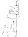
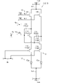
- FIG. 37 is a diagram schematically showing the circuit configuration of the sub-pixel portion 915 according to a reference example.
- Each sub-pixel portion 915 has, for example, a light emitting element 914 and a light emission control portion 922 that controls light emission, non-light emission, light emission intensity, and the like of the light emitting element 914 .
- the light emitting element 914 for example, a micro light emitting diode (LED) element or an organic electroluminescence (EL) element is applied.
- the light emitting element 914 is located on an insulating layer disposed on a first surface of a substrate, such as a glass plate, for example.
- the light emitting element 914 is electrically connected to the light emission control section 922 and the cathode potential input line 917 via, for example, through conductors arranged in through holes penetrating the insulating layer arranged in the pixel section.
- the positive electrode of the light emitting element 914 is connected to the anode potential input line 916 via the light emission control section 922 .
- the negative electrode of light emitting element 914 is connected to cathode potential input line 917 .
- the light emission control section 922 has, for example, a first transistor 912, a second transistor 913, a capacitive element 918, and a third transistor 919.
- the first transistor 912 functions as a switch for inputting an image signal to the sub-pixel portion 915, for example.
- a P-channel thin film transistor also referred to as a P-channel transistor
- a gate electrode of the first transistor 912 is connected to the scanning signal line 902, for example.
- a source electrode of the first transistor 912 is connected to the image signal line 903, for example.
- the drain electrode of the first transistor 912 is connected to the gate electrode of the second transistor 913, for example.
- the first transistor 912 switches between the source electrode and the drain electrode. It is in a conducting state (also called an on state or a closed state as a switch) in which current can flow between them.
- an image signal from the image signal line 903 is applied to the gate electrode of the second transistor 913 via the first transistor 912 .
- the second transistor 913 has, for example, a potential difference between the anode potential Vdd applied by the anode potential input line 916 and the cathode potential Vss applied by the cathode potential input line 917, and the level (potential) of the image signal transmitted from the image signal line 903. ) and functions as an element (also referred to as a driving element) that drives the light emitting element 914 with current.
- the anode potential input line 916 is connected to, for example, a first power line Lvd as a power line on the anode potential side.
- the anode potential Vdd applied from the first power supply line Lvd to the anode potential input line 916 is, for example, about 3 volts (V) to 5V.
- the cathode potential input line 917 is connected to, for example, a second power line Lvs as a power line on the cathode potential side.
- the cathode potential Vss applied from the second power supply line Lvs to the cathode potential input line 917 is, for example, about -3V to 0V.
- the second power line Lvs may be, for example, a grounded ground line.
- a P-channel transistor, for example, is applied to the second transistor 913 .
- the source electrode of the second transistor 913 is connected to the anode potential input line 916 .
- the drain electrode of the second transistor 913 is connected to the cathode potential input line 917 via the third transistor 919 and the light emitting element 914 .
- the second transistor 913 becomes conductive.
- the capacitive element 918 is arranged, for example, on a connection line connecting the gate electrode and the source electrode of the second transistor 913 .
- the capacitor 918 is, for example, a holding capacitor that holds the potential of an image signal input to the gate electrode of the second transistor 913 for a period (also referred to as one frame period) until the next image signal is input (also referred to as rewriting). function as
- the third transistor 919 is arranged, for example, on the drive line 925 between the second transistor 913 and the light emitting element 914, and can control light emission and non-light emission of the light emitting element 914.
- a P-channel transistor for example, is applied to the third transistor 919 .
- the source electrode of the third transistor 919 is connected to the drain electrode of the second transistor 913 and the drain electrode of the third transistor 919 is connected to the positive electrode of the light emitting element 914 .
- an L signal as a light emission control signal also referred to as an Emi signal
- the third transistor 919 is turned on.
- current also referred to as driving current
- the intensity (luminance) of light emitted from the light emitting element 914 can be controlled by controlling the level (potential) of the image signal.
- the drive current does not sufficiently flow through the light-emitting element 914, and the light-emitting element 914 may not emit light with the desired intensity.
- the light-emitting element 914 emits light at a desired intensity. Failure to do so may result in poor lighting.
- FIG. 38 is a diagram schematically showing the circuit configuration of the sub-pixel portion 915 according to another reference example.
- the circuit configuration of the sub-pixel portion 915 shown in FIG. 38 is based on the circuit configuration of the sub-pixel portion 915 in FIG. 37 described above, with some configurations replaced with other configurations and additional configurations added. It is a thing.
- part of the circuit configuration of the sub-pixel portion 915 in FIG. Of the circuit configuration of the sub-pixel portion 915 shown in FIG.
- the additional configuration in the circuit configuration of the sub-pixel portion 915 shown in FIG. 38 is the switching control portion 927 .
- the first drive line 925a and the second drive line 925b are connected to the light emission control section 922 and connected in parallel.
- one drive line 925 is a normal drive line (also referred to as a normal drive line)
- the other drive line 925 is a preliminary drive line. (also called a redundant drive line).
- the first drive line 925 a is connected to the positive electrode of the first light emitting element 914 a and the negative electrode of the first light emitting element 914 a is connected to the cathode potential input line 917 .
- the second drive line 925b is connected to the positive electrode of the second light emitting element 914b, and the negative electrode of the second light emitting element 914b is connected to the cathode potential input line 917.
- the first switch 926a is arranged, for example, on the first drive line 925a, and can set the first drive line 925a to a use state (also referred to as a drive state) or a non-use state (also referred to as a non-drive state). can.
- the second switch 926b is arranged, for example, on the second drive line 925b, and can set the second drive line 925b to a use state (drive state) or a non-use state (non-drive state).
- the switching control unit 927 sets one of the first switch 926a and the second switch 926b to a non-conducting state (also referred to as an OFF state or an open state as a switch) in which current cannot flow, and switches the other switch.
- a non-conducting state also referred to as an OFF state or an open state as a switch
- the switch sets the switch to the conducting state.
- one of the first light emitting element 914a and the second light emitting element 914b as the two light emitting elements 914, which is not defective can always emit light.
- P-channel transistors are applied to the first switch 926a and the second switch 926b.
- the switching control unit 927 inputs an ON signal (Vga: L signal) to the gate electrode of the first switch 926a and the second switch 926b.
- An off signal (Vgb: H signal) is input to the gate electrode of .
- the switching control section 927 inputs an off signal (Vga: H signal) to the gate electrode of the first switch 926a and switches the gate electrode of the second switch 926b. to input an on signal (Vgb: L signal).
- the characteristics of the light emitting element 914 can include, for example, internal resistance and luminous efficiency.
- the characteristics of the second transistor 913 can include, for example, the voltage required for driving in the saturation region (also called saturation operating voltage).
- the usage conditions related to the light emission of the light emitting element 914 can include, for example, setting values of upper and lower limits of the driving current, forward voltage, luminance, etc., of the light emitting element 914 .
- the internal resistance may be different for each light emitting element 914 even if the light emitting elements 914 emit the same color.
- luminous efficiency in general, the luminous efficiency of the light emitting element 914 that emits red light (wavelength of about 640 nm to 770 nm) tends to be relatively low, and the luminous efficiency of the light emitting element 914 that emits green light (wavelength of about 490 nm to 550 nm) is relatively low. And the light emitting element 914 that emits blue light (with a wavelength of about 430 nm to 490 nm) tends to have relatively high light emission efficiency.
- the luminance of the light emitting element 914 emitting red light tends to be low, and the luminance of the light emitting element 914 emitting green light and the light emitting element 914 emitting blue light tends to increase.
- the drive current is about 1/2 of that when one of them is caused to emit light.
- the driving current is about half of that when one of them is caused to emit light.
- the forward voltage of the light emitting element 914 that emits red light tends to be relatively large, and the forward voltage of the light emitting element 914 that emits green light and the light emitting element 914 that emits blue light tends to be relatively small.
- the forward voltage is, for example, when two light emitting elements 914 are connected in parallel and both of them emit light (referred to as parallel two light emitting type), and when two light emitting elements 914 are connected in parallel and one of them emits light. (referred to as parallel one-emission type), the parallel one-emission type has a relatively larger forward voltage.
- the drive current flowing through one light-emitting element 914 is about half that of the parallel one-emission type, so the forward voltage is relatively small.
- the power consumption of the light emitting element 914 is relatively large in the parallel 1 light emission type, so the power consumption of the driving thin film transistor is relatively small. Therefore, the power efficiency of the driving thin film transistor is improved in the parallel single light emission type.
- the anode potential Vdd and the cathode potential are the same when the light-emitting element 914 emits light.
- the forward voltage Vf applied to the light emitting element 914 may increase.
- at least one of the internal resistance, the upper limit setting value of the driving current, the upper limit setting value of the forward voltage, and the upper limit setting value of the luminance is large in the light emitting element 914.
- the forward voltage Vf applied to the light-emitting element 914 can become large even when the light-emitting element 914 has low light-emitting efficiency.
- the voltage Vf that accounts for the potential difference (Vdd ⁇ Vss) increases, for example, the voltage Vds between the drain electrode and the source electrode (also referred to as the drain-source voltage) of the second transistor 913 decreases.
- a drop in the anode potential Vdd according to the distance between the power supply and the portion of the first power supply line Lvd to which the anode potential input line 916 is connected, or the cathode potential input line of the second power supply line Lvs.
- the potential difference between the anode potential Vdd and the cathode potential Vss may decrease due to the increase in the cathode potential Vss according to the distance between the point where the 917 is connected and the power supply. Therefore, for example, as the potential difference between the anode potential Vdd and the cathode potential Vss decreases, the conditions for driving the second transistor 913 in the saturation region become severe. That is, it becomes difficult to drive the second transistor 913 in the saturation region. As a result, for example, when the display device is viewed from above, gradation (also referred to as luminance unevenness) in which the luminance gradually decreases is likely to occur. As a result, for example, the image quality on the display may be degraded.
- the saturation operating voltage of the second transistor 913 is high in any one of the sub-pixel units 915 among the plurality of sub-pixel units 915, the potential difference between the anode potential Vdd and the cathode potential Vss decreases. Therefore, the conditions for driving the second transistor 913 in the saturation region become severe. As a result, for example, luminance unevenness is likely to occur in the display device. As a result, for example, the image quality on the display may be degraded.
- any sub-pixel portion 915 of the plurality of sub-pixel portions 915 in the pixel portion depending on at least one of the characteristics of the light-emitting element 914 and the usage conditions related to light emission, when the light-emitting element 914 emits light, the light-emitting element 914 can cause a large current to flow through
- the sub-pixel portion 915 in the light-emitting element 914, at least one of the upper limit setting value of the driving current, the upper limit setting value of the forward voltage, and the upper limit setting value of the luminance is large.
- the current flowing through the light emitting element 914 can be large.
- the light-emitting element 914 is likely to deteriorate over time due to heat generated by a large amount of current flowing through the light-emitting element 914, and the image quality of the display device may be degraded.
- the light emitting element 914 is likely to deteriorate over time due to heat generation or the like, and the image quality of the display device may deteriorate.
- the light emitting element 914 emits light.
- the forward voltage Vf applied to 914 may decrease, and the drain-source voltage Vds of the second transistor 913 may increase.
- at least one of the internal resistance, the lower limit setting value of the driving current, the lower limit setting value of the forward voltage, and the lower limit setting value of the luminance is small.
- the forward voltage Vf applied to the light emitting element 914 may be small, and the drain-source voltage Vds of the second transistor 913 may be large.
- the power consumption of the second transistor 913 is large, and the energy efficiency of the sub-pixel portion 915 may decrease. As a result, for example, power consumption in the display device may increase.
- a pixel portion circuit for example, a display panel having the pixel circuit, a display device having the pixel circuit, and a composite display device having a plurality of the display devices, a plurality of sub-pixel portion circuits
- a display panel having the pixel circuit for example, a display panel having the pixel circuit, a display device having the pixel circuit, and a composite display device having a plurality of the display devices, a plurality of sub-pixel portion circuits
- pixel circuits, display panels, display devices, and composite display devices may have different characteristics when at least one of the characteristics of the elements and the usage conditions of the light-emitting elements are different among the plurality of sub-pixel circuits. , created a technology that can improve the performance of display devices.
- FIG. 1 is a front view schematically showing an example of the display device 100 according to the first embodiment.
- FIG. 2 is a back view schematically showing an example of the display device 100 according to the first embodiment.
- FIG. 3 is a block circuit diagram schematically showing an example of the configuration of the display device 100 according to the first embodiment.
- the display device 100 includes, for example, a display panel 100p and a driving section 30.
- the display panel 100p includes a plurality of pixel circuits 10, for example.
- the display panel 100p is, for example, flat.
- the display panel 100p includes, for example, a substrate 20 and a plurality of pixel circuits 10.
- FIG. 1 is a front view schematically showing an example of the display device 100 according to the first embodiment.
- FIG. 2 is a back view schematically showing an example of the display device 100 according to the first embodiment.
- FIG. 3 is a block circuit diagram schematically showing an example of the configuration of the display device 100 according to the first embodiment.
- the display device 100
- the substrate 20 has, for example, a first surface (also referred to as a first main surface) F1, a second surface (also referred to as a second main surface) F2, and a plurality of side surfaces F3.
- the second surface F2 is a surface opposite to the first surface F1.
- the plurality of side faces F3 connect the first face F1 and the second face F2, respectively.
- a flat substrate for example, is applied to the substrate 20 .
- the multiple side faces F3 include a first side face F31, a second side face F32, a third side face F33, and a fourth side face F34.
- the first side surface F31 connects the first side of the first surface F1 and the first side of the second surface F2. In other words, the first side surface F31 has the first side of the first surface F1 and the first side of the second surface F2 as two opposite sides.
- the second side surface F32 connects the second side of the first surface F1 and the second side of the second surface F2. In other words, the second side surface F32 has the second side of the first surface F1 and the second side of the second surface F2 as two opposite sides.
- the third side surface F33 connects the third side of the first surface F1 and the third side of the second surface F2. In other words, the third side surface F33 has the third side of the first surface F1 and the third side of the second surface F2 as two opposing sides.
- the fourth side surface F34 connects the fourth side of the first surface F1 and the fourth side of the second surface F2.
- the fourth side surface F34 has the fourth side of the first surface F1 and the fourth side of the second surface F2 as two opposite sides.
- the first surface F1 is a flat surface along the XZ plane and faces the -Y direction.
- the second surface F2 is a flat surface along the XZ plane and faces the +Y direction.
- the first side surface F31 faces the +Z direction.
- the second side face F32 faces the -X direction.
- the third side surface F33 faces the -Z direction.
- the fourth side surface F34 faces the +X direction.
- a glass plate for example, is applied to the substrate 20 .
- the glass plate may or may not be transparent.
- the substrate 20 is, for example, a colored glass substrate, a frosted glass substrate, a plastic substrate, a ceramic substrate, a metal substrate, or a composite substrate in which two or more of these substrates are laminated. may apply.
- the plurality of pixel circuits 10 are circuits that respectively constitute a pixel section.
- the plurality of pixel circuits 10 are arranged in a matrix, for example.
- the plurality of pixel circuits 10 are arranged in a matrix on the first surface F1 of the substrate 20, for example.
- a plurality of pixel circuits 10 constitute one column of pixel circuits 10
- a plurality of pixel circuits 10 constitute one row of pixel circuits 10 .
- pixel circuits 10 of n rows ⁇ m columns (n and m are natural numbers) are arranged.
- the plurality of pixel circuits 10 constitute, for example, a portion (also referred to as an image display portion) 300 that displays an image.
- the image display unit 300 is positioned, for example, on the first surface F1 side of the substrate 20 .
- the image display unit 300 is positioned, for example, so as to cover substantially the entire surface of the first surface F1.
- the display device 100 has a structure in which the image display unit 300 is arranged on the entire surface of the first surface F1 side of the substrate 20 (also referred to as a frameless structure) or a structure around the image display unit 300. It has a structure in which the frame portion of the frame is as narrow as possible (also called a narrow frame structure).
- Each of the plurality of pixel circuits 10 has, for example, a plurality of sub-pixel circuits.
- the plurality of sub-pixel circuits are circuits forming sub-pixel portions included in the pixel portion.
- the multiple sub-pixel circuits include, for example, a first sub-pixel circuit 1, a second sub-pixel circuit 2, and a third sub-pixel circuit 3.
- the first sub-pixel circuit 1 can emit light of a first color, for example.
- the second sub-pixel circuit 2 can emit light of a second color different from the first color, for example.
- the third sub-pixel circuit 3 can, for example, emit light of a third color different from the first and second colors. For example, red, green and blue are applied to the first, second and third colors.
- each pixel circuit 10 for example, a first subpixel circuit 1, a second subpixel circuit 2, and a third subpixel circuit 3 are arranged in order in the row direction.
- a plurality of first subpixel circuits 1 constitute one row of first subpixel circuits 1, and a plurality of second subpixel circuits 2 constitute one row of second subpixel circuits 2.
- a plurality of third sub-pixel circuits 3 constitute one row of third sub-pixel circuits 3 .
- a plurality of first sub-pixel circuits 1 constitute one column of first sub-pixel circuits 1
- a plurality of second sub-pixel circuits 2 constitute one column of second sub-pixel circuits 2
- a plurality of The third sub-pixel circuits 3 constitute one column of the third sub-pixel circuits 3 .
- the first subpixel circuit 1, the second subpixel circuit 2, and the third subpixel circuit 3 may be arranged in any order.
- the drive unit 30 is electrically connected to, for example, a plurality of pixel circuits 10.
- the drive unit 30 is positioned, for example, on the second surface F2 side of the substrate 20 .
- a driving element such as an integrated circuit (IC) or a large-scale integration (LSI) is mounted on the substrate 20 in a chip-on-glass (COG) method. It can be formed by being mounted on the surface F2.
- the driving unit 30 may be, for example, a circuit board on which driving elements are mounted.
- the driving unit 30 includes low temperature polysilicon (Low Temperature Poly Silicon) directly formed on the second surface F2 of the substrate 20 by a thin film formation method such as a chemical vapor deposition (CVD) method.
- CVD chemical vapor deposition
- a thin film circuit (also referred to as a thin film circuit) including a thin film transistor (TFT) having a semiconductor layer of LTPS) may be used.
- the drive unit 30 includes, for example, wiring (also referred to as back surface wiring) W2 located on the second surface F2 of the substrate 20 and wiring (also referred to as side surface wiring) W3 located on the side surface F3 of the substrate 20. , are electrically connected to the image display section 300 located on the first surface F1 side of the substrate 20.
- FIG. Therefore, a plurality of wirings are included in, for example, the display panel 100p.
- the display panel 100p includes, for example, as shown in FIG. 3, a plurality of image signal lines 4s, a plurality of scanning signal lines (also referred to as gate signal lines) 4g, and a plurality of emission control signal lines 4e. I have.
- the plurality of scanning signal lines 4g and the plurality of image signal lines 4s are positioned, for example, in a grid pattern.
- the display panel 100p also includes, for example, a scanning signal line driving section 30g and a light emission control signal line driving section 30e.
- Each of the plurality of image signal lines 4s sends a signal (also referred to as an image signal) for controlling the degree of light emission to, for example, the first subpixel circuit 1, the second subpixel circuit 2, and the third subpixel circuit 3. can be transmitted.
- the image signal line 4s is positioned along one column of pixel circuits 10, for example. In the example of FIG. 3, three image signal lines 4s are positioned along one column of pixel circuits 10 .
- the three image signal lines 4s are, for example, a first image signal line (also referred to as a first image signal line) 4s1, a second image signal line (also referred to as a second image signal line) 4s2, and a third image signal line 4s1.
- an image signal line 4s3 positioned along the third sub-pixel circuit 3 of one column.
- the first image signal line 4s1 is electrically connected to each of the plurality of first sub-pixel circuits 1 forming one column
- the second image signal line 4s2 is It is electrically connected to each of the second sub-pixel circuits 2 forming one column
- the third image signal line 4s3 is electrically connected to each of the third sub-pixel circuits 3 forming one column.
- an image signal may be supplied from the drive unit 30 to each of the plurality of image signal lines 4s.
- the drive unit 30 may supply image signals to the plurality of image signal lines 4s via a selector circuit or the like.
- one selector circuit is arranged for the pixel circuits 10 of each column, and the image signal supplied from the driving unit 30 to the selector circuit is transferred to the first image signal line 4s1 and the second image signal line 4s1 by the selector circuit.
- 4s2 and the third image signal line 4s3 may be supplied time-sequentially (line-sequentially).
- a configuration having, for example, three transfer gate elements is applied to the selector circuit.
- the selector circuit may be arranged, for example, in an empty area of the image display section 300 on the first surface F1 of the substrate 20, or may be arranged in a frame portion outside the image display section 300.
- Each of the plurality of scanning signal lines 4g is, for example, a signal (scanning signal ) can be transmitted.
- One scanning signal line 4g is positioned along one row of pixel circuits 10, for example.
- the m-th scanning signal line 4g is positioned along the row of the pixel circuit 10 of the m-th row (m is a natural number).
- a signal line 4g is electrically connected.
- Scanning signals can be supplied to the plurality of scanning signal lines 4g in a time-sequential manner (line-sequential manner) from a scanning signal line driving section 30g, for example.
- Various circuits such as a shift register are applied to the scanning signal line driving unit 30g, for example.
- the scanning signal line driving section 30g is located on the first surface F1 of the substrate 20, for example. In this case, the scanning signal line driving section 30g may be arranged, for example, in an empty area of the image display section 300, or may be arranged in a frame portion outside the image display section 300.
- the scanning signal line driving section 30g can supply scanning signals to the plurality of scanning signal lines 4g time-sequentially (line-sequentially) in response to signals from the driving section 30, for example.
- the emission control signal line 4e transmits, for example, a signal for controlling emission timing (also referred to as emission control signal) to each of the first subpixel circuit 1, the second subpixel circuit 2, and the third subpixel circuit 3. be able to.
- One emission control signal line 4e is positioned along one row of pixel circuits 10, for example.
- the m-th emission control signal line 4e is positioned along the m-th row (m is a natural number) of the pixel circuits 10 .
- each of the plurality of first sub-pixel circuits 1, the plurality of second sub-pixel circuits 2, and the plurality of third sub-pixel circuits 3 included in the pixel circuit 10 of the m-th row emits light for the m-th line.
- a control signal line 4e is electrically connected.
- the light emission control signal can be supplied to the plurality of light emission control signal lines 4e in time sequence (line sequence) from the light emission control signal line drive unit 30e.
- Various circuits such as a shift register are applied to the light emission control signal line driving section 30e, for example.
- the light emission control signal line driving section 30e is located on the first surface F1 of the substrate 20, for example.
- the light emission control signal line driving section 30e may be arranged, for example, in an empty area of the image display section 300, or may be arranged in a frame portion outside the image display section 300.
- the light emission control signal line driving section 30e can, for example, respond to a signal from the driving section 30 and supply light emission control signals to the plurality of light emission control signal lines 4e in time sequence (line sequence).
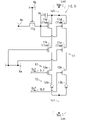
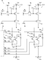
- FIG. 4 is a circuit diagram showing an example of the pixel circuit 10 according to the first embodiment.
- the pixel circuit 10 includes, for example, a first sub-pixel circuit 1 and a second sub-pixel circuit 2.
- the third subpixel circuit 3 has the same configuration as either the first subpixel circuit 1 or the second subpixel circuit 2, for example. Therefore, illustration of the third sub-pixel circuit 3 is omitted for the sake of convenience.
- the first sub-pixel circuit 1 has, for example, a first light emitting portion (also referred to as a first light emitting portion) 12 and a first setting portion (also referred to as a first setting portion) 13 . Also, the first sub-pixel circuit 1 has, for example, a first light emission control section (also referred to as a first light emission control section) 11 .
- the first light emitting unit 12 includes, for example, a first light emitting element 12a and a second light emitting element 12b.
- Each of the first light emitting element 12a and the second light emitting element 12b can emit light of a first color (eg, red light).
- a first color eg, red light
- the same light emitting element is applied to the first light emitting element 12a and the second light emitting element 12b.
- a micro light emitting diode (LED) element or an organic electroluminescence (EL) element is applied for example.
- the first light emitting element 12a and the second light emitting element 12b for example, a micro LED element or an organic EL element that emits light of a first color is applied.
- the first light emitting element 12a and the second light emitting element 12b are connected in parallel.
- the first light emitting element 12a and the second light emitting element 12b are located on an insulating layer arranged on the first surface F1 of the substrate 20, for example.
- the first light-emitting element 12a and the second light-emitting element 12b are electrically connected to other components of the first sub-pixel circuit 1, for example, via through conductors such as through holes penetrating the insulating layer. .
- the first light emitting unit 12 has a first power line as a power line on the anode potential side through the first setting unit 13, the first light emission control unit 11, and the first anode potential input line 1dl. Connected to Lvd. More specifically, for example, the positive electrode as the first electrode of each of the first light emitting element 12a and the second light emitting element 12b is connected to the first setting section 13, the first light emission control section 11 and the first anode potential input line. 1dl to the first power supply line Lvd.
- the first power line Lvd is connected to, for example, a power supply that applies an anode potential to the first power line Lvd.
- the first light emitting unit 12 is connected to, for example, a second power line Lvs as a power line on the cathode potential side via a first cathode potential input line 1sl. More specifically, for example, the negative electrode as the second electrode of each of the first light emitting element 12a and the second light emitting element 12b is connected to the second power supply line Lvs via the first cathode potential input line 1sl. There is The second power line Lvs is connected to, for example, a power supply that applies a cathode potential to the second power line Lvs.
- the first light emission control unit 11 can control light emission in the first light emission unit 12, for example. More specifically, the first light emission control unit 11 can control, for example, light emission, non-light emission, and light emission intensity of the first light emitting element 12a and the second light emitting element 12b.
- the first light emission control unit 11 has, for example, a first transistor 11g, a second transistor 11d, a first capacitive element 11c, and a third transistor 11e.
- the first transistor 11g functions, for example, as a switch element for inputting an image signal into the first light emission control section 11.
- a P-channel type thin film transistor (P-channel transistor) or the like is applied to the first transistor 11g.
- the gate electrode of the first transistor 11g is connected to the scanning signal line 4g.
- the source electrode of the first transistor 11g is connected to the first image signal line 4s1.
- the drain electrode of the first transistor 11g is connected to the gate electrode of the second transistor 11d.
- the first transistor 11g when an ON signal (here, a Low (L) signal) as a scanning signal from the scanning signal line 4g is input to the gate electrode of the first transistor 11g, the first transistor 11g has a source electrode and a drain electrode. It becomes a conducting state in which current can flow between As a result, for example, an image signal from the first image signal line 4s1 is applied to the gate electrode of the second transistor 11d via the first transistor 11g.
- an ON signal here, a Low (L) signal
- the second transistor 11d receives, for example, the potential difference between the anode potential Vdd given by the first anode potential input line 1dl and the cathode potential Vss given by the first cathode potential input line 1sl from the first image signal line 4s1. It functions as an element (also referred to as a drive element) that current-drives the first light emitting unit 12 according to the level (potential) of the image signal.
- the anode potential Vdd applied from the first power supply line Lvd to the first anode potential input line 1dl is, for example, about 3V to 5V.
- the cathode potential Vss applied from the second power supply line Lvs to the first cathode potential input line 1sl is, for example, about -3V to 0V.
- the second power line Lvs may be, for example, a grounded ground line.
- a P-channel transistor, for example, is applied to the second transistor 11d.
- the source electrode of the second transistor 11d is connected to the first anode potential input line 1dl.
- the drain electrode of the second transistor 11d is connected to the first cathode potential input line 1sl via the third transistor 11e, the first setting section 13 and the first light emitting section 12.
- the second transistor 11d becomes conductive so that a current can flow between the source electrode and the drain electrode. state.
- a driving current can flow from the first anode potential input line 1dl to the first light emitting section 12 via the second transistor 11d, the third transistor 11e, and the first setting section 13.
- the intensity (luminance) of light emission of the first light emitting unit 12 can be controlled according to the level (potential) of the image signal, for example.
- the second transistor 11d can control the light emission intensity of the first light emitting section 12, for example. From another point of view, the second transistor 11d can control the light emission intensity of the first light emitting element 12a and the second light emitting element 12b of the first light emitting section 12, for example.
- the first capacitive element 11c is positioned, for example, on a connection line connecting the gate electrode and the source electrode of the second transistor 11d.
- the first capacitive element 11c serves as a holding capacitor that holds the potential Vsig of the image signal input to the gate electrode of the second transistor 11d for a period (one frame period) until the next image signal is input (rewritten). Function.
- the third transistor 11e functions as a switch element for controlling light emission and non-light emission of the first light emitting section 12, for example.
- the third transistor 11e is located, for example, on a connection line (also referred to as a first drive line) that connects the second transistor 11d and the first light emitting section 12 .
- a P-channel transistor for example, is applied to the third transistor 11e.
- the source electrode of the third transistor 11e is connected to the drain electrode of the second transistor 11d. 12 is connected. More specifically, for example, the drain electrode of the third transistor 11e is connected through the first setting portion 13 to the positive electrodes of the first light emitting element 12a and the second light emitting element 12b.
- the gate electrode of the third transistor 11e is connected to the light emission control signal line 4e.
- an ON signal here, L signal
- the third transistor 11e is switched between the source electrode and the drain electrode.
- a conductive state is established in which a current can flow between them.
- a driving current flows from the first anode potential input line 1dl to the first light emitting section 12 via the second transistor 11d and the third transistor 11e, and the first light emitting section 12 can emit light.
- the first setting unit 13 sets, for each of the first light emitting element 12a and the second light emitting element 12b, a state in which light can be emitted (also referred to as a light-emitting state) and a state in which light cannot be emitted (also referred to as a non-light-emitting state). ) can be selectively set to either state.
- the light-emitting state is, for example, a state in which the light-emitting element can emit light according to the potential difference between the anode potential Vdd of the first power supply line Lvd and the cathode potential Vss of the second power supply line Lvs. To tell.
- the non-light-emitting state is, for example, a state in which the light-emitting element cannot emit light according to the potential difference between the anode potential Vdd of the first power supply line Lvd and the cathode potential Vss of the second power supply line Lvs.
- the first setting unit 13 causes the first light emitting element 12a and the second light emitting element 12b to emit light in response to a signal (also referred to as a setting control signal) from a setting control unit 5 configured by various circuits. It can be set to either one of an enabled state and a non-light emitting state.
- the setting control section 5 can output a setting control signal to the first setting section 13, for example.
- the setting control section 5 may be a control circuit section included in the driving section 30 .
- the setting control unit 5 also includes program software stored in the RAM (Random Access Memory) and ROM (Read Only Memory) of the drive element such as an IC (Integrated Circuit) or an LSI (Large Scale Integrated Circuit) included in the drive unit 30. It may be a functional configuration realized by Further, the setting control section 5 may be a functional configuration realized by program software stored in the RAM and ROM of the driving element separate from the driving section 30 . Also, the setting control section 5 may be a control circuit formed on a circuit board separate from the driving section 30 .
- the display device 100 includes a substrate 20 having a display surface (first surface F1), an anti-display surface (second surface F2) opposite to the display surface, and a side surface F3 connecting the display surface and the anti-display surface.
- the plurality of pixel circuits 10 are positioned on the display surface side of the substrate 20, and the driving section 30 is positioned on the opposite side of the display surface of the substrate 20.
- the frame portion (non-display portion) of the display surface can be narrowed or the frame portion can be eliminated.
- the drive unit 30 may be a drive element such as an IC or LSI, or may be a circuit board such as a flexible printed circuit (FPC) on which the drive element is mounted.
- the circuit board may be located on the opposite display side of the substrate 20 .
- the connection electrodes on this circuit board may be connected to the connection terminals on the opposite display surface of the substrate 20 .
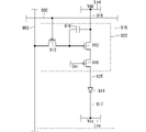
- the first setting unit 13 includes, for example, a fourth transistor 13a as a first switch and a fifth transistor 13b as a second switch.
- the fourth transistor 13a as the first switch can selectively set the first light emitting element 12a to either the light emitting state or the non-light emitting state.
- the fourth transistor 13a is connected in series with the first light emitting element 12a.
- a P-channel transistor for example, is applied to the fourth transistor 13a.
- the source electrode of the fourth transistor 13a is connected to the drain electrode of the third transistor 11e, and the drain electrode of the fourth transistor 13a is connected to the positive electrode of the first light emitting element 12a.
- the gate electrode of the fourth transistor 13a is connected to the setting control section 5 via a signal line (also referred to as a first setting control signal line) SL1.
- the setting control section 5 can output the first setting control signal Se1 to the gate electrode of the fourth transistor 13a, for example.
- the setting control unit 5 selects, for example, one of the first signal (L signal here) and the second signal (High (H) signal here) as the first setting control signal Se1.
- the first signal is an ON signal that makes the transistor gate-drain conductive
- the second signal is an OFF signal that makes the transistor gate-drain non-conductive.
- the first signal is a signal for setting the light-emitting element to a light-emitting state
- the second signal is a signal for setting the light-emitting element to a non-light-emitting state.
- the fourth transistor 13a when the L signal, which is the first signal, is input to the gate electrode of the fourth transistor 13a as the first setting control signal Se1 from the setting control unit 5, the fourth transistor 13a is placed between the source electrode and the drain electrode. It becomes a conductive state in which current can flow. As a result, for example, the first light emitting element 12a is set to a light emitting state. Further, for example, when the H signal, which is the second signal, is input to the gate electrode of the fourth transistor 13a as the first setting control signal Se1 from the setting control unit 5, the fourth transistor 13a operates with the source electrode and the drain electrode. It becomes a non-conducting state in which current cannot flow during Thereby, for example, the first light emitting element 12a is set to a non-light emitting state.
- the fifth transistor 13b as a second switch can selectively set the second light emitting element 12b to either a light emitting state or a non-light emitting state.
- the fifth transistor 13b for example, is connected in series with the second light emitting element 12b.
- a P-channel transistor for example, is applied to the fifth transistor 13b.
- the source electrode of the fifth transistor 13b is connected to the drain electrode of the third transistor 11e, and the drain electrode of the fifth transistor 13b is connected to the positive electrode of the second light emitting element 12b.
- the gate electrode of the fifth transistor 13b is connected to the setting control section 5 via a signal line (also referred to as a second setting control signal line) SL2.
- the setting control section 5 can output the second setting control signal Se2 to the gate electrode of the fifth transistor 13b, for example.
- the setting control section 5 can selectively output either one of the L signal as the first signal and the H signal as the second signal as the second setting control signal Se2.
- the fifth transistor 13b when the L signal, which is the first signal, is input to the gate electrode of the fifth transistor 13b as the second setting control signal Se2 from the setting control unit 5, the fifth transistor 13b is placed between the source electrode and the drain electrode. It becomes a conductive state in which current can flow. As a result, for example, the second light emitting element 12b is set to a light emitting state. Further, for example, when the H signal, which is the second signal as the second setting control signal Se2 from the setting control unit 5, is input to the gate electrode of the fifth transistor 13b, the fifth transistor 13b operates with the source electrode and the drain electrode. It becomes a non-conducting state in which current cannot flow during Thereby, for example, the second light emitting element 12b is set to a non-light emitting state.
- the first setting unit 13 turns on both the fourth transistor 13a as the first switch and the fifth transistor 13b as the second switch. Both the first light emitting element 12a and the second light emitting element 12b can be set to the light emitting state.
- the fourth transistor 13a as the first switch may be arranged on the negative electrode side of the first light emitting element 12a.
- the positive electrode of the first light emitting element 12a is connected to the drain electrode of the third transistor 11e
- the negative electrode of the first light emitting element 12a is connected to the fourth transistor 13a as the first switch and the first transistor 13a. It is connected to the second power supply line Lvs via the cathode potential input line 1sl.
- the negative electrode of the first light emitting element 12a is connected to the source electrode of the fourth transistor 13a
- the drain electrode of the fourth transistor 13a is connected to the second cathode potential input line 1sl via the first cathode potential input line 1sl.
- the fifth transistor 13b as the second switch may be arranged on the negative electrode side of the second light emitting element 12b.
- the positive electrode of the second light emitting element 12b is connected to the drain electrode of the third transistor 11e
- the negative electrode of the second light emitting element 12b is connected to the fifth transistor 13b as the second switch and the first transistor 13b. It is connected to the second power supply line Lvs via the cathode potential input line 1sl.
- the negative electrode of the second light emitting element 12b is connected to the source electrode of the fifth transistor 13b, and the drain electrode of the fifth transistor 13b is connected to the second cathode potential input line 1sl via the first cathode potential input line 1sl. It is connected to the power line Lvs.
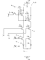
- the second sub-pixel circuit 2 has, for example, a second light emitting portion (also referred to as a second light emitting portion) 22 and a second setting portion (also referred to as a second setting portion) 23 .
- the second sub-pixel circuit 2 also has a second light emission control section (also referred to as a second light emission control section) 21, for example.
- the second light emitting section 22 includes, for example, a third light emitting element 22a and a fourth light emitting element 22b.
- Each of the third light emitting element 22a and the fourth light emitting element 22b can emit second color light (eg, green light or blue light).
- the same light emitting element is applied to the third light emitting element 22a and the fourth light emitting element 22b.
- a micro LED element or an organic EL element is applied to the third light emitting element 22a and the fourth light emitting element 22b. More specifically, for the third light emitting element 22a and the fourth light emitting element 22b, for example, a micro LED element or an EL element that emits light of the second color is applied.
- the third light emitting element 22a and the fourth light emitting element 22b are connected in parallel.
- the third light emitting element 22a and the fourth light emitting element 22b are located on an insulating layer arranged on the first surface F1 of the substrate 20, for example.
- the third light-emitting element 22a and the fourth light-emitting element 22b are electrically connected to other components of the second sub-pixel circuit 2, for example, through through conductors such as through holes penetrating the insulating layer.
- the second light emitting section 22 is connected to the first power line Lvd via the second setting section 23, the second light emission control section 21 and the second anode potential input line 2dl, for example.
- the positive electrode as the first electrode of each of the third light emitting element 22a and the fourth light emitting element 22b is connected to the second setting section 23, the second light emission control section 21 and the second anode potential input line. 2dl to the first power supply line Lvd.
- the second light emitting section 22 is connected to the second power supply line Lvs via the second cathode potential input line 2sl, for example.
- the negative electrodes as the second electrodes of the third light emitting element 22a and the fourth light emitting element 22b are connected to the second power supply line Lvs through the second cathode potential input line 2sl.
- the second light emission control section 21 can control light emission in the second light emitting section 22, for example. More specifically, the second light emission control unit 21 can control, for example, light emission, non-light emission, and light emission intensity of the third light emitting element 22a and the fourth light emitting element 22b.
- the second light emission control section 21 has, for example, the same configuration as the first light emission control section 11 .
- the second light emission control section 21 has, for example, a sixth transistor 21g, a seventh transistor 21d, a second capacitive element 21c, and an eighth transistor 21e.
- the sixth transistor 21g functions, for example, as a switch element for inputting an image signal into the second emission control section 21.
- a P-channel transistor for example, is applied to the sixth transistor 21g.
- the gate electrode of the sixth transistor 21g is connected to the scanning signal line 4g.
- the source electrode of the sixth transistor 21g is connected to the second image signal line 4s2.
- the drain electrode of the sixth transistor 21g is connected to the gate electrode of the seventh transistor 21d.
- an on-signal here, L signal
- the sixth transistor 21g is provided between the source electrode and the drain electrode. It becomes a conductive state through which current can flow.
- the image signal from the second image signal line 4s2 is applied to the gate electrode of the seventh transistor 21d via the sixth transistor 21g.
- the seventh transistor 21d receives, for example, the potential difference between the anode potential Vdd given by the second anode potential input line 2dl and the cathode potential Vss given by the second cathode potential input line 2sl from the second image signal line 4s2. It functions as an element (driving element) that current-drives the second light emitting unit 22 according to the level (potential) of the image signal.
- the anode potential Vdd applied from the first power supply line Lvd to the second anode potential input line 2dl is, for example, about 3V to 5V.
- the cathode potential Vss applied from the second power supply line Lvs to the second cathode potential input line 2sl is, for example, about -3V to 0V.
- a P-channel transistor for example, is applied to the seventh transistor 21d.
- the source electrode of the seventh transistor 21d is connected to the second anode potential input line 2dl.
- the drain electrode of the seventh transistor 21d is connected to the second cathode potential input line 2sl via the eighth transistor 21e, the second setting section 23 and the second light emitting section 22.
- the seventh transistor 21d becomes conductive so that a current can flow between the source electrode and the drain electrode. state.
- a driving current can flow from the second anode potential input line 2dl to the second light emitting section 22 via the seventh transistor 21d, the eighth transistor 21e, and the second setting section .
- the intensity (luminance) of light emission of the second light emitting unit 22 can be controlled, for example, according to the level (potential) of the image signal.
- the seventh transistor 21d can control the light emission intensity of the second light emitting section 22, for example. From another point of view, the seventh transistor 21d can control the light emission intensity of the third light emitting element 22a and the fourth light emitting element 22b of the second light emitting section 22, for example.
- the second capacitive element 21c is positioned, for example, on a connection line connecting the gate electrode and the source electrode of the seventh transistor 21d.
- the second capacitive element 21c serves as a holding capacitor that holds the potential Vsig of the image signal input to the gate electrode of the seventh transistor 21d for a period (a period of one frame) until the next image signal is input (rewritten). Function.
- the eighth transistor 21 e functions, for example, as a switch element for controlling light emission and non-light emission of the second light emitting section 22 .
- the eighth transistor 21e is located, for example, on a connection line (also referred to as a second drive line) that connects the seventh transistor 21d and the second light emitting section 22 .
- a P-channel transistor for example, is applied to the eighth transistor 21e.
- the source electrode of the eighth transistor 21e is connected to the drain electrode of the seventh transistor 21d, and the drain electrode of the eighth transistor 21e is connected to the second light emitting unit via the second setting unit 23. 22 is connected.
- the drain electrode of the eighth transistor 21e is connected to the positive electrodes of the third light emitting element 22a and the fourth light emitting element 22b via the second setting portion 23, respectively.
- the gate electrode of the eighth transistor 21e is connected to the light emission control signal line 4e.
- an ON signal here, L signal
- the eighth transistor 21e is switched between the source electrode and the drain electrode.
- a conductive state is established in which a current can flow between them.
- a driving current flows from the second anode potential input line 2dl to the second light emitting section 22 via the seventh transistor 21d and the eighth transistor 21e, and the second light emitting section 22 can emit light.
- the second setting unit 23 can selectively set each of the third light emitting element 22a and the fourth light emitting element 22b to either a light emitting state or a non-light emitting state.
- the second setting unit 23 switches each of the third light emitting element 22a and the fourth light emitting element 22b to either a light emitting state or a non-light emitting state according to a signal (setting control signal) from the setting control unit 5, for example. can be selectively set to either state.
- the setting control section 5 can output a setting control signal to the second setting section 23, for example.
- the second setting unit 23 includes, for example, a ninth transistor 23a as a third switch and a tenth transistor 23b as a fourth switch.
- the ninth transistor 23a as the third switch can, for example, selectively set the third light emitting element 22a to either a light emitting state or a non-light emitting state.
- the ninth transistor 23a for example, is connected in series with the third light emitting element 22a.
- a P-channel transistor for example, is applied to the ninth transistor 23a.
- the source electrode of the ninth transistor 23a is connected to the drain electrode of the eighth transistor 21e, and the drain electrode of the ninth transistor 23a is connected to the positive electrode of the third light emitting element 22a.
- the gate electrode of the ninth transistor 23a is connected to the setting control section 5 via a signal line (also referred to as a third setting control signal line) SL3.
- the setting control section 5 can, for example, output the third setting control signal Se3 to the gate electrode of the ninth transistor 23a.
- the setting control section 5 can selectively output either one of the L signal as the first signal and the H signal as the second signal as the third setting control signal Se3.
- the ninth transistor 23a when the L signal, which is the first signal, is input to the gate electrode of the ninth transistor 23a as the third setting control signal Se3 from the setting control unit 5, the ninth transistor 23a is placed between the source electrode and the drain electrode. It becomes a conductive state in which current can flow. As a result, for example, the third light emitting element 22a is set to a light emitting state. Further, for example, when the H signal, which is the second signal, is input to the gate electrode of the ninth transistor 23a as the third setting control signal Se3 from the setting control unit 5, the ninth transistor 23a operates with the source electrode and the drain electrode. It becomes a non-conducting state in which current cannot flow during Thereby, for example, the third light emitting element 22a is set to a non-light emitting state.
- the tenth transistor 23b as the fourth switch can selectively set the fourth light emitting element 22b to either a light emitting state or a non-light emitting state.
- the tenth transistor 23b for example, is connected in series with the fourth light emitting element 22b.
- a P-channel transistor for example, is applied to the tenth transistor 23b.
- the source electrode of the tenth transistor 23b is connected to the drain electrode of the eighth transistor 21e, and the drain electrode of the tenth transistor 23b is connected to the positive electrode of the fourth light emitting element 22b.
- the gate electrode of the tenth transistor 23b is connected to the setting control section 5 via a signal line (also referred to as a fourth setting control signal line) SL4.
- the setting control section 5 can output the fourth setting control signal Se4 to the gate electrode of the tenth transistor 23b, for example.
- the setting control section 5 can selectively output either one of the L signal as the first signal and the H signal as the second signal as the fourth setting control signal Se4.
- the tenth transistor 23b when the L signal, which is the first signal, is input to the gate electrode of the tenth transistor 23b as the fourth setting control signal Se4 from the setting control unit 5, the tenth transistor 23b is placed between the source electrode and the drain electrode. It becomes a conductive state in which current can flow. As a result, for example, the fourth light emitting element 22b is set to a light emitting state. Further, for example, when the H signal, which is the second signal as the fourth setting control signal Se4 from the setting control unit 5, is input to the gate electrode of the tenth transistor 23b, the tenth transistor 23b is configured to have a source electrode and a drain electrode. It becomes a non-conducting state in which current cannot flow during Thereby, for example, the fourth light emitting element 22b is set to a non-light emitting state.
- the second setting unit 23 selectively turns on either one of the ninth transistor 23a as the third switch and the tenth transistor 23b as the fourth switch. By doing so, either one of the third light emitting element 22a and the fourth light emitting element 22b can be selectively set to a light emitting state.
- the second setting unit 23 selects one of the ninth transistor 23a as the third switch and the tenth transistor 23b as the fourth switch. Either one of the third light-emitting element 22a and the fourth light-emitting element 22b can be selectively set to the non-light-emitting state.
- the ninth transistor 23a as the third switch may be arranged on the negative electrode side of the third light emitting element 22a.
- the positive electrode of the third light emitting element 22a is connected to the drain electrode of the eighth transistor 21e
- the negative electrode of the third light emitting element 22a is connected to the ninth transistor 23a and the second transistor 23a as the third switch. It is connected to the second power supply line Lvs through the cathode potential input line 2sl.
- the negative electrode of the third light emitting element 22a is connected to the source electrode of the ninth transistor 23a
- the drain electrode of the ninth transistor 23a is connected to the second cathode potential input line 2sl via the second cathode potential input line 2sl.
- the tenth transistor 23b as the fourth switch may be arranged on the negative electrode side of the fourth light emitting element 22b.
- the positive electrode of the fourth light emitting element 22b is connected to the drain electrode of the eighth transistor 21e
- the negative electrode of the fourth light emitting element 22b is connected to the tenth transistor 23b and the second transistor 23b as the fourth switch. It is connected to the second power supply line Lvs through the cathode potential input line 2sl.
- the negative electrode of the fourth light emitting element 22b is connected to the source electrode of the tenth transistor 23b, and the drain electrode of the tenth transistor 23b is connected to the second cathode potential input line 2sl via the second cathode potential input line 2sl. It is connected to the power line Lvs.
- FIG. 5 is a block diagram schematically showing an example of the configuration of the setting control section 5.
- the setting control section 5 has, for example, a plurality of signal output circuits 51 and a combination circuit 52 .
- the multiple signal output circuits 51 include, for example, a first signal output circuit (also referred to as a first signal output circuit) 511 and a second signal output circuit (also referred to as a second signal output circuit) 512 .
- Each signal output circuit 51 can, for example, selectively output one of the L signal, which is the first signal, and the H signal, which is the second signal, as the switching signal Si.
- the first signal output circuit 511 selectively outputs one of the L signal that is the first signal and the H signal that is the second signal as the first switching signal (also referred to as the first switching signal) Si0.
- the second signal output circuit 512 selectively outputs one of the L signal that is the first signal and the H signal that is the second signal as a second switching signal (also referred to as a second switching signal) Si1. be able to.
- Each signal output circuit 51 includes, for example, a flip-flop circuit, a latch circuit, or the like that can switch the switching signal Si to one of the L signal and the H signal and retain that state. circuit), or a circuit (also referred to as a fuse circuit) in which the switching signal Si switches between an L signal and an H signal in response to disconnection of a portion of the wiring.
- FIG. 6 is a circuit diagram showing a first example of the signal output circuit 51.
- each of the plurality of signal output circuits 51 may be applied with, for example, a holding circuit.
- the holding circuit as the signal output circuit 51 is, for example, once input (written) with a signal (also referred to as a setting signal) as data for setting the state, thereby outputting an L signal and an H signal as the switching signal Si. It is set to a state in which one of them continues to be output.
- the image signal line 4s is used as a signal line (also referred to as a setting signal write signal line) for inputting (writing) a setting signal to each signal output circuit 51, and the scanning signal line 4g is used for each signal output.
- the circuit 51 is used as a signal line (also referred to as a specified signal input signal line) for inputting a signal (also referred to as a specified signal) that specifies the timing of inputting (writing) a setting signal to the circuit 51 .
- one scanning signal line 4g may be connected to the first signal output circuit 511 and to the second signal output circuit 512 via a NOT circuit.
- a first timing at which a setting signal is input (written) from the image signal line 4s to the holding circuit as the first signal output circuit 511 by one scanning signal line 4g, and the image signal line A second timing at which the setting signal is input (written) to the holding circuit as the second signal output circuit 512 from 4s can be specified in time sequence.
- the L signal as the designation signal from the scanning signal line 4g is input to the holding circuit as the first signal output circuit 511, and the L signal as the designation signal from the scanning signal line 4g is a signal (non-designated signal) in the NOT circuit. is converted into an H signal (also referred to as a designated signal) and input to a holding circuit as a second signal output circuit 512 .
- H signal also referred to as a designated signal
- a setting signal may be input (written) to the holding circuit as the first signal output circuit 511 from the line 4s.
- the designated signal may be, for example, an H signal.
- the L signal or H signal as the setting signal is input (written) from the image signal line 4s at the timing when the designated signal is input from the scanning signal line 4g. .
- the L signal or H signal as the setting signal is input (written) from the image signal line 4s at the timing when the designated signal is input from the scanning signal line 4g. done.
- each of the plurality of pixel circuits 10 has the setting control unit 5
- the first image signal line 4s1 connected to the first subpixel circuit 1 the second subpixel
- Each of the second image signal line 4s2 connected to the circuit 2 and the third image signal line 4s3 connected to the third subpixel circuit 3 can be used as a setting signal write signal line.
- the scanning signal line 4g connected to the first subpixel circuit 1, the second subpixel circuit 2 and the third subpixel circuit 3 can be used as the designated signal input signal line.
- FIG. 7 is a circuit diagram showing a second example of the signal output circuit 51.
- a fuse circuit for example, is applied to each of the plurality of signal output circuits 51 .
- the fuse circuit as the signal output circuit 51 has, for example, a first circuit section 51C1, a second circuit section 51C2, a signal input section 51I, and a signal output section 51U.
- the signal input section 51I is a section to which a signal is input from the outside of the signal output circuit 51 .
- a signal is input to the signal input unit 51I from the drive unit 30 via a predetermined wiring, for example.
- CMOS NOT circuit as an inversion logic circuit is applied to the first circuit section 51C1.
- a CMOS NOT circuit for example, a P-channel transistor and an N-channel transistor are connected in series between a positive power supply line applying a positive potential VGH and a negative power supply line applying a negative potential VGL. ing.
- the negative potential VGL may be, for example, a reference potential (GND) or 0 volts.
- the source electrode of the P-channel transistor is connected to the positive power supply line
- the drain electrode of the P-channel transistor is connected to the drain electrode of the N-channel transistor
- the source electrode of the N-channel transistor is connected to the negative power line.
- the portion where the gate electrode of the P-channel transistor and the gate electrode of the N-channel transistor are connected is the input portion (also referred to as the first input portion).
- a portion connected to the drain electrode of the transistor is an output portion (also referred to as a first output portion).
- This CMOS type NOT circuit can invert the logic level of the voltage of the signal input to the first input section and output the signal from the first output section.
- a first input section of the CMOS NOT circuit is connected to the signal input section 51I.
- the first circuit section 51C1 when the L signal is input from the signal input section 51I to the first input section, the first circuit section 51C1 outputs the H signal from the first output section and outputs the H signal from the signal input section 51I to the first input section.
- an L signal can be output from the first output section.
- the first circuit section 51C1 also includes a specific wiring portion (also referred to as a specific wiring portion) 51P on the wiring that connects the source electrode of the N-channel transistor and the negative power supply line, for example.
- each signal output circuit 51 includes a specific wiring portion 51P.
- the specific wiring portion 51P is a portion to be cut, which will be described later.
- the specific wiring portion 51P is located on the insulating layer arranged on the first surface F1 of the substrate 20, the specific wiring portion 51P is fused by laser light irradiation, mechanically cut using a grinding device, or etched. It can be easily cleaved, such as by chemical cleavage using, for example. That is, the specific wiring portion 51P is a portion that can be fixed to either the conducting state or the non-conducting state (also referred to as the conducting/non-conducting fixed selection portion).
- the second circuit section 51C2 has, for example, a buffer circuit section 51B having two cascaded NOT gates N1 and N2, and a wiring section 51W connected in parallel with the buffer circuit section 51B.
- the second circuit section 51C2 includes, for example, an input section (also referred to as a second input section) connected to the first output section of the first circuit section 51C1 and an output section (also referred to as a second input section) connected to the signal output section 51U. (also referred to as a second output section).
- the buffer circuit portion 51B can stabilize and correct the voltage level of the signal input from the first output portion to the second input portion of the first circuit portion 51C1 and output the same.
- the second circuit unit 51C2 when an L signal is input from the first circuit unit 51C1 to the second input unit, the second circuit unit 51C2 outputs a stabilized and corrected L signal from the second output unit, When an H signal is input to the second input from the second output, a stabilized and corrected H signal can be output from the second output.
- the signal output circuit 51 As the signal output circuit 51 having the above configuration, it is assumed that an L signal is input to the signal input section 51I, for example. In this case, the first circuit section 51C1 inverts the L signal and outputs the H signal, and the second circuit section 51C2 outputs the stabilized and corrected H signal. As a result, the signal output unit 51U outputs the H signal as the switching signal Si to the combinational circuit 52 . Also, in the fuse circuit as the signal output circuit 51 having the above configuration, it is assumed that an H signal is input to the signal input section 51I, for example. In this case, the first circuit section 51C1 inverts the H signal and outputs the L signal, and the second circuit section 51C2 outputs the stabilized and corrected L signal. As a result, the signal output section 51U outputs an L signal as the switching signal Si to the combinational circuit 52 .
- the relationship between the signal input to the signal input section 51I and the signal output from the signal output section 51U is switched depending on whether or not the specific wiring portion 51P is disconnected. .
- the fuse circuit as the signal output circuit 51 is in a state in which the specific wiring portion 51P is not disconnected (also referred to as a non-disconnected state)
- the signal output portion 51U is switched to the signal output portion 51U.
- the H signal is input to the signal input section 51I
- the L signal is output from the signal output section 51U.
- the fuse circuit as the signal output circuit 51 is in a state in which the specific wiring portion 51P is disconnected (also referred to as a disconnected state), when an L signal is input to the signal input portion 51I, the signal output portion Even if the H signal is output from 51U and then the H signal is input to the signal input section 51I, the signal output from the signal output section 51U does not change. Therefore, for example, if the fuse circuit as the signal output circuit 51 is in a cut state, once an L signal is input to the signal input section 51I and an H signal is output from the signal output section 51U, Even if the H signal is input to the signal input section 51I, the signal output section 51U continues to output the H signal. At this time, for example, the signal output circuit 51 plays a role of storing the state in which the second circuit section 51C2 continues to output the H signal from the signal output section 51U.
- the relationship between the input and the output of the fuse circuit which changes depending on whether or not the specific wiring portion 51P is disconnected, is used to switch the switching signal Si output from the fuse circuit as the signal output circuit 51 to L. can be switched between the signal and the H signal.
- the switching signal Si output from the signal output section 51U becomes the H signal.
- the signal is output.
- the switching signal Si output from the unit 51U becomes an L signal.
- an L signal is input from the fuse circuit as the signal output circuit 51 in the uncut state to the combination circuit 52 as the switching signal Si.
- the switching signal Si output from the signal output section 51U is changed to H signal.
- the signal is output.
- the switching signal Si output from the unit 51U is maintained at the H signal.
- an H signal is input from the fuse circuit as the signal output circuit 51 in the disconnected state to the combination circuit 52 as the switching signal Si.
- the fuse circuit as the signal output circuit 51 changes the switching signal Si output to the combinational circuit 52 from the L signal of the first potential in response to disconnection of the specific wiring portion 51P. It can be set to the H signal of the second potential. If such a configuration is adopted, for example, the circuit scale of the signal output circuit 51 is less likely to increase.
- the combination circuit 52 can output a setting control signal according to a plurality of switching signals Si input from the plurality of signal output circuits 51, for example.
- the combination circuit 52 outputs the first setting control signal Se1, the second setting control signal Se1, and the second setting control signal Se1 according to the combination of the L signal and the H signal as the switching signals Si input from the plurality of signal output circuits 51, for example.
- an L signal that is the first signal or an H signal that is the second signal can be output.
- FIG. 8 is a truth table showing an example of the relationship between the switching signal Si input to the combination circuit 52, the setting control signal output from the combination circuit 52, and the light emitting elements set to the light emitting state.
- the combinational circuit 52 receives, for example, the inputs of the first switching signal Si0 and the second switching signal Si1, the first setting control signal Se1, the second setting control signal Se2, the third setting control signal Se3, and the fourth setting control signal.
- Various logic outputs are executed so that the output of the signal Se4 has the relationship shown in FIG. For example, as shown in FIG.
- the L signal as the first switching signal Si0 and the L signal as the second switching signal Si1 are input to the combination circuit 52, the L signal as the first setting control signal Se1 is input.
- An H signal is output.
- the first setting unit 13 turns on both the fourth transistor 13a as the first switch and the fifth transistor 13b as the second switch, so that the first light emitting element 12a and the second light emitting element 12a are turned on. Both of the elements 12b are set to the light-emitting state.
- the second setting unit 23 selectively sets the third light emitting element 22a to a light emitting state by turning on the ninth transistor 23a as the third switch, and the tenth transistor 23a as the fourth switch.
- the fourth light emitting element 22b is selectively set to a non-light emitting state.
- the first light emitting element 12a, the second light emitting element 12b, and the third light emitting element 22a are set to the light emitting state
- the fourth light emitting element 22b is set to the non-light emitting state.
- the first setting unit 13 turns on both the fourth transistor 13a as the first switch and the fifth transistor 13b as the second switch, so that the first light emitting element 12a and the second light emitting element 12a are turned on. Both of the elements 12b are set to the light-emitting state.
- the second setting unit 23 selectively sets the third light-emitting element 22a to a non-light-emitting state by turning off the ninth transistor 23a as the third switch, thereby selectively setting the third transistor 23a as the fourth switch to the non-light-emitting state.
- the fourth light emitting element 22b is selectively set to a light emitting state.
- the first light emitting element 12a, the second light emitting element 12b, and the fourth light emitting element 22b are set to the light emitting state
- the third light emitting element 22a is set to the non-light emitting state.
- the H signal as the first switching signal Si0 and the L signal as the second switching signal Si1 are input to the combinational circuit 52, L signal as the first signal, H signal as the second signal as the second setting control signal Se2, L signal as the first signal as the third setting control signal Se3, and the second signal as the fourth setting control signal Se4 An H signal is output.
- the first light-emitting element 12a and the third light-emitting element 22a are set to the light-emitting state
- the second light-emitting element 12b and the fourth light-emitting element 22b are set to the non-light-emitting state.
- the H signal as the first switching signal Si0 and the H signal as the second switching signal Si1 are input to the combinational circuit 52, the H signal as the first setting control signal Se1 is input.
- H signal as the second signal, L signal as the first signal as the second setting control signal Se2, H signal as the second signal as the third setting control signal Se3, and the first signal as the fourth setting control signal Se4 An L signal is output.
- the second light-emitting element 12b and the fourth light-emitting element 22b are set to the light-emitting state
- the first light-emitting element 12a and the third light-emitting element 22a are set to the non-light-emitting state.
- the form of connection between the first light emitting element 12a and the second light emitting element 12b is a parallel connection in which the first light emitting element 12a and the second light emitting element 12b are connected in parallel.
- the connection form of the third light emitting element 22a and the fourth light emitting element 22b is parallel connection as a form in which the third light emitting element 22a and the fourth light emitting element 22b are connected in parallel.
- the connection form of the first light emitting element 12a and the second light emitting element 12b and the connection form of the third light emitting element 22a and the fourth light emitting element 22b are connected in parallel. (also referred to as a first connection type same state).
- the pixel circuit 10 sets both the first light emitting element 12a and the second light emitting element 12b to the light emitting state by the first setting unit 13, and sets the third light emitting element 22a and the fourth light emitting element 22b by the second setting unit 23. Either one of the light emitting elements 22b can be selectively set to a light emitting state.
- the pixel circuit 10 sets the light emitting states of the first light emitting element 12a and the second light emitting element 12b by the first setting unit 13 so that both of the light emitting elements are in the light emitting state (first light emitting element 12b). Also referred to as both light emission setting and both light emission setting).
- the pixel circuit 10 sets the light emitting states of the third light emitting element 22a and the fourth light emitting element 22b by the second setting unit 23 to selectively set one of the light emitting elements to a light emitting state (second light emitting element 22b). Also referred to as two-emission setting and one-side emission setting).
- the pixel circuit 10 can set the light emission states of the first light emitting element 12a and the second light emitting element 12b by the first setting unit 13, and the third light emitting element 22a and the fourth light emission state by the second setting unit 23.
- the setting mode of the light emission state of the element 22b is made different between a first light emission setting in which both light emitting elements are enabled to emit light and a second light emission setting in which one light emitting element is selectively enabled to emit light. It has a mode for setting the number of flashes.
- the setting of the number of emitted light corresponds to, for example, the setting of the number of light emitting elements set in the light emitting state in each of the first subpixel circuit 1 and the second subpixel circuit 2 .
- setting the number of light emission in the first subpixel circuit 1 corresponds to setting the number of light emitting elements set in the light emitting state in the first subpixel circuit 1 , and setting the number of light emitting elements in the second subpixel circuit 2 to emit light.
- the setting of the number corresponds to the setting of the number of light-emitting elements set in the light-emitting state in the second sub-pixel circuit 2 .
- the modes for setting the number of emitted light include a mode (same state) in which the number of emitted light is set and a mode (different state) in which the number of emitted light is set differently.
- the mode for setting the number of emitted light will be simply referred to as the set mode, and the mode in which the number of emitted light is set (different state) will also be referred to as the different state of the number of emitted light or the different mode of the number of emitted light.
- the light emission number difference state includes, for example, the setting mode of the light emission states of the first light emitting element 12a and the second light emitting element 12b by the first setting unit 13, and the setting mode of the light emission state by the second setting unit 23.
- a first light emitting setting in which both light emitting elements are in a light emitting state and a second light emitting setting in which one light emitting element is selectively in a light emitting state are selected.
- both the parallel-connected first light-emitting element 12a and the second light-emitting element 12b are enabled to emit light
- the parallel-connected third light-emitting element 22a and the fourth light-emitting element 22b A setting mode in which one of the light emitting elements is selectively enabled to emit light is referred to as a standard normal setting mode (also referred to as a normal setting mode).
- the setting mode in the pixel circuit 10 refers to, for example, the method of setting the light-emitting state in the first light emitting element 12a, the second light emitting element 12b, the third light emitting element 22a, and the fourth light emitting element 22b in the pixel circuit 10.
- the pixel circuit 10 has a first same connection state and a first emission number difference mode as a normal setting mode.
- the first emission number difference mode for example, both the first light emitting element 12a and the second light emitting element 12b connected in parallel are enabled to emit light, and the third light emitting element 22a and the fourth light emitting element 22a connected in parallel are
- the first light emitting element 12a and the second light emitting element 12b connected in parallel are selectively caused to emit light
- the first light emitting element 12a and the second light emitting element 12a and the second light emitting element 12b Assume that the forward voltage (also referred to as 1A forward voltage) Vf1a applied to the first light emitting element 12a or the second light emitting element 12b increases due to at least one of the characteristics of the element 12b and the usage conditions related to light emission.
- the first A forward voltage Vf1a can become large.
- the forward voltage applied to the third light emitting element 22a or the fourth light emitting element 22b (2A forward voltage A mode is conceivable in which the first A forward voltage Vf1a is greater than the direction voltage Vf2a.
- the 1A forward voltage Vf1a occupying the potential difference (Vdd ⁇ Vss) between the anode potential Vdd and the cathode potential Vss increases, the voltage between the drain electrode and the source electrode of the second transistor 11d is increased. The voltage (drain-source voltage) Vds is reduced.
- the conditions for driving the second transistor 11d in the saturation region become severe. That is, it becomes difficult to drive the second transistor 11d in the saturation region. Further, for example, in the first sub-pixel circuit 1, even if the saturation operating voltage of the second transistor 11d is large, the potential difference (Vdd-Vss) decreases due to the voltage drop of the anode potential Vdd according to the distance from the power supply. Therefore, the conditions for driving the second transistor 11d in the saturation region become severe.
- the saturation operating voltage of the second transistor 11d can become large, for example, when the distance (also called channel length) between the drain electrode and the source electrode in the second transistor 11d is long.
- both the first light emitting element 12a and the second light emitting element 12b connected in parallel are set to the light emitting state by the above-described normal setting mode. are set, and both the first light emitting element 12a and the second light emitting element 12b are caused to emit light.
- the first light emitting element 12a and the second light emitting element 12b Since the drive current flowing through each of the second light emitting elements 12b is about half, the forward voltage applied to each of the first light emitting element 12a and the second light emitting element 12b can be reduced. At this time, for example, among the potential difference (Vdd ⁇ Vss), the drain-source voltage Vds in the second transistor 11d of the first light emission control section 11 can become large.
- the first light emitting element 12a or the second light emitting element 12b connected in parallel is selectively caused to emit light
- the first light emitting element 12a and the second light emitting element 12b It is assumed that the drive current (also referred to as the first A current) flowing through the first light emitting element 12a or the second light emitting element 12b is increased due to at least one of the characteristics of and usage conditions related to light emission.
- the drive current flowing through the first light emitting element 12a or the second light emitting element 12b can become large.
- the driving current also referred to as the second A current
- the 1st A current is about twice as large as in the case of FIG.
- the first light emitting element 12a and the second light emitting element 12b are likely to deteriorate over time due to heat generation or the like even if the internal resistance value is large.
- both the first light emitting element 12a and the second light emitting element 12b connected in parallel in the first subpixel circuit 1 are enabled to emit light by the normal setting mode described above. are set, and both the first light emitting element 12a and the second light emitting element 12b are caused to emit light.
- the first light emitting element 12a and the second light emitting element 12b are caused to emit light.
- the first light emitting element 12a and the second light emitting element 12b The current flowing through each of the second light emitting elements 12b can be approximately halved.
- deterioration over time of the first light emitting element 12a or the second light emitting element 12b is less likely to occur, and the image quality of the display device 100 can be improved.
- the third light emitting element 22a and the fourth light emitting element 22b connected in parallel are caused to emit light
- the third light emitting element 22a and the fourth light emitting element 22b It is assumed that the drive current (also referred to as the second B current) flowing in each of the third light emitting element 22a and the fourth light emitting element 22b is reduced due to at least one of the characteristics and usage conditions related to light emission.
- the second B current can be small.
- the driving current flowing in the first light emitting element 12a and the second light emitting element 12b (also referred to as the first B current) is higher than the second B current.
- a mode in which the current is reduced to about 1/2 is conceivable.
- the display device 100 may have a defect in which the accuracy of luminance gradation is lowered (also referred to as luminance gradation accuracy failure).
- one of the third light emitting element 22a and the fourth light emitting element 22b connected in parallel is selectively switched by the normal setting mode described above. , and selectively emits light from one of the third light emitting element 22a and the fourth light emitting element 22b.
- the third light emitting element 22a or the fourth light emitting element 22b can approximately double the current through the As a result, for example, by changing the emission intensity of the third light emitting element 22a or the fourth light emitting element 22b, the gradation of the emission luminance of the second sub-pixel circuit 2 can be easily finely adjusted. Therefore, for example, the image quality of the display device 100 is less likely to deteriorate.
- the A first connection configuration same state and a first light emission number different mode as a normal setting mode are adopted according to at least one of the characteristics and the usage conditions of the light emitting elements.
- the performance of the display device 100 can be improved.
- the setting mode for the light emitting state of the first light emitting element 12a, the second light emitting element 12b, the third light emitting element 22a, and the fourth light emitting element 22b is the normal setting mode. More specifically, for example, in the pixel circuit 10, both the parallel-connected first light-emitting element 12a and the second light-emitting element 12b are enabled to emit light, and the parallel-connected third light-emitting element 22a and the fourth light-emitting element A normal setting mode is employed in which one of the light emitting elements 22b is selectively brought into a light emitting state.
- the first setting unit 13 turns on both the fourth transistor 13a as the first switch and the fifth transistor 13b as the second switch, so that the first light emitting element 12a and the second light emitting element 12a are turned on. Both of the elements 12b are set to the light-emitting state.
- the second setting unit 23 selectively brings one of the ninth transistor 23a as the third switch and the tenth transistor 23b as the fourth switch into a conductive state, thereby enabling the third light emission. Either one of the element 22a and the fourth light emitting element 22b is selectively set to a light emitting state.
- the element characteristics and The performance of the display device 100 can be improved by adopting the first same connection state and the first different light emission number mode according to at least one of the usage conditions of the light emitting elements.
- the pattern 1 is adopted so that the first light emitting element 12a, the second light emitting element 12b, and the third light emitting element 12b
- the setting mode of the light emitting state of the light emitting element 22a and the fourth light emitting element 22b may be the normal setting mode.
- the pattern 2 is adopted so that the first light emitting element 12a, the second light emitting element 12b, and the third light emitting element 12a
- the setting mode of the light emission states of the element 22a and the fourth light emitting element 22b may be the normal setting mode.
- the occurrence of light emission defects in the third light emitting element 22a and the fourth light emitting element 22b in each pixel circuit 10 can be confirmed, for example, when inspecting or maintaining the display device 100 before shipment. Then, for example, it is conceivable that either pattern 1 or pattern 2 is adopted as the pattern corresponding to the normal setting mode, depending on the occurrence of defective light emission in the third light emitting element 22a and the fourth light emitting element 22b. be done.
- each of the first light emitting element 12a, the second light emitting element 12b, and the third light emitting element 22a is set to the light emitting state
- the fourth light emitting element 22b is set to the non-light emitting state.
- the setting mode to be set may be a second normal setting mode (also referred to as a second normal setting mode).
- the mode becomes a mode for coping with a light emission defect in the pixel circuit 10 (also referred to as a defect coping setting mode).
- the first setting unit 13 selectively turns off one of the fourth transistor 13a as the first switch and the fifth transistor 13b as the second switch. , selectively sets one of the first light emitting element 12a and the second light emitting element 12b to a non-light emitting state.
- the first sub-pixel circuit 1 one of the first light emitting element 12a and the second light emitting element 12b that does not cause a light emission failure can selectively emit light.
- the pattern corresponding to the defect countermeasure setting mode 3 may be adopted.
- the first setting unit 13 selectively disables the fifth transistor 13b as one of the fourth transistor 13a as the first switch and the fifth transistor 13b as the second switch.
- the conductive state one of the first light emitting element 12a and the second light emitting element 12b, the second light emitting element 12b, is selectively set to the non-light emitting state.
- the first light emitting element 12a which does not cause any light emission failure, can selectively emit light among the first light emitting element 12a and the second light emitting element 12b.
- a setting mode in which each of the first light emitting element 12a and the third light emitting element 22a is set to a light emitting state and each of the second light emitting element 12b and the fourth light emitting element 22b is set to a non-light emitting state is A first failure handling setting mode (also referred to as a first failure handling setting mode) may be used.
- the failure countermeasure setting mode is supported.
- Pattern 4 may be employed.
- the first setting unit 13 selectively disables the fourth transistor 13a as one of the fourth transistor 13a as the first switch and the fifth transistor 13b as the second switch. By making it conductive, one of the first light emitting element 12a and the second light emitting element 12b is selectively set to a non-light emitting state.
- the second light emitting element 12b which does not cause a light emission failure, can selectively emit light among the first light emitting element 12a and the second light emitting element 12b.
- a setting mode in which each of the second light emitting element 12b and the fourth light emitting element 22b is set to a light emitting state and each of the first light emitting element 12a and the third light emitting element 22a is set to a non-light emitting state is A second failure handling setting mode (also referred to as a second failure handling setting mode) may be used.
- the display panel 100p may have a setting control section 5 arranged for each of the plurality of pixel circuits 10 .
- the display panel 100p includes a plurality of pixel circuits 10 and a setting control section 5 that outputs setting control signals to the first setting section 13 and the second setting section 23 in each of the plurality of pixel circuits 10. and may be provided.
- the setting control unit 5 may be arranged, for example, in the empty area of the image display unit 300 on the first surface F1 of the substrate 20, or may be arranged in the frame portion. It may be arranged on the second surface F ⁇ b>2 of the substrate 20 .
- the setting control unit 5 may be arranged for each of the plurality of pixel circuits 10 forming one row of pixel circuits 10, or may be arranged for each of the plurality of pixel circuits 10 forming one column of pixel circuits 10.
- FIG. 9 is a block circuit diagram showing an example of connection between the setting control section 5 and the plurality of pixel circuits 10.
- a first setting control signal line SL1, a second setting control signal line SL2, a third setting control signal line SL3, and a fourth setting control signal line SL4 connected to the setting control unit 5 are A configuration in which each is connected to a plurality of pixel circuits 10 may be employed.
- the setting mode can be the normal setting mode or the defect countermeasure setting mode for each pixel circuit 10 in one column or each pixel circuit 10 in one row. More specifically, for example, the setting mode changes from the first normal setting mode or the second normal setting mode to the first failure countermeasure setting mode and the second failure handling setting mode for each pixel circuit 10 in one column or each pixel circuit 10 in one row. It can be changed to any of the coping setting modes.
- a group of a plurality of first light emitting elements 12a and a plurality of third light emitting elements 22a also referred to as a first element group
- a plurality of A group also referred to as a second element group
- the light emitting elements in the group in which the existence ratio of the light emitting elements that cause the light emission failure is relatively small A mode of setting to a light-emitting state is conceivable.
- the display panel 100p may have one setting control unit 5 arranged for all the pixel circuits 10.
- the setting control unit 5 may be arranged, for example, in the empty area of the image display unit 300 on the first surface F1 of the substrate 20, or may be arranged in the frame portion. It may be arranged on the second surface F ⁇ b>2 of the substrate 20 . If such a configuration is adopted, for example, one setting control unit 5 can collectively set the setting mode for all the pixel circuits 10 to the normal setting mode or the defect countermeasure setting mode. More specifically, for example, for all the pixel circuits 10, the setting mode is changed from the first normal setting mode or the second normal setting mode to either the first failure handling setting mode or the second failure handling setting mode. Aspects may be employed.
- a group (first element group) of a plurality of first light emitting elements 12a and a plurality of third light emitting elements 22a, a plurality of second light emitting elements 12b and a plurality of fourth light emitting elements A mode is conceivable in which the light-emitting elements in the group of the elements 22b (second element group) and in the group in which the proportion of light-emitting elements that cause defective light emission are relatively small are set to the light-emitting state.
- an N-channel type thin film transistor (also referred to as an N-channel transistor) may be applied to the fourth transistor 13a as the first switch.
- the H signal is adopted as the first signal and the L signal is adopted as the second signal.
- an N-channel transistor may be applied to the fifth transistor 13b as the second switch.
- the H signal is adopted as the first signal and the L signal is adopted as the second signal.
- an N-channel transistor may be applied to the ninth transistor 23a as the third switch.
- the H signal is adopted as the first signal and the L signal is adopted as the second signal.
- an N-channel transistor may be applied to the tenth transistor 23b as the fourth switch.
- the H signal is adopted as the first signal and the L signal is adopted as the second signal.
- the pixel circuit 10 has a first topology same state and a first emission number difference mode. More specifically, for example, in the pixel circuit 10, the first light emitting element 12a and the second light emitting element 12b are connected in parallel, and the third light emitting element 22a and the fourth light emitting element 22b are connected in parallel. ing. Further, for example, in the normal setting mode, the first setting unit 13 turns on both the fourth transistor 13a as the first switch and the fifth transistor 13b as the second switch, thereby turning on the first light emitting element 12a. and the second light emitting element 12b are set to a light emitting state.
- the second setting unit 23 selectively brings one of the ninth transistor 23a as the third switch and the tenth transistor 23b as the fourth switch into a conducting state, Either one of the third light emitting element 22a and the fourth light emitting element 22b is selectively set to a light emitting state.
- the first subpixel circuit 1 both the first light emitting element 12a and the second light emitting element 12b connected in parallel are caused to emit light, and in the second subpixel circuit 2, the third light emitting element 12b connected in parallel is caused to emit light.
- One of the light emitting element 22a and the fourth light emitting element 22b is selectively caused to emit light.
- the first sub-pixel circuit 1 if either one of the first light emitting element 12a and the second light emitting element 12b connected in parallel is selectively caused to emit light, the first light emitting element 12a and the second light emitting element 12a and the second light emitting element 12b
- the forward voltage (first A forward voltage) Vf1a applied to the first light emitting element 12a or the second light emitting element 12b increases due to at least one of the characteristics of the element 12b and the usage conditions related to light emission, and when the second transistor 11d It is assumed that the saturation operating voltage of is large.
- the forward voltage applied to each of the first light emitting element 12a and the second light emitting element 12b can be reduced.
- the drain-source voltage Vds in the second transistor 11d of the first emission control section 11 can become large.
- the first sub-pixel circuit 1 even if the potential difference (Vdd-Vss) decreases due to a voltage drop in the anode potential Vdd, the conditions for driving the second transistor 11d in the saturation region are unlikely to become severe. As a result, gradation (uneven brightness) in which the brightness gradually decreases is less likely to occur in the display device 100, and the image quality of the display device 100 can be improved.
- the first light emitting element 12a or the second light emitting element 12b connected in parallel is selectively caused to emit light
- the first light emitting element 12a and the second light emitting element 12b It is assumed that the current (first A current) flowing through the first light emitting element 12a or the second light emitting element 12b becomes large due to at least one of the characteristics of and the usage conditions related to light emission.
- the first subpixel circuit 1 for example, in the first subpixel circuit 1, one of the first light emitting element 12a and the second light emitting element 12b connected in parallel so as to have the same light emission intensity is Compared to the case of selectively emitting light, the current flowing through each of the first light emitting element 12a and the second light emitting element 12b can be approximately halved. At this time, for example, in the first subpixel circuit 1, the first light emitting element 12a or the second light emitting element 12b is less likely to deteriorate over time, and the image quality of the display device 100 can be improved.
- the above configuration for example, even if the internal resistance of the first light emitting element 12a and the second light emitting element 12b is large, the current flowing through each of the elements is substantially halved, thereby reducing the amount of heat generated over time due to heat generation or the like. Degradation is less likely to occur, and the image quality of the display device 100 can be improved.
- the third light emitting element 22a and the fourth light emitting element 22b connected in parallel are caused to emit light
- the third light emitting element 22a and the fourth light emitting element 22b It is assumed that the current (second B current) flowing in each of the third light emitting element 22a and the fourth light emitting element 22b becomes small due to at least one of the characteristics and usage conditions related to light emission.
- both the third light emitting element 22a and the fourth light emitting element 22b which are connected in parallel so as to have the same light emission intensity, emit light.
- the current flowing through the third light emitting element 22a or the fourth light emitting element 22b can be approximately doubled.
- the Both of the connected first light emitting element 12a and second light emitting element 12b emit light
- either one of the parallel connected third light emitting element 22a and fourth light emitting element 22b is emitted. is adopted.
- the performance of the display device 100 can be improved when at least one of the characteristics of the elements and the usage conditions of the light-emitting elements are different between the first sub-pixel circuit 1 and the second sub-pixel circuit 2. .
- both the first light-emitting element 12a and the second light-emitting element 12b connected in parallel are caused to emit light.
- the usage rate of light-emitting elements that emit light can be improved. Therefore, for example, waste due to excessive arrangement of light emitting elements is less likely to occur.
- the ninth transistor 23a as the third switch is of the first conductivity type (also referred to as the first conductivity type).
- the tenth transistor 23b as the fourth switch may be a transistor of a second conductivity type opposite to the first conductivity type (also referred to as a second conductivity type).
- the ninth transistor 23a as the third switch may be a transistor of the second conductivity type
- the tenth transistor 23b as the fourth switch may be a transistor of the first conductivity type.
- the transistors of the first conductivity type include transistors whose majority carriers are holes
- the transistors of the second conductivity type include transistors whose majority carriers are electrons.
- one transistor is a P-channel transistor as a first conductivity type transistor
- the other transistor is an N-channel transistor as a second conductivity type transistor.
- the transistor of the first conductivity type may be an N-channel transistor
- the transistor of the second conductivity type may be a P-channel transistor.
- one of the third light emitting element 22a and the fourth light emitting element 22b is selectively enabled to emit light by inputting one setting control signal to the second setting unit 23. can be set.
- the wiring structure can be simplified, for example, by reducing the number of wirings for giving the setting control signal to the second setting unit 23 .
- FIG. 10 is a circuit diagram showing a pixel circuit 10 according to a first example of the second embodiment.
- the pixel circuit 10 according to the first example of the second embodiment is based on the example of the pixel circuit 10 according to the first embodiment shown in FIG. 4, and the tenth transistor 23b as the fourth switch is changed to an N-channel transistor. and the tenth transistor 23b is moved to the negative electrode side of the fourth light emitting element 22b.
- the positive electrode of the fourth light emitting element 22b is connected to the drain electrode of the eighth transistor 21e, and the negative electrode of the fourth light emitting element 22b is connected via the tenth transistor 23b and the second cathode potential input line 2sl.
- the gate electrodes of the ninth transistor 23a and the tenth transistor 23b are connected to the setting control section 5 via the third setting control signal line SL3. More specifically, for example, the third setting control signal line SL3 connected to the setting control section 5 branches midway and connects to the gate electrodes of the ninth transistor 23a and the tenth transistor 23b.
- the fourth setting control signal line SL4 is deleted. Thereby, for example, the common third setting control signal Se3 can be input from the setting control section 5 to the gate electrodes of the ninth transistor 23a and the tenth transistor 23b.
- FIG. 11 is a truth table showing an example of the relationship between the switching signal Si input to the combination circuit 52, the setting control signal output from the combination circuit 52, and the light emitting elements set to the light emitting state.
- the combination circuit 52 for example, inputs the first switching signal Si0 and the second switching signal Si1 and outputs the first setting control signal Se1, the second setting control signal Se2 and the third setting control signal Se3.
- Various logic outputs are executed so that the relationship shown in FIG. 11 is established.
- the input of the first switching signal Si0 and the second switching signal Si1 and the output of the first setting control signal Se1, the second setting control signal Se2 and the third setting control signal Se3 are combined.
- four patterns of logic outputs (specifically, patterns 1A-4A) can be implemented.
- the combinational circuit 52 when the combinational circuit 52 receives the L signal as the first switching signal Si0 and the L signal as the second switching signal Si1, The L signal that is the first signal, the L signal that is the first signal as the second setting control signal Se2, and the L signal that is the first signal as the third setting control signal Se3 are output.
- the first setting unit 13 turns on both the fourth transistor 13a as the first switch and the fifth transistor 13b as the second switch, so that the first light emitting element 12a and the second light emitting element 12a are turned on. Both of the elements 12b are set to the light-emitting state.
- the second setting unit 23 selectively sets the third light emitting element 22a to a light emitting state by turning on the ninth transistor 23a as the third switch, and the tenth transistor 23a as the fourth switch.
- the fourth light emitting element 22b is selectively set to a non-light emitting state.
- the first light emitting element 12a, the second light emitting element 12b, and the third light emitting element 22a are set to the light emitting state
- the fourth light emitting element 22b is set to the non-light emitting state.
- the combinational circuit 52 when the combinational circuit 52 receives the L signal as the first switching signal Si0 and the H signal as the second switching signal Si1, The L signal that is the first signal, the L signal that is the first signal as the second setting control signal Se2, and the H signal that is the second signal as the third setting control signal Se3 are output.
- the first setting unit 13 turns on both the fourth transistor 13a as the first switch and the fifth transistor 13b as the second switch, so that the first light emitting element 12a and the second light emitting element 12a are turned on. Both of the elements 12b are set to the light-emitting state.
- the second setting unit 23 selectively sets the third light-emitting element 22a to a non-light-emitting state by turning off the ninth transistor 23a as the third switch, thereby selectively setting the third transistor 23a as the fourth switch to the non-light-emitting state.
- the fourth light emitting element 22b is selectively set to a light emitting state.
- the first light emitting element 12a, the second light emitting element 12b, and the fourth light emitting element 22b are set to the light emitting state
- the third light emitting element 22a is set to the non-light emitting state.
- the first light emitting element 12a, the second light emitting element 12b, the third light emitting element 22a and the fourth light emitting element 22b are used as in the first embodiment.
- the pixel circuit 10 adopts the first normal setting mode described above, and if the pattern 2A described above is adopted, the pixel circuit 10 adopts the second normal setting mode described above. is adopted.
- the performance of the display device 100 can be improved.
- the combination circuit 52 when the H signal as the first switching signal Si0 and the L signal as the second switching signal Si1 are input, the first setting control signal Se1 , the H signal as the second signal as the second setting control signal Se2, and the L signal as the first signal as the third setting control signal Se3 are output.
- the first light-emitting element 12a and the third light-emitting element 22a are set to the light-emitting state
- the second light-emitting element 12b and the fourth light-emitting element 22b are set to the non-light-emitting state.
- the combination circuit 52 when the H signal as the first switching signal Si0 and the H signal as the second switching signal Si1 are input, the first setting control signal Se1 , an L signal as the first signal as the second setting control signal Se2, and an H signal as the second signal as the third setting control signal Se3 are output.
- the second light-emitting element 12b and the fourth light-emitting element 22b are set to the light-emitting state, and the first light-emitting element 12a and the third light-emitting element 22a are set to the non-light-emitting state.
- the setting mode of the light emitting state of the first light emitting element 12a, the second light emitting element 12b, the third light emitting element 22a, and the fourth light emitting element 22b is A defect countermeasure setting mode for coping with a light emission defect in the pixel circuit 10 is entered.
- the first setting unit 13 selectively turns off one of the fourth transistor 13a as the first switch and the fifth transistor 13b as the second switch. , selectively sets one of the first light emitting element 12a and the second light emitting element 12b to a non-light emitting state.
- the first sub-pixel circuit 1 one of the first light emitting element 12a and the second light emitting element 12b that does not cause a light emission failure can selectively emit light.
- FIG. 12 is a circuit diagram showing the pixel circuit 10 according to the second example of the second embodiment.
- a pixel circuit 10 according to a second example of the second embodiment includes a first light emission control unit 11 and a first light emitting unit 12 having the same configuration as the pixel circuit 10 according to the first example of the second embodiment shown in FIG. , a first setting section 13 , a second light emission control section 21 , a second light emission section 22 and a second setting section 23 .
- the gate electrodes of the fourth transistor 13a, the ninth transistor 23a, and the tenth transistor 23b are connected to the setting control section 5 via the first setting control signal line SL1.
- the first setting control signal line SL1 connected to the setting control unit 5 is branched at two points along the way, and each of the fourth transistor 13a, the ninth transistor 23a and the tenth transistor 23b. Connected to the gate electrode. Also, for example, the third setting control signal line SL3 is deleted. Thereby, for example, the common first setting control signal Se1 can be input from the setting control section 5 to the respective gate electrodes of the fourth transistor 13a, the ninth transistor 23a, and the tenth transistor 23b.
- FIG. 13 is a truth table showing an example of the relationship between the switching signal Si input to the combination circuit 52, the setting control signal output from the combination circuit 52, and the light emitting elements set to the light emitting state.
- the combinational circuit 52 for example, combines the inputs of the first switching signal Si0 and the second switching signal Si1 and the outputs of the first setting control signal Se1 and the second setting control signal Se2 as shown in FIG. Perform various logic outputs so that they are related. For example, as shown in FIG. 13, three patterns ( Specifically, the logic output of patterns 1B-3B) can be performed.
- the combination circuit 52 when the pattern 1B is adopted, in the combination circuit 52, when the L signal as the first switching signal Si0 and the L signal as the second switching signal Si1 are input, An L signal that is the first signal and an L signal that is the first signal as the second setting control signal Se2 are output.
- the first setting unit 13 turns on both the fourth transistor 13a as the first switch and the fifth transistor 13b as the second switch, so that the first light emitting element 12a and the second light emitting element 12a are turned on. Both of the elements 12b are set to the light-emitting state.
- the second setting unit 23 selectively sets the third light emitting element 22a to a light emitting state by turning on the ninth transistor 23a as the third switch, and the tenth transistor 23a as the fourth switch.
- the fourth light emitting element 22b is selectively set to a non-light emitting state.
- the first light emitting element 12a, the second light emitting element 12b, and the third light emitting element 22a are set to the light emitting state
- the fourth light emitting element 22b is set to the non-light emitting state.
- the light emitting states of the first light emitting element 12a, the second light emitting element 12b, the third light emitting element 22a, and the fourth light emitting element 22b are similar to the first embodiment.
- the pixel circuit 10 adopts the first normal setting mode described above.
- the performance of the display device 100 can be improved.
- the combination circuit 52 when the L signal as the first switching signal Si0 and the H signal as the second switching signal Si1 are input, the first setting control signal Se1 An L signal, which is the first signal as the second setting control signal Se2, and an H signal, which is the second signal as the second setting control signal Se2, are output.
- the first light-emitting element 12a and the third light-emitting element 22a are set to the light-emitting state
- the second light-emitting element 12b and the fourth light-emitting element 22b are set to the non-light-emitting state.
- the combination circuit 52 when the H signal as the first switching signal Si0 and the L signal as the second switching signal Si1 are input, the first setting control signal Se1
- the H signal, which is the second signal as the second setting control signal Se2 and the L signal, which is the first signal as the second setting control signal Se2 are output.
- the second light-emitting element 12b and the fourth light-emitting element 22b are set to the light-emitting state
- the first light-emitting element 12a and the third light-emitting element 22a are set to the non-light-emitting state.
- the setting mode of the light emitting state of the first light emitting element 12a, the second light emitting element 12b, the third light emitting element 22a, and the fourth light emitting element 22b is A defect countermeasure setting mode for coping with a light emission defect in the pixel circuit 10 is entered.
- the first setting unit 13 selectively turns off one of the fourth transistor 13a as the first switch and the fifth transistor 13b as the second switch. , selectively sets one of the first light emitting element 12a and the second light emitting element 12b to a non-light emitting state.
- the first sub-pixel circuit 1 one of the first light emitting element 12a and the second light emitting element 12b that does not cause a light emission failure can selectively emit light.
- each gate electrode of the fifth transistor 13b, the ninth transistor 23a, and the tenth transistor 23b may be connected to the setting control section 5 via the second setting control signal line SL2.
- the second setting control signal line SL2 connected to the setting control unit 5 is branched at two points along the way, and each of the fifth transistor 13b, the ninth transistor 23a, and the tenth transistor 23b. It may be connected to the gate electrode.
- the common second setting control signal Se2 may be input from the setting control section 5 to the gate electrodes of the fifth transistor 13b, the ninth transistor 23a, and the tenth transistor 23b.
- the first setting control signal line SL1 connected to the setting control section 5 may be connected to the gate electrode of the fourth transistor 13a.
- the pixel circuit 10 may have a second same connection state and a second different emission number mode as a normal setting mode.
- the same second connection form means that the connection form between the first light emitting element 12a and the second light emitting element 12b and the connection form between the third light emitting element 22a and the fourth light emitting element 22b are the same. are connected in series.
- one of the series-connected first and second light-emitting elements 12a and 12b is selectively enabled to emit light
- the series-connected third and third light-emitting elements 22a and 12b This is a setting mode in which both of the four light emitting elements 22b are enabled to emit light.
- FIG. 14 is a circuit diagram showing an example of the pixel circuit 10 according to the third embodiment.
- An example of the pixel circuit 10 according to the third embodiment is based on the example of the pixel circuit 10 according to the first embodiment shown in FIG. 13, and the configurations of the second light emitting section 22 and the second setting section 23 of the second sub-pixel circuit 2 are changed.
- the first light emitting element 12a and the second light emitting element 12b are connected in series.
- the first light emitting element 12a and the second light emitting element 12b are connected in series between the drain electrode of the third transistor 11e and the first cathode potential input line 1sl.
- the first light-emitting element 12a and the second light-emitting element 12b may be connected in series from the drain electrode of the third transistor 11e toward the first cathode potential input line 1sl in this order.
- the second light emitting element 12b and the first light emitting element 12a may be connected in series in this order.
- the positive electrode of the first light emitting element 12a is connected to the drain electrode of the third transistor 11e
- the negative electrode of the first light emitting element 12a is connected to the positive electrode of the second light emitting element 12b
- the The negative electrode of the second light emitting element 12b is connected to the first cathode potential input line 1sl.
- the fourth transistor 13a as the first switch is connected in parallel to the first light emitting element 12a.
- a fifth transistor 13b as a second switch is connected in parallel to the second light emitting element 12b.
- an N-channel transistor is applied to each of the fourth transistor 13a and the fifth transistor 13b.
- the drain electrode of the fourth transistor 13a is connected to the positive electrode of the first light emitting element 12a
- the source electrode of the fourth transistor 13a is connected to the negative electrode of the first light emitting element 12a.
- the drain electrode of the fifth transistor 13b is connected to the positive electrode of the second light emitting element 12b, and the source electrode of the fifth transistor 13b is connected to the negative electrode of the second light emitting element 12b.
- the gate electrode of the fourth transistor 13a is connected to the setting control section 5 via the first setting control signal line SL1.
- the gate electrode of the fifth transistor 13b is connected to the setting control section 5 via the second setting control signal line SL2.
- the fourth transistor 13a when the L signal as the first signal is applied to the gate electrode of the fourth transistor 13a, the fourth transistor 13a enters a non-conducting state in which current cannot flow between the source electrode and the drain electrode. Become. As a result, for example, a driving current can flow through the first light emitting element 12a, so that the first light emitting element 12a can be set to a light-emitting state.
- the fourth transistor 13a enters a conducting state in which current can flow between the source electrode and the drain electrode.
- the current flowing through the first sub-pixel circuit 1 according to the potential difference between the anode potential Vdd of the first power supply line Lvd and the cathode potential Vss of the second power supply line Lvs is adjusted to avoid the first light emitting element 12a. It bypasses and flows through the fourth transistor 13a.
- the first light emitting element 12a can be set to a non-light emitting state.
- the first signal is an off signal that makes the gate-drain of the transistor non-conductive
- the second signal is an on-signal that makes the transistor gate-drain conductive.
- the first signal is a signal for setting the light-emitting element to a light-emitting state
- the second signal is a signal for setting the light-emitting element to a non-light-emitting state.
- the fifth transistor 13b when the L signal as the first signal is applied to the gate electrode of the fifth transistor 13b, the fifth transistor 13b enters a non-conducting state in which current cannot flow between the source electrode and the drain electrode. .
- a drive current can flow through the second light emitting element 12b, so that the second light emitting element 12b can be set to a light-emitting state.
- the H signal as the second signal is applied to the gate electrode of the fifth transistor 13b, the fifth transistor 13b enters a conducting state in which current can flow between the source electrode and the drain electrode.
- the current flowing through the first sub-pixel circuit 1 according to the potential difference between the anode potential Vdd of the first power supply line Lvd and the cathode potential Vss of the second power supply line Lvs is adjusted to avoid the second light emitting element 12b. It bypasses and flows through the fifth transistor 13b.
- the second light emitting element 12b can be set to a non-light emitting state.
- the first setting unit 13 selectively places one of the fourth transistor 13a as the first switch and the fifth transistor 13b as the second switch between the source electrode and the drain electrode.
- Either one of the first light-emitting element 12a and the second light-emitting element 12b can be selectively set to a light-emitting state by setting it to a non-conducting state in which current cannot flow.
- the third light emitting element 22a and the fourth light emitting element 22b are connected in series.
- the third light emitting element 22a and the fourth light emitting element 22b are connected in series between the drain electrode of the eighth transistor 21e and the second cathode potential input line 2sl.
- the third light emitting element 22a and the fourth light emitting element 22b may be connected in series from the drain electrode of the eighth transistor 21e toward the second cathode potential input line 2sl in this order.
- the fourth light emitting element 22b and the third light emitting element 22a may be connected in series in this order.
- the positive electrode of the third light emitting element 22a is connected to the drain electrode of the eighth transistor 21e
- the negative electrode of the third light emitting element 22a is connected to the positive electrode of the fourth light emitting element 22b
- the 4 The negative electrode of the light emitting element 22b is connected to the second cathode potential input line 2sl.
- the ninth transistor 23a as the third switch is connected in parallel to the third light emitting element 22a.
- a tenth transistor 23b as a fourth switch is connected in parallel to the fourth light emitting element 22b.
- An N-channel transistor, for example, is applied to each of the ninth transistor 23a and the tenth transistor 23b.
- the drain electrode of the ninth transistor 23a is connected to the positive electrode of the third light emitting element 22a
- the source electrode of the ninth transistor 23a is connected to the negative electrode of the third light emitting element 22a.
- the drain electrode of the tenth transistor 23b is connected to the positive electrode of the fourth light emitting element 22b, and the source electrode of the tenth transistor 23b is connected to the negative electrode of the fourth light emitting element 22b.
- the gate electrode of the ninth transistor 23a is connected to the setting control section 5 via the third setting control signal line SL3.
- the gate electrode of the tenth transistor 23b is connected to the setting control section 5 via the fourth setting control signal line SL4.
- the ninth transistor 23a when the L signal as the first signal is applied to the gate electrode of the ninth transistor 23a, the ninth transistor 23a enters a non-conducting state in which current cannot flow between the source electrode and the drain electrode. Become. As a result, for example, a driving current can flow through the third light emitting element 22a, so that the third light emitting element 22a can be set to a light-emitting state. Further, for example, when the H signal as the second signal is applied to the gate electrode of the ninth transistor 23a, the ninth transistor 23a enters a conducting state in which current can flow between the source electrode and the drain electrode.
- the current flowing through the second sub-pixel circuit 2 according to the potential difference between the anode potential Vdd of the first power supply line Lvd and the cathode potential Vss of the second power supply line Lvs is adjusted to avoid the third light emitting element 22a. It bypasses and flows through the ninth transistor 23a. As a result, for example, the third light emitting element 22a can be set to a non-light emitting state.
- the tenth transistor 23b when the L signal as the first signal is applied to the gate electrode of the tenth transistor 23b, the tenth transistor 23b enters a non-conducting state in which current cannot flow between the source electrode and the drain electrode. .
- a driving current can flow through the fourth light emitting element 22b, so that the fourth light emitting element 22b can be set to a light-emitting state.
- the H signal as the second signal is applied to the gate electrode of the tenth transistor 23b, the tenth transistor 23b enters a conducting state in which current can flow between the source electrode and the drain electrode.
- the current flowing through the second sub-pixel circuit 2 according to the potential difference between the anode potential Vdd of the first power supply line Lvd and the cathode potential Vss of the second power supply line Lvs is adjusted to avoid the fourth light emitting element 22b. It bypasses and flows through the tenth transistor 23b. As a result, for example, the fourth light emitting element 22b can be set to a non-light emitting state.
- the second setting unit 23 sets both the ninth transistor 23a as the third switch and the tenth transistor 23b as the fourth switch to a non-conducting state in which current cannot flow between the source electrode and the drain electrode.
- both the third light emitting element 22a and the fourth light emitting element 22b can be set to the light emitting state.
- the form of connection between the first light emitting element 12a and the second light emitting element 12b is a serial connection in which the first light emitting element 12a and the second light emitting element 12b are connected in series.
- the connection form of the third light emitting element 22a and the fourth light emitting element 22b is a series connection as a form in which the third light emitting element 22a and the fourth light emitting element 22b are connected in series.
- the connection form of the first light emitting element 12a and the second light emitting element 12b and the connection form of the third light emitting element 22a and the fourth light emitting element 22b are connected in series. (same second connection type state).
- the pixel circuit 10 sets one of the first light emitting element 12a and the second light emitting element 12b to the light emitting state by the first setting unit 13, and sets the third light emitting element 22a and the third light emitting element 22a by the second setting unit 23. Both of the fourth light emitting elements 22b can be set to a light emitting state.
- the pixel circuit 10 changes the setting mode of the light emitting states of the first light emitting element 12a and the second light emitting element 12b by the first setting unit 13 to selectively set one of the light emitting elements to the light emitting state. 2 light emission setting (one light emission setting). Then, for example, the pixel circuit 10 sets the light emission state setting mode of the third light emitting element 22a and the fourth light emitting element 22b by the second setting unit 23 to the first light emission setting (both light emission setting).
- the pixel circuit 10 can set the light emission states of the first light emitting element 12a and the second light emitting element 12b by the first setting unit 13, and the third light emitting element 22a and the fourth light emission state by the second setting unit 23.
- the setting mode of the light emission state of the element 22b is changed between a second light emission setting in which one of the light emitting elements is selectively enabled to emit light and a first light emission setting in which both light emitting elements are enabled to emit light. It has a light emission number difference mode as a set mode. Therefore, in the third embodiment, for example, the pixel circuit 10 has the second connection type same state and the emission number difference mode.
- one of the first light emitting element 12a and the second light emitting element 12b connected in series is selectively enabled to emit light, and the third light emitting element 22a and the fourth light emitting element 22a and the fourth light emitting element 22a are connected in series.
- a setting mode (second emission number difference mode) in which both of the light emitting elements 22b are enabled to emit light is defined as a normal setting mode.
- the pixel circuit 10 has a second same connection state and a second emission number difference mode as a normal setting mode.
- the third light emitting element 22a and the fourth light emitting element 22b connected in parallel or in series are selectively caused to emit light
- the third light emitting element 22a and the fourth light emitting element 22b It is assumed that the forward voltage (also referred to as the second C forward voltage) Vf2c applied to the third light emitting element 22a and the fourth light emitting element 22b is reduced due to at least one of the characteristics of the four light emitting elements 22b and the usage conditions related to light emission. do.
- the second C forward voltage Vf2c may be small.
- the forward direction of the first light emitting element 12a or the second light emitting element 12b A mode is conceivable in which the second C forward voltage Vf2c is smaller than the voltage (also referred to as the first C forward voltage) Vf1c.
- the voltage (drain-source voltage) Vds between the drain electrode and the source electrode in the seventh transistor 21d increases, the power consumption in the seventh transistor 21d increases, and the second subpixel circuit 2 energy efficiency in As a result, for example, power consumption in the display device may increase.
- both the third light emitting element 22a and the fourth light emitting element 22b connected in series are enabled to emit light by the normal setting mode described above. are set, and both the third light emitting element 22a and the fourth light emitting element 22b are caused to emit light.
- the third light emitting element 22a and the fourth light emitting element 22b are caused to emit light.
- the power consumption in the second subpixel circuit 2 can be reduced and the energy efficiency in the second subpixel circuit 2 can be increased. As a result, for example, power consumption in the display device 100 can be reduced.
- the forward voltage (also referred to as 1D forward voltage) Vf1d applied to the first light emitting element 12a and the second light emitting element 12b is increased due to at least one of the characteristics and usage conditions related to light emission.
- the 1D forward voltage applied to the first light emitting element 12a and the second light emitting element 12b increases. obtain.
- the voltage applied to the third light emitting element 22a and the fourth light emitting element 22b (also referred to as the 2D forward voltage) is higher than the voltage applied to the third light emitting element 22a and the fourth light emitting element 22b.
- a mode in which the 1D forward voltage is increased is conceivable.
- the voltage (drain-source voltage) Vds between the drain electrode and the source electrode in the second transistor 11d becomes small, and the potential difference (Vdd-Vss) due to the voltage drop of the anode potential Vdd decreases. Accordingly, the conditions for driving the second transistor 11d in the saturation region become severe.
- the second transistor 11d is driven in the saturation region according to the decrease in potential difference between the anode potential Vdd and the cathode potential Vss. conditions will become stricter.
- one of the first light emitting element 12a and the second light emitting element 12b connected in series can emit light by the normal setting mode described above. state.
- the other of the first light emitting element 12a and the second light emitting element 12b connected in series is set to the non-light emitting state by the normal setting mode described above. Therefore, for example, one of the first light emitting element 12a and the second light emitting element 12b is caused to emit light.
- the first light emitting element 12a and the second light emitting element 12b connected in series so as to have the same light emission intensity are caused to emit light
- the first light emitting element 12a and the second light emitting element 12b The threshold voltage required to emit light is approximately halved, and the forward voltage applied to the first light emitting element 12a and the second light emitting element 12b can be reduced.
- the drain-source voltage Vds in the second transistor 11d of the first emission control section 11 can become large.
- the third embodiment for example, when at least one of the characteristics of the elements and the usage conditions of the light-emitting elements are different between the first sub-pixel circuit 1 and the second sub-pixel circuit 2, the A second same connection state and a second different light emission number mode as a normal setting mode are adopted according to at least one of the characteristics and the usage conditions of the light emitting elements. As a result, for example, the performance of the display device 100 can be improved.
- FIG. 15 is a truth table showing an example of the relationship between the switching signal Si input to the combination circuit 52, the setting control signal output from the combination circuit 52, and the light emitting elements set to the light emitting state.
- the combination circuit 52 for example, inputs the first switching signal Si0 and the second switching signal Si1, the first setting control signal Se1, the second setting control signal Se2, the third setting control signal Se3, and the fourth setting control signal.
- Various logic outputs are performed so that the output of the signal Se4 has the relationship shown in FIG. For example, as shown in FIG.
- the L signal as the first setting control signal Se1 is input.
- the second setting unit 23 makes both the ninth transistor 23a as the third switch and the tenth transistor 23b as the fourth switch non-conducting, so that the third light emitting element 22a and the fourth Both of the light emitting elements 22b are set to a light emitting state.
- the first setting unit 13 selectively sets the first light emitting element 12a to a light emitting state by turning off the fourth transistor 13a as the first switch, and the second transistor 13a as the second switch. 5
- the second light emitting element 12b is selectively set to a non-light emitting state.
- the first light emitting element 12a, the third light emitting element 22a, and the fourth light emitting element 22b are set to the light emitting state, and the second light emitting element 12b is set to the non-light emitting state.
- the second setting unit 23 turns off both the ninth transistor 23a as the third switch and the tenth transistor 23b as the fourth switch, thereby Both of the light emitting elements 22b are set to a light emitting state.
- the first setting unit 13 selectively sets the first light emitting element 12a to a non-light emitting state by turning on the fourth transistor 13a as the first switch, and the fifth transistor 13a as the second switch.
- the second light emitting element 12b is selectively set to a light emitting state.
- the second light emitting element 12b, the third light emitting element 22a, and the fourth light emitting element 22b are set to the light emitting state, and the first light emitting element 12a is set to the non-light emitting state.
- the first light-emitting element 12a and the third light-emitting element 22a are set to the light-emitting state
- the second light-emitting element 12b and the fourth light-emitting element 22b are set to the non-light-emitting state.
- the H signal as the first switching signal Si0 and the H signal as the second switching signal Si1 are input to the combinational circuit 52, the H signal as the first setting control signal Se1 is input.
- H signal as the second signal, L signal as the first signal as the second setting control signal Se2, H signal as the second signal as the third setting control signal Se3, and the first signal as the fourth setting control signal Se4 An L signal is output.
- the second light-emitting element 12b and the fourth light-emitting element 22b are set to the light-emitting state
- the first light-emitting element 12a and the third light-emitting element 22a are set to the non-light-emitting state.
- the setting mode for the light emitting state of the first light emitting element 12a, the second light emitting element 12b, the third light emitting element 22a, and the fourth light emitting element 22b is the normal setting mode. More specifically, for example, in the pixel circuit 10, both the third light emitting element 22a and the fourth light emitting element 22b connected in series are enabled to emit light, and the first and second light emitting elements 12a and 22b A normal setting mode is employed in which one of the light emitting elements 12b is selectively brought into a light emitting state.
- the second setting unit 23 makes both the ninth transistor 23a as the third switch and the tenth transistor 23b as the fourth switch non-conducting, so that the third light emitting element 22a and the fourth Both of the light emitting elements 22b are set to a light emitting state.
- the first setting unit 13 selectively brings one of the fourth transistor 13a as the first switch and the fifth transistor 13b as the second switch into a conducting state, thereby performing the first light emission. Either one of the element 12a and the second light emitting element 12b is selectively set to a light emitting state.
- the pattern 1C is adopted so that the first light emitting element 12a, the second light emitting element 12b, and the third light emitting element 12b
- the setting mode of the light emitting state of the light emitting element 22a and the fourth light emitting element 22b may be the normal setting mode.
- the pattern 2C is adopted to allow the first light emitting element 12a, the second light emitting element 12b, and the third light emitting element 12b to emit light.
- the setting mode of the light emission states of the element 22a and the fourth light emitting element 22b may be the normal setting mode.
- each pixel circuit 10 The occurrence of a light emission defect in the first light emitting element 12a and the second light emitting element 12b in each pixel circuit 10 can be confirmed, for example, when inspecting or maintaining the display device 100 before shipment. Then, for example, it is conceivable that either the pattern 1C or the pattern 2C is adopted as the pattern corresponding to the normal setting mode, depending on the occurrence of defective light emission in the first light emitting element 12a and the second light emitting element 12b. be done.
- each of the first light emitting element 12a, the third light emitting element 22a, and the fourth light emitting element 22b is set to the light emitting state
- the second light emitting element 12b is set to the non-light emitting state.
- the setting mode to be set may be a fourth normal setting mode (also referred to as a fourth normal setting mode).
- the mode becomes a mode for coping with an emission defect in the pixel circuit 10 (defect coping setting mode).
- the second setting unit 23 selectively brings one of the ninth transistor 23a as the third switch and the tenth transistor 23b as the fourth switch into a conducting state, thereby One of the light emitting element 22a and the fourth light emitting element 22b is selectively set to a non-light emitting state.
- the second sub-pixel circuit 2 one of the third light emitting element 22a and the fourth light emitting element 22b that does not cause a light emission failure can selectively emit light.
- the pattern corresponding to the failure handling setting mode 3C may be employed.
- the second setting unit 23 selectively conducts the tenth transistor 23b as one of the ninth transistor 23a as the third switch and the tenth transistor 23b as the fourth switch.
- the fourth light emitting element 22b which is one of the third light emitting element 22a and the fourth light emitting element 22b, is selectively set to the non-light emitting state.
- the third light emitting element 22a which does not cause any light emission failure, can selectively emit light among the third light emitting element 22a and the fourth light emitting element 22b.
- a setting mode in which each of the first light emitting element 12a and the third light emitting element 22a is set to the light emitting state and each of the second light emitting element 12b and the fourth light emitting element 22b is set to the non-light emitting state. (first failure handling setting mode) is adopted.
- the failure handling setting mode is supported.
- Pattern 4C may be employed.
- the second setting unit 23 selectively conducts the ninth transistor 23a as one of the ninth transistor 23a as the third switch and the tenth transistor 23b as the fourth switch.
- the third light emitting element 22a which is one of the third light emitting element 22a and the fourth light emitting element 22b, is selectively set to the non-light emitting state.
- the fourth light emitting element 22b which does not cause any defective light emission, can selectively emit light among the third light emitting element 22a and the fourth light emitting element 22b.
- a setting mode in which each of the second light-emitting element 12b and the fourth light-emitting element 22b is set to the light-emitting state and each of the first light-emitting element 12a and the third light-emitting element 22a is set to the non-light-emitting state (Second failure handling setting mode) is adopted.
- a P-channel transistor may be applied to the fourth transistor 13a as the first switch.
- the H signal may be adopted as the first signal and the L signal may be adopted as the second signal.
- a P-channel transistor may be applied to the fifth transistor 13b as the second switch.
- the H signal may be adopted as the first signal and the L signal may be adopted as the second signal.
- a P-channel transistor may be applied to the ninth transistor 23a as the third switch.
- the H signal may be adopted as the first signal and the L signal may be adopted as the second signal.
- a P-channel transistor may be applied to the tenth transistor 23b as the fourth switch.
- an H signal may be adopted as the first signal and an L signal may be adopted as the second signal.
- the fourth transistor 13a as the first switch is a first conductivity type transistor (for example, an N-channel transistor).
- the fifth transistor 13b as the second switch may be a transistor of the second conductivity type (for example, a P-channel transistor).
- the fourth transistor 13a as the first switch may be a transistor of the second conductivity type
- the fifth transistor 13b as the second switch may be a transistor of the first conductivity type.
- one of the first light emitting element 12a and the second light emitting element 12b is selectively enabled to emit light by inputting one setting control signal to the first setting unit 13.
- the wiring structure can be simplified, for example, by reducing the number of wirings for giving the setting control signal to the first setting unit 13 .
- FIG. 16 is a circuit diagram showing the pixel circuit 10 according to the first example of the fourth embodiment.
- the pixel circuit 10 according to the first example of the fourth embodiment is based on the example of the pixel circuit 10 according to the third embodiment shown in FIG. 14, and the fifth transistor 13b as the second switch is changed to a P-channel transistor. It has a configured configuration.
- the gate electrodes of the fourth transistor 13a and the fifth transistor 13b are connected to the setting control section 5 via the first setting control signal line SL1. More specifically, for example, the first setting control signal line SL1 connected to the setting control section 5 is branched in the middle and connected to the gate electrodes of the fourth transistor 13a and the fifth transistor 13b.
- the gate electrode of the ninth transistor 23a is connected to the setting control section 5 via the second setting control signal line SL2.
- the gate electrode of the tenth transistor 23b is connected to the setting control section 5 via the third setting control signal line SL3.
- the fourth setting control signal line SL4 is deleted.
- the common first setting control signal Se1 can be input from the setting control section 5 to the respective gate electrodes of the fourth transistor 13a and the fifth transistor 13b.
- FIG. 17 is a diagram showing an example of the relationship between the switching signal Si input to the combination circuit 52, the setting control signal output from the combination circuit 52, and the light emitting elements set to the light emitting state.
- the combination circuit 52 for example, inputs the first switching signal Si0 and the second switching signal Si1 and outputs the first setting control signal Se1, the second setting control signal Se2 and the third setting control signal Se3.
- Various logic outputs are executed so that the relationship shown in FIG. 17 is established.
- the input of the first switching signal Si0 and the second switching signal Si1 and the output of the first setting control signal Se1, the second setting control signal Se2 and the third setting control signal Se3 are combined.
- four patterns of logic outputs (specifically, patterns 1D to 4D) can be implemented.
- the combinational circuit 52 when the combinational circuit 52 receives the L signal as the first switching signal Si0 and the L signal as the second switching signal Si1, The L signal that is the first signal, the L signal that is the first signal as the second setting control signal Se2, and the L signal that is the first signal as the third setting control signal Se3 are output.
- the first setting unit 13 selectively sets the first light emitting element 12a to a light emitting state by turning off the fourth transistor 13a as the first switch, and By turning on the fifth transistor 13b, the second light emitting element 12b is selectively set to a non-light emitting state.
- the second setting unit 23 makes both the ninth transistor 23a as the third switch and the tenth transistor 23b as the fourth switch non-conducting, so that the third light emitting element 22a and the fourth light emitting element 22a are turned off. Both of the elements 22b are set to the light-emitting state. As a result, for example, the first light emitting element 12a, the third light emitting element 22a, and the fourth light emitting element 22b are set to the light emitting state, and the second light emitting element 12b is set to the non-light emitting state.
- the first setting unit 13 selectively sets the second light emitting element 12b to a light-emitting state by making the fifth transistor 13b as the second switch non-conducting.
- the fourth transistor 13a By setting the fourth transistor 13a to a conductive state, the first light emitting element 12a is selectively set to a non-light emitting state.
- the second setting unit 23 makes both the ninth transistor 23a as the third switch and the tenth transistor 23b as the fourth switch non-conducting, so that the third light emitting element 22a and the fourth light emitting element 22a are turned off. Both of the elements 22b are set to the light-emitting state. As a result, for example, the second light emitting element 12b, the third light emitting element 22a, and the fourth light emitting element 22b are set to the light emitting state, and the first light emitting element 12a is set to the non-light emitting state.
- the first light emitting element 12a, the second light emitting element 12b, the third light emitting element 22a, and the fourth light emitting element 22b are used as in the third embodiment.
- the pixel circuit 10 adopts the third normal setting mode described above, and if the pattern 2D described above is adopted, the pixel circuit 10 adopts the fourth normal setting mode described above. is adopted.
- the performance of the display device 100 can be improved.
- the combination circuit 52 when the H signal as the first switching signal Si0 and the L signal as the second switching signal Si1 are input, the first setting control signal Se1 , an L signal that is the first signal as the second setting control signal Se2, and an H signal that is the second signal as the third setting control signal Se3 are output.
- the first light-emitting element 12a and the third light-emitting element 22a are set to the light-emitting state
- the second light-emitting element 12b and the fourth light-emitting element 22b are set to the non-light-emitting state.
- the combination circuit 52 when the H signal as the first switching signal Si0 and the H signal as the second switching signal Si1 are input, the first setting control signal Se1 , the H signal as the second signal as the second setting control signal Se2, and the L signal as the first signal as the third setting control signal Se3 are output.
- the second light-emitting element 12b and the fourth light-emitting element 22b are set to the light-emitting state, and the first light-emitting element 12a and the third light-emitting element 22a are set to the non-light-emitting state.
- the setting mode of the light emitting state of the first light emitting element 12a, the second light emitting element 12b, the third light emitting element 22a, and the fourth light emitting element 22b is A defect countermeasure setting mode for coping with a light emission defect in the pixel circuit 10 is entered.
- the second setting unit 23 selectively turns on one of the ninth transistor 23a as the third switch and the tenth transistor 23b as the fourth switch, thereby One of the third light emitting element 22a and the fourth light emitting element 22b is selectively set to a non-light emitting state.
- the second sub-pixel circuit 2 one of the third light emitting element 22a and the fourth light emitting element 22b that does not cause a light emission failure can selectively emit light.
- some setting control signals input from the setting control unit 5 to the second setting unit 23 and setting control signals input from the setting control unit 5 to the first setting unit 13 have common settings. It may be a control signal.
- FIG. 18 is a circuit diagram showing the pixel circuit 10 according to the second example of the fourth embodiment.
- a pixel circuit 10 according to the second example of the fourth embodiment includes a first light emission control unit 11 and a first light emitting unit 12 having the same configuration as the pixel circuit 10 according to the first example of the fourth embodiment shown in FIG. , a first setting section 13 , a second light emission control section 21 , a second light emitting section 22 and a second setting section 23 .
- the gate electrodes of the fourth transistor 13a, the fifth transistor 13b, and the ninth transistor 23a are connected to the setting control section 5 via the first setting control signal line SL1.
- the first setting control signal line SL1 connected to the setting control unit 5 is branched at two points along the way, and each of the fourth transistor 13a, the fifth transistor 13b, and the ninth transistor 23a. Connected to the gate electrode. Further, for example, the gate electrode of the tenth transistor 23b is connected to the setting control section 5 via the second setting control signal line SL2. For example, the third setting control signal line SL3 is deleted. Thereby, for example, the common first setting control signal Se1 can be input from the setting control section 5 to the respective gate electrodes of the fourth transistor 13a, the fifth transistor 13b, and the ninth transistor 23a.
- FIG. 19 is a truth table showing an example of the relationship between the switching signal Si input to the combination circuit 52, the setting control signal output from the combination circuit 52, and the light emitting elements set to the light emitting state.
- the combinational circuit 52 for example, combines the inputs of the first switching signal Si0 and the second switching signal Si1 and the outputs of the first setting control signal Se1 and the second setting control signal Se2 as shown in FIG. Perform various logic outputs so that they are related. For example, as shown in FIG. 19, three patterns ( Specifically, the logic outputs of patterns 1E-3E) may be performed.
- the first setting unit 13 selectively sets the first light emitting element 12a to a light emitting state by turning off the fourth transistor 13a as the first switch, and By turning on the fifth transistor 13b, the second light emitting element 12b is selectively set to a non-light emitting state.
- the second setting unit 23 makes both the ninth transistor 23a as the third switch and the tenth transistor 23b as the fourth switch non-conducting, so that the third light emitting element 22a and the fourth light emitting element 22a are turned off. Both of the elements 22b are set to the light-emitting state. As a result, for example, the first light emitting element 12a, the third light emitting element 22a, and the fourth light emitting element 22b are set to the light emitting state, and the second light emitting element 12b is set to the non-light emitting state.
- the light emitting states of the first light emitting element 12a, the second light emitting element 12b, the third light emitting element 22a, and the fourth light emitting element 22b are similar to the third embodiment.
- the pixel circuit 10 adopts the third normal setting mode described above.
- the performance of the display device 100 can be improved.
- the combination circuit 52 when the H signal as the first switching signal Si0 and the L signal as the second switching signal Si1 are input, the first setting control signal Se1 An L signal, which is the first signal as the second setting control signal Se2, and an H signal, which is the second signal as the second setting control signal Se2, are output.
- the first light-emitting element 12a and the third light-emitting element 22a are set to the light-emitting state
- the second light-emitting element 12b and the fourth light-emitting element 22b are set to the non-light-emitting state.
- the combination circuit 52 when the L signal as the first switching signal Si0 and the H signal as the second switching signal Si1 are input, the first setting control signal Se1 An H signal that is the second signal as the second setting control signal Se2 and an L signal that is the second signal as the second setting control signal Se2 are output.
- the second light-emitting element 12b and the fourth light-emitting element 22b are set to the light-emitting state
- the first light-emitting element 12a and the third light-emitting element 22a are set to the non-light-emitting state.
- the setting mode of the light emitting state of the first light emitting element 12a, the second light emitting element 12b, the third light emitting element 22a, and the fourth light emitting element 22b is A defect countermeasure setting mode for coping with a light emission defect in the pixel circuit 10 is entered.
- the second setting unit 23 selectively turns on one of the ninth transistor 23a as the third switch and the tenth transistor 23b as the fourth switch, thereby One of the third light emitting element 22a and the fourth light emitting element 22b is selectively set to a non-light emitting state.
- the second sub-pixel circuit 2 one of the third light emitting element 22a and the fourth light emitting element 22b that does not cause a light emission failure can selectively emit light.
- the respective gate electrodes of the fourth transistor 13a, the fifth transistor 13b and the tenth transistor 23b may be connected to the setting control section 5 via the first setting control signal line SL1.
- the first setting control signal line SL1 connected to the setting control unit 5 is branched at two points along the way, and each of the fourth transistor 13a, the fifth transistor 13b and the tenth transistor 23b is connected. It may be connected to the gate electrode.
- the common first setting control signal Se1 may be input from the setting control section 5 to the respective gate electrodes of the fourth transistor 13a, the fifth transistor 13b, and the tenth transistor 23b.
- the second setting control signal line SL2 connected to the setting control section 5 may be connected to the gate electrode of the ninth transistor 23a.
- the pixel circuit 10 may have a different connection state and a same light emission number mode.
- the state of different connection forms refers to the connection form of the first light emitting element 12a and the second light emitting element 12b and the connection form of the third light emitting element 22a and the fourth light emitting element 22b. It is a state in which the connection is made different (also referred to as a connection state difference state).
- the same light emission number mode is set by the first setting unit 13 for setting the light emission states of the first light emitting element 12a and the second light emitting element 12b, and , and , respectively, are modes of setting in which the same first light emission setting is set in which both light emitting elements are in a light emitting state.
- the same emission number mode also referred to as the same emission number state
- the same emission number state is a mode (same state) in which the first sub-pixel circuit 1 and the second sub-pixel circuit 2 have the same emission number setting.
- FIG. 20 is a circuit diagram showing an example of the pixel circuit 10 according to the fifth embodiment.
- An example of the pixel circuit 10 according to the fifth embodiment is based on the example of the pixel circuit 10 according to the first embodiment shown in FIG. 23 has a modified configuration.
- the third light emitting element 22a and the fourth light emitting element 22b are connected in series.
- the third light emitting element 22a and the fourth light emitting element 22b are connected in series between the drain electrode of the eighth transistor 21e and the second cathode potential input line 2sl.
- the third light emitting element 22a and the fourth light emitting element 22b may be connected in series from the drain electrode of the eighth transistor 21e toward the second cathode potential input line 2sl in this order.
- the fourth light emitting element 22b and the third light emitting element 22a may be connected in series in this order.
- the positive electrode of the third light emitting element 22a is connected to the drain electrode of the eighth transistor 21e
- the negative electrode of the third light emitting element 22a is connected to the positive electrode of the fourth light emitting element 22b
- the 4 The negative electrode of the light emitting element 22b is connected to the second cathode potential input line 2sl.
- the ninth transistor 23a as the third switch is connected in parallel to the third light emitting element 22a.
- a tenth transistor 23b as a fourth switch is connected in parallel to the fourth light emitting element 22b.
- An N-channel transistor, for example, is applied to each of the ninth transistor 23a and the tenth transistor 23b.
- the drain electrode of the ninth transistor 23a is connected to the positive electrode of the third light emitting element 22a
- the source electrode of the ninth transistor 23a is connected to the negative electrode of the third light emitting element 22a.
- the drain electrode of the tenth transistor 23b is connected to the positive electrode of the fourth light emitting element 22b, and the source electrode of the tenth transistor 23b is connected to the negative electrode of the fourth light emitting element 22b.
- the gate electrode of the ninth transistor 23a is connected to the setting control section 5 via the third setting control signal line SL3.
- the gate electrode of the tenth transistor 23b is connected to the setting control section 5 via the fourth setting control signal line SL4.
- the ninth transistor 23a when an L signal as a first signal (OFF signal) is applied to the gate electrode of the ninth transistor 23a, which is an N-channel transistor, the ninth transistor 23a operates between the source electrode and the drain electrode. It becomes a non-conducting state in which current cannot flow. Thereby, for example, the third light emitting element 22a can be set to a light-emitting state. Further, for example, when an H signal as a second signal (ON signal) is applied to the gate electrode of the ninth transistor 23a, the ninth transistor 23a enters a conducting state in which a current can flow between the source electrode and the drain electrode. becomes.
- the current flowing through the second sub-pixel circuit 2 according to the potential difference between the anode potential Vdd of the first power supply line Lvd and the cathode potential Vss of the second power supply line Lvs is adjusted to avoid the third light emitting element 22a. It bypasses and flows through the ninth transistor 23a. As a result, for example, the third light emitting element 22a can be set to a non-light emitting state.
- the L signal as the first signal when the L signal as the first signal is applied to the gate electrode of the tenth transistor 23b, which is an N-channel transistor, current cannot flow between the source electrode and the drain electrode of the tenth transistor 23b. It becomes a non-conducting state. Thereby, for example, the fourth light emitting element 22b can be set to a light emitting state. Further, for example, when the H signal as the second signal is applied to the gate electrode of the tenth transistor 23b, the tenth transistor 23b enters a conducting state in which current can flow between the source electrode and the drain electrode.
- the current flowing through the second sub-pixel circuit 2 according to the potential difference between the anode potential Vdd of the first power supply line Lvd and the cathode potential Vss of the second power supply line Lvs is adjusted to avoid the fourth light emitting element 22b. It bypasses and flows through the tenth transistor 23b. As a result, for example, the fourth light emitting element 22b can be set to a non-light emitting state.
- the second setting unit 23 sets both the ninth transistor 23a as the third switch and the tenth transistor 23b as the fourth switch to a non-conducting state in which current cannot flow between the source electrode and the drain electrode.
- both the third light emitting element 22a and the fourth light emitting element 22b can be set to the light emitting state.
- the form of connection between the first light emitting element 12a and the second light emitting element 12b is a parallel connection in which the first light emitting element 12a and the second light emitting element 12b are connected in parallel.
- the connection form of the third light emitting element 22a and the fourth light emitting element 22b is a series connection as a form in which the third light emitting element 22a and the fourth light emitting element 22b are connected in series.
- the connection form of the first light emitting element 12a and the second light emitting element 12b and the connection form of the third light emitting element 22a and the fourth light emitting element 22b are connected in series and in parallel.
- connection type difference state it has a different state (connection type difference state) between connections. More specifically, the pixel circuit 10 has, for example, a parallel connection as a connection form of the first light emitting element 12a and the second light emitting element 12b, and a connection form of the third light emitting element 22a and the fourth light emitting element 22b. are connected in series with each other (also referred to as a first connection type difference state).
- the pixel circuit 10 sets both the first light emitting element 12a and the second light emitting element 12b to the light emitting state by the first setting unit 13, and sets the third light emitting element 22a and the fourth light emitting element 22b by the second setting unit 23. Both of the light emitting elements 22b can be set to a light emitting state.
- the pixel circuit 10 changes the setting mode of the light emission states of the first light emitting element 12a and the second light emitting element 12b by the first setting unit 13 to the first light emission setting in which both light emitting elements are in the light emitting state. (Both are set to emit light).
- the pixel circuit 10 sets the light emission state setting mode of the third light emitting element 22a and the fourth light emitting element 22b by the second setting unit 23 to the first light emission setting (both light emission setting).
- the pixel circuit 10 can set the light emission states of the first light emitting element 12a and the second light emitting element 12b by the first setting unit 13, and the third light emitting element 22a and the fourth light emission state by the second setting unit 23.
- both the parallel-connected first light-emitting element 12a and the second light-emitting element 12b are enabled to emit light
- the serially-connected third light-emitting element 22a and the fourth light-emitting element 22b A normal setting mode is a setting mode in which both are in a light emission enabled state.
- the pixel circuit 10 has the first different connection state and the same light emission number mode as the normal setting mode.
- both the first light emitting element 12a and the second light emitting element 12b connected in parallel in the first sub-pixel circuit 1 are set in the normal setting mode. is set to a light-emitting state, and both the first light-emitting element 12a and the second light-emitting element 12b are caused to emit light.
- the first light emitting element 12a and the second light emitting element 12b The forward voltage applied to each of the second light emitting elements 12b can be reduced.
- the drain-source voltage Vds in the second transistor 11d of the first emission control section 11 can become large. Therefore, for example, even if the potential difference between the anode potential Vdd and the cathode potential Vss decreases, the conditions for driving the second transistor 11d in the saturation region are unlikely to become severe. As a result, gradation (uneven brightness) in which the brightness gradually decreases is less likely to occur in the display device 100, and the image quality of the display device 100 can be improved.
- the first light emitting element 12a and the second light emitting element 12b connected in parallel in the first subpixel circuit 1 are set in the normal setting mode as in the first embodiment. are set to the light-emitting state, and both the first light-emitting element 12a and the second light-emitting element 12b are caused to emit light.
- the first light emitting element 12a and the second light emitting element 12b are compared to the case where either one of the first light emitting element 12a and the second light emitting element 12b connected in parallel so as to have the same light emission intensity is selectively caused to emit light.
- the first light emitting element 12a and the second light emitting element 12b The current flowing through each of the second light emitting elements 12b can be approximately halved.
- deterioration over time of the first light emitting element 12a or the second light emitting element 12b is less likely to occur, and the image quality of the display device 100 can be improved.
- the third light emitting element 22a and the fourth light emitting element 22b connected in series in the second sub-pixel circuit 2 are set in the normal setting mode. are set to the light-emitting state, and both the third light-emitting element 22a and the fourth light-emitting element 22b are caused to emit light.
- the third light emitting element 22a and the fourth light emitting element 22b are compared to the case where either one of the third light emitting element 22a and the fourth light emitting element 22b connected in series so as to have the same light emission intensity is selectively caused to emit light.
- the third light emitting element 22a and the fourth light emitting element 22b The current flowing through each of the fourth light emitting elements 22b can be approximately halved.
- the power consumption in the second subpixel circuit 2 can be reduced and the energy efficiency in the second subpixel circuit 2 can be increased. As a result, for example, power consumption in the display device 100 can be reduced.
- the fifth embodiment for example, when at least one of the characteristics of the elements and the usage conditions of the light-emitting elements are different between the first sub-pixel circuit 1 and the second sub-pixel circuit 2, the The first different connection state and the same light emission number mode as the normal setting mode are adopted according to at least one of the characteristics and the usage conditions of the light emitting elements. As a result, for example, the performance of the display device 100 can be improved.
- FIG. 21 is a diagram showing an example of the relationship between the switching signal Si input to the combination circuit 52, the setting control signal output from the combination circuit 52, and the light emitting elements set to the light emitting state.
- the combination circuit 52 for example, inputs the first switching signal Si0 and the second switching signal Si1, the first setting control signal Se1, the second setting control signal Se2, the third setting control signal Se3, and the fourth setting control signal.
- Various logic outputs are executed so that the output of the signal Se4 has the relationship shown in FIG. For example, as shown in FIG.
- the inputs of the first switching signal Si0 and the second switching signal Si1, the first setting control signal Se1, the second setting control signal Se2, the third setting control signal Se3 and the fourth setting control signal As a combination of the output of the signal Se4, three patterns of logic output (specifically, patterns 1F to 4F) can be executed.
- the L signal as the first setting control signal Se1 is input.
- An L signal is output.
- the first setting unit 13 turns on both the fourth transistor 13a as the first switch and the fifth transistor 13b as the second switch, so that the first light emitting element 12a and the second light emitting element 12a are turned on. Both of the elements 12b are set to the light-emitting state.
- the second setting unit 23 puts both the ninth transistor 23a as the third switch and the tenth transistor 23b as the fourth switch in non-conducting state, so that the third light emitting element 22a and the fourth light emitting element 22b are set to the light-emitting state.
- the third light emitting element 22a and the fourth light emitting element 22b are set to the light-emitting state.
- all of the first light emitting element 12a, the second light emitting element 12b, the third light emitting element 22a, and the fourth light emitting element 22b are set to the light emitting state.
- the pattern 2F when the pattern 2F is employed, when the L signal as the first switching signal Si0 and the H signal as the second switching signal Si1 are input to the combinational circuit 52, L signal as the first signal, H signal as the second signal as the second setting control signal Se2, L signal as the first signal as the third setting control signal Se3, and the second signal as the fourth setting control signal Se4 An H signal is output.
- the first light-emitting element 12a and the third light-emitting element 22a are set to the light-emitting state
- the second light-emitting element 12b and the fourth light-emitting element 22b are set to the non-light-emitting state.
- the pattern 3F when the pattern 3F is employed, when the H signal as the first switching signal Si0 and the L signal as the second switching signal Si1 are input to the combinational circuit 52, H signal as the second signal, L signal as the first signal as the second setting control signal Se2, H signal as the second signal as the third setting control signal Se3, and the first signal as the fourth setting control signal Se4 An L signal is output.
- the second light-emitting element 12b and the fourth light-emitting element 22b are set to the light-emitting state
- the first light-emitting element 12a and the third light-emitting element 22a are set to the non-light-emitting state.
- the setting mode of the light emitting state of the first light emitting element 12a, the second light emitting element 12b, the third light emitting element 22a, and the fourth light emitting element 22b is normal.
- the setting mode is entered. More specifically, for example, in the pixel circuit 10, both the first light emitting element 12a and the second light emitting element 12b that are connected in parallel are enabled to emit light, and the third light emitting element 22a and the fourth light emitting element 22a that are connected in series are A normal setting mode (also referred to as a fifth normal setting mode) is employed in which both light emitting elements 22b are in a light emitting state.
- the first setting unit 13 turns on both the fourth transistor 13a as the first switch and the fifth transistor 13b as the second switch, so that the first light emitting element 12a and the second light emitting element 12a are turned on. Both of the elements 12b are set to the light-emitting state.
- the second setting unit 23 puts both the ninth transistor 23a as the third switch and the tenth transistor 23b as the fourth switch in non-conducting state, so that the third light emitting element 22a and the fourth light emitting element 22b are set to the light-emitting state.
- the mode becomes a mode for coping with an emission defect in the pixel circuit 10 (defect coping setting mode).
- the first setting unit 13 selectively turns off one of the fourth transistor 13a as the first switch and the fifth transistor 13b as the second switch, thereby One of the first light emitting element 12a and the second light emitting element 12b is selectively set to a non-light emitting state.
- the second setting unit 23 selectively brings one of the ninth transistor 23a as the third switch and the tenth transistor 23b as the fourth switch into a conducting state, so that the third light emitting element 22a and fourth light emitting element 22b is selectively set to a non-light emitting state.
- the second sub-pixel circuit 2 one of the third light emitting element 22a and the fourth light emitting element 22b that does not cause a light emission failure can selectively emit light.
- a pattern 2F corresponding to the failure handling setting mode may be employed.
- the first setting unit 13 selectively disables the fifth transistor 13b as one of the fourth transistor 13a as the first switch and the fifth transistor 13b as the second switch. By making it conductive, one of the first light emitting element 12a and the second light emitting element 12b, the second light emitting element 12b, is selectively set to a non-light emitting state.
- the second setting unit 23 selectively turns on the tenth transistor 23b as one of the ninth transistor 23a as the third switch and the tenth transistor 23b as the fourth switch.
- the fourth light emitting element 22b which is one of the third light emitting element 22a and the fourth light emitting element 22b, is selectively set to a non-light emitting state.
- the second sub-pixel circuit In 2 the third light emitting element 22a that does not cause any light emission failure can selectively emit light among the third light emitting element 22a and the fourth light emitting element 22b.
- a setting mode in which each of the first light emitting element 12a and the third light emitting element 22a is set to the light emitting state and each of the second light emitting element 12b and the fourth light emitting element 22b is set to the non-light emitting state (first failure handling setting mode) is adopted.
- the pattern 1F corresponding to the normal setting mode is replaced with the defective light emitting element 12a.
- Pattern 3F corresponding to the handling setting mode may be employed.
- the first setting unit 13 selectively disables the fourth transistor 13a as one of the fourth transistor 13a as the first switch and the fifth transistor 13b as the second switch. By making it conductive, one of the first light emitting element 12a and the second light emitting element 12b is selectively set to a non-light emitting state.
- the second setting unit 23 selectively turns on the ninth transistor 23a as one of the ninth transistor 23a as the third switch and the tenth transistor 23b as the fourth switch.
- one of the third light emitting element 22a and the fourth light emitting element 22b is selectively set to the non-light emitting state.
- the second light-emitting element 12b which does not cause a light emission failure, selectively emits light among the first light-emitting element 12a and the second light-emitting element 12b.
- the fourth light emitting element 22b which does not cause any light emission failure, can selectively emit light among the third light emitting element 22a and the fourth light emitting element 22b.
- some setting control signals input from the setting control unit 5 to the first setting unit 13 and second setting signals A part of the setting control signals input to the unit 23 may be a common setting control signal. If such a configuration is adopted, the wiring structure can be simplified, for example, by reducing the number of wirings for applying setting control signals to the first setting section 13 and the second setting section 23 . As a result, for example, in the display device 100 and the display panel 100p, it is possible to narrow the pitch at which the plurality of pixel circuits 10 are arranged, thereby improving the resolution. Therefore, for example, the performance of the display device 100 can be improved.
- FIG. 22 is a circuit diagram showing the pixel circuit 10 according to the first modified example of the fifth embodiment.
- the pixel circuit 10 according to the first modification of the fifth embodiment includes a first light emission control unit 11, a first light emitting unit 12, and a first light emission control unit 11 having the same configuration as the example of the pixel circuit 10 according to the fifth embodiment shown in FIG. It has a first setting section 13 , a second light emission control section 21 , a second light emission section 22 and a second setting section 23 .
- the gate electrodes of the fifth transistor 13b and the tenth transistor 23b are connected to the setting control section 5 via the second setting control signal line SL2.
- the second setting control signal line SL2 connected to the setting control section 5 branches midway and connects to the gate electrodes of the fifth transistor 13b and the tenth transistor 23b.
- the gate electrode of the fourth transistor 13a is connected to the setting control section 5 via the first setting control signal line SL1.
- the gate electrode of the ninth transistor 23a is connected to the setting control section 5 via the third setting control signal line SL3.
- the fourth setting control signal line SL4 is deleted.
- the common second setting control signal Se2 can be input from the setting control section 5 to the respective gate electrodes of the fifth transistor 13b and the tenth transistor 23b.
- FIG. 23 is a truth table showing an example of the relationship between the switching signal Si input to the combination circuit 52, the setting control signal output from the combination circuit 52, and the light emitting elements set to the light emitting state.
- the combination circuit 52 for example, inputs the first switching signal Si0 and the second switching signal Si1 and outputs the first setting control signal Se1, the second setting control signal Se2 and the third setting control signal Se3.
- Various logic outputs are executed so that the relationship shown in FIG. 23 is established. For example, as shown in FIG.
- the input of the first switching signal Si0 and the second switching signal Si1 and the output of the first setting control signal Se1, the second setting control signal Se2 and the third setting control signal Se3 are As a combination, three patterns of logic outputs (specifically, patterns 1G to 3G) can be implemented.
- the combinational circuit 52 when the combinational circuit 52 receives the L signal as the first switching signal Si0 and the L signal as the second switching signal Si1, The L signal that is the first signal, the L signal that is the first signal as the second setting control signal Se2, and the L signal that is the first signal as the third setting control signal Se3 are output.
- the first setting unit 13 turns on both the fourth transistor 13a as the first switch and the fifth transistor 13b as the second switch, so that the first light emitting element 12a and the second light emitting element 12a are turned on. Both of the elements 12b are set to the light-emitting state.
- the second setting unit 23 puts both the ninth transistor 23a as the third switch and the tenth transistor 23b as the fourth switch in non-conducting state, so that the third light emitting element 22a and the fourth light emitting element 22b are set to the light-emitting state.
- the third light emitting element 22a and the fourth light emitting element 22b are set to the light-emitting state.
- all of the first light emitting element 12a, the second light emitting element 12b, the third light emitting element 22a, and the fourth light emitting element 22b are set to the light emitting state.
- the setting mode of the light emitting states of the first light emitting element 12a, the second light emitting element 12b, the third light emitting element 22a, and the fourth light emitting element 22b is different from the normal setting mode.
- both the first light emitting element 12a and the second light emitting element 12b that are connected in parallel are enabled to emit light
- the third light emitting element 22a and the fourth light emitting element 22a that are connected in series are in a light emitting state.
- a normal setting mode (fifth normal setting mode) in which both of the light emitting elements 22b are enabled to emit light is employed.
- the display device 100 performance can be improved.
- the combination circuit 52 when the L signal as the first switching signal Si0 and the H signal as the second switching signal Si1 are input, the first setting control signal Se1 , the H signal as the second signal as the second setting control signal Se2, and the L signal as the first signal as the third setting control signal Se3 are output.
- the first light-emitting element 12a and the third light-emitting element 22a are set to the light-emitting state
- the second light-emitting element 12b and the fourth light-emitting element 22b are set to the non-light-emitting state.
- the combination circuit 52 when the H signal as the first switching signal Si0 and the L signal as the second switching signal Si1 are input, the first setting control signal Se1 , an L signal as the first signal as the second setting control signal Se2, and an H signal as the second signal as the third setting control signal Se3 are output.
- the second light-emitting element 12b and the fourth light-emitting element 22b are set to the light-emitting state, and the first light-emitting element 12a and the third light-emitting element 22a are set to the non-light-emitting state.
- the setting mode of the light emitting state of the first light emitting element 12a, the second light emitting element 12b, the third light emitting element 22a, and the fourth light emitting element 22b is A defect countermeasure setting mode for coping with a light emission defect in the pixel circuit 10 is entered.
- the first setting unit 13 selectively turns off one of the fourth transistor 13a as the first switch and the fifth transistor 13b as the second switch, thereby One of the first light emitting element 12a and the second light emitting element 12b is selectively set to a non-light emitting state.
- the second setting unit 23 selectively brings one of the ninth transistor 23a as the third switch and the tenth transistor 23b as the fourth switch into a conductive state, thereby and fourth light emitting element 22b is selectively set to a non-light emitting state.
- the second sub-pixel circuit 2 one of the third light emitting element 22a and the fourth light emitting element 22b that does not cause a light emission failure can selectively emit light.
- FIG. 24 is a circuit diagram showing the pixel circuit 10 according to the second modified example of the fifth embodiment.
- the pixel circuit 10 according to the second modification of the fifth embodiment includes a first light emission control unit 11, a first light emitting unit 12, and a first light emission control unit 11 having the same configuration as the example of the pixel circuit 10 according to the fifth embodiment shown in FIG. It has a first setting section 13 , a second light emission control section 21 , a second light emission section 22 and a second setting section 23 .
- the gate electrodes of the fourth transistor 13a and the ninth transistor 23a are connected to the setting control section 5 via the first setting control signal line SL1.
- the first setting control signal line SL1 connected to the setting control section 5 is branched in the middle and connected to the gate electrodes of the fourth transistor 13a and the ninth transistor 23a.
- gate electrodes of the fifth transistor 13b and the tenth transistor 23b are connected to the setting control section 5 via the second setting control signal line SL2.
- the second setting control signal line SL2 connected to the setting control section 5 branches midway and connects to the gate electrodes of the fifth transistor 13b and the tenth transistor 23b.
- the third setting control signal line SL3 and the fourth setting control signal line SL4 are deleted.
- the common first setting control signal Se1 can be input from the setting control section 5 to the respective gate electrodes of the fourth transistor 13a and the ninth transistor 23a.
- a common second setting control signal Se2 may be input from the setting control section 5 to the respective gate electrodes of the fifth transistor 13b and the tenth transistor 23b.
- FIG. 25 is a diagram showing an example of the relationship between the switching signal Si input to the combination circuit 52, the setting control signal output from the combination circuit 52, and the light emitting elements set to the light emitting state.
- the combinational circuit 52 for example, combines the inputs of the first switching signal Si0 and the second switching signal Si1 and the outputs of the first setting control signal Se1 and the second setting control signal Se2 as shown in FIG. Perform various logic outputs so that they are related. For example, as shown in FIG. 25, three patterns ( Specifically, logic outputs of patterns 1H-3H) can be performed.
- the combination circuit 52 when the pattern 1H is adopted, in the combination circuit 52, when the L signal as the first switching signal Si0 and the L signal as the second switching signal Si1 are input, An L signal that is the first signal and an L signal that is the first signal as the second setting control signal Se2 are output.
- the first setting unit 13 turns on both the fourth transistor 13a as the first switch and the fifth transistor 13b as the second switch, so that the first light emitting element 12a and the second light emitting element 12a are turned on. Both of the elements 12b are set to the light-emitting state.
- the second setting unit 23 puts both the ninth transistor 23a as the third switch and the tenth transistor 23b as the fourth switch in non-conducting state, so that the third light emitting element 22a and the fourth light emitting element 22b are set to the light-emitting state.
- the third light emitting element 22a and the fourth light emitting element 22b are set to the light-emitting state.
- all of the first light emitting element 12a, the second light emitting element 12b, the third light emitting element 22a, and the fourth light emitting element 22b are set to the light emitting state.
- the setting mode of the light emission states of the first light emitting element 12a, the second light emitting element 12b, the third light emitting element 22a, and the fourth light emitting element 22b is different from the normal setting mode.
- both the first light emitting element 12a and the second light emitting element 12b that are connected in parallel are enabled to emit light
- the third light emitting element 22a and the fourth light emitting element 22a that are connected in series are A normal setting mode (fifth normal setting mode) in which both of the light emitting elements 22b are enabled to emit light.
- the display device 100 performance can be improved.
- the combination circuit 52 when the L signal as the first switching signal Si0 and the H signal as the second switching signal Si1 are input, the first setting control signal Se1 An L signal, which is the first signal as the second setting control signal Se2, and an H signal, which is the second signal as the second setting control signal Se2, are output.
- the first light-emitting element 12a and the third light-emitting element 22a are set to the light-emitting state
- the second light-emitting element 12b and the fourth light-emitting element 22b are set to the non-light-emitting state.
- the combination circuit 52 when the H signal as the first switching signal Si0 and the L signal as the second switching signal Si1 are input, the first setting control signal Se1 The H signal that is the second signal as the second setting control signal Se2 and the L signal that is the first signal as the second setting control signal Se2 are output.
- the second light-emitting element 12b and the fourth light-emitting element 22b are set to the light-emitting state
- the first light-emitting element 12a and the third light-emitting element 22a are set to the non-light-emitting state.
- the setting mode of the light emitting state of the first light emitting element 12a, the second light emitting element 12b, the third light emitting element 22a, and the fourth light emitting element 22b is A defect countermeasure setting mode for coping with a light emission defect in the pixel circuit 10 is entered.
- the first setting unit 13 selectively turns off one of the fourth transistor 13a as the first switch and the fifth transistor 13b as the second switch, thereby One of the first light emitting element 12a and the second light emitting element 12b is selectively set to a non-light emitting state.
- the second setting unit 23 selectively brings one of the ninth transistor 23a as the third switch and the tenth transistor 23b as the fourth switch into a conducting state, so that the third light emitting element 22a and fourth light emitting element 22b is selectively set to a non-light emitting state.
- the second sub-pixel circuit 2 one of the third light emitting element 22a and the fourth light emitting element 22b that does not cause a light emission failure can selectively emit light.
- an N-channel transistor may be applied to the fourth transistor 13a as the first switch.
- the H signal may be adopted as the first signal and the L signal may be adopted as the second signal.
- an N-channel transistor may be applied to the fifth transistor 13b as the second switch.
- the H signal may be adopted as the first signal and the L signal may be adopted as the second signal.
- a P-channel transistor may be applied to the ninth transistor 23a as the third switch.
- the H signal may be adopted as the first signal and the L signal may be adopted as the second signal.
- a P-channel transistor may be applied to the tenth transistor 23b as the fourth switch.
- an H signal may be adopted as the first signal and an L signal may be adopted as the second signal.
- the pixel circuit 10 may have a different connection state and a different emission number mode as a normal setting mode.
- both the first light emitting element 12a and the second light emitting element 12b connected in parallel are set to the light emitting state, and either one of the third light emitting element 22a and the fourth light emitting element 22b connected in series is selected.
- a setting mode also referred to as a third light emission number difference mode
- the first light emitting element 12a and the second light emitting element 12b connected in parallel are set in the normal setting mode.
- Both are set to the light-emitting state, and both the first light-emitting element 12a and the second light-emitting element 12b are caused to emit light.
- the first light emitting element 12a and the second light emitting element 12b are reduced.
- gradation uneven brightness
- the brightness gradually decreases is less likely to occur in the display device 100, and the image quality of the display device 100 can be improved.
- the first light emitting element 12a and the second light emitting element 12b connected in parallel to have the same light emission intensity the first light emitting element 12a and the second light emitting element 12b
- the current flowing through each of the two light emitting elements 12b can be approximately halved.
- deterioration over time of the first light emitting element 12a and the second light emitting element 12b is less likely to occur, and the image quality of the display device 100 can be improved.
- any one of the first light emitting element 12a and the second light emitting element 12b connected in parallel is selectively brought into a light emitting state, and the third light emitting element 22a and the fourth light emitting element connected in series are selected.
- 22b can be set to the light-emitting state (also referred to as a fourth light emission number difference mode), it is conceivable that the normal setting mode is set.
- the third light emitting element 22a and the fourth light emitting element 22b connected in series in the second sub-pixel circuit 2 are set in the normal setting mode.
- both the third light-emitting element 22a and the fourth light-emitting element 22b are caused to emit light.
- the third light emitting element 22a and the fourth light emitting element 22b are set to the light-emitting state, and both the third light-emitting element 22a and the fourth light-emitting element 22b are caused to emit light.
- the third light emitting element 22a and the fourth light emitting element 22b The current flowing through each of the fourth light emitting elements 22b can be approximately halved. As a result, for example, power consumption in the display device 100 can be reduced.
- the performance of the display device 100 can be improved.
- the performance of the display device 100 can be improved when at least one of the characteristics of the elements and the usage conditions of the light-emitting elements are different between the first sub-pixel circuit 1 and the second sub-pixel circuit 2 .
- the display The performance of device 100 may be improved.
- the first subpixel circuit 1, the second subpixel circuit 2, and the third subpixel circuit 3 each have the same configuration.
- the setting of the light emitting element in each of the subpixel circuit 2 and the third subpixel circuit 3 can be switched between the first light emission setting (both light emission setting) and the second light emission setting (one light emission setting). good too.
- the first sub-pixel circuit 1 will be illustrated and explained.
- the first color of light emitted by the light emitting elements of the first subpixel circuit 1 the second color of light emitted by the light emitting elements of the second subpixel circuit 2, and the light emitting elements of the third subpixel circuit 3 are The third color of emitted light may be different from each other.
- FIG. 26 is a circuit diagram showing the first sub-pixel circuit 1 according to the first example of the sixth embodiment.
- the first sub-pixel circuit 1 according to the first example of the sixth embodiment has the same configuration as the first sub-pixel circuit 1 according to the first embodiment.
- the first sub-pixel circuit 1 has, for example, a first light emitting section 12 and a first setting section 13 .
- the first sub-pixel circuit 1 has, for example, a first light emission control section 11 .
- the first light emitting unit 12 includes, for example, a first light emitting element 12a and a second light emitting element 12b.
- the first setting unit 13 selects, for example, one of a light emitting state in which the first light emitting element 12a and the second light emitting element 12b can emit light and a non-light emitting state in which the first light emitting element 12a and the second light emitting element 12b cannot emit light.
- the first setting unit 13 includes, for example, a fourth transistor 13a as a first switch and a fifth transistor 13b as a second switch.
- the fourth transistor 13a is connected in series with the first light emitting element 12a.
- the fifth transistor 13b for example, is connected in series with the second light emitting element 12b.
- P-channel transistors for example, are applied to the fourth transistor 13a and the fifth transistor 13b.
- the first setting unit 13 turns on both the fourth transistor 13a as the first switch and the fifth transistor 13b as the second switch so that the first light emitting element 12a and the second Both of the two light emitting elements 12b can be set to the light emitting state.
- the first sub-pixel circuit 1 by causing both the first light emitting element 12a and the second light emitting element 12b connected in parallel to emit light, the pixel circuit 10, the display panel 100p and the display device 100 each , the usage rate of light-emitting elements for light emission can be improved. Therefore, for example, waste due to excessive arrangement of light emitting elements is less likely to occur.
- the current flowing through each of the first light emitting element 12a and the second light emitting element 12b is reduced, the deterioration over time of the first light emitting element 12a and the second light emitting element 12b is less likely to occur, and the image quality of the display device 100 is improved. can.
- the first setting unit 13 sets the fourth transistor 13a as the first switch to the conductive state to set the first light emitting element 12a to the light emitting state, and the fifth transistor 13b as the second switch.
- the second light emitting element 12b can be set to a non-light emitting state.
- the first setting unit 13 sets the fourth transistor 13a as the first switch to the non-conducting state to set the first light emitting element 12a to the non-light emitting state, and the fifth transistor 13b as the second switch to the conducting state.
- the second light-emitting element 12b can be set to a light-emitting state.
- the first setting unit 13 sets each of the first light emitting element 12a and the second light emitting element 12b to either the light emitting state or the non-light emitting state according to the setting control signal from the setting control unit 5, for example. state can be set.
- the gate electrode of the fourth transistor 13a is connected to the setting control section 5 via the first setting control signal line SL1.
- the gate electrode of the fifth transistor 13b is connected to the setting control section 5 via the second setting control signal line SL2.
- the setting control unit 5 has, for example, a plurality of signal output circuits 51 and combination circuits 52 .
- the setting control unit 5 may be arranged for each first sub-pixel circuit 1, may be arranged for each pixel circuit 10, or may be arranged for each of a plurality of pixel circuits 10. .
- FIG. 27 is a diagram showing an example of the relationship between the switching signal Si input to the combination circuit 52, the setting control signal output from the combination circuit 52, and the light emitting elements set to the light emitting state.
- the combinational circuit 52 for example, combines the inputs of the first switching signal Si0 and the second switching signal Si1 and the outputs of the first setting control signal Se1 and the second setting control signal Se2 as shown in FIG. Perform various logic outputs so that they are related. For example, as shown in FIG. 27, there are three patterns ( Specifically, the logic outputs of patterns 1I-3I) can be implemented.
- the first setting control signal An L signal that is the first signal as Se1 and an L signal that is the first signal as the second setting control signal Se2 are output.
- the first setting unit 13 turns on both the fourth transistor 13a as the first switch and the fifth transistor 13b as the second switch, so that the first light emitting element 12a and the second light emitting element 12a are turned on. Both of the elements 12b are set to the light-emitting state. As a result, for example, the first light emitting element 12a and the second light emitting element 12b are set to a light emitting state.
- the first setting unit 13 sets the first light-emitting element 12a to a light-emitting state by turning on the fourth transistor 13a as the first switch, and sets the fifth transistor 13b as the second switch to the light-emitting state. is brought into a non-conducting state, the second light emitting element 12b is set in a non-light emitting state.
- the first light emitting element 12a that does not cause any light emission failure can selectively emit light among the first light emitting element 12a and the second light emitting element 12b.
- the first setting unit 13 sets the first light-emitting element 12a to a non-light-emitting state by turning off the fourth transistor 13a as the first switch, and sets the fifth transistor as the second switch to the non-light-emitting state.
- the second light-emitting element 12b is set to a light-emitting state by setting the second light-emitting element 12b to a conductive state.
- the second light emitting element 12b which does not cause any defective light emission, can be selectively caused to emit light among the first light emitting element 12a and the second light emitting element 12b.
- an N-channel transistor may be applied to the fourth transistor 13a as the first switch.
- the H signal is adopted as the first signal and the L signal is adopted as the second signal.
- an N-channel transistor may be applied to the fifth transistor 13b as the second switch.
- the H signal is adopted as the first signal and the L signal is adopted as the second signal.
- FIG. 28 is a circuit diagram showing the first sub-pixel circuit 1 according to the second example of the sixth embodiment.
- the first subpixel circuit 1 according to the second example of the sixth embodiment has the same configuration as the first subpixel circuit 1 according to the third embodiment.
- the first sub-pixel circuit 1 has, for example, a first light emitting section 12 and a first setting section 13 .
- the first sub-pixel circuit 1 has, for example, a first light emission control section 11 .
- the first light emitting unit 12 includes, for example, a first light emitting element 12a and a second light emitting element 12b.
- the first light emitting element 12a and the second light emitting element 12b are connected in series.
- the first setting unit 13 selects, for example, one of a light emitting state in which the first light emitting element 12a and the second light emitting element 12b can emit light and a non-light emitting state in which the first light emitting element 12a and the second light emitting element 12b cannot emit light.
- the first setting unit 13 includes, for example, a fourth transistor 13a as a first switch and a fifth transistor 13b as a second switch.
- the fourth transistor 13a is connected in parallel with the first light emitting element 12a.
- the fifth transistor 13b for example, is connected in parallel with the second light emitting element 12b.
- N-channel transistors for example, are applied to the fourth transistor 13a and the fifth transistor 13b.
- the first setting unit 13 puts both the fourth transistor 13a as the first switch and the fifth transistor 13b as the second switch into a non-conducting state so that the first light emitting element 12a and the Both of the second light emitting elements 12b can be set to a light emitting state.
- the first setting unit 13 sets the fourth transistor 13a as the first switch to the non-conducting state to set the first light emitting element 12a to the light emitting state, and the fifth transistor 13b as the second switch to the conducting state to set the first light emitting element 12a to the light emitting state.
- the second light emitting element 12b can be set to a non-light emitting state.
- the first setting unit 13 sets the fourth transistor 13a as the first switch to the conductive state to set the first light emitting element 12a to the non-light emitting state, and sets the fifth transistor 13b as the second switch to the non-conductive state to set the first light emitting element 12a to the non-light emitting state.
- the second light-emitting element 12b can be set to a light-emitting state.
- the first setting unit 13 sets each of the first light emitting element 12a and the second light emitting element 12b to either the light emitting state or the non-light emitting state according to the setting control signal from the setting control unit 5, for example. state can be set.
- the gate electrode of the fourth transistor 13a is connected to the setting control section 5 via the first setting control signal line SL1.
- the gate electrode of the fifth transistor 13b is connected to the setting control section 5 via the second setting control signal line SL2.
- the setting control unit 5 has, for example, a plurality of signal output circuits 51 and combination circuits 52 .
- the setting control unit 5 may be arranged for each first sub-pixel circuit 1, may be arranged for each pixel circuit 10, or may be arranged for each of a plurality of pixel circuits 10. .
- patterns 1I-3I may be implemented.
- the first setting control signal An L signal that is the first signal as Se1 and an L signal that is the first signal as the second setting control signal Se2 are output.
- the first setting unit 13 puts both the fourth transistor 13a as the first switch and the fifth transistor 13b as the second switch into a non-conducting state so that the first light emitting element 12a and the second Both of the light emitting elements 12b are set to a light emitting state.
- the first light emitting element 12a and the second light emitting element 12b are set to a light emitting state.
- the first setting unit 13 sets the first light-emitting element 12a to the light-emitting state by turning off the fourth transistor 13a as the first switch, and sets the fifth transistor as the second switch to the light-emitting state. 13b is turned on to set the second light emitting element 12b to a non-light emitting state.
- the first light emitting element 12a that does not cause any light emission failure can selectively emit light among the first light emitting element 12a and the second light emitting element 12b.
- the first setting unit 13 sets the first light emitting element 12a to the non-light emitting state by turning on the fourth transistor 13a as the first switch, and sets the fifth transistor 13b as the second switch to the non-light emitting state. is brought into a non-conducting state, the second light emitting element 12b is set to a state capable of emitting light.
- the second light emitting element 12b which does not cause any defective light emission, can be selectively caused to emit light among the first light emitting element 12a and the second light emitting element 12b.
- a P-channel transistor may be applied to the fourth transistor 13a as the first switch.
- the H signal may be adopted as the first signal and the L signal may be adopted as the second signal.
- a P-channel transistor may be applied to the fifth transistor 13b as the second switch.
- the H signal may be adopted as the first signal and the L signal may be adopted as the second signal.
- FIG. 39 is a circuit diagram showing an example of the pixel circuit 10 according to the seventh embodiment.
- An example of the pixel circuit 10 according to the seventh embodiment is based on the example of the pixel circuit 10 according to the first embodiment shown in FIG. It has a configuration in which the configuration of the second setting portion 23 of the sub-pixel circuit 2 is changed.
- the first setting unit 13 has a configuration in which the first light emitting element 12a and the second light emitting element 12b are selectively settable to either serial connection or parallel connection. In other words, the first light emitting element 12a and the second light emitting element 12b are connected so as to be selectively settable to either one of serial connection and parallel connection.
- the second setting unit 23 has a configuration in which the third light emitting element 22a and the fourth light emitting element 22b are selectively settable to either serial connection or parallel connection.
- the third light emitting element 22a and the fourth light emitting element 22b are connected so as to be selectively settable to either one of serial connection and parallel connection.
- the first setting section 13 has a configuration in which the source electrode of the fourth transistor 13a is connected to the negative electrode of the first light emitting element 12a.
- the first setting unit 13 includes an eleventh transistor 13c connecting the drain electrode of the fourth transistor 13a and the drain electrode of the fifth transistor 13b.
- the eleventh transistor 13c is a switch (first transistor) that can selectively set the connection form of the first light emitting element 12a and the second light emitting element 12b to either one of serial connection and parallel connection. Also called a connection selection switch).
- the source electrode of the eleventh transistor 13c is connected to the drain electrode of the fourth transistor 13a.
- the drain electrode of the eleventh transistor 13c is connected to the drain electrode of the fifth transistor 13b.
- the gate voltage of the fourth transistor 13a is controlled by the first setting control signal Se1
- the gate voltage of the fifth transistor 13b is controlled by the second setting control signal Se2
- the gate voltage of the eleventh transistor 13c is controlled by the setting control signal Se1.
- It is controlled by a fifth setting control signal Se5 transmitted from the setting control unit 5 through a signal line (also referred to as a fifth setting control signal line) SL5 connected to the unit 5 .
- the respective states of the fourth transistor 13a, the fifth transistor 13b, and the eleventh transistor 13c are as follows. is set to An L signal, which is the first signal, is input to the gate electrode of the fourth transistor 13a as the first setting control signal Se1 from the setting control unit 5, and the fourth transistor 13a operates to generate a current between the source electrode and the drain electrode. is set to a conductive state (also called an ON state) in which the current can flow.
- the H signal which is the second signal
- the H signal is input to the gate electrode of the fifth transistor 13b as the second setting control signal Se2 from the setting control unit 5, and the fifth transistor 13b causes current flow between the source electrode and the drain electrode. is set to a non-conducting state (also referred to as an off state) in which the current cannot flow.
- the gate electrode of the eleventh transistor 13c is supplied with the L signal, which is the first signal, as the fifth setting control signal Se5 from the setting control unit 5, and the eleventh transistor 13c is set to the conductive state (on state).
- the states of the fourth transistor 13a, the fifth transistor 13b, and the eleventh transistor 13c are as follows. is set to The gate electrode of the fourth transistor 13a is supplied with the L signal, which is the first signal, as the first setting control signal Se1 from the setting control unit 5, and the fourth transistor 13a is set to the conductive state (on state). there is The gate electrode of the fifth transistor 13b is supplied with the L signal, which is the first signal, as the second setting control signal Se2 from the setting control unit 5, and the fifth transistor 13b is set to the conductive state (on state).
- the H signal which is the second signal, is input to the gate electrode of the eleventh transistor 13c as the fifth setting control signal Se5 from the setting control unit 5, and the eleventh transistor 13c is set in a non-conducting state (off state). ing.
- the first setting unit 13 can set one of the first light emitting element 12a and the second light emitting element 12b to the light emitting state and set the remaining light emitting elements to the non-light emitting state. can. From another point of view, the first setting unit 13 responds to setting control signals such as the first setting control signal Se1, the second setting control signal Se2, and the fifth setting control signal Se5 from the setting control unit 5 to set the Each of the first light emitting element 12a and the second light emitting element 12b can be selectively set to either a light emitting state or a non-light emitting state.
- the states of the fourth transistor 13a, the fifth transistor 13b, and the eleventh transistor 13c are It is set as follows.
- An L signal, which is the first signal is input to the gate electrode of the fourth transistor 13a as the first setting control signal Se1 from the setting control section 5, and the fourth transistor 13a is set to the conductive state (on state).
- the H signal, which is the second signal is input to the gate electrode of the fifth transistor 13b as the second setting control signal Se2 from the setting control unit 5, and the fifth transistor 13b is set in a non-conducting state (off state).
- the H signal, which is the second signal is input to the gate electrode of the eleventh transistor 13c as the fifth setting control signal Se5 from the setting control section 5, and the eleventh transistor 13c is set in a non-conducting state (off state).
- the states of the fourth transistor 13a, the fifth transistor 13b, and the eleventh transistor 13c are It is set as follows.
- An H signal, which is the second signal is input to the gate electrode of the fourth transistor 13a as the first setting control signal Se1 from the setting control unit 5, and the fourth transistor 13a is set in a non-conducting state (off state).
- the gate electrode of the fifth transistor 13b is supplied with the L signal, which is the first signal, as the second setting control signal Se2 from the setting control section 5, and the fifth transistor 13b is set to the conductive state (on state).
- the H signal, which is the second signal is input to the gate electrode of the eleventh transistor 13c as the fifth setting control signal Se5 from the setting control section 5, and the eleventh transistor 13c is set in a non-conducting state (off state).
- the second setting portion 23 of the second subpixel circuit 2 also has the same configuration and function as the first setting portion 13 of the first subpixel circuit 1. Therefore, detailed description of the second setting unit 23 is omitted.
- the second setting section 23 includes a twelfth transistor 23c corresponding to the eleventh transistor 13c.
- the twelfth transistor 23c is a switch (second transistor) that can selectively set the connection form of the third light emitting element 22a and the fourth light emitting element 22b to either one of serial connection and parallel connection. Also called a connection selection switch).
- the ninth transistor 23a corresponds to the fourth transistor 13a
- the tenth transistor 23b corresponds to the fifth transistor 13b.
- the gate voltage of the ninth transistor 23a is controlled by the third setting control signal Se3
- the gate voltage of the tenth transistor 23b is controlled by the fourth setting control signal Se4
- the gate voltage of the twelfth transistor 23c is controlled by the setting control signal Se3.
- It is controlled by a sixth setting control signal Se6 transmitted from the setting control unit 5 through a signal line (also referred to as a sixth setting control signal line) SL6 connected to the unit 5 .
- the second setting unit 23 can set one of the third light emitting element 22a and the fourth light emitting element 22b to a light emitting state and set the remaining light emitting elements to a non-light emitting state. can. From another point of view, the second setting unit 23 responds to the setting control signals such as the third setting control signal Se3, the fourth setting control signal Se4, and the sixth setting control signal Se6 from the setting control unit 5. Each of the third light emitting element 22a and the fourth light emitting element 22b can be selectively set to either a light emitting state or a non-light emitting state.
- the eleventh transistor 13c and the twelfth transistor 23c are P-channel transistors, but are not limited to this.
- the eleventh transistor 13c may be changed to an N-channel transistor, and the twelfth transistor 23c may be changed to an N-channel transistor.
- each of the eleventh transistor 13c and the twelfth transistor 23c may be either a P-channel transistor or an N-channel transistor.
- each of the first light emission control section 11 and the second light emission control section 21 may be appropriately changed to have various circuit configurations.
- an N-channel transistor may be applied to the second transistor 11d of the first sub-pixel circuit 1 in each of the above embodiments.
- the order of arrangement of the first light emission control unit 11, the first setting unit 13, and the first light emitting unit 12 between the first power line Lvd and the second power line Lvs is the same as in each of the above implementations.
- a configuration opposite to the form is conceivable.
- an N-channel transistor may be applied to the seventh transistor 21d of the second sub-pixel circuit 2 in each of the above-described embodiments.
- the order of arrangement of the second light emission control unit 21, the second setting unit 23, and the second light emitting unit 22 between the first power line Lvd and the second power line Lvs is the same as in each of the above implementations.
- a configuration opposite to the form is conceivable.
- the second transistor 11d of the first subpixel circuit 1 has an N-channel A specific example in which a transistor is applied will be described.
- FIG. 29 is a circuit diagram showing an example of the first sub-pixel circuit 1 in which an N-channel transistor is applied as the second transistor.
- the first sub-pixel circuit 1 shown in FIG. 29 can be employed, for example, in each of the first example of the first embodiment, the second embodiment, the fifth embodiment, and the sixth embodiment.
- N-channel transistors are applied to each of the first transistor 11g, the second transistor 11d, the third transistor 11e, the fourth transistor 13a and the fifth transistor 13b.
- the first light emitting element 12a and the second light emitting element 12b are connected in parallel.
- the first light emitting section 12 is connected to the first power supply line Lvd via the first anode potential input line 1dl. More specifically, the positive electrode as the first electrode of each of the first light emitting element 12a and the second light emitting element 12b is connected to the first power supply line Lvd through the first anode potential input line 1dl. Also, the first light emitting unit 12 is connected to a second power line Lvs as a power line on the cathode potential side via the first setting unit 13, the first light emission control unit 11, and the first cathode potential input line 1sl. .
- the negative electrode as the second electrode of each of the first light emitting element 12a and the second light emitting element 12b connects the first setting section 13, the first light emission control section 11 and the first cathode potential input line 1sl. It is connected to the second power supply line Lvs via.
- the gate electrode of the first transistor 11g is connected to the scanning signal line 4g.
- a drain electrode (source electrode) of the first transistor 11g is connected to the first image signal line 4s1.
- the source electrode (drain electrode) of the first transistor 11g is connected to the gate electrode of the second transistor 11d.
- an ON signal here, H signal
- the first transistor 11g When an ON signal (here, H signal) as a scanning signal from the scanning signal line 4g is input to the gate electrode of the first transistor 11g, the first transistor 11g generates a current between the drain electrode and the source electrode. It becomes a conductive state that allows flow.
- the image signal from the first image signal line 4s1 is applied to the gate electrode of the second transistor 11d through the first transistor 11g.
- a source electrode of the second transistor 11d is connected to the first cathode potential input line 1sl.
- the drain electrode of the second transistor 11d is connected to the first anode potential input line 1dl through the third transistor 11e, the first setting section 13 and the first light emitting section 12.
- FIG. 1 when the H signal as the image signal from the first image signal line 4s1 is input to the gate electrode, the second transistor 11d enters a conducting state in which a current can flow between the drain electrode and the source electrode. becomes. As a result, a drive current can flow from the first anode potential input line 1dl to the first light emitting section 12 .
- the intensity (luminance) of light emission of the first light emitting unit 12 can be controlled according to the level (potential) of the image signal.
- the first capacitive element 11c is located on a connection line connecting the gate electrode and the source electrode of the second transistor 11d.
- the third transistor 11 e is located on a connection line (first drive line) that connects the second transistor 11 d and the first light emitting section 12 .
- a source electrode of the third transistor 11 e is connected to a drain electrode of the second transistor 11 d
- a drain electrode of the third transistor 11 e is connected to the first light emitting section 12 via the first setting section 13 .
- the drain electrode of the third transistor 11e is connected via the first setting portion 13 to the negative electrodes of the first light emitting element 12a and the second light emitting element 12b.
- a gate electrode of the third transistor 11e is connected to the light emission control signal line 4e.
- an ON signal here, H signal
- the third transistor 11e is provided between the source electrode and the drain electrode. It becomes a conductive state through which current can flow.
- a driving current flows from the first anode potential input line 1dl to the first light emitting section 12, and the first light emitting section 12 can emit light.
- the fourth transistor 13a as the first switch is connected in series with the first light emitting element 12a.
- the source electrode of the fourth transistor 13a is connected to the drain electrode of the third transistor 11e, and the drain electrode of the fourth transistor 13a is connected to the negative electrode of the first light emitting element 12a.
- a gate electrode of the fourth transistor 13a is connected to the first setting control signal line SL1.
- the H signal which is the first signal
- the fourth transistor 13a is connected between the drain electrode and the source electrode. It becomes a conductive state in which current can flow.
- the first light emitting element 12a is set to a light emitting state.
- the fourth transistor 13a When the L signal, which is the second signal, is input to the gate electrode of the fourth transistor 13a as the first setting control signal Se1 through the first setting control signal line SL1, the fourth transistor 13a operates as a drain electrode and a source electrode. It becomes a non-conducting state in which current cannot flow during Thereby, the first light emitting element 12a is set to a non-light emitting state.
- a fifth transistor 13b as a second switch is connected in series to the second light emitting element 12b.
- the source electrode of the fifth transistor 13b is connected to the drain electrode of the third transistor 11e, and the drain electrode of the fifth transistor 13b is connected to the negative electrode of the second light emitting element 12b.
- a gate electrode of the fifth transistor 13b is connected to the second setting control signal line SL2.
- the fifth transistor 13b When the H signal, which is the first signal, is input from the second setting control signal line SL2 to the gate electrode of the fifth transistor 13b as the second setting control signal Se2, the fifth transistor 13b is connected between the drain electrode and the source electrode. It becomes a conductive state in which current can flow. Thereby, the second light emitting element 12b is set to a light emitting state.
- the L signal which is the second signal
- the fifth transistor 13b is connected to the drain electrode and the source electrode. It becomes a non-conducting state in which current cannot flow during Thereby, the second light emitting element 12b is set to a non-light emitting state.
- the first setting unit 13 turns on both the fourth transistor 13a as the first switch and the fifth transistor 13b as the second switch.
- both the first light emitting element 12a and the second light emitting element 12b can be set to the light emitting state.
- the fourth transistor 13a as the first switch may be arranged on the positive electrode side of the first light emitting element 12a.
- the negative electrode of the first light emitting element 12a is connected to the drain electrode of the third transistor 11e
- the positive electrode of the first light emitting element 12a is connected to the fourth transistor 13a as the first switch and the first transistor 13a.
- the positive electrode of the first light emitting element 12a is connected to the source electrode of the fourth transistor 13a, and the drain electrode of the fourth transistor 13a is connected to the first anode potential input line 1dl via the first anode potential input line 1dl. It is connected to the power line Lvd.
- the fifth transistor 13b as the second switch may be arranged on the positive electrode side of the second light emitting element 12b.
- the negative electrode of the second light emitting element 12b is connected to the drain electrode of the third transistor 11e, and the positive electrode of the second light emitting element 12b is connected to the fifth transistor 13b as the second switch and the first transistor 13b. It is connected to the first power supply line Lvd through the anode potential input line 1dl. More specifically, for example, the positive electrode of the second light emitting element 12b is connected to the source electrode of the fifth transistor 13b, and the drain electrode of the fifth transistor 13b is connected to the first anode potential input line 1dl via the first anode potential input line 1dl. It is connected to the power line Lvd.
- each of the second sub-pixel circuit 2 and the third sub-pixel circuit 3 is shown in FIG. It may have a circuit configuration similar to that of the first sub-pixel circuit 1 .
- the first setting unit 13 may include, for example, the ninth transistor 23a as the third switch and the tenth transistor 23b as the fourth switch. Either one of the first light emitting element 12a and the second light emitting element 12b can be set to a light emitting state by turning on the switch of one of them.
- the first light emission control unit 11 of the first sub-pixel circuit 1 includes a circuit that corrects the level (potential) of the image signal according to the threshold voltage of the driving element (also called a threshold voltage correction circuit). ) may incorporate one or more of a variety of circuits having various functions.
- the second light emission control unit 21 of the second sub-pixel circuit 2 incorporates one or more circuits out of various circuits having various functions such as a threshold voltage correction circuit. may be
- a similar circuit can be incorporated in each of the first subpixel circuit 1 and the second subpixel circuit 2, so a specific example in which the threshold voltage correction circuit is incorporated in the first subpixel circuit 1 will be described.
- FIG. 30 is a circuit diagram showing an example of the first sub-pixel circuit 1 in which the threshold voltage correction circuit 14 is incorporated.
- Each of the second sub-pixel circuit 2 and the third sub-pixel circuit 3 may incorporate, for example, the threshold voltage correction circuit 14 shown in FIG.
- the first subpixel circuit 1 shown in FIG. 30 has a configuration in which a threshold voltage correction circuit 14 is added to the first subpixel circuit 1 shown in FIG.
- the threshold voltage correction circuit 14 includes, for example, a correction transistor (also referred to as a first correction transistor) 11p as a fifth switch and a correction transistor (second (also referred to as a correction transistor) 11z and a correction capacitive element (also referred to as a correction capacitive element) 11i.
- the correction capacitive element 11i is located on a connection line connecting the first transistor 11g and the gate electrode of the second transistor 11d.
- the first correction transistor 11p is, for example, an element for applying a reference potential (also referred to as a reference potential) Vref to the gate electrode of the second transistor 11d via the correction capacitive element 11i.
- An N-channel transistor for example, is applied to the first correction transistor 11p.
- the gate electrode of the first correction transistor 11p is provided with a signal (also referred to as a first open/close switching signal) for switching the first correction transistor 11p between a conducting state and a non-conducting state, for example. It is connected to a signal line (also referred to as a first open/close switching signal line) 4r.
- a signal is input to the first open/close switching signal line 4r from the drive unit 30 via a predetermined wiring.
- the drain electrode of the first correction transistor 11p is connected to, for example, a power line (also referred to as a third power line) Lvr that supplies the reference potential Vref.
- the third power line Lvr is connected to, for example, a power supply that applies a reference potential to the third power line Lvr. For example, a predetermined positive potential is applied as the reference potential.
- the source electrode of the first correction transistor 11p is connected to the connection line that connects the source electrode of the first transistor 11g and the correction capacitive element 11i.
- the second correction transistor 11z is positioned, for example, on a connection line connecting the gate electrode of the second transistor 11d and the drain electrode of the second transistor 11d.
- the second correction transistor 11z is, for example, an element for bringing the second transistor 11d into a state in which the gate electrode and the drain electrode are connected (diode connection state).
- An N-channel transistor for example, is applied to the second correction transistor 11z.
- the gate electrode of the second correction transistor 11z is provided with a signal (also referred to as a second open/close switching signal) for switching the second correction transistor 11z between a conducting state and a non-conducting state, for example. It is connected to a signal line (also referred to as a second open/close switching signal line) 4z.
- a signal is input to the second open/close switching signal line 4z from the drive unit 30 via a predetermined wiring.
- the drain electrode of the second correction transistor 11z is connected to, for example, the gate electrode of the second transistor 11d.
- the source electrode of the second correction transistor 11z is connected to, for example, the drain electrode of the second transistor 11d.
- FIG. 31 is a timing chart showing an example of the operation of the first sub-pixel circuit 1 in which the threshold voltage correction circuit 14 is incorporated.
- the potential Vr of the first switching signal applied to the first switching signal line 4r the scanning signal
- the potential Vg of the scanning signal applied to the line 4g, the potential Va of the second open/close switching signal applied to the second open/close switching signal line 4z, and the potential Ve of the light emission control signal applied to the light emission control signal line 4e. changes in are shown.
- the following operations [i] to [vii] are performed in order.
- an H signal is applied to the gate electrode of the first correction transistor 11p through the first open/close switching signal line 4r, so that the first correction transistor 11p is switched between the source electrode and the drain electrode.
- a conductive state is established in which a current can flow between them.
- a positive potential corresponding to the reference potential Vref is applied to the gate electrode of the second transistor 11d through the correction capacitive element 11i.
- an H signal is applied to the gate electrode of the second correction transistor 11z through the second open/close switching signal line 4z, so that the second correction transistor 11z is switched between the source electrode and the drain electrode.
- a conductive state is established in which a current can flow between them.
- the second transistor 11d is in a diode-connected state in which the gate electrode and the drain electrode are connected.
- the voltage (also referred to as gate voltage) Vgs between the gate electrode and the source electrode of the second transistor 11d reaches the threshold voltage Vth of the second transistor 11d, and the voltage from the gate electrode to the drain electrode of the second transistor 11d increases.
- a current flows through the source electrode.
- an L signal is applied to the gate electrode of the first correction transistor 11p via the first open/close switching signal line 4r, so that the first correction transistor 11p is switched between the source electrode and the drain electrode. It becomes a non-conducting state in which no current can flow between them.
- the gate voltage Vgs of the second transistor 11d is maintained at the threshold voltage Vth by the first capacitive element 11c.
- an H signal is applied to the gate electrode of the first transistor 11g through the scanning signal line 4g, thereby causing the scanning signal line 4g to conduct current between the source electrode and the drain electrode. state.
- a potential corresponding to the potential Vsig of the image signal is applied to the gate electrode of the second transistor 11d from the image signal line 4s via the first transistor 11g and the correction capacitive element 11i.
- the gate voltage Vgs of the second transistor 11 d corresponding to the potential of the image signal becomes a value compensated according to the threshold voltage Vth of the second transistor 11 d that differs for each first sub-pixel circuit 1 .
- the voltage (Vsig ⁇ Vref) of the gate voltage Vgs of the second transistor 11d is the magnitude of the current (also referred to as the drain current) Id flowing between the drain electrode and the source electrode of the second transistor 11d. to control.
- a current can flow between the source electrode and the drain electrode of the third transistor 11e by applying an H signal to the gate electrode of the third transistor 11e via the light emission control signal line 4e. It becomes conductive.
- a current (driving current) corresponding to the gate voltage Vgs (substantially, the voltage (Vsig ⁇ Vref)) of the second transistor 11d flows from the first power line Lvd toward the second power line Lvs,
- the first light emitting section 12 emits light.
- at least one of the first light emitting element 12a and the second light emitting element 12b in the first light emitting section 12 emits light according to the conductive state and the non-conductive state of the fourth transistor 13a and the fifth transistor 13b.
- the first light emission control section 11 of the first sub-pixel circuit 1 is redundantly provided.
- the circuit configuration may be such that each element is appropriately redundantly provided with two elements so as to correspond to the first light emitting element 12a and the second light emitting element 12b connected in parallel.
- the first light emission control unit 11 may have two third transistors 11e, may have two third transistors 11e and two second transistors 11d, or may have two It may have a third transistor 11e, two second transistors 11d, and two first capacitive elements 11c.
- the second light emission control section 21 of the second sub-pixel circuit 2 includes the third light emitting element 22a and the fourth light emitting element 22a which are provided redundantly and connected in parallel. It may have a circuit configuration in which each element is appropriately replaced with two redundant elements so as to correspond to the light emitting element 22b.
- the second light emission control unit 21 may have two eighth transistors 21e, two eighth transistors 21e and two seventh transistors 21d, or two It may have an eighth transistor 21e, two seventh transistors 21d, and two second capacitive elements 21c.
- each of the first light emission control unit 11 of the first subpixel circuit 1 and the second light emission control unit 21 of the second subpixel circuit 2 is composed of two light emitting elements redundantly provided in the same manner. Elements may have modified circuit configurations. Therefore, a specific example in which the first light emission control section 11 of the first sub-pixel circuit 1 has a circuit configuration in which each element is redundantly provided with two elements will be described.
- FIG. 32 is a circuit diagram showing an example of the first sub-pixel circuit 1 having two redundantly provided third transistors 11e.
- the two third transistors 11e include a 3A transistor 11ea and a 3B transistor 11eb.
- the 3A transistor 11ea, the fourth transistor 13a, and the first light emitting element 12a connected in series, and the The 3B transistor 11eb, the fifth transistor 13b and the second light emitting element 12b are connected in parallel.
- P channel transistors are applied to the 3A transistor 11ea and the fourth transistor 13a, the source electrode of the 3A transistor 11ea is connected to the drain electrode of the second transistor 11d, and the drain of the 3A transistor 11ea
- the electrode is connected to the source electrode of the fourth transistor 13a, the drain electrode of the fourth transistor 13a is connected to the positive electrode of the first light emitting element 12a, and the negative electrode of the first light emitting element 12a is connected to the first cathode potential input line 1sl.
- P-channel transistors are applied to the 3B transistor 11eb and the fifth transistor 13b, and the source electrode of the 3B transistor 11eb is connected to the drain electrode of the second transistor 11d.
- the drain electrode of the fifth transistor 13b is connected to the source electrode of the fifth transistor 13b, the drain electrode of the fifth transistor 13b is connected to the positive electrode of the second light emitting element 12b, and the negative electrode of the second light emitting element 12b is connected to the first cathode potential input line. 1sl is connected.
- the 3A transistor 11ea, the fourth transistor 13a and the first light emitting element 12a may be connected in series in any order, or the 3B transistor 11eb, the fifth transistor 13b and the second light emitting element 12b may be connected in series in any order.
- the gate electrode of the 3A transistor 11ea and the gate electrode of the 3B transistor 11eb are, for example, both connected to the light emission control signal line 4e.
- FIG. 33 is a circuit diagram showing an example of the first sub-pixel circuit 1 having two redundantly provided second transistors 11d and two third transistors 11e.
- the two second transistors 11d include a second A transistor 11da and a second B transistor 11db.
- the two third transistors 11e include a third A transistor 11ea and a third B transistor 11eb.
- the second A transistor 11da, the third A transistor 11ea, the fourth transistor 13a, and the first light emitting element 12a are connected in series.
- the second B transistor 11db, the third B transistor 11eb, the fifth transistor 13b, and the second light emitting element 12b which are connected in series, are connected in parallel.
- P-channel transistors are applied to the 2A transistor 11da, the 3A transistor 11ea and the fourth transistor 13a, the source electrode of the 2A transistor 11da is connected to the first anode potential input line 1dl, and the The drain electrode of the 2A transistor 11da is connected to the source electrode of the 3A transistor 11ea, the drain electrode of the 3A transistor 11ea is connected to the source electrode of the fourth transistor 13a, and the drain electrode of the fourth transistor 13a is connected to the first light emitting element 12a.
- the negative electrode of the first light emitting element 12a is connected to the first cathode potential input line 1sl.
- P-channel transistors are applied to the second B transistor 11db, the third B transistor 11eb and the fifth transistor 13b, and the source electrode of the second B transistor 11db is connected to the first anode potential input line 1dl.
- the drain electrode of the second B transistor 11db is connected to the source electrode of the third B transistor 11eb
- the drain electrode of the third B transistor 11eb is connected to the source electrode of the fifth transistor 13b
- the drain electrode of the fifth transistor 13b is connected to the second light emission.
- the positive electrode of the element 12b is connected, and the negative electrode of the second light emitting element 12b is connected to the first cathode potential input line 1sl.
- the second A transistor 11da, the third A transistor 11ea, the fourth transistor 13a, and the first light emitting element 12a may be connected in series in any order, or the second B transistor 11db and the third B transistor 11eb may be connected in series.
- the fifth transistor 13b and the second light emitting element 12b may be connected in series in any order.
- the first capacitive element 11c is located, for example, on a connection line connecting the gate electrode and the source electrode of the second A transistor 11da and connecting the gate electrode and the source electrode of the second B transistor 11db.
- the gate electrode of the second A transistor 11da and the gate electrode of the second B transistor 11db are both connected to the drain electrode of the first transistor 11g.
- the gate electrode of the 3A transistor 11ea and the gate electrode of the 3B transistor 11eb are, for example, both connected to the light emission control signal line 4e.
- FIG. 34 is a circuit diagram showing an example of the first sub-pixel circuit 1 having two redundantly provided first capacitive elements 11c, two second transistors 11d and two third transistors 11e.
- the first sub-pixel circuit 1 in FIG. 34 is based on the configuration of the first sub-pixel circuit 1 in FIG. 33, but the first capacitive element 11c is changed to two redundantly provided first capacitive elements 11c.
- the two first capacitive elements 11c include a first A capacitive element 11ca and a first B capacitive element 11cb.
- the first A capacitive element 11ca is positioned, for example, on a connection line connecting the gate electrode and the source electrode of the second A transistor 11da.
- the first B capacitive element 11cb is positioned, for example, on a connection line connecting the gate electrode and the source electrode of the second B transistor 11db.
- the second A transistor 11da, the third A transistor 11ea, the fourth transistor 13a, and the first light emitting element 12a may be connected in series in any order, or the second B transistor 11db and the third B transistor 11eb may be connected in series.
- the fifth transistor 13b and the second light emitting element 12b may be connected in series in any order.
- FIG. 35 is a circuit diagram showing an example of the first sub-pixel circuit 1 in which the first setting section 13 and the first light emitting section 12 are connected via the first light emission control section 11. As shown in FIG. In the example of FIG.
- the fourth transistor 13a of the first setting unit 13 and the first light emitting element 12a of the first light emitting unit 12 are connected via the 2A transistor 11da and the 3A transistor 11ea of the first light emission control unit 11. Connected. Further, in the example of FIG. 35, the fifth transistor 13b of the first setting unit 13 and the second light emitting element 12b of the first light emitting unit 12 control the second B transistor 11db and the third B transistor 11eb of the first light emission control unit 11. connected through
- FIG. 36 is a front view schematically showing an example of the tiling display 700.
- a tiling display 700 has a plurality of display devices 100 arranged in a matrix along the XZ plane.
- Each of the plurality of display devices 100 has, for example, a flat plate shape.
- the multi-display 700 as a composite display device includes a plurality of display devices 100.
- the composite display device has the form of an integrated display device in which a plurality of display devices 100 are combined.
- the plurality of display devices 100 constitute a composite display surface by having the side surfaces F3 of the substrates 20 close to each other or in contact with each other.
- the compound display surface has the form of an integrated display surface in which a plurality of display surfaces (first surface F1) are combined.
- the side faces F3 of the substrate 20 may be adhered to each other via an adhesive.
- a plurality of display devices 100 are positioned on the base substrate, and the plurality of display devices 100 are fixed to the base substrate, so that the side surfaces F3 of the substrates 20 are separated from each other.
- the plurality of display devices 100 may be fixed on the base substrate by fixing means such as screwing, fitting into the frame-like portion, or adhesion.
- the composite display surface may constitute a flat surface, a curved surface such as a spherical surface, or a complex three-dimensional surface (also referred to as a complex three-dimensional surface) as a whole.
- the pixel circuit 10 should have at least the first sub-pixel circuit 1 and the second sub-pixel circuit 2 .
- the pixel circuit 10 has, for example, in addition to the first subpixel circuit 1 and the second subpixel circuit 2, one or more other subpixel circuits having the same configuration as the first subpixel circuit 1. good too.
- the setting control signal line for example, the first setting control signal line SL1, etc.
- the gate electrode of the eleventh transistor 13c serving as the first connection selection switch in each of the first subpixel circuit 1 and one or more other subpixel circuits is set in common. It may be connected to a control signal line (for example, the fifth setting control signal line SL5, etc.).
- the pixel circuit 10 has, for example, in addition to the first subpixel circuit 1 and the second subpixel circuit 2, one or more other subpixel circuits having the same configuration as the second subpixel circuit 2. may be In this case, for example, the setting control signal line (for example, the third setting control signal line SL3, etc.), or the gate electrode of the tenth transistor 23b serving as the fourth switch in each of the second subpixel circuit 2 and one or more other subpixel circuits is common.
- the gate electrode of the twelfth transistor 23c serving as the second connection selection switch in each of the second subpixel circuit 2 and one or more other subpixel circuits is set in common. It may be connected to a control signal line (for example, a sixth setting control signal line SL6, etc.).
- the setting control section 5 may function as a part of the drive section 30 .
- the drive unit 30 is driven through signal lines such as the first setting control signal line SL1, the second setting control signal line SL2, the third setting control signal line SL3, and the fourth setting control signal line SL4.
- setting controls such as a first setting control signal Se1, a second setting control signal Se2, a third setting control signal Se3, and a fourth setting control signal Se4 are applied to the first setting unit 13 and the second setting unit 23 of each pixel circuit 10. signal may be output.
- the drive unit 30 controls the first setting unit of each pixel circuit 10 via signal lines such as the fifth setting control signal line SL5 and the sixth setting control signal line SL6. 13 and the second setting section 23, setting control signals such as the fifth setting control signal Se5 and the sixth setting control signal Se6 may be output.
- all or some of the pixel circuits 10 among the plurality of pixel circuits 10 in the display device 100 and the display panel 100p may have the normal setting mode, In addition to the normal setting mode, it may have a failure handling setting mode.
- first sub-pixel circuit 10 pixel circuit 100 display device 100p display panel 11 first light emission control section 11c first capacitive element 11d second transistor 11e third transistor 11g first transistor 12 first light emitting section 12a first light emitting element 12b 2 light emitting elements 13 first setting portion 13a fourth transistor 13b fifth transistor 2 second sub-pixel circuit 21 second light emission control portion 21c second capacitive element 21d seventh transistor 21e eighth transistor 21g sixth transistor 22 second light emitting portion 22a third light emitting element 22b fourth light emitting element 23 second setting section 23a ninth transistor 23b tenth transistor 3 third sub-pixel circuit 30 driving section 5 setting control section 700 multi-display (tiling display, composite display device) F1 display surface (first surface) F2 Opposite display surface (second surface) F3 Side Se1 First setting control signal Se2 Second setting control signal Se3 Third setting control signal Se4 Fourth setting control signal
Landscapes
- Engineering & Computer Science (AREA)
- Physics & Mathematics (AREA)
- General Physics & Mathematics (AREA)
- Theoretical Computer Science (AREA)
- Computer Hardware Design (AREA)
- Manufacturing & Machinery (AREA)
- Microelectronics & Electronic Packaging (AREA)
- Power Engineering (AREA)
- Control Of Indicators Other Than Cathode Ray Tubes (AREA)
- Electroluminescent Light Sources (AREA)
Abstract
A pixel circuit includes first and second sub-pixel circuits. The first sub-pixel circuit includes first and second light emitting elements, and a first setting unit. The first setting unit sets each of the first and second light emitting elements to an emittable state or a non-emitting state. The second sub-pixel circuit includes third and fourth light emitting elements, and a second setting unit. The second setting unit sets each of the third and fourth light emitting elements to an emittable state or a non-emitting state. The pixel circuit assumes a connection mode difference state and/or an emission number difference state. The connection mode difference state is a difference state in which a connection mode between the first light emitting element and the second light emitting element, and a connection mode between the third light emitting element and the fourth light emitting element are varied between series and parallel. The emission number difference state is a difference state in which the setting mode of the first and second light emitting elements and the setting mode of the third and fourth light emitting elements are varied between a setting in which both light emitting elements are set to the emittable state and a setting in which one light emitting element is selectively set to the emittable state.
Description
本出願は、日本国出願2021-88712号(2021年5月26日出願)の優先権を主張するものであり、当該出願の開示全体を、ここに参照のために取り込む。
This application claims priority from Japanese Application No. 2021-88712 (filed on May 26, 2021), and the entire disclosure of that application is incorporated herein for reference.
本開示は、画素回路、表示パネル、表示装置および複合型表示装置に関する。
The present disclosure relates to pixel circuits, display panels, display devices, and composite display devices.
例えば、複数の走査信号線と複数の画像信号線とが格子状に位置し、複数の走査信号線と複数の画像信号線との交差点にそれぞれ対応するように複数の画素部が行列状に配列された画像表示部を有する表示装置がある(例えば、特許文献1の記載を参照)。
For example, a plurality of scanning signal lines and a plurality of image signal lines are arranged in a grid pattern, and a plurality of pixel units are arranged in a matrix so as to correspond to intersections of the plurality of scanning signal lines and the plurality of image signal lines. There is a display device having an image display unit that is designed to display images (for example, see the description of Patent Document 1).
この表示装置では、例えば、各画素部が、第1色の光を発する第1の発光素子を備えた副画素部と、第2色の光を発する第2の発光素子を備えた副画素部と、第3色の光を発する第3の発光素子を備えた副画素部と、を有することで、カラー画像の表示が可能となる。
In this display device, for example, each pixel portion includes a sub-pixel portion provided with a first light-emitting element that emits light of a first color and a sub-pixel portion provided with a second light-emitting element that emits light of a second color. and a sub-pixel portion including a third light-emitting element that emits light of a third color, color images can be displayed.
画素回路、表示パネル、表示装置および複合型表示装置が開示される。
A pixel circuit, a display panel, a display device and a composite display device are disclosed.
画素回路の一態様は、第1副画素回路と第2副画素回路とを備えている。前記第1副画素回路は、第1発光素子と第2発光素子と第1設定部とを有する。該第1設定部は、前記第1発光素子および前記第2発光素子のそれぞれを発光可能状態および非発光状態のうちの何れか一方の状態に選択的に設定する。前記第2副画素回路は、第3発光素子と第4発光素子と第2設定部とを有する。該第2設定部は、前記第3発光素子および前記第4発光素子のそれぞれを発光可能状態および非発光状態のうちの何れか一方の状態に選択的に設定する。前記第1発光素子と前記第2発光素子との接続形態と、前記第3発光素子と前記第4発光素子との接続形態と、について、直列接続と並列接続との間で異ならせた接続形態の相違状態を接続形態相違状態とし、前記第1設定部による前記第1発光素子および前記第2発光素子の発光状態の設定態様と、前記第2設定部による前記第3発光素子および前記第4発光素子の発光状態の設定態様と、について、両方の発光素子を発光可能状態とする第1発光設定と一方の発光素子を選択的に発光可能状態とする第2発光設定との間で異ならせた発光数設定の相違状態を発光数相違状態としたとき、前記第1副画素回路および前記第2副画素回路は、前記接続形態相違状態および前記発光数相違状態のうちの少なくとも一方の相違状態とされている。
One aspect of the pixel circuit includes a first subpixel circuit and a second subpixel circuit. The first subpixel circuit has a first light emitting element, a second light emitting element, and a first setting portion. The first setting unit selectively sets each of the first light emitting element and the second light emitting element to either a light emitting state or a non-light emitting state. The second subpixel circuit has a third light emitting element, a fourth light emitting element, and a second setting portion. The second setting unit selectively sets each of the third light emitting element and the fourth light emitting element to either a light emitting state or a non-light emitting state. The connection form of the first light emitting element and the second light emitting element and the connection form of the third light emitting element and the fourth light emitting element are different between series connection and parallel connection. is defined as a connection form difference state, and the setting mode of the light emitting states of the first light emitting element and the second light emitting element by the first setting unit, and the setting mode of the light emitting state of the third light emitting element and the fourth light emitting element by the second setting unit. The mode of setting the light emission state of the light emitting elements is differentiated between a first light emission setting in which both light emitting elements are enabled to emit light and a second light emission setting in which one of the light emitting elements is selectively enabled to emit light. When the difference state of the light emission number setting is defined as the light emission number difference state, the first subpixel circuit and the second subpixel circuit are in at least one of the connection configuration difference state and the light emission number difference state. It is said that
表示パネルの一態様は、上記一態様の画素回路を複数備えた構成であって、複数の前記画素回路のそれぞれにおける前記第1設定部および前記第2設定部に対して設定制御信号を出力する設定制御部を備えており、前記第1設定部は、前記設定制御信号に応じて、前記第1発光素子および前記第2発光素子のそれぞれを発光可能状態および非発光状態のうちの何れか一方の状態に選択的に設定する。前記第2設定部は、前記設定制御信号に応じて、前記第3発光素子および前記第4発光素子のそれぞれを発光可能状態および非発光状態のうちの何れか一方の状態に選択的に設定する。
One aspect of a display panel includes a plurality of pixel circuits according to the above aspect, and outputs a setting control signal to the first setting section and the second setting section in each of the plurality of pixel circuits. A setting control section is provided, and the first setting section sets each of the first light emitting element and the second light emitting element to either a light emitting state or a non-light emitting state in accordance with the setting control signal. state selectively. The second setting unit selectively sets each of the third light emitting element and the fourth light emitting element to either a light emitting state or a non-light emitting state according to the setting control signal. .
表示パネルの一態様は、上記一態様の画素回路を複数備えた構成であって、各前記画素回路は、前記第1設定部および前記第2設定部に対して設定制御信号を出力する設定制御部を含む。
One aspect of a display panel is a configuration including a plurality of pixel circuits according to the above aspect, wherein each pixel circuit performs setting control for outputting a setting control signal to the first setting section and the second setting section. including part.
表示装置の一態様は、上記の何れかの一態様の表示パネルと、複数の上記一態様の画素回路に電気的に接続している駆動部と、を備えている。
One aspect of a display device includes the display panel of any one aspect described above and a driving section electrically connected to a plurality of pixel circuits of one aspect described above.
表示装置の一態様は、上記一態様の画素回路を複数備える構成であって、複数の前記画素回路に電気的に接続している駆動部を備えている。該駆動部は、複数の前記画素回路のそれぞれにおける前記第1設定部および前記第2設定部に対して設定制御信号を出力する。複数の前記画素回路のそれぞれにおいて、前記第1設定部は、前記設定制御信号に応じて、前記第1発光素子および前記第2発光素子のそれぞれを発光可能状態および非発光状態のうちの何れか一方の状態に選択的に設定し、前記第2設定部は、前記設定制御信号に応じて、前記第3発光素子および前記第4発光素子のそれぞれを発光可能状態および非発光状態のうちの何れか一方の状態に選択的に設定する。
One aspect of a display device includes a plurality of the pixel circuits of the above aspect, and includes a driving section electrically connected to the plurality of pixel circuits. The driving section outputs a setting control signal to the first setting section and the second setting section in each of the plurality of pixel circuits. In each of the plurality of pixel circuits, the first setting unit sets each of the first light emitting element and the second light emitting element to either a light emitting state or a non-light emitting state in accordance with the setting control signal. The second setting section selectively sets the third light emitting element and the fourth light emitting element to either a light emitting state or a non-light emitting state according to the setting control signal. or selectively set to one of the states.
複合型表示装置の一態様は、上記一態様の表示装置を複数備えた構成である。複数の前記表示装置のそれぞれは、表示面と、前記表示面とは反対側の反表示面と、前記表示面と前記反表示面とを繋ぐ側面と、を有する基板を備えている。複数の前記画素回路は、前記基板の前記表示面の側に位置している。前記駆動部は、前記基板の前記反表示面の側に位置している。複数の前記表示装置は、前記基板の前記側面同士が互いに近接または接していることによって、複合型表示面を構成している。
One aspect of the composite display device is a configuration including a plurality of the display devices of the above aspect. Each of the plurality of display devices includes a substrate having a display surface, an anti-display surface opposite to the display surface, and a side surface connecting the display surface and the anti-display surface. The plurality of pixel circuits are located on the display surface side of the substrate. The driving section is located on the opposite side of the display surface of the substrate. The plurality of display devices constitute a composite display surface by having the side surfaces of the substrates close to each other or in contact with each other.
例えば、複数の走査信号線と複数の画像信号線とが格子状に位置し、複数の走査信号線と複数の画像信号線との交差点にそれぞれ対応するように複数の画素部が行列状に配列された画像表示部を有する表示装置がある。
For example, a plurality of scanning signal lines and a plurality of image signal lines are arranged in a grid pattern, and a plurality of pixel units are arranged in a matrix so as to correspond to intersections of the plurality of scanning signal lines and the plurality of image signal lines. There is a display device having an image display section with a
この表示装置では、例えば、各画素部が、第1色の光を発する第1の発光素子を備えた副画素部と、第2色の光を発する第2の発光素子を備えた副画素部と、第3色の光を発する第3の発光素子を備えた副画素部と、を有する。これにより、例えば、表示装置は、カラー画像を表示することができる。第1色、第2色および第3色には、例えば、赤色、緑色および青色が適用される。
In this display device, for example, each pixel portion includes a sub-pixel portion provided with a first light-emitting element that emits light of a first color and a sub-pixel portion provided with a second light-emitting element that emits light of a second color. and a sub-pixel portion including a third light-emitting element that emits light of a third color. Thereby, for example, the display device can display a color image. For example, red, green and blue are applied to the first, second and third colors.
図37は、一参考例に係る副画素部915の回路の構成を模式的に示す図である。各副画素部915は、例えば、発光素子914と、この発光素子914における発光、非発光および発光強度などを制御する発光制御部922と、を有する。
FIG. 37 is a diagram schematically showing the circuit configuration of the sub-pixel portion 915 according to a reference example. Each sub-pixel portion 915 has, for example, a light emitting element 914 and a light emission control portion 922 that controls light emission, non-light emission, light emission intensity, and the like of the light emitting element 914 .
発光素子914には、例えば、マイクロ発光ダイオード(Light Emitting Diode:LED)素子、または有機エレクトルルミネッセンス(EL)素子などが適用される。発光素子914は、例えば、ガラス板などの基板の第1面上に配置された絶縁層上に位置している。発光素子914は、例えば、画素部に配された絶縁層を貫通するスルーホールなどに配された貫通導体を介して、発光制御部922およびカソード電位入力線917に電気的に接続している。例えば、発光素子914の正電極は、発光制御部922を介してアノード電位入力線916に接続している。例えば、発光素子914の負電極は、カソード電位入力線917に接続している。
For the light emitting element 914, for example, a micro light emitting diode (LED) element or an organic electroluminescence (EL) element is applied. The light emitting element 914 is located on an insulating layer disposed on a first surface of a substrate, such as a glass plate, for example. The light emitting element 914 is electrically connected to the light emission control section 922 and the cathode potential input line 917 via, for example, through conductors arranged in through holes penetrating the insulating layer arranged in the pixel section. For example, the positive electrode of the light emitting element 914 is connected to the anode potential input line 916 via the light emission control section 922 . For example, the negative electrode of light emitting element 914 is connected to cathode potential input line 917 .
発光制御部922は、例えば、第1トランジスタ912と、第2トランジスタ913と、容量素子918と、第3トランジスタ919と、を有する。
The light emission control section 922 has, for example, a first transistor 912, a second transistor 913, a capacitive element 918, and a third transistor 919.
第1トランジスタ912は、例えば、副画素部915に画像信号を入力するためのスイッチとして機能する。第1トランジスタ912には、例えば、Pチャネル型薄膜トランジスタ(Pチャネルトランジスタともいう)などが適用される。第1トランジスタ912のゲート電極は、例えば、走査信号線902に接続している。第1トランジスタ912のソース電極は、例えば、画像信号線903に接続している。第1トランジスタ912のドレイン電極は、例えば、第2トランジスタ913のゲート電極に接続している。例えば、走査信号線902からの走査信号としてのオン信号(例えば、Low(L)信号)が第1トランジスタ912のゲート電極に入力されると、第1トランジスタ912は、ソース電極とドレイン電極との間に電流が流れ得る導通状態(オン状態またはスイッチとしての閉状態ともいう)となる。これにより、例えば、画像信号線903からの画像信号が第1トランジスタ912を介して第2トランジスタ913のゲート電極に付与される。
The first transistor 912 functions as a switch for inputting an image signal to the sub-pixel portion 915, for example. For example, a P-channel thin film transistor (also referred to as a P-channel transistor) or the like is applied to the first transistor 912 . A gate electrode of the first transistor 912 is connected to the scanning signal line 902, for example. A source electrode of the first transistor 912 is connected to the image signal line 903, for example. The drain electrode of the first transistor 912 is connected to the gate electrode of the second transistor 913, for example. For example, when an on-signal (for example, a Low (L) signal) as a scanning signal from the scanning signal line 902 is input to the gate electrode of the first transistor 912, the first transistor 912 switches between the source electrode and the drain electrode. It is in a conducting state (also called an on state or a closed state as a switch) in which current can flow between them. As a result, for example, an image signal from the image signal line 903 is applied to the gate electrode of the second transistor 913 via the first transistor 912 .
第2トランジスタ913は、例えば、アノード電位入力線916が付与するアノード電位Vddとカソード電位入力線917が付与するカソード電位Vssとの電位差と、画像信号線903から伝達される画像信号のレベル(電位)と、に応じて、発光素子914を電流駆動させる素子(駆動素子ともいう)として機能する。アノード電位入力線916は、例えば、アノード電位側の電源線としての第1電源線Lvdに接続している。第1電源線Lvdからアノード電位入力線916に付与されるアノード電位Vddは、例えば、3ボルト(V)から5V程度とされる。カソード電位入力線917は、例えば、カソード電位側の電源線としての第2電源線Lvsに接続している。第2電源線Lvsからカソード電位入力線917に付与されるカソード電位Vssは、例えば、-3Vから0V程度とされる。第2電源線Lvsは、例えば、接地された接地線であってもよい。第2トランジスタ913には、例えば、Pチャネルトランジスタなどが適用される。この場合には、例えば、第2トランジスタ913のソース電極は、アノード電位入力線916に接続している。例えば、第2トランジスタ913のドレイン電極は、第3トランジスタ919および発光素子914を介してカソード電位入力線917に接続している。例えば、画像信号線903からの画像信号としてのL信号が第2トランジスタ913のゲート電極に入力されると、第2トランジスタ913が導通状態となる。
The second transistor 913 has, for example, a potential difference between the anode potential Vdd applied by the anode potential input line 916 and the cathode potential Vss applied by the cathode potential input line 917, and the level (potential) of the image signal transmitted from the image signal line 903. ) and functions as an element (also referred to as a driving element) that drives the light emitting element 914 with current. The anode potential input line 916 is connected to, for example, a first power line Lvd as a power line on the anode potential side. The anode potential Vdd applied from the first power supply line Lvd to the anode potential input line 916 is, for example, about 3 volts (V) to 5V. The cathode potential input line 917 is connected to, for example, a second power line Lvs as a power line on the cathode potential side. The cathode potential Vss applied from the second power supply line Lvs to the cathode potential input line 917 is, for example, about -3V to 0V. The second power line Lvs may be, for example, a grounded ground line. A P-channel transistor, for example, is applied to the second transistor 913 . In this case, for example, the source electrode of the second transistor 913 is connected to the anode potential input line 916 . For example, the drain electrode of the second transistor 913 is connected to the cathode potential input line 917 via the third transistor 919 and the light emitting element 914 . For example, when an L signal as an image signal from the image signal line 903 is input to the gate electrode of the second transistor 913, the second transistor 913 becomes conductive.
容量素子918は、例えば、第2トランジスタ913のゲート電極とソース電極とを接続している接続線上に配置されている。この容量素子918は、例えば、第2トランジスタ913のゲート電極に入力された画像信号の電位を次の画像信号の入力(書き換えともいう)までの期間(1フレームの期間ともいう)保持する保持容量として機能する。
The capacitive element 918 is arranged, for example, on a connection line connecting the gate electrode and the source electrode of the second transistor 913 . The capacitor 918 is, for example, a holding capacitor that holds the potential of an image signal input to the gate electrode of the second transistor 913 for a period (also referred to as one frame period) until the next image signal is input (also referred to as rewriting). function as
第3トランジスタ919は、例えば、第2トランジスタ913と発光素子914との間の駆動線925上に配置され、発光素子914の発光および非発光を制御することができる。第3トランジスタ919には、例えば、Pチャネルトランジスタなどが適用される。この場合には、例えば、第3トランジスタ919のソース電極は、第2トランジスタ913のドレイン電極に接続し、第3トランジスタ919のドレイン電極は、発光素子914の正電極に接続している。ここで、例えば、第3トランジスタ919において、ゲート電極に発光制御信号(Emi信号ともいう)としてのL信号が入力されると、第3トランジスタ919が導通状態となる。これにより、例えば、アノード電位入力線916から第2トランジスタ913、第3トランジスタ919および駆動線925を介して発光素子914に電流(駆動電流ともいう)が流れ、発光素子914が発光する。このとき、例えば、画像信号のレベル(電位)の制御により、発光素子914の発光の強度(輝度)が制御され得る。
The third transistor 919 is arranged, for example, on the drive line 925 between the second transistor 913 and the light emitting element 914, and can control light emission and non-light emission of the light emitting element 914. A P-channel transistor, for example, is applied to the third transistor 919 . In this case, for example, the source electrode of the third transistor 919 is connected to the drain electrode of the second transistor 913 and the drain electrode of the third transistor 919 is connected to the positive electrode of the light emitting element 914 . Here, for example, when an L signal as a light emission control signal (also referred to as an Emi signal) is input to the gate electrode of the third transistor 919, the third transistor 919 is turned on. As a result, for example, current (also referred to as driving current) flows from the anode potential input line 916 to the light emitting element 914 via the second transistor 913, the third transistor 919, and the driving line 925, and the light emitting element 914 emits light. At this time, for example, the intensity (luminance) of light emitted from the light emitting element 914 can be controlled by controlling the level (potential) of the image signal.
ところで、例えば、複数の副画素部915のうちの一部の副画素部915において、発光素子914と貫通導体との接続に不良が生じると、駆動電流が発光素子914に十分流れず、発光素子914が所望の強度で発光しない場合がある。また、例えば、複数の副画素部915のうちの一部の副画素部915において、発光素子914の欠陥、劣化もしくは破損などの素子の不良が生じても、発光素子914が所望の強度で発光しない発光の不良が生じる場合がある。
By the way, for example, in a part of the sub-pixel portions 915 among the plurality of sub-pixel portions 915, if a connection failure occurs between the light-emitting element 914 and the through conductor, the drive current does not sufficiently flow through the light-emitting element 914, and the light-emitting element 914 may not emit light with the desired intensity. Further, for example, even if an element defect such as a defect, deterioration, or breakage occurs in a part of the sub-pixel portions 915 among the plurality of sub-pixel portions 915, the light-emitting element 914 emits light at a desired intensity. Failure to do so may result in poor lighting.
そこで、例えば、図38で示されるように、各副画素部915において、並列に接続させた2つの発光素子914を配置し、2つの発光素子914のうちの不良が生じていない1つの発光素子914を常に発光させる構成が考えられる。
Therefore, for example, as shown in FIG. 38, two light emitting elements 914 connected in parallel are arranged in each sub-pixel portion 915, and one of the two light emitting elements 914 having no defect is A configuration in which 914 always emits light is conceivable.
図38は、他の一参考例に係る副画素部915の回路の構成を模式的に示す図である。図38で示される副画素部915の回路の構成は、上述した図37における副画素部915の回路の構成をベースとして、一部の構成が他の構成に置換され、追加の構成が加えられたものである。ここで、図37における副画素部915の回路の構成のうちの置換される対象としての一部の構成は、駆動線925および発光素子914である。図38で示される副画素部915の回路の構成のうちの置換後の他の構成は、2つの駆動線925としての第1駆動線925aおよび第2駆動線925b、2つの発光素子914としての第1発光素子914aおよび第2発光素子914b、第1スイッチ926aならびに第2スイッチ926bである。また、図38で示される副画素部915の回路の構成のうちの追加の構成は、切替制御部927である。
FIG. 38 is a diagram schematically showing the circuit configuration of the sub-pixel portion 915 according to another reference example. The circuit configuration of the sub-pixel portion 915 shown in FIG. 38 is based on the circuit configuration of the sub-pixel portion 915 in FIG. 37 described above, with some configurations replaced with other configurations and additional configurations added. It is a thing. Here, part of the circuit configuration of the sub-pixel portion 915 in FIG. Of the circuit configuration of the sub-pixel portion 915 shown in FIG. A first light emitting element 914a and a second light emitting element 914b, a first switch 926a and a second switch 926b. In addition, the additional configuration in the circuit configuration of the sub-pixel portion 915 shown in FIG. 38 is the switching control portion 927 .
図38で示されるように、例えば、第1駆動線925aおよび第2駆動線925bは、それぞれ発光制御部922に接続しているとともに、互いに並列に接続している。ここでは、例えば、第1駆動線925aおよび第2駆動線925bのうち、一方の駆動線925が通常の駆動線(通常駆動線ともいう)であり、他方の駆動線925が予備的な駆動線(冗長駆動線ともいう)である。例えば、第1駆動線925aは、第1発光素子914aの正電極に接続しており、第1発光素子914aの負電極は、カソード電位入力線917に接続している。例えば、第2駆動線925bは、第2発光素子914bの正電極に接続しており、第2発光素子914bの負電極は、カソード電位入力線917に接続している。第1スイッチ926aは、例えば、第1駆動線925a上に配置されており、第1駆動線925aを使用状態(駆動状態ともいう)または不使用状態(非駆動状態ともいう)に設定することができる。第2スイッチ926bは、例えば、第2駆動線925b上に配置されており、第2駆動線925bを使用状態(駆動状態)または不使用状態(非駆動状態)に設定することができる。切替制御部927は、例えば、第1スイッチ926aおよび第2スイッチ926bのうち、一方のスイッチを電流が流れ得ない非導通状態(オフ状態またはスイッチとしての開状態ともいう)に設定し、他方のスイッチを導通状態に設定する。これにより、例えば、2つの発光素子914としての第1発光素子914aおよび第2発光素子914bのうちの不良が生じていない1つの発光素子914を常に発光させることができる。第1スイッチ926aおよび第2スイッチ926bには、例えば、Pチャネルトランジスタなどが適用される。この場合には、例えば、第1発光素子914aを常に発光させる際には、切替制御部927は、第1スイッチ926aのゲート電極にオン信号(Vga:L信号)を入力し且つ第2スイッチ926bのゲート電極にオフ信号(Vgb:H信号)を入力する。一方、例えば、第2発光素子914bを常に発光させる際には、切替制御部927は、第1スイッチ926aのゲート電極にオフ信号(Vga:H信号)を入力し且つ第2スイッチ926bのゲート電極にオン信号(Vgb:L信号)を入力する。
As shown in FIG. 38, for example, the first drive line 925a and the second drive line 925b are connected to the light emission control section 922 and connected in parallel. Here, for example, of the first drive line 925a and the second drive line 925b, one drive line 925 is a normal drive line (also referred to as a normal drive line), and the other drive line 925 is a preliminary drive line. (also called a redundant drive line). For example, the first drive line 925 a is connected to the positive electrode of the first light emitting element 914 a and the negative electrode of the first light emitting element 914 a is connected to the cathode potential input line 917 . For example, the second drive line 925b is connected to the positive electrode of the second light emitting element 914b, and the negative electrode of the second light emitting element 914b is connected to the cathode potential input line 917. The first switch 926a is arranged, for example, on the first drive line 925a, and can set the first drive line 925a to a use state (also referred to as a drive state) or a non-use state (also referred to as a non-drive state). can. The second switch 926b is arranged, for example, on the second drive line 925b, and can set the second drive line 925b to a use state (drive state) or a non-use state (non-drive state). For example, the switching control unit 927 sets one of the first switch 926a and the second switch 926b to a non-conducting state (also referred to as an OFF state or an open state as a switch) in which current cannot flow, and switches the other switch. Set the switch to the conducting state. As a result, for example, one of the first light emitting element 914a and the second light emitting element 914b as the two light emitting elements 914, which is not defective, can always emit light. For example, P-channel transistors are applied to the first switch 926a and the second switch 926b. In this case, for example, when the first light emitting element 914a always emits light, the switching control unit 927 inputs an ON signal (Vga: L signal) to the gate electrode of the first switch 926a and the second switch 926b. An off signal (Vgb: H signal) is input to the gate electrode of . On the other hand, for example, when the second light emitting element 914b is to always emit light, the switching control section 927 inputs an off signal (Vga: H signal) to the gate electrode of the first switch 926a and switches the gate electrode of the second switch 926b. to input an on signal (Vgb: L signal).
しかしながら、例えば、1つの画素部に含まれる複数の副画素部915の間では、発光素子914および第2トランジスタ913などの素子の特性および発光素子914などの素子の発光に係る使用条件が異なる場合がある。ここで、発光素子914の特性は、例えば、内部抵抗および発光効率などを含み得る。第2トランジスタ913の特性は、例えば、飽和領域で駆動させるために必要な電圧(飽和動作電圧ともいう)などを含み得る。発光素子914の発光に係る使用条件は、例えば、発光素子914における駆動電流、順方向電圧および輝度などの上下限の設定値などを含み得る。
However, for example, if the characteristics of elements such as the light-emitting element 914 and the second transistor 913 and the usage conditions related to the light emission of the elements such as the light-emitting element 914 are different between the plurality of sub-pixel portions 915 included in one pixel portion. There is Here, the characteristics of the light emitting element 914 can include, for example, internal resistance and luminous efficiency. The characteristics of the second transistor 913 can include, for example, the voltage required for driving in the saturation region (also called saturation operating voltage). The usage conditions related to the light emission of the light emitting element 914 can include, for example, setting values of upper and lower limits of the driving current, forward voltage, luminance, etc., of the light emitting element 914 .
内部抵抗は、同じ発光色の発光素子914であっても、発光素子914ごとに異なる場合がある。発光効率について、一般に、赤色光(波長640nm程度~770nm程度)を発光する発光素子914は発光効率が相対的に低い傾向があり、緑色光(波長490nm程度~550nm程度)を発光する発光素子914および青色光(波長430nm程度~490nm程度)を発光する発光素子914は発光効率が相対的に高い傾向がある。すなわち、同じ駆動電流を流したとき、赤色光を発光する発光素子914は輝度が低くなりやすく、緑色光を発光する発光素子914および青色光を発光する発光素子914は輝度が高くなりやすい。
The internal resistance may be different for each light emitting element 914 even if the light emitting elements 914 emit the same color. Regarding luminous efficiency, in general, the luminous efficiency of the light emitting element 914 that emits red light (wavelength of about 640 nm to 770 nm) tends to be relatively low, and the luminous efficiency of the light emitting element 914 that emits green light (wavelength of about 490 nm to 550 nm) is relatively low. And the light emitting element 914 that emits blue light (with a wavelength of about 430 nm to 490 nm) tends to have relatively high light emission efficiency. That is, when the same drive current is applied, the luminance of the light emitting element 914 emitting red light tends to be low, and the luminance of the light emitting element 914 emitting green light and the light emitting element 914 emitting blue light tends to increase.
駆動電流は、例えば2つの発光素子914を並列接続し、それらの両方を発光させる場合、それらの一方を発光させる場合の1/2程度となる。また駆動電流は、例えば2つの発光素子914を直列接続し、それらの両方を発光させる場合、それらの一方を発光させる場合の1/2程度となる。
For example, when two light emitting elements 914 are connected in parallel and both of them are caused to emit light, the drive current is about 1/2 of that when one of them is caused to emit light. Further, for example, when two light emitting elements 914 are connected in series and both of them are caused to emit light, the driving current is about half of that when one of them is caused to emit light.
順方向電圧は、一般に、赤色光を発光する発光素子914は相対的に大きくなる傾向があり、緑色光を発光する発光素子914および青色光を発光する発光素子914は相対的に小さくなる傾向がある。また順方向電圧は、例えば2つの発光素子914を並列接続し、それらの両方を発光させる場合(並列2発光型という)と、2つの発光素子914を並列接続し、それらの一方を発光させる場合(並列1発光型という)と、を比較すると、並列1発光型の方が、順方向電圧が相対的に大きくなる。すなわち、並列2発光型は、1つの発光素子914に流れる駆動電流が、並列1発光型の1/2程度となることから、順方向電圧が相対的に小さくなる。その結果、並列1発光型の方が、発光素子914で消費される消費電力が相対的に大きくなることから、駆動用の薄膜トランジスタで消費される消費電力は相対的に小さくなる。従って、並列1発光型の方が、駆動用の薄膜トランジスタの電力効率は改善される。
In general, the forward voltage of the light emitting element 914 that emits red light tends to be relatively large, and the forward voltage of the light emitting element 914 that emits green light and the light emitting element 914 that emits blue light tends to be relatively small. be. The forward voltage is, for example, when two light emitting elements 914 are connected in parallel and both of them emit light (referred to as parallel two light emitting type), and when two light emitting elements 914 are connected in parallel and one of them emits light. (referred to as parallel one-emission type), the parallel one-emission type has a relatively larger forward voltage. That is, in the parallel two-emission type, the drive current flowing through one light-emitting element 914 is about half that of the parallel one-emission type, so the forward voltage is relatively small. As a result, the power consumption of the light emitting element 914 is relatively large in the parallel 1 light emission type, so the power consumption of the driving thin film transistor is relatively small. Therefore, the power efficiency of the driving thin film transistor is improved in the parallel single light emission type.
例えば、画素部内の複数の副画素部915のうちの何れかの副画素部915では、発光素子914の特性および発光に係る使用条件の少なくとも一方によって、発光素子914の発光時にアノード電位Vddとカソード電位Vssとの電位差のうちの発光素子914にかかる順方向の電圧Vfが大きくなる場合がある。例えば、副画素部915では、発光素子914において、内部抵抗、駆動電流の上限の設定値、順方向電圧の上限の設定値、および輝度の上限の設定値、のうちの少なくとも1つの値が大きな場合であっても、発光素子914において発光効率が小さな場合であっても、発光素子914にかかる順方向の電圧Vfが大きくなり得る。この場合には、電位差(Vdd-Vss)に占める電圧Vfが大きくなることから、例えば、第2トランジスタ913におけるドレイン電極とソース電極との間の電圧(ドレイン-ソース間電圧ともいう)Vdsが小さくなる。ここで、例えば、第1電源線Lvdのうちのアノード電位入力線916が接続された箇所と電源との距離に応じたアノード電位Vddの降下、あるいは第2電源線Lvsのうちのカソード電位入力線917が接続された箇所と電源との距離に応じたカソード電位Vssの上昇などにより、アノード電位Vddとカソード電位Vssとの電位差が低下し得る。このため、例えば、アノード電位Vddとカソード電位Vssとの電位差の低下に応じて、第2トランジスタ913を飽和領域で駆動させる条件が厳しくなる。すなわち、第2トランジスタ913を飽和領域で駆動させにくくなる。これにより、例えば、表示装置を平面視した場合に輝度が徐々に低下するグラデーション(輝度むらともいう)が生じ易くなる。その結果、例えば、表示装置における画質が低下し得る。また、例えば、複数の副画素部915のうちの何れかの副画素部915において、第2トランジスタ913の飽和動作電圧が大きな場合にも、アノード電位Vddとカソード電位Vssとの電位差の低下に応じて、第2トランジスタ913を飽和領域で駆動させる条件が厳しくなる。これにより、例えば、表示装置において輝度むらが生じ易くなる。その結果、例えば、表示装置における画質が低下し得る。
For example, in any sub-pixel portion 915 out of the plurality of sub-pixel portions 915 in the pixel portion, depending on at least one of the characteristics of the light-emitting element 914 and the usage conditions related to light emission, the anode potential Vdd and the cathode potential are the same when the light-emitting element 914 emits light. Among the potential difference from the potential Vss, the forward voltage Vf applied to the light emitting element 914 may increase. For example, in the subpixel portion 915, at least one of the internal resistance, the upper limit setting value of the driving current, the upper limit setting value of the forward voltage, and the upper limit setting value of the luminance is large in the light emitting element 914. Even in this case, the forward voltage Vf applied to the light-emitting element 914 can become large even when the light-emitting element 914 has low light-emitting efficiency. In this case, since the voltage Vf that accounts for the potential difference (Vdd−Vss) increases, for example, the voltage Vds between the drain electrode and the source electrode (also referred to as the drain-source voltage) of the second transistor 913 decreases. Become. Here, for example, a drop in the anode potential Vdd according to the distance between the power supply and the portion of the first power supply line Lvd to which the anode potential input line 916 is connected, or the cathode potential input line of the second power supply line Lvs. The potential difference between the anode potential Vdd and the cathode potential Vss may decrease due to the increase in the cathode potential Vss according to the distance between the point where the 917 is connected and the power supply. Therefore, for example, as the potential difference between the anode potential Vdd and the cathode potential Vss decreases, the conditions for driving the second transistor 913 in the saturation region become severe. That is, it becomes difficult to drive the second transistor 913 in the saturation region. As a result, for example, when the display device is viewed from above, gradation (also referred to as luminance unevenness) in which the luminance gradually decreases is likely to occur. As a result, for example, the image quality on the display may be degraded. Further, for example, even when the saturation operating voltage of the second transistor 913 is high in any one of the sub-pixel units 915 among the plurality of sub-pixel units 915, the potential difference between the anode potential Vdd and the cathode potential Vss decreases. Therefore, the conditions for driving the second transistor 913 in the saturation region become severe. As a result, for example, luminance unevenness is likely to occur in the display device. As a result, for example, the image quality on the display may be degraded.
また、例えば、画素部内の複数の副画素部915のうちの何れかの副画素部915において、発光素子914の特性および発光に係る使用条件の少なくとも一方によって、発光素子914の発光時に発光素子914を流れる電流が大きくなる場合がある。例えば、副画素部915では、発光素子914において、駆動電流の上限の設定値、順方向電圧の上限の設定値、および輝度の上限の設定値、のうちの少なくとも1つの値が大きな場合であっても、発光素子914において発光効率が小さい場合であっても、発光素子914を流れる電流が大きくなり得る。この場合には、発光素子914を流れる大きな電流に起因する発熱などによって、例えば、発光素子914の経時劣化が生じ易くなり、表示装置における画質が低下し得る。また、例えば、副画素部915では、発光素子914において内部抵抗の値が大きな場合にも、発光素子914では発熱などによる経時劣化が生じ易くなり、表示装置における画質が低下し得る。
Further, for example, in any sub-pixel portion 915 of the plurality of sub-pixel portions 915 in the pixel portion, depending on at least one of the characteristics of the light-emitting element 914 and the usage conditions related to light emission, when the light-emitting element 914 emits light, the light-emitting element 914 can cause a large current to flow through For example, in the sub-pixel portion 915, in the light-emitting element 914, at least one of the upper limit setting value of the driving current, the upper limit setting value of the forward voltage, and the upper limit setting value of the luminance is large. However, even when the light emission efficiency of the light emitting element 914 is low, the current flowing through the light emitting element 914 can be large. In this case, for example, the light-emitting element 914 is likely to deteriorate over time due to heat generated by a large amount of current flowing through the light-emitting element 914, and the image quality of the display device may be degraded. In addition, for example, in the sub-pixel portion 915, even if the light emitting element 914 has a large internal resistance, the light emitting element 914 is likely to deteriorate over time due to heat generation or the like, and the image quality of the display device may deteriorate.
また、例えば、画素部内の複数の副画素部915のうちの何れかの副画素部915において、発光素子914の特性および発光に係る使用条件の少なくとも一方によって、発光素子914の発光時に、発光素子914にかかる順方向の電圧Vfが小さくなり、第2トランジスタ913のドレイン-ソース間電圧Vdsが大きくなる場合がある。例えば、副画素部915では、発光素子914において、内部抵抗、駆動電流の下限の設定値、順方向電圧の下限の設定値、および輝度の下限の設定値、のうちの少なくとも1つの値が小さな場合であっても、発光素子914において発光効率が大きな場合であっても、発光素子914にかかる順方向の電圧Vfが小さくなり、第2トランジスタ913のドレイン-ソース間電圧Vdsが大きくなり得る。この場合には、例えば、第2トランジスタ913における消費電力が大きく、副画素部915におけるエネルギー効率が低下し得る。その結果、例えば、表示装置における消費電力が増加し得る。
Further, for example, in any subpixel portion 915 of the plurality of subpixel portions 915 in the pixel portion, depending on at least one of the characteristics of the light emitting element 914 and the usage conditions related to light emission, the light emitting element 914 emits light. The forward voltage Vf applied to 914 may decrease, and the drain-source voltage Vds of the second transistor 913 may increase. For example, in the sub-pixel portion 915, in the light-emitting element 914, at least one of the internal resistance, the lower limit setting value of the driving current, the lower limit setting value of the forward voltage, and the lower limit setting value of the luminance is small. Even if the light emitting element 914 has high light emission efficiency, the forward voltage Vf applied to the light emitting element 914 may be small, and the drain-source voltage Vds of the second transistor 913 may be large. In this case, for example, the power consumption of the second transistor 913 is large, and the energy efficiency of the sub-pixel portion 915 may decrease. As a result, for example, power consumption in the display device may increase.
よって、例えば、画素部の回路(画素回路)、該画素回路を有する表示パネル、該画素回路を有する表示装置および該表示装置を複数備えた複合型表示装置については、複数の副画素部の回路(副画素回路)の間で素子の特性および発光素子の使用条件のうちの少なくとも一方が異なる場合に、表示装置の性能を向上させる点で改善の余地がある。
Therefore, for example, for a pixel portion circuit (pixel circuit), a display panel having the pixel circuit, a display device having the pixel circuit, and a composite display device having a plurality of the display devices, a plurality of sub-pixel portion circuits There is room for improvement in terms of improving the performance of the display device when at least one of the characteristics of the elements and the usage conditions of the light-emitting elements are different between (sub-pixel circuits).
そこで、本開示の発明者は、画素回路、表示パネル、表示装置および複合型表示装置について、複数の副画素回路の間において素子の特性および発光素子の使用条件のうちの少なくとも一方が異なる場合に、表示装置の性能を向上させることができる技術を創出した。
Therefore, the inventors of the present disclosure have found that pixel circuits, display panels, display devices, and composite display devices may have different characteristics when at least one of the characteristics of the elements and the usage conditions of the light-emitting elements are different among the plurality of sub-pixel circuits. , created a technology that can improve the performance of display devices.
これについて、以下、各種実施形態を図面に基づいて説明する。図面においては同様な構成および機能を有する部分に同じ符号が付されており、下記説明では重複説明が省略される。図面は模式的に示されたものである。図1、図2および図36には、右手系のXYZ座標系が付されている。このXYZ座標系では、基板20の第1面F1に沿った一方向が+X方向とされ、第1面F1に沿った+X方向と直交する一方向が+Z方向とされ、第1面F1に垂直な方向が+Y方向とされている。
Regarding this, various embodiments will be described below based on the drawings. In the drawings, parts having similar configurations and functions are denoted by the same reference numerals, and redundant description will be omitted in the following description. The drawings are schematic representations. 1, 2 and 36 are labeled with a right-handed XYZ coordinate system. In this XYZ coordinate system, one direction along the first surface F1 of the substrate 20 is the +X direction, one direction orthogonal to the +X direction along the first surface F1 is the +Z direction, and is perpendicular to the first surface F1. is the +Y direction.
<1.第1実施形態>
<1-1.表示装置の概略構成>
図1は、第1実施形態に係る表示装置100の一例を模式的に示す正面図である。図2は、第1実施形態に係る表示装置100の一例を模式的に示す裏面図である。図3は、第1実施形態に係る表示装置100の構成の一例を模式的に示すブロック回路図である。図1から図3で示されるように、表示装置100は、例えば、表示パネル100pと、駆動部30と、を備えている。表示パネル100pは、例えば、複数の画素回路10を備えている。表示パネル100pは、例えば、平板状である。第1実施形態では、表示パネル100pは、例えば、基板20と、複数の画素回路10と、を備えている。 <1. First Embodiment>
<1-1. Schematic Configuration of Display Device>
FIG. 1 is a front view schematically showing an example of thedisplay device 100 according to the first embodiment. FIG. 2 is a back view schematically showing an example of the display device 100 according to the first embodiment. FIG. 3 is a block circuit diagram schematically showing an example of the configuration of the display device 100 according to the first embodiment. As shown in FIGS. 1 to 3, the display device 100 includes, for example, a display panel 100p and a driving section 30. FIG. The display panel 100p includes a plurality of pixel circuits 10, for example. The display panel 100p is, for example, flat. In the first embodiment, the display panel 100p includes, for example, a substrate 20 and a plurality of pixel circuits 10. FIG.
<1-1.表示装置の概略構成>
図1は、第1実施形態に係る表示装置100の一例を模式的に示す正面図である。図2は、第1実施形態に係る表示装置100の一例を模式的に示す裏面図である。図3は、第1実施形態に係る表示装置100の構成の一例を模式的に示すブロック回路図である。図1から図3で示されるように、表示装置100は、例えば、表示パネル100pと、駆動部30と、を備えている。表示パネル100pは、例えば、複数の画素回路10を備えている。表示パネル100pは、例えば、平板状である。第1実施形態では、表示パネル100pは、例えば、基板20と、複数の画素回路10と、を備えている。 <1. First Embodiment>
<1-1. Schematic Configuration of Display Device>
FIG. 1 is a front view schematically showing an example of the
基板20は、例えば、第1面(第1主面ともいう)F1と、第2面(第2主面ともいう)F2と、複数の側面F3と、を有する。第2面F2は、第1面F1の逆側の面である。複数の側面F3は、それぞれ第1面F1と第2面F2とを接続している。基板20には、例えば、平板状の基板が適用される。第1面F1および第2面F2のそれぞれには、例えば、4辺を有する矩形状の面が適用される。この場合には、複数の側面F3は、第1側面F31と、第2側面F32と、第3側面F33と、第4側面F34と、を含む。第1側面F31は、第1面F1の第1辺と、第2面F2の第1辺と、を接続している。換言すれば、第1側面F31は、第1面F1の第1辺および第2面F2の第1辺を対向する2辺として有する。第2側面F32は、第1面F1の第2辺と第2面F2の第2辺とを接続している。換言すれば、第2側面F32は、第1面F1の第2辺および第2面F2の第2辺を対向する2辺として有する。第3側面F33は、第1面F1の第3辺と、第2面F2の第3辺と、を接続している。換言すれば、第3側面F33は、第1面F1の第3辺および第2面F2の第3辺を対向する2辺として有する。第4側面F34は、第1面F1の第4辺と、第2面F2の第4辺と、を接続している。換言すれば、第4側面F34は、第1面F1の第4辺および第2面F2の第4辺を対向する2辺として有する。図1および図2の例では、第1面F1は、XZ平面に沿った平坦な面であり、-Y方向を向いている。第2面F2は、XZ平面に沿った平坦な面であり、+Y方向を向いている。第1側面F31は、+Z方向を向いている。第2側面F32は、-X方向を向いている。第3側面F33は、-Z方向を向いている。第4側面F34は、+X方向を向いている。基板20には、例えば、ガラス板が適用される。ガラス板は、透明であっても透明でなくてもよい。基板20には、例えば、着色されたガラス製の基板、摺りガラス製の基板、プラスチック製の基板、セラミック製の基板または金属製の基板、あるいはそれらの2枚以上の基板が積層された複合基板が適用されてもよい。
The substrate 20 has, for example, a first surface (also referred to as a first main surface) F1, a second surface (also referred to as a second main surface) F2, and a plurality of side surfaces F3. The second surface F2 is a surface opposite to the first surface F1. The plurality of side faces F3 connect the first face F1 and the second face F2, respectively. A flat substrate, for example, is applied to the substrate 20 . A rectangular surface having four sides, for example, is applied to each of the first surface F1 and the second surface F2. In this case, the multiple side faces F3 include a first side face F31, a second side face F32, a third side face F33, and a fourth side face F34. The first side surface F31 connects the first side of the first surface F1 and the first side of the second surface F2. In other words, the first side surface F31 has the first side of the first surface F1 and the first side of the second surface F2 as two opposite sides. The second side surface F32 connects the second side of the first surface F1 and the second side of the second surface F2. In other words, the second side surface F32 has the second side of the first surface F1 and the second side of the second surface F2 as two opposite sides. The third side surface F33 connects the third side of the first surface F1 and the third side of the second surface F2. In other words, the third side surface F33 has the third side of the first surface F1 and the third side of the second surface F2 as two opposing sides. The fourth side surface F34 connects the fourth side of the first surface F1 and the fourth side of the second surface F2. In other words, the fourth side surface F34 has the fourth side of the first surface F1 and the fourth side of the second surface F2 as two opposite sides. In the examples of FIGS. 1 and 2, the first surface F1 is a flat surface along the XZ plane and faces the -Y direction. The second surface F2 is a flat surface along the XZ plane and faces the +Y direction. The first side surface F31 faces the +Z direction. The second side face F32 faces the -X direction. The third side surface F33 faces the -Z direction. The fourth side surface F34 faces the +X direction. A glass plate, for example, is applied to the substrate 20 . The glass plate may or may not be transparent. The substrate 20 is, for example, a colored glass substrate, a frosted glass substrate, a plastic substrate, a ceramic substrate, a metal substrate, or a composite substrate in which two or more of these substrates are laminated. may apply.
複数の画素回路10は、それぞれ画素部を構成している回路である。複数の画素回路10は、例えば、行列状に配列されている。複数の画素回路10は、例えば、基板20の第1面F1上において、行列状に配列されている。ここでは、例えば、複数の画素回路10が1列の画素回路10を構成しており、複数の画素回路10が1行の画素回路10を構成している。より具体的には、n行×m列(n、mは自然数)の画素回路10が配列されている。複数の画素回路10は、例えば、画像を表示する部分(画像表示部ともいう)300を構成している。この画像表示部300は、例えば、基板20のうちの第1面F1側に位置している。画像表示部300は、例えば、第1面F1の略全面を覆うように位置している。この場合には、例えば、表示装置100は、基板20の第1面F1側の片面において、画像表示部300が全面に配置されている構造(額縁レス構造ともいう)または画像表示部300の周囲の額縁部分を極力狭くした構造(狭額縁構造ともいう)を有する。
The plurality of pixel circuits 10 are circuits that respectively constitute a pixel section. The plurality of pixel circuits 10 are arranged in a matrix, for example. The plurality of pixel circuits 10 are arranged in a matrix on the first surface F1 of the substrate 20, for example. Here, for example, a plurality of pixel circuits 10 constitute one column of pixel circuits 10 , and a plurality of pixel circuits 10 constitute one row of pixel circuits 10 . More specifically, pixel circuits 10 of n rows×m columns (n and m are natural numbers) are arranged. The plurality of pixel circuits 10 constitute, for example, a portion (also referred to as an image display portion) 300 that displays an image. The image display unit 300 is positioned, for example, on the first surface F1 side of the substrate 20 . The image display unit 300 is positioned, for example, so as to cover substantially the entire surface of the first surface F1. In this case, for example, the display device 100 has a structure in which the image display unit 300 is arranged on the entire surface of the first surface F1 side of the substrate 20 (also referred to as a frameless structure) or a structure around the image display unit 300. It has a structure in which the frame portion of the frame is as narrow as possible (also called a narrow frame structure).
複数の画素回路10のそれぞれは、例えば、複数の副画素回路を有する。複数の副画素回路は、それぞれ画素部に含まれた副画素部を構成している回路である。複数の副画素回路は、例えば、第1副画素回路1と、第2副画素回路2と、第3副画素回路3と、を含む。第1副画素回路1は、例えば、第1色の光を発することができる。第2副画素回路2は、例えば、第1色とは異なる第2色の光を発することができる。第3副画素回路3は、例えば、第1色および第2色とは異なる第3色の光を発することができる。第1色、第2色および第3色には、例えば、赤色、緑色および青色が適用される。例えば、第1色に赤色が適用される場合には、第2色に緑色が適用され且つ第3色に青色が適用されるか、もしくは第2色に青色が適用され且つ第3色に緑色が適用され得る。例えば、第1色に緑色が適用される場合には、第2色に赤色が適用され且つ第3色に青色が適用されるか、もしくは第2色に青色が適用され且つ第3色に赤色が適用され得る。例えば、第1色に青色が適用される場合には、第2色に赤色が適用され且つ第3色に緑色が適用されるか、もしくは第2色に緑色が適用され且つ第3色に赤色が適用され得る。各画素回路10では、例えば、第1副画素回路1と、第2副画素回路2と、第3副画素回路3と、が行方向において順に並んでいる。この場合には、例えば、複数の第1副画素回路1が1行の第1副画素回路1を構成し、複数の第2副画素回路2が1行の第2副画素回路2を構成し、複数の第3副画素回路3が1行の第3副画素回路3を構成している。また、例えば、複数の第1副画素回路1が1列の第1副画素回路1を構成し、複数の第2副画素回路2が1列の第2副画素回路2を構成し、複数の第3副画素回路3が1列の第3副画素回路3を構成している。各画素回路10において、例えば、第1副画素回路1、第2副画素回路2および第3副画素回路3は、任意の順に並んでいてもよい。
Each of the plurality of pixel circuits 10 has, for example, a plurality of sub-pixel circuits. The plurality of sub-pixel circuits are circuits forming sub-pixel portions included in the pixel portion. The multiple sub-pixel circuits include, for example, a first sub-pixel circuit 1, a second sub-pixel circuit 2, and a third sub-pixel circuit 3. The first sub-pixel circuit 1 can emit light of a first color, for example. The second sub-pixel circuit 2 can emit light of a second color different from the first color, for example. The third sub-pixel circuit 3 can, for example, emit light of a third color different from the first and second colors. For example, red, green and blue are applied to the first, second and third colors. For example, if the first color is red, then the second color is green and the third color is blue, or the second color is blue and the third color is green. may apply. For example, if the first color is green, then the second color is red and the third color is blue, or the second color is blue and the third color is red. may apply. For example, if the first color is blue, then the second color is red and the third color is green, or the second color is green and the third color is red. may apply. In each pixel circuit 10, for example, a first subpixel circuit 1, a second subpixel circuit 2, and a third subpixel circuit 3 are arranged in order in the row direction. In this case, for example, a plurality of first subpixel circuits 1 constitute one row of first subpixel circuits 1, and a plurality of second subpixel circuits 2 constitute one row of second subpixel circuits 2. , a plurality of third sub-pixel circuits 3 constitute one row of third sub-pixel circuits 3 . Further, for example, a plurality of first sub-pixel circuits 1 constitute one column of first sub-pixel circuits 1, a plurality of second sub-pixel circuits 2 constitute one column of second sub-pixel circuits 2, and a plurality of The third sub-pixel circuits 3 constitute one column of the third sub-pixel circuits 3 . In each pixel circuit 10, for example, the first subpixel circuit 1, the second subpixel circuit 2, and the third subpixel circuit 3 may be arranged in any order.
駆動部30は、例えば、複数の画素回路10に電気的に接続している。駆動部30は、例えば、基板20のうちの第2面F2側に位置している。駆動部30は、例えば、集積回路(Integrated Circuit:IC)または大規模集積回路(Large-Scale Integration:LSI)などの駆動素子がチップオングラス(Chip On Glass:COG)方式で基板20の第2面F2上に実装されることで形成され得る。駆動部30は、例えば、駆動素子が搭載された回路基板であってもよい。また、駆動部30は、例えば、化学蒸着(Chemical Vapor Deposition:CVD)法などの薄膜形成法によって、基板20の第2面F2上に直接的に形成された低温ポリシリコン(Low Temperature Poly Silicon:LTPS)の半導体層を有する薄膜トランジスタ(Thin Film Transistor:TFT)などを備えた薄膜の回路(薄膜回路ともいう)であってもよい。駆動部30は、例えば、基板20の第2面F2上に位置している配線(裏面配線ともいう)W2と、基板20の側面F3上に位置している配線(側面配線ともいう)W3と、をそれぞれ含む複数の配線によって、基板20の第1面F1側に位置している画像表示部300に電気的に接続している。このため、複数の配線は、例えば、表示パネル100pに含まれる。
The drive unit 30 is electrically connected to, for example, a plurality of pixel circuits 10. The drive unit 30 is positioned, for example, on the second surface F2 side of the substrate 20 . In the driving unit 30, for example, a driving element such as an integrated circuit (IC) or a large-scale integration (LSI) is mounted on the substrate 20 in a chip-on-glass (COG) method. It can be formed by being mounted on the surface F2. The driving unit 30 may be, for example, a circuit board on which driving elements are mounted. In addition, the driving unit 30 includes low temperature polysilicon (Low Temperature Poly Silicon) directly formed on the second surface F2 of the substrate 20 by a thin film formation method such as a chemical vapor deposition (CVD) method. A thin film circuit (also referred to as a thin film circuit) including a thin film transistor (TFT) having a semiconductor layer of LTPS) may be used. The drive unit 30 includes, for example, wiring (also referred to as back surface wiring) W2 located on the second surface F2 of the substrate 20 and wiring (also referred to as side surface wiring) W3 located on the side surface F3 of the substrate 20. , are electrically connected to the image display section 300 located on the first surface F1 side of the substrate 20. FIG. Therefore, a plurality of wirings are included in, for example, the display panel 100p.
また、表示パネル100pは、例えば、図3で示されるように、複数の画像信号線4sと、複数の走査信号線(ゲート信号線ともいう)4gと、複数の発光制御信号線4eと、を備えている。複数の走査信号線4gと複数の画像信号線4sとは、例えば、格子状に位置している。また、表示パネル100pは、例えば、走査信号線駆動部30gと、発光制御信号線駆動部30eと、を備えている。
Further, the display panel 100p includes, for example, as shown in FIG. 3, a plurality of image signal lines 4s, a plurality of scanning signal lines (also referred to as gate signal lines) 4g, and a plurality of emission control signal lines 4e. I have. The plurality of scanning signal lines 4g and the plurality of image signal lines 4s are positioned, for example, in a grid pattern. The display panel 100p also includes, for example, a scanning signal line driving section 30g and a light emission control signal line driving section 30e.
複数の画像信号線4sのそれぞれは、例えば、第1副画素回路1、第2副画素回路2および第3副画素回路3に、発光の度合いを制御するための信号(画像信号ともいう)を伝送することができる。画像信号線4sは、例えば、1列の画素回路10に沿って位置している。図3の例では、3本の画像信号線4sが、1列の画素回路10に沿って位置している。3本の画像信号線4sは、例えば、1本目の画像信号線(第1画像信号線ともいう)4s1と、2本目の画像信号線(第2画像信号線ともいう)4s2と、3本目の画像信号線(第3画像信号線ともいう)4s3と、を含む。より具体的には、例えば、1列の画素回路10毎に、1列の第1副画素回路1に沿って位置している第1画像信号線4s1と、1列の第2副画素回路2に沿って位置している第2画像信号線4s2と、1列の第3副画素回路3に沿って位置している第3画像信号線4s3と、が存在している。ここでは、各列の画素回路10について、第1画像信号線4s1が、1列を成す複数の第1副画素回路1のそれぞれに電気的に接続しており、第2画像信号線4s2が、1列を成す第2副画素回路2のそれぞれに電気的に接続しており、第3画像信号線4s3が、1列を成す第3副画素回路3のそれぞれに電気的に接続している。複数の画像信号線4sのそれぞれには、例えば、駆動部30から画像信号が供給され得る。駆動部30は、例えば、セレクタ回路などを介して複数の画像信号線4sに画像信号を供給してもよい。例えば、各列の画素回路10に対して1つのセレクタ回路が配置され、駆動部30からセレクタ回路に供給される画像信号が、セレクタ回路によって、第1画像信号線4s1と、第2画像信号線4s2と、第3画像信号線4s3と、に時間順次(線順次)に供給されてもよい。セレクタ回路には、例えば、3つのトランスファゲート素子を有する構成などが適用される。セレクタ回路は、例えば、基板20の第1面F1上において、画像表示部300の空き領域に配置されていてもよいし、画像表示部300の外側の額縁部分に配置されていてもよい。
Each of the plurality of image signal lines 4s sends a signal (also referred to as an image signal) for controlling the degree of light emission to, for example, the first subpixel circuit 1, the second subpixel circuit 2, and the third subpixel circuit 3. can be transmitted. The image signal line 4s is positioned along one column of pixel circuits 10, for example. In the example of FIG. 3, three image signal lines 4s are positioned along one column of pixel circuits 10 . The three image signal lines 4s are, for example, a first image signal line (also referred to as a first image signal line) 4s1, a second image signal line (also referred to as a second image signal line) 4s2, and a third image signal line 4s1. and an image signal line (also referred to as a third image signal line) 4s3. More specifically, for example, for each column of pixel circuits 10, a first image signal line 4s1 positioned along a column of first sub-pixel circuits 1 and a column of second sub-pixel circuits 2 are provided. and a third image signal line 4s3 positioned along the third sub-pixel circuit 3 of one column. Here, for the pixel circuits 10 in each column, the first image signal line 4s1 is electrically connected to each of the plurality of first sub-pixel circuits 1 forming one column, and the second image signal line 4s2 is It is electrically connected to each of the second sub-pixel circuits 2 forming one column, and the third image signal line 4s3 is electrically connected to each of the third sub-pixel circuits 3 forming one column. For example, an image signal may be supplied from the drive unit 30 to each of the plurality of image signal lines 4s. For example, the drive unit 30 may supply image signals to the plurality of image signal lines 4s via a selector circuit or the like. For example, one selector circuit is arranged for the pixel circuits 10 of each column, and the image signal supplied from the driving unit 30 to the selector circuit is transferred to the first image signal line 4s1 and the second image signal line 4s1 by the selector circuit. 4s2 and the third image signal line 4s3 may be supplied time-sequentially (line-sequentially). A configuration having, for example, three transfer gate elements is applied to the selector circuit. The selector circuit may be arranged, for example, in an empty area of the image display section 300 on the first surface F1 of the substrate 20, or may be arranged in a frame portion outside the image display section 300. FIG.
複数の走査信号線4gのそれぞれは、例えば、第1副画素回路1、第2副画素回路2および第3副画素回路3のそれぞれに画像信号を入力するタイミングを制御するための信号(走査信号ともいう)を伝送することができる。1本の走査信号線4gは、例えば、1行の画素回路10に沿って位置している。ここでは、例えば、m行目(mは自然数)の画素回路10の行に沿って、m本目の走査信号線4gが位置している。そして、例えば、m行目の画素回路10に含まれている複数の第1副画素回路1、複数の第2副画素回路2および複数の第3副画素回路3のそれぞれに、m本目の走査信号線4gが電気的に接続している。複数の走査信号線4gには、例えば、走査信号線駆動部30gから時間順次(線順次)に走査信号が供給され得る。走査信号線駆動部30gには、例えば、シフトレジスタなどの各種の回路が適用される。走査信号線駆動部30gは、例えば、基板20の第1面F1上に位置している。この場合には、走査信号線駆動部30gは、例えば、画像表示部300の空き領域に配置されていてもよいし、画像表示部300の外側の額縁部分に配置されていてもよい。走査信号線駆動部30gは、例えば、駆動部30からの信号に応答して、複数の走査信号線4gに対して時間順次(線順次)に走査信号を供給することができる。
Each of the plurality of scanning signal lines 4g is, for example, a signal (scanning signal ) can be transmitted. One scanning signal line 4g is positioned along one row of pixel circuits 10, for example. Here, for example, the m-th scanning signal line 4g is positioned along the row of the pixel circuit 10 of the m-th row (m is a natural number). Then, for example, each of the plurality of first sub-pixel circuits 1, the plurality of second sub-pixel circuits 2, and the plurality of third sub-pixel circuits 3 included in the pixel circuit 10 of the m-th row is subjected to the m-th scan. A signal line 4g is electrically connected. Scanning signals can be supplied to the plurality of scanning signal lines 4g in a time-sequential manner (line-sequential manner) from a scanning signal line driving section 30g, for example. Various circuits such as a shift register are applied to the scanning signal line driving unit 30g, for example. The scanning signal line driving section 30g is located on the first surface F1 of the substrate 20, for example. In this case, the scanning signal line driving section 30g may be arranged, for example, in an empty area of the image display section 300, or may be arranged in a frame portion outside the image display section 300. FIG. The scanning signal line driving section 30g can supply scanning signals to the plurality of scanning signal lines 4g time-sequentially (line-sequentially) in response to signals from the driving section 30, for example.
発光制御信号線4eは、例えば、第1副画素回路1、第2副画素回路2および第3副画素回路3のそれぞれに、発光のタイミングを制御する信号(発光制御信号ともいう)を伝送することができる。1本の発光制御信号線4eは、例えば、1行の画素回路10に沿って位置している。ここでは、例えば、m行目(mは自然数)の画素回路10の行に沿って、m本目の発光制御信号線4eが位置している。そして、例えば、m行目の画素回路10に含まれている複数の第1副画素回路1、複数の第2副画素回路2および複数の第3副画素回路3のそれぞれに、m本目の発光制御信号線4eが電気的に接続している。複数の発光制御信号線4eには、例えば、発光制御信号線駆動部30eから時間順次(線順次)に発光制御信号が供給され得る。発光制御信号線駆動部30eには、例えば、シフトレジスタなどの各種の回路が適用される。発光制御信号線駆動部30eは、例えば、基板20の第1面F1上に位置している。この場合には、発光制御信号線駆動部30eは、例えば、画像表示部300の空き領域に配置されていてもよいし、画像表示部300の外側の額縁部分に配置されていてもよい。発光制御信号線駆動部30eは、例えば、駆動部30からの信号に応答して、複数の発光制御信号線4eに対して時間順次(線順次)に発光制御信号を供給することができる。
The emission control signal line 4e transmits, for example, a signal for controlling emission timing (also referred to as emission control signal) to each of the first subpixel circuit 1, the second subpixel circuit 2, and the third subpixel circuit 3. be able to. One emission control signal line 4e is positioned along one row of pixel circuits 10, for example. Here, for example, the m-th emission control signal line 4e is positioned along the m-th row (m is a natural number) of the pixel circuits 10 . Then, for example, each of the plurality of first sub-pixel circuits 1, the plurality of second sub-pixel circuits 2, and the plurality of third sub-pixel circuits 3 included in the pixel circuit 10 of the m-th row emits light for the m-th line. A control signal line 4e is electrically connected. For example, the light emission control signal can be supplied to the plurality of light emission control signal lines 4e in time sequence (line sequence) from the light emission control signal line drive unit 30e. Various circuits such as a shift register are applied to the light emission control signal line driving section 30e, for example. The light emission control signal line driving section 30e is located on the first surface F1 of the substrate 20, for example. In this case, the light emission control signal line driving section 30e may be arranged, for example, in an empty area of the image display section 300, or may be arranged in a frame portion outside the image display section 300. FIG. The light emission control signal line driving section 30e can, for example, respond to a signal from the driving section 30 and supply light emission control signals to the plurality of light emission control signal lines 4e in time sequence (line sequence).
<1-2.画素回路の構成>
図4は、第1実施形態に係る画素回路10の一例を示す回路図である。図4で示されるように、画素回路10は、例えば、第1副画素回路1と、第2副画素回路2と、を含む。第1実施形態では、第3副画素回路3は、例えば、第1副画素回路1および第2副画素回路2の何れかと同様な構成を有する。このため、第3副画素回路3の図示を便宜的に省略している。 <1-2. Configuration of Pixel Circuit>
FIG. 4 is a circuit diagram showing an example of thepixel circuit 10 according to the first embodiment. As shown in FIG. 4, the pixel circuit 10 includes, for example, a first sub-pixel circuit 1 and a second sub-pixel circuit 2. As shown in FIG. In the first embodiment, the third subpixel circuit 3 has the same configuration as either the first subpixel circuit 1 or the second subpixel circuit 2, for example. Therefore, illustration of the third sub-pixel circuit 3 is omitted for the sake of convenience.
図4は、第1実施形態に係る画素回路10の一例を示す回路図である。図4で示されるように、画素回路10は、例えば、第1副画素回路1と、第2副画素回路2と、を含む。第1実施形態では、第3副画素回路3は、例えば、第1副画素回路1および第2副画素回路2の何れかと同様な構成を有する。このため、第3副画素回路3の図示を便宜的に省略している。 <1-2. Configuration of Pixel Circuit>
FIG. 4 is a circuit diagram showing an example of the
<<第1副画素回路>>
第1副画素回路1は、例えば、第1の発光部(第1発光部ともいう)12と、第1の設定部(第1設定部ともいう)13と、を有する。また、第1副画素回路1は、例えば、第1の発光制御部(第1発光制御部ともいう)11を有する。 <<First sub-pixel circuit>>
Thefirst sub-pixel circuit 1 has, for example, a first light emitting portion (also referred to as a first light emitting portion) 12 and a first setting portion (also referred to as a first setting portion) 13 . Also, the first sub-pixel circuit 1 has, for example, a first light emission control section (also referred to as a first light emission control section) 11 .
第1副画素回路1は、例えば、第1の発光部(第1発光部ともいう)12と、第1の設定部(第1設定部ともいう)13と、を有する。また、第1副画素回路1は、例えば、第1の発光制御部(第1発光制御部ともいう)11を有する。 <<First sub-pixel circuit>>
The
第1発光部12は、例えば、第1発光素子12aと、第2発光素子12bと、を含む。第1発光素子12aおよび第2発光素子12bのそれぞれは、第1色の光(例えば、赤色光)を発することができる。第1発光素子12aおよび第2発光素子12bには、例えば、同一の発光素子が適用される。第1発光素子12aおよび第2発光素子12bには、例えば、マイクロ発光ダイオード(LED)素子、または有機エレクトルルミネッセンス(EL)素子などが適用される。より具体的には、第1発光素子12aおよび第2発光素子12bには、例えば、第1色の光を発するマイクロLED素子または有機EL素子などが適用される。第1実施形態では、例えば、第1発光素子12aと第2発光素子12bとは、並列に接続している。第1発光素子12aおよび第2発光素子12bは、例えば、基板20の第1面F1上に配置された絶縁層上に位置している。第1発光素子12aおよび第2発光素子12bは、例えば、絶縁層を貫通するスルーホールなどの貫通導体を介して、第1副画素回路1の他の構成部材などと電気的に接続している。第1実施形態では、第1発光部12は、例えば、第1設定部13、第1発光制御部11および第1アノード電位入力線1dlを介してアノード電位側の電源線としての第1電源線Lvdに接続している。より具体的には、例えば、第1発光素子12aおよび第2発光素子12bのそれぞれの第1電極としての正電極は、第1設定部13、第1発光制御部11および第1アノード電位入力線1dlを介して第1電源線Lvdに接続している。第1電源線Lvdは、例えば、第1電源線Lvdにアノード電位を付与する電源に接続している。また、第1発光部12は、例えば、第1カソード電位入力線1slを介してカソード電位側の電源線としての第2電源線Lvsに接続している。より具体的には、例えば、第1発光素子12aおよび第2発光素子12bのそれぞれの第2電極としての負電極は、第1カソード電位入力線1slを介して第2電源線Lvsに接続している。第2電源線Lvsは、例えば、第2電源線Lvsにカソード電位を付与する電源に接続している。
The first light emitting unit 12 includes, for example, a first light emitting element 12a and a second light emitting element 12b. Each of the first light emitting element 12a and the second light emitting element 12b can emit light of a first color (eg, red light). For example, the same light emitting element is applied to the first light emitting element 12a and the second light emitting element 12b. For the first light emitting element 12a and the second light emitting element 12b, for example, a micro light emitting diode (LED) element or an organic electroluminescence (EL) element is applied. More specifically, for the first light emitting element 12a and the second light emitting element 12b, for example, a micro LED element or an organic EL element that emits light of a first color is applied. In the first embodiment, for example, the first light emitting element 12a and the second light emitting element 12b are connected in parallel. The first light emitting element 12a and the second light emitting element 12b are located on an insulating layer arranged on the first surface F1 of the substrate 20, for example. The first light-emitting element 12a and the second light-emitting element 12b are electrically connected to other components of the first sub-pixel circuit 1, for example, via through conductors such as through holes penetrating the insulating layer. . In the first embodiment, for example, the first light emitting unit 12 has a first power line as a power line on the anode potential side through the first setting unit 13, the first light emission control unit 11, and the first anode potential input line 1dl. Connected to Lvd. More specifically, for example, the positive electrode as the first electrode of each of the first light emitting element 12a and the second light emitting element 12b is connected to the first setting section 13, the first light emission control section 11 and the first anode potential input line. 1dl to the first power supply line Lvd. The first power line Lvd is connected to, for example, a power supply that applies an anode potential to the first power line Lvd. Also, the first light emitting unit 12 is connected to, for example, a second power line Lvs as a power line on the cathode potential side via a first cathode potential input line 1sl. More specifically, for example, the negative electrode as the second electrode of each of the first light emitting element 12a and the second light emitting element 12b is connected to the second power supply line Lvs via the first cathode potential input line 1sl. there is The second power line Lvs is connected to, for example, a power supply that applies a cathode potential to the second power line Lvs.
第1発光制御部11は、例えば、第1発光部12における発光を制御することができる。より具体的には、第1発光制御部11は、例えば、第1発光素子12aおよび第2発光素子12bにおける発光、非発光および発光強度などを制御することができる。第1発光制御部11は、例えば、第1トランジスタ11gと、第2トランジスタ11dと、第1容量素子11cと、第3トランジスタ11eと、を有する。
The first light emission control unit 11 can control light emission in the first light emission unit 12, for example. More specifically, the first light emission control unit 11 can control, for example, light emission, non-light emission, and light emission intensity of the first light emitting element 12a and the second light emitting element 12b. The first light emission control unit 11 has, for example, a first transistor 11g, a second transistor 11d, a first capacitive element 11c, and a third transistor 11e.
第1トランジスタ11gは、例えば、第1発光制御部11内に画像信号を入力するためのスイッチ素子として機能する。第1トランジスタ11gには、例えば、Pチャネル型薄膜トランジスタ(Pチャネルトランジスタ)などが適用される。この場合には、例えば、第1トランジスタ11gのゲート電極は、走査信号線4gに接続している。例えば、第1トランジスタ11gのソース電極は、第1画像信号線4s1に接続している。例えば、第1トランジスタ11gのドレイン電極は、第2トランジスタ11dのゲート電極に接続している。例えば、走査信号線4gからの走査信号としてのオン信号(ここでは、Low(L)信号)が第1トランジスタ11gのゲート電極に入力されると、第1トランジスタ11gは、ソース電極とドレイン電極との間に電流が流れ得る導通状態となる。これにより、例えば、第1画像信号線4s1からの画像信号が第1トランジスタ11gを介して第2トランジスタ11dのゲート電極に付与される。
The first transistor 11g functions, for example, as a switch element for inputting an image signal into the first light emission control section 11. For example, a P-channel type thin film transistor (P-channel transistor) or the like is applied to the first transistor 11g. In this case, for example, the gate electrode of the first transistor 11g is connected to the scanning signal line 4g. For example, the source electrode of the first transistor 11g is connected to the first image signal line 4s1. For example, the drain electrode of the first transistor 11g is connected to the gate electrode of the second transistor 11d. For example, when an ON signal (here, a Low (L) signal) as a scanning signal from the scanning signal line 4g is input to the gate electrode of the first transistor 11g, the first transistor 11g has a source electrode and a drain electrode. It becomes a conducting state in which current can flow between As a result, for example, an image signal from the first image signal line 4s1 is applied to the gate electrode of the second transistor 11d via the first transistor 11g.
第2トランジスタ11dは、例えば、第1アノード電位入力線1dlが付与するアノード電位Vddと第1カソード電位入力線1slが付与するカソード電位Vssとの電位差と、第1画像信号線4s1から伝達される画像信号のレベル(電位)と、に応じて、第1発光部12を電流駆動させる素子(駆動素子ともいう)として機能する。第1電源線Lvdから第1アノード電位入力線1dlに付与されるアノード電位Vddは、例えば、3Vから5V程度とされる。第2電源線Lvsから第1カソード電位入力線1slに付与されるカソード電位Vssは、例えば、-3Vから0V程度とされる。第2電源線Lvsは、例えば、接地された接地線であってもよい。第2トランジスタ11dには、例えば、Pチャネルトランジスタなどが適用される。この場合には、例えば、第2トランジスタ11dのソース電極は、第1アノード電位入力線1dlに接続している。例えば、第2トランジスタ11dのドレイン電極は、第3トランジスタ11e、第1設定部13および第1発光部12を介して第1カソード電位入力線1slに接続している。例えば、第1画像信号線4s1からの画像信号としてのL信号が第2トランジスタ11dのゲート電極に入力されると、第2トランジスタ11dは、ソース電極とドレイン電極との間に電流が流れ得る導通状態となる。これにより、例えば、第1アノード電位入力線1dlから第2トランジスタ11d、第3トランジスタ11eおよび第1設定部13を介して、第1発光部12に駆動電流が流れ得る。このとき、第1発光部12は、例えば、画像信号のレベル(電位)に応じて、発光の強度(輝度)が制御され得る。換言すれば、第2トランジスタ11dは、例えば、第1発光部12における発光強度を制御することができる。別の観点から言えば、第2トランジスタ11dは、例えば、第1発光部12の第1発光素子12aおよび第2発光素子12bにおける発光強度を制御することができる。
The second transistor 11d receives, for example, the potential difference between the anode potential Vdd given by the first anode potential input line 1dl and the cathode potential Vss given by the first cathode potential input line 1sl from the first image signal line 4s1. It functions as an element (also referred to as a drive element) that current-drives the first light emitting unit 12 according to the level (potential) of the image signal. The anode potential Vdd applied from the first power supply line Lvd to the first anode potential input line 1dl is, for example, about 3V to 5V. The cathode potential Vss applied from the second power supply line Lvs to the first cathode potential input line 1sl is, for example, about -3V to 0V. The second power line Lvs may be, for example, a grounded ground line. A P-channel transistor, for example, is applied to the second transistor 11d. In this case, for example, the source electrode of the second transistor 11d is connected to the first anode potential input line 1dl. For example, the drain electrode of the second transistor 11d is connected to the first cathode potential input line 1sl via the third transistor 11e, the first setting section 13 and the first light emitting section 12. FIG. For example, when an L signal as an image signal from the first image signal line 4s1 is input to the gate electrode of the second transistor 11d, the second transistor 11d becomes conductive so that a current can flow between the source electrode and the drain electrode. state. As a result, for example, a driving current can flow from the first anode potential input line 1dl to the first light emitting section 12 via the second transistor 11d, the third transistor 11e, and the first setting section 13. FIG. At this time, the intensity (luminance) of light emission of the first light emitting unit 12 can be controlled according to the level (potential) of the image signal, for example. In other words, the second transistor 11d can control the light emission intensity of the first light emitting section 12, for example. From another point of view, the second transistor 11d can control the light emission intensity of the first light emitting element 12a and the second light emitting element 12b of the first light emitting section 12, for example.
第1容量素子11cは、例えば、第2トランジスタ11dのゲート電極とソース電極とを接続している接続線上に位置している。この第1容量素子11cは、例えば、第2トランジスタ11dのゲート電極に入力された画像信号の電位Vsigを次の画像信号の入力(書き換え)までの期間(1フレームの期間)保持する保持容量として機能する。
The first capacitive element 11c is positioned, for example, on a connection line connecting the gate electrode and the source electrode of the second transistor 11d. The first capacitive element 11c serves as a holding capacitor that holds the potential Vsig of the image signal input to the gate electrode of the second transistor 11d for a period (one frame period) until the next image signal is input (rewritten). Function.
第3トランジスタ11eは、例えば、第1発光部12の発光および非発光を制御するためのスイッチ素子として機能する。第3トランジスタ11eは、例えば、第2トランジスタ11dと第1発光部12とを接続する接続線(第1駆動線ともいう)上に位置している。第3トランジスタ11eには、例えば、Pチャネルトランジスタなどが適用される。この場合には、例えば、第3トランジスタ11eのソース電極は、第2トランジスタ11dのドレイン電極に接続しており、第3トランジスタ11eのドレイン電極は、第1設定部13を介して第1発光部12に接続している。より具体的には、例えば、第3トランジスタ11eのドレイン電極は、第1設定部13を介して、第1発光素子12aおよび第2発光素子12bのそれぞれの正電極に接続している。また、例えば、第3トランジスタ11eのゲート電極は、発光制御信号線4eに接続している。例えば、発光制御信号線4eからの発光制御信号としてのオン信号(ここでは、L信号)が第3トランジスタ11eのゲート電極に入力されると、第3トランジスタ11eは、ソース電極とドレイン電極との間に電流が流れ得る導通状態となる。これにより、例えば、第1アノード電位入力線1dlから第2トランジスタ11dおよび第3トランジスタ11eを介して第1発光部12に駆動電流が流れ、第1発光部12が発光し得る。
The third transistor 11e functions as a switch element for controlling light emission and non-light emission of the first light emitting section 12, for example. The third transistor 11e is located, for example, on a connection line (also referred to as a first drive line) that connects the second transistor 11d and the first light emitting section 12 . A P-channel transistor, for example, is applied to the third transistor 11e. In this case, for example, the source electrode of the third transistor 11e is connected to the drain electrode of the second transistor 11d. 12 is connected. More specifically, for example, the drain electrode of the third transistor 11e is connected through the first setting portion 13 to the positive electrodes of the first light emitting element 12a and the second light emitting element 12b. Also, for example, the gate electrode of the third transistor 11e is connected to the light emission control signal line 4e. For example, when an ON signal (here, L signal) as a light emission control signal from the light emission control signal line 4e is input to the gate electrode of the third transistor 11e, the third transistor 11e is switched between the source electrode and the drain electrode. A conductive state is established in which a current can flow between them. As a result, for example, a driving current flows from the first anode potential input line 1dl to the first light emitting section 12 via the second transistor 11d and the third transistor 11e, and the first light emitting section 12 can emit light.
第1設定部13は、例えば、第1発光素子12aおよび第2発光素子12bのそれぞれについて、発光することができる状態(発光可能状態ともいう)および発光することができない状態(非発光状態ともいう)のうちの何れか一方の状態に選択的に設定することができる。ここでは、発光可能状態とは、例えば、発光素子が、第1電源線Lvdによるアノード電位Vddと第2電源線Lvsによるカソード電位Vssとの電位差に応じて発光を行うことができる状態のことを言う。非発光状態とは、例えば、発光素子が、第1電源線Lvdによるアノード電位Vddと第2電源線Lvsによるカソード電位Vssとの電位差に応じて発光を行うことができない状態のことを言う。第1設定部13は、例えば、各種の回路などによって構成される設定制御部5からの信号(設定制御信号ともいう)に応じて、第1発光素子12aおよび第2発光素子12bのそれぞれを発光可能状態および非発光状態のうちの何れか一方の状態に設定することができる。換言すれば、設定制御部5は、例えば、第1設定部13に対して設定制御信号を出力することができる。設定制御部5は、駆動部30に含まれる制御回路部であってもよい。また設定制御部5は、駆動部30に含まれるIC(Integrated Circuit)もしくはLSI(Large Scale Integrated Circuit)などの駆動素子のRAM(Random Access Memory)およびROM(Read Only Memory)に格納されたプログラムソフトウェアによって実現される機能的な構成であってもよい。また、設定制御部5は、駆動部30と別個の駆動素子のRAMおよびROMに格納されたプログラムソフトウェアによって実現される機能的な構成であってもよい。また、設定制御部5は、駆動部30と別個の回路基板上に形成された制御回路であってもよい。
For example, the first setting unit 13 sets, for each of the first light emitting element 12a and the second light emitting element 12b, a state in which light can be emitted (also referred to as a light-emitting state) and a state in which light cannot be emitted (also referred to as a non-light-emitting state). ) can be selectively set to either state. Here, the light-emitting state is, for example, a state in which the light-emitting element can emit light according to the potential difference between the anode potential Vdd of the first power supply line Lvd and the cathode potential Vss of the second power supply line Lvs. To tell. The non-light-emitting state is, for example, a state in which the light-emitting element cannot emit light according to the potential difference between the anode potential Vdd of the first power supply line Lvd and the cathode potential Vss of the second power supply line Lvs. For example, the first setting unit 13 causes the first light emitting element 12a and the second light emitting element 12b to emit light in response to a signal (also referred to as a setting control signal) from a setting control unit 5 configured by various circuits. It can be set to either one of an enabled state and a non-light emitting state. In other words, the setting control section 5 can output a setting control signal to the first setting section 13, for example. The setting control section 5 may be a control circuit section included in the driving section 30 . The setting control unit 5 also includes program software stored in the RAM (Random Access Memory) and ROM (Read Only Memory) of the drive element such as an IC (Integrated Circuit) or an LSI (Large Scale Integrated Circuit) included in the drive unit 30. It may be a functional configuration realized by Further, the setting control section 5 may be a functional configuration realized by program software stored in the RAM and ROM of the driving element separate from the driving section 30 . Also, the setting control section 5 may be a control circuit formed on a circuit board separate from the driving section 30 .
表示装置100は、表示面(第1面F1)と、表示面とは反対側の反表示面(第2面F2)と、表示面と反表示面とを繋ぐ側面F3と、を有する基板20を備え、複数の画素回路10が基板20の表示面の側に位置しており、駆動部30が基板20の反表示面の側に位置している構成を有していてもよい。この場合、表示面の額縁部分(非表示部)を狭小化すること、または額縁部分を無くすことができる。駆動部30は、ICもしくはLSIなどの駆動素子であってもよく、駆動素子が搭載された、フレキシブル印刷回路板(Flexible Printed Circuits:FPC)などの回路基板であってもよい。回路基板は、基板20の反表示面上に位置していてもよい。この回路基板にある接続電極は、基板20の反表示面上にある接続端子に接続されていてもよい。
The display device 100 includes a substrate 20 having a display surface (first surface F1), an anti-display surface (second surface F2) opposite to the display surface, and a side surface F3 connecting the display surface and the anti-display surface. , the plurality of pixel circuits 10 are positioned on the display surface side of the substrate 20, and the driving section 30 is positioned on the opposite side of the display surface of the substrate 20. In this case, the frame portion (non-display portion) of the display surface can be narrowed or the frame portion can be eliminated. The drive unit 30 may be a drive element such as an IC or LSI, or may be a circuit board such as a flexible printed circuit (FPC) on which the drive element is mounted. The circuit board may be located on the opposite display side of the substrate 20 . The connection electrodes on this circuit board may be connected to the connection terminals on the opposite display surface of the substrate 20 .
第1設定部13は、例えば、第1スイッチとしての第4トランジスタ13aと、第2スイッチとしての第5トランジスタ13bと、を含む。
The first setting unit 13 includes, for example, a fourth transistor 13a as a first switch and a fifth transistor 13b as a second switch.
第1スイッチとしての第4トランジスタ13aは、例えば、第1発光素子12aを発光可能状態および非発光状態の何れか一方の状態に選択的に設定することができる。第4トランジスタ13aは、例えば、第1発光素子12aに直列に接続している。第4トランジスタ13aには、例えば、Pチャネルトランジスタなどが適用される。この場合には、例えば、第4トランジスタ13aのソース電極は、第3トランジスタ11eのドレイン電極に接続しており、第4トランジスタ13aのドレイン電極は、第1発光素子12aの正電極に接続している。また、例えば、第4トランジスタ13aのゲート電極は、信号線(第1設定制御信号線ともいう)SL1を介して設定制御部5に接続している。設定制御部5は、例えば、第4トランジスタ13aのゲート電極に対して、第1設定制御信号Se1を出力することができる。ここでは、設定制御部5は、例えば、第1設定制御信号Se1として、第1信号(ここでは、L信号)および第2信号(ここでは、High(H)信号)のうちの何れか一方を選択的に出力することができる。なお、ここでは、第1信号はトランジスタのゲート-ドレイン間を導通させるオン信号であり、第2信号はトランジスタのゲート-ドレイン間を非導通とするオフ信号である。別の観点から言えば、ここでは、例えば、第1信号は、発光素子を発光可能状態に設定するための信号であり、第2信号は、発光素子を非発光状態に設定するための信号である。
For example, the fourth transistor 13a as the first switch can selectively set the first light emitting element 12a to either the light emitting state or the non-light emitting state. For example, the fourth transistor 13a is connected in series with the first light emitting element 12a. A P-channel transistor, for example, is applied to the fourth transistor 13a. In this case, for example, the source electrode of the fourth transistor 13a is connected to the drain electrode of the third transistor 11e, and the drain electrode of the fourth transistor 13a is connected to the positive electrode of the first light emitting element 12a. there is Further, for example, the gate electrode of the fourth transistor 13a is connected to the setting control section 5 via a signal line (also referred to as a first setting control signal line) SL1. The setting control section 5 can output the first setting control signal Se1 to the gate electrode of the fourth transistor 13a, for example. Here, the setting control unit 5 selects, for example, one of the first signal (L signal here) and the second signal (High (H) signal here) as the first setting control signal Se1. Can be selectively output. Here, the first signal is an ON signal that makes the transistor gate-drain conductive, and the second signal is an OFF signal that makes the transistor gate-drain non-conductive. From another point of view, here, for example, the first signal is a signal for setting the light-emitting element to a light-emitting state, and the second signal is a signal for setting the light-emitting element to a non-light-emitting state. be.
例えば、設定制御部5からの第1設定制御信号Se1として第1信号であるL信号が第4トランジスタ13aのゲート電極に入力されると、第4トランジスタ13aは、ソース電極とドレイン電極との間に電流が流れ得る導通状態となる。これにより、例えば、第1発光素子12aは、発光可能状態に設定される。また、例えば、設定制御部5からの第1設定制御信号Se1として第2信号であるH信号が第4トランジスタ13aのゲート電極に入力されると、第4トランジスタ13aは、ソース電極とドレイン電極との間に電流が流れ得ない非導通状態となる。これにより、例えば、第1発光素子12aは、非発光状態に設定される。
For example, when the L signal, which is the first signal, is input to the gate electrode of the fourth transistor 13a as the first setting control signal Se1 from the setting control unit 5, the fourth transistor 13a is placed between the source electrode and the drain electrode. It becomes a conductive state in which current can flow. As a result, for example, the first light emitting element 12a is set to a light emitting state. Further, for example, when the H signal, which is the second signal, is input to the gate electrode of the fourth transistor 13a as the first setting control signal Se1 from the setting control unit 5, the fourth transistor 13a operates with the source electrode and the drain electrode. It becomes a non-conducting state in which current cannot flow during Thereby, for example, the first light emitting element 12a is set to a non-light emitting state.
第2スイッチとしての第5トランジスタ13bは、例えば、第2発光素子12bを発光可能状態および非発光状態の何れか一方の状態に選択的に設定することができる。第5トランジスタ13bは、例えば、第2発光素子12bに直列に接続している。第5トランジスタ13bには、例えば、Pチャネルトランジスタなどが適用される。この場合には、例えば、第5トランジスタ13bのソース電極は、第3トランジスタ11eのドレイン電極に接続しており、第5トランジスタ13bのドレイン電極は、第2発光素子12bの正電極に接続している。また、例えば、第5トランジスタ13bのゲート電極は、信号線(第2設定制御信号線ともいう)SL2を介して設定制御部5に接続している。設定制御部5は、例えば、第5トランジスタ13bのゲート電極に対して、第2設定制御信号Se2を出力することができる。ここでは、設定制御部5は、例えば、第2設定制御信号Se2として、第1信号であるL信号および第2信号であるH信号のうちの何れか一方を選択的に出力することができる。
For example, the fifth transistor 13b as a second switch can selectively set the second light emitting element 12b to either a light emitting state or a non-light emitting state. The fifth transistor 13b, for example, is connected in series with the second light emitting element 12b. A P-channel transistor, for example, is applied to the fifth transistor 13b. In this case, for example, the source electrode of the fifth transistor 13b is connected to the drain electrode of the third transistor 11e, and the drain electrode of the fifth transistor 13b is connected to the positive electrode of the second light emitting element 12b. there is Further, for example, the gate electrode of the fifth transistor 13b is connected to the setting control section 5 via a signal line (also referred to as a second setting control signal line) SL2. The setting control section 5 can output the second setting control signal Se2 to the gate electrode of the fifth transistor 13b, for example. Here, for example, the setting control section 5 can selectively output either one of the L signal as the first signal and the H signal as the second signal as the second setting control signal Se2.
例えば、設定制御部5からの第2設定制御信号Se2として第1信号であるL信号が第5トランジスタ13bのゲート電極に入力されると、第5トランジスタ13bは、ソース電極とドレイン電極との間に電流が流れ得る導通状態となる。これにより、例えば、第2発光素子12bは、発光可能状態に設定される。また、例えば、設定制御部5からの第2設定制御信号Se2として第2信号であるH信号が第5トランジスタ13bのゲート電極に入力されると、第5トランジスタ13bは、ソース電極とドレイン電極との間に電流が流れ得ない非導通状態となる。これにより、例えば、第2発光素子12bは、非発光状態に設定される。
For example, when the L signal, which is the first signal, is input to the gate electrode of the fifth transistor 13b as the second setting control signal Se2 from the setting control unit 5, the fifth transistor 13b is placed between the source electrode and the drain electrode. It becomes a conductive state in which current can flow. As a result, for example, the second light emitting element 12b is set to a light emitting state. Further, for example, when the H signal, which is the second signal as the second setting control signal Se2 from the setting control unit 5, is input to the gate electrode of the fifth transistor 13b, the fifth transistor 13b operates with the source electrode and the drain electrode. It becomes a non-conducting state in which current cannot flow during Thereby, for example, the second light emitting element 12b is set to a non-light emitting state.
例えば、第1副画素回路1では、第1設定部13は、例えば、第1スイッチとしての第4トランジスタ13aおよび第2スイッチとしての第5トランジスタ13bの両方のスイッチを導通状態にすることで、第1発光素子12aおよび第2発光素子12bの両方を発光可能状態に設定することができる。
For example, in the first sub-pixel circuit 1, the first setting unit 13, for example, turns on both the fourth transistor 13a as the first switch and the fifth transistor 13b as the second switch. Both the first light emitting element 12a and the second light emitting element 12b can be set to the light emitting state.
ここで、例えば、第1スイッチとしての第4トランジスタ13aは、第1発光素子12aの負電極側に配置されてもよい。この場合には、例えば、第1発光素子12aの正電極は、第3トランジスタ11eのドレイン電極に接続し、第1発光素子12aの負電極は、第1スイッチとしての第4トランジスタ13aおよび第1カソード電位入力線1slを介して第2電源線Lvsに接続している。より具体的には、例えば、第1発光素子12aの負電極は、第4トランジスタ13aのソース電極に接続し、第4トランジスタ13aのドレイン電極は、第1カソード電位入力線1slを介して第2電源線Lvsに接続している。また、例えば、第2スイッチとしての第5トランジスタ13bは、第2発光素子12bの負電極側に配置されてもよい。この場合には、例えば、第2発光素子12bの正電極は、第3トランジスタ11eのドレイン電極に接続し、第2発光素子12bの負電極は、第2スイッチとしての第5トランジスタ13bおよび第1カソード電位入力線1slを介して第2電源線Lvsに接続している。より具体的には、例えば、第2発光素子12bの負電極は、第5トランジスタ13bのソース電極に接続し、第5トランジスタ13bのドレイン電極は、第1カソード電位入力線1slを介して第2電源線Lvsに接続している。
Here, for example, the fourth transistor 13a as the first switch may be arranged on the negative electrode side of the first light emitting element 12a. In this case, for example, the positive electrode of the first light emitting element 12a is connected to the drain electrode of the third transistor 11e, and the negative electrode of the first light emitting element 12a is connected to the fourth transistor 13a as the first switch and the first transistor 13a. It is connected to the second power supply line Lvs via the cathode potential input line 1sl. More specifically, for example, the negative electrode of the first light emitting element 12a is connected to the source electrode of the fourth transistor 13a, and the drain electrode of the fourth transistor 13a is connected to the second cathode potential input line 1sl via the first cathode potential input line 1sl. It is connected to the power line Lvs. Also, for example, the fifth transistor 13b as the second switch may be arranged on the negative electrode side of the second light emitting element 12b. In this case, for example, the positive electrode of the second light emitting element 12b is connected to the drain electrode of the third transistor 11e, and the negative electrode of the second light emitting element 12b is connected to the fifth transistor 13b as the second switch and the first transistor 13b. It is connected to the second power supply line Lvs via the cathode potential input line 1sl. More specifically, for example, the negative electrode of the second light emitting element 12b is connected to the source electrode of the fifth transistor 13b, and the drain electrode of the fifth transistor 13b is connected to the second cathode potential input line 1sl via the first cathode potential input line 1sl. It is connected to the power line Lvs.
<<第2副画素回路>>
第2副画素回路2は、例えば、第2の発光部(第2発光部ともいう)22と、第2の設定部(第2設定部ともいう)23と、を有する。また、第2副画素回路2は、例えば、第2の発光制御部(第2発光制御部ともいう)21を有する。 <<Second sub-pixel circuit>>
Thesecond sub-pixel circuit 2 has, for example, a second light emitting portion (also referred to as a second light emitting portion) 22 and a second setting portion (also referred to as a second setting portion) 23 . The second sub-pixel circuit 2 also has a second light emission control section (also referred to as a second light emission control section) 21, for example.
第2副画素回路2は、例えば、第2の発光部(第2発光部ともいう)22と、第2の設定部(第2設定部ともいう)23と、を有する。また、第2副画素回路2は、例えば、第2の発光制御部(第2発光制御部ともいう)21を有する。 <<Second sub-pixel circuit>>
The
第2発光部22は、例えば、第3発光素子22aと、第4発光素子22bと、を含む。第3発光素子22aおよび第4発光素子22bのそれぞれは、第2色の光(例えば、緑色光または青色光)を発することができる。第3発光素子22aおよび第4発光素子22bには、例えば、同一の発光素子が適用される。第3発光素子22aおよび第4発光素子22bには、例えば、マイクロLED素子、または有機EL素子などが適用される。より具体的には、第3発光素子22aおよび第4発光素子22bには、例えば、第2色の光を発するマイクロLED素子またはEL素子などが適用される。第1実施形態では、例えば、第3発光素子22aと第4発光素子22bとは、並列に接続している。第3発光素子22aおよび第4発光素子22bは、例えば、基板20の第1面F1上に配置された絶縁層上に位置している。第3発光素子22aおよび第4発光素子22bは、例えば、絶縁層を貫通するスルーホールなどの貫通導体を介して、第2副画素回路2の他の構成部材などと電気的に接続している。第1実施形態では、第2発光部22は、例えば、第2設定部23、第2発光制御部21および第2アノード電位入力線2dlを介して第1電源線Lvdに接続している。より具体的には、例えば、第3発光素子22aおよび第4発光素子22bのそれぞれの第1電極としての正電極は、第2設定部23、第2発光制御部21および第2アノード電位入力線2dlを介して第1電源線Lvdに接続している。第2発光部22は、例えば、第2カソード電位入力線2slを介して第2電源線Lvsに接続している。より具体的には、例えば、第3発光素子22aおよび第4発光素子22bのそれぞれの第2電極としての負電極は、第2カソード電位入力線2slを介して第2電源線Lvsに接続している。
The second light emitting section 22 includes, for example, a third light emitting element 22a and a fourth light emitting element 22b. Each of the third light emitting element 22a and the fourth light emitting element 22b can emit second color light (eg, green light or blue light). For example, the same light emitting element is applied to the third light emitting element 22a and the fourth light emitting element 22b. For example, a micro LED element or an organic EL element is applied to the third light emitting element 22a and the fourth light emitting element 22b. More specifically, for the third light emitting element 22a and the fourth light emitting element 22b, for example, a micro LED element or an EL element that emits light of the second color is applied. In the first embodiment, for example, the third light emitting element 22a and the fourth light emitting element 22b are connected in parallel. The third light emitting element 22a and the fourth light emitting element 22b are located on an insulating layer arranged on the first surface F1 of the substrate 20, for example. The third light-emitting element 22a and the fourth light-emitting element 22b are electrically connected to other components of the second sub-pixel circuit 2, for example, through through conductors such as through holes penetrating the insulating layer. . In the first embodiment, the second light emitting section 22 is connected to the first power line Lvd via the second setting section 23, the second light emission control section 21 and the second anode potential input line 2dl, for example. More specifically, for example, the positive electrode as the first electrode of each of the third light emitting element 22a and the fourth light emitting element 22b is connected to the second setting section 23, the second light emission control section 21 and the second anode potential input line. 2dl to the first power supply line Lvd. The second light emitting section 22 is connected to the second power supply line Lvs via the second cathode potential input line 2sl, for example. More specifically, for example, the negative electrodes as the second electrodes of the third light emitting element 22a and the fourth light emitting element 22b are connected to the second power supply line Lvs through the second cathode potential input line 2sl. there is
第2発光制御部21は、例えば、第2発光部22における発光を制御することができる。より具体的には、第2発光制御部21は、例えば、第3発光素子22aおよび第4発光素子22bにおける発光、非発光および発光強度などを制御することができる。第2発光制御部21は、例えば、第1発光制御部11と同様な構成を有する。第2発光制御部21は、例えば、第6トランジスタ21gと、第7トランジスタ21dと、第2容量素子21cと、第8トランジスタ21eと、を有する。
The second light emission control section 21 can control light emission in the second light emitting section 22, for example. More specifically, the second light emission control unit 21 can control, for example, light emission, non-light emission, and light emission intensity of the third light emitting element 22a and the fourth light emitting element 22b. The second light emission control section 21 has, for example, the same configuration as the first light emission control section 11 . The second light emission control section 21 has, for example, a sixth transistor 21g, a seventh transistor 21d, a second capacitive element 21c, and an eighth transistor 21e.
第6トランジスタ21gは、例えば、第2発光制御部21内に画像信号を入力するためのスイッチ素子として機能する。第6トランジスタ21gには、例えば、Pチャネルトランジスタなどが適用される。この場合には、例えば、第6トランジスタ21gのゲート電極は、走査信号線4gに接続している。例えば、第6トランジスタ21gのソース電極は、第2画像信号線4s2に接続している。例えば、第6トランジスタ21gのドレイン電極は、第7トランジスタ21dのゲート電極に接続している。例えば、走査信号線4gからの走査信号としてのオン信号(ここでは、L信号)が第6トランジスタ21gのゲート電極に入力されると、第6トランジスタ21gは、ソース電極とドレイン電極との間に電流が流れ得る導通状態となる。これにより、例えば、第2画像信号線4s2からの画像信号が第6トランジスタ21gを介して第7トランジスタ21dのゲート電極に付与される。
The sixth transistor 21g functions, for example, as a switch element for inputting an image signal into the second emission control section 21. A P-channel transistor, for example, is applied to the sixth transistor 21g. In this case, for example, the gate electrode of the sixth transistor 21g is connected to the scanning signal line 4g. For example, the source electrode of the sixth transistor 21g is connected to the second image signal line 4s2. For example, the drain electrode of the sixth transistor 21g is connected to the gate electrode of the seventh transistor 21d. For example, when an on-signal (here, L signal) as a scanning signal from the scanning signal line 4g is input to the gate electrode of the sixth transistor 21g, the sixth transistor 21g is provided between the source electrode and the drain electrode. It becomes a conductive state through which current can flow. As a result, for example, the image signal from the second image signal line 4s2 is applied to the gate electrode of the seventh transistor 21d via the sixth transistor 21g.
第7トランジスタ21dは、例えば、第2アノード電位入力線2dlが付与するアノード電位Vddと第2カソード電位入力線2slが付与するカソード電位Vssとの電位差と、第2画像信号線4s2から伝達される画像信号のレベル(電位)と、に応じて、第2発光部22を電流駆動させる素子(駆動素子)として機能する。第1電源線Lvdから第2アノード電位入力線2dlに付与されるアノード電位Vddは、例えば、3Vから5V程度とされる。第2電源線Lvsから第2カソード電位入力線2slに付与されるカソード電位Vssは、例えば、-3Vから0V程度とされる。第7トランジスタ21dには、例えば、Pチャネルトランジスタなどが適用される。この場合には、例えば、第7トランジスタ21dのソース電極は、第2アノード電位入力線2dlに接続している。例えば、第7トランジスタ21dのドレイン電極は、第8トランジスタ21e、第2設定部23および第2発光部22を介して第2カソード電位入力線2slに接続している。例えば、第2画像信号線4s2からの画像信号としてのL信号が第7トランジスタ21dのゲート電極に入力されると、第7トランジスタ21dは、ソース電極とドレイン電極との間に電流が流れ得る導通状態となる。これにより、例えば、第2アノード電位入力線2dlから第7トランジスタ21d、第8トランジスタ21eおよび第2設定部23を介して、第2発光部22に駆動電流が流れ得る。このとき、第2発光部22は、例えば、画像信号のレベル(電位)に応じて、発光の強度(輝度)が制御され得る。換言すれば、第7トランジスタ21dは、例えば、第2発光部22における発光強度を制御することができる。別の観点から言えば、第7トランジスタ21dは、例えば、第2発光部22の第3発光素子22aおよび第4発光素子22bにおける発光強度を制御することができる。
The seventh transistor 21d receives, for example, the potential difference between the anode potential Vdd given by the second anode potential input line 2dl and the cathode potential Vss given by the second cathode potential input line 2sl from the second image signal line 4s2. It functions as an element (driving element) that current-drives the second light emitting unit 22 according to the level (potential) of the image signal. The anode potential Vdd applied from the first power supply line Lvd to the second anode potential input line 2dl is, for example, about 3V to 5V. The cathode potential Vss applied from the second power supply line Lvs to the second cathode potential input line 2sl is, for example, about -3V to 0V. A P-channel transistor, for example, is applied to the seventh transistor 21d. In this case, for example, the source electrode of the seventh transistor 21d is connected to the second anode potential input line 2dl. For example, the drain electrode of the seventh transistor 21d is connected to the second cathode potential input line 2sl via the eighth transistor 21e, the second setting section 23 and the second light emitting section 22. For example, when an L signal as an image signal from the second image signal line 4s2 is input to the gate electrode of the seventh transistor 21d, the seventh transistor 21d becomes conductive so that a current can flow between the source electrode and the drain electrode. state. As a result, for example, a driving current can flow from the second anode potential input line 2dl to the second light emitting section 22 via the seventh transistor 21d, the eighth transistor 21e, and the second setting section . At this time, the intensity (luminance) of light emission of the second light emitting unit 22 can be controlled, for example, according to the level (potential) of the image signal. In other words, the seventh transistor 21d can control the light emission intensity of the second light emitting section 22, for example. From another point of view, the seventh transistor 21d can control the light emission intensity of the third light emitting element 22a and the fourth light emitting element 22b of the second light emitting section 22, for example.
第2容量素子21cは、例えば、第7トランジスタ21dのゲート電極とソース電極とを接続している接続線上に位置している。この第2容量素子21cは、例えば、第7トランジスタ21dのゲート電極に入力された画像信号の電位Vsigを次の画像信号の入力(書き換え)までの期間(1フレームの期間)保持する保持容量として機能する。
The second capacitive element 21c is positioned, for example, on a connection line connecting the gate electrode and the source electrode of the seventh transistor 21d. The second capacitive element 21c serves as a holding capacitor that holds the potential Vsig of the image signal input to the gate electrode of the seventh transistor 21d for a period (a period of one frame) until the next image signal is input (rewritten). Function.
第8トランジスタ21eは、例えば、第2発光部22の発光および非発光を制御するためのスイッチ素子として機能する。第8トランジスタ21eは、例えば、第7トランジスタ21dと第2発光部22とを接続する接続線(第2駆動線ともいう)上に位置している。第8トランジスタ21eには、例えば、Pチャネルトランジスタなどが適用される。この場合には、例えば、第8トランジスタ21eのソース電極は、第7トランジスタ21dのドレイン電極に接続しており、第8トランジスタ21eのドレイン電極は、第2設定部23を介して第2発光部22に接続している。より具体的には、例えば、第8トランジスタ21eのドレイン電極は、第2設定部23を介して、第3発光素子22aおよび第4発光素子22bのそれぞれの正電極に接続している。また、例えば、第8トランジスタ21eのゲート電極は、発光制御信号線4eに接続している。例えば、発光制御信号線4eからの発光制御信号としてのオン信号(ここでは、L信号)が第8トランジスタ21eのゲート電極に入力されると、第8トランジスタ21eは、ソース電極とドレイン電極との間に電流が流れ得る導通状態となる。これにより、例えば、第2アノード電位入力線2dlから第7トランジスタ21dおよび第8トランジスタ21eを介して第2発光部22に駆動電流が流れ、第2発光部22が発光し得る。
The eighth transistor 21 e functions, for example, as a switch element for controlling light emission and non-light emission of the second light emitting section 22 . The eighth transistor 21e is located, for example, on a connection line (also referred to as a second drive line) that connects the seventh transistor 21d and the second light emitting section 22 . A P-channel transistor, for example, is applied to the eighth transistor 21e. In this case, for example, the source electrode of the eighth transistor 21e is connected to the drain electrode of the seventh transistor 21d, and the drain electrode of the eighth transistor 21e is connected to the second light emitting unit via the second setting unit 23. 22 is connected. More specifically, for example, the drain electrode of the eighth transistor 21e is connected to the positive electrodes of the third light emitting element 22a and the fourth light emitting element 22b via the second setting portion 23, respectively. Also, for example, the gate electrode of the eighth transistor 21e is connected to the light emission control signal line 4e. For example, when an ON signal (here, L signal) as a light emission control signal from the light emission control signal line 4e is input to the gate electrode of the eighth transistor 21e, the eighth transistor 21e is switched between the source electrode and the drain electrode. A conductive state is established in which a current can flow between them. As a result, for example, a driving current flows from the second anode potential input line 2dl to the second light emitting section 22 via the seventh transistor 21d and the eighth transistor 21e, and the second light emitting section 22 can emit light.
第2設定部23は、例えば、第3発光素子22aおよび第4発光素子22bのそれぞれを発光可能状態および非発光状態のうちの何れか一方の状態に選択的に設定することができる。第2設定部23は、例えば、設定制御部5からの信号(設定制御信号)に応じて、第3発光素子22aおよび第4発光素子22bのそれぞれを発光可能状態および非発光状態のうちの何れか一方の状態に選択的に設定することができる。換言すれば、設定制御部5は、例えば、第2設定部23に対して設定制御信号を出力することができる。
For example, the second setting unit 23 can selectively set each of the third light emitting element 22a and the fourth light emitting element 22b to either a light emitting state or a non-light emitting state. The second setting unit 23 switches each of the third light emitting element 22a and the fourth light emitting element 22b to either a light emitting state or a non-light emitting state according to a signal (setting control signal) from the setting control unit 5, for example. can be selectively set to either state. In other words, the setting control section 5 can output a setting control signal to the second setting section 23, for example.
第2設定部23は、例えば、第3スイッチとしての第9トランジスタ23aと、第4スイッチとしての第10トランジスタ23bと、を含む。
The second setting unit 23 includes, for example, a ninth transistor 23a as a third switch and a tenth transistor 23b as a fourth switch.
第3スイッチとしての第9トランジスタ23aは、例えば、第3発光素子22aを発光可能状態および非発光状態の何れか一方の状態に選択的に設定することができる。第9トランジスタ23aは、例えば、第3発光素子22aに直列に接続している。第9トランジスタ23aには、例えば、Pチャネルトランジスタなどが適用される。この場合には、例えば、第9トランジスタ23aのソース電極は、第8トランジスタ21eのドレイン電極に接続しており、第9トランジスタ23aのドレイン電極は、第3発光素子22aの正電極に接続している。また、例えば、第9トランジスタ23aのゲート電極は、信号線(第3設定制御信号線ともいう)SL3を介して設定制御部5に接続している。設定制御部5は、例えば、第9トランジスタ23aのゲート電極に対して、第3設定制御信号Se3を出力することができる。ここでは、設定制御部5は、例えば、第3設定制御信号Se3として、第1信号であるL信号および第2信号であるH信号のうちの何れか一方を選択的に出力することができる。
The ninth transistor 23a as the third switch can, for example, selectively set the third light emitting element 22a to either a light emitting state or a non-light emitting state. The ninth transistor 23a, for example, is connected in series with the third light emitting element 22a. A P-channel transistor, for example, is applied to the ninth transistor 23a. In this case, for example, the source electrode of the ninth transistor 23a is connected to the drain electrode of the eighth transistor 21e, and the drain electrode of the ninth transistor 23a is connected to the positive electrode of the third light emitting element 22a. there is Further, for example, the gate electrode of the ninth transistor 23a is connected to the setting control section 5 via a signal line (also referred to as a third setting control signal line) SL3. The setting control section 5 can, for example, output the third setting control signal Se3 to the gate electrode of the ninth transistor 23a. Here, for example, the setting control section 5 can selectively output either one of the L signal as the first signal and the H signal as the second signal as the third setting control signal Se3.
例えば、設定制御部5からの第3設定制御信号Se3として第1信号であるL信号が第9トランジスタ23aのゲート電極に入力されると、第9トランジスタ23aは、ソース電極とドレイン電極との間に電流が流れ得る導通状態となる。これにより、例えば、第3発光素子22aは、発光可能状態に設定される。また、例えば、設定制御部5からの第3設定制御信号Se3として第2信号であるH信号が第9トランジスタ23aのゲート電極に入力されると、第9トランジスタ23aは、ソース電極とドレイン電極との間に電流が流れ得ない非導通状態となる。これにより、例えば、第3発光素子22aは、非発光状態に設定される。
For example, when the L signal, which is the first signal, is input to the gate electrode of the ninth transistor 23a as the third setting control signal Se3 from the setting control unit 5, the ninth transistor 23a is placed between the source electrode and the drain electrode. It becomes a conductive state in which current can flow. As a result, for example, the third light emitting element 22a is set to a light emitting state. Further, for example, when the H signal, which is the second signal, is input to the gate electrode of the ninth transistor 23a as the third setting control signal Se3 from the setting control unit 5, the ninth transistor 23a operates with the source electrode and the drain electrode. It becomes a non-conducting state in which current cannot flow during Thereby, for example, the third light emitting element 22a is set to a non-light emitting state.
第4スイッチとしての第10トランジスタ23bは、例えば、第4発光素子22bを発光可能状態および非発光状態の何れか一方の状態に選択的に設定することができる。第10トランジスタ23bは、例えば、第4発光素子22bに直列に接続している。第10トランジスタ23bには、例えば、Pチャネルトランジスタなどが適用される。この場合には、例えば、第10トランジスタ23bのソース電極は、第8トランジスタ21eのドレイン電極に接続しており、第10トランジスタ23bのドレイン電極は、第4発光素子22bの正電極に接続している。また、例えば、第10トランジスタ23bのゲート電極は、信号線(第4設定制御信号線ともいう)SL4を介して設定制御部5に接続している。設定制御部5は、例えば、第10トランジスタ23bのゲート電極に対して、第4設定制御信号Se4を出力することができる。ここでは、設定制御部5は、例えば、第4設定制御信号Se4として、第1信号であるL信号および第2信号であるH信号のうちの何れか一方を選択的に出力することができる。
The tenth transistor 23b as the fourth switch, for example, can selectively set the fourth light emitting element 22b to either a light emitting state or a non-light emitting state. The tenth transistor 23b, for example, is connected in series with the fourth light emitting element 22b. A P-channel transistor, for example, is applied to the tenth transistor 23b. In this case, for example, the source electrode of the tenth transistor 23b is connected to the drain electrode of the eighth transistor 21e, and the drain electrode of the tenth transistor 23b is connected to the positive electrode of the fourth light emitting element 22b. there is Further, for example, the gate electrode of the tenth transistor 23b is connected to the setting control section 5 via a signal line (also referred to as a fourth setting control signal line) SL4. The setting control section 5 can output the fourth setting control signal Se4 to the gate electrode of the tenth transistor 23b, for example. Here, for example, the setting control section 5 can selectively output either one of the L signal as the first signal and the H signal as the second signal as the fourth setting control signal Se4.
例えば、設定制御部5からの第4設定制御信号Se4として第1信号であるL信号が第10トランジスタ23bのゲート電極に入力されると、第10トランジスタ23bは、ソース電極とドレイン電極との間に電流が流れ得る導通状態となる。これにより、例えば、第4発光素子22bは、発光可能状態に設定される。また、例えば、設定制御部5からの第4設定制御信号Se4として第2信号であるH信号が第10トランジスタ23bのゲート電極に入力されると、第10トランジスタ23bは、ソース電極とドレイン電極との間に電流が流れ得ない非導通状態となる。これにより、例えば、第4発光素子22bは、非発光状態に設定される。
For example, when the L signal, which is the first signal, is input to the gate electrode of the tenth transistor 23b as the fourth setting control signal Se4 from the setting control unit 5, the tenth transistor 23b is placed between the source electrode and the drain electrode. It becomes a conductive state in which current can flow. As a result, for example, the fourth light emitting element 22b is set to a light emitting state. Further, for example, when the H signal, which is the second signal as the fourth setting control signal Se4 from the setting control unit 5, is input to the gate electrode of the tenth transistor 23b, the tenth transistor 23b is configured to have a source electrode and a drain electrode. It becomes a non-conducting state in which current cannot flow during Thereby, for example, the fourth light emitting element 22b is set to a non-light emitting state.
例えば、第2副画素回路2では、第2設定部23は、例えば、第3スイッチとしての第9トランジスタ23aおよび第4スイッチとしての第10トランジスタ23bのうちの何れか一方を選択的に導通状態にすることで、第3発光素子22aおよび第4発光素子22bのうちの何れか一方を選択的に発光可能状態に設定することができる。換言すれば、例えば、第2副画素回路2では、第2設定部23は、例えば、第3スイッチとしての第9トランジスタ23aおよび第4スイッチとしての第10トランジスタ23bのうちの何れか一方を選択的に非導通状態にすることで、第3発光素子22aおよび第4発光素子22bのうちの何れか一方を選択的に非発光状態に設定することができる。
For example, in the second sub-pixel circuit 2, the second setting unit 23 selectively turns on either one of the ninth transistor 23a as the third switch and the tenth transistor 23b as the fourth switch. By doing so, either one of the third light emitting element 22a and the fourth light emitting element 22b can be selectively set to a light emitting state. In other words, for example, in the second sub-pixel circuit 2, the second setting unit 23 selects one of the ninth transistor 23a as the third switch and the tenth transistor 23b as the fourth switch. Either one of the third light-emitting element 22a and the fourth light-emitting element 22b can be selectively set to the non-light-emitting state.
ここで、例えば、第3スイッチとしての第9トランジスタ23aは、第3発光素子22aの負電極側に配置されてもよい。この場合には、例えば、第3発光素子22aの正電極は、第8トランジスタ21eのドレイン電極に接続し、第3発光素子22aの負電極は、第3スイッチとしての第9トランジスタ23aおよび第2カソード電位入力線2slを介して第2電源線Lvsに接続している。より具体的には、例えば、第3発光素子22aの負電極は、第9トランジスタ23aのソース電極に接続し、第9トランジスタ23aのドレイン電極は、第2カソード電位入力線2slを介して第2電源線Lvsに接続している。また、例えば、第4スイッチとしての第10トランジスタ23bは、第4発光素子22bの負電極側に配置されてもよい。この場合には、例えば、第4発光素子22bの正電極は、第8トランジスタ21eのドレイン電極に接続し、第4発光素子22bの負電極は、第4スイッチとしての第10トランジスタ23bおよび第2カソード電位入力線2slを介して第2電源線Lvsに接続している。より具体的には、例えば、第4発光素子22bの負電極は、第10トランジスタ23bのソース電極に接続し、第10トランジスタ23bのドレイン電極は、第2カソード電位入力線2slを介して第2電源線Lvsに接続している。
Here, for example, the ninth transistor 23a as the third switch may be arranged on the negative electrode side of the third light emitting element 22a. In this case, for example, the positive electrode of the third light emitting element 22a is connected to the drain electrode of the eighth transistor 21e, and the negative electrode of the third light emitting element 22a is connected to the ninth transistor 23a and the second transistor 23a as the third switch. It is connected to the second power supply line Lvs through the cathode potential input line 2sl. More specifically, for example, the negative electrode of the third light emitting element 22a is connected to the source electrode of the ninth transistor 23a, and the drain electrode of the ninth transistor 23a is connected to the second cathode potential input line 2sl via the second cathode potential input line 2sl. It is connected to the power line Lvs. Further, for example, the tenth transistor 23b as the fourth switch may be arranged on the negative electrode side of the fourth light emitting element 22b. In this case, for example, the positive electrode of the fourth light emitting element 22b is connected to the drain electrode of the eighth transistor 21e, and the negative electrode of the fourth light emitting element 22b is connected to the tenth transistor 23b and the second transistor 23b as the fourth switch. It is connected to the second power supply line Lvs through the cathode potential input line 2sl. More specifically, for example, the negative electrode of the fourth light emitting element 22b is connected to the source electrode of the tenth transistor 23b, and the drain electrode of the tenth transistor 23b is connected to the second cathode potential input line 2sl via the second cathode potential input line 2sl. It is connected to the power line Lvs.
<1-3.設定制御部>
設定制御部5は、例えば、複数の画素回路10のそれぞれに配置されている態様が考えられる。換言すれば、例えば、複数の画素回路10のそれぞれが、設定制御部5を備えている態様が考えられる。図5は、設定制御部5の構成の一例を模式的に示すブロック図である。図5で示されるように、設定制御部5は、例えば、複数の信号出力回路51と、組み合わせ回路52と、を有する。 <1-3. Setting control section>
For example, it is conceivable that the settingcontrol unit 5 is arranged in each of the plurality of pixel circuits 10 . In other words, for example, a mode in which each of the plurality of pixel circuits 10 includes the setting control section 5 is conceivable. FIG. 5 is a block diagram schematically showing an example of the configuration of the setting control section 5. As shown in FIG. As shown in FIG. 5, the setting control section 5 has, for example, a plurality of signal output circuits 51 and a combination circuit 52 .
設定制御部5は、例えば、複数の画素回路10のそれぞれに配置されている態様が考えられる。換言すれば、例えば、複数の画素回路10のそれぞれが、設定制御部5を備えている態様が考えられる。図5は、設定制御部5の構成の一例を模式的に示すブロック図である。図5で示されるように、設定制御部5は、例えば、複数の信号出力回路51と、組み合わせ回路52と、を有する。 <1-3. Setting control section>
For example, it is conceivable that the setting
<<信号出力回路>>
複数の信号出力回路51は、例えば、第1の信号出力回路(第1信号出力回路ともいう)511と、第2の信号出力回路(第2信号出力回路ともいう)512と、を含む。各信号出力回路51は、例えば、第1信号であるL信号および第2信号であるH信号のうちの一方を選択的に切替信号Siとして出力することができる。例えば、第1信号出力回路511は、第1信号であるL信号および第2信号であるH信号のうちの一方を選択的に第1の切替信号(第1切替信号ともいう)Si0として出力することができる。例えば、第2信号出力回路512は、第1信号であるL信号および第2信号であるH信号のうちの一方を選択的に第2の切替信号(第2切替信号ともいう)Si1として出力することができる。 <<Signal output circuit>>
The multiplesignal output circuits 51 include, for example, a first signal output circuit (also referred to as a first signal output circuit) 511 and a second signal output circuit (also referred to as a second signal output circuit) 512 . Each signal output circuit 51 can, for example, selectively output one of the L signal, which is the first signal, and the H signal, which is the second signal, as the switching signal Si. For example, the first signal output circuit 511 selectively outputs one of the L signal that is the first signal and the H signal that is the second signal as the first switching signal (also referred to as the first switching signal) Si0. be able to. For example, the second signal output circuit 512 selectively outputs one of the L signal that is the first signal and the H signal that is the second signal as a second switching signal (also referred to as a second switching signal) Si1. be able to.
複数の信号出力回路51は、例えば、第1の信号出力回路(第1信号出力回路ともいう)511と、第2の信号出力回路(第2信号出力回路ともいう)512と、を含む。各信号出力回路51は、例えば、第1信号であるL信号および第2信号であるH信号のうちの一方を選択的に切替信号Siとして出力することができる。例えば、第1信号出力回路511は、第1信号であるL信号および第2信号であるH信号のうちの一方を選択的に第1の切替信号(第1切替信号ともいう)Si0として出力することができる。例えば、第2信号出力回路512は、第1信号であるL信号および第2信号であるH信号のうちの一方を選択的に第2の切替信号(第2切替信号ともいう)Si1として出力することができる。 <<Signal output circuit>>
The multiple
各信号出力回路51には、例えば、切替信号SiをL信号およびH信号のうちの一方に切り替えてその状態を保持することが可能なフリップフロップ回路、ラッチ回路などのデータを保持する回路(保持回路ともいう)、または一部の配線部分の切断に応じて切替信号SiがL信号とH信号との間で切り替わる回路(フューズ回路ともいう)などが適用され得る。
Each signal output circuit 51 includes, for example, a flip-flop circuit, a latch circuit, or the like that can switch the switching signal Si to one of the L signal and the H signal and retain that state. circuit), or a circuit (also referred to as a fuse circuit) in which the switching signal Si switches between an L signal and an H signal in response to disconnection of a portion of the wiring.
図6は、信号出力回路51の第1例を示す回路図である。図6で示されるように、複数の信号出力回路51のそれぞれには、例えば、保持回路が適用され得る。信号出力回路51としての保持回路は、例えば、状態を設定するためのデータとしての信号(設定信号ともいう)の入力(書き込み)が一旦行われることで、切替信号SiとしてL信号およびH信号のうちの何れかを出力し続ける状態に設定される。ここで、例えば、画像信号線4sが、各信号出力回路51に設定信号の入力(書き込み)を行う信号線(設定信号書き込み信号線ともいう)として利用され、走査信号線4gが、各信号出力回路51に設定信号の入力(書き込み)を行うタイミングを指定する信号(指定信号ともいう)を入力するための信号線(指定信号入力信号線ともいう)として利用される態様が考えられる。
FIG. 6 is a circuit diagram showing a first example of the signal output circuit 51. FIG. As shown in FIG. 6, each of the plurality of signal output circuits 51 may be applied with, for example, a holding circuit. The holding circuit as the signal output circuit 51 is, for example, once input (written) with a signal (also referred to as a setting signal) as data for setting the state, thereby outputting an L signal and an H signal as the switching signal Si. It is set to a state in which one of them continues to be output. Here, for example, the image signal line 4s is used as a signal line (also referred to as a setting signal write signal line) for inputting (writing) a setting signal to each signal output circuit 51, and the scanning signal line 4g is used for each signal output. It is conceivable that the circuit 51 is used as a signal line (also referred to as a specified signal input signal line) for inputting a signal (also referred to as a specified signal) that specifies the timing of inputting (writing) a setting signal to the circuit 51 .
例えば、図6で示されるように、1本の画像信号線4sが、第1信号出力回路511および第2信号出力回路512のそれぞれに接続されている構成が考えられる。そして、例えば、1本の走査信号線4gが、第1信号出力回路511に接続されているとともに、NOT回路を介して第2信号出力回路512に接続されている構成が考えられる。この場合には、例えば、1本の走査信号線4gによって、画像信号線4sから第1信号出力回路511としての保持回路に設定信号の入力(書き込み)が行われる第1タイミングと、画像信号線4sから第2信号出力回路512としての保持回路に設定信号の入力(書き込み)が行われる第2タイミングと、を時間順次に指定することができる。例えば、走査信号線4gから指定信号としてのL信号が第1信号出力回路511としての保持回路に入力され、走査信号線4gからの指定信号としてのL信号がNOT回路で指定信号でない信号(非指定信号ともいう)としてのH信号に変換されて第2信号出力回路512としての保持回路に入力される。このとき、例えば、画像信号線4sから第1信号出力回路511としての保持回路への設定信号の入力(書き込み)が可能となるとともに、画像信号線4sから第2信号出力回路512としての保持回路への設定信号の入力(書き込み)が可能となってもよいし、画像信号線4sから第2信号出力回路512としての保持回路への設定信号の入力(書き込み)が可能となるとともに、画像信号線4sから第1信号出力回路511としての保持回路への設定信号の入力(書き込み)が可能となってもよい。指定信号は、例えば、H信号であってもよい。例えば、第1信号出力回路511としての保持回路では、走査信号線4gから指定信号が入力されたタイミングで、画像信号線4sから設定信号としてのL信号またはH信号の入力(書き込み)が行われる。また、例えば、第2信号出力回路512としての保持回路では、走査信号線4gから指定信号が入力されたタイミングで、画像信号線4sから設定信号としてのL信号またはH信号の入力(書き込み)が行われる。
For example, as shown in FIG. 6, a configuration in which one image signal line 4s is connected to each of the first signal output circuit 511 and the second signal output circuit 512 is conceivable. For example, one scanning signal line 4g may be connected to the first signal output circuit 511 and to the second signal output circuit 512 via a NOT circuit. In this case, for example, a first timing at which a setting signal is input (written) from the image signal line 4s to the holding circuit as the first signal output circuit 511 by one scanning signal line 4g, and the image signal line A second timing at which the setting signal is input (written) to the holding circuit as the second signal output circuit 512 from 4s can be specified in time sequence. For example, the L signal as the designation signal from the scanning signal line 4g is input to the holding circuit as the first signal output circuit 511, and the L signal as the designation signal from the scanning signal line 4g is a signal (non-designated signal) in the NOT circuit. is converted into an H signal (also referred to as a designated signal) and input to a holding circuit as a second signal output circuit 512 . At this time, for example, it becomes possible to input (write) a setting signal from the image signal line 4 s to the holding circuit as the first signal output circuit 511 , and from the image signal line 4 s to the holding circuit as the second signal output circuit 512 . input (write) of a setting signal to the image signal line 4s, or input (write) of a setting signal from the image signal line 4s to the holding circuit as the second signal output circuit 512. A setting signal may be input (written) to the holding circuit as the first signal output circuit 511 from the line 4s. The designated signal may be, for example, an H signal. For example, in the holding circuit as the first signal output circuit 511, the L signal or H signal as the setting signal is input (written) from the image signal line 4s at the timing when the designated signal is input from the scanning signal line 4g. . Further, for example, in the holding circuit as the second signal output circuit 512, the L signal or H signal as the setting signal is input (written) from the image signal line 4s at the timing when the designated signal is input from the scanning signal line 4g. done.
ここで、例えば、複数の画素回路10のそれぞれが設定制御部5を有する場合には、各画素回路10において、第1副画素回路1に接続された第1画像信号線4s1、第2副画素回路2に接続された第2画像信号線4s2および第3副画素回路3に接続された第3画像信号線4s3のそれぞれが、設定信号書き込み信号線とされ得る。また、各画素回路10において、例えば、第1副画素回路1、第2副画素回路2および第3副画素回路3に接続された走査信号線4gが、指定信号入力信号線とされ得る。
Here, for example, when each of the plurality of pixel circuits 10 has the setting control unit 5, in each pixel circuit 10, the first image signal line 4s1 connected to the first subpixel circuit 1, the second subpixel Each of the second image signal line 4s2 connected to the circuit 2 and the third image signal line 4s3 connected to the third subpixel circuit 3 can be used as a setting signal write signal line. Also, in each pixel circuit 10, for example, the scanning signal line 4g connected to the first subpixel circuit 1, the second subpixel circuit 2 and the third subpixel circuit 3 can be used as the designated signal input signal line.
図7は、信号出力回路51の第2例を示す回路図である。図7で示されるように、複数の信号出力回路51のそれぞれには、例えば、フューズ回路が適用される。信号出力回路51としてのフューズ回路は、例えば、第1回路部51C1と、第2回路部51C2と、信号入力部51Iと、信号出力部51Uを有する。
FIG. 7 is a circuit diagram showing a second example of the signal output circuit 51. FIG. As shown in FIG. 7, a fuse circuit, for example, is applied to each of the plurality of signal output circuits 51 . The fuse circuit as the signal output circuit 51 has, for example, a first circuit section 51C1, a second circuit section 51C2, a signal input section 51I, and a signal output section 51U.
信号入力部51Iは、信号出力回路51の外部から信号が入力される部分である。信号入力部51Iには、例えば、駆動部30から所定の配線を介して信号が入力される。
The signal input section 51I is a section to which a signal is input from the outside of the signal output circuit 51 . A signal is input to the signal input unit 51I from the drive unit 30 via a predetermined wiring, for example.
第1回路部51C1には、例えば、反転論理回路としてのCMOS型NOT回路が適用される。CMOS型NOT回路では、例えば、正の電位VGHを付与する正の電源線と負の電位VGLを付与する負の電源線との間に、PチャネルトランジスタとNチャネルトランジスタとが、直列に接続されている。負の電位VGLは、例えば、基準の電位(GND)であってもよいし、0ボルトであってもよい。より具体的には、Pチャネルトランジスタのソース電極が正の電源線に接続されており、Pチャネルトランジスタのドレイン電極がNチャネルトランジスタのドレイン電極に接続されており、Nチャネルトランジスタのソース電極が負の電源線に接続されている。また、CMOS型NOT回路では、Pチャネルトランジスタのゲート電極とNチャネルトランジスタのゲート電極とが接続された部分が入力部(第1入力部ともいう)であり、Pチャネルトランジスタのドレイン電極とNチャネルトランジスタのドレイン電極とが接続された部分が出力部(第1出力部ともいう)である。このCMOS型NOT回路は、第1入力部に入力される信号の電圧の論理レベルを逆転させて第1出力部から信号を出力することができる。CMOS型NOT回路の第1入力部は、信号入力部51Iに接続されている。このため、第1回路部51C1は、例えば、信号入力部51Iから第1入力部にL信号が入力されると、第1出力部からH信号を出力し、信号入力部51Iから第1入力部にH信号が入力されると、第1出力部からL信号を出力することができる。また、第1回路部51C1は、例えば、Nチャネルトランジスタのソース電極と負の電源線とを接続する配線上に特定の配線部分(特定配線部分ともいう)51Pを含む。この場合には、例えば、各信号出力回路51は、特定配線部分51Pを含んでいる。特定配線部分51Pは、後述する切断の対象となる部分である。特定配線部分51Pは、例えば、基板20の第1面F1上に配置された絶縁層上に位置していれば、レーザー光の照射による溶断、研削装置などを用いた機械的な切断、またはエッチングなどを用いた化学的な切断などによって容易に切断され得る。すなわち、特定配線部分51Pは、導通状態と非導通状態のいずれか一方の状態に固定され得る部分(導通/非導通固定的選択部ともいう)である。
For example, a CMOS NOT circuit as an inversion logic circuit is applied to the first circuit section 51C1. In a CMOS NOT circuit, for example, a P-channel transistor and an N-channel transistor are connected in series between a positive power supply line applying a positive potential VGH and a negative power supply line applying a negative potential VGL. ing. The negative potential VGL may be, for example, a reference potential (GND) or 0 volts. More specifically, the source electrode of the P-channel transistor is connected to the positive power supply line, the drain electrode of the P-channel transistor is connected to the drain electrode of the N-channel transistor, and the source electrode of the N-channel transistor is connected to the negative power line. connected to the power line of the In addition, in the CMOS type NOT circuit, the portion where the gate electrode of the P-channel transistor and the gate electrode of the N-channel transistor are connected is the input portion (also referred to as the first input portion). A portion connected to the drain electrode of the transistor is an output portion (also referred to as a first output portion). This CMOS type NOT circuit can invert the logic level of the voltage of the signal input to the first input section and output the signal from the first output section. A first input section of the CMOS NOT circuit is connected to the signal input section 51I. Therefore, for example, when the L signal is input from the signal input section 51I to the first input section, the first circuit section 51C1 outputs the H signal from the first output section and outputs the H signal from the signal input section 51I to the first input section. When an H signal is input to the , an L signal can be output from the first output section. The first circuit section 51C1 also includes a specific wiring portion (also referred to as a specific wiring portion) 51P on the wiring that connects the source electrode of the N-channel transistor and the negative power supply line, for example. In this case, for example, each signal output circuit 51 includes a specific wiring portion 51P. The specific wiring portion 51P is a portion to be cut, which will be described later. For example, if the specific wiring portion 51P is located on the insulating layer arranged on the first surface F1 of the substrate 20, the specific wiring portion 51P is fused by laser light irradiation, mechanically cut using a grinding device, or etched. It can be easily cleaved, such as by chemical cleavage using, for example. That is, the specific wiring portion 51P is a portion that can be fixed to either the conducting state or the non-conducting state (also referred to as the conducting/non-conducting fixed selection portion).
第2回路部51C2は、例えば、縦続接続された2つのNOTゲートN1,N2を有するバッファ回路部分51Bと、このバッファ回路部分51Bと並列に接続されている配線部分51Wと、を有する。また、第2回路部51C2は、例えば、第1回路部51C1の第1出力部に接続されている入力部(第2入力部ともいう)と、信号出力部51Uに接続されている出力部(第2出力部ともいう)と、を有する。バッファ回路部分51Bは、第1回路部51C1の第1出力部から第2入力部に入力される信号の電圧のレベルを安定化かつ補正して出力することができる。例えば、第2回路部51C2は、第1回路部51C1から第2入力部にL信号が入力されると、第2出力部から安定化かつ補正されたL信号を出力し、第1回路部51C1から第2入力部にH信号が入力されると、第2出力部から安定化かつ補正されたH信号を出力することができる。
The second circuit section 51C2 has, for example, a buffer circuit section 51B having two cascaded NOT gates N1 and N2, and a wiring section 51W connected in parallel with the buffer circuit section 51B. The second circuit section 51C2 includes, for example, an input section (also referred to as a second input section) connected to the first output section of the first circuit section 51C1 and an output section (also referred to as a second input section) connected to the signal output section 51U. (also referred to as a second output section). The buffer circuit portion 51B can stabilize and correct the voltage level of the signal input from the first output portion to the second input portion of the first circuit portion 51C1 and output the same. For example, when an L signal is input from the first circuit unit 51C1 to the second input unit, the second circuit unit 51C2 outputs a stabilized and corrected L signal from the second output unit, When an H signal is input to the second input from the second output, a stabilized and corrected H signal can be output from the second output.
ここで、上記構成を有する信号出力回路51としてのフューズ回路において、例えば、信号入力部51IにL信号が入力される場合を想定する。この場合には、第1回路部51C1が、L信号を反転させてH信号を出力し、第2回路部51C2が、安定化かつ補正されたH信号を出力する。これにより、信号出力部51Uが、組み合わせ回路52に対して切替信号SiとしてのH信号を出力する。また、上記構成を有する信号出力回路51としてのフューズ回路において、例えば、信号入力部51IにH信号が入力される場合を想定する。この場合には、第1回路部51C1が、H信号を反転させてL信号を出力し、第2回路部51C2が、安定化かつ補正されたL信号を出力する。これにより、信号出力部51Uが、組み合わせ回路52に対して切替信号SiとしてのL信号を出力する。
Here, in the fuse circuit as the signal output circuit 51 having the above configuration, it is assumed that an L signal is input to the signal input section 51I, for example. In this case, the first circuit section 51C1 inverts the L signal and outputs the H signal, and the second circuit section 51C2 outputs the stabilized and corrected H signal. As a result, the signal output unit 51U outputs the H signal as the switching signal Si to the combinational circuit 52 . Also, in the fuse circuit as the signal output circuit 51 having the above configuration, it is assumed that an H signal is input to the signal input section 51I, for example. In this case, the first circuit section 51C1 inverts the H signal and outputs the L signal, and the second circuit section 51C2 outputs the stabilized and corrected L signal. As a result, the signal output section 51U outputs an L signal as the switching signal Si to the combinational circuit 52 .
また、信号出力回路51としてのフューズ回路では、例えば、特定配線部分51Pの切断の有無に応じて、信号入力部51Iに入力される信号と信号出力部51Uから出力される信号との関係が切り替わる。
Further, in the fuse circuit as the signal output circuit 51, for example, the relationship between the signal input to the signal input section 51I and the signal output from the signal output section 51U is switched depending on whether or not the specific wiring portion 51P is disconnected. .
例えば、信号出力回路51としてのフューズ回路は、特定配線部分51Pが切断されていない状態(非切断状態ともいう)にあれば、信号入力部51IにL信号が入力されると、信号出力部51UからH信号を出力し、信号入力部51IにH信号が入力されると、信号出力部51UからL信号を出力する。また、例えば、信号出力回路51としてのフューズ回路は、特定配線部分51Pが切断されている状態(切断状態ともいう)にあれば、信号入力部51IにL信号が入力されると、信号出力部51UからH信号を出力し、その後に、信号入力部51IにH信号が入力されても、信号出力部51Uから出力される信号が変化しない。このため、例えば、信号出力回路51としてのフューズ回路は、切断状態にあれば、一旦、信号入力部51IにL信号が入力されて、信号出力部51UからH信号を出力する状態となれば、信号入力部51IにH信号が入力されても、信号出力部51UからH信号を出力し続ける。このとき、例えば、信号出力回路51では、第2回路部51C2が信号出力部51UからH信号を出力し続ける状態を記憶する役割を果たす。
For example, if the fuse circuit as the signal output circuit 51 is in a state in which the specific wiring portion 51P is not disconnected (also referred to as a non-disconnected state), when an L signal is input to the signal input portion 51I, the signal output portion 51U is switched to the signal output portion 51U. When the H signal is input to the signal input section 51I, the L signal is output from the signal output section 51U. Further, for example, if the fuse circuit as the signal output circuit 51 is in a state in which the specific wiring portion 51P is disconnected (also referred to as a disconnected state), when an L signal is input to the signal input portion 51I, the signal output portion Even if the H signal is output from 51U and then the H signal is input to the signal input section 51I, the signal output from the signal output section 51U does not change. Therefore, for example, if the fuse circuit as the signal output circuit 51 is in a cut state, once an L signal is input to the signal input section 51I and an H signal is output from the signal output section 51U, Even if the H signal is input to the signal input section 51I, the signal output section 51U continues to output the H signal. At this time, for example, the signal output circuit 51 plays a role of storing the state in which the second circuit section 51C2 continues to output the H signal from the signal output section 51U.
ここでは、例えば、特定配線部分51Pの切断の有無に応じて変化するフューズ回路における入力と出力との関係が利用されて、信号出力回路51としてのフューズ回路から出力される切替信号Siが、L信号とH信号との間で切り替えられ得る。
Here, for example, the relationship between the input and the output of the fuse circuit, which changes depending on whether or not the specific wiring portion 51P is disconnected, is used to switch the switching signal Si output from the fuse circuit as the signal output circuit 51 to L. can be switched between the signal and the H signal.
例えば、非切断状態にある信号出力回路51としてのフューズ回路では、第1期間において、信号入力部51Iに入力される信号XRSTがL信号となれば、信号出力部51Uから出力される切替信号SiがH信号となる。次に、例えば、非切断状態にある信号出力回路51としてのフューズ回路では、第1期間の後の第2期間において、信号入力部51Iに入力される信号XRSTがH信号となれば、信号出力部51Uから出力される切替信号SiがL信号となる。このとき、例えば、非切断状態にある信号出力回路51としてのフューズ回路から組み合わせ回路52に、切替信号SiとしてL信号が入力される。
For example, in the fuse circuit as the signal output circuit 51 in the uncut state, if the signal XRST input to the signal input section 51I becomes an L signal in the first period, the switching signal Si output from the signal output section 51U becomes the H signal. Next, for example, in the fuse circuit as the signal output circuit 51 in the uncut state, if the signal XRST input to the signal input section 51I becomes the H signal in the second period after the first period, the signal is output. The switching signal Si output from the unit 51U becomes an L signal. At this time, for example, an L signal is input from the fuse circuit as the signal output circuit 51 in the uncut state to the combination circuit 52 as the switching signal Si.
例えば、切断状態にある信号出力回路51としてのフューズ回路では、第1期間において、信号入力部51Iに入力される信号XRSTがL信号となれば、信号出力部51Uから出力される切替信号SiがH信号となる。次に、例えば、切断状態にある信号出力回路51としてのフューズ回路では、第1期間の後の第2期間において、信号入力部51Iに入力される信号XRSTがH信号となっても、信号出力部51Uから出力される切替信号SiがH信号のまま維持される。このとき、例えば、切断状態にある信号出力回路51としてのフューズ回路から組み合わせ回路52に、切替信号SiとしてH信号が入力される。
For example, in the fuse circuit as the signal output circuit 51 in the disconnected state, if the signal XRST input to the signal input section 51I becomes an L signal in the first period, the switching signal Si output from the signal output section 51U is changed to H signal. Next, for example, in the fuse circuit as the signal output circuit 51 in the disconnected state, even if the signal XRST input to the signal input section 51I becomes the H signal in the second period after the first period, the signal is output. The switching signal Si output from the unit 51U is maintained at the H signal. At this time, for example, an H signal is input from the fuse circuit as the signal output circuit 51 in the disconnected state to the combination circuit 52 as the switching signal Si.
このようにして、例えば、第2期間において、信号出力回路51としてのフューズ回路は、特定配線部分51Pの切断に応じて、組み合わせ回路52対して出力する切替信号Siを第1電位のL信号から第2電位のH信号に設定することができる。このような構成が採用されれば、例えば、信号出力回路51の回路の規模が大きくなりにくい。
In this manner, for example, in the second period, the fuse circuit as the signal output circuit 51 changes the switching signal Si output to the combinational circuit 52 from the L signal of the first potential in response to disconnection of the specific wiring portion 51P. It can be set to the H signal of the second potential. If such a configuration is adopted, for example, the circuit scale of the signal output circuit 51 is less likely to increase.
<<組み合わせ回路>>
組み合わせ回路52は、例えば、複数の信号出力回路51から入力される複数の切替信号Siに応じて、設定制御信号を出力することができる。ここでは、組み合わせ回路52は、例えば、複数の信号出力回路51からそれぞれ入力される切替信号SiとしてのL信号とH信号との組み合わせに応じて、第1設定制御信号Se1、第2設定制御信号Se2、第3設定制御信号Se3および第4設定制御信号Se4のそれぞれとして、第1信号であるL信号または第2信号であるH信号を出力することができる。 <<Combination circuit>>
Thecombination circuit 52 can output a setting control signal according to a plurality of switching signals Si input from the plurality of signal output circuits 51, for example. Here, the combination circuit 52 outputs the first setting control signal Se1, the second setting control signal Se1, and the second setting control signal Se1 according to the combination of the L signal and the H signal as the switching signals Si input from the plurality of signal output circuits 51, for example. As each of Se2, the third setting control signal Se3, and the fourth setting control signal Se4, an L signal that is the first signal or an H signal that is the second signal can be output.
組み合わせ回路52は、例えば、複数の信号出力回路51から入力される複数の切替信号Siに応じて、設定制御信号を出力することができる。ここでは、組み合わせ回路52は、例えば、複数の信号出力回路51からそれぞれ入力される切替信号SiとしてのL信号とH信号との組み合わせに応じて、第1設定制御信号Se1、第2設定制御信号Se2、第3設定制御信号Se3および第4設定制御信号Se4のそれぞれとして、第1信号であるL信号または第2信号であるH信号を出力することができる。 <<Combination circuit>>
The
図8は、組み合わせ回路52に入力される切替信号Siと、組み合わせ回路52から出力される設定制御信号と、発光可能状態に設定される発光素子と、の関係の一例を示す真理値表である。ここでは、組み合わせ回路52は、例えば、第1切替信号Si0および第2切替信号Si1の入力と、第1設定制御信号Se1、第2設定制御信号Se2、第3設定制御信号Se3および第4設定制御信号Se4の出力とが、図8で示されるような関係となるように、各種の論理出力を実行する。例えば、図8で示されるように、第1切替信号Si0および第2切替信号Si1の入力と、第1設定制御信号Se1、第2設定制御信号Se2、第3設定制御信号Se3および第4設定制御信号Se4の出力と、の組み合わせとして、4つのパターン(具体的には、パターン1~4)の論理出力が実行され得る。
FIG. 8 is a truth table showing an example of the relationship between the switching signal Si input to the combination circuit 52, the setting control signal output from the combination circuit 52, and the light emitting elements set to the light emitting state. . Here, the combinational circuit 52 receives, for example, the inputs of the first switching signal Si0 and the second switching signal Si1, the first setting control signal Se1, the second setting control signal Se2, the third setting control signal Se3, and the fourth setting control signal. Various logic outputs are executed so that the output of the signal Se4 has the relationship shown in FIG. For example, as shown in FIG. 8, the inputs of the first switching signal Si0 and the second switching signal Si1, the first setting control signal Se1, the second setting control signal Se2, the third setting control signal Se3, and the fourth setting control signal As a combination with the output of the signal Se4, logic output of four patterns (specifically, patterns 1 to 4) can be executed.
例えば、パターン1が採用される場合には、組み合わせ回路52において、第1切替信号Si0としてのL信号および第2切替信号Si1としてのL信号が入力されると、第1設定制御信号Se1としての第1信号であるL信号、第2設定制御信号Se2としての第1信号であるL信号、第3設定制御信号Se3としての第1信号であるL信号および第4設定制御信号Se4としての第2信号であるH信号が出力される。このとき、例えば、第1設定部13は、第1スイッチとしての第4トランジスタ13aおよび第2スイッチとしての第5トランジスタ13bの両方を導通状態にすることで、第1発光素子12aおよび第2発光素子12bの両方を発光可能状態に設定する。また、例えば、第2設定部23は、第3スイッチとしての第9トランジスタ23aを導通状態とすることで第3発光素子22aを選択的に発光可能状態に設定し、第4スイッチとしての第10トランジスタ23bを非導通状態とすることで第4発光素子22bを選択的に非発光状態に設定する。これにより、例えば、第1発光素子12a、第2発光素子12bおよび第3発光素子22aが発光可能状態に設定され、第4発光素子22bが非発光状態に設定される。
For example, when pattern 1 is employed, when the L signal as the first switching signal Si0 and the L signal as the second switching signal Si1 are input to the combination circuit 52, the L signal as the first setting control signal Se1 is input. L signal as the first signal, L signal as the first signal as the second setting control signal Se2, L signal as the first signal as the third setting control signal Se3, and the second signal as the fourth setting control signal Se4 An H signal is output. At this time, for example, the first setting unit 13 turns on both the fourth transistor 13a as the first switch and the fifth transistor 13b as the second switch, so that the first light emitting element 12a and the second light emitting element 12a are turned on. Both of the elements 12b are set to the light-emitting state. Further, for example, the second setting unit 23 selectively sets the third light emitting element 22a to a light emitting state by turning on the ninth transistor 23a as the third switch, and the tenth transistor 23a as the fourth switch. By turning off the transistor 23b, the fourth light emitting element 22b is selectively set to a non-light emitting state. As a result, for example, the first light emitting element 12a, the second light emitting element 12b, and the third light emitting element 22a are set to the light emitting state, and the fourth light emitting element 22b is set to the non-light emitting state.
例えば、パターン2が採用される場合には、組み合わせ回路52において、第1切替信号Si0としてのL信号および第2切替信号Si1としてのH信号が入力されると、第1設定制御信号Se1としての第1信号であるL信号、第2設定制御信号Se2としての第1信号であるL信号、第3設定制御信号Se3としての第2信号であるH信号および第4設定制御信号Se4としての第1信号であるL信号が出力される。このとき、例えば、第1設定部13は、第1スイッチとしての第4トランジスタ13aおよび第2スイッチとしての第5トランジスタ13bの両方を導通状態にすることで、第1発光素子12aおよび第2発光素子12bの両方を発光可能状態に設定する。また、例えば、第2設定部23は、第3スイッチとしての第9トランジスタ23aを非導通状態とすることで第3発光素子22aを選択的に非発光状態に設定し、第4スイッチとしての第10トランジスタ23bを導通状態とすることで第4発光素子22bを選択的に発光可能状態に設定する。これにより、例えば、第1発光素子12a、第2発光素子12bおよび第4発光素子22bが発光可能状態に設定され、第3発光素子22aが非発光状態に設定される。
For example, when pattern 2 is adopted, when the L signal as the first switching signal Si0 and the H signal as the second switching signal Si1 are input to the combinational circuit 52, L signal as the first signal, L signal as the first signal as the second setting control signal Se2, H signal as the second signal as the third setting control signal Se3, and the first signal as the fourth setting control signal Se4 An L signal is output. At this time, for example, the first setting unit 13 turns on both the fourth transistor 13a as the first switch and the fifth transistor 13b as the second switch, so that the first light emitting element 12a and the second light emitting element 12a are turned on. Both of the elements 12b are set to the light-emitting state. Further, for example, the second setting unit 23 selectively sets the third light-emitting element 22a to a non-light-emitting state by turning off the ninth transistor 23a as the third switch, thereby selectively setting the third transistor 23a as the fourth switch to the non-light-emitting state. 10 By turning on the transistor 23b, the fourth light emitting element 22b is selectively set to a light emitting state. As a result, for example, the first light emitting element 12a, the second light emitting element 12b, and the fourth light emitting element 22b are set to the light emitting state, and the third light emitting element 22a is set to the non-light emitting state.
例えば、パターン3が採用される場合には、組み合わせ回路52において、第1切替信号Si0としてのH信号および第2切替信号Si1としてのL信号が入力されると、第1設定制御信号Se1としての第1信号であるL信号、第2設定制御信号Se2としての第2信号であるH信号、第3設定制御信号Se3としての第1信号であるL信号および第4設定制御信号Se4としての第2信号であるH信号が出力される。このとき、例えば、第1発光素子12aおよび第3発光素子22aが発光可能状態に設定され、第2発光素子12bおよび第4発光素子22bが非発光状態に設定される。
For example, when pattern 3 is employed, when the H signal as the first switching signal Si0 and the L signal as the second switching signal Si1 are input to the combinational circuit 52, L signal as the first signal, H signal as the second signal as the second setting control signal Se2, L signal as the first signal as the third setting control signal Se3, and the second signal as the fourth setting control signal Se4 An H signal is output. At this time, for example, the first light-emitting element 12a and the third light-emitting element 22a are set to the light-emitting state, and the second light-emitting element 12b and the fourth light-emitting element 22b are set to the non-light-emitting state.
例えば、パターン4が採用される場合には、組み合わせ回路52において、第1切替信号Si0としてのH信号および第2切替信号Si1としてのH信号が入力されると、第1設定制御信号Se1としての第2信号であるH信号、第2設定制御信号Se2としての第1信号であるL信号、第3設定制御信号Se3としての第2信号であるH信号および第4設定制御信号Se4としての第1信号であるL信号が出力される。このとき、例えば、第2発光素子12bおよび第4発光素子22bが発光可能状態に設定され、第1発光素子12aおよび第3発光素子22aが非発光状態に設定される。
For example, when pattern 4 is employed, when the H signal as the first switching signal Si0 and the H signal as the second switching signal Si1 are input to the combinational circuit 52, the H signal as the first setting control signal Se1 is input. H signal as the second signal, L signal as the first signal as the second setting control signal Se2, H signal as the second signal as the third setting control signal Se3, and the first signal as the fourth setting control signal Se4 An L signal is output. At this time, for example, the second light-emitting element 12b and the fourth light-emitting element 22b are set to the light-emitting state, and the first light-emitting element 12a and the third light-emitting element 22a are set to the non-light-emitting state.
<1-4.表示装置の特性の向上>
例えば、第1発光素子12aと第2発光素子12bとの接続形態が、第1発光素子12aと第2発光素子12bとが並列に接続された形態としての並列接続である。また、例えば、第3発光素子22aと第4発光素子22bとの接続形態が、第3発光素子22aと第4発光素子22bとが並列に接続された形態としての並列接続である。換言すれば、画素回路10は、例えば、第1発光素子12aと第2発光素子12bとの接続形態と、第3発光素子22aと第4発光素子22bとの接続形態と、を同一の並列接続とした状態(第1の接続形態同一状態ともいう)を有する。 <1-4. Improvement of characteristics of display device>
For example, the form of connection between the firstlight emitting element 12a and the second light emitting element 12b is a parallel connection in which the first light emitting element 12a and the second light emitting element 12b are connected in parallel. Further, for example, the connection form of the third light emitting element 22a and the fourth light emitting element 22b is parallel connection as a form in which the third light emitting element 22a and the fourth light emitting element 22b are connected in parallel. In other words, in the pixel circuit 10, for example, the connection form of the first light emitting element 12a and the second light emitting element 12b and the connection form of the third light emitting element 22a and the fourth light emitting element 22b are connected in parallel. (also referred to as a first connection type same state).
例えば、第1発光素子12aと第2発光素子12bとの接続形態が、第1発光素子12aと第2発光素子12bとが並列に接続された形態としての並列接続である。また、例えば、第3発光素子22aと第4発光素子22bとの接続形態が、第3発光素子22aと第4発光素子22bとが並列に接続された形態としての並列接続である。換言すれば、画素回路10は、例えば、第1発光素子12aと第2発光素子12bとの接続形態と、第3発光素子22aと第4発光素子22bとの接続形態と、を同一の並列接続とした状態(第1の接続形態同一状態ともいう)を有する。 <1-4. Improvement of characteristics of display device>
For example, the form of connection between the first
また、例えば、画素回路10は、第1設定部13によって第1発光素子12aおよび第2発光素子12bの両方を発光可能状態に設定し、第2設定部23によって第3発光素子22aおよび第4発光素子22bの何れか一方を選択的に発光可能状態に設定することができる。換言すれば、例えば、画素回路10は、第1設定部13による第1発光素子12aおよび第2発光素子12bの発光状態の設定態様を、両方の発光素子を発光可能状態とする設定(第1発光設定とも両方発光設定ともいう)とする。そして、例えば、画素回路10は、第2設定部23による第3発光素子22aおよび第4発光素子22bの発光状態の設定態様を、一方の発光素子を選択的に発光可能状態とする設定(第2発光設定とも一方発光設定ともいう)とすることができる。
Further, for example, the pixel circuit 10 sets both the first light emitting element 12a and the second light emitting element 12b to the light emitting state by the first setting unit 13, and sets the third light emitting element 22a and the fourth light emitting element 22b by the second setting unit 23. Either one of the light emitting elements 22b can be selectively set to a light emitting state. In other words, for example, the pixel circuit 10 sets the light emitting states of the first light emitting element 12a and the second light emitting element 12b by the first setting unit 13 so that both of the light emitting elements are in the light emitting state (first light emitting element 12b). Also referred to as both light emission setting and both light emission setting). Then, for example, the pixel circuit 10 sets the light emitting states of the third light emitting element 22a and the fourth light emitting element 22b by the second setting unit 23 to selectively set one of the light emitting elements to a light emitting state (second light emitting element 22b). Also referred to as two-emission setting and one-side emission setting).
このため、例えば、画素回路10は、第1設定部13による第1発光素子12aおよび第2発光素子12bの発光状態の設定態様と、第2設定部23による第3発光素子22aおよび第4発光素子22bの発光状態の設定態様と、を両方の発光素子を発光可能状態とする第1発光設定と、一方の発光素子を選択的に発光可能状態とする第2発光設定との間で異ならせている発光数設定のモードを有する。発光数設定は、例えば、第1副画素回路1および第2副画素回路2のそれぞれにおいて発光可能状態に設定される発光素子の数の設定に相当する。換言すれば、例えば、第1副画素回路1における発光数設定は、第1副画素回路1において発光可能状態に設定される発光素子の数の設定に相当し、第2副画素回路2における発光数設定は、第2副画素回路2において発光可能状態に設定される発光素子の数の設定に相当する。なお、発光数設定のモードには、発光数設定が同じモード(同一状態)と、発光数設定が相違するモード(相違状態)と、がある。以下、発光数設定のモードを単に設定モードとも称し、発光数設定が相違するモード(相違状態)を発光数相違状態または発光数相違モードとも称する。換言すれば、発光数相違状態(発光数相違モード)は、例えば、第1設定部13による第1発光素子12aおよび第2発光素子12bの発光状態の設定態様と、第2設定部23による第3発光素子22aおよび第4発光素子22bの発光状態の設定態様と、について、両方の発光素子を発光可能状態とする第1発光設定と一方の発光素子を選択的に発光可能状態とする第2発光設定との間で異ならせた発光数設定の相違状態である。よって、第1実施形態では、例えば、画素回路10は、第1の接続形態同一状態と、発光数相違モードと、を有する。
For this reason, for example, the pixel circuit 10 can set the light emission states of the first light emitting element 12a and the second light emitting element 12b by the first setting unit 13, and the third light emitting element 22a and the fourth light emission state by the second setting unit 23. The setting mode of the light emission state of the element 22b is made different between a first light emission setting in which both light emitting elements are enabled to emit light and a second light emission setting in which one light emitting element is selectively enabled to emit light. It has a mode for setting the number of flashes. The setting of the number of emitted light corresponds to, for example, the setting of the number of light emitting elements set in the light emitting state in each of the first subpixel circuit 1 and the second subpixel circuit 2 . In other words, for example, setting the number of light emission in the first subpixel circuit 1 corresponds to setting the number of light emitting elements set in the light emitting state in the first subpixel circuit 1 , and setting the number of light emitting elements in the second subpixel circuit 2 to emit light. The setting of the number corresponds to the setting of the number of light-emitting elements set in the light-emitting state in the second sub-pixel circuit 2 . The modes for setting the number of emitted light include a mode (same state) in which the number of emitted light is set and a mode (different state) in which the number of emitted light is set differently. Hereinafter, the mode for setting the number of emitted light will be simply referred to as the set mode, and the mode in which the number of emitted light is set (different state) will also be referred to as the different state of the number of emitted light or the different mode of the number of emitted light. In other words, the light emission number difference state (light emission number difference mode) includes, for example, the setting mode of the light emission states of the first light emitting element 12a and the second light emitting element 12b by the first setting unit 13, and the setting mode of the light emission state by the second setting unit 23. With respect to the setting modes of the light emitting states of the third light emitting element 22a and the fourth light emitting element 22b, a first light emitting setting in which both light emitting elements are in a light emitting state and a second light emitting setting in which one light emitting element is selectively in a light emitting state are selected. This is the state of difference between the setting of the number of flashes and the setting of the number of flashes. Therefore, in the first embodiment, for example, the pixel circuit 10 has the first connection type same state and the emission number difference mode.
ここでは、例えば、画素回路10において、並列に接続された第1発光素子12aおよび第2発光素子12bの両方を発光可能状態とし、並列に接続された第3発光素子22aおよび第4発光素子22bのうちの一方の発光素子を選択的に発光可能状態とする設定モードが、標準となる通常の設定モード(通常設定モードともいう)とされている。画素回路10における設定モードは、例えば、この画素回路10における第1発光素子12a、第2発光素子12b、第3発光素子22aおよび第4発光素子22bにおける発光可能状態の設定方式のことを言う。ここでは、例えば、画素回路10は、第1の接続形態同一状態と、通常設定モードとしての第1の発光数相違モードと、を有する。第1の発光数相違モードは、例えば、並列に接続された第1発光素子12aおよび第2発光素子12bの両方を発光可能状態とし、並列に接続された第3発光素子22aおよび第4発光素子22bのうちの一方を選択的に発光可能状態とする設定モードである。
Here, for example, in the pixel circuit 10, both the parallel-connected first light-emitting element 12a and the second light-emitting element 12b are enabled to emit light, and the parallel-connected third light-emitting element 22a and the fourth light-emitting element 22b A setting mode in which one of the light emitting elements is selectively enabled to emit light is referred to as a standard normal setting mode (also referred to as a normal setting mode). The setting mode in the pixel circuit 10 refers to, for example, the method of setting the light-emitting state in the first light emitting element 12a, the second light emitting element 12b, the third light emitting element 22a, and the fourth light emitting element 22b in the pixel circuit 10. FIG. Here, for example, the pixel circuit 10 has a first same connection state and a first emission number difference mode as a normal setting mode. In the first emission number difference mode, for example, both the first light emitting element 12a and the second light emitting element 12b connected in parallel are enabled to emit light, and the third light emitting element 22a and the fourth light emitting element 22a connected in parallel are This is a setting mode in which one of 22b is selectively set to a light-emitting state.
ここで、例えば、第1副画素回路1において、仮に並列に接続した第1発光素子12aおよび第2発光素子12bの何れか一方を選択的に発光させると、第1発光素子12aおよび第2発光素子12bの特性および発光に係る使用条件の少なくとも一方によって、第1発光素子12aまたは第2発光素子12bにかかる順方向の電圧(第1A順方向電圧ともいう)Vf1aが大きくなる場合を想定する。例えば、第1副画素回路1では、第1発光素子12aおよび第2発光素子12bにおいて、内部抵抗、駆動電流の上限の設定値、順方向電圧の上限の設定値、および輝度の上限の設定値、のうちの少なくとも1つの値が大きくても、第1発光素子12aおよび第2発光素子12bにおいて発光効率が小さくても、第1A順方向電圧Vf1aが大きくなり得る。ここでは、例えば、仮に第3発光素子22aおよび第4発光素子22bの何れか一方を選択的に発光させるときに第3発光素子22aまたは第4発光素子22bにかかる順方向の電圧(第2A順方向電圧ともいう)Vf2aよりも第1A順方向電圧Vf1aが大きくなるような態様が考えられる。この場合には、例えば、アノード電位Vddとカソード電位Vssとの電位差(Vdd-Vss)に占める第1A順方向電圧Vf1aが大きくなることから、第2トランジスタ11dにおけるドレイン電極とソース電極との間の電圧(ドレイン-ソース間電圧)Vdsが小さくなる。その結果、第2トランジスタ11dを飽和領域で駆動させる条件が厳しくなる。すなわち、第2トランジスタ11dを飽和領域で駆動させにくくなる。また、例えば、第1副画素回路1では、第2トランジスタ11dの飽和動作電圧が大きくても、電源との距離に応じたアノード電位Vddの電圧降下などによる電位差(Vdd-Vss)の低下に応じて、第2トランジスタ11dを飽和領域で駆動させる条件が厳しくなる。第2トランジスタ11dの飽和動作電圧は、例えば、第2トランジスタ11dにおけるドレイン電極とソース電極との間の距離(チャネル長ともいう)が長い場合に大きくなり得る。
Here, for example, in the first sub-pixel circuit 1, if either one of the first light emitting element 12a and the second light emitting element 12b connected in parallel is selectively caused to emit light, the first light emitting element 12a and the second light emitting element 12a and the second light emitting element 12b Assume that the forward voltage (also referred to as 1A forward voltage) Vf1a applied to the first light emitting element 12a or the second light emitting element 12b increases due to at least one of the characteristics of the element 12b and the usage conditions related to light emission. For example, in the first sub-pixel circuit 1, in the first light emitting element 12a and the second light emitting element 12b, the internal resistance, the upper limit set value of the drive current, the upper limit set value of the forward voltage, and the upper limit set value of the luminance , or the luminous efficiency of the first light emitting element 12a and the second light emitting element 12b is small, the first A forward voltage Vf1a can become large. Here, for example, if one of the third light emitting element 22a and the fourth light emitting element 22b is selectively caused to emit light, the forward voltage applied to the third light emitting element 22a or the fourth light emitting element 22b (2A forward voltage A mode is conceivable in which the first A forward voltage Vf1a is greater than the direction voltage Vf2a. In this case, for example, since the 1A forward voltage Vf1a occupying the potential difference (Vdd−Vss) between the anode potential Vdd and the cathode potential Vss increases, the voltage between the drain electrode and the source electrode of the second transistor 11d is increased. The voltage (drain-source voltage) Vds is reduced. As a result, the conditions for driving the second transistor 11d in the saturation region become severe. That is, it becomes difficult to drive the second transistor 11d in the saturation region. Further, for example, in the first sub-pixel circuit 1, even if the saturation operating voltage of the second transistor 11d is large, the potential difference (Vdd-Vss) decreases due to the voltage drop of the anode potential Vdd according to the distance from the power supply. Therefore, the conditions for driving the second transistor 11d in the saturation region become severe. The saturation operating voltage of the second transistor 11d can become large, for example, when the distance (also called channel length) between the drain electrode and the source electrode in the second transistor 11d is long.
これに対して、第1実施形態では、例えば、上述した通常設定モードによって、第1副画素回路1では、並列に接続した第1発光素子12aおよび第2発光素子12bの両方を発光可能状態に設定し、第1発光素子12aおよび第2発光素子12bの両方を発光させる。これにより、例えば、仮に同じ発光強度となるように並列に接続した第1発光素子12aおよび第2発光素子12bの何れか一方を選択的に発光させる場合と比較して、第1発光素子12aおよび第2発光素子12bのそれぞれに流れる駆動電流が1/2程度となることから、第1発光素子12aおよび第2発光素子12bのそれぞれにかかる順方向の電圧が低減し得る。このとき、例えば、電位差(Vdd-Vss)のうち、第1発光制御部11の第2トランジスタ11dにおけるドレイン-ソース間電圧Vdsが大きくなり得る。このため、例えば、仮にアノード電位Vddの電圧降下などによって電位差(Vdd-Vss)が低下しても、第2トランジスタ11dを飽和領域で駆動させる条件が厳しくなり難い。その結果、表示装置100において輝度が徐々に低下するグラデーション(輝度むら)が生じ難くなり、表示装置100において画質が向上し得る。
On the other hand, in the first embodiment, for example, in the first subpixel circuit 1, both the first light emitting element 12a and the second light emitting element 12b connected in parallel are set to the light emitting state by the above-described normal setting mode. are set, and both the first light emitting element 12a and the second light emitting element 12b are caused to emit light. As a result, for example, compared to the case where either one of the first light emitting element 12a and the second light emitting element 12b connected in parallel so as to have the same light emission intensity is selectively caused to emit light, the first light emitting element 12a and the second light emitting element 12b Since the drive current flowing through each of the second light emitting elements 12b is about half, the forward voltage applied to each of the first light emitting element 12a and the second light emitting element 12b can be reduced. At this time, for example, among the potential difference (Vdd−Vss), the drain-source voltage Vds in the second transistor 11d of the first light emission control section 11 can become large. Therefore, for example, even if the potential difference (Vdd-Vss) decreases due to a voltage drop in the anode potential Vdd, the conditions for driving the second transistor 11d in the saturation region are unlikely to become severe. As a result, gradation (uneven brightness) in which the brightness gradually decreases is less likely to occur in the display device 100, and the image quality of the display device 100 can be improved.
また、ここで、例えば、第1副画素回路1において、仮に並列に接続した第1発光素子12aまたは第2発光素子12bを選択的に発光させると、第1発光素子12aおよび第2発光素子12bの特性および発光に係る使用条件の少なくとも一方によって、第1発光素子12aまたは第2発光素子12bを流れる駆動電流(第1A電流ともいう)が大きくなる場合を想定する。例えば、第1副画素回路1では、第1発光素子12aおよび第2発光素子12bにおいて、駆動電流の上限の設定値、順方向電圧の上限の設定値、および輝度の上限の設定値、のうちの少なくとも1つの値が大きくても、第1発光素子12aおよび第2発光素子12bにおいて発光効率が小さくても、第1発光素子12aまたは第2発光素子12bを流れる駆動電流が大きくなり得る。ここでは、例えば、仮に第3発光素子22aおよび第4発光素子22bの何れか一方を選択的に発光させるときに第3発光素子22aまたは第4発光素子22bにおいて流れる駆動電流(第2A電流ともいう)よりも第1A電流が2倍程度に大きくなる態様が考えられる。この場合には、例えば、第1発光素子12aまたは第2発光素子12bの発熱量が大きくなることなどから、経時劣化が生じ易くなる。また、例えば、第1副画素回路1では、第1発光素子12aおよび第2発光素子12bにおいて、内部抵抗の値が大きくても、発熱などによって経時劣化が生じ易くなる。
Here, for example, in the first subpixel circuit 1, if the first light emitting element 12a or the second light emitting element 12b connected in parallel is selectively caused to emit light, the first light emitting element 12a and the second light emitting element 12b It is assumed that the drive current (also referred to as the first A current) flowing through the first light emitting element 12a or the second light emitting element 12b is increased due to at least one of the characteristics of and usage conditions related to light emission. For example, in the first sub-pixel circuit 1, in the first light emitting element 12a and the second light emitting element 12b, among the upper limit setting value of the drive current, the upper limit setting value of the forward voltage, and the upper limit setting value of the luminance, Even if at least one value of is large or the luminous efficiency of the first light emitting element 12a and the second light emitting element 12b is small, the drive current flowing through the first light emitting element 12a or the second light emitting element 12b can become large. Here, for example, if one of the third light emitting element 22a and the fourth light emitting element 22b is selectively caused to emit light, the driving current (also referred to as the second A current) flowing in the third light emitting element 22a or the fourth light emitting element 22b ) in which the 1st A current is about twice as large as in the case of FIG. In this case, for example, since the amount of heat generated by the first light emitting element 12a or the second light emitting element 12b increases, deterioration over time is likely to occur. Further, for example, in the first sub-pixel circuit 1, the first light emitting element 12a and the second light emitting element 12b are likely to deteriorate over time due to heat generation or the like even if the internal resistance value is large.
これに対して、第1実施形態では、例えば、上述した通常設定モードによって、第1副画素回路1において、並列に接続した第1発光素子12aおよび第2発光素子12bの両方を発光可能状態に設定し、第1発光素子12aおよび第2発光素子12bの両方を発光させる。これにより、例えば、仮に同じ発光強度となるように並列に接続した第1発光素子12aおよび第2発光素子12bの何れか一方を選択的に発光させる場合と比較して、第1発光素子12aおよび第2発光素子12bのそれぞれを流れる電流が略半減し得る。その結果、例えば、第1発光素子12aまたは第2発光素子12bの経時劣化が生じ難くなり、表示装置100において画質が向上し得る。
On the other hand, in the first embodiment, for example, both the first light emitting element 12a and the second light emitting element 12b connected in parallel in the first subpixel circuit 1 are enabled to emit light by the normal setting mode described above. are set, and both the first light emitting element 12a and the second light emitting element 12b are caused to emit light. As a result, for example, compared to the case where either one of the first light emitting element 12a and the second light emitting element 12b connected in parallel so as to have the same light emission intensity is selectively caused to emit light, the first light emitting element 12a and the second light emitting element 12b The current flowing through each of the second light emitting elements 12b can be approximately halved. As a result, for example, deterioration over time of the first light emitting element 12a or the second light emitting element 12b is less likely to occur, and the image quality of the display device 100 can be improved.
また、ここで、例えば、第2副画素回路2において、仮に並列に接続した第3発光素子22aおよび第4発光素子22bの両方を発光させると、第3発光素子22aおよび第4発光素子22bの特性および発光に係る使用条件の少なくとも一方によって、第3発光素子22aおよび第4発光素子22bのそれぞれにおいて流れる駆動電流(第2B電流ともいう)が小さくなる場合を想定する。例えば、第2副画素回路2では、第3発光素子22aおよび第4発光素子22bにおいて、内部抵抗、駆動電流の下限の設定値、順方向電圧の下限の設定値、および輝度の下限の設定値、のうちの少なくとも1つの値が小さくても、第3発光素子22aおよび第4発光素子22bにおいて発光効率が大きくても、第2B電流が小さくなり得る。ここでは、例えば、仮に第1発光素子12aおよび第2発光素子12bの両方を発光させるときの第1発光素子12aおよび第2発光素子12bにおいて流れる駆動電流(第1B電流ともいう)よりも第2B電流が1/2程度に小さくなる態様が考えられる。この場合には、例えば、元々小さな駆動電流であったものがさらに微小な駆動電流に変更されることによって、第3発光素子22aおよび第4発光素子22bのそれぞれにおける発光強度を過度に低下させる方向に変更することになる。その結果、副画素部における発光輝度の階調を調整することが難しくなる。このため、例えば、表示装置100において輝度の階調の精度が低下する不良(輝度階調の精度不良ともいう)が生じ得る。
Further, here, for example, in the second sub-pixel circuit 2, if both the third light emitting element 22a and the fourth light emitting element 22b connected in parallel are caused to emit light, the third light emitting element 22a and the fourth light emitting element 22b It is assumed that the drive current (also referred to as the second B current) flowing in each of the third light emitting element 22a and the fourth light emitting element 22b is reduced due to at least one of the characteristics and usage conditions related to light emission. For example, in the second sub-pixel circuit 2, in the third light emitting element 22a and the fourth light emitting element 22b, the internal resistance, the lower limit set value of the drive current, the lower limit set value of the forward voltage, and the lower limit set value of the luminance , is small, or the light emission efficiency of the third light emitting element 22a and the fourth light emitting element 22b is high, the second B current can be small. Here, for example, if both the first light emitting element 12a and the second light emitting element 12b are caused to emit light, the driving current flowing in the first light emitting element 12a and the second light emitting element 12b (also referred to as the first B current) is higher than the second B current. A mode in which the current is reduced to about 1/2 is conceivable. In this case, for example, the originally small drive current is changed to a smaller drive current, thereby excessively reducing the light emission intensity of each of the third light emitting element 22a and the fourth light emitting element 22b. will be changed to As a result, it becomes difficult to adjust the gradation of emission luminance in the sub-pixel portion. For this reason, for example, the display device 100 may have a defect in which the accuracy of luminance gradation is lowered (also referred to as luminance gradation accuracy failure).
これに対して、第1実施形態では、例えば、上述した通常設定モードによって、第2副画素回路2において、並列に接続した第3発光素子22aおよび第4発光素子22bのうちの一方を選択的に発光可能状態に設定し、第3発光素子22aおよび第4発光素子22bのうちの一方を選択的に発光させる。これにより、例えば、仮に同じ発光強度となるように並列に接続した第3発光素子22aおよび第4発光素子22bの両方を発光させる場合と比較して、第3発光素子22aまたは第4発光素子22bを流れる電流が略倍増し得る。その結果、例えば、第3発光素子22aまたは第4発光素子22bにおける発光強度の変更により、第2副画素回路2における発光輝度の階調が容易に微調整され得る。よって、例えば、表示装置100において画質が低下し難い。
In contrast, in the first embodiment, for example, in the second subpixel circuit 2, one of the third light emitting element 22a and the fourth light emitting element 22b connected in parallel is selectively switched by the normal setting mode described above. , and selectively emits light from one of the third light emitting element 22a and the fourth light emitting element 22b. As a result, for example, compared to the case where both the third light emitting element 22a and the fourth light emitting element 22b connected in parallel so as to have the same light emission intensity are caused to emit light, the third light emitting element 22a or the fourth light emitting element 22b can approximately double the current through the As a result, for example, by changing the emission intensity of the third light emitting element 22a or the fourth light emitting element 22b, the gradation of the emission luminance of the second sub-pixel circuit 2 can be easily finely adjusted. Therefore, for example, the image quality of the display device 100 is less likely to deteriorate.
このように、第1実施形態では、例えば、第1副画素回路1と第2副画素回路2との間において素子の特性および発光素子の使用条件のうちの少なくとも一方が異なる場合に、素子の特性および発光素子の使用条件の少なくとも一方に応じた第1の接続形態同一状態と通常設定モードとしての第1の発光数相違モードとが採用される。その結果、例えば、表示装置100の性能が向上し得る。
As described above, in the first embodiment, for example, when at least one of the characteristics of the elements and the usage conditions of the light-emitting elements are different between the first sub-pixel circuit 1 and the second sub-pixel circuit 2, the A first connection configuration same state and a first light emission number different mode as a normal setting mode are adopted according to at least one of the characteristics and the usage conditions of the light emitting elements. As a result, for example, the performance of the display device 100 can be improved.
<<通常設定モードの設定>>
第1実施形態では、例えば、上述したパターン1またはパターン2が採用されれば、第1発光素子12a、第2発光素子12b、第3発光素子22aおよび第4発光素子22bにおける発光状態の設定モードが、通常設定モードとなる。より具体的には、例えば、画素回路10では、並列に接続された第1発光素子12aおよび第2発光素子12bの両方を発光可能状態とし、並列に接続された第3発光素子22aおよび第4発光素子22bのうちの一方を選択的に発光可能状態とする通常設定モードが採用される。 <<Normal setting mode setting>>
In the first embodiment, for example, ifpattern 1 or pattern 2 described above is adopted, the setting mode for the light emitting state of the first light emitting element 12a, the second light emitting element 12b, the third light emitting element 22a, and the fourth light emitting element 22b is the normal setting mode. More specifically, for example, in the pixel circuit 10, both the parallel-connected first light-emitting element 12a and the second light-emitting element 12b are enabled to emit light, and the parallel-connected third light-emitting element 22a and the fourth light-emitting element A normal setting mode is employed in which one of the light emitting elements 22b is selectively brought into a light emitting state.
第1実施形態では、例えば、上述したパターン1またはパターン2が採用されれば、第1発光素子12a、第2発光素子12b、第3発光素子22aおよび第4発光素子22bにおける発光状態の設定モードが、通常設定モードとなる。より具体的には、例えば、画素回路10では、並列に接続された第1発光素子12aおよび第2発光素子12bの両方を発光可能状態とし、並列に接続された第3発光素子22aおよび第4発光素子22bのうちの一方を選択的に発光可能状態とする通常設定モードが採用される。 <<Normal setting mode setting>>
In the first embodiment, for example, if
このとき、例えば、第1設定部13は、第1スイッチとしての第4トランジスタ13aおよび第2スイッチとしての第5トランジスタ13bの両方を導通状態にすることで、第1発光素子12aおよび第2発光素子12bの両方を発光可能状態に設定する。また、例えば、第2設定部23は、第3スイッチとしての第9トランジスタ23aおよび第4スイッチとしての第10トランジスタ23bのうちの何れか一方を選択的に導通状態にすることで、第3発光素子22aおよび第4発光素子22bのうちの何れか一方を選択的に発光可能状態に設定する。これにより、例えば、上述したように、第1副画素回路1と第2副画素回路2との間において素子の特性および発光素子の使用条件のうちの少なくとも一方が異なる場合に、素子の特性および発光素子の使用条件の少なくとも一方に応じた第1の接続形態同一状態と第1の発光数相違モードとが採用され、表示装置100の性能が向上し得る。
At this time, for example, the first setting unit 13 turns on both the fourth transistor 13a as the first switch and the fifth transistor 13b as the second switch, so that the first light emitting element 12a and the second light emitting element 12a are turned on. Both of the elements 12b are set to the light-emitting state. Further, for example, the second setting unit 23 selectively brings one of the ninth transistor 23a as the third switch and the tenth transistor 23b as the fourth switch into a conductive state, thereby enabling the third light emission. Either one of the element 22a and the fourth light emitting element 22b is selectively set to a light emitting state. As a result, for example, as described above, when at least one of the element characteristics and the light emitting element usage conditions differs between the first subpixel circuit 1 and the second subpixel circuit 2, the element characteristics and The performance of the display device 100 can be improved by adopting the first same connection state and the first different light emission number mode according to at least one of the usage conditions of the light emitting elements.
ここでは、例えば、第4発光素子22bにおいて接続もしくは素子の不良などで発光の不良が生じる場合には、パターン1が採用されることで、第1発光素子12a、第2発光素子12b、第3発光素子22aおよび第4発光素子22bにおける発光状態の設定モードが、通常設定モードとされてもよい。また、例えば、第3発光素子22aにおいて接続もしくは素子の不良などで発光の不良が生じる場合には、パターン2が採用されることで、第1発光素子12a、第2発光素子12b、第3発光素子22aおよび第4発光素子22bにおける発光状態の設定モードが、通常設定モードとされてもよい。
Here, for example, when a light emission failure occurs due to a connection or element failure in the fourth light emitting element 22b, the pattern 1 is adopted so that the first light emitting element 12a, the second light emitting element 12b, and the third light emitting element 12b The setting mode of the light emitting state of the light emitting element 22a and the fourth light emitting element 22b may be the normal setting mode. Further, for example, when a light emission failure occurs due to a connection or element failure in the third light emitting element 22a, the pattern 2 is adopted so that the first light emitting element 12a, the second light emitting element 12b, and the third light emitting element 12a The setting mode of the light emission states of the element 22a and the fourth light emitting element 22b may be the normal setting mode.
各画素回路10における第3発光素子22aおよび第4発光素子22bにおける発光の不良の発生は、例えば、表示装置100の出荷前の検査またはメンテナンスを行う際などにおいて確認され得る。そして、例えば、第3発光素子22aおよび第4発光素子22bにおける発光の不良の発生状況に応じて、パターン1およびパターン2の何れかが、通常設定モードに対応するパターンとして採用される態様が考えられる。ここでは、例えば、パターン1が採用されることで、第1発光素子12a、第2発光素子12bおよび第3発光素子22aのそれぞれを発光可能状態に設定し、第4発光素子22bを非発光状態に設定する設定モードが、第1の通常設定モード(第1通常設定モードともいう)とされてもよい。また、例えば、パターン2が採用されることで、第1発光素子12a、第2発光素子12bおよび第4発光素子22bのそれぞれを発光可能状態に設定し、第3発光素子22aを非発光状態に設定する設定モードが、第2の通常設定モード(第2通常設定モードともいう)とされてもよい。
The occurrence of light emission defects in the third light emitting element 22a and the fourth light emitting element 22b in each pixel circuit 10 can be confirmed, for example, when inspecting or maintaining the display device 100 before shipment. Then, for example, it is conceivable that either pattern 1 or pattern 2 is adopted as the pattern corresponding to the normal setting mode, depending on the occurrence of defective light emission in the third light emitting element 22a and the fourth light emitting element 22b. be done. Here, for example, by adopting Pattern 1, each of the first light emitting element 12a, the second light emitting element 12b, and the third light emitting element 22a is set to the light emitting state, and the fourth light emitting element 22b is set to the non-light emitting state. may be set to a first normal setting mode (also referred to as a first normal setting mode). Further, for example, by adopting pattern 2, each of the first light emitting element 12a, the second light emitting element 12b, and the fourth light emitting element 22b is set to a light emitting state, and the third light emitting element 22a is set to a non-light emitting state. The setting mode to be set may be a second normal setting mode (also referred to as a second normal setting mode).
<<不良対処設定モードの設定>>
第1実施形態では、例えば、パターン3およびパターン4の何れかが採用されれば、第1発光素子12a、第2発光素子12b、第3発光素子22aおよび第4発光素子22bにおける発光状態の設定モードが、画素回路10における発光の不良に対処するモード(不良対処設定モードともいう)となる。この場合には、例えば、第1設定部13は、第1スイッチとしての第4トランジスタ13aおよび第2スイッチとしての第5トランジスタ13bのうちの一方のスイッチを選択的に非導通状態にすることで、第1発光素子12aおよび第2発光素子12bのうちの一方を選択的に非発光状態に設定する。これにより、例えば、第1副画素回路1において、第1発光素子12aおよび第2発光素子12bのうちの発光の不良が生じない一方の発光素子が選択的に発光し得る。 <<Defect handling setting mode setting>>
In the first embodiment, for example, if eitherpattern 3 or pattern 4 is adopted, setting of the light emitting state of the first light emitting element 12a, the second light emitting element 12b, the third light emitting element 22a, and the fourth light emitting element 22b The mode becomes a mode for coping with a light emission defect in the pixel circuit 10 (also referred to as a defect coping setting mode). In this case, for example, the first setting unit 13 selectively turns off one of the fourth transistor 13a as the first switch and the fifth transistor 13b as the second switch. , selectively sets one of the first light emitting element 12a and the second light emitting element 12b to a non-light emitting state. As a result, for example, in the first sub-pixel circuit 1, one of the first light emitting element 12a and the second light emitting element 12b that does not cause a light emission failure can selectively emit light.
第1実施形態では、例えば、パターン3およびパターン4の何れかが採用されれば、第1発光素子12a、第2発光素子12b、第3発光素子22aおよび第4発光素子22bにおける発光状態の設定モードが、画素回路10における発光の不良に対処するモード(不良対処設定モードともいう)となる。この場合には、例えば、第1設定部13は、第1スイッチとしての第4トランジスタ13aおよび第2スイッチとしての第5トランジスタ13bのうちの一方のスイッチを選択的に非導通状態にすることで、第1発光素子12aおよび第2発光素子12bのうちの一方を選択的に非発光状態に設定する。これにより、例えば、第1副画素回路1において、第1発光素子12aおよび第2発光素子12bのうちの発光の不良が生じない一方の発光素子が選択的に発光し得る。 <<Defect handling setting mode setting>>
In the first embodiment, for example, if either
ここでは、例えば、第2発光素子12bにおいて接続もしくは素子の不良などで発光の不良が生じる場合には、通常設定モードに対応するパターン1またはパターン2の代わりに、不良対処設定モードに対応するパターン3が採用されてもよい。この場合には、例えば、第1設定部13は、第1スイッチとしての第4トランジスタ13aおよび第2スイッチとしての第5トランジスタ13bのうちの一方のスイッチとしての第5トランジスタ13bを選択的に非導通状態にすることで、第1発光素子12aおよび第2発光素子12bのうちの一方の第2発光素子12bを選択的に非発光状態に設定する。これにより、例えば、第1副画素回路1において、第1発光素子12aおよび第2発光素子12bのうちの発光の不良が生じない第1発光素子12aが選択的に発光し得る。ここで、例えば、第1発光素子12aおよび第3発光素子22aのそれぞれを発光可能状態に設定し、第2発光素子12bおよび第4発光素子22bのそれぞれを非発光状態に設定する設定モードが、第1の不良対処設定モード(第1不良対処設定モードともいう)とされてもよい。
Here, for example, when a light emission defect occurs due to a connection or element defect in the second light emitting element 12b, instead of the pattern 1 or pattern 2 corresponding to the normal setting mode, the pattern corresponding to the defect countermeasure setting mode 3 may be adopted. In this case, for example, the first setting unit 13 selectively disables the fifth transistor 13b as one of the fourth transistor 13a as the first switch and the fifth transistor 13b as the second switch. By setting the conductive state, one of the first light emitting element 12a and the second light emitting element 12b, the second light emitting element 12b, is selectively set to the non-light emitting state. As a result, for example, in the first sub-pixel circuit 1, the first light emitting element 12a, which does not cause any light emission failure, can selectively emit light among the first light emitting element 12a and the second light emitting element 12b. Here, for example, a setting mode in which each of the first light emitting element 12a and the third light emitting element 22a is set to a light emitting state and each of the second light emitting element 12b and the fourth light emitting element 22b is set to a non-light emitting state is A first failure handling setting mode (also referred to as a first failure handling setting mode) may be used.
また、ここでは、例えば、第1発光素子12aにおいて接続もしくは素子の不良などで発光の不良が生じる場合には、通常設定モードに対応するパターン1またはパターン2の代わりに、不良対処設定モードに対応するパターン4が採用されてもよい。この場合には、例えば、第1設定部13は、第1スイッチとしての第4トランジスタ13aおよび第2スイッチとしての第5トランジスタ13bのうちの一方のスイッチとしての第4トランジスタ13aを選択的に非導通状態にすることで、第1発光素子12aおよび第2発光素子12bのうちの一方の第1発光素子12aを選択的に非発光状態に設定する。これにより、例えば、第1副画素回路1において、第1発光素子12aおよび第2発光素子12bのうちの発光の不良が生じない第2発光素子12bが選択的に発光し得る。ここで、例えば、第2発光素子12bおよび第4発光素子22bのそれぞれを発光可能状態に設定し、第1発光素子12aおよび第3発光素子22aのそれぞれを非発光状態に設定する設定モードが、第2の不良対処設定モード(第2不良対処設定モードともいう)とされてもよい。
Also, here, for example, when a failure in light emission occurs due to a connection or element failure in the first light emitting element 12a, instead of pattern 1 or pattern 2 corresponding to the normal setting mode, the failure countermeasure setting mode is supported. Pattern 4 may be employed. In this case, for example, the first setting unit 13 selectively disables the fourth transistor 13a as one of the fourth transistor 13a as the first switch and the fifth transistor 13b as the second switch. By making it conductive, one of the first light emitting element 12a and the second light emitting element 12b is selectively set to a non-light emitting state. As a result, for example, in the first subpixel circuit 1, the second light emitting element 12b, which does not cause a light emission failure, can selectively emit light among the first light emitting element 12a and the second light emitting element 12b. Here, for example, a setting mode in which each of the second light emitting element 12b and the fourth light emitting element 22b is set to a light emitting state and each of the first light emitting element 12a and the third light emitting element 22a is set to a non-light emitting state is A second failure handling setting mode (also referred to as a second failure handling setting mode) may be used.
<1-5.第1実施形態におけるバリエーション>
例えば、表示パネル100pは、複数の画素回路10ごとに配置された設定制御部5を有していてもよい。換言すれば、例えば、表示パネル100pは、複数の画素回路10と、複数の画素回路10のそれぞれにおける第1設定部13および第2設定部23に対して設定制御信号を出力する設定制御部5と、を備えていてもよい。この場合には、設定制御部5は、例えば、基板20の第1面F1上において、画像表示部300の空き領域に配置されていてもよいし、額縁部分に配置されていてもよいし、基板20の第2面F2上に配置されていてもよい。ここで、例えば、設定制御部5は、1行の画素回路10を構成する複数の画素回路10ごとに配置されていてもよいし、1列の画素回路10を構成する複数の画素回路10ごとに配置されていてもよい。図9は、設定制御部5と複数の画素回路10との接続例を示すブロック回路図である。図9で示されるように、例えば、設定制御部5に接続された第1設定制御信号線SL1、第2設定制御信号線SL2、第3設定制御信号線SL3および第4設定制御信号線SL4がそれぞれ、複数の画素回路10に接続されている構成が採用されてもよい。このような構成が採用されれば、例えば、1列の画素回路10ごとまたは1行の画素回路10ごとに、設定モードが通常設定モードまたは不良対処設定モードとなり得る。より具体的には、例えば、1列の画素回路10ごとまたは1行の画素回路10ごとに、設定モードが第1通常設定モードまたは第2通常設定モードから第1不良対処設定モードおよび第2不良対処設定モードの何れかに変更され得る。ここでは、例えば、1列の画素回路10ごとまたは1行の画素回路10ごとに、複数の第1発光素子12aおよび複数の第3発光素子22aのグループ(第1素子グループともいう)と、複数の第2発光素子12bおよび複数の第4発光素子22bのグループ(第2素子グループともいう)と、のうちの、発光の不良が生じる発光素子の存在比率が相対的に小さなグループにおける発光素子を発光可能状態に設定する態様が考えられる。 <1-5. Variations in First Embodiment>
For example, thedisplay panel 100p may have a setting control section 5 arranged for each of the plurality of pixel circuits 10 . In other words, for example, the display panel 100p includes a plurality of pixel circuits 10 and a setting control section 5 that outputs setting control signals to the first setting section 13 and the second setting section 23 in each of the plurality of pixel circuits 10. and may be provided. In this case, the setting control unit 5 may be arranged, for example, in the empty area of the image display unit 300 on the first surface F1 of the substrate 20, or may be arranged in the frame portion. It may be arranged on the second surface F<b>2 of the substrate 20 . Here, for example, the setting control unit 5 may be arranged for each of the plurality of pixel circuits 10 forming one row of pixel circuits 10, or may be arranged for each of the plurality of pixel circuits 10 forming one column of pixel circuits 10. may be placed in FIG. 9 is a block circuit diagram showing an example of connection between the setting control section 5 and the plurality of pixel circuits 10. As shown in FIG. As shown in FIG. 9, for example, a first setting control signal line SL1, a second setting control signal line SL2, a third setting control signal line SL3, and a fourth setting control signal line SL4 connected to the setting control unit 5 are A configuration in which each is connected to a plurality of pixel circuits 10 may be employed. If such a configuration is adopted, for example, the setting mode can be the normal setting mode or the defect countermeasure setting mode for each pixel circuit 10 in one column or each pixel circuit 10 in one row. More specifically, for example, the setting mode changes from the first normal setting mode or the second normal setting mode to the first failure countermeasure setting mode and the second failure handling setting mode for each pixel circuit 10 in one column or each pixel circuit 10 in one row. It can be changed to any of the coping setting modes. Here, for example, a group of a plurality of first light emitting elements 12a and a plurality of third light emitting elements 22a (also referred to as a first element group) and a plurality of A group (also referred to as a second element group) of the second light emitting element 12b and the plurality of fourth light emitting elements 22b, and the light emitting elements in the group in which the existence ratio of the light emitting elements that cause the light emission failure is relatively small A mode of setting to a light-emitting state is conceivable.
例えば、表示パネル100pは、複数の画素回路10ごとに配置された設定制御部5を有していてもよい。換言すれば、例えば、表示パネル100pは、複数の画素回路10と、複数の画素回路10のそれぞれにおける第1設定部13および第2設定部23に対して設定制御信号を出力する設定制御部5と、を備えていてもよい。この場合には、設定制御部5は、例えば、基板20の第1面F1上において、画像表示部300の空き領域に配置されていてもよいし、額縁部分に配置されていてもよいし、基板20の第2面F2上に配置されていてもよい。ここで、例えば、設定制御部5は、1行の画素回路10を構成する複数の画素回路10ごとに配置されていてもよいし、1列の画素回路10を構成する複数の画素回路10ごとに配置されていてもよい。図9は、設定制御部5と複数の画素回路10との接続例を示すブロック回路図である。図9で示されるように、例えば、設定制御部5に接続された第1設定制御信号線SL1、第2設定制御信号線SL2、第3設定制御信号線SL3および第4設定制御信号線SL4がそれぞれ、複数の画素回路10に接続されている構成が採用されてもよい。このような構成が採用されれば、例えば、1列の画素回路10ごとまたは1行の画素回路10ごとに、設定モードが通常設定モードまたは不良対処設定モードとなり得る。より具体的には、例えば、1列の画素回路10ごとまたは1行の画素回路10ごとに、設定モードが第1通常設定モードまたは第2通常設定モードから第1不良対処設定モードおよび第2不良対処設定モードの何れかに変更され得る。ここでは、例えば、1列の画素回路10ごとまたは1行の画素回路10ごとに、複数の第1発光素子12aおよび複数の第3発光素子22aのグループ(第1素子グループともいう)と、複数の第2発光素子12bおよび複数の第4発光素子22bのグループ(第2素子グループともいう)と、のうちの、発光の不良が生じる発光素子の存在比率が相対的に小さなグループにおける発光素子を発光可能状態に設定する態様が考えられる。 <1-5. Variations in First Embodiment>
For example, the
また、例えば、表示パネル100pは、全ての画素回路10に対して配置された1つの設定制御部5を有していてもよい。この場合には、設定制御部5は、例えば、基板20の第1面F1上において、画像表示部300の空き領域に配置されていてもよいし、額縁部分に配置されていてもよいし、基板20の第2面F2上に配置されていてもよい。このような構成が採用されれば、例えば、1つの設定制御部5によって、全ての画素回路10について一括で設定モードが通常設定モードまたは不良対処設定モードになり得る。より具体的には、例えば、全ての画素回路10について、設定モードが第1通常設定モードまたは第2通常設定モードから第1不良対処設定モードおよび第2不良対処設定モードの何れかに変更される態様が採用され得る。ここでは、例えば、全ての画素回路10について、複数の第1発光素子12aおよび複数の第3発光素子22aのグループ(第1素子グループ)と、複数の第2発光素子12bおよび複数の第4発光素子22bのグループ(第2素子グループ)と、のうちの、発光の不良が生じる発光素子の存在比率が相対的に小さなグループにおける発光素子を発光可能状態に設定する態様が考えられる。
Further, for example, the display panel 100p may have one setting control unit 5 arranged for all the pixel circuits 10. In this case, the setting control unit 5 may be arranged, for example, in the empty area of the image display unit 300 on the first surface F1 of the substrate 20, or may be arranged in the frame portion. It may be arranged on the second surface F<b>2 of the substrate 20 . If such a configuration is adopted, for example, one setting control unit 5 can collectively set the setting mode for all the pixel circuits 10 to the normal setting mode or the defect countermeasure setting mode. More specifically, for example, for all the pixel circuits 10, the setting mode is changed from the first normal setting mode or the second normal setting mode to either the first failure handling setting mode or the second failure handling setting mode. Aspects may be employed. Here, for example, for all pixel circuits 10, a group (first element group) of a plurality of first light emitting elements 12a and a plurality of third light emitting elements 22a, a plurality of second light emitting elements 12b and a plurality of fourth light emitting elements A mode is conceivable in which the light-emitting elements in the group of the elements 22b (second element group) and in the group in which the proportion of light-emitting elements that cause defective light emission are relatively small are set to the light-emitting state.
また、例えば、第1スイッチとしての第4トランジスタ13aには、Nチャネル型薄膜トランジスタ(Nチャネルトランジスタともいう)が適用されてもよい。この場合には、例えば、第4トランジスタ13aのゲート電極に入力される設定制御信号について、第1信号としてH信号が採用され、第2信号としてL信号が採用される。例えば、第2スイッチとしての第5トランジスタ13bには、Nチャネルトランジスタが適用されてもよい。この場合には、例えば、第5トランジスタ13bのゲート電極に入力される設定制御信号について、第1信号としてH信号が採用され、第2信号としてL信号が採用される。例えば、第3スイッチとしての第9トランジスタ23aには、Nチャネルトランジスタが適用されてもよい。この場合には、例えば、第9トランジスタ23aのゲート電極に入力される設定制御信号について、第1信号としてH信号が採用され、第2信号としてL信号が採用される。例えば、第4スイッチとしての第10トランジスタ23bには、Nチャネルトランジスタが適用されてもよい。この場合には、例えば、第10トランジスタ23bのゲート電極に入力される設定制御信号について、第1信号としてH信号が採用され、第2信号としてL信号が採用される。
Further, for example, an N-channel type thin film transistor (also referred to as an N-channel transistor) may be applied to the fourth transistor 13a as the first switch. In this case, for example, for the setting control signal input to the gate electrode of the fourth transistor 13a, the H signal is adopted as the first signal and the L signal is adopted as the second signal. For example, an N-channel transistor may be applied to the fifth transistor 13b as the second switch. In this case, for example, for the setting control signal input to the gate electrode of the fifth transistor 13b, the H signal is adopted as the first signal and the L signal is adopted as the second signal. For example, an N-channel transistor may be applied to the ninth transistor 23a as the third switch. In this case, for example, for the setting control signal input to the gate electrode of the ninth transistor 23a, the H signal is adopted as the first signal and the L signal is adopted as the second signal. For example, an N-channel transistor may be applied to the tenth transistor 23b as the fourth switch. In this case, for example, for the setting control signal input to the gate electrode of the tenth transistor 23b, the H signal is adopted as the first signal and the L signal is adopted as the second signal.
<1-6.第1実施形態のまとめ>
上述したように、例えば、画素回路10は、第1の接続形態同一状態と、第1の発光数相違モードと、を有する。より具体的には、例えば、画素回路10では、第1発光素子12aと第2発光素子12bとが並列に接続しており、第3発光素子22aと第4発光素子22bとが並列に接続している。また、例えば、通常設定モードによって、第1設定部13は、第1スイッチとしての第4トランジスタ13aおよび第2スイッチとしての第5トランジスタ13bの両方を導通状態にすることで、第1発光素子12aおよび第2発光素子12bの両方を発光可能状態に設定する。例えば、通常設定モードによって、第2設定部23は、第3スイッチとしての第9トランジスタ23aおよび第4スイッチとしての第10トランジスタ23bのうちの何れか一方を選択的に導通状態にすることで、第3発光素子22aおよび第4発光素子22bのうちの何れか一方を選択的に発光可能状態に設定する。これにより、例えば、第1副画素回路1では、並列に接続された第1発光素子12aおよび第2発光素子12bの両方を発光させ、第2副画素回路2では、並列に接続された第3発光素子22aおよび第4発光素子22bのうちの一方を選択的に発光させる。 <1-6. Summary of First Embodiment>
As described above, for example, thepixel circuit 10 has a first topology same state and a first emission number difference mode. More specifically, for example, in the pixel circuit 10, the first light emitting element 12a and the second light emitting element 12b are connected in parallel, and the third light emitting element 22a and the fourth light emitting element 22b are connected in parallel. ing. Further, for example, in the normal setting mode, the first setting unit 13 turns on both the fourth transistor 13a as the first switch and the fifth transistor 13b as the second switch, thereby turning on the first light emitting element 12a. and the second light emitting element 12b are set to a light emitting state. For example, in the normal setting mode, the second setting unit 23 selectively brings one of the ninth transistor 23a as the third switch and the tenth transistor 23b as the fourth switch into a conducting state, Either one of the third light emitting element 22a and the fourth light emitting element 22b is selectively set to a light emitting state. As a result, for example, in the first subpixel circuit 1, both the first light emitting element 12a and the second light emitting element 12b connected in parallel are caused to emit light, and in the second subpixel circuit 2, the third light emitting element 12b connected in parallel is caused to emit light. One of the light emitting element 22a and the fourth light emitting element 22b is selectively caused to emit light.
上述したように、例えば、画素回路10は、第1の接続形態同一状態と、第1の発光数相違モードと、を有する。より具体的には、例えば、画素回路10では、第1発光素子12aと第2発光素子12bとが並列に接続しており、第3発光素子22aと第4発光素子22bとが並列に接続している。また、例えば、通常設定モードによって、第1設定部13は、第1スイッチとしての第4トランジスタ13aおよび第2スイッチとしての第5トランジスタ13bの両方を導通状態にすることで、第1発光素子12aおよび第2発光素子12bの両方を発光可能状態に設定する。例えば、通常設定モードによって、第2設定部23は、第3スイッチとしての第9トランジスタ23aおよび第4スイッチとしての第10トランジスタ23bのうちの何れか一方を選択的に導通状態にすることで、第3発光素子22aおよび第4発光素子22bのうちの何れか一方を選択的に発光可能状態に設定する。これにより、例えば、第1副画素回路1では、並列に接続された第1発光素子12aおよび第2発光素子12bの両方を発光させ、第2副画素回路2では、並列に接続された第3発光素子22aおよび第4発光素子22bのうちの一方を選択的に発光させる。 <1-6. Summary of First Embodiment>
As described above, for example, the
ここで、例えば、第1副画素回路1において、仮に並列に接続した第1発光素子12aおよび第2発光素子12bの何れか一方を選択的に発光させると、第1発光素子12aおよび第2発光素子12bの特性および発光に係る使用条件の少なくとも一方によって、第1発光素子12aまたは第2発光素子12bにかかる順方向の電圧(第1A順方向電圧)Vf1aが大きくなる場合、および第2トランジスタ11dの飽和動作電圧が大きい場合などを想定する。この場合に、上記構成が採用されれば、例えば、仮に同じ発光強度となるように並列に接続した第1発光素子12aおよび第2発光素子12bのうちの一方を選択的に発光させる場合と比較して、第1発光素子12aおよび第2発光素子12bのそれぞれにかかる順方向の電圧が低減し得る。このとき、例えば、第1副画素回路1では、アノード電位Vddとカソード電位Vssとの電位差のうち、第1発光制御部11の第2トランジスタ11dにおけるドレイン-ソース間電圧Vdsが大きくなり得る。このため、例えば、第1副画素回路1では、仮にアノード電位Vddの電圧降下などによって電位差(Vdd-Vss)が低下しても、第2トランジスタ11dを飽和領域で駆動させる条件が厳しくなり難い。その結果、表示装置100において輝度が徐々に低下するグラデーション(輝度むら)が生じ難くなり、表示装置100において画質が向上し得る。
Here, for example, in the first sub-pixel circuit 1, if either one of the first light emitting element 12a and the second light emitting element 12b connected in parallel is selectively caused to emit light, the first light emitting element 12a and the second light emitting element 12a and the second light emitting element 12b When the forward voltage (first A forward voltage) Vf1a applied to the first light emitting element 12a or the second light emitting element 12b increases due to at least one of the characteristics of the element 12b and the usage conditions related to light emission, and when the second transistor 11d It is assumed that the saturation operating voltage of is large. In this case, if the above configuration is adopted, for example, compared to the case where one of the first light emitting element 12a and the second light emitting element 12b connected in parallel so as to have the same light emission intensity is selectively caused to emit light. As a result, the forward voltage applied to each of the first light emitting element 12a and the second light emitting element 12b can be reduced. At this time, for example, in the first sub-pixel circuit 1, among the potential difference between the anode potential Vdd and the cathode potential Vss, the drain-source voltage Vds in the second transistor 11d of the first emission control section 11 can become large. Therefore, for example, in the first sub-pixel circuit 1, even if the potential difference (Vdd-Vss) decreases due to a voltage drop in the anode potential Vdd, the conditions for driving the second transistor 11d in the saturation region are unlikely to become severe. As a result, gradation (uneven brightness) in which the brightness gradually decreases is less likely to occur in the display device 100, and the image quality of the display device 100 can be improved.
また、ここで、例えば、第1副画素回路1において、仮に並列に接続した第1発光素子12aまたは第2発光素子12bを選択的に発光させると、第1発光素子12aおよび第2発光素子12bの特性および発光に係る使用条件の少なくとも一方によって、第1発光素子12aまたは第2発光素子12bを流れる電流(第1A電流)が大きくなる場合を想定する。この場合に、上記構成が採用されれば、例えば、第1副画素回路1では、仮に同じ発光強度となるように並列に接続した第1発光素子12aおよび第2発光素子12bのうちの一方を選択的に発光させる場合と比較して、第1発光素子12aおよび第2発光素子12bのそれぞれを流れる電流が略半減し得る。このとき、例えば、第1副画素回路1では、第1発光素子12aまたは第2発光素子12bの経時劣化が生じ難くなり、表示装置100において画質が向上し得る。また、上記構成が採用されれば、例えば、第1発光素子12aおよび第2発光素子12bでは、内部抵抗の値が大きい場合であっても、それぞれを流れる電流の略半減によって、発熱などによる経時劣化が生じ難くなり、表示装置100において画質が向上し得る。
Here, for example, in the first subpixel circuit 1, if the first light emitting element 12a or the second light emitting element 12b connected in parallel is selectively caused to emit light, the first light emitting element 12a and the second light emitting element 12b It is assumed that the current (first A current) flowing through the first light emitting element 12a or the second light emitting element 12b becomes large due to at least one of the characteristics of and the usage conditions related to light emission. In this case, if the above configuration is adopted, for example, in the first subpixel circuit 1, one of the first light emitting element 12a and the second light emitting element 12b connected in parallel so as to have the same light emission intensity is Compared to the case of selectively emitting light, the current flowing through each of the first light emitting element 12a and the second light emitting element 12b can be approximately halved. At this time, for example, in the first subpixel circuit 1, the first light emitting element 12a or the second light emitting element 12b is less likely to deteriorate over time, and the image quality of the display device 100 can be improved. In addition, if the above configuration is adopted, for example, even if the internal resistance of the first light emitting element 12a and the second light emitting element 12b is large, the current flowing through each of the elements is substantially halved, thereby reducing the amount of heat generated over time due to heat generation or the like. Degradation is less likely to occur, and the image quality of the display device 100 can be improved.
また、ここで、例えば、第2副画素回路2において、仮に並列に接続した第3発光素子22aおよび第4発光素子22bの両方を発光させると、第3発光素子22aおよび第4発光素子22bの特性および発光に係る使用条件の少なくとも一方によって、第3発光素子22aおよび第4発光素子22bのそれぞれにおいて流れる電流(第2B電流)が小さくなる場合を想定する。この場合に、上記構成が採用されれば、例えば、第2副画素回路2では、仮に同じ発光強度となるように並列に接続した第3発光素子22aおよび第4発光素子22bの両方を発光させる場合と比較して、第3発光素子22aまたは第4発光素子22bを流れる電流が略倍になり得る。このとき、例えば、第2副画素回路2では、第3発光素子22aまたは第4発光素子22bにおける発光強度の増大方向への変更による発光輝度の階調の微調整が容易となり、表示装置100において画質が低下し難い。
Further, here, for example, in the second sub-pixel circuit 2, if both the third light emitting element 22a and the fourth light emitting element 22b connected in parallel are caused to emit light, the third light emitting element 22a and the fourth light emitting element 22b It is assumed that the current (second B current) flowing in each of the third light emitting element 22a and the fourth light emitting element 22b becomes small due to at least one of the characteristics and usage conditions related to light emission. In this case, if the above configuration is adopted, for example, in the second subpixel circuit 2, both the third light emitting element 22a and the fourth light emitting element 22b, which are connected in parallel so as to have the same light emission intensity, emit light. Compared to the case, the current flowing through the third light emitting element 22a or the fourth light emitting element 22b can be approximately doubled. At this time, for example, in the second sub-pixel circuit 2, it becomes easy to finely adjust the gradation of the light emission luminance by changing the light emission intensity of the third light emitting element 22a or the fourth light emitting element 22b in the increasing direction. Image quality is unlikely to deteriorate.
このように、第1実施形態では、例えば、第1副画素回路1および第2副画素回路2における素子の特性および発光素子の使用条件などに応じて、第1副画素回路1では、並列に接続された第1発光素子12aおよび第2発光素子12bの両方が発光し、第2副画素回路2では、並列に接続された第3発光素子22aおよび第4発光素子22bのうちの何れか一方が発光するような通常設定モードが採用される。その結果、例えば、第1副画素回路1と第2副画素回路2との間において素子の特性および発光素子の使用条件のうちの少なくとも一方が異なる場合に、表示装置100の性能が向上し得る。
Thus, in the first embodiment, for example, in the first subpixel circuit 1, the Both of the connected first light emitting element 12a and second light emitting element 12b emit light, and in the second sub-pixel circuit 2, either one of the parallel connected third light emitting element 22a and fourth light emitting element 22b is emitted. is adopted. As a result, for example, the performance of the display device 100 can be improved when at least one of the characteristics of the elements and the usage conditions of the light-emitting elements are different between the first sub-pixel circuit 1 and the second sub-pixel circuit 2. .
また、例えば、第1副画素回路1では、並列に接続した第1発光素子12aおよび第2発光素子12bを両方とも発光させることで、画素回路10、表示パネル100pおよび表示装置100のそれぞれにおいて、発光に供する発光素子の使用率が向上し得る。よって、例えば、発光素子の過剰な配置による無駄が生じにくい。
Further, for example, in the first sub-pixel circuit 1, both the first light-emitting element 12a and the second light-emitting element 12b connected in parallel are caused to emit light. The usage rate of light-emitting elements that emit light can be improved. Therefore, for example, waste due to excessive arrangement of light emitting elements is less likely to occur.
<2.他の実施形態>
本開示は上述の第1実施形態に限定されるものではなく、本開示の要旨を逸脱しない範囲において種々の変更および改良などが可能である。 <2. Other Embodiments>
The present disclosure is not limited to the first embodiment described above, and various modifications and improvements are possible without departing from the gist of the present disclosure.
本開示は上述の第1実施形態に限定されるものではなく、本開示の要旨を逸脱しない範囲において種々の変更および改良などが可能である。 <2. Other Embodiments>
The present disclosure is not limited to the first embodiment described above, and various modifications and improvements are possible without departing from the gist of the present disclosure.
<2-1.第2実施形態>
上記第1実施形態において、例えば、図10および図12で示されるように、第2副画素回路2において、第3スイッチとしての第9トランジスタ23aが第1の導電型(第1導電型ともいう)のトランジスタであり且つ第4スイッチとしての第10トランジスタ23bが第1導電型とは逆の第2の導電型(第2導電型ともいう)のトランジスタであってもよい。また、例えば、第3スイッチとしての第9トランジスタ23aが第2導電型のトランジスタであり且つ第4スイッチとしての第10トランジスタ23bが第1導電型のトランジスタであってもよい。ここで、例えば、第1導電型のトランジスタは、多数キャリアが正孔であるトランジスタを含み、第2導電型のトランジスタは、多数キャリアが電子であるトランジスタを含む。例えば、第9トランジスタ23aおよび第10トランジスタ23bのうち、一方のトランジスタには第1導電型のトランジスタとしてのPチャネルトランジスタが適用され、他方のトランジスタには第2導電型のトランジスタとしてのNチャネルトランジスタが適用される。また、第1導電型のトランジスタをNチャネルトランジスタとし、第2導電型のトランジスタをPチャネルトランジスタとしてもよい。 <2-1. Second Embodiment>
In the first embodiment, for example, as shown in FIGS. 10 and 12, in thesecond subpixel circuit 2, the ninth transistor 23a as the third switch is of the first conductivity type (also referred to as the first conductivity type). ) and the tenth transistor 23b as the fourth switch may be a transistor of a second conductivity type opposite to the first conductivity type (also referred to as a second conductivity type). Further, for example, the ninth transistor 23a as the third switch may be a transistor of the second conductivity type, and the tenth transistor 23b as the fourth switch may be a transistor of the first conductivity type. Here, for example, the transistors of the first conductivity type include transistors whose majority carriers are holes, and the transistors of the second conductivity type include transistors whose majority carriers are electrons. For example, of the ninth transistor 23a and the tenth transistor 23b, one transistor is a P-channel transistor as a first conductivity type transistor, and the other transistor is an N-channel transistor as a second conductivity type transistor. applies. Alternatively, the transistor of the first conductivity type may be an N-channel transistor, and the transistor of the second conductivity type may be a P-channel transistor.
上記第1実施形態において、例えば、図10および図12で示されるように、第2副画素回路2において、第3スイッチとしての第9トランジスタ23aが第1の導電型(第1導電型ともいう)のトランジスタであり且つ第4スイッチとしての第10トランジスタ23bが第1導電型とは逆の第2の導電型(第2導電型ともいう)のトランジスタであってもよい。また、例えば、第3スイッチとしての第9トランジスタ23aが第2導電型のトランジスタであり且つ第4スイッチとしての第10トランジスタ23bが第1導電型のトランジスタであってもよい。ここで、例えば、第1導電型のトランジスタは、多数キャリアが正孔であるトランジスタを含み、第2導電型のトランジスタは、多数キャリアが電子であるトランジスタを含む。例えば、第9トランジスタ23aおよび第10トランジスタ23bのうち、一方のトランジスタには第1導電型のトランジスタとしてのPチャネルトランジスタが適用され、他方のトランジスタには第2導電型のトランジスタとしてのNチャネルトランジスタが適用される。また、第1導電型のトランジスタをNチャネルトランジスタとし、第2導電型のトランジスタをPチャネルトランジスタとしてもよい。 <2-1. Second Embodiment>
In the first embodiment, for example, as shown in FIGS. 10 and 12, in the
このような構成が採用されれば、例えば、第2設定部23に対する1つの設定制御信号の入力によって、第3発光素子22aおよび第4発光素子22bのうちの一方が選択的に発光可能状態に設定され得る。これにより、例えば、第2設定部23に対して設定制御信号を付与するための配線数の削減などの配線構造の簡素化が図られ得る。その結果、例えば、表示装置100および表示パネル100pでは、複数の画素回路10が配列されるピッチを狭くすることが可能となり、解像度の向上が図られ得る。したがって、例えば、表示装置100の性能が向上し得る。
If such a configuration is adopted, for example, one of the third light emitting element 22a and the fourth light emitting element 22b is selectively enabled to emit light by inputting one setting control signal to the second setting unit 23. can be set. As a result, the wiring structure can be simplified, for example, by reducing the number of wirings for giving the setting control signal to the second setting unit 23 . As a result, for example, in the display device 100 and the display panel 100p, it is possible to narrow the pitch at which the plurality of pixel circuits 10 are arranged, thereby improving the resolution. Therefore, for example, the performance of the display device 100 can be improved.
<<第2実施形態の第1例>>
図10は、第2実施形態の第1例に係る画素回路10を示す回路図である。第2実施形態の第1例に係る画素回路10は、図4で示した第1実施形態に係る画素回路10の一例を基礎として、第4スイッチとしての第10トランジスタ23bがNチャネルトランジスタに変更され、第10トランジスタ23bが、第4発光素子22bの負電極側に移動された構成を有する。ここでは、例えば、第4発光素子22bの正電極は、第8トランジスタ21eのドレイン電極に接続し、第4発光素子22bの負電極は、第10トランジスタ23bおよび第2カソード電位入力線2slを介して第2電源線Lvsに接続している。より具体的には、例えば、第4発光素子22bの負電極は、第10トランジスタ23bのドレイン電極に接続し、第10トランジスタ23bのソース電極は、第2カソード電位入力線2slを介して第2電源線Lvsに接続している。ここでは、例えば、第9トランジスタ23aおよび第10トランジスタ23bのそれぞれのゲート電極は、第3設定制御信号線SL3を介して設定制御部5に接続している。より具体的には、例えば、設定制御部5に接続した第3設定制御信号線SL3は、途中で分岐して、第9トランジスタ23aおよび第10トランジスタ23bのそれぞれのゲート電極に接続している。例えば、第4設定制御信号線SL4は、削除されている。これにより、例えば、第9トランジスタ23aおよび第10トランジスタ23bのそれぞれのゲート電極には、設定制御部5から共通の第3設定制御信号Se3が入力され得る。 <<First Example of Second Embodiment>>
FIG. 10 is a circuit diagram showing apixel circuit 10 according to a first example of the second embodiment. The pixel circuit 10 according to the first example of the second embodiment is based on the example of the pixel circuit 10 according to the first embodiment shown in FIG. 4, and the tenth transistor 23b as the fourth switch is changed to an N-channel transistor. and the tenth transistor 23b is moved to the negative electrode side of the fourth light emitting element 22b. Here, for example, the positive electrode of the fourth light emitting element 22b is connected to the drain electrode of the eighth transistor 21e, and the negative electrode of the fourth light emitting element 22b is connected via the tenth transistor 23b and the second cathode potential input line 2sl. is connected to the second power supply line Lvs. More specifically, for example, the negative electrode of the fourth light emitting element 22b is connected to the drain electrode of the tenth transistor 23b, and the source electrode of the tenth transistor 23b is connected to the second cathode potential input line 2sl via the second cathode potential input line 2sl. It is connected to the power line Lvs. Here, for example, the gate electrodes of the ninth transistor 23a and the tenth transistor 23b are connected to the setting control section 5 via the third setting control signal line SL3. More specifically, for example, the third setting control signal line SL3 connected to the setting control section 5 branches midway and connects to the gate electrodes of the ninth transistor 23a and the tenth transistor 23b. For example, the fourth setting control signal line SL4 is deleted. Thereby, for example, the common third setting control signal Se3 can be input from the setting control section 5 to the gate electrodes of the ninth transistor 23a and the tenth transistor 23b.
図10は、第2実施形態の第1例に係る画素回路10を示す回路図である。第2実施形態の第1例に係る画素回路10は、図4で示した第1実施形態に係る画素回路10の一例を基礎として、第4スイッチとしての第10トランジスタ23bがNチャネルトランジスタに変更され、第10トランジスタ23bが、第4発光素子22bの負電極側に移動された構成を有する。ここでは、例えば、第4発光素子22bの正電極は、第8トランジスタ21eのドレイン電極に接続し、第4発光素子22bの負電極は、第10トランジスタ23bおよび第2カソード電位入力線2slを介して第2電源線Lvsに接続している。より具体的には、例えば、第4発光素子22bの負電極は、第10トランジスタ23bのドレイン電極に接続し、第10トランジスタ23bのソース電極は、第2カソード電位入力線2slを介して第2電源線Lvsに接続している。ここでは、例えば、第9トランジスタ23aおよび第10トランジスタ23bのそれぞれのゲート電極は、第3設定制御信号線SL3を介して設定制御部5に接続している。より具体的には、例えば、設定制御部5に接続した第3設定制御信号線SL3は、途中で分岐して、第9トランジスタ23aおよび第10トランジスタ23bのそれぞれのゲート電極に接続している。例えば、第4設定制御信号線SL4は、削除されている。これにより、例えば、第9トランジスタ23aおよび第10トランジスタ23bのそれぞれのゲート電極には、設定制御部5から共通の第3設定制御信号Se3が入力され得る。 <<First Example of Second Embodiment>>
FIG. 10 is a circuit diagram showing a
図11は、組み合わせ回路52に入力される切替信号Siと、組み合わせ回路52から出力される設定制御信号と、発光可能状態に設定される発光素子と、の関係の一例を示す真理値表である。ここでは、組み合わせ回路52は、例えば、第1切替信号Si0および第2切替信号Si1の入力と、第1設定制御信号Se1、第2設定制御信号Se2および第3設定制御信号Se3の出力とが、図11で示されるような関係となるように、各種の論理出力を実行する。例えば、図11で示されるように、第1切替信号Si0および第2切替信号Si1の入力と、第1設定制御信号Se1、第2設定制御信号Se2および第3設定制御信号Se3の出力と、の組み合わせとして、4つのパターン(具体的には、パターン1A~4A)の論理出力が実行され得る。
FIG. 11 is a truth table showing an example of the relationship between the switching signal Si input to the combination circuit 52, the setting control signal output from the combination circuit 52, and the light emitting elements set to the light emitting state. . Here, the combination circuit 52, for example, inputs the first switching signal Si0 and the second switching signal Si1 and outputs the first setting control signal Se1, the second setting control signal Se2 and the third setting control signal Se3. Various logic outputs are executed so that the relationship shown in FIG. 11 is established. For example, as shown in FIG. 11, the input of the first switching signal Si0 and the second switching signal Si1 and the output of the first setting control signal Se1, the second setting control signal Se2 and the third setting control signal Se3 are combined. As a combination, four patterns of logic outputs (specifically, patterns 1A-4A) can be implemented.
例えば、パターン1Aが採用される場合には、組み合わせ回路52では、第1切替信号Si0としてのL信号および第2切替信号Si1としてのL信号が入力されると、第1設定制御信号Se1としての第1信号であるL信号、第2設定制御信号Se2としての第1信号であるL信号および第3設定制御信号Se3としての第1信号であるL信号が出力される。このとき、例えば、第1設定部13は、第1スイッチとしての第4トランジスタ13aおよび第2スイッチとしての第5トランジスタ13bの両方を導通状態にすることで、第1発光素子12aおよび第2発光素子12bの両方を発光可能状態に設定する。また、例えば、第2設定部23は、第3スイッチとしての第9トランジスタ23aを導通状態とすることで第3発光素子22aを選択的に発光可能状態に設定し、第4スイッチとしての第10トランジスタ23bを非導通状態とすることで第4発光素子22bを選択的に非発光状態に設定する。これにより、例えば、第1発光素子12a、第2発光素子12bおよび第3発光素子22aが発光可能状態に設定され、第4発光素子22bが非発光状態に設定される。
For example, when the pattern 1A is employed, when the combinational circuit 52 receives the L signal as the first switching signal Si0 and the L signal as the second switching signal Si1, The L signal that is the first signal, the L signal that is the first signal as the second setting control signal Se2, and the L signal that is the first signal as the third setting control signal Se3 are output. At this time, for example, the first setting unit 13 turns on both the fourth transistor 13a as the first switch and the fifth transistor 13b as the second switch, so that the first light emitting element 12a and the second light emitting element 12a are turned on. Both of the elements 12b are set to the light-emitting state. Further, for example, the second setting unit 23 selectively sets the third light emitting element 22a to a light emitting state by turning on the ninth transistor 23a as the third switch, and the tenth transistor 23a as the fourth switch. By turning off the transistor 23b, the fourth light emitting element 22b is selectively set to a non-light emitting state. As a result, for example, the first light emitting element 12a, the second light emitting element 12b, and the third light emitting element 22a are set to the light emitting state, and the fourth light emitting element 22b is set to the non-light emitting state.
例えば、パターン2Aが採用される場合には、組み合わせ回路52では、第1切替信号Si0としてのL信号および第2切替信号Si1としてのH信号が入力されると、第1設定制御信号Se1としての第1信号であるL信号、第2設定制御信号Se2としての第1信号であるL信号および第3設定制御信号Se3としての第2信号であるH信号が出力される。このとき、例えば、第1設定部13は、第1スイッチとしての第4トランジスタ13aおよび第2スイッチとしての第5トランジスタ13bの両方を導通状態にすることで、第1発光素子12aおよび第2発光素子12bの両方を発光可能状態に設定する。また、例えば、第2設定部23は、第3スイッチとしての第9トランジスタ23aを非導通状態とすることで第3発光素子22aを選択的に非発光状態に設定し、第4スイッチとしての第10トランジスタ23bを導通状態とすることで第4発光素子22bを選択的に発光可能状態に設定する。これにより、例えば、第1発光素子12a、第2発光素子12bおよび第4発光素子22bが発光可能状態に設定され、第3発光素子22aが非発光状態に設定される。
For example, when the pattern 2A is employed, when the combinational circuit 52 receives the L signal as the first switching signal Si0 and the H signal as the second switching signal Si1, The L signal that is the first signal, the L signal that is the first signal as the second setting control signal Se2, and the H signal that is the second signal as the third setting control signal Se3 are output. At this time, for example, the first setting unit 13 turns on both the fourth transistor 13a as the first switch and the fifth transistor 13b as the second switch, so that the first light emitting element 12a and the second light emitting element 12a are turned on. Both of the elements 12b are set to the light-emitting state. Further, for example, the second setting unit 23 selectively sets the third light-emitting element 22a to a non-light-emitting state by turning off the ninth transistor 23a as the third switch, thereby selectively setting the third transistor 23a as the fourth switch to the non-light-emitting state. 10 By turning on the transistor 23b, the fourth light emitting element 22b is selectively set to a light emitting state. As a result, for example, the first light emitting element 12a, the second light emitting element 12b, and the fourth light emitting element 22b are set to the light emitting state, and the third light emitting element 22a is set to the non-light emitting state.
ここでは、例えば、上述したパターン1Aまたはパターン2Aが採用されれば、上記第1実施形態と同様に、第1発光素子12a、第2発光素子12b、第3発光素子22aおよび第4発光素子22bにおける発光状態の設定モードが、通常設定モードとなる。より具体的には、例えば、画素回路10では、並列に接続された第1発光素子12aおよび第2発光素子12bの両方を発光可能状態とし、並列に接続された第3発光素子22aおよび第4発光素子22bのうちの一方を選択的に発光可能状態とする通常設定モードが採用される。例えば、上述したパターン1Aが採用されれば、画素回路10では、上述した第1通常設定モードが採用され、上述したパターン2Aが採用されれば、画素回路10では、上述した第2通常設定モードが採用される。この場合には、例えば、上記第1実施形態と同様に、第1副画素回路1と第2副画素回路2との間において素子の特性および発光素子の使用条件のうちの少なくとも一方が異なる場合に、表示装置100の性能が向上し得る。
Here, for example, if the above-described pattern 1A or pattern 2A is adopted, the first light emitting element 12a, the second light emitting element 12b, the third light emitting element 22a and the fourth light emitting element 22b are used as in the first embodiment. is the normal setting mode. More specifically, for example, in the pixel circuit 10, both the parallel-connected first light-emitting element 12a and the second light-emitting element 12b are enabled to emit light, and the parallel-connected third light-emitting element 22a and the fourth light-emitting element A normal setting mode is employed in which one of the light emitting elements 22b is selectively brought into a light emitting state. For example, if the pattern 1A described above is adopted, the pixel circuit 10 adopts the first normal setting mode described above, and if the pattern 2A described above is adopted, the pixel circuit 10 adopts the second normal setting mode described above. is adopted. In this case, for example, as in the first embodiment, if at least one of the characteristics of the elements and the usage conditions of the light-emitting elements are different between the first sub-pixel circuit 1 and the second sub-pixel circuit 2 Additionally, the performance of the display device 100 can be improved.
また、例えば、パターン3Aが採用される場合には、組み合わせ回路52では、第1切替信号Si0としてのH信号および第2切替信号Si1としてのL信号が入力されると、第1設定制御信号Se1としての第1信号であるL信号、第2設定制御信号Se2としての第2信号であるH信号および第3設定制御信号Se3としての第1信号であるL信号が出力される。このとき、例えば、第1発光素子12aおよび第3発光素子22aが発光可能状態に設定され、第2発光素子12bおよび第4発光素子22bが非発光状態に設定される。また、例えば、パターン4Aが採用される場合には、組み合わせ回路52では、第1切替信号Si0としてのH信号および第2切替信号Si1としてのH信号が入力されると、第1設定制御信号Se1としての第2信号であるH信号、第2設定制御信号Se2としての第1信号であるL信号および第3設定制御信号Se3としての第2信号であるH信号が出力される。このとき、例えば、第2発光素子12bおよび第4発光素子22bが発光可能状態に設定され、第1発光素子12aおよび第3発光素子22aが非発光状態に設定される。
Further, for example, when the pattern 3A is adopted, in the combination circuit 52, when the H signal as the first switching signal Si0 and the L signal as the second switching signal Si1 are input, the first setting control signal Se1 , the H signal as the second signal as the second setting control signal Se2, and the L signal as the first signal as the third setting control signal Se3 are output. At this time, for example, the first light-emitting element 12a and the third light-emitting element 22a are set to the light-emitting state, and the second light-emitting element 12b and the fourth light-emitting element 22b are set to the non-light-emitting state. Further, for example, when the pattern 4A is adopted, in the combination circuit 52, when the H signal as the first switching signal Si0 and the H signal as the second switching signal Si1 are input, the first setting control signal Se1 , an L signal as the first signal as the second setting control signal Se2, and an H signal as the second signal as the third setting control signal Se3 are output. At this time, for example, the second light-emitting element 12b and the fourth light-emitting element 22b are set to the light-emitting state, and the first light-emitting element 12a and the third light-emitting element 22a are set to the non-light-emitting state.
ここでは、例えば、パターン3Aおよびパターン4Aの何れかが採用されれば、第1発光素子12a、第2発光素子12b、第3発光素子22aおよび第4発光素子22bにおける発光状態の設定モードが、画素回路10における発光の不良に対処する不良対処設定モードとなる。この場合には、例えば、第1設定部13は、第1スイッチとしての第4トランジスタ13aおよび第2スイッチとしての第5トランジスタ13bのうちの一方のスイッチを選択的に非導通状態にすることで、第1発光素子12aおよび第2発光素子12bのうちの一方を選択的に非発光状態に設定する。これにより、例えば、第1副画素回路1において、第1発光素子12aおよび第2発光素子12bのうちの発光の不良が生じない一方の発光素子が選択的に発光し得る。
Here, for example, if either pattern 3A or pattern 4A is adopted, the setting mode of the light emitting state of the first light emitting element 12a, the second light emitting element 12b, the third light emitting element 22a, and the fourth light emitting element 22b is A defect countermeasure setting mode for coping with a light emission defect in the pixel circuit 10 is entered. In this case, for example, the first setting unit 13 selectively turns off one of the fourth transistor 13a as the first switch and the fifth transistor 13b as the second switch. , selectively sets one of the first light emitting element 12a and the second light emitting element 12b to a non-light emitting state. As a result, for example, in the first sub-pixel circuit 1, one of the first light emitting element 12a and the second light emitting element 12b that does not cause a light emission failure can selectively emit light.
<<第2実施形態の第2例>>
ここで、例えば、設定制御部5から第1設定部13に入力される一部の設定制御信号と、設定制御部5から第2設定部23に入力される設定制御信号と、が共通の設定制御信号であってもよい。 <<Second Example of Second Embodiment>>
Here, for example, some of the setting control signals input from the settingcontrol unit 5 to the first setting unit 13 and the setting control signals input from the setting control unit 5 to the second setting unit 23 have common settings. It may be a control signal.
ここで、例えば、設定制御部5から第1設定部13に入力される一部の設定制御信号と、設定制御部5から第2設定部23に入力される設定制御信号と、が共通の設定制御信号であってもよい。 <<Second Example of Second Embodiment>>
Here, for example, some of the setting control signals input from the setting
図12は、第2実施形態の第2例に係る画素回路10を示す回路図である。第2実施形態の第2例に係る画素回路10は、図10で示した第2実施形態の第1例に係る画素回路10と同様な構成の第1発光制御部11、第1発光部12、第1設定部13、第2発光制御部21、第2発光部22および第2設定部23を有する。ここでは、例えば、第4トランジスタ13a、第9トランジスタ23aおよび第10トランジスタ23bのそれぞれのゲート電極は、第1設定制御信号線SL1を介して設定制御部5に接続している。より具体的には、例えば、設定制御部5に接続した第1設定制御信号線SL1は、途中の2箇所で分岐して、第4トランジスタ13a、第9トランジスタ23aおよび第10トランジスタ23bのそれぞれのゲート電極に接続している。また、例えば、第3設定制御信号線SL3は、削除されている。これにより、例えば、第4トランジスタ13a、第9トランジスタ23aおよび第10トランジスタ23bのそれぞれのゲート電極には、設定制御部5から共通の第1設定制御信号Se1が入力され得る。
FIG. 12 is a circuit diagram showing the pixel circuit 10 according to the second example of the second embodiment. A pixel circuit 10 according to a second example of the second embodiment includes a first light emission control unit 11 and a first light emitting unit 12 having the same configuration as the pixel circuit 10 according to the first example of the second embodiment shown in FIG. , a first setting section 13 , a second light emission control section 21 , a second light emission section 22 and a second setting section 23 . Here, for example, the gate electrodes of the fourth transistor 13a, the ninth transistor 23a, and the tenth transistor 23b are connected to the setting control section 5 via the first setting control signal line SL1. More specifically, for example, the first setting control signal line SL1 connected to the setting control unit 5 is branched at two points along the way, and each of the fourth transistor 13a, the ninth transistor 23a and the tenth transistor 23b. Connected to the gate electrode. Also, for example, the third setting control signal line SL3 is deleted. Thereby, for example, the common first setting control signal Se1 can be input from the setting control section 5 to the respective gate electrodes of the fourth transistor 13a, the ninth transistor 23a, and the tenth transistor 23b.
図13は、組み合わせ回路52に入力される切替信号Siと、組み合わせ回路52から出力される設定制御信号と、発光可能状態に設定される発光素子と、の関係の一例を示す真理値表である。ここでは、組み合わせ回路52は、例えば、第1切替信号Si0および第2切替信号Si1の入力と、第1設定制御信号Se1および第2設定制御信号Se2の出力とが、図13で示されるような関係となるように、各種の論理出力を実行する。例えば、図13で示されるように、第1切替信号Si0および第2切替信号Si1の入力と、第1設定制御信号Se1および第2設定制御信号Se2の出力と、の組み合わせとして、3つのパターン(具体的には、パターン1B~3B)の論理出力が実行され得る。
FIG. 13 is a truth table showing an example of the relationship between the switching signal Si input to the combination circuit 52, the setting control signal output from the combination circuit 52, and the light emitting elements set to the light emitting state. . Here, the combinational circuit 52, for example, combines the inputs of the first switching signal Si0 and the second switching signal Si1 and the outputs of the first setting control signal Se1 and the second setting control signal Se2 as shown in FIG. Perform various logic outputs so that they are related. For example, as shown in FIG. 13, three patterns ( Specifically, the logic output of patterns 1B-3B) can be performed.
例えば、パターン1Bが採用される場合には、組み合わせ回路52では、第1切替信号Si0としてのL信号および第2切替信号Si1としてのL信号が入力されると、第1設定制御信号Se1としての第1信号であるL信号および第2設定制御信号Se2としての第1信号であるL信号が出力される。このとき、例えば、第1設定部13は、第1スイッチとしての第4トランジスタ13aおよび第2スイッチとしての第5トランジスタ13bの両方を導通状態にすることで、第1発光素子12aおよび第2発光素子12bの両方を発光可能状態に設定する。また、例えば、第2設定部23は、第3スイッチとしての第9トランジスタ23aを導通状態とすることで第3発光素子22aを選択的に発光可能状態に設定し、第4スイッチとしての第10トランジスタ23bを非導通状態とすることで第4発光素子22bを選択的に非発光状態に設定する。これにより、例えば、第1発光素子12a、第2発光素子12bおよび第3発光素子22aが発光可能状態に設定され、第4発光素子22bが非発光状態に設定される。
For example, when the pattern 1B is adopted, in the combination circuit 52, when the L signal as the first switching signal Si0 and the L signal as the second switching signal Si1 are input, An L signal that is the first signal and an L signal that is the first signal as the second setting control signal Se2 are output. At this time, for example, the first setting unit 13 turns on both the fourth transistor 13a as the first switch and the fifth transistor 13b as the second switch, so that the first light emitting element 12a and the second light emitting element 12a are turned on. Both of the elements 12b are set to the light-emitting state. Further, for example, the second setting unit 23 selectively sets the third light emitting element 22a to a light emitting state by turning on the ninth transistor 23a as the third switch, and the tenth transistor 23a as the fourth switch. By turning off the transistor 23b, the fourth light emitting element 22b is selectively set to a non-light emitting state. As a result, for example, the first light emitting element 12a, the second light emitting element 12b, and the third light emitting element 22a are set to the light emitting state, and the fourth light emitting element 22b is set to the non-light emitting state.
ここでは、例えば、上述したパターン1Bが採用されれば、上記第1実施形態と同様に、第1発光素子12a、第2発光素子12b、第3発光素子22aおよび第4発光素子22bにおける発光状態の設定モードが、通常設定モードとなる。より具体的には、例えば、画素回路10では、並列に接続された第1発光素子12aおよび第2発光素子12bの両方を発光可能状態とし、並列に接続された第3発光素子22aおよび第4発光素子22bのうちの一方を選択的に発光可能状態とする通常設定モードが採用される。例えば、上述したパターン1Bが採用されれば、画素回路10では、上述した第1通常設定モードが採用される。この場合には、例えば、上記第1実施形態と同様に、第1副画素回路1と第2副画素回路2との間において素子の特性および発光素子の使用条件のうちの少なくとも一方が異なる場合に、表示装置100の性能が向上し得る。
Here, for example, if the pattern 1B described above is adopted, the light emitting states of the first light emitting element 12a, the second light emitting element 12b, the third light emitting element 22a, and the fourth light emitting element 22b are similar to the first embodiment. is the normal setting mode. More specifically, for example, in the pixel circuit 10, both the parallel-connected first light-emitting element 12a and the second light-emitting element 12b are enabled to emit light, and the parallel-connected third light-emitting element 22a and the fourth light-emitting element A normal setting mode is employed in which one of the light emitting elements 22b is selectively brought into a light emitting state. For example, if the pattern 1B described above is adopted, the pixel circuit 10 adopts the first normal setting mode described above. In this case, for example, as in the first embodiment, if at least one of the characteristics of the elements and the usage conditions of the light-emitting elements are different between the first sub-pixel circuit 1 and the second sub-pixel circuit 2 Additionally, the performance of the display device 100 can be improved.
また、例えば、パターン2Bが採用される場合には、組み合わせ回路52では、第1切替信号Si0としてのL信号および第2切替信号Si1としてのH信号が入力されると、第1設定制御信号Se1としての第1信号であるL信号および第2設定制御信号Se2としての第2信号であるH信号が出力される。このとき、例えば、第1発光素子12aおよび第3発光素子22aが発光可能状態に設定され、第2発光素子12bおよび第4発光素子22bが非発光状態に設定される。また、例えば、パターン3Bが採用される場合には、組み合わせ回路52では、第1切替信号Si0としてのH信号および第2切替信号Si1としてのL信号が入力されると、第1設定制御信号Se1としての第2信号であるH信号および第2設定制御信号Se2としての第1信号であるL信号が出力される。このとき、例えば、第2発光素子12bおよび第4発光素子22bが発光可能状態に設定され、第1発光素子12aおよび第3発光素子22aが非発光状態に設定される。
Further, for example, when the pattern 2B is adopted, in the combination circuit 52, when the L signal as the first switching signal Si0 and the H signal as the second switching signal Si1 are input, the first setting control signal Se1 An L signal, which is the first signal as the second setting control signal Se2, and an H signal, which is the second signal as the second setting control signal Se2, are output. At this time, for example, the first light-emitting element 12a and the third light-emitting element 22a are set to the light-emitting state, and the second light-emitting element 12b and the fourth light-emitting element 22b are set to the non-light-emitting state. Further, for example, when the pattern 3B is adopted, in the combination circuit 52, when the H signal as the first switching signal Si0 and the L signal as the second switching signal Si1 are input, the first setting control signal Se1 The H signal, which is the second signal as the second setting control signal Se2, and the L signal, which is the first signal as the second setting control signal Se2, are output. At this time, for example, the second light-emitting element 12b and the fourth light-emitting element 22b are set to the light-emitting state, and the first light-emitting element 12a and the third light-emitting element 22a are set to the non-light-emitting state.
ここでは、例えば、パターン2Bおよびパターン3Bの何れかが採用されれば、第1発光素子12a、第2発光素子12b、第3発光素子22aおよび第4発光素子22bにおける発光状態の設定モードが、画素回路10における発光の不良に対処する不良対処設定モードとなる。この場合には、例えば、第1設定部13は、第1スイッチとしての第4トランジスタ13aおよび第2スイッチとしての第5トランジスタ13bのうちの一方のスイッチを選択的に非導通状態にすることで、第1発光素子12aおよび第2発光素子12bのうちの一方を選択的に非発光状態に設定する。これにより、例えば、第1副画素回路1において、第1発光素子12aおよび第2発光素子12bのうちの発光の不良が生じない一方の発光素子が選択的に発光し得る。
Here, for example, if either pattern 2B or pattern 3B is adopted, the setting mode of the light emitting state of the first light emitting element 12a, the second light emitting element 12b, the third light emitting element 22a, and the fourth light emitting element 22b is A defect countermeasure setting mode for coping with a light emission defect in the pixel circuit 10 is entered. In this case, for example, the first setting unit 13 selectively turns off one of the fourth transistor 13a as the first switch and the fifth transistor 13b as the second switch. , selectively sets one of the first light emitting element 12a and the second light emitting element 12b to a non-light emitting state. As a result, for example, in the first sub-pixel circuit 1, one of the first light emitting element 12a and the second light emitting element 12b that does not cause a light emission failure can selectively emit light.
ここで、例えば、第5トランジスタ13b、第9トランジスタ23aおよび第10トランジスタ23bのそれぞれのゲート電極が、第2設定制御信号線SL2を介して設定制御部5に接続していてもよい。より具体的には、例えば、設定制御部5に接続した第2設定制御信号線SL2が、途中の2箇所で分岐して、第5トランジスタ13b、第9トランジスタ23aおよび第10トランジスタ23bのそれぞれのゲート電極に接続していてもよい。これにより、例えば、第5トランジスタ13b、第9トランジスタ23aおよび第10トランジスタ23bのそれぞれのゲート電極には、設定制御部5から共通の第2設定制御信号Se2が入力されてもよい。この場合には、例えば、設定制御部5に接続した第1設定制御信号線SL1は、第4トランジスタ13aのゲート電極に接続していればよい。
Here, for example, each gate electrode of the fifth transistor 13b, the ninth transistor 23a, and the tenth transistor 23b may be connected to the setting control section 5 via the second setting control signal line SL2. More specifically, for example, the second setting control signal line SL2 connected to the setting control unit 5 is branched at two points along the way, and each of the fifth transistor 13b, the ninth transistor 23a, and the tenth transistor 23b. It may be connected to the gate electrode. Thereby, for example, the common second setting control signal Se2 may be input from the setting control section 5 to the gate electrodes of the fifth transistor 13b, the ninth transistor 23a, and the tenth transistor 23b. In this case, for example, the first setting control signal line SL1 connected to the setting control section 5 may be connected to the gate electrode of the fourth transistor 13a.
<2-2.第3実施形態>
上記第1実施形態において、例えば、画素回路10は、第2の接続形態同一状態と、通常設定モードとしての第2の発光数相違モードと、を有していてもよい。ここで、例えば、第2の接続形態同一状態は、第1発光素子12aと第2発光素子12bとの接続形態と、第3発光素子22aと第4発光素子22bとの接続形態と、を同一の直列接続とした状態である。例えば、第2の発光数相違モードは、直列に接続された第1発光素子12aおよび第2発光素子12bの一方を選択的に発光可能状態とし、直列に接続された第3発光素子22aおよび第4発光素子22bの両方を発光可能状態とする設定モードである。 <2-2. Third Embodiment>
In the above-described first embodiment, for example, thepixel circuit 10 may have a second same connection state and a second different emission number mode as a normal setting mode. Here, for example, the same second connection form means that the connection form between the first light emitting element 12a and the second light emitting element 12b and the connection form between the third light emitting element 22a and the fourth light emitting element 22b are the same. are connected in series. For example, in the second emission number difference mode, one of the series-connected first and second light-emitting elements 12a and 12b is selectively enabled to emit light, and the series-connected third and third light-emitting elements 22a and 12b This is a setting mode in which both of the four light emitting elements 22b are enabled to emit light.
上記第1実施形態において、例えば、画素回路10は、第2の接続形態同一状態と、通常設定モードとしての第2の発光数相違モードと、を有していてもよい。ここで、例えば、第2の接続形態同一状態は、第1発光素子12aと第2発光素子12bとの接続形態と、第3発光素子22aと第4発光素子22bとの接続形態と、を同一の直列接続とした状態である。例えば、第2の発光数相違モードは、直列に接続された第1発光素子12aおよび第2発光素子12bの一方を選択的に発光可能状態とし、直列に接続された第3発光素子22aおよび第4発光素子22bの両方を発光可能状態とする設定モードである。 <2-2. Third Embodiment>
In the above-described first embodiment, for example, the
<<画素回路の構成>>
図14は、第3実施形態に係る画素回路10の一例を示す回路図である。第3実施形態に係る画素回路10の一例は、図4で示した第1実施形態に係る画素回路10の一例を基礎として、第1副画素回路1の第1発光部12および第1設定部13、ならびに第2副画素回路2の第2発光部22および第2設定部23の構成が変更された構成を有する。 <<Configuration of Pixel Circuit>>
FIG. 14 is a circuit diagram showing an example of thepixel circuit 10 according to the third embodiment. An example of the pixel circuit 10 according to the third embodiment is based on the example of the pixel circuit 10 according to the first embodiment shown in FIG. 13, and the configurations of the second light emitting section 22 and the second setting section 23 of the second sub-pixel circuit 2 are changed.
図14は、第3実施形態に係る画素回路10の一例を示す回路図である。第3実施形態に係る画素回路10の一例は、図4で示した第1実施形態に係る画素回路10の一例を基礎として、第1副画素回路1の第1発光部12および第1設定部13、ならびに第2副画素回路2の第2発光部22および第2設定部23の構成が変更された構成を有する。 <<Configuration of Pixel Circuit>>
FIG. 14 is a circuit diagram showing an example of the
第1副画素回路1の第1発光部12では、例えば、第1発光素子12aと第2発光素子12bとは、直列に接続している。例えば、第1発光素子12aと第2発光素子12bとは、第3トランジスタ11eのドレイン電極と第1カソード電位入力線1slとの間において、直列に接続している。ここでは、例えば、第3トランジスタ11eのドレイン電極から第1カソード電位入力線1slに向けて、第1発光素子12aと第2発光素子12bとがこの記載の順に直列に接続していてもよいし、第2発光素子12bと第1発光素子12aとがこの記載の順に直列に接続していてもよい。図14の例では、第1発光素子12aの正電極が、第3トランジスタ11eのドレイン電極に接続し、第1発光素子12aの負電極が、第2発光素子12bの正電極に接続し、第2発光素子12bの負電極が、第1カソード電位入力線1slに接続している。
In the first light emitting section 12 of the first sub-pixel circuit 1, for example, the first light emitting element 12a and the second light emitting element 12b are connected in series. For example, the first light emitting element 12a and the second light emitting element 12b are connected in series between the drain electrode of the third transistor 11e and the first cathode potential input line 1sl. Here, for example, the first light-emitting element 12a and the second light-emitting element 12b may be connected in series from the drain electrode of the third transistor 11e toward the first cathode potential input line 1sl in this order. , the second light emitting element 12b and the first light emitting element 12a may be connected in series in this order. In the example of FIG. 14, the positive electrode of the first light emitting element 12a is connected to the drain electrode of the third transistor 11e, the negative electrode of the first light emitting element 12a is connected to the positive electrode of the second light emitting element 12b, and the The negative electrode of the second light emitting element 12b is connected to the first cathode potential input line 1sl.
第1副画素回路1の第1設定部13では、例えば、第1スイッチとしての第4トランジスタ13aは、第1発光素子12aに並列に接続している。例えば、第2スイッチとしての第5トランジスタ13bは、第2発光素子12bに並列に接続している。第4トランジスタ13aおよび第5トランジスタ13bのそれぞれには、例えば、Nチャネルトランジスタが適用される。この場合には、例えば、第4トランジスタ13aのドレイン電極は、第1発光素子12aの正電極に接続し、第4トランジスタ13aのソース電極は、第1発光素子12aの負電極に接続している。例えば、第5トランジスタ13bのドレイン電極は、第2発光素子12bの正電極に接続し、第5トランジスタ13bのソース電極は、第2発光素子12bの負電極に接続している。ここでは、例えば、第4トランジスタ13aのゲート電極は、第1設定制御信号線SL1を介して設定制御部5に接続している。例えば、第5トランジスタ13bのゲート電極は、第2設定制御信号線SL2を介して設定制御部5に接続している。
In the first setting section 13 of the first sub-pixel circuit 1, for example, the fourth transistor 13a as the first switch is connected in parallel to the first light emitting element 12a. For example, a fifth transistor 13b as a second switch is connected in parallel to the second light emitting element 12b. For example, an N-channel transistor is applied to each of the fourth transistor 13a and the fifth transistor 13b. In this case, for example, the drain electrode of the fourth transistor 13a is connected to the positive electrode of the first light emitting element 12a, and the source electrode of the fourth transistor 13a is connected to the negative electrode of the first light emitting element 12a. . For example, the drain electrode of the fifth transistor 13b is connected to the positive electrode of the second light emitting element 12b, and the source electrode of the fifth transistor 13b is connected to the negative electrode of the second light emitting element 12b. Here, for example, the gate electrode of the fourth transistor 13a is connected to the setting control section 5 via the first setting control signal line SL1. For example, the gate electrode of the fifth transistor 13b is connected to the setting control section 5 via the second setting control signal line SL2.
ここで、例えば、第4トランジスタ13aのゲート電極に第1信号としてのL信号が付与されると、第4トランジスタ13aは、ソース電極とドレイン電極との間において電流が流れ得ない非導通状態となる。これにより、例えば、第1発光素子12aに駆動電流が流れ得るため、第1発光素子12aは発光可能状態に設定され得る。例えば、第4トランジスタ13aのゲート電極に第2信号としてのH信号が付与されると、第4トランジスタ13aは、ソース電極とドレイン電極との間において電流が流れ得る導通状態となる。これにより、例えば、第1電源線Lvdによるアノード電位Vddと第2電源線Lvsによるカソード電位Vssとの電位差に応じて第1副画素回路1を流れる電流が、第1発光素子12aを避けるように迂回して第4トランジスタ13aを流れる。その結果、例えば、第1発光素子12aは非発光状態に設定され得る。なお、ここでは、例えば、第1信号はトランジスタのゲート-ドレイン間を非導通とするオフ信号であり、第2信号はトランジスタのゲート-ドレイン間を導通させるオン信号である。別の観点から言えば、ここでは、例えば、第1信号は、発光素子を発光可能状態に設定するための信号であり、第2信号は、発光素子を非発光状態に設定するための信号である。
Here, for example, when the L signal as the first signal is applied to the gate electrode of the fourth transistor 13a, the fourth transistor 13a enters a non-conducting state in which current cannot flow between the source electrode and the drain electrode. Become. As a result, for example, a driving current can flow through the first light emitting element 12a, so that the first light emitting element 12a can be set to a light-emitting state. For example, when the H signal as the second signal is applied to the gate electrode of the fourth transistor 13a, the fourth transistor 13a enters a conducting state in which current can flow between the source electrode and the drain electrode. As a result, for example, the current flowing through the first sub-pixel circuit 1 according to the potential difference between the anode potential Vdd of the first power supply line Lvd and the cathode potential Vss of the second power supply line Lvs is adjusted to avoid the first light emitting element 12a. It bypasses and flows through the fourth transistor 13a. As a result, for example, the first light emitting element 12a can be set to a non-light emitting state. Here, for example, the first signal is an off signal that makes the gate-drain of the transistor non-conductive, and the second signal is an on-signal that makes the transistor gate-drain conductive. From another point of view, here, for example, the first signal is a signal for setting the light-emitting element to a light-emitting state, and the second signal is a signal for setting the light-emitting element to a non-light-emitting state. be.
また、例えば、第5トランジスタ13bのゲート電極に第1信号としてのL信号が付与されると、第5トランジスタ13bは、ソース電極とドレイン電極との間において電流が流れ得ない非導通状態となる。これにより、例えば、第2発光素子12bに駆動電流が流れ得るため、第2発光素子12bは発光可能状態に設定され得る。例えば、第5トランジスタ13bのゲート電極に第2信号としてのH信号が付与されると、第5トランジスタ13bは、ソース電極とドレイン電極との間において電流が流れ得る導通状態となる。これにより、例えば、第1電源線Lvdによるアノード電位Vddと第2電源線Lvsによるカソード電位Vssとの電位差に応じて第1副画素回路1を流れる電流が、第2発光素子12bを避けるように迂回して第5トランジスタ13bを流れる。その結果、例えば、第2発光素子12bは非発光状態に設定され得る。
Further, for example, when the L signal as the first signal is applied to the gate electrode of the fifth transistor 13b, the fifth transistor 13b enters a non-conducting state in which current cannot flow between the source electrode and the drain electrode. . As a result, for example, a drive current can flow through the second light emitting element 12b, so that the second light emitting element 12b can be set to a light-emitting state. For example, when the H signal as the second signal is applied to the gate electrode of the fifth transistor 13b, the fifth transistor 13b enters a conducting state in which current can flow between the source electrode and the drain electrode. As a result, for example, the current flowing through the first sub-pixel circuit 1 according to the potential difference between the anode potential Vdd of the first power supply line Lvd and the cathode potential Vss of the second power supply line Lvs is adjusted to avoid the second light emitting element 12b. It bypasses and flows through the fifth transistor 13b. As a result, for example, the second light emitting element 12b can be set to a non-light emitting state.
ここでは、第1設定部13は、例えば、第1スイッチとしての第4トランジスタ13aおよび第2スイッチとしての第5トランジスタ13bのうちの何れか一方を選択的にソース電極とドレイン電極との間に電流が流れ得ない非導通状態にすることで、第1発光素子12aおよび第2発光素子12bのうちの何れか一方を選択的に発光可能状態に設定することができる。
Here, for example, the first setting unit 13 selectively places one of the fourth transistor 13a as the first switch and the fifth transistor 13b as the second switch between the source electrode and the drain electrode. Either one of the first light-emitting element 12a and the second light-emitting element 12b can be selectively set to a light-emitting state by setting it to a non-conducting state in which current cannot flow.
第2副画素回路2の第2発光部22では、例えば、第3発光素子22aと第4発光素子22bとは、直列に接続している。例えば、第3発光素子22aと第4発光素子22bとは、第8トランジスタ21eのドレイン電極と第2カソード電位入力線2slとの間において、直列に接続している。ここでは、例えば、第8トランジスタ21eのドレイン電極から第2カソード電位入力線2slに向けて、第3発光素子22aと第4発光素子22bとがこの記載の順に直列に接続していてもよいし、第4発光素子22bと第3発光素子22aとがこの記載の順に直列に接続していてもよい。図14の例では、第3発光素子22aの正電極が、第8トランジスタ21eのドレイン電極に接続し、第3発光素子22aの負電極が、第4発光素子22bの正電極に接続し、第4発光素子22bの負電極が、第2カソード電位入力線2slに接続している。
In the second light emitting section 22 of the second sub-pixel circuit 2, for example, the third light emitting element 22a and the fourth light emitting element 22b are connected in series. For example, the third light emitting element 22a and the fourth light emitting element 22b are connected in series between the drain electrode of the eighth transistor 21e and the second cathode potential input line 2sl. Here, for example, the third light emitting element 22a and the fourth light emitting element 22b may be connected in series from the drain electrode of the eighth transistor 21e toward the second cathode potential input line 2sl in this order. , the fourth light emitting element 22b and the third light emitting element 22a may be connected in series in this order. In the example of FIG. 14, the positive electrode of the third light emitting element 22a is connected to the drain electrode of the eighth transistor 21e, the negative electrode of the third light emitting element 22a is connected to the positive electrode of the fourth light emitting element 22b, and the 4 The negative electrode of the light emitting element 22b is connected to the second cathode potential input line 2sl.
第2副画素回路2の第2設定部23では、例えば、第3スイッチとしての第9トランジスタ23aは、第3発光素子22aに並列に接続している。例えば、第4スイッチとしての第10トランジスタ23bは、第4発光素子22bに並列に接続している。第9トランジスタ23aおよび第10トランジスタ23bのそれぞれには、例えば、Nチャネルトランジスタが適用される。この場合には、例えば、第9トランジスタ23aのドレイン電極は、第3発光素子22aの正電極に接続し、第9トランジスタ23aのソース電極は、第3発光素子22aの負電極に接続している。例えば、第10トランジスタ23bのドレイン電極は、第4発光素子22bの正電極に接続し、第10トランジスタ23bのソース電極は、第4発光素子22bの負電極に接続している。ここでは、例えば、第9トランジスタ23aのゲート電極は、第3設定制御信号線SL3を介して設定制御部5に接続している。例えば、第10トランジスタ23bのゲート電極は、第4設定制御信号線SL4を介して設定制御部5に接続している。
In the second setting section 23 of the second subpixel circuit 2, for example, the ninth transistor 23a as the third switch is connected in parallel to the third light emitting element 22a. For example, a tenth transistor 23b as a fourth switch is connected in parallel to the fourth light emitting element 22b. An N-channel transistor, for example, is applied to each of the ninth transistor 23a and the tenth transistor 23b. In this case, for example, the drain electrode of the ninth transistor 23a is connected to the positive electrode of the third light emitting element 22a, and the source electrode of the ninth transistor 23a is connected to the negative electrode of the third light emitting element 22a. . For example, the drain electrode of the tenth transistor 23b is connected to the positive electrode of the fourth light emitting element 22b, and the source electrode of the tenth transistor 23b is connected to the negative electrode of the fourth light emitting element 22b. Here, for example, the gate electrode of the ninth transistor 23a is connected to the setting control section 5 via the third setting control signal line SL3. For example, the gate electrode of the tenth transistor 23b is connected to the setting control section 5 via the fourth setting control signal line SL4.
ここで、例えば、第9トランジスタ23aのゲート電極に第1信号としてのL信号が付与されると、第9トランジスタ23aは、ソース電極とドレイン電極との間において電流が流れ得ない非導通状態となる。これにより、例えば、第3発光素子22aに駆動電流が流れ得るため、第3発光素子22aは発光可能状態に設定され得る。また、例えば、第9トランジスタ23aのゲート電極に第2信号としてのH信号が付与されると、第9トランジスタ23aは、ソース電極とドレイン電極との間において電流が流れ得る導通状態となる。これにより、例えば、第1電源線Lvdによるアノード電位Vddと第2電源線Lvsによるカソード電位Vssとの電位差に応じて第2副画素回路2を流れる電流が、第3発光素子22aを避けるように迂回して第9トランジスタ23aを流れる。その結果、例えば、第3発光素子22aは非発光状態に設定され得る。
Here, for example, when the L signal as the first signal is applied to the gate electrode of the ninth transistor 23a, the ninth transistor 23a enters a non-conducting state in which current cannot flow between the source electrode and the drain electrode. Become. As a result, for example, a driving current can flow through the third light emitting element 22a, so that the third light emitting element 22a can be set to a light-emitting state. Further, for example, when the H signal as the second signal is applied to the gate electrode of the ninth transistor 23a, the ninth transistor 23a enters a conducting state in which current can flow between the source electrode and the drain electrode. As a result, for example, the current flowing through the second sub-pixel circuit 2 according to the potential difference between the anode potential Vdd of the first power supply line Lvd and the cathode potential Vss of the second power supply line Lvs is adjusted to avoid the third light emitting element 22a. It bypasses and flows through the ninth transistor 23a. As a result, for example, the third light emitting element 22a can be set to a non-light emitting state.
また、例えば、第10トランジスタ23bのゲート電極に第1信号としてのL信号が付与されると、第10トランジスタ23bは、ソース電極とドレイン電極との間において電流が流れ得ない非導通状態となる。これにより、例えば、第4発光素子22bに駆動電流が流れ得るため、第4発光素子22bは発光可能状態に設定され得る。また、例えば、第10トランジスタ23bのゲート電極に第2信号としてのH信号が付与されると、第10トランジスタ23bは、ソース電極とドレイン電極との間において電流が流れ得る導通状態となる。これにより、例えば、第1電源線Lvdによるアノード電位Vddと第2電源線Lvsによるカソード電位Vssとの電位差に応じて第2副画素回路2を流れる電流が、第4発光素子22bを避けるように迂回して第10トランジスタ23bを流れる。その結果、例えば、第4発光素子22bは非発光状態に設定され得る。
Further, for example, when the L signal as the first signal is applied to the gate electrode of the tenth transistor 23b, the tenth transistor 23b enters a non-conducting state in which current cannot flow between the source electrode and the drain electrode. . As a result, for example, a driving current can flow through the fourth light emitting element 22b, so that the fourth light emitting element 22b can be set to a light-emitting state. Further, for example, when the H signal as the second signal is applied to the gate electrode of the tenth transistor 23b, the tenth transistor 23b enters a conducting state in which current can flow between the source electrode and the drain electrode. As a result, for example, the current flowing through the second sub-pixel circuit 2 according to the potential difference between the anode potential Vdd of the first power supply line Lvd and the cathode potential Vss of the second power supply line Lvs is adjusted to avoid the fourth light emitting element 22b. It bypasses and flows through the tenth transistor 23b. As a result, for example, the fourth light emitting element 22b can be set to a non-light emitting state.
ここでは、例えば、第2設定部23は、第3スイッチとしての第9トランジスタ23aおよび第4スイッチとしての第10トランジスタ23bの両方をソース電極とドレイン電極との間に電流が流れ得ない非導通状態にすることで、第3発光素子22aおよび第4発光素子22bの両方を発光可能状態に設定することができる。
Here, for example, the second setting unit 23 sets both the ninth transistor 23a as the third switch and the tenth transistor 23b as the fourth switch to a non-conducting state in which current cannot flow between the source electrode and the drain electrode. By setting the state, both the third light emitting element 22a and the fourth light emitting element 22b can be set to the light emitting state.
<<表示装置の特性の向上>>
例えば、第1発光素子12aと第2発光素子12bとの接続形態が、第1発光素子12aと第2発光素子12bとが直列に接続された形態としての直列接続である。また、例えば、第3発光素子22aと第4発光素子22bとの接続形態が、第3発光素子22aと第4発光素子22bとが直列に接続された形態としての直列接続である。換言すれば、画素回路10は、例えば、第1発光素子12aと第2発光素子12bとの接続形態と、第3発光素子22aと第4発光素子22bとの接続形態と、を同一の直列接続とした状態(第2の接続形態同一状態)を有する。 <<Improvement of characteristics of the display device>>
For example, the form of connection between the firstlight emitting element 12a and the second light emitting element 12b is a serial connection in which the first light emitting element 12a and the second light emitting element 12b are connected in series. Further, for example, the connection form of the third light emitting element 22a and the fourth light emitting element 22b is a series connection as a form in which the third light emitting element 22a and the fourth light emitting element 22b are connected in series. In other words, in the pixel circuit 10, for example, the connection form of the first light emitting element 12a and the second light emitting element 12b and the connection form of the third light emitting element 22a and the fourth light emitting element 22b are connected in series. (same second connection type state).
例えば、第1発光素子12aと第2発光素子12bとの接続形態が、第1発光素子12aと第2発光素子12bとが直列に接続された形態としての直列接続である。また、例えば、第3発光素子22aと第4発光素子22bとの接続形態が、第3発光素子22aと第4発光素子22bとが直列に接続された形態としての直列接続である。換言すれば、画素回路10は、例えば、第1発光素子12aと第2発光素子12bとの接続形態と、第3発光素子22aと第4発光素子22bとの接続形態と、を同一の直列接続とした状態(第2の接続形態同一状態)を有する。 <<Improvement of characteristics of the display device>>
For example, the form of connection between the first
また、例えば、画素回路10は、第1設定部13によって第1発光素子12aおよび第2発光素子12bの何れか一方を発光可能状態に設定し、第2設定部23によって第3発光素子22aおよび第4発光素子22bの両方を発光可能状態に設定することができる。換言すれば、例えば、画素回路10は、第1設定部13による第1発光素子12aおよび第2発光素子12bの発光状態の設定態様を、一方の発光素子を選択的に発光可能状態とする第2発光設定(一方発光設定)とする。そして、例えば、画素回路10は、第2設定部23による第3発光素子22aおよび第4発光素子22bの発光状態の設定態様を、両方の発光素子を発光可能状態とする第1発光設定(両方発光設定)とすることができる。
Further, for example, the pixel circuit 10 sets one of the first light emitting element 12a and the second light emitting element 12b to the light emitting state by the first setting unit 13, and sets the third light emitting element 22a and the third light emitting element 22a by the second setting unit 23. Both of the fourth light emitting elements 22b can be set to a light emitting state. In other words, for example, the pixel circuit 10 changes the setting mode of the light emitting states of the first light emitting element 12a and the second light emitting element 12b by the first setting unit 13 to selectively set one of the light emitting elements to the light emitting state. 2 light emission setting (one light emission setting). Then, for example, the pixel circuit 10 sets the light emission state setting mode of the third light emitting element 22a and the fourth light emitting element 22b by the second setting unit 23 to the first light emission setting (both light emission setting).
このため、例えば、画素回路10は、第1設定部13による第1発光素子12aおよび第2発光素子12bの発光状態の設定態様と、第2設定部23による第3発光素子22aおよび第4発光素子22bの発光状態の設定態様と、を一方の発光素子を選択的に発光可能状態とする第2発光設定と、両方の発光素子を発光可能状態とする第1発光設定との間で異ならせている設定モードとしての発光数相違モードを有する。よって、第3実施形態では、例えば、画素回路10は、第2の接続形態同一状態と、発光数相違モードと、を有する。
For this reason, for example, the pixel circuit 10 can set the light emission states of the first light emitting element 12a and the second light emitting element 12b by the first setting unit 13, and the third light emitting element 22a and the fourth light emission state by the second setting unit 23. The setting mode of the light emission state of the element 22b is changed between a second light emission setting in which one of the light emitting elements is selectively enabled to emit light and a first light emission setting in which both light emitting elements are enabled to emit light. It has a light emission number difference mode as a set mode. Therefore, in the third embodiment, for example, the pixel circuit 10 has the second connection type same state and the emission number difference mode.
ここでは、例えば、画素回路10において、直列に接続された第1発光素子12aおよび第2発光素子12bの一方を選択的に発光可能状態とし、直列に接続された第3発光素子22aおよび第4発光素子22bの両方を発光可能状態とする設定モード(第2の発光数相違モード)が、通常設定モードとされている。換言すれば、例えば、画素回路10は、第2の接続形態同一状態と、通常設定モードとしての第2の発光数相違モードと、を有する。
Here, for example, in the pixel circuit 10, one of the first light emitting element 12a and the second light emitting element 12b connected in series is selectively enabled to emit light, and the third light emitting element 22a and the fourth light emitting element 22a and the fourth light emitting element 22a are connected in series. A setting mode (second emission number difference mode) in which both of the light emitting elements 22b are enabled to emit light is defined as a normal setting mode. In other words, for example, the pixel circuit 10 has a second same connection state and a second emission number difference mode as a normal setting mode.
ここで、例えば、第2副画素回路2において、仮に並列または直列に接続した第3発光素子22aおよび第4発光素子22bの何れか一方を選択的に発光させると、第3発光素子22aおよび第4発光素子22bの特性および発光に係る使用条件の少なくとも一方によって、第3発光素子22aおよび第4発光素子22bにかかる順方向の電圧(第2C順方向電圧ともいう)Vf2cが小さくなる場合を想定する。例えば、第2副画素回路2では、第3発光素子22aおよび第4発光素子22bにおいて、内部抵抗、駆動電流の下限の設定値、順方向電圧の下限の設定値、および輝度の下限の設定値、のうちの少なくとも1つの値が小さくても、第3発光素子22aおよび第4発光素子22bにおいて発光効率が大きくても、第2C順方向電圧Vf2cが小さくなり得る。ここでは、例えば、仮に並列または直列に接続した第1発光素子12aおよび第2発光素子12bの何れか一方を選択的に発光させるときに第1発光素子12aまたは第2発光素子12bにかかる順方向の電圧(第1C順方向電圧ともいう)Vf1cよりも第2C順方向電圧Vf2cが小さくなるような態様が考えられる。この場合には、例えば、第7トランジスタ21dにおけるドレイン電極とソース電極との間の電圧(ドレイン-ソース間電圧)Vdsが大きくなり、第7トランジスタ21dにおける消費電力が大きく、第2副画素回路2におけるエネルギー効率が低下し得る。その結果、例えば、表示装置における消費電力が増加し得る。
Here, for example, in the second sub-pixel circuit 2, if either one of the third light emitting element 22a and the fourth light emitting element 22b connected in parallel or in series is selectively caused to emit light, the third light emitting element 22a and the fourth light emitting element 22b It is assumed that the forward voltage (also referred to as the second C forward voltage) Vf2c applied to the third light emitting element 22a and the fourth light emitting element 22b is reduced due to at least one of the characteristics of the four light emitting elements 22b and the usage conditions related to light emission. do. For example, in the second sub-pixel circuit 2, in the third light emitting element 22a and the fourth light emitting element 22b, the internal resistance, the lower limit set value of the drive current, the lower limit set value of the forward voltage, and the lower limit set value of the luminance , and even if the light emission efficiency of the third light emitting element 22a and the fourth light emitting element 22b is high, the second C forward voltage Vf2c may be small. Here, for example, when either one of the first light emitting element 12a and the second light emitting element 12b connected in parallel or in series is selectively caused to emit light, the forward direction of the first light emitting element 12a or the second light emitting element 12b A mode is conceivable in which the second C forward voltage Vf2c is smaller than the voltage (also referred to as the first C forward voltage) Vf1c. In this case, for example, the voltage (drain-source voltage) Vds between the drain electrode and the source electrode in the seventh transistor 21d increases, the power consumption in the seventh transistor 21d increases, and the second subpixel circuit 2 energy efficiency in As a result, for example, power consumption in the display device may increase.
これに対して、第3実施形態では、例えば、上述した通常設定モードによって、第2副画素回路2では、直列に接続した第3発光素子22aおよび第4発光素子22bの両方を発光可能状態に設定し、第3発光素子22aおよび第4発光素子22bの両方を発光させる。これにより、例えば、仮に同じ発光強度となるように直列に接続した第3発光素子22aおよび第4発光素子22bの何れか一方を選択的に発光させる場合と比較して、第3発光素子22aおよび第4発光素子22bのそれぞれに流れる電流が略半分になり得る。ここで、例えば、アノード電位Vddとカソード電位Vssとの電位差が略一定であれば、第2副画素回路2における消費電力が小さくなり、第2副画素回路2におけるエネルギー効率が上昇し得る。その結果、例えば、表示装置100における消費電力が低減し得る。
On the other hand, in the third embodiment, for example, in the second sub-pixel circuit 2, both the third light emitting element 22a and the fourth light emitting element 22b connected in series are enabled to emit light by the normal setting mode described above. are set, and both the third light emitting element 22a and the fourth light emitting element 22b are caused to emit light. As a result, for example, compared to the case where either one of the third light emitting element 22a and the fourth light emitting element 22b connected in series so as to have the same light emission intensity is selectively caused to emit light, the third light emitting element 22a and the fourth light emitting element 22b The current flowing through each of the fourth light emitting elements 22b can be approximately halved. Here, for example, if the potential difference between the anode potential Vdd and the cathode potential Vss is substantially constant, the power consumption in the second subpixel circuit 2 can be reduced and the energy efficiency in the second subpixel circuit 2 can be increased. As a result, for example, power consumption in the display device 100 can be reduced.
また、ここで、例えば、第1副画素回路1において、仮に直列に接続した第1発光素子12aおよび第2発光素子12bの両方を発光させると、第1発光素子12aおよび第2発光素子12bの特性および発光に係る使用条件の少なくとも一方によって、第1発光素子12aおよび第2発光素子12bにかかる順方向の電圧(第1D順方向電圧ともいう)Vf1dが大きくなる場合を想定する。例えば、第1副画素回路1では、第1発光素子12aおよび第2発光素子12bにおいて、駆動電流の上限の設定値、順方向電圧の上限の設定値、および輝度の上限の設定値、のうちの少なくとも1つの値が大きくても、第1発光素子12aおよび第2発光素子12bにおいて発光効率が小さくても、第1発光素子12aおよび第2発光素子12bにかかる第1D順方向電圧が大きくなり得る。ここでは、例えば、仮に第3発光素子22aおよび第4発光素子22bの両方を発光させるときに第3発光素子22aおよび第4発光素子22bにかかる電圧(第2D順方向電圧ともいう)よりも第1D順方向電圧が大きくなる態様が考えられる。この場合には、例えば、第2トランジスタ11dにおけるドレイン電極とソース電極との間の電圧(ドレイン-ソース間電圧)Vdsが小さくなり、アノード電位Vddの電圧降下による電位差(Vdd-Vss)の低下に応じて、第2トランジスタ11dを飽和領域で駆動させる条件が厳しくなる。また、例えば、第1副画素回路1では、第2トランジスタ11dの飽和動作電圧が大きくても、アノード電位Vddとカソード電位Vssとの電位差の低下に応じて、第2トランジスタ11dを飽和領域で駆動させる条件が厳しくなる。
Further, here, for example, in the first sub-pixel circuit 1, if both the first light emitting element 12a and the second light emitting element 12b connected in series are caused to emit light, the first light emitting element 12a and the second light emitting element 12b It is assumed that the forward voltage (also referred to as 1D forward voltage) Vf1d applied to the first light emitting element 12a and the second light emitting element 12b is increased due to at least one of the characteristics and usage conditions related to light emission. For example, in the first sub-pixel circuit 1, in the first light emitting element 12a and the second light emitting element 12b, among the upper limit set value of the drive current, the upper limit set value of the forward voltage, and the upper limit set value of the luminance, Even if the value of at least one of the first light emitting element 12a and the second light emitting element 12b is small, the 1D forward voltage applied to the first light emitting element 12a and the second light emitting element 12b increases. obtain. Here, for example, if both the third light emitting element 22a and the fourth light emitting element 22b are caused to emit light, the voltage applied to the third light emitting element 22a and the fourth light emitting element 22b (also referred to as the 2D forward voltage) is higher than the voltage applied to the third light emitting element 22a and the fourth light emitting element 22b. A mode in which the 1D forward voltage is increased is conceivable. In this case, for example, the voltage (drain-source voltage) Vds between the drain electrode and the source electrode in the second transistor 11d becomes small, and the potential difference (Vdd-Vss) due to the voltage drop of the anode potential Vdd decreases. Accordingly, the conditions for driving the second transistor 11d in the saturation region become severe. Further, for example, in the first sub-pixel circuit 1, even if the saturation operating voltage of the second transistor 11d is large, the second transistor 11d is driven in the saturation region according to the decrease in potential difference between the anode potential Vdd and the cathode potential Vss. conditions will become stricter.
これに対して、第3実施形態では、例えば、上述した通常設定モードによって、第1副画素回路1では、直列に接続した第1発光素子12aおよび第2発光素子12bのうちの一方を発光可能状態に設定する。換言すれば、例えば、上述した通常設定モードによって、第1副画素回路1では、直列に接続した第1発光素子12aおよび第2発光素子12bのうちの他方を非発光状態に設定する。このため、例えば、第1発光素子12aおよび第2発光素子12bのうちの一方を発光させる。これにより、例えば、仮に同じ発光強度となるように直列に接続した第1発光素子12aおよび第2発光素子12bの両方を発光させる場合と比較して、第1発光素子12aおよび第2発光素子12bを発光させるために必要となる閾値の電圧が略半分となり、第1発光素子12aおよび第2発光素子12bにかかる順方向の電圧が低減し得る。このとき、例えば、アノード電位Vddとカソード電位Vssとの電位差のうち、第1発光制御部11の第2トランジスタ11dにおけるドレイン-ソース間電圧Vdsが大きくなり得る。このため、例えば、仮にアノード電位Vddの電圧降下によって電位差(Vdd-Vss)が低下しても、第2トランジスタ11dを飽和領域で駆動させる条件が厳しくなり難い。その結果、表示装置100において輝度が徐々に低下するグラデーション(輝度むら)が生じ難くなり、表示装置100において画質が向上し得る。
On the other hand, in the third embodiment, for example, in the first subpixel circuit 1, one of the first light emitting element 12a and the second light emitting element 12b connected in series can emit light by the normal setting mode described above. state. In other words, for example, in the first subpixel circuit 1, the other of the first light emitting element 12a and the second light emitting element 12b connected in series is set to the non-light emitting state by the normal setting mode described above. Therefore, for example, one of the first light emitting element 12a and the second light emitting element 12b is caused to emit light. As a result, for example, compared to the case where both the first light emitting element 12a and the second light emitting element 12b connected in series so as to have the same light emission intensity are caused to emit light, the first light emitting element 12a and the second light emitting element 12b The threshold voltage required to emit light is approximately halved, and the forward voltage applied to the first light emitting element 12a and the second light emitting element 12b can be reduced. At this time, for example, among the potential difference between the anode potential Vdd and the cathode potential Vss, the drain-source voltage Vds in the second transistor 11d of the first emission control section 11 can become large. Therefore, for example, even if the potential difference (Vdd-Vss) decreases due to a voltage drop in the anode potential Vdd, the conditions for driving the second transistor 11d in the saturation region are unlikely to become severe. As a result, gradation (uneven brightness) in which the brightness gradually decreases is less likely to occur in the display device 100, and the image quality of the display device 100 can be improved.
このように、第3実施形態では、例えば、第1副画素回路1と第2副画素回路2との間において素子の特性および発光素子の使用条件のうちの少なくとも一方が異なる場合に、素子の特性および発光素子の使用条件の少なくとも一方に応じた第2の接続形態同一状態と通常設定モードとしての第2の発光数相違モードとが採用される。その結果、例えば、表示装置100の性能が向上し得る。
As described above, in the third embodiment, for example, when at least one of the characteristics of the elements and the usage conditions of the light-emitting elements are different between the first sub-pixel circuit 1 and the second sub-pixel circuit 2, the A second same connection state and a second different light emission number mode as a normal setting mode are adopted according to at least one of the characteristics and the usage conditions of the light emitting elements. As a result, for example, the performance of the display device 100 can be improved.
<<組み合わせ回路の入出力と発光可能状態に設定される発光素子>>
図15は、組み合わせ回路52に入力される切替信号Siと、組み合わせ回路52から出力される設定制御信号と、発光可能状態に設定される発光素子と、の関係の一例を示す真理値表である。ここでは、組み合わせ回路52は、例えば、第1切替信号Si0および第2切替信号Si1の入力と、第1設定制御信号Se1、第2設定制御信号Se2、第3設定制御信号Se3および第4設定制御信号Se4の出力とが、図15で示されるような関係となるように、各種の論理出力を実行する。例えば、図15で示されるように、第1切替信号Si0および第2切替信号Si1の入力と、第1設定制御信号Se1、第2設定制御信号Se2、第3設定制御信号Se3および第4設定制御信号Se4の出力と、の組み合わせとして、4つのパターン(具体的には、パターン1C~4C)の論理出力が実行され得る。 <<Input/Output of Combination Circuit and Light-Emitting Element Set to Light-Emitable State>>
FIG. 15 is a truth table showing an example of the relationship between the switching signal Si input to thecombination circuit 52, the setting control signal output from the combination circuit 52, and the light emitting elements set to the light emitting state. . Here, the combination circuit 52, for example, inputs the first switching signal Si0 and the second switching signal Si1, the first setting control signal Se1, the second setting control signal Se2, the third setting control signal Se3, and the fourth setting control signal. Various logic outputs are performed so that the output of the signal Se4 has the relationship shown in FIG. For example, as shown in FIG. 15, the inputs of the first switching signal Si0 and the second switching signal Si1, the first setting control signal Se1, the second setting control signal Se2, the third setting control signal Se3 and the fourth setting control signal As a combination of the output of the signal Se4, logic output of four patterns (specifically, patterns 1C to 4C) can be executed.
図15は、組み合わせ回路52に入力される切替信号Siと、組み合わせ回路52から出力される設定制御信号と、発光可能状態に設定される発光素子と、の関係の一例を示す真理値表である。ここでは、組み合わせ回路52は、例えば、第1切替信号Si0および第2切替信号Si1の入力と、第1設定制御信号Se1、第2設定制御信号Se2、第3設定制御信号Se3および第4設定制御信号Se4の出力とが、図15で示されるような関係となるように、各種の論理出力を実行する。例えば、図15で示されるように、第1切替信号Si0および第2切替信号Si1の入力と、第1設定制御信号Se1、第2設定制御信号Se2、第3設定制御信号Se3および第4設定制御信号Se4の出力と、の組み合わせとして、4つのパターン(具体的には、パターン1C~4C)の論理出力が実行され得る。 <<Input/Output of Combination Circuit and Light-Emitting Element Set to Light-Emitable State>>
FIG. 15 is a truth table showing an example of the relationship between the switching signal Si input to the
例えば、パターン1Cが採用される場合には、組み合わせ回路52において、第1切替信号Si0としてのL信号および第2切替信号Si1としてのL信号が入力されると、第1設定制御信号Se1としての第1信号であるL信号、第2設定制御信号Se2としての第2信号であるH信号、第3設定制御信号Se3としての第1信号であるL信号および第4設定制御信号Se4としての第1信号であるL信号が出力される。このとき、例えば、第2設定部23は、第3スイッチとしての第9トランジスタ23aおよび第4スイッチとしての第10トランジスタ23bの両方を非導通状態にすることで、第3発光素子22aおよび第4発光素子22bの両方を発光可能状態に設定する。また、例えば、第1設定部13は、第1スイッチとしての第4トランジスタ13aを非導通状態とすることで第1発光素子12aを選択的に発光可能状態に設定し、第2スイッチとしての第5トランジスタ13bを導通状態とすることで第2発光素子12bを選択的に非発光状態に設定する。これにより、例えば、第1発光素子12a、第3発光素子22aおよび第4発光素子22bが発光可能状態に設定され、第2発光素子12bが非発光状態に設定される。
For example, when the pattern 1C is employed, when the L signal as the first switching signal Si0 and the L signal as the second switching signal Si1 are input to the combination circuit 52, the L signal as the first setting control signal Se1 is input. L signal as the first signal, H signal as the second signal as the second setting control signal Se2, L signal as the first signal as the third setting control signal Se3, and the first signal as the fourth setting control signal Se4 An L signal is output. At this time, for example, the second setting unit 23 makes both the ninth transistor 23a as the third switch and the tenth transistor 23b as the fourth switch non-conducting, so that the third light emitting element 22a and the fourth Both of the light emitting elements 22b are set to a light emitting state. Further, for example, the first setting unit 13 selectively sets the first light emitting element 12a to a light emitting state by turning off the fourth transistor 13a as the first switch, and the second transistor 13a as the second switch. 5 By turning on the transistor 13b, the second light emitting element 12b is selectively set to a non-light emitting state. As a result, for example, the first light emitting element 12a, the third light emitting element 22a, and the fourth light emitting element 22b are set to the light emitting state, and the second light emitting element 12b is set to the non-light emitting state.
例えば、パターン2Cが採用される場合には、組み合わせ回路52において、第1切替信号Si0としてのL信号および第2切替信号Si1としてのH信号が入力されると、第1設定制御信号Se1としての第2信号であるH信号、第2設定制御信号Se2としての第1信号であるL信号、第3設定制御信号Se3としての第1信号であるL信号および第4設定制御信号Se4としての第1信号であるL信号が出力される。このとき、例えば、第2設定部23は、第3スイッチとしての第9トランジスタ23aおよび第4スイッチとしての第10トランジスタ23bの両方を非導通状態にすることで、第3発光素子22aおよび第4発光素子22bの両方を発光可能状態に設定する。また、例えば、第1設定部13は、第1スイッチとしての第4トランジスタ13aを導通状態とすることで第1発光素子12aを選択的に非発光状態に設定し、第2スイッチとしての第5トランジスタ13bを非導通状態とすることで第2発光素子12bを選択的に発光可能状態に設定する。これにより、例えば、第2発光素子12b、第3発光素子22aおよび第4発光素子22bが発光可能状態に設定され、第1発光素子12aが非発光状態に設定される。
For example, when the pattern 2C is employed, when the L signal as the first switching signal Si0 and the H signal as the second switching signal Si1 are input to the combinational circuit 52, H signal as the second signal, L signal as the first signal as the second setting control signal Se2, L signal as the first signal as the third setting control signal Se3, and the first signal as the fourth setting control signal Se4 An L signal is output. At this time, for example, the second setting unit 23 turns off both the ninth transistor 23a as the third switch and the tenth transistor 23b as the fourth switch, thereby Both of the light emitting elements 22b are set to a light emitting state. Further, for example, the first setting unit 13 selectively sets the first light emitting element 12a to a non-light emitting state by turning on the fourth transistor 13a as the first switch, and the fifth transistor 13a as the second switch. By making the transistor 13b non-conducting, the second light emitting element 12b is selectively set to a light emitting state. As a result, for example, the second light emitting element 12b, the third light emitting element 22a, and the fourth light emitting element 22b are set to the light emitting state, and the first light emitting element 12a is set to the non-light emitting state.
例えば、パターン3Cが採用される場合には、組み合わせ回路52において、第1切替信号Si0としてのH信号および第2切替信号Si1としてのL信号が入力されると、第1設定制御信号Se1としての第1信号であるL信号、第2設定制御信号Se2としての第2信号であるH信号、第3設定制御信号Se3としての第1信号であるL信号および第4設定制御信号Se4としての第2信号であるH信号が出力される。このとき、例えば、第1発光素子12aおよび第3発光素子22aが発光可能状態に設定され、第2発光素子12bおよび第4発光素子22bが非発光状態に設定される。
For example, when the pattern 3C is adopted, when the H signal as the first switching signal Si0 and the L signal as the second switching signal Si1 are input to the combinational circuit 52, L signal as the first signal, H signal as the second signal as the second setting control signal Se2, L signal as the first signal as the third setting control signal Se3, and the second signal as the fourth setting control signal Se4 An H signal is output. At this time, for example, the first light-emitting element 12a and the third light-emitting element 22a are set to the light-emitting state, and the second light-emitting element 12b and the fourth light-emitting element 22b are set to the non-light-emitting state.
例えば、パターン4Cが採用される場合には、組み合わせ回路52において、第1切替信号Si0としてのH信号および第2切替信号Si1としてのH信号が入力されると、第1設定制御信号Se1としての第2信号であるH信号、第2設定制御信号Se2としての第1信号であるL信号、第3設定制御信号Se3としての第2信号であるH信号および第4設定制御信号Se4としての第1信号であるL信号が出力される。このとき、例えば、第2発光素子12bおよび第4発光素子22bが発光可能状態に設定され、第1発光素子12aおよび第3発光素子22aが非発光状態に設定される。
For example, when the pattern 4C is adopted, when the H signal as the first switching signal Si0 and the H signal as the second switching signal Si1 are input to the combinational circuit 52, the H signal as the first setting control signal Se1 is input. H signal as the second signal, L signal as the first signal as the second setting control signal Se2, H signal as the second signal as the third setting control signal Se3, and the first signal as the fourth setting control signal Se4 An L signal is output. At this time, for example, the second light-emitting element 12b and the fourth light-emitting element 22b are set to the light-emitting state, and the first light-emitting element 12a and the third light-emitting element 22a are set to the non-light-emitting state.
<<通常設定モードの設定>>
第3実施形態では、例えば、上述したパターン1Cまたはパターン2Cが採用されれば、第1発光素子12a、第2発光素子12b、第3発光素子22aおよび第4発光素子22bにおける発光状態の設定モードが、通常設定モードとなる。より具体的には、例えば、画素回路10では、直列に接続された第3発光素子22aおよび第4発光素子22bの両方を発光可能状態とし、直列に接続された第1発光素子12aおよび第2発光素子12bのうちの一方を選択的に発光可能状態とする通常設定モードが採用される。 <<Normal setting mode setting>>
In the third embodiment, for example, if pattern 1C orpattern 2C described above is employed, the setting mode for the light emitting state of the first light emitting element 12a, the second light emitting element 12b, the third light emitting element 22a, and the fourth light emitting element 22b is the normal setting mode. More specifically, for example, in the pixel circuit 10, both the third light emitting element 22a and the fourth light emitting element 22b connected in series are enabled to emit light, and the first and second light emitting elements 12a and 22b A normal setting mode is employed in which one of the light emitting elements 12b is selectively brought into a light emitting state.
第3実施形態では、例えば、上述したパターン1Cまたはパターン2Cが採用されれば、第1発光素子12a、第2発光素子12b、第3発光素子22aおよび第4発光素子22bにおける発光状態の設定モードが、通常設定モードとなる。より具体的には、例えば、画素回路10では、直列に接続された第3発光素子22aおよび第4発光素子22bの両方を発光可能状態とし、直列に接続された第1発光素子12aおよび第2発光素子12bのうちの一方を選択的に発光可能状態とする通常設定モードが採用される。 <<Normal setting mode setting>>
In the third embodiment, for example, if pattern 1C or
このとき、例えば、第2設定部23は、第3スイッチとしての第9トランジスタ23aおよび第4スイッチとしての第10トランジスタ23bの両方を非導通状態にすることで、第3発光素子22aおよび第4発光素子22bの両方を発光可能状態に設定する。また、例えば、第1設定部13は、第1スイッチとしての第4トランジスタ13aおよび第2スイッチとしての第5トランジスタ13bのうちの何れか一方を選択的に導通状態にすることで、第1発光素子12aおよび第2発光素子12bのうちの何れか一方を選択的に発光可能状態に設定する。これにより、例えば、上述したように、第1副画素回路1と第2副画素回路2との間において素子の特性および発光素子の使用条件のうちの少なくとも一方が異なる場合に、表示装置100の性能が向上し得る。
At this time, for example, the second setting unit 23 makes both the ninth transistor 23a as the third switch and the tenth transistor 23b as the fourth switch non-conducting, so that the third light emitting element 22a and the fourth Both of the light emitting elements 22b are set to a light emitting state. Further, for example, the first setting unit 13 selectively brings one of the fourth transistor 13a as the first switch and the fifth transistor 13b as the second switch into a conducting state, thereby performing the first light emission. Either one of the element 12a and the second light emitting element 12b is selectively set to a light emitting state. As a result, for example, as described above, when at least one of the element characteristics and the usage conditions of the light-emitting element is different between the first sub-pixel circuit 1 and the second sub-pixel circuit 2, the display device 100 Performance can be improved.
ここでは、例えば、第2発光素子12bにおいて接続もしくは素子の不良などで発光の不良が生じる場合には、パターン1Cが採用されることで、第1発光素子12a、第2発光素子12b、第3発光素子22aおよび第4発光素子22bにおける発光状態の設定モードが、通常設定モードとされてもよい。また、例えば、第1発光素子12aにおいて接続もしくは素子の不良などで発光の不良が生じる場合には、パターン2Cが採用されることで、第1発光素子12a、第2発光素子12b、第3発光素子22aおよび第4発光素子22bにおける発光状態の設定モードが、通常設定モードとされてもよい。
Here, for example, when a light emission failure occurs due to a connection or element failure in the second light emitting element 12b, the pattern 1C is adopted so that the first light emitting element 12a, the second light emitting element 12b, and the third light emitting element 12b The setting mode of the light emitting state of the light emitting element 22a and the fourth light emitting element 22b may be the normal setting mode. Further, for example, when the first light emitting element 12a fails to emit light due to a connection or an element failure, the pattern 2C is adopted to allow the first light emitting element 12a, the second light emitting element 12b, and the third light emitting element 12b to emit light. The setting mode of the light emission states of the element 22a and the fourth light emitting element 22b may be the normal setting mode.
各画素回路10における第1発光素子12aおよび第2発光素子12bにおける発光の不良の発生は、例えば、表示装置100の出荷前の検査またはメンテナンスを行う際などにおいて確認され得る。そして、例えば、第1発光素子12aおよび第2発光素子12bにおける発光の不良の発生状況に応じて、パターン1Cおよびパターン2Cの何れかが、通常設定モードに対応するパターンとして採用される態様が考えられる。ここでは、例えば、パターン1Cが採用されることで、第1発光素子12a、第3発光素子22aおよび第4発光素子22bのそれぞれを発光可能状態に設定し、第2発光素子12bを非発光状態に設定する設定モードが、第3の通常設定モード(第3通常設定モードともいう)とされてもよい。また、例えば、パターン2Cが採用されることで、第2発光素子12b、第3発光素子22aおよび第4発光素子22bのそれぞれを発光可能状態に設定し、第1発光素子12aを非発光状態に設定する設定モードが、第4の通常設定モード(第4通常設定モードともいう)とされてもよい。
The occurrence of a light emission defect in the first light emitting element 12a and the second light emitting element 12b in each pixel circuit 10 can be confirmed, for example, when inspecting or maintaining the display device 100 before shipment. Then, for example, it is conceivable that either the pattern 1C or the pattern 2C is adopted as the pattern corresponding to the normal setting mode, depending on the occurrence of defective light emission in the first light emitting element 12a and the second light emitting element 12b. be done. Here, for example, by adopting the pattern 1C, each of the first light emitting element 12a, the third light emitting element 22a, and the fourth light emitting element 22b is set to the light emitting state, and the second light emitting element 12b is set to the non-light emitting state. may be set to a third normal setting mode (also referred to as a third normal setting mode). Further, for example, by adopting the pattern 2C, each of the second light emitting element 12b, the third light emitting element 22a, and the fourth light emitting element 22b is set to a light emitting state, and the first light emitting element 12a is set to a non-light emitting state. The setting mode to be set may be a fourth normal setting mode (also referred to as a fourth normal setting mode).
<<不良対処設定モードの設定>>
第3実施形態では、例えば、パターン3Cおよびパターン4Cの何れかが採用されれば、第1発光素子12a、第2発光素子12b、第3発光素子22aおよび第4発光素子22bにおける発光状態の設定モードが、画素回路10における発光の不良に対処するモード(不良対処設定モード)となる。この場合には、例えば、第2設定部23は、第3スイッチとしての第9トランジスタ23aおよび第4スイッチとしての第10トランジスタ23bのうちの一方を選択的に導通状態にすることで、第3発光素子22aおよび第4発光素子22bのうちの一方を選択的に非発光状態に設定する。これにより、例えば、第2副画素回路2において、第3発光素子22aおよび第4発光素子22bのうちの発光の不良が生じない一方の発光素子が選択的に発光し得る。 <<Defect handling setting mode setting>>
In the third embodiment, for example, if eitherpattern 3C or pattern 4C is adopted, setting of the light emitting state of the first light emitting element 12a, the second light emitting element 12b, the third light emitting element 22a, and the fourth light emitting element 22b The mode becomes a mode for coping with an emission defect in the pixel circuit 10 (defect coping setting mode). In this case, for example, the second setting unit 23 selectively brings one of the ninth transistor 23a as the third switch and the tenth transistor 23b as the fourth switch into a conducting state, thereby One of the light emitting element 22a and the fourth light emitting element 22b is selectively set to a non-light emitting state. As a result, for example, in the second sub-pixel circuit 2, one of the third light emitting element 22a and the fourth light emitting element 22b that does not cause a light emission failure can selectively emit light.
第3実施形態では、例えば、パターン3Cおよびパターン4Cの何れかが採用されれば、第1発光素子12a、第2発光素子12b、第3発光素子22aおよび第4発光素子22bにおける発光状態の設定モードが、画素回路10における発光の不良に対処するモード(不良対処設定モード)となる。この場合には、例えば、第2設定部23は、第3スイッチとしての第9トランジスタ23aおよび第4スイッチとしての第10トランジスタ23bのうちの一方を選択的に導通状態にすることで、第3発光素子22aおよび第4発光素子22bのうちの一方を選択的に非発光状態に設定する。これにより、例えば、第2副画素回路2において、第3発光素子22aおよび第4発光素子22bのうちの発光の不良が生じない一方の発光素子が選択的に発光し得る。 <<Defect handling setting mode setting>>
In the third embodiment, for example, if either
ここでは、例えば、第4発光素子22bにおいて接続もしくは素子の不良などで発光の不良が生じる場合には、通常設定モードに対応するパターン1Cまたはパターン2Cの代わりに、不良対処設定モードに対応するパターン3Cが採用されてもよい。この場合には、例えば、第2設定部23は、第3スイッチとしての第9トランジスタ23aおよび第4スイッチとしての第10トランジスタ23bのうちの一方のスイッチとしての第10トランジスタ23bを選択的に導通状態にすることで、第3発光素子22aおよび第4発光素子22bのうちの一方の第4発光素子22bを選択的に非発光状態に設定する。これにより、例えば、第2副画素回路2において、第3発光素子22aおよび第4発光素子22bのうちの発光の不良が生じない第3発光素子22aが選択的に発光し得る。このようにして、例えば、第1発光素子12aおよび第3発光素子22aのそれぞれを発光可能状態に設定し、第2発光素子12bおよび第4発光素子22bのそれぞれを非発光状態に設定する設定モード(第1不良対処設定モード)が採用される。
Here, for example, when a light emission failure occurs due to a connection or element failure in the fourth light emitting element 22b, instead of the pattern 1C or the pattern 2C corresponding to the normal setting mode, the pattern corresponding to the failure handling setting mode 3C may be employed. In this case, for example, the second setting unit 23 selectively conducts the tenth transistor 23b as one of the ninth transistor 23a as the third switch and the tenth transistor 23b as the fourth switch. By setting the state, the fourth light emitting element 22b, which is one of the third light emitting element 22a and the fourth light emitting element 22b, is selectively set to the non-light emitting state. As a result, for example, in the second sub-pixel circuit 2, the third light emitting element 22a, which does not cause any light emission failure, can selectively emit light among the third light emitting element 22a and the fourth light emitting element 22b. In this manner, for example, a setting mode in which each of the first light emitting element 12a and the third light emitting element 22a is set to the light emitting state and each of the second light emitting element 12b and the fourth light emitting element 22b is set to the non-light emitting state. (first failure handling setting mode) is adopted.
また、ここでは、例えば、第3発光素子22aにおいて接続もしくは素子の不良などで発光の不良が生じる場合には、通常設定モードに対応するパターン1Cまたはパターン2Cの代わりに、不良対処設定モードに対応するパターン4Cが採用されてもよい。この場合には、例えば、第2設定部23は、第3スイッチとしての第9トランジスタ23aおよび第4スイッチとしての第10トランジスタ23bのうちの一方のスイッチとしての第9トランジスタ23aを選択的に導通状態にすることで、第3発光素子22aおよび第4発光素子22bのうちの一方の第3発光素子22aを選択的に非発光状態に設定する。これにより、例えば、第2副画素回路2において、第3発光素子22aおよび第4発光素子22bのうちの発光の不良が生じない第4発光素子22bが選択的に発光し得る。このようにして、例えば、第2発光素子12bおよび第4発光素子22bのそれぞれを発光可能状態に設定し、第1発光素子12aおよび第3発光素子22aのそれぞれを非発光状態に設定する設定モード(第2不良対処設定モード)が採用される。
Further, here, for example, when a light emission failure occurs due to a connection or element failure in the third light emitting element 22a, instead of the pattern 1C or pattern 2C corresponding to the normal setting mode, the failure handling setting mode is supported. Pattern 4C may be employed. In this case, for example, the second setting unit 23 selectively conducts the ninth transistor 23a as one of the ninth transistor 23a as the third switch and the tenth transistor 23b as the fourth switch. By setting the state, the third light emitting element 22a, which is one of the third light emitting element 22a and the fourth light emitting element 22b, is selectively set to the non-light emitting state. As a result, for example, in the second sub-pixel circuit 2, the fourth light emitting element 22b, which does not cause any defective light emission, can selectively emit light among the third light emitting element 22a and the fourth light emitting element 22b. In this manner, for example, a setting mode in which each of the second light-emitting element 12b and the fourth light-emitting element 22b is set to the light-emitting state and each of the first light-emitting element 12a and the third light-emitting element 22a is set to the non-light-emitting state (Second failure handling setting mode) is adopted.
<<第3実施形態のバリエーション>>
例えば、第1スイッチとしての第4トランジスタ13aには、Pチャネルトランジスタが適用されてもよい。この場合には、例えば、第4トランジスタ13aのゲート電極に入力される設定制御信号について、第1信号としてH信号が採用され、第2信号としてL信号が採用されればよい。例えば、第2スイッチとしての第5トランジスタ13bには、Pチャネルトランジスタが適用されてもよい。この場合には、例えば、第5トランジスタ13bのゲート電極に入力される設定制御信号について、第1信号としてH信号が採用され、第2信号としてL信号が採用されればよい。また、例えば、第3スイッチとしての第9トランジスタ23aには、Pチャネルトランジスタが適用されてもよい。この場合には、例えば、第9トランジスタ23aのゲート電極に入力される設定制御信号について、第1信号としてH信号が採用され、第2信号としてL信号が採用されればよい。第4スイッチとしての第10トランジスタ23bには、Pチャネルトランジスタが適用されてもよい。この場合には、例えば、第10トランジスタ23bのゲート電極に入力される設定制御信号について、第1信号としてH信号が採用され、第2信号としてL信号が採用されればよい。 <<Variation of Third Embodiment>>
For example, a P-channel transistor may be applied to thefourth transistor 13a as the first switch. In this case, for example, for the setting control signal input to the gate electrode of the fourth transistor 13a, the H signal may be adopted as the first signal and the L signal may be adopted as the second signal. For example, a P-channel transistor may be applied to the fifth transistor 13b as the second switch. In this case, for example, for the setting control signal input to the gate electrode of the fifth transistor 13b, the H signal may be adopted as the first signal and the L signal may be adopted as the second signal. Also, for example, a P-channel transistor may be applied to the ninth transistor 23a as the third switch. In this case, for example, for the setting control signal input to the gate electrode of the ninth transistor 23a, the H signal may be adopted as the first signal and the L signal may be adopted as the second signal. A P-channel transistor may be applied to the tenth transistor 23b as the fourth switch. In this case, for example, for the setting control signal input to the gate electrode of the tenth transistor 23b, an H signal may be adopted as the first signal and an L signal may be adopted as the second signal.
例えば、第1スイッチとしての第4トランジスタ13aには、Pチャネルトランジスタが適用されてもよい。この場合には、例えば、第4トランジスタ13aのゲート電極に入力される設定制御信号について、第1信号としてH信号が採用され、第2信号としてL信号が採用されればよい。例えば、第2スイッチとしての第5トランジスタ13bには、Pチャネルトランジスタが適用されてもよい。この場合には、例えば、第5トランジスタ13bのゲート電極に入力される設定制御信号について、第1信号としてH信号が採用され、第2信号としてL信号が採用されればよい。また、例えば、第3スイッチとしての第9トランジスタ23aには、Pチャネルトランジスタが適用されてもよい。この場合には、例えば、第9トランジスタ23aのゲート電極に入力される設定制御信号について、第1信号としてH信号が採用され、第2信号としてL信号が採用されればよい。第4スイッチとしての第10トランジスタ23bには、Pチャネルトランジスタが適用されてもよい。この場合には、例えば、第10トランジスタ23bのゲート電極に入力される設定制御信号について、第1信号としてH信号が採用され、第2信号としてL信号が採用されればよい。 <<Variation of Third Embodiment>>
For example, a P-channel transistor may be applied to the
<2-3.第4実施形態>
上記第3実施形態において、例えば、図16および図18で示されるように、第1副画素回路1において、第1スイッチとしての第4トランジスタ13aが第1導電型のトランジスタ(例えば、Nチャネルトランジスタ)であり且つ第2スイッチとしての第5トランジスタ13bが第2導電型のトランジスタ(例えば、Pチャネルトランジスタ)であってもよい。また、例えば、第1スイッチとしての第4トランジスタ13aが第2導電型のトランジスタであり且つ第2スイッチとしての第5トランジスタ13bが第1導電型のトランジスタであってもよい。このような構成が採用されれば、例えば、第1設定部13に対する1つの設定制御信号の入力によって、第1発光素子12aおよび第2発光素子12bのうちの一方が選択的に発光可能状態に設定され得る。これにより、例えば、第1設定部13に対して設定制御信号を付与するための配線数の削減などの配線構造の簡素化が図られ得る。その結果、例えば、表示装置100および表示パネル100pでは、複数の画素回路10が配列されるピッチを狭くすることが可能となり、解像度の向上が図られ得る。したがって、例えば、表示装置100の性能が向上し得る。 <2-3. Fourth Embodiment>
In the third embodiment, for example, as shown in FIGS. 16 and 18, in thefirst subpixel circuit 1, the fourth transistor 13a as the first switch is a first conductivity type transistor (for example, an N-channel transistor). ) and the fifth transistor 13b as the second switch may be a transistor of the second conductivity type (for example, a P-channel transistor). Further, for example, the fourth transistor 13a as the first switch may be a transistor of the second conductivity type, and the fifth transistor 13b as the second switch may be a transistor of the first conductivity type. If such a configuration is adopted, for example, one of the first light emitting element 12a and the second light emitting element 12b is selectively enabled to emit light by inputting one setting control signal to the first setting unit 13. can be set. As a result, the wiring structure can be simplified, for example, by reducing the number of wirings for giving the setting control signal to the first setting unit 13 . As a result, for example, in the display device 100 and the display panel 100p, it is possible to narrow the pitch at which the plurality of pixel circuits 10 are arranged, thereby improving the resolution. Therefore, for example, the performance of the display device 100 can be improved.
上記第3実施形態において、例えば、図16および図18で示されるように、第1副画素回路1において、第1スイッチとしての第4トランジスタ13aが第1導電型のトランジスタ(例えば、Nチャネルトランジスタ)であり且つ第2スイッチとしての第5トランジスタ13bが第2導電型のトランジスタ(例えば、Pチャネルトランジスタ)であってもよい。また、例えば、第1スイッチとしての第4トランジスタ13aが第2導電型のトランジスタであり且つ第2スイッチとしての第5トランジスタ13bが第1導電型のトランジスタであってもよい。このような構成が採用されれば、例えば、第1設定部13に対する1つの設定制御信号の入力によって、第1発光素子12aおよび第2発光素子12bのうちの一方が選択的に発光可能状態に設定され得る。これにより、例えば、第1設定部13に対して設定制御信号を付与するための配線数の削減などの配線構造の簡素化が図られ得る。その結果、例えば、表示装置100および表示パネル100pでは、複数の画素回路10が配列されるピッチを狭くすることが可能となり、解像度の向上が図られ得る。したがって、例えば、表示装置100の性能が向上し得る。 <2-3. Fourth Embodiment>
In the third embodiment, for example, as shown in FIGS. 16 and 18, in the
<<第4実施形態の第1例>>
図16は、第4実施形態の第1例に係る画素回路10を示す回路図である。第4実施形態の第1例に係る画素回路10は、図14で示した第3実施形態に係る画素回路10の一例を基礎として、第2スイッチとしての第5トランジスタ13bがPチャネルトランジスタに変更された構成を有する。ここでは、例えば、第4トランジスタ13aおよび第5トランジスタ13bのそれぞれのゲート電極は、第1設定制御信号線SL1を介して設定制御部5に接続している。より具体的には、例えば、設定制御部5に接続した第1設定制御信号線SL1は、途中で分岐して、第4トランジスタ13aおよび第5トランジスタ13bのそれぞれのゲート電極に接続している。例えば、第9トランジスタ23aのゲート電極は、第2設定制御信号線SL2を介して設定制御部5に接続している。例えば、第10トランジスタ23bのゲート電極は、第3設定制御信号線SL3を介して設定制御部5に接続している。例えば、第4設定制御信号線SL4は、削除されている。これにより、例えば、第4トランジスタ13aおよび第5トランジスタ13bのそれぞれのゲート電極には、設定制御部5から共通の第1設定制御信号Se1が入力され得る。 <<First Example of Fourth Embodiment>>
FIG. 16 is a circuit diagram showing thepixel circuit 10 according to the first example of the fourth embodiment. The pixel circuit 10 according to the first example of the fourth embodiment is based on the example of the pixel circuit 10 according to the third embodiment shown in FIG. 14, and the fifth transistor 13b as the second switch is changed to a P-channel transistor. It has a configured configuration. Here, for example, the gate electrodes of the fourth transistor 13a and the fifth transistor 13b are connected to the setting control section 5 via the first setting control signal line SL1. More specifically, for example, the first setting control signal line SL1 connected to the setting control section 5 is branched in the middle and connected to the gate electrodes of the fourth transistor 13a and the fifth transistor 13b. For example, the gate electrode of the ninth transistor 23a is connected to the setting control section 5 via the second setting control signal line SL2. For example, the gate electrode of the tenth transistor 23b is connected to the setting control section 5 via the third setting control signal line SL3. For example, the fourth setting control signal line SL4 is deleted. Thereby, for example, the common first setting control signal Se1 can be input from the setting control section 5 to the respective gate electrodes of the fourth transistor 13a and the fifth transistor 13b.
図16は、第4実施形態の第1例に係る画素回路10を示す回路図である。第4実施形態の第1例に係る画素回路10は、図14で示した第3実施形態に係る画素回路10の一例を基礎として、第2スイッチとしての第5トランジスタ13bがPチャネルトランジスタに変更された構成を有する。ここでは、例えば、第4トランジスタ13aおよび第5トランジスタ13bのそれぞれのゲート電極は、第1設定制御信号線SL1を介して設定制御部5に接続している。より具体的には、例えば、設定制御部5に接続した第1設定制御信号線SL1は、途中で分岐して、第4トランジスタ13aおよび第5トランジスタ13bのそれぞれのゲート電極に接続している。例えば、第9トランジスタ23aのゲート電極は、第2設定制御信号線SL2を介して設定制御部5に接続している。例えば、第10トランジスタ23bのゲート電極は、第3設定制御信号線SL3を介して設定制御部5に接続している。例えば、第4設定制御信号線SL4は、削除されている。これにより、例えば、第4トランジスタ13aおよび第5トランジスタ13bのそれぞれのゲート電極には、設定制御部5から共通の第1設定制御信号Se1が入力され得る。 <<First Example of Fourth Embodiment>>
FIG. 16 is a circuit diagram showing the
図17は、組み合わせ回路52に入力される切替信号Siと、組み合わせ回路52から出力される設定制御信号と、発光可能状態に設定される発光素子と、の関係の一例を示す図である。ここでは、組み合わせ回路52は、例えば、第1切替信号Si0および第2切替信号Si1の入力と、第1設定制御信号Se1、第2設定制御信号Se2および第3設定制御信号Se3の出力とが、図17で示されるような関係となるように、各種の論理出力を実行する。例えば、図17で示されるように、第1切替信号Si0および第2切替信号Si1の入力と、第1設定制御信号Se1、第2設定制御信号Se2および第3設定制御信号Se3の出力と、の組み合わせとして、4つのパターン(具体的には、パターン1D~4D)の論理出力が実行され得る。
FIG. 17 is a diagram showing an example of the relationship between the switching signal Si input to the combination circuit 52, the setting control signal output from the combination circuit 52, and the light emitting elements set to the light emitting state. Here, the combination circuit 52, for example, inputs the first switching signal Si0 and the second switching signal Si1 and outputs the first setting control signal Se1, the second setting control signal Se2 and the third setting control signal Se3. Various logic outputs are executed so that the relationship shown in FIG. 17 is established. For example, as shown in FIG. 17, the input of the first switching signal Si0 and the second switching signal Si1 and the output of the first setting control signal Se1, the second setting control signal Se2 and the third setting control signal Se3 are combined. As a combination, four patterns of logic outputs (specifically, patterns 1D to 4D) can be implemented.
例えば、パターン1Dが採用される場合には、組み合わせ回路52では、第1切替信号Si0としてのL信号および第2切替信号Si1としてのL信号が入力されると、第1設定制御信号Se1としての第1信号であるL信号、第2設定制御信号Se2としての第1信号であるL信号および第3設定制御信号Se3としての第1信号であるL信号が出力される。このとき、例えば、第1設定部13は、第1スイッチとしての第4トランジスタ13aを非導通状態とすることで第1発光素子12aを選択的に発光可能状態に設定し、第2スイッチとしての第5トランジスタ13bを導通状態とすることで第2発光素子12bを選択的に非発光状態に設定する。また、例えば、第2設定部23は、第3スイッチとしての第9トランジスタ23aおよび第4スイッチとしての第10トランジスタ23bの両方を非導通状態にすることで、第3発光素子22aおよび第4発光素子22bの両方を発光可能状態に設定する。これにより、例えば、第1発光素子12a、第3発光素子22aおよび第4発光素子22bが発光可能状態に設定され、第2発光素子12bが非発光状態に設定される。
For example, when the pattern 1D is employed, when the combinational circuit 52 receives the L signal as the first switching signal Si0 and the L signal as the second switching signal Si1, The L signal that is the first signal, the L signal that is the first signal as the second setting control signal Se2, and the L signal that is the first signal as the third setting control signal Se3 are output. At this time, for example, the first setting unit 13 selectively sets the first light emitting element 12a to a light emitting state by turning off the fourth transistor 13a as the first switch, and By turning on the fifth transistor 13b, the second light emitting element 12b is selectively set to a non-light emitting state. Further, for example, the second setting unit 23 makes both the ninth transistor 23a as the third switch and the tenth transistor 23b as the fourth switch non-conducting, so that the third light emitting element 22a and the fourth light emitting element 22a are turned off. Both of the elements 22b are set to the light-emitting state. As a result, for example, the first light emitting element 12a, the third light emitting element 22a, and the fourth light emitting element 22b are set to the light emitting state, and the second light emitting element 12b is set to the non-light emitting state.
例えば、パターン2Dが採用される場合には、組み合わせ回路52では、第1切替信号Si0としてのL信号および第2切替信号Si1としてのH信号が入力されると、第1設定制御信号Se1としての第2信号であるH信号、第2設定制御信号Se2としての第1信号であるL信号および第3設定制御信号Se3としての第1信号であるL信号が出力される。このとき、例えば、第1設定部13は、第2スイッチとしての第5トランジスタ13bを非導通状態とすることで第2発光素子12bを選択的に発光可能状態に設定し、第1スイッチとしての第4トランジスタ13aを導通状態とすることで第1発光素子12aを選択的に非発光状態に設定する。また、例えば、第2設定部23は、第3スイッチとしての第9トランジスタ23aおよび第4スイッチとしての第10トランジスタ23bの両方を非導通状態にすることで、第3発光素子22aおよび第4発光素子22bの両方を発光可能状態に設定する。これにより、例えば、第2発光素子12b、第3発光素子22aおよび第4発光素子22bが発光可能状態に設定され、第1発光素子12aが非発光状態に設定される。
For example, when the pattern 2D is employed, when the combinational circuit 52 receives the L signal as the first switching signal Si0 and the H signal as the second switching signal Si1, The H signal as the second signal, the L signal as the first signal as the second setting control signal Se2, and the L signal as the first signal as the third setting control signal Se3 are output. At this time, for example, the first setting unit 13 selectively sets the second light emitting element 12b to a light-emitting state by making the fifth transistor 13b as the second switch non-conducting. By setting the fourth transistor 13a to a conductive state, the first light emitting element 12a is selectively set to a non-light emitting state. Further, for example, the second setting unit 23 makes both the ninth transistor 23a as the third switch and the tenth transistor 23b as the fourth switch non-conducting, so that the third light emitting element 22a and the fourth light emitting element 22a are turned off. Both of the elements 22b are set to the light-emitting state. As a result, for example, the second light emitting element 12b, the third light emitting element 22a, and the fourth light emitting element 22b are set to the light emitting state, and the first light emitting element 12a is set to the non-light emitting state.
ここでは、例えば、上述したパターン1Dまたはパターン2Dが採用されれば、上記第3実施形態と同様に、第1発光素子12a、第2発光素子12b、第3発光素子22aおよび第4発光素子22bにおける発光状態の設定モードが、通常設定モードとなる。より具体的には、例えば、画素回路10では、直列に接続された第1発光素子12aおよび第2発光素子12bのうちの一方を選択的に発光可能状態とし、直列に接続された第3発光素子22aおよび第4発光素子22bの両方を発光可能状態とする通常設定モードが採用される。例えば、上述したパターン1Dが採用されれば、画素回路10では、上述した第3通常設定モードが採用され、上述したパターン2Dが採用されれば、画素回路10では、上述した第4通常設定モードが採用される。この場合には、例えば、上記第3実施形態と同様に、第1副画素回路1と第2副画素回路2との間において素子の特性および発光素子の使用条件のうちの少なくとも一方が異なる場合に、表示装置100の性能が向上し得る。
Here, for example, if the pattern 1D or pattern 2D described above is adopted, the first light emitting element 12a, the second light emitting element 12b, the third light emitting element 22a, and the fourth light emitting element 22b are used as in the third embodiment. is the normal setting mode. More specifically, for example, in the pixel circuit 10, one of the first light emitting element 12a and the second light emitting element 12b connected in series is selectively enabled to emit light, and the third light emitting element connected in series is A normal setting mode is employed in which both the element 22a and the fourth light emitting element 22b are in a light emitting state. For example, if the pattern 1D described above is adopted, the pixel circuit 10 adopts the third normal setting mode described above, and if the pattern 2D described above is adopted, the pixel circuit 10 adopts the fourth normal setting mode described above. is adopted. In this case, for example, as in the third embodiment, if at least one of the device characteristics and the usage conditions of the light-emitting device is different between the first sub-pixel circuit 1 and the second sub-pixel circuit 2 Additionally, the performance of the display device 100 can be improved.
また、例えば、パターン3Dが採用される場合には、組み合わせ回路52では、第1切替信号Si0としてのH信号および第2切替信号Si1としてのL信号が入力されると、第1設定制御信号Se1としての第1信号であるL信号、第2設定制御信号Se2としての第1信号であるL信号および第3設定制御信号Se3としての第2信号であるH信号が出力される。このとき、例えば、第1発光素子12aおよび第3発光素子22aが発光可能状態に設定され、第2発光素子12bおよび第4発光素子22bが非発光状態に設定される。また、例えば、パターン4Dが採用される場合には、組み合わせ回路52では、第1切替信号Si0としてのH信号および第2切替信号Si1としてのH信号が入力されると、第1設定制御信号Se1としての第2信号であるH信号、第2設定制御信号Se2としての第2信号であるH信号および第3設定制御信号Se3としての第1信号であるL信号が出力される。このとき、例えば、第2発光素子12bおよび第4発光素子22bが発光可能状態に設定され、第1発光素子12aおよび第3発光素子22aが非発光状態に設定される。
Further, for example, when the pattern 3D is adopted, in the combination circuit 52, when the H signal as the first switching signal Si0 and the L signal as the second switching signal Si1 are input, the first setting control signal Se1 , an L signal that is the first signal as the second setting control signal Se2, and an H signal that is the second signal as the third setting control signal Se3 are output. At this time, for example, the first light-emitting element 12a and the third light-emitting element 22a are set to the light-emitting state, and the second light-emitting element 12b and the fourth light-emitting element 22b are set to the non-light-emitting state. Further, for example, when the pattern 4D is adopted, in the combination circuit 52, when the H signal as the first switching signal Si0 and the H signal as the second switching signal Si1 are input, the first setting control signal Se1 , the H signal as the second signal as the second setting control signal Se2, and the L signal as the first signal as the third setting control signal Se3 are output. At this time, for example, the second light-emitting element 12b and the fourth light-emitting element 22b are set to the light-emitting state, and the first light-emitting element 12a and the third light-emitting element 22a are set to the non-light-emitting state.
ここでは、例えば、パターン3Dおよびパターン4Dの何れかが採用されれば、第1発光素子12a、第2発光素子12b、第3発光素子22aおよび第4発光素子22bにおける発光状態の設定モードが、画素回路10における発光の不良に対処する不良対処設定モードとなる。この場合には、例えば、第2設定部23は、第3スイッチとしての第9トランジスタ23aおよび第4スイッチとしての第10トランジスタ23bのうちの一方のスイッチを選択的に導通状態にすることで、第3発光素子22aおよび第4発光素子22bのうちの一方を選択的に非発光状態に設定する。これにより、例えば、第2副画素回路2において、第3発光素子22aおよび第4発光素子22bのうちの発光の不良が生じない一方の発光素子が選択的に発光し得る。
Here, for example, if either pattern 3D or pattern 4D is adopted, the setting mode of the light emitting state of the first light emitting element 12a, the second light emitting element 12b, the third light emitting element 22a, and the fourth light emitting element 22b is A defect countermeasure setting mode for coping with a light emission defect in the pixel circuit 10 is entered. In this case, for example, the second setting unit 23 selectively turns on one of the ninth transistor 23a as the third switch and the tenth transistor 23b as the fourth switch, thereby One of the third light emitting element 22a and the fourth light emitting element 22b is selectively set to a non-light emitting state. As a result, for example, in the second sub-pixel circuit 2, one of the third light emitting element 22a and the fourth light emitting element 22b that does not cause a light emission failure can selectively emit light.
<<第4実施形態の第2例>>
ここで、例えば、設定制御部5から第2設定部23に入力される一部の設定制御信号と、設定制御部5から第1設定部13に入力される設定制御信号と、が共通の設定制御信号であってもよい。 <<Second example of the fourth embodiment>>
Here, for example, some setting control signals input from the settingcontrol unit 5 to the second setting unit 23 and setting control signals input from the setting control unit 5 to the first setting unit 13 have common settings. It may be a control signal.
ここで、例えば、設定制御部5から第2設定部23に入力される一部の設定制御信号と、設定制御部5から第1設定部13に入力される設定制御信号と、が共通の設定制御信号であってもよい。 <<Second example of the fourth embodiment>>
Here, for example, some setting control signals input from the setting
図18は、第4実施形態の第2例に係る画素回路10を示す回路図である。第4実施形態の第2例に係る画素回路10は、図16で示した第4実施形態の第1例に係る画素回路10と同様な構成の第1発光制御部11、第1発光部12、第1設定部13、第2発光制御部21、第2発光部22および第2設定部23を有する。ここでは、例えば、第4トランジスタ13a、第5トランジスタ13bおよび第9トランジスタ23aのそれぞれのゲート電極は、第1設定制御信号線SL1を介して設定制御部5に接続している。より具体的には、例えば、設定制御部5に接続した第1設定制御信号線SL1は、途中の2箇所で分岐して、第4トランジスタ13a、第5トランジスタ13bおよび第9トランジスタ23aのそれぞれのゲート電極に接続している。また、例えば、第10トランジスタ23bのゲート電極は、第2設定制御信号線SL2を介して設定制御部5に接続している。例えば、第3設定制御信号線SL3は、削除されている。これにより、例えば、第4トランジスタ13a、第5トランジスタ13bおよび第9トランジスタ23aのそれぞれのゲート電極には、設定制御部5から共通の第1設定制御信号Se1が入力され得る。
FIG. 18 is a circuit diagram showing the pixel circuit 10 according to the second example of the fourth embodiment. A pixel circuit 10 according to the second example of the fourth embodiment includes a first light emission control unit 11 and a first light emitting unit 12 having the same configuration as the pixel circuit 10 according to the first example of the fourth embodiment shown in FIG. , a first setting section 13 , a second light emission control section 21 , a second light emitting section 22 and a second setting section 23 . Here, for example, the gate electrodes of the fourth transistor 13a, the fifth transistor 13b, and the ninth transistor 23a are connected to the setting control section 5 via the first setting control signal line SL1. More specifically, for example, the first setting control signal line SL1 connected to the setting control unit 5 is branched at two points along the way, and each of the fourth transistor 13a, the fifth transistor 13b, and the ninth transistor 23a. Connected to the gate electrode. Further, for example, the gate electrode of the tenth transistor 23b is connected to the setting control section 5 via the second setting control signal line SL2. For example, the third setting control signal line SL3 is deleted. Thereby, for example, the common first setting control signal Se1 can be input from the setting control section 5 to the respective gate electrodes of the fourth transistor 13a, the fifth transistor 13b, and the ninth transistor 23a.
図19は、組み合わせ回路52に入力される切替信号Siと、組み合わせ回路52から出力される設定制御信号と、発光可能状態に設定される発光素子と、の関係の一例を示す真理値表である。ここでは、組み合わせ回路52は、例えば、第1切替信号Si0および第2切替信号Si1の入力と、第1設定制御信号Se1および第2設定制御信号Se2の出力とが、図19で示されるような関係となるように、各種の論理出力を実行する。例えば、図19で示されるように、第1切替信号Si0および第2切替信号Si1の入力と、第1設定制御信号Se1および第2設定制御信号Se2の出力と、の組み合わせとして、3つのパターン(具体的には、パターン1E~3E)の論理出力が実行され得る。
FIG. 19 is a truth table showing an example of the relationship between the switching signal Si input to the combination circuit 52, the setting control signal output from the combination circuit 52, and the light emitting elements set to the light emitting state. . Here, the combinational circuit 52, for example, combines the inputs of the first switching signal Si0 and the second switching signal Si1 and the outputs of the first setting control signal Se1 and the second setting control signal Se2 as shown in FIG. Perform various logic outputs so that they are related. For example, as shown in FIG. 19, three patterns ( Specifically, the logic outputs of patterns 1E-3E) may be performed.
例えば、パターン1Eが採用される場合には、組み合わせ回路52では、第1切替信号Si0としてのL信号および第2切替信号Si1としてのL信号が入力されると、第1設定制御信号Se1としての第1信号であるL信号および第2設定制御信号Se2としての第1信号であるL信号が出力される。このとき、例えば、第1設定部13は、第1スイッチとしての第4トランジスタ13aを非導通状態とすることで第1発光素子12aを選択的に発光可能状態に設定し、第2スイッチとしての第5トランジスタ13bを導通状態とすることで第2発光素子12bを選択的に非発光状態に設定する。また、例えば、第2設定部23は、第3スイッチとしての第9トランジスタ23aおよび第4スイッチとしての第10トランジスタ23bの両方を非導通状態にすることで、第3発光素子22aおよび第4発光素子22bの両方を発光可能状態に設定する。これにより、例えば、第1発光素子12a、第3発光素子22aおよび第4発光素子22bが発光可能状態に設定され、第2発光素子12bが非発光状態に設定される。
For example, when the pattern 1E is adopted, in the combination circuit 52, when the L signal as the first switching signal Si0 and the L signal as the second switching signal Si1 are input, An L signal that is the first signal and an L signal that is the first signal as the second setting control signal Se2 are output. At this time, for example, the first setting unit 13 selectively sets the first light emitting element 12a to a light emitting state by turning off the fourth transistor 13a as the first switch, and By turning on the fifth transistor 13b, the second light emitting element 12b is selectively set to a non-light emitting state. Further, for example, the second setting unit 23 makes both the ninth transistor 23a as the third switch and the tenth transistor 23b as the fourth switch non-conducting, so that the third light emitting element 22a and the fourth light emitting element 22a are turned off. Both of the elements 22b are set to the light-emitting state. As a result, for example, the first light emitting element 12a, the third light emitting element 22a, and the fourth light emitting element 22b are set to the light emitting state, and the second light emitting element 12b is set to the non-light emitting state.
ここでは、例えば、上述したパターン1Eが採用されれば、上記第3実施形態と同様に、第1発光素子12a、第2発光素子12b、第3発光素子22aおよび第4発光素子22bにおける発光状態の設定モードが、通常設定モードとなる。より具体的には、例えば、画素回路10では、直列に接続された第1発光素子12aおよび第2発光素子12bのうちの一方を選択的に発光可能状態とし、直列に接続された第3発光素子22aおよび第4発光素子22bの両方を発光可能状態とする通常設定モードが採用される。例えば、上述したパターン1Eが採用されれば、画素回路10では、上述した第3通常設定モードが採用される。この場合には、例えば、上記第3実施形態と同様に、第1副画素回路1と第2副画素回路2との間において素子の特性および発光素子の使用条件のうちの少なくとも一方が異なる場合に、表示装置100の性能が向上し得る。
Here, for example, if the pattern 1E described above is adopted, the light emitting states of the first light emitting element 12a, the second light emitting element 12b, the third light emitting element 22a, and the fourth light emitting element 22b are similar to the third embodiment. is the normal setting mode. More specifically, for example, in the pixel circuit 10, one of the first light emitting element 12a and the second light emitting element 12b connected in series is selectively enabled to emit light, and the third light emitting element connected in series is A normal setting mode is adopted in which both the element 22a and the fourth light emitting element 22b are in a light emitting state. For example, if the pattern 1E described above is adopted, the pixel circuit 10 adopts the third normal setting mode described above. In this case, for example, as in the third embodiment, if at least one of the device characteristics and the usage conditions of the light-emitting device is different between the first sub-pixel circuit 1 and the second sub-pixel circuit 2 Additionally, the performance of the display device 100 can be improved.
また、例えば、パターン2Eが採用される場合には、組み合わせ回路52では、第1切替信号Si0としてのH信号および第2切替信号Si1としてのL信号が入力されると、第1設定制御信号Se1としての第1信号であるL信号および第2設定制御信号Se2としての第2信号であるH信号が出力される。このとき、例えば、第1発光素子12aおよび第3発光素子22aが発光可能状態に設定され、第2発光素子12bおよび第4発光素子22bが非発光状態に設定される。また、例えば、パターン3Eが採用される場合には、組み合わせ回路52では、第1切替信号Si0としてのL信号および第2切替信号Si1としてのH信号が入力されると、第1設定制御信号Se1としての第2信号であるH信号および第2設定制御信号Se2としての第2信号であるL信号が出力される。このとき、例えば、第2発光素子12bおよび第4発光素子22bが発光可能状態に設定され、第1発光素子12aおよび第3発光素子22aが非発光状態に設定される。
Further, for example, when the pattern 2E is adopted, in the combination circuit 52, when the H signal as the first switching signal Si0 and the L signal as the second switching signal Si1 are input, the first setting control signal Se1 An L signal, which is the first signal as the second setting control signal Se2, and an H signal, which is the second signal as the second setting control signal Se2, are output. At this time, for example, the first light-emitting element 12a and the third light-emitting element 22a are set to the light-emitting state, and the second light-emitting element 12b and the fourth light-emitting element 22b are set to the non-light-emitting state. Further, for example, when the pattern 3E is adopted, in the combination circuit 52, when the L signal as the first switching signal Si0 and the H signal as the second switching signal Si1 are input, the first setting control signal Se1 An H signal that is the second signal as the second setting control signal Se2 and an L signal that is the second signal as the second setting control signal Se2 are output. At this time, for example, the second light-emitting element 12b and the fourth light-emitting element 22b are set to the light-emitting state, and the first light-emitting element 12a and the third light-emitting element 22a are set to the non-light-emitting state.
ここでは、例えば、パターン2Eおよびパターン3Eの何れかが採用されれば、第1発光素子12a、第2発光素子12b、第3発光素子22aおよび第4発光素子22bにおける発光状態の設定モードが、画素回路10における発光の不良に対処する不良対処設定モードとなる。この場合には、例えば、第2設定部23は、第3スイッチとしての第9トランジスタ23aおよび第4スイッチとしての第10トランジスタ23bのうちの一方のスイッチを選択的に導通状態にすることで、第3発光素子22aおよび第4発光素子22bのうちの一方を選択的に非発光状態に設定する。これにより、例えば、第2副画素回路2において、第3発光素子22aおよび第4発光素子22bのうちの発光の不良が生じない一方の発光素子が選択的に発光し得る。
Here, for example, if either pattern 2E or pattern 3E is adopted, the setting mode of the light emitting state of the first light emitting element 12a, the second light emitting element 12b, the third light emitting element 22a, and the fourth light emitting element 22b is A defect countermeasure setting mode for coping with a light emission defect in the pixel circuit 10 is entered. In this case, for example, the second setting unit 23 selectively turns on one of the ninth transistor 23a as the third switch and the tenth transistor 23b as the fourth switch, thereby One of the third light emitting element 22a and the fourth light emitting element 22b is selectively set to a non-light emitting state. As a result, for example, in the second sub-pixel circuit 2, one of the third light emitting element 22a and the fourth light emitting element 22b that does not cause a light emission failure can selectively emit light.
ここで、例えば、第4トランジスタ13a、第5トランジスタ13bおよび第10トランジスタ23bのそれぞれのゲート電極が、第1設定制御信号線SL1を介して設定制御部5に接続していてもよい。より具体的には、例えば、設定制御部5に接続した第1設定制御信号線SL1が、途中の2箇所で分岐して、第4トランジスタ13a、第5トランジスタ13bおよび第10トランジスタ23bのそれぞれのゲート電極に接続していてもよい。これにより、例えば、第4トランジスタ13a、第5トランジスタ13bおよび第10トランジスタ23bのそれぞれのゲート電極には、設定制御部5から共通の第1設定制御信号Se1が入力されてもよい。この場合には、例えば、設定制御部5に接続した第2設定制御信号線SL2は、第9トランジスタ23aのゲート電極に接続していればよい。
Here, for example, the respective gate electrodes of the fourth transistor 13a, the fifth transistor 13b and the tenth transistor 23b may be connected to the setting control section 5 via the first setting control signal line SL1. More specifically, for example, the first setting control signal line SL1 connected to the setting control unit 5 is branched at two points along the way, and each of the fourth transistor 13a, the fifth transistor 13b and the tenth transistor 23b is connected. It may be connected to the gate electrode. Thereby, for example, the common first setting control signal Se1 may be input from the setting control section 5 to the respective gate electrodes of the fourth transistor 13a, the fifth transistor 13b, and the tenth transistor 23b. In this case, for example, the second setting control signal line SL2 connected to the setting control section 5 may be connected to the gate electrode of the ninth transistor 23a.
<2-4.第5実施形態>
上記第1実施形態において、例えば、画素回路10は、接続形態相違状態と、発光数同一モードと、を有していてもよい。ここで、例えば、接続形態相違状態は、第1発光素子12aと第2発光素子12bとの接続形態と、第3発光素子22aと第4発光素子22bとの接続形態と、を直列接続と並列接続との間で異ならせた状態(接続形態の相違状態ともいう)である。例えば、発光数同一モードは、第1設定部13による第1発光素子12aおよび第2発光素子12bの発光状態の設定態様と、第2設定部23による第3発光素子22aおよび第4発光素子22bの発光状態の設定態様と、をそれぞれ、両方の発光素子を発光可能状態とする同一の第1発光設定としている設定のモードである。換言すれば、例えば、発光数同一モード(発光数同一状態ともいう)は、第1副画素回路1と第2副画素回路2との間で発光数設定が同じモード(同一状態)である。 <2-4. Fifth Embodiment>
In the above-described first embodiment, for example, thepixel circuit 10 may have a different connection state and a same light emission number mode. Here, for example, the state of different connection forms refers to the connection form of the first light emitting element 12a and the second light emitting element 12b and the connection form of the third light emitting element 22a and the fourth light emitting element 22b. It is a state in which the connection is made different (also referred to as a connection state difference state). For example, the same light emission number mode is set by the first setting unit 13 for setting the light emission states of the first light emitting element 12a and the second light emitting element 12b, and , and , respectively, are modes of setting in which the same first light emission setting is set in which both light emitting elements are in a light emitting state. In other words, for example, the same emission number mode (also referred to as the same emission number state) is a mode (same state) in which the first sub-pixel circuit 1 and the second sub-pixel circuit 2 have the same emission number setting.
上記第1実施形態において、例えば、画素回路10は、接続形態相違状態と、発光数同一モードと、を有していてもよい。ここで、例えば、接続形態相違状態は、第1発光素子12aと第2発光素子12bとの接続形態と、第3発光素子22aと第4発光素子22bとの接続形態と、を直列接続と並列接続との間で異ならせた状態(接続形態の相違状態ともいう)である。例えば、発光数同一モードは、第1設定部13による第1発光素子12aおよび第2発光素子12bの発光状態の設定態様と、第2設定部23による第3発光素子22aおよび第4発光素子22bの発光状態の設定態様と、をそれぞれ、両方の発光素子を発光可能状態とする同一の第1発光設定としている設定のモードである。換言すれば、例えば、発光数同一モード(発光数同一状態ともいう)は、第1副画素回路1と第2副画素回路2との間で発光数設定が同じモード(同一状態)である。 <2-4. Fifth Embodiment>
In the above-described first embodiment, for example, the
<<画素回路の構成>>
図20は、第5実施形態に係る画素回路10の一例を示す回路図である。第5実施形態に係る画素回路10の一例は、図4で示した第1実施形態に係る画素回路10の一例を基礎として、第2副画素回路2の第2発光部22および第2設定部23の構成が変更された構成を有する。 <<Configuration of Pixel Circuit>>
FIG. 20 is a circuit diagram showing an example of thepixel circuit 10 according to the fifth embodiment. An example of the pixel circuit 10 according to the fifth embodiment is based on the example of the pixel circuit 10 according to the first embodiment shown in FIG. 23 has a modified configuration.
図20は、第5実施形態に係る画素回路10の一例を示す回路図である。第5実施形態に係る画素回路10の一例は、図4で示した第1実施形態に係る画素回路10の一例を基礎として、第2副画素回路2の第2発光部22および第2設定部23の構成が変更された構成を有する。 <<Configuration of Pixel Circuit>>
FIG. 20 is a circuit diagram showing an example of the
第2副画素回路2の第2発光部22では、例えば、第3発光素子22aと第4発光素子22bとは、直列に接続している。例えば、第3発光素子22aと第4発光素子22bとは、第8トランジスタ21eのドレイン電極と第2カソード電位入力線2slとの間において、直列に接続している。ここでは、例えば、第8トランジスタ21eのドレイン電極から第2カソード電位入力線2slに向けて、第3発光素子22aと第4発光素子22bとがこの記載の順に直列に接続していてもよいし、第4発光素子22bと第3発光素子22aとがこの記載の順に直列に接続していてもよい。図14の例では、第3発光素子22aの正電極が、第8トランジスタ21eのドレイン電極に接続し、第3発光素子22aの負電極が、第4発光素子22bの正電極に接続し、第4発光素子22bの負電極が、第2カソード電位入力線2slに接続している。
In the second light emitting section 22 of the second sub-pixel circuit 2, for example, the third light emitting element 22a and the fourth light emitting element 22b are connected in series. For example, the third light emitting element 22a and the fourth light emitting element 22b are connected in series between the drain electrode of the eighth transistor 21e and the second cathode potential input line 2sl. Here, for example, the third light emitting element 22a and the fourth light emitting element 22b may be connected in series from the drain electrode of the eighth transistor 21e toward the second cathode potential input line 2sl in this order. , the fourth light emitting element 22b and the third light emitting element 22a may be connected in series in this order. In the example of FIG. 14, the positive electrode of the third light emitting element 22a is connected to the drain electrode of the eighth transistor 21e, the negative electrode of the third light emitting element 22a is connected to the positive electrode of the fourth light emitting element 22b, and the 4 The negative electrode of the light emitting element 22b is connected to the second cathode potential input line 2sl.
第2副画素回路2の第2設定部23では、例えば、第3スイッチとしての第9トランジスタ23aは、第3発光素子22aに並列に接続している。例えば、第4スイッチとしての第10トランジスタ23bは、第4発光素子22bに並列に接続している。第9トランジスタ23aおよび第10トランジスタ23bのそれぞれには、例えば、Nチャネルトランジスタが適用される。この場合には、例えば、第9トランジスタ23aのドレイン電極は、第3発光素子22aの正電極に接続し、第9トランジスタ23aのソース電極は、第3発光素子22aの負電極に接続している。例えば、第10トランジスタ23bのドレイン電極は、第4発光素子22bの正電極に接続し、第10トランジスタ23bのソース電極は、第4発光素子22bの負電極に接続している。ここでは、例えば、第9トランジスタ23aのゲート電極は、第3設定制御信号線SL3を介して設定制御部5に接続している。例えば、第10トランジスタ23bのゲート電極は、第4設定制御信号線SL4を介して設定制御部5に接続している。
In the second setting section 23 of the second sub-pixel circuit 2, for example, the ninth transistor 23a as the third switch is connected in parallel to the third light emitting element 22a. For example, a tenth transistor 23b as a fourth switch is connected in parallel to the fourth light emitting element 22b. An N-channel transistor, for example, is applied to each of the ninth transistor 23a and the tenth transistor 23b. In this case, for example, the drain electrode of the ninth transistor 23a is connected to the positive electrode of the third light emitting element 22a, and the source electrode of the ninth transistor 23a is connected to the negative electrode of the third light emitting element 22a. . For example, the drain electrode of the tenth transistor 23b is connected to the positive electrode of the fourth light emitting element 22b, and the source electrode of the tenth transistor 23b is connected to the negative electrode of the fourth light emitting element 22b. Here, for example, the gate electrode of the ninth transistor 23a is connected to the setting control section 5 via the third setting control signal line SL3. For example, the gate electrode of the tenth transistor 23b is connected to the setting control section 5 via the fourth setting control signal line SL4.
ここで、例えば、Nチャネルトランジスタである第9トランジスタ23aのゲート電極に第1信号(オフ信号)としてのL信号が付与されると、第9トランジスタ23aは、ソース電極とドレイン電極との間において電流が流れ得ない非導通状態となる。これにより、例えば、第3発光素子22aは発光可能状態に設定され得る。また、例えば、第9トランジスタ23aのゲート電極に第2信号(オン信号)としてのH信号が付与されると、第9トランジスタ23aは、ソース電極とドレイン電極との間において電流が流れ得る導通状態となる。これにより、例えば、第1電源線Lvdによるアノード電位Vddと第2電源線Lvsによるカソード電位Vssとの電位差に応じて第2副画素回路2を流れる電流が、第3発光素子22aを避けるように迂回して第9トランジスタ23aを流れる。その結果、例えば、第3発光素子22aは非発光状態に設定され得る。
Here, for example, when an L signal as a first signal (OFF signal) is applied to the gate electrode of the ninth transistor 23a, which is an N-channel transistor, the ninth transistor 23a operates between the source electrode and the drain electrode. It becomes a non-conducting state in which current cannot flow. Thereby, for example, the third light emitting element 22a can be set to a light-emitting state. Further, for example, when an H signal as a second signal (ON signal) is applied to the gate electrode of the ninth transistor 23a, the ninth transistor 23a enters a conducting state in which a current can flow between the source electrode and the drain electrode. becomes. As a result, for example, the current flowing through the second sub-pixel circuit 2 according to the potential difference between the anode potential Vdd of the first power supply line Lvd and the cathode potential Vss of the second power supply line Lvs is adjusted to avoid the third light emitting element 22a. It bypasses and flows through the ninth transistor 23a. As a result, for example, the third light emitting element 22a can be set to a non-light emitting state.
また、例えば、Nチャネルトランジスタである第10トランジスタ23bのゲート電極に第1信号としてのL信号が付与されると、第10トランジスタ23bは、ソース電極とドレイン電極との間において電流が流れ得ない非導通状態となる。これにより、例えば、第4発光素子22bは発光可能状態に設定され得る。また、例えば、第10トランジスタ23bのゲート電極に第2信号としてのH信号が付与されると、第10トランジスタ23bは、ソース電極とドレイン電極との間において電流が流れ得る導通状態となる。これにより、例えば、第1電源線Lvdによるアノード電位Vddと第2電源線Lvsによるカソード電位Vssとの電位差に応じて第2副画素回路2を流れる電流が、第4発光素子22bを避けるように迂回して第10トランジスタ23bを流れる。その結果、例えば、第4発光素子22bは非発光状態に設定され得る。
Further, for example, when the L signal as the first signal is applied to the gate electrode of the tenth transistor 23b, which is an N-channel transistor, current cannot flow between the source electrode and the drain electrode of the tenth transistor 23b. It becomes a non-conducting state. Thereby, for example, the fourth light emitting element 22b can be set to a light emitting state. Further, for example, when the H signal as the second signal is applied to the gate electrode of the tenth transistor 23b, the tenth transistor 23b enters a conducting state in which current can flow between the source electrode and the drain electrode. As a result, for example, the current flowing through the second sub-pixel circuit 2 according to the potential difference between the anode potential Vdd of the first power supply line Lvd and the cathode potential Vss of the second power supply line Lvs is adjusted to avoid the fourth light emitting element 22b. It bypasses and flows through the tenth transistor 23b. As a result, for example, the fourth light emitting element 22b can be set to a non-light emitting state.
ここでは、例えば、第2設定部23は、第3スイッチとしての第9トランジスタ23aおよび第4スイッチとしての第10トランジスタ23bの両方をソース電極とドレイン電極との間に電流が流れ得ない非導通状態にすることで、第3発光素子22aおよび第4発光素子22bの両方を発光可能状態に設定することができる。
Here, for example, the second setting unit 23 sets both the ninth transistor 23a as the third switch and the tenth transistor 23b as the fourth switch to a non-conducting state in which current cannot flow between the source electrode and the drain electrode. By setting the state, both the third light emitting element 22a and the fourth light emitting element 22b can be set to the light emitting state.
<<表示装置の特性の向上>>
例えば、第1発光素子12aと第2発光素子12bとの接続形態が、第1発光素子12aと第2発光素子12bとが並列に接続された形態としての並列接続である。また、例えば、第3発光素子22aと第4発光素子22bとの接続形態が、第3発光素子22aと第4発光素子22bとが直列に接続された形態としての直列接続である。換言すれば、画素回路10は、例えば、第1発光素子12aと第2発光素子12bとの接続形態と、第3発光素子22aと第4発光素子22bとの接続形態と、を直列接続と並列接続との間で異ならせた状態(接続形態相違状態)を有する。より具体的には、画素回路10は、例えば、第1発光素子12aと第2発光素子12bとの接続形態としての並列接続と、第3発光素子22aと第4発光素子22bとの接続形態としての直列接続と、が異なる状態(第1の接続形態相違状態ともいう)を有する。 <<Improvement of characteristics of the display device>>
For example, the form of connection between the firstlight emitting element 12a and the second light emitting element 12b is a parallel connection in which the first light emitting element 12a and the second light emitting element 12b are connected in parallel. Further, for example, the connection form of the third light emitting element 22a and the fourth light emitting element 22b is a series connection as a form in which the third light emitting element 22a and the fourth light emitting element 22b are connected in series. In other words, in the pixel circuit 10, for example, the connection form of the first light emitting element 12a and the second light emitting element 12b and the connection form of the third light emitting element 22a and the fourth light emitting element 22b are connected in series and in parallel. It has a different state (connection type difference state) between connections. More specifically, the pixel circuit 10 has, for example, a parallel connection as a connection form of the first light emitting element 12a and the second light emitting element 12b, and a connection form of the third light emitting element 22a and the fourth light emitting element 22b. are connected in series with each other (also referred to as a first connection type difference state).
例えば、第1発光素子12aと第2発光素子12bとの接続形態が、第1発光素子12aと第2発光素子12bとが並列に接続された形態としての並列接続である。また、例えば、第3発光素子22aと第4発光素子22bとの接続形態が、第3発光素子22aと第4発光素子22bとが直列に接続された形態としての直列接続である。換言すれば、画素回路10は、例えば、第1発光素子12aと第2発光素子12bとの接続形態と、第3発光素子22aと第4発光素子22bとの接続形態と、を直列接続と並列接続との間で異ならせた状態(接続形態相違状態)を有する。より具体的には、画素回路10は、例えば、第1発光素子12aと第2発光素子12bとの接続形態としての並列接続と、第3発光素子22aと第4発光素子22bとの接続形態としての直列接続と、が異なる状態(第1の接続形態相違状態ともいう)を有する。 <<Improvement of characteristics of the display device>>
For example, the form of connection between the first
また、例えば、画素回路10は、第1設定部13によって第1発光素子12aおよび第2発光素子12bの両方を発光可能状態に設定し、第2設定部23によって第3発光素子22aおよび第4発光素子22bの両方を発光可能状態に設定することができる。換言すれば、例えば、画素回路10は、第1設定部13による第1発光素子12aおよび第2発光素子12bの発光状態の設定態様を、両方の発光素子を発光可能状態とする第1発光設定(両方発光設定)とする。そして、例えば、画素回路10は、第2設定部23による第3発光素子22aおよび第4発光素子22bの発光状態の設定態様を、両方の発光素子を発光可能状態とする第1発光設定(両方発光設定)とすることができる。
Further, for example, the pixel circuit 10 sets both the first light emitting element 12a and the second light emitting element 12b to the light emitting state by the first setting unit 13, and sets the third light emitting element 22a and the fourth light emitting element 22b by the second setting unit 23. Both of the light emitting elements 22b can be set to a light emitting state. In other words, for example, the pixel circuit 10 changes the setting mode of the light emission states of the first light emitting element 12a and the second light emitting element 12b by the first setting unit 13 to the first light emission setting in which both light emitting elements are in the light emitting state. (Both are set to emit light). Then, for example, the pixel circuit 10 sets the light emission state setting mode of the third light emitting element 22a and the fourth light emitting element 22b by the second setting unit 23 to the first light emission setting (both light emission setting).
このため、例えば、画素回路10は、第1設定部13による第1発光素子12aおよび第2発光素子12bの発光状態の設定態様と、第2設定部23による第3発光素子22aおよび第4発光素子22bの発光状態の設定態様と、を両方の発光素子を発光可能とする同一の第1発光設定としている設定モード(発光数同一モード)を有する。よって、第5実施形態では、例えば、画素回路10は、第1の接続形態相違状態と、発光数同一モードと、を有する。
For this reason, for example, the pixel circuit 10 can set the light emission states of the first light emitting element 12a and the second light emitting element 12b by the first setting unit 13, and the third light emitting element 22a and the fourth light emission state by the second setting unit 23. There is a setting mode of the light emission state of the element 22b and a setting mode (same number of light emission mode) in which the same first light emission setting is set to enable both light emitting elements to emit light. Therefore, in the fifth embodiment, for example, the pixel circuit 10 has the first different connection state and the same emission number mode.
ここでは、例えば、画素回路10において、並列に接続された第1発光素子12aおよび第2発光素子12bの両方を発光可能状態とし、直列に接続された第3発光素子22aおよび第4発光素子22bの両方を発光可能状態とする設定モードが、通常設定モードとされている。換言すれば、例えば、画素回路10は、第1の接続形態相違状態と、通常設定モードとしての発光数同一モードと、を有する。
Here, for example, in the pixel circuit 10, both the parallel-connected first light-emitting element 12a and the second light-emitting element 12b are enabled to emit light, and the serially-connected third light-emitting element 22a and the fourth light-emitting element 22b A normal setting mode is a setting mode in which both are in a light emission enabled state. In other words, for example, the pixel circuit 10 has the first different connection state and the same light emission number mode as the normal setting mode.
ここで、第5実施形態では、例えば、上記第1実施形態と同様に、通常設定モードによって、第1副画素回路1では、並列に接続した第1発光素子12aおよび第2発光素子12bの両方を発光可能状態に設定し、第1発光素子12aおよび第2発光素子12bの両方を発光させる。これにより、例えば、仮に同じ発光強度となるように並列に接続した第1発光素子12aおよび第2発光素子12bの何れか一方を選択的に発光させる場合と比較して、第1発光素子12aおよび第2発光素子12bのそれぞれにかかる順方向の電圧が低減し得る。このとき、例えば、アノード電位Vddとカソード電位Vssとの電位差のうち、第1発光制御部11の第2トランジスタ11dにおけるドレイン-ソース間電圧Vdsが大きくなり得る。このため、例えば、仮にアノード電位Vddとカソード電位Vssとの電位差が低下しても、第2トランジスタ11dを飽和領域で駆動させる条件が厳しくなり難い。その結果、表示装置100において輝度が徐々に低下するグラデーション(輝度むら)が生じ難くなり、表示装置100において画質が向上し得る。
Here, in the fifth embodiment, for example, as in the first embodiment, both the first light emitting element 12a and the second light emitting element 12b connected in parallel in the first sub-pixel circuit 1 are set in the normal setting mode. is set to a light-emitting state, and both the first light-emitting element 12a and the second light-emitting element 12b are caused to emit light. As a result, for example, compared to the case where either one of the first light emitting element 12a and the second light emitting element 12b connected in parallel so as to have the same light emission intensity is selectively caused to emit light, the first light emitting element 12a and the second light emitting element 12b The forward voltage applied to each of the second light emitting elements 12b can be reduced. At this time, for example, among the potential difference between the anode potential Vdd and the cathode potential Vss, the drain-source voltage Vds in the second transistor 11d of the first emission control section 11 can become large. Therefore, for example, even if the potential difference between the anode potential Vdd and the cathode potential Vss decreases, the conditions for driving the second transistor 11d in the saturation region are unlikely to become severe. As a result, gradation (uneven brightness) in which the brightness gradually decreases is less likely to occur in the display device 100, and the image quality of the display device 100 can be improved.
また、ここで、第5実施形態では、例えば、上記第1実施形態と同様に、通常設定モードによって、第1副画素回路1において、並列に接続した第1発光素子12aおよび第2発光素子12bの両方を発光可能状態に設定し、第1発光素子12aおよび第2発光素子12bの両方を発光させる。これにより、例えば、仮に同じ発光強度となるように並列に接続した第1発光素子12aおよび第2発光素子12bの何れか一方を選択的に発光させる場合と比較して、第1発光素子12aおよび第2発光素子12bのそれぞれを流れる電流が略半減し得る。その結果、例えば、第1発光素子12aまたは第2発光素子12bの経時劣化が生じ難くなり、表示装置100において画質が向上し得る。
Further, here, in the fifth embodiment, for example, the first light emitting element 12a and the second light emitting element 12b connected in parallel in the first subpixel circuit 1 are set in the normal setting mode as in the first embodiment. are set to the light-emitting state, and both the first light-emitting element 12a and the second light-emitting element 12b are caused to emit light. As a result, for example, compared to the case where either one of the first light emitting element 12a and the second light emitting element 12b connected in parallel so as to have the same light emission intensity is selectively caused to emit light, the first light emitting element 12a and the second light emitting element 12b The current flowing through each of the second light emitting elements 12b can be approximately halved. As a result, for example, deterioration over time of the first light emitting element 12a or the second light emitting element 12b is less likely to occur, and the image quality of the display device 100 can be improved.
また、ここで、第5実施形態では、例えば、上記第1実施形態と同様に、通常設定モードによって、第2副画素回路2において、直列に接続した第3発光素子22aおよび第4発光素子22bの両方を発光可能状態に設定し、第3発光素子22aおよび第4発光素子22bの両方を発光させる。これにより、例えば、仮に同じ発光強度となるように直列に接続した第3発光素子22aおよび第4発光素子22bの何れか一方を選択的に発光させる場合と比較して、第3発光素子22aおよび第4発光素子22bのそれぞれに流れる電流が略半分になり得る。ここで、例えば、アノード電位Vddとカソード電位Vssとの電位差が略一定であれば、第2副画素回路2における消費電力が小さくなり、第2副画素回路2におけるエネルギー効率が上昇し得る。その結果、例えば、表示装置100における消費電力が低減し得る。
Further, here, in the fifth embodiment, for example, as in the first embodiment, the third light emitting element 22a and the fourth light emitting element 22b connected in series in the second sub-pixel circuit 2 are set in the normal setting mode. are set to the light-emitting state, and both the third light-emitting element 22a and the fourth light-emitting element 22b are caused to emit light. As a result, for example, compared to the case where either one of the third light emitting element 22a and the fourth light emitting element 22b connected in series so as to have the same light emission intensity is selectively caused to emit light, the third light emitting element 22a and the fourth light emitting element 22b The current flowing through each of the fourth light emitting elements 22b can be approximately halved. Here, for example, if the potential difference between the anode potential Vdd and the cathode potential Vss is substantially constant, the power consumption in the second subpixel circuit 2 can be reduced and the energy efficiency in the second subpixel circuit 2 can be increased. As a result, for example, power consumption in the display device 100 can be reduced.
このように、第5実施形態では、例えば、第1副画素回路1と第2副画素回路2との間において素子の特性および発光素子の使用条件のうちの少なくとも一方が異なる場合に、素子の特性および発光素子の使用条件の少なくとも一方に応じた第1接続形態相違状態と通常設定モードとしての発光数同一モードとが採用される。その結果、例えば、表示装置100の性能が向上し得る。
As described above, in the fifth embodiment, for example, when at least one of the characteristics of the elements and the usage conditions of the light-emitting elements are different between the first sub-pixel circuit 1 and the second sub-pixel circuit 2, the The first different connection state and the same light emission number mode as the normal setting mode are adopted according to at least one of the characteristics and the usage conditions of the light emitting elements. As a result, for example, the performance of the display device 100 can be improved.
<<組み合わせ回路の入出力と発光可能状態に設定される発光素子>>
図21は、組み合わせ回路52に入力される切替信号Siと、組み合わせ回路52から出力される設定制御信号と、発光可能状態に設定される発光素子と、の関係の一例を示す図である。ここでは、組み合わせ回路52は、例えば、第1切替信号Si0および第2切替信号Si1の入力と、第1設定制御信号Se1、第2設定制御信号Se2、第3設定制御信号Se3および第4設定制御信号Se4の出力とが、図21で示されるような関係となるように、各種の論理出力を実行する。例えば、図21で示されるように、第1切替信号Si0および第2切替信号Si1の入力と、第1設定制御信号Se1、第2設定制御信号Se2、第3設定制御信号Se3および第4設定制御信号Se4の出力と、の組み合わせとして、3つのパターン(具体的には、パターン1F~4F)の論理出力が実行され得る。 <<Input/Output of Combination Circuit and Light-Emitting Element Set to Light-Emitable State>>
FIG. 21 is a diagram showing an example of the relationship between the switching signal Si input to thecombination circuit 52, the setting control signal output from the combination circuit 52, and the light emitting elements set to the light emitting state. Here, the combination circuit 52, for example, inputs the first switching signal Si0 and the second switching signal Si1, the first setting control signal Se1, the second setting control signal Se2, the third setting control signal Se3, and the fourth setting control signal. Various logic outputs are executed so that the output of the signal Se4 has the relationship shown in FIG. For example, as shown in FIG. 21, the inputs of the first switching signal Si0 and the second switching signal Si1, the first setting control signal Se1, the second setting control signal Se2, the third setting control signal Se3 and the fourth setting control signal As a combination of the output of the signal Se4, three patterns of logic output (specifically, patterns 1F to 4F) can be executed.
図21は、組み合わせ回路52に入力される切替信号Siと、組み合わせ回路52から出力される設定制御信号と、発光可能状態に設定される発光素子と、の関係の一例を示す図である。ここでは、組み合わせ回路52は、例えば、第1切替信号Si0および第2切替信号Si1の入力と、第1設定制御信号Se1、第2設定制御信号Se2、第3設定制御信号Se3および第4設定制御信号Se4の出力とが、図21で示されるような関係となるように、各種の論理出力を実行する。例えば、図21で示されるように、第1切替信号Si0および第2切替信号Si1の入力と、第1設定制御信号Se1、第2設定制御信号Se2、第3設定制御信号Se3および第4設定制御信号Se4の出力と、の組み合わせとして、3つのパターン(具体的には、パターン1F~4F)の論理出力が実行され得る。 <<Input/Output of Combination Circuit and Light-Emitting Element Set to Light-Emitable State>>
FIG. 21 is a diagram showing an example of the relationship between the switching signal Si input to the
例えば、パターン1Fが採用される場合には、組み合わせ回路52において、第1切替信号Si0としてのL信号および第2切替信号Si1としてのL信号が入力されると、第1設定制御信号Se1としての第1信号であるL信号、第2設定制御信号Se2としての第1信号であるL信号、第3設定制御信号Se3としての第1信号であるL信号および第4設定制御信号Se4としての第1信号であるL信号が出力される。このとき、例えば、第1設定部13は、第1スイッチとしての第4トランジスタ13aおよび第2スイッチとしての第5トランジスタ13bの両方を導通状態にすることで、第1発光素子12aおよび第2発光素子12bの両方を発光可能状態に設定する。例えば、第2設定部23は、第3スイッチとしての第9トランジスタ23aおよび第4スイッチとしての第10トランジスタ23bの両方を非導通状態にすることで、第3発光素子22aおよび第4発光素子22bの両方を発光可能状態に設定する。これにより、例えば、第1発光素子12a、第2発光素子12b、第3発光素子22aおよび第4発光素子22bの全てが発光可能状態に設定される。
For example, when the pattern 1F is employed, when the L signal as the first switching signal Si0 and the L signal as the second switching signal Si1 are input to the combination circuit 52, the L signal as the first setting control signal Se1 is input. L signal as the first signal, L signal as the first signal as the second setting control signal Se2, L signal as the first signal as the third setting control signal Se3, and the first signal as the fourth setting control signal Se4 An L signal is output. At this time, for example, the first setting unit 13 turns on both the fourth transistor 13a as the first switch and the fifth transistor 13b as the second switch, so that the first light emitting element 12a and the second light emitting element 12a are turned on. Both of the elements 12b are set to the light-emitting state. For example, the second setting unit 23 puts both the ninth transistor 23a as the third switch and the tenth transistor 23b as the fourth switch in non-conducting state, so that the third light emitting element 22a and the fourth light emitting element 22b are set to the light-emitting state. As a result, for example, all of the first light emitting element 12a, the second light emitting element 12b, the third light emitting element 22a, and the fourth light emitting element 22b are set to the light emitting state.
例えば、パターン2Fが採用される場合には、組み合わせ回路52において、第1切替信号Si0としてのL信号および第2切替信号Si1としてのH信号が入力されると、第1設定制御信号Se1としての第1信号であるL信号、第2設定制御信号Se2としての第2信号であるH信号、第3設定制御信号Se3としての第1信号であるL信号および第4設定制御信号Se4としての第2信号であるH信号が出力される。このとき、例えば、第1発光素子12aおよび第3発光素子22aが発光可能状態に設定され、第2発光素子12bおよび第4発光素子22bが非発光状態に設定される。
For example, when the pattern 2F is employed, when the L signal as the first switching signal Si0 and the H signal as the second switching signal Si1 are input to the combinational circuit 52, L signal as the first signal, H signal as the second signal as the second setting control signal Se2, L signal as the first signal as the third setting control signal Se3, and the second signal as the fourth setting control signal Se4 An H signal is output. At this time, for example, the first light-emitting element 12a and the third light-emitting element 22a are set to the light-emitting state, and the second light-emitting element 12b and the fourth light-emitting element 22b are set to the non-light-emitting state.
例えば、パターン3Fが採用される場合には、組み合わせ回路52において、第1切替信号Si0としてのH信号および第2切替信号Si1としてのL信号が入力されると、第1設定制御信号Se1としての第2信号であるH信号、第2設定制御信号Se2としての第1信号であるL信号、第3設定制御信号Se3としての第2信号であるH信号および第4設定制御信号Se4としての第1信号であるL信号が出力される。このとき、例えば、第2発光素子12bおよび第4発光素子22bが発光可能状態に設定され、第1発光素子12aおよび第3発光素子22aが非発光状態に設定される。
For example, when the pattern 3F is employed, when the H signal as the first switching signal Si0 and the L signal as the second switching signal Si1 are input to the combinational circuit 52, H signal as the second signal, L signal as the first signal as the second setting control signal Se2, H signal as the second signal as the third setting control signal Se3, and the first signal as the fourth setting control signal Se4 An L signal is output. At this time, for example, the second light-emitting element 12b and the fourth light-emitting element 22b are set to the light-emitting state, and the first light-emitting element 12a and the third light-emitting element 22a are set to the non-light-emitting state.
<<通常設定モードの設定>>
第5実施形態では、例えば、上述したパターン1Fが採用されれば、第1発光素子12a、第2発光素子12b、第3発光素子22aおよび第4発光素子22bにおける発光状態の設定モードが、通常設定モードとなる。より具体的には、例えば、画素回路10では、並列に接続された第1発光素子12aおよび第2発光素子12bの両方を発光可能状態とし、直列に接続された第3発光素子22aおよび第4発光素子22bの両方を発光可能状態とする通常設定モード(第5通常設定モードともいう)が採用される。 <<Normal setting mode setting>>
In the fifth embodiment, for example, if the pattern 1F described above is adopted, the setting mode of the light emitting state of the firstlight emitting element 12a, the second light emitting element 12b, the third light emitting element 22a, and the fourth light emitting element 22b is normal. The setting mode is entered. More specifically, for example, in the pixel circuit 10, both the first light emitting element 12a and the second light emitting element 12b that are connected in parallel are enabled to emit light, and the third light emitting element 22a and the fourth light emitting element 22a that are connected in series are A normal setting mode (also referred to as a fifth normal setting mode) is employed in which both light emitting elements 22b are in a light emitting state.
第5実施形態では、例えば、上述したパターン1Fが採用されれば、第1発光素子12a、第2発光素子12b、第3発光素子22aおよび第4発光素子22bにおける発光状態の設定モードが、通常設定モードとなる。より具体的には、例えば、画素回路10では、並列に接続された第1発光素子12aおよび第2発光素子12bの両方を発光可能状態とし、直列に接続された第3発光素子22aおよび第4発光素子22bの両方を発光可能状態とする通常設定モード(第5通常設定モードともいう)が採用される。 <<Normal setting mode setting>>
In the fifth embodiment, for example, if the pattern 1F described above is adopted, the setting mode of the light emitting state of the first
このとき、例えば、第1設定部13は、第1スイッチとしての第4トランジスタ13aおよび第2スイッチとしての第5トランジスタ13bの両方を導通状態にすることで、第1発光素子12aおよび第2発光素子12bの両方を発光可能状態に設定する。例えば、第2設定部23は、第3スイッチとしての第9トランジスタ23aおよび第4スイッチとしての第10トランジスタ23bの両方を非導通状態にすることで、第3発光素子22aおよび第4発光素子22bの両方を発光可能状態に設定する。これにより、例えば、上述したように、第1副画素回路1と第2副画素回路2との間において素子の特性および発光素子の使用条件のうちの少なくとも一方が異なる場合に、表示装置100の性能が向上し得る。
At this time, for example, the first setting unit 13 turns on both the fourth transistor 13a as the first switch and the fifth transistor 13b as the second switch, so that the first light emitting element 12a and the second light emitting element 12a are turned on. Both of the elements 12b are set to the light-emitting state. For example, the second setting unit 23 puts both the ninth transistor 23a as the third switch and the tenth transistor 23b as the fourth switch in non-conducting state, so that the third light emitting element 22a and the fourth light emitting element 22b are set to the light-emitting state. As a result, for example, as described above, when at least one of the characteristics of the elements and the usage conditions of the light-emitting elements are different between the first sub-pixel circuit 1 and the second sub-pixel circuit 2, the display device 100 Performance can be improved.
<<不良対処設定モードの設定>>
第5実施形態では、例えば、パターン2Fおよびパターン3Fの何れかが採用されれば、第1発光素子12a、第2発光素子12b、第3発光素子22aおよび第4発光素子22bにおける発光状態の設定モードが、画素回路10における発光の不良に対処するモード(不良対処設定モード)となる。この場合には、例えば、第1設定部13は、第1スイッチとしての第4トランジスタ13aおよび第2スイッチとしての第5トランジスタ13bのうちの一方を選択的に非導通状態にすることで、第1発光素子12aおよび第2発光素子12bのうちの一方を選択的に非発光状態に設定する。これにより、例えば、第1副画素回路1では、第1発光素子12aおよび第2発光素子12bのうちの発光の不良が生じない一方の発光素子が選択的に発光し得る。また、例えば、第2設定部23は、第3スイッチとしての第9トランジスタ23aおよび第4スイッチとしての第10トランジスタ23bのうちの一方を選択的に導通状態にすることで、第3発光素子22aおよび第4発光素子22bのうちの一方を選択的に非発光状態に設定する。これにより、例えば、第2副画素回路2では、第3発光素子22aおよび第4発光素子22bのうちの発光の不良が生じない一方の発光素子が選択的に発光し得る。 <<Defect handling setting mode setting>>
In the fifth embodiment, for example, if eitherpattern 2F or pattern 3F is adopted, setting of the light emitting state of the first light emitting element 12a, the second light emitting element 12b, the third light emitting element 22a, and the fourth light emitting element 22b The mode becomes a mode for coping with an emission defect in the pixel circuit 10 (defect coping setting mode). In this case, for example, the first setting unit 13 selectively turns off one of the fourth transistor 13a as the first switch and the fifth transistor 13b as the second switch, thereby One of the first light emitting element 12a and the second light emitting element 12b is selectively set to a non-light emitting state. As a result, for example, in the first sub-pixel circuit 1, one of the first light emitting element 12a and the second light emitting element 12b that does not cause a light emission failure can selectively emit light. Further, for example, the second setting unit 23 selectively brings one of the ninth transistor 23a as the third switch and the tenth transistor 23b as the fourth switch into a conducting state, so that the third light emitting element 22a and fourth light emitting element 22b is selectively set to a non-light emitting state. As a result, for example, in the second sub-pixel circuit 2, one of the third light emitting element 22a and the fourth light emitting element 22b that does not cause a light emission failure can selectively emit light.
第5実施形態では、例えば、パターン2Fおよびパターン3Fの何れかが採用されれば、第1発光素子12a、第2発光素子12b、第3発光素子22aおよび第4発光素子22bにおける発光状態の設定モードが、画素回路10における発光の不良に対処するモード(不良対処設定モード)となる。この場合には、例えば、第1設定部13は、第1スイッチとしての第4トランジスタ13aおよび第2スイッチとしての第5トランジスタ13bのうちの一方を選択的に非導通状態にすることで、第1発光素子12aおよび第2発光素子12bのうちの一方を選択的に非発光状態に設定する。これにより、例えば、第1副画素回路1では、第1発光素子12aおよび第2発光素子12bのうちの発光の不良が生じない一方の発光素子が選択的に発光し得る。また、例えば、第2設定部23は、第3スイッチとしての第9トランジスタ23aおよび第4スイッチとしての第10トランジスタ23bのうちの一方を選択的に導通状態にすることで、第3発光素子22aおよび第4発光素子22bのうちの一方を選択的に非発光状態に設定する。これにより、例えば、第2副画素回路2では、第3発光素子22aおよび第4発光素子22bのうちの発光の不良が生じない一方の発光素子が選択的に発光し得る。 <<Defect handling setting mode setting>>
In the fifth embodiment, for example, if either
ここでは、例えば、第2発光素子12bおよび第4発光素子22bのうちの少なくとも一方において接続もしくは素子の不良などで発光の不良が生じる場合には、通常設定モードに対応するパターン1Fの代わりに、不良対処設定モードに対応するパターン2Fが採用されてもよい。この場合には、例えば、第1設定部13は、第1スイッチとしての第4トランジスタ13aおよび第2スイッチとしての第5トランジスタ13bのうちの一方のスイッチとしての第5トランジスタ13bを選択的に非導通状態にすることで、第1発光素子12aおよび第2発光素子12bのうちの一方の第2発光素子12bを選択的に非発光状態に設定する。例えば、第2設定部23は、第3スイッチとしての第9トランジスタ23aおよび第4スイッチとしての第10トランジスタ23bのうちの一方のスイッチとしての第10トランジスタ23bを選択的に導通状態にすることで、第3発光素子22aおよび第4発光素子22bのうちの一方の第4発光素子22bを選択的に非発光状態に設定する。これにより、例えば、第1副画素回路1では、第1発光素子12aおよび第2発光素子12bのうちの発光の不良が生じない第1発光素子12aが選択的に発光し、第2副画素回路2では、第3発光素子22aおよび第4発光素子22bのうちの発光の不良が生じない第3発光素子22aが選択的に発光し得る。このようにして、例えば、第1発光素子12aおよび第3発光素子22aのそれぞれを発光可能状態に設定し、第2発光素子12bおよび第4発光素子22bのそれぞれを非発光状態に設定する設定モード(第1不良対処設定モード)が採用される。
Here, for example, if at least one of the second light emitting element 12b and the fourth light emitting element 22b fails to emit light due to a connection or element failure, instead of the pattern 1F corresponding to the normal setting mode, A pattern 2F corresponding to the failure handling setting mode may be employed. In this case, for example, the first setting unit 13 selectively disables the fifth transistor 13b as one of the fourth transistor 13a as the first switch and the fifth transistor 13b as the second switch. By making it conductive, one of the first light emitting element 12a and the second light emitting element 12b, the second light emitting element 12b, is selectively set to a non-light emitting state. For example, the second setting unit 23 selectively turns on the tenth transistor 23b as one of the ninth transistor 23a as the third switch and the tenth transistor 23b as the fourth switch. , the fourth light emitting element 22b, which is one of the third light emitting element 22a and the fourth light emitting element 22b, is selectively set to a non-light emitting state. As a result, for example, in the first sub-pixel circuit 1, the first light-emitting element 12a that does not cause a light emission failure among the first light-emitting element 12a and the second light-emitting element 12b selectively emits light, and the second sub-pixel circuit In 2, the third light emitting element 22a that does not cause any light emission failure can selectively emit light among the third light emitting element 22a and the fourth light emitting element 22b. In this manner, for example, a setting mode in which each of the first light emitting element 12a and the third light emitting element 22a is set to the light emitting state and each of the second light emitting element 12b and the fourth light emitting element 22b is set to the non-light emitting state (first failure handling setting mode) is adopted.
また、例えば、第1発光素子12aおよび第3発光素子22aのうちの少なくとも一方において接続もしくは素子の不良などで発光の不良が生じる場合には、通常設定モードに対応するパターン1Fの代わりに、不良対処設定モードに対応するパターン3Fが採用されてもよい。この場合には、例えば、第1設定部13は、第1スイッチとしての第4トランジスタ13aおよび第2スイッチとしての第5トランジスタ13bのうちの一方のスイッチとしての第4トランジスタ13aを選択的に非導通状態にすることで、第1発光素子12aおよび第2発光素子12bのうちの一方の第1発光素子12aを選択的に非発光状態に設定する。例えば、第2設定部23は、第3スイッチとしての第9トランジスタ23aおよび第4スイッチとしての第10トランジスタ23bのうちの一方のスイッチとしての第9トランジスタ23aを選択的に導通状態にすることで、第3発光素子22aおよび第4発光素子22bのうちの一方の第3発光素子22aを選択的に非発光状態に設定する。これにより、例えば、第1副画素回路1では、第1発光素子12aおよび第2発光素子12bのうちの発光の不良が生じない第2発光素子12bが選択的に発光し、第2副画素回路2では、第3発光素子22aおよび第4発光素子22bのうちの発光の不良が生じない第4発光素子22bが選択的に発光し得る。このようにして、例えば、第2発光素子12bおよび第4発光素子22bのそれぞれを発光可能状態に設定し、第1発光素子12aおよび第3発光素子22aのそれぞれを非発光状態に設定する設定モード(第2不良対処設定モード)が採用される。
In addition, for example, when at least one of the first light emitting element 12a and the third light emitting element 22a has a defective light emission due to a defective connection or defective element, the pattern 1F corresponding to the normal setting mode is replaced with the defective light emitting element 12a. Pattern 3F corresponding to the handling setting mode may be employed. In this case, for example, the first setting unit 13 selectively disables the fourth transistor 13a as one of the fourth transistor 13a as the first switch and the fifth transistor 13b as the second switch. By making it conductive, one of the first light emitting element 12a and the second light emitting element 12b is selectively set to a non-light emitting state. For example, the second setting unit 23 selectively turns on the ninth transistor 23a as one of the ninth transistor 23a as the third switch and the tenth transistor 23b as the fourth switch. , one of the third light emitting element 22a and the fourth light emitting element 22b is selectively set to the non-light emitting state. As a result, for example, in the first sub-pixel circuit 1, the second light-emitting element 12b, which does not cause a light emission failure, selectively emits light among the first light-emitting element 12a and the second light-emitting element 12b. 2, the fourth light emitting element 22b, which does not cause any light emission failure, can selectively emit light among the third light emitting element 22a and the fourth light emitting element 22b. In this manner, for example, a setting mode in which each of the second light-emitting element 12b and the fourth light-emitting element 22b is set to the light-emitting state and each of the first light-emitting element 12a and the third light-emitting element 22a is set to the non-light-emitting state (Second failure handling setting mode) is adopted.
<<第5実施形態のバリエーション>>
上記第5実施形態において、例えば、図22および図24で示されるように、設定制御部5から第1設定部13に入力される一部の設定制御信号と、設定制御部5から第2設定部23に入力される一部の設定制御信号と、が共通の設定制御信号であってもよい。このような構成が採用されれば、例えば、第1設定部13および第2設定部23に対して設定制御信号を付与するための配線数の削減などの配線構造の簡素化が図られ得る。その結果、例えば、表示装置100および表示パネル100pでは、複数の画素回路10が配列されるピッチを狭くすることが可能となり、解像度の向上が図られ得る。したがって、例えば、表示装置100の性能が向上し得る。 <<Variation of the Fifth Embodiment>>
In the fifth embodiment, for example, as shown in FIGS. 22 and 24, some setting control signals input from the settingcontrol unit 5 to the first setting unit 13 and second setting signals A part of the setting control signals input to the unit 23 may be a common setting control signal. If such a configuration is adopted, the wiring structure can be simplified, for example, by reducing the number of wirings for applying setting control signals to the first setting section 13 and the second setting section 23 . As a result, for example, in the display device 100 and the display panel 100p, it is possible to narrow the pitch at which the plurality of pixel circuits 10 are arranged, thereby improving the resolution. Therefore, for example, the performance of the display device 100 can be improved.
上記第5実施形態において、例えば、図22および図24で示されるように、設定制御部5から第1設定部13に入力される一部の設定制御信号と、設定制御部5から第2設定部23に入力される一部の設定制御信号と、が共通の設定制御信号であってもよい。このような構成が採用されれば、例えば、第1設定部13および第2設定部23に対して設定制御信号を付与するための配線数の削減などの配線構造の簡素化が図られ得る。その結果、例えば、表示装置100および表示パネル100pでは、複数の画素回路10が配列されるピッチを狭くすることが可能となり、解像度の向上が図られ得る。したがって、例えば、表示装置100の性能が向上し得る。 <<Variation of the Fifth Embodiment>>
In the fifth embodiment, for example, as shown in FIGS. 22 and 24, some setting control signals input from the setting
図22は、第5実施形態の第1変形例に係る画素回路10を示す回路図である。第5実施形態の第1変形例に係る画素回路10は、図20で示した第5実施形態に係る画素回路10の一例と同様な構成の第1発光制御部11、第1発光部12、第1設定部13、第2発光制御部21、第2発光部22および第2設定部23を有する。ここでは、例えば、第5トランジスタ13bおよび第10トランジスタ23bのそれぞれのゲート電極は、第2設定制御信号線SL2を介して設定制御部5に接続している。より具体的には、例えば、設定制御部5に接続した第2設定制御信号線SL2は、途中で分岐して、第5トランジスタ13bおよび第10トランジスタ23bのそれぞれのゲート電極に接続している。また、例えば、第4トランジスタ13aのゲート電極は、第1設定制御信号線SL1を介して設定制御部5に接続している。例えば、例えば、第9トランジスタ23aのゲート電極は、第3設定制御信号線SL3を介して設定制御部5に接続している。例えば、第4設定制御信号線SL4は、削除されている。これにより、例えば、第5トランジスタ13bおよび第10トランジスタ23bのそれぞれのゲート電極には、設定制御部5から共通の第2設定制御信号Se2が入力され得る。
FIG. 22 is a circuit diagram showing the pixel circuit 10 according to the first modified example of the fifth embodiment. The pixel circuit 10 according to the first modification of the fifth embodiment includes a first light emission control unit 11, a first light emitting unit 12, and a first light emission control unit 11 having the same configuration as the example of the pixel circuit 10 according to the fifth embodiment shown in FIG. It has a first setting section 13 , a second light emission control section 21 , a second light emission section 22 and a second setting section 23 . Here, for example, the gate electrodes of the fifth transistor 13b and the tenth transistor 23b are connected to the setting control section 5 via the second setting control signal line SL2. More specifically, for example, the second setting control signal line SL2 connected to the setting control section 5 branches midway and connects to the gate electrodes of the fifth transistor 13b and the tenth transistor 23b. Further, for example, the gate electrode of the fourth transistor 13a is connected to the setting control section 5 via the first setting control signal line SL1. For example, the gate electrode of the ninth transistor 23a is connected to the setting control section 5 via the third setting control signal line SL3. For example, the fourth setting control signal line SL4 is deleted. Thereby, for example, the common second setting control signal Se2 can be input from the setting control section 5 to the respective gate electrodes of the fifth transistor 13b and the tenth transistor 23b.
図23は、組み合わせ回路52に入力される切替信号Siと、組み合わせ回路52から出力される設定制御信号と、発光可能状態に設定される発光素子と、の関係の一例を示す真理値表である。ここでは、組み合わせ回路52は、例えば、第1切替信号Si0および第2切替信号Si1の入力と、第1設定制御信号Se1、第2設定制御信号Se2および第3設定制御信号Se3の出力とが、図23で示されるような関係となるように、各種の論理出力を実行する。例えば、図23で示されるように、第1切替信号Si0および第2切替信号Si1の入力と、第1設定制御信号Se1、第2設定制御信号Se2および第3設定制御信号Se3の出力と、の組み合わせとして、3つのパターン(具体的には、パターン1G~3G)の論理出力が実行され得る。
FIG. 23 is a truth table showing an example of the relationship between the switching signal Si input to the combination circuit 52, the setting control signal output from the combination circuit 52, and the light emitting elements set to the light emitting state. . Here, the combination circuit 52, for example, inputs the first switching signal Si0 and the second switching signal Si1 and outputs the first setting control signal Se1, the second setting control signal Se2 and the third setting control signal Se3. Various logic outputs are executed so that the relationship shown in FIG. 23 is established. For example, as shown in FIG. 23, the input of the first switching signal Si0 and the second switching signal Si1 and the output of the first setting control signal Se1, the second setting control signal Se2 and the third setting control signal Se3 are As a combination, three patterns of logic outputs (specifically, patterns 1G to 3G) can be implemented.
例えば、パターン1Gが採用される場合には、組み合わせ回路52では、第1切替信号Si0としてのL信号および第2切替信号Si1としてのL信号が入力されると、第1設定制御信号Se1としての第1信号であるL信号、第2設定制御信号Se2としての第1信号であるL信号および第3設定制御信号Se3としての第1信号であるL信号が出力される。このとき、例えば、第1設定部13は、第1スイッチとしての第4トランジスタ13aおよび第2スイッチとしての第5トランジスタ13bの両方を導通状態にすることで、第1発光素子12aおよび第2発光素子12bの両方を発光可能状態に設定する。例えば、第2設定部23は、第3スイッチとしての第9トランジスタ23aおよび第4スイッチとしての第10トランジスタ23bの両方を非導通状態にすることで、第3発光素子22aおよび第4発光素子22bの両方を発光可能状態に設定する。これにより、例えば、第1発光素子12a、第2発光素子12b、第3発光素子22aおよび第4発光素子22bの全てが発光可能状態に設定される。
For example, when the pattern 1G is employed, when the combinational circuit 52 receives the L signal as the first switching signal Si0 and the L signal as the second switching signal Si1, The L signal that is the first signal, the L signal that is the first signal as the second setting control signal Se2, and the L signal that is the first signal as the third setting control signal Se3 are output. At this time, for example, the first setting unit 13 turns on both the fourth transistor 13a as the first switch and the fifth transistor 13b as the second switch, so that the first light emitting element 12a and the second light emitting element 12a are turned on. Both of the elements 12b are set to the light-emitting state. For example, the second setting unit 23 puts both the ninth transistor 23a as the third switch and the tenth transistor 23b as the fourth switch in non-conducting state, so that the third light emitting element 22a and the fourth light emitting element 22b are set to the light-emitting state. As a result, for example, all of the first light emitting element 12a, the second light emitting element 12b, the third light emitting element 22a, and the fourth light emitting element 22b are set to the light emitting state.
ここでは、例えば、上述したパターン1Gが採用されれば、第1発光素子12a、第2発光素子12b、第3発光素子22aおよび第4発光素子22bにおける発光状態の設定モードが、通常設定モードとなる。より具体的には、例えば、画素回路10では、並列に接続された第1発光素子12aおよび第2発光素子12bの両方を発光可能状態とし、直列に接続された第3発光素子22aおよび第4発光素子22bの両方を発光可能状態とする通常設定モード(第5通常設定モード)が採用される。この場合には、例えば、上述したように、第1副画素回路1と第2副画素回路2との間において素子の特性および発光素子の使用条件のうちの少なくとも一方が異なる場合に、表示装置100の性能が向上し得る。
Here, for example, if the pattern 1G described above is adopted, the setting mode of the light emitting states of the first light emitting element 12a, the second light emitting element 12b, the third light emitting element 22a, and the fourth light emitting element 22b is different from the normal setting mode. Become. More specifically, for example, in the pixel circuit 10, both the first light emitting element 12a and the second light emitting element 12b that are connected in parallel are enabled to emit light, and the third light emitting element 22a and the fourth light emitting element 22a that are connected in series are in a light emitting state. A normal setting mode (fifth normal setting mode) in which both of the light emitting elements 22b are enabled to emit light is employed. In this case, for example, as described above, if at least one of the characteristics of the elements and the usage conditions of the light-emitting elements are different between the first sub-pixel circuit 1 and the second sub-pixel circuit 2, the display device 100 performance can be improved.
また、例えば、パターン2Gが採用される場合には、組み合わせ回路52では、第1切替信号Si0としてのL信号および第2切替信号Si1としてのH信号が入力されると、第1設定制御信号Se1としての第1信号であるL信号、第2設定制御信号Se2としての第2信号であるH信号および第3設定制御信号Se3としての第1信号であるL信号が出力される。このとき、例えば、第1発光素子12aおよび第3発光素子22aが発光可能状態に設定され、第2発光素子12bおよび第4発光素子22bが非発光状態に設定される。また、例えば、パターン3Gが採用される場合には、組み合わせ回路52では、第1切替信号Si0としてのH信号および第2切替信号Si1としてのL信号が入力されると、第1設定制御信号Se1としての第2信号であるH信号、第2設定制御信号Se2としての第1信号であるL信号および第3設定制御信号Se3としての第2信号であるH信号が出力される。このとき、例えば、第2発光素子12bおよび第4発光素子22bが発光可能状態に設定され、第1発光素子12aおよび第3発光素子22aが非発光状態に設定される。
Further, for example, when the pattern 2G is adopted, in the combination circuit 52, when the L signal as the first switching signal Si0 and the H signal as the second switching signal Si1 are input, the first setting control signal Se1 , the H signal as the second signal as the second setting control signal Se2, and the L signal as the first signal as the third setting control signal Se3 are output. At this time, for example, the first light-emitting element 12a and the third light-emitting element 22a are set to the light-emitting state, and the second light-emitting element 12b and the fourth light-emitting element 22b are set to the non-light-emitting state. Further, for example, when the pattern 3G is adopted, in the combination circuit 52, when the H signal as the first switching signal Si0 and the L signal as the second switching signal Si1 are input, the first setting control signal Se1 , an L signal as the first signal as the second setting control signal Se2, and an H signal as the second signal as the third setting control signal Se3 are output. At this time, for example, the second light-emitting element 12b and the fourth light-emitting element 22b are set to the light-emitting state, and the first light-emitting element 12a and the third light-emitting element 22a are set to the non-light-emitting state.
ここでは、例えば、パターン2Gおよびパターン3Gの何れかが採用されれば、第1発光素子12a、第2発光素子12b、第3発光素子22aおよび第4発光素子22bにおける発光状態の設定モードが、画素回路10における発光の不良に対処する不良対処設定モードとなる。この場合には、例えば、第1設定部13は、第1スイッチとしての第4トランジスタ13aおよび第2スイッチとしての第5トランジスタ13bのうちの一方を選択的に非導通状態にすることで、第1発光素子12aおよび第2発光素子12bのうちの一方を選択的に非発光状態に設定する。これにより、例えば、第1副画素回路1では、第1発光素子12aおよび第2発光素子12bのうちの発光の不良が生じない一方の発光素子が選択的に発光し得る。また、例えば、第2設定部23は、第3スイッチとしての第9トランジスタ23aおよび第4スイッチとしての第10トランジスタ23bのうちの一方を選択的に導通状態にすることで、第3発光素子22aおよび第4発光素子22bのうちの一方を選択的に非発光状態に設定する。これにより、例えば、第2副画素回路2では、第3発光素子22aおよび第4発光素子22bのうちの発光の不良が生じない一方の発光素子が選択的に発光し得る。
Here, for example, if either pattern 2G or pattern 3G is adopted, the setting mode of the light emitting state of the first light emitting element 12a, the second light emitting element 12b, the third light emitting element 22a, and the fourth light emitting element 22b is A defect countermeasure setting mode for coping with a light emission defect in the pixel circuit 10 is entered. In this case, for example, the first setting unit 13 selectively turns off one of the fourth transistor 13a as the first switch and the fifth transistor 13b as the second switch, thereby One of the first light emitting element 12a and the second light emitting element 12b is selectively set to a non-light emitting state. As a result, for example, in the first sub-pixel circuit 1, one of the first light emitting element 12a and the second light emitting element 12b that does not cause a light emission failure can selectively emit light. Further, for example, the second setting unit 23 selectively brings one of the ninth transistor 23a as the third switch and the tenth transistor 23b as the fourth switch into a conductive state, thereby and fourth light emitting element 22b is selectively set to a non-light emitting state. As a result, for example, in the second sub-pixel circuit 2, one of the third light emitting element 22a and the fourth light emitting element 22b that does not cause a light emission failure can selectively emit light.
図24は、第5実施形態の第2変形例に係る画素回路10を示す回路図である。第5実施形態の第2変形例に係る画素回路10は、図20で示した第5実施形態に係る画素回路10の一例と同様な構成の第1発光制御部11、第1発光部12、第1設定部13、第2発光制御部21、第2発光部22および第2設定部23を有する。ここでは、例えば、第4トランジスタ13aおよび第9トランジスタ23aのそれぞれのゲート電極は、第1設定制御信号線SL1を介して設定制御部5に接続している。より具体的には、例えば、設定制御部5に接続した第1設定制御信号線SL1は、途中で分岐して、第4トランジスタ13aおよび第9トランジスタ23aのそれぞれのゲート電極に接続している。例えば、第5トランジスタ13bおよび第10トランジスタ23bのゲート電極は、第2設定制御信号線SL2を介して設定制御部5に接続している。より具体的には、例えば、設定制御部5に接続した第2設定制御信号線SL2は、途中で分岐して、第5トランジスタ13bおよび第10トランジスタ23bのそれぞれのゲート電極に接続している。例えば、第3設定制御信号線SL3および第4設定制御信号線SL4は、削除されている。これにより、例えば、第4トランジスタ13aおよび第9トランジスタ23aのそれぞれのゲート電極には、設定制御部5から共通の第1設定制御信号Se1が入力され得る。例えば、第5トランジスタ13bおよび第10トランジスタ23bのそれぞれのゲート電極には、設定制御部5から共通の第2設定制御信号Se2が入力され得る。
FIG. 24 is a circuit diagram showing the pixel circuit 10 according to the second modified example of the fifth embodiment. The pixel circuit 10 according to the second modification of the fifth embodiment includes a first light emission control unit 11, a first light emitting unit 12, and a first light emission control unit 11 having the same configuration as the example of the pixel circuit 10 according to the fifth embodiment shown in FIG. It has a first setting section 13 , a second light emission control section 21 , a second light emission section 22 and a second setting section 23 . Here, for example, the gate electrodes of the fourth transistor 13a and the ninth transistor 23a are connected to the setting control section 5 via the first setting control signal line SL1. More specifically, for example, the first setting control signal line SL1 connected to the setting control section 5 is branched in the middle and connected to the gate electrodes of the fourth transistor 13a and the ninth transistor 23a. For example, gate electrodes of the fifth transistor 13b and the tenth transistor 23b are connected to the setting control section 5 via the second setting control signal line SL2. More specifically, for example, the second setting control signal line SL2 connected to the setting control section 5 branches midway and connects to the gate electrodes of the fifth transistor 13b and the tenth transistor 23b. For example, the third setting control signal line SL3 and the fourth setting control signal line SL4 are deleted. Thereby, for example, the common first setting control signal Se1 can be input from the setting control section 5 to the respective gate electrodes of the fourth transistor 13a and the ninth transistor 23a. For example, a common second setting control signal Se2 may be input from the setting control section 5 to the respective gate electrodes of the fifth transistor 13b and the tenth transistor 23b.
図25は、組み合わせ回路52に入力される切替信号Siと、組み合わせ回路52から出力される設定制御信号と、発光可能状態に設定される発光素子と、の関係の一例を示す図である。ここでは、組み合わせ回路52は、例えば、第1切替信号Si0および第2切替信号Si1の入力と、第1設定制御信号Se1および第2設定制御信号Se2の出力とが、図25で示されるような関係となるように、各種の論理出力を実行する。例えば、図25で示されるように、第1切替信号Si0および第2切替信号Si1の入力と、第1設定制御信号Se1および第2設定制御信号Se2の出力と、の組み合わせとして、3つのパターン(具体的には、パターン1H~3H)の論理出力が実行され得る。
FIG. 25 is a diagram showing an example of the relationship between the switching signal Si input to the combination circuit 52, the setting control signal output from the combination circuit 52, and the light emitting elements set to the light emitting state. Here, the combinational circuit 52, for example, combines the inputs of the first switching signal Si0 and the second switching signal Si1 and the outputs of the first setting control signal Se1 and the second setting control signal Se2 as shown in FIG. Perform various logic outputs so that they are related. For example, as shown in FIG. 25, three patterns ( Specifically, logic outputs of patterns 1H-3H) can be performed.
例えば、パターン1Hが採用される場合には、組み合わせ回路52では、第1切替信号Si0としてのL信号および第2切替信号Si1としてのL信号が入力されると、第1設定制御信号Se1としての第1信号であるL信号および第2設定制御信号Se2としての第1信号であるL信号が出力される。このとき、例えば、第1設定部13は、第1スイッチとしての第4トランジスタ13aおよび第2スイッチとしての第5トランジスタ13bの両方を導通状態にすることで、第1発光素子12aおよび第2発光素子12bの両方を発光可能状態に設定する。例えば、第2設定部23は、第3スイッチとしての第9トランジスタ23aおよび第4スイッチとしての第10トランジスタ23bの両方を非導通状態にすることで、第3発光素子22aおよび第4発光素子22bの両方を発光可能状態に設定する。これにより、例えば、第1発光素子12a、第2発光素子12b、第3発光素子22aおよび第4発光素子22bの全てが発光可能状態に設定される。
For example, when the pattern 1H is adopted, in the combination circuit 52, when the L signal as the first switching signal Si0 and the L signal as the second switching signal Si1 are input, An L signal that is the first signal and an L signal that is the first signal as the second setting control signal Se2 are output. At this time, for example, the first setting unit 13 turns on both the fourth transistor 13a as the first switch and the fifth transistor 13b as the second switch, so that the first light emitting element 12a and the second light emitting element 12a are turned on. Both of the elements 12b are set to the light-emitting state. For example, the second setting unit 23 puts both the ninth transistor 23a as the third switch and the tenth transistor 23b as the fourth switch in non-conducting state, so that the third light emitting element 22a and the fourth light emitting element 22b are set to the light-emitting state. As a result, for example, all of the first light emitting element 12a, the second light emitting element 12b, the third light emitting element 22a, and the fourth light emitting element 22b are set to the light emitting state.
ここでは、例えば、上述したパターン1Hが採用されれば、第1発光素子12a、第2発光素子12b、第3発光素子22aおよび第4発光素子22bにおける発光状態の設定モードが、通常設定モードとなる。より具体的には、例えば、画素回路10では、並列に接続された第1発光素子12aおよび第2発光素子12bの両方を発光可能状態とし、直列に接続された第3発光素子22aおよび第4発光素子22bの両方を発光可能状態とする通常設定モード(第5通常設定モード)が採用される。この場合には、例えば、上述したように、第1副画素回路1と第2副画素回路2との間において素子の特性および発光素子の使用条件のうちの少なくとも一方が異なる場合に、表示装置100の性能が向上し得る。
Here, for example, if the pattern 1H described above is adopted, the setting mode of the light emission states of the first light emitting element 12a, the second light emitting element 12b, the third light emitting element 22a, and the fourth light emitting element 22b is different from the normal setting mode. Become. More specifically, for example, in the pixel circuit 10, both the first light emitting element 12a and the second light emitting element 12b that are connected in parallel are enabled to emit light, and the third light emitting element 22a and the fourth light emitting element 22a that are connected in series are A normal setting mode (fifth normal setting mode) in which both of the light emitting elements 22b are enabled to emit light is adopted. In this case, for example, as described above, if at least one of the characteristics of the elements and the usage conditions of the light-emitting elements are different between the first sub-pixel circuit 1 and the second sub-pixel circuit 2, the display device 100 performance can be improved.
また、例えば、パターン2Hが採用される場合には、組み合わせ回路52では、第1切替信号Si0としてのL信号および第2切替信号Si1としてのH信号が入力されると、第1設定制御信号Se1としての第1信号であるL信号および第2設定制御信号Se2としての第2信号であるH信号が出力される。このとき、例えば、第1発光素子12aおよび第3発光素子22aが発光可能状態に設定され、第2発光素子12bおよび第4発光素子22bが非発光状態に設定される。また、例えば、パターン3Hが採用される場合には、組み合わせ回路52では、第1切替信号Si0としてのH信号および第2切替信号Si1としてのL信号が入力されると、第1設定制御信号Se1としての第2信号であるH信号および第2設定制御信号Se2としての第1信号であるL信号が出力される。このとき、例えば、第2発光素子12bおよび第4発光素子22bが発光可能状態に設定され、第1発光素子12aおよび第3発光素子22aが非発光状態に設定される。
Further, for example, when the pattern 2H is adopted, in the combination circuit 52, when the L signal as the first switching signal Si0 and the H signal as the second switching signal Si1 are input, the first setting control signal Se1 An L signal, which is the first signal as the second setting control signal Se2, and an H signal, which is the second signal as the second setting control signal Se2, are output. At this time, for example, the first light-emitting element 12a and the third light-emitting element 22a are set to the light-emitting state, and the second light-emitting element 12b and the fourth light-emitting element 22b are set to the non-light-emitting state. Further, for example, when the pattern 3H is adopted, in the combination circuit 52, when the H signal as the first switching signal Si0 and the L signal as the second switching signal Si1 are input, the first setting control signal Se1 The H signal that is the second signal as the second setting control signal Se2 and the L signal that is the first signal as the second setting control signal Se2 are output. At this time, for example, the second light-emitting element 12b and the fourth light-emitting element 22b are set to the light-emitting state, and the first light-emitting element 12a and the third light-emitting element 22a are set to the non-light-emitting state.
ここでは、例えば、パターン2Hおよびパターン3Hの何れかが採用されれば、第1発光素子12a、第2発光素子12b、第3発光素子22aおよび第4発光素子22bにおける発光状態の設定モードが、画素回路10における発光の不良に対処する不良対処設定モードとなる。この場合には、例えば、第1設定部13は、第1スイッチとしての第4トランジスタ13aおよび第2スイッチとしての第5トランジスタ13bのうちの一方を選択的に非導通状態にすることで、第1発光素子12aおよび第2発光素子12bのうちの一方を選択的に非発光状態に設定する。これにより、例えば、第1副画素回路1では、第1発光素子12aおよび第2発光素子12bのうちの発光の不良が生じない一方の発光素子が選択的に発光し得る。また、例えば、第2設定部23は、第3スイッチとしての第9トランジスタ23aおよび第4スイッチとしての第10トランジスタ23bのうちの一方を選択的に導通状態にすることで、第3発光素子22aおよび第4発光素子22bのうちの一方を選択的に非発光状態に設定する。これにより、例えば、第2副画素回路2では、第3発光素子22aおよび第4発光素子22bのうちの発光の不良が生じない一方の発光素子が選択的に発光し得る。
Here, for example, if either pattern 2H or pattern 3H is adopted, the setting mode of the light emitting state of the first light emitting element 12a, the second light emitting element 12b, the third light emitting element 22a, and the fourth light emitting element 22b is A defect countermeasure setting mode for coping with a light emission defect in the pixel circuit 10 is entered. In this case, for example, the first setting unit 13 selectively turns off one of the fourth transistor 13a as the first switch and the fifth transistor 13b as the second switch, thereby One of the first light emitting element 12a and the second light emitting element 12b is selectively set to a non-light emitting state. As a result, for example, in the first sub-pixel circuit 1, one of the first light emitting element 12a and the second light emitting element 12b that does not cause a light emission failure can selectively emit light. Further, for example, the second setting unit 23 selectively brings one of the ninth transistor 23a as the third switch and the tenth transistor 23b as the fourth switch into a conducting state, so that the third light emitting element 22a and fourth light emitting element 22b is selectively set to a non-light emitting state. As a result, for example, in the second sub-pixel circuit 2, one of the third light emitting element 22a and the fourth light emitting element 22b that does not cause a light emission failure can selectively emit light.
また、例えば、第1スイッチとしての第4トランジスタ13aには、Nチャネルトランジスタが適用されてもよい。この場合には、例えば、第4トランジスタ13aのゲート電極に入力される設定制御信号について、第1信号としてH信号が採用され、第2信号としてL信号が採用されればよい。例えば、第2スイッチとしての第5トランジスタ13bには、Nチャネルトランジスタが適用されてもよい。この場合には、例えば、第5トランジスタ13bのゲート電極に入力される設定制御信号について、第1信号としてH信号が採用され、第2信号としてL信号が採用されればよい。例えば、第3スイッチとしての第9トランジスタ23aには、Pチャネルトランジスタが適用されてもよい。この場合には、例えば、第9トランジスタ23aのゲート電極に入力される設定制御信号について、第1信号としてH信号が採用され、第2信号としてL信号が採用されればよい。例えば、第4スイッチとしての第10トランジスタ23bには、Pチャネルトランジスタが適用されてもよい。この場合には、例えば、第10トランジスタ23bのゲート電極に入力される設定制御信号について、第1信号としてH信号が採用され、第2信号としてL信号が採用されればよい。
Also, for example, an N-channel transistor may be applied to the fourth transistor 13a as the first switch. In this case, for example, for the setting control signal input to the gate electrode of the fourth transistor 13a, the H signal may be adopted as the first signal and the L signal may be adopted as the second signal. For example, an N-channel transistor may be applied to the fifth transistor 13b as the second switch. In this case, for example, for the setting control signal input to the gate electrode of the fifth transistor 13b, the H signal may be adopted as the first signal and the L signal may be adopted as the second signal. For example, a P-channel transistor may be applied to the ninth transistor 23a as the third switch. In this case, for example, for the setting control signal input to the gate electrode of the ninth transistor 23a, the H signal may be adopted as the first signal and the L signal may be adopted as the second signal. For example, a P-channel transistor may be applied to the tenth transistor 23b as the fourth switch. In this case, for example, for the setting control signal input to the gate electrode of the tenth transistor 23b, an H signal may be adopted as the first signal and an L signal may be adopted as the second signal.
また、ここでは、例えば、画素回路10は、接続形態相違状態と、通常設定モードとしての発光数相違モードと、を有していてもよい。
Also, here, for example, the pixel circuit 10 may have a different connection state and a different emission number mode as a normal setting mode.
例えば、並列に接続された第1発光素子12aおよび第2発光素子12bの両方を発光可能状態とし、直列に接続された第3発光素子22aおよび第4発光素子22bのうちの何れか一方を選択的に発光可能状態とする設定モード(第3の発光数相違モードともいう)が、通常設定モードとされている態様が考えられる。この場合には、例えば、上記第1実施形態および第2実施形態と同様に、通常設定モードによって、第1副画素回路1では、並列に接続した第1発光素子12aおよび第2発光素子12bの両方を発光可能状態に設定し、第1発光素子12aおよび第2発光素子12bの両方を発光させる。これにより、例えば、仮に同じ発光強度となるように並列に接続した第1発光素子12aおよび第2発光素子12bの何れか一方を選択的に発光させる場合と比較して、第1発光素子12aおよび第2発光素子12bのそれぞれにかかる順方向の電圧が低減し得る。その結果、表示装置100において輝度が徐々に低下するグラデーション(輝度むら)が生じ難くなり、表示装置100において画質が向上し得る。また、例えば、仮に同じ発光強度となるように並列に接続した第1発光素子12aおよび第2発光素子12bの何れか一方を選択的に発光させる場合と比較して、第1発光素子12aおよび第2発光素子12bのそれぞれを流れる電流が略半減し得る。その結果、例えば、第1発光素子12aおよび第2発光素子12bの経時劣化が生じ難くなり、表示装置100において画質が向上し得る。
For example, both the first light emitting element 12a and the second light emitting element 12b connected in parallel are set to the light emitting state, and either one of the third light emitting element 22a and the fourth light emitting element 22b connected in series is selected. It is conceivable that a setting mode (also referred to as a third light emission number difference mode) in which light emission is possible on a regular basis is set to a normal setting mode. In this case, for example, similarly to the first and second embodiments, in the first subpixel circuit 1, the first light emitting element 12a and the second light emitting element 12b connected in parallel are set in the normal setting mode. Both are set to the light-emitting state, and both the first light-emitting element 12a and the second light-emitting element 12b are caused to emit light. As a result, for example, compared to the case where either one of the first light emitting element 12a and the second light emitting element 12b connected in parallel so as to have the same light emission intensity is selectively caused to emit light, the first light emitting element 12a and the second light emitting element 12b The forward voltage applied to each of the second light emitting elements 12b can be reduced. As a result, gradation (uneven brightness) in which the brightness gradually decreases is less likely to occur in the display device 100, and the image quality of the display device 100 can be improved. Further, for example, compared to the case of selectively causing either one of the first light emitting element 12a and the second light emitting element 12b connected in parallel to have the same light emission intensity, the first light emitting element 12a and the second light emitting element 12b The current flowing through each of the two light emitting elements 12b can be approximately halved. As a result, for example, deterioration over time of the first light emitting element 12a and the second light emitting element 12b is less likely to occur, and the image quality of the display device 100 can be improved.
また、例えば、並列に接続された第1発光素子12aおよび第2発光素子12bのうちの何れか一方を選択的に発光可能状態とし、直列に接続された第3発光素子22aおよび第4発光素子22bの両方を発光可能状態とする設定モード(第4の発光数相違モードともいう)が、通常設定モードとされている態様が考えられる。この場合には、例えば、上記第3実施形態および上記第4実施形態と同様に、通常設定モードによって、第2副画素回路2において、直列に接続した第3発光素子22aおよび第4発光素子22bの両方を発光可能状態に設定し、第3発光素子22aおよび第4発光素子22bの両方を発光させる。これにより、例えば、仮に同じ発光強度となるように直列に接続した第3発光素子22aおよび第4発光素子22bの何れか一方を選択的に発光させる場合と比較して、第3発光素子22aおよび第4発光素子22bのそれぞれに流れる電流が略半分になり得る。その結果、例えば、表示装置100における消費電力が低減し得る。
Further, for example, any one of the first light emitting element 12a and the second light emitting element 12b connected in parallel is selectively brought into a light emitting state, and the third light emitting element 22a and the fourth light emitting element connected in series are selected. 22b can be set to the light-emitting state (also referred to as a fourth light emission number difference mode), it is conceivable that the normal setting mode is set. In this case, for example, similarly to the third embodiment and the fourth embodiment, the third light emitting element 22a and the fourth light emitting element 22b connected in series in the second sub-pixel circuit 2 are set in the normal setting mode. are set to the light-emitting state, and both the third light-emitting element 22a and the fourth light-emitting element 22b are caused to emit light. As a result, for example, compared to the case where either one of the third light emitting element 22a and the fourth light emitting element 22b connected in series so as to have the same light emission intensity is selectively caused to emit light, the third light emitting element 22a and the fourth light emitting element 22b The current flowing through each of the fourth light emitting elements 22b can be approximately halved. As a result, for example, power consumption in the display device 100 can be reduced.
したがって、例えば、画素回路10は、接続形態相違状態および発光数相違モードのうちの少なくとも一方を有していれば、第1副画素回路1と第2副画素回路2との間において素子の特性および発光素子の使用条件のうちの少なくとも一方が異なる場合に、表示装置100の性能が向上し得る。換言すれば、例えば、画素回路10においては、第1副画素回路1および第2副画素回路2が、接続形態相違状態および発光数相違状態のうちの少なくとも一方の相違状態とされていれば、第1副画素回路1と第2副画素回路2との間において素子の特性および発光素子の使用条件のうちの少なくとも一方が異なる場合に、表示装置100の性能が向上し得る。そして、例えば、第1発光素子12aおよび第2発光素子12bのそれぞれが第1色の光を発し、第3発光素子22aおよび第4発光素子22bのそれぞれが第2色の光を発する場合には、画素回路10のうちの発光色が互いに異なる第1副画素回路1と第2副画素回路2との間において、素子の特性および発光素子の使用条件のうちの少なくとも一方の異なる場合に、表示装置100の性能が向上し得る。
Therefore, for example, if the pixel circuit 10 has at least one of the connection topology difference state and the emission number difference mode, the element characteristics are different between the first subpixel circuit 1 and the second subpixel circuit 2 . and the usage conditions of the light emitting elements are different, the performance of the display device 100 can be improved. In other words, for example, in the pixel circuit 10, if the first sub-pixel circuit 1 and the second sub-pixel circuit 2 are in at least one of the different connection state and the different light emission number state, The performance of the display device 100 can be improved when at least one of the characteristics of the elements and the usage conditions of the light-emitting elements are different between the first sub-pixel circuit 1 and the second sub-pixel circuit 2 . Then, for example, when each of the first light emitting element 12a and the second light emitting element 12b emits light of the first color, and each of the third light emitting element 22a and the fourth light emitting element 22b emits light of the second color, , in the pixel circuit 10, between the first sub-pixel circuit 1 and the second sub-pixel circuit 2 that emit light of different colors from each other, if at least one of the characteristics of the elements and the usage conditions of the light emitting elements is different, the display The performance of device 100 may be improved.
<2-5.第6実施形態>
上記各実施形態では、例えば、第1副画素回路1、第2副画素回路2および第3副画素回路3のそれぞれが、同様な構成を有しており、第1副画素回路1、第2副画素回路2および第3副画素回路3のそれぞれにおける発光素子の設定を、第1発光設定(両方発光設定)と第2発光設定(一方発光設定)との間で切り替えることが可能であってもよい。ここでは、例えば、第2副画素回路2および第3副画素回路3のそれぞれは、第1副画素回路1と同様な構成を有するため、第1副画素回路1を例示して説明する。ただし、例えば、第1副画素回路1の発光素子が発する光の第1色と、第2副画素回路2の発光素子が発する光の第2色と、第3副画素回路3の発光素子が発する光の第3色と、は相互に異なっていてもよい。 <2-5. Sixth Embodiment>
In each of the embodiments described above, for example, thefirst subpixel circuit 1, the second subpixel circuit 2, and the third subpixel circuit 3 each have the same configuration. The setting of the light emitting element in each of the subpixel circuit 2 and the third subpixel circuit 3 can be switched between the first light emission setting (both light emission setting) and the second light emission setting (one light emission setting). good too. Here, for example, since each of the second sub-pixel circuit 2 and the third sub-pixel circuit 3 has the same configuration as the first sub-pixel circuit 1, the first sub-pixel circuit 1 will be illustrated and explained. However, for example, the first color of light emitted by the light emitting elements of the first subpixel circuit 1, the second color of light emitted by the light emitting elements of the second subpixel circuit 2, and the light emitting elements of the third subpixel circuit 3 are The third color of emitted light may be different from each other.
上記各実施形態では、例えば、第1副画素回路1、第2副画素回路2および第3副画素回路3のそれぞれが、同様な構成を有しており、第1副画素回路1、第2副画素回路2および第3副画素回路3のそれぞれにおける発光素子の設定を、第1発光設定(両方発光設定)と第2発光設定(一方発光設定)との間で切り替えることが可能であってもよい。ここでは、例えば、第2副画素回路2および第3副画素回路3のそれぞれは、第1副画素回路1と同様な構成を有するため、第1副画素回路1を例示して説明する。ただし、例えば、第1副画素回路1の発光素子が発する光の第1色と、第2副画素回路2の発光素子が発する光の第2色と、第3副画素回路3の発光素子が発する光の第3色と、は相互に異なっていてもよい。 <2-5. Sixth Embodiment>
In each of the embodiments described above, for example, the
<<第6実施形態の第1例>>
図26は、第6実施形態の第1例に係る第1副画素回路1を示す回路図である。図26で示されるように、第6実施形態の第1例に係る第1副画素回路1は、上記第1実施形態に係る第1副画素回路1と同様な構成を有する。ここでは、例えば、第1副画素回路1は、例えば、第1発光部12と、第1設定部13と、を有する。また、第1副画素回路1は、例えば、第1発光制御部11を有する。第1発光部12は、例えば、第1発光素子12aと、第2発光素子12bと、を含む。例えば、第1発光素子12aと第2発光素子12bとは、並列に接続している。第1設定部13は、例えば、第1発光素子12aおよび第2発光素子12bのそれぞれを発光することができる発光可能状態および発光することができない非発光状態のうちの何れか一方の状態に選択的に設定することができる。第1設定部13は、例えば、第1スイッチとしての第4トランジスタ13aと、第2スイッチとしての第5トランジスタ13bと、を含む。第4トランジスタ13aは、例えば、第1発光素子12aに直列に接続している。第5トランジスタ13bは、例えば、第2発光素子12bに直列に接続している。第4トランジスタ13aおよび第5トランジスタ13bには、例えば、Pチャネルトランジスタが適用される。 <<First Example of Sixth Embodiment>>
FIG. 26 is a circuit diagram showing thefirst sub-pixel circuit 1 according to the first example of the sixth embodiment. As shown in FIG. 26, the first sub-pixel circuit 1 according to the first example of the sixth embodiment has the same configuration as the first sub-pixel circuit 1 according to the first embodiment. Here, for example, the first sub-pixel circuit 1 has, for example, a first light emitting section 12 and a first setting section 13 . Also, the first sub-pixel circuit 1 has, for example, a first light emission control section 11 . The first light emitting unit 12 includes, for example, a first light emitting element 12a and a second light emitting element 12b. For example, the first light emitting element 12a and the second light emitting element 12b are connected in parallel. The first setting unit 13 selects, for example, one of a light emitting state in which the first light emitting element 12a and the second light emitting element 12b can emit light and a non-light emitting state in which the first light emitting element 12a and the second light emitting element 12b cannot emit light. can be set The first setting unit 13 includes, for example, a fourth transistor 13a as a first switch and a fifth transistor 13b as a second switch. For example, the fourth transistor 13a is connected in series with the first light emitting element 12a. The fifth transistor 13b, for example, is connected in series with the second light emitting element 12b. P-channel transistors, for example, are applied to the fourth transistor 13a and the fifth transistor 13b.
図26は、第6実施形態の第1例に係る第1副画素回路1を示す回路図である。図26で示されるように、第6実施形態の第1例に係る第1副画素回路1は、上記第1実施形態に係る第1副画素回路1と同様な構成を有する。ここでは、例えば、第1副画素回路1は、例えば、第1発光部12と、第1設定部13と、を有する。また、第1副画素回路1は、例えば、第1発光制御部11を有する。第1発光部12は、例えば、第1発光素子12aと、第2発光素子12bと、を含む。例えば、第1発光素子12aと第2発光素子12bとは、並列に接続している。第1設定部13は、例えば、第1発光素子12aおよび第2発光素子12bのそれぞれを発光することができる発光可能状態および発光することができない非発光状態のうちの何れか一方の状態に選択的に設定することができる。第1設定部13は、例えば、第1スイッチとしての第4トランジスタ13aと、第2スイッチとしての第5トランジスタ13bと、を含む。第4トランジスタ13aは、例えば、第1発光素子12aに直列に接続している。第5トランジスタ13bは、例えば、第2発光素子12bに直列に接続している。第4トランジスタ13aおよび第5トランジスタ13bには、例えば、Pチャネルトランジスタが適用される。 <<First Example of Sixth Embodiment>>
FIG. 26 is a circuit diagram showing the
ここで、例えば、第1設定部13は、第1スイッチとしての第4トランジスタ13aおよび第2スイッチとしての第5トランジスタ13bの両方のスイッチを導通状態にすることで、第1発光素子12aおよび第2発光素子12bの両方を発光可能状態に設定することができる。これにより、例えば、第1副画素回路1では、並列に接続した第1発光素子12aおよび第2発光素子12bを両方とも発光させることで、画素回路10、表示パネル100pおよび表示装置100のそれぞれにおいて、発光に供する発光素子の使用率が向上し得る。よって、例えば、発光素子の過剰な配置による無駄が生じにくい。また、例えば、第1発光素子12aおよび第2発光素子12bのそれぞれを流れる電流が低減され、第1発光素子12aおよび第2発光素子12bの経時劣化が生じ難くなり、表示装置100において画質が向上し得る。
Here, for example, the first setting unit 13 turns on both the fourth transistor 13a as the first switch and the fifth transistor 13b as the second switch so that the first light emitting element 12a and the second Both of the two light emitting elements 12b can be set to the light emitting state. As a result, for example, in the first sub-pixel circuit 1, by causing both the first light emitting element 12a and the second light emitting element 12b connected in parallel to emit light, the pixel circuit 10, the display panel 100p and the display device 100 each , the usage rate of light-emitting elements for light emission can be improved. Therefore, for example, waste due to excessive arrangement of light emitting elements is less likely to occur. In addition, for example, the current flowing through each of the first light emitting element 12a and the second light emitting element 12b is reduced, the deterioration over time of the first light emitting element 12a and the second light emitting element 12b is less likely to occur, and the image quality of the display device 100 is improved. can.
また、ここで、例えば、第1設定部13は、第1スイッチとしての第4トランジスタ13aを導通状態として第1発光素子12aを発光可能状態に設定し、第2スイッチとしての第5トランジスタ13bを非導通状態として第2発光素子12bを非発光状態に設定することができる。例えば、第1設定部13は、第1スイッチとしての第4トランジスタ13aを非導通状態として第1発光素子12aを非発光状態に設定し、第2スイッチとしての第5トランジスタ13bを導通状態として第2発光素子12bを発光可能状態に設定することができる。このような構成が採用されることで、例えば、第1発光素子12aおよび第2発光素子12bのうちの発光の不良が生じない一方の発光素子を選択的に発光させることができる。
Further, here, for example, the first setting unit 13 sets the fourth transistor 13a as the first switch to the conductive state to set the first light emitting element 12a to the light emitting state, and the fifth transistor 13b as the second switch. As a non-conducting state, the second light emitting element 12b can be set to a non-light emitting state. For example, the first setting unit 13 sets the fourth transistor 13a as the first switch to the non-conducting state to set the first light emitting element 12a to the non-light emitting state, and the fifth transistor 13b as the second switch to the conducting state. The second light-emitting element 12b can be set to a light-emitting state. By adopting such a configuration, for example, one of the first light emitting element 12a and the second light emitting element 12b that does not cause a light emission failure can selectively emit light.
第1設定部13は、例えば、設定制御部5からの設定制御信号に応じて、第1発光素子12aおよび第2発光素子12bのそれぞれを発光可能状態および非発光状態のうちの何れか一方の状態に設定することができる。例えば、第4トランジスタ13aのゲート電極には、第1設定制御信号線SL1を介して設定制御部5に接続されている。例えば、第5トランジスタ13bのゲート電極には、第2設定制御信号線SL2を介して設定制御部5に接続されている。設定制御部5は、例えば、複数の信号出力回路51と、組み合わせ回路52と、を有する。ここで、設定制御部5は、例えば、第1副画素回路1ごとに配置されてもよいし、画素回路10ごとに配置されてもよいし、複数の画素回路10ごとに配置されてもよい。
The first setting unit 13 sets each of the first light emitting element 12a and the second light emitting element 12b to either the light emitting state or the non-light emitting state according to the setting control signal from the setting control unit 5, for example. state can be set. For example, the gate electrode of the fourth transistor 13a is connected to the setting control section 5 via the first setting control signal line SL1. For example, the gate electrode of the fifth transistor 13b is connected to the setting control section 5 via the second setting control signal line SL2. The setting control unit 5 has, for example, a plurality of signal output circuits 51 and combination circuits 52 . Here, for example, the setting control unit 5 may be arranged for each first sub-pixel circuit 1, may be arranged for each pixel circuit 10, or may be arranged for each of a plurality of pixel circuits 10. .
図27は、組み合わせ回路52に入力される切替信号Siと、組み合わせ回路52から出力される設定制御信号と、発光可能状態に設定される発光素子と、の関係の一例を示す図である。ここでは、組み合わせ回路52は、例えば、第1切替信号Si0および第2切替信号Si1の入力と、第1設定制御信号Se1および第2設定制御信号Se2の出力とが、図27で示されるような関係となるように、各種の論理出力を実行する。例えば、図27で示されるように、第1切替信号Si0および第2切替信号Si1の入力と、第1設定制御信号Se1および第2設定制御信号Se2の出力と、の組み合わせとして、3つのパターン(具体的には、パターン1I~3I)の論理出力が実行され得る。
FIG. 27 is a diagram showing an example of the relationship between the switching signal Si input to the combination circuit 52, the setting control signal output from the combination circuit 52, and the light emitting elements set to the light emitting state. Here, the combinational circuit 52, for example, combines the inputs of the first switching signal Si0 and the second switching signal Si1 and the outputs of the first setting control signal Se1 and the second setting control signal Se2 as shown in FIG. Perform various logic outputs so that they are related. For example, as shown in FIG. 27, there are three patterns ( Specifically, the logic outputs of patterns 1I-3I) can be implemented.
ここで、例えば、パターン1Iが採用される場合には、組み合わせ回路52において、第1切替信号Si0としてのL信号および第2切替信号Si1としてのL信号が入力されると、第1設定制御信号Se1としての第1信号であるL信号および第2設定制御信号Se2としての第1信号であるL信号が出力される。このとき、例えば、第1設定部13は、第1スイッチとしての第4トランジスタ13aおよび第2スイッチとしての第5トランジスタ13bの両方を導通状態にすることで、第1発光素子12aおよび第2発光素子12bの両方を発光可能状態に設定する。これにより、例えば、第1発光素子12aおよび第2発光素子12bが発光可能状態に設定される。
Here, for example, when the pattern 1I is adopted, in the combination circuit 52, when the L signal as the first switching signal Si0 and the L signal as the second switching signal Si1 are input, the first setting control signal An L signal that is the first signal as Se1 and an L signal that is the first signal as the second setting control signal Se2 are output. At this time, for example, the first setting unit 13 turns on both the fourth transistor 13a as the first switch and the fifth transistor 13b as the second switch, so that the first light emitting element 12a and the second light emitting element 12a are turned on. Both of the elements 12b are set to the light-emitting state. As a result, for example, the first light emitting element 12a and the second light emitting element 12b are set to a light emitting state.
例えば、パターン2Iが採用される場合には、組み合わせ回路52において、第1切替信号Si0としてのL信号および第2切替信号Si1としてのH信号が入力されると、第1設定制御信号Se1としての第1信号であるL信号および第2設定制御信号Se2としての第2信号であるH信号が出力される。このとき、例えば、第1設定部13は、第1スイッチとしての第4トランジスタ13aを導通状態にすることで第1発光素子12aを発光可能状態に設定し、第2スイッチとしての第5トランジスタ13bを非導通状態にすることで第2発光素子12bを非発光状態に設定する。これにより、例えば、第1副画素回路1において、第1発光素子12aおよび第2発光素子12bのうちの発光の不良が生じない第1発光素子12aを選択的に発光させることができる。
For example, when the pattern 2I is employed, when the L signal as the first switching signal Si0 and the H signal as the second switching signal Si1 are input to the combinational circuit 52, An L signal that is the first signal and an H signal that is the second signal as the second setting control signal Se2 are output. At this time, for example, the first setting unit 13 sets the first light-emitting element 12a to a light-emitting state by turning on the fourth transistor 13a as the first switch, and sets the fifth transistor 13b as the second switch to the light-emitting state. is brought into a non-conducting state, the second light emitting element 12b is set in a non-light emitting state. As a result, for example, in the first sub-pixel circuit 1, the first light emitting element 12a that does not cause any light emission failure can selectively emit light among the first light emitting element 12a and the second light emitting element 12b.
例えば、パターン3Iが採用される場合には、組み合わせ回路52において、第1切替信号Si0としてのH信号および第2切替信号Si1としてのL信号が入力されると、第1設定制御信号Se1としての第2信号であるH信号および第2設定制御信号Se2としての第1信号であるL信号が出力される。このとき、例えば、第1設定部13は、第1スイッチとしての第4トランジスタ13aを非導通状態にすることで第1発光素子12aを非発光状態に設定し、第2スイッチとしての第5トランジスタ13bを導通状態にすることで第2発光素子12bを発光可能状態に設定する。これにより、例えば、第1副画素回路1において、第1発光素子12aおよび第2発光素子12bのうちの発光の不良が生じない第2発光素子12bを選択的に発光させることができる。
For example, when the pattern 3I is adopted, when the H signal as the first switching signal Si0 and the L signal as the second switching signal Si1 are input to the combinational circuit 52, The H signal as the second signal and the L signal as the first signal as the second setting control signal Se2 are output. At this time, for example, the first setting unit 13 sets the first light-emitting element 12a to a non-light-emitting state by turning off the fourth transistor 13a as the first switch, and sets the fifth transistor as the second switch to the non-light-emitting state. The second light-emitting element 12b is set to a light-emitting state by setting the second light-emitting element 12b to a conductive state. As a result, for example, in the first sub-pixel circuit 1, the second light emitting element 12b, which does not cause any defective light emission, can be selectively caused to emit light among the first light emitting element 12a and the second light emitting element 12b.
ここで、例えば、第1スイッチとしての第4トランジスタ13aには、Nチャネルトランジスタが適用されてもよい。この場合には、例えば、第4トランジスタ13aのゲート電極に入力される設定制御信号について、第1信号としてH信号が採用され、第2信号としてL信号が採用される。例えば、第2スイッチとしての第5トランジスタ13bには、Nチャネルトランジスタが適用されてもよい。この場合には、例えば、第5トランジスタ13bのゲート電極に入力される設定制御信号について、第1信号としてH信号が採用され、第2信号としてL信号が採用される。
Here, for example, an N-channel transistor may be applied to the fourth transistor 13a as the first switch. In this case, for example, for the setting control signal input to the gate electrode of the fourth transistor 13a, the H signal is adopted as the first signal and the L signal is adopted as the second signal. For example, an N-channel transistor may be applied to the fifth transistor 13b as the second switch. In this case, for example, for the setting control signal input to the gate electrode of the fifth transistor 13b, the H signal is adopted as the first signal and the L signal is adopted as the second signal.
<<第6実施形態の第2例>>
図28は、第6実施形態の第2例に係る第1副画素回路1を示す回路図である。図28で示されるように、第6実施形態の第2例に係る第1副画素回路1は、上記第3実施形態に係る第1副画素回路1と同様な構成を有する。ここでは、例えば、第1副画素回路1は、例えば、第1発光部12と、第1設定部13と、を有する。また、第1副画素回路1は、例えば、第1発光制御部11を有する。第1発光部12は、例えば、第1発光素子12aと、第2発光素子12bと、を含む。例えば、第1発光素子12aと第2発光素子12bとは、直列に接続している。第1設定部13は、例えば、第1発光素子12aおよび第2発光素子12bのそれぞれを発光することができる発光可能状態および発光することができない非発光状態のうちの何れか一方の状態に選択的に設定することができる。第1設定部13は、例えば、第1スイッチとしての第4トランジスタ13aと、第2スイッチとしての第5トランジスタ13bと、を含む。第4トランジスタ13aは、例えば、第1発光素子12aに並列に接続している。第5トランジスタ13bは、例えば、第2発光素子12bに並列に接続している。第4トランジスタ13aおよび第5トランジスタ13bには、例えば、Nチャネルトランジスタが適用される。 <<Second example of the sixth embodiment>>
FIG. 28 is a circuit diagram showing thefirst sub-pixel circuit 1 according to the second example of the sixth embodiment. As shown in FIG. 28, the first subpixel circuit 1 according to the second example of the sixth embodiment has the same configuration as the first subpixel circuit 1 according to the third embodiment. Here, for example, the first sub-pixel circuit 1 has, for example, a first light emitting section 12 and a first setting section 13 . Also, the first sub-pixel circuit 1 has, for example, a first light emission control section 11 . The first light emitting unit 12 includes, for example, a first light emitting element 12a and a second light emitting element 12b. For example, the first light emitting element 12a and the second light emitting element 12b are connected in series. The first setting unit 13 selects, for example, one of a light emitting state in which the first light emitting element 12a and the second light emitting element 12b can emit light and a non-light emitting state in which the first light emitting element 12a and the second light emitting element 12b cannot emit light. can be set The first setting unit 13 includes, for example, a fourth transistor 13a as a first switch and a fifth transistor 13b as a second switch. For example, the fourth transistor 13a is connected in parallel with the first light emitting element 12a. The fifth transistor 13b, for example, is connected in parallel with the second light emitting element 12b. N-channel transistors, for example, are applied to the fourth transistor 13a and the fifth transistor 13b.
図28は、第6実施形態の第2例に係る第1副画素回路1を示す回路図である。図28で示されるように、第6実施形態の第2例に係る第1副画素回路1は、上記第3実施形態に係る第1副画素回路1と同様な構成を有する。ここでは、例えば、第1副画素回路1は、例えば、第1発光部12と、第1設定部13と、を有する。また、第1副画素回路1は、例えば、第1発光制御部11を有する。第1発光部12は、例えば、第1発光素子12aと、第2発光素子12bと、を含む。例えば、第1発光素子12aと第2発光素子12bとは、直列に接続している。第1設定部13は、例えば、第1発光素子12aおよび第2発光素子12bのそれぞれを発光することができる発光可能状態および発光することができない非発光状態のうちの何れか一方の状態に選択的に設定することができる。第1設定部13は、例えば、第1スイッチとしての第4トランジスタ13aと、第2スイッチとしての第5トランジスタ13bと、を含む。第4トランジスタ13aは、例えば、第1発光素子12aに並列に接続している。第5トランジスタ13bは、例えば、第2発光素子12bに並列に接続している。第4トランジスタ13aおよび第5トランジスタ13bには、例えば、Nチャネルトランジスタが適用される。 <<Second example of the sixth embodiment>>
FIG. 28 is a circuit diagram showing the
ここで、例えば、第1設定部13は、第1スイッチとしての第4トランジスタ13aおよび第2スイッチとしての第5トランジスタ13bの両方のスイッチを非導通状態にすることで、第1発光素子12aおよび第2発光素子12bの両方を発光可能状態に設定することができる。例えば、第1設定部13は、第1スイッチとしての第4トランジスタ13aを非導通状態として第1発光素子12aを発光可能状態に設定し、第2スイッチとしての第5トランジスタ13bを導通状態として第2発光素子12bを非発光状態に設定することができる。例えば、第1設定部13は、第1スイッチとしての第4トランジスタ13aを導通状態として第1発光素子12aを非発光状態に設定し、第2スイッチとしての第5トランジスタ13bを非導通状態として第2発光素子12bを発光可能状態に設定することができる。このような構成が採用されることで、例えば、第1副画素回路1において、第1発光素子12aおよび第2発光素子12bのうちの発光の不良が生じない一方の発光素子を選択的に発光させることができる。
Here, for example, the first setting unit 13 puts both the fourth transistor 13a as the first switch and the fifth transistor 13b as the second switch into a non-conducting state so that the first light emitting element 12a and the Both of the second light emitting elements 12b can be set to a light emitting state. For example, the first setting unit 13 sets the fourth transistor 13a as the first switch to the non-conducting state to set the first light emitting element 12a to the light emitting state, and the fifth transistor 13b as the second switch to the conducting state to set the first light emitting element 12a to the light emitting state. The second light emitting element 12b can be set to a non-light emitting state. For example, the first setting unit 13 sets the fourth transistor 13a as the first switch to the conductive state to set the first light emitting element 12a to the non-light emitting state, and sets the fifth transistor 13b as the second switch to the non-conductive state to set the first light emitting element 12a to the non-light emitting state. The second light-emitting element 12b can be set to a light-emitting state. By adopting such a configuration, for example, in the first subpixel circuit 1, one of the first light emitting element 12a and the second light emitting element 12b that does not cause a light emission failure can selectively emit light. can be made
第1設定部13は、例えば、設定制御部5からの設定制御信号に応じて、第1発光素子12aおよび第2発光素子12bのそれぞれを発光可能状態および非発光状態のうちの何れか一方の状態に設定することができる。例えば、第4トランジスタ13aのゲート電極には、第1設定制御信号線SL1を介して設定制御部5に接続されている。例えば、第5トランジスタ13bのゲート電極には、第2設定制御信号線SL2を介して設定制御部5に接続されている。設定制御部5は、例えば、複数の信号出力回路51と、組み合わせ回路52と、を有する。ここで、設定制御部5は、例えば、第1副画素回路1ごとに配置されてもよいし、画素回路10ごとに配置されてもよいし、複数の画素回路10ごとに配置されてもよい。
The first setting unit 13 sets each of the first light emitting element 12a and the second light emitting element 12b to either the light emitting state or the non-light emitting state according to the setting control signal from the setting control unit 5, for example. state can be set. For example, the gate electrode of the fourth transistor 13a is connected to the setting control section 5 via the first setting control signal line SL1. For example, the gate electrode of the fifth transistor 13b is connected to the setting control section 5 via the second setting control signal line SL2. The setting control unit 5 has, for example, a plurality of signal output circuits 51 and combination circuits 52 . Here, for example, the setting control unit 5 may be arranged for each first sub-pixel circuit 1, may be arranged for each pixel circuit 10, or may be arranged for each of a plurality of pixel circuits 10. .
ここでも、図27で示されたように、第1切替信号Si0および第2切替信号Si1の入力と、第1設定制御信号Se1および第2設定制御信号Se2の出力と、の組み合わせとして、3つのパターン(具体的には、パターン1I~3I)の論理出力が実行され得る。
Again, as shown in FIG. 27, there are three combinations of the inputs of the first switching signal Si0 and the second switching signal Si1 and the outputs of the first setting control signal Se1 and the second setting control signal Se2. The logic output of patterns (specifically patterns 1I-3I) may be implemented.
ここで、例えば、パターン1Iが採用される場合には、組み合わせ回路52において、第1切替信号Si0としてのL信号および第2切替信号Si1としてのL信号が入力されると、第1設定制御信号Se1としての第1信号であるL信号および第2設定制御信号Se2としての第1信号であるL信号が出力される。このとき、例えば、第1設定部13は、第1スイッチとしての第4トランジスタ13aおよび第2スイッチとしての第5トランジスタ13bの両方を非導通状態にすることで、第1発光素子12aおよび第2発光素子12bの両方を発光可能状態に設定する。これにより、例えば、第1発光素子12aおよび第2発光素子12bが発光可能状態に設定される。
Here, for example, when the pattern 1I is adopted, in the combination circuit 52, when the L signal as the first switching signal Si0 and the L signal as the second switching signal Si1 are input, the first setting control signal An L signal that is the first signal as Se1 and an L signal that is the first signal as the second setting control signal Se2 are output. At this time, for example, the first setting unit 13 puts both the fourth transistor 13a as the first switch and the fifth transistor 13b as the second switch into a non-conducting state so that the first light emitting element 12a and the second Both of the light emitting elements 12b are set to a light emitting state. As a result, for example, the first light emitting element 12a and the second light emitting element 12b are set to a light emitting state.
例えば、パターン2Iが採用される場合には、組み合わせ回路52において、第1切替信号Si0としてのL信号および第2切替信号Si1としてのH信号が入力されると、第1設定制御信号Se1としての第1信号であるL信号および第2設定制御信号Se2としての第2信号であるH信号が出力される。このとき、例えば、第1設定部13は、第1スイッチとしての第4トランジスタ13aを非導通状態にすることで第1発光素子12aを発光可能状態に設定し、第2スイッチとしての第5トランジスタ13bを導通状態にすることで第2発光素子12bを非発光状態に設定する。これにより、例えば、第1副画素回路1において、第1発光素子12aおよび第2発光素子12bのうちの発光の不良が生じない第1発光素子12aを選択的に発光させることができる。
For example, when the pattern 2I is employed, when the L signal as the first switching signal Si0 and the H signal as the second switching signal Si1 are input to the combinational circuit 52, An L signal that is the first signal and an H signal that is the second signal as the second setting control signal Se2 are output. At this time, for example, the first setting unit 13 sets the first light-emitting element 12a to the light-emitting state by turning off the fourth transistor 13a as the first switch, and sets the fifth transistor as the second switch to the light-emitting state. 13b is turned on to set the second light emitting element 12b to a non-light emitting state. As a result, for example, in the first sub-pixel circuit 1, the first light emitting element 12a that does not cause any light emission failure can selectively emit light among the first light emitting element 12a and the second light emitting element 12b.
例えば、パターン3Iが採用される場合には、組み合わせ回路52において、第1切替信号Si0としてのH信号および第2切替信号Si1としてのL信号が入力されると、第1設定制御信号Se1としての第2信号であるH信号および第2設定制御信号Se2としての第1信号であるL信号が出力される。このとき、例えば、第1設定部13は、第1スイッチとしての第4トランジスタ13aを導通状態にすることで第1発光素子12aを非発光状態に設定し、第2スイッチとしての第5トランジスタ13bを非導通状態にすることで第2発光素子12bを発光可能状態に設定する。これにより、例えば、第1副画素回路1において、第1発光素子12aおよび第2発光素子12bのうちの発光の不良が生じない第2発光素子12bを選択的に発光させることができる。
For example, when the pattern 3I is adopted, when the H signal as the first switching signal Si0 and the L signal as the second switching signal Si1 are input to the combinational circuit 52, The H signal as the second signal and the L signal as the first signal as the second setting control signal Se2 are output. At this time, for example, the first setting unit 13 sets the first light emitting element 12a to the non-light emitting state by turning on the fourth transistor 13a as the first switch, and sets the fifth transistor 13b as the second switch to the non-light emitting state. is brought into a non-conducting state, the second light emitting element 12b is set to a state capable of emitting light. As a result, for example, in the first sub-pixel circuit 1, the second light emitting element 12b, which does not cause any defective light emission, can be selectively caused to emit light among the first light emitting element 12a and the second light emitting element 12b.
例えば、第1スイッチとしての第4トランジスタ13aには、Pチャネルトランジスタが適用されてもよい。この場合には、例えば、第4トランジスタ13aのゲート電極に入力される設定制御信号について、第1信号としてH信号が採用され、第2信号としてL信号が採用されればよい。第2スイッチとしての第5トランジスタ13bには、Pチャネルトランジスタが適用されてもよい。この場合には、例えば、第5トランジスタ13bのゲート電極に入力される設定制御信号について、第1信号としてH信号が採用され、第2信号としてL信号が採用されればよい。
For example, a P-channel transistor may be applied to the fourth transistor 13a as the first switch. In this case, for example, for the setting control signal input to the gate electrode of the fourth transistor 13a, the H signal may be adopted as the first signal and the L signal may be adopted as the second signal. A P-channel transistor may be applied to the fifth transistor 13b as the second switch. In this case, for example, for the setting control signal input to the gate electrode of the fifth transistor 13b, the H signal may be adopted as the first signal and the L signal may be adopted as the second signal.
<2-6.第7実施形態>
図39は、第7実施形態に係る画素回路10の一例を示す回路図である。第7実施形態に係る画素回路10の一例は、図4で示した第1実施形態に係る画素回路10の一例を基礎として、第1副画素回路1の第1設定部13の構成および第2副画素回路2の第2設定部23の構成が変更された構成を有する。第1設定部13は、第1発光素子12aと第2発光素子12bとを、直列接続および並列接続のうちのいずれか一方の接続形態に選択的に設定可能に接続している構成を有する。換言すれば、第1発光素子12aと第2発光素子12bとは、直列接続および並列接続のうちのいずれか一方の接続形態に選択的に設定可能に接続されている。第2設定部23は、第3発光素子22aと第4発光素子22bとを、直列接続および並列接続のうちのいずれか一方の接続形態に選択的に設定可能に接続している構成を有する。換言すれば、第3発光素子22aと第4発光素子22bとは、直列接続および並列接続のうちのいずれか一方の接続形態に選択的に設定可能に接続されている。 <2-6. Seventh Embodiment>
FIG. 39 is a circuit diagram showing an example of thepixel circuit 10 according to the seventh embodiment. An example of the pixel circuit 10 according to the seventh embodiment is based on the example of the pixel circuit 10 according to the first embodiment shown in FIG. It has a configuration in which the configuration of the second setting portion 23 of the sub-pixel circuit 2 is changed. The first setting unit 13 has a configuration in which the first light emitting element 12a and the second light emitting element 12b are selectively settable to either serial connection or parallel connection. In other words, the first light emitting element 12a and the second light emitting element 12b are connected so as to be selectively settable to either one of serial connection and parallel connection. The second setting unit 23 has a configuration in which the third light emitting element 22a and the fourth light emitting element 22b are selectively settable to either serial connection or parallel connection. In other words, the third light emitting element 22a and the fourth light emitting element 22b are connected so as to be selectively settable to either one of serial connection and parallel connection.
図39は、第7実施形態に係る画素回路10の一例を示す回路図である。第7実施形態に係る画素回路10の一例は、図4で示した第1実施形態に係る画素回路10の一例を基礎として、第1副画素回路1の第1設定部13の構成および第2副画素回路2の第2設定部23の構成が変更された構成を有する。第1設定部13は、第1発光素子12aと第2発光素子12bとを、直列接続および並列接続のうちのいずれか一方の接続形態に選択的に設定可能に接続している構成を有する。換言すれば、第1発光素子12aと第2発光素子12bとは、直列接続および並列接続のうちのいずれか一方の接続形態に選択的に設定可能に接続されている。第2設定部23は、第3発光素子22aと第4発光素子22bとを、直列接続および並列接続のうちのいずれか一方の接続形態に選択的に設定可能に接続している構成を有する。換言すれば、第3発光素子22aと第4発光素子22bとは、直列接続および並列接続のうちのいずれか一方の接続形態に選択的に設定可能に接続されている。 <2-6. Seventh Embodiment>
FIG. 39 is a circuit diagram showing an example of the
第1設定部13は、第4トランジスタ13aのソース電極が第1発光素子12aの負電極に接続している構成を有する。第1設定部13は、第4トランジスタ13aのドレイン電極と第5トランジスタ13bのドレイン電極とを接続している第11トランジスタ13cを含む。第11トランジスタ13cは、第1発光素子12aと第2発光素子12bとの接続形態を、直列接続および並列接続のうちの何れか一方の接続形態に選択的に設定することができるスイッチ(第1接続選択スイッチともいう)である。第11トランジスタ13cのソース電極は、第4トランジスタ13aのドレイン電極に接続している。第11トランジスタ13cのドレイン電極は、第5トランジスタ13bのドレイン電極に接続している。この場合、第4トランジスタ13aのゲート電圧が第1設定制御信号Se1によって制御され、第5トランジスタ13bのゲート電圧が第2設定制御信号Se2によって制御され、第11トランジスタ13cのゲート電圧が、設定制御部5に接続された信号線(第5設定制御信号線ともいう)SL5によって設定制御部5から伝送される第5設定制御信号Se5によって制御される。これにより、第1発光素子12aと第2発光素子12bとの接続形態が、直列接続および並列接続のうちの何れか一方の接続形態に選択的に設定される。
The first setting section 13 has a configuration in which the source electrode of the fourth transistor 13a is connected to the negative electrode of the first light emitting element 12a. The first setting unit 13 includes an eleventh transistor 13c connecting the drain electrode of the fourth transistor 13a and the drain electrode of the fifth transistor 13b. The eleventh transistor 13c is a switch (first transistor) that can selectively set the connection form of the first light emitting element 12a and the second light emitting element 12b to either one of serial connection and parallel connection. Also called a connection selection switch). The source electrode of the eleventh transistor 13c is connected to the drain electrode of the fourth transistor 13a. The drain electrode of the eleventh transistor 13c is connected to the drain electrode of the fifth transistor 13b. In this case, the gate voltage of the fourth transistor 13a is controlled by the first setting control signal Se1, the gate voltage of the fifth transistor 13b is controlled by the second setting control signal Se2, and the gate voltage of the eleventh transistor 13c is controlled by the setting control signal Se1. It is controlled by a fifth setting control signal Se5 transmitted from the setting control unit 5 through a signal line (also referred to as a fifth setting control signal line) SL5 connected to the unit 5 . Thereby, the connection form of the first light emitting element 12a and the second light emitting element 12b is selectively set to either one of the series connection and the parallel connection.
ここで、例えば、第1発光素子12aと第2発光素子12bとの接続形態が直列接続である場合、第4トランジスタ13a、第5トランジスタ13bおよび第11トランジスタ13cのそれぞれの状態は、次のように設定されている。第4トランジスタ13aのゲート電極に、設定制御部5からの第1設定制御信号Se1として第1信号であるL信号が入力されて、第4トランジスタ13aは、ソース電極とドレイン電極との間に電流が流れ得る導通状態(オン状態ともいう)に設定されている。第5トランジスタ13bのゲート電極に、設定制御部5からの第2設定制御信号Se2として第2信号であるH信号が入力されて、第5トランジスタ13bは、ソース電極とドレイン電極との間に電流が流れ得ない非導通状態(オフ状態ともいう)に設定されている。第11トランジスタ13cのゲート電極に、設定制御部5からの第5設定制御信号Se5として第1信号であるL信号が入力されて、第11トランジスタ13cは、導通状態(オン状態)に設定されている。
Here, for example, when the connection form of the first light emitting element 12a and the second light emitting element 12b is a series connection, the respective states of the fourth transistor 13a, the fifth transistor 13b, and the eleventh transistor 13c are as follows. is set to An L signal, which is the first signal, is input to the gate electrode of the fourth transistor 13a as the first setting control signal Se1 from the setting control unit 5, and the fourth transistor 13a operates to generate a current between the source electrode and the drain electrode. is set to a conductive state (also called an ON state) in which the current can flow. The H signal, which is the second signal, is input to the gate electrode of the fifth transistor 13b as the second setting control signal Se2 from the setting control unit 5, and the fifth transistor 13b causes current flow between the source electrode and the drain electrode. is set to a non-conducting state (also referred to as an off state) in which the current cannot flow. The gate electrode of the eleventh transistor 13c is supplied with the L signal, which is the first signal, as the fifth setting control signal Se5 from the setting control unit 5, and the eleventh transistor 13c is set to the conductive state (on state). there is
ここで、例えば、第1発光素子12aと第2発光素子12bとの接続形態が並列接続である場合、第4トランジスタ13a、第5トランジスタ13bおよび第11トランジスタ13cのそれぞれの状態は、次のように設定されている。第4トランジスタ13aのゲート電極に、設定制御部5からの第1設定制御信号Se1として第1信号であるL信号が入力されて、第4トランジスタ13aは、導通状態(オン状態)に設定されている。第5トランジスタ13bのゲート電極に、設定制御部5からの第2設定制御信号Se2として第1信号であるL信号が入力されて、第5トランジスタ13bは、導通状態(オン状態)に設定されている。第11トランジスタ13cのゲート電極に、設定制御部5からの第5設定制御信号Se5として第2信号であるH信号が入力されて、第11トランジスタ13cは、非導通状態(オフ状態)に設定されている。
Here, for example, when the connection form of the first light emitting element 12a and the second light emitting element 12b is parallel connection, the states of the fourth transistor 13a, the fifth transistor 13b, and the eleventh transistor 13c are as follows. is set to The gate electrode of the fourth transistor 13a is supplied with the L signal, which is the first signal, as the first setting control signal Se1 from the setting control unit 5, and the fourth transistor 13a is set to the conductive state (on state). there is The gate electrode of the fifth transistor 13b is supplied with the L signal, which is the first signal, as the second setting control signal Se2 from the setting control unit 5, and the fifth transistor 13b is set to the conductive state (on state). there is The H signal, which is the second signal, is input to the gate electrode of the eleventh transistor 13c as the fifth setting control signal Se5 from the setting control unit 5, and the eleventh transistor 13c is set in a non-conducting state (off state). ing.
また、第1設定部13は、第1発光素子12aおよび第2発光素子12bのうちのいずれか一方の発光素子を発光可能状態に設定し、残りの発光素子を非発光状態に設定することができる。別の観点から言えば、第1設定部13は、設定制御部5からの第1設定制御信号Se1、第2設定制御信号Se2および第5設定制御信号Se5などの設定制御信号に応じて、第1発光素子12aおよび第2発光素子12bのそれぞれを発光可能状態および非発光状態のうちの何れか一方の状態に選択的に設定することができる。
In addition, the first setting unit 13 can set one of the first light emitting element 12a and the second light emitting element 12b to the light emitting state and set the remaining light emitting elements to the non-light emitting state. can. From another point of view, the first setting unit 13 responds to setting control signals such as the first setting control signal Se1, the second setting control signal Se2, and the fifth setting control signal Se5 from the setting control unit 5 to set the Each of the first light emitting element 12a and the second light emitting element 12b can be selectively set to either a light emitting state or a non-light emitting state.
例えば、第1発光素子12aを発光可能状態に設定するとともに、第2発光素子12bを非発光状態に設定する場合、第4トランジスタ13a、第5トランジスタ13bおよび第11トランジスタ13cのそれぞれの状態は、次のように設定される。第4トランジスタ13aのゲート電極に、設定制御部5からの第1設定制御信号Se1として第1信号であるL信号が入力されて、第4トランジスタ13aが導通状態(オン状態)に設定される。第5トランジスタ13bのゲート電極に、設定制御部5からの第2設定制御信号Se2として第2信号であるH信号が入力されて、第5トランジスタ13bが非導通状態(オフ状態)に設定される。第11トランジスタ13cのゲート電極に、設定制御部5からの第5設定制御信号Se5として第2信号であるH信号が入力されて、第11トランジスタ13cが非導通状態(オフ状態)に設定される。
For example, when setting the first light emitting element 12a to the light emitting state and setting the second light emitting element 12b to the non-light emitting state, the states of the fourth transistor 13a, the fifth transistor 13b, and the eleventh transistor 13c are It is set as follows. An L signal, which is the first signal, is input to the gate electrode of the fourth transistor 13a as the first setting control signal Se1 from the setting control section 5, and the fourth transistor 13a is set to the conductive state (on state). The H signal, which is the second signal, is input to the gate electrode of the fifth transistor 13b as the second setting control signal Se2 from the setting control unit 5, and the fifth transistor 13b is set in a non-conducting state (off state). . The H signal, which is the second signal, is input to the gate electrode of the eleventh transistor 13c as the fifth setting control signal Se5 from the setting control section 5, and the eleventh transistor 13c is set in a non-conducting state (off state). .
例えば、第1発光素子12aを非発光状態に設定するとともに、第2発光素子12bを発光可能状態に設定する場合、第4トランジスタ13a、第5トランジスタ13bおよび第11トランジスタ13cのそれぞれの状態は、次のように設定される。第4トランジスタ13aのゲート電極に、設定制御部5からの第1設定制御信号Se1として第2信号であるH信号が入力されて、第4トランジスタ13aが非導通状態(オフ状態)に設定される。第5トランジスタ13bのゲート電極に、設定制御部5からの第2設定制御信号Se2として第1信号であるL信号が入力されて、第5トランジスタ13bが導通状態(オン状態)に設定される。第11トランジスタ13cのゲート電極に、設定制御部5からの第5設定制御信号Se5として第2信号であるH信号が入力されて、第11トランジスタ13cが非導通状態(オフ状態)に設定される。
For example, when setting the first light emitting element 12a to the non-light emitting state and setting the second light emitting element 12b to the light emitting state, the states of the fourth transistor 13a, the fifth transistor 13b, and the eleventh transistor 13c are It is set as follows. An H signal, which is the second signal, is input to the gate electrode of the fourth transistor 13a as the first setting control signal Se1 from the setting control unit 5, and the fourth transistor 13a is set in a non-conducting state (off state). . The gate electrode of the fifth transistor 13b is supplied with the L signal, which is the first signal, as the second setting control signal Se2 from the setting control section 5, and the fifth transistor 13b is set to the conductive state (on state). The H signal, which is the second signal, is input to the gate electrode of the eleventh transistor 13c as the fifth setting control signal Se5 from the setting control section 5, and the eleventh transistor 13c is set in a non-conducting state (off state). .
第2副画素回路2の第2設定部23も、第1副画素回路1の第1設定部13と同様な構成および機能を有する。このため、第2設定部23についての詳細な説明は省く。第2設定部23は、第11トランジスタ13cに相当する第12トランジスタ23cを含む。第12トランジスタ23cは、第3発光素子22aと第4発光素子22bとの接続形態を、直列接続および並列接続のうちの何れか一方の接続形態に選択的に設定することができるスイッチ(第2接続選択スイッチともいう)である。第2設定部23では、第9トランジスタ23aは第4トランジスタ13aに相当し、第10トランジスタ23bは第5トランジスタ13bに相当する。この場合、第9トランジスタ23aのゲート電圧が第3設定制御信号Se3によって制御され、第10トランジスタ23bのゲート電圧が第4設定制御信号Se4によって制御され、第12トランジスタ23cのゲート電圧が、設定制御部5に接続された信号線(第6設定制御信号線ともいう)SL6によって設定制御部5から伝送される第6設定制御信号Se6によって制御される。これにより、第3発光素子22aと第4発光素子22bとの接続形態が、直列接続および並列接続のうちの何れか一方の接続形態に選択的に設定される。また、第2設定部23は、第3発光素子22aおよび第4発光素子22bのうちのいずれか一方の発光素子を発光可能状態に設定し、残りの発光素子を非発光状態に設定することができる。別の観点から言えば、第2設定部23は、設定制御部5からの第3設定制御信号Se3、第4設定制御信号Se4および第6設定制御信号Se6などの設定制御信号に応じて、第3発光素子22aおよび第4発光素子22bのそれぞれを発光可能状態および非発光状態のうちの何れか一方の状態に選択的に設定することができる。
The second setting portion 23 of the second subpixel circuit 2 also has the same configuration and function as the first setting portion 13 of the first subpixel circuit 1. Therefore, detailed description of the second setting unit 23 is omitted. The second setting section 23 includes a twelfth transistor 23c corresponding to the eleventh transistor 13c. The twelfth transistor 23c is a switch (second transistor) that can selectively set the connection form of the third light emitting element 22a and the fourth light emitting element 22b to either one of serial connection and parallel connection. Also called a connection selection switch). In the second setting section 23, the ninth transistor 23a corresponds to the fourth transistor 13a, and the tenth transistor 23b corresponds to the fifth transistor 13b. In this case, the gate voltage of the ninth transistor 23a is controlled by the third setting control signal Se3, the gate voltage of the tenth transistor 23b is controlled by the fourth setting control signal Se4, and the gate voltage of the twelfth transistor 23c is controlled by the setting control signal Se3. It is controlled by a sixth setting control signal Se6 transmitted from the setting control unit 5 through a signal line (also referred to as a sixth setting control signal line) SL6 connected to the unit 5 . Thereby, the connection form of the third light emitting element 22a and the fourth light emitting element 22b is selectively set to either one of the series connection and the parallel connection. Further, the second setting unit 23 can set one of the third light emitting element 22a and the fourth light emitting element 22b to a light emitting state and set the remaining light emitting elements to a non-light emitting state. can. From another point of view, the second setting unit 23 responds to the setting control signals such as the third setting control signal Se3, the fourth setting control signal Se4, and the sixth setting control signal Se6 from the setting control unit 5. Each of the third light emitting element 22a and the fourth light emitting element 22b can be selectively set to either a light emitting state or a non-light emitting state.
図39の例では、第11トランジスタ13cおよび第12トランジスタ23cは、Pチャネルトランジスタであるが、これに限られない。第11トランジスタ13cは、Nチャネルトランジスタに変更されてもよいし、第12トランジスタ23cは、Nチャネルトランジスタに変更されてもよい。換言すれば、第11トランジスタ13cおよび第12トランジスタ23cのそれぞれは、PチャネルトランジスタおよびNチャネルトランジスタのいずれであってもよい。
In the example of FIG. 39, the eleventh transistor 13c and the twelfth transistor 23c are P-channel transistors, but are not limited to this. The eleventh transistor 13c may be changed to an N-channel transistor, and the twelfth transistor 23c may be changed to an N-channel transistor. In other words, each of the eleventh transistor 13c and the twelfth transistor 23c may be either a P-channel transistor or an N-channel transistor.
<3.その他>
上記各実施形態において、例えば、第1発光制御部11および第2発光制御部21のそれぞれは、種々の回路の構成を有するものに適宜変更されてもよい。 <3. Others>
In each of the above-described embodiments, for example, each of the first lightemission control section 11 and the second light emission control section 21 may be appropriately changed to have various circuit configurations.
上記各実施形態において、例えば、第1発光制御部11および第2発光制御部21のそれぞれは、種々の回路の構成を有するものに適宜変更されてもよい。 <3. Others>
In each of the above-described embodiments, for example, each of the first light
<<発光制御部の第1変形例>>
例えば、上記各実施形態において、第1副画素回路1の第2トランジスタ11dにNチャネルトランジスタが適用されてもよい。この場合には、例えば、第1電源線Lvdと第2電源線Lvsとの間における、第1発光制御部11、第1設定部13および第1発光部12の配置の順が、上記各実施形態とは逆となる構成が考えられる。また、例えば、上記各実施形態において、第2副画素回路2の第7トランジスタ21dにNチャネルトランジスタが適用されてもよい。この場合には、例えば、第1電源線Lvdと第2電源線Lvsとの間における、第2発光制御部21、第2設定部23および第2発光部22の配置の順が、上記各実施形態とは逆となる構成が考えられる。ここでは、例えば、第1副画素回路1および第2副画素回路2のそれぞれには、同様な回路の構成を適用することができるため、第1副画素回路1の第2トランジスタ11dにNチャネルトランジスタが適用された具体例を挙げて説明する。 <<First Modification of Light Emission Control Unit>>
For example, an N-channel transistor may be applied to thesecond transistor 11d of the first sub-pixel circuit 1 in each of the above embodiments. In this case, for example, the order of arrangement of the first light emission control unit 11, the first setting unit 13, and the first light emitting unit 12 between the first power line Lvd and the second power line Lvs is the same as in each of the above implementations. A configuration opposite to the form is conceivable. Further, for example, an N-channel transistor may be applied to the seventh transistor 21d of the second sub-pixel circuit 2 in each of the above-described embodiments. In this case, for example, the order of arrangement of the second light emission control unit 21, the second setting unit 23, and the second light emitting unit 22 between the first power line Lvd and the second power line Lvs is the same as in each of the above implementations. A configuration opposite to the form is conceivable. Here, for example, since the same circuit configuration can be applied to each of the first subpixel circuit 1 and the second subpixel circuit 2, the second transistor 11d of the first subpixel circuit 1 has an N-channel A specific example in which a transistor is applied will be described.
例えば、上記各実施形態において、第1副画素回路1の第2トランジスタ11dにNチャネルトランジスタが適用されてもよい。この場合には、例えば、第1電源線Lvdと第2電源線Lvsとの間における、第1発光制御部11、第1設定部13および第1発光部12の配置の順が、上記各実施形態とは逆となる構成が考えられる。また、例えば、上記各実施形態において、第2副画素回路2の第7トランジスタ21dにNチャネルトランジスタが適用されてもよい。この場合には、例えば、第1電源線Lvdと第2電源線Lvsとの間における、第2発光制御部21、第2設定部23および第2発光部22の配置の順が、上記各実施形態とは逆となる構成が考えられる。ここでは、例えば、第1副画素回路1および第2副画素回路2のそれぞれには、同様な回路の構成を適用することができるため、第1副画素回路1の第2トランジスタ11dにNチャネルトランジスタが適用された具体例を挙げて説明する。 <<First Modification of Light Emission Control Unit>>
For example, an N-channel transistor may be applied to the
図29は、第2トランジスタにNチャネルトランジスタが適用された第1副画素回路1の一例を示す回路図である。図29で示された第1副画素回路1は、例えば、上記第1実施形態、上記第2実施形態、上記第5実施形態および上記第6実施形態の第1例のそれぞれにおいて採用され得る。図29の例では、第1トランジスタ11g、第2トランジスタ11d、第3トランジスタ11e、第4トランジスタ13aおよび第5トランジスタ13bのそれぞれに、Nチャネルトランジスタが適用されている。
FIG. 29 is a circuit diagram showing an example of the first sub-pixel circuit 1 in which an N-channel transistor is applied as the second transistor. The first sub-pixel circuit 1 shown in FIG. 29 can be employed, for example, in each of the first example of the first embodiment, the second embodiment, the fifth embodiment, and the sixth embodiment. In the example of FIG. 29, N-channel transistors are applied to each of the first transistor 11g, the second transistor 11d, the third transistor 11e, the fourth transistor 13a and the fifth transistor 13b.
ここでは、第1発光素子12aと第2発光素子12bとは、並列に接続している。第1発光部12は、第1アノード電位入力線1dlを介して第1電源線Lvdに接続している。より具体的には、第1発光素子12aおよび第2発光素子12bのそれぞれの第1電極としての正電極は、第1アノード電位入力線1dlを介して第1電源線Lvdに接続している。また、第1発光部12は、第1設定部13、第1発光制御部11および第1カソード電位入力線1slを介してカソード電位側の電源線としての第2電源線Lvsに接続している。より具体的には、第1発光素子12aおよび第2発光素子12bのそれぞれの第2電極としての負電極は、第1設定部13、第1発光制御部11および第1カソード電位入力線1slを介して第2電源線Lvsに接続している。
Here, the first light emitting element 12a and the second light emitting element 12b are connected in parallel. The first light emitting section 12 is connected to the first power supply line Lvd via the first anode potential input line 1dl. More specifically, the positive electrode as the first electrode of each of the first light emitting element 12a and the second light emitting element 12b is connected to the first power supply line Lvd through the first anode potential input line 1dl. Also, the first light emitting unit 12 is connected to a second power line Lvs as a power line on the cathode potential side via the first setting unit 13, the first light emission control unit 11, and the first cathode potential input line 1sl. . More specifically, the negative electrode as the second electrode of each of the first light emitting element 12a and the second light emitting element 12b connects the first setting section 13, the first light emission control section 11 and the first cathode potential input line 1sl. It is connected to the second power supply line Lvs via.
第1発光制御部11では、第1トランジスタ11gのゲート電極は、走査信号線4gに接続している。第1トランジスタ11gのドレイン電極(ソース電極)は、第1画像信号線4s1に接続している。第1トランジスタ11gのソース電極(ドレイン電極)は、第2トランジスタ11dのゲート電極に接続している。走査信号線4gからの走査信号としてのオン信号(ここでは、H信号)が第1トランジスタ11gのゲート電極に入力されると、第1トランジスタ11gは、ドレイン電極とソース電極との間に電流が流れ得る導通状態となる。これにより、第1画像信号線4s1からの画像信号が第1トランジスタ11gを介して第2トランジスタ11dのゲート電極に付与される。第2トランジスタ11dのソース電極は、第1カソード電位入力線1slに接続している。第2トランジスタ11dのドレイン電極は、第3トランジスタ11e、第1設定部13および第1発光部12を介して第1アノード電位入力線1dlに接続している。第2トランジスタ11dでは、第1画像信号線4s1からの画像信号としてのH信号がゲート電極に入力されると、第2トランジスタ11dは、ドレイン電極とソース電極との間に電流が流れ得る導通状態となる。これにより、第1アノード電位入力線1dlから第1発光部12に駆動電流が流れ得る。このとき、第1発光部12は、画像信号のレベル(電位)に応じて、発光の強度(輝度)が制御され得る。第1容量素子11cは、第2トランジスタ11dのゲート電極とソース電極とを接続している接続線上に位置している。第3トランジスタ11eは、第2トランジスタ11dと第1発光部12とを接続する接続線(第1駆動線)上に位置している。第3トランジスタ11eのソース電極は、第2トランジスタ11dのドレイン電極に接続しており、第3トランジスタ11eのドレイン電極は、第1設定部13を介して第1発光部12に接続している。より具体的には、第3トランジスタ11eのドレイン電極は、第1設定部13を介して、第1発光素子12aおよび第2発光素子12bのそれぞれの負電極に接続している。また、第3トランジスタ11eのゲート電極は、発光制御信号線4eに接続している。発光制御信号線4eからの発光制御信号としてのオン信号(ここでは、H信号)が第3トランジスタ11eのゲート電極に入力されると、第3トランジスタ11eは、ソース電極とドレイン電極との間に電流が流れ得る導通状態となる。これにより、第1アノード電位入力線1dlから第1発光部12に駆動電流が流れ、第1発光部12が発光し得る。
In the first light emission control section 11, the gate electrode of the first transistor 11g is connected to the scanning signal line 4g. A drain electrode (source electrode) of the first transistor 11g is connected to the first image signal line 4s1. The source electrode (drain electrode) of the first transistor 11g is connected to the gate electrode of the second transistor 11d. When an ON signal (here, H signal) as a scanning signal from the scanning signal line 4g is input to the gate electrode of the first transistor 11g, the first transistor 11g generates a current between the drain electrode and the source electrode. It becomes a conductive state that allows flow. As a result, the image signal from the first image signal line 4s1 is applied to the gate electrode of the second transistor 11d through the first transistor 11g. A source electrode of the second transistor 11d is connected to the first cathode potential input line 1sl. The drain electrode of the second transistor 11d is connected to the first anode potential input line 1dl through the third transistor 11e, the first setting section 13 and the first light emitting section 12. FIG. In the second transistor 11d, when the H signal as the image signal from the first image signal line 4s1 is input to the gate electrode, the second transistor 11d enters a conducting state in which a current can flow between the drain electrode and the source electrode. becomes. As a result, a drive current can flow from the first anode potential input line 1dl to the first light emitting section 12 . At this time, the intensity (luminance) of light emission of the first light emitting unit 12 can be controlled according to the level (potential) of the image signal. The first capacitive element 11c is located on a connection line connecting the gate electrode and the source electrode of the second transistor 11d. The third transistor 11 e is located on a connection line (first drive line) that connects the second transistor 11 d and the first light emitting section 12 . A source electrode of the third transistor 11 e is connected to a drain electrode of the second transistor 11 d , and a drain electrode of the third transistor 11 e is connected to the first light emitting section 12 via the first setting section 13 . More specifically, the drain electrode of the third transistor 11e is connected via the first setting portion 13 to the negative electrodes of the first light emitting element 12a and the second light emitting element 12b. A gate electrode of the third transistor 11e is connected to the light emission control signal line 4e. When an ON signal (here, H signal) as a light emission control signal from the light emission control signal line 4e is input to the gate electrode of the third transistor 11e, the third transistor 11e is provided between the source electrode and the drain electrode. It becomes a conductive state through which current can flow. As a result, a driving current flows from the first anode potential input line 1dl to the first light emitting section 12, and the first light emitting section 12 can emit light.
第1設定部13では、第1スイッチとしての第4トランジスタ13aは、第1発光素子12aに直列に接続している。第4トランジスタ13aのソース電極は、第3トランジスタ11eのドレイン電極に接続しており、第4トランジスタ13aのドレイン電極は、第1発光素子12aの負電極に接続している。第4トランジスタ13aのゲート電極は、第1設定制御信号線SL1に接続されている。第1設定制御信号線SL1から第1設定制御信号Se1として第1信号であるH信号が第4トランジスタ13aのゲート電極に入力されると、第4トランジスタ13aは、ドレイン電極とソース電極との間に電流が流れ得る導通状態となる。これにより、第1発光素子12aは、発光可能状態に設定される。第1設定制御信号線SL1を介して第1設定制御信号Se1として第2信号であるL信号が第4トランジスタ13aのゲート電極に入力されると、第4トランジスタ13aは、ドレイン電極とソース電極との間に電流が流れ得ない非導通状態となる。これにより、第1発光素子12aは、非発光状態に設定される。第2スイッチとしての第5トランジスタ13bは、第2発光素子12bに直列に接続している。第5トランジスタ13bのソース電極は、第3トランジスタ11eのドレイン電極に接続しており、第5トランジスタ13bのドレイン電極は、第2発光素子12bの負電極に接続している。第5トランジスタ13bのゲート電極は、第2設定制御信号線SL2に接続されている。第2設定制御信号線SL2から第2設定制御信号Se2として第1信号であるH信号が第5トランジスタ13bのゲート電極に入力されると、第5トランジスタ13bは、ドレイン電極とソース電極との間に電流が流れ得る導通状態となる。これにより、第2発光素子12bは、発光可能状態に設定される。第2設定制御信号線SL2を介して第2設定制御信号Se2として第2信号であるL信号が第5トランジスタ13bのゲート電極に入力されると、第5トランジスタ13bは、ドレイン電極とソース電極との間に電流が流れ得ない非導通状態となる。これにより、第2発光素子12bは、非発光状態に設定される。
In the first setting section 13, the fourth transistor 13a as the first switch is connected in series with the first light emitting element 12a. The source electrode of the fourth transistor 13a is connected to the drain electrode of the third transistor 11e, and the drain electrode of the fourth transistor 13a is connected to the negative electrode of the first light emitting element 12a. A gate electrode of the fourth transistor 13a is connected to the first setting control signal line SL1. When the H signal, which is the first signal, is input from the first setting control signal line SL1 as the first setting control signal Se1 to the gate electrode of the fourth transistor 13a, the fourth transistor 13a is connected between the drain electrode and the source electrode. It becomes a conductive state in which current can flow. As a result, the first light emitting element 12a is set to a light emitting state. When the L signal, which is the second signal, is input to the gate electrode of the fourth transistor 13a as the first setting control signal Se1 through the first setting control signal line SL1, the fourth transistor 13a operates as a drain electrode and a source electrode. It becomes a non-conducting state in which current cannot flow during Thereby, the first light emitting element 12a is set to a non-light emitting state. A fifth transistor 13b as a second switch is connected in series to the second light emitting element 12b. The source electrode of the fifth transistor 13b is connected to the drain electrode of the third transistor 11e, and the drain electrode of the fifth transistor 13b is connected to the negative electrode of the second light emitting element 12b. A gate electrode of the fifth transistor 13b is connected to the second setting control signal line SL2. When the H signal, which is the first signal, is input from the second setting control signal line SL2 to the gate electrode of the fifth transistor 13b as the second setting control signal Se2, the fifth transistor 13b is connected between the drain electrode and the source electrode. It becomes a conductive state in which current can flow. Thereby, the second light emitting element 12b is set to a light emitting state. When the L signal, which is the second signal, is input to the gate electrode of the fifth transistor 13b as the second setting control signal Se2 via the second setting control signal line SL2, the fifth transistor 13b is connected to the drain electrode and the source electrode. It becomes a non-conducting state in which current cannot flow during Thereby, the second light emitting element 12b is set to a non-light emitting state.
ここで、例えば、第1副画素回路1では、第1設定部13は、例えば、第1スイッチとしての第4トランジスタ13aおよび第2スイッチとしての第5トランジスタ13bの両方のスイッチを導通状態にすることで、第1発光素子12aおよび第2発光素子12bの両方を発光可能状態に設定することができる。また、ここで、例えば、第1スイッチとしての第4トランジスタ13aは、第1発光素子12aの正電極側に配置されてもよい。この場合には、例えば、第1発光素子12aの負電極は、第3トランジスタ11eのドレイン電極に接続し、第1発光素子12aの正電極は、第1スイッチとしての第4トランジスタ13aおよび第1アノード電位入力線1dlを介して第1電源線Lvdに接続している。より具体的には、例えば、第1発光素子12aの正電極は、第4トランジスタ13aのソース電極に接続し、第4トランジスタ13aのドレイン電極は、第1アノード電位入力線1dlを介して第1電源線Lvdに接続している。また、例えば、第2スイッチとしての第5トランジスタ13bは、第2発光素子12bの正電極側に配置されてもよい。この場合には、例えば、第2発光素子12bの負電極は、第3トランジスタ11eのドレイン電極に接続し、第2発光素子12bの正電極は、第2スイッチとしての第5トランジスタ13bおよび第1アノード電位入力線1dlを介して第1電源線Lvdに接続している。より具体的には、例えば、第2発光素子12bの正電極は、第5トランジスタ13bのソース電極に接続し、第5トランジスタ13bのドレイン電極は、第1アノード電位入力線1dlを介して第1電源線Lvdに接続している。
Here, for example, in the first sub-pixel circuit 1, the first setting unit 13 turns on both the fourth transistor 13a as the first switch and the fifth transistor 13b as the second switch. Thus, both the first light emitting element 12a and the second light emitting element 12b can be set to the light emitting state. Further, here, for example, the fourth transistor 13a as the first switch may be arranged on the positive electrode side of the first light emitting element 12a. In this case, for example, the negative electrode of the first light emitting element 12a is connected to the drain electrode of the third transistor 11e, and the positive electrode of the first light emitting element 12a is connected to the fourth transistor 13a as the first switch and the first transistor 13a. It is connected to the first power supply line Lvd through the anode potential input line 1dl. More specifically, for example, the positive electrode of the first light emitting element 12a is connected to the source electrode of the fourth transistor 13a, and the drain electrode of the fourth transistor 13a is connected to the first anode potential input line 1dl via the first anode potential input line 1dl. It is connected to the power line Lvd. Further, for example, the fifth transistor 13b as the second switch may be arranged on the positive electrode side of the second light emitting element 12b. In this case, for example, the negative electrode of the second light emitting element 12b is connected to the drain electrode of the third transistor 11e, and the positive electrode of the second light emitting element 12b is connected to the fifth transistor 13b as the second switch and the first transistor 13b. It is connected to the first power supply line Lvd through the anode potential input line 1dl. More specifically, for example, the positive electrode of the second light emitting element 12b is connected to the source electrode of the fifth transistor 13b, and the drain electrode of the fifth transistor 13b is connected to the first anode potential input line 1dl via the first anode potential input line 1dl. It is connected to the power line Lvd.
ここで、上記第1実施形態、上記第2実施形態および上記第6実施形態の第1例のそれぞれにおいて、第2副画素回路2および第3副画素回路3のそれぞれは、図29で示された第1副画素回路1と同様な回路の構成を有していてもよい。この場合には、例えば、第2副画素回路2および第3副画素回路3では、第1設定部13は、例えば、第3スイッチとしての第9トランジスタ23aおよび第4スイッチとしての第10トランジスタ23bのうちの何れか一方のスイッチを導通状態にすることで、第1発光素子12aおよび第2発光素子12bのうちの何れか一方を発光可能状態に設定することができる。
Here, in each of the first example of the first embodiment, the second embodiment, and the first example of the sixth embodiment, each of the second sub-pixel circuit 2 and the third sub-pixel circuit 3 is shown in FIG. It may have a circuit configuration similar to that of the first sub-pixel circuit 1 . In this case, for example, in the second sub-pixel circuit 2 and the third sub-pixel circuit 3, the first setting unit 13 may include, for example, the ninth transistor 23a as the third switch and the tenth transistor 23b as the fourth switch. Either one of the first light emitting element 12a and the second light emitting element 12b can be set to a light emitting state by turning on the switch of one of them.
<<発光制御部の第2変形例>>
例えば、上記各実施形態において、第1副画素回路1の第1発光制御部11には、画像信号のレベル(電位)を駆動素子の閾値電圧に応じて補正する回路(閾値電圧補正回路ともいう)などの種々の機能を有する各種の回路のうちの1つ以上の回路が組み込まれてもよい。また、例えば、上記各実施形態において、第2副画素回路2の第2発光制御部21には、閾値電圧補正回路などの種々の機能を有する各種の回路のうちの1つ以上の回路が組み込まれてもよい。ここでは、例えば、第1副画素回路1および第2副画素回路2のそれぞれには、同様な回路を組み込むことができるため、第1副画素回路1に閾値電圧補正回路が組み込まれた具体例を挙げて説明する。 <<Second Modification of Light Emission Control Unit>>
For example, in each of the above-described embodiments, the first lightemission control unit 11 of the first sub-pixel circuit 1 includes a circuit that corrects the level (potential) of the image signal according to the threshold voltage of the driving element (also called a threshold voltage correction circuit). ) may incorporate one or more of a variety of circuits having various functions. Further, for example, in each of the above-described embodiments, the second light emission control unit 21 of the second sub-pixel circuit 2 incorporates one or more circuits out of various circuits having various functions such as a threshold voltage correction circuit. may be Here, for example, a similar circuit can be incorporated in each of the first subpixel circuit 1 and the second subpixel circuit 2, so a specific example in which the threshold voltage correction circuit is incorporated in the first subpixel circuit 1 will be described.
例えば、上記各実施形態において、第1副画素回路1の第1発光制御部11には、画像信号のレベル(電位)を駆動素子の閾値電圧に応じて補正する回路(閾値電圧補正回路ともいう)などの種々の機能を有する各種の回路のうちの1つ以上の回路が組み込まれてもよい。また、例えば、上記各実施形態において、第2副画素回路2の第2発光制御部21には、閾値電圧補正回路などの種々の機能を有する各種の回路のうちの1つ以上の回路が組み込まれてもよい。ここでは、例えば、第1副画素回路1および第2副画素回路2のそれぞれには、同様な回路を組み込むことができるため、第1副画素回路1に閾値電圧補正回路が組み込まれた具体例を挙げて説明する。 <<Second Modification of Light Emission Control Unit>>
For example, in each of the above-described embodiments, the first light
図30は、閾値電圧補正回路14が組み込まれた第1副画素回路1の一例を示す回路図である。第2副画素回路2および第3副画素回路3のそれぞれには、例えば、図30で示された閾値電圧補正回路14が組み込まれてもよい。図30で示される第1副画素回路1は、図29で示された第1副画素回路1に閾値電圧補正回路14が加えられた構成を有する。図30で示されるように、閾値電圧補正回路14は、例えば、第5スイッチとしての補正用のトランジスタ(第1補正用トランジスタともいう)11pと、第6スイッチとしての補正用のトランジスタ(第2補正用トランジスタともいう)11zと、補正用の容量素子(補正用容量素子ともいう)11iと、を有する。補正用容量素子11iは、第1トランジスタ11gと第2トランジスタ11dのゲート電極とを接続している接続線上に位置している。第1補正用トランジスタ11pは、例えば、第2トランジスタ11dのゲート電極に対して、補正用容量素子11iを介して基準の電位(基準電位ともいう)Vrefを付与するための素子である。第1補正用トランジスタ11pには、例えば、Nチャネルトランジスタが適用される。この場合には、第1補正用トランジスタ11pのゲート電極は、例えば、第1補正用トランジスタ11pを導通状態と非導通状態との間で切り替えるための信号(第1開閉切替信号ともいう)を付与する信号線(第1開閉切替信号線ともいう)4rに接続している。第1開閉切替信号線4rには、例えば、駆動部30から所定の配線を介して信号が入力される。第1補正用トランジスタ11pのドレイン電極は、例えば、基準電位Vrefを供給する電源線(第3電源線ともいう)Lvrに接続している。第3電源線Lvrは、例えば、第3電源線Lvrに基準電位を付与する電源に接続している。基準電位には、例えば、正の所定の電位が適用される。第1補正用トランジスタ11pのソース電極は、第1トランジスタ11gのソース電極と補正用容量素子11iとを接続している接続線に接続している。第2補正用トランジスタ11zは、例えば、第2トランジスタ11dのゲート電極と第2トランジスタ11dのドレイン電極とを接続している接続線上に位置している。第2補正用トランジスタ11zは、例えば、第2トランジスタ11dをゲート電極とドレイン電極が接続された状態(ダイオード接続の状態)とするための素子である。第2補正用トランジスタ11zには、例えば、Nチャネルトランジスタが適用される。この場合には、第2補正用トランジスタ11zのゲート電極は、例えば、第2補正用トランジスタ11zを導通状態と非導通状態との間で切り替えるための信号(第2開閉切替信号ともいう)を付与する信号線(第2開閉切替信号線ともいう)4zに接続している。第2開閉切替信号線4zには、例えば、駆動部30から所定の配線を介して信号が入力される。第2補正用トランジスタ11zのドレイン電極は、例えば、第2トランジスタ11dのゲート電極に接続している。第2補正用トランジスタ11zのソース電極は、例えば、第2トランジスタ11dのドレイン電極に接続している。
FIG. 30 is a circuit diagram showing an example of the first sub-pixel circuit 1 in which the threshold voltage correction circuit 14 is incorporated. Each of the second sub-pixel circuit 2 and the third sub-pixel circuit 3 may incorporate, for example, the threshold voltage correction circuit 14 shown in FIG. The first subpixel circuit 1 shown in FIG. 30 has a configuration in which a threshold voltage correction circuit 14 is added to the first subpixel circuit 1 shown in FIG. As shown in FIG. 30, the threshold voltage correction circuit 14 includes, for example, a correction transistor (also referred to as a first correction transistor) 11p as a fifth switch and a correction transistor (second (also referred to as a correction transistor) 11z and a correction capacitive element (also referred to as a correction capacitive element) 11i. The correction capacitive element 11i is located on a connection line connecting the first transistor 11g and the gate electrode of the second transistor 11d. The first correction transistor 11p is, for example, an element for applying a reference potential (also referred to as a reference potential) Vref to the gate electrode of the second transistor 11d via the correction capacitive element 11i. An N-channel transistor, for example, is applied to the first correction transistor 11p. In this case, the gate electrode of the first correction transistor 11p is provided with a signal (also referred to as a first open/close switching signal) for switching the first correction transistor 11p between a conducting state and a non-conducting state, for example. It is connected to a signal line (also referred to as a first open/close switching signal line) 4r. For example, a signal is input to the first open/close switching signal line 4r from the drive unit 30 via a predetermined wiring. The drain electrode of the first correction transistor 11p is connected to, for example, a power line (also referred to as a third power line) Lvr that supplies the reference potential Vref. The third power line Lvr is connected to, for example, a power supply that applies a reference potential to the third power line Lvr. For example, a predetermined positive potential is applied as the reference potential. The source electrode of the first correction transistor 11p is connected to the connection line that connects the source electrode of the first transistor 11g and the correction capacitive element 11i. The second correction transistor 11z is positioned, for example, on a connection line connecting the gate electrode of the second transistor 11d and the drain electrode of the second transistor 11d. The second correction transistor 11z is, for example, an element for bringing the second transistor 11d into a state in which the gate electrode and the drain electrode are connected (diode connection state). An N-channel transistor, for example, is applied to the second correction transistor 11z. In this case, the gate electrode of the second correction transistor 11z is provided with a signal (also referred to as a second open/close switching signal) for switching the second correction transistor 11z between a conducting state and a non-conducting state, for example. It is connected to a signal line (also referred to as a second open/close switching signal line) 4z. For example, a signal is input to the second open/close switching signal line 4z from the drive unit 30 via a predetermined wiring. The drain electrode of the second correction transistor 11z is connected to, for example, the gate electrode of the second transistor 11d. The source electrode of the second correction transistor 11z is connected to, for example, the drain electrode of the second transistor 11d.
図31は、閾値電圧補正回路14が組み込まれた第1副画素回路1の動作の一例を示すタイミングチャートである。図31では、第1副画素回路1が画像信号に応じて1回発光する際について、時間の経過に対する、第1開閉切替信号線4rに付与される第1開閉切替信号の電位Vr、走査信号線4gに付与される走査信号の電位Vg、第2開閉切替信号線4zに付与される第2開閉切替信号の電位Va、および発光制御信号線4eに付与される発光制御信号の電位Veのそれぞれにおける変化が示されている。ここでは、図31で示されるように、次の[i]から[vii]の動作が順に行われる。
FIG. 31 is a timing chart showing an example of the operation of the first sub-pixel circuit 1 in which the threshold voltage correction circuit 14 is incorporated. In FIG. 31, when the first sub-pixel circuit 1 emits light once in response to an image signal, the potential Vr of the first switching signal applied to the first switching signal line 4r, the scanning signal The potential Vg of the scanning signal applied to the line 4g, the potential Va of the second open/close switching signal applied to the second open/close switching signal line 4z, and the potential Ve of the light emission control signal applied to the light emission control signal line 4e. changes in are shown. Here, as shown in FIG. 31, the following operations [i] to [vii] are performed in order.
[i]時刻t1において、第1開閉切替信号線4rを介して第1補正用トランジスタ11pのゲート電極にH信号が付与されることで、第1補正用トランジスタ11pがソース電極とドレイン電極との間に電流が流れ得る導通状態となる。このとき、第2トランジスタ11dのゲート電極に、基準電位Vrefに応じた正電位が補正用容量素子11iを介して付与される。
[i] At time t1, an H signal is applied to the gate electrode of the first correction transistor 11p through the first open/close switching signal line 4r, so that the first correction transistor 11p is switched between the source electrode and the drain electrode. A conductive state is established in which a current can flow between them. At this time, a positive potential corresponding to the reference potential Vref is applied to the gate electrode of the second transistor 11d through the correction capacitive element 11i.
[ii]時刻t2において、第2開閉切替信号線4zを介して第2補正用トランジスタ11zのゲート電極にH信号が付与されることで、第2補正用トランジスタ11zがソース電極とドレイン電極との間に電流が流れ得る導通状態となる。このとき、第2トランジスタ11dが、ゲート電極とドレイン電極が接続されたダイオード接続の状態となる。これにより、第2トランジスタ11dにおけるゲート電極とソース電極との間の電圧(ゲート電圧ともいう)Vgsが、第2トランジスタ11dの閾値電圧Vthに至るまで、第2トランジスタ11dにおいてゲート電極からドレイン電極を経てソース電極に電流が流れる。
[ii] At time t2, an H signal is applied to the gate electrode of the second correction transistor 11z through the second open/close switching signal line 4z, so that the second correction transistor 11z is switched between the source electrode and the drain electrode. A conductive state is established in which a current can flow between them. At this time, the second transistor 11d is in a diode-connected state in which the gate electrode and the drain electrode are connected. As a result, the voltage (also referred to as gate voltage) Vgs between the gate electrode and the source electrode of the second transistor 11d reaches the threshold voltage Vth of the second transistor 11d, and the voltage from the gate electrode to the drain electrode of the second transistor 11d increases. A current flows through the source electrode.
[iii]時刻t3において、第2開閉切替信号線4zを介して第2補正用トランジスタ11zのゲート電極にL信号が付与されることで、第2補正用トランジスタ11zがソース電極とドレイン電極との間に電流が流れ得ない非導通状態となる。このとき、第2トランジスタ11dにおけるゲート電圧Vgsが、閾値電圧Vthに維持される。
[iii] At time t3, an L signal is applied to the gate electrode of the second correction transistor 11z via the second open/close switching signal line 4z, so that the second correction transistor 11z is switched between the source electrode and the drain electrode. It becomes a non-conducting state in which no current can flow between them. At this time, the gate voltage Vgs of the second transistor 11d is maintained at the threshold voltage Vth.
[iv]時刻t4において、第1開閉切替信号線4rを介して第1補正用トランジスタ11pのゲート電極にL信号が付与されることで、第1補正用トランジスタ11pがソース電極とドレイン電極との間に電流が流れ得ない非導通状態となる。このとき、第1容量素子11cによって、第2トランジスタ11dにおけるゲート電圧Vgsが、閾値電圧Vthに維持される。
[iv] At time t4, an L signal is applied to the gate electrode of the first correction transistor 11p via the first open/close switching signal line 4r, so that the first correction transistor 11p is switched between the source electrode and the drain electrode. It becomes a non-conducting state in which no current can flow between them. At this time, the gate voltage Vgs of the second transistor 11d is maintained at the threshold voltage Vth by the first capacitive element 11c.
[v]時刻t5において、走査信号線4gを介して第1トランジスタ11gのゲート電極にH信号が付与されることで、走査信号線4gがソース電極とドレイン電極との間に電流が流れ得る導通状態となる。このとき、画像信号線4sから第1トランジスタ11gおよび補正用容量素子11iを介して、画像信号の電位Vsigに応じた電位が、第2トランジスタ11dのゲート電極に付与される。これにより、例えば、第2トランジスタ11dのゲート電圧Vgsが、Vgs=Vth+(Vsig-Vref)の関係を満たす電圧となるように、画像信号の電位の入力(書き換え)が行われる。その結果、画像信号の電位に応じた第2トランジスタ11dのゲート電圧Vgsが、第1副画素回路1ごとに異なる第2トランジスタ11dの閾値電圧Vthに応じて補償された値となる。ここでは、例えば、第2トランジスタ11dのゲート電圧Vgsのうちの電圧(Vsig-Vref)が、第2トランジスタ11dのドレイン電極とソース電極との間を流れる電流(ドレイン電流ともいう)Idの大きさを制御する。
[v] At time t5, an H signal is applied to the gate electrode of the first transistor 11g through the scanning signal line 4g, thereby causing the scanning signal line 4g to conduct current between the source electrode and the drain electrode. state. At this time, a potential corresponding to the potential Vsig of the image signal is applied to the gate electrode of the second transistor 11d from the image signal line 4s via the first transistor 11g and the correction capacitive element 11i. As a result, the potential of the image signal is input (rewritten) so that the gate voltage Vgs of the second transistor 11d, for example, satisfies the relationship of Vgs=Vth+(Vsig-Vref). As a result, the gate voltage Vgs of the second transistor 11 d corresponding to the potential of the image signal becomes a value compensated according to the threshold voltage Vth of the second transistor 11 d that differs for each first sub-pixel circuit 1 . Here, for example, the voltage (Vsig−Vref) of the gate voltage Vgs of the second transistor 11d is the magnitude of the current (also referred to as the drain current) Id flowing between the drain electrode and the source electrode of the second transistor 11d. to control.
[vi]時刻t6において、走査信号線4gを介して第1トランジスタ11gのゲート電極にL信号が付与されることで、第1トランジスタ11gがソース電極とドレイン電極との間に電流が流れ得ない非導通状態となる。これにより、第2トランジスタ11dに対する画像信号の電位の入力(書き換え)が終了する。
[vi] At time t6, an L signal is applied to the gate electrode of the first transistor 11g through the scanning signal line 4g, so that current cannot flow between the source electrode and the drain electrode of the first transistor 11g. It becomes a non-conducting state. This completes the input (rewriting) of the potential of the image signal to the second transistor 11d.
[vii]時刻t7において、発光制御信号線4eを介して第3トランジスタ11eのゲート電極にH信号が付与されることで、第3トランジスタ11eがソース電極とドレイン電極との間に電流が流れ得る導通状態となる。これにより、第1電源線Lvdから第2電源線Lvsに向けて、第2トランジスタ11dのゲート電圧Vgs(実質的には、電圧(Vsig-Vref))に応じた電流(駆動電流)が流れ、第1発光部12が発光する。このとき、第4トランジスタ13aおよび第5トランジスタ13bにおける導通状態および非導通状態に応じて、第1発光部12における第1発光素子12aおよび第2発光素子12bのうちの少なくとも一方が発光する。
[vii] At time t7, a current can flow between the source electrode and the drain electrode of the third transistor 11e by applying an H signal to the gate electrode of the third transistor 11e via the light emission control signal line 4e. It becomes conductive. As a result, a current (driving current) corresponding to the gate voltage Vgs (substantially, the voltage (Vsig−Vref)) of the second transistor 11d flows from the first power line Lvd toward the second power line Lvs, The first light emitting section 12 emits light. At this time, at least one of the first light emitting element 12a and the second light emitting element 12b in the first light emitting section 12 emits light according to the conductive state and the non-conductive state of the fourth transistor 13a and the fifth transistor 13b.
<<発光制御部の第3変形例>>
例えば、上記第1実施形態、上記第2実施形態、上記第5実施形態および上記第6実施形態の第1例において、第1副画素回路1の第1発光制御部11は、冗長に設けられ且つ並列に接続された第1発光素子12aおよび第2発光素子12bに対応するように、各素子が適宜冗長に設けられた2つの素子に変更された回路の構成を有していてもよい。例えば、第1発光制御部11は、2つの第3トランジスタ11eを有していてもよいし、2つの第3トランジスタ11eと2つの第2トランジスタ11dとを有していてもよいし、2つの第3トランジスタ11eと2つの第2トランジスタ11dと2つの第1容量素子11cとを有していてもよい。また、例えば、上記第1実施形態および上記第2実施形態において、第2副画素回路2の第2発光制御部21は、冗長に設けられ且つ並列に接続された第3発光素子22aおよび第4発光素子22bに対応するように、各素子が適宜冗長に設けられた2つの素子に変更された回路の構成を有していてもよい。例えば、第2発光制御部21は、2つの第8トランジスタ21eを有していてもよいし、2つの第8トランジスタ21eと2つの第7トランジスタ21dとを有していてもよいし、2つの第8トランジスタ21eと2つの第7トランジスタ21dと2つの第2容量素子21cとを有していてもよい。ここでは、例えば、第1副画素回路1の第1発光制御部11および第2副画素回路2の第2発光制御部21のそれぞれは、同様な態様で各素子が冗長に設けられた2つの素子に変更された回路の構成を有することができる。このため、第1副画素回路1の第1発光制御部11が、各素子が冗長に設けられた2つの素子に変更された回路の構成を有する具体例を挙げて説明する。 <<Third Modification of Light Emission Control Unit>>
For example, in the first example of the first embodiment, the second embodiment, the fifth embodiment, and the sixth embodiment, the first lightemission control section 11 of the first sub-pixel circuit 1 is redundantly provided. In addition, the circuit configuration may be such that each element is appropriately redundantly provided with two elements so as to correspond to the first light emitting element 12a and the second light emitting element 12b connected in parallel. For example, the first light emission control unit 11 may have two third transistors 11e, may have two third transistors 11e and two second transistors 11d, or may have two It may have a third transistor 11e, two second transistors 11d, and two first capacitive elements 11c. Further, for example, in the first embodiment and the second embodiment, the second light emission control section 21 of the second sub-pixel circuit 2 includes the third light emitting element 22a and the fourth light emitting element 22a which are provided redundantly and connected in parallel. It may have a circuit configuration in which each element is appropriately replaced with two redundant elements so as to correspond to the light emitting element 22b. For example, the second light emission control unit 21 may have two eighth transistors 21e, two eighth transistors 21e and two seventh transistors 21d, or two It may have an eighth transistor 21e, two seventh transistors 21d, and two second capacitive elements 21c. Here, for example, each of the first light emission control unit 11 of the first subpixel circuit 1 and the second light emission control unit 21 of the second subpixel circuit 2 is composed of two light emitting elements redundantly provided in the same manner. Elements may have modified circuit configurations. Therefore, a specific example in which the first light emission control section 11 of the first sub-pixel circuit 1 has a circuit configuration in which each element is redundantly provided with two elements will be described.
例えば、上記第1実施形態、上記第2実施形態、上記第5実施形態および上記第6実施形態の第1例において、第1副画素回路1の第1発光制御部11は、冗長に設けられ且つ並列に接続された第1発光素子12aおよび第2発光素子12bに対応するように、各素子が適宜冗長に設けられた2つの素子に変更された回路の構成を有していてもよい。例えば、第1発光制御部11は、2つの第3トランジスタ11eを有していてもよいし、2つの第3トランジスタ11eと2つの第2トランジスタ11dとを有していてもよいし、2つの第3トランジスタ11eと2つの第2トランジスタ11dと2つの第1容量素子11cとを有していてもよい。また、例えば、上記第1実施形態および上記第2実施形態において、第2副画素回路2の第2発光制御部21は、冗長に設けられ且つ並列に接続された第3発光素子22aおよび第4発光素子22bに対応するように、各素子が適宜冗長に設けられた2つの素子に変更された回路の構成を有していてもよい。例えば、第2発光制御部21は、2つの第8トランジスタ21eを有していてもよいし、2つの第8トランジスタ21eと2つの第7トランジスタ21dとを有していてもよいし、2つの第8トランジスタ21eと2つの第7トランジスタ21dと2つの第2容量素子21cとを有していてもよい。ここでは、例えば、第1副画素回路1の第1発光制御部11および第2副画素回路2の第2発光制御部21のそれぞれは、同様な態様で各素子が冗長に設けられた2つの素子に変更された回路の構成を有することができる。このため、第1副画素回路1の第1発光制御部11が、各素子が冗長に設けられた2つの素子に変更された回路の構成を有する具体例を挙げて説明する。 <<Third Modification of Light Emission Control Unit>>
For example, in the first example of the first embodiment, the second embodiment, the fifth embodiment, and the sixth embodiment, the first light
図32は、冗長に設けられた2つの第3トランジスタ11eを有する第1副画素回路1の一例を示す回路図である。図32で示されるように、2つの第3トランジスタ11eは、第3Aトランジスタ11eaおよび第3Bトランジスタ11ebを含む。ここでは、例えば、第2トランジスタ11dと第1カソード電位入力線1slとの間において、直列に接続された第3Aトランジスタ11ea、第4トランジスタ13aおよび第1発光素子12aと、直列に接続された第3Bトランジスタ11eb、第5トランジスタ13bおよび第2発光素子12bと、が並列に接続されている。図32の例では、第3Aトランジスタ11eaおよび第4トランジスタ13aにPチャネルトランジスタが適用されており、第2トランジスタ11dのドレイン電極に第3Aトランジスタ11eaのソース電極が接続し、第3Aトランジスタ11eaのドレイン電極に第4トランジスタ13aのソース電極が接続し、第4トランジスタ13aのドレイン電極に第1発光素子12aの正電極が接続し、第1発光素子12aの負電極が第1カソード電位入力線1slに接続している。また、図32の例では、第3Bトランジスタ11ebおよび第5トランジスタ13bにPチャネルトランジスタが適用されており、第2トランジスタ11dのドレイン電極に第3Bトランジスタ11ebのソース電極が接続し、第3Bトランジスタ11ebのドレイン電極に第5トランジスタ13bのソース電極が接続し、第5トランジスタ13bのドレイン電極に第2発光素子12bの正電極が接続し、第2発光素子12bの負電極が第1カソード電位入力線1slに接続している。ここで、例えば、第3Aトランジスタ11ea、第4トランジスタ13aおよび第1発光素子12aは、任意の順番で直列に接続していてもよいし、第3Bトランジスタ11eb、第5トランジスタ13bおよび第2発光素子12bは任意の順番で直列に接続していてもよい。第3Aトランジスタ11eaのゲート電極および第3Bトランジスタ11ebのゲート電極は、例えば、ともに発光制御信号線4eに接続している。
FIG. 32 is a circuit diagram showing an example of the first sub-pixel circuit 1 having two redundantly provided third transistors 11e. As shown in FIG. 32, the two third transistors 11e include a 3A transistor 11ea and a 3B transistor 11eb. Here, for example, between the second transistor 11d and the first cathode potential input line 1sl, the 3A transistor 11ea, the fourth transistor 13a, and the first light emitting element 12a connected in series, and the The 3B transistor 11eb, the fifth transistor 13b and the second light emitting element 12b are connected in parallel. In the example of FIG. 32, P channel transistors are applied to the 3A transistor 11ea and the fourth transistor 13a, the source electrode of the 3A transistor 11ea is connected to the drain electrode of the second transistor 11d, and the drain of the 3A transistor 11ea The electrode is connected to the source electrode of the fourth transistor 13a, the drain electrode of the fourth transistor 13a is connected to the positive electrode of the first light emitting element 12a, and the negative electrode of the first light emitting element 12a is connected to the first cathode potential input line 1sl. Connected. In the example of FIG. 32, P-channel transistors are applied to the 3B transistor 11eb and the fifth transistor 13b, and the source electrode of the 3B transistor 11eb is connected to the drain electrode of the second transistor 11d. The drain electrode of the fifth transistor 13b is connected to the source electrode of the fifth transistor 13b, the drain electrode of the fifth transistor 13b is connected to the positive electrode of the second light emitting element 12b, and the negative electrode of the second light emitting element 12b is connected to the first cathode potential input line. 1sl is connected. Here, for example, the 3A transistor 11ea, the fourth transistor 13a and the first light emitting element 12a may be connected in series in any order, or the 3B transistor 11eb, the fifth transistor 13b and the second light emitting element 12b may be connected in series in any order. The gate electrode of the 3A transistor 11ea and the gate electrode of the 3B transistor 11eb are, for example, both connected to the light emission control signal line 4e.
図33は、冗長に設けられた2つの第2トランジスタ11dおよび2つの第3トランジスタ11eを有する第1副画素回路1の一例を示す回路図である。図33で示されるように、2つの第2トランジスタ11dは、第2Aトランジスタ11daおよび第2Bトランジスタ11dbを含む。2つの第3トランジスタ11eは、第3Aトランジスタ11eaおよび第3Bトランジスタ11ebを含む。ここでは、例えば、第1アノード電位入力線1dlと第1カソード電位入力線1slとの間において、直列に接続された第2Aトランジスタ11da、第3Aトランジスタ11ea、第4トランジスタ13aおよび第1発光素子12aと、直列に接続された第2Bトランジスタ11db、第3Bトランジスタ11eb、第5トランジスタ13bおよび第2発光素子12bと、が並列に接続されている。図33の例では、第2Aトランジスタ11da、第3Aトランジスタ11eaおよび第4トランジスタ13aにPチャネルトランジスタが適用されており、第1アノード電位入力線1dlに第2Aトランジスタ11daのソース電極が接続し、第2Aトランジスタ11daのドレイン電極に第3Aトランジスタ11eaのソース電極が接続し、第3Aトランジスタ11eaのドレイン電極に第4トランジスタ13aのソース電極が接続し、第4トランジスタ13aのドレイン電極に第1発光素子12aの正電極が接続し、第1発光素子12aの負電極が第1カソード電位入力線1slに接続している。また、図33の例では、第2Bトランジスタ11db、第3Bトランジスタ11ebおよび第5トランジスタ13bにPチャネルトランジスタが適用されており、第1アノード電位入力線1dlに第2Bトランジスタ11dbのソース電極が接続し、第2Bトランジスタ11dbのドレイン電極に第3Bトランジスタ11ebのソース電極が接続し、第3Bトランジスタ11ebのドレイン電極に第5トランジスタ13bのソース電極が接続し、第5トランジスタ13bのドレイン電極に第2発光素子12bの正電極が接続し、第2発光素子12bの負電極が第1カソード電位入力線1slに接続している。ここで、例えば、第2Aトランジスタ11da、第3Aトランジスタ11ea、第4トランジスタ13aおよび第1発光素子12aは、任意の順番で直列に接続していてもよいし、第2Bトランジスタ11db、第3Bトランジスタ11eb、第5トランジスタ13bおよび第2発光素子12bは任意の順番で直列に接続していてもよい。第1容量素子11cは、例えば、第2Aトランジスタ11daのゲート電極とソース電極とを接続しているとともに第2Bトランジスタ11dbのゲート電極とソース電極とを接続している接続線上に位置している。第2Aトランジスタ11daのゲート電極および第2Bトランジスタ11dbのゲート電極は、例えば、ともに第1トランジスタ11gのドレイン電極に接続している。第3Aトランジスタ11eaのゲート電極および第3Bトランジスタ11ebのゲート電極は、例えば、ともに発光制御信号線4eに接続されている。
FIG. 33 is a circuit diagram showing an example of the first sub-pixel circuit 1 having two redundantly provided second transistors 11d and two third transistors 11e. As shown in FIG. 33, the two second transistors 11d include a second A transistor 11da and a second B transistor 11db. The two third transistors 11e include a third A transistor 11ea and a third B transistor 11eb. Here, for example, between the first anode potential input line 1dl and the first cathode potential input line 1sl, the second A transistor 11da, the third A transistor 11ea, the fourth transistor 13a, and the first light emitting element 12a are connected in series. , the second B transistor 11db, the third B transistor 11eb, the fifth transistor 13b, and the second light emitting element 12b, which are connected in series, are connected in parallel. In the example of FIG. 33, P-channel transistors are applied to the 2A transistor 11da, the 3A transistor 11ea and the fourth transistor 13a, the source electrode of the 2A transistor 11da is connected to the first anode potential input line 1dl, and the The drain electrode of the 2A transistor 11da is connected to the source electrode of the 3A transistor 11ea, the drain electrode of the 3A transistor 11ea is connected to the source electrode of the fourth transistor 13a, and the drain electrode of the fourth transistor 13a is connected to the first light emitting element 12a. , and the negative electrode of the first light emitting element 12a is connected to the first cathode potential input line 1sl. In the example of FIG. 33, P-channel transistors are applied to the second B transistor 11db, the third B transistor 11eb and the fifth transistor 13b, and the source electrode of the second B transistor 11db is connected to the first anode potential input line 1dl. , the drain electrode of the second B transistor 11db is connected to the source electrode of the third B transistor 11eb, the drain electrode of the third B transistor 11eb is connected to the source electrode of the fifth transistor 13b, and the drain electrode of the fifth transistor 13b is connected to the second light emission. The positive electrode of the element 12b is connected, and the negative electrode of the second light emitting element 12b is connected to the first cathode potential input line 1sl. Here, for example, the second A transistor 11da, the third A transistor 11ea, the fourth transistor 13a, and the first light emitting element 12a may be connected in series in any order, or the second B transistor 11db and the third B transistor 11eb may be connected in series. , the fifth transistor 13b and the second light emitting element 12b may be connected in series in any order. The first capacitive element 11c is located, for example, on a connection line connecting the gate electrode and the source electrode of the second A transistor 11da and connecting the gate electrode and the source electrode of the second B transistor 11db. The gate electrode of the second A transistor 11da and the gate electrode of the second B transistor 11db, for example, are both connected to the drain electrode of the first transistor 11g. The gate electrode of the 3A transistor 11ea and the gate electrode of the 3B transistor 11eb are, for example, both connected to the light emission control signal line 4e.
図34は、冗長に設けられた2つの第1容量素子11c、2つの第2トランジスタ11dおよび2つの第3トランジスタ11eを有する第1副画素回路1の一例を示す回路図である。図34の第1副画素回路1は、図33の第1副画素回路1の構成をベースとして、第1容量素子11cが、冗長に設けられた2つの第1容量素子11cに変更された構成を有する。図34で示されるように、2つの第1容量素子11cは、第1A容量素子11caおよび第1B容量素子11cbを含む。第1A容量素子11caは、例えば、第2Aトランジスタ11daのゲート電極とソース電極とを接続している接続線上に位置している。第1B容量素子11cbは、例えば、第2Bトランジスタ11dbのゲート電極とソース電極とを接続している接続線上に位置している。ここでは、例えば、第2Aトランジスタ11da、第3Aトランジスタ11ea、第4トランジスタ13aおよび第1発光素子12aは、任意の順番で直列に接続していてもよいし、第2Bトランジスタ11db、第3Bトランジスタ11eb、第5トランジスタ13bおよび第2発光素子12bは任意の順番で直列に接続していてもよい。図35は、第1発光制御部11を介して第1設定部13と第1発光部12とが接続された第1副画素回路1の一例を示す回路図である。図35の例では、第1設定部13の第4トランジスタ13aと第1発光部12の第1発光素子12aとが、第1発光制御部11の第2Aトランジスタ11daおよび第3Aトランジスタ11eaを介して接続している。また、図35の例では、第1設定部13の第5トランジスタ13bと第1発光部12の第2発光素子12bとが、第1発光制御部11の第2Bトランジスタ11dbおよび第3Bトランジスタ11ebを介して接続している。
FIG. 34 is a circuit diagram showing an example of the first sub-pixel circuit 1 having two redundantly provided first capacitive elements 11c, two second transistors 11d and two third transistors 11e. The first sub-pixel circuit 1 in FIG. 34 is based on the configuration of the first sub-pixel circuit 1 in FIG. 33, but the first capacitive element 11c is changed to two redundantly provided first capacitive elements 11c. have As shown in FIG. 34, the two first capacitive elements 11c include a first A capacitive element 11ca and a first B capacitive element 11cb. The first A capacitive element 11ca is positioned, for example, on a connection line connecting the gate electrode and the source electrode of the second A transistor 11da. The first B capacitive element 11cb is positioned, for example, on a connection line connecting the gate electrode and the source electrode of the second B transistor 11db. Here, for example, the second A transistor 11da, the third A transistor 11ea, the fourth transistor 13a, and the first light emitting element 12a may be connected in series in any order, or the second B transistor 11db and the third B transistor 11eb may be connected in series. , the fifth transistor 13b and the second light emitting element 12b may be connected in series in any order. FIG. 35 is a circuit diagram showing an example of the first sub-pixel circuit 1 in which the first setting section 13 and the first light emitting section 12 are connected via the first light emission control section 11. As shown in FIG. In the example of FIG. 35, the fourth transistor 13a of the first setting unit 13 and the first light emitting element 12a of the first light emitting unit 12 are connected via the 2A transistor 11da and the 3A transistor 11ea of the first light emission control unit 11. Connected. Further, in the example of FIG. 35, the fifth transistor 13b of the first setting unit 13 and the second light emitting element 12b of the first light emitting unit 12 control the second B transistor 11db and the third B transistor 11eb of the first light emission control unit 11. connected through
上記各実施形態において、例えば、図36で示されるように、複数の表示装置100がタイル状に並べられた1つのディスプレイ(タイリングディスプレイ、マルチディスプレイともいう)700を構成していてもよい。図36は、タイリングディスプレイ700の一例を模式的に示す正面図である。図36の例では、タイリングディスプレイ700は、XZ平面に沿ってマトリックス状に並べられた複数の表示装置100を有する。複数の表示装置100のそれぞれは、例えば、平板状である。
In each of the above embodiments, for example, as shown in FIG. 36, a single display (also referred to as a tiling display or multi-display) 700 in which a plurality of display devices 100 are arranged in tiles may be configured. FIG. 36 is a front view schematically showing an example of the tiling display 700. FIG. In the example of FIG. 36, a tiling display 700 has a plurality of display devices 100 arranged in a matrix along the XZ plane. Each of the plurality of display devices 100 has, for example, a flat plate shape.
すなわち、複合型表示装置としてのマルチディスプレイ700は、複数の表示装置100を備えている。換言すれば、複合型表示装置は、複数の表示装置100が複合された一体的な表示装置の形態を有する。これらの複数の表示装置100は、基板20の側面F3同士が互いに近接または接していることによって、複合型表示面を構成している。複合型表示面は、複数の表示面(第1面F1)が複合された一体的な表示面の形態を有する。基板20の側面F3同士は接着剤を介して接着されていてもよい。また、複合型表示装置としてのマルチディスプレイ700は、ベース基板上に複数の表示装置100が位置し、ベース基板に対して複数の表示装置100が固定されていることで、基板20の側面F3同士が互いに近接または接している構成を有していてもよい。この構成が採用された場合、基板20の側面F3同士は接着されていなくてもよい。複数の表示装置100は、ベース基板上に、ネジ止め、枠状部への嵌合、もしくは接着などの固定手段によって固定されてもよい。複合型表示面は、全体として平面、球面などの曲面、または複雑な立体的な面(複雑立体面ともいう)などを構成していてもよい。
That is, the multi-display 700 as a composite display device includes a plurality of display devices 100. In other words, the composite display device has the form of an integrated display device in which a plurality of display devices 100 are combined. The plurality of display devices 100 constitute a composite display surface by having the side surfaces F3 of the substrates 20 close to each other or in contact with each other. The compound display surface has the form of an integrated display surface in which a plurality of display surfaces (first surface F1) are combined. The side faces F3 of the substrate 20 may be adhered to each other via an adhesive. Further, in the multi-display 700 as a composite display device, a plurality of display devices 100 are positioned on the base substrate, and the plurality of display devices 100 are fixed to the base substrate, so that the side surfaces F3 of the substrates 20 are separated from each other. may have a configuration in which the are close to or in contact with each other. When this configuration is adopted, the side surfaces F3 of the substrate 20 do not have to be adhered to each other. The plurality of display devices 100 may be fixed on the base substrate by fixing means such as screwing, fitting into the frame-like portion, or adhesion. The composite display surface may constitute a flat surface, a curved surface such as a spherical surface, or a complex three-dimensional surface (also referred to as a complex three-dimensional surface) as a whole.
上記各実施形態において、例えば、画素回路10は、少なくとも第1副画素回路1と第2副画素回路2とを有していればよい。画素回路10は、例えば、第1副画素回路1および第2副画素回路2に加えて、第1副画素回路1と同様な構成を有する他の1つ以上の副画素回路を有していてもよい。この場合には、例えば、第1副画素回路1および他の1つ以上の副画素回路のそれぞれにおける第1スイッチとしての第4トランジスタ13aのゲート電極が共通の設定制御信号線(例えば、第1設定制御信号線SL1など)に接続していてもよいし、第1副画素回路1および他の1つ以上の副画素回路のそれぞれにおける第2スイッチとしての第5トランジスタ13bのゲート電極が共通の設定制御信号線(例えば、第2設定制御信号線SL2など)に接続していてもよい。ここで、上記第7実施形態においては、例えば、第1副画素回路1および他の1つ以上の副画素回路のそれぞれにおける第1接続選択スイッチとしての第11トランジスタ13cのゲート電極が共通の設定制御信号線(例えば、第5設定制御信号線SL5など)に接続していてもよい。また、画素回路10は、例えば、第1副画素回路1および第2副画素回路2に加えて、第2副画素回路2と同様な構成を有する他の1つ以上の副画素回路を有していてもよい。この場合には、例えば、第2副画素回路2および他の1つ以上の副画素回路のそれぞれにおける第3スイッチとしての第9トランジスタ23aのゲート電極が共通の設定制御信号線(例えば、第3設定制御信号線SL3など)に接続していてもよいし、第2副画素回路2および他の1つ以上の副画素回路のそれぞれにおける第4スイッチとしての第10トランジスタ23bのゲート電極が共通の設定制御信号線(例えば、第4設定制御信号線SL4など)に接続していてもよい。ここで、上記第7実施形態においては、例えば、第2副画素回路2および他の1つ以上の副画素回路のそれぞれにおける第2接続選択スイッチとしての第12トランジスタ23cのゲート電極が共通の設定制御信号線(例えば、第6設定制御信号線SL6など)に接続していてもよい。
In each of the above embodiments, for example, the pixel circuit 10 should have at least the first sub-pixel circuit 1 and the second sub-pixel circuit 2 . The pixel circuit 10 has, for example, in addition to the first subpixel circuit 1 and the second subpixel circuit 2, one or more other subpixel circuits having the same configuration as the first subpixel circuit 1. good too. In this case, for example, the setting control signal line (for example, the first setting control signal line SL1, etc.), or the gate electrode of the fifth transistor 13b serving as a second switch in each of the first subpixel circuit 1 and one or more other subpixel circuits is common. It may be connected to the setting control signal line (for example, the second setting control signal line SL2). Here, in the seventh embodiment, for example, the gate electrode of the eleventh transistor 13c serving as the first connection selection switch in each of the first subpixel circuit 1 and one or more other subpixel circuits is set in common. It may be connected to a control signal line (for example, the fifth setting control signal line SL5, etc.). Further, the pixel circuit 10 has, for example, in addition to the first subpixel circuit 1 and the second subpixel circuit 2, one or more other subpixel circuits having the same configuration as the second subpixel circuit 2. may be In this case, for example, the setting control signal line (for example, the third setting control signal line SL3, etc.), or the gate electrode of the tenth transistor 23b serving as the fourth switch in each of the second subpixel circuit 2 and one or more other subpixel circuits is common. It may be connected to a setting control signal line (for example, a fourth setting control signal line SL4, etc.). Here, in the seventh embodiment, for example, the gate electrode of the twelfth transistor 23c serving as the second connection selection switch in each of the second subpixel circuit 2 and one or more other subpixel circuits is set in common. It may be connected to a control signal line (for example, a sixth setting control signal line SL6, etc.).
上記各実施形態において、例えば、設定制御部5は、駆動部30の一部の機能とされてもよい。この場合には、例えば、駆動部30が、第1設定制御信号線SL1、第2設定制御信号線SL2、第3設定制御信号線SL3および第4設定制御信号線SL4などの信号線を介して、各画素回路10の第1設定部13および第2設定部23に、第1設定制御信号Se1、第2設定制御信号Se2、第3設定制御信号Se3および第4設定制御信号Se4などの設定制御信号を出力してもよい。このような構成が採用されれば、例えば、駆動部30によって、全ての画素回路10について一括で設定モードが通常設定モードから不良対処設定モードに変更されるような態様が実現され得る。ここで、上記第7実施形態においては、例えば、駆動部30が、第5設定制御信号線SL5および第6設定制御信号線SL6などの信号線を介して、各画素回路10の第1設定部13および第2設定部23に、第5設定制御信号Se5および第6設定制御信号Se6などの設定制御信号を出力してもよい。
In each of the above embodiments, for example, the setting control section 5 may function as a part of the drive section 30 . In this case, for example, the drive unit 30 is driven through signal lines such as the first setting control signal line SL1, the second setting control signal line SL2, the third setting control signal line SL3, and the fourth setting control signal line SL4. , setting controls such as a first setting control signal Se1, a second setting control signal Se2, a third setting control signal Se3, and a fourth setting control signal Se4 are applied to the first setting unit 13 and the second setting unit 23 of each pixel circuit 10. signal may be output. If such a configuration is adopted, for example, a mode can be realized in which the setting mode of all the pixel circuits 10 is collectively changed from the normal setting mode to the defect countermeasure setting mode by the driving section 30 . Here, in the seventh embodiment, for example, the drive unit 30 controls the first setting unit of each pixel circuit 10 via signal lines such as the fifth setting control signal line SL5 and the sixth setting control signal line SL6. 13 and the second setting section 23, setting control signals such as the fifth setting control signal Se5 and the sixth setting control signal Se6 may be output.
上記各実施形態において、例えば、表示装置100および表示パネル100pにおける複数の画素回路10のうちの全ての画素回路10もしくは一部の画素回路10が、通常設定モードを有していてもよいし、通常設定モードに加えて不良対処設定モードを有していてもよい。
In each of the above embodiments, for example, all or some of the pixel circuits 10 among the plurality of pixel circuits 10 in the display device 100 and the display panel 100p may have the normal setting mode, In addition to the normal setting mode, it may have a failure handling setting mode.
上記各実施形態および各種変形例をそれぞれ構成する全部または一部を、適宜、矛盾しない範囲で組み合わせ可能であることは、言うまでもない。
It goes without saying that all or part of each of the above-described embodiments and various modifications can be appropriately combined within a range that is not inconsistent.
1 第1副画素回路
10 画素回路
100 表示装置
100p 表示パネル
11 第1発光制御部
11c 第1容量素子
11d 第2トランジスタ
11e 第3トランジスタ
11g 第1トランジスタ
12 第1発光部
12a 第1発光素子
12b 第2発光素子
13 第1設定部
13a 第4トランジスタ
13b 第5トランジスタ
2 第2副画素回路
21 第2発光制御部
21c 第2容量素子
21d 第7トランジスタ
21e 第8トランジスタ
21g 第6トランジスタ
22 第2発光部
22a 第3発光素子
22b 第4発光素子
23 第2設定部
23a 第9トランジスタ
23b 第10トランジスタ
3 第3副画素回路
30 駆動部
5 設定制御部
700 マルチディスプレイ(タイリングディスプレイ、複合型表示装置)
F1 表示面(第1面)
F2 反表示面(第2面)
F3 側面
Se1 第1設定制御信号
Se2 第2設定制御信号
Se3 第3設定制御信号
Se4 第4設定制御信号 1first sub-pixel circuit 10 pixel circuit 100 display device 100p display panel 11 first light emission control section 11c first capacitive element 11d second transistor 11e third transistor 11g first transistor 12 first light emitting section 12a first light emitting element 12b 2 light emitting elements 13 first setting portion 13a fourth transistor 13b fifth transistor 2 second sub-pixel circuit 21 second light emission control portion 21c second capacitive element 21d seventh transistor 21e eighth transistor 21g sixth transistor 22 second light emitting portion 22a third light emitting element 22b fourth light emitting element 23 second setting section 23a ninth transistor 23b tenth transistor 3 third sub-pixel circuit 30 driving section 5 setting control section 700 multi-display (tiling display, composite display device)
F1 display surface (first surface)
F2 Opposite display surface (second surface)
F3 Side Se1 First setting control signal Se2 Second setting control signal Se3 Third setting control signal Se4 Fourth setting control signal
10 画素回路
100 表示装置
100p 表示パネル
11 第1発光制御部
11c 第1容量素子
11d 第2トランジスタ
11e 第3トランジスタ
11g 第1トランジスタ
12 第1発光部
12a 第1発光素子
12b 第2発光素子
13 第1設定部
13a 第4トランジスタ
13b 第5トランジスタ
2 第2副画素回路
21 第2発光制御部
21c 第2容量素子
21d 第7トランジスタ
21e 第8トランジスタ
21g 第6トランジスタ
22 第2発光部
22a 第3発光素子
22b 第4発光素子
23 第2設定部
23a 第9トランジスタ
23b 第10トランジスタ
3 第3副画素回路
30 駆動部
5 設定制御部
700 マルチディスプレイ(タイリングディスプレイ、複合型表示装置)
F1 表示面(第1面)
F2 反表示面(第2面)
F3 側面
Se1 第1設定制御信号
Se2 第2設定制御信号
Se3 第3設定制御信号
Se4 第4設定制御信号 1
F1 display surface (first surface)
F2 Opposite display surface (second surface)
F3 Side Se1 First setting control signal Se2 Second setting control signal Se3 Third setting control signal Se4 Fourth setting control signal
Claims (17)
- 第1発光素子と、第2発光素子と、前記第1発光素子および前記第2発光素子のそれぞれを発光可能状態および非発光状態のうちの何れか一方の状態に選択的に設定する第1設定部と、を有する第1副画素回路と、
第3発光素子と、第4発光素子と、前記第3発光素子および前記第4発光素子のそれぞれを発光可能状態および非発光状態のうちの何れか一方の状態に選択的に設定する第2設定部と、を有する第2副画素回路と、を備え、
前記第1発光素子と前記第2発光素子との接続形態と、前記第3発光素子と前記第4発光素子との接続形態と、について、直列接続と並列接続との間で異ならせた接続形態の相違状態を接続形態相違状態とし、
前記第1設定部による前記第1発光素子および前記第2発光素子の発光状態の設定態様と、前記第2設定部による前記第3発光素子および前記第4発光素子の発光状態の設定態様と、について、両方の発光素子を発光可能状態とする第1発光設定と一方の発光素子を選択的に発光可能状態とする第2発光設定との間で異ならせた発光数設定の相違状態を発光数相違状態としたとき、
前記第1副画素回路および前記第2副画素回路は、前記接続形態相違状態および前記発光数相違状態のうちの少なくとも一方の相違状態とされている、画素回路。 a first setting for selectively setting each of the first light emitting element, the second light emitting element, and the first light emitting element and the second light emitting element to either a light emitting state or a non-light emitting state; a first subpixel circuit having a portion;
a second setting for selectively setting each of the third light emitting element, the fourth light emitting element, and the third light emitting element and the fourth light emitting element to either a light emitting state or a non-light emitting state; and a second sub-pixel circuit having
The connection form of the first light emitting element and the second light emitting element and the connection form of the third light emitting element and the fourth light emitting element are different between series connection and parallel connection. The difference state of is the connection topology difference state,
a mode of setting the light emitting states of the first light emitting element and the second light emitting element by the first setting unit; a mode of setting the light emitting states of the third light emitting element and the fourth light emitting element by the second setting unit; , the difference between the first emission setting in which both light emitting elements are enabled to emit light and the second emission setting in which one of the light emitting elements is selectively enabled to emit light When in a different state,
The pixel circuit, wherein the first sub-pixel circuit and the second sub-pixel circuit are in at least one of the different connection state and the different light emission number state. - 請求項1に記載の画素回路であって、
前記第1発光素子および前記第2発光素子のそれぞれは、第1色の光を発し、
前記第3発光素子および前記第4発光素子のそれぞれは、前記第1色とは異なる第2色の光を発する、画素回路。 The pixel circuit according to claim 1, comprising:
each of the first light emitting element and the second light emitting element emits light of a first color;
The pixel circuit, wherein each of the third light emitting element and the fourth light emitting element emits light of a second color different from the first color. - 請求項1または請求項2に記載の画素回路であって、
前記第1発光素子と前記第2発光素子とは、並列に接続しており、
前記第1設定部は、前記第1発光素子に直列に接続した第1スイッチと、前記第2発光素子に直列に接続した第2スイッチと、を含み、前記第1スイッチおよび前記第2スイッチの両方を導通状態にすることで、前記第1発光素子および前記第2発光素子の両方を発光可能状態に設定し、
前記第3発光素子と前記第4発光素子とは、並列に接続しており、
前記第2設定部は、前記第3発光素子に直列に接続した第3スイッチと、前記第4発光素子に直列に接続した第4スイッチと、を含み、前記第3スイッチおよび前記第4スイッチのうちの何れか一方を選択的に導通状態にすることで、前記第3発光素子および前記第4発光素子のうちの何れか一方を選択的に発光可能状態に設定する、画素回路。 3. The pixel circuit according to claim 1 or 2,
The first light emitting element and the second light emitting element are connected in parallel,
The first setting unit includes a first switch connected in series with the first light emitting element and a second switch connected in series with the second light emitting element, and the first switch and the second switch are connected in series. setting both the first light emitting element and the second light emitting element to a state capable of emitting light by setting both of them to a conducting state;
the third light emitting element and the fourth light emitting element are connected in parallel,
The second setting unit includes a third switch connected in series with the third light emitting element and a fourth switch connected in series with the fourth light emitting element, and A pixel circuit selectively setting either one of the third light emitting element and the fourth light emitting element to a light-emitting state by selectively bringing one of them into a conductive state. - 請求項3に記載の画素回路であって、
前記第3スイッチが第1導電型のトランジスタを含み且つ前記第4スイッチが前記第1導電型とは逆の第2導電型のトランジスタを含むか、あるいは前記第3スイッチが前記第2導電型のトランジスタを含み且つ前記第4スイッチが前記第1導電型のトランジスタを含む、画素回路。 4. The pixel circuit according to claim 3,
said third switch comprises a transistor of a first conductivity type and said fourth switch comprises a transistor of a second conductivity type opposite said first conductivity type; or said third switch comprises a transistor of said second conductivity type; A pixel circuit comprising a transistor and wherein said fourth switch comprises a transistor of said first conductivity type. - 請求項1または請求項2に記載の画素回路であって、
前記第1発光素子と前記第2発光素子とは、直列に接続しており、
前記第1設定部は、前記第1発光素子に並列に接続した第1スイッチと、前記第2発光素子に並列に接続した第2スイッチと、を含み、前記第1スイッチおよび前記第2スイッチのうちの何れか一方を選択的に非導通状態にすることで、前記第1発光素子および前記第2発光素子のうちの何れか一方を選択的に発光可能状態に設定し、
前記第3発光素子と前記第4発光素子とは、直列に接続しており、
前記第2設定部は、前記第3発光素子に並列に接続した第3スイッチと、前記第4発光素子に並列に接続した第4スイッチと、を含み、前記第3スイッチおよび前記第4スイッチの両方を非導通状態にすることで、前記第3発光素子および前記第4発光素子の両方を発光可能状態に設定する、画素回路。 3. The pixel circuit according to claim 1 or 2,
The first light emitting element and the second light emitting element are connected in series,
The first setting unit includes a first switch connected in parallel to the first light emitting element and a second switch connected in parallel to the second light emitting element, and the first switch and the second switch are connected in parallel. selectively setting either one of the first light emitting element and the second light emitting element to a light emitting state by selectively bringing one of them into a non-conducting state;
the third light emitting element and the fourth light emitting element are connected in series,
The second setting unit includes a third switch connected in parallel to the third light emitting element and a fourth switch connected in parallel to the fourth light emitting element, and A pixel circuit that sets both the third light emitting element and the fourth light emitting element to a light emitting state by making both of them non-conducting. - 請求項5に記載の画素回路であって、
前記第1スイッチが第1導電型のトランジスタを含み且つ前記第2スイッチが前記第1導電型とは逆の第2導電型のトランジスタを含むか、あるいは前記第1スイッチが前記第2導電型のトランジスタを含み且つ前記第2スイッチが前記第1導電型のトランジスタを含む、画素回路。 6. The pixel circuit of claim 5,
said first switch comprises a transistor of a first conductivity type and said second switch comprises a transistor of a second conductivity type opposite said first conductivity type; or said first switch comprises a transistor of said second conductivity type; A pixel circuit comprising a transistor and wherein said second switch comprises a transistor of said first conductivity type. - 請求項1または請求項2に記載の画素回路であって、
前記第1発光素子と前記第2発光素子とは、並列に接続しており、
前記第1設定部は、前記第1発光素子に直列に接続した第1スイッチと、前記第2発光素子に直列に接続した第2スイッチと、を含み、前記第1スイッチおよび前記第2スイッチの両方を導通状態にすることで、前記第1発光素子および前記第2発光素子の両方を発光可能状態に設定し、
前記第3発光素子と前記第4発光素子とは、直列に接続しており、
前記第2設定部は、前記第3発光素子に並列に接続した第3スイッチと、前記第4発光素子に並列に接続した第4スイッチと、を含み、前記第3スイッチおよび前記第4スイッチの両方を非導通状態にすることで、前記第3発光素子および前記第4発光素子の両方を発光可能状態に設定する、画素回路。 3. The pixel circuit according to claim 1 or 2,
The first light emitting element and the second light emitting element are connected in parallel,
The first setting unit includes a first switch connected in series with the first light emitting element and a second switch connected in series with the second light emitting element, and the first switch and the second switch are connected in series. setting both the first light emitting element and the second light emitting element to a state capable of emitting light by setting both of them to a conducting state;
the third light emitting element and the fourth light emitting element are connected in series,
The second setting unit includes a third switch connected in parallel to the third light emitting element and a fourth switch connected in parallel to the fourth light emitting element, and A pixel circuit that sets both the third light emitting element and the fourth light emitting element to a light emitting state by making both of them non-conducting. - 請求項3、請求項4および請求項7の何れか1つの請求項に記載の画素回路であって、
前記第1設定部は、前記第1スイッチおよび前記第2スイッチのうちの何れか一方を選択的に非導通状態にすることで、前記第1発光素子および前記第2発光素子のうちの一方を選択的に非発光状態に設定する、画素回路。 A pixel circuit according to any one of claims 3, 4 and 7,
The first setting unit selectively puts one of the first switch and the second switch into a non-conducting state, thereby switching one of the first light emitting element and the second light emitting element. A pixel circuit that is selectively set to a non-emissive state. - 請求項5から請求項7の何れか1つの請求項に記載の画素回路であって、
前記第2設定部は、前記第3スイッチおよび前記第4スイッチのうちの何れか一方のスイッチを選択的に導通状態にすることで、前記第3発光素子および前記第4発光素子のうちの一方を選択的に非発光状態に設定する、画素回路。 A pixel circuit according to any one of claims 5 to 7,
The second setting unit selectively brings one of the third switch and the fourth switch into a conducting state, so that one of the third light emitting element and the fourth light emitting element is turned on. to a non-emissive state. - 請求項1から請求項9の何れか1つの請求項に記載の画素回路であって、
前記第1設定部および前記第2設定部に対して設定制御信号を出力する設定制御部、を備え、
前記第1設定部は、前記設定制御信号に応じて、前記第1発光素子および前記第2発光素子のそれぞれを発光可能状態および非発光状態のうちの何れか一方の状態に選択的に設定し、
前記第2設定部は、前記設定制御信号に応じて、前記第3発光素子および前記第4発光素子のそれぞれを発光可能状態および非発光状態のうちの何れか一方の状態に選択的に設定する、画素回路。 A pixel circuit according to any one of claims 1 to 9,
a setting control section that outputs a setting control signal to the first setting section and the second setting section;
The first setting unit selectively sets each of the first light emitting element and the second light emitting element to either a light emitting state or a non-light emitting state according to the setting control signal. ,
The second setting unit selectively sets each of the third light emitting element and the fourth light emitting element to either a light emitting state or a non-light emitting state according to the setting control signal. , pixel circuit. - 請求項1または請求項2に記載の画素回路であって、
前記第1発光素子と前記第2発光素子とは、直列接続および並列接続のうちのいずれか一方の接続形態に選択的に設定可能に接続されており、
前記第3発光素子と前記第4発光素子とは、直列接続および並列接続のうちのいずれか一方の接続形態に選択的に設定可能に接続されている、画素回路。 3. The pixel circuit according to claim 1 or 2,
The first light emitting element and the second light emitting element are connected so as to be selectively settable in either one of series connection and parallel connection,
The pixel circuit, wherein the third light emitting element and the fourth light emitting element are selectively settable to either one of series connection and parallel connection. - 請求項1から請求項9および請求項11の何れか1つの請求項に記載の画素回路を複数備える表示パネルであって、
複数の前記画素回路のそれぞれにおける前記第1設定部および前記第2設定部に対して設定制御信号を出力する設定制御部を備え、
前記第1設定部は、前記設定制御信号に応じて、前記第1発光素子および前記第2発光素子のそれぞれを発光可能状態および非発光状態のうちの何れか一方の状態に選択的に設定し、
前記第2設定部は、前記設定制御信号に応じて、前記第3発光素子および前記第4発光素子のそれぞれを発光可能状態および非発光状態のうちの何れか一方の状態に選択的に設定する、表示パネル。 A display panel comprising a plurality of pixel circuits according to any one of claims 1 to 9 and claim 11,
a setting control unit that outputs a setting control signal to the first setting unit and the second setting unit in each of the plurality of pixel circuits;
The first setting unit selectively sets each of the first light emitting element and the second light emitting element to either a light emitting state or a non-light emitting state according to the setting control signal. ,
The second setting unit selectively sets each of the third light emitting element and the fourth light emitting element to either a light emitting state or a non-light emitting state according to the setting control signal. , display panel. - 請求項10に記載の画素回路を複数備える表示パネルであって、複数の前記画素回路は、それぞれ前記設定制御部を含む、表示パネル。 A display panel comprising a plurality of pixel circuits according to claim 10, wherein each of the plurality of pixel circuits includes the setting control section.
- 請求項12または請求項13に記載の表示パネルと、
複数の前記画素回路に電気的に接続している駆動部と、を備えている、表示装置。 a display panel according to claim 12 or 13;
and a driving unit electrically connected to the plurality of pixel circuits. - 請求項1から請求項9および請求項11の何れか1つの請求項に記載の画素回路を複数備える表示装置であって、
複数の前記画素回路に電気的に接続している駆動部を備え、
該駆動部は、複数の前記画素回路のそれぞれにおける前記第1設定部および前記第2設定部に対して設定制御信号を出力し、
複数の前記画素回路のそれぞれにおいて、前記第1設定部は、前記設定制御信号に応じて、前記第1発光素子および前記第2発光素子のそれぞれを発光可能状態および非発光状態のうちの何れか一方の状態に選択的に設定し、前記第2設定部は、前記設定制御信号に応じて、前記第3発光素子および前記第4発光素子のそれぞれを発光可能状態および非発光状態のうちの何れか一方の状態に選択的に設定する、表示装置。 A display device comprising a plurality of pixel circuits according to any one of claims 1 to 9 and claim 11,
A driving unit electrically connected to the plurality of pixel circuits,
the driving unit outputs a setting control signal to the first setting unit and the second setting unit in each of the plurality of pixel circuits;
In each of the plurality of pixel circuits, the first setting unit sets each of the first light emitting element and the second light emitting element to either a light emitting state or a non-light emitting state in accordance with the setting control signal. The second setting section selectively sets the third light emitting element and the fourth light emitting element to either a light emitting state or a non-light emitting state according to the setting control signal. A display device that is selectively set to one or the other state. - 請求項14または請求項15に記載の表示装置であって、
表示面と、前記表示面とは反対側の反表示面と、前記表示面と前記反表示面とを繋ぐ側面と、を有する基板を備え、
複数の前記画素回路は、前記基板の前記表示面の側に位置しており、
前記駆動部は、前記基板の前記反表示面の側に位置している、表示装置。 The display device according to claim 14 or 15,
a substrate having a display surface, an anti-display surface opposite to the display surface, and a side surface connecting the display surface and the anti-display surface;
The plurality of pixel circuits are located on the display surface side of the substrate,
The display device, wherein the driving section is located on the side of the substrate opposite to the display surface. - 請求項16に記載の表示装置を複数備えた複合型表示装置であって、
複数の前記表示装置は、前記基板の前記側面同士が互いに近接または接していることによって、複合型表示面を構成している、複合型表示装置。 A composite display device comprising a plurality of display devices according to claim 16,
A composite display device, wherein the plurality of display devices constitute a composite display surface by having the side surfaces of the substrates close to each other or in contact with each other.
Priority Applications (2)
| Application Number | Priority Date | Filing Date | Title |
|---|---|---|---|
| JP2023523392A JPWO2022249869A1 (en) | 2021-05-26 | 2022-05-09 | |
| CN202280035126.5A CN117321672A (en) | 2021-05-26 | 2022-05-09 | Pixel circuit, display panel, display device and composite display device |
Applications Claiming Priority (2)
| Application Number | Priority Date | Filing Date | Title |
|---|---|---|---|
| JP2021088712 | 2021-05-26 | ||
| JP2021-088712 | 2021-05-26 |
Publications (1)
| Publication Number | Publication Date |
|---|---|
| WO2022249869A1 true WO2022249869A1 (en) | 2022-12-01 |
Family
ID=84229954
Family Applications (1)
| Application Number | Title | Priority Date | Filing Date |
|---|---|---|---|
| PCT/JP2022/019649 WO2022249869A1 (en) | 2021-05-26 | 2022-05-09 | Pixel circuit, display panel, display device, and combined display device |
Country Status (3)
| Country | Link |
|---|---|
| JP (1) | JPWO2022249869A1 (en) |
| CN (1) | CN117321672A (en) |
| WO (1) | WO2022249869A1 (en) |
Citations (7)
| Publication number | Priority date | Publication date | Assignee | Title |
|---|---|---|---|---|
| JPS63155191U (en) * | 1987-03-31 | 1988-10-12 | ||
| JP2007041580A (en) * | 2005-07-04 | 2007-02-15 | Semiconductor Energy Lab Co Ltd | Display device and driving method thereof |
| US20080068298A1 (en) * | 2006-09-18 | 2008-03-20 | Vastview Technology Inc. | System and method for constant power LED driving and a redundancy dircuit thereof |
| WO2017189578A2 (en) * | 2016-04-26 | 2017-11-02 | Oculus Vr, Llc | A display with redundant light emitting devices |
| US20180247586A1 (en) * | 2015-09-25 | 2018-08-30 | Apple Inc. | Hybrid micro-driver architectures having time multiplexing for driving displays |
| WO2020166774A1 (en) * | 2019-02-11 | 2020-08-20 | 삼성디스플레이 주식회사 | Pixel and display device comprising same |
| WO2020202766A1 (en) * | 2019-03-29 | 2020-10-08 | 京セラ株式会社 | Display device |
-
2022
- 2022-05-09 CN CN202280035126.5A patent/CN117321672A/en active Pending
- 2022-05-09 JP JP2023523392A patent/JPWO2022249869A1/ja active Pending
- 2022-05-09 WO PCT/JP2022/019649 patent/WO2022249869A1/en active Application Filing
Patent Citations (7)
| Publication number | Priority date | Publication date | Assignee | Title |
|---|---|---|---|---|
| JPS63155191U (en) * | 1987-03-31 | 1988-10-12 | ||
| JP2007041580A (en) * | 2005-07-04 | 2007-02-15 | Semiconductor Energy Lab Co Ltd | Display device and driving method thereof |
| US20080068298A1 (en) * | 2006-09-18 | 2008-03-20 | Vastview Technology Inc. | System and method for constant power LED driving and a redundancy dircuit thereof |
| US20180247586A1 (en) * | 2015-09-25 | 2018-08-30 | Apple Inc. | Hybrid micro-driver architectures having time multiplexing for driving displays |
| WO2017189578A2 (en) * | 2016-04-26 | 2017-11-02 | Oculus Vr, Llc | A display with redundant light emitting devices |
| WO2020166774A1 (en) * | 2019-02-11 | 2020-08-20 | 삼성디스플레이 주식회사 | Pixel and display device comprising same |
| WO2020202766A1 (en) * | 2019-03-29 | 2020-10-08 | 京セラ株式会社 | Display device |
Also Published As
| Publication number | Publication date |
|---|---|
| CN117321672A (en) | 2023-12-29 |
| JPWO2022249869A1 (en) | 2022-12-01 |
Similar Documents
| Publication | Publication Date | Title |
|---|---|---|
| KR102010353B1 (en) | Display with redundant light emitting device | |
| JP6343424B2 (en) | Organic light emitting display | |
| KR101399159B1 (en) | Organic light-emitting display device | |
| US20140240521A1 (en) | Organic light emitting display panel | |
| TW201503084A (en) | Pixel of organic light emitting display device | |
| US8749460B2 (en) | Image display device having a reset switch for setting a potential of a capacitor to a predetermined reference state | |
| TW200830263A (en) | Electro-optical device and electronic apparatus | |
| KR102640572B1 (en) | Organic light emitting display device | |
| KR20040098511A (en) | Image display device | |
| KR20210099973A (en) | Led based display panel including common led driving circuit and display apparatus including the same | |
| JP2005148750A (en) | Pixel circuit of display device, display device, and driving method thereof | |
| TWI716120B (en) | Pixel circuit and display panel | |
| US20190035326A1 (en) | Display Unit, Pixel Circuit And Driving Method And Display Panel Thereof | |
| KR101153349B1 (en) | Organic Elecroluminescence Device and driving method of the same | |
| TWI731462B (en) | Pixel circuit, pixel structure, and related pixel array | |
| KR20210115105A (en) | Pixel and display device including the same | |
| KR100598431B1 (en) | Pixel Circuit and Display Device for Voltage/Current Driven Active Matrix Organic Electroluminescent | |
| US20050225251A1 (en) | Active matrix OLED pixel structure and a driving method thereof | |
| WO2022249869A1 (en) | Pixel circuit, display panel, display device, and combined display device | |
| US9786219B2 (en) | Organic light emitting display and method for aging the same | |
| WO2021062785A1 (en) | Sub-pixel circuit, active electroluminescence display, and drive method thereof | |
| CN104485072B (en) | Image element circuit and its driving method and active matrix/organic light emitting display | |
| US20060119543A1 (en) | Emissive circuit capable of saving power | |
| CN115731857A (en) | Display panel and display device comprising same | |
| CN115148157A (en) | Display device |
Legal Events
| Date | Code | Title | Description |
|---|---|---|---|
| 121 | Ep: the epo has been informed by wipo that ep was designated in this application |
Ref document number: 22811142 Country of ref document: EP Kind code of ref document: A1 |
|
| WWE | Wipo information: entry into national phase |
Ref document number: 2023523392 Country of ref document: JP |
|
| WWE | Wipo information: entry into national phase |
Ref document number: 202280035126.5 Country of ref document: CN |
|
| WWE | Wipo information: entry into national phase |
Ref document number: 18563360 Country of ref document: US |
|
| NENP | Non-entry into the national phase |
Ref country code: DE |