WO2022244354A1 - 撮像素子及び電子機器 - Google Patents
撮像素子及び電子機器 Download PDFInfo
- Publication number
- WO2022244354A1 WO2022244354A1 PCT/JP2022/006705 JP2022006705W WO2022244354A1 WO 2022244354 A1 WO2022244354 A1 WO 2022244354A1 JP 2022006705 W JP2022006705 W JP 2022006705W WO 2022244354 A1 WO2022244354 A1 WO 2022244354A1
- Authority
- WO
- WIPO (PCT)
- Prior art keywords
- light
- pixel
- pixels
- light shielding
- shielding structure
- Prior art date
- Legal status (The legal status is an assumption and is not a legal conclusion. Google has not performed a legal analysis and makes no representation as to the accuracy of the status listed.)
- Ceased
Links
Images











Classifications
-
- H—ELECTRICITY
- H10—SEMICONDUCTOR DEVICES; ELECTRIC SOLID-STATE DEVICES NOT OTHERWISE PROVIDED FOR
- H10F—INORGANIC SEMICONDUCTOR DEVICES SENSITIVE TO INFRARED RADIATION, LIGHT, ELECTROMAGNETIC RADIATION OF SHORTER WAVELENGTH OR CORPUSCULAR RADIATION
- H10F39/00—Integrated devices, or assemblies of multiple devices, comprising at least one element covered by group H10F30/00, e.g. radiation detectors comprising photodiode arrays
- H10F39/80—Constructional details of image sensors
- H10F39/805—Coatings
- H10F39/8057—Optical shielding
-
- H—ELECTRICITY
- H04—ELECTRIC COMMUNICATION TECHNIQUE
- H04N—PICTORIAL COMMUNICATION, e.g. TELEVISION
- H04N23/00—Cameras or camera modules comprising electronic image sensors; Control thereof
- H04N23/80—Camera processing pipelines; Components thereof
-
- H—ELECTRICITY
- H10—SEMICONDUCTOR DEVICES; ELECTRIC SOLID-STATE DEVICES NOT OTHERWISE PROVIDED FOR
- H10F—INORGANIC SEMICONDUCTOR DEVICES SENSITIVE TO INFRARED RADIATION, LIGHT, ELECTROMAGNETIC RADIATION OF SHORTER WAVELENGTH OR CORPUSCULAR RADIATION
- H10F39/00—Integrated devices, or assemblies of multiple devices, comprising at least one element covered by group H10F30/00, e.g. radiation detectors comprising photodiode arrays
- H10F39/80—Constructional details of image sensors
- H10F39/802—Geometry or disposition of elements in pixels, e.g. address-lines or gate electrodes
- H10F39/8023—Disposition of the elements in pixels, e.g. smaller elements in the centre of the imager compared to larger elements at the periphery
-
- H—ELECTRICITY
- H10—SEMICONDUCTOR DEVICES; ELECTRIC SOLID-STATE DEVICES NOT OTHERWISE PROVIDED FOR
- H10F—INORGANIC SEMICONDUCTOR DEVICES SENSITIVE TO INFRARED RADIATION, LIGHT, ELECTROMAGNETIC RADIATION OF SHORTER WAVELENGTH OR CORPUSCULAR RADIATION
- H10F39/00—Integrated devices, or assemblies of multiple devices, comprising at least one element covered by group H10F30/00, e.g. radiation detectors comprising photodiode arrays
- H10F39/80—Constructional details of image sensors
- H10F39/806—Optical elements or arrangements associated with the image sensors
- H10F39/8063—Microlenses
-
- H—ELECTRICITY
- H10—SEMICONDUCTOR DEVICES; ELECTRIC SOLID-STATE DEVICES NOT OTHERWISE PROVIDED FOR
- H10F—INORGANIC SEMICONDUCTOR DEVICES SENSITIVE TO INFRARED RADIATION, LIGHT, ELECTROMAGNETIC RADIATION OF SHORTER WAVELENGTH OR CORPUSCULAR RADIATION
- H10F39/00—Integrated devices, or assemblies of multiple devices, comprising at least one element covered by group H10F30/00, e.g. radiation detectors comprising photodiode arrays
- H10F39/80—Constructional details of image sensors
- H10F39/811—Interconnections
-
- G—PHYSICS
- G03—PHOTOGRAPHY; CINEMATOGRAPHY; ANALOGOUS TECHNIQUES USING WAVES OTHER THAN OPTICAL WAVES; ELECTROGRAPHY; HOLOGRAPHY
- G03B—APPARATUS OR ARRANGEMENTS FOR TAKING PHOTOGRAPHS OR FOR PROJECTING OR VIEWING THEM; APPARATUS OR ARRANGEMENTS EMPLOYING ANALOGOUS TECHNIQUES USING WAVES OTHER THAN OPTICAL WAVES; ACCESSORIES THEREFOR
- G03B11/00—Filters or other obturators specially adapted for photographic purposes
-
- H—ELECTRICITY
- H04—ELECTRIC COMMUNICATION TECHNIQUE
- H04N—PICTORIAL COMMUNICATION, e.g. TELEVISION
- H04N25/00—Circuitry of solid-state image sensors [SSIS]; Control thereof
- H04N25/70—SSIS architectures; Circuits associated therewith
- H04N25/703—SSIS architectures incorporating pixels for producing signals other than image signals
- H04N25/704—Pixels specially adapted for focusing, e.g. phase difference pixel sets
-
- H—ELECTRICITY
- H10—SEMICONDUCTOR DEVICES; ELECTRIC SOLID-STATE DEVICES NOT OTHERWISE PROVIDED FOR
- H10F—INORGANIC SEMICONDUCTOR DEVICES SENSITIVE TO INFRARED RADIATION, LIGHT, ELECTROMAGNETIC RADIATION OF SHORTER WAVELENGTH OR CORPUSCULAR RADIATION
- H10F39/00—Integrated devices, or assemblies of multiple devices, comprising at least one element covered by group H10F30/00, e.g. radiation detectors comprising photodiode arrays
- H10F39/80—Constructional details of image sensors
- H10F39/805—Coatings
- H10F39/8053—Colour filters
Definitions
- the present disclosure relates to imaging devices and electronic devices.
- the present disclosure provides an imaging device that improves image quality.
- the imaging device includes pixels and a pixel array.
- a pixel includes a light receiving element that photoelectrically converts incident light and outputs an analog signal based on the intensity of the light.
- the pixels are arranged in an array in the pixel array. Some of the pixels belonging to the pixel array have a light shielding structure that shields part of the light incident on the light receiving element.
- the light shielding structure may limit the incident angle of light incident on the light receiving element of the pixel provided with the light shielding structure.
- the light shielding structure may be a light shielding film provided on the incident surface side of the light receiving element.
- the light shielding structure may be formed so that the size of the aperture in the pixel is 25% or less of the area of the surface of the light receiving element.
- the apertures formed by the light shielding structure may have the same size or different sizes depending on the pixels.
- the apertures formed by the light shielding structures may be provided at the same or different relative positions in the pixels depending on the pixels.
- one or more openings may be formed by the light shielding structure.
- the light shielding structure may be a polarizer provided on the incident surface side of the light receiving element.
- a pixel different from the pixel where the light shielding structure is arranged may include the pixel where the plasmon filter is arranged on the incident surface side of the light receiving element.
- the pixels having the light shielding structure may be arranged at non-adjacent positions in the pixel array.
- the pixels having the light shielding structure may be arranged periodically in the pixel array.
- An on-chip lens may be provided for each pixel, and a module lens may be provided for the pixel array.
- the pixel may include divided pixels obtained by dividing the light receiving element belonging to the pixel into a plurality of pixels, and the pixel having the light shielding structure may include the light shielding structure for at least one of the divided pixels. .
- a signal processing circuit that converts an analog signal output from the light receiving element into a digital signal may be further provided.
- the signal processing circuit may detect the shape of the light source based on the output from the pixel provided with the light shielding structure.
- the signal processing circuit may correct the digital signal based on the shape of the light source.
- the signal processing circuit may estimate the light source based on the output from the pixel provided with the light shielding structure.
- an electronic device includes any one of the above-described imaging devices, and a display having a display surface for displaying information on an incident surface side of the imaging device, wherein the imaging device includes and photoelectrically converting the light received through the display.
- the light shielding structure may include the pixel in which the incident angle at which light can be incident is controlled to be 50% or less of a normal incident angle, and based on the output from the pixel having the light shielding structure, imaging information of an adjacent object. may be generated.
- Biometric information may be obtained through the display based on the output from the pixel having the light shielding structure.
- the biometric information may be information including any one of fingerprints, high blood pressure, veins, skin, hemoglobin, or oxygen saturation.
- Deterioration in image quality caused by the display may be restored based on the output from the pixel having the light shielding structure.
- Information of the barcode may be obtained based on the output from the pixel having the light shielding structure.
- a plurality of the imaging devices may be provided.
- the wiring layout of the display in at least one imaging element may be different from the wiring layout of the display in the other imaging elements.
- FIG. 1 is a diagram schematically showing an electronic device according to one embodiment
- FIG. FIG. 2 is a diagram schematically showing a pixel array of an imaging device according to one embodiment
- FIG. 4 is a diagram schematically showing an example of a pixel arrangement according to one embodiment
- FIG. 4 is a diagram showing an example of mounting light-shielding pixels according to one embodiment
- FIG. 4 is a diagram showing an example of mounting light-shielding pixels according to one embodiment
- FIG. 4 is a diagram showing an example of mounting light-shielding pixels according to one embodiment
- FIG. 4 is a diagram showing an example of mounting light-shielding pixels according to one embodiment
- FIG. 4 is a diagram showing an example of mounting light-shielding pixels according to one embodiment
- FIG. 4 is a diagram showing an example of mounting light-shielding pixels according to one embodiment
- FIG. 4 is a diagram showing an example of mounting light-shielding pixels according to one embodiment
- FIG. 4 is a diagram showing an
- FIG. 4 is a diagram showing an example of mounting light-shielding pixels according to one embodiment;
- FIG. 4 is a diagram showing an example of mounting light-shielding pixels according to one embodiment;
- FIG. 4 is a diagram showing an example of a photographed image according to one embodiment;
- FIG. 4 is a diagram showing an example of a detected light source shape according to one embodiment;
- FIG. 4 illustrates an estimated flare according to one embodiment;
- FIG. 4 is a diagram showing an example of an image from which flare has been removed according to one embodiment;
- 1 is a block diagram schematically showing an imaging element according to one embodiment;
- FIG. FIG. 4 is a diagram showing an example of openings of light-shielding pixels in a pixel array according to one embodiment;
- FIG. 4 is a diagram showing an example of openings of light-shielding pixels in a pixel array according to one embodiment;
- FIG. 4 is a diagram showing an example of openings of light-shielding pixels in a pixel array according to one embodiment;
- 1 is a diagram schematically showing an electronic device according to one embodiment;
- FIG. 4 is a diagram schematically showing an example of a pixel arrangement according to one embodiment;
- FIG. 4 is a diagram schematically showing an example of a pixel arrangement according to one embodiment;
- FIG. 4 is a diagram illustrating an example of a pixel implementation according to one embodiment;
- FIG. 4 is a diagram schematically showing an example of a pixel arrangement according to one embodiment;
- FIG. 4 is a diagram schematically showing an example of a pixel arrangement according to one embodiment; The figure which shows a plasmon filter typically. The figure which shows an example of the characteristic of a plasmon filter.
- FIG. 4 is a diagram schematically showing an example of a pixel arrangement according to one embodiment;
- FIG. 4 is a diagram schematically showing an example of a pixel arrangement according to one embodiment;
- FIG. 2 is a diagram showing a mounting example of an image sensor according to one embodiment;
- FIG. 2 is a diagram showing a mounting example of an image sensor according to one embodiment;
- FIG. 2 is a diagram showing a mounting example of an image sensor according to one embodiment;
- FIG. 2 is a diagram showing a mounting example of an image sensor according to one embodiment;
- FIG. 4 is a front view of a digital camera, which is a second application example of the electronic device; Rear view of the digital camera.
- FIG. 3 is an external view of an HMD, which is a third application example of electronic equipment. Appearance of smart glasses.
- FIG. 11 is an external view of a TV, which is a fourth application example of electronic equipment.
- FIG. 10 is an external view of a smartphone, which is a fifth application example of the electronic device;
- FIG. 1 is an external view and a cross-sectional view schematically showing an electronic device according to an embodiment.
- the electronic device 1 is any electronic device having both a display function and a photographing function, such as a smart phone, a mobile phone, a tablet terminal, or a PC.
- the electronic device 1 is not limited to these examples, and may be other devices such as imaging devices such as cameras, medical devices, and inspection devices. As shown in the figure, for convenience, they are defined as a first direction, a second direction and a third direction.
- An electronic device 1 includes an imaging device 2, a component layer 3, a display 4, and a cover glass 5.
- the negative side of the display 4 in the third direction may be referred to as under display.
- the imaging element 2 may be described as an under-display imaging element.
- the electronic device 1 includes, for example, a display area 1a and a bezel 1b, as shown in the external view.
- the electronic device 1 displays an image, video, etc. (hereinafter sometimes referred to as an image, etc.) in the display area 1a.
- the bezel 1b is sometimes provided with a so-called in-camera to acquire an image on the display screen side, but nowadays, it is often required to narrow the area occupied by the bezel 1b.
- the electronic device 1 according to the present embodiment includes the imaging device 2 in the under display, and the area occupied by the bezel 1b on the display surface side is narrowed.
- the imaging element 2 includes a light receiving element and a signal processing circuit that performs signal processing on the signal output by the light receiving element.
- the imaging element 2 acquires information about an image based on the light received by the light receiving element.
- the imaging element 2 may be mounted, for example, by a semiconductor formed from multiple layers. Details of the imaging device 2 will be described later.
- the imaging element 2 has a circular shape, but the shape of the imaging element 2 is not limited to such a shape. Other non-limiting examples of shapes include a rectangle, but may be any other shape.
- the component layer 3 is the layer to which the imaging device 2 belongs.
- the component layer 3 includes, for example, various modules, devices, and the like for realizing processing other than imaging in the electronic device 1 .
- the display 4 is a display that outputs images and the like, and as shown in the cross-sectional view, the display 4 has an imaging device 2 and a component layer 3 on the back side thereof. Also, the imaging element 2 is provided so as to be embedded in the display 4 as shown in the figure.
- the cover glass 5 is a glass layer that protects the display 4.
- a polarizing layer or the like may be provided between the display 4 and the cover glass 5 so that the light output from the display 4 can be appropriately viewed by the user, and the display area 1a can be used as a touch panel.
- a layer that operates as a touch panel of any type (voltage type, electrostatic type) or the like may be provided.
- an arbitrary layer or the like may be provided between the display 4 and the cover glass 5 in a form in which the imaging device 2 and the display 4 appropriately capture images.
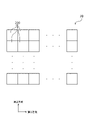
- FIG. 2 is a diagram showing a sparse array provided in the imaging device 2.
- FIG. The imaging device 2 has a pixel array 20 as a light receiving area.
- Pixel array 20 comprises a plurality of pixels 200 .
- the pixels 200 are arranged in an array along the first direction and the second direction, for example.
- the directions are given as an example, and are not limited to the first direction and the second direction. As another non-limiting example, the directions may be 45 degrees offset from the first and second directions, or any other angular offset.
- the pixels 200 are light-receiving pixels, and each pixel 200 may be configured to receive light of a predetermined color.
- the color of the light obtained by the pixel 200 may be, as a non-limiting example, the three primary colors of R (red), G (green), and B (blue).
- at least one of the three colors Cy (cyan), Mg (magenta), and Ye (yellow) may be further provided, and the light intensity of W (white) may be received.
- Colors received by the light-receiving element may be determined by, for example, providing a color filter on the incident surface of the light-receiving element, or providing the light-receiving element with an organic photoelectric conversion film. Also, an infrared cut filter may be used as the filter.
- the analog signal for each color photoelectrically converted by the light receiving element is appropriately converted into a digital signal by an A/D (Analog to Digital) conversion circuit provided inside or outside the imaging element 2.
- a path to the A/D conversion circuit and a circuit forming the A/D conversion circuit may be a circuit equivalent to a general CMOS (Complementary Metal Oxide Semiconductor) sensor, so the details are omitted.
- CMOS Complementary Metal Oxide Semiconductor
- an A/D conversion circuit is provided for each pixel or for each column, and analog signals output from the pixels 200 are appropriately converted into digital signals and output.
- the output digital signal is output to an appropriate circuit through a route equivalent to that of a general circuit.
- FIG. 3 is a diagram showing some pixels 200 extracted from the pixel array 20 according to one embodiment.
- the pixel 200 may be configured to receive light of the same color every four pixels, for example.
- the pixels 200 may be arranged in a Bayer array with these four pixels as a unit.
- they may be arranged in a checkerboard pattern, but the arrangement of colors is not limited to these examples as long as they are appropriately arranged in a mosaic pattern.
- pixels that receive R, pixels that receive G, and pixels that receive B are arranged as illustrated.
- the shaded pixels are light-shielding pixels 202 having a light-shielding structure inside the pixels.
- the light-shielding pixel 202 shields part of the light incident from the incident surface side, receives the light, and converts the intensity of the light in the light-shielded state into an analog signal.
- Other pixels 200 are pixels that photoelectrically convert light received through a color filter or the like, as usual.
- the light-shielded pixels 202 are arranged, for example, so as not to be adjacent to the pixels (8-connected pixels) that are oblique to the top, bottom, left, and right. Also, the light-shielded pixels 202 may be arranged periodically in the pixel array 20 .
- the light-shielding pixel 202 is not included in the group of pixels that receive G light, but it is not limited to this.
- at least one pixel in the pixel group that receives G light may be the light-shielded pixel 202 .
- FIG. 4 is a diagram schematically showing an example of the light-shielded pixel 202.
- the light-shielding pixel 202 includes, for example, a light-shielding film or an absorbing film as a light-shielding structure within the pixel.
- the light-shielding pixel 202 includes a light-shielding film 204 and an aperture 206.
- FIG. 4 is a diagram schematically showing an example of the light-shielded pixel 202.
- the light-shielding pixel 202 includes, for example, a light-shielding film or an absorbing film as a light-shielding structure within the pixel.
- the light-shielding pixel 202 includes a light-shielding film 204 and an aperture 206.
- the light-shielding film 204 (or absorption film) is formed of a film that shields the entire visible light region or light in the wavelength region of the color received by the light-shielding pixel 202 .
- the light-shielding film 204 may be formed of, as non-limiting examples, an appropriate metal, or an organic material such as a color filter having a property of absorbing an appropriate wavelength range.
- the light shielding film 204 is a thin or thick film made of a material equivalent to the light shielding structure used for the dummy pixel. may
- the light-shielding film 204 has openings 206 to limit the area of light incident on the light-receiving elements of the light-shielding pixels 202 .
- the light-shielding pixel 202 photoelectrically converts the light incident through the aperture 206 and outputs an analog signal based on the intensity of the light incident through the aperture 206 .
- the size of the opening 206 formed by the light shielding film 204 may be 25% or less of the area of the light receiving region of the light receiving element.
- the size of the aperture 206 is 25 % size.
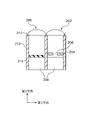
- FIG. 5 is an A-A cross-sectional view of the light-shielding pixel 202 shown in FIG. 4 as seen from the second direction. Adjacent pixels 200 are also shown.
- the pixels 200 and the light-shielding pixels 202 each have a light receiving area 208.
- the light-receiving element performs photoelectric conversion according to the intensity of the light incident on the incident surface side of the light-receiving region 208, and outputs an analog signal according to the received intensity.
- the light receiving region 208 is formed of, for example, a photodiode, an organic photoelectric conversion film, or the like.
- the pixels 200 and the light shielding pixels 202 are shielded by the light shielding walls 210.
- the light shielding wall 210 may be, for example, a metal film.
- the light shielding wall 210 is a wall surface for preventing the light incident on the pixel 200 and the light shielding pixel 202 from leaking to the other pixels 200 and the light shielding pixel 202 .
- the surface of the light shielding wall 210 on the pixel 200 side is desirably a reflective surface in order to appropriately acquire the intensity of light incident on the pixel 200 .
- the surface of the light shielding wall 210 on the side of the light shielding pixel 202 is desirably a non-reflecting surface so as not to widen the angle of the light incident on the light shielding pixel 202 .
- the light shielding wall 210 is not limited to this, and since the incidence of the light reflected by the light shielding wall 210 into the opening 206 can be controlled by the optical system, the light shielding wall 210 may also be a reflecting surface on the light shielding pixel 202 side.
- An on-chip lens 212 is provided for each of the pixels 200 and the light-shielding pixels 202 . Via the on-chip lens 212, the pixel 200 and the light-shielding pixel 202 allow light to enter the light receiving area.
- the light shielding film 204 partially prevents light incident through the on-chip lens 212 from entering the light receiving area 208 in the light shielding pixel 202 .
- the solid arrows for pixels 200 and the dotted arrows for light-shielded pixels 202 indicate light incidence from certain angles. Actually, the light is refracted twice at the interface of the on-chip lens 212, but the arrows indicate the directions before and after the on-chip lens 212 to simplify the explanation.
- the light-shielding film 204 as a light-shielding structure in this way, it is possible to limit the incident angle of light incident on the light-receiving region 208 through the opening 206 .
- the incident angle of light incident on the light receiving region of the light-shielding pixel 202 is adjusted to the light receiving region of the pixel 200 in order to sufficiently weaken the intensity of the flare. It can also be 50% or less of the incident angle of the light.
- any suitable incident angle may be obtained based on the arrangement and shape of the opening 206 in the on-chip lens and the light shielding film 204 .
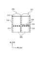
- FIG. 6 is cross-sectional views showing another non-limiting example of the pixel 200 and the shaded pixel 202.
- FIG. As described above, the pixels 200 and the light-shielding pixels 202 receive light in appropriate color wavelength regions using color filters or the like. These figures are examples in which the pixels 200 and the light-shielded pixels 202 are provided with color filters.
- a color filter 214 is provided above the light shielding film 204.
- FIG. 6 the light may already be converted into light limited to a desired wavelength region at the timing of incidence on the opening 206 of the light shielding film 204 .
- the color filter 214 need not be adjacent to the light shielding film 204 as shown in FIG.
- An interlayer insulating film or the like may be provided.
- FIG. 7 is another example in which a color filter 214 is provided above the light shielding film 204.
- a color filter 214 may be provided adjacent to the on-chip lens 212 .
- FIG. 8 shows an example in which a color filter 214 is provided under the light shielding film 204.
- FIG. 8 shows an example in which a color filter 214 is provided under the light shielding film 204.
- FIG. 8 shows an example in which a color filter 214 is provided under the light shielding film 204.
- light passing through openings 206 of light shielding film 204 may enter light receiving region 208 via color filter 214 .
- an interlayer insulating film or the like may be provided between the light shielding film 204 and the color filter 214, as in the case of providing it above the light shielding film 204. Further, an interlayer insulating film or the like may be provided between the color filter 214 and the light receiving region 208.
- FIG. 1 A block diagram illustrating an exemplary computing environment in accordance with the present disclosure.
- FIG. 9 is a diagram showing another example of arrangement of the color filters 214 in the pixels 200 and the light-shielding pixels 202.
- the pixels 200 are provided with color filters 214 so that the light-receiving regions 208 receive light of appropriate colors, while the light-shielding pixels 202 are provided with color filters 214 to receive white light. may not be provided.
- FIG. 10 is a diagram showing another example of the arrangement of filters in the pixel 200 and the light-shielded pixel 202.
- the pixel 200 may comprise a color filter 214 and the shaded pixel 202 may comprise an ND filter 216 (Neutral Density filter).
- ND filter 216 Neutral Density filter
- the light incident angle and the light incident area (incidence intensity) in the light receiving region are smaller (lower) than those of the normal pixel 200, as described above. Therefore, in the light-shielded pixel 202, the light from the light source can be acquired as low-luminance information without performing shutter control, exposure control, or the like. That is, even when there is a light source with high intensity on the display side, by acquiring information from the light-shielding pixels 202, the imaging element 2 can acquire a signal for detecting the shape of this light source. .
- the filter is located below the light shielding film 204 , but it is not limited to this. Also in such a filter configuration, the filter may be above the light shielding film 204 as shown in FIGS.
- FIG. 11 is a diagram showing an example of an image acquired by the imaging device 2 when there is a light source with high intensity on the imaging plane side.
- the hatched area is an area where an image can be properly acquired
- the white area is an area where an image cannot be properly acquired due to flare.
- flare may occur around the position of the light source, as shown in this figure.
- the flare is emphasized for easy understanding, but in reality, the more the position of the light source deviates from the center position, the smaller the influence of the flare may be.
- the influence of flare is reduced by signal processing and image processing.
- the shape of the light source detected by the light-shielded pixels 202 is used to perform correction processing using the PSF.
- FIG. 12 is a diagram showing an example of the shape of the light source detected from the image acquired from the light-shielding pixel 202 when the image of FIG.
- the shape of the light source as shown in FIG. 12 can be detected based on the signal acquired by the light shielding pixel 202.
- the shape of the light source may be detected by binarizing the image signal obtained based on the signal from the light-shielded pixel 202 using a static or dynamic threshold value.
- Fig. 13 is an acquired image of the effect of flare estimated based on the PSF according to the shape of the light source and the light intensity of the light source in Fig. 12.
- the influence of this flare may be obtained, for example, based on the PSF obtained by capturing strong light in advance.
- the influence of flare may be estimated by acquiring information about the PSF and convoluting this PSF information with the light source.
- a neural network model is learned by machine learning using this shape and intensity information and the acquired flare image as training data.
- Machine learning may include any technique, eg, any technique related to deep learning.
- the influence of flare may be inferred based on the shape and intensity information of the light source detected based on the signal output from the light-shielded pixel 202 to this neural network model.
- This neural network model may be a model in which at least one layer is formed by convolutional layers.
- FIG. 14 is a diagram showing an example of an image from which the influence of flare has been removed. For example, by subtracting the image in FIG. 13 from the image in FIG. 11, an image in which the influence of flare is properly removed can be obtained as shown in FIG.
- the shape of the light source can be acquired as white light, and the influence of flare caused by the white light can be removed.
- the color filters 214 may be arranged, for example, so that the color filters 214 provided in the light-shielding pixels 202 form a Bayer array, without being bound by the color of the pixel group to which the light-shielding pixels 202 belong.
- the pixel group of G in FIG. 3 may also be provided with the light-shielding pixel 202, and may be provided with the color filter 214 of the same color as the pixel group to which the light-shielding pixel 202 belongs.
- FIG. 15 is a block diagram schematically showing the imaging element 2 according to one embodiment.
- the imaging device 2 includes the pixel array 20, the storage section 22, the signal processing section 24, and the output section 26 described above. Also, the display 4 is provided with an optical module 40 , but a part of this may be mounted as the imaging device 2 .
- the optical module 40 is a module that includes, for example, an aperture arranged in the material of the display 4 and a module lens, and allows light from the display surface side of the display 4 to enter the pixel array 20 appropriately. Also, the optical module 40 may appropriately include an infrared cut filter or the like.
- a polarizing plate or the like may be provided in the opening.
- the module lens is a lens arranged so that the light transmitted through the aperture is appropriately incident on the pixel array 20, and is provided separately from the on-chip lens 212 described above.
- the pixel array 20 includes, for example, the pixels 200 having the structures shown in FIGS. 3 to 10 and the light-shielding pixels 202 arranged in the array shown in FIG.
- the storage unit 22 is composed of a memory, a storage, etc., which appropriately stores any information that should be stored in the imaging device 2 .
- the signal processing unit 24 is formed by, for example, a signal processing circuit, and appropriately processes and outputs analog signals output from the pixels 200 and the light-shielded pixels 202 .
- the output unit 26 appropriately outputs the signal processed by the signal processing unit 24 to the outside, or stores it in a storage unit provided inside the imaging element.
- the imaging device 2 appropriately includes components necessary for operation, such as a control unit for controlling each configuration of the imaging device 2.
- the signal processing unit 24 includes, for example, an A/D conversion circuit that converts analog signals output from the pixel array 20 into digital signals, and a logic circuit that converts the digital signals into signals suitable for output.
- the analog signals photoelectrically converted in the pixels 200 and the light-shielded pixels 202 of the pixel array 20 are converted into digital signals (digital image signals) by the A/D conversion circuit of the signal processing section 24 and output. If there is no need for signal processing or image processing after this, this digital image signal is output via the output section 26 .
- the image signals output from the light-shielded pixels 202 converted by the A/D conversion circuit are used to detect the shape of the light source.
- the signal processing unit 24 reconstructs a high-brightness image from the thinned image signals obtained from the light-shielded pixels 202 . From this reconstructed image, the shape of the light source is detected using, for example, an arbitrary threshold as described above. In addition to this shape detection, the signal processing section 24 may also detect the light intensity of the light source.
- the signal processing unit 24 that acquires the shape of the light source may perform processing for interpolating pixels at the positions of the light-shielded pixels 202 in the image based on the image signals output from the pixels 200 and the light-shielded pixels 202 .
- This interpolation can use a general defect correction method.
- the signal processing unit 24 calculates the influence of flare or the like based on the shape of the light source obtained from the light-shielded pixels 202. By calculating this effect, the signal processing unit 24 acquires image information indicating the effect of flare or the like as shown in FIG.
- the signal processing unit 24 appropriately subtracts the image information indicating the influence of flare or the like from the image information in which the influence of flare or the like has not been removed, thereby removing the influence of flare or the like shown in FIG. Image information can be acquired.
- the signal processing unit 24 performs other necessary processing to acquire an appropriate image signal. For example, demosaic processing, linear matrix processing, or other processing that makes the data suitable for display may be performed, or processing such as various filter processing may be performed.
- the signal processing unit 24 executes all the processing. detection circuit), a light-shielded pixel correction section (light-shielded pixel correction circuit), and a flare correction section (flare correction circuit). These circuits may be formed of analog or digital circuits as appropriate.
- the digital circuit may be any circuit such as ASIC (Application Specific Integrated Circuit), FPGA (Field-Programmable Gate Array), or the like.
- the present embodiment it is possible to accurately remove the effects of flare and the like on the captured image by providing the light-shielding pixels having the light-shielding structure in the light-receiving pixels. Since the imaging device according to the present embodiment does not require exposure control, double exposure, or the like, it is possible to acquire more appropriate images efficiently.
- FIG. 16 is a diagram showing an arrangement example of apertures 206 in light-shielded pixels 202. As shown in FIG. For example, as shown in FIG. 16, each light-shielding pixel 202 may have openings 206 that have the same shape and size, but different positions within the pixel.
- the imaging device 2 can separate the reflected light from the subject and the diffracted light generated in the display 4. It becomes possible.
- FIG. 17 is a diagram showing an arrangement example of apertures 206 in light-shielded pixels 202. As shown in FIG. For example, as shown in FIG. 17, each light-shielding pixel 202 may have apertures 206 that are located at the same position within the pixel and have different sizes.
- the diffracted light in the display 4 influences the received brightness value as the incident angle becomes smaller.
- the incident angle is disturbed by diffraction or the like that occurs in close proximity, whether or not light enters the aperture 206 with a small incident angle varies greatly. Therefore, by providing the apertures 206 with different incident angles, it is possible to analyze the image for each size of the apertures 206 to determine whether the light received by the light-shielding pixels 202 is reflected from the subject or not on the display 4. It is possible to make it easier to determine whether it is diffraction.
- FIG. 18 is a diagram showing still another arrangement example of the apertures 206 in the light-shielded pixels 202. As shown in FIG. As shown in FIG. 18, apertures 206 with different sizes and positions within the pixel may be provided. Also, although the shape is circular, it is not limited to this, and may be any other shape such as a rectangle, an ellipse, or the like.
- the accuracy of flare detection is further improved by appropriately changing the size of the aperture 206 and the relative position within the pixel. It is possible to
- the electronic device 1 is provided with one imaging element 2, but is not limited to this.
- the electronic device 1 may include two or more imaging elements 2.
- FIG. 19 shows an external view of the electronic device 1 according to one embodiment.
- the electronic device 1 includes two imaging elements 2a and 2b. In this way, the imaging element can also be configured with a compound eye.
- the electronic device 1 may include two imaging elements 2a and 2b with different imaging characteristics. Also, the characteristics of the two imaging elements 2a and 2b may be the same.
- the image sensor 2a includes the light-shielded pixels 202 as described above, and the image sensor 2b has the same pixel array configuration as the image sensor 2a. It is good also as a pixel which carries out.
- the configuration of the optical module 40 in FIG. 15 may be changed.
- one may be provided with an infrared cut filter and the other may be configured without an infrared cut filter.
- the imaging elements 2a and 2b may be configured to have polarization filters with different polarization directions.
- the imaging devices 2a and 2b may be configured to include module lenses with different characteristics.
- the accuracy of light source detection in the light-shielded pixels 202 can be improved by using parallax. For example, since diffraction on the display 4 causes a large parallax, it is possible for the signal processing unit 24 to perform correction to reduce the influence of diffraction on the display 4 based on the intensity of light received by the light-shielded pixels 202 .
- the imaging device 2a has a pixel array 20 that includes arrayed pixels 200 and light-shielded pixels 202 along the first direction and the second direction
- the imaging device 2b has the pixel array 20 arranged in the first direction and the second direction.
- a configuration in which the pixels 200 and the light-shielded pixels 202 are arrayed in a direction rotated by 45 degrees with respect to the second direction may be employed.
- the image sensor 2a can acquire information in the direction of the array
- the image sensor 2b can acquire information in a direction rotated 45 degrees from the direction of the array. becomes. Therefore, it is possible to improve the accuracy of detecting the shape of the light source and correcting the defect in the light-shielded pixel 202 .
- the electronic device can also include a plurality of imaging elements. These imaging devices can correct and interpolate mutually output images.
- the light-shielding pixels 202 were formed in the light-shielding film 204, but control of the amount of light in the light-shielding pixels 202 is not limited to this.
- FIG. 20 is a diagram schematically showing the pixel array 20 according to one embodiment.
- the light-shielding pixels 202 hatched in the drawing are each provided with a polarizing element that polarizes light in the direction of the hatched lines.
- the polarizing element may be, for example, a polarizing filter.
- the amount of light can be changed.
- a polarizing element is provided, the influence of flare can be removed with higher accuracy based on the signal obtained by the light-shielding pixel 202 by obtaining the polarization state of the reflected light on the display 4 in advance.
- the light-shielding pixel 202 may be configured to receive light in any other wavelength region such as W.
- the unit of the light-receiving and partially light-shielding region is the pixel unit, but the present invention is not limited to this.
- the pixel 200 divided pixels that share an on-chip lens, a light receiving element, and a pixel circuit may be formed, and a region partially shielded from light may be provided in units of the divided pixels.
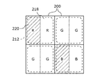
- FIG. 21 is a diagram showing an example of a pixel 200 and divided pixels according to one embodiment. Boundaries indicated by solid lines indicate boundaries of pixels, and boundaries indicated by dotted lines indicate churches of divided pixels. As shown in FIG. 21, the pixel 200 includes a plurality of divided pixels 218 and divided light-shielded pixels 220. As shown in FIG. The divided pixel 218 and the divided light-shielded pixel 220 belonging to the same pixel 200 may share the on-chip lens, light receiving element, and pixel circuit as described above.
- FIG. 22 is a cross-sectional view of the portion related to the R pixel extracted from the B-B cross section in FIG. Pixel 200 includes divided pixels 218 and divided shaded pixels 220 .
- the divided pixel 218 is provided with a color filter 214, and the divided light-shielding pixel 220 is further provided with a light-shielding film 204.
- the light receiving regions 208 of the plurality of divided pixels 218 are provided with element isolation films 222 as shown.
- the element isolation film 222 is a layer that isolates the light receiving regions of the divided pixels 218, and is made of metal or insulator, for example.
- a memory area forming a memory area may be provided for each light receiving area 208 .
- the divided light-shielded pixels 220 may be formed by providing the light-shielding films 204 in some of the divided pixels 218 .
- a polarizing element may be provided instead of the light shielding film 204 as described above.
- FIG. 23 is a diagram showing another example of shielding divided pixels.
- the number of divided pixels provided in the pixel 200 is not limited to 2 ⁇ 2, and there may be more divided pixels than 2 ⁇ 1 or 2 ⁇ 2.
- an on-chip lens 212 may be placed for each pixel 200.
- FIG. 24 is a diagram showing another example of shielding divided pixels.
- the pixels 200 and the light-shielded pixels 202 may each constitute divided pixels.
- the divided light-shielded pixels 220 of the light-shielded pixel 202 may each have an aperture 206 .
- a light-shielded region may be provided in the divided pixel as in the present embodiment. It should be noted that, as in the above-described embodiment, the arrangement of colors and the like are given as some non-limiting examples, and the aspects of the present disclosure are not limited to these examples.
- the divided light-shielding pixels 220 may be formed by a polarizing element instead of the light-shielding film 204. FIG.
- the imaging device 2 can detect diffracted light in the display 4.
- the structure is not limited to detection of diffracted light.
- the imaging device 2 As an imaging device for fingerprint authentication, it becomes possible to use the imaging device 2 as an imaging device for fingerprint authentication.
- the image sensor 2 acquires the reflected light of the light emitted from the display 4 on the finger in contact with the cover glass 5, the fingerprint is reproduced using the image signal output from the light-shielded pixel 202 or the divided light-shielded pixel 220. may be configured. Reflected light is diffusely reflected at the locations where the ridges of the fingerprint and the cover glass 5 are in contact, while the angle of incidence and the angle of reflection on the surface of the cover glass 5 coincide with each other in the regions of valleys of the fingerprint. Therefore, by acquiring the intensity of the light received by the light-shielding pixels 202 whose incident angles are limited, it is possible to reconstruct an appropriate fingerprint image.
- the position of the barcode can be set within 10 cm from the display 4 or the like.
- Information about such a subject at a relatively short distance from the display 4 may be reconstructed from information received by the light-shielded pixels 202 .
- the distance is within 10 cm, but depending on the situation, it may be set to any distance such as within 5 cm.
- the electronic device 1 may control macro photography mode, fingerprint authentication mode, barcode reading mode, and the like. This mode may be switched by the user.
- the light source, reading pixels, etc. may be appropriately controlled so as to obtain a fingerprint image based on the output from the light-shielded pixels 202. That is, the signal processing unit 24 may control the pixel values from the signals output from the pixels 200 and the light-shielded pixels 202 so that the fingerprint information can be easily obtained. For example, an image may be constructed by multiplying the signal output from the light-shielded pixel 202 by a gain of 1 or more, and controlling the effect of the signal output from the light-shielded pixel 202 to increase. After reconstructing the fingerprint image, the signal processing unit 24 may perform fingerprint authentication using a general technique.
- the signal processing unit 24 may control image reconstruction so as to increase the influence of the output from the light-shielded pixel 202 .
- the light shielding structure is explained using the light shielding film, the absorbing film, and the polarizing element, but the light shielding structure is not limited to this.
- this embodiment a case will be described in which light-shielded pixels and pixels to which a plasmon filter is applied as pixels other than the light-shielded pixels are used.
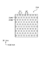
- FIG. 25 is a diagram showing an example of a plasmon filter.
- the plasmon filter 224 is formed by arranging holes 224b in a honeycomb pattern in a metal (or any conductor) thin film 224a. With this structure, the plasmon filter 224 generates a plasmon resonance phenomenon based on the aperture size D1 and the pitch a0 of the holes 224b.
- Each hole 224b penetrates the thin film 224a and acts as a waveguide.
- Waveguides generally have a cutoff frequency and a cutoff wavelength defined by a size such as a diameter, and have the property of not propagating light of a frequency lower than that (or a wavelength higher than that).
- the cutoff wavelength of hole 224b depends on the aperture size D1 and pitch a0 of hole 224b. The larger the aperture size D1, the longer the cut-off wavelength, and the smaller D1, the shorter the cut-off wavelength.
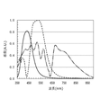
- FIG. 26 is a graph showing transmission wavelengths when the plasmon filter 224 is used.
- a solid line indicates a pitch of 250 nm
- a dashed line indicates a pitch of 325 nm
- a dashed line indicates a pitch of 500 nm.
- the plasmon filter 224 blocks light at the cut-off wavelength and operates in waveguide mode at wavelengths below the cut-off wavelength and in plasmon mode at wavelengths above the cut-off wavelength.
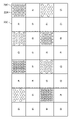
- FIG. 27 is an arrangement example of the plasmon filter 224.
- FIG. As shown in this figure, plasmon filters 224 with different characteristics may be placed in the pixel 200 as in the previous embodiments.
- plasmon filters 224 By providing plasmon filters 224 with different characteristics, it is possible to estimate the light source. For example, light other than the cut-off wavelength in each plasmon filter 224 is received. A light source can be estimated based on this received light.
- the light source can be estimated by calculating the ratio of the signals output from the pixels 200 where the respective plasmon filters 224 are arranged. For example, the color temperature may be estimated based on the outputs of multiple plasmon filters 224 with different characteristics. This estimation is performed by the signal processing unit 24 . Then, the signal processing unit 24 may further calculate the gain for each color filter based on this estimated result, and use the value multiplied by this gain as the value of each color in each pixel.
- FIG. 28 is a diagram showing an example of a pixel in which the plasmon filter 224 and the light-shielding pixel 202 are arranged together. As shown in this figure, a configuration in which a plasmon filter 224 is provided in a pixel different from the light shielded pixel 202 may be employed.
- the use of the plasmon filter 224 also allows the estimation of the light source to be performed as described above. Therefore, when removing flare from the state of the light source, it is possible to more specifically analyze the color components of the flare.
- spoofing can be indicated by referring to the output from the pixel 200 in which the plasmon filter 224 is arranged.
- the reflection of light on living human skin changes significantly around a wavelength of 590 nm.
- the imaging device 2 that acquires multispectral information can be configured. Therefore, it is possible to acquire reflection characteristics at wavelengths around 590 nm in the information acquired as multispectrum.
- the signal processing unit 24 can determine whether or not the subject in contact with the cover glass 5 is a living body. Therefore, the electronic device 1 equipped with the imaging element 2 can perform fingerprint authentication and determine whether or not the fingerprint information is reflected from the living body.
- the plasmon filter 224 may be arranged with respect to the divided pixel 218 when the pixel 200 includes divided pixels.
- the imaging device 2 may be configured to acquire vein information and hemoglobin information instead of fingerprint information. Also, instead of these pieces of information, the imaging device 2 may acquire information on oxygen saturation in blood.
- the image sensor 2 may acquire information on the iris of the human eye.
- the display 4 may be configured to emit light to the extent that it does not damage human eyes.
- the authentication operation using the imaging element 2 may be realized by acquiring one or more pieces of biometric information in the electronic device 1 .
- the electronic device 1 may include a plurality of imaging elements having split pixels as in the fifth embodiment, as in the third embodiment. In such a case, it is possible to interpolate in a form in which the other output of the light-shielded pixel 202 or the divided light-shielded pixel 220 is not light-shielded.
- Other embodiments can be appropriately combined in the same manner.
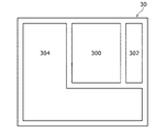
- FIG. 29 is a diagram showing an example of a substrate provided with the imaging element 2.
- FIG. Substrate 30 includes pixel area 300 , control circuitry 302 , and logic circuitry 304 . As shown in FIG. 29, the pixel region 300, the control circuit 302, and the logic circuit 304 may be arranged on the same substrate 30. FIG.
- a pixel region 300 is, for example, a region in which the pixel array 20 and the like described above are provided.
- the pixel circuits and the like described above may be appropriately provided in this pixel region 300 or may be provided in another region (not shown) of the substrate 30 .
- the control circuit 302 has a control section.
- the logic circuit 304 for example, the A/D conversion circuit of the signal processing unit 24 may be provided in the pixel region 300 and the converted digital signal may be output to the logic circuit 304.
- the image processing section (for example, part of the circuit of the signal processing section 24) may be provided in this logic circuit 304.
- FIG. At least part of the signal processing unit 24 and the image processing unit may be mounted not on this chip but on another signal processing chip provided at a location different from the substrate 30, or may be mounted in another processor. may be implemented in
- FIG. 30 is a diagram showing another example of a substrate provided with an imaging device 2.
- a first substrate 32 and a second substrate 34 are provided.
- the first substrate 32 and the second substrate 34 have a laminated structure, and can transmit and receive signals to and from each other appropriately through connection portions such as via holes.
- the first substrate 32 may comprise the pixel area 300 and the control circuit 302, and the second substrate 34 may comprise the logic circuit 304.
- FIG. 31 is a diagram showing another example of a substrate provided with an imaging device 2.
- a first substrate 32 and a second substrate 34 are provided.
- the first substrate 32 and the second substrate 34 have a laminated structure, and signals can be transmitted and received to and from each other appropriately through connection portions such as via holes.
- the first substrate 32 may comprise the pixel area 300 and the second substrate 34 may comprise the control circuit 302 and the logic circuit 304 .
- the storage area may be provided in an arbitrary area.
- a substrate for storage area may be provided, and this substrate may be provided between the first substrate 32 and the second substrate 34 or below the second substrate 34. .
- a plurality of stacked substrates may be connected to each other through via holes as described above, or may be connected by a method such as micro-dumping. These substrates can be laminated by any method such as CoC (Chip on Chip), CoW (Chip on Wafer), or WoW (Wafer on Wafer).
- FIG. 32A and 32B are diagrams showing the internal configuration of a vehicle 360, which is a first application example of the electronic device 1 including the imaging device 2 according to the present disclosure.
- 32A is a view showing the interior of the vehicle 360 from the rear to the front of the vehicle 360
- FIG. 32B is a view showing the interior of the vehicle 360 from the oblique rear to the oblique front of the vehicle 360.
- a vehicle 360 in FIGS. 32A and 32B has a center display 361, a console display 362, a heads-up display 363, a digital rear mirror 364, a steering wheel display 365, and a rear entertainment display 366.
- the center display 361 is arranged on the dashboard 367 at a location facing the driver's seat 368 and the passenger's seat 369.
- FIG. 32 shows an example of a horizontally elongated center display 361 extending from the driver's seat 368 side to the passenger's seat 369 side, but the screen size and location of the center display 361 are arbitrary.
- Information detected by various sensors can be displayed on the center display 361 .
- the center display 361 displays images captured by the image sensor, images of the distance to obstacles in front of and to the side of the vehicle measured by the ToF sensor, and passenger temperatures detected by the infrared sensor. Displayable.
- Center display 361 can be used to display at least one of safety-related information, operation-related information, lifelogs, health-related information, authentication/identification-related information, and entertainment-related information, for example.
- Safety-related information includes information such as the detection of falling asleep, the detection of looking away, the detection of tampering by children riding in the same vehicle, the presence or absence of seatbelt wearing, and the detection of occupants being left behind. It is information detected by The operation-related information uses a sensor to detect a gesture related to the operation of the passenger. Detected gestures may include manipulating various equipment within vehicle 360 . For example, it detects the operation of an air conditioner, a navigation device, an AV device, a lighting device, or the like.
- the lifelog includes lifelogs of all crew members. For example, the lifelog includes a record of each occupant's behavior during the ride.
- the health-related information detects the body temperature of the occupant using a temperature sensor, and infers the health condition of the occupant based on the detected body temperature.
- an image sensor may be used to capture an image of the occupant's face, and the occupant's health condition may be estimated from the captured facial expression.
- an automated voice conversation may be conducted with the passenger, and the health condition of the passenger may be estimated based on the content of the passenger's answers.
- Authentication/identification-related information includes a keyless entry function that performs face authentication using a sensor, and a function that automatically adjusts seat height and position by face recognition.
- the entertainment-related information includes a function of detecting operation information of the AV device by the passenger using a sensor, a function of recognizing the face of the passenger with the sensor, and providing content suitable for the passenger with the AV device.
- the console display 362 can be used, for example, to display lifelog information.
- Console display 362 is located near shift lever 371 on center console 370 between driver's seat 368 and passenger's seat 369 .
- a console display 362 can also display information detected by various sensors.
- the console display 362 may display an image of the surroundings of the vehicle captured by an image sensor, or may display an image of the distance to obstacles around the vehicle.
- the head-up display 363 is virtually displayed behind the windshield 372 in front of the driver's seat 368. Heads-up display 363 can be used to display at least one of safety-related information, operation-related information, lifelogs, health-related information, authentication/identification-related information, and entertainment-related information, for example.
- the heads-up display 363 is often placed virtually in front of the driver's seat 368 and is therefore used to display information directly related to the operation of the vehicle 360, such as vehicle 360 speed and fuel (battery) level. Are suitable.
- the digital rear mirror 364 can display not only the rear of the vehicle 360 but also the state of the passengers in the rear seats. be able to.
- the steering wheel display 365 is arranged near the center of the steering wheel 373 of the vehicle 360.
- Steering wheel display 365 can be used, for example, to display at least one of safety-related information, operational-related information, lifelogs, health-related information, authentication/identification-related information, and entertainment-related information.
- life log information such as the driver's body temperature and information regarding the operation of AV equipment and air conditioning equipment.
- the rear entertainment display 366 is attached to the back side of the driver's seat 368 and passenger's seat 369, and is intended for viewing by passengers in the rear seats.
- Rear entertainment display 366 can be used to display at least one of safety-related information, operation-related information, lifelogs, health-related information, authentication/identification-related information, and entertainment-related information, for example.
- information relevant to the rear seat occupants is displayed. For example, information about the operation of an AV device or an air conditioner may be displayed, or the results obtained by measuring the body temperature of passengers in the rear seats with a temperature sensor may be displayed.
- Optical distance measurement methods are broadly classified into passive and active methods.
- the passive type measures distance by receiving light from an object without projecting light from the sensor to the object.
- Passive types include lens focusing, stereo, and monocular vision.
- the active type measures distance by projecting light onto an object and receiving reflected light from the object with a sensor.
- Active types include an optical radar method, an active stereo method, a photometric stereo method, a moire topography method, an interferometric method, and the like.
- the electronic device 1 according to the present disclosure is applicable to any of these methods of distance measurement.
- the passive or active distance measurement described above can be performed.
- the electronic device 1 including the imaging device 2 according to the present disclosure can be applied not only to various displays used in vehicles, but also to displays mounted on various electronic devices.
- FIG. 33A is a front view of a digital camera 310, which is a second application example of the electronic device 1, and FIG. 33B is a rear view of the digital camera 310.
- FIG. A digital camera 310 in FIGS. 33A and 33B shows an example of a single-lens reflex camera with an interchangeable lens 121, but it is also applicable to a camera in which the lens 121 is not interchangeable.
- FIGS. 33A and 33B In the camera of FIGS. 33A and 33B, when the photographer holds the grip 313 of the camera body 311, looks through the electronic viewfinder 315, determines the composition, adjusts the focus, and presses the shutter, the Captured data is stored in memory.
- a monitor screen 316 for displaying photographed data and the like, a live image and the like, and an electronic viewfinder 315 are provided on the rear side of the camera.
- a sub-screen for displaying setting information such as shutter speed and exposure value is provided on the upper surface of the camera.
- the senor By arranging the sensor on the back side of the monitor screen 316, the electronic viewfinder 315, the sub-screen, etc. used for the camera, it can be used as the electronic device 1 according to the present disclosure.
- the electronic device 1 according to the present disclosure can also be applied to a head-mounted display (hereinafter referred to as HMD).
- HMDs can be used for VR, AR, MR (Mixed Reality), SR (Substitutional Reality), and the like.
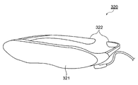
- FIG. 34A is an external view of the HMD 320, which is the third application example of the electronic device 1.
- FIG. The HMD 320 of Figure 34A has a mounting member 322 for mounting over the human eye. This mounting member 322 is fixed by being hooked on a human ear, for example.
- a display device 321 is provided inside the HMD 320 , and the wearer of the HMD 320 can visually recognize a stereoscopic image or the like on the display device 321 .
- the HMD 320 has, for example, a wireless communication function and an acceleration sensor, and can switch stereoscopic images and the like displayed on the display device 321 according to the posture and gestures of the wearer.
- the HMD 320 may be provided with a camera to capture an image of the wearer's surroundings, and the display device 321 may display an image obtained by synthesizing the image captured by the camera and an image generated by a computer.
- a camera is placed on the back side of the display device 321 that is visually recognized by the wearer of the HMD 320, and the area around the wearer's eyes is captured by this camera. By displaying it on the display, people around the wearer can grasp the wearer's facial expressions and eye movements in real time.
- FIG. 34B the electronic device 1 according to the present disclosure can also be applied to smart glasses 340 that display various information on glasses 344.
- FIG. A smart glass 340 in FIG. 34B has a body portion 341, an arm portion 342, and a barrel portion 343.
- Body portion 341 is connected to arm portion 342 .
- the body portion 341 is detachable from the glasses 344 .
- the main unit 341 incorporates a control board for controlling the operation of the smart glasses 340 and a display unit.
- the body portion 341 and the lens barrel are connected to each other via the arm portion 342 .
- the lens barrel portion 343 emits image light emitted from the body portion 341 via the arm portion 342 to the lens 345 side of the glasses 344 .
- This image light enters the human eye through lens 345 .
- the wearer of the smart glasses 340 in FIG. 34B can visually recognize not only the surroundings but also various information emitted from the lens barrel 343 in the same manner as ordinary glasses.
- the electronic device 1 according to the present disclosure can also be applied to a television device (hereinafter referred to as TV).
- TV television device
- Recent TVs tend to have a frame as small as possible from the viewpoint of miniaturization and design. For this reason, when a camera for photographing the viewer is provided on the TV, it is desirable to place the camera on the back side of the display panel 331 of the TV.
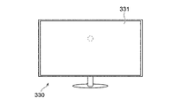
- FIG. 35 is an external view of a TV 330, which is a fourth application example of the electronic device 1.
- the frame of the TV 330 in FIG. 35 is minimized, and almost the entire front side is the display area.
- the TV 330 has a built-in sensor such as a camera for photographing the viewer.
- the sensor in FIG. 35 is arranged behind a portion of the display panel 331 (for example, the portion indicated by the dashed line).
- the sensor may be an image sensor module, and various sensors such as face authentication sensors, distance measurement sensors, and temperature sensors can be applied. may be placed.
- the image sensor module can be arranged overlapping the back side of the display panel 331, so there is no need to arrange a camera or the like in the frame, and the TV 330 can be miniaturized. In addition, there is no fear that the design will be spoiled by the frame.
- FIG. 36 is an external view of a smartphone 350, which is a fifth application example of the electronic device 1.
- the display surface 2z extends close to the external size of the electronic device 1, and the width of the bezel 2y around the display surface 2z is several millimeters or less.
- a front camera is often mounted on the bezel 2y, but in FIG. 36, an image sensor module 9 functioning as a front camera is mounted on the back side of the display surface 2z, for example, in the approximate center, as indicated by the dashed line. are placed.
- a pixel comprising a light-receiving element that photoelectrically converts incident light and outputs an analog signal based on the intensity of the light; a pixel array in which the pixels are arranged in an array; with Some of the pixels belonging to the pixel array have a light shielding structure that shields part of the light incident on the light receiving element. image sensor.
- the light shielding structure limits the angle of incidence of light incident on the light receiving element of the pixel provided with the light shielding structure.
- the light shielding structure is a light shielding film provided in the light receiving element, (2) The imaging device according to the above.
- the light shielding structure is formed so that the size of the opening in the pixel is 25% or less of the surface area of the light receiving element.
- the openings formed by the light shielding structure have the same size or different sizes depending on the pixels.
- the imaging device according to (3) is the same size or different sizes depending on the pixels.
- the apertures formed by the light shielding structures are provided by the pixels at the same or different relative positions in the pixels;
- the imaging device according to (3) or (5) The imaging device according to (3) or (5).
- one or more openings are formed by the light shielding structure;
- the imaging device according to any one of (3) to (6).
- the light shielding structure is a polarizer provided in the light receiving element, (2) The imaging device according to the above.
- the pixels having the light shielding structure are arranged in non-adjacent positions in the pixel array;
- the imaging device according to any one of (2) to (9).
- the pixels having the light shielding structure are arranged periodically in the pixel array; (10) The imaging device according to the above.
- An on-chip lens is provided for each pixel, A module lens is provided in the pixel array, The imaging device according to any one of (2) to (11).
- the pixel includes a divided pixel obtained by dividing the light receiving element belonging to the pixel into a plurality of pixels, the pixel having the light shielding structure has the light shielding structure for at least one of the divided pixels;
- the imaging device according to any one of (2) to (12).
- the signal processing circuit detects the shape of the light source based on the output from the pixel provided with the light shielding structure.
- the imaging device according to the above.
- the signal processing circuit estimates a light source based on the output from the pixel provided with the light shielding structure. (14) The imaging device according to the above.
- an imaging device according to any one of (14) to (17); a display having a display surface for displaying information on the incident surface side of the imaging device; with The imaging element converts light received through the display by photoelectric conversion. Electronics.
- the light shielding structure includes the pixel in which the incident angle at which light can enter is controlled to 50% or less of the normal angle, generating imaging information of a nearby object based on the output from the pixel having the light shielding structure;
- the biometric information is information including any one of fingerprints, iris, veins, skin, hemoglobin, or oxygen saturation, (20) Electronic equipment according to.
- the wiring layout of the display in at least one imaging element is different from the wiring layout of the display in the other imaging elements, The electronic device according to (24).
- 1 Electronics, 1a: display area, 1b: bezel, 2: image sensor, 3: component layer, 4: display, 5: coverslip, 20: pixel array, 200: pixels, 202: shading pixels, 204: light shielding film, 206: Aperture, 208: light receiving area, 210: Shading wall, 212: on-chip lens, 214: color filters, 216: ND filter, 218: division pixel, 220: divided shaded pixels, 222: element isolation film, 224: Plasmon Filter, 224a: thin film, 224b: hole, 22: storage unit, 24: signal processor, 26: output section,
Landscapes
- Engineering & Computer Science (AREA)
- Multimedia (AREA)
- Signal Processing (AREA)
- Solid State Image Pick-Up Elements (AREA)
Priority Applications (4)
| Application Number | Priority Date | Filing Date | Title |
|---|---|---|---|
| US18/556,752 US20240243145A1 (en) | 2021-05-17 | 2022-02-18 | Imaging element and electronic device |
| JP2023522234A JPWO2022244354A1 (https=) | 2021-05-17 | 2022-02-18 | |
| CN202280034645.XA CN117280471A (zh) | 2021-05-17 | 2022-02-18 | 成像元件和电子装置 |
| DE112022002630.8T DE112022002630T5 (de) | 2021-05-17 | 2022-02-18 | Bildgebungselement und elektronische vorrichtung |
Applications Claiming Priority (2)
| Application Number | Priority Date | Filing Date | Title |
|---|---|---|---|
| JP2021-083398 | 2021-05-17 | ||
| JP2021083398 | 2021-05-17 |
Publications (1)
| Publication Number | Publication Date |
|---|---|
| WO2022244354A1 true WO2022244354A1 (ja) | 2022-11-24 |
Family
ID=84140228
Family Applications (1)
| Application Number | Title | Priority Date | Filing Date |
|---|---|---|---|
| PCT/JP2022/006705 Ceased WO2022244354A1 (ja) | 2021-05-17 | 2022-02-18 | 撮像素子及び電子機器 |
Country Status (5)
| Country | Link |
|---|---|
| US (1) | US20240243145A1 (https=) |
| JP (1) | JPWO2022244354A1 (https=) |
| CN (1) | CN117280471A (https=) |
| DE (1) | DE112022002630T5 (https=) |
| WO (1) | WO2022244354A1 (https=) |
Families Citing this family (1)
| Publication number | Priority date | Publication date | Assignee | Title |
|---|---|---|---|---|
| JP2022105820A (ja) * | 2021-01-05 | 2022-07-15 | ソニーセミコンダクタソリューションズ株式会社 | 受光素子、撮像装置及び補正処理方法 |
Citations (6)
| Publication number | Priority date | Publication date | Assignee | Title |
|---|---|---|---|---|
| JP2011176715A (ja) * | 2010-02-25 | 2011-09-08 | Nikon Corp | 裏面照射型撮像素子および撮像装置 |
| JP2015026675A (ja) * | 2013-07-25 | 2015-02-05 | ソニー株式会社 | 固体撮像素子およびその製造方法、並びに電子機器 |
| WO2018061729A1 (ja) * | 2016-09-30 | 2018-04-05 | 株式会社ニコン | 撮像素子および焦点調節装置 |
| WO2019078336A1 (ja) * | 2017-10-19 | 2019-04-25 | ソニー株式会社 | 撮像装置および信号処理装置 |
| JP2019129178A (ja) * | 2018-01-22 | 2019-08-01 | ソニーセミコンダクタソリューションズ株式会社 | 半導体素子及び電子機器 |
| WO2019215192A1 (en) * | 2018-05-07 | 2019-11-14 | Wavetouch Limited | Compact optical sensor for fingerprint detection |
Family Cites Families (1)
| Publication number | Priority date | Publication date | Assignee | Title |
|---|---|---|---|---|
| JP5074564B2 (ja) | 2004-05-17 | 2012-11-14 | オリンパス株式会社 | 撮像装置、ノイズ除去方法およびノイズ除去プログラム |
-
2022
- 2022-02-18 WO PCT/JP2022/006705 patent/WO2022244354A1/ja not_active Ceased
- 2022-02-18 DE DE112022002630.8T patent/DE112022002630T5/de active Pending
- 2022-02-18 US US18/556,752 patent/US20240243145A1/en active Pending
- 2022-02-18 JP JP2023522234A patent/JPWO2022244354A1/ja not_active Abandoned
- 2022-02-18 CN CN202280034645.XA patent/CN117280471A/zh not_active Withdrawn
Patent Citations (6)
| Publication number | Priority date | Publication date | Assignee | Title |
|---|---|---|---|---|
| JP2011176715A (ja) * | 2010-02-25 | 2011-09-08 | Nikon Corp | 裏面照射型撮像素子および撮像装置 |
| JP2015026675A (ja) * | 2013-07-25 | 2015-02-05 | ソニー株式会社 | 固体撮像素子およびその製造方法、並びに電子機器 |
| WO2018061729A1 (ja) * | 2016-09-30 | 2018-04-05 | 株式会社ニコン | 撮像素子および焦点調節装置 |
| WO2019078336A1 (ja) * | 2017-10-19 | 2019-04-25 | ソニー株式会社 | 撮像装置および信号処理装置 |
| JP2019129178A (ja) * | 2018-01-22 | 2019-08-01 | ソニーセミコンダクタソリューションズ株式会社 | 半導体素子及び電子機器 |
| WO2019215192A1 (en) * | 2018-05-07 | 2019-11-14 | Wavetouch Limited | Compact optical sensor for fingerprint detection |
Also Published As
| Publication number | Publication date |
|---|---|
| DE112022002630T5 (de) | 2024-03-14 |
| US20240243145A1 (en) | 2024-07-18 |
| JPWO2022244354A1 (https=) | 2022-11-24 |
| CN117280471A (zh) | 2023-12-22 |
Similar Documents
| Publication | Publication Date | Title |
|---|---|---|
| JP7705383B2 (ja) | 電子機器及び撮像装置 | |
| KR102890119B1 (ko) | 촬상 소자 및 전자 기기 | |
| WO2017155622A1 (en) | Phase detection autofocus using opposing filter masks | |
| JP7667085B2 (ja) | 電子機器 | |
| CN112866518B (zh) | 电子设备 | |
| CN113286058B (zh) | 电子设备 | |
| US20240243145A1 (en) | Imaging element and electronic device | |
| US20240171868A1 (en) | Imaging element, imaging device and electronic device | |
| JP2013054121A (ja) | 撮像装置 |
Legal Events
| Date | Code | Title | Description |
|---|---|---|---|
| 121 | Ep: the epo has been informed by wipo that ep was designated in this application |
Ref document number: 22804275 Country of ref document: EP Kind code of ref document: A1 |
|
| WWE | Wipo information: entry into national phase |
Ref document number: 2023522234 Country of ref document: JP |
|
| WWE | Wipo information: entry into national phase |
Ref document number: 18556752 Country of ref document: US |
|
| WWE | Wipo information: entry into national phase |
Ref document number: 202280034645.X Country of ref document: CN |
|
| WWE | Wipo information: entry into national phase |
Ref document number: 112022002630 Country of ref document: DE |
|
| 122 | Ep: pct application non-entry in european phase |
Ref document number: 22804275 Country of ref document: EP Kind code of ref document: A1 |