WO2022244354A1 - Imaging element and electronic device - Google Patents
Imaging element and electronic device Download PDFInfo
- Publication number
- WO2022244354A1 WO2022244354A1 PCT/JP2022/006705 JP2022006705W WO2022244354A1 WO 2022244354 A1 WO2022244354 A1 WO 2022244354A1 JP 2022006705 W JP2022006705 W JP 2022006705W WO 2022244354 A1 WO2022244354 A1 WO 2022244354A1
- Authority
- WO
- WIPO (PCT)
- Prior art keywords
- light
- pixel
- pixels
- light shielding
- shielding structure
- Prior art date
Links
- 238000003384 imaging method Methods 0.000 title claims abstract description 130
- 238000006243 chemical reaction Methods 0.000 claims abstract description 14
- 238000012545 processing Methods 0.000 claims description 62
- 230000006866 deterioration Effects 0.000 claims description 4
- 238000010586 diagram Methods 0.000 description 50
- 239000010408 film Substances 0.000 description 50
- 239000000758 substrate Substances 0.000 description 29
- 238000000034 method Methods 0.000 description 16
- 239000010410 layer Substances 0.000 description 14
- 239000006059 cover glass Substances 0.000 description 13
- 238000012937 correction Methods 0.000 description 10
- 238000001514 detection method Methods 0.000 description 10
- 230000000694 effects Effects 0.000 description 10
- 208000013057 hereditary mucoepithelial dysplasia Diseases 0.000 description 10
- 230000006870 function Effects 0.000 description 8
- 230000036541 health Effects 0.000 description 8
- 230000003287 optical effect Effects 0.000 description 7
- 239000003086 colorant Substances 0.000 description 6
- 239000011521 glass Substances 0.000 description 5
- 239000004984 smart glass Substances 0.000 description 5
- 239000010409 thin film Substances 0.000 description 5
- 230000036760 body temperature Effects 0.000 description 4
- 239000002184 metal Substances 0.000 description 4
- 238000003062 neural network model Methods 0.000 description 4
- 102000001554 Hemoglobins Human genes 0.000 description 3
- 108010054147 Hemoglobins Proteins 0.000 description 3
- QVGXLLKOCUKJST-UHFFFAOYSA-N atomic oxygen Chemical compound [O] QVGXLLKOCUKJST-UHFFFAOYSA-N 0.000 description 3
- 239000011229 interlayer Substances 0.000 description 3
- 238000002955 isolation Methods 0.000 description 3
- 238000005259 measurement Methods 0.000 description 3
- 229910052760 oxygen Inorganic materials 0.000 description 3
- 239000001301 oxygen Substances 0.000 description 3
- 230000010287 polarization Effects 0.000 description 3
- 239000004065 semiconductor Substances 0.000 description 3
- 210000003462 vein Anatomy 0.000 description 3
- 230000005540 biological transmission Effects 0.000 description 2
- 230000007547 defect Effects 0.000 description 2
- 238000013461 design Methods 0.000 description 2
- 230000008921 facial expression Effects 0.000 description 2
- 238000010801 machine learning Methods 0.000 description 2
- 239000000463 material Substances 0.000 description 2
- 206010020772 Hypertension Diseases 0.000 description 1
- 238000010521 absorption reaction Methods 0.000 description 1
- 230000001133 acceleration Effects 0.000 description 1
- 238000007792 addition Methods 0.000 description 1
- 238000004378 air conditioning Methods 0.000 description 1
- 230000002547 anomalous effect Effects 0.000 description 1
- 230000006399 behavior Effects 0.000 description 1
- 239000008280 blood Substances 0.000 description 1
- 210000004369 blood Anatomy 0.000 description 1
- 230000008859 change Effects 0.000 description 1
- 238000004891 communication Methods 0.000 description 1
- 230000000295 complement effect Effects 0.000 description 1
- 150000001875 compounds Chemical class 0.000 description 1
- 239000004020 conductor Substances 0.000 description 1
- 238000013135 deep learning Methods 0.000 description 1
- 230000002950 deficient Effects 0.000 description 1
- 238000012217 deletion Methods 0.000 description 1
- 230000037430 deletion Effects 0.000 description 1
- 230000004424 eye movement Effects 0.000 description 1
- 239000000446 fuel Substances 0.000 description 1
- 238000007689 inspection Methods 0.000 description 1
- 239000012212 insulator Substances 0.000 description 1
- 230000007774 longterm Effects 0.000 description 1
- 239000011159 matrix material Substances 0.000 description 1
- 238000000691 measurement method Methods 0.000 description 1
- 229910044991 metal oxide Inorganic materials 0.000 description 1
- 150000004706 metal oxides Chemical class 0.000 description 1
- 239000000203 mixture Substances 0.000 description 1
- 238000012986 modification Methods 0.000 description 1
- 230000004048 modification Effects 0.000 description 1
- 230000007935 neutral effect Effects 0.000 description 1
- 239000011368 organic material Substances 0.000 description 1
- 230000008569 process Effects 0.000 description 1
- 230000001902 propagating effect Effects 0.000 description 1
- 230000011514 reflex Effects 0.000 description 1
- 239000007787 solid Substances 0.000 description 1
- 230000003068 static effect Effects 0.000 description 1
- 230000002194 synthesizing effect Effects 0.000 description 1
- 238000012876 topography Methods 0.000 description 1
- 238000012549 training Methods 0.000 description 1
Images


Classifications
-
- H—ELECTRICITY
- H01—ELECTRIC ELEMENTS
- H01L—SEMICONDUCTOR DEVICES NOT COVERED BY CLASS H10
- H01L27/00—Devices consisting of a plurality of semiconductor or other solid-state components formed in or on a common substrate
- H01L27/14—Devices consisting of a plurality of semiconductor or other solid-state components formed in or on a common substrate including semiconductor components sensitive to infrared radiation, light, electromagnetic radiation of shorter wavelength or corpuscular radiation and specially adapted either for the conversion of the energy of such radiation into electrical energy or for the control of electrical energy by such radiation
- H01L27/144—Devices controlled by radiation
- H01L27/146—Imager structures
- H01L27/14601—Structural or functional details thereof
- H01L27/1462—Coatings
- H01L27/14623—Optical shielding
-
- G—PHYSICS
- G03—PHOTOGRAPHY; CINEMATOGRAPHY; ANALOGOUS TECHNIQUES USING WAVES OTHER THAN OPTICAL WAVES; ELECTROGRAPHY; HOLOGRAPHY
- G03B—APPARATUS OR ARRANGEMENTS FOR TAKING PHOTOGRAPHS OR FOR PROJECTING OR VIEWING THEM; APPARATUS OR ARRANGEMENTS EMPLOYING ANALOGOUS TECHNIQUES USING WAVES OTHER THAN OPTICAL WAVES; ACCESSORIES THEREFOR
- G03B11/00—Filters or other obturators specially adapted for photographic purposes
-
- G—PHYSICS
- G03—PHOTOGRAPHY; CINEMATOGRAPHY; ANALOGOUS TECHNIQUES USING WAVES OTHER THAN OPTICAL WAVES; ELECTROGRAPHY; HOLOGRAPHY
- G03B—APPARATUS OR ARRANGEMENTS FOR TAKING PHOTOGRAPHS OR FOR PROJECTING OR VIEWING THEM; APPARATUS OR ARRANGEMENTS EMPLOYING ANALOGOUS TECHNIQUES USING WAVES OTHER THAN OPTICAL WAVES; ACCESSORIES THEREFOR
- G03B17/00—Details of cameras or camera bodies; Accessories therefor
- G03B17/18—Signals indicating condition of a camera member or suitability of light
-
- H—ELECTRICITY
- H01—ELECTRIC ELEMENTS
- H01L—SEMICONDUCTOR DEVICES NOT COVERED BY CLASS H10
- H01L27/00—Devices consisting of a plurality of semiconductor or other solid-state components formed in or on a common substrate
- H01L27/14—Devices consisting of a plurality of semiconductor or other solid-state components formed in or on a common substrate including semiconductor components sensitive to infrared radiation, light, electromagnetic radiation of shorter wavelength or corpuscular radiation and specially adapted either for the conversion of the energy of such radiation into electrical energy or for the control of electrical energy by such radiation
- H01L27/144—Devices controlled by radiation
- H01L27/146—Imager structures
- H01L27/14601—Structural or functional details thereof
- H01L27/14603—Special geometry or disposition of pixel-elements, address-lines or gate-electrodes
- H01L27/14605—Structural or functional details relating to the position of the pixel elements, e.g. smaller pixel elements in the center of the imager compared to pixel elements at the periphery
-
- H—ELECTRICITY
- H01—ELECTRIC ELEMENTS
- H01L—SEMICONDUCTOR DEVICES NOT COVERED BY CLASS H10
- H01L27/00—Devices consisting of a plurality of semiconductor or other solid-state components formed in or on a common substrate
- H01L27/14—Devices consisting of a plurality of semiconductor or other solid-state components formed in or on a common substrate including semiconductor components sensitive to infrared radiation, light, electromagnetic radiation of shorter wavelength or corpuscular radiation and specially adapted either for the conversion of the energy of such radiation into electrical energy or for the control of electrical energy by such radiation
- H01L27/144—Devices controlled by radiation
- H01L27/146—Imager structures
- H01L27/14601—Structural or functional details thereof
- H01L27/1462—Coatings
- H01L27/14621—Colour filter arrangements
-
- H—ELECTRICITY
- H01—ELECTRIC ELEMENTS
- H01L—SEMICONDUCTOR DEVICES NOT COVERED BY CLASS H10
- H01L27/00—Devices consisting of a plurality of semiconductor or other solid-state components formed in or on a common substrate
- H01L27/14—Devices consisting of a plurality of semiconductor or other solid-state components formed in or on a common substrate including semiconductor components sensitive to infrared radiation, light, electromagnetic radiation of shorter wavelength or corpuscular radiation and specially adapted either for the conversion of the energy of such radiation into electrical energy or for the control of electrical energy by such radiation
- H01L27/144—Devices controlled by radiation
- H01L27/146—Imager structures
- H01L27/14601—Structural or functional details thereof
- H01L27/14625—Optical elements or arrangements associated with the device
- H01L27/14627—Microlenses
Definitions
- the present disclosure relates to imaging devices and electronic devices.
- the present disclosure provides an imaging device that improves image quality.
- the imaging device includes pixels and a pixel array.
- a pixel includes a light receiving element that photoelectrically converts incident light and outputs an analog signal based on the intensity of the light.
- the pixels are arranged in an array in the pixel array. Some of the pixels belonging to the pixel array have a light shielding structure that shields part of the light incident on the light receiving element.
- the light shielding structure may limit the incident angle of light incident on the light receiving element of the pixel provided with the light shielding structure.
- the light shielding structure may be a light shielding film provided on the incident surface side of the light receiving element.
- the light shielding structure may be formed so that the size of the aperture in the pixel is 25% or less of the area of the surface of the light receiving element.
- the apertures formed by the light shielding structure may have the same size or different sizes depending on the pixels.
- the apertures formed by the light shielding structures may be provided at the same or different relative positions in the pixels depending on the pixels.
- one or more openings may be formed by the light shielding structure.
- the light shielding structure may be a polarizer provided on the incident surface side of the light receiving element.
- a pixel different from the pixel where the light shielding structure is arranged may include the pixel where the plasmon filter is arranged on the incident surface side of the light receiving element.
- the pixels having the light shielding structure may be arranged at non-adjacent positions in the pixel array.
- the pixels having the light shielding structure may be arranged periodically in the pixel array.
- An on-chip lens may be provided for each pixel, and a module lens may be provided for the pixel array.
- the pixel may include divided pixels obtained by dividing the light receiving element belonging to the pixel into a plurality of pixels, and the pixel having the light shielding structure may include the light shielding structure for at least one of the divided pixels. .
- a signal processing circuit that converts an analog signal output from the light receiving element into a digital signal may be further provided.
- the signal processing circuit may detect the shape of the light source based on the output from the pixel provided with the light shielding structure.
- the signal processing circuit may correct the digital signal based on the shape of the light source.
- the signal processing circuit may estimate the light source based on the output from the pixel provided with the light shielding structure.
- an electronic device includes any one of the above-described imaging devices, and a display having a display surface for displaying information on an incident surface side of the imaging device, wherein the imaging device includes and photoelectrically converting the light received through the display.
- the light shielding structure may include the pixel in which the incident angle at which light can be incident is controlled to be 50% or less of a normal incident angle, and based on the output from the pixel having the light shielding structure, imaging information of an adjacent object. may be generated.
- Biometric information may be obtained through the display based on the output from the pixel having the light shielding structure.
- the biometric information may be information including any one of fingerprints, high blood pressure, veins, skin, hemoglobin, or oxygen saturation.
- Deterioration in image quality caused by the display may be restored based on the output from the pixel having the light shielding structure.
- Information of the barcode may be obtained based on the output from the pixel having the light shielding structure.
- a plurality of the imaging devices may be provided.
- the wiring layout of the display in at least one imaging element may be different from the wiring layout of the display in the other imaging elements.
- FIG. 1 is a diagram schematically showing an electronic device according to one embodiment
- FIG. FIG. 2 is a diagram schematically showing a pixel array of an imaging device according to one embodiment
- FIG. 4 is a diagram schematically showing an example of a pixel arrangement according to one embodiment
- FIG. 4 is a diagram showing an example of mounting light-shielding pixels according to one embodiment
- FIG. 4 is a diagram showing an example of mounting light-shielding pixels according to one embodiment
- FIG. 4 is a diagram showing an example of mounting light-shielding pixels according to one embodiment
- FIG. 4 is a diagram showing an example of mounting light-shielding pixels according to one embodiment
- FIG. 4 is a diagram showing an example of mounting light-shielding pixels according to one embodiment
- FIG. 4 is a diagram showing an example of mounting light-shielding pixels according to one embodiment
- FIG. 4 is a diagram showing an example of mounting light-shielding pixels according to one embodiment
- FIG. 4 is a diagram showing an
- FIG. 4 is a diagram showing an example of mounting light-shielding pixels according to one embodiment;
- FIG. 4 is a diagram showing an example of mounting light-shielding pixels according to one embodiment;
- FIG. 4 is a diagram showing an example of a photographed image according to one embodiment;
- FIG. 4 is a diagram showing an example of a detected light source shape according to one embodiment;
- FIG. 4 illustrates an estimated flare according to one embodiment;
- FIG. 4 is a diagram showing an example of an image from which flare has been removed according to one embodiment;
- 1 is a block diagram schematically showing an imaging element according to one embodiment;
- FIG. FIG. 4 is a diagram showing an example of openings of light-shielding pixels in a pixel array according to one embodiment;
- FIG. 4 is a diagram showing an example of openings of light-shielding pixels in a pixel array according to one embodiment;
- FIG. 4 is a diagram showing an example of openings of light-shielding pixels in a pixel array according to one embodiment;
- 1 is a diagram schematically showing an electronic device according to one embodiment;
- FIG. 4 is a diagram schematically showing an example of a pixel arrangement according to one embodiment;
- FIG. 4 is a diagram schematically showing an example of a pixel arrangement according to one embodiment;
- FIG. 4 is a diagram illustrating an example of a pixel implementation according to one embodiment;
- FIG. 4 is a diagram schematically showing an example of a pixel arrangement according to one embodiment;
- FIG. 4 is a diagram schematically showing an example of a pixel arrangement according to one embodiment; The figure which shows a plasmon filter typically. The figure which shows an example of the characteristic of a plasmon filter.
- FIG. 4 is a diagram schematically showing an example of a pixel arrangement according to one embodiment;
- FIG. 4 is a diagram schematically showing an example of a pixel arrangement according to one embodiment;
- FIG. 2 is a diagram showing a mounting example of an image sensor according to one embodiment;
- FIG. 2 is a diagram showing a mounting example of an image sensor according to one embodiment;
- FIG. 2 is a diagram showing a mounting example of an image sensor according to one embodiment;
- FIG. 2 is a diagram showing a mounting example of an image sensor according to one embodiment;
- FIG. 4 is a front view of a digital camera, which is a second application example of the electronic device; Rear view of the digital camera.
- FIG. 3 is an external view of an HMD, which is a third application example of electronic equipment. Appearance of smart glasses.
- FIG. 11 is an external view of a TV, which is a fourth application example of electronic equipment.
- FIG. 10 is an external view of a smartphone, which is a fifth application example of the electronic device;
- FIG. 1 is an external view and a cross-sectional view schematically showing an electronic device according to an embodiment.
- the electronic device 1 is any electronic device having both a display function and a photographing function, such as a smart phone, a mobile phone, a tablet terminal, or a PC.
- the electronic device 1 is not limited to these examples, and may be other devices such as imaging devices such as cameras, medical devices, and inspection devices. As shown in the figure, for convenience, they are defined as a first direction, a second direction and a third direction.
- An electronic device 1 includes an imaging device 2, a component layer 3, a display 4, and a cover glass 5.
- the negative side of the display 4 in the third direction may be referred to as under display.
- the imaging element 2 may be described as an under-display imaging element.
- the electronic device 1 includes, for example, a display area 1a and a bezel 1b, as shown in the external view.
- the electronic device 1 displays an image, video, etc. (hereinafter sometimes referred to as an image, etc.) in the display area 1a.
- the bezel 1b is sometimes provided with a so-called in-camera to acquire an image on the display screen side, but nowadays, it is often required to narrow the area occupied by the bezel 1b.
- the electronic device 1 according to the present embodiment includes the imaging device 2 in the under display, and the area occupied by the bezel 1b on the display surface side is narrowed.
- the imaging element 2 includes a light receiving element and a signal processing circuit that performs signal processing on the signal output by the light receiving element.
- the imaging element 2 acquires information about an image based on the light received by the light receiving element.
- the imaging element 2 may be mounted, for example, by a semiconductor formed from multiple layers. Details of the imaging device 2 will be described later.
- the imaging element 2 has a circular shape, but the shape of the imaging element 2 is not limited to such a shape. Other non-limiting examples of shapes include a rectangle, but may be any other shape.
- the component layer 3 is the layer to which the imaging device 2 belongs.
- the component layer 3 includes, for example, various modules, devices, and the like for realizing processing other than imaging in the electronic device 1 .
- the display 4 is a display that outputs images and the like, and as shown in the cross-sectional view, the display 4 has an imaging device 2 and a component layer 3 on the back side thereof. Also, the imaging element 2 is provided so as to be embedded in the display 4 as shown in the figure.
- the cover glass 5 is a glass layer that protects the display 4.
- a polarizing layer or the like may be provided between the display 4 and the cover glass 5 so that the light output from the display 4 can be appropriately viewed by the user, and the display area 1a can be used as a touch panel.
- a layer that operates as a touch panel of any type (voltage type, electrostatic type) or the like may be provided.
- an arbitrary layer or the like may be provided between the display 4 and the cover glass 5 in a form in which the imaging device 2 and the display 4 appropriately capture images.
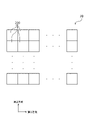
- FIG. 2 is a diagram showing a sparse array provided in the imaging device 2.
- FIG. The imaging device 2 has a pixel array 20 as a light receiving area.
- Pixel array 20 comprises a plurality of pixels 200 .
- the pixels 200 are arranged in an array along the first direction and the second direction, for example.
- the directions are given as an example, and are not limited to the first direction and the second direction. As another non-limiting example, the directions may be 45 degrees offset from the first and second directions, or any other angular offset.
- the pixels 200 are light-receiving pixels, and each pixel 200 may be configured to receive light of a predetermined color.
- the color of the light obtained by the pixel 200 may be, as a non-limiting example, the three primary colors of R (red), G (green), and B (blue).
- at least one of the three colors Cy (cyan), Mg (magenta), and Ye (yellow) may be further provided, and the light intensity of W (white) may be received.
- Colors received by the light-receiving element may be determined by, for example, providing a color filter on the incident surface of the light-receiving element, or providing the light-receiving element with an organic photoelectric conversion film. Also, an infrared cut filter may be used as the filter.
- the analog signal for each color photoelectrically converted by the light receiving element is appropriately converted into a digital signal by an A/D (Analog to Digital) conversion circuit provided inside or outside the imaging element 2.
- a path to the A/D conversion circuit and a circuit forming the A/D conversion circuit may be a circuit equivalent to a general CMOS (Complementary Metal Oxide Semiconductor) sensor, so the details are omitted.
- CMOS Complementary Metal Oxide Semiconductor
- an A/D conversion circuit is provided for each pixel or for each column, and analog signals output from the pixels 200 are appropriately converted into digital signals and output.
- the output digital signal is output to an appropriate circuit through a route equivalent to that of a general circuit.
- FIG. 3 is a diagram showing some pixels 200 extracted from the pixel array 20 according to one embodiment.
- the pixel 200 may be configured to receive light of the same color every four pixels, for example.
- the pixels 200 may be arranged in a Bayer array with these four pixels as a unit.
- they may be arranged in a checkerboard pattern, but the arrangement of colors is not limited to these examples as long as they are appropriately arranged in a mosaic pattern.
- pixels that receive R, pixels that receive G, and pixels that receive B are arranged as illustrated.
- the shaded pixels are light-shielding pixels 202 having a light-shielding structure inside the pixels.
- the light-shielding pixel 202 shields part of the light incident from the incident surface side, receives the light, and converts the intensity of the light in the light-shielded state into an analog signal.
- Other pixels 200 are pixels that photoelectrically convert light received through a color filter or the like, as usual.
- the light-shielded pixels 202 are arranged, for example, so as not to be adjacent to the pixels (8-connected pixels) that are oblique to the top, bottom, left, and right. Also, the light-shielded pixels 202 may be arranged periodically in the pixel array 20 .
- the light-shielding pixel 202 is not included in the group of pixels that receive G light, but it is not limited to this.
- at least one pixel in the pixel group that receives G light may be the light-shielded pixel 202 .
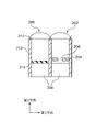
- FIG. 4 is a diagram schematically showing an example of the light-shielded pixel 202.
- the light-shielding pixel 202 includes, for example, a light-shielding film or an absorbing film as a light-shielding structure within the pixel.
- the light-shielding pixel 202 includes a light-shielding film 204 and an aperture 206.
- the light-shielding film 204 (or absorption film) is formed of a film that shields the entire visible light region or light in the wavelength region of the color received by the light-shielding pixel 202 .
- the light-shielding film 204 may be formed of, as non-limiting examples, an appropriate metal, or an organic material such as a color filter having a property of absorbing an appropriate wavelength range.
- the light shielding film 204 is a thin or thick film made of a material equivalent to the light shielding structure used for the dummy pixel. may
- the light-shielding film 204 has openings 206 to limit the area of light incident on the light-receiving elements of the light-shielding pixels 202 .
- the light-shielding pixel 202 photoelectrically converts the light incident through the aperture 206 and outputs an analog signal based on the intensity of the light incident through the aperture 206 .
- the size of the opening 206 formed by the light shielding film 204 may be 25% or less of the area of the light receiving region of the light receiving element.
- the size of the aperture 206 is 25 % size.
- FIG. 5 is an A-A cross-sectional view of the light-shielding pixel 202 shown in FIG. 4 as seen from the second direction. Adjacent pixels 200 are also shown.
- the pixels 200 and the light-shielding pixels 202 each have a light receiving area 208.
- the light-receiving element performs photoelectric conversion according to the intensity of the light incident on the incident surface side of the light-receiving region 208, and outputs an analog signal according to the received intensity.
- the light receiving region 208 is formed of, for example, a photodiode, an organic photoelectric conversion film, or the like.
- the pixels 200 and the light shielding pixels 202 are shielded by the light shielding walls 210.
- the light shielding wall 210 may be, for example, a metal film.
- the light shielding wall 210 is a wall surface for preventing the light incident on the pixel 200 and the light shielding pixel 202 from leaking to the other pixels 200 and the light shielding pixel 202 .
- the surface of the light shielding wall 210 on the pixel 200 side is desirably a reflective surface in order to appropriately acquire the intensity of light incident on the pixel 200 .
- the surface of the light shielding wall 210 on the side of the light shielding pixel 202 is desirably a non-reflecting surface so as not to widen the angle of the light incident on the light shielding pixel 202 .
- the light shielding wall 210 is not limited to this, and since the incidence of the light reflected by the light shielding wall 210 into the opening 206 can be controlled by the optical system, the light shielding wall 210 may also be a reflecting surface on the light shielding pixel 202 side.
- An on-chip lens 212 is provided for each of the pixels 200 and the light-shielding pixels 202 . Via the on-chip lens 212, the pixel 200 and the light-shielding pixel 202 allow light to enter the light receiving area.
- the light shielding film 204 partially prevents light incident through the on-chip lens 212 from entering the light receiving area 208 in the light shielding pixel 202 .
- the solid arrows for pixels 200 and the dotted arrows for light-shielded pixels 202 indicate light incidence from certain angles. Actually, the light is refracted twice at the interface of the on-chip lens 212, but the arrows indicate the directions before and after the on-chip lens 212 to simplify the explanation.
- the light-shielding film 204 as a light-shielding structure in this way, it is possible to limit the incident angle of light incident on the light-receiving region 208 through the opening 206 .
- the incident angle of light incident on the light receiving region of the light-shielding pixel 202 is adjusted to the light receiving region of the pixel 200 in order to sufficiently weaken the intensity of the flare. It can also be 50% or less of the incident angle of the light.
- any suitable incident angle may be obtained based on the arrangement and shape of the opening 206 in the on-chip lens and the light shielding film 204 .
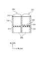
- FIG. 6 is cross-sectional views showing another non-limiting example of the pixel 200 and the shaded pixel 202.
- FIG. As described above, the pixels 200 and the light-shielding pixels 202 receive light in appropriate color wavelength regions using color filters or the like. These figures are examples in which the pixels 200 and the light-shielded pixels 202 are provided with color filters.
- a color filter 214 is provided above the light shielding film 204.
- FIG. 6 the light may already be converted into light limited to a desired wavelength region at the timing of incidence on the opening 206 of the light shielding film 204 .
- the color filter 214 need not be adjacent to the light shielding film 204 as shown in FIG.
- An interlayer insulating film or the like may be provided.
- FIG. 7 is another example in which a color filter 214 is provided above the light shielding film 204.
- a color filter 214 may be provided adjacent to the on-chip lens 212 .
- FIG. 8 shows an example in which a color filter 214 is provided under the light shielding film 204.
- FIG. 8 shows an example in which a color filter 214 is provided under the light shielding film 204.
- FIG. 8 shows an example in which a color filter 214 is provided under the light shielding film 204.
- light passing through openings 206 of light shielding film 204 may enter light receiving region 208 via color filter 214 .
- an interlayer insulating film or the like may be provided between the light shielding film 204 and the color filter 214, as in the case of providing it above the light shielding film 204. Further, an interlayer insulating film or the like may be provided between the color filter 214 and the light receiving region 208.
- FIG. 1 A block diagram illustrating an exemplary computing environment in accordance with the present disclosure.
- FIG. 9 is a diagram showing another example of arrangement of the color filters 214 in the pixels 200 and the light-shielding pixels 202.
- the pixels 200 are provided with color filters 214 so that the light-receiving regions 208 receive light of appropriate colors, while the light-shielding pixels 202 are provided with color filters 214 to receive white light. may not be provided.
- FIG. 10 is a diagram showing another example of the arrangement of filters in the pixel 200 and the light-shielded pixel 202.
- the pixel 200 may comprise a color filter 214 and the shaded pixel 202 may comprise an ND filter 216 (Neutral Density filter).
- ND filter 216 Neutral Density filter
- the light incident angle and the light incident area (incidence intensity) in the light receiving region are smaller (lower) than those of the normal pixel 200, as described above. Therefore, in the light-shielded pixel 202, the light from the light source can be acquired as low-luminance information without performing shutter control, exposure control, or the like. That is, even when there is a light source with high intensity on the display side, by acquiring information from the light-shielding pixels 202, the imaging element 2 can acquire a signal for detecting the shape of this light source. .
- the filter is located below the light shielding film 204 , but it is not limited to this. Also in such a filter configuration, the filter may be above the light shielding film 204 as shown in FIGS.
- FIG. 11 is a diagram showing an example of an image acquired by the imaging device 2 when there is a light source with high intensity on the imaging plane side.
- the hatched area is an area where an image can be properly acquired
- the white area is an area where an image cannot be properly acquired due to flare.
- flare may occur around the position of the light source, as shown in this figure.
- the flare is emphasized for easy understanding, but in reality, the more the position of the light source deviates from the center position, the smaller the influence of the flare may be.
- the influence of flare is reduced by signal processing and image processing.
- the shape of the light source detected by the light-shielded pixels 202 is used to perform correction processing using the PSF.
- FIG. 12 is a diagram showing an example of the shape of the light source detected from the image acquired from the light-shielding pixel 202 when the image of FIG.
- the shape of the light source as shown in FIG. 12 can be detected based on the signal acquired by the light shielding pixel 202.
- the shape of the light source may be detected by binarizing the image signal obtained based on the signal from the light-shielded pixel 202 using a static or dynamic threshold value.
- Fig. 13 is an acquired image of the effect of flare estimated based on the PSF according to the shape of the light source and the light intensity of the light source in Fig. 12.
- the influence of this flare may be obtained, for example, based on the PSF obtained by capturing strong light in advance.
- the influence of flare may be estimated by acquiring information about the PSF and convoluting this PSF information with the light source.
- a neural network model is learned by machine learning using this shape and intensity information and the acquired flare image as training data.
- Machine learning may include any technique, eg, any technique related to deep learning.
- the influence of flare may be inferred based on the shape and intensity information of the light source detected based on the signal output from the light-shielded pixel 202 to this neural network model.
- This neural network model may be a model in which at least one layer is formed by convolutional layers.
- FIG. 14 is a diagram showing an example of an image from which the influence of flare has been removed. For example, by subtracting the image in FIG. 13 from the image in FIG. 11, an image in which the influence of flare is properly removed can be obtained as shown in FIG.
- the shape of the light source can be acquired as white light, and the influence of flare caused by the white light can be removed.
- the color filters 214 may be arranged, for example, so that the color filters 214 provided in the light-shielding pixels 202 form a Bayer array, without being bound by the color of the pixel group to which the light-shielding pixels 202 belong.
- the pixel group of G in FIG. 3 may also be provided with the light-shielding pixel 202, and may be provided with the color filter 214 of the same color as the pixel group to which the light-shielding pixel 202 belongs.
- FIG. 15 is a block diagram schematically showing the imaging element 2 according to one embodiment.
- the imaging device 2 includes the pixel array 20, the storage section 22, the signal processing section 24, and the output section 26 described above. Also, the display 4 is provided with an optical module 40 , but a part of this may be mounted as the imaging device 2 .
- the optical module 40 is a module that includes, for example, an aperture arranged in the material of the display 4 and a module lens, and allows light from the display surface side of the display 4 to enter the pixel array 20 appropriately. Also, the optical module 40 may appropriately include an infrared cut filter or the like.
- a polarizing plate or the like may be provided in the opening.
- the module lens is a lens arranged so that the light transmitted through the aperture is appropriately incident on the pixel array 20, and is provided separately from the on-chip lens 212 described above.
- the pixel array 20 includes, for example, the pixels 200 having the structures shown in FIGS. 3 to 10 and the light-shielding pixels 202 arranged in the array shown in FIG.
- the storage unit 22 is composed of a memory, a storage, etc., which appropriately stores any information that should be stored in the imaging device 2 .
- the signal processing unit 24 is formed by, for example, a signal processing circuit, and appropriately processes and outputs analog signals output from the pixels 200 and the light-shielded pixels 202 .
- the output unit 26 appropriately outputs the signal processed by the signal processing unit 24 to the outside, or stores it in a storage unit provided inside the imaging element.
- the imaging device 2 appropriately includes components necessary for operation, such as a control unit for controlling each configuration of the imaging device 2.
- the signal processing unit 24 includes, for example, an A/D conversion circuit that converts analog signals output from the pixel array 20 into digital signals, and a logic circuit that converts the digital signals into signals suitable for output.
- the analog signals photoelectrically converted in the pixels 200 and the light-shielded pixels 202 of the pixel array 20 are converted into digital signals (digital image signals) by the A/D conversion circuit of the signal processing section 24 and output. If there is no need for signal processing or image processing after this, this digital image signal is output via the output section 26 .
- the image signals output from the light-shielded pixels 202 converted by the A/D conversion circuit are used to detect the shape of the light source.
- the signal processing unit 24 reconstructs a high-brightness image from the thinned image signals obtained from the light-shielded pixels 202 . From this reconstructed image, the shape of the light source is detected using, for example, an arbitrary threshold as described above. In addition to this shape detection, the signal processing section 24 may also detect the light intensity of the light source.
- the signal processing unit 24 that acquires the shape of the light source may perform processing for interpolating pixels at the positions of the light-shielded pixels 202 in the image based on the image signals output from the pixels 200 and the light-shielded pixels 202 .
- This interpolation can use a general defect correction method.
- the signal processing unit 24 calculates the influence of flare or the like based on the shape of the light source obtained from the light-shielded pixels 202. By calculating this effect, the signal processing unit 24 acquires image information indicating the effect of flare or the like as shown in FIG.
- the signal processing unit 24 appropriately subtracts the image information indicating the influence of flare or the like from the image information in which the influence of flare or the like has not been removed, thereby removing the influence of flare or the like shown in FIG. Image information can be acquired.
- the signal processing unit 24 performs other necessary processing to acquire an appropriate image signal. For example, demosaic processing, linear matrix processing, or other processing that makes the data suitable for display may be performed, or processing such as various filter processing may be performed.
- the signal processing unit 24 executes all the processing. detection circuit), a light-shielded pixel correction section (light-shielded pixel correction circuit), and a flare correction section (flare correction circuit). These circuits may be formed of analog or digital circuits as appropriate.
- the digital circuit may be any circuit such as ASIC (Application Specific Integrated Circuit), FPGA (Field-Programmable Gate Array), or the like.
- the present embodiment it is possible to accurately remove the effects of flare and the like on the captured image by providing the light-shielding pixels having the light-shielding structure in the light-receiving pixels. Since the imaging device according to the present embodiment does not require exposure control, double exposure, or the like, it is possible to acquire more appropriate images efficiently.
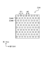
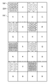
- FIG. 16 is a diagram showing an arrangement example of apertures 206 in light-shielded pixels 202. As shown in FIG. For example, as shown in FIG. 16, each light-shielding pixel 202 may have openings 206 that have the same shape and size, but different positions within the pixel.
- the imaging device 2 can separate the reflected light from the subject and the diffracted light generated in the display 4. It becomes possible.
- FIG. 17 is a diagram showing an arrangement example of apertures 206 in light-shielded pixels 202. As shown in FIG. For example, as shown in FIG. 17, each light-shielding pixel 202 may have apertures 206 that are located at the same position within the pixel and have different sizes.
- the diffracted light in the display 4 influences the received brightness value as the incident angle becomes smaller.
- the incident angle is disturbed by diffraction or the like that occurs in close proximity, whether or not light enters the aperture 206 with a small incident angle varies greatly. Therefore, by providing the apertures 206 with different incident angles, it is possible to analyze the image for each size of the apertures 206 to determine whether the light received by the light-shielding pixels 202 is reflected from the subject or not on the display 4. It is possible to make it easier to determine whether it is diffraction.
- FIG. 18 is a diagram showing still another arrangement example of the apertures 206 in the light-shielded pixels 202. As shown in FIG. As shown in FIG. 18, apertures 206 with different sizes and positions within the pixel may be provided. Also, although the shape is circular, it is not limited to this, and may be any other shape such as a rectangle, an ellipse, or the like.
- the accuracy of flare detection is further improved by appropriately changing the size of the aperture 206 and the relative position within the pixel. It is possible to
- the electronic device 1 is provided with one imaging element 2, but is not limited to this.
- the electronic device 1 may include two or more imaging elements 2.
- FIG. 19 shows an external view of the electronic device 1 according to one embodiment.
- the electronic device 1 includes two imaging elements 2a and 2b. In this way, the imaging element can also be configured with a compound eye.
- the electronic device 1 may include two imaging elements 2a and 2b with different imaging characteristics. Also, the characteristics of the two imaging elements 2a and 2b may be the same.
- the image sensor 2a includes the light-shielded pixels 202 as described above, and the image sensor 2b has the same pixel array configuration as the image sensor 2a. It is good also as a pixel which carries out.
- the configuration of the optical module 40 in FIG. 15 may be changed.
- one may be provided with an infrared cut filter and the other may be configured without an infrared cut filter.
- the imaging elements 2a and 2b may be configured to have polarization filters with different polarization directions.
- the imaging devices 2a and 2b may be configured to include module lenses with different characteristics.
- the accuracy of light source detection in the light-shielded pixels 202 can be improved by using parallax. For example, since diffraction on the display 4 causes a large parallax, it is possible for the signal processing unit 24 to perform correction to reduce the influence of diffraction on the display 4 based on the intensity of light received by the light-shielded pixels 202 .
- the imaging device 2a has a pixel array 20 that includes arrayed pixels 200 and light-shielded pixels 202 along the first direction and the second direction
- the imaging device 2b has the pixel array 20 arranged in the first direction and the second direction.
- a configuration in which the pixels 200 and the light-shielded pixels 202 are arrayed in a direction rotated by 45 degrees with respect to the second direction may be employed.
- the image sensor 2a can acquire information in the direction of the array
- the image sensor 2b can acquire information in a direction rotated 45 degrees from the direction of the array. becomes. Therefore, it is possible to improve the accuracy of detecting the shape of the light source and correcting the defect in the light-shielded pixel 202 .
- the electronic device can also include a plurality of imaging elements. These imaging devices can correct and interpolate mutually output images.
- the light-shielding pixels 202 were formed in the light-shielding film 204, but control of the amount of light in the light-shielding pixels 202 is not limited to this.
- FIG. 20 is a diagram schematically showing the pixel array 20 according to one embodiment.
- the light-shielding pixels 202 hatched in the drawing are each provided with a polarizing element that polarizes light in the direction of the hatched lines.
- the polarizing element may be, for example, a polarizing filter.
- the amount of light can be changed.
- a polarizing element is provided, the influence of flare can be removed with higher accuracy based on the signal obtained by the light-shielding pixel 202 by obtaining the polarization state of the reflected light on the display 4 in advance.
- the light-shielding pixel 202 may be configured to receive light in any other wavelength region such as W.
- the unit of the light-receiving and partially light-shielding region is the pixel unit, but the present invention is not limited to this.
- the pixel 200 divided pixels that share an on-chip lens, a light receiving element, and a pixel circuit may be formed, and a region partially shielded from light may be provided in units of the divided pixels.
- FIG. 21 is a diagram showing an example of a pixel 200 and divided pixels according to one embodiment. Boundaries indicated by solid lines indicate boundaries of pixels, and boundaries indicated by dotted lines indicate churches of divided pixels. As shown in FIG. 21, the pixel 200 includes a plurality of divided pixels 218 and divided light-shielded pixels 220. As shown in FIG. The divided pixel 218 and the divided light-shielded pixel 220 belonging to the same pixel 200 may share the on-chip lens, light receiving element, and pixel circuit as described above.
- FIG. 22 is a cross-sectional view of the portion related to the R pixel extracted from the B-B cross section in FIG. Pixel 200 includes divided pixels 218 and divided shaded pixels 220 .
- the divided pixel 218 is provided with a color filter 214, and the divided light-shielding pixel 220 is further provided with a light-shielding film 204.
- the light receiving regions 208 of the plurality of divided pixels 218 are provided with element isolation films 222 as shown.
- the element isolation film 222 is a layer that isolates the light receiving regions of the divided pixels 218, and is made of metal or insulator, for example.
- a memory area forming a memory area may be provided for each light receiving area 208 .
- the divided light-shielded pixels 220 may be formed by providing the light-shielding films 204 in some of the divided pixels 218 .
- a polarizing element may be provided instead of the light shielding film 204 as described above.
- FIG. 23 is a diagram showing another example of shielding divided pixels.
- the number of divided pixels provided in the pixel 200 is not limited to 2 ⁇ 2, and there may be more divided pixels than 2 ⁇ 1 or 2 ⁇ 2.
- an on-chip lens 212 may be placed for each pixel 200.
- FIG. 24 is a diagram showing another example of shielding divided pixels.
- the pixels 200 and the light-shielded pixels 202 may each constitute divided pixels.
- the divided light-shielded pixels 220 of the light-shielded pixel 202 may each have an aperture 206 .
- a light-shielded region may be provided in the divided pixel as in the present embodiment. It should be noted that, as in the above-described embodiment, the arrangement of colors and the like are given as some non-limiting examples, and the aspects of the present disclosure are not limited to these examples.
- the divided light-shielding pixels 220 may be formed by a polarizing element instead of the light-shielding film 204. FIG.
- the imaging device 2 can detect diffracted light in the display 4.
- the structure is not limited to detection of diffracted light.
- the imaging device 2 As an imaging device for fingerprint authentication, it becomes possible to use the imaging device 2 as an imaging device for fingerprint authentication.
- the image sensor 2 acquires the reflected light of the light emitted from the display 4 on the finger in contact with the cover glass 5, the fingerprint is reproduced using the image signal output from the light-shielded pixel 202 or the divided light-shielded pixel 220. may be configured. Reflected light is diffusely reflected at the locations where the ridges of the fingerprint and the cover glass 5 are in contact, while the angle of incidence and the angle of reflection on the surface of the cover glass 5 coincide with each other in the regions of valleys of the fingerprint. Therefore, by acquiring the intensity of the light received by the light-shielding pixels 202 whose incident angles are limited, it is possible to reconstruct an appropriate fingerprint image.
- the position of the barcode can be set within 10 cm from the display 4 or the like.
- Information about such a subject at a relatively short distance from the display 4 may be reconstructed from information received by the light-shielded pixels 202 .
- the distance is within 10 cm, but depending on the situation, it may be set to any distance such as within 5 cm.
- the electronic device 1 may control macro photography mode, fingerprint authentication mode, barcode reading mode, and the like. This mode may be switched by the user.
- the light source, reading pixels, etc. may be appropriately controlled so as to obtain a fingerprint image based on the output from the light-shielded pixels 202. That is, the signal processing unit 24 may control the pixel values from the signals output from the pixels 200 and the light-shielded pixels 202 so that the fingerprint information can be easily obtained. For example, an image may be constructed by multiplying the signal output from the light-shielded pixel 202 by a gain of 1 or more, and controlling the effect of the signal output from the light-shielded pixel 202 to increase. After reconstructing the fingerprint image, the signal processing unit 24 may perform fingerprint authentication using a general technique.
- the signal processing unit 24 may control image reconstruction so as to increase the influence of the output from the light-shielded pixel 202 .
- the light shielding structure is explained using the light shielding film, the absorbing film, and the polarizing element, but the light shielding structure is not limited to this.
- this embodiment a case will be described in which light-shielded pixels and pixels to which a plasmon filter is applied as pixels other than the light-shielded pixels are used.
- FIG. 25 is a diagram showing an example of a plasmon filter.
- the plasmon filter 224 is formed by arranging holes 224b in a honeycomb pattern in a metal (or any conductor) thin film 224a. With this structure, the plasmon filter 224 generates a plasmon resonance phenomenon based on the aperture size D1 and the pitch a0 of the holes 224b.
- Each hole 224b penetrates the thin film 224a and acts as a waveguide.
- Waveguides generally have a cutoff frequency and a cutoff wavelength defined by a size such as a diameter, and have the property of not propagating light of a frequency lower than that (or a wavelength higher than that).
- the cutoff wavelength of hole 224b depends on the aperture size D1 and pitch a0 of hole 224b. The larger the aperture size D1, the longer the cut-off wavelength, and the smaller D1, the shorter the cut-off wavelength.
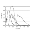
- FIG. 26 is a graph showing transmission wavelengths when the plasmon filter 224 is used.
- a solid line indicates a pitch of 250 nm
- a dashed line indicates a pitch of 325 nm
- a dashed line indicates a pitch of 500 nm.
- the plasmon filter 224 blocks light at the cut-off wavelength and operates in waveguide mode at wavelengths below the cut-off wavelength and in plasmon mode at wavelengths above the cut-off wavelength.
- FIG. 27 is an arrangement example of the plasmon filter 224.
- FIG. As shown in this figure, plasmon filters 224 with different characteristics may be placed in the pixel 200 as in the previous embodiments.
- plasmon filters 224 By providing plasmon filters 224 with different characteristics, it is possible to estimate the light source. For example, light other than the cut-off wavelength in each plasmon filter 224 is received. A light source can be estimated based on this received light.
- the light source can be estimated by calculating the ratio of the signals output from the pixels 200 where the respective plasmon filters 224 are arranged. For example, the color temperature may be estimated based on the outputs of multiple plasmon filters 224 with different characteristics. This estimation is performed by the signal processing unit 24 . Then, the signal processing unit 24 may further calculate the gain for each color filter based on this estimated result, and use the value multiplied by this gain as the value of each color in each pixel.
- FIG. 28 is a diagram showing an example of a pixel in which the plasmon filter 224 and the light-shielding pixel 202 are arranged together. As shown in this figure, a configuration in which a plasmon filter 224 is provided in a pixel different from the light shielded pixel 202 may be employed.
- the use of the plasmon filter 224 also allows the estimation of the light source to be performed as described above. Therefore, when removing flare from the state of the light source, it is possible to more specifically analyze the color components of the flare.
- spoofing can be indicated by referring to the output from the pixel 200 in which the plasmon filter 224 is arranged.
- the reflection of light on living human skin changes significantly around a wavelength of 590 nm.
- the imaging device 2 that acquires multispectral information can be configured. Therefore, it is possible to acquire reflection characteristics at wavelengths around 590 nm in the information acquired as multispectrum.
- the signal processing unit 24 can determine whether or not the subject in contact with the cover glass 5 is a living body. Therefore, the electronic device 1 equipped with the imaging element 2 can perform fingerprint authentication and determine whether or not the fingerprint information is reflected from the living body.
- the plasmon filter 224 may be arranged with respect to the divided pixel 218 when the pixel 200 includes divided pixels.
- the imaging device 2 may be configured to acquire vein information and hemoglobin information instead of fingerprint information. Also, instead of these pieces of information, the imaging device 2 may acquire information on oxygen saturation in blood.
- the image sensor 2 may acquire information on the iris of the human eye.
- the display 4 may be configured to emit light to the extent that it does not damage human eyes.
- the authentication operation using the imaging element 2 may be realized by acquiring one or more pieces of biometric information in the electronic device 1 .
- the electronic device 1 may include a plurality of imaging elements having split pixels as in the fifth embodiment, as in the third embodiment. In such a case, it is possible to interpolate in a form in which the other output of the light-shielded pixel 202 or the divided light-shielded pixel 220 is not light-shielded.
- Other embodiments can be appropriately combined in the same manner.
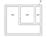
- FIG. 29 is a diagram showing an example of a substrate provided with the imaging element 2.
- FIG. Substrate 30 includes pixel area 300 , control circuitry 302 , and logic circuitry 304 . As shown in FIG. 29, the pixel region 300, the control circuit 302, and the logic circuit 304 may be arranged on the same substrate 30. FIG.
- a pixel region 300 is, for example, a region in which the pixel array 20 and the like described above are provided.
- the pixel circuits and the like described above may be appropriately provided in this pixel region 300 or may be provided in another region (not shown) of the substrate 30 .
- the control circuit 302 has a control section.
- the logic circuit 304 for example, the A/D conversion circuit of the signal processing unit 24 may be provided in the pixel region 300 and the converted digital signal may be output to the logic circuit 304.
- the image processing section (for example, part of the circuit of the signal processing section 24) may be provided in this logic circuit 304.
- FIG. At least part of the signal processing unit 24 and the image processing unit may be mounted not on this chip but on another signal processing chip provided at a location different from the substrate 30, or may be mounted in another processor. may be implemented in
- FIG. 30 is a diagram showing another example of a substrate provided with an imaging device 2.
- a first substrate 32 and a second substrate 34 are provided.
- the first substrate 32 and the second substrate 34 have a laminated structure, and can transmit and receive signals to and from each other appropriately through connection portions such as via holes.
- the first substrate 32 may comprise the pixel area 300 and the control circuit 302, and the second substrate 34 may comprise the logic circuit 304.
- FIG. 31 is a diagram showing another example of a substrate provided with an imaging device 2.
- a first substrate 32 and a second substrate 34 are provided.
- the first substrate 32 and the second substrate 34 have a laminated structure, and signals can be transmitted and received to and from each other appropriately through connection portions such as via holes.
- the first substrate 32 may comprise the pixel area 300 and the second substrate 34 may comprise the control circuit 302 and the logic circuit 304 .
- the storage area may be provided in an arbitrary area.
- a substrate for storage area may be provided, and this substrate may be provided between the first substrate 32 and the second substrate 34 or below the second substrate 34. .
- a plurality of stacked substrates may be connected to each other through via holes as described above, or may be connected by a method such as micro-dumping. These substrates can be laminated by any method such as CoC (Chip on Chip), CoW (Chip on Wafer), or WoW (Wafer on Wafer).
- FIG. 32A and 32B are diagrams showing the internal configuration of a vehicle 360, which is a first application example of the electronic device 1 including the imaging device 2 according to the present disclosure.
- 32A is a view showing the interior of the vehicle 360 from the rear to the front of the vehicle 360
- FIG. 32B is a view showing the interior of the vehicle 360 from the oblique rear to the oblique front of the vehicle 360.
- a vehicle 360 in FIGS. 32A and 32B has a center display 361, a console display 362, a heads-up display 363, a digital rear mirror 364, a steering wheel display 365, and a rear entertainment display 366.
- the center display 361 is arranged on the dashboard 367 at a location facing the driver's seat 368 and the passenger's seat 369.
- FIG. 32 shows an example of a horizontally elongated center display 361 extending from the driver's seat 368 side to the passenger's seat 369 side, but the screen size and location of the center display 361 are arbitrary.
- Information detected by various sensors can be displayed on the center display 361 .
- the center display 361 displays images captured by the image sensor, images of the distance to obstacles in front of and to the side of the vehicle measured by the ToF sensor, and passenger temperatures detected by the infrared sensor. Displayable.
- Center display 361 can be used to display at least one of safety-related information, operation-related information, lifelogs, health-related information, authentication/identification-related information, and entertainment-related information, for example.
- Safety-related information includes information such as the detection of falling asleep, the detection of looking away, the detection of tampering by children riding in the same vehicle, the presence or absence of seatbelt wearing, and the detection of occupants being left behind. It is information detected by The operation-related information uses a sensor to detect a gesture related to the operation of the passenger. Detected gestures may include manipulating various equipment within vehicle 360 . For example, it detects the operation of an air conditioner, a navigation device, an AV device, a lighting device, or the like.
- the lifelog includes lifelogs of all crew members. For example, the lifelog includes a record of each occupant's behavior during the ride.
- the health-related information detects the body temperature of the occupant using a temperature sensor, and infers the health condition of the occupant based on the detected body temperature.
- an image sensor may be used to capture an image of the occupant's face, and the occupant's health condition may be estimated from the captured facial expression.
- an automated voice conversation may be conducted with the passenger, and the health condition of the passenger may be estimated based on the content of the passenger's answers.
- Authentication/identification-related information includes a keyless entry function that performs face authentication using a sensor, and a function that automatically adjusts seat height and position by face recognition.
- the entertainment-related information includes a function of detecting operation information of the AV device by the passenger using a sensor, a function of recognizing the face of the passenger with the sensor, and providing content suitable for the passenger with the AV device.
- the console display 362 can be used, for example, to display lifelog information.
- Console display 362 is located near shift lever 371 on center console 370 between driver's seat 368 and passenger's seat 369 .
- a console display 362 can also display information detected by various sensors.
- the console display 362 may display an image of the surroundings of the vehicle captured by an image sensor, or may display an image of the distance to obstacles around the vehicle.
- the head-up display 363 is virtually displayed behind the windshield 372 in front of the driver's seat 368. Heads-up display 363 can be used to display at least one of safety-related information, operation-related information, lifelogs, health-related information, authentication/identification-related information, and entertainment-related information, for example.
- the heads-up display 363 is often placed virtually in front of the driver's seat 368 and is therefore used to display information directly related to the operation of the vehicle 360, such as vehicle 360 speed and fuel (battery) level. Are suitable.
- the digital rear mirror 364 can display not only the rear of the vehicle 360 but also the state of the passengers in the rear seats. be able to.
- the steering wheel display 365 is arranged near the center of the steering wheel 373 of the vehicle 360.
- Steering wheel display 365 can be used, for example, to display at least one of safety-related information, operational-related information, lifelogs, health-related information, authentication/identification-related information, and entertainment-related information.
- life log information such as the driver's body temperature and information regarding the operation of AV equipment and air conditioning equipment.
- the rear entertainment display 366 is attached to the back side of the driver's seat 368 and passenger's seat 369, and is intended for viewing by passengers in the rear seats.
- Rear entertainment display 366 can be used to display at least one of safety-related information, operation-related information, lifelogs, health-related information, authentication/identification-related information, and entertainment-related information, for example.
- information relevant to the rear seat occupants is displayed. For example, information about the operation of an AV device or an air conditioner may be displayed, or the results obtained by measuring the body temperature of passengers in the rear seats with a temperature sensor may be displayed.
- Optical distance measurement methods are broadly classified into passive and active methods.
- the passive type measures distance by receiving light from an object without projecting light from the sensor to the object.
- Passive types include lens focusing, stereo, and monocular vision.
- the active type measures distance by projecting light onto an object and receiving reflected light from the object with a sensor.
- Active types include an optical radar method, an active stereo method, a photometric stereo method, a moire topography method, an interferometric method, and the like.
- the electronic device 1 according to the present disclosure is applicable to any of these methods of distance measurement.
- the passive or active distance measurement described above can be performed.
- the electronic device 1 including the imaging device 2 according to the present disclosure can be applied not only to various displays used in vehicles, but also to displays mounted on various electronic devices.
- FIG. 33A is a front view of a digital camera 310, which is a second application example of the electronic device 1, and FIG. 33B is a rear view of the digital camera 310.
- FIG. A digital camera 310 in FIGS. 33A and 33B shows an example of a single-lens reflex camera with an interchangeable lens 121, but it is also applicable to a camera in which the lens 121 is not interchangeable.
- FIGS. 33A and 33B In the camera of FIGS. 33A and 33B, when the photographer holds the grip 313 of the camera body 311, looks through the electronic viewfinder 315, determines the composition, adjusts the focus, and presses the shutter, the Captured data is stored in memory.
- a monitor screen 316 for displaying photographed data and the like, a live image and the like, and an electronic viewfinder 315 are provided on the rear side of the camera.
- a sub-screen for displaying setting information such as shutter speed and exposure value is provided on the upper surface of the camera.
- the senor By arranging the sensor on the back side of the monitor screen 316, the electronic viewfinder 315, the sub-screen, etc. used for the camera, it can be used as the electronic device 1 according to the present disclosure.
- the electronic device 1 according to the present disclosure can also be applied to a head-mounted display (hereinafter referred to as HMD).
- HMDs can be used for VR, AR, MR (Mixed Reality), SR (Substitutional Reality), and the like.
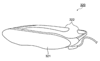
- FIG. 34A is an external view of the HMD 320, which is the third application example of the electronic device 1.
- FIG. The HMD 320 of Figure 34A has a mounting member 322 for mounting over the human eye. This mounting member 322 is fixed by being hooked on a human ear, for example.
- a display device 321 is provided inside the HMD 320 , and the wearer of the HMD 320 can visually recognize a stereoscopic image or the like on the display device 321 .
- the HMD 320 has, for example, a wireless communication function and an acceleration sensor, and can switch stereoscopic images and the like displayed on the display device 321 according to the posture and gestures of the wearer.
- the HMD 320 may be provided with a camera to capture an image of the wearer's surroundings, and the display device 321 may display an image obtained by synthesizing the image captured by the camera and an image generated by a computer.
- a camera is placed on the back side of the display device 321 that is visually recognized by the wearer of the HMD 320, and the area around the wearer's eyes is captured by this camera. By displaying it on the display, people around the wearer can grasp the wearer's facial expressions and eye movements in real time.
- FIG. 34B the electronic device 1 according to the present disclosure can also be applied to smart glasses 340 that display various information on glasses 344.
- FIG. A smart glass 340 in FIG. 34B has a body portion 341, an arm portion 342, and a barrel portion 343.
- Body portion 341 is connected to arm portion 342 .
- the body portion 341 is detachable from the glasses 344 .
- the main unit 341 incorporates a control board for controlling the operation of the smart glasses 340 and a display unit.
- the body portion 341 and the lens barrel are connected to each other via the arm portion 342 .
- the lens barrel portion 343 emits image light emitted from the body portion 341 via the arm portion 342 to the lens 345 side of the glasses 344 .
- This image light enters the human eye through lens 345 .
- the wearer of the smart glasses 340 in FIG. 34B can visually recognize not only the surroundings but also various information emitted from the lens barrel 343 in the same manner as ordinary glasses.
- the electronic device 1 according to the present disclosure can also be applied to a television device (hereinafter referred to as TV).
- TV television device
- Recent TVs tend to have a frame as small as possible from the viewpoint of miniaturization and design. For this reason, when a camera for photographing the viewer is provided on the TV, it is desirable to place the camera on the back side of the display panel 331 of the TV.
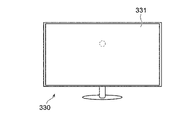
- FIG. 35 is an external view of a TV 330, which is a fourth application example of the electronic device 1.
- the frame of the TV 330 in FIG. 35 is minimized, and almost the entire front side is the display area.
- the TV 330 has a built-in sensor such as a camera for photographing the viewer.
- the sensor in FIG. 35 is arranged behind a portion of the display panel 331 (for example, the portion indicated by the dashed line).
- the sensor may be an image sensor module, and various sensors such as face authentication sensors, distance measurement sensors, and temperature sensors can be applied. may be placed.
- the image sensor module can be arranged overlapping the back side of the display panel 331, so there is no need to arrange a camera or the like in the frame, and the TV 330 can be miniaturized. In addition, there is no fear that the design will be spoiled by the frame.
- FIG. 36 is an external view of a smartphone 350, which is a fifth application example of the electronic device 1.
- the display surface 2z extends close to the external size of the electronic device 1, and the width of the bezel 2y around the display surface 2z is several millimeters or less.
- a front camera is often mounted on the bezel 2y, but in FIG. 36, an image sensor module 9 functioning as a front camera is mounted on the back side of the display surface 2z, for example, in the approximate center, as indicated by the dashed line. are placed.
- a pixel comprising a light-receiving element that photoelectrically converts incident light and outputs an analog signal based on the intensity of the light; a pixel array in which the pixels are arranged in an array; with Some of the pixels belonging to the pixel array have a light shielding structure that shields part of the light incident on the light receiving element. image sensor.
- the light shielding structure limits the angle of incidence of light incident on the light receiving element of the pixel provided with the light shielding structure.
- the light shielding structure is a light shielding film provided in the light receiving element, (2) The imaging device according to the above.
- the light shielding structure is formed so that the size of the opening in the pixel is 25% or less of the surface area of the light receiving element.
- the openings formed by the light shielding structure have the same size or different sizes depending on the pixels.
- the imaging device according to (3) is the same size or different sizes depending on the pixels.
- the apertures formed by the light shielding structures are provided by the pixels at the same or different relative positions in the pixels;
- the imaging device according to (3) or (5) The imaging device according to (3) or (5).
- one or more openings are formed by the light shielding structure;
- the imaging device according to any one of (3) to (6).
- the light shielding structure is a polarizer provided in the light receiving element, (2) The imaging device according to the above.
- the pixels having the light shielding structure are arranged in non-adjacent positions in the pixel array;
- the imaging device according to any one of (2) to (9).
- the pixels having the light shielding structure are arranged periodically in the pixel array; (10) The imaging device according to the above.
- An on-chip lens is provided for each pixel, A module lens is provided in the pixel array, The imaging device according to any one of (2) to (11).
- the pixel includes a divided pixel obtained by dividing the light receiving element belonging to the pixel into a plurality of pixels, the pixel having the light shielding structure has the light shielding structure for at least one of the divided pixels;
- the imaging device according to any one of (2) to (12).
- the signal processing circuit detects the shape of the light source based on the output from the pixel provided with the light shielding structure.
- the imaging device according to the above.
- the signal processing circuit estimates a light source based on the output from the pixel provided with the light shielding structure. (14) The imaging device according to the above.
- an imaging device according to any one of (14) to (17); a display having a display surface for displaying information on the incident surface side of the imaging device; with The imaging element converts light received through the display by photoelectric conversion. Electronics.
- the light shielding structure includes the pixel in which the incident angle at which light can enter is controlled to 50% or less of the normal angle, generating imaging information of a nearby object based on the output from the pixel having the light shielding structure;
- the biometric information is information including any one of fingerprints, iris, veins, skin, hemoglobin, or oxygen saturation, (20) Electronic equipment according to.
- the wiring layout of the display in at least one imaging element is different from the wiring layout of the display in the other imaging elements, The electronic device according to (24).
- 1 Electronics, 1a: display area, 1b: bezel, 2: image sensor, 3: component layer, 4: display, 5: coverslip, 20: pixel array, 200: pixels, 202: shading pixels, 204: light shielding film, 206: Aperture, 208: light receiving area, 210: Shading wall, 212: on-chip lens, 214: color filters, 216: ND filter, 218: division pixel, 220: divided shaded pixels, 222: element isolation film, 224: Plasmon Filter, 224a: thin film, 224b: hole, 22: storage unit, 24: signal processor, 26: output section,
Abstract
>[Problem] To improve image quality. [Solution] This imaging element includes pixels and a pixel array. The pixels each include a light-receiving element that performs photoelectric conversion of incident light and outputs an analog signal based on the intensity of the light. In the pixel array, the pixels are arranged in an array. Some of the pixels that belong to the pixel array include a light-blocking structure that blocks some of the light incident to the light-receiving element. The light-blocking structure limits the incident angle of the light incident to the light-receiving element.
Description
本開示は、撮像素子及び電子機器に関する。
The present disclosure relates to imaging devices and electronic devices.
スマートフォン等のディスプレイを備えるデバイスにおいて、ディスプレイ下にカメラモジュールを配置することが検討されている。このようなカメラモジュールにおいては、ディスプレイ越しに輝度の高い光源を有する環境において撮像をすると、ディスプレイの回折によるフレアが大きな課題となる。このフレアは、PSF(Point Spread Function)補正をすることで補正をすることができるが、光源の形状を知ることでより正確なフレアの補正を実現することができる。
In devices with displays such as smartphones, placing a camera module under the display is being considered. In such a camera module, if an image is captured in an environment with a bright light source through the display, flare due to diffraction of the display becomes a major problem. This flare can be corrected by PSF (Point Spread Function) correction, but knowing the shape of the light source enables more accurate flare correction.
光源の形状を推定するために、超短蓄シャッタで撮像することが行われるが、光源形状がわかるような極端な短蓄画像は、HDR(High Dynamic Range)画像として利用するにはSNR(Signal to Noise Ratio)が悪化することが知られている。また、HDR画像を合成するには、フレームメモリが必要となる場合もあり、フレア処理をセンサに内蔵すると、回路規模の増大を招くという問題もある。短蓄と長蓄で時間差が発生するので、光源形状の検出と通常画像での時間差が発生し、動画撮像時に不利になるという問題もある。
In order to estimate the shape of the light source, an image is taken with an ultra short storage shutter. to Noise Ratio) is known to deteriorate. In addition, a frame memory may be required to synthesize an HDR image, and if flare processing is built into the sensor, there is also the problem of an increase in circuit size. Since a time difference occurs between short-term and long-term storage, there is also a problem that a time difference occurs between the detection of the shape of the light source and the normal image, which is disadvantageous when capturing a moving image.
そこで、本開示では、画質を向上する撮像素子を提供する。
Therefore, the present disclosure provides an imaging device that improves image quality.
一実施形態によれば、撮像素子は、画素と、画素アレイと、を備える。画素は、入射した光を光電変換して、光の強度に基づいたアナログ信号を出力する受光素子を備える。画素アレイは、前記画素がアレイ状に配置される。前記画素アレイに属する一部の前記画素は、前記受光素子に入射する光の一部を遮光する遮光構造を備える。
According to one embodiment, the imaging device includes pixels and a pixel array. A pixel includes a light receiving element that photoelectrically converts incident light and outputs an analog signal based on the intensity of the light. The pixels are arranged in an array in the pixel array. Some of the pixels belonging to the pixel array have a light shielding structure that shields part of the light incident on the light receiving element.
前記遮光構造により、当該遮光構造を備える前記画素の前記受光素子に入射する光の入射角度を制限してもよい。
The light shielding structure may limit the incident angle of light incident on the light receiving element of the pixel provided with the light shielding structure.
前記遮光構造は、前記受光素子の入射面側に備えられる遮光膜であってもよい。
The light shielding structure may be a light shielding film provided on the incident surface side of the light receiving element.
前記遮光構造は、前記画素において、開口のサイズが前記受光素子の表面の面積の25%以下となるように形成されてもよい。
The light shielding structure may be formed so that the size of the aperture in the pixel is 25% or less of the area of the surface of the light receiving element.
前記遮光構造により形成される開口は、前記画素により同一又は異なるサイズであってもよい。
The apertures formed by the light shielding structure may have the same size or different sizes depending on the pixels.
前記遮光構造により形成される開口は、前記画素により前記画素における同一又は異なる相対位置に備えられてもよい。
The apertures formed by the light shielding structures may be provided at the same or different relative positions in the pixels depending on the pixels.
前記画素において、前記遮光構造により1又は複数の開口が形成されてもよい。
In the pixel, one or more openings may be formed by the light shielding structure.
前記遮光構造は、前記受光素子の入射面側に備えられる偏光子であってもよい。
The light shielding structure may be a polarizer provided on the incident surface side of the light receiving element.
前記遮光構造が配置される前記画素とは異なる画素において、前記受光素子の入射面側にプラズモンフィルタが配置される前記画素を備えてもよい。
A pixel different from the pixel where the light shielding structure is arranged may include the pixel where the plasmon filter is arranged on the incident surface side of the light receiving element.
前記遮光構造を有する前記画素は、前記画素アレイにおいて隣接しない位置に配置されてもよい。
The pixels having the light shielding structure may be arranged at non-adjacent positions in the pixel array.
前記遮光構造を有する前記画素は、前記画素アレイにおいて、周期的に配置されてもよい。
The pixels having the light shielding structure may be arranged periodically in the pixel array.
前記画素ごとに、オンチップレンズを備えてもよく、前記画素アレイに、モジュールレンズを備えてもよい。
An on-chip lens may be provided for each pixel, and a module lens may be provided for the pixel array.
前記画素において、当該画素に属する前記受光素子を複数に分割した、分割画素を備えてもよく、前記遮光構造を有する前記画素は、前記分割画素の少なくとも1つについて前記遮光構造を備えてもよい。
The pixel may include divided pixels obtained by dividing the light receiving element belonging to the pixel into a plurality of pixels, and the pixel having the light shielding structure may include the light shielding structure for at least one of the divided pixels. .
前記受光素子から出力されたアナログ信号をデジタル信号に変換する、信号処理回路、をさらに備えてもよい。
A signal processing circuit that converts an analog signal output from the light receiving element into a digital signal may be further provided.
前記信号処理回路は、前記遮光構造が備えられる前記画素からの出力に基づいて、光源の形状を検出してもよい。
The signal processing circuit may detect the shape of the light source based on the output from the pixel provided with the light shielding structure.
前記信号処理回路は、前記光源の形状に基づいて、前記デジタル信号を補正してもよい。
The signal processing circuit may correct the digital signal based on the shape of the light source.
プラズモンフィルタを備える場合に、前記信号処理回路は、前記遮光構造が備えられる前記画素からの出力に基づいて、光源の推定をしてもよい。
When the plasmon filter is provided, the signal processing circuit may estimate the light source based on the output from the pixel provided with the light shielding structure.
一実施形態によれば、電子機器は、上記のいずれかに記載の撮像素子と、前記撮像素子の入射面側に、情報を表示する表示面を有する、ディスプレイと、を備え、前記撮像素子は、前記ディスプレイを介して受光した光を光電変換により変換する。
According to one embodiment, an electronic device includes any one of the above-described imaging devices, and a display having a display surface for displaying information on an incident surface side of the imaging device, wherein the imaging device includes and photoelectrically converting the light received through the display.
前記遮光構造により、光が入射可能な入射角が通常の50%以下に制御された前記画素を備えてもよく、前記遮光構造を有する前記画素からの出力に基づいて、近接する物体の撮像情報を生成してもよい。
The light shielding structure may include the pixel in which the incident angle at which light can be incident is controlled to be 50% or less of a normal incident angle, and based on the output from the pixel having the light shielding structure, imaging information of an adjacent object. may be generated.
前記遮光構造を有する前記画素からの出力に基づいて、前記ディスプレイを介して生体情報を取得してもよい。
Biometric information may be obtained through the display based on the output from the pixel having the light shielding structure.
前記生体情報は、指紋、高裁、静脈、肌、ヘモグロビン、又は、酸素飽和度のうちいずれか1つを含む情報であってもよい。
The biometric information may be information including any one of fingerprints, high blood pressure, veins, skin, hemoglobin, or oxygen saturation.
前記遮光構造を有する前記画素からの出力に基づいて、前記ディスプレイに起因する画質の劣化を復元してもよい。
Deterioration in image quality caused by the display may be restored based on the output from the pixel having the light shielding structure.
前記遮光構造を有する前記画素からの出力に基づいて、バーコードの情報を取得してもよい。
Information of the barcode may be obtained based on the output from the pixel having the light shielding structure.
前記撮像素子を複数備えてもよい。
A plurality of the imaging devices may be provided.
複数の前記撮像素子において、少なくとも1つの前記撮像素子における前記ディスプレイの配線レイアウトが他の前記撮像素子における前記ディスプレイの配線レイアウトと異なっていてもよい。
In the plurality of imaging elements, the wiring layout of the display in at least one imaging element may be different from the wiring layout of the display in the other imaging elements.
以下、図面を参照して本開示における実施形態の説明をする。図面は、説明のために用いるものであり、実際の装置における各部の構成の形状、サイズ、又は、他の構成とのサイズの比等が図に示されている通りである必要はない。また、図面は、簡略化して書かれているため、図に書かれている以外にも実装上必要な構成は、適切に備えるものとする。
Hereinafter, embodiments of the present disclosure will be described with reference to the drawings. The drawings are used for explanation, and it is not necessary that the shapes, sizes, ratios, etc. of the configuration of each part in the actual apparatus are as shown in the drawings. In addition, since the drawings are drawn in a simplified manner, it is assumed that configurations necessary for mounting other than those shown in the drawings are appropriately provided.
(第1実施形態)
図1は、一実施形態に係る電子機器を模式的に示す外観図及び断面図である。電子機器1は、例えば、スマートフォン、携帯電話、タブレット型端末、PC等の表示機能と撮影機能とを兼ね備えた任意の電子機器である。電子機器1は、これらの例に限定されるものではなく、例えば、カメラ等の撮像装置、医療機器、検査装置等の他のデバイスであってもよい。図に示すように、便宜的に、第1方向、第2方向及び第3方向と定義する。電子機器1は、撮像素子2と、部品層3と、ディスプレイ4と、カバーガラス5と、を備える。 (First embodiment)
FIG. 1 is an external view and a cross-sectional view schematically showing an electronic device according to an embodiment. Theelectronic device 1 is any electronic device having both a display function and a photographing function, such as a smart phone, a mobile phone, a tablet terminal, or a PC. The electronic device 1 is not limited to these examples, and may be other devices such as imaging devices such as cameras, medical devices, and inspection devices. As shown in the figure, for convenience, they are defined as a first direction, a second direction and a third direction. An electronic device 1 includes an imaging device 2, a component layer 3, a display 4, and a cover glass 5.
図1は、一実施形態に係る電子機器を模式的に示す外観図及び断面図である。電子機器1は、例えば、スマートフォン、携帯電話、タブレット型端末、PC等の表示機能と撮影機能とを兼ね備えた任意の電子機器である。電子機器1は、これらの例に限定されるものではなく、例えば、カメラ等の撮像装置、医療機器、検査装置等の他のデバイスであってもよい。図に示すように、便宜的に、第1方向、第2方向及び第3方向と定義する。電子機器1は、撮像素子2と、部品層3と、ディスプレイ4と、カバーガラス5と、を備える。 (First embodiment)
FIG. 1 is an external view and a cross-sectional view schematically showing an electronic device according to an embodiment. The
以下、この図1に示すように、ディスプレイ4の第3方向において負側を、アンダーディスプレイと記載することがある。例えば、撮像素子2をアンダーディスプレイの撮像素子と記載することがある。
Hereinafter, as shown in FIG. 1, the negative side of the display 4 in the third direction may be referred to as under display. For example, the imaging element 2 may be described as an under-display imaging element.
電子機器1は、例えば、外観図に示すように、表示領域1aと、ベゼル1bと、を備える。電子機器1は、画像、映像等(以下、画像等と記載することがある。)をこの表示領域1aに表示させる。ベゼル1bは、ディスプレイ表示面側における画像を取得するべく、所謂インカメラが備えられることがあるが、今日においては、このベゼル1bの占有する領域を狭くすることが求められていることが多い。このため、本実施形態に係る電子機器1は、アンダーディスプレイに撮像素子2を備え、ベゼル1bが表示面側で占有する領域を狭めている。
The electronic device 1 includes, for example, a display area 1a and a bezel 1b, as shown in the external view. The electronic device 1 displays an image, video, etc. (hereinafter sometimes referred to as an image, etc.) in the display area 1a. The bezel 1b is sometimes provided with a so-called in-camera to acquire an image on the display screen side, but nowadays, it is often required to narrow the area occupied by the bezel 1b. For this reason, the electronic device 1 according to the present embodiment includes the imaging device 2 in the under display, and the area occupied by the bezel 1b on the display surface side is narrowed.
撮像素子2は、受光素子及び受光素子が出力する信号について信号処理を実行する信号処理回路を備える。撮像素子2は、受光素子が受光した光に基づいて、画像に関する情報を取得する。撮像素子2は、例えば、複数の層から形成される半導体により実装されてもよい。撮像素子2の詳細については、後述する。なお、図においては、撮像素子2は、円の形状を有しているが、撮像素子2の形状は、このような形状に限定されるものではない。限定されない他の形状の例として、矩形が挙げられるが、この他の任意の形状であってもよい。
The imaging element 2 includes a light receiving element and a signal processing circuit that performs signal processing on the signal output by the light receiving element. The imaging element 2 acquires information about an image based on the light received by the light receiving element. The imaging element 2 may be mounted, for example, by a semiconductor formed from multiple layers. Details of the imaging device 2 will be described later. In the drawing, the imaging element 2 has a circular shape, but the shape of the imaging element 2 is not limited to such a shape. Other non-limiting examples of shapes include a rectangle, but may be any other shape.
部品層3は、撮像素子2が属する層である。この部品層3には、例えば、電子機器1において撮像以外の処理を実現するための種々のモジュール、デバイス等が備えられる。
The component layer 3 is the layer to which the imaging device 2 belongs. The component layer 3 includes, for example, various modules, devices, and the like for realizing processing other than imaging in the electronic device 1 .
ディスプレイ4は、画像等を出力するディスプレイであり、断面図に示すように、ディスプレイ4の裏面側に撮像素子2及び部品層3が備えられる。又、撮像素子2は、図に示すようにディスプレイ4に埋め込まれるように備えられる。
The display 4 is a display that outputs images and the like, and as shown in the cross-sectional view, the display 4 has an imaging device 2 and a component layer 3 on the back side thereof. Also, the imaging element 2 is provided so as to be embedded in the display 4 as shown in the figure.
カバーガラス5は、ディスプレイ4を保護するガラス層である。ディスプレイ4とカバーガラス5の間には、ディスプレイ4から出力される光が適切にユーザにとって見やすくなるように偏光層等が備えられていてもよいし、表示領域1aをタッチパネルとして用いることができるように、任意の形式(電圧式、静電式)等のタッチパネルとして動作する層を備えていてもよい。これらの他にも、ディスプレイ4とカバーガラス5との間には、適切に撮像素子2における撮影とディスプレイ4における表示をする形態において任意の層等が備えられていてもよい。
The cover glass 5 is a glass layer that protects the display 4. A polarizing layer or the like may be provided between the display 4 and the cover glass 5 so that the light output from the display 4 can be appropriately viewed by the user, and the display area 1a can be used as a touch panel. In addition, a layer that operates as a touch panel of any type (voltage type, electrostatic type) or the like may be provided. In addition to these, an arbitrary layer or the like may be provided between the display 4 and the cover glass 5 in a form in which the imaging device 2 and the display 4 appropriately capture images.
以下の説明において、半導体層等における受光素子、レンズ、回路等の具体的な実装については、本開示において本質的な構成ではないので説明しないが、図面、説明等から読み取れる形状、構成等に任意の手法を用いて実装できるものである。例えば、撮像素子の制御、信号の取得等は、特に記載の無い限り任意の手法で実現することが可能である。
In the following description, the specific implementation of light receiving elements, lenses, circuits, etc. in semiconductor layers etc. is not described because it is not an essential configuration in the present disclosure, but any shape, configuration, etc. that can be read from the drawings, descriptions, etc. It can be implemented using the method of For example, control of the imaging device, acquisition of signals, and the like can be realized by any method unless otherwise specified.
図2は、撮像素子2に備えられるが疎アレイを示す図である。撮像素子2は、受光する領域として画素アレイ20を備える。画素アレイ20は、複数の画素200を備える。画素200は、例えば、第1方向及び第2方向に沿ってアレイ状に備えられる。なお、方向は、一例として挙げたものであり、第1方向及び第2方向に限定されるものではない。限定されない別の例として、第1方向及び第2方向から45度ずれた方向であってもよいし、その他の任意の角度ずれた方向であってもよい。
FIG. 2 is a diagram showing a sparse array provided in the imaging device 2. FIG. The imaging device 2 has a pixel array 20 as a light receiving area. Pixel array 20 comprises a plurality of pixels 200 . The pixels 200 are arranged in an array along the first direction and the second direction, for example. Note that the directions are given as an example, and are not limited to the first direction and the second direction. As another non-limiting example, the directions may be 45 degrees offset from the first and second directions, or any other angular offset.
この画素200は、受光画素であり、それぞれの画素200において所定の色の光を受光する構成であってもよい。画素200において取得される光の色は、限定されない一例として、R(赤)、G(緑)、B(青)の3原色で示される色であってもよい。別の限定されない一例としては、Cy(シアン)、Mg(マゼンダ)、Ye(イエロー)の3色のうち少なくとも1色をさらに備えていてもよいし、W(白)の光の強度を受光する画素200があってもよい。受光素子において受光される色は、例えば、受光素子の入射面上にカラーフィルタを備えたり、受光素子が有機光電変換膜を備えていたりしてもよい。また、フィルタとして赤外線カットフィルタを用いてもよい。
The pixels 200 are light-receiving pixels, and each pixel 200 may be configured to receive light of a predetermined color. The color of the light obtained by the pixel 200 may be, as a non-limiting example, the three primary colors of R (red), G (green), and B (blue). As another non-limiting example, at least one of the three colors Cy (cyan), Mg (magenta), and Ye (yellow) may be further provided, and the light intensity of W (white) may be received. There may be 200 pixels. Colors received by the light-receiving element may be determined by, for example, providing a color filter on the incident surface of the light-receiving element, or providing the light-receiving element with an organic photoelectric conversion film. Also, an infrared cut filter may be used as the filter.
画素200において、受光素子が光電変換した色ごとのアナログ信号は、撮像素子2の内部又は外部に備えられるA/D(Analog to Digital)変換回路により、適切にデジタル信号に変換される。このA/D変換回路までの経路及びA/D変換回路を構成する回路は、一般的なCMOS(Complementary Metal Oxide Semiconductor)センサと同等の回路であってもよいので、詳細については省略する。例えば、画素ごと、又は、カラムごとにA/D変換回路が備えられ、画素200が出力したアナログ信号は、適切にデジタル信号へと変換されて出力される。また、出力されたデジタル信号についても、一般的な回路と同等な経路で適切な回路へと出力される。
In the pixel 200, the analog signal for each color photoelectrically converted by the light receiving element is appropriately converted into a digital signal by an A/D (Analog to Digital) conversion circuit provided inside or outside the imaging element 2. A path to the A/D conversion circuit and a circuit forming the A/D conversion circuit may be a circuit equivalent to a general CMOS (Complementary Metal Oxide Semiconductor) sensor, so the details are omitted. For example, an A/D conversion circuit is provided for each pixel or for each column, and analog signals output from the pixels 200 are appropriately converted into digital signals and output. Also, the output digital signal is output to an appropriate circuit through a route equivalent to that of a general circuit.
図3は、一実施形態に係る画素アレイ20から、いくつかの画素200を抜き出して示す図である。この図3に示すように、画素200は、例えば、4画素ごとに同じ色の受光をする形態であってもよい。この4画素を単位として、画素200は、限定されない一例として、ベイヤ配列で並べられてもよい。他の例としては、市松模様状に並べられてもよいが、色の配置は、適切にモザイク状に配置されるのであれば、これらの例に限定されるものではない。
FIG. 3 is a diagram showing some pixels 200 extracted from the pixel array 20 according to one embodiment. As shown in FIG. 3, the pixel 200 may be configured to receive light of the same color every four pixels, for example. As a non-limiting example, the pixels 200 may be arranged in a Bayer array with these four pixels as a unit. As another example, they may be arranged in a checkerboard pattern, but the arrangement of colors is not limited to these examples as long as they are appropriately arranged in a mosaic pattern.
画素200は、2 × 2のRを受光する画素、Gを受光する画素、Bを受光する画素が図示するように配置される。斜線で示されている画素は、画素内に遮光構造を有する遮光画素202である。この遮光画素202は、入射面側から入射する光の一部を遮光して光を受光し、この遮光された状態の光の強度をアナログ信号へと変換する。他の画素200は、通常通り、カラーフィルタ等を介して受光した光を光電変換する画素である。
In the pixel 200, 2 × 2 pixels that receive R, pixels that receive G, and pixels that receive B are arranged as illustrated. The shaded pixels are light-shielding pixels 202 having a light-shielding structure inside the pixels. The light-shielding pixel 202 shields part of the light incident from the incident surface side, receives the light, and converts the intensity of the light in the light-shielded state into an analog signal. Other pixels 200 are pixels that photoelectrically convert light received through a color filter or the like, as usual.
この遮光画素202は、例えば、上下左右斜めにある画素(8連結の画素)に隣接しないように配置される。また、この遮光画素202は、画素アレイ20において周期的に配置されていてもよい。
The light-shielded pixels 202 are arranged, for example, so as not to be adjacent to the pixels (8-connected pixels) that are oblique to the top, bottom, left, and right. Also, the light-shielded pixels 202 may be arranged periodically in the pixel array 20 .
なお、図3においては、Gの受光をする画素群に遮光画素202が含まれていないが、これに限定されるものではない。例えば、Gの受光をする画素群の少なくとも1つの画素を遮光画素202としてもよい。
Note that in FIG. 3, the light-shielding pixel 202 is not included in the group of pixels that receive G light, but it is not limited to this. For example, at least one pixel in the pixel group that receives G light may be the light-shielded pixel 202 .
図4は、遮光画素202の一例を模式的に示す図である。遮光画素202は、例えば、画素内に、遮光構造として、遮光膜、又は、吸収膜を備える。この図4における例では、遮光画素202は、遮光膜204と、開口206と、を備える。
FIG. 4 is a diagram schematically showing an example of the light-shielded pixel 202. FIG. The light-shielding pixel 202 includes, for example, a light-shielding film or an absorbing film as a light-shielding structure within the pixel. In the example in FIG. 4, the light-shielding pixel 202 includes a light-shielding film 204 and an aperture 206. In FIG.
この遮光膜204(又は吸収膜)は、可視光領域全て、又は、遮光画素202において受光する色の波長領域の光を遮光する膜で形成される。例えば、遮光膜204は、限定されない例として、適切な金属、又は、適切な波長領域を吸収する特性を有するカラーフィルタ等の有機物により形成されてもよい。遮光膜204は、例えば、画素アレイ20において暗領域の信号を取得するためのダミー画素がある場合には、このダミー画素に用いられる遮光構造と同等の物質から構成される薄膜又は厚膜であってもよい。
The light-shielding film 204 (or absorption film) is formed of a film that shields the entire visible light region or light in the wavelength region of the color received by the light-shielding pixel 202 . For example, the light-shielding film 204 may be formed of, as non-limiting examples, an appropriate metal, or an organic material such as a color filter having a property of absorbing an appropriate wavelength range. For example, if the pixel array 20 has a dummy pixel for obtaining a signal in a dark region, the light shielding film 204 is a thin or thick film made of a material equivalent to the light shielding structure used for the dummy pixel. may
遮光膜204は、開口206を備え、遮光画素202の受光素子に入射する光の領域を制限する。遮光画素202においては、この開口206を介して入射される光を光電変換し、この開口206を介して入射された光の強度に基づいてアナログ信号を出力する。
The light-shielding film 204 has openings 206 to limit the area of light incident on the light-receiving elements of the light-shielding pixels 202 . The light-shielding pixel 202 photoelectrically converts the light incident through the aperture 206 and outputs an analog signal based on the intensity of the light incident through the aperture 206 .
限定されない一例として、遮光膜204により形成される開口206のサイズは、受光素子の受光領域の面積の25%以下としてもよい。例えば、遮光画素202において、第1方向及び第2方向に受光領域の受光面を1 / 2ずつにした矩形の開口206が遮光膜204により形成される場合に、開口206のサイズが、この25%のサイズとなる。
As a non-limiting example, the size of the opening 206 formed by the light shielding film 204 may be 25% or less of the area of the light receiving region of the light receiving element. For example, in the light-shielding pixel 202, when the light-shielding film 204 forms a rectangular aperture 206 in which the light-receiving surface of the light-receiving region is halved in the first direction and the second direction, the size of the aperture 206 is 25 % size.
図5は、図4に示される遮光画素202を第2方向から見たA-A断面図である。隣接する画素200についても図示している。
FIG. 5 is an A-A cross-sectional view of the light-shielding pixel 202 shown in FIG. 4 as seen from the second direction. Adjacent pixels 200 are also shown.
画素200及び遮光画素202は、それぞれに受光領域208を備える。この受光領域208の入射面側に入射された光の強度に応じて、受光素子が光電変換を実行し、受光した強度に応じたアナログ信号を出力する。受光領域208は、例えば、フォトダイオード、有機光電変換膜等により形成される。
The pixels 200 and the light-shielding pixels 202 each have a light receiving area 208. The light-receiving element performs photoelectric conversion according to the intensity of the light incident on the incident surface side of the light-receiving region 208, and outputs an analog signal according to the received intensity. The light receiving region 208 is formed of, for example, a photodiode, an organic photoelectric conversion film, or the like.
画素200、遮光画素202は、遮光壁210により遮蔽される。遮光壁210は、例えば、金属膜であってもよい。遮光壁210は、画素200、遮光画素202に入射した光が他の画素200、遮光画素202に漏れ出さないようにするための壁面である。一例として、遮光壁210の画素200側の面は、画素200に入射する光の強度を適切に取得するため、反射する面であるのが望ましい。逆に、遮光壁210の遮光画素202側の面は、遮光画素202に入射する光の角度を広げないために反射しない面であるのが望ましい。これには限られず、遮光壁210により反射した光の開口206への入射は、光学系により制御できるので、遮光画素202側においても遮光壁210は、反射する面であってもよい。
The pixels 200 and the light shielding pixels 202 are shielded by the light shielding walls 210. The light shielding wall 210 may be, for example, a metal film. The light shielding wall 210 is a wall surface for preventing the light incident on the pixel 200 and the light shielding pixel 202 from leaking to the other pixels 200 and the light shielding pixel 202 . As an example, the surface of the light shielding wall 210 on the pixel 200 side is desirably a reflective surface in order to appropriately acquire the intensity of light incident on the pixel 200 . Conversely, the surface of the light shielding wall 210 on the side of the light shielding pixel 202 is desirably a non-reflecting surface so as not to widen the angle of the light incident on the light shielding pixel 202 . The light shielding wall 210 is not limited to this, and since the incidence of the light reflected by the light shielding wall 210 into the opening 206 can be controlled by the optical system, the light shielding wall 210 may also be a reflecting surface on the light shielding pixel 202 side.
画素200、遮光画素202のそれぞれには、オンチップレンズ212が備えられる。オンチップレンズ212を介して、画素200、遮光画素202は、受光領域に光を入射させる。
An on-chip lens 212 is provided for each of the pixels 200 and the light-shielding pixels 202 . Via the on-chip lens 212, the pixel 200 and the light-shielding pixel 202 allow light to enter the light receiving area.
遮光膜204は、図に示すように、遮光画素202において、オンチップレンズ212を介して入射される光が受光領域208に入射するのを部分的に妨げる。画素200に対する実線の矢印及び遮光画素202に対する点線の矢印は、ある角度からの光の入射を示す。実際にはオンチップレンズ212の境界面において2回屈折するが、説明を簡単にするため、オンチップレンズ212の透過前と透過後の方向を矢印にて示している。
As shown in the drawing, the light shielding film 204 partially prevents light incident through the on-chip lens 212 from entering the light receiving area 208 in the light shielding pixel 202 . The solid arrows for pixels 200 and the dotted arrows for light-shielded pixels 202 indicate light incidence from certain angles. Actually, the light is refracted twice at the interface of the on-chip lens 212, but the arrows indicate the directions before and after the on-chip lens 212 to simplify the explanation.
例えば、図に示すように、画素200においては実線で示される角度で入射された光は、オンチップレンズ212により屈折され、受光領域208に入射する。一方で、遮光画素202においては、同じ角度で同じオンチップレンズ212の位置に入射する光であっても、点線で示すように遮光膜204により遮光され、受光領域208には入射しない。
For example, as shown in the figure, light incident on the pixel 200 at an angle indicated by a solid line is refracted by the on-chip lens 212 and enters the light receiving region 208 . On the other hand, in the light-shielding pixel 202, even if the light is incident on the same position of the on-chip lens 212 at the same angle, it is shielded by the light-shielding film 204 as indicated by the dotted line and does not enter the light-receiving region 208. FIG.
このように、遮光膜204を遮光構造として用いることにより、開口206を介して受光領域208に入射する光の入射角度を制限することが可能となる。限定されない一例として、ディスプレイ等に起因するフレアが発生する場合には、そのフレアの強度を十分に弱めるため、遮光画素202における受光領域に入射する光の入射角度を、画素200における受光領域に入射する光の入射角度の50%以下とすることもできる。この他、オンチップレンズ及び遮光膜204における開口206の配置及び形状に基づいて適切な任意の入射角度となるようにしてもよい。
By using the light-shielding film 204 as a light-shielding structure in this way, it is possible to limit the incident angle of light incident on the light-receiving region 208 through the opening 206 . As a non-limiting example, when flare occurs due to a display or the like, the incident angle of light incident on the light receiving region of the light-shielding pixel 202 is adjusted to the light receiving region of the pixel 200 in order to sufficiently weaken the intensity of the flare. It can also be 50% or less of the incident angle of the light. In addition, any suitable incident angle may be obtained based on the arrangement and shape of the opening 206 in the on-chip lens and the light shielding film 204 .
図6、図7及び図8は、画素200及び遮光画素202の限定されない別の例を示す断面図である。上述したように、画素200及び遮光画素202においては、カラーフィルタ等を用いて適切な色の波長領域についての光を受光する。これらの図は、画素200及び遮光画素202にカラーフィルタを備える例である。
6, 7 and 8 are cross-sectional views showing another non-limiting example of the pixel 200 and the shaded pixel 202. FIG. As described above, the pixels 200 and the light-shielding pixels 202 receive light in appropriate color wavelength regions using color filters or the like. These figures are examples in which the pixels 200 and the light-shielded pixels 202 are provided with color filters.
図6は、遮光膜204の上部にカラーフィルタ214を備えている。このように、遮光膜204の開口206に入射するタイミングにおいて、すでに所望の波長領域に限定された光に変換されていてもよい。なお、遮光膜204の上部にカラーフィルタ214が備えられる場合においては、カラーフィルタ214は、図6に示すように遮光膜204に隣接している必要は無く、遮光膜204との間に適切な層間絶縁膜等を備えていてもよい。
In FIG. 6, a color filter 214 is provided above the light shielding film 204. FIG. In this manner, the light may already be converted into light limited to a desired wavelength region at the timing of incidence on the opening 206 of the light shielding film 204 . When the color filter 214 is provided above the light shielding film 204, the color filter 214 need not be adjacent to the light shielding film 204 as shown in FIG. An interlayer insulating film or the like may be provided.
図7は、遮光膜204の上部にカラーフィルタ214を備える別の例である。この図に示すように、カラーフィルタ214は、オンチップレンズ212に隣接するように備えられていてもよい。
FIG. 7 is another example in which a color filter 214 is provided above the light shielding film 204. FIG. As shown in this figure, a color filter 214 may be provided adjacent to the on-chip lens 212 .
図8は、遮光膜204の下部にカラーフィルタ214を備える例である。この図に示すように、遮光膜204の開口206を透過した光が、カラーフィルタ214を介して受光領域208へと入射する形態であってもよい。
FIG. 8 shows an example in which a color filter 214 is provided under the light shielding film 204. FIG. As shown in this figure, light passing through openings 206 of light shielding film 204 may enter light receiving region 208 via color filter 214 .
遮光膜204の下部にカラーフィルタ214を備える形態の場合も上部に備える場合と同様に、遮光膜204とカラーフィルタ214との間に層間絶縁膜等が備えられていてもよい。また、カラーフィルタ214と受光領域208との間に層間絶縁膜等が備えられる構成であってもよい。
In the case of providing the color filter 214 below the light shielding film 204, an interlayer insulating film or the like may be provided between the light shielding film 204 and the color filter 214, as in the case of providing it above the light shielding film 204. Further, an interlayer insulating film or the like may be provided between the color filter 214 and the light receiving region 208. FIG.
図9は、画素200と遮光画素202におけるカラーフィルタ214の配置の別の例を示す図である。この図に示すように、画素200においては、受光領域208に適切な色の光を受光するように、カラーフィルタ214が備えられる一方で、遮光画素202においては、白色光を受光するべくカラーフィルタが備えられない形態としてもよい。
FIG. 9 is a diagram showing another example of arrangement of the color filters 214 in the pixels 200 and the light-shielding pixels 202. FIG. As shown in this figure, the pixels 200 are provided with color filters 214 so that the light-receiving regions 208 receive light of appropriate colors, while the light-shielding pixels 202 are provided with color filters 214 to receive white light. may not be provided.
図10は、画素200と遮光画素202におけるフィルタの配置の別の例を示す図である。画素200は、カラーフィルタ214を備え、遮光画素202は、NDフィルタ216(Neutral Densityフィルタ)を備えてもよい。NDフィルタ216を備えることにより、遮光画素202における入射光の入射角度の制限を与えるとともに、入射光の強度をより適切に制御することも可能となる。このように、開口206のサイズだけではなく、NDフィルタ216により受光強度を制御してもよい。
FIG. 10 is a diagram showing another example of the arrangement of filters in the pixel 200 and the light-shielded pixel 202. FIG. The pixel 200 may comprise a color filter 214 and the shaded pixel 202 may comprise an ND filter 216 (Neutral Density filter). By providing the ND filter 216, it becomes possible to limit the incident angle of the incident light in the light-shielding pixel 202 and to control the intensity of the incident light more appropriately. In this way, the received light intensity may be controlled not only by the size of the aperture 206 but also by the ND filter 216. FIG.
遮光画素202においては、上述のように光の入射角及び受光領域における光の入射面積(入射強度)を通常の画素200と比較して小さく(低く)している。このため、遮光画素202においては、シャッター制御、露光制御等をすることなく、光源からの光を低輝度の情報として取得することができる。すなわち、ディスプレイ側に強度の高い光源がある場合においても、遮光画素202からの情報を取得することで、撮像素子2は、この光源の形状を検出するための信号を取得することが可能となる。
In the light-shielding pixel 202, the light incident angle and the light incident area (incidence intensity) in the light receiving region are smaller (lower) than those of the normal pixel 200, as described above. Therefore, in the light-shielded pixel 202, the light from the light source can be acquired as low-luminance information without performing shutter control, exposure control, or the like. That is, even when there is a light source with high intensity on the display side, by acquiring information from the light-shielding pixels 202, the imaging element 2 can acquire a signal for detecting the shape of this light source. .
図8から図10においては、フィルタが遮光膜204よりも下側にある場合を用いて説明したが、これに限定されるものではない。このようなフィルタの構成においても、図5から図7に示されるように、フィルタが遮光膜204よりも上側にあってもよい。
8 to 10, the case where the filter is located below the light shielding film 204 has been described, but it is not limited to this. Also in such a filter configuration, the filter may be above the light shielding film 204 as shown in FIGS.
図11は、撮像素子2において、撮影面側に強度の高い光源がある場合に取得した画像の一例を示す図である。斜線領域は、適切に画像が取得できている領域であり、白抜きされている領域は、フレアにより適切に画像が取得できていない領域である。撮影面側(例えば、図1におけるディスプレイ4側)に強度の高い光源がある場合、この図に示すように、当該光源の位置を中心にフレアが発生することがある。図ではわかりやすいようにフレアを強調しているが、実際には光源の中心位置からずれるほどフレアの影響が小さくなることもある。
FIG. 11 is a diagram showing an example of an image acquired by the imaging device 2 when there is a light source with high intensity on the imaging plane side. The hatched area is an area where an image can be properly acquired, and the white area is an area where an image cannot be properly acquired due to flare. When there is a high-intensity light source on the imaging plane side (for example, on the display 4 side in FIG. 1), flare may occur around the position of the light source, as shown in this figure. In the figure, the flare is emphasized for easy understanding, but in reality, the more the position of the light source deviates from the center position, the smaller the influence of the flare may be.
このような場合には、適切に画像が取得できないので、信号処理又は画像処理でフレアの影響を小さくすることが望ましい。そこで、遮光画素202から取得された光源の形状に基づいて、フレアの影響を信号処理及び画像処理により低減させる。具体的には、遮光画素202により検出された光源の形状を用いてPSFによる補正処理を行う。
In such cases, an image cannot be obtained properly, so it is desirable to reduce the influence of flare by signal processing or image processing. Therefore, based on the shape of the light source acquired from the light-shielded pixels 202, the influence of flare is reduced by signal processing and image processing. Specifically, the shape of the light source detected by the light-shielded pixels 202 is used to perform correction processing using the PSF.
図12は、撮像素子2において図11の画像を取得した場合の遮光画素202から取得した画像から検出された光源の形状の一例を示す図である。遮光画素202においては、受光素子に入射する光の強度を制限することにより、強度の高い光源からの光を受光し、物体等との他の反射光の受光の影響をあまり受けなくすることができる。このため、遮光画素202が取得した信号に基づいて、図12に示すような光源の形状を検出することができる。例えば、遮光画素202からの信号に基づいて取得された画像信号において、静的な又は動的なしきい値を用いて2値化することで光源の形状を検出してもよい。
FIG. 12 is a diagram showing an example of the shape of the light source detected from the image acquired from the light-shielding pixel 202 when the image of FIG. In the light-shielding pixel 202, by limiting the intensity of light incident on the light-receiving element, it is possible to receive light from a high-intensity light source and reduce the influence of other reflected light received from an object or the like. can. Therefore, the shape of the light source as shown in FIG. 12 can be detected based on the signal acquired by the light shielding pixel 202. In FIG. For example, the shape of the light source may be detected by binarizing the image signal obtained based on the signal from the light-shielded pixel 202 using a static or dynamic threshold value.
図13は、図12の光源の形状及び光源の光の強度に合わせてPSFに基づいて推定されたフレアの影響を取得した画像である。このフレアの影響は、例えば、事前に強い強度の光を撮影しておくことにより取得されたPSFに基づいて取得されてもよい。例えば、PSFに関する情報を取得しておき、このPSFの情報と、光源との畳み込み積分をすることでフレアの影響を推定してもよい。
Fig. 13 is an acquired image of the effect of flare estimated based on the PSF according to the shape of the light source and the light intensity of the light source in Fig. 12. The influence of this flare may be obtained, for example, based on the PSF obtained by capturing strong light in advance. For example, the influence of flare may be estimated by acquiring information about the PSF and convoluting this PSF information with the light source.
別の例として、種々の形状、強度である強い光源を種々の環境により撮影し、この形状、強度情報と、取得したフレアの画像とを教師データとして機械学習によりニューラルネットワークモデルの学習をしてもよい。機械学習は、任意の手法、例えば、ディープラーニングに関する任意の手法を含んでもよい。そして、このニューラルネットワークモデルに遮光画素202から出力される信号に基づいて検出された光源の形状と強度情報とに基づいて、フレアの影響を推論してもよい。このニューラルネットワークモデルは、少なくとも1層が畳み込み層により形成されるモデルであってもよい。ニューラルネットワークモデルを用いる場合には、フレアの影響の他に、同様の状況下で発生しうるゴーストの影響を補正してもよい。
As another example, strong light sources with various shapes and intensities are photographed in various environments, and a neural network model is learned by machine learning using this shape and intensity information and the acquired flare image as training data. good too. Machine learning may include any technique, eg, any technique related to deep learning. Then, the influence of flare may be inferred based on the shape and intensity information of the light source detected based on the signal output from the light-shielded pixel 202 to this neural network model. This neural network model may be a model in which at least one layer is formed by convolutional layers. When using a neural network model, in addition to flare effects, ghost effects that may occur under similar circumstances may be corrected.
図14は、フレアの影響を取り除いた画像の一例を示す図である。例えば、図11の画像から図13の画像を減算することにより、図14に示すようにフレアの影響を適切に除去した画像を取得することができる。
FIG. 14 is a diagram showing an example of an image from which the influence of flare has been removed. For example, by subtracting the image in FIG. 13 from the image in FIG. 11, an image in which the influence of flare is properly removed can be obtained as shown in FIG.
例えば、図9等に示すように開口206にカラーフィルタを備えない場合には、白色光として光源の形状を取得して、白色光に起因するフレアの影響を除去することができる。
For example, when the aperture 206 is not provided with a color filter as shown in FIG. 9, etc., the shape of the light source can be acquired as white light, and the influence of flare caused by the white light can be removed.
一方で、図8等に示すように開口206にカラーフィルタ214を備える場合には、遮光画素202に備えられるカラーフィルタ214により各色における光源の形状を取得して、この色に起因するフレアの影響を除去することができる。
On the other hand, when the aperture 206 is provided with a color filter 214 as shown in FIG. can be removed.
この場合カラーフィルタ214は、遮光画素202が属する画素群の色に縛られることなく、例えば、遮光画素202に備えられるカラーフィルタ214がベイヤ配列となるように配置されていてもよい。もちろん、図3のGの画素群にも遮光画素202を設け、遮光画素202の属する画素群の色と同一の色のカラーフィルタ214を備える構成としてもよい。
In this case, the color filters 214 may be arranged, for example, so that the color filters 214 provided in the light-shielding pixels 202 form a Bayer array, without being bound by the color of the pixel group to which the light-shielding pixels 202 belong. Of course, the pixel group of G in FIG. 3 may also be provided with the light-shielding pixel 202, and may be provided with the color filter 214 of the same color as the pixel group to which the light-shielding pixel 202 belongs.
図15は、一実施形態に係る撮像素子2を模式的に示すブロック図である。撮像素子2は、上述した画素アレイ20と、記憶部22と、信号処理部24と、出力部26と、を備える。また、ディスプレイ4には、光学モジュール40が備えられるが、この一部が撮像素子2として実装されるものであってもよい。
FIG. 15 is a block diagram schematically showing the imaging element 2 according to one embodiment. The imaging device 2 includes the pixel array 20, the storage section 22, the signal processing section 24, and the output section 26 described above. Also, the display 4 is provided with an optical module 40 , but a part of this may be mounted as the imaging device 2 .
光学モジュール40は、例えば、ディスプレイ4の材料に配置された開口と、モジュールレンズと、を備え、画素アレイ20に適切にディスプレイ4の表示面側からの光を入射させるためのモジュールである。また、光学モジュール40は、赤外線カットフィルタ等を適切に備えていてもよい。
The optical module 40 is a module that includes, for example, an aperture arranged in the material of the display 4 and a module lens, and allows light from the display surface side of the display 4 to enter the pixel array 20 appropriately. Also, the optical module 40 may appropriately include an infrared cut filter or the like.
開口には、偏光板等が備えられていてもよい。モジュールレンズは、開口を透過した光が画素アレイ20に適切に入射するために配置されるレンズであり、上記のオンチップレンズ212とは別に備えられる。
A polarizing plate or the like may be provided in the opening. The module lens is a lens arranged so that the light transmitted through the aperture is appropriately incident on the pixel array 20, and is provided separately from the on-chip lens 212 described above.
画素アレイ20は、例えば、図3から図10に示す構造を有する画素200と、遮光画素202と、が図2に示すアレイ状に備えられる。
The pixel array 20 includes, for example, the pixels 200 having the structures shown in FIGS. 3 to 10 and the light-shielding pixels 202 arranged in the array shown in FIG.
記憶部22は、撮像素子2において格納するべき情報があれば適切に格納するメモリ、ストレージ等により構成される。
The storage unit 22 is composed of a memory, a storage, etc., which appropriately stores any information that should be stored in the imaging device 2 .
信号処理部24は、例えば、信号処理回路により形成され、画素200及び遮光画素202から出力されるアナログ信号を適切に処理して出力する。
The signal processing unit 24 is formed by, for example, a signal processing circuit, and appropriately processes and outputs analog signals output from the pixels 200 and the light-shielded pixels 202 .
出力部26は、信号処理部24により処理された信号を適切に外部へと出力し、又は、内部に撮像素子内部に備えられる記憶部に格納する。
The output unit 26 appropriately outputs the signal processed by the signal processing unit 24 to the outside, or stores it in a storage unit provided inside the imaging element.
また、撮像素子2は、この他に、撮像素子2の各構成を制御するための制御部等、動作に必要となる構成要素を適切に備える。
In addition, the imaging device 2 appropriately includes components necessary for operation, such as a control unit for controlling each configuration of the imaging device 2.
信号処理部24の処理について説明する。信号処理部24は、例えば、画素アレイ20から出力されるアナログ信号をデジタル信号へと変換するA/D変換回路と、デジタル信号を出力に適した信号へと変換するロジック回路と、を備える。
The processing of the signal processing unit 24 will be explained. The signal processing unit 24 includes, for example, an A/D conversion circuit that converts analog signals output from the pixel array 20 into digital signals, and a logic circuit that converts the digital signals into signals suitable for output.
画素アレイ20の画素200及び遮光画素202において光電変換されたアナログ信号は、信号処理部24のA/D変換回路によりデジタル信号(デジタル画像信号)に変換され、出力される。この後に信号処理、画像処理の必要が無い場合には、このデジタル画像信号が出力部26を介して出力される。
The analog signals photoelectrically converted in the pixels 200 and the light-shielded pixels 202 of the pixel array 20 are converted into digital signals (digital image signals) by the A/D conversion circuit of the signal processing section 24 and output. If there is no need for signal processing or image processing after this, this digital image signal is output via the output section 26 .
本実施形態においては、A/D変換回路により変換された遮光画素202から出力された画像信号は、光源形状の検出に用いられる。具体的には、信号処理部24は、遮光画素202から取得された間引かれた画像信号から高輝度の画像を再構成する。この再構成した画像から、上述したように、例えば、任意のしきい値を用いることで、光源の形状を検出する。この形状の検出とともに、信号処理部24は、さらに、光源の光の強度を検出してもよい。
In this embodiment, the image signals output from the light-shielded pixels 202 converted by the A/D conversion circuit are used to detect the shape of the light source. Specifically, the signal processing unit 24 reconstructs a high-brightness image from the thinned image signals obtained from the light-shielded pixels 202 . From this reconstructed image, the shape of the light source is detected using, for example, an arbitrary threshold as described above. In addition to this shape detection, the signal processing section 24 may also detect the light intensity of the light source.
光源の形状を取得する信号処理部24は、画素200及び遮光画素202から出力された画像信号に基づいて、画像における遮光画素202の位置の画素を補間する処理を実行してもよい。この処理をすることで、遮光構造が備えられる遮光画素202における画素値を補間することができる。この補間は、一般的な欠陥補正の手法を用いることができる。この段階では、フレア等の影響が除去されていない画像信号、例えば、図11に示すような画像情報を取得することができる。
The signal processing unit 24 that acquires the shape of the light source may perform processing for interpolating pixels at the positions of the light-shielded pixels 202 in the image based on the image signals output from the pixels 200 and the light-shielded pixels 202 . By performing this processing, it is possible to interpolate the pixel values of the light-shielded pixels 202 having the light-shielding structure. This interpolation can use a general defect correction method. At this stage, it is possible to obtain an image signal from which the effects of flare and the like have not been removed, for example, image information as shown in FIG.
信号処理部24は、遮光画素202から取得された光源の形状に基づいて、フレア等の影響を算出する。この影響の算出により、信号処理部24は、図13に示すようなフレア等の影響を示す画像情報を取得する。
The signal processing unit 24 calculates the influence of flare or the like based on the shape of the light source obtained from the light-shielded pixels 202. By calculating this effect, the signal processing unit 24 acquires image information indicating the effect of flare or the like as shown in FIG.
そして、信号処理部24は、フレア等の影響が除去されていない画像情報から、フレア等の影響を示す画像情報を適切に減算することで、図14に示すようなフレア等の影響を除去した画像情報を取得することができる。
Then, the signal processing unit 24 appropriately subtracts the image information indicating the influence of flare or the like from the image information in which the influence of flare or the like has not been removed, thereby removing the influence of flare or the like shown in FIG. Image information can be acquired.
信号処理部24は、その他の適切な画像信号を取得するために必要な処理を実行する。例えば、デモザイク処理、リニアマトリクス処理等、表示に適したデータとなるような処理をしてもよいし、各種フィルタ処理等の処理を実行してもよい。
The signal processing unit 24 performs other necessary processing to acquire an appropriate image signal. For example, demosaic processing, linear matrix processing, or other processing that makes the data suitable for display may be performed, or processing such as various filter processing may be performed.
なお、上記においては、信号処理部24(信号処理回路)が全ての処理を実行したが、信号処理部24において、A/D変換部(A/D変換回路)、光源形状検出部(光源形状検出回路)、遮光画素補正部(遮光画素補正回路)、フレア補正部(フレア補正回路)、がそれぞれ備えられる形態であってもよい。これらの回路は、適切にアナログ回路、又は、デジタル回路で形成されてもよい。デジタル回路は、ASIC(Application Specific Integrated Circuit)、FPGA(Field-Programmable Gate Array)等の任意の回路であってもよい。
In the above description, the signal processing unit 24 (signal processing circuit) executes all the processing. detection circuit), a light-shielded pixel correction section (light-shielded pixel correction circuit), and a flare correction section (flare correction circuit). These circuits may be formed of analog or digital circuits as appropriate. The digital circuit may be any circuit such as ASIC (Application Specific Integrated Circuit), FPGA (Field-Programmable Gate Array), or the like.
以上のように、本実施形態によれば、受光画素中に、遮光構造を有する遮光画素を備えることにより、撮影された画像におけるフレア等の影響を精度よく除去することが可能となる。本実施形態に係る撮像素子では、露光制御、二重露光等の必要が無いので、効率よく、より適切な画像を取得することが可能となる。
As described above, according to the present embodiment, it is possible to accurately remove the effects of flare and the like on the captured image by providing the light-shielding pixels having the light-shielding structure in the light-receiving pixels. Since the imaging device according to the present embodiment does not require exposure control, double exposure, or the like, it is possible to acquire more appropriate images efficiently.
(第2実施形態)
第1実施形態においては、図3及び図4に示すように、同じ形状、同じサイズの開口206を有する遮光膜204について説明したが、遮光画素202の構成はこれに限られるものではない。 (Second embodiment)
In the first embodiment, as shown in FIGS. 3 and 4, the light-shieldingfilm 204 having the openings 206 of the same shape and size has been described, but the configuration of the light-shielding pixel 202 is not limited to this.
第1実施形態においては、図3及び図4に示すように、同じ形状、同じサイズの開口206を有する遮光膜204について説明したが、遮光画素202の構成はこれに限られるものではない。 (Second embodiment)
In the first embodiment, as shown in FIGS. 3 and 4, the light-shielding
図16は、遮光画素202における開口206の配置例を示す図である。例えば、この図16に示すように、それぞれの遮光画素202は、形状、サイズが同一であり、画素内における位置が異なる開口206を備えていてもよい。
FIG. 16 is a diagram showing an arrangement example of apertures 206 in light-shielded pixels 202. As shown in FIG. For example, as shown in FIG. 16, each light-shielding pixel 202 may have openings 206 that have the same shape and size, but different positions within the pixel.
遮光画素202により画素内における異なる相対位置に開口206を備えることにより、遮光画素202ごとに受光位置に位相差を持たせることが可能となる。例えば、被写体からの反射光は、画素の位置により大きな位相差が発生しないが、ディスプレイにおける回折光は、近くに存在する画素の位置によっても大きな位相差が発生する。この結果、遮光画素202から取得した信号に基づいてこの位相差の情報を取得することで、撮像素子2は、被写体からの反射光と、ディスプレイ4において発生する回折光と、を分離することが可能となる。
By providing the openings 206 at different relative positions in the pixels by the light-shielding pixels 202, it is possible to give the light-receiving positions of the light-shielding pixels 202 different phases. For example, reflected light from an object does not produce a large phase difference depending on the position of the pixel, but diffracted light on the display produces a large phase difference even depending on the position of the pixels existing nearby. As a result, by acquiring this phase difference information based on the signal acquired from the light-shielding pixel 202, the imaging device 2 can separate the reflected light from the subject and the diffracted light generated in the display 4. It becomes possible.
図17は、遮光画素202における開口206の配置例を示す図である。例えば、この図17に示すように、それぞれの遮光画素202は、画素内における位置が同一であり、サイズの異なる開口206を備えていてもよい。
FIG. 17 is a diagram showing an arrangement example of apertures 206 in light-shielded pixels 202. As shown in FIG. For example, as shown in FIG. 17, each light-shielding pixel 202 may have apertures 206 that are located at the same position within the pixel and have different sizes.
遮光画素202により異なる入射角の制限を持たせることにより、異なる特性を有する受光をすることができる。例えば、被写体からの反射光は、入射角が大きくても小さくても、ある程度被写体が撮像素子2から離れた状態であれば受光においてそれほど影響を受けることがない。一方で、ディスプレイ4における回折光は、入射角が小さいほどその受光する輝度値に影響を与える。
By giving different limits to the incident angles of the light-shielded pixels 202, it is possible to receive light with different characteristics. For example, reflected light from a subject does not have much effect on light reception as long as the subject is separated from the imaging device 2 to some extent regardless of whether the incident angle is large or small. On the other hand, the diffracted light in the display 4 influences the received brightness value as the incident angle becomes smaller.
より具体的には、近接で起こる回折等により入射角が乱されることにより、入射角の小さい開口206においては、光がこの開口206に入射するか否かが大きく異なる。このため、入射角の異なる開口206を備えることにより、開口206の大きさごとに画像を解析することで、遮光画素202において受光した光の影響が、被写体からの反射であるか、ディスプレイ4における回折であるかを判定し易くすることができる。
More specifically, because the incident angle is disturbed by diffraction or the like that occurs in close proximity, whether or not light enters the aperture 206 with a small incident angle varies greatly. Therefore, by providing the apertures 206 with different incident angles, it is possible to analyze the image for each size of the apertures 206 to determine whether the light received by the light-shielding pixels 202 is reflected from the subject or not on the display 4. It is possible to make it easier to determine whether it is diffraction.
図18は、遮光画素202における開口206のさらに別の配置例を示す図である。この図18に示すように、サイズと画素内の位置が異なる開口206を備えてもよい。また、形状が円形であるが、これに限られるものではなく、例えば、矩形、楕円等の任意の別の形状であってもよい。
FIG. 18 is a diagram showing still another arrangement example of the apertures 206 in the light-shielded pixels 202. As shown in FIG. As shown in FIG. 18, apertures 206 with different sizes and positions within the pixel may be provided. Also, although the shape is circular, it is not limited to this, and may be any other shape such as a rectangle, an ellipse, or the like.
以上のように、本実施形態によれば、遮光構造として遮光膜204を用いる場合には、開口206のサイズ、画素内の相対位置を適切に変化させることにより、よりフレアの検出の精度を向上させることが可能となる。
As described above, according to the present embodiment, when the light shielding film 204 is used as the light shielding structure, the accuracy of flare detection is further improved by appropriately changing the size of the aperture 206 and the relative position within the pixel. It is possible to
(第3実施形態)
前述の各実施形態においては、電子機器1は、1つの撮像素子2を備えるものとしたが、これには限られない。電子機器1は、2つ以上の撮像素子2を備えていてもよい。 (Third Embodiment)
In each of the above-described embodiments, theelectronic device 1 is provided with one imaging element 2, but is not limited to this. The electronic device 1 may include two or more imaging elements 2. FIG.
前述の各実施形態においては、電子機器1は、1つの撮像素子2を備えるものとしたが、これには限られない。電子機器1は、2つ以上の撮像素子2を備えていてもよい。 (Third Embodiment)
In each of the above-described embodiments, the
図19は、一実施形態に係る電子機器1の外観図を示す。電子機器1は、2つの撮像素子2a、2b備える。このように撮像素子を複眼の構成とすることもできる。電子機器1は、撮像特性の異なる2つの撮像素子2a、2bを備えていてもよい。また、2つの撮像素子2a、2bの特性は同一であってもよい。
FIG. 19 shows an external view of the electronic device 1 according to one embodiment. The electronic device 1 includes two imaging elements 2a and 2b. In this way, the imaging element can also be configured with a compound eye. The electronic device 1 may include two imaging elements 2a and 2b with different imaging characteristics. Also, the characteristics of the two imaging elements 2a and 2b may be the same.
例えば、撮像素子2aには、上記のように遮光画素202を含み、撮像素子2bには、撮像素子2aと同じ画素アレイの構成において、撮像素子2aが遮光画素202である画素を、Wを受光する画素としてもよい。
For example, the image sensor 2a includes the light-shielded pixels 202 as described above, and the image sensor 2b has the same pixel array configuration as the image sensor 2a. It is good also as a pixel which carries out.
このように構成すると、撮像素子2aの遮光画素202を用いることにより、前述と同様にフレア等の除去をすることができるとともに、撮像素子2aにおいて遮光画素202が欠陥となる画像内の画素の情報を、撮像素子2bのWを受光する画素から補間することができる。なお、Wの波長領域ではなく、赤外線カットフィルタ等による任意の波長を取得できる形態としてもよい。
With this configuration, by using the light-shielded pixels 202 of the image pickup device 2a, it is possible to remove flare and the like in the same manner as described above, and information on pixels in the image where the light-shielded pixels 202 are defective in the image pickup device 2a. can be interpolated from pixels that receive W of the imaging element 2b. It should be noted that, instead of the W wavelength region, a configuration in which an arbitrary wavelength can be acquired by an infrared cut filter or the like may be employed.
撮像素子2a、2bにおいて異なる特性を持たせる場合には、図15における光学モジュール40の構成を変えるものであってもよい。例えば、一方には赤外線カットフィルタを備え、他方には赤外線カットフィルタを備えない構成としてもよい。例えば、撮像素子2a、2bは、異なる偏光方向の偏光フィルタを備えル構成としてもよい。例えば、撮像素子2a、2bは、異なる特性のモジュールレンズを備える構成としてもよい。
When the imaging elements 2a and 2b have different characteristics, the configuration of the optical module 40 in FIG. 15 may be changed. For example, one may be provided with an infrared cut filter and the other may be configured without an infrared cut filter. For example, the imaging elements 2a and 2b may be configured to have polarization filters with different polarization directions. For example, the imaging devices 2a and 2b may be configured to include module lenses with different characteristics.
また、撮像素子2a、2bの構成が同様である場合には、視差を用いることにより、遮光画素202における光源検出の精度を向上させることができる。例えば、ディスプレイ4における回折では、視差が大きくなるため、遮光画素202において受光した光の強度から、ディスプレイ4における回折の影響を削減する補正を、信号処理部24において実現することも可能となる。
Further, when the imaging elements 2a and 2b have the same configuration, the accuracy of light source detection in the light-shielded pixels 202 can be improved by using parallax. For example, since diffraction on the display 4 causes a large parallax, it is possible for the signal processing unit 24 to perform correction to reduce the influence of diffraction on the display 4 based on the intensity of light received by the light-shielded pixels 202 .
また、撮像素子2a、2bの構成が同様であるか否かに拘わらず、撮像素子2a、2bが備えられる位置のディスプレイ4の配線パターン(配線レイアウト)を変えることもできる。このように配線パターンを変えることにより、ディスプレイ4の配線による画質の劣化を双方の撮像素子の出力に基づいた補正により補うことも可能となる。
Also, regardless of whether the configurations of the imaging elements 2a and 2b are the same, it is possible to change the wiring pattern (wiring layout) of the display 4 at the position where the imaging elements 2a and 2b are provided. By changing the wiring pattern in this way, it becomes possible to compensate for deterioration in image quality due to the wiring of the display 4 by correction based on the outputs of both imaging elements.
また、例えば、撮像素子2aは、画素アレイ20を第1方向及び第2方向に沿ったアレイ状の画素200及び遮光画素202を備える構成とし、撮像素子2bは、画素アレイ20を第1方向及び第2方向に対して45度回転させた方向にアレイ状の画素200及び遮光画素202を備える構成としてもよい。例えば図11のようなフレアが発生する場合に、撮像素子2aではアレイの方向に対する情報を取得でき、撮像素子2bにおいては、アレイの方向から45度回転させた方向に対する情報を取得することが可能となる。このため、光源形状の検出、及び、遮光画素202における欠陥補正の精度を向上させることが可能となる。
Further, for example, the imaging device 2a has a pixel array 20 that includes arrayed pixels 200 and light-shielded pixels 202 along the first direction and the second direction, and the imaging device 2b has the pixel array 20 arranged in the first direction and the second direction. A configuration in which the pixels 200 and the light-shielded pixels 202 are arrayed in a direction rotated by 45 degrees with respect to the second direction may be employed. For example, when flare as shown in FIG. 11 occurs, the image sensor 2a can acquire information in the direction of the array, and the image sensor 2b can acquire information in a direction rotated 45 degrees from the direction of the array. becomes. Therefore, it is possible to improve the accuracy of detecting the shape of the light source and correcting the defect in the light-shielded pixel 202 .
以上のように、本実施形態によれば、電子機器は、複数の撮像素子を備えることもできる。これらの撮像素子は、相互に出力する画像を補正、補間することが可能となる。
As described above, according to this embodiment, the electronic device can also include a plurality of imaging elements. These imaging devices can correct and interpolate mutually output images.
(第4実施形態)
前述の各実施形態においては、遮光膜204において遮光画素202を形成していたが、遮光画素202における光量の制御は、これに限られるものではない。 (Fourth embodiment)
In each of the above-described embodiments, the light-shieldingpixels 202 were formed in the light-shielding film 204, but control of the amount of light in the light-shielding pixels 202 is not limited to this.
前述の各実施形態においては、遮光膜204において遮光画素202を形成していたが、遮光画素202における光量の制御は、これに限られるものではない。 (Fourth embodiment)
In each of the above-described embodiments, the light-shielding
図20は、一実施形態に係る画素アレイ20を模式的に示す図である。図における斜線が付与されている遮光画素202は、それぞれ斜線の方向に偏光する偏光素子が備えられている。偏光素子は、例えば、偏光フィルタであってもよい。
FIG. 20 is a diagram schematically showing the pixel array 20 according to one embodiment. The light-shielding pixels 202 hatched in the drawing are each provided with a polarizing element that polarizes light in the direction of the hatched lines. The polarizing element may be, for example, a polarizing filter.
このように、遮光画素202において、偏光素子を備えることにより、光量を変化させることもできる。偏光素子を備える場合には、ディスプレイ4における反射光の偏光状態をあらかじめ取得しておくことにより、遮光画素202において取得した信号に基づいて、フレアの影響をより精度よく除去することもできる。
In this way, by providing a polarizing element in the light-shielding pixel 202, the amount of light can be changed. When a polarizing element is provided, the influence of flare can be removed with higher accuracy based on the signal obtained by the light-shielding pixel 202 by obtaining the polarization state of the reflected light on the display 4 in advance.
なお、前述の各実施形態と同様に、遮光画素202においては、W等他の任意の波長領域の光を受光する形態としてもよい。
It should be noted that, similarly to the above-described embodiments, the light-shielding pixel 202 may be configured to receive light in any other wavelength region such as W.
(第5実施形態)
前述の実施形態においては、受光及び一部遮光する領域の単位は、画素単位であるとしたが、これには限られない。例えば、画素200内に、オンチップレンズ、受光素子、画素回路を共有する分割画素を形成し、この分割画素単位で一部遮光する領域を備えてもよい。 (Fifth embodiment)
In the above-described embodiments, the unit of the light-receiving and partially light-shielding region is the pixel unit, but the present invention is not limited to this. For example, in thepixel 200, divided pixels that share an on-chip lens, a light receiving element, and a pixel circuit may be formed, and a region partially shielded from light may be provided in units of the divided pixels.
前述の実施形態においては、受光及び一部遮光する領域の単位は、画素単位であるとしたが、これには限られない。例えば、画素200内に、オンチップレンズ、受光素子、画素回路を共有する分割画素を形成し、この分割画素単位で一部遮光する領域を備えてもよい。 (Fifth embodiment)
In the above-described embodiments, the unit of the light-receiving and partially light-shielding region is the pixel unit, but the present invention is not limited to this. For example, in the
図21は、一実施形態に係る画素200と、分割画素の一例を示す図である。実線で示す境界は画素の境界を示し、点線で示す境界は、分割画素の教会を示す。この図21に示すように、画素200は、複数の分割画素218、分割遮光画素220を備える。同じ画素200に属する分割画素218、分割遮光画素220は、上述したように、オンチップレンズ、受光素子、画素回路を共有してもよい。
FIG. 21 is a diagram showing an example of a pixel 200 and divided pixels according to one embodiment. Boundaries indicated by solid lines indicate boundaries of pixels, and boundaries indicated by dotted lines indicate churches of divided pixels. As shown in FIG. 21, the pixel 200 includes a plurality of divided pixels 218 and divided light-shielded pixels 220. As shown in FIG. The divided pixel 218 and the divided light-shielded pixel 220 belonging to the same pixel 200 may share the on-chip lens, light receiving element, and pixel circuit as described above.
図22は、図21におけるB-B断面のRの画素に関する部分を抜き出した断面図である。画素200は、分割画素218と、分割遮光画素220と、を備える。
FIG. 22 is a cross-sectional view of the portion related to the R pixel extracted from the B-B cross section in FIG. Pixel 200 includes divided pixels 218 and divided shaded pixels 220 .
分割画素218には、カラーフィルタ214が備えられ、分割遮光画素220には、さらに遮光膜204が備えられる。複数の分割画素218の受光領域208は、図示するように、素子分離膜222が備えられる。素子分離膜222は、分割画素218同士の受光領域を分離する層であり、例えば、金属又は絶縁体により形成される。この他に、受光領域208ごとに、メモリ領域を形成するメモリ領域を備えていてもよい。
The divided pixel 218 is provided with a color filter 214, and the divided light-shielding pixel 220 is further provided with a light-shielding film 204. The light receiving regions 208 of the plurality of divided pixels 218 are provided with element isolation films 222 as shown. The element isolation film 222 is a layer that isolates the light receiving regions of the divided pixels 218, and is made of metal or insulator, for example. In addition, a memory area forming a memory area may be provided for each light receiving area 208 .
このような分割画素218を備える形態において、一部の分割画素218に遮光膜204を備え、分割遮光画素220を形成してもよい。なお、遮光膜204ではなく、前述したように、偏光素子が備えられてもよい。
In the form in which such divided pixels 218 are provided, the divided light-shielded pixels 220 may be formed by providing the light-shielding films 204 in some of the divided pixels 218 . A polarizing element may be provided instead of the light shielding film 204 as described above.
図23は、分割画素を遮光する別の例を示す図である。画素200内に備えられる分割画素の個数は2 × 2に限定されるものではなく、2 × 1、又は、2 × 2よりも多くの分割画素があってもよい。この図に示されるように、オンチップレンズ212は、画素200ごとに配置されてもよい。
FIG. 23 is a diagram showing another example of shielding divided pixels. The number of divided pixels provided in the pixel 200 is not limited to 2×2, and there may be more divided pixels than 2×1 or 2×2. As shown in this figure, an on-chip lens 212 may be placed for each pixel 200. FIG.
図24は、分割画素を遮光する別の例を示す図である。この図24に示されるように、画素200及び遮光画素202がそれぞれ分割画素を構成していてもよい。また、遮光画素202の分割遮光画素220は、それぞれに開口206を備えてもよい。このような構成とすることで、遮光画素202における分割遮光画素220の出力間から位相差の情報を取得することが可能であり、この位相差の情報は、ディスプレイ4における回折光の判定に用いることができる。
FIG. 24 is a diagram showing another example of shielding divided pixels. As shown in FIG. 24, the pixels 200 and the light-shielded pixels 202 may each constitute divided pixels. Also, the divided light-shielded pixels 220 of the light-shielded pixel 202 may each have an aperture 206 . With such a configuration, it is possible to obtain phase difference information between the outputs of the divided light-shielded pixels 220 in the light-shielded pixel 202, and this phase difference information is used to determine the diffracted light on the display 4. be able to.
なお、図24のように、遮光画素202において、複数の開口206を設けることは、分割画素を設定せずに行うことも可能である。また、3以上の開口206が設けられていてもよい。
It is also possible to provide a plurality of apertures 206 in the light-shielded pixel 202 without setting divided pixels, as shown in FIG. Also, three or more openings 206 may be provided.
本実施形態のように、分割画素中に遮光される領域を設けてもよい。なお、前述した実施形態と同様に、色の並び方等は、限定されないいくつかの例としてあげたものであり、これらの例に本開示における態様は縛られるものではない。また、遮光膜204ではなく、偏光素子により、分割遮光画素220が形成されてもよい。
A light-shielded region may be provided in the divided pixel as in the present embodiment. It should be noted that, as in the above-described embodiment, the arrangement of colors and the like are given as some non-limiting examples, and the aspects of the present disclosure are not limited to these examples. Alternatively, the divided light-shielding pixels 220 may be formed by a polarizing element instead of the light-shielding film 204. FIG.
(第6実施形態)
前述の各実施形態のように遮光画素202、及び/又は、分割遮光画素220を備えることにより、撮像素子2は、ディスプレイ4における回折光を検出することを可能としたが、この撮像素子2の構造は、回折光の検出に限定されるものではない。 (Sixth embodiment)
By providing the light-shieldedpixels 202 and/or the divided light-shielded pixels 220 as in each of the above-described embodiments, the imaging device 2 can detect diffracted light in the display 4. The structure is not limited to detection of diffracted light.
前述の各実施形態のように遮光画素202、及び/又は、分割遮光画素220を備えることにより、撮像素子2は、ディスプレイ4における回折光を検出することを可能としたが、この撮像素子2の構造は、回折光の検出に限定されるものではない。 (Sixth embodiment)
By providing the light-shielded
例えば、上述したように、開口206の大きさにより、近接した被写体の反射光と、遠方にある被写体の反射光とを判別することが可能である。例えば、カバーガラス5に乗せられている物体と、それ以外の物体とでは、受光素子に到達する入射角が大きく異なる。このため、カバーガラス5に接している被写体を、遮光画素202からの出力により識別することも可能である。
For example, as described above, it is possible to distinguish between reflected light from a near subject and reflected light from a distant subject, depending on the size of the aperture 206 . For example, an object placed on the cover glass 5 and an object other than the cover glass 5 have a significantly different angle of incidence reaching the light-receiving element. Therefore, it is also possible to identify the subject in contact with the cover glass 5 by the output from the light shielding pixel 202. FIG.
このことを用いると、撮像素子2を指紋認証用の撮像素子として用いることも可能となる。例えば、カバーガラス5に接している指におけるディスプレイ4から射出された光の反射光を撮像素子2において取得する場合、遮光画素202又は分割遮光画素220から出力された画像信号を用いて指紋を再構成してもよい。指紋の稜線とカバーガラス5とが接する箇所においては、反射光が乱反射する一方で、指紋の谷の領域においては、カバーガラス5の面において入射角と反射角が一致する。このため、入射角度が制限されている遮光画素202において受光した光の強度を取得することにより、適切な指紋の画像を再構成することが可能となる。
By using this, it becomes possible to use the imaging device 2 as an imaging device for fingerprint authentication. For example, when the image sensor 2 acquires the reflected light of the light emitted from the display 4 on the finger in contact with the cover glass 5, the fingerprint is reproduced using the image signal output from the light-shielded pixel 202 or the divided light-shielded pixel 220. may be configured. Reflected light is diffusely reflected at the locations where the ridges of the fingerprint and the cover glass 5 are in contact, while the angle of incidence and the angle of reflection on the surface of the cover glass 5 coincide with each other in the regions of valleys of the fingerprint. Therefore, by acquiring the intensity of the light received by the light-shielding pixels 202 whose incident angles are limited, it is possible to reconstruct an appropriate fingerprint image.
このように、カバーガラス5に接するような超近接画像を取得する場合にも遮光画素202を有する撮像素子2を有効に用いることが可能となる。
In this way, it is possible to effectively use the imaging element 2 having the light-shielding pixels 202 even when acquiring a very close-up image that is in contact with the cover glass 5 .
また、超近接ではなく、カバーガラス5に十分近い距離における被写体の画像もオートフォーカス等すること無く適切に取得することが可能となる。例えば、ディスプレイ4にバーコードをかざすような場合、このバーコードの位置をディスプレイ4から10cm以内等とすることができる。このようなディスプレイ4からの比較的近くの距離にある被写体の情報を、遮光画素202が受光した情報から再構成してもよい。上記では10cm以内としたが、状況に応じて、5cm以内等の任意の距離に設定してもよい。
In addition, it is possible to appropriately acquire an image of the subject at a distance that is sufficiently close to the cover glass 5, not at a very close distance, without autofocusing or the like. For example, when a barcode is held over the display 4, the position of the barcode can be set within 10 cm from the display 4 or the like. Information about such a subject at a relatively short distance from the display 4 may be reconstructed from information received by the light-shielded pixels 202 . In the above description, the distance is within 10 cm, but depending on the situation, it may be set to any distance such as within 5 cm.
本実施形態のように、近接、又は、超近接の被写体を、遮光画素202を有する撮像素子2において適切に撮影することも可能である。
As in the present embodiment, it is also possible to appropriately photograph a close or very close subject with the imaging element 2 having the light-shielding pixels 202 .
(第7実施形態)
第6実施形態においては、近接、超近接の物体を読み取る場合について説明したが、これらの切替は、ユーザにより適切に制御できるものであってもよい。 (Seventh embodiment)
In the sixth embodiment, the case of reading an object in close proximity and super close proximity has been described, but switching between these may be appropriately controlled by the user.
第6実施形態においては、近接、超近接の物体を読み取る場合について説明したが、これらの切替は、ユーザにより適切に制御できるものであってもよい。 (Seventh embodiment)
In the sixth embodiment, the case of reading an object in close proximity and super close proximity has been described, but switching between these may be appropriately controlled by the user.
電子機器1は、マクロ撮影モード、指紋認証モード、バーコード読み取りモード等の制御をしてもよい。このモードは、ユーザにより切り替えられるものであってもよい。
The electronic device 1 may control macro photography mode, fingerprint authentication mode, barcode reading mode, and the like. This mode may be switched by the user.
例えば、指紋認証モードに切り替えられた場合には、遮光画素202からの出力に基づいて指紋の画像を取得するように光源、読み取り画素等を適切に制御してもよい。すなわち、信号処理部24は、画素200及び遮光画素202から出力される信号から、指紋情報を取得しやすいように、画素値を制御してもよい。例えば、遮光画素202から出力される信号に1以上のゲインを掛けて、遮光画素202から出力される信号の影響が高くなるように制御して画像を構成してもよい。信号処理部24は、指紋画像を再構成した後に、一般的な手法による指紋認証を実行してもよい。
For example, when switching to the fingerprint authentication mode, the light source, reading pixels, etc. may be appropriately controlled so as to obtain a fingerprint image based on the output from the light-shielded pixels 202. That is, the signal processing unit 24 may control the pixel values from the signals output from the pixels 200 and the light-shielded pixels 202 so that the fingerprint information can be easily obtained. For example, an image may be constructed by multiplying the signal output from the light-shielded pixel 202 by a gain of 1 or more, and controlling the effect of the signal output from the light-shielded pixel 202 to increase. After reconstructing the fingerprint image, the signal processing unit 24 may perform fingerprint authentication using a general technique.
マクロモード、バーコード読み取りモード等も同様であり、遮光画素202からの出力の影響を高くするように、信号処理部24は、画像再構成の制御を行ってもよい。
The same applies to the macro mode, barcode reading mode, and the like, and the signal processing unit 24 may control image reconstruction so as to increase the influence of the output from the light-shielded pixel 202 .
(第8実施形態)
前述の各実施形態においては、遮光構造として、遮光膜、吸収膜、偏光素子を用いることについて説明したが、遮光構造はこれには限られるものではない。本実施形態においては、遮光画素と、遮光画素とは別の画素としてプラズモンフィルタを適用した画素と、を用いる場合について説明する。 (Eighth embodiment)
In each of the above-described embodiments, the light shielding structure is explained using the light shielding film, the absorbing film, and the polarizing element, but the light shielding structure is not limited to this. In this embodiment, a case will be described in which light-shielded pixels and pixels to which a plasmon filter is applied as pixels other than the light-shielded pixels are used.
図25は、プラズモンフィルタの一例を示す図である。プラズモンフィルタ224は、金属(又は、任意の導電体)の薄膜224aにホール224bがハニカム状に配置されて形成される。この構造により、プラズモンフィルタ224は、ホール224bの開口の大きさD1及びピッチa0に基づいたプラズモン共鳴現象を発生させる。
FIG. 25 is a diagram showing an example of a plasmon filter. The plasmon filter 224 is formed by arranging holes 224b in a honeycomb pattern in a metal (or any conductor) thin film 224a. With this structure, the plasmon filter 224 generates a plasmon resonance phenomenon based on the aperture size D1 and the pitch a0 of the holes 224b.
それぞれのホール224bは、薄膜224aを貫通して導波管として作用する。一般的に導波管は、直径等のサイズにより定義される遮断周波数及び遮断波長が存在し、それ以下の周波数(それ以上の波長)の光を伝播させない性質がある。ホール224bの遮断波長は、ホール224bの開口の大きさD1及びピッチa0に依存する。開口の大きさD1が大きいほど遮断波長が長くなり、D1が小さいほど遮断波長が短くなる。
Each hole 224b penetrates the thin film 224a and acts as a waveguide. Waveguides generally have a cutoff frequency and a cutoff wavelength defined by a size such as a diameter, and have the property of not propagating light of a frequency lower than that (or a wavelength higher than that). The cutoff wavelength of hole 224b depends on the aperture size D1 and pitch a0 of hole 224b. The larger the aperture size D1, the longer the cut-off wavelength, and the smaller D1, the shorter the cut-off wavelength.
一方、光の波長以下の短い周期でホール224bが周期的に形成されている薄膜224aに光が入射すると、ホール224bの遮断波長よりも長い波長の光を透過する現象が発生する。この現象をプラズモンの異常透過現象と呼ぶ。この現象は、薄膜224aとその上層の相関膜との境界において表面プラズモンが励起されることにより発生する。
On the other hand, when light is incident on the thin film 224a in which the holes 224b are periodically formed with a period shorter than the wavelength of the light, a phenomenon occurs in which light with a wavelength longer than the cut-off wavelength of the holes 224b is transmitted. This phenomenon is called an anomalous transmission phenomenon of plasmons. This phenomenon occurs when surface plasmons are excited at the boundary between the thin film 224a and the upper correlation film.
図26は、プラズモンフィルタ224を用いる場合の透過波長を示すグラフである。実線は、ピッチが250nm、破線は、ピッチが325nm、一点鎖線は、ピッチが500nmである場合を示す。このグラフに示すように、プラズモンフィルタ224は、遮断波長の光を遮断し、遮断波長以下の波長においては導波管モードとして、遮断波長以上の波長においてはプラズモンモードとして動作する。
FIG. 26 is a graph showing transmission wavelengths when the plasmon filter 224 is used. A solid line indicates a pitch of 250 nm, a dashed line indicates a pitch of 325 nm, and a dashed line indicates a pitch of 500 nm. As shown in this graph, the plasmon filter 224 blocks light at the cut-off wavelength and operates in waveguide mode at wavelengths below the cut-off wavelength and in plasmon mode at wavelengths above the cut-off wavelength.
図27は、プラズモンフィルタ224の配置例である。この図に示すように、特性が異なるプラズモンフィルタ224を前述の実施形態と同様に画素200において配置してもよい。
FIG. 27 is an arrangement example of the plasmon filter 224. FIG. As shown in this figure, plasmon filters 224 with different characteristics may be placed in the pixel 200 as in the previous embodiments.
異なる特性を有するプラズモンフィルタ224を備えることにより、光源推定をすることが可能となる。例えば、それぞれのプラズモンフィルタ224における遮断波長以外の光を受光する。この受光した光に基づいて光源推定をすることができる。
By providing plasmon filters 224 with different characteristics, it is possible to estimate the light source. For example, light other than the cut-off wavelength in each plasmon filter 224 is received. A light source can be estimated based on this received light.
光源の推定は、それぞれのプラズモンフィルタ224が配置された画素200からの出力された信号の比率を算出することで推定することができる。例えば、特性の異なる複数のプラズモンフィルタ224の出力に基づいて、色温度を推定してもよい。この推定は、信号処理部24により実行される。そして、信号処理部24はさらに、この推定された結果に基づいて、各カラーフィルタに対するゲインを算出し、このゲインを掛けた値をそれぞれの画素におけるそれぞれの色の値としてもよい。
The light source can be estimated by calculating the ratio of the signals output from the pixels 200 where the respective plasmon filters 224 are arranged. For example, the color temperature may be estimated based on the outputs of multiple plasmon filters 224 with different characteristics. This estimation is performed by the signal processing unit 24 . Then, the signal processing unit 24 may further calculate the gain for each color filter based on this estimated result, and use the value multiplied by this gain as the value of each color in each pixel.
図28は、このプラズモンフィルタ224と、遮光画素202とを併せて配置した画素の一例を示す図である。この図に示すように、遮光画素202とは異なる画素にプラズモンフィルタ224を備える構成としてもよい。プラズモンフィルタ224を用いることにより、上記のように光源の推定を実行することも可能となる。このため、光源の状態からフレアを除去する場合において、フレアの色成分をより具体的に解析することが可能となる。
FIG. 28 is a diagram showing an example of a pixel in which the plasmon filter 224 and the light-shielding pixel 202 are arranged together. As shown in this figure, a configuration in which a plasmon filter 224 is provided in a pixel different from the light shielded pixel 202 may be employed. The use of the plasmon filter 224 also allows the estimation of the light source to be performed as described above. Therefore, when removing flare from the state of the light source, it is possible to more specifically analyze the color components of the flare.
また、別の例として、指紋センサとして遮光画素202を用いる場合に、プラズモンフィルタ224が配置されている画素200からの出力を参考することにより、なりすましを棒記すこともできる。
As another example, when the light-shielding pixel 202 is used as a fingerprint sensor, spoofing can be indicated by referring to the output from the pixel 200 in which the plasmon filter 224 is arranged.
例えば、生きている人間の皮膚における光の反射は、波長590nm前後で大きく変化する。また、特性の異なる(遮断波長が異なる)プラズモンフィルタ224を備えることで、マルチスペクトルの情報を取得する撮像素子2を構成することができる。このため、マルチスペクトルとして取得した情報において、590nm付近の波長における反射特性を取得することができる。信号処理部24は、この結果を用いて、カバーガラス5に接している被写体が生体であるか否かを判定することが可能となる。このため、この撮像素子2を備える電子機器1は、指紋認証を実行するとともに、当該指紋情報が生体からの反射であるか否かを判定することが可能となる。
For example, the reflection of light on living human skin changes significantly around a wavelength of 590 nm. In addition, by providing the plasmon filters 224 with different characteristics (different cut-off wavelengths), the imaging device 2 that acquires multispectral information can be configured. Therefore, it is possible to acquire reflection characteristics at wavelengths around 590 nm in the information acquired as multispectrum. Using this result, the signal processing unit 24 can determine whether or not the subject in contact with the cover glass 5 is a living body. Therefore, the electronic device 1 equipped with the imaging element 2 can perform fingerprint authentication and determine whether or not the fingerprint information is reflected from the living body.
なお、プラズモンフィルタ224は、画素200が分割画素を備える場合には、分割画素218に対して配置されるものであってもよい。例えば、プラズモンフィルタ224を備える場合には、撮像素子2は、指紋情報の代わりに、静脈の情報、ヘモグロビンの情報を取得する構成としてもよい。また、これらの情報に代わり、撮像素子2は、血中の酸素飽和度の情報を取得してもよい。
Note that the plasmon filter 224 may be arranged with respect to the divided pixel 218 when the pixel 200 includes divided pixels. For example, when the plasmon filter 224 is provided, the imaging device 2 may be configured to acquire vein information and hemoglobin information instead of fingerprint information. Also, instead of these pieces of information, the imaging device 2 may acquire information on oxygen saturation in blood.
別の例として、人間の目の虹彩の情報を、撮像素子2が取得してもよい。この場合、ディスプレイ4に、人間の目にダメージを与えない程度の光を射出する構成であってもよい。
As another example, the image sensor 2 may acquire information on the iris of the human eye. In this case, the display 4 may be configured to emit light to the extent that it does not damage human eyes.
このように、マルチスペクトルの構成とする場合には、指紋以外の人間の生体情報を取得することも可能である。例えば、電子機器1において1又は複数の生体情報を取得することで、撮像素子2を用いた認証動作を実現してもよい。
In this way, in the case of a multispectral configuration, it is also possible to acquire human biometric information other than fingerprints. For example, the authentication operation using the imaging element 2 may be realized by acquiring one or more pieces of biometric information in the electronic device 1 .
前述の実施形態のいくつかは適切な態様において組み合わせて用いることができる。例えば、電子機器1は、第5実施形態のように分割画素を備える構成の撮像素子を、第3実施形態のように複数備えてもよい。このような場合には、遮光画素202又は分割遮光画素220において他方の出力が遮光されない形態として、補間することができる。これ以外の実施形態についても同様に、適切に組み合わせることが可能である。
Some of the above-described embodiments can be used in combination in an appropriate manner. For example, the electronic device 1 may include a plurality of imaging elements having split pixels as in the fifth embodiment, as in the third embodiment. In such a case, it is possible to interpolate in a form in which the other output of the light-shielded pixel 202 or the divided light-shielded pixel 220 is not light-shielded. Other embodiments can be appropriately combined in the same manner.
図29は、撮像素子2を備える基板の一例を示す図である。基板30は、画素領域300と、制御回路302と、ロジック回路304と、を備える。この図29に示すように、画素領域300と、制御回路302と、ロジック回路304とが同じ基板30上に備えられる構成であってもよい。
FIG. 29 is a diagram showing an example of a substrate provided with the imaging element 2. FIG. Substrate 30 includes pixel area 300 , control circuitry 302 , and logic circuitry 304 . As shown in FIG. 29, the pixel region 300, the control circuit 302, and the logic circuit 304 may be arranged on the same substrate 30. FIG.
画素領域300は、例えば、前述の画素アレイ20等が備えられる領域である。上述した画素回路等は、適切にこの画素領域300に備えられてもよいし、基板30における図示しない別の領域において備えられていてもよい。制御回路302は、制御部を備える。ロジック回路304は、例えば、信号処理部24のA/D変換回路は、画素領域300に備えられ、変換したデジタル信号を、このロジック回路304に出力をする形態であってもよい。また、画像処理部(例えば、信号処理部24の一部の回路)は、このロジック回路304に備えられてもよい。また、信号処理部24、画像処理部の少なくとも一部は、このチップ上ではなく、基板30とは別の箇所に備えられる別の信号処理チップに実装されていてもよいし、別のプロセッサ内に実装されていてもよい。
A pixel region 300 is, for example, a region in which the pixel array 20 and the like described above are provided. The pixel circuits and the like described above may be appropriately provided in this pixel region 300 or may be provided in another region (not shown) of the substrate 30 . The control circuit 302 has a control section. The logic circuit 304, for example, the A/D conversion circuit of the signal processing unit 24 may be provided in the pixel region 300 and the converted digital signal may be output to the logic circuit 304. FIG. Also, the image processing section (for example, part of the circuit of the signal processing section 24) may be provided in this logic circuit 304. FIG. At least part of the signal processing unit 24 and the image processing unit may be mounted not on this chip but on another signal processing chip provided at a location different from the substrate 30, or may be mounted in another processor. may be implemented in
図30は、撮像素子2を備える基板の別の例を示す図である。基板として、第1基板32と、第2基板34と、が備えられる。この第1基板32と第2基板34は、積層された構造であり、適切にビアホール等の接続部を介して相互に信号を送受信できる。例えば、第1基板32が、画素領域300と、制御回路302と、を備え、第2基板34が、ロジック回路304を備えて構成されてもよい。
FIG. 30 is a diagram showing another example of a substrate provided with an imaging device 2. FIG. As substrates, a first substrate 32 and a second substrate 34 are provided. The first substrate 32 and the second substrate 34 have a laminated structure, and can transmit and receive signals to and from each other appropriately through connection portions such as via holes. For example, the first substrate 32 may comprise the pixel area 300 and the control circuit 302, and the second substrate 34 may comprise the logic circuit 304. FIG.
図31は、撮像素子2を備える基板の別の例を示す図である。基板として、第1基板32と、第2基板34と、が備えられる。この第1基板32と、第2基板34は、積層された構造であり、適切にビアホール等の接続部を介して相互に信号を送受信できる。例えば、第1基板32が、画素領域300を備え、第2基板34が、制御回路302と、ロジック回路304と、を備えて構成されてもよい。
FIG. 31 is a diagram showing another example of a substrate provided with an imaging device 2. FIG. As substrates, a first substrate 32 and a second substrate 34 are provided. The first substrate 32 and the second substrate 34 have a laminated structure, and signals can be transmitted and received to and from each other appropriately through connection portions such as via holes. For example, the first substrate 32 may comprise the pixel area 300 and the second substrate 34 may comprise the control circuit 302 and the logic circuit 304 .
なお、図29から図31において、記憶領域が任意の領域に備えられてもよい。また、これらの基板とは別に、記憶領域用の基板が備えられ、この基板が第1基板32と第2基板34との間、又は、第2基板34の下側に備えられていてもよい。
In addition, in FIGS. 29 to 31, the storage area may be provided in an arbitrary area. In addition to these substrates, a substrate for storage area may be provided, and this substrate may be provided between the first substrate 32 and the second substrate 34 or below the second substrate 34. .
積層された複数の基板同士は、上記したようにビアホールで接続されてもよいし、マイクロダンプ等の方法で接続されてもよい。これらの基板の積層は、例えば、CoC(Chip on Chip)、CoW(Chip on Wafer)、又は、WoW(Wafer on Wafer)等の任意の手法で積層させることが可能である。
A plurality of stacked substrates may be connected to each other through via holes as described above, or may be connected by a method such as micro-dumping. These substrates can be laminated by any method such as CoC (Chip on Chip), CoW (Chip on Wafer), or WoW (Wafer on Wafer).
(本開示による電子機器1又は撮像素子2の適用例)
(第1適用例)
本開示による電子機器1又は撮像素子2は、種々の用途に用いることができる。図32A及び図32Bは本開示による撮像素子2を備えた電子機器1の第1適用例である乗物360の内部の構成を示す図である。図32Aは乗物360の後方から前方にかけての乗物360の内部の様子を示す図、図32Bは乗物360の斜め後方から斜め前方にかけての乗物360の内部の様子を示す図である。 (Application example of theelectronic device 1 or the imaging device 2 according to the present disclosure)
(First application example)
Theelectronic device 1 or imaging device 2 according to the present disclosure can be used for various purposes. 32A and 32B are diagrams showing the internal configuration of a vehicle 360, which is a first application example of the electronic device 1 including the imaging device 2 according to the present disclosure. 32A is a view showing the interior of the vehicle 360 from the rear to the front of the vehicle 360, and FIG. 32B is a view showing the interior of the vehicle 360 from the oblique rear to the oblique front of the vehicle 360. FIG.
(第1適用例)
本開示による電子機器1又は撮像素子2は、種々の用途に用いることができる。図32A及び図32Bは本開示による撮像素子2を備えた電子機器1の第1適用例である乗物360の内部の構成を示す図である。図32Aは乗物360の後方から前方にかけての乗物360の内部の様子を示す図、図32Bは乗物360の斜め後方から斜め前方にかけての乗物360の内部の様子を示す図である。 (Application example of the
(First application example)
The
図32A及び図32Bの乗物360は、センターディスプレイ361と、コンソールディスプレイ362と、ヘッドアップディスプレイ363と、デジタルリアミラー364と、ステアリングホイールディスプレイ365と、リアエンタテイメントディスプレイ366とを有する。
A vehicle 360 in FIGS. 32A and 32B has a center display 361, a console display 362, a heads-up display 363, a digital rear mirror 364, a steering wheel display 365, and a rear entertainment display 366.
センターディスプレイ361は、ダッシュボード367上の運転席368及び助手席369に対向する場所に配置されている。図32では、運転席368側から助手席369側まで延びる横長形状のセンターディスプレイ361の例を示すが、センターディスプレイ361の画面サイズや配置場所は任意である。センターディスプレイ361には、種々のセンサで検知された情報を表示可能である。具体的な一例として、センターディスプレイ361には、イメージセンサで撮影した撮影画像、ToFセンサで計測された乗物前方や側方の障害物までの距離画像、赤外線センサで検出された乗客の体温などを表示可能である。センターディスプレイ361は、例えば、安全関連情報、操作関連情報、ライフログ、健康関連情報、認証/識別関連情報、及びエンタテイメント関連情報の少なくとも一つを表示するために用いることができる。
The center display 361 is arranged on the dashboard 367 at a location facing the driver's seat 368 and the passenger's seat 369. FIG. 32 shows an example of a horizontally elongated center display 361 extending from the driver's seat 368 side to the passenger's seat 369 side, but the screen size and location of the center display 361 are arbitrary. Information detected by various sensors can be displayed on the center display 361 . As a specific example, the center display 361 displays images captured by the image sensor, images of the distance to obstacles in front of and to the side of the vehicle measured by the ToF sensor, and passenger temperatures detected by the infrared sensor. Displayable. Center display 361 can be used to display at least one of safety-related information, operation-related information, lifelogs, health-related information, authentication/identification-related information, and entertainment-related information, for example.
安全関連情報は、居眠り検知、よそ見検知、同乗している子供のいたずら検知、シートベルト装着有無、乗員の置き去り検知などの情報であり、例えばセンターディスプレイ361の裏面側に重ねて配置されたセンサにて検知される情報である。操作関連情報は、センサを用いて乗員の操作に関するジェスチャを検知する。検知されるジェスチャは、乗物360内の種々の設備の操作を含んでいてもよい。例えば、空調設備、ナビゲーション装置、AV装置、照明装置等の操作を検知する。ライフログは、乗員全員のライフログを含む。例えば、ライフログは、乗車中の各乗員の行動記録を含む。ライフログを取得及び保存することで、事故時に乗員がどのような状態であったかを確認できる。健康関連情報は、温度センサを用いて乗員の体温を検知し、検知した体温に基づいて乗員の健康状態を推測する。あるいは、イメージセンサを用いて乗員の顔を撮像し、撮像した顔の表情から乗員の健康状態を推測してもよい。さらに、乗員に対して自動音声で会話を行って、乗員の回答内容に基づいて乗員の健康状態を推測してもよい。認証/識別関連情報は、センサを用いて顔認証を行うキーレスエントリ機能や、顔識別でシート高さや位置の自動調整機能などを含む。エンタテイメント関連情報は、センサを用いて乗員によるAV装置の操作情報を検出する機能や、センサで乗員の顔を認識して、乗員に適したコンテンツをAV装置にて提供する機能などを含む。
Safety-related information includes information such as the detection of falling asleep, the detection of looking away, the detection of tampering by children riding in the same vehicle, the presence or absence of seatbelt wearing, and the detection of occupants being left behind. It is information detected by The operation-related information uses a sensor to detect a gesture related to the operation of the passenger. Detected gestures may include manipulating various equipment within vehicle 360 . For example, it detects the operation of an air conditioner, a navigation device, an AV device, a lighting device, or the like. The lifelog includes lifelogs of all crew members. For example, the lifelog includes a record of each occupant's behavior during the ride. By acquiring and saving lifelogs, it is possible to check the condition of the occupants at the time of the accident. The health-related information detects the body temperature of the occupant using a temperature sensor, and infers the health condition of the occupant based on the detected body temperature. Alternatively, an image sensor may be used to capture an image of the occupant's face, and the occupant's health condition may be estimated from the captured facial expression. Furthermore, an automated voice conversation may be conducted with the passenger, and the health condition of the passenger may be estimated based on the content of the passenger's answers. Authentication/identification-related information includes a keyless entry function that performs face authentication using a sensor, and a function that automatically adjusts seat height and position by face recognition. The entertainment-related information includes a function of detecting operation information of the AV device by the passenger using a sensor, a function of recognizing the face of the passenger with the sensor, and providing content suitable for the passenger with the AV device.
コンソールディスプレイ362は、例えばライフログ情報の表示に用いることができる。コンソールディスプレイ362は、運転席368と助手席369の間のセンターコンソール370のシフトレバー371の近くに配置されている。コンソールディスプレイ362にも、種々のセンサで検知された情報を表示可能である。また、コンソールディスプレイ362には、イメージセンサで撮像された車両周辺の画像を表示してもよいし、車両周辺の障害物までの距離画像を表示してもよい。
The console display 362 can be used, for example, to display lifelog information. Console display 362 is located near shift lever 371 on center console 370 between driver's seat 368 and passenger's seat 369 . A console display 362 can also display information detected by various sensors. Also, the console display 362 may display an image of the surroundings of the vehicle captured by an image sensor, or may display an image of the distance to obstacles around the vehicle.
ヘッドアップディスプレイ363は、運転席368の前方のフロントガラス372の奥に仮想的に表示される。ヘッドアップディスプレイ363は、例えば、安全関連情報、操作関連情報、ライフログ、健康関連情報、認証/識別関連情報、及びエンタテイメント関連情報の少なくとも一つを表示するために用いることができる。ヘッドアップディスプレイ363は、運転席368の正面に仮想的に配置されることが多いため、乗物360の速度や燃料(バッテリ)残量などの乗物360の操作に直接関連する情報を表示するのに適している。
The head-up display 363 is virtually displayed behind the windshield 372 in front of the driver's seat 368. Heads-up display 363 can be used to display at least one of safety-related information, operation-related information, lifelogs, health-related information, authentication/identification-related information, and entertainment-related information, for example. The heads-up display 363 is often placed virtually in front of the driver's seat 368 and is therefore used to display information directly related to the operation of the vehicle 360, such as vehicle 360 speed and fuel (battery) level. Are suitable.
デジタルリアミラー364は、乗物360の後方を表示できるだけでなく、後部座席の乗員の様子も表示できるため、デジタルリアミラー364の裏面側に重ねてセンサを配置することで、例えばライフログ情報の表示に用いることができる。
The digital rear mirror 364 can display not only the rear of the vehicle 360 but also the state of the passengers in the rear seats. be able to.
ステアリングホイールディスプレイ365は、乗物360のハンドル373の中心付近に配置されている。ステアリングホイールディスプレイ365は、例えば、安全関連情報、操作関連情報、ライフログ、健康関連情報、認証/識別関連情報、及びエンタテイメント関連情報の少なくとも一つを表示するために用いることができる。特に、ステアリングホイールディスプレイ365は、運転者の手の近くにあるため、運転者の体温等のライフログ情報を表示したり、AV装置や空調設備等の操作に関する情報などを表示するのに適している。
The steering wheel display 365 is arranged near the center of the steering wheel 373 of the vehicle 360. Steering wheel display 365 can be used, for example, to display at least one of safety-related information, operational-related information, lifelogs, health-related information, authentication/identification-related information, and entertainment-related information. In particular, since the steering wheel display 365 is located near the driver's hands, it is suitable for displaying life log information such as the driver's body temperature and information regarding the operation of AV equipment and air conditioning equipment. there is
リアエンタテイメントディスプレイ366は、運転席368や助手席369の背面側に取り付けられており、後部座席の乗員が視聴するためのものである。リアエンタテイメントディスプレイ366は、例えば、安全関連情報、操作関連情報、ライフログ、健康関連情報、認証/識別関連情報、及びエンタテイメント関連情報の少なくとも一つを表示するために用いることができる。特に、リアエンタテイメントディスプレイ366は、後部座席の乗員の目の前にあるため、後部座席の乗員に関連する情報が表示される。例えば、AV装置や空調設備の操作に関する情報を表示したり、後部座席の乗員の体温等を温度センサで計測した結果を表示してもよい。
The rear entertainment display 366 is attached to the back side of the driver's seat 368 and passenger's seat 369, and is intended for viewing by passengers in the rear seats. Rear entertainment display 366 can be used to display at least one of safety-related information, operation-related information, lifelogs, health-related information, authentication/identification-related information, and entertainment-related information, for example. In particular, since the rear entertainment display 366 is in front of the rear seat occupants, information relevant to the rear seat occupants is displayed. For example, information about the operation of an AV device or an air conditioner may be displayed, or the results obtained by measuring the body temperature of passengers in the rear seats with a temperature sensor may be displayed.
上述したように、電子機器1の裏面側に重ねてセンサを配置することで、周囲に存在する物体までの距離を計測することができる。光学的な距離計測の手法には、大きく分けて、受動型と能動型がある。受動型は、センサから物体に光を投光せずに、物体からの光を受光して距離計測を行うものである。受動型には、レンズ焦点法、ステレオ法、及び単眼視法などがある。能動型は、物体に光を投光して、物体からの反射光をセンサで受光して距離計測を行うものである。能動型には、光レーダ方式、アクティブステレオ方式、照度差ステレオ法、モアレトポグラフィ法、干渉法などがある。本開示による電子機器1は、これらのどの方式の距離計測にも適用可能である。本開示による電子機器1の裏面側に重ねて配置されるセンサを用いることで、上述した受動型又は能動型の距離計測を行うことができる。
As described above, by arranging the sensor on the back side of the electronic device 1, it is possible to measure the distance to the surrounding objects. Optical distance measurement methods are broadly classified into passive and active methods. The passive type measures distance by receiving light from an object without projecting light from the sensor to the object. Passive types include lens focusing, stereo, and monocular vision. The active type measures distance by projecting light onto an object and receiving reflected light from the object with a sensor. Active types include an optical radar method, an active stereo method, a photometric stereo method, a moire topography method, an interferometric method, and the like. The electronic device 1 according to the present disclosure is applicable to any of these methods of distance measurement. By using a sensor overlaid on the back side of the electronic device 1 according to the present disclosure, the passive or active distance measurement described above can be performed.
(第2適用例)
本開示による撮像素子2を備える電子機器1は、乗物で用いられる種々のディスプレイに適用されるだけでなく、種々の電子機器に搭載されるディスプレイにも適用可能である。 (Second application example)
Theelectronic device 1 including the imaging device 2 according to the present disclosure can be applied not only to various displays used in vehicles, but also to displays mounted on various electronic devices.
本開示による撮像素子2を備える電子機器1は、乗物で用いられる種々のディスプレイに適用されるだけでなく、種々の電子機器に搭載されるディスプレイにも適用可能である。 (Second application example)
The
図33Aは電子機器1の第2適用例であるデジタルカメラ310の正面図、図33Bはデジタルカメラ310の背面図である。図33A及び図33Bのデジタルカメラ310は、レンズ121を交換可能な一眼レフカメラの例を示しているが、レンズ121を交換できないカメラにも適用可能である。
33A is a front view of a digital camera 310, which is a second application example of the electronic device 1, and FIG. 33B is a rear view of the digital camera 310. FIG. A digital camera 310 in FIGS. 33A and 33B shows an example of a single-lens reflex camera with an interchangeable lens 121, but it is also applicable to a camera in which the lens 121 is not interchangeable.
図33A及び図33Bのカメラは、撮影者がカメラボディ311のグリップ313を把持した状態で電子ビューファインダ315を覗いて構図を決めて、焦点調節を行った状態でシャッタを押すと、カメラ内のメモリに撮影データが保存される。カメラの背面側には、図33Bに示すように、撮影データ等やライブ画像等を表示するモニタ画面316と、電子ビューファインダ315とが設けられている。また、カメラの上面には、シャッタ速度や露出値などの設定情報を表示するサブ画面が設けられる場合もある。
In the camera of FIGS. 33A and 33B, when the photographer holds the grip 313 of the camera body 311, looks through the electronic viewfinder 315, determines the composition, adjusts the focus, and presses the shutter, the Captured data is stored in memory. On the rear side of the camera, as shown in FIG. 33B, a monitor screen 316 for displaying photographed data and the like, a live image and the like, and an electronic viewfinder 315 are provided. In some cases, a sub-screen for displaying setting information such as shutter speed and exposure value is provided on the upper surface of the camera.
カメラに用いられるモニタ画面316、電子ビューファインダ315、サブ画面等の裏面側に重ねてセンサを配置することで、本開示による電子機器1として用いることができる。
By arranging the sensor on the back side of the monitor screen 316, the electronic viewfinder 315, the sub-screen, etc. used for the camera, it can be used as the electronic device 1 according to the present disclosure.
(第3適用例)
本開示による電子機器1は、ヘッドマウントディスプレイ(以下、HMDと呼ぶ)にも適用可能である。HMDは、VR、AR、MR(Mixed Reality)、又はSR(Substitutional Reality)等に利用されることができる。 (Third application example)
Theelectronic device 1 according to the present disclosure can also be applied to a head-mounted display (hereinafter referred to as HMD). HMDs can be used for VR, AR, MR (Mixed Reality), SR (Substitutional Reality), and the like.
本開示による電子機器1は、ヘッドマウントディスプレイ(以下、HMDと呼ぶ)にも適用可能である。HMDは、VR、AR、MR(Mixed Reality)、又はSR(Substitutional Reality)等に利用されることができる。 (Third application example)
The
図34Aは電子機器1の第3適用例であるHMD320の外観図である。図34AのHMD320は、人間の目を覆うように装着するための装着部材322を有する。この装着部材322は例えば人間の耳に引っ掛けて固定される。HMD320の内側には表示装置321が設けられており、HMD320の装着者はこの表示装置321にて立体映像等を視認できる。HMD320は例えば無線通信機能と加速度センサなどを備えており、装着者の姿勢やジェスチャなどに応じて、表示装置321に表示される立体映像等を切り換えることができる。
FIG. 34A is an external view of the HMD 320, which is the third application example of the electronic device 1. FIG. The HMD 320 of Figure 34A has a mounting member 322 for mounting over the human eye. This mounting member 322 is fixed by being hooked on a human ear, for example. A display device 321 is provided inside the HMD 320 , and the wearer of the HMD 320 can visually recognize a stereoscopic image or the like on the display device 321 . The HMD 320 has, for example, a wireless communication function and an acceleration sensor, and can switch stereoscopic images and the like displayed on the display device 321 according to the posture and gestures of the wearer.
また、HMD320にカメラを設けて、装着者の周囲の画像を撮影し、カメラの撮影画像とコンピュータで生成した画像とを合成した画像を表示装置321で表示してもよい。例えば、HMD320の装着者が視認する表示装置321の裏面側に重ねてカメラを配置して、このカメラで装着者の目の周辺を撮影し、その撮影画像をHMD320の外表面に設けた別のディスプレイに表示することで、装着者の周囲にいる人間は、装着者の顔の表情や目の動きをリアルタイムに把握可能となる。
Alternatively, the HMD 320 may be provided with a camera to capture an image of the wearer's surroundings, and the display device 321 may display an image obtained by synthesizing the image captured by the camera and an image generated by a computer. For example, a camera is placed on the back side of the display device 321 that is visually recognized by the wearer of the HMD 320, and the area around the wearer's eyes is captured by this camera. By displaying it on the display, people around the wearer can grasp the wearer's facial expressions and eye movements in real time.
なお、HMD320には種々のタイプが考えられる。例えば、図34Bのように、本開示による電子機器1は、メガネ344に種々の情報を映し出すスマートグラス340にも適用可能である。図34Bのスマートグラス340は、本体部341と、アーム部342と、鏡筒部343とを有する。本体部341はアーム部342に接続されている。本体部341は、メガネ344に着脱可能とされている。本体部341は、スマートグラス340の動作を制御するための制御基板や表示部を内蔵している。本体部341と鏡筒は、アーム部342を介して互いに連結されている。鏡筒部343は、本体部341からアーム部342を介して出射される画像光を、メガネ344のレンズ345側に出射する。この画像光は、レンズ345を通して人間の目に入る。図34Bのスマートグラス340の装着者は、通常のメガネと同様に、周囲の状況だけでなく、鏡筒部343から出射された種々の情報を合わせて視認できる。
Various types of HMD320 are conceivable. For example, as shown in FIG. 34B, the electronic device 1 according to the present disclosure can also be applied to smart glasses 340 that display various information on glasses 344. FIG. A smart glass 340 in FIG. 34B has a body portion 341, an arm portion 342, and a barrel portion 343. Body portion 341 is connected to arm portion 342 . The body portion 341 is detachable from the glasses 344 . The main unit 341 incorporates a control board for controlling the operation of the smart glasses 340 and a display unit. The body portion 341 and the lens barrel are connected to each other via the arm portion 342 . The lens barrel portion 343 emits image light emitted from the body portion 341 via the arm portion 342 to the lens 345 side of the glasses 344 . This image light enters the human eye through lens 345 . The wearer of the smart glasses 340 in FIG. 34B can visually recognize not only the surroundings but also various information emitted from the lens barrel 343 in the same manner as ordinary glasses.
(第4適用例)
本開示による電子機器1は、テレビジョン装置(以下、TV)にも適用可能である。最近のTVは、小型化の観点及び意匠デザイン性の観点から、額縁をできるだけ小さくする傾向にある。このため、視聴者を撮影するカメラをTVに設ける場合には、TVの表示パネル331の裏面側に重ねて配置するのが望ましい。 (4th application example)
Theelectronic device 1 according to the present disclosure can also be applied to a television device (hereinafter referred to as TV). Recent TVs tend to have a frame as small as possible from the viewpoint of miniaturization and design. For this reason, when a camera for photographing the viewer is provided on the TV, it is desirable to place the camera on the back side of the display panel 331 of the TV.
本開示による電子機器1は、テレビジョン装置(以下、TV)にも適用可能である。最近のTVは、小型化の観点及び意匠デザイン性の観点から、額縁をできるだけ小さくする傾向にある。このため、視聴者を撮影するカメラをTVに設ける場合には、TVの表示パネル331の裏面側に重ねて配置するのが望ましい。 (4th application example)
The
図35は電子機器1の第4適用例であるTV 330の外観図である。図35のTV 330は、額縁が極小化されており、正面側のほぼ全域が表示エリアとなっている。TV 330には視聴者を撮影するためのカメラ等のセンサが内蔵されている。図35のセンサは、表示パネル331内の一部(例えば破線箇所)の裏側に配置されている。センサは、イメージセンサモジュールでもよいし、顔認証用のセンサや距離計測用のセンサ、温度センサなど、種々のセンサが適用可能であり、複数種類のセンサをTV 330の表示パネル331の裏面側に配置してもよい。
FIG. 35 is an external view of a TV 330, which is a fourth application example of the electronic device 1. FIG. The frame of the TV 330 in FIG. 35 is minimized, and almost the entire front side is the display area. The TV 330 has a built-in sensor such as a camera for photographing the viewer. The sensor in FIG. 35 is arranged behind a portion of the display panel 331 (for example, the portion indicated by the dashed line). The sensor may be an image sensor module, and various sensors such as face authentication sensors, distance measurement sensors, and temperature sensors can be applied. may be placed.
上述したように、本開示の電子機器1によれば、表示パネル331の裏面側に重ねてイメージセンサモジュールを配置できるため、額縁にカメラ等を配置する必要がなくなり、TV 330を小型化でき、かつ額縁により意匠デザインが損なわれるおそれもなくなる。
As described above, according to the electronic device 1 of the present disclosure, the image sensor module can be arranged overlapping the back side of the display panel 331, so there is no need to arrange a camera or the like in the frame, and the TV 330 can be miniaturized. In addition, there is no fear that the design will be spoiled by the frame.
(第5適用例)
本開示による電子機器1は、スマートフォンや携帯電話にも適用可能である。図36は電子機器1の第5適用例であるスマートフォン350の外観図である。図36の例では、電子機器1の外形サイズの近くまで表示面2zが広がっており、表示面2zの周囲にあるベゼル2yの幅を数mm以下にしている。通常、ベゼル2yには、フロントカメラが搭載されることが多いが、図36では、破線で示すように、表示面2zの例えば略中央部の裏面側にフロントカメラとして機能するイメージセンサモジュール9を配置している。このように、フロントカメラを表示面2zの裏面側に設けることで、ベゼル2yにフロントカメラを配置する必要がなくなり、ベゼル2yの幅を狭めることができる。 (Fifth application example)
Theelectronic device 1 according to the present disclosure can also be applied to smart phones and mobile phones. FIG. 36 is an external view of a smartphone 350, which is a fifth application example of the electronic device 1. FIG. In the example of FIG. 36, the display surface 2z extends close to the external size of the electronic device 1, and the width of the bezel 2y around the display surface 2z is several millimeters or less. Normally, a front camera is often mounted on the bezel 2y, but in FIG. 36, an image sensor module 9 functioning as a front camera is mounted on the back side of the display surface 2z, for example, in the approximate center, as indicated by the dashed line. are placed. By providing the front camera on the back side of the display surface 2z in this way, it is not necessary to arrange the front camera on the bezel 2y, and the width of the bezel 2y can be narrowed.
本開示による電子機器1は、スマートフォンや携帯電話にも適用可能である。図36は電子機器1の第5適用例であるスマートフォン350の外観図である。図36の例では、電子機器1の外形サイズの近くまで表示面2zが広がっており、表示面2zの周囲にあるベゼル2yの幅を数mm以下にしている。通常、ベゼル2yには、フロントカメラが搭載されることが多いが、図36では、破線で示すように、表示面2zの例えば略中央部の裏面側にフロントカメラとして機能するイメージセンサモジュール9を配置している。このように、フロントカメラを表示面2zの裏面側に設けることで、ベゼル2yにフロントカメラを配置する必要がなくなり、ベゼル2yの幅を狭めることができる。 (Fifth application example)
The
前述した実施形態は、以下のような形態としてもよい。
The above-described embodiment may be in the following form.
(1)
入射した光を光電変換して、光の強度に基づいたアナログ信号を出力する受光素子を備える、画素と、
前記画素がアレイ状に配置された、画素アレイと、
を備え、
前記画素アレイに属する一部の前記画素は、前記受光素子に入射する光の一部を遮光する遮光構造を備える、
撮像素子。 (1)
a pixel comprising a light-receiving element that photoelectrically converts incident light and outputs an analog signal based on the intensity of the light;
a pixel array in which the pixels are arranged in an array;
with
Some of the pixels belonging to the pixel array have a light shielding structure that shields part of the light incident on the light receiving element.
image sensor.
(2)
前記遮光構造により、当該遮光構造を備える前記画素の前記受光素子に入射する光の入射角度を制限する、
(1)に記載の撮像素子。 (2)
The light shielding structure limits the angle of incidence of light incident on the light receiving element of the pixel provided with the light shielding structure.
(1) The imaging device according to (1).
前記遮光構造により、当該遮光構造を備える前記画素の前記受光素子に入射する光の入射角度を制限する、
(1)に記載の撮像素子。 (2)
The light shielding structure limits the angle of incidence of light incident on the light receiving element of the pixel provided with the light shielding structure.
(1) The imaging device according to (1).
(3)
前記遮光構造は、前記受光素子に備えられる遮光膜である、
(2)に記載の撮像素子。 (3)
The light shielding structure is a light shielding film provided in the light receiving element,
(2) The imaging device according to the above.
前記遮光構造は、前記受光素子に備えられる遮光膜である、
(2)に記載の撮像素子。 (3)
The light shielding structure is a light shielding film provided in the light receiving element,
(2) The imaging device according to the above.
(4)
前記遮光構造は、前記画素において、開口のサイズが前記受光素子の表面の面積の25%以下となるように形成される、
(3)に記載の撮像素子。 (Four)
The light shielding structure is formed so that the size of the opening in the pixel is 25% or less of the surface area of the light receiving element.
The imaging device according to (3).
前記遮光構造は、前記画素において、開口のサイズが前記受光素子の表面の面積の25%以下となるように形成される、
(3)に記載の撮像素子。 (Four)
The light shielding structure is formed so that the size of the opening in the pixel is 25% or less of the surface area of the light receiving element.
The imaging device according to (3).
(5)
前記遮光構造により形成される開口は、前記画素により同一又は異なるサイズである、
(3)に記載の撮像素子。 (Five)
The openings formed by the light shielding structure have the same size or different sizes depending on the pixels.
The imaging device according to (3).
前記遮光構造により形成される開口は、前記画素により同一又は異なるサイズである、
(3)に記載の撮像素子。 (Five)
The openings formed by the light shielding structure have the same size or different sizes depending on the pixels.
The imaging device according to (3).
(6)
前記遮光構造により形成される開口は、前記画素により前記画素における同一又は異なる相対位置に備えられる、
(3)又は(5)に記載の撮像素子。 (6)
the apertures formed by the light shielding structures are provided by the pixels at the same or different relative positions in the pixels;
The imaging device according to (3) or (5).
前記遮光構造により形成される開口は、前記画素により前記画素における同一又は異なる相対位置に備えられる、
(3)又は(5)に記載の撮像素子。 (6)
the apertures formed by the light shielding structures are provided by the pixels at the same or different relative positions in the pixels;
The imaging device according to (3) or (5).
(7)
前記画素において、前記遮光構造により1又は複数の開口が形成される、
(3)から(6)のいずれかに記載の撮像素子。 (7)
In the pixel, one or more openings are formed by the light shielding structure;
The imaging device according to any one of (3) to (6).
前記画素において、前記遮光構造により1又は複数の開口が形成される、
(3)から(6)のいずれかに記載の撮像素子。 (7)
In the pixel, one or more openings are formed by the light shielding structure;
The imaging device according to any one of (3) to (6).
(8)
前記遮光構造は、前記受光素子に備えられる偏光子である、
(2)に記載の撮像素子。 (8)
The light shielding structure is a polarizer provided in the light receiving element,
(2) The imaging device according to the above.
前記遮光構造は、前記受光素子に備えられる偏光子である、
(2)に記載の撮像素子。 (8)
The light shielding structure is a polarizer provided in the light receiving element,
(2) The imaging device according to the above.
(9)
前記遮光構造が配置される前記画素とは異なる画素において、前記受光素子の入射面側にプラズモンフィルタが配置される前記画素を備える、
(2)に記載の撮像素子。 (9)
In a pixel different from the pixel where the light shielding structure is arranged, the pixel where the plasmon filter is arranged on the incident surface side of the light receiving element is provided,
(2) The imaging device according to the above.
(10)
前記遮光構造を有する前記画素は、前記画素アレイにおいて隣接しない位置に配置される、
(2)から(9)のいずれかに記載の撮像素子。 (Ten)
the pixels having the light shielding structure are arranged in non-adjacent positions in the pixel array;
The imaging device according to any one of (2) to (9).
前記遮光構造を有する前記画素は、前記画素アレイにおいて隣接しない位置に配置される、
(2)から(9)のいずれかに記載の撮像素子。 (Ten)
the pixels having the light shielding structure are arranged in non-adjacent positions in the pixel array;
The imaging device according to any one of (2) to (9).
(11)
前記遮光構造を有する前記画素は、前記画素アレイにおいて、周期的に配置される、
(10)に記載の撮像素子。 (11)
the pixels having the light shielding structure are arranged periodically in the pixel array;
(10) The imaging device according to the above.
前記遮光構造を有する前記画素は、前記画素アレイにおいて、周期的に配置される、
(10)に記載の撮像素子。 (11)
the pixels having the light shielding structure are arranged periodically in the pixel array;
(10) The imaging device according to the above.
(12)
前記画素ごとに、オンチップレンズを備え、
前記画素アレイに、モジュールレンズを備える、
(2)から(11)のいずれかに記載の撮像素子。 (12)
An on-chip lens is provided for each pixel,
A module lens is provided in the pixel array,
The imaging device according to any one of (2) to (11).
前記画素ごとに、オンチップレンズを備え、
前記画素アレイに、モジュールレンズを備える、
(2)から(11)のいずれかに記載の撮像素子。 (12)
An on-chip lens is provided for each pixel,
A module lens is provided in the pixel array,
The imaging device according to any one of (2) to (11).
(13)
前記画素において、当該画素に属する前記受光素子を複数に分割した、分割画素を備え、
前記遮光構造を有する前記画素は、前記分割画素の少なくとも1つについて前記遮光構造を備える、
(2)から(12)のいずれかに記載の撮像素子。 (13)
The pixel includes a divided pixel obtained by dividing the light receiving element belonging to the pixel into a plurality of pixels,
the pixel having the light shielding structure has the light shielding structure for at least one of the divided pixels;
The imaging device according to any one of (2) to (12).
(14)
前記受光素子から出力されたアナログ信号をデジタル信号に変換する、信号処理回路、
をさらに備える、(2)から(13)のいずれかに記載の撮像素子。 (14)
a signal processing circuit that converts an analog signal output from the light receiving element into a digital signal;
The imaging device according to any one of (2) to (13), further comprising:
前記受光素子から出力されたアナログ信号をデジタル信号に変換する、信号処理回路、
をさらに備える、(2)から(13)のいずれかに記載の撮像素子。 (14)
a signal processing circuit that converts an analog signal output from the light receiving element into a digital signal;
The imaging device according to any one of (2) to (13), further comprising:
(15)
前記信号処理回路は、前記遮光構造が備えられる前記画素からの出力に基づいて、光源の形状を検出する、
(14)に記載の撮像素子。 (15)
The signal processing circuit detects the shape of the light source based on the output from the pixel provided with the light shielding structure.
(14) The imaging device according to the above.
前記信号処理回路は、前記遮光構造が備えられる前記画素からの出力に基づいて、光源の形状を検出する、
(14)に記載の撮像素子。 (15)
The signal processing circuit detects the shape of the light source based on the output from the pixel provided with the light shielding structure.
(14) The imaging device according to the above.
(16)
前記信号処理回路は、前記光源の形状に基づいて、前記デジタル信号を補正する、
(15)に記載の撮像素子。 (16)
wherein the signal processing circuit corrects the digital signal based on the shape of the light source;
(15) The imaging device according to the above.
前記信号処理回路は、前記光源の形状に基づいて、前記デジタル信号を補正する、
(15)に記載の撮像素子。 (16)
wherein the signal processing circuit corrects the digital signal based on the shape of the light source;
(15) The imaging device according to the above.
(17)
プラズモンフィルタを備える場合に、前記信号処理回路は、前記遮光構造が備えられる前記画素からの出力に基づいて、光源の推定をする、
(14)に記載の撮像素子。 (17)
When a plasmon filter is provided, the signal processing circuit estimates a light source based on the output from the pixel provided with the light shielding structure.
(14) The imaging device according to the above.
(18)
(14)から(17)のいずれかに記載の撮像素子と、
前記撮像素子の入射面側に、情報を表示する表示面を有する、ディスプレイと、
を備え、
前記撮像素子は、前記ディスプレイを介して受光した光を光電変換により変換する、
電子機器。 (18)
an imaging device according to any one of (14) to (17);
a display having a display surface for displaying information on the incident surface side of the imaging device;
with
The imaging element converts light received through the display by photoelectric conversion.
Electronics.
(19)
前記遮光構造により、光が入射可能な入射角が通常の50%以下に制御された前記画素を備え、
前記遮光構造を有する前記画素からの出力に基づいて、近接する物体の撮像情報を生成する、
(18)に記載の電子機器。 (19)
The light shielding structure includes the pixel in which the incident angle at which light can enter is controlled to 50% or less of the normal angle,
generating imaging information of a nearby object based on the output from the pixel having the light shielding structure;
The electronic device according to (18).
(20)
前記遮光構造を有する前記画素からの出力に基づいて、前記ディスプレイを介して生体情報を取得する、
(19)に記載の電子機器。 (20)
acquiring biological information through the display based on the output from the pixel having the light shielding structure;
The electronic device according to (19).
前記遮光構造を有する前記画素からの出力に基づいて、前記ディスプレイを介して生体情報を取得する、
(19)に記載の電子機器。 (20)
acquiring biological information through the display based on the output from the pixel having the light shielding structure;
The electronic device according to (19).
(21)
前記生体情報は、指紋、虹彩、静脈、肌、ヘモグロビン、又は、酸素飽和度のうちいずれか1つを含む情報である、
(20)に記載の電子機器。 (twenty one)
The biometric information is information including any one of fingerprints, iris, veins, skin, hemoglobin, or oxygen saturation,
(20) Electronic equipment according to.
前記生体情報は、指紋、虹彩、静脈、肌、ヘモグロビン、又は、酸素飽和度のうちいずれか1つを含む情報である、
(20)に記載の電子機器。 (twenty one)
The biometric information is information including any one of fingerprints, iris, veins, skin, hemoglobin, or oxygen saturation,
(20) Electronic equipment according to.
(22)
前記遮光構造を有する前記画素からの出力に基づいて、前記ディスプレイに起因する画質の劣化を復元する、
(18)から(21)のいずれかに記載の電子機器。 (twenty two)
restoring image quality deterioration caused by the display based on the output from the pixel having the light shielding structure;
The electronic device according to any one of (18) to (21).
前記遮光構造を有する前記画素からの出力に基づいて、前記ディスプレイに起因する画質の劣化を復元する、
(18)から(21)のいずれかに記載の電子機器。 (twenty two)
restoring image quality deterioration caused by the display based on the output from the pixel having the light shielding structure;
The electronic device according to any one of (18) to (21).
(23)
前記遮光構造を有する前記画素からの出力に基づいて、バーコードの情報を取得する、
(18)から(22)のいずれかに記載の電子機器。 (twenty three)
obtaining barcode information based on the output from the pixel having the light shielding structure;
The electronic device according to any one of (18) to (22).
前記遮光構造を有する前記画素からの出力に基づいて、バーコードの情報を取得する、
(18)から(22)のいずれかに記載の電子機器。 (twenty three)
obtaining barcode information based on the output from the pixel having the light shielding structure;
The electronic device according to any one of (18) to (22).
(24)
前記撮像素子を複数備える、
(18)から(23)のいずれかに記載の電子機器。 (twenty four)
Having a plurality of the imaging elements,
The electronic device according to any one of (18) to (23).
前記撮像素子を複数備える、
(18)から(23)のいずれかに記載の電子機器。 (twenty four)
Having a plurality of the imaging elements,
The electronic device according to any one of (18) to (23).
(25)
複数の前記撮像素子において、少なくとも1つの前記撮像素子における前記ディスプレイの配線レイアウトが他の前記撮像素子における前記ディスプレイの配線レイアウトと異なる、
(24)に記載の電子機器。 (twenty five)
Among the plurality of imaging elements, the wiring layout of the display in at least one imaging element is different from the wiring layout of the display in the other imaging elements,
The electronic device according to (24).
本開示の態様は、前述した実施形態に限定されるものではなく、想到しうる種々の変形も含むものであり、本開示の効果も前述の内容に限定されるものではない。各実施形態における構成要素は、適切に組み合わされて適用されてもよい。すなわち、特許請求の範囲に規定された内容及びその均等物から導き出される本開示の概念的な思想と趣旨を逸脱しない範囲で種々の追加、変更及び部分的削除が可能である。
Aspects of the present disclosure are not limited to the above-described embodiments, but include various conceivable modifications, and the effects of the present disclosure are not limited to the above-described contents. The components in each embodiment may be appropriately combined and applied. That is, various additions, changes, and partial deletions are possible without departing from the conceptual idea and spirit of the present disclosure derived from the content defined in the claims and equivalents thereof.
1: 電子機器、
1a: 表示領域、1b: ベゼル、
2: 撮像素子、
3: 部品層、
4: ディスプレイ、
5: カバーガラス、
20: 画素アレイ、
200: 画素、
202: 遮光画素、
204: 遮光膜、
206: 開口、
208: 受光領域、
210: 遮光壁、
212: オンチップレンズ、
214: カラーフィルタ、
216: NDフィルタ、
218: 分割画素、
220: 分割遮光画素、
222: 素子分離膜、
224: プラズモンフィルタ、
224a: 薄膜、224b: ホール、
22: 記憶部、
24: 信号処理部、
26: 出力部、 1: Electronics,
1a: display area, 1b: bezel,
2: image sensor,
3: component layer,
4: display,
5: coverslip,
20: pixel array,
200: pixels,
202: shading pixels,
204: light shielding film,
206: Aperture,
208: light receiving area,
210: Shading wall,
212: on-chip lens,
214: color filters,
216: ND filter,
218: division pixel,
220: divided shaded pixels,
222: element isolation film,
224: Plasmon Filter,
224a: thin film, 224b: hole,
22: storage unit,
24: signal processor,
26: output section,
Claims (20)
- 入射した光を光電変換して、光の強度に基づいたアナログ信号を出力する受光素子を備える、画素と、
前記画素がアレイ状に配置された、画素アレイと、
を備え、
前記画素アレイに属する一部の前記画素は、前記受光素子に入射する光の一部を遮光する遮光構造であって、前記受光素子に入射する光の入射角度を制限する、遮光構造を備える、
撮像素子。 a pixel comprising a light-receiving element that photoelectrically converts incident light and outputs an analog signal based on the intensity of the light;
a pixel array in which the pixels are arranged in an array;
with
Some of the pixels belonging to the pixel array have a light shielding structure that shields part of the light incident on the light receiving element, the light shielding structure limiting the angle of incidence of the light incident on the light receiving element.
image sensor. - 前記遮光構造は、前記受光素子に備えられる遮光膜である、
請求項1に記載の撮像素子。 The light shielding structure is a light shielding film provided in the light receiving element,
2. The imaging device according to claim 1. - 前記遮光構造は、前記画素において、前記遮光構造により形成される開口のサイズが前記受光素子の受光面の面積の25%以下となるように形成される、
請求項2に記載の撮像素子 The light shielding structure is formed so that the size of the aperture formed by the light shielding structure in the pixel is 25% or less of the area of the light receiving surface of the light receiving element.
The imaging device according to claim 2 - 前記遮光構造により形成される開口は、前記遮光膜が備えられる前記画素により同一又は異なるサイズである、
請求項2に記載の撮像素子。 The aperture formed by the light shielding structure has the same or different size depending on the pixel provided with the light shielding film.
3. The imaging device according to claim 2. - 前記遮光構造により形成される開口は、前記遮光膜が備えられる前記画素により前記画素内における同一又は異なる相対位置に備えられる、
請求項2に記載の撮像素子。 The openings formed by the light shielding structure are provided at the same or different relative positions within the pixels depending on the pixels provided with the light shielding film.
3. The imaging device according to claim 2. - 前記遮光構造は、前記受光素子に備えられる偏光子である、
請求項1に記載の撮像素子。 The light shielding structure is a polarizer provided in the light receiving element,
2. The imaging device according to claim 1. - 前記遮光構造を有する前記画素は、前記画素アレイにおいて隣接しない位置に配置される、
請求項1に記載の撮像素子。 the pixels having the light shielding structure are arranged in non-adjacent positions in the pixel array;
2. The imaging device according to claim 1. - 前記遮光構造を有する前記画素は、前記画素アレイにおいて、周期的に配置される、
請求項7に記載の撮像素子。 the pixels having the light shielding structure are arranged periodically in the pixel array;
8. The imaging device according to claim 7. - 前記画素ごとに、オンチップレンズを備え、
前記画素アレイに、モジュールレンズを備える、
請求項1に記載の撮像素子。 An on-chip lens is provided for each pixel,
A module lens is provided in the pixel array,
2. The imaging device according to claim 1. - 前記画素において、当該画素に属する前記受光素子を複数に分割した、分割画素を備え、
前記遮光構造を有する前記画素は、前記分割画素の少なくとも1つについて前記遮光構造を備える、
請求項1に記載の撮像素子。 The pixel includes a divided pixel obtained by dividing the light receiving element belonging to the pixel into a plurality of pixels,
the pixel having the light shielding structure has the light shielding structure for at least one of the divided pixels;
2. The imaging device according to claim 1. - 前記受光素子から出力されたアナログ信号をデジタル信号に変換する、信号処理回路、
をさらに備える、請求項1に記載の撮像素子。 a signal processing circuit that converts an analog signal output from the light receiving element into a digital signal;
2. The imaging device according to claim 1, further comprising: - 前記信号処理回路は、前記遮光構造が備えられる前記画素からの出力に基づいて、光源の形状を検出し、
前記信号処理回路は、前記光源の形状に基づいて、前記デジタル信号を補正する、
請求項11に記載の撮像素子。 the signal processing circuit detects a shape of a light source based on an output from the pixel provided with the light shielding structure;
wherein the signal processing circuit corrects the digital signal based on the shape of the light source;
12. The imaging device according to claim 11. - 前記遮光構造が配置される前記画素と異なる画素において、前記受光素子の入射面側にプラズモンフィルタが配置される前記画素を備え、
前記信号処理回路は、前記プラズモンフィルタが備えられる前記画素からの出力に基づいて、光源の推定をする、
請求項11に記載の撮像素子。 In a pixel different from the pixel where the light shielding structure is arranged, the pixel where the plasmon filter is arranged on the incident surface side of the light receiving element,
The signal processing circuit estimates a light source based on the output from the pixel equipped with the plasmon filter.
12. The imaging device according to claim 11. - 請求項11に記載の撮像素子と、
前記撮像素子の入射面側に、情報を表示する表示面を有する、ディスプレイと、
を備え、
前記撮像素子は、前記ディスプレイを介して受光した光を光電変換により変換する、
電子機器。 an imaging device according to claim 11;
a display having a display surface for displaying information on the incident surface side of the imaging device;
with
The imaging element converts light received through the display by photoelectric conversion.
Electronics. - 前記遮光構造により、光が入射可能な入射角が通常の50%以下に制御された前記画素を備え、
前記遮光構造を有する前記画素からの出力に基づいて、近接する物体の撮像情報を生成する、
請求項14に記載の電子機器。 The light shielding structure includes the pixel in which the incident angle at which light can enter is controlled to 50% or less of the normal angle,
generating imaging information of a nearby object based on the output from the pixel having the light shielding structure;
15. Electronic device according to claim 14. - 前記遮光構造を有する前記画素からの出力に基づいて、前記ディスプレイを介して生体情報を取得する、
請求項15に記載の電子機器。 acquiring biological information through the display based on the output from the pixel having the light shielding structure;
16. Electronic equipment according to claim 15. - 前記遮光構造を有する前記画素からの出力に基づいて、前記ディスプレイに起因する画質の劣化を復元する、
請求項15に記載の電子機器。 restoring image quality deterioration caused by the display based on the output from the pixel having the light shielding structure;
16. Electronic equipment according to claim 15. - 前記遮光構造を有する前記画素からの出力に基づいて、バーコードの情報を取得する、
請求項15に記載の電子機器。 obtaining barcode information based on the output from the pixel having the light shielding structure;
16. Electronic equipment according to claim 15. - 前記撮像素子を複数備える、
請求項15に記載の電子機器。 Having a plurality of the imaging elements,
16. Electronic equipment according to claim 15. - 複数の前記撮像素子において、少なくとも1つの前記撮像素子における前記ディスプレイの配線レイアウトが他の前記撮像素子における前記ディスプレイの配線レイアウトと異なる、
請求項19に記載の電子機器。 Among the plurality of imaging elements, the wiring layout of the display in at least one imaging element is different from the wiring layout of the display in the other imaging elements,
20. Electronic device according to claim 19.
Priority Applications (3)
| Application Number | Priority Date | Filing Date | Title |
|---|---|---|---|
| JP2023522234A JPWO2022244354A1 (en) | 2021-05-17 | 2022-02-18 | |
| CN202280034645.XA CN117280471A (en) | 2021-05-17 | 2022-02-18 | Imaging element and electronic device |
| DE112022002630.8T DE112022002630T5 (en) | 2021-05-17 | 2022-02-18 | IMAGING ELEMENT AND ELECTRONIC DEVICE |
Applications Claiming Priority (2)
| Application Number | Priority Date | Filing Date | Title |
|---|---|---|---|
| JP2021083398 | 2021-05-17 | ||
| JP2021-083398 | 2021-05-17 |
Publications (1)
| Publication Number | Publication Date |
|---|---|
| WO2022244354A1 true WO2022244354A1 (en) | 2022-11-24 |
Family
ID=84140228
Family Applications (1)
| Application Number | Title | Priority Date | Filing Date |
|---|---|---|---|
| PCT/JP2022/006705 WO2022244354A1 (en) | 2021-05-17 | 2022-02-18 | Imaging element and electronic device |
Country Status (4)
| Country | Link |
|---|---|
| JP (1) | JPWO2022244354A1 (en) |
| CN (1) | CN117280471A (en) |
| DE (1) | DE112022002630T5 (en) |
| WO (1) | WO2022244354A1 (en) |
Citations (6)
| Publication number | Priority date | Publication date | Assignee | Title |
|---|---|---|---|---|
| JP2011176715A (en) * | 2010-02-25 | 2011-09-08 | Nikon Corp | Back-illuminated image sensor and imaging apparatus |
| JP2015026675A (en) * | 2013-07-25 | 2015-02-05 | ソニー株式会社 | Solid state image sensor, manufacturing method thereof and electronic apparatus |
| WO2018061729A1 (en) * | 2016-09-30 | 2018-04-05 | 株式会社ニコン | Imaging device and focus adjustment device |
| WO2019078336A1 (en) * | 2017-10-19 | 2019-04-25 | ソニー株式会社 | Imaging device and signal processing device |
| JP2019129178A (en) * | 2018-01-22 | 2019-08-01 | ソニーセミコンダクタソリューションズ株式会社 | Semiconductor device and electronic apparatus |
| WO2019215192A1 (en) * | 2018-05-07 | 2019-11-14 | Wavetouch Limited | Compact optical sensor for fingerprint detection |
Family Cites Families (1)
| Publication number | Priority date | Publication date | Assignee | Title |
|---|---|---|---|---|
| JP5074564B2 (en) | 2004-05-17 | 2012-11-14 | オリンパス株式会社 | Imaging apparatus, noise removal method, and noise removal program |
-
2022
- 2022-02-18 JP JP2023522234A patent/JPWO2022244354A1/ja active Pending
- 2022-02-18 DE DE112022002630.8T patent/DE112022002630T5/en active Pending
- 2022-02-18 CN CN202280034645.XA patent/CN117280471A/en active Pending
- 2022-02-18 WO PCT/JP2022/006705 patent/WO2022244354A1/en active Application Filing
Patent Citations (6)
| Publication number | Priority date | Publication date | Assignee | Title |
|---|---|---|---|---|
| JP2011176715A (en) * | 2010-02-25 | 2011-09-08 | Nikon Corp | Back-illuminated image sensor and imaging apparatus |
| JP2015026675A (en) * | 2013-07-25 | 2015-02-05 | ソニー株式会社 | Solid state image sensor, manufacturing method thereof and electronic apparatus |
| WO2018061729A1 (en) * | 2016-09-30 | 2018-04-05 | 株式会社ニコン | Imaging device and focus adjustment device |
| WO2019078336A1 (en) * | 2017-10-19 | 2019-04-25 | ソニー株式会社 | Imaging device and signal processing device |
| JP2019129178A (en) * | 2018-01-22 | 2019-08-01 | ソニーセミコンダクタソリューションズ株式会社 | Semiconductor device and electronic apparatus |
| WO2019215192A1 (en) * | 2018-05-07 | 2019-11-14 | Wavetouch Limited | Compact optical sensor for fingerprint detection |
Also Published As
| Publication number | Publication date |
|---|---|
| CN117280471A (en) | 2023-12-22 |
| JPWO2022244354A1 (en) | 2022-11-24 |
| DE112022002630T5 (en) | 2024-03-14 |
Similar Documents
| Publication | Publication Date | Title |
|---|---|---|
| US10686004B2 (en) | Image capturing element and image capturing device image sensor and image-capturing device | |
| WO2015011900A1 (en) | Solid state image sensor, method of manufacturing the same, and electronic device | |
| CN108076264A (en) | Photographic device | |
| WO2017155622A1 (en) | Phase detection autofocus using opposing filter masks | |
| EP2630788A1 (en) | System and method for imaging using multi aperture camera | |
| WO2021225030A1 (en) | Electronic apparatus and imaging device | |
| WO2021187076A1 (en) | Imaging element, and electronic instrument | |
| CN212727101U (en) | Electronic device | |
| CN103843320B (en) | Imageing sensor and imaging device | |
| WO2022244354A1 (en) | Imaging element and electronic device | |
| WO2021157324A1 (en) | Electronic device | |
| CN213718047U (en) | Electronic device | |
| WO2022239394A1 (en) | Imaging element, imaging device, and electronic apparatus | |
| KR20220131236A (en) | Electronics | |
| JP2016046774A (en) | Imaging device | |
| JP2016048282A (en) | Imaging apparatus | |
| US20240085169A1 (en) | Systems and methods of imaging with multi-domain image sensor | |
| JP5978570B2 (en) | Imaging device | |
| JP2016046773A (en) | Imaging device |
Legal Events
| Date | Code | Title | Description |
|---|---|---|---|
| 121 | Ep: the epo has been informed by wipo that ep was designated in this application |
Ref document number: 22804275 Country of ref document: EP Kind code of ref document: A1 |
|
| WWE | Wipo information: entry into national phase |
Ref document number: 2023522234 Country of ref document: JP |
|
| WWE | Wipo information: entry into national phase |
Ref document number: 18556752 Country of ref document: US |
|
| WWE | Wipo information: entry into national phase |
Ref document number: 112022002630 Country of ref document: DE |