WO2022239796A1 - 太陽電池装置 - Google Patents
太陽電池装置 Download PDFInfo
- Publication number
- WO2022239796A1 WO2022239796A1 PCT/JP2022/019919 JP2022019919W WO2022239796A1 WO 2022239796 A1 WO2022239796 A1 WO 2022239796A1 JP 2022019919 W JP2022019919 W JP 2022019919W WO 2022239796 A1 WO2022239796 A1 WO 2022239796A1
- Authority
- WO
- WIPO (PCT)
- Prior art keywords
- main surface
- layer
- photoelectric conversion
- solar cell
- optical waveguide
- Prior art date
- Legal status (The legal status is an assumption and is not a legal conclusion. Google has not performed a legal analysis and makes no representation as to the accuracy of the status listed.)
- Ceased
Links
Images




Classifications
-
- H—ELECTRICITY
- H10—SEMICONDUCTOR DEVICES; ELECTRIC SOLID-STATE DEVICES NOT OTHERWISE PROVIDED FOR
- H10K—ORGANIC ELECTRIC SOLID-STATE DEVICES
- H10K30/00—Organic devices sensitive to infrared radiation, light, electromagnetic radiation of shorter wavelength or corpuscular radiation
- H10K30/80—Constructional details
-
- G—PHYSICS
- G02—OPTICS
- G02B—OPTICAL ELEMENTS, SYSTEMS OR APPARATUS
- G02B5/00—Optical elements other than lenses
- G02B5/20—Filters
- G02B5/26—Reflecting filters
-
- H—ELECTRICITY
- H02—GENERATION; CONVERSION OR DISTRIBUTION OF ELECTRIC POWER
- H02S—GENERATION OF ELECTRIC POWER BY CONVERSION OF INFRARED RADIATION, VISIBLE LIGHT OR ULTRAVIOLET LIGHT, e.g. USING PHOTOVOLTAIC [PV] MODULES
- H02S40/00—Components or accessories in combination with PV modules, not provided for in groups H02S10/00 - H02S30/00
- H02S40/20—Optical components
- H02S40/22—Light-reflecting or light-concentrating means
-
- H—ELECTRICITY
- H10—SEMICONDUCTOR DEVICES; ELECTRIC SOLID-STATE DEVICES NOT OTHERWISE PROVIDED FOR
- H10F—INORGANIC SEMICONDUCTOR DEVICES SENSITIVE TO INFRARED RADIATION, LIGHT, ELECTROMAGNETIC RADIATION OF SHORTER WAVELENGTH OR CORPUSCULAR RADIATION
- H10F10/00—Individual photovoltaic cells, e.g. solar cells
- H10F10/10—Individual photovoltaic cells, e.g. solar cells having potential barriers
- H10F10/17—Photovoltaic cells having only PIN junction potential barriers
-
- H—ELECTRICITY
- H10—SEMICONDUCTOR DEVICES; ELECTRIC SOLID-STATE DEVICES NOT OTHERWISE PROVIDED FOR
- H10F—INORGANIC SEMICONDUCTOR DEVICES SENSITIVE TO INFRARED RADIATION, LIGHT, ELECTROMAGNETIC RADIATION OF SHORTER WAVELENGTH OR CORPUSCULAR RADIATION
- H10F77/00—Constructional details of devices covered by this subclass
- H10F77/40—Optical elements or arrangements
- H10F77/42—Optical elements or arrangements directly associated or integrated with photovoltaic cells, e.g. light-reflecting means or light-concentrating means
-
- Y—GENERAL TAGGING OF NEW TECHNOLOGICAL DEVELOPMENTS; GENERAL TAGGING OF CROSS-SECTIONAL TECHNOLOGIES SPANNING OVER SEVERAL SECTIONS OF THE IPC; TECHNICAL SUBJECTS COVERED BY FORMER USPC CROSS-REFERENCE ART COLLECTIONS [XRACs] AND DIGESTS
- Y02—TECHNOLOGIES OR APPLICATIONS FOR MITIGATION OR ADAPTATION AGAINST CLIMATE CHANGE
- Y02E—REDUCTION OF GREENHOUSE GAS [GHG] EMISSIONS, RELATED TO ENERGY GENERATION, TRANSMISSION OR DISTRIBUTION
- Y02E10/00—Energy generation through renewable energy sources
- Y02E10/50—Photovoltaic [PV] energy
- Y02E10/542—Dye sensitized solar cells
Definitions
- An embodiment of the present invention relates to a solar cell device.
- a display device with a solar cell has been proposed in which a transparent dye-sensitized solar cell is arranged on the surface of the display device.
- a transparent dye-sensitized solar cell is arranged on the surface of the display device.
- it is demanded to improve the utilization efficiency of light.
- An object of the present embodiment is to provide a solar cell device capable of improving light utilization efficiency.
- the solar cell device of one embodiment comprises: an optical waveguide having a first main surface, a second main surface facing the first main surface, and a side surface; an optical element that reflects at least part of the light incident through the optical waveguide toward the optical waveguide; a first photoelectric conversion element that faces the side surface; and at least one of the first principal surface and the second principal surface. and a second photoelectric conversion element facing each other and formed in a belt shape along the side surface, wherein the thickness of the first photoelectric conversion element is thicker than the thickness of the second photoelectric conversion element.
- the solar cell device of one embodiment comprises: an optical waveguide having a first main surface, a second main surface facing the first main surface, and a side surface; an optical element that reflects at least part of the light incident through the optical waveguide toward the optical waveguide; a first photoelectric conversion element facing the side surface; and at least one of the first main surface and the second main surface and a wavelength conversion layer formed in a belt shape along the side surface and facing the side surface.
- FIG. 1 is a cross-sectional view schematically showing a solar cell device 100 according to Embodiment 1.
- FIG. FIG. 2 is a cross-sectional view schematically showing the structure of the optical element 3.
- FIG. 3 is a plan view schematically showing the solar cell device 100.
- FIG. 4 is another cross-sectional view schematically showing the structure of the optical element 3.
- FIG. 5 is a diagram for explaining the operation of solar cell device 100 shown in FIG.
- FIG. 6 is a cross-sectional view schematically showing a solar cell device 100 according to Embodiment 2.
- FIG. FIG. 7 is a plan view showing the appearance of the solar cell device 100.
- FIG. FIG. 8 is a cross-sectional view of the solar cell device 100 shown in FIG. 7 along line AB.
- FIG. 9 is another cross-sectional view of the solar cell device 100 shown in FIG. 7 along line AB.
- FIG. 10 is another cross-sectional view along the line AB of the solar cell device 100 shown in FIG.
- X-axis, Y-axis, and Z-axis which are orthogonal to each other, are shown as necessary to facilitate understanding.
- the direction along the Z axis is called the Z direction or first direction A1
- the direction along the Y axis is called the Y direction or second direction A2
- the direction along the X axis is called the X direction or third direction A3.
- a plane defined by the X axis and the Y axis is called an XY plane
- a plane defined by the X axis and the Z axis is called an XZ plane
- a plane defined by the Y axis and the Z axis is called a YZ plane. called a plane.
- FIG. 1 is a cross-sectional view schematically showing a solar cell device 100 according to Embodiment 1.
- the solar cell device 100 includes an optical waveguide 1 , an optical element 3 , a first photoelectric conversion element 51 and a second photoelectric conversion element 52 .
- the optical waveguide section 1 is composed of a transparent member that transmits light, such as a transparent glass plate or a transparent synthetic resin plate.
- the optical waveguide section 1 may be made of, for example, a flexible transparent synthetic resin plate.
- the optical waveguide section 1 can take any shape.
- the optical waveguide section 1 may be curved.
- the refractive index of the optical waveguide 1 is, for example, higher than that of air.
- the optical waveguide section 1 functions, for example, as a window glass.
- light includes visible light and invisible light.
- the lower limit wavelength of the visible light range is 360 nm or more and 400 nm or less
- the upper limit wavelength of the visible light range is 760 nm or more and 830 nm or less.
- Visible light includes a first component (blue component) in a first wavelength band (eg, 400 nm to 500 nm), a second component (green component) in a second wavelength band (eg, 500 nm to 600 nm), and a third wavelength band (eg, 600 nm to 700 nm) contains a third component (red component).
- the invisible light includes ultraviolet rays in a wavelength band shorter than the first wavelength band and infrared rays in a wavelength band longer than the third wavelength band.
- transparent is preferably colorless and transparent. However, “transparent” may be translucent or colored transparent.
- the optical waveguide section 1 is formed in a flat plate shape along the XY plane, and has a first main surface F1, a second main surface F2, and a side surface F3.
- the first main surface F1 and the second main surface F2 are surfaces substantially parallel to the XY plane and face each other in the first direction A1.
- the side surface F3 is a surface extending along the first direction A1. In the example shown in FIG. 1, the side surface F3 is a surface substantially parallel to the XZ plane, but the side surface F3 includes a surface substantially parallel to the YZ plane.
- the optical element 3 faces the second main surface F2 of the optical waveguide section 1 in the first direction A1.
- the optical element 3 reflects at least part of the light incident from the side of the first main surface F ⁇ b>1 toward the optical waveguide section 1 .
- the optical element 3 is configured to reflect at least one of the first circularly polarized light and the second circularly polarized light having a direction opposite to the first circularly polarized light among the light incident through the optical waveguide section 1.
- the first circularly polarized light and the second circularly polarized light reflected by the optical element 3 are, for example, infrared rays, but may also be visible light.
- “reflection” in the optical element 3 is accompanied by diffraction inside the optical element 3 .
- the optical element 3 may have flexibility, for example. Further, the optical element 3 may be in contact with the second main surface F2 of the optical waveguide section 1, or a transparent layer such as an adhesive layer may be interposed between the optical element 3 and the optical waveguide section 1. good too. It is preferable that the refractive index of the layer interposed between the optical element 3 and the optical waveguide section 1 is approximately the same as the refractive index of the optical waveguide section 1 .
- the optical element 3 is configured as a thin film.
- an optical element 3 separately formed in a film shape may be adhered to the optical waveguide section 1, or a film-shaped optical element 3 may be formed by applying a material directly to the optical waveguide section 1. could be.
- the optical element 3 includes a first layer 3A and a second layer 3B.
- the first layer 3A and the second layer 3B overlap in the first direction A1.
- the first layer 3A is located between the optical waveguide section 1 and the second layer 3B.
- Each layer of the optical element 3 will be described in detail later.
- the first layer 3A is configured to reflect a first circularly polarized light
- the second layer 3B is configured to reflect a second circularly polarized light.
- the optical element 3 may be a single-layer body composed of the first layer 3A or a single-layer body composed of the second layer 3B.
- circularly polarized light may be strictly circularly polarized light, or may be circularly polarized light that approximates elliptical polarized light.
- the first photoelectric conversion element 51 faces the side surface F3 of the optical waveguide section 1 in the second direction A2.
- the second photoelectric conversion element 52 faces at least one of the first main surface F1 and the second main surface F2.
- the second photoelectric conversion element 52 faces both the first main surface F1 and the second main surface F2.
- the second photoelectric conversion element 52 facing the first main surface F1 in the first direction A1 is called a first element 52A
- the second photoelectric conversion element 52 facing the second main surface F2 in the first direction A1 is called a first element 52A.
- the first element 52A and the second element 52B have substantially the same structure.
- the second photoelectric conversion element 52 only one of the first element 52A and the second element 52B may be arranged.
- the frame 40 surrounds the first photoelectric conversion element 51 and the second photoelectric conversion element 52 .
- the first photoelectric conversion element 51 is positioned between the side surface F3 of the optical waveguide section 1 and the frame 40 .
- the second photoelectric conversion elements 52 the first element 52A is positioned between the first main surface F1 of the optical waveguide section 1 and the frame 40, and the second element 52B is positioned between the second main surface F2 and the frame 40. positioned.
- the first photoelectric conversion element 51 and the second photoelectric conversion element 52 receive light and convert the energy of the received light into electric power, and are sometimes referred to as solar cells.
- the solar cell generates power by the received light, but the type of solar cell applied as the first photoelectric conversion element 51 and the second photoelectric conversion element 52 is not particularly limited.
- the solar cell is a silicon solar cell, a compound semiconductor solar cell, an organic semiconductor solar cell, a perovskite solar cell, or a quantum dot solar cell.
- the first photoelectric conversion element 51 and the second photoelectric conversion element 52 are configured to receive infrared rays and generate power.
- the first photoelectric conversion element 51 is, for example, a silicon-based solar cell or a compound semiconductor-based solar cell. As shown enlarged on the right side of FIG. 1, the first photoelectric conversion element 51 includes a transparent electrode E11, a pin layer A10, and a metal electrode E12. The transparent electrode E11 faces the side surface F3 in the second direction A2. The pin layer A10 is positioned between the transparent electrode E11 and the metal electrode E12. Such a first photoelectric conversion element 51 is sealed with a sealing body S51.
- the pin layer A10 is made of a silicon-based semiconductor or an inorganic compound-based semiconductor.
- the pin layer A10 is of a heterojunction type, and includes an n-type semiconductor layer (n-layer) A11, a depletion layer (i-layer) A12 formed at the interface of the n-type/p-type semiconductor, and It is configured as a laminate of p-type semiconductor layers (p layers) A13.
- the thickness T1 of the pin layer A10 corresponds to the total thickness of the n-layer A11, the i-layer A12, and the p-layer A13. In one example, the thickness T1 is 1 ⁇ m or more.
- the second photoelectric conversion element 52 is a coating type organic semiconductor solar cell. As shown in the enlarged upper part of FIG. 1, the second photoelectric conversion element 52 includes a transparent electrode E21, a buffer layer B21, an active layer A20, a buffer layer B22, and a metal electrode E22.
- the transparent electrode E21 faces the first main surface F1 in the first direction A1.
- the transparent electrode E21 may be in contact with the first main surface F1, or another thin film may be interposed between the first main surface F1 and the transparent electrode E21.
- the active layer A20 is positioned between the transparent electrode E21 and the metal electrode E22.
- the buffer layer B21 is positioned between the transparent electrode E21 and the active layer A20.
- the buffer layer B22 is located between the active layer A20 and the metal electrode E22.
- Such a second photoelectric conversion element 52 is sealed with a sealing body S52.
- the active layer A20 is made of an organic semiconductor.
- the active layer A20 is of the bulk heterojunction type and is configured as a mixed layer containing an electron acceptor and an electron donor.
- the thickness T2 of the active layer A20 is, for example, 100 to 500 nm between the buffer layers B21 and B22. That is, the thickness of the first photoelectric conversion element 51 is greater than the thickness of the second photoelectric conversion element 52 from the relationship of thickness T1 of pin layer A10>thickness T2 of active layer A20.
- Each layer constituting such a second photoelectric conversion element 52 is formed, for example, by applying a material, but may be formed by a vacuum process such as vapor deposition or sputtering, or may be formed by a solution containing a precursor or nanoparticles. may be formed by applying and then firing.
- the transparent electrodes E11 and E21 are made of a transparent conductive material such as indium tin oxide (ITO) or indium zinc oxide (IZO).
- the metal electrodes E12 and E22 are made of metal materials such as silver (Ag) and aluminum (Al).
- the hole transport layer is made of, for example, an organic semiconductor polymer such as PEDOT:PSS, molybdenum oxide ( MoO3 ), tungsten oxide (WO3) , vanadium oxide ( V2O5 ), nickel oxide (NiO), or the like. formed by metal oxides of The electron transport layer is made of metal oxides such as zinc oxide (ZnO) and titanium oxide (TiO), and organic polymer compounds such as PEIE and PEI.
- the electron acceptor forming the active layer A20 is formed of a p-type organic semiconductor such as PTT, PDDTT, PDTTP, P4, PTZBTTT-BDT, PCPDTBT, PDT, PDPP3T, PBTI (EDOT), PMDPP3T, LBPP-1.
- An electron donor constituting the active layer A20 is formed of an n-type organic semiconductor such as [60]PCBM or [70]PCBM.
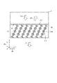
- FIG. 2 is a cross-sectional view schematically showing the structure of the optical element 3. As shown in FIG. It should be noted that the optical waveguide section 1 is indicated by a chain double-dashed line. The optical element 3 shown here corresponds to each of the first layer 3A and the second layer 3B shown in FIG.
- the optical element 3 has a plurality of helical structures 311 .
- Each of the plurality of helical structures 311 extends along the first direction A1. That is, the helical axis AX of each of the multiple helical structures 311 is substantially perpendicular to the second main surface F2 of the optical waveguide section 1 .
- the spiral axis AX is substantially parallel to the first direction A1.
- Each of the multiple helical structures 311 has a helical pitch P. As shown in FIG.
- the spiral pitch P indicates one period (360 degrees) of the spiral.
- Each of the multiple helical structures 311 includes multiple elements 315 .
- the plurality of elements 315 are spirally stacked along the first direction A1 while turning.
- the optical element 3 includes a first boundary surface 317 facing the second main surface F2, a second boundary surface 319 opposite to the first boundary surface 317, and a boundary surface between the first boundary surface 317 and the second boundary surface 319. and a plurality of reflective surfaces 321 of .
- the first boundary surface 317 is a surface on which the light LTi transmitted through the optical waveguide 1 enters the optical element 3 .
- Each of the first boundary surface 317 and the second boundary surface 319 is substantially perpendicular to the spiral axis AX of the spiral structure 311 .
- Each of the first boundary surface 317 and the second boundary surface 319 is substantially parallel to the optical waveguide section 1 (or the second main surface F2).
- the first boundary surface 317 includes an element 315 located at one end e1 of both ends of the helical structure 311 .
- the first boundary surface 317 is located at the boundary between the optical waveguide section 1 and the optical element 3 .
- the second boundary surface 319 includes an element 315 positioned at the other end e2 of the two ends of the spiral structure 311 .
- the second boundary surface 319 is located at the boundary between the optical element 3 and air.
- the multiple reflective surfaces 321 are substantially parallel to each other.
- the reflecting surface 321 is inclined with respect to the first boundary surface 317 and the optical waveguide section 1 (or the second main surface F2), and has a substantially planar shape extending in a certain direction.
- the reflective surface 321 selectively reflects part of the light LTr out of the light LTi incident from the first boundary surface 317 according to Bragg's law. Specifically, the reflecting surface 321 reflects the light LTr such that the wavefront WF of the light LTr is substantially parallel to the reflecting surface 321 . More specifically, the reflecting surface 321 reflects the light LTr according to the inclination angle ⁇ of the reflecting surface 321 with respect to the first boundary surface 317 .
- the reflective surface 321 can be defined as follows. That is, the refractive index felt by light of a predetermined wavelength (for example, circularly polarized light) that is selectively reflected by the optical element 3 changes gradually as the light travels inside the optical element 3 . Therefore, Fresnel reflection gradually occurs in the optical element 3 . Fresnel reflection occurs most strongly at the position where the refractive index sensed by light changes the most in the plurality of helical structures 311 . That is, the reflective surface 321 corresponds to the surface of the optical element 3 where Fresnel reflection occurs most strongly.
- a predetermined wavelength for example, circularly polarized light
- the orientation directions of the elements 315 of the helical structures 311 adjacent to each other in the second direction A2 are different from each other.
- the spatial phases of the spiral structures 311 adjacent to each other in the second direction A2 are different from each other.
- the reflective surface 321 corresponds to a surface in which the orientation directions of the elements 315 are aligned or a surface in which spatial phases are aligned (equiphase surface). That is, each of the multiple reflecting surfaces 321 is inclined with respect to the first boundary surface 317 or the optical waveguide section 1 .
- the shape of the reflecting surface 321 is not limited to the planar shape shown in FIG. Further, a part of the reflecting surface 321 may be uneven, the inclination angle ⁇ of the reflecting surface 321 may not be uniform, or the plurality of reflecting surfaces 321 may not be regularly aligned. Depending on the spatial phase distribution of the plurality of helical structures 311, the reflective surface 321 of any shape can be configured.
- the helical structure 311 is cholesteric liquid crystal.
- Each of the elements 315 corresponds to a liquid crystal molecule.
- one element 315 represents a liquid crystal molecule oriented in the average alignment direction among a plurality of liquid crystal molecules positioned in the XY plane.
- the cholesteric liquid crystal which is the helical structure 311, reflects circularly polarized light in the same turning direction as that of the cholesteric liquid crystal, out of the light of the predetermined wavelength ⁇ included in the selective reflection band ⁇ .
- the rotation direction of the cholesteric liquid crystal is clockwise, the clockwise circularly polarized light of the light with the predetermined wavelength ⁇ is reflected, and the counterclockwise circularly polarized light is transmitted.
- the rotation direction of the cholesteric liquid crystal is counterclockwise, the counterclockwise circularly polarized light of the predetermined wavelength ⁇ is reflected and the clockwise circularly polarized light is transmitted.
- the selective reflection band ⁇ of the cholesteric liquid crystal for vertically incident light is It is indicated by "no*P to ne*P".
- the selective reflection band ⁇ of the cholesteric liquid crystal varies depending on the inclination angle ⁇ of the reflecting surface 321, the angle of incidence on the first boundary surface 317, and the like, with respect to the range of “no*P to ne*P”. Varies accordingly.
- the thickness of the optical element 3 along the first direction A1 is preferably several to ten times the spiral pitch P. That is, the thickness of the optical element 3 is approximately 3 to 10 ⁇ m.
- FIG. 3 is a plan view schematically showing the solar cell device 100.
- FIG. FIG. 3 shows an example of the spatial phase of the helical structure 311. As shown in FIG. The spatial phase shown here is shown as the orientation direction of the elements 315 located on the first boundary surface 317 among the elements 315 included in the helical structure 311 .
- the orientation directions of the elements 315 positioned on the first boundary surface 317 are different for each of the spiral structures 311 arranged along the second direction A2. That is, the spatial phase of the helical structure 311 on the first boundary surface 317 differs along the second direction A2.
- the orientation directions of the elements 315 positioned on the first boundary surface 317 are substantially the same. That is, the spatial phases of the spiral structure 311 on the first boundary surface 317 substantially match in the third direction A3.
- the orientation directions of the respective elements 315 differ by a constant angle. That is, on the first boundary surface 317, the alignment directions of the plurality of elements 315 arranged along the second direction A2 change linearly. Therefore, the spatial phases of the plurality of helical structures 311 arranged along the second direction A2 linearly change along the second direction A2.
- a reflecting surface 321 inclined with respect to the first interface 317 and the optical waveguide section 1 is formed.
- linear change indicates, for example, that the amount of change in the orientation direction of the element 315 is represented by a linear function.
- the alignment direction of the element 315 here corresponds to the major axis direction of the liquid crystal molecules in the XY plane when the helical structure 311 is cholesteric liquid crystal.
- the interval between the two spiral structures 311 when the orientation direction of the element 315 changes by 180 degrees along the second direction A2 is defined as a spiral structure.
- the period T of the body 311 Defines the period T of the body 311 .
- DP in FIG. 3 indicates the turning direction of the element 315 .
- the inclination angle ⁇ of the reflecting surface 321 shown in FIG. 2 is appropriately set according to the period T and the helical pitch P.
- the optical element 3 is formed as follows.
- the optical element 3 is formed by irradiating a plurality of liquid crystal molecules, which are the plurality of elements 315, with light to polymerize the plurality of liquid crystal molecules.
- the optical element 3 by controlling the orientation of a polymer liquid crystal material that exhibits a liquid crystal state at a predetermined temperature or concentration so as to form a plurality of helical structures 311, and then transitioning to a solid state while maintaining the orientation, An optical element 3 is formed.
- the adjacent helical structures 311 are polymerized or transformed into a solid while maintaining the orientation of the helical structures 311, that is, while maintaining the spatial phase of the helical structures 311. Combined.
- the alignment direction of each liquid crystal molecule is fixed in the optical element 3 .
- FIG. 4 is another cross-sectional view schematically showing the structure of the optical element 3.
- the example shown in FIG. 4 differs from the example shown in FIG. 2 in that the helical axis AX of the helical structure 311 is inclined with respect to the optical waveguide section 1 or the second main surface F2.
- the spatial phases of the spiral structure 311 on the first boundary surface 317 or the XY plane are substantially the same.
- the helical structure 311 according to the example shown in FIG. 4 has the same characteristics as the helical structure 311 according to the example shown in FIG.
- the optical element 3 reflects a part of the light LTr out of the light LTi incident through the optical waveguide 1 at a reflection angle corresponding to the inclination of the helical axis AX, and reflects the other light LTt.
- the optical element 3 of the example shown in FIG. 4 also has optical characteristics similar to those of the optical element 3 described with reference to FIGS.
- FIG. 5 is a diagram for explaining the operation of solar cell device 100 shown in FIG. First, the first layer 3A and the second layer 3B of the optical element 3 will be described.
- Each of the first layer 3A and the second layer 3B has unidirectionally swirling cholesteric liquid crystals as the spiral structure 311 .
- the first layer 3A has cholesteric liquid crystals 311A swirled in the first swirling direction
- the second layer 3B has cholesteric liquid crystals 311B swirled in the second swirling direction opposite to the first swirling direction.
- the cholesteric liquid crystals 311A and 311B are shown schematically.
- the cholesteric liquid crystals 311A and 311B both have a helical pitch P1 along the Z direction so as to reflect the infrared rays I as a selective reflection band, as schematically shown in an enlarged manner. That is, the helical pitches P1 of the cholesteric liquid crystal 311A and the cholesteric liquid crystal 311B are the same and are constant along the Z direction with little change.
- the cholesteric liquid crystal 311A has a reflective surface 321A that reflects the first circularly polarized light I1 in the first rotation direction in the infrared rays I that are the selective reflection band.
- the cholesteric liquid crystal 311B has a reflecting surface 321B that reflects the second circularly polarized light I2 in the second turning direction in the infrared rays I, which is the selective reflection band.
- the light LTi that enters the solar cell device 100 is, for example, sunlight. That is, the light LTi includes infrared rays I and the like in addition to the visible light V.
- FIG. Light LTi enters the optical waveguide portion 1 from the first main surface F1, passes through the second main surface F2, and enters the optical element 3. As shown in FIG. Of the light LTi, the optical element 3 reflects a portion of the light LTr toward the optical waveguide section 1 and transmits the other light LTt.
- the first layer 3A and the second layer 3B of the optical element 3 are configured to reflect the infrared rays I. That is, the first circularly polarized light I1 of the infrared rays I is reflected toward the optical waveguide section 1 by the reflecting surface 321A formed on the first layer 3A. The second circularly polarized light I2 of the infrared rays I is reflected toward the optical waveguide section 1 by the reflecting surface 321B formed on the second layer 3B.
- the light LTr reflected by the optical element 3 is the first circularly polarized light I1 and the second circularly polarized light I2 of the infrared light I.
- the light LTt transmitted through the optical element 3 has a wavelength different from that of the infrared rays I, and includes visible light V. As shown in FIG.
- the optical element 3 reflects the first circularly polarized light I1 and the second circularly polarized light I2 toward the optical waveguide section 1 at an incident angle ⁇ that satisfies the optical waveguide condition in the optical waveguide section 1 .
- the incident angle ⁇ here corresponds to an angle equal to or greater than the critical angle ⁇ c that causes total reflection inside the optical waveguide 1 .
- the incident angle ⁇ indicates an angle with respect to a perpendicular line perpendicular to the optical waveguide section 1 .
- the light LTr enters the inside of the optical waveguide portion 1 from the second main surface F2 and propagates inside the optical waveguide portion 1 while being repeatedly reflected in the optical waveguide portion 1 . Most of the light LTr propagating inside the optical waveguide 1 is transmitted through the side surface F3.
- the first photoelectric conversion element 51 receives the light LTr (the first circularly polarized light I1 and the second circularly polarized light I2 of the infrared rays I) transmitted through the side surface F3 and generates power.
- the light LTr contains s-polarized light and p-polarized light.
- the s-polarized light is totally reflected by the first main surface F1 and the second main surface F2, but the p-polarized light is transmitted through the first main surface F1 and the second main surface F2, respectively.
- the second photoelectric conversion element (first element) 52A receives light LTr (p-polarized light of infrared rays I) transmitted through the first main surface F1 and generates power.
- the second photoelectric conversion element (second element) 52B receives light LTr (p-polarized light of infrared rays I) transmitted through the second main surface F2 and generates power.
- the solar cell device 100 of Embodiment 1 not only the light transmitted through the side surface F3 of the optical waveguide 1 but also the light leaked from the first main surface F1 and the second main surface F2 can be used for power generation. can be used. Therefore, light utilization efficiency can be improved.
- the optical element 3 has the first layer 3A and the second layer 3B
- when sunlight containing visible light V and infrared light I is incident on the solar cell device 100 the first circularly polarized light I1 of the infrared light I and The second circularly polarized light I2 can be used for power generation in the first photoelectric conversion element 51 and the second photoelectric conversion elements 52A and 52B.
- visible light V in sunlight passes through the optical waveguide 1 and the optical element 3 . That is, the solar cell device 100 transmits each of the first component (blue component), the second component (green component), and the third component (red component), which are the main components of the visible light V. FIG. Therefore, coloring of the light transmitted through the solar cell device 100 can be suppressed. Moreover, it is possible to suppress a decrease in the transmittance of the visible light V in the solar cell device 100 .
- the second photoelectric conversion elements 52A and 52B which are coating-type organic semiconductor solar cells, are extremely thin and can be formed in any region at low cost.
- FIG. 6 is a cross-sectional view schematically showing a solar cell device 100 according to Embodiment 2.
- FIG. Embodiment 2 shown in FIG. 6 differs from Embodiment 1 above in that a wavelength conversion layer 60 is provided instead of the second photoelectric conversion element.
- the wavelength conversion layer 60 faces at least one of the first main surface F1 and the second main surface F2.
- the wavelength conversion layer 60 faces both the first main surface F1 and the second main surface F2.
- the wavelength conversion layer 60 facing the first main surface F1 in the first direction A1 is referred to as a first conversion layer 60A
- the wavelength conversion layer 60 facing the second main surface F2 in the first direction A1 is referred to as a second conversion layer 60A.
- layer 60B for distinction.
- the first conversion layer 60A and the second conversion layer 60B are made of substantially the same material.
- the wavelength conversion layer 60 only one of the first conversion layer 60A and the second conversion layer 60B may be arranged.
- the wavelength conversion layer 60 converts visible light, which is incident light, into infrared light, but may also convert ultraviolet light into visible light or infrared light, or convert infrared light into visible light.
- the wavelength band of light after conversion by the wavelength conversion layer 60 is selected to correspond to the sensitivity of the first photoelectric conversion element 51 .
- Such a wavelength conversion layer 60 is formed, for example, by applying an inorganic fluorescent material or an organic fluorescent material.
- the wavelength conversion layer 60 the light converted to a predetermined wavelength tends to scatter. Therefore, from the viewpoint of efficiently reflecting the light toward the optical waveguide section 1, the wavelength conversion layer 60 should be covered with a reflective layer. is desirable.
- the frame 40 surrounds the first photoelectric conversion element 51 and the wavelength conversion layer 60 .
- the first photoelectric conversion element 51 is positioned between the side surface F3 of the optical waveguide section 1 and the frame 40 .
- the first conversion layer 60A of the wavelength conversion layer 60 is positioned between the first main surface F1 of the optical waveguide 1 and the frame 40, and the second conversion layer 60B is positioned between the second main surface F2 and the frame 40. is doing.
- infrared rays I of the sunlight pass through the optical waveguide 1 and enter the optical element 3 .
- the first circularly polarized light I1 of the infrared rays I is reflected toward the optical waveguide section 1 by the reflecting surface 321A formed on the first layer 3A.
- the second circularly polarized light I2 of the infrared rays I is incident on the second layer 3B after passing through the first layer 3A, and is directed toward the optical waveguide section 1 on the reflecting surface 321B formed on the second layer 3B. reflected.
- the reflected first circularly polarized light I1 and second circularly polarized light I2 enter the optical waveguide section 1 from the second main surface F2 and propagate through the optical waveguide section 1 while being repeatedly reflected in the optical waveguide section 1. .
- Most of the light LTr propagating inside the optical waveguide 1 is transmitted through the side surface F3.
- the first photoelectric conversion element 51 receives the infrared rays I (the first circularly polarized light I1 and the second circularly polarized light I2) transmitted through the side surface F3 and generates electric power.
- a part of the visible light V′ that is incident at the incident angle ⁇ that satisfies the above optical waveguide condition propagates inside the optical waveguide 1 while being repeatedly reflected in the optical waveguide 1 .
- Visible light V' leaking from the first main surface F1 near the side surface F3 is converted into infrared rays I in the first conversion layer 60A.
- Visible light V' leaked from the second main surface F2 near the side surface F3 is converted into infrared rays I in the second conversion layer 60B.
- the infrared rays I converted by the first conversion layer 60A and the second conversion layer 60B pass through the optical waveguide portion 1 again and pass through the side surface F3.
- the first photoelectric conversion element 51 receives the infrared rays I transmitted through the side surface F3 and generates electric power.
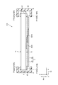
- the visible light V' leaked from the first main surface F1 and the second main surface F2 is converted into light with a wavelength that can be used for power generation, and is used for power generation. Therefore, light utilization efficiency can be improved.
- FIG. 7 is a plan view showing the appearance of the solar cell device 100.
- FIG. A frame 40 indicated by a dotted line is arranged so as to surround the optical waveguide section 1 .
- the plurality of first photoelectric conversion elements 51 are arranged along the side surface F3 of the optical waveguide section 1 .
- the second photoelectric conversion element 52 of Embodiment 1 or the wavelength conversion layer 60 of Embodiment 2 is formed in a belt shape along at least the side surface F3.
- the second photoelectric conversion element 52 or the wavelength conversion layer 60 is formed in a frame shape on at least one of the first main surface F1 and the second main surface F2 of the optical waveguide section 1, and is attached to the frame 40. are superimposed.
- the second photoelectric conversion element 52 or the wavelength conversion layer 60 has portions P11 to P14 along the four sides of the optical waveguide section 1 .
- the parts P11 to P14 may be connected to each other or may be separated from each other.
- at least part of the portions P12 to P14 may be omitted.
- each of the portions P11 to P14 may protrude from the frame 40.
- FIG. 8 is a cross-sectional view of the solar cell device 100 shown in FIG. 7 along line AB.
- the portions P11 and P13 are formed on both the first main surface F1 and the second main surface F2.
- Portions P12 and P14 (not shown) are similarly formed on both the first main surface F1 and the second main surface F2.
- the portions P11 and P13 formed on the first main surface F1 are part of the first element (second photoelectric conversion element) 52A or part of the first conversion layer (wavelength conversion layer) 60A.
- the portions P11 and P13 formed on the second main surface F2 are part of the second element (second photoelectric conversion element) 52B or part of the second conversion layer (wavelength conversion layer) 60B.
- the first layer 3A and the second layer 3B of the optical element 3 are arranged inside the second main surface F2 surrounded by the second element 52B or the second conversion layer 60B.
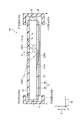
- FIG. 9 is another cross-sectional view of the solar cell device 100 shown in FIG. 7 along line AB.
- the example shown in FIG. 9 differs from the example shown in FIG. 8 in that a transparent thin film 70 facing the first main surface F1 is provided.
- the thin film 70 is arranged inside the frame 40, is in contact with the first main surface F1, and is arranged inside the first element 52A or the first conversion layer 60A.
- the refractive index of the thin film 70 is smaller than that of the optical waveguide section 1 . It is desirable that the difference in refractive index between the thin film 70 and the optical waveguide section 1 is 0.1 or more.
- the thin film 70 has a refractive index of about 1.3 to 1.4, and the optical waveguide section 1 has a refractive index of about 1.5.
- Such a thin film 70 may be made of an inorganic material, or may be made of an organic material.
- a thin film 70 having a refractive index lower than that of the optical waveguide section 1 is arranged on the first main surface F1.
- the refractive index difference between the thin film 70 and the air becomes smaller than the refractive index difference between the optical waveguide 1 and the air.
- the reflected light beams LTr(I1) and LTr(I2) with a smaller reflection angle ⁇ r from the light beam can be optically guided and used for power generation. Therefore, light utilization efficiency can be improved.
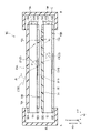
- FIG. 10 is another cross-sectional view along the line AB of the solar cell device 100 shown in FIG.
- the example shown in FIG. 10 differs from the example shown in FIG. 9 in that the solar cell device 100 includes a plurality of optical waveguides 1A and 1B facing each other in the first direction A1.
- the optical waveguides 1A and 1B are equivalent to the optical waveguide 1 described above.
- Thin films 70A and 70B are equivalent to thin film 70 described above.
- the refractive index of the thin film 70A is smaller than that of the optical waveguide 1A, and the refractive index of the thin film 70B is smaller than that of the optical waveguide 1B.
- the first photoelectric conversion elements 51A and 51B are equivalent to the first photoelectric conversion element 51 described above.
- the second photoelectric conversion elements 52A, 52B, 52C, and 52D are equivalent to the second photoelectric conversion element 52 described above.
- the optical waveguide section 1A has a first main surface F1A, a second main surface F2A, and a side surface F3A.
- the thin film 70A is arranged on the first main surface F1A
- the first layer 3A is arranged on the second main surface F2A
- the first photoelectric conversion element 51A is arranged on the side surface F3A.
- the second photoelectric conversion element 52A is arranged on the first main surface F1A
- the second photoelectric conversion element 52B is arranged on the second main surface F2A.
- a frame 40 surrounds the first photoelectric conversion element 51A and the second photoelectric conversion elements 52A and 52B.
- the optical waveguide section 1B has a first main surface F1B, a second main surface F2B, and a side surface F3B.
- the thin film 70B is arranged on the first main surface F1B
- the second layer 3B is arranged on the second main surface F2B
- the first photoelectric conversion element 51B is arranged on the side surface F3B.
- the second photoelectric conversion element 52C is arranged on the first main surface F1B
- the second photoelectric conversion element 52D is arranged on the second main surface F2B.
- the first photoelectric conversion element 51B and the second photoelectric conversion elements 52C and 52D are surrounded by a frame 40. As shown in FIG.
- the first layer 3A and the thin film 70B face each other in the first direction A1.
- An intermediate layer such as an air layer is interposed between the first layer 3A and the thin film 70B.
- An infrared ray I having an incident angle ⁇ i passes through the thin film 70A and the optical waveguide 1A and enters the first layer 3A.
- the provision of the thin film 70A allows even the infrared rays I with a relatively large incident angle .theta.i to be taken into the optical waveguide portion 1A.
- the first circularly polarized light I1 of the infrared rays I is reflected toward the optical waveguide section 1A on the reflecting surface 321A formed on the first layer 3A.
- the second circularly polarized light I2 of the infrared rays I passes through the thin film 70B and the optical waveguide portion 1B after passing through the first layer 3A, and enters the second layer 3B. Then, the second circularly polarized light I2 is reflected toward the optical waveguide portion 1B by the reflecting surface 321B formed on the second layer 3B.
- the first circularly polarized light I1 reflected toward the optical waveguide portion 1A propagates while being repeatedly reflected in the optical waveguide portion 1A, and most of it is transmitted through the side surface F3A.
- the first photoelectric conversion element 51A receives the first circularly polarized light I1 transmitted through the side surface F3A and generates power.
- the second photoelectric conversion element 52A receives the p-polarized light transmitted through the first main surface F1A in the vicinity of the side surface F3A and generates electric power.
- the second photoelectric conversion element 52B receives the p-polarized light transmitted through the second main surface F2A in the vicinity of the side surface F3A and generates electric power.
- the second circularly polarized light I2 reflected toward the optical waveguide portion 1B propagates while being repeatedly reflected in the optical waveguide portion 1B, and most of it is transmitted through the side surface F3B.
- the first photoelectric conversion element 51B receives the second circularly polarized light I2 transmitted through the side face F3B and generates power.
- the second photoelectric conversion element 52C receives the p-polarized light transmitted through the first main surface F1B in the vicinity of the side surface F3B and generates electric power.
- the second photoelectric conversion element 52D receives the p-polarized light transmitted through the second main surface F2B in the vicinity of the side surface F3B and generates electric power.
- the second photoelectric conversion elements 52A, 52B, 52C, and 52D shown in FIG. 10 may be replaced with the wavelength conversion layer 60 described in the second embodiment.
Landscapes
- Physics & Mathematics (AREA)
- Electromagnetism (AREA)
- General Physics & Mathematics (AREA)
- Optics & Photonics (AREA)
- Photovoltaic Devices (AREA)
- Optical Filters (AREA)
- Optical Elements Other Than Lenses (AREA)
Abstract
実施形態の目的は、光の利用効率を向上することが可能な太陽電池装置を提供することにある。 一実施形態によれば、太陽電池装置(100)は、第1主面(F1)と、前記第1主面(F1)と対向する第2主面(F2)と、側面(F3)と、を有する光導波部(1)と、前記第2主面(F2)と対向し、コレステリック液晶を有し、前記光導波部(1)を介して入射した光の少なくとも一部を前記光導波部(1)に向けて反射する光学素子(3)と、前記側面(F3)と対向する第1光電変換素子(51)と、前記第1主面(F1)及び前記第2主面(F2)の少なくとも一方と対向し、前記側面(F3)に沿った帯状に形成された第2光電変換素子(52)と、を備え、前記第1光電変換素子(51)の厚さは、前記第2光電変換素子(52)の厚さより厚い。
Description
本発明の実施形態は、太陽電池装置に関する。
近年、透明な太陽電池が種々提案されている。例えば、透明な色素増感型太陽電池を表示装置の表面に配置した太陽電池付き表示装置が提案されている。
太陽電池装置において、光の利用効率を向上することが要望されている。
太陽電池装置において、光の利用効率を向上することが要望されている。
本実施形態の目的は、光の利用効率を向上することが可能な太陽電池装置を提供することにある。
一実施形態の太陽電池装置は、
第1主面と、前記第1主面と対向する第2主面と、側面と、を有する光導波部と、前記第2主面と対向し、コレステリック液晶を有し、前記光導波部を介して入射した光の少なくとも一部を前記光導波部に向けて反射する光学素子と、前記側面と対向する第1光電変換素子と、前記第1主面及び前記第2主面の少なくとも一方と対向し、前記側面に沿った帯状に形成された第2光電変換素子と、を備え、前記第1光電変換素子の厚さは、前記第2光電変換素子の厚さより厚い。
一実施形態の太陽電池装置は、
第1主面と、前記第1主面と対向する第2主面と、側面と、を有する光導波部と、前記第2主面と対向し、コレステリック液晶を有し、前記光導波部を介して入射した光の少なくとも一部を前記光導波部に向けて反射する光学素子と、前記側面と対向する第1光電変換素子と、前記第1主面及び前記第2主面の少なくとも一方に対向し、前記側面に沿った帯状に形成された波長変換層と、を備えている。
第1主面と、前記第1主面と対向する第2主面と、側面と、を有する光導波部と、前記第2主面と対向し、コレステリック液晶を有し、前記光導波部を介して入射した光の少なくとも一部を前記光導波部に向けて反射する光学素子と、前記側面と対向する第1光電変換素子と、前記第1主面及び前記第2主面の少なくとも一方と対向し、前記側面に沿った帯状に形成された第2光電変換素子と、を備え、前記第1光電変換素子の厚さは、前記第2光電変換素子の厚さより厚い。
一実施形態の太陽電池装置は、
第1主面と、前記第1主面と対向する第2主面と、側面と、を有する光導波部と、前記第2主面と対向し、コレステリック液晶を有し、前記光導波部を介して入射した光の少なくとも一部を前記光導波部に向けて反射する光学素子と、前記側面と対向する第1光電変換素子と、前記第1主面及び前記第2主面の少なくとも一方に対向し、前記側面に沿った帯状に形成された波長変換層と、を備えている。
一実施形態によれば、光の利用効率を向上することが可能な太陽電池装置を提供することができる。
以下、本実施形態について、図面を参照しながら説明する。なお、開示はあくまで一例に過ぎず、当業者において、発明の主旨を保っての適宜変更について容易に想到し得るものについては、当然に本発明の範囲に含有されるものである。また、図面は、説明をより明確にするため、実際の態様に比べて、各部の幅、厚さ、形状等について模式的に表される場合があるが、あくまで一例であって、本発明の解釈を限定するものではない。また、本明細書と各図において、既出の図に関して前述したものと同一又は類似した機能を発揮する構成要素には同一の参照符号を付し、重複する詳細な説明を適宜省略することがある。
なお、図面には、必要に応じて理解を容易にするために、互いに直交するX軸、Y軸、及び、Z軸を記載する。Z軸に沿った方向をZ方向または第1方向A1と称し、Y軸に沿った方向をY方向または第2方向A2と称し、X軸に沿った方向をX方向または第3方向A3と称する。X軸及びY軸によって規定される面をX-Y平面と称し、X軸及びZ軸によって規定される面をX-Z平面と称し、Y軸及びZ軸によって規定される面をY-Z平面と称する。
(実施形態1)
図1は、実施形態1に係る太陽電池装置100を模式的に示す断面図である。
太陽電池装置100は、光導波部1と、光学素子3と、第1光電変換素子51と、第2光電変換素子52と、を備えている。
図1は、実施形態1に係る太陽電池装置100を模式的に示す断面図である。
太陽電池装置100は、光導波部1と、光学素子3と、第1光電変換素子51と、第2光電変換素子52と、を備えている。
光導波部1は、光を透過する透明部材、例えば、透明なガラス板または透明な合成樹脂板によって構成されている。光導波部1は、例えば、可撓性を有する透明な合成樹脂板によって構成されていてもよい。光導波部1は、任意の形状を取り得る。例えば、光導波部1は、湾曲していてもよい。光導波部1の屈折率は、例えば、空気の屈折率よりも大きい。光導波部1は、例えば、窓ガラスとして機能する。
本明細書において、『光』は、可視光及び不可視光を含むものである。例えば、可視光域の下限の波長は360nm以上400nm以下であり、可視光域の上限の波長は760nm以上830nm以下である。可視光は、第1波長帯(例えば400nm~500nm)の第1成分(青成分)、第2波長帯(例えば500nm~600nm)の第2成分(緑成分)、及び、第3波長帯(例えば600nm~700nm)の第3成分(赤成分)を含んでいる。不可視光は、第1波長帯より短波長帯の紫外線、及び、第3波長帯より長波長帯の赤外線を含んでいる。
本明細書において、『透明』は、無色透明であることが好ましい。ただし、『透明』は、半透明又は有色透明であってもよい。
本明細書において、『透明』は、無色透明であることが好ましい。ただし、『透明』は、半透明又は有色透明であってもよい。
光導波部1は、X-Y平面に沿った平板状に形成され、第1主面F1と、第2主面F2と、側面F3と、を有している。第1主面F1及び第2主面F2は、X-Y平面に略平行な面であり、第1方向A1において、互いに対向している。側面F3は、第1方向A1に沿って延びた面である。図1に示す例では、側面F3は、X-Z平面と略平行な面であるが、側面F3は、Y-Z平面と略平行な面を含んでいる。
光導波部1が窓ガラスとして機能する場合、第1主面F1は屋外側(あるいは車外側)の面に相当し、第2主面F2は屋内側(あるいは車内側)の面に相当する。
光導波部1が窓ガラスとして機能する場合、第1主面F1は屋外側(あるいは車外側)の面に相当し、第2主面F2は屋内側(あるいは車内側)の面に相当する。
光学素子3は、第1方向A1において、光導波部1の第2主面F2と対向している。光学素子3は、第1主面F1の側から入射した光の少なくとも一部を光導波部1に向けて反射するものである。一例では、光学素子3は、光導波部1を介して入射した光のうち、第1円偏光及び第1円偏光とは逆回りの第2円偏光の少なくとも一方を反射するように構成されている。光学素子3によって反射される第1円偏光及び第2円偏光は、例えば赤外線であるが、可視光であってもよい。なお、本明細書において、光学素子3における「反射」とは、光学素子3の内部における回折を伴うものである。
光学素子3は、例えば、可撓性を有していてもよい。また、光学素子3は、光導波部1の第2主面F2と接触していてもよいし、光学素子3と光導波部1との間に接着層等の透明な層が介在していてもよい。光学素子3と光導波部1との間に介在する層の屈折率は、光導波部1の屈折率とほぼ同等であることが好ましい。
光学素子3は、薄膜として構成される。例えば、別途フィルム状に形成された光学素子3が光導波部1に接着される場合もあり得るし、光導波部1に直接材料を塗布してフィルム状の光学素子3が形成される場合もあり得る。
図1に示す例では、光学素子3は、第1層3Aと、第2層3Bと、を備えている。第1層3A及び第2層3Bは、第1方向A1において重なっている。第1層3Aは、光導波部1と第2層3Bとの間に位置している。光学素子3の各層については、後に詳述するが、例えば、第1層3Aは第1円偏光を反射するように構成され、第2層3Bは第2円偏光を反射するように構成されている。なお、光学素子3は、第1層3Aからなる単層体、あるいは、第2層3Bからなる単層体であってもよい。本明細書において、円偏光は、厳密な円偏光であってもよいし、楕円偏光に近似した円偏光であってもよい。
第1光電変換素子51は、第2方向A2において、光導波部1の側面F3と対向している。
第2光電変換素子52は、第1主面F1及び第2主面F2の少なくとも一方と対向している。図1に示す例では、第2光電変換素子52は、第1主面F1及び第2主面F2の双方と対向している。ここでは、第1方向A1において第1主面F1に対向する第2光電変換素子52を第1素子52Aと称し、第1方向A1において第2主面F2に対向する第2光電変換素子52を第2素子52Bと称して、区別する場合がある。第1素子52A及び第2素子52Bは、実質的に同一構造を有するものである。なお、第2光電変換素子52としては、第1素子52A及び第2素子52Bのいずれか一方のみが配置されていてもよい。
第2光電変換素子52は、第1主面F1及び第2主面F2の少なくとも一方と対向している。図1に示す例では、第2光電変換素子52は、第1主面F1及び第2主面F2の双方と対向している。ここでは、第1方向A1において第1主面F1に対向する第2光電変換素子52を第1素子52Aと称し、第1方向A1において第2主面F2に対向する第2光電変換素子52を第2素子52Bと称して、区別する場合がある。第1素子52A及び第2素子52Bは、実質的に同一構造を有するものである。なお、第2光電変換素子52としては、第1素子52A及び第2素子52Bのいずれか一方のみが配置されていてもよい。
フレーム40は、第1光電変換素子51及び第2光電変換素子52を囲んでいる。第1光電変換素子51は、光導波部1の側面F3とフレーム40との間に位置している。第2光電変換素子52について、第1素子52Aは光導波部1の第1主面F1とフレーム40との間に位置し、第2素子52Bは第2主面F2とフレーム40との間に位置している。
第1光電変換素子51及び第2光電変換素子52は、光を受光して、受光した光のエネルギーを電力に変換するものであり、太陽電池と称する場合がある。つまり、太陽電池は、受光した光によって発電するものであるが、第1光電変換素子51及び第2光電変換素子52として適用される太陽電池の種類は、特に限定されない。例えば、太陽電池は、シリコン系太陽電池、化合物半導体系太陽電池、有機半導体系太陽電池、ペロブスカイト型太陽電池、又は、量子ドット型太陽電池である。
一例では、第1光電変換素子51及び第2光電変換素子52は、赤外線を受光して発電するように構成されている。
一例では、第1光電変換素子51及び第2光電変換素子52は、赤外線を受光して発電するように構成されている。
第1光電変換素子51は、例えば、シリコン系太陽電池、あるいは、化合物半導体系太陽電池である。図1の右側に拡大して示すように、第1光電変換素子51は、透明電極E11と、pin層A10と、金属電極E12と、を備えている。透明電極E11は、第2方向A2において側面F3と対向している。pin層A10は、透明電極E11と金属電極E12との間に位置している。このような第1光電変換素子51は、封止体S51によって封止されている。
pin層A10は、シリコン系半導体、あるいは、無機化合物系半導体によって形成されている。図1に示す例では、pin層A10は、ヘテロ接合型であり、n型半導体層(n層)A11、n型/p型半導体の界面に形成される空乏層(i層)A12、及び、p型半導体層(p層)A13の積層体として構成されている。pin層A10の厚さT1は、n層A11の膜厚、i層A12の膜厚、及び、p層A13の膜厚の総和に相当する。一例では、厚さT1は、1μm以上である。
第2光電変換素子52は、塗布型の有機半導体系太陽電池である。図1の上側に拡大して示すように、第2光電変換素子52は、透明電極E21と、バッファ層B21と、活性層A20と、バッファ層B22と、金属電極E22と、を備えている。透明電極E21は、第1方向A1において第1主面F1と対向している。なお、透明電極E21は、第1主面F1に接していてもよいし、第1主面F1と透明電極E21との間に他の薄膜が介在していてもよい。活性層A20は、透明電極E21と金属電極E22との間に位置している。バッファ層B21は、透明電極E21と活性層A20との間に位置している。バッファ層B22は、活性層A20と金属電極E22との間に位置している。このような第2光電変換素子52は、封止体S52によって封止されている。
活性層A20は、有機半導体によって形成されている。図1に示す例では、活性層A20は、バルクヘテロ接合型であり、電子受容体及び電子供与体を含む混合層として構成されている。活性層A20の厚さT2は、バッファ層B21とバッファ層B22との間において、一例では、100~500nmである。つまり、pin層A10の厚さT1>活性層A20の厚さT2の関係から、第1光電変換素子51の厚さは、第2光電変換素子52の厚さより大きい。
このような第2光電変換素子52を構成する各層は、例えば材料を塗布することによって形成されるが、蒸着やスパッタリングなどの真空プロセスで形成してもよいし、前駆体やナノ粒子からなる溶液を塗布した後に焼成することで形成してもよい。
以下に、各部材の材料の一例について説明する。なお、一部の有機化合物については略称で示す場合がある。
透明電極E11及びE21は、例えば、インジウム錫酸化物(ITO)、インジウム亜鉛酸化物(IZO)などの透明な導電材料によって形成される。
金属電極E12及びE22は、例えば、銀(Ag)、アルミニウム(Al)などの金属材料によって形成される。
金属電極E12及びE22は、例えば、銀(Ag)、アルミニウム(Al)などの金属材料によって形成される。
バッファ層B21及びB22のいずれか一方はホール輸送層(HTL)として機能するものであり、バッファ層B21及びB22のいずれか他方は電子輸送層(ETL)として機能するものである。ホール輸送層は、例えば、PEDOT:PSSなどの有機半導体ポリマーや、モリブデン酸化物(MoO3)、タングステン酸化物(WO3)、バナジウム酸化物(V2O5)、ニッケル酸化物(NiO)などの金属酸化物によって形成される。電子輸送層は、亜鉛酸化物(ZnO)、チタン酸化物(TiO)などの金属酸化物や、PEIE、PEIなどの有機ポリマー化合物によって形成される。
活性層A20を構成する電子受容体は、PTT、PDDTT、PDTTP、P4、PTZBTTT-BDT、PCPDTBT、PDT、PDPP3T、PBTI(EDOT)、PMDPP3T、LBPP-1などのp型有機半導体によって形成される。
活性層A20を構成する電子供与体は、[60]PCBM、[70]PCBMなどのn型有機半導体によって形成される。
活性層A20を構成する電子供与体は、[60]PCBM、[70]PCBMなどのn型有機半導体によって形成される。
図2は、光学素子3の構造を模式的に示す断面図である。
なお、光導波部1は二点鎖線で示している。ここに示す光学素子3は、図1に示した第1層3A及び第2層3Bのそれぞれに相当するものである。
なお、光導波部1は二点鎖線で示している。ここに示す光学素子3は、図1に示した第1層3A及び第2層3Bのそれぞれに相当するものである。
光学素子3は、複数の螺旋状構造体311を有している。複数の螺旋状構造体311の各々は、第1方向A1に沿って延びている。つまり、複数の螺旋状構造体311の各々の螺旋軸AXは、光導波部1の第2主面F2に対して略垂直である。螺旋軸AXは、第1方向A1に略平行である。複数の螺旋状構造体311の各々は、螺旋ピッチPを有している。螺旋ピッチPは、螺旋の1周期(360度)を示す。複数の螺旋状構造体311の各々は、複数の要素315を含んでいる。複数の要素315は、旋回しながら第1方向A1に沿って螺旋状に積み重ねられている。
光学素子3は、第2主面F2に対向する第1境界面317と、第1境界面317の反対側の第2境界面319と、第1境界面317と第2境界面319との間の複数の反射面321と、を有している。第1境界面317は、光導波部1を透過した光LTiが光学素子3に入射する面である。第1境界面317及び第2境界面319の各々は、螺旋状構造体311の螺旋軸AXに対して略垂直である。第1境界面317及び第2境界面319の各々は、光導波部1(あるいは第2主面F2)に略平行である。
第1境界面317は、螺旋状構造体311の両端部のうちの一端部e1に位置する要素315を含んでいる。第1境界面317は、光導波部1と光学素子3との境界に位置している。第2境界面319は、螺旋状構造体311の両端部のうちの他端部e2に位置する要素315を含んでいる。第2境界面319は、光学素子3と空気との境界に位置している。
図2に示す例では、複数の反射面321は、互いに略平行である。反射面321は、第1境界面317及び光導波部1(あるいは第2主面F2)に対して傾斜しており、一定方向に延びる略平面形状を有している。反射面321は、ブラッグの法則に従って、第1境界面317から入射した光LTiのうち一部の光LTrを選択反射する。具体的には、反射面321は、光LTrの波面WFが反射面321と略平行になるように、光LTrを反射する。更に具体的には、反射面321は、第1境界面317に対する反射面321の傾斜角度φに応じて光LTrを反射する。
反射面321は、次のように定義できる。すなわち、光学素子3において選択的に反射される所定波長の光(例えば円偏光)が感じる屈折率は、光が光学素子3の内部を進行するのに伴って徐々に変化する。このため、光学素子3においてフレネル反射が徐々に起こる。そして、複数の螺旋状構造体311において光が感じる屈折率が最も大きく変化する位置で、フレネル反射が最も強く起こる。つまり、反射面321は、光学素子3においてフレネル反射が最も強く起こる面に相当する。
複数の螺旋状構造体311のうち、第2方向A2に隣接する螺旋状構造体311の各々の要素315の配向方向は互いに異なっている。また、複数の螺旋状構造体311のうち、第2方向A2に隣接する螺旋状構造体311の各々の空間位相は互いに異なっている。反射面321は、要素315の配向方向が揃った面、あるいは、空間位相が揃った面(等位相面)に相当する。つまり、複数の反射面321の各々は、第1境界面317あるいは光導波部1に対して傾斜している。
なお、反射面321の形状は、図2に示したような平面形状に限らず、凹状や凸状の曲面形状であってもよく、特に限定されるものではない。また、反射面321の一部に凸凹を有していたり、反射面321の傾斜角度φが均一でなかったり、複数の反射面321が、規則的に整列していなかったりしてもよい。複数の螺旋状構造体311の空間位相分布に応じて、任意の形状の反射面321を構成することができる。
本実施形態では、螺旋状構造体311は、コレステリック液晶である。要素315の各々は、液晶分子に相当する。図2では、図面の簡略化のため、1つの要素315は、X-Y平面内に位置する複数の液晶分子のうち、平均的配向方向を向いている液晶分子を代表して示している。
螺旋状構造体311であるコレステリック液晶は、選択反射帯域Δλに含まれる所定波長λの光のうち、コレステリック液晶の旋回方向と同じ旋回方向の円偏光を反射する。例えば、コレステリック液晶の旋回方向が右回りの場合、所定波長λの光のうち、右回りの円偏光を反射し、左回りの円偏光を透過する。同様に、コレステリック液晶の旋回方向が左回りの場合、所定波長λの光のうち、左回りの円偏光を反射し、右回りの円偏光を透過する。
コレステリック液晶の螺旋ピッチをP、液晶分子の異常光に対する屈折率をne、液晶分子の常光に対する屈折率をnoと記載すると、一般的に、垂直入射した光に対するコレステリック液晶の選択反射帯域Δλは、「no*P~ne*P」で示される。なお、詳細には、コレステリック液晶の選択反射帯域Δλは、「no*P~ne*P」の範囲に対して、反射面321の傾斜角度φや、第1境界面317への入射角度などに応じて変化する。
ここでは、選択反射帯域Δλが赤外線となるように、コレステリック液晶の螺旋ピッチPが調整された場合について説明する。光学素子3の反射面321での反射率を高くする観点では、光学素子3の第1方向A1に沿った厚さは、螺旋ピッチPの数倍から10倍程度とすることが望ましい。つまり、光学素子3の厚さは、3~10μm程度となる。
図3は、太陽電池装置100を模式的に示す平面図である。
図3には、螺旋状構造体311の空間位相の一例が示されている。ここに示す空間位相は、螺旋状構造体311に含まれる要素315のうち、第1境界面317に位置する要素315の配向方向として示している。
図3には、螺旋状構造体311の空間位相の一例が示されている。ここに示す空間位相は、螺旋状構造体311に含まれる要素315のうち、第1境界面317に位置する要素315の配向方向として示している。
第2方向A2に沿って並んだ螺旋状構造体311の各々について、第1境界面317に位置する要素315の配向方向は互いに異なる。つまり、第1境界面317における螺旋状構造体311の空間位相は、第2方向A2に沿って異なる。
一方、第3方向A3に沿って並んだ螺旋状構造体311の各々について、第1境界面317に位置する要素315の配向方向は略一致する。つまり、第1境界面317における螺旋状構造体311の空間位相は、第3方向A3において略一致する。
一方、第3方向A3に沿って並んだ螺旋状構造体311の各々について、第1境界面317に位置する要素315の配向方向は略一致する。つまり、第1境界面317における螺旋状構造体311の空間位相は、第3方向A3において略一致する。
特に、第2方向A2に並んだ螺旋状構造体311に着目すると、各要素315の配向方向は、一定角度ずつ異なっている。つまり、第1境界面317において、第2方向A2に沿って並んだ複数の要素315の配向方向は、線形に変化している。したがって、第2方向A2に沿って並んだ複数の螺旋状構造体311の空間位相は、第2方向A2に沿って線形に変化している。その結果、図2に示した光学素子3のように、第1境界面317及び光導波部1に対して傾斜する反射面321が形成される。ここでの「線形に変化」は、例えば、要素315の配向方向の変化量が1次関数で表されることを示す。
なお、ここでの要素315の配向方向とは、螺旋状構造体311がコレステリック液晶の場合、X-Y平面における液晶分子の長軸方向に相当する。
ここで、図3に示すように、第1境界面317において、第2方向A2に沿って要素315の配向方向が180度だけ変化するときの2つの螺旋状構造体311の間隔を螺旋状構造体311の周期Tと定義する。なお、図3においてDPは要素315の旋回方向を示している。図2に示した反射面321の傾斜角度φは、周期T及び螺旋ピッチPによって適宜設定される。
螺旋状構造体311がコレステリック液晶である場合、光学素子3は、以下のようにして形成される。例えば、複数の要素315である複数の液晶分子に光を照射し、複数の液晶分子を重合させることで、光学素子3が形成される。又は、所定の温度又は所定の濃度において液晶状態を示す高分子液晶材料を、複数の螺旋状構造体311を形成するように配向制御し、その後、配向を維持したまま固体に転移させることで、光学素子3が形成される。
光学素子3において、隣り合う螺旋状構造体311は、重合又は固体への転移によって、螺旋状構造体311の配向を維持したまま、つまり、螺旋状構造体311の空間位相を維持したまま、互いに結合している。その結果、光学素子3において、各液晶分子の配向方向が固定されている。
光学素子3において、隣り合う螺旋状構造体311は、重合又は固体への転移によって、螺旋状構造体311の配向を維持したまま、つまり、螺旋状構造体311の空間位相を維持したまま、互いに結合している。その結果、光学素子3において、各液晶分子の配向方向が固定されている。
図4は、光学素子3の構造を模式的に示す他の断面図である。
図4に示す例は、図2に示した例と比較して、螺旋状構造体311の螺旋軸AXが光導波部1あるいは第2主面F2に対して傾斜している点で相違している。また、図4に示す例では、第1境界面317あるいはX-Y平面内での螺旋状構造体311の空間位相は、略一致している。その他、図4に示す例に係る螺旋状構造体311は、図2に示した例に係る螺旋状構造体311と同様の特性を有している。
このような例では、光学素子3は、光導波部1を介して入射した光LTiのうち、一部の光LTrを螺旋軸AXの傾斜に応じた反射角で反射し、その他の光LTtを透過する。つまり、図4に示す例の光学素子3においても、図2及び図3を参照して説明した光学素子3と同様の光学特性が得られる。
図4に示す例は、図2に示した例と比較して、螺旋状構造体311の螺旋軸AXが光導波部1あるいは第2主面F2に対して傾斜している点で相違している。また、図4に示す例では、第1境界面317あるいはX-Y平面内での螺旋状構造体311の空間位相は、略一致している。その他、図4に示す例に係る螺旋状構造体311は、図2に示した例に係る螺旋状構造体311と同様の特性を有している。
このような例では、光学素子3は、光導波部1を介して入射した光LTiのうち、一部の光LTrを螺旋軸AXの傾斜に応じた反射角で反射し、その他の光LTtを透過する。つまり、図4に示す例の光学素子3においても、図2及び図3を参照して説明した光学素子3と同様の光学特性が得られる。
図5は、図1に示した太陽電池装置100の動作を説明するための図である。
まず、光学素子3の第1層3A及び第2層3Bについて説明する。
第1層3A及び第2層3Bの各々は、螺旋状構造体311として、一方向に旋回したコレステリック液晶を有している。但し、第1層3Aは第1旋回方向に旋回したコレステリック液晶311Aを有し、第2層3Bは第1旋回方向とは逆回りの第2旋回方向に旋回したコレステリック液晶311Bを有している。なお、ここでは、コレステリック液晶311A及び311Bを模式的に示している。
まず、光学素子3の第1層3A及び第2層3Bについて説明する。
第1層3A及び第2層3Bの各々は、螺旋状構造体311として、一方向に旋回したコレステリック液晶を有している。但し、第1層3Aは第1旋回方向に旋回したコレステリック液晶311Aを有し、第2層3Bは第1旋回方向とは逆回りの第2旋回方向に旋回したコレステリック液晶311Bを有している。なお、ここでは、コレステリック液晶311A及び311Bを模式的に示している。
コレステリック液晶311A及び311Bは、拡大して模式的に示すように、ともに選択反射帯域として赤外線Iを反射するべく、Z方向に沿って螺旋ピッチP1を有している。つまり、コレステリック液晶311A及びコレステリック液晶311Bのそれぞれの螺旋ピッチP1は、同等であり、Z方向に沿ってほとんど変化することなく一定である。
コレステリック液晶311Aは、選択反射帯域である赤外線Iのうち、第1旋回方向の第1円偏光I1を反射する反射面321Aを有している。また、コレステリック液晶311Bは、選択反射帯域である赤外線Iのうち、第2旋回方向の第2円偏光I2を反射する反射面321Bを有している。
次に、太陽電池装置100の動作について説明する。
太陽電池装置100に入射する光LTiは、例えば、太陽光である。つまり、光LTiは、可視光Vの他に赤外線Iなどを含んでいる。
光LTiは、第1主面F1から光導波部1の内部に進入し、第2主面F2を透過して、光学素子3に入射する。そして、光学素子3は、光LTiのうち、一部の光LTrを光導波部1に向けて反射し、他の光LTtを透過する。
光LTiは、第1主面F1から光導波部1の内部に進入し、第2主面F2を透過して、光学素子3に入射する。そして、光学素子3は、光LTiのうち、一部の光LTrを光導波部1に向けて反射し、他の光LTtを透過する。
上記の通り、光学素子3の第1層3A及び第2層3Bは、赤外線Iを反射するように構成されている。すなわち、赤外線Iのうちの第1円偏光I1は、第1層3Aに形成された反射面321Aにおいて、光導波部1に向けて反射される。また、赤外線Iのうちの第2円偏光I2は、第2層3Bに形成された反射面321Bにおいて、光導波部1に向けて反射される。
つまり、光学素子3で反射される光LTrは、赤外線Iの第1円偏光I1及び第2円偏光I2である。また、光学素子3を透過する光LTtは、赤外線Iとは異なる波長の光であり、可視光Vを含んでいる。
光学素子3は、第1円偏光I1及び第2円偏光I2を、光導波部1における光導波条件を満足する進入角θで光導波部1に向けて反射する。ここでの進入角θとは、光導波部1の内部で全反射を起こす臨界角θc以上の角度に相当する。進入角θは、光導波部1に直交する垂線に対する角度を示す。
光LTrは、第2主面F2から光導波部1の内部に進入し、光導波部1において反射を繰り返しながら光導波部1の内部を伝搬する。光導波部1の内部を伝搬する光LTrのほとんどは、側面F3を透過する。第1光電変換素子51は、側面F3を透過した光LTr(赤外線Iの第1円偏光I1及び第2円偏光I2)を受光し、発電する。
ここで、光導波部1の内部を伝搬する光LTrのうち、進入角θがブリュースター角(偏光角)である光について考察する。光LTrは、s偏光及びp偏光を含んでいる。s偏光は第1主面F1及び第2主面F2において全反射されるものの、p偏光は第1主面F1及び第2主面F2をそれぞれ透過する。第2光電変換素子(第1素子)52Aは、第1主面F1を透過した光LTr(赤外線Iのp偏光)を受光し、発電する。第2光電変換素子(第2素子)52Bは、第2主面F2を透過した光LTr(赤外線Iのp偏光)を受光し、発電する。
このように、実施形態1の太陽電池装置100によれば、光導波部1の側面F3を透過した光のみならず、第1主面F1及び第2主面F2から漏れ出た光も発電に利用することができる。したがって、光の利用効率を向上することができる。
例えば、光学素子3が第1層3A及び第2層3Bを有する構成においては、可視光V及び赤外線Iを含む太陽光が太陽電池装置100に入射した場合、赤外線Iの第1円偏光I1及び第2円偏光I2は、第1光電変換素子51及び第2光電変換素子52A及び52Bにおいて発電に利用することができる。
例えば、光学素子3が第1層3A及び第2層3Bを有する構成においては、可視光V及び赤外線Iを含む太陽光が太陽電池装置100に入射した場合、赤外線Iの第1円偏光I1及び第2円偏光I2は、第1光電変換素子51及び第2光電変換素子52A及び52Bにおいて発電に利用することができる。
一方、太陽光のうちの可視光Vは、光導波部1及び光学素子3を透過する。つまり、太陽電池装置100は、可視光Vの主要な成分である第1成分(青成分)、第2成分(緑成分)、及び、第3成分(赤成分)の各々を透過する。このため、太陽電池装置100を透過した光の着色を抑制することができる。また、太陽電池装置100における可視光Vの透過率の低下を抑制することができる。
また、塗布型の有機半導体系太陽電池である第2光電変換素子52A及び52Bは、極めて薄く、任意の領域に安価で形成することができる。
(実施形態2)
図6は、実施形態2に係る太陽電池装置100を模式的に示す断面図である。
図6に示す実施形態2は、上記の実施形態1と比較して、第2光電変換素子の代わりに波長変換層60が設けられた点で相違している。
図6は、実施形態2に係る太陽電池装置100を模式的に示す断面図である。
図6に示す実施形態2は、上記の実施形態1と比較して、第2光電変換素子の代わりに波長変換層60が設けられた点で相違している。
すなわち、波長変換層60は、第1主面F1及び第2主面F2の少なくとも一方と対向している。図6に示す例では、波長変換層60は、第1主面F1及び第2主面F2の双方と対向している。ここでは、第1方向A1において第1主面F1に対向する波長変換層60を第1変換層60Aと称し、第1方向A1において第2主面F2に対向する波長変換層60を第2変換層60Bと称して、区別する場合がある。第1変換層60A及び第2変換層60Bは、実質的に同一材料によって形成されたものである。なお、波長変換層60としては、第1変換層60A及び第2変換層60Bのいずれか一方のみが配置されていてもよい。
波長変換層60は、例えば、入射光である可視光を赤外線に変換するものであるが、紫外光を可視光や赤外線に変換するものであってもよいし、赤外線を可視光に変換するものであってもよい。波長変換層60によって変換された後の光の波長帯は、第1光電変換素子51の感度に対応するように選択される。このような波長変換層60は、例えば、無機蛍光体や、有機蛍光発光物を塗布することによって形成される。
なお、波長変換層60において、所定波長に変換された光は散乱する傾向にあるため、光を効率よく光導波部1に向けて反射する観点では、波長変換層60は反射層で覆われることが望ましい。
なお、波長変換層60において、所定波長に変換された光は散乱する傾向にあるため、光を効率よく光導波部1に向けて反射する観点では、波長変換層60は反射層で覆われることが望ましい。
フレーム40は、第1光電変換素子51及び波長変換層60を囲んでいる。第1光電変換素子51は、光導波部1の側面F3とフレーム40との間に位置している。波長変換層60の第1変換層60Aは光導波部1の第1主面F1とフレーム40との間に位置し、第2変換層60Bは第2主面F2とフレーム40との間に位置している。
実施形態2の太陽電池装置100において、可視光V及び赤外線Iを含む太陽光が入射した場合、太陽光のうちの赤外線Iは、光導波部1を透過し、光学素子3に入射する。そして、赤外線Iのうちの第1円偏光I1は、第1層3Aに形成された反射面321Aにおいて、光導波部1に向けて反射される。また、赤外線Iのうちの第2円偏光I2は、第1層3Aを透過した後に第2層3Bに入射し、第2層3Bに形成された反射面321Bにおいて、光導波部1に向けて反射される。
反射された第1円偏光I1及び第2円偏光I2は、第2主面F2から光導波部1の内部に進入し、光導波部1において反射を繰り返しながら光導波部1の内部を伝搬する。光導波部1の内部を伝搬する光LTrのほとんどは、側面F3を透過する。第1光電変換素子51は、側面F3を透過した赤外線I(第1円偏光I1及び第2円偏光I2)を受光して発電する。
反射された第1円偏光I1及び第2円偏光I2は、第2主面F2から光導波部1の内部に進入し、光導波部1において反射を繰り返しながら光導波部1の内部を伝搬する。光導波部1の内部を伝搬する光LTrのほとんどは、側面F3を透過する。第1光電変換素子51は、側面F3を透過した赤外線I(第1円偏光I1及び第2円偏光I2)を受光して発電する。
一方、太陽光のうちの可視光Vは、光導波部1及び光学素子3を透過する。このため、太陽電池装置100を透過した光の着色を抑制することができる。また、太陽電池装置100における可視光Vの透過率の低下を抑制することができる。
また、可視光Vのうち、上記の光導波条件を満足する進入角θで入射した一部の可視光V’は、光導波部1において反射を繰り返しながら光導波部1の内部を伝搬する。
そして、側面F3の近傍で第1主面F1から漏れ出た可視光V’は、第1変換層60Aにおいて赤外線Iに変換される。また、側面F3の近傍で第2主面F2から漏れ出た可視光V’は、第2変換層60Bにおいて赤外線Iに変換される。第1変換層60A及び第2変換層60Bで変換された赤外線Iは、再び光導波部1を経て側面F3を透過する。第1光電変換素子51は、側面F3を透過した赤外線Iを受光して発電する。
そして、側面F3の近傍で第1主面F1から漏れ出た可視光V’は、第1変換層60Aにおいて赤外線Iに変換される。また、側面F3の近傍で第2主面F2から漏れ出た可視光V’は、第2変換層60Bにおいて赤外線Iに変換される。第1変換層60A及び第2変換層60Bで変換された赤外線Iは、再び光導波部1を経て側面F3を透過する。第1光電変換素子51は、側面F3を透過した赤外線Iを受光して発電する。
このように、実施形態2においては、第1主面F1及び第2主面F2から漏れ出た可視光V’は、発電に利用可能な波長の光に変換され、発電に利用される。したがって、光の利用効率を向上することができる。
図7は、太陽電池装置100の外観を示す平面図である。
点線で示すフレーム40は、光導波部1を囲むように配置されている。複数の第1光電変換素子51は、光導波部1の側面F3に沿って並んでいる。
実施形態1の第2光電変換素子52または実施形態2の波長変換層60は、少なくとも側面F3に沿った帯状に形成されている。図7に示す例では、第2光電変換素子52または波長変換層60は、光導波部1の第1主面F1及び第2主面F2の少なくとも一方において、枠状に形成され、フレーム40に重畳している。つまり、第2光電変換素子52または波長変換層60は、光導波部1の4辺に沿った部分P11乃至P14を有している。
但し、部分P11乃至P14は、互いに繋がっていてもよいし、互いに離間していてもよい。また、部分P12乃至P14のうちの少なくとも一部が省略されてもよい。さらには、部分P11乃至P14の各々は、フレーム40からはみ出していてもよい。
点線で示すフレーム40は、光導波部1を囲むように配置されている。複数の第1光電変換素子51は、光導波部1の側面F3に沿って並んでいる。
実施形態1の第2光電変換素子52または実施形態2の波長変換層60は、少なくとも側面F3に沿った帯状に形成されている。図7に示す例では、第2光電変換素子52または波長変換層60は、光導波部1の第1主面F1及び第2主面F2の少なくとも一方において、枠状に形成され、フレーム40に重畳している。つまり、第2光電変換素子52または波長変換層60は、光導波部1の4辺に沿った部分P11乃至P14を有している。
但し、部分P11乃至P14は、互いに繋がっていてもよいし、互いに離間していてもよい。また、部分P12乃至P14のうちの少なくとも一部が省略されてもよい。さらには、部分P11乃至P14の各々は、フレーム40からはみ出していてもよい。
図8は、図7に示した太陽電池装置100のA-B線に沿った断面図である。
部分P11及びP13は、第1主面F1及び第2主面F2の双方に形成されている。図示しない部分P12及びP14も同様に、第1主面F1及び第2主面F2の双方に形成されている。
第1主面F1に形成された部分P11及びP13は、第1素子(第2光電変換素子)52Aの一部、または、第1変換層(波長変換層)60Aの一部である。第2主面F2に形成された部分P11及びP13は、第2素子(第2光電変換素子)52Bの一部、または、第2変換層(波長変換層)60Bの一部である。
部分P11及びP13は、第1主面F1及び第2主面F2の双方に形成されている。図示しない部分P12及びP14も同様に、第1主面F1及び第2主面F2の双方に形成されている。
第1主面F1に形成された部分P11及びP13は、第1素子(第2光電変換素子)52Aの一部、または、第1変換層(波長変換層)60Aの一部である。第2主面F2に形成された部分P11及びP13は、第2素子(第2光電変換素子)52Bの一部、または、第2変換層(波長変換層)60Bの一部である。
光学素子3の第1層3A及び第2層3Bは、第2主面F2において、第2素子52Bまたは第2変換層60Bで囲まれた内側に配置されている。
図9は、図7に示した太陽電池装置100のA-B線に沿った他の断面図である。
図9に示す例は、図8に示した例と比較して、第1主面F1と対向する透明な薄膜70が設けられた点で相違している。薄膜70は、フレーム40で囲まれた内側に配置され、また、第1主面F1に接し、第1素子52Aまたは第1変換層60Aで囲まれた内側に配置されている。
図9に示す例は、図8に示した例と比較して、第1主面F1と対向する透明な薄膜70が設けられた点で相違している。薄膜70は、フレーム40で囲まれた内側に配置され、また、第1主面F1に接し、第1素子52Aまたは第1変換層60Aで囲まれた内側に配置されている。
薄膜70の屈折率は、光導波部1の屈折率より小さい。薄膜70と光導波部1との屈折率差は、0.1以上であることが望ましい。一例では、薄膜70の屈折率は1.3~1.4程度であり、光導波部1の屈折率は1.5程度である。このような薄膜70は、無機系材料によって形成されてもよいし、有機系材料によって形成されてもよい。
図9に示す例の如く、光導波部1よりも低屈折率の薄膜70が第1主面F1に配置されている。これにより、光導波部1と空気との間の屈折率差と比較して、薄膜70と空気との間の屈折率差が小さくなり、図8に示した例と比較して、光学素子3からのより小さな反射角θrの反射光LTr(I1)、LTr(I2)まで光導波させ、発電に利用することができる。したがって、光の利用効率を向上することができる。
図10は、図7に示した太陽電池装置100のA-B線に沿った他の断面図である。
図10に示す例は、図9に示した例と比較して、太陽電池装置100が第1方向A1において対向する複数の光導波部1A及び1Bを備えている点で相違している。
図10に示す例は、図9に示した例と比較して、太陽電池装置100が第1方向A1において対向する複数の光導波部1A及び1Bを備えている点で相違している。
光導波部1A及び1Bは、上記の光導波部1と同等のものである。薄膜70A及び70Bは、上記の薄膜70と同等のものである。薄膜70Aの屈折率は光導波部1Aの屈折率より小さく、薄膜70Bの屈折率は光導波部1Bの屈折率より小さい。
第1光電変換素子51A及び51Bは、上記の第1光電変換素子51と同等のものである。第2光電変換素子52A、52B、52C、52Dは、上記の第2光電変換素子52と同等のものである。
第1光電変換素子51A及び51Bは、上記の第1光電変換素子51と同等のものである。第2光電変換素子52A、52B、52C、52Dは、上記の第2光電変換素子52と同等のものである。
光導波部1Aは、第1主面F1A、第2主面F2A、及び、側面F3Aを有している。薄膜70Aは第1主面F1Aに配置され、第1層3Aは第2主面F2Aに配置され、第1光電変換素子51Aは側面F3Aに配置されている。第2光電変換素子52Aは第1主面F1Aに配置され、第2光電変換素子52Bは第2主面F2Aに配置されている。第1光電変換素子51A、第2光電変換素子52A及び52Bは、フレーム40によって囲まれている。
光導波部1Bは、第1主面F1B、第2主面F2B、及び、側面F3Bを有している。薄膜70Bは第1主面F1Bに配置され、第2層3Bは第2主面F2Bに配置され、第1光電変換素子51Bは側面F3Bに配置されている。第2光電変換素子52Cは第1主面F1Bに配置され、第2光電変換素子52Dは第2主面F2Bに配置されている。第1光電変換素子51B、第2光電変換素子52C及び52Dは、フレーム40によって囲まれている。
第1層3A及び薄膜70Bは、第1方向A1において対向している。第1層3Aと薄膜70Bとの間には、空気層などの中間層が介在している。
このような太陽電池装置100において、太陽光のうちの発電に利用される波長の光、例えば赤外線Iが入射した場合について説明する。入射角θiの赤外線Iは、薄膜70A及び光導波部1Aを透過し、第1層3Aに入射する。図9を参照して説明したように、薄膜70Aが設けられたことにより、比較的大きな入射角θiの赤外線Iであっても、光導波部1Aの内部に取り込まれる。
そして、赤外線Iのうちの第1円偏光I1は、第1層3Aに形成された反射面321Aにおいて、光導波部1Aに向けて反射される。また、赤外線Iのうちの第2円偏光I2は、第1層3Aを透過した後に、薄膜70B及び光導波部1Bを透過し、第2層3Bに入射する。そして、第2円偏光I2は、第2層3Bに形成された反射面321Bにおいて、光導波部1Bに向けて反射される。
光導波部1Aに向けて反射された第1円偏光I1は、光導波部1Aにおいて反射を繰り返しながら伝搬し、そのほとんどは側面F3Aを透過する。第1光電変換素子51Aは、側面F3Aを透過した第1円偏光I1を受光し、発電する。
また、第2光電変換素子52Aは、側面F3Aの近傍で第1主面F1Aを透過したp偏光を受光し、発電する。さらに、第2光電変換素子52Bは、側面F3Aの近傍で第2主面F2Aを透過したp偏光を受光し、発電する。
また、第2光電変換素子52Aは、側面F3Aの近傍で第1主面F1Aを透過したp偏光を受光し、発電する。さらに、第2光電変換素子52Bは、側面F3Aの近傍で第2主面F2Aを透過したp偏光を受光し、発電する。
光導波部1Bに向けて反射された第2円偏光I2は、光導波部1Bにおいて反射を繰り返しながら伝搬し、そのほとんどは側面F3Bを透過する。第1光電変換素子51Bは、側面F3Bを透過した第2円偏光I2を受光し、発電する。
また、第2光電変換素子52Cは、側面F3Bの近傍で第1主面F1Bを透過したp偏光を受光し、発電する。さらに、第2光電変換素子52Dは、側面F3Bの近傍で第2主面F2Bを透過したp偏光を受光し、発電する。
また、第2光電変換素子52Cは、側面F3Bの近傍で第1主面F1Bを透過したp偏光を受光し、発電する。さらに、第2光電変換素子52Dは、側面F3Bの近傍で第2主面F2Bを透過したp偏光を受光し、発電する。
なお、図10に示す第2光電変換素子52A、52B、52C、52Dは、実施形態2で説明した波長変換層60に置換されてもよい。
以上説明したように、本実施形態によれば、光の利用効率を向上することが可能な太陽電池装置を提供することができる。
なお、本発明のいくつかの実施形態を説明したが、これらの実施形態は、例として提示したものであり、発明の範囲を限定することは意図していない。これらの新規な実施形態は、その他の様々な形態で実施されることが可能であり、発明の要旨を逸脱しない範囲で、種々の省略、置き換え、変更を行うことができる。これらの実施形態やその変形は、発明の範囲や要旨に含まれるとともに、特許請求の範囲に記載された発明とその均等の範囲に含まれる。
100…太陽電池装置
1…光導波部 F1…第1主面 F2…第2主面 F3…側面
3…光学素子 3A…第1層 3B…第2層
311…螺旋状構造体(コレステリック液晶) 321…反射面
51…第1光電変換素子 A10…pin層
52…第2光電変換素子 A20…活性層
60…波長変換層 70…薄膜
40…フレーム
1…光導波部 F1…第1主面 F2…第2主面 F3…側面
3…光学素子 3A…第1層 3B…第2層
311…螺旋状構造体(コレステリック液晶) 321…反射面
51…第1光電変換素子 A10…pin層
52…第2光電変換素子 A20…活性層
60…波長変換層 70…薄膜
40…フレーム
Claims (13)
- 第1主面と、前記第1主面と対向する第2主面と、側面と、を有する光導波部と、
前記第2主面と対向し、コレステリック液晶を有し、前記光導波部を介して入射した光の少なくとも一部を前記光導波部に向けて反射する光学素子と、
前記側面と対向する第1光電変換素子と、
前記第1主面及び前記第2主面の少なくとも一方と対向し、前記側面に沿った帯状に形成された第2光電変換素子と、を備え、
前記第1光電変換素子の厚さは、前記第2光電変換素子の厚さより厚い、太陽電池装置。 - 前記第1光電変換素子のpin層は、n型半導体層、空乏層、及び、p型半導体層が積層されたヘテロ接合型であり、
前記第2光電変換素子の活性層は、電子供与体と電子受容体とが混合されたバルクヘテロ接合型である、請求項1に記載の太陽電池装置。 - さらに、前記光導波部を囲むフレームを備え、
前記第2光電変換素子は、前記第1主面及び前記第2主面の少なくとも一方において枠状に形成され、前記フレームに重畳している、請求項1に記載の太陽電池装置。 - 前記光学素子は、赤外線の少なくとも一部を反射し、
前記第1光電変換素子及び前記第2光電変換素子は、赤外線を受光して発電する、請求項1に記載の太陽電池装置。 - 第1主面と、前記第1主面と対向する第2主面と、側面と、を有する光導波部と、
前記第2主面と対向し、コレステリック液晶を有し、前記光導波部を介して入射した光の少なくとも一部を前記光導波部に向けて反射する光学素子と、
前記側面と対向する第1光電変換素子と、
前記第1主面及び前記第2主面の少なくとも一方に対向し、前記側面に沿った帯状に形成された波長変換層と、
を備えている、太陽電池装置。 - さらに、前記光導波部を囲むフレームを備え、
前記波長変換層は、前記第1主面及び前記第2主面の少なくとも一方において枠状に形成され、前記フレームに重畳している、請求項5に記載の太陽電池装置。 - 前記光学素子は、赤外線の少なくとも一部を反射し、
前記波長変換層は、可視光を赤外線に変換し、
前記第1光電変換素子は、赤外線を受光して発電する、請求項5に記載の太陽電池装置。 - 前記光学素子は、前記フレームで囲まれた内側に配置されている、請求項3に記載の太陽電池装置。
- さらに、前記第1主面と対向し、前記フレームで囲まれた内側に配置された透明な薄膜を備え、
前記薄膜の屈折率は、前記光導波部の屈折率より小さい、請求項3に記載の太陽電池装置。 - 前記光学素子は、
前記コレステリック液晶からなる第1層と、
前記コレステリック液晶からなる第2層と、を備え、
前記第1層及び前記第2層において、前記コレステリック液晶は、同等の螺旋ピッチを有し、逆回りに旋回している、請求項1に記載の太陽電池装置。 - 前記光学素子は、前記フレームで囲まれた内側に配置されている、請求項6に記載の太陽電池装置。
- さらに、前記第1主面と対向し、前記フレームで囲まれた内側に配置された透明な薄膜を備え、
前記薄膜の屈折率は、前記光導波部の屈折率より小さい、請求項6に記載の太陽電池装置。 - 前記光学素子は、
前記コレステリック液晶からなる第1層と、
前記コレステリック液晶からなる第2層と、を備え、
前記第1層及び前記第2層において、前記コレステリック液晶は、同等の螺旋ピッチを有し、逆回りに旋回している、請求項5に記載の太陽電池装置。
Applications Claiming Priority (2)
| Application Number | Priority Date | Filing Date | Title |
|---|---|---|---|
| JP2021-081112 | 2021-05-12 | ||
| JP2021081112A JP2024097102A (ja) | 2021-05-12 | 2021-05-12 | 太陽電池装置 |
Publications (1)
| Publication Number | Publication Date |
|---|---|
| WO2022239796A1 true WO2022239796A1 (ja) | 2022-11-17 |
Family
ID=84029706
Family Applications (1)
| Application Number | Title | Priority Date | Filing Date |
|---|---|---|---|
| PCT/JP2022/019919 Ceased WO2022239796A1 (ja) | 2021-05-12 | 2022-05-11 | 太陽電池装置 |
Country Status (2)
| Country | Link |
|---|---|
| JP (1) | JP2024097102A (ja) |
| WO (1) | WO2022239796A1 (ja) |
Citations (5)
| Publication number | Priority date | Publication date | Assignee | Title |
|---|---|---|---|---|
| WO2011033958A1 (ja) * | 2009-09-18 | 2011-03-24 | シャープ株式会社 | 太陽電池モジュール及び太陽光発電装置 |
| WO2012014539A1 (ja) * | 2010-07-26 | 2012-02-02 | シャープ株式会社 | 太陽電池モジュールおよび太陽光発電装置 |
| JP2013501353A (ja) * | 2009-07-31 | 2013-01-10 | ペールプリュス ベスローテン フェノーツハップ | 発光光学素子および当該発光光学素子を備える太陽電池システム |
| WO2016182009A1 (ja) * | 2015-05-12 | 2016-11-17 | 株式会社エガリム | 集光装置、光発電装置、集光用シート、光発電シート及び集光装置又は光発電装置の製造方法 |
| CN106788213A (zh) * | 2017-01-18 | 2017-05-31 | 中国地质大学(武汉) | 荧光波导集光式光伏‑光热复合发电装置 |
-
2021
- 2021-05-12 JP JP2021081112A patent/JP2024097102A/ja active Pending
-
2022
- 2022-05-11 WO PCT/JP2022/019919 patent/WO2022239796A1/ja not_active Ceased
Patent Citations (5)
| Publication number | Priority date | Publication date | Assignee | Title |
|---|---|---|---|---|
| JP2013501353A (ja) * | 2009-07-31 | 2013-01-10 | ペールプリュス ベスローテン フェノーツハップ | 発光光学素子および当該発光光学素子を備える太陽電池システム |
| WO2011033958A1 (ja) * | 2009-09-18 | 2011-03-24 | シャープ株式会社 | 太陽電池モジュール及び太陽光発電装置 |
| WO2012014539A1 (ja) * | 2010-07-26 | 2012-02-02 | シャープ株式会社 | 太陽電池モジュールおよび太陽光発電装置 |
| WO2016182009A1 (ja) * | 2015-05-12 | 2016-11-17 | 株式会社エガリム | 集光装置、光発電装置、集光用シート、光発電シート及び集光装置又は光発電装置の製造方法 |
| CN106788213A (zh) * | 2017-01-18 | 2017-05-31 | 中国地质大学(武汉) | 荧光波导集光式光伏‑光热复合发电装置 |
Also Published As
| Publication number | Publication date |
|---|---|
| JP2024097102A (ja) | 2024-07-18 |
Similar Documents
| Publication | Publication Date | Title |
|---|---|---|
| US11895893B2 (en) | Display panel including stack of light-converging structure and band-pass filtering structure, manufacturing method thereof, and display apparatus | |
| CN112054044B (zh) | 一种显示面板及显示设备 | |
| JP7315557B2 (ja) | 光共振器、表示パネル | |
| US10642112B2 (en) | Array substrate, display panel and display device | |
| WO2013122214A1 (ja) | 光学フィルム | |
| WO2007108212A1 (ja) | 周期構造体及び周期構造の作製方法並びに応用製品 | |
| CN219417939U (zh) | 显示面板及显示装置 | |
| WO2022239796A1 (ja) | 太陽電池装置 | |
| US20080194166A1 (en) | Display element and method of manufacturing display element | |
| US20250366275A1 (en) | Surface-emitting device, and display device | |
| US20230261129A1 (en) | Photovoltaic cell device | |
| JP7451244B2 (ja) | ランプユニット、車両用灯具システム | |
| WO2022053061A1 (zh) | 一种oled显示模组及显示装置 | |
| WO2022014320A1 (ja) | 太陽電池装置 | |
| CN217656592U (zh) | 太阳能电池模组 | |
| US20110186890A1 (en) | Electro-optical Organic Component | |
| JP7571994B2 (ja) | 太陽電池装置 | |
| TWM590313U (zh) | 堆疊式光伏電池 | |
| JP2024125441A (ja) | 液晶光学素子 | |
| US20230246590A1 (en) | Solar power generation apparatus | |
| JP2024010545A (ja) | 太陽電池装置 | |
| US20240184028A1 (en) | Liquid crystal optical element | |
| JP2024107856A (ja) | 太陽電池装置 | |
| TWI706557B (zh) | 堆疊式光伏電池 | |
| US12446392B2 (en) | Photovoltaic cell device |
Legal Events
| Date | Code | Title | Description |
|---|---|---|---|
| 121 | Ep: the epo has been informed by wipo that ep was designated in this application |
Ref document number: 22807495 Country of ref document: EP Kind code of ref document: A1 |
|
| NENP | Non-entry into the national phase |
Ref country code: DE |
|
| 122 | Ep: pct application non-entry in european phase |
Ref document number: 22807495 Country of ref document: EP Kind code of ref document: A1 |
|
| NENP | Non-entry into the national phase |
Ref country code: JP |