WO2022234402A1 - 電子機器 - Google Patents
電子機器 Download PDFInfo
- Publication number
- WO2022234402A1 WO2022234402A1 PCT/IB2022/053935 IB2022053935W WO2022234402A1 WO 2022234402 A1 WO2022234402 A1 WO 2022234402A1 IB 2022053935 W IB2022053935 W IB 2022053935W WO 2022234402 A1 WO2022234402 A1 WO 2022234402A1
- Authority
- WO
- WIPO (PCT)
- Prior art keywords
- light
- display device
- layer
- light emitting
- emitting element
- Prior art date
- Legal status (The legal status is an assumption and is not a legal conclusion. Google has not performed a legal analysis and makes no representation as to the accuracy of the status listed.)
- Ceased
Links
Images























Classifications
-
- G—PHYSICS
- G02—OPTICS
- G02B—OPTICAL ELEMENTS, SYSTEMS OR APPARATUS
- G02B27/00—Optical systems or apparatus not provided for by any of the groups G02B1/00 - G02B26/00, G02B30/00
- G02B27/01—Head-up displays
- G02B27/017—Head mounted
-
- G—PHYSICS
- G02—OPTICS
- G02B—OPTICAL ELEMENTS, SYSTEMS OR APPARATUS
- G02B27/00—Optical systems or apparatus not provided for by any of the groups G02B1/00 - G02B26/00, G02B30/00
- G02B27/01—Head-up displays
- G02B27/017—Head mounted
- G02B27/0172—Head mounted characterised by optical features
-
- G—PHYSICS
- G02—OPTICS
- G02B—OPTICAL ELEMENTS, SYSTEMS OR APPARATUS
- G02B27/00—Optical systems or apparatus not provided for by any of the groups G02B1/00 - G02B26/00, G02B30/00
- G02B27/02—Viewing or reading apparatus
-
- G—PHYSICS
- G09—EDUCATION; CRYPTOGRAPHY; DISPLAY; ADVERTISING; SEALS
- G09F—DISPLAYING; ADVERTISING; SIGNS; LABELS OR NAME-PLATES; SEALS
- G09F9/00—Indicating arrangements for variable information in which the information is built-up on a support by selection or combination of individual elements
-
- G—PHYSICS
- G09—EDUCATION; CRYPTOGRAPHY; DISPLAY; ADVERTISING; SEALS
- G09F—DISPLAYING; ADVERTISING; SIGNS; LABELS OR NAME-PLATES; SEALS
- G09F9/00—Indicating arrangements for variable information in which the information is built-up on a support by selection or combination of individual elements
- G09F9/30—Indicating arrangements for variable information in which the information is built-up on a support by selection or combination of individual elements in which the desired character or characters are formed by combining individual elements
-
- H—ELECTRICITY
- H04—ELECTRIC COMMUNICATION TECHNIQUE
- H04N—PICTORIAL COMMUNICATION, e.g. TELEVISION
- H04N13/00—Stereoscopic video systems; Multi-view video systems; Details thereof
- H04N13/30—Image reproducers
- H04N13/302—Image reproducers for viewing without the aid of special glasses, i.e. using autostereoscopic displays
-
- H—ELECTRICITY
- H04—ELECTRIC COMMUNICATION TECHNIQUE
- H04N—PICTORIAL COMMUNICATION, e.g. TELEVISION
- H04N5/00—Details of television systems
- H04N5/64—Constructional details of receivers, e.g. cabinets or dust covers
-
- H—ELECTRICITY
- H10—SEMICONDUCTOR DEVICES; ELECTRIC SOLID-STATE DEVICES NOT OTHERWISE PROVIDED FOR
- H10H—INORGANIC LIGHT-EMITTING SEMICONDUCTOR DEVICES HAVING POTENTIAL BARRIERS
- H10H20/00—Individual inorganic light-emitting semiconductor devices having potential barriers, e.g. light-emitting diodes [LED]
- H10H20/80—Constructional details
- H10H20/85—Packages
- H10H20/855—Optical field-shaping means, e.g. lenses
-
- H—ELECTRICITY
- H10—SEMICONDUCTOR DEVICES; ELECTRIC SOLID-STATE DEVICES NOT OTHERWISE PROVIDED FOR
- H10H—INORGANIC LIGHT-EMITTING SEMICONDUCTOR DEVICES HAVING POTENTIAL BARRIERS
- H10H29/00—Integrated devices, or assemblies of multiple devices, comprising at least one light-emitting semiconductor element covered by group H10H20/00
- H10H29/10—Integrated devices comprising at least one light-emitting semiconductor component covered by group H10H20/00
- H10H29/14—Integrated devices comprising at least one light-emitting semiconductor component covered by group H10H20/00 comprising multiple light-emitting semiconductor components
- H10H29/142—Two-dimensional arrangements, e.g. asymmetric LED layout
-
- H—ELECTRICITY
- H10—SEMICONDUCTOR DEVICES; ELECTRIC SOLID-STATE DEVICES NOT OTHERWISE PROVIDED FOR
- H10K—ORGANIC ELECTRIC SOLID-STATE DEVICES
- H10K59/00—Integrated devices, or assemblies of multiple devices, comprising at least one organic light-emitting element covered by group H10K50/00
- H10K59/30—Devices specially adapted for multicolour light emission
- H10K59/35—Devices specially adapted for multicolour light emission comprising red-green-blue [RGB] subpixels
- H10K59/351—Devices specially adapted for multicolour light emission comprising red-green-blue [RGB] subpixels comprising more than three subpixels, e.g. red-green-blue-white [RGBW]
-
- H—ELECTRICITY
- H10—SEMICONDUCTOR DEVICES; ELECTRIC SOLID-STATE DEVICES NOT OTHERWISE PROVIDED FOR
- H10K—ORGANIC ELECTRIC SOLID-STATE DEVICES
- H10K59/00—Integrated devices, or assemblies of multiple devices, comprising at least one organic light-emitting element covered by group H10K50/00
- H10K59/70—OLEDs integrated with inorganic light-emitting elements, e.g. with inorganic electroluminescent elements
-
- H—ELECTRICITY
- H10—SEMICONDUCTOR DEVICES; ELECTRIC SOLID-STATE DEVICES NOT OTHERWISE PROVIDED FOR
- H10K—ORGANIC ELECTRIC SOLID-STATE DEVICES
- H10K59/00—Integrated devices, or assemblies of multiple devices, comprising at least one organic light-emitting element covered by group H10K50/00
- H10K59/80—Constructional details
- H10K59/875—Arrangements for extracting light from the devices
- H10K59/878—Arrangements for extracting light from the devices comprising reflective means
-
- G—PHYSICS
- G02—OPTICS
- G02B—OPTICAL ELEMENTS, SYSTEMS OR APPARATUS
- G02B27/00—Optical systems or apparatus not provided for by any of the groups G02B1/00 - G02B26/00, G02B30/00
- G02B27/01—Head-up displays
- G02B27/0101—Head-up displays characterised by optical features
- G02B2027/0112—Head-up displays characterised by optical features comprising device for genereting colour display
-
- G—PHYSICS
- G02—OPTICS
- G02B—OPTICAL ELEMENTS, SYSTEMS OR APPARATUS
- G02B27/00—Optical systems or apparatus not provided for by any of the groups G02B1/00 - G02B26/00, G02B30/00
- G02B27/01—Head-up displays
- G02B27/0101—Head-up displays characterised by optical features
- G02B2027/0112—Head-up displays characterised by optical features comprising device for genereting colour display
- G02B2027/0116—Head-up displays characterised by optical features comprising device for genereting colour display comprising devices for correcting chromatic aberration
-
- G—PHYSICS
- G02—OPTICS
- G02B—OPTICAL ELEMENTS, SYSTEMS OR APPARATUS
- G02B27/00—Optical systems or apparatus not provided for by any of the groups G02B1/00 - G02B26/00, G02B30/00
- G02B27/01—Head-up displays
- G02B27/017—Head mounted
- G02B2027/0178—Eyeglass type
-
- H—ELECTRICITY
- H10—SEMICONDUCTOR DEVICES; ELECTRIC SOLID-STATE DEVICES NOT OTHERWISE PROVIDED FOR
- H10K—ORGANIC ELECTRIC SOLID-STATE DEVICES
- H10K59/00—Integrated devices, or assemblies of multiple devices, comprising at least one organic light-emitting element covered by group H10K50/00
- H10K59/90—Assemblies of multiple devices comprising at least one organic light-emitting element
-
- H—ELECTRICITY
- H10—SEMICONDUCTOR DEVICES; ELECTRIC SOLID-STATE DEVICES NOT OTHERWISE PROVIDED FOR
- H10K—ORGANIC ELECTRIC SOLID-STATE DEVICES
- H10K59/00—Integrated devices, or assemblies of multiple devices, comprising at least one organic light-emitting element covered by group H10K50/00
- H10K59/90—Assemblies of multiple devices comprising at least one organic light-emitting element
- H10K59/95—Assemblies of multiple devices comprising at least one organic light-emitting element wherein all light-emitting elements are organic, e.g. assembled OLED displays
-
- H—ELECTRICITY
- H10—SEMICONDUCTOR DEVICES; ELECTRIC SOLID-STATE DEVICES NOT OTHERWISE PROVIDED FOR
- H10W—GENERIC PACKAGES, INTERCONNECTIONS, CONNECTORS OR OTHER CONSTRUCTIONAL DETAILS OF DEVICES COVERED BY CLASS H10
- H10W90/00—Package configurations
Definitions
- One embodiment of the present invention relates to a display device, an electronic device, and a manufacturing method thereof.
- one aspect of the present invention is not limited to the above technical field.
- Technical fields of one embodiment of the present invention include semiconductor devices, display devices, light-emitting devices, power storage devices, memory devices, electronic devices, lighting devices, input devices (e.g., touch sensors), and input/output devices (e.g., touch panels). ), how they are driven, or how they are manufactured.
- display devices are expected to be applied to various purposes.
- applications of large display devices include home television devices (also referred to as televisions or television receivers), digital signage (digital signage), and PID (Public Information Display).
- home television devices also referred to as televisions or television receivers
- digital signage digital signage
- PID Public Information Display
- mobile information terminals such as smart phones and tablet terminals with touch panels are being developed.
- Devices that require high-definition display devices include, for example, virtual reality (VR), augmented reality (AR), alternative reality (SR), and mixed reality (MR) ) are actively being developed.
- VR virtual reality
- AR augmented reality
- SR alternative reality
- MR mixed reality
- a display device using a micro light emitting diode (micro LED (Light Emitting Diode)) as a display device (also referred to as a display element) has been proposed (for example, Patent Document 1).
- a display device using a micro LED as a display device has advantages such as high brightness, high contrast, and long life, and is actively researched and developed as a next-generation display device.
- Electronic devices for VR and AR require high-definition and high-brightness display devices.
- the micro LEDs are required to be fine and have high luminance.
- the micro LEDs of each color for example, three colors of red (R), green (G), and blue (B)
- R red
- G green
- B blue
- the brightness of each color micro-LED depends on the material used for the light-emitting element.
- An object of one embodiment of the present invention is to provide a display device or an electronic device with high luminance.
- An object of one embodiment of the present invention is to provide a display device or an electronic device with high definition.
- An object of one embodiment of the present invention is to provide a display device or an electronic device with high resolution.
- An object of one embodiment of the present invention is to provide a display device or an electronic device with high display quality.
- An object of one embodiment of the present invention is to provide a display device or an electronic device with low power consumption.
- An object of one embodiment of the present invention is to provide a highly reliable display device or electronic device.
- An object of one embodiment of the present invention is to provide a display device or an electronic device with a wide color gamut.
- One embodiment of the present invention is an electronic device including a first display device, a second display device, and an optical element.
- the first display device has a first light emitting element and the second display device has a second light emitting element.
- the color of the first light emitted from the first light emitting element is different from the color of the second light emitted from the second light emitting element.
- An optical element is provided between the first display and the second display.
- the optical element has a first light guide plate and a second light guide plate.
- Another embodiment of the present invention is an electronic device including a first display device, a second display device, and an optical element.
- the first display device has a first light emitting element and the second display device has a second light emitting element.
- the color of the first light emitted from the first light emitting element is different from the color of the second light emitted from the second light emitting element.
- An optical element is provided between the first display and the second display.
- the optical elements include a first light guide plate, a second light guide plate, a first input diffraction element, a second input diffraction element, a first output diffraction element, and a second output. and a diffraction element.
- the first input section diffraction element has a function of inputting the first light into the first light guide plate
- the second input section diffraction element has a function of inputting the second light into the second light guide plate.
- the first output diffractive element has a function of emitting the first light incident on the first light guide plate to the outside of the first light guide plate
- the second output diffractive element functions as a second light. It has a function of emitting the second light incident on the light guide plate to the outside of the second light guide plate.
- the first display device has a region that overlaps with the second display device via the optical element.
- the first display device does not overlap the second display device via the optical element.
- the second display device further includes a third light-emitting element, and the first color of light, the second color of light, and the third light emitted from the third light-emitting element. are preferably different from each other.
- the optical element further includes a third input diffraction element and a third output diffraction element, and the third input diffraction element converts the third light into the first light.
- the third output diffraction element has a function of emitting the third light incident on the first light guide plate to the outside of the first light guide plate, An image is preferably formed by synthesizing the first light and the third light emitted from one light guide plate and the second light emitted from the second light guide plate.
- the first light emitting element is an element that emits red light
- the second light emitting element is an element that emits green light
- the third light emitting element is an element that emits blue light.
- the first light emitting element, the second light emitting element, and the third light emitting element are preferably micro light emitting diodes having an inorganic compound as a light emitting material.
- the first light emitting element is a micro light emitting diode having an organic compound as a light emitting material
- the second light emitting element and the third light emitting element are micro light emitting diodes having an inorganic compound as a light emitting material.
- a diode is preferred.
- the first light emitting element is an element that emits blue light
- the second light emitting element is an element that emits green light
- the third light emitting element is an element that emits red light.
- the first light emitting element, the second light emitting element, and the third light emitting element are preferably micro light emitting diodes having an organic compound as a light emitting material.
- the first display device further includes a fourth light-emitting element
- the second display device further includes a third light-emitting element, and has the first light color and the second light color. It is preferable that the color of the light, the color of the third light emitted from the third light emitting element, and the color of the fourth light emitted from the fourth light emitting element are different.
- an image may be formed by synthesizing the first light, the second light, the third light, and the fourth light emitted from the optical element. preferable.
- the first light-emitting element is an element that emits red light
- the second light-emitting element is an element that emits green light
- the third light-emitting element is an element that emits blue light
- the fourth light emitting element is an element that emits yellow light.
- the second display device further includes a third light emitting element and a fourth light emitting element, and has a first light color, a second light color, and a third light color.
- the color of the third light emitted from the light emitting element and the color of the fourth light emitted from the fourth light emitting element are preferably different.
- an image may be formed by synthesizing the first light, the second light, the third light, and the fourth light emitted from the optical element. preferable.
- the first light-emitting element is an element that emits red light
- the second light-emitting element is an element that emits green light
- the third light-emitting element is an element that emits blue light
- the fourth light-emitting element is preferably an element that emits white light.
- all of the plurality of light-emitting elements included in the electronic device may be micro light-emitting diodes having an organic compound as a light-emitting material, or all of the plurality of light-emitting elements included in the electronic device include an inorganic compound as a light-emitting material. It may be a micro light emitting diode.
- At least one of the plurality of light emitting elements included in the electronic device is a micro light emitting diode having an organic compound as a light emitting material, and the other light emitting elements are micro light emitting diodes having an inorganic compound as a light emitting material. good too.
- At least one of the plurality of light emitting elements included in the electronic device may be a micro light emitting diode using quantum dots.
- a display device or an electronic device with high luminance can be provided.
- a display device or an electronic device with high definition can be provided.
- a display device or an electronic device with high resolution can be provided.
- a display device or an electronic device with high display quality can be provided.
- a display device or an electronic device with low power consumption can be provided.
- a highly reliable display device or electronic device can be provided.
- One embodiment of the present invention can provide a display device or an electronic device with a high color gamut.
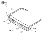
- FIG. 1A is a perspective view showing a configuration example of an electronic device.
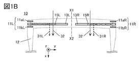
- FIG. 1B is a schematic top view showing a configuration example of an electronic device.
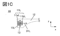
- FIG. 1C is a schematic side view showing a configuration example of the electronic device.
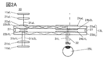
- 2A and 2B are cross-sectional views showing configuration examples of electronic devices.
- 3A and 3B are cross-sectional views showing configuration examples of electronic devices.
- 4A and 4B are cross-sectional views showing configuration examples of electronic devices.
- FIG. 7A is a perspective view showing a configuration example of an electronic device
- FIG. 7B is a schematic side view showing a configuration example of the electronic device.
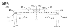
- 8A to 8D are schematic top views showing configuration examples of electronic devices.
- 9A and 9B are cross-sectional views showing configuration examples of electronic devices.
- FIG. 11A is a schematic top view showing a configuration example of an electronic device.
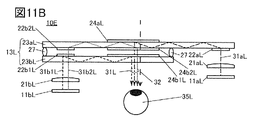
- FIG. 11B is a cross-sectional view showing a configuration example of an electronic device;
- FIG. 12A is a schematic top view showing a configuration example of an electronic device.
- FIG. 12B is a cross-sectional view showing a configuration example of an electronic device
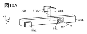
- FIG. 13A is a perspective view showing a configuration example of an electronic device
- 13B and 13C are cross-sectional views showing configuration examples of electronic devices.
- FIG. 14A is a schematic top view showing a configuration example of an electronic device.
- FIG. 14B is a cross-sectional view showing a configuration example of an electronic device;
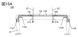
- FIG. 15A is a schematic top view showing a configuration example of an electronic device.
- FIG. 15B is a cross-sectional view showing a configuration example of an electronic device;
- FIG. 16A is a schematic top view showing a configuration example of an electronic device.
- FIG. 14A is a schematic top view showing a configuration example of an electronic device.
- 16B is a cross-sectional view showing a configuration example of an electronic device
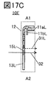
- 17A to 17C are schematic side views showing configuration examples of electronic devices.
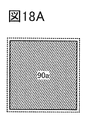
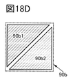
- 18A to 18E are top views showing examples of pixels.
- FIG. 19 is a cross-sectional view showing an example of a display device.
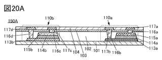
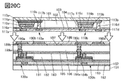
- 20A to 20C are cross-sectional views illustrating an example of a method for manufacturing a display device.
- 21A and 21B are cross-sectional views showing examples of display devices.
- 22A and 22B are cross-sectional views showing examples of display devices.
- 23A and 23B are cross-sectional views illustrating an example of a method for manufacturing a display device.
- FIG. 24 is a cross-sectional view showing an example of a display device.
- FIG. 24 is a cross-sectional view showing an example of a display device.
- 25 is a cross-sectional view showing an example of a display device.
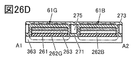
- 26A to 26D are diagrams showing configuration examples of display devices.
- 27A to 27D are diagrams showing configuration examples of display devices.
- 28A to 28C are diagrams showing configuration examples of display devices.
- 29A to 29D are diagrams illustrating configuration examples of light-emitting elements.
- 30A to 30C are diagrams illustrating examples of electronic devices.
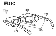
- 31A to 31C are diagrams illustrating examples of electronic devices.
- FIG. 32 is a diagram illustrating an example of an electronic device;
- film and “layer” can be interchanged depending on the case or situation.
- conductive layer can be changed to the term “conductive film.”
- insulating film can be changed to the term “insulating layer”.
- a light-emitting diode refers to a semiconductor element that emits light when a voltage is applied. Alternatively, it refers to a semiconductor element in which part of the energy when electrons and holes recombine is emitted to the outside as light.
- the light-emitting material of the light-emitting diode described in this specification is not limited, and as the light-emitting material, organic compounds (fluorescent materials, phosphorescent materials, etc.), inorganic compounds (compound semiconductor materials, quantum dot materials, etc.), etc. are used. be able to.
- a light-emitting diode using an organic compound as a light-emitting material is sometimes called an organic EL element.
- a light-emitting diode using an inorganic compound as a light-emitting material is sometimes called an inorganic EL element.
- organic EL elements and inorganic EL elements are included in light-emitting diodes.
- One embodiment of the present invention is an electronic device including a first display device, a second display device, and an optical element.
- the first display device has a first light emitting element and the second display device has a second light emitting element.
- the color of the first light emitted from the first light emitting element is different from the color of the second light emitted from the second light emitting element.
- the optical element has a first light guide plate and a second light guide plate. Note that the light guide plate in this specification and the like refers to an optical component having a function of totally reflecting light incident from an input section diffraction element described later so that the light reaches an output section diffraction element described later.
- micro LEDs As the first light emitting element and the second light emitting element.
- micro LEDs include organic LEDs in which organic materials are used as light emitting materials, and inorganic LEDs in which inorganic materials are used as light emitting materials.
- Examples of display devices using organic LEDs include so-called monolithic display devices in which organic LEDs serving as light-emitting elements are formed on transistors provided on a glass substrate or a semiconductor substrate.
- Display devices using inorganic LEDs include display devices in which inorganic LEDs provided on a compound semiconductor substrate are mounted.
- Mounting methods for inorganic LEDs include a monolithic type and a bonding type.
- the bonding type is a method of forming a display device by physically connecting separately manufactured inorganic LEDs and driving transistors for each pixel. The method is also called a pick-and-place method.
- each color for example, three colors of red (R), green (G), and blue (B)
- R red
- G green
- B blue
- the brightness of each color micro-LED depends on the material used for the light-emitting element.
- the blue (B) wavelength range is from 400 nm to less than 490 nm, and blue (B) light has at least one emission spectrum peak in this wavelength range.
- the wavelength region of green (G) is 490 nm or more and less than 580 nm, and green (G) light has at least one emission spectrum peak in this wavelength region.
- the wavelength region of red (R) is 580 nm or more and less than 700 nm, and red (R) light has at least one emission spectrum peak in this wavelength region.
- phosphorescent materials are generally used for red (R) and green (G) light emitting materials, and fluorescent materials are used for B (blue) light emitting materials.
- R red
- G green
- B blue
- Phosphorescent materials have excellent luminous efficiency, but fluorescent materials tend to have lower luminous efficiency than phosphorescent materials.
- red (R), green (G), and blue (B) are sometimes formed on compound semiconductors.
- InGaN indium gallium nitride
- the red (R) light emitting element must be formed on a compound semiconductor substrate (for example, a copper substrate) different from that of the green (G) and blue (B) light emitting elements. It is formed on a gallium nitride (GaAs) substrate).
- light-emitting elements emitting light of different colors are separately provided in two display devices, and light emitted from the two display devices is optically combined to generate an image.
- the bonding type can have a configuration in which the three sub-pixels are divided into two display devices. With such a structure, the area occupied by one pixel in one display device can be reduced as compared with the structure in which three sub-pixels are provided in one display device. Therefore, a high-resolution electronic device can be realized.
- micro LEDs with low luminous efficiency e.g., red LEDs
- micro LEDs with high luminous efficiency e.g., green LEDs and blue LEDs
- FIG. 1A is a perspective view schematically showing a configuration example of an electronic device 10 that is an electronic device of one embodiment of the present invention.
- the z-axis shown in FIG. 1A is parallel to the up-down direction (direction from feet to head) of the user (not shown), and the y-axis shown in FIG. 1A is parallel to the left-right direction of the user.
- the x-axis shown in 1A is parallel to the user's front-back direction.
- the electronic device 10 includes a pair of display devices (display device 11R and display device 11L), a housing 12, a pair of optical elements (optical element 13R and optical element 13L), and a pair of mounting portions 14. have.
- FIG. 1A is a perspective view schematically showing a configuration example of an electronic device 10 that is an electronic device of one embodiment of the present invention.
- the z-axis shown in FIG. 1A is parallel to the up-down direction (direction from feet to head) of the user (not shown), and the y
- FIG. 1A also shows a display area 15R onto which an image displayed by the display device 11R is projected, and a display area 15L onto which an image displayed by the display device 11L is projected.
- a “user” described in this specification and the like can also be referred to as a wearer of the electronic device of one embodiment of the present invention.
- arrows indicating the x-axis, y-axis, and z-axis may be attached.
- the direction along the x-axis is sometimes called the x-axis direction. Note that the forward direction and the reverse direction may not be distinguished unless explicitly stated.
- the direction along the y-axis is sometimes called the y-axis direction.
- the direction along the z-axis is sometimes called the z-axis direction.
- the x-axis, the y-axis, and the z-axis are orthogonal to each other. In other words, the x-axis direction, the y-axis direction, and the z-axis direction are directions orthogonal to each other.
- R is attached to the symbol indicating the element on the right eye side among the pair of elements. Further, among the pair of elements, the symbol indicating the element on the left eye side is denoted by "L".
- the display device 11R is a right-eye display device
- the display device 11L is a left-eye display device.
- the element refers to one or both of the pair of elements.
- the display device 11 refers to one or both of the display device 11R and the display device 11L.
- the display device 11 described in this specification and the like can be rephrased as one or both of the display device 11R and the display device 11L.
- the display device 11L when the present invention is described using the display device 11L, the display device 11L can be called the display device 11R. Further, for example, when the present invention is described using the display device 11L and the optical element 13L, the display device 11L can be called the display device 11R, and the optical element 13L can be called the optical element 13R.
- FIG. 1A shows two display areas (display area 15R and display area 15L), the present invention is not limited to this.
- the electronic device 10 may have one display area.
- the electronic device 10 has a display device 11R, a housing 12, an optical element 13R, and a pair of mounting portions 14.
- FIG. Alternatively, the electronic device 10 has a display device 11L, a housing 12, an optical element 13L, and a pair of mounting portions 14.
- FIG. 1A shows a configuration in which the electronic device 10 has a pair of optical elements (the optical element 13R and the optical element 13L), the present invention is not limited to this.
- the number of optical elements that the electronic device 10 has may be one, or three or more.
- one optical element may serve as the optical element 13R and the optical element 13L.
- the electronic device 10 can project the image displayed by the display device 11 onto the display area 15 of the optical element 13 . Further, since the optical element 13 is translucent, the user of the electronic device 10 can see the image projected onto the display area 15 superimposed on the transmitted image visually recognized through the optical element 13 .
- the electronic device 10 can be used, for example, as an AR device.
- the housing 12 may be provided with an infrared light source, an infrared light detection unit such as an infrared camera, an acceleration sensor such as a gyro sensor, and a processing unit.
- the electronic device 10 has a function of measuring the distance from the obstacle or tracked object to the electronic device 10 using the infrared light source and the infrared light detection section.
- the electronic device 10 also has a function of detecting the orientation of the user's head using the acceleration sensor.
- the electronic device 10 has a function of performing self-position estimation and environment map creation at the same time based on information including the measured distance and the detected orientation of the user's head using the processing unit.
- the electronic device 10 can perform display (so-called AR display) in which an image is superimposed on specific coordinates in the physical space.
- display so-called AR display
- a technique for simultaneously estimating the self-location and creating an environment map is called SLAM (Simultaneous Localization and Mapping).
- the housing 12 is provided with a wireless receiver or a connector to which a cable can be connected, and a video signal or the like can be supplied to the housing 12 .
- the housing 12 may be provided with a camera capable of capturing an image of the front.
- an acceleration sensor such as a gyro sensor in the housing 12 , it is possible to detect the orientation of the user's head and display an image corresponding to the orientation in the display area 15 .
- the housing 12 may be provided with a speaker or an earphone. Note that the earphones provided in the housing 12 may have a vibration mechanism that functions as bone conduction earphones.
- the housing 12 is preferably provided with a battery, which can be charged wirelessly or by wire. Further, the housing 12 may be provided with a connector to which a cable to which a power supply potential is supplied can be connected.
- the housing 12 may be provided with an infrared light source and an infrared light detector (for example, an infrared camera).
- the electronic device 10 detects infrared light emitted from an infrared light source and reflected by the user's eyeballs with an infrared light detection unit, and performs image analysis to identify the direction of the user's line of sight. may have. In other words, the electronic device 10 may have a function of performing line-of-sight tracking.
- the housing 12 may be provided with a camera that captures images of the user's eyes and their surroundings. The camera can use information on the movement of the user's eyeballs or eyelids as input means. Further, the electronic device 10 may have a function of identifying the direction of the user's line of sight by analyzing the image of the user's eyes and the surroundings captured by the camera.
- FIG. 1B is a schematic top view of electronic device 10 viewed from above the user
- FIG. 1C is a schematic side view of electronic device 10 viewed from the left side of the user. Note that FIG. 1C shows only the elements on the left-eye side of the electronic device 10 for clarity of illustration.
- the housing 12 is provided with a display device 11R, a display device 11L, an optical element 13R, and an optical element 13L.
- the display device 11R and the display device 11L are arranged in line-symmetrical positions with respect to the dashed-dotted line X1-X2 shown in FIG. 1B (the center line that divides the horizontal direction of the drawing) as an axis of symmetry.
- the display device 11R has a display device 11aR and a display device 11bR.
- the optical element 13R is provided between the display device 11aR and the display device 11bR.
- the display device 11bR is arranged on the user side (wearer's head side).
- the display device 11L has a display device 11aL and a display device 11bL.
- the optical element 13L is provided between the display device 11aL and the display device 11bL.
- the display device 11bL is arranged on the user side.
- the display device 11aR corresponds to the first display device described above, and the display device 11bR corresponds to the second display device described above.
- the display device 11aL corresponds to the first display device described above, and the display device 11bL corresponds to the second display device described above.
- the display device 11aL has an area overlapping the display device 11bL via the optical element 13L.
- the display device 11aR has a region that overlaps with the display device 11bR via the optical element 13R.
- the display device 11aL and the display device 11bL are located at the same or approximately the same height as the display area 15L.
- display device 11aR and display device 11bR are located at the same or approximately the same height as display area 15R.
- the display device 11aR and the display device 11aL each have a first light emitting element
- the display device 11bR and the display device 11bL each have a second light emitting element.
- the color of the first light emitted from the first light emitting element and the color of the second light emitted from the second light emitting element are preferably different.
- each of the display device 11bR and the display device 11bL further includes a third light emitting element.
- the color of the third light emitted from the third light emitting element is preferably different from the color of the first light described above and the color of the second light described above.
- paths of light may be indicated by dotted line arrows, dashed line arrows, or dashed line arrows.
- Dotted line arrows, dashed line arrows, and one-dot chain line arrows shown in the drawings are schematically shown to facilitate the explanation of the present invention, and do not necessarily indicate actual optical paths.
- each of the display device 11aL and the display device 11bL enters the optical element 13L. Inside the optical element 13L, the light repeats total reflection at the end face of the optical element 13L and reaches the display area 15L. The light that has reached the display area 15L is taken out of the optical element 13L, so that the user can see light 31L that is a combination of the light emitted from the display device 11aL and the light emitted from the display device 11bL, and Both of the light 32 transmitted through the optical element 13L can be visually recognized.
- the method of projecting an image onto the display region 15R is the same as the method of projecting an image onto the display region 15L, so the explanation is omitted.
- the light 31R shown in FIG. 1B is the combined light of the light emitted from the display device 11aR and the light emitted from the display device 11bR.
- a diffraction element is preferably used for making light incident on the optical element 13 or extracting light from the optical element 13 .
- Diffractive elements are classified into transmissive and reflective types.
- diffraction elements include diffraction gratings, holographic optical elements, half mirrors, and the like.
- Diffraction gratings include transmission type diffraction gratings and reflection type diffraction gratings.
- Holograms displayed by holographic optical elements include embossed (also called relief) holograms and volume holograms. Volume holograms are classified into transmission type and reflection type.
- a diffraction grating or a holographic optical element as the diffraction element.
- the optical element 13 can be thinned by using a diffraction grating or a holographic optical element. Therefore, miniaturization of the electronic device 10 can be achieved. Further, it is more preferable to use a diffraction grating as the diffraction element. Diffraction gratings can be fabricated using, for example, nanoimprinting. Therefore, the manufacturing cost of the electronic device 10 can be suppressed as compared with the case of using the holographic optical element.
- FIG. 2A is a cross-sectional view showing an example of the configuration of the electronic device 10 on the left-eye side.
- the electronic device 10 shown in FIG. 2A has a display device 11aL, a display device 11bL, and an optical element 13L on the left eye side.
- the optical element 13L is provided between the display device 11aL and the display device 11bL.
- the display device 11bL is arranged on the user side.
- the display device 11aL shown in FIG. 2A emits light 31aL.
- the color of the light emitted by the display device 11aL is not limited to one color, and may be two or more colors.
- the display device 11bL shown in FIG. 2A emits light 31b1L and light 31b2L.
- the color of the light 31b1L and the color of the light 31b2L are different.
- the colors of light emitted by the display device 11bL are not limited to two colors, and may be one color or three or more colors.
- the optical element 13L has two light guide plates (light guide plate 23aL and light guide plate 23bL).
- the light guide plate 23aL is arranged between the display device 11aL and the light guide plate 23bL. Further, the light guide plate 23bL is arranged between the display device 11bL and the light guide plate 23aL.
- the number of light guide plates included in the optical element 13L may be one, or may be three or more. Also, one light guide plate may serve as both the light guide plate 23aL and one of the two light guide plates included in the optical element 13R. Also, one light guide plate may serve as both the light guide plate 23bL and the other of the two light guide plates included in the optical element 13R.
- the light guide plate 23aL corresponds to the above-described first light guide plate
- the light guide plate 23bL corresponds to the above-described second light guide plate.
- the optical element 13L has a spacer 27.
- the spacer 27 is provided between the light guide plate 23aL and the light guide plate 23bL.
- an air layer is provided on the surface of the light guide plate 23aL and the surface of the light guide plate 23bL.
- the air layer can totally reflect the light incident on the light guide plate 23aL or the light guide plate 23bL.
- FIG. 2A shows a configuration in which two spacers 27 are provided between the light guide plate 23aL and the light guide plate 23bL, the number of spacers 27 is not limited to this. good too.
- the optical element 13L may have a low refractive index layer that satisfies the conditions for total reflection of the light incident on the light guide plate 23aL or the light guide plate 23bL. At this time, the low refractive index layer is provided between the light guide plate 23aL and the light guide plate 23bL.
- the optical element 13L includes three input diffraction elements (input diffraction element 22aL, input diffraction element 22b1L, and input diffraction element 22b2L) and three output diffraction elements (output diffraction element 24aL, output diffraction element 24aL). 24b1L, and output diffractive element 24b2L).
- the numbers of input diffraction elements and output diffraction elements may be appropriately adjusted according to the number of colors of light emitted from the display device 11aL and the display device 11bL. For example, if the number of colors of light emitted from the display device 11aL and the display device 11bL is two, the optical element 13L may have two input diffractive elements and two output diffractive elements.
- the input part diffraction element and the output part diffraction element can function as spacers 27 .
- an input diffractive element and/or an output diffractive element provided between the light guide plate 23aL and the light guide plate 23bL can function as the spacer 27.
- the spacer 27 may not be provided.
- the input section diffraction element and the output section diffraction element may be formed directly on the light guide plate, or may be formed separately from the light guide plate and attached to the light guide plate.
- the input section diffraction element 22aL has a function of causing the light 31aL to enter the light guide plate 23aL or the light guide plate 23bL.
- the input section diffraction element 22b1L has a function of causing the light 31b1L to enter the light guide plate 23aL or the light guide plate 23bL.
- the input section diffraction element 22b2L has a function of causing the light 31b2L to enter the light guide plate 23aL or the light guide plate 23bL.
- the output diffraction element 24aL has a function of emitting the light 31aL incident on the light guide plate 23aL or the light guide plate 23bL to the outside of the light guide plate 23aL or the light guide plate 23bL.
- the output diffraction element 24b1L has a function of emitting the light 31b1L incident on the light guide plate 23aL or the light guide plate 23bL to the outside of the light guide plate 23aL or the light guide plate 23bL.
- the output diffraction element 24b2L has a function of emitting the light 31b2L incident on the light guide plate 23aL or the light guide plate 23bL to the outside of the light guide plate 23aL or the light guide plate 23bL.
- the input diffraction element 22aL and the output diffraction element 24aL are provided on the display device 11aL side of the light guide plate 23aL.
- the input diffraction element 22b1L and the output diffraction element 24b1L are provided on the display device 11aL side surface of the light guide plate 23bL.
- the input diffraction element 22b2L and the output diffraction element 24b2L are provided on the display device 11bL side surface of the light guide plate 23aL.
- the input section diffraction element 22b1L and the input section diffraction element 22b2L may function as spacers 27.
- the output diffraction element 24b1L and the output diffraction element 24b2L may function as spacers 27.
- the spacer 27 may not be provided.
- Light 31aL emitted from the display device 11aL is incident on the light guide plate 23aL by the input section diffraction element 22aL. Inside the light guide plate 23aL, the light 31aL repeats total reflection at the end surface of the light guide plate 23aL and reaches the output diffraction element 24aL. The light 31aL reaching the output diffraction element 24aL is emitted toward the user's left eye 35L by the output diffraction element 24aL.
- the input diffraction element 22aL is a transmission diffraction element and the output diffraction element 24aL is a reflection diffraction element.
- the light 31b1L emitted from the display device 11bL is incident on the light guide plate 23bL by the input section diffraction element 22b1L. Inside the light guide plate 23bL, the light 31b1L repeats total reflection at the end surface of the light guide plate 23bL and reaches the output diffraction element 24b1L. The light 31b1L reaching the output diffraction element 24b1L is emitted toward the user's left eye 35L by the output diffraction element 24b1L. In the configuration shown in FIG. 2A, the input diffraction element 22b1L and the output diffraction element 24b1L are reflective diffraction elements.
- the light 31b2L emitted from the display device 11bL is incident on the light guide plate 23aL by the input section diffraction element 22b2L. Inside the light guide plate 23aL, the light 31b2L repeats total reflection at the end surface of the light guide plate 23aL and reaches the output diffraction element 24b2L. The light 31b2L reaching the output diffraction element 24b2L is emitted toward the user's left eye 35L by the output diffraction element 24b2L.
- the input diffraction element 22b2L and the output diffraction element 24b2L are transmissive diffraction elements.
- the user can view both the light 31L, which is the combination of the light 31aL and the light 31b2L emitted from the light guide plate 23aL and the light 31b1L emitted from the light guide plate 23bL, and the light 32 transmitted through the optical element 13L. can be visually recognized. Since an image is formed by synthesizing the light 31aL and the light 31b2L emitted from the light guide plate 23aL and the light 31b1L emitted from the light guide plate 23bL, the light 31L can be rephrased as an image.
- the types of the input section diffraction element and the output section diffraction element (transmission type or reflection type) and the arrangement of the input section diffraction element and the output section diffraction element are not limited to the above. It may be appropriately selected depending on the distance between the partial diffraction elements, the thickness of the light guide plate 23aL and the light guide plate 23bL, and the like.
- an appropriate image can be obtained by aligning the light 31aL with the light 31b1L and the light 31b2L.
- the alignment may be performed based on alignment marks provided on the display device 11aL and the light guide plate 23aL, and based on alignment marks provided on the display device 11bL and the light guide plate 23bL.
- the alignment of the display device 11aL, the display device 11bL, the light guide plate 23aL, and the light guide plate 23bL is performed by synthesizing the alignment mark images displayed on the display device 11aL and the display device 11bL, respectively, using the optical element 13L. You can do this while checking the image.
- a lens 21aL may be provided between the display device 11aL and the light guide plate 23aL.
- a lens 21bL may be provided between the display device 11bL and the light guide plate 23bL.
- a collimator lens, a microlens array, or the like can be used as the lens 21aL and the lens 21bL.
- the lens 21aL and the lens 21bL may be formed directly on the display device 11aL and the display device 11bL, respectively.
- the lens 21aL and the lens 21bL may be formed separately from the display device 11aL and the display device 11bL, and bonded to the display device 11aL and the display device 11bL, respectively.
- the housing 12 (not shown in FIG. 2A) has a mechanism for adjusting the distance between the lens 21aL and the display device 11aL, the distance between the lens 21bL and the display device 11bL, or the angles of these. is preferred. This makes it possible to adjust the focus, enlarge or reduce the image, and the like.
- one or both of the lens 21aL and the display device 11aL and one or both of the lens 21bL and the display device 11bL may be configured to be movable in the optical axis direction.
- the configuration on the left-eye side and the configuration on the right-eye side of electronic device 10 are symmetrical about the dashed-dotted line X1-X2 shown in FIG. 1B (the center line dividing the horizontal direction of the figure). is placed in the position of That is, the configuration of the left-eye side of the electronic device 10 that is inverted with respect to the dashed-dotted line X1-X2 shown in FIG. 1B is the configuration of the right-eye side of the electronic device 10 . Therefore, for the details of the method of projecting an image onto the display area for the right eye, the detailed description of the method of projecting an image onto the display area for the left eye can be considered.
- the configuration of the left-eye side of the electronic device 10 for projecting an image on the left-eye display area is not limited to the configuration shown in FIG. 2A.
- the configuration on the left eye side of the electronic device 10 may be the configuration shown in FIG. 2B, the configuration shown in FIG. 3A, or the configuration shown in FIG. 3B.
- FIG. 2B is a cross-sectional view showing another example of the configuration of the electronic device 10 on the left-eye side.
- the electronic device 10 shown in FIG. 2B is shown in FIG. 2A in that the input diffraction element 22b2L and the output diffraction element 24b2L are provided on the surface of the light guide plate 23bL on the display device 11bL side on the left eye side. It is different from the electronic device 10 .
- the paths of the light 31aL and the light 31b1L are the same as those described with reference to FIG. 2A, so the description is omitted.
- the light 31b2L emitted from the display device 11bL is incident on the light guide plate 23bL by the input section diffraction element 22b2L. Inside the light guide plate 23bL, the light 31b2L repeats total reflection at the end surface of the light guide plate 23bL and reaches the output diffraction element 24b2L. The light 31b2L reaching the output diffraction element 24b2L is emitted toward the user's left eye 35L by the output diffraction element 24b2L. Also in the configuration shown in FIG. 2B, the input diffraction element 22aL and the output diffraction element 24aL are transmissive diffraction elements.
- an image can be projected on the display area on the left eye side.
- FIG. 3A is a cross-sectional view showing another example of the configuration of the electronic device 10 on the left-eye side.
- the electronic device 10 shown in FIG. 3A is different from the electronic device 10 shown in FIG. 2A in that the display device 11aL is arranged on the user's left eye side.
- the display device 11bL is arranged on the side facing the user via the optical element 13L
- the light guide plate 23aL is arranged on the user side
- a light guide plate 23bL is arranged between the display device 11bL and the light guide plate 23aL.
- the output diffraction element 24aL is provided on the surface of the light guide plate 23aL facing the display device 11bL, and the output diffraction element 24b1L is provided on the display device of the light guide plate 23bL.
- the output diffraction element 24b2L is provided on the surface of the light guide plate 23aL facing the display device 11aL.
- the paths of the light 31aL, the light 31b1L, and the light 31b2L are the same as those described with reference to FIG. 2A, so the description is omitted. Also, the type (transmissive type or reflective type) of each of the three input section diffraction elements and the three output section diffraction elements shown in FIG. 3A is the same as the content explained using FIG. 2A.
- an image can be projected on the display area on the left eye side.
- FIG. 3B is a cross-sectional view showing another example of the configuration of the electronic device 10 on the left-eye side.
- the input diffraction element 22b2L is provided on the surface of the light guide plate 23bL facing the display device 11bL
- the output diffraction element 24b2L is provided on the display device 11aL side of the light guide plate 23bL. It is different from the electronic device 10 shown in FIG. 3A in that it is provided on the surface of the .
- the paths of the light 31aL, the light 31b1L, and the light 31b2L are the same as those described with reference to FIG. 2B, so the description is omitted. Also, the type (transmissive type or reflective type) of each of the three input section diffraction elements and the three output section diffraction elements shown in FIG. 3B is the same as the content described using FIG. 2B.
- an image can be projected on the display area on the left eye side.
- FIG. 1B and the like show an example in which the display device 11R is arranged on the inner side of the user's right eye and the display device 11L is arranged on the inner side of the user's left eye. , and the display device 11L may be placed on the inner corner side of the user's left eye.
- the display device 11aL and the display device 11bL are arranged to face each other via the optical element 13L.
- the image displayed on the display device 11aL and the image displayed on the display device 11bL have a left-right (horizontal) inversion relationship.
- a full-color image can be generated by synthesizing the image displayed on the display device 11aL and the image displayed on the display device 11bL, and the full-color image can be projected onto the display area 15L. can be done.
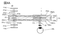
- FIG. 4A is a cross-sectional view showing an example of the configuration of the electronic device 10 on the left-eye side.
- the electronic device 10 shown in FIG. 4A differs from the electronic device shown in FIG. 2A in that the display device 11aL emits light 31aL and light 31cL.
- the light 31cL is emitted from a light emitting element different from the first light emitting element. That is, the display device 11aL further has a fourth light emitting element that emits the light 31cL.
- the electronic device 10 shown in FIG. 4A differs from the electronic device shown in FIG.
- the 2A in that it has an input diffraction element 22cL and an output diffraction element 24cL.
- the input diffraction element 22cL and the output diffraction element 24cL are provided on the surface of the light guide plate 23bL facing the display device 11bL. It is different from the electronic device 10 .
- the color of the light 31cL is different from the colors of the light 31aL, the light 31b1L, and the light 31b2L. If the color of the light 31aL is red, the color of the light 31b1L is one of green and blue, and the color of the light 31b2L is the other of green and blue, the color of the light 31cL may be yellow, for example. Note that the color of the light 31cL is not limited to yellow, and may be any one of cyan, magenta, white, and the like.
- the input part diffraction element 22cL is of reflection type, and the output part diffraction element 24cL is of transmission type.
- the types (transmission type or reflection type) of the other three input section diffraction elements and the other three output section diffraction elements shown in FIG. 4A are the same as those described with reference to FIG. 2A.
- the paths of the light 31aL, the light 31b1L, and the light 31b2L are the same as those described with reference to FIG. 2A, so the description is omitted.
- the light 31cL emitted from the display device 11aL is incident on the light guide plate 23bL by the input section diffraction element 22cL. Inside the light guide plate 23bL, the light 31cL repeats total reflection at the end surface of the light guide plate 23bL and reaches the output diffraction element 24cL. The light 31cL reaching the output diffraction element 24cL is emitted toward the user's left eye 35L by the output diffraction element 24cL.
- the user can obtain light 31L, which is a combination of light 31aL and light 31b2L emitted from the light guide plate 23aL and light 31b1L and light 31cL emitted from the light guide plate 23bL, and light transmitted through the optical element 13L. 32 are both visible. Since an image is formed by synthesizing the light 31aL and the light 31b2L emitted from the light guide plate 23aL and the light 31b1L and the light 31cL emitted from the light guide plate 23bL, the light 31L can be rephrased as an image. can.
- an image can be projected on the display area on the left eye side.
- FIG. 4B is a cross-sectional view showing an example of the configuration of the electronic device 10 on the left-eye side.
- the electronic device 10 shown in FIG. 4B differs from the electronic device shown in FIG. 2A in that the display device 11bL emits light 31b1L, light 31b2L, and light 31dL.
- the light 31dL is emitted from a light emitting element different from the second light emitting element and the third light emitting element. That is, the display device 11aL further has a fourth light emitting element that emits the light 31dL.
- the electronic device 10 shown in FIG. 4B differs from the electronic device shown in FIG. 2A in that it has an input diffraction element 22dL and an output diffraction element 24dL.
- the input diffraction element 22dL and the output diffraction element 24dL are provided on the surface of the light guide plate 23bL on the display device 11bL side. It is different from the electronic device 10 .
- the color of the light 31dL is different from each of the colors of the light 31aL, the light 31b1L, and the light 31b2L. If the color of the light 31aL is red, the color of the light 31b1L is one of green and blue, and the color of the light 31b2L is the other of green and blue, the color of the light 31dL may be white, for example. Note that the color of the light 31dL is not limited to white, and may be any one of cyan, magenta, yellow, and the like.
- the input part diffraction element 22dL and the output part diffraction element 24cL are of transmissive type.
- the types (transmission type or reflection type) of the other three input section diffraction elements and the other three output section diffraction elements shown in FIG. 4B are the same as those described with reference to FIG. 2A.
- the paths of the light 31aL, the light 31b1L, and the light 31b2L are the same as those described with reference to FIG. 2A, so the description is omitted.
- the light 31dL emitted from the display device 11bL is incident on the light guide plate 23bL by the input section diffraction element 22dL. Inside the light guide plate 23bL, the light 31dL repeats total reflection at the end face of the light guide plate 23bL and reaches the output diffraction element 24dL. The light 31dL reaching the output diffraction element 24dL is emitted toward the user's left eye 35L by the output diffraction element 24dL.
- the user can view the light 31aL and the light 31b2L emitted from the light guide plate 23aL, the light 31b1L and the light 31dL emitted from the light guide plate 23bL, and the light transmitted through the optical element 13L. 32 are both visible. Since an image is formed by synthesizing the light 31aL and the light 31b2L emitted from the light guide plate 23aL and the light 31b1L and the light 31dL emitted from the light guide plate 23bL, the light 31L can be rephrased as an image. can.
- an image can be projected on the display area on the left eye side.
- the display device 11aL and the display device 11bL are positioned at the same or approximately the same height as the display area when viewed from the side of the user. and the height of one or both of the display device 11bL may be different from the height of the display area.
- an electronic device in which one or both of the display devices 11aL and 11bL and the height of the display area are different will be described with reference to FIGS. 5 and 6.
- FIG. 5 and 6 an electronic device in which one or both of the display devices 11aL and 11bL and the height of the display area are different will be described with reference to FIGS. 5 and 6.
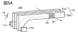
- FIG. 5A is a perspective view showing an example of the left eye side configuration of the electronic device 10A.
- the z-axis shown in FIG. 5A is parallel to the vertical direction (direction from feet to head) of the user (not shown), and the y-axis shown in FIG. 5A is parallel to the lateral direction of the user.
- the x-axis shown in 5A is parallel to the user's front-back direction.
- some elements are omitted for clarity of the drawing.
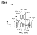
- FIG. 5B is a cross-sectional view showing an example of the left-eye configuration of the electronic device 10A shown in FIG. 5A, viewed from the left side of the user.
- FIG. 5B corresponds to the xz plane including display device 11aL and display device 11bL.
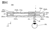
- FIG. 5C is a cross-sectional view showing an example of the configuration of the left-eye side of the electronic device 10A as viewed from above the user.
- FIG. 5C corresponds to the xy plane including the display area 15L (not shown).
- the electronic device 10A shown in FIGS. 5A to 5C differs from the electronic device 10 shown in FIG. 2A in that the height of the display device 11aL and the display device 11bL is lower than the height of the display area 15L on the left eye side. At this time, the display device 11aL has a region that overlaps with the display device 11bL via the optical element 13L. Further, the electronic device 10A shown in FIGS. 5A to 5C differs from the electronic device shown in FIG. 2A in that it has a diffraction element 25aL, a diffraction element 25b1L, and a diffraction element 25b2L.
- the diffraction element 25aL is provided on the display device 11aL side surface of the light guide plate 23aL
- the diffraction element 25b1L is provided on the display device 11aL side surface of the light guide plate 23bL
- the diffraction element 25b2L is provided on the light guide plate 11aL side.
- 23aL is provided on the surface of the display device 11bL side.
- the diffraction element 25aL, the diffraction element 25b1L, and the diffraction element 25b2L are of a reflective type.
- the type (transmissive type or reflective type) of each of the three input section diffraction elements shown in FIG. 5B is the same as that described using FIG. 2A.
- the type (transmissive type or reflective type) of each of the three output section diffraction elements shown in FIG. 5C is the same as that described using FIG. 2A.
- Light 31aL emitted from the display device 11aL is incident on the light guide plate 23aL by the input section diffraction element 22aL. Inside the light guide plate 23aL, the light 31aL repeats total reflection at the end face of the light guide plate 23aL, travels in the z-axis direction, and reaches the diffraction element 25aL.
- the light 31aL reaching the diffraction element 25aL changes its traveling direction to the y-axis direction by the diffraction element 25aL, repeats total reflection at the end face of the light guide plate 23aL, and reaches the output part diffraction element 24aL.
- the light 31aL reaching the output diffraction element 24aL is emitted toward the user's left eye 35L by the output diffraction element 24aL.
- the light 31b1L emitted from the display device 11bL is incident on the light guide plate 23bL by the input section diffraction element 22b1L. Inside the light guide plate 23bL, the light 31b1L repeats total reflection at the end surface of the light guide plate 23bL, travels in the z-axis direction, and reaches the diffraction element 25b1L.
- the light 31b1L reaching the diffraction element 25b1L changes its traveling direction to the y-axis direction by the diffraction element 25b1L, repeats total reflection at the end face of the light guide plate 23bL, and reaches the output part diffraction element 24b1L.
- the light 31b1L reaching the output diffraction element 24b1L is emitted toward the user's left eye 35L by the output diffraction element 24b1L.
- the light 31b2L emitted from the display device 11bL is incident on the light guide plate 23aL by the input section diffraction element 22b2L. Inside the light guide plate 23aL, the light 31b2L repeats total reflection at the end surface of the light guide plate 23aL, travels in the z-axis direction, and reaches the diffraction element 25b2L.
- the light 31b2L reaching the diffraction element 25b2L changes its traveling direction to the y-axis direction by the diffraction element 25b2L, repeats total reflection at the end face of the light guide plate 23aL, and reaches the output part diffraction element 24b2L.
- the light 31b2L reaching the output diffraction element 24b2L is emitted toward the user's left eye 35L by the output diffraction element 24b2L.
- an image can be projected on the display area on the left eye side.
- FIG. 6A is a perspective view showing another example of the left eye side configuration of the electronic device 10A.
- the z-axis shown in FIG. 6A is parallel to the up-down direction (direction from feet to head) of the user (not shown), and the y-axis shown in FIG. 6A is parallel to the left-right direction of the user.
- the x-axis shown in 6A is parallel to the user's front-back direction.
- some elements are omitted for clarity of illustration.
- FIG. 6B is a cross-sectional view showing an example of the left-eye configuration of the electronic device 10A shown in FIG. 6A, viewed from the left side of the user.
- FIG. 6B corresponds to the xz plane including display device 11aL and display device 11bL.
- FIG. 6C is a cross-sectional view showing an example of the configuration of the left-eye side of the electronic device 10A as viewed from above the user.
- FIG. 6C corresponds to the xy plane including the display device 11bL and the display area 15L (not shown).
- the electronic device 10A shown in FIGS. 6A to 6C differs from the electronic device 10 shown in FIG. 2A in that the height of the display device 11aL is lower than the height of the display area 15L on the left eye side.
- the display device 11aL does not overlap with 11bL via the optical element 13L.
- the electronic device 10A shown in FIGS. 6A to 6C differs from the electronic device shown in FIG. 2A in that it has a diffraction element 25aL.
- the electronic device 10A shown in FIGS. 6A to 6C is different from the electronic device 10A shown in FIGS. 5A to 5C in that the height of the display device 11bL and the height of the display area 15L are the same or substantially the same on the left eye side. is different. Further, the electronic device 10A shown in FIGS. 6A to 6C differs from the electronic device 10A shown in FIGS. 5A to 5C in that it does not have the diffraction element 25b1L and the diffraction element 25b2L.
- the type of the diffraction element 25aL is assumed to be a reflection type.
- the type (transmissive type or reflective type) of each of the three input section diffraction elements shown in FIG. 6B is the same as that described using FIG. 2A.
- the type (transmissive type or reflective type) of each of the three output section diffraction elements shown in FIG. 5C is the same as that described using FIG. 2A.
- the description of the path of the light 31aL is omitted because it is the same as that described using FIGS. 5B and 5C. Further, since the paths of the light 31b1L and the light 31b2L are the same as those described with reference to FIG. 2A, description thereof will be omitted.
- an image can be projected on the display area on the left eye side.
- ⁇ Configuration example 3> 1A to 6B show a configuration in which the display device 11R is arranged on the right side of the optical element 13R (on the inner side of the right eye), and the display device 11L is arranged on the left side of the optical element 13L (on the inner side of the left eye).
- the arrangement of the display device 11R and the display device 11L is not limited to this.
- the display device 11R and the display device 11L may be arranged above the optical element 13R and the optical element 13L, respectively.
- an electronic device in which the display device 11R and the display device 11L are arranged above the optical element 13R and the optical element 13L, respectively, will be described with reference to FIG.
- FIG. 7A is a perspective view schematically showing a configuration example of the electronic device 10B.
- FIG. 7B is a schematic cross-sectional view of the portion indicated by the dashed-dotted line A1-A2 in FIG. 7A viewed from the right side of the user.
- FIG. 7B only the elements on the left-eye side of the electronic device 10B are illustrated for clarity of illustration.
- the schematic cross-sectional view is rotated leftward by 90 degrees (rotated by 90 degrees with respect to the y-axis) in order to facilitate the subsequent description.
- the electronic device 10B shown in FIGS. 7A and 7B differs from the electronic device 10 shown in FIG. 1A and the like in that the display device 11R and the display device 11L are arranged above the optical element 13R and the optical element 13L, respectively.
- the display device 11aL has a region that overlaps with the display device 11bL via the optical element 13L.
- the display device 11aR has a region that overlaps with the display device 11bR via the optical element 13R.
- the arrangement of the elements constituting the electronic device 10B viewed from the y-axis direction and the arrangement of the elements constituting the electronic device 10 viewed from the z-axis direction are equivalent.
- the arrangement of the elements constituting the electronic device 10B viewed from the side of the user is the same as the arrangement of the elements constituting the electronic device 10 or the electronic device 10A viewed from above the user. Therefore, for the details of the configuration example of the electronic device 10B, the contents described using FIGS. 2 to 6 can be referred to.
- the z-axis shown in FIG. 1B is regarded as the y-axis shown in FIG. 7B
- the y-axis direction shown in FIG. 1B is regarded as the opposite direction of the z-axis direction shown in FIG. 7B.
- the contents described with reference to FIGS. 2 to 6 can be referred to.
- the electronic device 10B has a band-like fixture 17 instead of the pair of mounting portions 14 of the electronic device 10 shown in FIG. 1A.
- the electronic device 10 ⁇ /b>B may have a pair of mounting portions 14 instead of the band-like fixture 17 .
- the electronic device 10 may have a band-like fixture 17 instead of the pair of mounting portions 14 .
- FIG. 7A and the like show an example in which the display device 11R and the display device 11L are arranged above the optical element 13R and the optical element 13L, respectively, the present invention is not limited to this.
- the display device 11R and the display device 11L may be arranged below the optical element 13R and the optical element 13L, respectively.
- one of the display device 11R and the display device 11L may be arranged above the optical element, and the other of the display device 11R and the display device 11L may be arranged below the optical element.
- the display device 11aR and the display device 11bR are arranged on the right side of the optical element 13R (on the inner side of the right eye), and the display devices 11aL and 11bL are arranged on the left side of the optical element 13L (on the inner side of the left eye).
- the arrangement of the display device 11aR, the display device 11bR, the display device 11aL, and the display device 11bL is not limited to this.
- one of the display devices 11aR and 11bR is arranged on the right side of the optical element 13R (on the inner side of the right eye), and the other of the display devices 11aR and 11bR is arranged on the left side of the optical element 13R (on the inner side of the right eye).
- One of the display devices 11aL and 11bL is arranged on the left side of the optical element 13L (on the inner side of the left eye), and the other of the display devices 11aL and 11bL is arranged on the right side of the optical element 13L (on the inner side of the left eye).
- the display device 11aR does not overlap the display device 11bR via the optical element 13R.
- the display device 11aL does not overlap the display device 11bL via the optical element 13L.
- an electronic device in which at least one of the display device 11aR, the display device 11bR, the display device 11aL, and the display device 11bL is arranged differently from the electronic device 10 will be described with reference to FIGS. 8A to 9B.
- FIG. 8A is a schematic top view of the electronic device 10C as seen from above the user.
- the electronic device 10C shown in FIG. 8A is characterized in that the display device 11aR is arranged on the left side of the optical element 13R (inner eye side of the right eye), and the display device 11aL is arranged on the right side of the optical element 13L (inner eye side of the left eye). , is different from the electronic device 10 shown in FIG. 1B.
- the configuration on the left-eye side and the configuration on the right-eye side of the electronic device 10C shown in FIG. 8A are line-symmetrical about the dashed-dotted line X1-X2 (the center line dividing the horizontal direction of the figure) shown in FIG. 8A. placed in position.
- FIG. 9A is a cross-sectional view showing an example of the left eye side configuration of the electronic device 10C.
- the electronic device 10C shown in FIG. 9A differs from the electronic device 10 shown in FIG. 2A in that the display device 11aL is arranged on the right side of the optical element 13L (on the inner corner of the left eye).
- the paths of the light 31aL, the light 31b1L, and the light 31b2L are the same as those described with reference to FIG. 2A, so description thereof will be omitted.
- the types (transmission type or reflection type) of the three input section diffraction elements and the three output section diffraction elements shown in FIG. 9A are the same as those described with reference to FIG. 2A.
- an image can be projected on the display area on the left eye side.
- FIG. 9A shows a configuration in which the light guide plate 23aL is arranged between the display device 11aL and the light guide plate 23bL, and the light guide plate 23bL is arranged between the display device 11bL and the light guide plate 23aL.
- the aspect is not limited to this.
- the light guide plate 23aL may be arranged between the display device 11bL and the light guide plate 23bL, and the light guide plate 23bL may be arranged between the display device 11aL and the light guide plate 23aL.
- FIG. 9B is a cross-sectional view showing another example of the left eye side configuration of the electronic device 10C.
- the electronic device 10C shown in FIG. 9B has the light guide plate 23aL arranged between the display device 11bL and the light guide plate 23bL, and the light guide plate 23bL arranged between the display device 11aL and the light guide plate 23aL. It differs from the electronic device 10C shown in 9A.
- the paths of the light 31aL, the light 31b1L, and the light 31b2L are the same as those described with reference to FIG. 2B, so the description is omitted. Also, the type (transmissive type or reflective type) of each of the three input section diffraction elements and the three output section diffraction elements shown in FIG. 9B is the same as the content described using FIG. 2B.
- an image can be projected on the display area on the left eye side.
- the distance between the display device 11aL and the display device 11bL in the x-axis direction can be narrowed. Therefore, it is possible to reduce the size or thickness of the electronic device 10C.
- the configuration on the left-eye side and the configuration on the right-eye side of the electronic device 10C shown in FIG. 8A are symmetrical about the dashed-dotted line X1-X2 (the center line dividing the horizontal direction of the figure) shown in FIG. 8A. They are arranged in symmetrical positions about the axis. That is, the configuration of the right-eye side of the electronic device 10C shown in FIG. 8A is the same as the configuration of the left-eye side of the electronic device 10C that is inverted with the dashed-dotted line X1-X2 shown in FIG. 8A as the axis of symmetry.
- FIG. 8B is a schematic top view of the electronic device 10C as seen from above the user.
- the electronic device 10C shown in FIG. 8B is characterized in that the display device 11bR is arranged on the left side of the optical element 13R (on the inner side of the right eye), and the display device 11bL is arranged on the right side of the optical element 13L (on the inner side of the left eye). , is different from the electronic device 10 shown in FIG. 1B.
- the configuration on the left-eye side and the configuration on the right-eye side of the electronic device 10C shown in FIG. 8B are symmetrical with respect to the dashed-dotted line X1-X2 (the center line dividing the horizontal direction of the figure) shown in FIG. 8B. placed in position.
- the configuration of the right-eye side of the electronic device 10C shown in FIG. 8B is equivalent to the configuration of the left-eye side of the electronic device 10C shown in FIG. 8A, and the configuration of the left-eye side of the electronic device 10C shown in FIG. This is the same as the configuration on the right eye side of the electronic device 10C shown in FIG. 8A. Therefore, the details of the configuration of the electronic device 10C shown in FIG. 8B and the details of the method of projecting an image onto the display area can be referred to the contents described with reference to FIGS. 9A and 9B.
- FIG. 8C is a schematic top view of the electronic device 10C as seen from above the user.
- the electronic device 10C shown in FIG. 8C is characterized in that the display device 11aR is arranged on the left side of the optical element 13R (on the inner side of the right eye), and the display device 11bL is arranged on the right side of the optical element 13L (on the inner side of the left eye). , is different from the electronic device 10 shown in FIG. 1B.
- the configuration on the left eye side and the configuration on the right eye side of the electronic device 10C shown in FIG. 8C are the same. Therefore, the element forming the left eye side and the element forming the right eye side can be manufactured in common. Therefore, the manufacturing cost can be reduced.
- the configuration of the left-eye side and the configuration of the right-eye side of the electronic device 10C shown in FIG. 8C are equivalent to the configuration of the right-eye side of the electronic device 10C shown in FIG. 8A. Therefore, the details of the configuration of the electronic device 10C shown in FIG. 8C and the details of the method of projecting an image onto the display area can be referred to the contents described with reference to FIGS. 9A and 9B.
- FIG. 8D is a schematic top view of the electronic device 10C as seen from above the user.
- the electronic device 10C shown in FIG. 8D is characterized in that the display device 11bR is arranged on the left side of the optical element 13R (inner eye side of the right eye), and the display device 11aL is arranged on the right side of the optical element 13L (inner eye side of the left eye). , is different from the electronic device 10 shown in FIG. 1B.
- the configuration on the left eye side and the configuration on the right eye side of the electronic device 10C shown in FIG. 8D are the same. Therefore, the element forming the left eye side and the element forming the right eye side can be manufactured in common. Therefore, the manufacturing cost can be reduced.
- the left-eye side configuration and right-eye side configuration of the electronic device 10C shown in FIG. 8D are equivalent to the left-eye side configuration of the electronic device 10C shown in FIG. 8A. Therefore, the details of the configuration of the electronic device 10C shown in FIG. 8D and the details of the method of projecting an image onto the display area can be referred to the contents described with reference to FIGS. 9A and 9B.
- One aspect of the present invention may combine the configurations shown in FIGS. 1A to 9B.
- the height of the display devices 11aR and 11aL may be different from the height of the display area, and the height of the display devices 11bR and 11bL may be the same as the height of the display area.
- the display device 11aR does not overlap the display device 11bR via the optical element 13R.
- the display device 11aL does not overlap the display device 11bL via the optical element 13L.
- FIG. 10A is a perspective view showing an example of the left eye side configuration of the electronic device 10D.
- the z-axis shown in FIG. 10A is parallel to the up-down direction (direction from feet to head) of the user (not shown), and the y-axis shown in FIG. 10A is parallel to the left-right direction of the user.
- the x-axis shown in 10A is parallel to the front-back direction of the user. Note that in the perspective view of FIG. 10A, some elements are omitted for clarity of illustration.
- FIG. 10B and 10C are cross-sectional views showing an example of the configuration of the left-eye side of the electronic device 10D as seen from the left side of the user.
- FIG. 10B corresponds to the xz plane including the display device 11aL
- FIG. 10C corresponds to the xz plane including the display device 11bL.
- FIG. 10D is a cross-sectional view showing an example of the configuration of the electronic device 10D on the left eye side as seen from above the user.
- FIG. 10D corresponds to the xy plane including the display area 15L (not shown).
- An electronic device 10D shown in FIGS. 10A to 10D differs from the electronic device 10 shown in FIG. 2A and the like in that the display device 11aL is positioned above the display area 15L on the left eye side.
- An electronic device 10D shown in FIGS. 10A to 10D differs from the electronic device 10B shown in FIG. 7A in that the display device 11bL is arranged at the same height as the display area 15L.
- the description of the path of the light 31aL is omitted because it is the same as the content described using FIG. 2A. Also, the paths of the light 31b1L and the light 31b2L are the same as those described with reference to FIG. 2B, so description thereof will be omitted.
- an image can be projected on the display area on the left eye side.
- a display device or an electronic device with high brightness can be provided by adopting the above configuration. Further, a display device or an electronic device with high definition can be provided. Further, a display device or an electronic device with high resolution can be provided. Moreover, a display device or an electronic device with a wide color gamut can be provided.
- ⁇ Configuration example 1> described above describes a configuration in which the display device 11aL and the display device 11bL are arranged to face each other with the optical element 13L interposed therebetween, the present invention is not limited to this.
- the display device 11aL and the display device 11bL may be arranged on the same side with respect to the optical element 13L. At this time, the display device 11aL does not overlap the display device 11bL via the optical element 13L.
- the volume of the housing 12 in particular, the width of the housing 12 in the x-axis direction
- the optical element 13L may have a curved surface. Another example of the electronic device that is one embodiment of the present invention is described below with reference to FIGS. 11A to 17C.
- FIG. 11A is a schematic top view of electronic device 10E as seen from above a user (not shown).
- the electronic device 10E shown in FIG. 11A differs from the electronic device 10 shown in FIG. 1B in that the display device 11aR and the display device 11bR are arranged on the user's side with respect to the optical element 13R on the right eye side. Similarly, the electronic device 10E shown in FIG. 11A is different from the electronic device 10 shown in FIG. is different.
- FIG. 11A shows a configuration in which the distance between the display device 11aR and the optical element 13R is equal to the distance between the display device 11bR and the optical element 13R, the present invention is not limited to this.
- the distance between the display device 11aR and the optical element 13R may be larger or smaller than the distance between the display device 11bR and the optical element 13R. The same applies to the relationship between the distance between the display device 11aL and the optical element 13L and the distance between the display device 11bL and the optical element 13L.
- FIG. 11B is a cross-sectional view showing an example of the left eye side configuration of the electronic device 10E.
- the display device 11aL and the display device 11bL are arranged on the user side with respect to the optical element 13L on the left eye side.
- the light guide plate 23bL of the optical element 13L is arranged between the display device 11aL and the display device 11bL and the light guide plate 23aL of the optical element 13L.
- the path of the light 31aL is the same as the content explained using FIG. 3B, so the explanation is omitted. Further, since the paths of the light 31b1L and the light 31b2L are the same as those described with reference to FIG. 2A, description thereof will be omitted.
- an image can be projected on the display area on the left eye side.
- the display device 11aR and the display device 11bR are arranged on the user side with respect to the optical element 13R, and the display device 11aL and the display device 11bL are arranged on the user side with respect to the optical element 13L.
- the display device 11aR and the display device 11bR are arranged on the side facing the user through the optical element 13R, and the display device 11aL and the display device 11bL are arranged on the side facing the user through the optical element 13L.
- FIG. 12A shows a configuration in which the distance between the display device 11aR and the optical element 13R is equal to the distance between the display device 11bR and the optical element 13R, the present invention is not limited to this.
- the distance between the display device 11aR and the optical element 13R may be larger or smaller than the distance between the display device 11bR and the optical element 13R. The same applies to the relationship between the distance between the display device 11aL and the optical element 13L and the distance between the display device 11bL and the optical element 13L.
- FIG. 12B is a cross-sectional view showing an example of the left eye side configuration of the electronic device 10E shown in FIG. 12A.
- the display device 11aL and the display device 11bL are arranged on the side facing the user via the optical element 13L on the left eye side.
- the light guide plate 23bL of the optical element 13L is arranged between the display device 11aL and the display device 11bL and the light guide plate 23aL of the optical element 13L.
- the path of the light 31aL is the same as the content explained using FIG. 2A, so the explanation is omitted. Also, the paths of the light 31b1L and the light 31b2L are the same as those described with reference to FIG. 3B, so description thereof will be omitted.
- an image can be projected on the display area on the left eye side.
- the display device 11aL and the display device 11bL are positioned at the same or approximately the same height as the display area when viewed from the side of the user. and the height of one or both of the display device 11bL may be different from the height of the display area.
- FIG. 13A is a perspective view showing another example of the left eye side configuration of the electronic device 10E.
- the z-axis shown in FIG. 13A is parallel to the vertical direction (direction from feet to head) of the user (not shown), and the y-axis shown in FIG. 13A is parallel to the lateral direction of the user.
- the x-axis shown at 13A is parallel to the user's front-back direction. Note that in the perspective view of FIG. 13A, some elements are omitted for clarity of illustration.
- FIG. 13B is a cross-sectional view showing another example of the configuration of the left-eye side of the electronic device 10E as seen from the left side of the user.
- FIG. 13B corresponds to the xz plane including display device 11aL and display device 11bL.
- FIG. 13C is a cross-sectional view showing another example of the configuration of the electronic device 10E on the left eye side, viewed from above the user.
- FIG. 13C corresponds to the xy plane including the display device 11bL and the display area 15L (not shown).
- the electronic device 10E shown in FIGS. 13A to 13C differs from the electronic device 10A shown in FIGS. 6A to 6C in that the display device 11aL is arranged on the user side with respect to the optical element 13L on the left eye side. is different.
- the type of the diffraction element 25aL is assumed to be a reflection type.
- the type (transmissive type or reflective type) of each of the three input section diffraction elements shown in FIG. 13B is the same as that described using FIG. 6A.
- the type (transmissive type or reflective type) of each of the three output section diffraction elements shown in FIG. 13C is the same as that described using FIG. 6A.
- Light 31aL emitted from the display device 11aL is incident on the light guide plate 23aL by the input section diffraction element 22aL. Inside the light guide plate 23aL, the light 31aL repeats total reflection at the end face of the light guide plate 23aL, travels in the z-axis direction, and reaches the diffraction element 25aL.
- the light 31aL reaching the diffraction element 25aL changes its traveling direction to the y-axis direction by the diffraction element 25aL, repeats total reflection at the end face of the light guide plate 23aL, and reaches the output part diffraction element 24aL.
- the light 31aL reaching the output diffraction element 24aL is emitted toward the user's left eye 35L by the output diffraction element 24aL.
- the paths of the light 31b1L and the light 31b2L are the same as those described with reference to FIGS. 6B and 6C, so description thereof will be omitted.
- an image can be projected on the display area on the left eye side.
- the electronic device 10E has a configuration in which the display device 11aL and the display device 11bL are arranged on the same side with respect to the optical element 13L. At this time, the image displayed on the display device 11aL and the image displayed on the display device 11bL may be the same. As a result, a full-color image can be generated by synthesizing the image displayed on the display device 11aL and the image displayed on the display device 11bL, and the full-color image can be projected onto the display area 15L. can be done.
- FIG. 14A is a schematic top view of the electronic device 10F as seen from above the user.
- the electronic device 10F shown in FIG. 14A differs from the electronic device 10 shown in FIG. 1B in that the optical element 13R and the optical element 13L have curved surfaces.
- FIG. 14B is a cross-sectional view showing an example of the left eye side configuration of the electronic device 10F.
- the electronic device 10F shown in FIG. 14B is different from the electronic device 10 shown in FIG. 2A in that the light guide plate 23aL has a curved surface between the input diffraction element 22aL and the output diffraction element 24aL on the left eye side.
- the light guide plate 23bL has a curved surface between the input diffraction element 22b1L and the output diffraction element 24b1L on the left eye side.
- the paths of the light 31aL, the light 31b1L, and the light 31b2L are the same as those described with reference to FIG. 2A, so the description is omitted.
- the light 31aL emitted from the display device 11aL and incident on the light guide plate 23aL and the light 31b2L emitted from the display device 11bL and incident on the light guide plate 23aL form the output diffraction element 24aL and the output diffraction element 24aL, respectively. It is preferably designed so that the element 24b2L can be reached.
- an image can be projected on the display area on the left eye side.
- the configuration of the electronic device 10F is not limited to the configurations shown in FIGS. 14A and 14B. Hereinafter, another example of the configuration of the electronic device 10F will be described.
- FIG. 15A is a schematic top view of an electronic device 10F different from FIG. 14A, viewed from above the user.
- An electronic device 10F shown in FIG. 15A differs from the electronic device 10F shown in FIG. 14A in the arrangement of the display device 11bR and the display device 11bL.
- the display device 11bR shown in FIG. 15A is arranged on the display region 15R side with respect to the curved surface of the optical element 13R.
- the display device 11bL shown in FIG. 15A is arranged on the display area 15L side with respect to the curved surface of the optical element 13L.
- FIG. 15B is a cross-sectional view showing an example of the left eye side of the electronic device 10F shown in FIG. 15A.
- the electronic device 10F shown in FIG. 15B is different from the electronic device 10F shown in FIG. 14B in that the light guide plate 23bL does not have a curved surface.
- the paths of the light 31aL, the light 31b1L, and the light 31b2L are the same as those described with reference to FIG. 2A, so the description is omitted.
- an image can be projected on the display area on the left eye side.
- FIG. 16A is a schematic top view of the electronic device 10F viewed from above the user, different from FIGS. 14A and 15A.
- the electronic device 10F shown in FIG. 16A differs from the electronic device 10F shown in FIGS. 14A and 15A in the arrangement of the display device 11bR and the display device 11bL.
- the electronic device 10F shown in FIG. 16A is different from the electronic device 10F shown in FIG. 15A in that the display device 11aR is arranged on the user side with respect to the optical element 13R.
- the electronic device 10F shown in FIG. 16A differs from the electronic device 10F shown in FIG. 15A in that the display device 11aL is arranged on the user side with respect to the optical element 13L.
- FIG. 16B is a cross-sectional view showing an example of the left eye side of the electronic device 10F shown in FIG. 16A.
- the electronic device 10F shown in FIG. 16B is different from the electronic device 10F shown in FIG. 15B in that the display device 11aL is arranged on the user side with respect to the optical element 13L.
- the path of the light 31aL is the same as the content explained using FIG. 3A, so the explanation is omitted. Further, since the paths of the light 31b1L and the light 31b2L are the same as those described with reference to FIG. 2A, description thereof will be omitted.
- an image can be projected on the display area on the left eye side.
- FIGS. 17A to 17C are cross-sectional views showing another example of the left eye side configuration of the electronic device 10F.
- the display device 11L included in the electronic device 10F may be arranged above the optical element 13L.
- the display device 11R included in the electronic device 10F shown in FIGS. 17A to 17C may be arranged above the optical element 13R.
- the display device 11aL and the display device 11bL are arranged above the display area 15L, and the curved surface of the optical element 13L is arranged above the display area 15L. , is different from the electronic device 10F shown in FIG. 14A.
- the display device 11aL and the display device 11bL are arranged above the display area 15L on the left eye side, and the curved surface of the optical element 13L is arranged above the display area 15L. , is different from the electronic device 10F shown in FIG. 15A.
- the display device 11aL and the display device 11bL are arranged above the display area 15L on the left eye side, and the curved surface of the optical element 13L is arranged above the display area 15L. , is different from the electronic device 10F shown in FIG. 16A.
- a display device included in an electronic device of one embodiment of the present invention includes a light-emitting element.
- the light-emitting element functions as a display element (also referred to as a display device).
- a light-emitting diode is preferably used as the light-emitting element.
- a display device using micro LEDs will be described in detail in a second embodiment.
- an EL element such as an OLED (Organic Light Emitting Diode) or a QLED (Quantum-dot Light Emitting Diode)
- OLED Organic Light Emitting Diode
- QLED Quadantum-dot Light Emitting Diode
- Light-emitting substances (also called light-emitting materials) possessed by EL devices include substances that emit fluorescence (fluorescent materials), substances that emit phosphorescence (phosphorescent materials), inorganic compounds (compound semiconductor materials, quantum dot materials, etc.), thermally active substances exhibiting delayed fluorescence (thermally activated delayed fluorescence (TADF) materials), and the like.
- TADF thermally activated delayed fluorescence
- the TADF material a material in which a singlet excited state and a triplet excited state are in thermal equilibrium may be used. Since such a TADF material has a short emission lifetime (excitation lifetime), it is possible to suppress a decrease in efficiency in a high-luminance region of a light-emitting device.
- the top surface shape of the sub-pixel includes, for example, triangles, quadrilaterals (including rectangles, trapezoids, etc.), polygons such as pentagons, polygons with rounded corners, and polygons with at least one rounded corner. , oval, or circular.
- the top surface shape of the sub-pixel corresponds to the top surface shape of the light emitting region of the light emitting device.
- the display device 11aL has pixels 90a, and the display device 11bL has pixels 90b.
- the area of the pixel 90a and the area of the pixel 90b are the same or substantially the same. Accordingly, a full-color image can be generated by synthesizing the image output from the display device 11aL and the image output from the display device 11bL. Then, the full-color image can be projected onto the display area 15L.
- a pixel 90a shown in FIG. 18A is composed of one pixel (sub-pixel).
- the top surface shape of the pixel 90a is a square, but the top surface shape may be a substantially square shape with rounded corners, a substantially hexagonal shape, or a circular shape.
- a pixel 90b shown in FIG. 18B is composed of two sub-pixels, a sub-pixel 90b1 and a sub-pixel 90b2.
- the sub-pixel 90b1 and the sub-pixel 90b2 have a rectangular top surface shape, but the top surface shape may be a substantially square shape with rounded corners, a substantially hexagonal shape, or an elliptical shape.
- the pixels 90a and 90b preferably have the same or substantially the same area.
- the area of the pixel 90a and the sum of the areas of the sub-pixels 90b1 and 90b2 are the same or substantially the same.
- the sum of the area of the sub-pixel 90b1 and the area of the sub-pixel 90b2 may be smaller than the area of the pixel 90a. Therefore, it can be said that the pixel 90a has a larger area than the sub-pixel 90b1. Also, it can be said that the pixel 90a has a larger area than the sub-pixel 90b2.
- the pixel 90a and the pixel 90b only need to have the same or substantially the same area, and the top surface shape of the sub-pixel, the area of the sub-pixel, and the like are not limited.
- the pixel 90a may be composed of two sub-pixels, a sub-pixel 90a1 and a sub-pixel 90a2.
- the sub-pixel 90a1 and the sub-pixel 90a2 preferably emit light of the same color.
- the area of the pixel 90a and the area of the pixel 90b can be the same or substantially the same.
- the same mask can be used when forming the display device 11aL and the display device 11bL, and the manufacturing cost of the display device can be reduced.
- the top surface shape of the sub-pixel 90b1 and the sub-pixel 90b2 may be triangular. Further, the top surface shape of the sub-pixel 90b1 and the sub-pixel 90b2 may be substantially triangular with rounded corners.
- the area of the sub-pixel 90b1 may be larger than the area of the sub-pixel 90b2.
- a light-emitting element with low emission efficiency or luminance is provided in the subpixel 90b1 with a large area, and a light-emitting element with high emission efficiency or luminance is provided in the subpixel 90b2 with a small area, whereby a display device with high display quality can be manufactured. can be done.
- the pixel 90a has a first light emitting element
- the sub-pixel 90b1 has a second light emitting element
- the sub-pixel 90b2 has a third light emitting element.
- the first light emitting element is an element that emits red light
- the second light emitting element is an element that emits one of green and blue light
- the third light emitting element is an element that emits the other of green and blue light. It is preferably an element that emits light.
- the first to third light emitting elements are preferably micro LEDs having an inorganic compound as a light emitting material.
- a micro-LED that emits red light has a lower luminous efficiency than a micro-LED that emits green light and a micro-LED that emits blue light. Therefore, by using a micro LED that emits red light as the pixel 90a having a large area, it is possible to increase the brightness of the synthesized image. It should be noted that a micro LED that emits blue light and that has a color conversion layer that converts blue to red may be used instead of the micro LED that emits red light.
- micro LEDs that emit green light and micro LEDs that emit blue light can be formed inexpensively and monolithically by using a technique for forming gallium nitride on a silicon substrate. Therefore, since a micro LED that emits green light and a micro LED that emits blue light can be formed on the same substrate, high definition can be achieved.
- the first light emitting element may be a micro LED having an organic compound as a light emitting material
- the second light emitting element and the third light emitting element may be micro LEDs having an inorganic compound as a light emitting material. There may be.
- the first light emitting element is an element that emits blue light
- the second light emitting element is an element that emits one of red and green light
- the third light emitting element is an element that emits the other of red and green light. It is preferably an element that emits light.
- the first to third light emitting elements are preferably micro LEDs having an organic compound as a light emitting material.
- a fluorescent material is used for the micro LED that emits blue light
- a phosphorescent material is used for the micro LED that emits red light and the micro LED that emits green light
- the micro LED that emits blue light emits red light.
- Luminous efficiency is low compared to micro LEDs and micro LEDs that emit green light. Therefore, by using a micro LED that emits blue light as the pixel 90a having a large area, it is possible to increase the brightness of the synthesized image. Further, as will be described later, when the MML structure is applied to the display device, manufacturing steps can be reduced as compared with the case of forming light emitting elements of three colors on the same substrate.
- the display device of the present embodiment has a plurality of light emitting diodes as display devices and a plurality of transistors that drive the display devices.
- a plurality of light emitting diodes are provided in a matrix.
- Each of the multiple transistors is electrically connected to at least one of the multiple light emitting diodes.
- the display device of this embodiment mode is formed by bonding a plurality of transistors and a plurality of light emitting diodes which are formed over different substrates.
- a plurality of light-emitting diodes and a plurality of transistors are attached at the same time. Compared to the method of mounting the diodes one by one on the circuit board, the manufacturing time of the display device can be shortened, and the manufacturing difficulty can be lowered.
- the display device of this embodiment has a function of displaying images or videos using light-emitting diodes. Since the light-emitting diode is a self-luminous device, when the light-emitting diode is used as the display device, the display device does not require a backlight and does not need to be provided with a polarizing plate. Therefore, the power consumption of the display device can be reduced, and the thickness and weight of the display device can be reduced.
- a display device using a light-emitting diode as a display device can increase the luminance (for example, 5000 cd/m 2 or more, preferably 10000 cd/m 2 or more), and has a high contrast and a wide viewing angle. , a high display quality can be obtained.
- an inorganic material for the light-emitting material the life of the display device can be extended and the reliability can be improved.
- a micro LED as a light-emitting diode
- a micro LED having a double heterojunction will be described.
- the light-emitting diode is not particularly limited, and for example, a micro-LED having a quantum well junction, an LED using a nano-column, or the like may be used.
- the area of the light emitting region of the light-emitting diode is preferably 1 mm 2 or less, more preferably 10000 ⁇ m 2 or less, more preferably 3000 ⁇ m 2 or less, and even more preferably 700 ⁇ m 2 or less.
- the area of the region is preferably 1 ⁇ m 2 or more, more preferably 10 ⁇ m 2 or more, and even more preferably 100 ⁇ m 2 or more.
- a light-emitting diode whose light emitting region has an area of 10000 ⁇ m 2 or less may be referred to as a micro LED or a micro light-emitting diode.
- the display device of this embodiment preferably includes a transistor (OS transistor) having a channel formation region in a metal oxide layer. Since the OS transistor has low off-state current, power consumption can be reduced. Therefore, by combining with a micro LED, a display device with extremely reduced power consumption can be realized. In addition, since the OS transistor can be formed without depending on the substrate material, the micro LED and the OS transistor can be monolithically formed. Therefore, manufacturing yield can be increased. Also, manufacturing costs can be reduced. In addition, since the leakage current of the OS transistor is extremely small, color mixture and black floating during display can be reduced, and display quality can be extremely high.
- OS transistor transistor having a channel formation region in a metal oxide layer. Since the OS transistor has low off-state current, power consumption can be reduced. Therefore, by combining with a micro LED, a display device with extremely reduced power consumption can be realized.
- the OS transistor can be formed without depending on the substrate material, the micro LED and the OS transistor can be monolithically formed. Therefore, manufacturing yield can be increased. Also, manufacturing costs can be
- the display device of this embodiment preferably includes a transistor having a channel formation region over a semiconductor substrate (eg, a silicon substrate). This enables high-speed operation of the circuit.
- a semiconductor substrate eg, a silicon substrate.
- the display device of this embodiment preferably includes a stack of a transistor having a channel formation region over a semiconductor substrate and an OS transistor.
- the circuit can operate at high speed, and the power consumption can be extremely reduced.
- the display device is preferably formed by bonding a transistor having a channel formation region to a semiconductor substrate, and a monolithically formed micro LED and OS transistor. Further, it is preferable to bond a transistor having a channel formation region over a semiconductor substrate, an OS transistor, and a micro LED which are monolithically formed. Further, it is preferable to form by bonding a monolithically formed transistor having a channel formation region in a semiconductor substrate and an OS transistor with a monolithically formed micro LED and OS transistor.
- an OS transistor may be used for the pixel circuit and the gate driver, and a transistor (Si transistor) having silicon in the channel formation region may be used for the source driver.
- OS transistors may be used for pixel circuits, and Si transistors may be used for source drivers and gate drivers.
- one or both of the Si transistor and the OS transistor may be used as transistors included in various functional circuits such as an arithmetic circuit and a memory circuit.
- FIG. 19 shows a cross-sectional view of the display device 100A.
- 20A to 20C are cross-sectional views showing a method for manufacturing the display device 100A.
- a display device 100A shown in FIG. 19 is configured by bonding together an LED board 150A shown in FIG. 20A and a circuit board 150B shown in FIG. 20B (see FIG. 20C).
- the display device 100A has a structure in which transistors (transistors 130a and 130b) having channel formation regions in a substrate 131 and transistors (transistors 120a and 120b) having channel formation regions in a metal oxide layer are stacked.
- the transistors 120a and 120b and the transistors 130a and 130b are transistors forming a pixel circuit, transistors forming a driver circuit (one or both of a gate driver and a source driver) for driving the pixel circuit, In addition, it can be used as one or more of transistors included in various functional circuits such as an arithmetic circuit and a memory circuit.
- a transistor having a channel formation region in a metal oxide layer can be used as a transistor forming a pixel circuit.
- a transistor having a channel formation region over the substrate 131 eg, a single crystal silicon substrate
- the substrate 131 e.g, a single crystal silicon substrate
- the circuit can operate at high speed, and the power consumption can be extremely reduced.
- the display device can be made smaller than when the driver circuit is provided outside the display portion. be able to. Also, a display device with a narrow frame (narrow non-display area) can be realized.
- an OS transistor for at least one of the transistors included in the pixel circuit.
- OS transistors have much higher field-effect mobility than transistors using amorphous silicon.
- an OS transistor has extremely low source-drain leakage current (hereinafter also referred to as an off-state current) in an off state, and can retain charge accumulated in a capacitor connected in series with the transistor for a long time. is possible. Further, by using the OS transistor, power consumption of the display device can be reduced.
- the off-current value of the OS transistor per 1 ⁇ m channel width at room temperature is 1 aA (1 ⁇ 10 ⁇ 18 A) or less, 1 zA (1 ⁇ 10 ⁇ 21 A) or less, or 1 yA (1 ⁇ 10 ⁇ 24 A).
- the off current value of the Si transistor per 1 ⁇ m channel width at room temperature is 1 fA (1 ⁇ 10 ⁇ 15 A) or more and 1 pA (1 ⁇ 10 ⁇ 12 A) or less. Therefore, it can be said that the off-state current of the OS transistor is about ten digits smaller than the off-state current of the Si transistor.
- the transistor having a channel formation region in the substrate 131 is not limited to being used as a transistor forming a driver circuit, and can be used as a transistor forming a CPU (Central Processing Unit), a GPU (Graphics Processing Unit), a memory circuit portion, or the like. may In the present embodiment and the like, the drive circuit, CPU, GPU, and memory circuit may be collectively referred to as "function circuit".
- the CPU has a function of controlling the operations of the GPU and the circuits provided in the layer 151 according to a program stored in the storage circuit unit.
- the GPU has a function of performing arithmetic processing for forming image data. Also, since the GPU can perform many matrix operations (product-sum operations) in parallel, it is possible to perform, for example, arithmetic processing using a neural network at high speed.
- the GPU has, for example, a function of correcting image data using correction data stored in a storage circuit unit. For example, the GPU has a function of generating image data with corrected brightness, hue, and/or contrast.
- the GPU may be used to up-convert or down-convert image data.
- a super-resolution circuit may be provided in the layer 151 .
- the super-resolution circuit has a function of determining the potential of an arbitrary pixel included in the display area of the display device 100A by performing a product-sum operation of the potentials of the pixels surrounding the pixel and the weight.
- the super-resolution circuit has a function of up-converting image data whose resolution is lower than the display area of the display device 100A.
- the super-resolution circuit has a function of down-converting image data having a resolution higher than that of the display area of the display device 100A.
- the load on the GPU can be reduced.
- the GPU performs processing up to 2K resolution (or 4K resolution), and the super-resolution circuit up-converts to 4K resolution (or 8K resolution), thereby reducing the load on the GPU. Down-conversion may be performed in the same manner.
- the functional circuit included in the layer 151 may not include all of these configurations, or may include configurations other than these.
- a potential generation circuit that generates a plurality of different potentials and/or a power management circuit that controls power supply and stop for each circuit included in the display device 100A may be provided.
- Power supply and stop may be performed for each circuit that constitutes the CPU. For example, power consumption can be reduced by stopping power supply to a circuit that is determined not to be used for a while among circuits constituting a CPU and restarting power supply when necessary. Data necessary for restarting power supply may be stored in a memory circuit in the CPU, a memory circuit portion, or the like before the circuit is stopped. By storing the data necessary for circuit recovery, a stopped circuit can be recovered at high speed. Note that the circuit operation may be stopped by stopping the supply of the clock signal.
- DSP Digital Signal Processor
- sensor circuit sensor circuit
- communication circuit FPGA (Field Programmable Gate Array)
- I/O input/output circuit
- brightness correction circuit and/or regulator, etc. good too.
- An OS transistor may be used as part of the transistors included in the functional circuit included in the layer 151 . Further, part of the transistors included in the pixel circuit may be provided in the layer 151 . Therefore, the functional circuit may include Si transistors and OS transistors. Also, the pixel circuit may be configured to include a Si transistor and an OS transistor.
- FIG. 20A shows a cross-sectional view of the LED substrate 150A.
- the LED board 150A has a board 101, a light emitting diode 110a, a light emitting diode 110b, an insulating layer 102, an insulating layer 103, and an insulating layer 104.
- Each of the insulating layer 102, the insulating layer 103, and the insulating layer 104 may have a single-layer structure or a laminated structure.
- a display device 100A having an LED substrate 150A has two light emitting diodes (light emitting diode 110a and light emitting diode 110b). Therefore, the display device 100A corresponds to the display device 11bR and the display device 11bL described in the first embodiment.
- a display device 100A having one of the light emitting diodes 110a and 110b corresponds to the display device 11aR and the display device 11aL described in the first embodiment.
- the light emitting diode 110a has a semiconductor layer 113a, a light emitting layer 114a, a semiconductor layer 115a, a conductive layer 116a, a conductive layer 116b, electrodes 117a and 117b.
- the light-emitting diode 110b has a semiconductor layer 113b, a light-emitting layer 114b, a semiconductor layer 115b, a conductive layer 116c, a conductive layer 116d, an electrode 117c, and an electrode 117d.
- Each layer of the light-emitting diode may have a single-layer structure or a laminated structure.
- a semiconductor layer 113a is provided on the substrate 101, a light emitting layer 114a is provided on the semiconductor layer 113a, and a semiconductor layer 115a is provided on the light emitting layer 114a.
- the electrode 117a is electrically connected to the semiconductor layer 115a through the conductive layer 116a.
- the electrode 117b is electrically connected to the semiconductor layer 113a through the conductive layer 116b.
- a semiconductor layer 113b is provided on the substrate 101, a light emitting layer 114b is provided on the semiconductor layer 113b, and a semiconductor layer 115b is provided on the light emitting layer 114b.
- the electrode 117c is electrically connected to the semiconductor layer 115b through the conductive layer 116c.
- the electrode 117d is electrically connected to the semiconductor layer 113b through the conductive layer 116d.
- the insulating layer 102 is provided so as to cover the substrate 101, the semiconductor layer 113a, the semiconductor layer 113b, the light emitting layer 114a, the light emitting layer 114b, the semiconductor layer 115a, and the semiconductor layer 115b.
- the insulating layer 102 preferably has a planarization function.
- An insulating layer 103 is provided on the insulating layer 102 .
- a conductive layer 116 a , a conductive layer 116 b , a conductive layer 116 c , and a conductive layer 116 d are provided so as to fill the openings provided in the insulating layers 102 and 103 .
- the top surfaces of the conductive layers 116 a, 116 b, 116 c, and 116 d approximately match the top surface of the insulating layer 103 .
- An insulating layer 104 is provided over the conductive layers 116 a , 116 b , 116 c , 116 d and the insulating layer 103 .
- Electrodes 117 a , 117 b , 117 c , and 117 d are provided so as to fill the openings provided in the insulating layer 104 . It is preferable that the height of the top surface of the electrode 117a, the electrode 117b, the electrode 117c, and the electrode 117d approximately match the height of the top surface of the insulating layer 104.
- At least one configuration in which the height of the upper surface of the insulating layer and the height of the upper surface of the conductive layer are approximately the same is applied to the display device of the present embodiment.
- a method for manufacturing such a structure first, an insulating layer is formed, an opening is provided in the insulating layer, a conductive layer is formed so as to fill the opening, and then planarization is performed using a CMP (Chemical Mechanical Polishing) method or the like. and a method of applying a hardening treatment. Thereby, the height of the upper surface of the conductive layer and the height of the upper surface of the insulating layer can be aligned.
- CMP Chemical Mechanical Polishing
- the height of A and the height of B approximately match includes the case where the height of A and the height of B match, and the height of A and the height of B This includes the case where the height of A and the height of B are different due to a manufacturing error when they are manufactured so that the heights match.
- the insulating layer 102 is preferably formed using an inorganic insulating material such as silicon oxide, silicon oxynitride, silicon nitride oxide, silicon nitride, aluminum oxide, hafnium oxide, or titanium nitride.
- an inorganic insulating material such as silicon oxide, silicon oxynitride, silicon nitride oxide, silicon nitride, aluminum oxide, hafnium oxide, or titanium nitride.
- silicon oxynitride contains more oxygen than nitrogen as its composition.
- Silicon nitride oxide contains more nitrogen than oxygen in its composition.
- the insulating layer 103 for example, a film such as an aluminum oxide film, a hafnium oxide film, or a silicon nitride film, in which one or both of hydrogen and oxygen are less likely to diffuse than a silicon oxide film, can be used.
- the insulating layer 103 preferably functions as a barrier layer that prevents impurities from diffusing from the LED substrate 150A to the circuit substrate 150B.
- An oxide insulating film is preferably used for the insulating layer 104 .
- the insulating layer 104 is a layer directly bonded to the insulating layer of the circuit board 150B. By directly bonding the oxide insulating films to each other, bonding strength (bonding strength) can be increased.
- Materials that can be used for the conductive layers 116a to 116d include, for example, aluminum (Al), titanium (Ti), chromium (Cr), nickel (Ni), copper (Cu), yttrium (Y), zirconium ( Zr), tin (Sn), zinc (Zn), silver (Ag), platinum (Pt), gold (Au), molybdenum (Mo), tantalum (Ta), or tungsten (W), or metals such as Alloys (alloys of silver, palladium (Pd), and copper (Ag-Pd-Cu(APC)), etc.) having the main components can be mentioned.
- an oxide such as tin oxide or zinc oxide may be used.
- the electrodes 117a to 117d are layers that are directly bonded to a conductive layer included in the circuit board 150B. It is preferable to use Cu, Al, W, or Au because of ease of bonding.
- the light emitting layer 114a is sandwiched between the semiconductor layer 113a and the semiconductor layer 115a.
- the light emitting layer 114b is sandwiched between the semiconductor layer 113b and the semiconductor layer 115b.
- electrons and holes combine to emit light.
- One of the semiconductor layers 113a and 113b and the semiconductor layers 115a and 115b is an n-type semiconductor layer, and the other is a p-type semiconductor layer.
- the stacked structure including the semiconductor layer 113a, the light-emitting layer 114a, and the semiconductor layer 115a, and the stacked structure including the semiconductor layer 113b, the light-emitting layer 114b, and the semiconductor layer 115b emit red, yellow, green, or blue light, respectively. is formed to exhibit
- the laminated structure may also be formed to exhibit ultraviolet light.
- the two laminate structures preferably exhibit different colors of light.
- compounds containing group 13 elements and group 15 elements also referred to as group III-V compounds
- Group 13 elements include aluminum, gallium, and indium.
- Group 15 elements include nitrogen, phosphorus, arsenic, antimony, and the like.
- a gallium-phosphide compound for example, a gallium-phosphide compound, a gallium-arsenide compound, a gallium-aluminum-arsenide compound, an aluminum-gallium-indium-phosphide compound, a gallium nitride (GaN), an indium-gallium nitride compound, a selenium-zinc compound, or the like is used to emit light. Diodes can be made.
- the step of forming a color conversion layer becomes unnecessary. Therefore, the manufacturing cost of the display device can be suppressed.
- the two laminated structures may exhibit the same color of light.
- light emitted from the light-emitting layers 114a and 114b may be extracted to the outside of the display device through one or both of the color conversion layer and the coloring layer.
- pixels of each color include light-emitting diodes that emit light of the same color will be described later in Structural Example 2 of a display device and Structural Example 4 of a display device.
- the display device of this embodiment may have a light-emitting diode that emits infrared light.
- a light-emitting diode that exhibits infrared light can be used, for example, as a light source for an infrared light sensor.
- a compound semiconductor substrate may be used, and for example, a compound semiconductor substrate containing a group 13 element and a group 15 element may be used.
- substrate 101 preferably has transparency to visible light.
- the transparency of the substrate 101 to visible light may be increased by reducing the thickness by polishing or the like.
- the substrate 101 may be removed by etching or the like after polishing the substrate 101 .
- FIG. 20B shows a cross-sectional view of the circuit board 150B.
- Circuit board 150B includes layer 151, insulating layer 152, transistor 120a, transistor 120b, conductive layer 184a, conductive layer 184b, conductive layer 189a, conductive layer 189b, insulating layer 186, insulating layer 187, insulating layer 188, conductive layer 190a, It has a conductive layer 190b, a conductive layer 190c, and a conductive layer 190d.
- the circuit board 150B further has insulating layers such as an insulating layer 162, an insulating layer 181, an insulating layer 182, an insulating layer 183, and an insulating layer 185.
- Each conductive layer and each insulating layer of the circuit board 150B may have a single layer structure or a laminated structure.
- the layer 151 has a laminated structure from the substrate 131 to the insulating layer 143, as shown in FIG.
- a single crystal silicon substrate is suitable for the substrate 131 .
- a compound semiconductor substrate may be used as the substrate 131 .
- Each of the transistors 130a and 130b includes a conductive layer 135, an insulating layer 134, an insulating layer 136, and a pair of low-resistance regions 133.
- FIG. Conductive layer 135 functions as a gate.
- the insulating layer 134 is located between the conductive layer 135 and the substrate 131 and functions as a gate insulating layer.
- the insulating layer 136 is provided to cover the side surface of the conductive layer 135 and functions as a sidewall.
- a pair of low-resistance regions 133 are impurity-doped regions in the substrate 131, one functioning as the source region of the transistor and the other functioning as the drain region of the transistor.
- a device isolation layer 132 is provided between two adjacent transistors so as to be embedded in the substrate 131 .
- An insulating layer 139 is provided to cover the transistors 130 a and 130 b , and a conductive layer 138 is provided over the insulating layer 139 .
- the conductive layer 138 is electrically connected to one of the pair of low resistance regions 133 through the conductive layer 137 embedded in the opening of the insulating layer 139 .
- An insulating layer 141 is provided to cover the conductive layer 138 , and a conductive layer 142 is provided over the insulating layer 141 .
- the conductive layer 138 and the conductive layer 142 each function as wiring.
- An insulating layer 143 and an insulating layer 152 are provided to cover the conductive layer 142 , and the transistor 120 a and the transistor 120 b are provided over the insulating layer 152 .
- the layer 151 preferably blocks visible light (is non-transmissive to visible light). By blocking visible light with the layer 151 , light can be prevented from entering the transistors 120 a and 120 b formed in the layer 151 from the outside.
- the layer 151 may transmit visible light.
- the insulating layer 152 is a barrier layer that prevents impurities such as water and hydrogen from diffusing from the layer 151 to the transistors 120a and 120b and prevents oxygen from being released from the metal oxide layer 165 to the insulating layer 152 side. function as As the insulating layer 152, for example, a film into which hydrogen or oxygen is less likely to diffuse than a silicon oxide film, such as an aluminum oxide film, a hafnium oxide film, or a silicon nitride film, can be used.
- the transistors 120a and 120b are transistors (OS transistors) in which a metal oxide (also referred to as an oxide semiconductor) is applied to a semiconductor layer in which a channel is formed.
- OS transistors transistors
- a metal oxide also referred to as an oxide semiconductor
- semiconductor layers in which channels of the transistors 120a and 120b are formed may include silicon.
- silicon examples include amorphous silicon and crystalline silicon (low-temperature polysilicon, monocrystalline silicon, etc.).
- the semiconductor layer in which the channels of the transistors 120a and 120b are formed may include a layered material functioning as a semiconductor.
- a layered substance is a general term for a group of materials having a layered crystal structure.
- a layered crystal structure is a structure in which layers formed by covalent or ionic bonds are stacked via bonds such as van der Waals forces that are weaker than covalent or ionic bonds.
- a layered material has high electrical conductivity within a unit layer, that is, high two-dimensional electrical conductivity. By using a material that functions as a semiconductor and has high two-dimensional electrical conductivity for the channel formation region, a transistor with high on-state current can be provided.
- Chalcogenides are compounds containing chalcogens (elements belonging to group 16). Chalcogenides include transition metal chalcogenides and Group 13 chalcogenides.
- transition metal chalcogenides applicable as semiconductor layers of transistors include molybdenum sulfide (typically MoS 2 ), molybdenum selenide (typically MoSe 2 ), molybdenum tellurium (typically MoTe 2 ), tungsten sulfide (typically WS 2 ), tungsten selenide (typically WSe 2 ), tungsten tellurium (typically WTe 2 ), hafnium sulfide (typically HfS 2 ), hafnium selenide (typically HfSe 2 ), zirconium sulfide (typically ZrS 2 ), zirconium selenide (typically ZrSe 2 ), and the like.
- molybdenum sulfide typically MoS 2
- molybdenum selenide typically MoSe 2
- molybdenum tellurium typically MoTe 2
- tungsten sulfide typically WS 2
- the transistor 120a and the transistor 120b include a conductive layer 161, an insulating layer 163, an insulating layer 164, a metal oxide layer 165, a pair of conductive layers 166, an insulating layer 167, a conductive layer 168, and the like.
- a conductive layer 161 and an insulating layer 162 are provided on the insulating layer 152 , and an insulating layer 163 and an insulating layer 164 are provided to cover the conductive layer 161 and the insulating layer 162 .
- the conductive layer 161 has a region overlapping with the metal oxide layer 165 with the insulating layers 163 and 164 provided therebetween.
- the conductive layer 161 functions as a first gate electrode, and the insulating layers 163 and 164 function as first gate insulating layers.
- the display device of this embodiment preferably includes a transistor in which the height of the top surface of the gate electrode is substantially the same as the height of the top surface of the insulating layer.
- the top surface of the gate electrode and the insulating layer can be planarized, and the height of the top surface of the gate electrode and the top surface of the insulating layer can be aligned.
- a transistor with such a configuration can be easily reduced in size. By reducing the size of the transistor, the size of the pixel can be reduced, so that the definition of the display device can be increased.
- the height of the top surface of the conductive layer 161 approximately matches the height of the top surface of the insulating layer 162 . Accordingly, the sizes of the transistors 120a and 120b can be reduced.
- a conductive layer may be used as a single layer or as a laminate of two or more layers.
- the conductive layer 161 has a structure in which two conductive layers are stacked, one of the two conductive layers provided in contact with the bottom surface and sidewalls of the opening provided in the insulating layer 162 contains water or water.
- a conductive material having a function of suppressing diffusion of impurities such as hydrogen or oxygen is preferably used.
- the conductive material include titanium, titanium nitride, tantalum, tantalum nitride, ruthenium, and ruthenium oxide. With this structure, diffusion of impurities such as water or hydrogen into the metal oxide layer 165 can be suppressed.
- the upper surface of the insulating layer 162 is preferably flattened.
- the insulating layer 163 it is preferable to use a single layer of an inorganic insulating film or two or more laminated layers.
- the inorganic insulating film used as the insulating layer 163 preferably functions as a barrier layer that prevents impurities such as water or hydrogen from diffusing from the substrate 131 to the transistors 120a and 120b.
- An oxide insulating film such as a silicon oxide film is preferably used for the insulating layer 164 in contact with the metal oxide layer 165 .
- the metal oxide layer 165 is provided on the insulating layer 164 .
- Metal oxide layer 165 has a channel forming region.
- the metal oxide layer 165 has a first region overlapping with one of the pair of conductive layers 166, a second region overlapping with the other of the pair of conductive layers 166, and a region between the first region and the second region. and a third region of Details of materials that can be suitably used for the metal oxide layer 165 will be described later.
- a pair of conductive layers 166 are provided on the metal oxide layer 165 with a space therebetween.
- a pair of conductive layers 166 function as a source electrode and a drain electrode.
- An insulating layer 181 is provided to cover the metal oxide layer 165 and the pair of conductive layers 166 , and an insulating layer 182 is provided on the insulating layer 181 .
- the insulating layer 181 functions as a barrier layer that prevents impurities such as water or hydrogen from diffusing into the metal oxide layer 165 from the insulating layer 186 or the like and oxygen from leaving the metal oxide layer 165 .
- An opening reaching the metal oxide layer 165 is provided in the insulating layer 181 and the insulating layer 182, and the insulating layer 167 and the conductive layer 168 are embedded inside the opening.
- the opening overlaps with the third region.
- the insulating layer 167 overlaps the side surface of the insulating layer 181 and the side surface of the insulating layer 182 .
- the conductive layer 168 overlaps with the side surface of the insulating layer 181 and the side surface of the insulating layer 182 with the insulating layer 167 interposed therebetween.
- the conductive layer 168 functions as a second gate electrode, and the insulating layer 167 functions as a second gate insulating layer.
- the conductive layer 168 has a region overlapping with the metal oxide layer 165 with the insulating layer 167 interposed therebetween.
- the insulating layer 167 for example, an inorganic insulating film such as a silicon oxide film or a silicon oxynitride film can be used.
- the insulating layer 167 is not limited to a single-layer inorganic insulating film, and two or more inorganic insulating films may be laminated.
- a single layer or stacked layers of an aluminum oxide film, a hafnium oxide film, a silicon nitride film, or the like may be provided on the side in contact with the conductive layer 168 . Thereby, oxidation of the conductive layer 168 can be suppressed.
- an aluminum oxide film or a hafnium oxide film may be provided on the side in contact with the insulating layer 182 , the insulating layer 181 , and the conductive layer 166 . Accordingly, desorption of oxygen from the metal oxide layer 165, excessive supply of oxygen to the metal oxide layer 165, oxidation of the conductive layer 166, and the like can be suppressed.
- the height of the top surface of the conductive layer 168 approximately matches the height of the top surface of the insulating layer 182 . Accordingly, the sizes of the transistors 120a and 120b can be reduced.
- the conductive layer 161 and the conductive layer 168 preferably overlap with each other with an insulator interposed therebetween on the outside of the side surface of the metal oxide layer 165 in the channel width direction.
- the channel formation region of the metal oxide layer 165 is electrically connected by the electric field of the conductive layer 161 functioning as the first gate electrode and the electric field of the conductive layer 168 functioning as the second gate electrode. can be surrounded.
- a transistor structure in which a channel formation region is electrically surrounded by electric fields of a first gate electrode and a second gate electrode is referred to as a surrounded channel (S-channel) structure.
- a transistor with an S-channel structure represents a transistor structure in which a channel formation region is electrically surrounded by electric fields of one and the other of a pair of gate electrodes.
- the S-channel structure disclosed in this specification and the like is different from the Fin type structure and the planar type structure.
- the transistor can have increased resistance to the short channel effect, in other words, a transistor in which the short channel effect is less likely to occur.
- the channel formation region can be electrically surrounded. Therefore, the transistor 120a and the transistor 120b can also be regarded as having a GAA (Gate All Around) structure or an LGAA (Lateral Gate All Around) structure.
- GAA Gate All Around
- LGAA LayerAA
- the channel formation region formed at or near the interface between the metal oxide layer 165 and the gate insulating film is replaced with the metal oxide layer. It can be the entire bulk of layer 165 . Therefore, since the density of the current flowing through the transistor can be increased, it can be expected that the on-state current of the transistor or the field-effect mobility of the transistor can be increased.
- An insulating layer 183 and an insulating layer 185 are provided to cover the upper surfaces of the insulating layer 182 , the insulating layer 167 and the conductive layer 168 .
- the insulating layers 181 and 183 preferably function as barrier layers similarly to the insulating layer 152 .
- Plugs electrically connected to one of the pair of conductive layers 166 and the conductive layer 189a are embedded in openings provided in the insulating layers 181, 182, 183, and 185.
- the plug preferably has a conductive layer 184b in contact with the side surface of the opening and the upper surface of one of the pair of conductive layers 166, and a conductive layer 184a embedded inside the conductive layer 184b.
- a conductive material into which hydrogen and oxygen are difficult to diffuse is preferably used for the conductive layer 184b.
- impurities such as water or hydrogen from the insulating layer 182 or the like can be prevented from entering the metal oxide layer 165 through the plug.
- absorption of oxygen contained in the insulating layer 182 by the plug can be suppressed.
- an insulating layer may be provided in contact with the side surface of the plug. In other words, even if the insulating layer is provided in contact with the inner wall of the opening of the insulating layer 182 and the insulating layer 181 and the plug is provided in contact with the side surface of the insulating layer and part of the upper surface of the conductive layer 166. good.
- a conductive layer 189 a and an insulating layer 186 are provided over the insulating layer 185 , a conductive layer 189 b is provided over the conductive layer 189 a, and an insulating layer 187 is provided over the insulating layer 186 .
- the insulating layer 186 preferably has a planarization function.
- the height of the top surface of the conductive layer 189b is approximately the same as the height of the top surface of the insulating layer 187 .
- the insulating layers 187 and 186 are provided with openings reaching the conductive layers 189a, and the conductive layers 189b are embedded in the openings.
- Conductive layer 189b functions as a plug that electrically connects conductive layer 189a and conductive layer 190a or conductive layer 190c.
- One of the pair of conductive layers 166 of the transistor 120a is electrically connected to the conductive layer 190a through the conductive layers 184a, 184b, 189a, and 189b.
- one of the pair of conductive layers 166 of the transistor 120b is electrically connected to the conductive layer 190c through the conductive layers 184a, 184b, 189a, and 189b.
- the insulating layer 186 is preferably formed using an inorganic insulating material such as silicon oxide, silicon oxynitride, silicon nitride oxide, silicon nitride, aluminum oxide, hafnium oxide, or titanium nitride.
- an inorganic insulating material such as silicon oxide, silicon oxynitride, silicon nitride oxide, silicon nitride, aluminum oxide, hafnium oxide, or titanium nitride.
- the insulating layer 187 for example, a film such as an aluminum oxide film, a hafnium oxide film, or a silicon nitride film in which one or both of hydrogen and oxygen are less likely to diffuse than a silicon oxide film can be used.
- the insulating layer 187 preferably functions as a barrier layer that prevents impurities (hydrogen, water, etc.) from diffusing from the LED substrate 150A to the transistor.
- the insulating layer 187 preferably functions as a barrier layer that prevents impurities from diffusing from the circuit board 150B to the LED board 150A.
- the insulating layer 188 is a layer directly bonded to the insulating layer 104 of the LED substrate 150A.
- Insulating layer 188 is preferably made of the same material as insulating layer 104 .
- An oxide insulating film is preferably used for the insulating layer 188 .
- bonding strength bonding strength
- a silicon oxide film is preferably used for the insulating layer 104 and the insulating layer 188 .
- the bonding strength between the insulating layer 104 and the insulating layer 188 can be increased by the occurrence of hydrophilic bonding through hydroxyl groups (OH groups). Note that in the case where one or both of the insulating layer 104 and the insulating layer 188 have a layered structure, it is preferable that the layers in contact with each other (surface layers and layers including bonding surfaces) be made of the same material.
- the conductive layers 190a to 190d are layers that are directly bonded to the electrodes 117a to 117d of the LED substrate 150A.
- the conductive layers 190a to 190d and the electrodes 117a to 117d preferably contain the same metal element as the main component, and are more preferably formed using the same material.
- Cu, Al, Sn, Zn, W, Ag, Pt, Au, or the like can be used for the conductive layers 190a to 190d. It is preferable to use Cu, Al, W, or Au because of ease of bonding.
- the conductive layers 190 (the conductive layers 190a to 190d) and the electrodes 117 (the electrodes 117a to 117d) have a stacked-layer structure
- layers in contact with each other are the same. It is preferably made of material.
- circuit board 150B may have one or both of a reflective layer that reflects the light from the light-emitting diodes and a light shielding layer that blocks the light.
- the electrodes 117a, 117b, 117c, and 117d provided on the LED substrate 150A correspond to the conductive layers 190a, 190b, 190c, and 190c provided on the circuit board 150B, respectively. 190d and electrically connected.
- the transistor 120a and the light emitting diode 110a can be electrically connected.
- the electrode 117a functions as a pixel electrode of the light emitting diode 110a.
- the electrode 117b and the conductive layer 190b are connected.
- the electrode 117b functions as a common electrode for the light emitting diodes 110a.
- the transistor 120b and the light emitting diode 110b can be electrically connected.
- the electrode 117c functions as a pixel electrode of the light emitting diode 110b.
- the electrode 117d and the conductive layer 190d are connected.
- the electrode 117d functions as a common electrode for the light emitting diodes 110b.
- the electrode 117a, the electrode 117b, the electrode 117c, the electrode 117d and the conductive layer 190a, the conductive layer 190b, the conductive layer 190c, the conductive layer 190d preferably have the same metal element as the main component.
- Insulating layer 104 provided on the LED board 150A and the insulating layer 188 provided on the circuit board 150B are directly bonded. Insulating layer 104 and insulating layer 188 are preferably composed of the same component or material.
- the layers of the same material are in contact with each other, so that a mechanically strong connection can be obtained.
- a surface activation bonding method can be used in which an oxide film and an impurity adsorption layer on the surface are removed by sputtering or the like, and the cleaned and activated surfaces are brought into contact with each other for bonding.
- a diffusion bonding method or the like in which surfaces are bonded using both temperature and pressure can be used. In both cases, bonding occurs at the atomic level, so excellent bonding can be obtained not only electrically but also mechanically.
- hydrophilic bonding is performed by bringing the surfaces that have been treated to be hydrophilic with oxygen plasma etc. etc. can be used. Hydrophilic bonding also provides mechanically superior bonding because bonding occurs at the atomic level. In the case of using an oxide insulating film, hydrophilic treatment is performed so that bonding strength can be further increased, which is preferable. Note that in the case of using an oxide insulating film, hydrophilic treatment need not be performed separately.
- both the insulating layer and the metal layer are present on the bonding surfaces of the LED board 150A and the circuit board 150B, two or more bonding methods may be combined for bonding. For example, surface activated bonding and hydrophilic bonding can be combined.
- the surface of the metal layer may be made of a hard-to-oxidize metal such as Au and subjected to a hydrophilic treatment.
- the hydrophilic treatment is not performed, the anti-oxidation treatment of the metal layer can be reduced, the type of material is not limited, and the production cost and the number of production steps can be reduced.
- the bonding of the LED substrate 150A and the circuit substrate 150B is not limited to the configuration in which the entire surface of the substrate is directly bonded. A configuration in which the substrates are connected to each other via the substrate may be adopted.
- the angle between the transistor (layer 151) side surface and the side surface of the conductive layers 190a to 190d is preferably greater than 0° and less than 90°, or greater than 0° and less than 90°.
- the angle between the transistor (layer 151) side and the side surface of the electrodes 117a to 117d is preferably 90° or more and less than 180°, or more than 90° and less than 180°.
- the conductive layers 190a to 190d and the electrodes 117a to 117d are formed on the transistor side and the side surface. They are often manufactured so that the angles between them are all 90° or less.
- the two conductive layers (the conductive layer 190 and the electrode 117) can be observed. From the difference in taper shape, it can be estimated that the interface between the two conductive layers is the bonding interface.
- a plurality of light emitting diodes may be electrically connected to one transistor.
- the transistor 120a that drives the light emitting diode 110a and the transistor 120b that drives the light emitting diode 110b may be different from each other in at least one of transistor size, channel length, channel width, structure, and the like.
- the configuration of the transistors may be changed for each color.
- one or both of the channel length and channel width of the transistor may be changed for each color depending on the amount of current required to emit light with desired luminance.
- FIG. 21A shows a cross-sectional view of the display device 100B.
- the display device 100B mainly differs from the display device 100A in that it does not have a laminated structure from the insulating layer 141 to the insulating layer 185 . That is, the display device 100B does not have a transistor (transistors 120a and 120b) having a channel formation region in a metal oxide layer.
- the substrate 131 For example, a transistor having a channel formation region over a single crystal silicon substrate can be used.
- the display device 100B can be manufactured by bonding a substrate over which the transistors 130a and 130b are formed and a substrate over which the light-emitting diodes 110a and 110b are formed. Electrode 117a, electrode 117b, electrode 117c, and electrode 117d are bonded and electrically connected to conductive layer 190a, conductive layer 190b, conductive layer 190c, and conductive layer 190d, respectively.
- FIG. 21B shows a cross-sectional view of the display device 100C.
- the display device 100C differs from the display device 100A mainly in that it has a substrate 140 instead of the laminated structure from the substrate 131 to the insulating layer 143 . That is, the display device 100C does not have a transistor (transistor 130a and transistor 130b) having a channel formation region in the substrate.
- OS transistors are used for all of the transistors that form pixel circuits, the transistors that form one or both of gate drivers and source drivers, and the transistors that form various functional circuits such as arithmetic circuits and memory circuits. can be applied.
- the substrate 140 may be an insulating substrate such as a glass substrate, a quartz substrate, a sapphire substrate, or a ceramic substrate, or a single crystal semiconductor substrate made of silicon or silicon carbide, a polycrystalline semiconductor substrate, or a compound semiconductor substrate such as silicon germanium. , and SOI (Silicon On Insulator) substrates.
- a flexible material may be used for the substrate 140 .
- a polarizing plate may be used as the substrate 140 .
- FIG. 22A shows a cross-sectional view of the display device 100D
- FIG. 22B shows a cross-sectional view of the display device 100E.
- the detailed description of the previously described constituent elements may be omitted.
- pixels of each color have light-emitting diodes that emit light of the same color.
- the display device 100D and the display device 100E have a substrate 191 provided with a coloring layer CFG and a color conversion layer CCMG.
- the substrate 191 has a coloring layer CFG and a color conversion layer CCMG in a region overlapping with the light emitting diode 110a of the green pixel.
- the color conversion layer CCMG has a function of converting blue light into green light.
- the light emitted by the light-emitting diode 110a of the green pixel is converted from blue to green by the color conversion layer CCMG, and the purity of the green light is increased by the coloring layer CFG, resulting in the display device 100D. Alternatively, it is ejected to the outside of the display device 100E.
- the substrate 191 does not have a color conversion layer in the region overlapping with the light emitting diode 110b of the blue pixel.
- the substrate 191 may have a blue colored layer in a region overlapping with the light-emitting diode 110b of the blue pixel.
- the blue light emitted by the light emitting diode 110b is emitted to the outside of the display device 100D or 100E through the adhesive layer 192 and the substrate 191.
- FIGS. 22A and 22B show configurations in which the display device 100D and the display device 100E have green pixels and blue pixels
- the present invention is not limited to this.
- the display device 100D and the display device 100E may have red pixels and blue pixels.
- the substrate 191 has a red coloring layer and a color conversion layer that converts blue light into red in a region overlapping the light emitting diodes of the red pixels.
- the light emitted by the light-emitting diodes of the red pixels is converted from blue to red by the color conversion layer, and the purity of the red light is increased by the coloring layer and emitted to the outside of the display device.
- FIGS. 22A and 22B show examples in which the light-emitting diodes 110a and 110b emit blue light, but the present invention is not limited to this.
- Light emitting diode 110a and light emitting diode 110b may emit red or green light.
- the display device 100D and the display device 100E are preferably provided with color conversion layers and coloring layers as appropriate depending on the colors of pixels included in the display device 100D and the display device 100E. For example, when the light-emitting diodes 110a and 110b emit green light, and the display devices 100D and 100E include green pixels and blue pixels, a region overlapping the light-emitting diodes included in the blue pixels has blue light. A colored layer and a color conversion layer for converting green light into blue light may be provided.
- the substrate 191 is positioned on the side from which light from the light-emitting diode is extracted, it is preferable to use a material that is highly transparent to visible light.
- materials that can be used for the substrate 191 include glass, quartz, sapphire, and resin.
- a film such as a resin film may be used for the substrate 191 . This makes it possible to reduce the weight and thickness of the display device.
- quantum dots have a narrow peak width in the emission spectrum and can provide light emission with good color purity. Thereby, the display quality of the display device can be improved.
- the color conversion layer can be formed using a droplet discharge method (for example, an inkjet method), a coating method, an imprint method, various printing methods (screen printing, offset printing), or the like. Also, a color conversion film such as a quantum dot film may be used.
- a droplet discharge method for example, an inkjet method
- a coating method for example, an imprint method
- various printing methods screen printing, offset printing
- a color conversion film such as a quantum dot film may be used.
- Photolithography includes a method of forming a resist mask on a thin film to be processed, processing the thin film by etching or the like, and removing the resist mask, and a method of forming a photosensitive thin film, followed by exposure and development. and a method of processing the thin film into a desired shape.
- an island-shaped color conversion layer can be formed by forming a thin film using a material in which quantum dots are mixed with a photoresist and processing the thin film using a photolithography method.
- the material constituting the quantum dots is not particularly limited. compounds of elements and Group 16 elements, compounds of Group 2 elements and Group 16 elements, compounds of Group 13 elements and Group 15 elements, compounds of Group 13 elements and Group 17 elements, Compounds of Group 14 elements and Group 15 elements, compounds of Group 11 elements and Group 17 elements, iron oxides, titanium oxides, chalcogenide spinels, various semiconductor clusters, and the like.
- Quantum dot structures include core type, core-shell type, and core-multi-shell type.
- quantum dots since quantum dots have a high proportion of surface atoms, they are highly reactive and tend to aggregate. Therefore, it is preferable that a protective agent is attached to the surface of the quantum dot or a protective group is provided. By attaching the protective agent or providing a protective group, aggregation can be prevented and the solubility in a solvent can be increased. It is also possible to reduce reactivity and improve electrical stability.
- the size of the quantum dot decreases, the bandgap increases, so the size is adjusted appropriately so that the desired wavelength of light can be obtained.
- the emission of the quantum dots shifts to the blue side, i.e., to the higher energy side. Over a range its emission wavelength can be tuned.
- the size (diameter) of the quantum dots is, for example, 0.5 nm or more and 20 nm or less, preferably 1 nm or more and 10 nm or less.
- the narrower the size distribution of the quantum dots the narrower the emission spectrum and the better the color purity of the emitted light.
- the shape of the quantum dots is not particularly limited, and may be spherical, rod-like, disk-like, or other shapes. Quantum rods, which are bar-shaped quantum dots, have the function of exhibiting directional light.
- a colored layer is a colored layer that transmits light in a specific wavelength range.
- a color filter or the like that transmits light in the wavelength regions of red, green, blue, or yellow can be used.
- Materials that can be used for the colored layer include metal materials, resin materials, and resin materials containing pigments or dyes.
- the circuit board and the LED substrate are bonded together like the display device 100A, and then the substrate 101 of the LED substrate is peeled off. It can be manufactured by bonding a substrate 191 provided with a CFG, a color conversion layer CCMG, and the like.
- the peeling method of the substrate 101 there is no limitation on the peeling method of the substrate 101.
- FIG. 23A there is a method of irradiating the entire surface of the substrate 101 with laser beam. Thereby, the substrate 101 can be peeled off to expose the insulating layer 102, the light emitting diodes 110a, and the light emitting diodes 110b (FIG. 23B).
- an excimer laser a solid-state laser, or the like can be used.
- a diode pumped solid state laser DPSS
- DPSS diode pumped solid state laser
- a release layer may be provided between the substrate 101 and the light emitting diodes 110a and 110b.
- the release layer can be formed using an organic material or an inorganic material.
- Inorganic materials that can be used for the release layer include metals containing elements selected from tungsten, molybdenum, titanium, tantalum, niobium, nickel, cobalt, zirconium, zinc, ruthenium, rhodium, palladium, osmium, iridium, and silicon; Examples include alloys containing the element, compounds containing the element, and the like.
- the crystal structure of the layer containing silicon may be amorphous, microcrystalline, or polycrystalline.
- curable adhesives such as photocurable adhesives such as ultraviolet curable adhesives, reaction curable adhesives, thermosetting adhesives, and anaerobic adhesives can be used.
- an adhesive sheet or the like may be used.
- a substrate 191 provided with a coloring layer CFG, a color conversion layer CCMG, and the like may be attached to the substrate 101 using an adhesive layer 192 . That is, the substrate 101 does not have to be peeled off.
- the thickness of the substrate 101 it is preferable to reduce the thickness of the substrate 101 by polishing or the like. As a result, the extraction efficiency of light emitted by the light emitting diode can be enhanced. In addition, it is possible to reduce the thickness and weight of the display device.
- the circuit board and the LED substrate are bonded together like the display device 100A, and then the substrate 101 of the LED substrate is polished. It can be manufactured by bonding a substrate 191 provided with a layer CFG, a color conversion layer CCMG, and the like.
- At least one of a colored layer, a color conversion layer, and a light shielding layer can be provided on the substrate 191 .
- FIG. 24 shows a cross-sectional view of the display device 100F.
- a display device of one embodiment of the present invention may be a display device equipped with a touch sensor (also referred to as an input/output device or a touch panel).
- a touch sensor also referred to as an input/output device or a touch panel.
- the configuration of each display device described above can be applied to a touch panel.
- the display device 100F is an example in which a touch sensor is mounted on the display device 100A.
- the detection device also referred to as a sensor device, detection element, or sensor element
- Various sensors that can detect the proximity or contact of an object to be detected, such as a finger or a stylus, can be applied as sensing devices.
- the senor method such as the capacitance method, the resistive film method, the surface acoustic wave method, the infrared method, the optical method, and the pressure-sensitive method.
- a touch panel having a capacitive sensing device will be described as an example.
- the capacitance method includes the surface-type capacitance method and the projection-type capacitance method. Also, the projective capacitance method includes a self-capacitance method, a mutual capacitance method, and the like. It is preferable to use the mutual capacitance method because it enables simultaneous multi-point detection.
- a touch panel of one embodiment of the present invention includes a structure in which a display device and a detection device that are separately manufactured are attached to each other, a structure in which an electrode or the like that constitutes a detection device is provided on one or both of a substrate that supports the display device and a counter substrate, and the like. , various configurations can be applied.
- the layered structure from the layer 151 to the substrate 101 is the same as that of the display device 100A, so detailed description thereof will be omitted.
- the conductive layer 189c is electrically connected to an FPC (flexible printed circuit) 196 via a conductive layer 189d, a conductive layer 190e, and a conductor 195. Signals and power are supplied to the display device 100F via the FPC 196 .
- FPC flexible printed circuit
- the conductive layer 189c can be formed using the same material and in the same process as the conductive layer 189a.
- the conductive layer 189d can be formed using the same material and in the same process as the conductive layer 189b.
- the conductive layer 190e can be formed using the same material and the same process as the conductive layers 190a to 190d.
- an anisotropic conductive film (ACF) or an anisotropic conductive paste (ACP) can be used.
- a touch sensor is provided on the substrate 171 .
- the substrate 171 and the substrate 101 are bonded together by an adhesive layer 179 with the surface of the substrate 171 on which the touch sensor is provided facing the substrate 101 side.
- An electrode 177 and an electrode 178 are provided on the substrate 101 side of the substrate 171 .
- the electrodes 177 and 178 are formed on the same plane.
- a material that transmits visible light is used for the electrodes 177 and 178 .
- the insulating layer 173 is provided to cover the electrodes 177 and 178 .
- the electrode 174 is electrically connected to two electrodes 178 provided to sandwich the electrode 177 through an opening provided in the insulating layer 173 .
- a wiring 172 obtained by processing the same conductive layer as the electrodes 177 and 178 is connected to a conductive layer 175 obtained by processing the same conductive layer as the electrode 174 .
- Conductive layer 175 is electrically connected to FPC 197 via connector 176 .
- the display devices 100A to 100F have light-emitting diodes as display devices, the present invention is not limited to this.
- the display device may have an organic EL element.
- FIG. 25 shows a cross-sectional view of the display device 100G.
- the display device 100G differs from the display device 100A mainly in that it has light emitting elements 61G and 61B instead of the light emitting diodes 110a and 110b.
- the light emitting element 61G emits green light
- the light emitting element 61B emits blue light.
- a protective layer 415 is provided on the light emitting elements 61G and 61B, and a substrate 420 is provided on the upper surface of the protective layer 415 with a resin layer 419 interposed therebetween.
- a display device 100G configured to have two colors corresponds to the display device 11bR and the display device 11bL described in the first embodiment.
- a display device 100G configured to have one color corresponds to the display device 11aR and the display device 11aL described in the first embodiment.
- the display device 100G having the light emitting elements 61G and 61B corresponds to the display device 11bR and the display device 11bL described in the first embodiment
- the display device 100G having the light emitting element that emits red light corresponds to the display device 100G of the first embodiment. corresponds to the display device 11aR and the display device 11aL described in .
- FIG. 26A shows a schematic top view of the light emitting element 61 arranged in the display area of the display device 100G.
- the light emitting element 61 has a plurality of light emitting elements 61G exhibiting green and a plurality of light emitting elements 61B exhibiting blue. Note that in this specification and the like, the light-emitting element 61G that emits green and the light-emitting element 61B that emits blue are collectively described as the light-emitting element 61 in some cases.
- the light emitting regions of the light emitting elements are labeled with G and B.
- 26A may be called an SBS (side-by-side) structure.
- the configuration shown in FIG. 26A has two colors, green (G) and blue (B)
- the configuration is not limited to this.
- a configuration having two colors, red (R) and green (G), or a configuration having two colors, red (R) and blue (B) may be used.
- the configuration shown in FIG. 26A has two colors, green (G) and blue (B)
- the configuration is not limited to this. For example, it may be configured to have one color or three or more colors.
- the light-emitting elements 61G and the light-emitting elements 61B are arranged in a matrix.
- FIG. 26A shows a so-called stripe arrangement in which light emitting elements of the same color are arranged in one direction. Note that the arrangement method of the light emitting elements is not limited to this, and an arrangement method such as a delta arrangement or a zigzag arrangement may be applied, or a pentile arrangement may be used.
- an organic EL device such as an OLED (Organic Light Emitting Diode) or a QOLED (Quantum-dot Organic Light Emitting Diode) as the light emitting element exhibiting red, the light emitting element 61G, and the light emitting element 61B.
- OLED Organic Light Emitting Diode
- QOLED Quadantum-dot Organic Light Emitting Diode
- Examples of light-emitting substances that EL devices have include substances that emit fluorescence (fluorescent materials), substances that emit phosphorescence (phosphorescent materials), inorganic compounds (quantum dot materials, etc.), and substances that exhibit heat-activated delayed fluorescence (heat-activated delayed fluorescence (thermally activated delayed fluorescence: TADF) material) and the like.
- FIG. 26B is a schematic cross-sectional view corresponding to the dashed-dotted line A1-A2 in FIG. 26A.
- FIG. 26B shows cross sections of the light emitting element 61G and the light emitting element 61B.
- the light-emitting elements 61G and 61B are provided over the insulating layer 363 and each have a conductive layer 261 functioning as a pixel electrode and a conductive layer 263 functioning as a common electrode.
- the insulating layer 363 one or both of an inorganic insulating film and an organic insulating film can be used.
- An inorganic insulating film is preferably used as the insulating layer 363 .
- inorganic insulating films include oxide insulating films and oxynitride insulating films such as a silicon oxide film, a silicon oxynitride film, a silicon nitride oxide film, a silicon nitride film, an aluminum oxide film, an aluminum oxynitride film, and a hafnium oxide film. , a nitride oxide insulating film, and a nitride insulating film.
- the light emitting element 61G has an EL layer 262G between a conductive layer 261 functioning as a pixel electrode and a conductive layer 263 functioning as a common electrode.
- the EL layer 262G contains a light-emitting organic compound that emits light having an intensity in at least the green wavelength range.
- the light emitting element 61B has an EL layer 262B between a conductive layer 261 functioning as a pixel electrode and a conductive layer 263 functioning as a common electrode.
- the EL layer 262B contains a light-emitting organic compound that emits light having an intensity in at least a blue wavelength range.
- Each of the EL layer 262G and the EL layer 262B is a layer containing a light-emitting organic compound (light-emitting layer), and at least one of an electron injection layer, an electron transport layer, a hole injection layer, and a hole transport layer. may have
- a conductive layer 261 functioning as a pixel electrode is provided for each light emitting element. Further, the conductive layer 263 functioning as a common electrode is provided as a continuous layer common to each light emitting element. A conductive film that transmits visible light is used for one of the conductive layer 261 functioning as a pixel electrode and the conductive layer 263 functioning as a common electrode, and a conductive film having reflectivity is used for the other.
- the conductive layer 261 functioning as a pixel electrode is light-transmitting and the conductive layer 263 functioning as a common electrode is reflective, a bottom emission display device can be obtained.
- the conductive layer 261 functioning as a common electrode is reflective and the conductive layer 263 functioning as a common electrode is light-transmitting, a top emission display device can be obtained.
- the conductive layer 261 functioning as a pixel electrode and the conductive layer 263 functioning as a common electrode are both light-transmitting, so that a dual-emission display device can be obtained.
- An insulating layer 272 is provided to cover the end of the conductive layer 261 that functions as a pixel electrode.
- the ends of the insulating layer 272 are preferably tapered.
- a material similar to the material that can be used for the insulating layer 363 can be used for the insulating layer 272 .
- the EL layer 262G and the EL layer 262B each have a region in contact with the upper surface of the conductive layer 261 functioning as a pixel electrode and a region in contact with the surface of the insulating layer 272. In addition, end portions of the EL layer 262G and the EL layer 262B are located over the insulating layer 272 .
- a gap is provided between the two EL layers between the light emitting elements that emit light of different colors.
- the EL layer 262G and the EL layer 262B are preferably provided so as not to be in contact with each other. This can suitably prevent current from flowing through two adjacent EL layers to cause unintended light emission (also referred to as crosstalk). Therefore, the contrast can be increased, and a display device with high display quality can be realized.
- the EL layer 262G and the EL layer 262B can be separately produced by a vacuum evaporation method using a shadow mask such as a metal mask. Alternatively, these may be produced separately by photolithography. By using the photolithography method, it is possible to realize a high-definition display device that is difficult to achieve when using a metal mask.
- a device manufactured using a metal mask or FMM may be referred to as a device with an MM (metal mask) structure.
- a device manufactured without using a metal mask or FMM may be referred to as a device with an MML (metal maskless) structure. Since the display device with the MML structure is manufactured without using a metal mask, the display device with the MM structure has a higher degree of freedom in designing the pixel arrangement and pixel shape than the display device with the MM structure.
- the island-shaped EL layer is not formed using a fine metal mask, but is formed by processing after forming the EL layer over one surface. Therefore, it is possible to realize a high-definition display device or a display device with a high aperture ratio, which has hitherto been difficult to achieve. Furthermore, since the EL layer can be separately formed for each color, a display device with extremely vivid, high-contrast, and high-quality display can be realized. Further, by providing the sacrificial layer over the EL layer, damage to the EL layer during the manufacturing process of the display device can be reduced, and the reliability of the light-emitting device can be improved.
- the display device of one embodiment of the present invention can have a structure in which an insulator covering an end portion of the pixel electrode is not provided. In other words, an insulator is not provided between the pixel electrode and the EL layer.
- the viewing angle (the maximum angle at which a constant contrast ratio is maintained when the screen is viewed obliquely) is 100° or more and less than 180°, preferably 150°. It can be in the range of 170° or more. It should be noted that the above viewing angle can be applied to each of the vertical and horizontal directions.
- the viewing angle dependency can be improved, and the visibility of images can be improved.
- the display device is a device with a fine metal mask (FMM) structure
- FMM fine metal mask
- a metal mask also called FMM
- FMM metal mask having openings so that the EL material is deposited in desired regions
- the EL material is vapor-deposited in a desired region by performing EL vapor deposition through FMM.
- the substrate size for EL vapor deposition increases, the size and weight of the FMM also increase.
- heat or the like is applied to the FMM during EL vapor deposition, the FMM may be deformed.
- the display device of one embodiment of the present invention is manufactured using the MML structure, an excellent effect such as a higher degree of freedom in pixel arrangement and the like than in the FMM structure can be obtained.
- this structure is highly compatible with, for example, a flexible device, and one or both of the pixel and the driver circuit can have various circuit arrangements.
- a structure in which a light-emitting layer is separately formed or a light-emitting layer is separately painted in each color light-emitting device is referred to as SBS (Side By Side) structure.
- SBS Side By Side
- a light-emitting device capable of emitting white light is sometimes referred to as a white light-emitting device.
- a white light-emitting device By combining the white light emitting device with a colored layer (for example, a color filter), a full-color display device can be realized.
- light-emitting devices can be broadly classified into single structures and tandem structures.
- a single-structure device preferably has one light-emitting unit between a pair of electrodes, and the light-emitting unit preferably includes one or more light-emitting layers.
- the light-emitting layers may be selected such that the respective light-emitting colors of the two light-emitting layers are in a complementary color relationship. For example, by making the luminescent color of the first luminescent layer and the luminescent color of the second luminescent layer have a complementary color relationship, it is possible to obtain a configuration in which the entire light emitting device emits white light.
- the light-emitting device as a whole may emit white light by combining the light-emitting colors of the three or more light-emitting layers.
- a tandem structure device preferably has two or more light-emitting units between a pair of electrodes, and each light-emitting unit preferably includes one or more light-emitting layers.
- each light-emitting unit preferably includes one or more light-emitting layers.
- a structure in which white light emission is obtained by combining light from the light emitting layers of a plurality of light emitting units may be employed. Note that the structure for obtaining white light emission is the same as the structure of the single structure.
- the white light emitting device when comparing the white light emitting device (single structure or tandem structure) and the light emitting device having the SBS structure, the light emitting device having the SBS structure can consume less power than the white light emitting device. If it is desired to keep power consumption low, it is preferable to use a light-emitting device with an SBS structure. On the other hand, the white light emitting device is preferable because the manufacturing process is simpler than that of the SBS structure light emitting device, so that the manufacturing cost can be lowered or the manufacturing yield can be increased.
- a protective layer 271 is provided on the conductive layer 263 functioning as a common electrode to cover the light emitting elements 61G and 61B.
- the protective layer 271 has a function of preventing impurities such as water from diffusing into each light emitting element from above.
- the protective layer 271 can have, for example, a single layer structure or a laminated structure including at least an inorganic insulating film.
- the inorganic insulating film include oxide films such as a silicon oxide film, a silicon oxynitride film, a silicon nitride oxide film, a silicon nitride film, an aluminum oxide film, an aluminum oxynitride film, and a hafnium oxide film; An oxide film or a nitride film can be used.
- a semiconductor material such as indium gallium oxide or indium gallium zinc oxide (IGZO) may be used as the protective layer 271 .
- the protective layer 271 may be formed by an ALD method, a CVD method, or a sputtering method. Note that although the structure including an inorganic insulating film as the protective layer 271 is exemplified, the present invention is not limited to this.
- the protective layer 271 may have a laminated structure of an inorganic insulating film and an organic insulating film.
- nitride oxide refers to a compound containing more nitrogen than oxygen.
- An oxynitride is a compound containing more oxygen than nitrogen.
- the content of each element can be measured using, for example, Rutherford Backscattering Spectrometry (RBS).
- indium gallium zinc oxide When indium gallium zinc oxide is used as the protective layer 271, it can be processed using a wet etching method or a dry etching method.
- a chemical solution such as oxalic acid, phosphoric acid, or a mixed chemical solution (for example, a mixed chemical solution of phosphoric acid, acetic acid, nitric acid, and water (also referred to as a mixed acid aluminum etchant)) is used.
- FIG. 26C shows an example different from the above. Specifically, FIG. 26C has a light emitting element 61W that emits white light.
- the light emitting element 61W has an EL layer 262W that emits white light between a conductive layer 261 functioning as a pixel electrode and a conductive layer 263 functioning as a common electrode.
- the EL layer 262W may have, for example, a structure in which two or more light-emitting layers are stacked so that their respective light-emitting colors are in a complementary relationship.
- a laminated EL layer in which a charge generation layer is sandwiched between light emitting layers may be used.
- FIG. 26C shows two light emitting elements 61W side by side.
- a colored layer 264G is provided above the left light emitting element 61W.
- the colored layer 264G functions as a bandpass filter that transmits green light.
- a colored layer 264B that transmits blue light is provided above the right light emitting element 61W.
- the EL layer 262W and the conductive layer 263 functioning as a common electrode are separated from each other. Accordingly, it is possible to prevent current from flowing through the EL layer 262W in the two adjacent light emitting elements 61W and causing unintended light emission.
- the EL layer 262W and the conductive layer 263 functioning as a common electrode are preferably separated by photolithography. As a result, the distance between the light emitting elements can be narrowed, so that a display device with a high aperture ratio can be realized as compared with the case of using a shadow mask such as a metal mask.
- a colored layer may be provided between the conductive layer 261 functioning as a pixel electrode and the insulating layer 363 .
- FIG. 26D shows an example different from the above. Specifically, FIG. 26D shows a configuration in which the insulating layer 272 is not provided between the light emitting element 61G and the light emitting element 61B. With such a structure, the display device can have a high aperture ratio. Further, since the unevenness of the light emitting element 61 is reduced by not providing the insulating layer 272, the viewing angle of the display device is improved. Specifically, the viewing angle can be 150° or more and less than 180°, preferably 160° or more and less than 180°, more preferably 160° or more and less than 180°.
- the protective layer 271 covers the side surfaces of the EL layer 262G and the EL layer 262B.
- impurities typically, water, etc.
- leakage current between adjacent light emitting elements 61 is reduced, saturation and contrast ratio are improved, and power consumption is reduced.
- the top surface shapes of the conductive layer 261, the EL layer 262G, and the conductive layer 263 are substantially the same.
- Such a structure can be formed at once using a resist mask or the like after the conductive layer 261, the EL layer 262G, and the conductive layer 263 are formed.
- Such a process can also be called self-aligned patterning because the EL layer 262G and the conductive layer 263 are processed using the conductive layer 263 as a mask.
- the EL layer 262G is described here, the EL layer 262B can have a similar structure.
- FIG. 26D shows a structure in which a protective layer 273 is further provided on the protective layer 271 .
- the protective layer 271 is formed using an apparatus capable of forming a film with high coverage (typically an ALD apparatus or the like), and the protective layer 273 is formed using a film with lower coverage than the protective layer 271.
- a region 275 can be provided between the protective layer 271 and the protective layer 273 by forming with an apparatus (typically, a sputtering apparatus or the like). In other words, the region 275 is positioned between the EL layer 262G and the EL layer 262B.
- the region 275 has one or more selected from, for example, air, nitrogen, oxygen, carbon dioxide, and Group 18 elements (typically, helium, neon, argon, xenon, krypton, etc.). .
- the region 275 may contain a gas used for forming the protective layer 273, for example.
- the region 275 may contain any one or more of the group 18 elements described above.
- the region 275 contains a gas
- the gas can be identified by a gas chromatography method or the like.
- the film of the protective layer 273 may contain the gas used for sputtering. In this case, an element such as argon may be detected when the protective layer 273 is analyzed by energy dispersive X-ray analysis (EDX analysis) or the like.
- EDX analysis energy dispersive X-ray analysis
- the refractive index of the region 275 is lower than the refractive index of the protective layer 271 , the light emitted from the EL layer 262G or the EL layer 262B is reflected at the interface between the protective layer 271 and the region 275 . Accordingly, light emitted from the EL layer 262G or the EL layer 262B can be prevented from entering adjacent pixels in some cases. As a result, it is possible to suppress the mixture of different emission colors from adjacent pixels, so that the display quality of the display device can be improved.
- the distance between the light emitting elements 61G and 61B (hereinafter simply referred to as the distance between the light emitting elements) can be narrowed.
- the distance between the light emitting elements is 1 ⁇ m or less, preferably 500 nm or less, more preferably 200 nm or less, 100 nm or less, 90 nm or less, 70 nm or less, 50 nm or less, 30 nm or less, 20 nm or less, 15 nm or less, or 10 nm.
- the distance between the side surface of the EL layer 262G and the side surface of the EL layer 262B is 1 ⁇ m or less, preferably 0.5 ⁇ m (500 nm) or less, more preferably 100 nm or less. have.
- the region 275 contains gas, it is possible to suppress color mixture or crosstalk of light from each light emitting element while separating the light emitting elements.
- the region 275 may be filled with a filler.
- Fillers include epoxy resin, acrylic resin, silicone resin, phenol resin, polyimide resin, imide resin, PVC (polyvinyl chloride) resin, PVB (polyvinyl butyral) resin, EVA (ethylene vinyl acetate) resin, and the like.
- Photoresist may also be used as the filler.
- the photoresist used as the filler may be a positive photoresist or a negative photoresist.
- FIG. 27A shows an example different from the above. Specifically, the configuration shown in FIG. 27A differs from the configuration shown in FIG. 26D in the configuration of the insulating layer 363 .
- the insulating layer 363 has a concave portion due to a part of the upper surface being shaved during processing of the light emitting elements 61G and 61B.
- a protective layer 271 is formed in the recess. In other words, in a cross-sectional view, the lower surface of the protective layer 271 has a region located below the lower surface of the conductive layer 261 . By having the region, impurities (typically, water, etc.) that can enter the light emitting element 61G and the light emitting element 61B from below can be suitably suppressed.
- impurities typically, water, etc.
- the above recesses can be formed when removing impurities (also referred to as residues) that may adhere to the side surfaces of the light emitting elements 61G and 61B by wet etching or the like during processing of the light emitting elements 61G and 61B.
- impurities also referred to as residues
- a protective layer 271 By covering the side surface of each light-emitting element with a protective layer 271 after removing the above residue, a highly reliable display device can be obtained.
- FIG. 27B shows an example different from the above.
- the configuration shown in FIG. 27B has an insulating layer 276 and a microlens array 277 in addition to the configuration shown in FIG. 27A.
- the insulating layer 276 functions as an adhesive layer.
- the microlens array 277 can collect the light emitted from the light emitting elements 61G and 61B. Thereby, the light extraction efficiency of the display device can be improved.
- a bright image can be visually recognized, which is preferable.
- various curable adhesives such as photocurable adhesives such as ultraviolet curable adhesives, reaction curable adhesives, thermosetting adhesives, and anaerobic adhesives can be used.
- These adhesives include epoxy resins, acrylic resins, silicone resins, phenol resins, polyimide resins, imide resins, PVC (polyvinyl chloride) resins, PVB (polyvinyl butyral) resins, EVA (ethylene vinyl acetate) resins, and the like.
- a material with low moisture permeability such as epoxy resin is preferable.
- a two-liquid mixed type resin may be used.
- an adhesive sheet or the like may be used.
- FIG. 27C shows an example different from the above.
- the configuration shown in FIG. 27C has two light emitting elements 61W instead of the light emitting elements 61G and 61B in the configuration shown in FIG. 27A.
- an insulating layer 276 is provided above the two light emitting elements 61W, and a colored layer 264G and a colored layer 264B are provided above the insulating layer 276.
- a colored layer 264G that transmits green light is provided at a position overlapping with the left light emitting element 61W
- a colored layer 264B that transmits blue light is provided at a position overlapping with the right light emitting element 61W.
- the configuration shown in FIG. 27C is also a variation of the configuration shown in FIG. 26C.
- FIG. 27D shows an example different from the above.
- the protective layer 271 is provided adjacent to the side surfaces of the conductive layer 261, the EL layers 262G and the EL layers 262B.
- the conductive layer 263 is provided as a continuous layer common to each light emitting element.
- a resin layer 266 is provided between the protective layer 271 and the conductive layer 263 . Note that a region between the protective layer 271 and the conductive layer 263 may contain gas.
- the top surface of the resin layer 266 is as flat as possible. be.
- An insulating layer containing an organic material can be suitably used as the resin layer 266 .
- acrylic resin, polyimide resin, epoxy resin, imide resin, polyamide resin, polyimideamide resin, silicone resin, siloxane resin, benzocyclobutene-based resin, phenolic resin, and precursors of these resins are applied as the resin layer 266. can do.
- an organic material such as polyvinyl alcohol (PVA), polyvinyl butyral, polyvinylpyrrolidone, polyethylene glycol, polyglycerin, pullulan, water-soluble cellulose, or alcohol-soluble polyamide resin may be used.
- a photosensitive resin can be used as the resin layer 266 .
- a photoresist may be used as the photosensitive resin.
- a positive material or a negative material can be used for the photosensitive resin.
- the resin layer 266 can be produced only through the steps of exposure and development.
- the resin layer 266 may be formed using a negative photosensitive resin (for example, a resist material).
- a negative photosensitive resin for example, a resist material.
- an insulating layer containing an organic material it is preferable to use a material that absorbs visible light.
- light emitted from the EL layer can be absorbed by the resin layer 266, and light (stray light) that can leak to the adjacent EL layer can be suppressed. Therefore, a display device with high display quality can be provided.
- a colored material for example, a material containing a black pigment
- a function of blocking stray light from adjacent pixels and suppressing color mixture may be imparted.
- FIG. 28A shows an example different from the above.
- the width of the conductive layer 261 is smaller than the width of the EL layer 262G.
- the width of the conductive layer 261 is smaller than the width of the EL layer 262B.
- a protective layer 271 is provided adjacent to the side surfaces of the EL layer 262G and the EL layer 262B.
- the conductive layer 263 is provided as a continuous layer common to each light emitting element.
- a resin layer 266 is provided between the protective layer 271 and the conductive layer 263 .
- FIG. 28B shows an example different from the above.
- the width of the conductive layer 261 is larger than the width of the EL layer 262G.
- the width of the conductive layer 261 is larger than the width of the EL layer 262B.
- a protective layer 271 is provided adjacent to the side surfaces of the conductive layer 261, EL layer 262G and EL layer 262B.
- the conductive layer 263 is provided as a continuous layer common to each light emitting element.
- a resin layer 266 is provided between the protective layer 271 and the conductive layer 263 .
- FIG. 28C shows an example different from the above.
- the organic layer 265 is provided between the EL layer 262G, the EL layer 262B, the protective layer 271, and the conductive layer 263.
- Organic layer 265 can also be referred to as a common layer.
- the organic layer 265 and the conductive layer 263 are each provided as a continuous layer common to each light emitting element.
- a resin layer 266 is provided between the protective layer 271 and the organic layer 265 .
- organic layer 265 can be configured without a light-emitting layer.
- organic layer 265 includes one or more of an electron injection layer, an electron transport layer, a hole injection layer, and a hole transport layer.
- the uppermost layer that is, the layer in contact with the organic layer 265 is preferably a layer other than the light-emitting layer.
- the layer and the organic layer 265 are in contact with each other.
- the color purity of the emitted light can be increased.
- the product (optical distance) of the distance d between the conductive layers 261 and 263 and the refractive index n of the EL layer 262G or the EL layer 262B is half the wavelength ⁇ . It may be configured to be m times 1 (m is an integer equal to or greater than 1).
- the distance d can be obtained by the following formula (1).
- the distance d of the light emitting element 61 having a microcavity structure is determined according to the wavelength (emission color) of the emitted light.
- the distance d corresponds to the thickness of the EL layer 262G or EL layer 262B. Therefore, the EL layer 262G may be thicker than the EL layer 262B.
- the distance d is the distance from the reflective area of the conductive layer 261 functioning as a reflective electrode to the reflective area of the conductive layer 263 functioning as semi-transmissive/half-reflective.
- the conductive layer 261 is a laminate of silver and ITO, which is a transparent conductive film
- the ITO is on the EL layer 262G side or the EL layer 262B side
- the film thickness of the ITO can be adjusted to adjust the distance d depending on the emission color. can be set. That is, even if the EL layer 262G and the EL layer 262B have the same thickness, by changing the thickness of the ITO, the distance d suitable for the emission color can be obtained.
- the light emitting element 61 is composed of a hole injection layer, a hole transport layer, a light emitting layer, an electron transport layer, an electron injection layer, and the like. A detailed configuration example of the light emitting element 61 will be described later.
- the optical distance from the conductive layer 261 functioning as a reflective electrode to the light emitting layer is preferably an odd multiple of ⁇ /4. In order to realize the optical distance, it is preferable to appropriately adjust the thickness of each layer constituting the light emitting element 61 .
- the reflectance of the conductive layer 263 is preferably higher than the transmittance.
- the light transmittance of the conductive layer 263 is preferably 2% to 50%, more preferably 2% to 30%, further preferably 2% to 10%.
- the pixel density of the display area of the display device 100G is preferably 100 ppi or more and 10000 ppi or less, more preferably 1000 ppi or more and 10000 ppi or less. For example, it may be 2000 ppi or more and 6000 ppi or less, or 3000 ppi or more and 5000 ppi or less.
- the aspect ratio of the display area of the display device 100G can correspond to various aspect ratios such as 1:1 (square), 4:3, 16:9, and 16:10.
- the diagonal size of the display area of the display device 100G may be 0.1 inch or more and 100 inches or less, and may be 100 inches or more.
- the diagonal size of the display area of the display device 100G is 0.1 inch or more5. It can be 0 inch or less, preferably 0.5 inch or more and 2.0 inch or less.
- the diagonal size of the display area of the display device 100G may be set to 1.5 inches or around 1.5 inches.
- the exposure device typically a scanner device
- the productivity of the manufacturing process can be improved.
- a light-emitting element (also referred to as a light-emitting device) that can be used for a semiconductor device according to one embodiment of the present invention is described.
- the light emitting element 61 includes an EL layer 262 between a pair of electrodes (conductive layers 261 and 263).
- the EL layer 262 can be composed of multiple layers such as a layer 4420 , a light-emitting layer 4411 , and a layer 4430 .
- the layer 4420 can include, for example, a layer containing a highly electron-injecting substance (electron-injecting layer) and a layer containing a highly electron-transporting substance (electron-transporting layer).
- the light-emitting layer 4411 includes, for example, a light-emitting compound.
- Layer 4430 can include, for example, a layer containing a substance with high hole-injection properties (hole-injection layer) and a layer containing a substance with high hole-transport properties (hole-transport layer).
- a structure including the layer 4420, the light-emitting layer 4411, and the layer 4430 provided between a pair of electrodes can function as a single light-emitting unit, and the structure of FIG. 29A is called a single structure in this specification and the like.
- FIG. 29B is a modification of the EL layer 262 included in the light emitting element 61 shown in FIG. 29A.
- the light-emitting element 61 illustrated in FIG. 29B includes a layer 4430-1 on the conductive layer 261, a layer 4430-2 on the layer 4430-1, a light-emitting layer 4411 on the layer 4430-2, and a light-emitting layer layer 4420-1 on 4411, layer 4420-2 on layer 4420-1, and conductive layer 263 on layer 4420-2.
- the layer 4430-1 functions as a hole injection layer
- the layer 4430-2 functions as a hole transport layer
- the layer 4420-1 functions as an electron Functioning as a transport layer
- layer 4420-2 functions as an electron injection layer
- layer 4430-1 functions as an electron-injecting layer
- layer 4430-2 functions as an electron-transporting layer
- layer 4420-1 functions as a hole-transporting layer.
- a configuration in which a plurality of light emitting layers (light emitting layers 4411, 4412, and 4413) are provided between layers 4420 and 4430 as shown in FIG. 29C is also an example of a single structure.
- tandem structure a structure in which a plurality of light-emitting units (EL layers 262a and 262b) are connected in series via an intermediate layer (charge-generating layer) 4440 is referred to herein as a tandem structure or It is called stack structure. Note that a tandem structure can realize a light-emitting element capable of emitting light with high luminance.
- the EL layers 262a and 262b may emit the same color.
- both the EL layer 262a and the EL layer 262b may emit green light.
- the display region of the display device includes two or more sub-pixels of R, G, and B, and each sub-pixel includes a light-emitting element
- the light-emitting elements of each sub-pixel may have a tandem structure.
- the EL layers 262a and 262b of the R sub-pixel each have a material capable of emitting red light
- the EL layers 262a and 262b of the G sub-pixel each have a material capable of emitting green light.
- the EL layer 262a and the EL layer 262b of the B sub-pixel each comprise a material capable of emitting blue light.
- the materials of the light-emitting layers 4411 and 4412 may be the same.
- the emission color of the light-emitting element can be red, green, blue, cyan, magenta, yellow, white, or the like, depending on the material forming the EL layer 262 . Further, the color purity can be further enhanced by providing the light-emitting element with a microcavity structure.
- the light-emitting layer may contain two or more light-emitting substances that emit light such as R (red), G (green), B (blue), Y (yellow), and O (orange).
- a light-emitting element that emits white light preferably has a structure in which a light-emitting layer contains two or more kinds of light-emitting substances.
- two or more light-emitting substances may be selected so that the light emission of each light-emitting substance has a complementary color relationship. For example, by setting the emission color of the first light-emitting layer and the emission color of the second light-emitting layer to have a complementary color relationship, a light-emitting element that emits white light as a whole can be obtained. The same applies to a light-emitting element having three or more light-emitting layers.
- the light-emitting layer preferably contains two or more light-emitting substances that emit light such as R (red), G (green), B (blue), Y (yellow), and O (orange).
- R red
- G green
- B blue
- Y yellow
- O orange
- Examples of light-emitting substances include substances that emit fluorescence (fluorescent materials), substances that emit phosphorescence (phosphorescence materials), inorganic compounds (quantum dot materials, etc.), and substances that exhibit thermally activated delayed fluorescence (thermally activated delayed fluorescence).
- Activated Delayed Fluorescence (TADF) material a material in which a singlet excited state and a triplet excited state are in thermal equilibrium may be used. Since such a TADF material has a short emission lifetime (excitation lifetime), it is possible to suppress a decrease in efficiency in a high-luminance region of the light-emitting device.
- a light-emitting device has an EL layer between a pair of electrodes.
- one of a pair of electrodes may be referred to as a pixel electrode and the other may be referred to as a common electrode.
- one electrode functions as an anode and the other electrode functions as a cathode.
- the pixel electrode functions as an anode and the common electrode functions as a cathode will be described below as an example.
- a conductive film that transmits visible light is used for the electrode on the light extraction side of the pixel electrode and common electrode.
- a conductive film that reflects visible light is preferably used for the electrode on the side from which light is not extracted.
- indium tin oxide also referred to as In—Sn oxide, ITO
- In—Si—Sn oxide also referred to as ITSO
- indium zinc oxide In—Zn oxide
- In—W— Zn oxides aluminum-containing alloys (aluminum alloys) such as alloys of aluminum, nickel, and lanthanum (Al-Ni-La)
- Al-Ni-La aluminum-containing alloys
- Al-Ni-La aluminum-containing alloys
- alloys of silver, palladium and copper Ag-Pd-Cu, also referred to as APC
- elements belonging to Group 1 or Group 2 of the periodic table of elements not exemplified above e.g., lithium (Li), cesium (Cs), calcium (Ca), strontium (Sr)), europium (Eu), ytterbium
- Yb rare earth metal
- an alloy containing an appropriate combination thereof, graphene, or the like can be used.
- a micro optical resonator (microcavity) structure is preferably applied to the light emitting device. Therefore, one of the pair of electrodes of the light-emitting device preferably has an electrode (semi-transmissive/semi-reflective electrode) that is transparent and reflective to visible light, and the other is an electrode that is reflective to visible light ( reflective electrode). Since the light-emitting device has a microcavity structure, the light emitted from the light-emitting layer can be resonated between both electrodes, and the light emitted from the light-emitting device can be enhanced.
- the light transmittance of the transparent electrode is set to 40% or more.
- the light-emitting device preferably uses an electrode having a transmittance of 40% or more for visible light (light with a wavelength of 400 nm or more and less than 750 nm).
- the visible light reflectance of the semi-transmissive/semi-reflective electrode is 10% or more and 95% or less, preferably 30% or more and 80% or less.
- the visible light reflectance of the reflective electrode is 40% or more and 100% or less, preferably 70% or more and 100% or less.
- the resistivity of these electrodes is preferably 1 ⁇ 10 ⁇ 2 ⁇ cm or less.
- a light-emitting layer is a layer containing a light-emitting substance.
- the emissive layer can have one or more emissive materials.
- a substance exhibiting emission colors such as blue, purple, violet, green, yellow-green, yellow, orange, and red is used as appropriate.
- a substance that emits near-infrared light can be used as the light-emitting substance.
- Examples of light-emitting substances include fluorescent materials, phosphorescent materials, TADF materials, and quantum dot materials.
- fluorescent materials include pyrene derivatives, anthracene derivatives, triphenylene derivatives, fluorene derivatives, carbazole derivatives, dibenzothiophene derivatives, dibenzofuran derivatives, dibenzoquinoxaline derivatives, quinoxaline derivatives, pyridine derivatives, pyrimidine derivatives, phenanthrene derivatives, and naphthalene derivatives. be done.
- phosphorescent materials include organometallic complexes (especially iridium complexes) having a 4H-triazole skeleton, 1H-triazole skeleton, imidazole skeleton, pyrimidine skeleton, pyrazine skeleton, or pyridine skeleton, and phenylpyridine derivatives having an electron-withdrawing group.
- organometallic complexes especially iridium complexes
- platinum complexes, rare earth metal complexes and the like used as ligands can be mentioned.
- the light-emitting layer may contain one or more organic compounds (host material, assist material, etc.) in addition to the light-emitting substance (guest material).
- One or both of a hole-transporting material and an electron-transporting material can be used as the one or more organic compounds.
- Bipolar materials or TADF materials may also be used as one or more organic compounds.
- the light-emitting layer preferably includes, for example, a phosphorescent material and a combination of a hole-transporting material and an electron-transporting material that easily form an exciplex.
- ExTET Exciplex-Triplet Energy Transfer
- a combination that forms an exciplex that emits light that overlaps with the wavelength of the absorption band on the lowest energy side of the light-emitting substance energy transfer becomes smooth and light emission can be efficiently obtained. With this configuration, high efficiency, low-voltage driving, and long life of the light-emitting device can be realized at the same time.
- the hole-injecting layer is a layer that injects holes from the anode into the hole-transporting layer, and contains a material with high hole-injecting properties.
- highly hole-injecting materials include aromatic amine compounds and composite materials containing a hole-transporting material and an acceptor material (electron-accepting material).
- the hole-transporting layer is a layer that transports holes injected from the anode to the light-emitting layer by means of the hole-injecting layer.
- a hole-transporting layer is a layer containing a hole-transporting material.
- the hole-transporting material a substance having a hole mobility of 1 ⁇ 10 ⁇ 6 cm 2 /Vs or more is preferable. Note that substances other than these can be used as long as they have a higher hole-transport property than electron-transport property.
- hole-transporting materials include ⁇ -electron-rich heteroaromatic compounds (e.g., carbazole derivatives, thiophene derivatives, furan derivatives, etc.), aromatic amines (compounds having an aromatic amine skeleton), and other highly hole-transporting materials. is preferred.
- ⁇ -electron-rich heteroaromatic compounds e.g., carbazole derivatives, thiophene derivatives, furan derivatives, etc.
- aromatic amines compounds having an aromatic amine skeleton
- other highly hole-transporting materials is preferred.
- the electron-transporting layer is a layer that transports electrons injected from the cathode to the light-emitting layer by the electron-injecting layer.
- the electron-transporting layer is a layer containing an electron-transporting material.
- an electron-transporting material a substance having an electron mobility of 1 ⁇ 10 ⁇ 6 cm 2 /Vs or more is preferable. Note that substances other than these substances can be used as long as they have a higher electron-transport property than hole-transport property.
- electron-transporting materials include metal complexes having a quinoline skeleton, metal complexes having a benzoquinoline skeleton, metal complexes having an oxazole skeleton, metal complexes having a thiazole skeleton, oxadiazole derivatives, triazole derivatives, imidazole derivatives, ⁇ electron deficient including oxazole derivatives, thiazole derivatives, phenanthroline derivatives, quinoline derivatives with quinoline ligands, benzoquinoline derivatives, quinoxaline derivatives, dibenzoquinoxaline derivatives, pyridine derivatives, bipyridine derivatives, pyrimidine derivatives, and other nitrogen-containing heteroaromatic compounds
- a material having a high electron transport property such as a type heteroaromatic compound can be used.
- the electron-transporting layer may have a laminated structure, and has a hole-blocking layer in contact with the light-emitting layer for blocking holes from moving from the anode side to the cathode side through the light-emitting layer. It's okay to be
- the electron injection layer is a layer that injects electrons from the cathode to the electron transport layer, and is a layer that contains a material with high electron injection properties.
- Alkali metals, alkaline earth metals, or compounds thereof can be used as materials with high electron injection properties.
- a composite material containing an electron-transporting material and a donor material (electron-donating material) can also be used as a material with high electron-injecting properties.
- the electron injection layer examples include lithium, cesium, ytterbium, lithium fluoride (LiF), cesium fluoride (CsF), calcium fluoride (CaF x , X is an arbitrary number), and 8-(quinolinolato)lithium (abbreviation: Liq), 2-(2-pyridyl)phenoratritium (abbreviation: LiPP), 2-(2-pyridyl)-3-pyridinolatritium (abbreviation: LiPPy), 4-phenyl-2-(2-pyridyl)pheno Alkali metals such as latolithium (abbreviation: LiPPP), lithium oxide (LiO x ), cesium carbonate, alkaline earth metals, or compounds thereof can be used.
- the electron injection layer may have a laminated structure of two or more layers. As the laminated structure, for example, lithium fluoride can be used for the first layer and ytterbium can be used for the second layer.
- an electron-transporting material may be used as the electron injection layer.
- a compound having a lone pair of electrons and an electron-deficient heteroaromatic ring can be used as the electron-transporting material.
- a compound having at least one of a pyridine ring, diazine ring (pyrimidine ring, pyrazine ring, pyridazine ring), and triazine ring can be used.
- the lowest unoccupied molecular orbital (LUMO) of the organic compound having an unshared electron pair is preferably -3.6 eV or more and -2.3 eV or less.
- CV cyclic voltammetry
- photoelectron spectroscopy optical absorption spectroscopy
- inverse photoelectron spectroscopy etc. are used to determine the highest occupied molecular orbital (HOMO: Highest Occupied Molecular Orbital) level and LUMO level of an organic compound. can be estimated.
- BPhen 4,7-diphenyl-1,10-phenanthroline
- NBPhen 2,9-di(naphthalen-2-yl)-4,7-diphenyl-1,10-phenanthroline
- HATNA diquinoxalino [2,3-a:2′,3′-c]phenazine
- TmPPPyTz 2,4,6-tris[3′-(pyridin-3-yl)biphenyl-3-yl]-1,3 , 5-triazine
- an intermediate layer is provided between two light-emitting units.
- the intermediate layer has a function of injecting electrons into one of the two light-emitting units and holes into the other when a voltage is applied between the pair of electrodes.
- a material that can be applied to an electron injection layer such as lithium
- a material applicable to the hole injection layer can be preferably used.
- a layer containing a hole-transporting material and an acceptor material can be used for the intermediate layer.
- a layer containing an electron-transporting material and a donor material can be used for the intermediate layer.
- the bandgap of the metal oxide used for the OS transistor is preferably 2 eV or more, more preferably 2.5 eV or more.
- the off-state current of the OS transistor can be reduced by using a metal oxide with a large bandgap.
- a metal oxide used for an OS transistor preferably contains at least indium or zinc, and more preferably contains indium and zinc.
- metal oxides include indium and M (where M is gallium, aluminum, yttrium, tin, silicon, boron, copper, vanadium, beryllium, titanium, iron, nickel, germanium, zirconium, molybdenum, lanthanum, cerium, neodymium). , hafnium, tantalum, tungsten, magnesium, and cobalt) and zinc.
- M is preferably one or more selected from gallium, aluminum, yttrium and tin, more preferably gallium.
- a metal oxide containing indium, M, and zinc may be hereinafter referred to as an In-M-Zn oxide.
- an oxide containing indium (In), gallium (Ga), and zinc (Zn) is preferably used for a semiconductor layer of a transistor.
- an oxide containing indium (In), aluminum (Al), and zinc (Zn) also referred to as IAZO
- IAZO oxide containing indium (In), aluminum (Al), gallium (Ga), and zinc (Zn)
- IAGZO oxide containing indium (In), aluminum (Al), gallium (Ga), and zinc (Zn)
- the atomic ratio of In in the In-M-Zn oxide is preferably equal to or higher than the atomic ratio of M.
- the atomic ratio of In in the In-M-Zn oxide may be less than the atomic ratio of M.
- the amount of change in the threshold voltage or the amount of change in the shift voltage (Vsh) measured by NBTIS (Negative Bias Temperature Illumination Stress) test of the transistor can be reduced.
- the metal oxide is formed by chemical vapor deposition (CVD) such as sputtering, metal organic chemical vapor deposition (MOCVD), or atomic layer deposition (ALD). ) method or the like.
- CVD chemical vapor deposition
- MOCVD metal organic chemical vapor deposition
- ALD atomic layer deposition
- oxides containing indium (In), gallium (Ga), and zinc (Zn) will be described as examples of metal oxides. Note that an oxide containing indium (In), gallium (Ga), and zinc (Zn) is sometimes called an In--Ga--Zn oxide.
- Crystal structures of oxide semiconductors include amorphous (including completely amorphous), CAAC (c-axis-aligned crystalline), nc (nanocrystalline), CAC (cloud-aligned composite), single crystal, and polycrystal. (poly crystal) and the like.
- the crystal structure of the film or substrate can be evaluated using an X-ray diffraction (XRD) spectrum.
- XRD X-ray diffraction
- it can be evaluated using an XRD spectrum obtained by GIXD (Grazing-Incidence XRD) measurement.
- GIXD Gram-Incidence XRD
- the GIXD method is also called a thin film method or a Seemann-Bohlin method.
- the XRD spectrum obtained by the GIXD measurement may be simply referred to as the XRD spectrum.
- the shape of the peak of the XRD spectrum is almost bilaterally symmetrical.
- the shape of the peak of the XRD spectrum is left-right asymmetric.
- the asymmetric shape of the peaks in the XRD spectra demonstrates the presence of crystals in the film or substrate. In other words, the film or substrate cannot be said to be in an amorphous state unless the shape of the peaks in the XRD spectrum is symmetrical.
- the crystal structure of the film or substrate can be evaluated by a diffraction pattern (also referred to as a nano beam electron diffraction pattern) observed by nano beam electron diffraction (NBED).
- a diffraction pattern also referred to as a nano beam electron diffraction pattern
- NBED nano beam electron diffraction
- a halo is observed in the diffraction pattern of a quartz glass substrate, and it can be confirmed that the quartz glass is in an amorphous state.
- a spot-like pattern is observed instead of a halo. For this reason, it is presumed that it cannot be concluded that the In-Ga-Zn oxide deposited at room temperature is in an intermediate state, neither single crystal nor polycrystal, nor amorphous state, and is in an amorphous state. be done.
- oxide semiconductors may be classified differently from the above when their structures are focused. For example, oxide semiconductors are classified into single-crystal oxide semiconductors and non-single-crystal oxide semiconductors.
- Non-single-crystal oxide semiconductors include, for example, the above CAAC-OS and nc-OS.
- Non-single-crystal oxide semiconductors include polycrystalline oxide semiconductors, amorphous-like oxide semiconductors (a-like OS), amorphous oxide semiconductors, and the like.
- CAAC-OS is an oxide semiconductor that includes a plurality of crystal regions, and the c-axes of the plurality of crystal regions are oriented in a specific direction. Note that the specific direction is the thickness direction of the CAAC-OS film, the normal direction to the formation surface of the CAAC-OS film, or the normal direction to the surface of the CAAC-OS film.
- a crystalline region is a region having periodicity in atomic arrangement. If the atomic arrangement is regarded as a lattice arrangement, the crystalline region is also a region with a uniform lattice arrangement.
- CAAC-OS has a region where a plurality of crystal regions are connected in the a-b plane direction, and the region may have strain.
- the strain refers to a portion where the orientation of the lattice arrangement changes between a region with a uniform lattice arrangement and another region with a uniform lattice arrangement in a region where a plurality of crystal regions are connected. That is, CAAC-OS is an oxide semiconductor that is c-axis oriented and has no obvious orientation in the ab plane direction.
- each of the plurality of crystal regions is composed of one or more microcrystals (crystals having a maximum diameter of less than 10 nm).
- the maximum diameter of the crystalline region is less than 10 nm.
- the maximum diameter of the crystal region may be about several tens of nanometers.
- the CAAC-OS includes a layer containing indium (In) and oxygen (hereinafter referred to as an In layer) and a layer containing gallium (Ga), zinc (Zn) and oxygen (
- an In layer a layer containing indium (In) and oxygen
- Ga gallium
- Zn zinc
- oxygen it tends to have a layered crystal structure (also referred to as a layered structure) in which (Ga, Zn) layers are laminated.
- the (Ga, Zn) layer may contain indium.
- the In layer may contain gallium.
- the In layer may contain zinc.
- the layered structure is observed as a lattice image in, for example, a high-resolution TEM (Transmission Electron Microscope) image.
- a plurality of bright points are observed in the electron beam diffraction pattern of the CAAC-OS film.
- a certain spot and another spot are observed at point-symmetrical positions with respect to the spot of the incident electron beam that has passed through the sample (also referred to as a direct spot) as the center of symmetry.
- the lattice arrangement in the crystal region is basically a hexagonal lattice, but the unit cell is not always a regular hexagon and may be a non-regular hexagon. Moreover, the distortion may have a lattice arrangement such as a pentagon or a heptagon. Note that in CAAC-OS, no clear crystal grain boundary can be observed even near the strain. That is, it can be seen that the distortion of the lattice arrangement suppresses the formation of grain boundaries. This is because the CAAC-OS can tolerate strain due to the fact that the arrangement of oxygen atoms is not dense in the ab plane direction and the bond distance between atoms changes due to the substitution of metal atoms. it is conceivable that.
- a crystal structure in which clear grain boundaries are confirmed is called a polycrystal.
- a grain boundary becomes a recombination center, traps carriers, and is highly likely to cause a decrease in on-current of a transistor, a decrease in field-effect mobility, and the like. Therefore, a CAAC-OS in which no clear grain boundaries are observed is one of crystalline oxides having a crystal structure suitable for a semiconductor layer of a transistor.
- a structure containing Zn is preferable for forming a CAAC-OS.
- In--Zn oxide and In--Ga--Zn oxide are preferable because they can suppress the generation of grain boundaries more than In oxide.
- CAAC-OS is an oxide semiconductor with high crystallinity and no clear crystal grain boundaries. Therefore, it can be said that the decrease in electron mobility due to grain boundaries is less likely to occur in CAAC-OS.
- CAAC-OS since the crystallinity of an oxide semiconductor may be deteriorated due to contamination of impurities, generation of defects, or the like, CAAC-OS can be said to be an oxide semiconductor with few impurities and defects (such as oxygen vacancies). Therefore, an oxide semiconductor including CAAC-OS has stable physical properties. Therefore, an oxide semiconductor including CAAC-OS is resistant to heat and has high reliability.
- CAAC-OS is also stable against high temperatures (so-called thermal budget) in the manufacturing process. Therefore, the use of the CAAC-OS for the OS transistor makes it possible to increase the degree of freedom in the manufacturing process.
- nc-OS has periodic atomic arrangement in a minute region (eg, a region of 1 nm to 10 nm, particularly a region of 1 nm to 3 nm).
- the nc-OS has minute crystals.
- the size of the minute crystal is, for example, 1 nm or more and 10 nm or less, particularly 1 nm or more and 3 nm or less, the minute crystal is also called a nanocrystal.
- nc-OS does not show regularity in crystal orientation between different nanocrystals. Therefore, no orientation is observed in the entire film.
- an nc-OS may be indistinguishable from an a-like OS or an amorphous oxide semiconductor depending on the analysis method.
- an nc-OS film is subjected to structural analysis using an XRD apparatus, out-of-plane XRD measurement using ⁇ /2 ⁇ scanning does not detect a peak indicating crystallinity.
- an nc-OS film is subjected to electron beam diffraction (also referred to as selected area electron beam diffraction) using an electron beam with a probe diameter larger than that of nanocrystals (for example, 50 nm or more), a diffraction pattern such as a halo pattern is obtained. is observed.
- an nc-OS film is subjected to electron diffraction (also referred to as nanobeam electron diffraction) using an electron beam with a probe diameter close to or smaller than the size of a nanocrystal (for example, 1 nm or more and 30 nm or less)
- An electron beam diffraction pattern may be obtained in which a plurality of spots are observed within a ring-shaped area centered on the direct spot.
- An a-like OS is an oxide semiconductor having a structure between an nc-OS and an amorphous oxide semiconductor.
- An a-like OS has void or low density regions. That is, a-like OS has lower crystallinity than nc-OS and CAAC-OS. In addition, the a-like OS has a higher hydrogen concentration in the film than the nc-OS and the CAAC-OS.
- CAC-OS relates to material composition.
- CAC-OS is, for example, one structure of a material in which elements constituting a metal oxide are unevenly distributed with a size of 0.5 nm or more and 10 nm or less, preferably 1 nm or more and 3 nm or less, or in the vicinity thereof.
- the metal oxide one or more metal elements are unevenly distributed, and the region having the metal element has a size of 0.5 nm or more and 10 nm or less, preferably 1 nm or more and 3 nm or less, or a size in the vicinity thereof.
- the mixed state is also called mosaic or patch.
- CAC-OS is a structure in which the material is separated into a first region and a second region to form a mosaic shape, and the first region is distributed in the film (hereinafter, also referred to as a cloud shape). ). That is, CAC-OS is a composite metal oxide in which the first region and the second region are mixed.
- the atomic ratios of In, Ga, and Zn to the metal elements constituting the CAC-OS in the In--Ga--Zn oxide are denoted by [In], [Ga], and [Zn], respectively.
- the first region is a region where [In] is larger than [In] in the composition of the CAC-OS film.
- the second region is a region where [Ga] is greater than [Ga] in the composition of the CAC-OS film.
- the first region is a region in which [In] is larger than [In] in the second region and [Ga] is smaller than [Ga] in the second region.
- the second region is a region in which [Ga] is larger than [Ga] in the first region and [In] is smaller than [In] in the first region.
- the first region is a region whose main component is indium oxide, indium zinc oxide, or the like.
- the second region is a region containing gallium oxide, gallium zinc oxide, or the like as a main component. That is, the first region can be rephrased as a region containing In as a main component. Also, the second region can be rephrased as a region containing Ga as a main component.
- a clear boundary between the first region and the second region may not be observed.
- the CAC-OS in the In—Ga—Zn oxide means a region containing Ga as a main component and a region containing In as a main component in a material structure containing In, Ga, Zn, and O. Each region is a mosaic, and refers to a configuration in which these regions exist randomly. Therefore, CAC-OS is presumed to have a structure in which metal elements are unevenly distributed.
- the CAC-OS can be formed, for example, by sputtering under the condition that the substrate is not heated.
- a sputtering method one or more selected from an inert gas (typically argon), oxygen gas, and nitrogen gas is used as the film formation gas. good.
- the flow rate ratio of the oxygen gas to the total flow rate of the film forming gas during film formation is preferably as low as possible.
- the flow ratio of the oxygen gas to the total flow rate of the film forming gas during film formation is 0% or more and less than 30%, preferably 0% or more and 10% or less.
- an EDX mapping obtained using energy dispersive X-ray spectroscopy shows that a region containing In as a main component It can be confirmed that the (first region) and the region (second region) containing Ga as the main component are unevenly distributed and have a mixed structure.
- the first region is a region with higher conductivity than the second region. That is, when carriers flow through the first region, conductivity as a metal oxide is developed. Therefore, by distributing the first region in the form of a cloud in the metal oxide, a high field effect mobility ( ⁇ ) can be realized.
- the second region is a region with higher insulation than the first region.
- the leakage current can be suppressed by distributing the second region in the metal oxide.
- CAC-OS when used for a transistor, the conductivity caused by the first region and the insulation caused by the second region act in a complementary manner to provide a switching function (turning ON/OFF). functions) can be given to the CAC-OS.
- a part of the material has a conductive function
- a part of the material has an insulating function
- the whole material has a semiconductor function.
- CAC-OS is most suitable for various semiconductor devices including display devices.
- Oxide semiconductors have a variety of structures, each with different characteristics.
- An oxide semiconductor of one embodiment of the present invention includes two or more of an amorphous oxide semiconductor, a polycrystalline oxide semiconductor, an a-like OS, a CAC-OS, an nc-OS, and a CAAC-OS. may
- an oxide semiconductor with low carrier concentration is preferably used for a transistor.
- the carrier concentration of the oxide semiconductor is 1 ⁇ 10 17 cm ⁇ 3 or less, preferably 1 ⁇ 10 15 cm ⁇ 3 or less, more preferably 1 ⁇ 10 13 cm ⁇ 3 or less, more preferably 1 ⁇ 10 11 cm ⁇ 3 or less. 3 or less, more preferably less than 1 ⁇ 10 10 cm ⁇ 3 and 1 ⁇ 10 ⁇ 9 cm ⁇ 3 or more.
- the impurity concentration in the oxide semiconductor film may be lowered to lower the defect level density.
- a low impurity concentration and a low defect level density are referred to as high-purity intrinsic or substantially high-purity intrinsic.
- an oxide semiconductor with a low carrier concentration is sometimes referred to as a highly purified intrinsic or substantially highly purified intrinsic oxide semiconductor.
- the trap level density may also be low.
- the charge trapped in the trap level of the oxide semiconductor takes a long time to disappear, and may behave as if it were a fixed charge. Therefore, a transistor whose channel formation region is formed in an oxide semiconductor with a high trap level density might have unstable electrical characteristics.
- Impurities include hydrogen, nitrogen, alkali metals, alkaline earth metals, iron, nickel, silicon, and the like.
- the impurities in the oxide semiconductor refer to, for example, substances other than the main components of the oxide semiconductor. For example, an element whose concentration is less than 0.1 atomic percent can be said to be an impurity.
- the concentration of silicon or carbon in the oxide semiconductor is 2 ⁇ 10 atoms/cm or less, preferably 2 ⁇ 10 17 atoms/cm 3 or less.
- the concentration of alkali metal or alkaline earth metal in the oxide semiconductor obtained by SIMS is set to 1 ⁇ 10 18 atoms/cm 3 or less, preferably 2 ⁇ 10 16 atoms/cm 3 or less.
- the nitrogen concentration in the oxide semiconductor obtained by SIMS is less than 5 ⁇ 10 19 atoms/cm 3 , preferably 5 ⁇ 10 18 atoms/cm 3 or less, more preferably 1 ⁇ 10 18 atoms/cm 3 or less. , more preferably 5 ⁇ 10 17 atoms/cm 3 or less.
- the oxide semiconductor reacts with oxygen that bonds to a metal atom to form water, which may cause oxygen vacancies.
- oxygen vacancies When hydrogen enters the oxygen vacancies, electrons, which are carriers, may be generated.
- part of hydrogen may bond with oxygen that bonds with a metal atom to generate an electron, which is a carrier. Therefore, a transistor including an oxide semiconductor containing hydrogen is likely to have normally-on characteristics. Therefore, hydrogen in the oxide semiconductor is preferably reduced as much as possible.
- the hydrogen concentration in the oxide semiconductor obtained by SIMS is less than 1 ⁇ 10 20 atoms/cm 3 , preferably less than 1 ⁇ 10 19 atoms/cm 3 , more preferably less than 5 ⁇ 10 18 atoms/cm. Less than 3 , more preferably less than 1 ⁇ 10 18 atoms/cm 3 .
- This embodiment can be implemented by appropriately combining at least part of it with other embodiments described herein.
- An electronic device of this embodiment includes the display device of one embodiment of the present invention in a display portion.
- the display device of one embodiment of the present invention has high display quality and low power consumption. Further, the display device of one embodiment of the present invention can easily have high definition and high resolution. Therefore, it can be used for display portions of various electronic devices.
- Examples of electronic devices include televisions, desktop or notebook personal computers, monitors for computers, digital signage, electronic devices with relatively large screens such as large game machines such as pachinko machines, digital Examples include cameras, digital video cameras, digital photo frames, mobile phones, mobile game machines, mobile information terminals, and sound reproducing devices.
- the display device of one embodiment of the present invention can have high definition, it can be suitably used for an electronic device having a relatively small display portion.
- electronic devices include wristwatch-type and bracelet-type information terminals (wearable devices), VR devices such as head-mounted displays, glasses-type AR devices, and MR devices.
- wearable devices include wristwatch-type and bracelet-type information terminals (wearable devices), VR devices such as head-mounted displays, glasses-type AR devices, and MR devices.
- a wearable device that can be attached to a part is exemplified.
- a display device of one embodiment of the present invention includes HD (1280 ⁇ 720 pixels), FHD (1920 ⁇ 1080 pixels), WQHD (2560 ⁇ 1440 pixels), WQXGA (2560 ⁇ 1600 pixels), 4K (2560 ⁇ 1600 pixels), 3840 ⁇ 2160) and 8K (7680 ⁇ 4320 pixels).
- the resolution it is preferable to set the resolution to 4K, 8K, or higher.
- the pixel density (definition) of the display device of one embodiment of the present invention is preferably 100 ppi or more, preferably 300 ppi or more, more preferably 500 ppi or more, more preferably 1000 ppi or more, more preferably 2000 ppi or more, and 3000 ppi or more.
- the display device can support various screen ratios such as 1:1 (square), 4:3, 16:9, 16:10.
- the electronic device of this embodiment includes sensors (force, displacement, position, velocity, acceleration, angular velocity, number of revolutions, distance, light, liquid, magnetism, temperature, chemical substance, sound, time, hardness, electric field, current, voltage , power, radiation, flow, humidity, gradient, vibration, odor or infrared).
- the electronic device of this embodiment can have various functions. For example, functions to display various information (still images, moving images, text images, etc.) on the display, touch panel functions, functions to display calendars, dates or times, functions to execute various software (programs), wireless communication function, a function of reading a program or data recorded on a recording medium, and the like.
- FIGS. 30A to 30C and 31A to 31C An example of a wearable device that can be worn on the head will be described with reference to FIGS. 30A to 30C and 31A to 31C.
- These wearable devices have one or both of the function of displaying AR content and the function of displaying VR content.
- these wearable devices may have a function of displaying SR or MR content in addition to AR and VR.
- the electronic device has a function of displaying content such as AR, VR, SR, and MR, it is possible to enhance the immersive feeling of the user.
- the display device of one embodiment of the present invention can be applied to the display panel 751 . Therefore, the electronic device can display images with extremely high definition. Also, the optical element described in the previous embodiment can be applied to the optical member 753 .
- Each of the electronic device 700A, the electronic device 700B, and the electronic device 700C can project an image displayed on the display panel 751 onto the display area 756 of the optical member 753. Since the optical member 753 has translucency, the user can see the image displayed in the display area superimposed on the transmitted image visually recognized through the optical member 753 . Therefore, electronic device 700A, electronic device 700B, and electronic device 700C are electronic devices capable of AR display.
- the electronic device 700A, the electronic device 700B, and the electronic device 700C may be provided with a camera capable of capturing an image in front as an imaging unit.
- Electronic device 700A, electronic device 700B, and electronic device 700C each include an acceleration sensor such as a gyro sensor to detect the orientation of the user's head and display an image corresponding to the orientation in the display area. 756 can also be displayed.
- the communication unit has a wireless communication device, and can supply video signals, etc. by the wireless communication device.
- a connector to which a cable to which a video signal and a power supply potential are supplied may be provided.
- the electronic device 700A, the electronic device 700B, and the electronic device 700C are provided with batteries, and can be charged wirelessly and/or wiredly.
- the housing 721 may be provided with a touch sensor module.
- the touch sensor module has a function of detecting that the outer surface of the housing 721 is touched.
- the touch sensor module can detect a user's tap operation or slide operation and execute various processes. For example, it is possible to perform processing such as pausing or resuming a moving image by a tap operation, and fast-forward or fast-reverse processing can be performed by a slide operation. Further, by providing a touch sensor module for each of the two housings 721, the range of operations can be expanded.
- Various touch sensors can be applied as the touch sensor module.
- various methods such as a capacitance method, a resistive film method, an infrared method, an electromagnetic induction method, a surface acoustic wave method, and an optical method can be adopted.
- a photoelectric conversion device (also referred to as a photoelectric conversion element) can be used as a light receiving device (also referred to as a light receiving element).
- a light receiving device also referred to as a light receiving element.
- an inorganic semiconductor and an organic semiconductor can be used for the active layer of the photoelectric conversion device.
- the display device of one embodiment of the present invention can be applied to the display portion 820 . Therefore, the electronic device can display images with extremely high definition. This allows the user to feel a high sense of immersion. Also, the optical element described in the previous embodiment can be applied to the lens 832 .
- the display unit 820 is provided inside the housing 821 at a position where it can be viewed through the lens 832 . By displaying different images on the pair of display portions 820, three-dimensional display using parallax can be performed.
- the electronic device 800A, the electronic device 800B, and the electronic device 800C can each be said to be an electronic device for VR.
- a user wearing electronic device 800 ⁇ /b>A, electronic device 800 ⁇ /b>B, or electronic device 800 ⁇ /b>C can view an image displayed on display unit 820 through lens 832 .
- the electronic device 800A, the electronic device 800B, and the electronic device 800C can adjust the left and right positions of the lens 832 and the display unit 820 so that they are optimally positioned according to the position of the user's eyes. It is preferable to have a mechanism. Further, it is preferable to have a mechanism for adjusting focus by changing the distance between the lens 832 and the display portion 820 .
- the wearing section 823 allows the user to wear the electronic device 800A, the electronic device 800B, or the electronic device 800C on the head.
- the shape is illustrated as a temple of spectacles (also referred to as a joint, a temple, etc.), but the shape is not limited to this.
- the mounting portion 823 may be worn by the user, and may be, for example, a helmet-type or band-type shape.
- the imaging unit 825 has a function of acquiring external information. Data acquired by the imaging unit 825 can be output to the display unit 820 . An image sensor can be used for the imaging unit 825 . Also, a plurality of cameras may be provided so as to be able to deal with a plurality of angles of view such as telephoto and wide angle.
- a distance measuring sensor capable of measuring the distance to an object
- the imaging unit 825 is one aspect of the detection unit.
- the detection unit for example, an image sensor or a distance image sensor such as LIDAR (Light Detection and Ranging) can be used.
- LIDAR Light Detection and Ranging
- the electronic device 800A, the electronic device 800B, and the electronic device 800C may each have an input terminal.
- the input terminal can be connected to a cable that supplies a video signal from a video output device or the like, power for charging a battery provided in the electronic device, or the like.
- the electronic device of one embodiment of the present invention may have a function of wirelessly communicating with the earphone 750.
- Earphone 750 has a communication unit (not shown) and has a wireless communication function.
- the earphone 750 can receive information (eg, audio data) from the electronic device by wireless communication function.
- electronic device 700A shown in FIG. 30A has a function of transmitting information to earphone 750 by a wireless communication function.
- electronic device 800A shown in FIG. 31A has a function of transmitting information to earphone 750 by a wireless communication function.
- the electronic device may have an earphone section.
- Electronic device 700B shown in FIG. 30B has earphone section 727 .
- the earphone section 727 and the control section can be configured to be wired to each other.
- a part of the wiring connecting the earphone section 727 and the control section may be arranged inside the housing 721 or the mounting section 723 .
- the electronic device 800B shown in FIG. 31B has an earphone section 827.
- the earphone unit 827 and the control unit 824 can be configured to be wired to each other.
- a part of the wiring connecting the earphone section 827 and the control section 824 may be arranged inside the housing 821 or the mounting section 823 .
- the earphone section 827 and the mounting section 823 may have magnets. Accordingly, the earphone section 827 can be fixed to the mounting section 823 by magnetic force, which is preferable because it facilitates storage.
- the electronic device of one embodiment of the present invention may have a vibration mechanism that functions as bone conduction earphones.
- a vibration mechanism that functions as bone conduction earphones.
- one or more of the display portion 820, the housing 821, and the mounting portion 823 can be provided with the vibration mechanism.
- an electronic device 700C shown in FIG. 30C has a bone conduction speaker 728 and an operation button 729.
- Operation buttons 729 may include volume control buttons.
- FIG. 30C shows a configuration in which one operation button 729 is provided, the number of operation buttons 729 may be two or more.
- an electronic device 800C shown in FIG. 31C has a bone conduction speaker 828.
- the electronic device 800C may have an operation button such as a volume adjustment button.
- the electronic device may have an audio output terminal to which earphones or headphones can be connected. Also, the electronic device may have one or both of an audio input terminal and an audio input mechanism.
- the voice input mechanism for example, a sound collecting device such as a microphone can be used. By providing the electronic device with a voice input mechanism, the electronic device may function as a so-called headset.
- the electronic devices of one embodiment of the present invention include glasses type (electronic device 700A, electronic device 700B, electronic device 700C, and the like) and goggle type (electronic device 800A, electronic device 800B, electronic device 800C, and the like). ) and are both suitable.
- the electronic device of one embodiment of the present invention can transmit information to the earphone by wire or wirelessly.
- FIG. 32 is a diagram showing the appearance of the head mounted display 8200.
- FIG. 32 is a diagram showing the appearance of the head mounted display 8200.
- a head-mounted display 8200 has a mounting section 8201, a lens 8202, a main body 8203, a display device 8204, a cable 8205, and the like.
- a battery 8206 is built in the mounting portion 8201 .
- the head mounted display 8200 has one display area 8207 on the left eye side.
- the main body 8203 may be arranged on the right eye side so that the display area 8207 is positioned on the right eye side.
- a cable 8205 supplies power from a battery 8206 to the main body 8203 .
- the main body 8203 has a wireless receiver or the like, and can display received video information in a display area 8207 .
- the main body 8203 is equipped with a camera, and information on the movement of the user's eyeballs or eyelids can be used as input means.
- the mounting section 8201 may be provided with a plurality of electrodes capable of detecting a current flowing along with the movement of the user's eyeballs at a position where it touches the user, and may have a function of recognizing the line of sight. Moreover, it may have a function of monitoring the user's pulse based on the current flowing through the electrode. Further, the mounting unit 8201 may have various sensors such as a temperature sensor, a pressure sensor, an acceleration sensor, etc., and has a function of displaying the user's biological information in the display area 8207, and a function of displaying the user's head movement. In addition, a function of changing an image displayed in the display area 8207 may be provided.
- the display device of one embodiment of the present invention can be applied to the display device 8204 .
- the optical element described in the previous embodiment can be applied to the lens 8202 .
- CCMG color conversion layer, CFG: colored layer
Landscapes
- Physics & Mathematics (AREA)
- General Physics & Mathematics (AREA)
- Optics & Photonics (AREA)
- Engineering & Computer Science (AREA)
- Multimedia (AREA)
- Signal Processing (AREA)
- Theoretical Computer Science (AREA)
- Chemical & Material Sciences (AREA)
- Inorganic Chemistry (AREA)
- Devices For Indicating Variable Information By Combining Individual Elements (AREA)
- Electroluminescent Light Sources (AREA)
- Details Of Measuring Devices (AREA)
Priority Applications (4)
| Application Number | Priority Date | Filing Date | Title |
|---|---|---|---|
| KR1020237040362A KR20240004595A (ko) | 2021-05-07 | 2022-04-28 | 전자 기기 |
| JP2023518547A JPWO2022234402A1 (https=) | 2021-05-07 | 2022-04-28 | |
| US18/558,060 US20240219732A1 (en) | 2021-05-07 | 2022-04-28 | Electronic device |
| CN202280029579.7A CN117178222A (zh) | 2021-05-07 | 2022-04-28 | 电子设备 |
Applications Claiming Priority (2)
| Application Number | Priority Date | Filing Date | Title |
|---|---|---|---|
| JP2021-079172 | 2021-05-07 | ||
| JP2021079172 | 2021-05-07 |
Publications (1)
| Publication Number | Publication Date |
|---|---|
| WO2022234402A1 true WO2022234402A1 (ja) | 2022-11-10 |
Family
ID=83932128
Family Applications (1)
| Application Number | Title | Priority Date | Filing Date |
|---|---|---|---|
| PCT/IB2022/053935 Ceased WO2022234402A1 (ja) | 2021-05-07 | 2022-04-28 | 電子機器 |
Country Status (6)
| Country | Link |
|---|---|
| US (1) | US20240219732A1 (https=) |
| JP (1) | JPWO2022234402A1 (https=) |
| KR (1) | KR20240004595A (https=) |
| CN (1) | CN117178222A (https=) |
| TW (1) | TW202309853A (https=) |
| WO (1) | WO2022234402A1 (https=) |
Families Citing this family (4)
| Publication number | Priority date | Publication date | Assignee | Title |
|---|---|---|---|---|
| EP4127820A1 (en) * | 2020-03-23 | 2023-02-08 | InterDigital CE Patent Holdings, SAS | Waveguide display system with wide field of view |
| CN117406368A (zh) * | 2022-07-13 | 2024-01-16 | 台湾东电化股份有限公司 | 光学元件驱动机构 |
| US12518307B1 (en) | 2022-09-07 | 2026-01-06 | Meta Platforms Technologies, Llc | Human body scanning for size recommendation |
| US20240119690A1 (en) * | 2022-10-05 | 2024-04-11 | Meta Platforms Technologies, Llc | Stylizing representations in immersive reality applications |
Citations (5)
| Publication number | Priority date | Publication date | Assignee | Title |
|---|---|---|---|---|
| JP2004012768A (ja) * | 2002-06-06 | 2004-01-15 | Nikon Corp | コンバイナ光学系 |
| JP2009186794A (ja) * | 2008-02-07 | 2009-08-20 | Sony Corp | 光学装置及び画像表示装置 |
| WO2020163436A1 (en) * | 2019-02-05 | 2020-08-13 | Facebook Technologies, Llc | Process flow for hybrid tft-based micro display projector |
| JP2020534584A (ja) * | 2017-09-21 | 2020-11-26 | マジック リープ, インコーポレイテッドMagic Leap,Inc. | 眼および/または環境の画像を捕捉するように構成される導波管を伴う拡張現実ディスプレイ |
| JP2021511530A (ja) * | 2018-01-22 | 2021-05-06 | フェイスブック・テクノロジーズ・リミテッド・ライアビリティ・カンパニーFacebook Technologies, Llc | タイル状単色マルチディスプレイのためのシステム、デバイス、および方法 |
Family Cites Families (1)
| Publication number | Priority date | Publication date | Assignee | Title |
|---|---|---|---|---|
| US8987765B2 (en) | 2013-06-17 | 2015-03-24 | LuxVue Technology Corporation | Reflective bank structure and method for integrating a light emitting device |
-
2022
- 2022-04-28 CN CN202280029579.7A patent/CN117178222A/zh active Pending
- 2022-04-28 KR KR1020237040362A patent/KR20240004595A/ko active Pending
- 2022-04-28 US US18/558,060 patent/US20240219732A1/en active Pending
- 2022-04-28 JP JP2023518547A patent/JPWO2022234402A1/ja active Pending
- 2022-04-28 WO PCT/IB2022/053935 patent/WO2022234402A1/ja not_active Ceased
- 2022-05-05 TW TW111116922A patent/TW202309853A/zh unknown
Patent Citations (5)
| Publication number | Priority date | Publication date | Assignee | Title |
|---|---|---|---|---|
| JP2004012768A (ja) * | 2002-06-06 | 2004-01-15 | Nikon Corp | コンバイナ光学系 |
| JP2009186794A (ja) * | 2008-02-07 | 2009-08-20 | Sony Corp | 光学装置及び画像表示装置 |
| JP2020534584A (ja) * | 2017-09-21 | 2020-11-26 | マジック リープ, インコーポレイテッドMagic Leap,Inc. | 眼および/または環境の画像を捕捉するように構成される導波管を伴う拡張現実ディスプレイ |
| JP2021511530A (ja) * | 2018-01-22 | 2021-05-06 | フェイスブック・テクノロジーズ・リミテッド・ライアビリティ・カンパニーFacebook Technologies, Llc | タイル状単色マルチディスプレイのためのシステム、デバイス、および方法 |
| WO2020163436A1 (en) * | 2019-02-05 | 2020-08-13 | Facebook Technologies, Llc | Process flow for hybrid tft-based micro display projector |
Also Published As
| Publication number | Publication date |
|---|---|
| JPWO2022234402A1 (https=) | 2022-11-10 |
| KR20240004595A (ko) | 2024-01-11 |
| US20240219732A1 (en) | 2024-07-04 |
| CN117178222A (zh) | 2023-12-05 |
| TW202309853A (zh) | 2023-03-01 |
Similar Documents
| Publication | Publication Date | Title |
|---|---|---|
| US12477918B2 (en) | Display apparatus, display module, electronic device, and method for manufacturing display apparatus | |
| WO2022234402A1 (ja) | 電子機器 | |
| WO2022162495A1 (ja) | 表示装置、及び表示装置の作製方法 | |
| US20240224698A1 (en) | Display apparatus | |
| US20240237425A9 (en) | Display apparatus, display module, electronic device, and method of manufacturing display apparatus | |
| JP2022176125A (ja) | 表示装置、表示モジュール、電子機器、及び、表示装置の作製方法 | |
| JP7817984B2 (ja) | 表示装置、及び表示装置の作製方法 | |
| US20240407224A1 (en) | Display device, display module, electronic device, and method for fabricating display device | |
| JP7824928B2 (ja) | 表示装置 | |
| US20240172516A1 (en) | Display apparatus | |
| US20240099070A1 (en) | Display apparatus, display module, electronic device, and method of manufacturing display apparatus | |
| US20240074224A1 (en) | Display apparatus, display module, electronic device, and method of manufacturing display apparatus | |
| US20240237464A9 (en) | Display apparatus, display module, electronic device, and method of manufacturing display apparatus | |
| WO2023100022A1 (ja) | 表示装置、及び表示装置の作製方法 | |
| WO2023084356A1 (ja) | 表示装置、及び電子機器 | |
| WO2022238795A1 (ja) | 表示装置、及び表示装置の作製方法 | |
| US20250098429A1 (en) | Display device, display module, and electronic device | |
| JP7817240B2 (ja) | 表示装置、表示モジュール、電子機器 | |
| US20240423026A1 (en) | Display device and method for fabricating display device | |
| JP7818577B2 (ja) | 表示装置 | |
| US20240172488A1 (en) | Display apparatus, display module, electronic device, and method for manufacturing display apparatus | |
| US20240292701A1 (en) | Display device, display module, and electronic device | |
| US20240268180A1 (en) | Display apparatus, display module, electronic device, and fabrication method of display apparatus | |
| US20250017072A1 (en) | Display device, display module, electronic device, and method for fabricating display device | |
| WO2023281344A1 (ja) | 表示装置 |
Legal Events
| Date | Code | Title | Description |
|---|---|---|---|
| 121 | Ep: the epo has been informed by wipo that ep was designated in this application |
Ref document number: 22798727 Country of ref document: EP Kind code of ref document: A1 |
|
| WWE | Wipo information: entry into national phase |
Ref document number: 2023518547 Country of ref document: JP |
|
| WWE | Wipo information: entry into national phase |
Ref document number: 18558060 Country of ref document: US |
|
| ENP | Entry into the national phase |
Ref document number: 20237040362 Country of ref document: KR Kind code of ref document: A |
|
| NENP | Non-entry into the national phase |
Ref country code: DE |
|
| 122 | Ep: pct application non-entry in european phase |
Ref document number: 22798727 Country of ref document: EP Kind code of ref document: A1 |