WO2022220095A1 - 撮像装置及び電子機器 - Google Patents
撮像装置及び電子機器 Download PDFInfo
- Publication number
- WO2022220095A1 WO2022220095A1 PCT/JP2022/015266 JP2022015266W WO2022220095A1 WO 2022220095 A1 WO2022220095 A1 WO 2022220095A1 JP 2022015266 W JP2022015266 W JP 2022015266W WO 2022220095 A1 WO2022220095 A1 WO 2022220095A1
- Authority
- WO
- WIPO (PCT)
- Prior art keywords
- transistor
- dummy
- signal line
- pixel
- circuit
- Prior art date
- Legal status (The legal status is an assumption and is not a legal conclusion. Google has not performed a legal analysis and makes no representation as to the accuracy of the status listed.)
- Ceased
Links
Images








Classifications
-
- H—ELECTRICITY
- H04—ELECTRIC COMMUNICATION TECHNIQUE
- H04N—PICTORIAL COMMUNICATION, e.g. TELEVISION
- H04N25/00—Circuitry of solid-state image sensors [SSIS]; Control thereof
- H04N25/60—Noise processing, e.g. detecting, correcting, reducing or removing noise
- H04N25/62—Detection or reduction of noise due to excess charges produced by the exposure, e.g. smear, blooming, ghost image, crosstalk or leakage between pixels
-
- H—ELECTRICITY
- H04—ELECTRIC COMMUNICATION TECHNIQUE
- H04N—PICTORIAL COMMUNICATION, e.g. TELEVISION
- H04N25/00—Circuitry of solid-state image sensors [SSIS]; Control thereof
- H04N25/60—Noise processing, e.g. detecting, correcting, reducing or removing noise
- H04N25/62—Detection or reduction of noise due to excess charges produced by the exposure, e.g. smear, blooming, ghost image, crosstalk or leakage between pixels
- H04N25/627—Detection or reduction of inverted contrast or eclipsing effects
-
- H—ELECTRICITY
- H04—ELECTRIC COMMUNICATION TECHNIQUE
- H04N—PICTORIAL COMMUNICATION, e.g. TELEVISION
- H04N25/00—Circuitry of solid-state image sensors [SSIS]; Control thereof
- H04N25/70—SSIS architectures; Circuits associated therewith
- H04N25/76—Addressed sensors, e.g. MOS or CMOS sensors
-
- H—ELECTRICITY
- H04—ELECTRIC COMMUNICATION TECHNIQUE
- H04N—PICTORIAL COMMUNICATION, e.g. TELEVISION
- H04N25/00—Circuitry of solid-state image sensors [SSIS]; Control thereof
- H04N25/70—SSIS architectures; Circuits associated therewith
- H04N25/76—Addressed sensors, e.g. MOS or CMOS sensors
- H04N25/77—Pixel circuitry, e.g. memories, A/D converters, pixel amplifiers, shared circuits or shared components
Definitions
- the present disclosure relates to imaging devices and electronic devices.
- pixels that should be white are erroneously determined to be black, resulting in an abnormal output called a sunspot in the captured image. may cause
- the present disclosure provides an imaging device and an electronic device that can detect with high accuracy the amount of excess light received by an image sensor without increasing the circuit scale.
- a pixel unit including a photoelectric conversion element and a first transistor that outputs a signal photoelectrically converted by the photoelectric conversion element to a signal line; and an excess light amount detection circuit that detects that the photoelectric conversion element has received an excess amount of light
- the excess light amount detection circuit is a second transistor and a capacitor connected in series between the signal line and a reference potential node; a dummy circuit that adjusts the gate voltage of the second transistor in consideration of at least one of fluctuations in the voltage level of the power supply voltage, the parasitic resistance of the signal line, and variations in the threshold voltage of the first transistor.
- the dummy circuit is a dummy pixel section having a first dummy transistor corresponding to the first transistor and a dummy signal line connected to the first dummy transistor; and a second dummy transistor that controls the gate voltage of the second transistor according to the potential of the dummy signal line.
- a gate voltage of the second transistor may be controlled so that the parasitic resistance of the signal line and the parasitic capacitance of the dummy signal line are equal.
- the second dummy transistor and the second transistor may form a current mirror circuit.
- the first dummy transistor has the same size, the same conductivity type and the same electrical characteristics as the first transistor;
- the second dummy transistor may have the same size, the same conductivity type and the same electrical characteristics as the second transistor.
- a pixel array section having a plurality of the pixel sections arranged in a first direction and a second direction that intersect with each other;
- the dummy pixel section is provided in association with two or more of the pixel sections arranged in the first direction in the pixel array section,
- the second dummy transistor may be provided separately for each of the two or more second transistors corresponding to the two or more pixel units arranged in the first direction.
- the dummy pixel section is provided in association with the two or more second transistors arranged in the same row in the second direction and in the first direction;
- the second dummy transistor may be provided separately for each of the two or more second transistors arranged in the same row in the second direction and in the first direction.
- the second dummy transistor may be arranged near the corresponding second transistor.
- the dummy pixel section may be arranged on one end side in the first direction in the pixel array section.
- the pixel array section has an effective pixel area and two ineffective pixel areas arranged on both sides of the effective pixel area in the first direction,
- the dummy pixel portion may be arranged in one of the two invalid pixel regions.
- a voltage follower circuit connected between the dummy signal line and the second dummy transistor may be provided.
- the pixel unit has a third transistor connected between the first transistor and the signal line for switching whether to output a signal amplified by the first transistor to the signal line;
- the dummy circuit has a third dummy transistor corresponding to the third transistor;
- the third dummy transistor may be connected between the first dummy transistor and the dummy signal line.
- the first dummy transistor may be turned on during the period for adjusting the offset voltage of the differential amplifier.
- the pixel unit has a floating diffusion that accumulates charges photoelectrically converted by the photoelectric conversion element, and a fourth transistor that resets the charges held in the floating diffusion, After the first period for detecting the offset voltage of the differential amplifier, the potential difference between the voltage signal corresponding to the potential of the signal line in a state where the charge of the floating diffusion is reset and the ramp wave signal is detected by the differential amplifier. A second period is provided for detection at The excess light amount detection circuit may output a signal indicating that the photoelectric conversion element has received an excess amount of light from a connection node between the second transistor and the capacitor during the second period.
- a dummy control circuit may be provided that supplies an arbitrary voltage that defines the sunspot detection level to the gate of the first dummy transistor during the first period.
- the dummy control circuit may have an LDO (Low DropOut) circuit that generates the signal for the gate so as not to be affected by fluctuations in the voltage level of the power supply voltage.
- LDO Low DropOut
- the pixel unit outputs a signal corresponding to the electrons photoelectrically converted by the photoelectric conversion element to the signal line
- Both the second transistor and the second dummy transistor may be N-type MOS transistors.
- the pixel unit outputs a signal corresponding to the holes photoelectrically converted by the photoelectric conversion element to the signal line
- Both the second transistor and the second dummy transistor may be P-type MOS transistors.
- a signal indicating that the photoelectric conversion element has received an excessive amount of light may be output from a connection node between the second transistor and the capacitor.
- an imaging device that outputs a photoelectrically converted imaging signal
- An electronic device comprising a signal processing unit that performs signal processing on the imaging signal
- the imaging device is a pixel unit having a photoelectric conversion element and a first transistor that outputs a signal photoelectrically converted by the photoelectric conversion element to a signal line; and an excess light amount detection circuit that detects that the photoelectric conversion element has received an excess amount of light
- the excess light amount detection circuit is a second transistor and a capacitor connected in series between the signal line and a reference potential node; a dummy circuit that adjusts the gate voltage of the second transistor in consideration of at least one of fluctuations in the voltage level of the power supply voltage, the parasitic resistance of the signal line, and variations in the threshold voltage of the first transistor.
- FIG. 1 is a block diagram showing a schematic configuration of an imaging device according to one embodiment
- FIG. FIG. 2 is an explanatory diagram showing an example of a circuit configuration of an imaging unit according to the present disclosure
- FIG. 4 is an operation explanatory diagram of the AD conversion circuit according to the present disclosure
- FIG. 2 is an explanatory diagram showing an example of a circuit configuration of a comparator according to the present disclosure
- FIG. 4 is an explanatory diagram of a state of a pixel unit according to the present disclosure when receiving an excessive amount of light
- FIG. 4 is an explanatory diagram of a VSL waveform that is a problem related to the present disclosure
- FIG. 4 is a diagram showing an example of a sunspot countermeasure circuit according to the contrast of the present disclosure
- FIG. 4 is an explanatory diagram showing operation timings and output waveforms of a sunspot countermeasure circuit according to the comparison of the present disclosure
- FIG. 5 is an explanatory diagram showing changes in current and VSL waveform when a clamp circuit according to the present disclosure is operated
- FIG. 4 is a diagram showing another example of a sunspot countermeasure circuit according to the comparison of the present disclosure
- FIG. 5 is an explanatory diagram showing changes in current and VSL waveform when the excess light amount detection circuit according to the present disclosure is operated
- FIG. 4 is a diagram showing an example of an excess light amount detection circuit that detects an excess light amount received by a Hall sensor according to the present disclosure;
- FIG. 4 is a circuit diagram of an excess light amount detection circuit according to a first improved example
- FIG. 2 is a circuit diagram showing an example of the internal configuration of a dummy control circuit
- FIG. 10 is a circuit diagram of an excess light amount detection circuit according to a second improved example
- FIG. 17 is a diagram showing an example of locations where dummy pixel portions in FIGS. 14 and 16 are arranged
- FIG. 1 is a schematic plan view showing a schematic configuration of a light receiving element to which an excess light amount detection circuit according to the present disclosure is applied
- FIG. 15 is a schematic diagram showing a cross-sectional configuration along line BB′ of FIG. 14
- FIG. 2 is a cross-sectional view showing a pixel structure to which the excess light amount detection circuit according to the present disclosure is applied;
- 1 is a block diagram showing an example of a schematic configuration of a vehicle control system;
- FIG. 2 is an explanatory diagram showing an example of installation positions of an information detection unit outside the vehicle and an imaging unit;
- an imaging device and an electronic device will be described below with reference to the drawings.
- the main components of the imaging device and the electronic device will be mainly described below, the imaging device and the electronic device may have components and functions that are not illustrated or described. The following description does not exclude components or features not shown or described.
- FIG. 1 is a block diagram showing a schematic configuration of an imaging device 100 according to one embodiment.
- the imaging device 100 may also be called an image sensor 100 .
- the imaging device 100 of FIG. 1 includes an excess light amount detection circuit 1, a pixel array section 2, a row scanning circuit 3, an AD conversion section 4, a column scanning circuit 5, a buffer amplifier 6, a timing control circuit 7, A reference signal generation circuit 8 is provided.
- the pixel array section 2 has a plurality of pixel sections 10 arranged in a row direction (first direction) and a column direction (second direction).
- the pixel unit 10 includes a photoelectric conversion element and an amplification transistor (first transistor) AMP that outputs an imaging signal photoelectrically converted by the photoelectric conversion element to the vertical signal line VSL.
- first transistor amplification transistor
- the row scanning circuit 3 sequentially drives a plurality of row selection lines arranged in the row direction.
- a plurality of pixel units 10 arranged in the row direction are connected to one row selection line.
- Signals photoelectrically converted by the plurality of pixel units 10 connected to the driven row selection line are input to the AD conversion unit 4 via the corresponding plurality of vertical signal lines VSL.
- the AD converter 4 includes a plurality of comparators (differential amplifiers) 22 that compare voltage signals of a plurality of vertical signal lines VSL with ramp wave signals, and a counter 23 that counts up or down according to the output signal of the comparator 22. have.
- the count value of the counter 23 is a digital signal of the photoelectrically converted imaging signal.
- the column scanning circuit 5 performs control to sequentially supply the count values of the plurality of counters 23 to the data output lines.
- a signal on the data output line is output through the buffer amplifier 6 .
- the timing control circuit 7 controls the operation timings of the AD conversion section 4, the column scanning circuit 5, and the reference signal generation circuit 8.
- the reference signal generation circuit 8 generates a ramp wave signal as a reference signal.
- a ramp wave signal is a signal whose voltage level changes linearly with time.
- the excess light amount detection circuit 1 detects that the photodiode PD in the pixel section 10 has received an excess amount of light. Excessive light is light that is much brighter than ambient light, such as sunlight. The internal configuration of the excess light amount detection circuit 1 will be described later. When it is detected that the excessive amount of light is received, the excess light amount detection circuit 1 performs processing such as forcibly setting the output of the comparator 22 to a specific signal level, for example.
- FIG. 2 is a circuit diagram showing an example of the internal configuration of the pixel section 10.
- FIG. The pixel section 10 in FIG. 2 has a photodiode PD, a transfer transistor TG, a reset transistor RST, an amplification transistor AMP, and a selection transistor SEL.
- the source of the transfer transistor TG is connected to the cathode of the photodiode PD.
- the drain of the transfer transistor TG, the source of the reset transistor RST, and the gate of the amplification transistor AMP are connected to a floating diffusion.
- the drain of the reset transistor RST and the drain of the amplification transistor AMP are connected to the power supply voltage node.
- the source of the amplification transistor AMP is connected to the drain of the selection transistor SEL.
- the selection transistor SEL source is connected to the vertical signal line VSL.
- a transfer signal input to the gate of the transfer transistor TG, a reset signal input to the gate of the reset transistor RST, and a selection signal input to the gate of the selection transistor SEL are supplied from the row scanning circuit 3 . More specifically, the row select line in FIG. 1 is divided into a line that supplies a transfer signal, a line that supplies a reset signal, and a line that supplies a select signal.
- the photodiode PD accumulates signal charges according to the amount of incident light through photoelectric conversion.
- the reset transistor RST When the reset transistor RST is turned on, the charges held in the floating diffusion are reset. After that, when the reset transistor RST is turned off, a certain amount of charge remains in the floating diffusion due to the effects of charge injection and pumped-up charge of the reset transistor RST.
- This charge is amplified by the amplification transistor AMP and supplied to the vertical signal line VSL by turning on the selection transistor SEL.
- a process of detecting a voltage corresponding to the residual charge of the floating diffusion is called a P phase.
- the transfer transistor TG when the transfer transistor TG is turned on, the signal charge accumulated in the photodiode PD is transferred to the floating diffusion.
- This signal charge is amplified by the amplification transistor AMP and supplied to the vertical signal line VSL by turning on the selection transistor SEL.
- a process of detecting a voltage corresponding to the signal charge is called a D phase.
- FIG. 3 is a circuit diagram showing the internal configuration of the AD conversion circuit 11. As shown in FIG.
- the AD conversion circuit is provided with a comparator 22 and a counter 23 for each vertical signal line VSL extending in the column direction.
- Each comparator 22 is supplied with a ramp wave signal generated by the reference signal generation circuit 8 .
- the counter 23 performs a count-up or count-down operation in synchronization with the clock signal from the timing control circuit 7 .
- the comparator 22 compares the voltage level of the corresponding vertical signal line VSL and the voltage level of the ramp wave signal, and outputs a signal indicating the comparison result.
- the voltage of the ramp wave signal starts to drop from the start of the P phase.
- the ramp wave signal is set in advance such that the potential of the ramp wave signal is higher than the waveform of the P-phase potential on the vertical signal line VSL (hereinafter sometimes referred to as VSL potential).
- VSL potential the waveform of the P-phase potential on the vertical signal line VSL
- the ramp wave signal has a higher potential than the VSL potential, and the output value VCO of the comparator 22 becomes high level. After that, when the ramp wave signal drops and falls below the VSL potential, the output value VCO of the comparator 22 transitions to low level.
- the counter 23 measures the time from the start of the P phase until the above-described logic inversion occurs as a count value.
- the AD conversion circuit 11 converts the voltage amplitude of the VSL potential, which is an analog signal, into time information, which is a digital signal.
- the AD conversion circuit 11 also measures the D phase. As described above, the AD conversion circuit 11 uses the comparator 22 and the counter 23 to convert the voltage signal on the vertical signal line into a digital signal.
- FIG. 4 is an explanatory diagram showing an example of the circuit configuration of the comparator 22. As shown in FIG. 4
- the comparator 22 includes transistors MN1 and MN2 forming a differential input stage, transistors MP1 and MP2 forming a current mirror circuit, a current source 25, an auto-zero switch AZSW, a capacitor C1 and a capacitor C2. This is a differential amplifier circuit configured.
- the output value VCO of the comparator 22 is 0 when the potential of the ramp wave signal and the VSL potential are equal.
- the comparator 22 is provided for each vertical signal line VSL, that is, for each column as shown in FIG. be. Therefore, the offset voltage must be canceled.
- the reference voltage is applied to the + terminal to which the ramp wave signal is input, and the auto-zero switch AZSW is turned on with the P-phase potential applied to the - terminal to which the VSL potential is input.
- negative feedback is applied to the gate of the transistor MN2 so that the drain current of the transistor MP2 and the drain current of the transistor MN2 are equal.
- the gate voltage of the transistor MN2 becomes a potential obtained by superimposing the remaining offset voltage that is not canceled by the negative feedback of the differential amplifier circuit on the gate voltage of the transistor MN1. This potential is applied to the transistor MN2 side terminal of the capacitor C2, and the P-phase potential is applied to the other terminal. Capacitor C2 holds the potential difference across its terminals.
- the auto-zero switch AZSW When the auto-zero switch AZSW is turned off in this state, the voltage corresponding to the variation from the reference potential of the ramp wave signal is applied to the gate of the transistor MN1 via the capacitor C1. On the other hand, on the vertical signal line VSL side, a voltage obtained by subtracting the offset voltage from the P-phase potential is applied to the gate of the transistor MN2, thereby canceling out the offset voltage of the differential amplifier circuit.
- the above operation is called auto-zero processing (hereinafter referred to as AZ processing) of the comparator 22 .
- the comparator 22 compares the D-phase potential after performing the AZ process with the P-phase potential. That is, in the comparator 22, the differential potential between the P-phase and the D-phase is applied to the gate of the transistor MN2, so that the CDS, which is the P-phase potential ⁇ D-phase potential, is also performed.
- a series of operations of this AZ processing, AD conversion, and CDS is a function called a single-slope ADC.
- FIG. 5 is a cross-sectional view of the pixel section 10 and a potential diagram of the pixel section 10 when receiving an excessive amount of light.
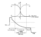
- FIG. 6 is a signal waveform diagram of the pixel unit 10 and signal lines.
- a period during which the auto-zero signal is at a high level shown in FIG. 6 indicates a period during auto-zero (hereinafter referred to as an AZ period).
- the period during which the select transistor SEL is at high level indicates the period during which the select transistor SEL is on.
- the period during which the reset transistor RST is at high level indicates the period during which the reset transistor RST is on.
- the period during which the transfer transistor TG is at high level indicates the period during which the transfer transistor TG is on.
- the signal line VSL indicated by a thick solid line in FIG. 6 indicates the VSL potential at high luminance when there is no excess light.
- a signal line VSL indicated by a dashed line indicates the VSL potential when the PD is irradiated with ultra-high-brightness light and charge exceeding Qs, which is the maximum charge amount that can be accumulated in the photodiode PD, is generated.
- Ramp indicated by a dashed-dotted line indicates a ramp wave signal.
- the offset voltage of the comparator 22 is canceled by applying the P-phase potential to the signal line VSL during the AZ period.
- the P-phase potential may fluctuate.
- the metal light shielding film ML is arranged on the light incident surface side of the pixel section 10, and the light SL is transmitted from the opening provided in the metal light shielding film ML to the photodiode PD. is incident.
- Qs shown in FIG. 5 indicates the maximum charge amount that can be accumulated in the photodiode PD.
- Qfd indicates the maximum charge amount that can be accumulated in the floating diffusion FD.
- FIG. 5 shows the potential in the P phase after the reset operation is finished.
- the floating diffusion FD retains charges generated by charge injection of the reset transistor RST or the like.
- FIG. 5 shows an example in which electrons are held in the floating diffusion as charges.
- the charges exceeding Qfd cross the reset transistor RST, reach the power supply voltage VDD line, and then recombine with holes and disappear. In other words, the amount of charge held in the floating diffusion FD continues to increase until it is scraped off by Qfd.
- FIG. 6 shows the potential fluctuation of the vertical signal line VSL when this change occurs.
- the P-phase potential does not fluctuate, so the AZ process is performed normally at that potential.
- the VSL potential has already dropped and therefore does not change.
- the VSL potential remains the same even when the P-phase transitions to the D-phase.
- the comparator 22 When light with a significantly high amount of light is incident during the AZ period, the comparator 22 performs AZ processing with the P-phase potential whose potential level has decreased.
- FIG. 7 is a diagram illustrating an example of a sunspot countermeasure circuit according to a comparative example.
- FIG. 8 is an explanatory diagram showing operation timings and output waveforms of a sunspot countermeasure circuit according to a comparative example.
- the sunspot countermeasure circuit according to the comparative example includes a clamp circuit 101 provided for each pixel section 10 .
- the clamp circuit 101 includes a P-channel MOS (Metal Oxide Semiconductor) transistor (hereinafter referred to as "PMOS transistor”) MP3 and an N-channel MOS transistor (hereinafter referred to as "NMOS transistor”) MN3.
- PMOS transistor Metal Oxide Semiconductor
- NMOS transistor N-channel MOS transistor
- the PMOS transistor MP3 has a source connected to the power supply, a drain connected to the drain of the NMOS transistor MN3, and a gate to which a predetermined gate voltage XSUNEN is applied.
- the NMOS transistor MN3 has a source connected to the vertical signal line VSL and a gate to which a predetermined threshold voltage Vth3 is applied.
- the clamp circuit 101 sets the gate voltage XSUNEN to low level to turn on the PMOS transistor MP3 during the AZ period.
- the potential of the vertical signal line VSL drops.
- the NMOS transistor MN3 is turned off. After that, when the potential of the vertical signal line VSL drops to the potential defined by the predetermined threshold voltage Vth3, the NMOS transistor MN3 turns on and starts operating.
- the amplification transistor AMP is turned off.
- the clamp circuit 101 clamps the potential of the vertical signal line VSL to the potential defined by the predetermined threshold voltage Vth3.
- the clamp circuit 101 turns off the NMOS transistor MN3 by setting the gate voltage XSUNEN to high level to turn off the PMOS transistor MP3.
- the amplification transistor AMP is turned on, and the potential of the vertical signal line VSL drops as shown in FIG.
- the gate voltage of the transistor MN2 fluctuates according to the fluctuation of the VSL potential after the AZ period.
- a predetermined threshold voltage Vth3 shown in FIG. 7 is set so that the gate voltage of the transistor MN2 is sufficiently low, and set so that the logic inversion of the output value VCO of the comparator 22 does not occur.
- the clamp circuit 101 can suppress the occurrence of sunspots.
- the clamp circuit 101 has the following problems.
- the first problem is that the operation start timing of the NMOS transistor MN3 depends on the gate voltage of the amplification transistor AMP, that is, the potential of the floating diffusion FD (hereinafter referred to as "Vfd") and the threshold voltage Vth3, which is the gate voltage of the NMOS transistor MN3. It occurs when the difference between the amplification transistor AMP and the threshold voltage Vth3.
- FIG. 9 is an explanatory diagram showing changes in current and VSL potential when the clamp circuit 101 according to a comparative example is operated.
- FIG. 9 shows the relationship between the potential difference (Vfd ⁇ Vth3), the current I1 passed by the amplification transistor AMP shown in FIG. 7, the current I2 passed by the NMOS transistor MN3, and the potential fluctuation of the vertical signal line VSL.
- the solid line shows the change in the current I1 accompanying the change in the potential difference (Vfd-Vth3)
- the broken line shows the change in the current I2.
- the lower diagram in FIG. 9 shows the potential fluctuation of the vertical signal line VSL due to the change in the potential difference (Vfd-Vth3).
- the potential of the vertical signal line VSL is represented by the following formula (1).
- the gate-source voltage Vgs(AMP) of the amplification transistor AMP in the equation (1) is expressed by the following equation (2).
- the relationship of the following formula (3) holds among the currents I1, I2, and I3 shown in FIG.
- the current I1 is the drain current of the amplification transistor AMP
- W/L is the aspect ratio of the amplification transistor AMP
- ⁇ n is the carrier mobility
- Cox is the gate capacitance per unit area
- Vth is the threshold voltage of the amplification transistor AMP.
- the amplification transistor AMP and the NMOS transistor MN3 shown in FIG. 7 constitute a differential circuit, and the division ratio of the current I3 changes depending on the potential difference between the gates. Therefore, when the potential difference between the gates becomes smaller, the NMOS transistor MN3 starts to flow the current I2, and the current I1 decreases accordingly (see equation (3)).
- a source follower is configured with the amplification transistor AMP and the NMOS transistor MN4 through which the current I3 flows. Therefore, when the current I1 does not fluctuate, that is, when the gate-source voltage Vgs (AMP) does not fluctuate, the source potential fluctuates according to the fluctuation of the potential Vfd of the floating diffusion FD. be kept.
- the potential that can be used as a source follower is only the range where the potential Vfd of the floating diffusion FD is higher than the point A shown in FIG.
- the potential at which the potential of the vertical signal line VSL is clamped is the point B shown in FIG. 9 at which the potential of the vertical signal line VSL further drops and the amplification transistor AMP is turned off. That is, the potential drop of the vertical signal line VSL to be clamped at point A shown in FIG. 9 stops only at point B, and the output D (dynamic) range of the vertical signal line VSL is narrowed by that potential (first problem). .
- the first problem for example, there is a method of detecting the voltage drop of the vertical signal line VSL using a comparison circuit equivalent to the comparator 22.
- a comparison circuit equivalent to the comparator 22 in order to reduce the dead zone (the range from point A to point B shown in FIG. 9) in the first problem, accuracy equivalent to that of the comparator 22 is required, resulting in a large circuit scale.
- second problem since it is necessary to provide a circuit for detecting the voltage drop of the vertical signal line VSL for each column, there arises a problem that the circuit scale further increases (second problem).
- the clamp level can only be adjusted by the gate-source voltage Vgs of the PMOS transistor.
- the adjustment of the clamp level is difficult because it can be performed only by the aspect ratio of the size of the PMOS transistor MP3 (third problem).
- the clamp circuit 101 shown in FIG. 7 is a circuit that performs a clamp operation when the threshold voltage Vth3 exceeds a drop in the potential Vfd of the floating diffusion FD. .
- the potential Vfd of the floating diffusion FD increases as the amount of excess light increases. Therefore, in the clamp circuit 101, the potential of the vertical signal line VSL cannot be clamped by the NMOS transistor MN3.
- the clamp circuit 101 according to the comparative example cannot be used for Hall sensors (fourth problem).
- FIG. 11 is a circuit diagram showing a first example of the excess light amount detection circuit 1p.
- constituent elements that are the same as the constituent elements shown in FIG. 7 are denoted by the same reference numerals as those shown in FIG. 7, thereby omitting redundant description.
- the excess light amount detection circuit 1p has an NMOS transistor Mn1 and a capacitor Ca, and detects variations in the P-phase potential due to the amount of excess light received, typically sunlight.
- the capacitor Ca may be replaced with a resistor as long as it is a high impedance element.
- the NMOS transistor Mn1 has a source connected to the vertical signal line VSL of the image sensor and a drain connected to one terminal of the capacitor Ca.
- the other terminal of capacitor Ca is connected to the power supply voltage VDD line.
- a predetermined threshold voltage Vth1 is applied to the gate of the NMOS transistor Mn1 through the switch SW1.
- the operation of the excess light amount detection circuit 1p will be described.
- the operation when the reset of the floating diffusion FD is finished and the P-phase potential is held in the floating diffusion FD to enter the AZ period will be described.
- the capacitor Ca is discharged in advance by a circuit (not shown), and the potential at the point P holds the power supply voltage VDD.
- connection node P between the capacitor Ca and the NMOS transistor Mn1 in the excess light amount detection circuit 1p is at the power supply voltage VDD when the reset of the floating diffusion FD is completed, and no charge is stored in the capacitor Ca.
- threshold voltage Vth1 the threshold level defined by the gate voltage of the NMOS transistor Mn1 (hereinafter referred to as threshold voltage Vth1), the NMOS transistor Mn1 is turned off, and the connection node between the capacitor Ca and the NMOS transistor Mn1 is turned off.
- P is the power supply voltage.
- the NMOS transistor Mn1 is turned on, current flows through the capacitor Ca, and charge begins to accumulate. Accordingly, the potential of the connection node P between the capacitor Ca and the NMOS transistor Mn1 is lowered.
- the excess light amount detection circuit 1p when the pixel unit 10 receives an excess amount of light, the potential of the vertical signal line VSL drops to the potential defined by the threshold voltage Vth1.
- the excess light level detection circuit 1p transmits the potential at the connection point P as the detection result of the excess light level from the excess light level detection terminal to the subsequent circuit, thereby notifying that the P-phase potential has changed due to the overlight level. It is possible to disregard the operation and perform the process of converting the video signal of the pixel into white.
- the overlight amount detection circuit 1p connects the gate voltage of the NMOS transistor Mn1 to the ground through the switch SW1, ends detection, and returns to normal operation.
- the excess light amount detection circuit 1p turns off the NMOS transistor Mn1 during the P-phase period and the D-phase period in which the P-phase potential or the D-phase potential is supplied via the vertical signal line VSL. Therefore, in normal operation in which the P-phase potential does not fluctuate, the signal transmission is not affected.
- FIG. 12 is an explanatory diagram showing changes in current and VSL potential when the excess light amount detection circuit 1p is operated.
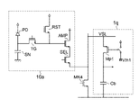
- FIG. 13 is a diagram showing an example of an excess light amount detection circuit 1q for detecting an excess light amount received by a hall sensor.
- a pixel portion 10a of FIG. 13 has a photodiode PD and a capacitor SN connected in series between a power supply voltage node and a ground node. The anode of photodiode PD is connected to the drain of transfer transistor TG.
- the cathode of photodiode PD is connected to the power supply voltage node, and photodiode PD is in a reverse bias state.
- the transfer transistor TG When the transfer transistor TG is turned on, charges (holes) accumulated in the capacitor SN move to the floating diffusion FD, but the capacitor SN and the floating diffusion FD are connected in parallel and capacitively divided. Therefore, the charges (holes) accumulated in the capacitor SN are divided and held by the capacitor SN and the floating diffusion FD.
- FIG. 12 shows the relationship between the potential difference (Vfd-Vth1), the current I1 passed by the amplification transistor AMP shown in FIG. 11, the current I2 passed by the NMOS transistor Mn1, and the potential fluctuation of the vertical signal line VSL.
- logic inversion is performed using only the current at the moment when the NMOS transistor Mn1 starts operating, and then the current is turned off, so linearity deterioration in inversion occurs. do not have.
- the threshold level can be set to the maximum value of the output D range, and a wide output D range can be secured.
- the excess light amount detection circuit 1p can be composed of an NMOS transistor Mn1 and a capacitor Ca. There is almost no difference, and high-precision detection is possible in a wide range.
- the threshold level for clamping the potential of the vertical signal line VSL can be freely adjusted by setting the gate voltage of the NMOS transistor Mn1.
- the sensing element should be a PMOS transistor Mp1 as shown in FIG.
- the excess light detection circuit 1q is composed of a PMOS transistor Mp1 and a capacitor Cb.
- the capacitor Cb may be replaced with a resistor as long as it is a high impedance element.
- the PMOS transistor Mp1 has a source connected to the vertical signal line VSL of the image sensor and a drain connected to one terminal of the capacitor Cb.
- the other terminal of capacitor Cb is connected to the source of NMOS transistor MN4.
- a predetermined threshold voltage Vth1 is applied to the gate of the PMOS transistor Mp1 through the switch SW1.
- the excess light amount detection circuits 1p and 1q detect the amount of excess light received based on the potential fluctuation of the vertical signal line VSL itself. Therefore, the excess light amount detection circuits 1p and 1q can output a signal corresponding to a binary value indicating whether or not an excess amount of light has been received to a subsequent circuit as a detection result of the amount of excess light.
- the excess light amount detection circuits 1p and 1q output to the counter 23 a signal indicating the detection result of the amount of excess light.
- the counter 23 stops counting when a signal indicating the amount of light received is input from the excess light amount detection circuits 1p and 1q.
- the image sensor 100 can prevent the occurrence of sunspots by forcibly whitening pixels in which an excess amount of received light has been detected.
- the excess light amount detection circuits 1p and 1q stop the comparison operation of the comparator 22 by a signal indicating the detection result of the amount of excess light.
- the comparator 22 stops comparing the potential of the vertical signal line VSL and the ramp wave signal when a signal indicating the amount of light received is input from the excess light amount detection circuits 1p and 1q.
- the image sensor 100 can prevent the occurrence of sunspots by forcibly whitening pixels in which an excess amount of received light has been detected.
- the image sensor 100 can prevent the occurrence of sunspots by processing the results detected by the excess light amount detection circuits 1p and 1q in subsequent circuits.
- the overlight amount detection circuits 1p and 1q shown in FIGS. 11 and 13 are sensitive to power supply voltage fluctuations, and the power supply voltage fluctuations may reduce the overlight amount detection accuracy (first problem). . More specifically, when the power supply voltage fluctuates, the voltage level of the threshold voltage Vth1 in the excess light detection circuits 1p and 1q shown in FIGS. 11 and 13 may fluctuate. Since the threshold voltage Vth1 is generated from the power supply voltage, if the power supply voltage fluctuates, the threshold voltage Vth1 may also fluctuate. When the threshold voltage Vth1 fluctuates, the potential level at which the potential of the vertical signal line VSL is clamped fluctuates. In particular, the threshold voltage Vth1 varies depending on the position of the pixel in the pixel array section 2, and there is a possibility that the detection accuracy of the amount of excess light varies from pixel to pixel.
- the threshold voltage Vth1 varies due to the difference in the parasitic resistance, and there is a possibility that the detection accuracy of the amount of excess light may vary from pixel to pixel. (Second problem).
- the threshold voltage of the amplification transistor AMP may vary for each pixel section 10 in the pixel array section 2. Due to the variation in the threshold voltage of the amplification transistor AMP, the potential of the vertical signal line VSL varies, and the amount of excess light varies for each pixel. There is a risk that variations in the detection accuracy of will occur (third problem).
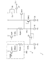
- FIG. 14 is a circuit diagram of the excess light amount detection circuit 1 according to the first improved example.
- the excess light amount detection circuit 1 of FIG. 14 differs in circuit configuration from the excess light amount detection circuit 1p of FIG. Specifically, the excess light amount detection circuit 1 in FIG. 14 includes a dummy circuit 9 in addition to the NMOS transistor Mn1 and the capacitor Ca in FIG.
- the dummy circuit 9 adjusts the gate voltage of the NMOS transistor Mn1 in consideration of at least one of the voltage level fluctuation of the power supply voltage, the parasitic resistance Rpara of the signal line VSL, and the threshold voltage fluctuation of the amplification transistor AMP.
- the dummy circuit 9 has a dummy pixel section 10D and an NMOS transistor (also called a second dummy transistor) DMn2.
- the dummy pixel section 10D is connected to all the pixel sections 10 in the same row in the pixel array section 2, as will be described later.
- a second dummy transistor DMn2 is provided for each corresponding pixel section 10 .
- the dummy pixel section 10D is associated with two or more pixel sections 10 (typically, all pixel sections 10 in the same row) arranged in the first direction (row direction) in the pixel array section 2. be provided.
- a second dummy transistor DMn2 is provided for each NMOS transistor Mn1 in each pixel section 10 .
- one second dummy transistor DMn2 may be provided for two or more NMOS transistors Mn1 in the same row.
- the dummy pixel section 10D has a first dummy transistor DMn1 corresponding to the amplification transistor AMP in the pixel section 10, and a dummy signal line DVSL connected to the first dummy transistor DMn1.
- the first dummy transistor DMn1 has the same size, same conductivity type and same electrical characteristics as the amplification transistor.
- the second dummy transistor DMn2 has the same size, same conductivity type and same electrical characteristics as the corresponding second transistor.
- the dummy pixel section 10D may have a third dummy transistor DMn3 corresponding to the select transistor SEL in the pixel section 10.
- the third dummy transistor DMn3 in the column selected by the row scanning circuit 3 is turned on, and the on/off of the third transistor SEL and the third dummy transistor DMn3 in the same column are synchronized.
- the third dummy transistor DMn3 is connected between the source of the first dummy transistor DMn1 and the dummy signal line DVSL.
- the parasitic resistance Rpara of the dummy signal line DVSL connected to the dummy pixel section 10D is the same as the parasitic resistance Rpara of the signal line VSL connected to the pixel section 10D.
- the gate voltage of the NMOS transistor Mn1 can be adjusted in consideration of the parasitic resistance Rpara of the signal line VSL.
- the first dummy transistor DMn1 in the dummy pixel section 10D simulates the amplification transistor AMP in the pixel section 10, and when the threshold voltage and gate-source voltage of the amplification transistor AMP fluctuate, the first dummy transistor DMn1 The dummy transistor DMn1 also fluctuates in the same way.
- the second dummy transistor DMn2 similarly fluctuates.
- a large number of pixel units 10 are arranged in the row direction and the column direction in the pixel array unit 2, and the parasitic resistance Rpara of the signal line VSL differs depending on the location of the pixel unit 10.
- the electrical characteristics of the amplification transistors AMP in the pixel section 10 are not always the same throughout the pixel array section 2, and variations in electrical characteristics may occur due to manufacturing variations. Therefore, it is desirable to provide the dummy circuit 9 for each row in the pixel array section 2 and connect all the pixel sections 10 in the same row to the same dummy circuit 9 .
- the second dummy transistor DMn2 simulates the NMOS transistor Mn1, and is desirably arranged near the NMOS transistor Mn1. By arranging them close to each other, the electrical characteristics of the second dummy transistor DMn2 can be made similar to the electrical characteristics of the NMOS transistor Mn1.
- FIG. 14 shows the parasitic resistance Rpara on the dummy signal line DVSL and the signal line VSL
- this parasitic resistance Rpara is not a physical resistance element but a general term for wiring resistance components.
- the parasitic resistance of the signal line VSL connected to the pixel section 10 in the same row is approximately the same as that of the signal line VSL.
- Rpara can be provided to the dummy signal line DVSL.
- the dummy signal line DVSL is connected to a current source 12D that flows a current equivalent to that of the current source 12 connected to the signal line VSL.
- a voltage follower circuit 13 is connected to the dummy signal line DVSL.
- the voltage follower circuit 13 has a differential amplifier, the + terminal of this differential amplifier is connected to the dummy signal line DVSL, and the - terminal is connected to the output node of the differential amplifier.
- the output node of the differential amplifier is connected to the source of the second dummy transistor DMn2.
- the voltage follower circuit 13 has a function of separating the impedances of the dummy signal line DVSL and the signal line VSL, and the provision of the voltage follower circuit 13 increases noise immunity.
- the dummy circuit 9 is provided for each row in the pixel array section 2 and is connected to all the pixel sections 10 in the same row. easier. Therefore, by providing the voltage follower circuit 13, the noise of the dummy signal line DVSL is not superimposed on the signal line VSL.
- the second dummy transistor DMn2 is an NMOS transistor whose gate and drain are short-circuited, and the gate of the NMOS transistor Mn1 is connected to this short-circuit path. Thereby, the second dummy transistor DMn2 and the NMOS transistor Mn1 form a current mirror circuit.
- a current source 26 is connected between the source of the second dummy transistor DMn2 and the ground node.
- the signal line VSL connected to the pixel section 10 is connected to the source of the NMOS transistor Mn1, as in FIG.
- the potential of the signal line VSL decreases, and the gate-source voltage of the NMOS transistor Mn1 increases.
- this gate-source voltage exceeds the threshold voltage of the NMOS transistor Mn1
- the NMOS transistor Mn1 is turned on, the drain voltage of the NMOS transistor Mn1 drops, and the voltage is applied to the connection node between the NMOS transistor Mn1 and the capacitor Ca through the buffer 27.
- the connected overcurrent detection terminal becomes low level.
- the gate voltage of the NMOS transistor Mn1 has a voltage value corresponding to the dummy circuit 9 and the second dummy transistor DMn2.
- the gate voltage of the NMOS transistor Mn1 is less susceptible to variations in threshold voltage of the amplification transistor AMP in the pixel section 10, parasitic resistance Rpara of the signal line VSL, and variations in power supply voltage.
- the excess light amount detection circuit 1 in FIG. 14 operates at the same operation timing as in FIG. Capacitor Ca is pre-discharged by switch 28 .
- an excessive amount of light such as sunlight is incident on the photodiode PD during the AZ period
- the potential of the vertical signal line VSL is lowered
- the transistor Mn1 is turned on, current flows through the capacitor Ca, and charge is accumulated. start. Accordingly, the potential of the connection node between the capacitor Ca and the transistor Mn1 is lowered.
- the overlight level detection terminal TL1 changes from high level to low level and the overlight level is detected, the transistor Mn1 is turned off.
- the excess light amount detection circuit 1 When the excess light amount detection circuit 1 does not operate, the switch 28 is closed, the excess light amount detection terminal TL1 is held at a high level, and the potential of the gate signal VSUN of the dummy transistor DMn1 becomes sufficiently low. As a result, the excess light amount detection circuit 1 sufficiently lowers the gate potential of the transistor Mn1 during the P-phase period and the D-phase period in which the P-phase potential or the D-phase potential is supplied via the vertical signal line VSL. Therefore, normal operation during the P-phase period or the D-phase period does not affect the signal transmission.
- the gate signal VSUN of the first dummy transistor DMn1 in the dummy circuit 9 of FIG. 14 is generated by the dummy control circuit 29.
- the dummy control circuit 29 generates a gate signal VSUN for setting the gate of the first dummy transistor DMn1 to an arbitrary potential within the AZ period. More specifically, dummy control circuit 29 generates gate signal VSUN so as not to be affected by fluctuations in the voltage level of the power supply voltage.
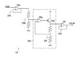
- FIG. 15 is a circuit diagram showing an example of the internal configuration of the dummy control circuit 29.
- the dummy control circuit 29 of FIG. 15 has a first voltage follower circuit 29a, a first resistive voltage dividing circuit 29b, an LDO (Low Drop-Out) circuit 29c, and a second voltage follower circuit 29d.
- the first voltage follower circuit 29a and the second voltage follower circuit 29d have differential amplifiers 29e and 29f that short-circuit the output node and the - terminal, like the voltage follower circuit of FIG.
- a reference voltage Vref is applied to the + terminal of the differential amplifier 29e in the first voltage follower circuit 29a, and the signal VSUN is output from the output node of the differential amplifier 29f in the second voltage follower circuit 29d.
- the signal VSUN is input to the gate of the first dummy transistor DMn1 in the dummy circuit 9 of FIG.
- the signal VSUN is a signal that has an arbitrary potential during the AZ period.
- the LDO circuit 29c has a differential amplifier 29g, a PMOS transistor 29h, and a second resistance voltage dividing circuit 29i.
- the source of the PMOS transistor 29h is connected to the power supply voltage node, and a second resistance voltage dividing circuit 29i is connected between the drain of the PMOS transistor 29h and the ground node.
- a voltage divided by the first resistance voltage dividing circuit 29b is input to the + terminal of the differential amplifier 29g, and a voltage divided by the second resistance voltage dividing circuit 29i is inputted to the ⁇ terminal of the differential amplifier 29g. is entered.
- the LDO circuit 29c of FIG. 15 can keep the drain voltage of the PMOS transistor constant even if the voltage level of the power supply voltage fluctuates. Therefore, the voltage level of the signal VSUN output from the second voltage follower circuit 29d is not affected by fluctuations in the voltage level of the power supply voltage.
- the excess light amount detection circuit 1 in FIG. 14 is a circuit for reading electrons photoelectrically converted by the photodiode as in FIG. 11, it is also possible to configure a circuit for reading holes.
- FIG. 16 is a circuit diagram of the excess light amount detection circuit 1a according to the second improved example, which is a circuit for reading holes photoelectrically converted by the photodiode.
- the same reference numerals are assigned to the components that are common to those of FIG. 14, and the differences will be mainly described below.
- the PMOS transistor Mp1 and the capacitor Cb are connected in series between the signal line VSL and the ground node.
- a connection node between the PMOS transistor Mp1 and the capacitor Cb outputs an excess light amount detection signal through the buffer 27 .
- the second dummy transistor DMp2 is a PMOS transistor whose gate and drain are short-circuited, and the gate of the PMOS transistor Mp1 is connected to this short-circuit path. Thereby, the second dummy transistor DMp2 and the PMOS transistor Mp1 form a current mirror circuit.
- the pixel unit 10 the signal line VSL, and the dummy pixel having the same configuration as the NMOS transistor Mn1 (or PMOS transistor Mp1) that outputs the overlight amount detection signal.
- 10D a dummy signal line DVSL, and a second dummy transistor DMn2 or DMp2. Therefore, fluctuations in the voltage level of the power supply voltage, parasitic resistance Rpara of the signal line VSL, and fluctuations in the threshold voltage of the amplification transistor AMP in the pixel section 10 can be offset. Sunspots can be prevented by detecting this with high accuracy.
- FIG. 17 is a diagram showing an example of the arrangement location of the dummy pixel portion 10D of FIGS. 14 and 16.
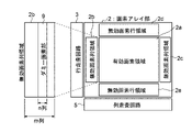
- the pixel array section 2 includes an effective pixel region 2a for outputting effective pixel signals, two ineffective pixel column regions 2b and 2c arranged on both sides of the effective pixel region 2a in the column direction, and a row direction of the effective pixel region 2a. has two invalid pixel row regions 2d and 2e arranged on both sides of the .
- a row scanning circuit 3 is provided on one side or both sides of the pixel array section 2 in the column direction.
- the dummy pixel section 10D in FIGS. 14 and 16 is arranged in one invalid pixel row region 2b. As described above, the dummy pixel section 10D is provided for each row and connected to all the pixel sections 10 in the same row in the column direction. If the number of pixel units 10 in the column direction is large, the dummy pixel unit 10D may be separately provided for each of two or more pixel units 10 in the same row to detect the amount of excess light.
- the second dummy transistor DMn2 is provided for each pixel section 10. Since the second dummy transistor DMn2 has the same electrical characteristics as the NMOS transistor (or PMOS transistor) in the pixel section 10, it is desirable to arrange it near the NMOS transistor (or PMOS transistor).
- the excess light amount detection circuits 1 and 1a in FIGS. 14 and 16 can solve the first to third problems of the excess light amount detection circuits 1p and 1q shown in FIGS. 14 and 16 includes a first dummy transistor DMn1 driven by the same power supply voltage as the amplification transistor AMP in the pixel section 10 and a signal line VSL connected to the pixel section 10. It has a dummy signal line DVSL having a parasitic resistance Rpara about the same as the parasitic resistance Rpara, and a second dummy transistor DMn2 having a threshold voltage about the same as that of the transistors Mn1 and Mp1 connected to the signal line VSL.
- the gate voltages of the transistors Mn1 and Mp1 are generated.
- the amount of excess light can be detected without being affected by fluctuations in the parasitic resistance Rpara of the signal line VSL, fluctuations in the voltage level of the power supply voltage, and fluctuations in the threshold voltages of the transistors Mn1 and Mp1.
- the LDO circuit 29c is used to generate the signal VSUN that supplies an arbitrary potential that defines the sunspot detection level to the gate of the first dummy transistor DMn1 during the AZ period, fluctuations in the voltage level of the power supply voltage are not received. .
- 18 and 19 show a schematic configuration of the light receiving element 110 to which the excess light amount detection circuits 1 and 1a according to the present disclosure are applied.
- 18 shows a planar configuration of the light receiving element 110
- FIG. 19 shows a cross-sectional configuration along line BB' of FIG.
- the light receiving element 110 is applied to, for example, an infrared sensor using a compound semiconductor material such as a III-V group semiconductor. It has a photoelectric conversion function for light with a wavelength of more than 2400 nm).
- the light receiving element 110 is provided with, for example, a plurality of light receiving unit regions P1 (pixels P1) arranged two-dimensionally (FIG. 19).
- the light receiving element 110 has a central element region R1 and a peripheral region R2 provided outside the element region R1 and surrounding the element region R1 (FIG. 18).
- the light receiving element 110 has a conductive film 15B provided from the element region R1 to the peripheral region R2. This conductive film 15B has an opening in a region facing the central portion of the element region R1.
- the light receiving element 110 has a laminated structure in which an element substrate 30 and a readout circuit board 40, which is an example of a circuit board, are laminated (FIG. 19).
- One surface of the element substrate 30 is a light incident surface (light incident surface S1), and the surface opposite to the light incident surface S1 (the other surface) is a bonding surface (bonding surface S2) with the readout circuit board 40. .
- the element substrate 30 has a wiring layer 10W, a first electrode 31, a semiconductor layer 10S (first semiconductor layer), a second electrode 15 and a passivation film 16 in this order from a position near the readout circuit board 40.
- the surface of the semiconductor layer 10 ⁇ /b>S facing the wiring layer 10 ⁇ /b>W and the end surface (side surface) are covered with an insulating film 17 .
- the readout circuit board 40 is a so-called ROIC (Readout integrate circuit). 30 and a semiconductor substrate 35 facing the semiconductor substrate 30 .
- the element substrate 30 has a semiconductor layer 10S in the element region R1.
- the region provided with the semiconductor layer 10S is the element region R1 of the light receiving element 110.
- a region of the element region R1 exposed from the conductive film 15B (a region facing the opening of the conductive film 15B) is a light receiving region.
- a region of the element region R1 covered with the conductive film 15B is an OPB (Optical Black) region R1B.
- the OPB region R1B is provided so as to surround the light receiving region.
- the OPB region R1B is used to obtain a black level pixel signal.
- the element substrate 30 has the buried layer 18 together with the insulating film 17 in the peripheral region R2.
- Holes H1 and H2 that penetrate the element substrate 30 and reach the readout circuit substrate 40 are provided in the peripheral region R2.
- the light receiving element 110 light enters the semiconductor layer 10S from the light incident surface S1 of the element substrate 30 via the passivation film 16, the second electrode 15 and the second contact layer .
- Signal charges photoelectrically converted in the semiconductor layer 10S move through the first electrode 31 and the wiring layer 10W and are read out by the readout circuit board 40.
- FIG. The configuration of each part will be described below.
- the wiring layer 10W is provided over the element region R1 and the peripheral region R2, and has a bonding surface S2 with the readout circuit board 40.
- the bonding surface S2 of the element substrate 30 is provided in the element region R1 and the peripheral region R2.
- the bonding surface S2 of the element region R1 and the bonding surface S2 of the peripheral region R2 form the same plane.
- the bonding surface S2 of the peripheral region R2 is formed by providing the embedded layer 18. As shown in FIG.
- the wiring layer 10W has contact electrodes 19E and dummy electrodes 19ED in, for example, the interlayer insulating films 19A and 19B.
- the interlayer insulating film 19B is arranged on the readout circuit board 40 side, the interlayer insulating film 19A is arranged on the first contact layer 32 side, and these interlayer insulating films 19A and 19B are provided in a laminated manner.
- the interlayer insulating films 19A and 19B are made of, for example, an inorganic insulating material. Examples of inorganic insulating materials include silicon nitride (SiN), aluminum oxide (Al2O3), silicon oxide (SiO2) and hafnium oxide (HfO2).
- the interlayer insulating films 19A and 19B may be made of the same inorganic insulating material.
- the contact electrode 19E is provided, for example, in the element region R1.
- the contact electrode 19E is for electrically connecting the first electrode 31 and the readout circuit board 40, and is provided for each pixel P1 in the element region R1.
- Adjacent contact electrodes 19E are electrically separated by buried layer 18 and interlayer insulating films 19A and 19B.
- the contact electrode 19E is composed of, for example, a copper (Cu) pad, and is exposed on the joint surface S2.
- the dummy electrode 19ED is provided, for example, in the peripheral region R2. This dummy electrode 19ED is connected to a dummy electrode 22ED of a wiring layer 20W, which will be described later.
- the dummy electrode 19ED is formed, for example, in the same process as the contact electrode 19E.
- the dummy electrode 19ED is composed of, for example, a copper (Cu) pad and exposed to the joint surface S2.
- the first electrode 31 provided between the contact electrode 19E and the semiconductor layer 10S receives signal charges (holes or electrons, hereinafter for the sake of convenience, signal charges generated in the photoelectric conversion layer 33 are assumed to be holes) generated in the photoelectric conversion layer 33. , and is provided for each pixel P1 in the element region R1.
- the first electrode 31 is provided so as to fill the opening of the insulating film 17, and is in contact with the semiconductor layer 10S (more specifically, a diffusion region 32A described later).
- the first electrode 31 is, for example, larger than the opening of the insulating film 17 and part of the first electrode 31 is provided in the embedded layer 18 .
- the upper surface (the surface on the semiconductor layer 10S side) of the first electrode 31 is in contact with the diffusion region 32A, and the lower surface and part of the side surface of the first electrode 31 are in contact with the buried layer 18 .
- Adjacent first electrodes 31 are electrically separated by the insulating film 17 and the embedded layer 18 .
- the first electrode 31 is, for example, titanium (Ti), tungsten (W), titanium nitride (TiN), platinum (Pt), gold (Au), germanium (Ge), palladium (Pd), zinc (Zn), nickel (Ni) and aluminum (Al), or an alloy containing at least one of them.
- the first electrode 31 may be a single film of such constituent materials, or may be a laminated film in which two or more kinds are combined.
- the first electrode 31 is composed of a laminated film of titanium and tungsten.
- the thickness of the first electrode 31 is, for example, several ten nm to several hundred nm.
- the semiconductor layer 10S includes, for example, a first contact layer 32, a photoelectric conversion layer 33 and a second contact layer 34 in order from the wiring layer 10W.
- the first contact layer 32, the photoelectric conversion layer 33, and the second contact layer 34 have the same planar shape, and their end surfaces are arranged at the same positions in plan view.
- the first contact layer 32 is provided, for example, in common for all pixels P1 and arranged between the insulating film 17 and the photoelectric conversion layer 33 .
- the first contact layer 32 is for electrically separating adjacent pixels P1, and is provided with, for example, a plurality of diffusion regions 32A.
- a compound semiconductor material having a bandgap larger than that of the compound semiconductor material forming the photoelectric conversion layer 33 for the first contact layer 32 dark current can be suppressed.
- n-type InP indium phosphide
- the diffusion regions 32A provided in the first contact layer 32 are arranged apart from each other.
- the diffusion region 32A is arranged for each pixel P1, and the first electrode 31 is connected to each diffusion region 32A.
- a diffusion region 32A is also provided in the OPB region R1B.
- the diffusion region 32A is for reading signal charges generated in the photoelectric conversion layer 33 for each pixel P1, and contains p-type impurities, for example. Examples of p-type impurities include Zn (zinc).
- a pn junction interface is formed between the diffusion region 32A and the first contact layer 32 other than the diffusion region 32A, and the adjacent pixels P1 are electrically isolated.
- the diffusion region 32A is provided, for example, in the thickness direction of the first contact layer 32 and is also provided in a part of the photoelectric conversion layer 33 in the thickness direction.
- the photoelectric conversion layer 33 Between the first electrode 31 and the second electrode 15, more specifically, the photoelectric conversion layer 33 between the first contact layer 32 and the second contact layer 34 is common to all the pixels P1, for example. is provided.
- the photoelectric conversion layer 33 absorbs light of a predetermined wavelength to generate signal charges, and is made of a compound semiconductor material such as an i-type III-V group semiconductor.
- Compound semiconductor materials constituting the photoelectric conversion layer 33 include, for example, InGaAs (indium gallium arsenide), InAsSb (indium arsenide antimony), InAs (indium arsenide), InSb (indium antimonide), and HgCdTe (mercury cadmium tellurium). mentioned.
- the photoelectric conversion layer 33 may be made of Ge (germanium). In the photoelectric conversion layer 33, for example, photoelectric conversion of light with wavelengths from the visible region to the short infrared region is performed.
- the second contact layer 34 is provided, for example, in common for all the pixels P1.
- the second contact layer 34 is provided between the photoelectric conversion layer 33 and the second electrode 15 and is in contact with them.
- the second contact layer 34 is a region where charges discharged from the second electrode 15 move, and is made of, for example, a compound semiconductor containing n-type impurities.
- n-type InP indium phosphide
- the second electrode 15 is provided on the second contact layer 34 (light incident side) so as to be in contact with the second contact layer 34, for example, as an electrode common to each pixel P1.
- the second electrode 15 is for discharging the charge that is not used as the signal charge among the charges generated in the photoelectric conversion layer 33 (cathode). For example, if holes are read from the first electrode 31 as signal charges, electrons, for example, can be ejected through this second electrode 15 .
- the second electrode 15 is made of a conductive film that can transmit incident light such as infrared rays.
- ITO Indium Tin Oxide
- ITiO In2O3--TiO2
- the second electrode 15 may be provided in a grid pattern, for example, so as to partition adjacent pixels P1. A conductive material with low light transmittance can be used for the second electrode 15 .
- the passivation film 16 covers the second electrode 15 from the light incident surface S1 side.
- the passivation film 16 may have an antireflection function. Silicon nitride (SiN), aluminum oxide (Al2O3), silicon oxide (SiO2), tantalum oxide (Ta2O3), and the like can be used for the passivation film 16, for example.
- the passivation film 16 has an opening 16H in the OPB region R1B.
- the opening 16H is provided, for example, in a frame shape surrounding the light receiving area (FIG. 1q).
- the opening 16H may be, for example, a rectangular or circular hole in plan view.
- the conductive film 15B is electrically connected to the second electrode 15 through the opening 16H of the passivation film 16. As shown in FIG.
- the insulating film 17 is provided between the first contact layer 32 and the embedded layer 18 , and the end face of the first contact layer 32 , the end face of the photoelectric conversion layer 33 , the end face of the second contact layer 34 and the second electrode 15 . , and is in contact with the passivation film 16 in the peripheral region R2.
- This insulating film 17 is composed of an oxide such as silicon oxide (SiOx) or aluminum oxide (Al2O3).
- the insulating film 17 may be configured with a laminated structure composed of a plurality of films.
- the insulating film 17 may be made of a silicon (Si)-based insulating material such as silicon oxynitride (SiON), carbon-containing silicon oxide (SiOC), silicon nitride (SiN), and silicon carbide (SiC).
- Si silicon
- SiON silicon oxynitride
- SiOC carbon-containing silicon oxide
- SiN silicon nitride
- SiC silicon carbide
- the thickness of the insulating film 17 is, for example, several ten nm to several hundred nm.
- the conductive film 15B is provided from the OPB region R1B to the hole H1 in the peripheral region R2.
- the conductive film 15B is in contact with the second electrode 15 through the opening 16H of the passivation film 16 provided in the OPB region R1B, and is in contact with the wiring (wiring 22CB described later) of the readout circuit board 20 through the hole H1.
- a voltage is supplied from the readout circuit board 40 to the second electrode 15 via the conductive film 15B.
- the conductive film 15B functions as a voltage supply path to such a second electrode 15 and also functions as a light shielding film, forming the OPB region R1B.
- the conductive film 15B is made of a metal material containing, for example, tungsten (W), aluminum (Al), titanium (Ti), molybdenum (Mo), tantalum (Ta), or copper (Cu).
- a passivation film may be provided on the conductive film 15B.
- An adhesive layer B may be provided between the end of the second contact layer 34 and the second electrode 15 .
- the adhesive layer B is used when forming the light receiving element 110, and serves to bond the semiconductor layer 10S to the temporary substrate.
- the adhesive layer B is composed of, for example, tetraethoxysilane (TEOS) or silicon oxide (SiO2).
- TEOS tetraethoxysilane
- SiO2 silicon oxide
- the adhesive layer B is provided, for example, wider than the end surface of the semiconductor layer 10S, and is covered with the embedded layer 18 together with the semiconductor layer 10S.
- An insulating film 17 is provided between the adhesive layer B and the embedded layer 18 .
- the excess light amount detection circuits 1 and 1a are provided on the readout circuit board 40 when applied to the light receiving element 110 . As a result, the excess light amount detection circuits 1 and 1a can detect the amount of excess light received by the image sensor with high accuracy without increasing the circuit scale of the light receiving element 110 .
- FIG. 20 is a cross-sectional view showing a pixel structure to which the excess light detection circuits 1 and 1a according to the present disclosure are applied.
- An element substrate is provided on the upper side, which is the light incident side, of the semiconductor substrate 60, which is an example of a circuit substrate.
- An N-type semiconductor thin film 41 serving as a photoelectric conversion portion is formed on the element substrate over the entire surface of the pixel array region.
- InGaP, InAlP, InGaAs, InAlAs, or a compound semiconductor having a chalcopyrite structure is used for the N-type semiconductor thin film 41.
- a compound semiconductor with a chalcopyrite structure is a material that provides a high light absorption coefficient and high sensitivity over a wide wavelength range, and is preferably used as the N-type semiconductor thin film 41 for photoelectric conversion.
- Such chalcopyrite structure compound semiconductors are composed of elements surrounding IV group elements such as Cu, Al, Ga, In, S, and Se, and are A mixed crystal etc. are illustrated.
- amorphous silicon (Si), germanium (Ge), quantum dot photoelectric conversion films, organic photoelectric conversion films, and the like can also be used as the material of the N-type semiconductor thin film 41.
- an InGaAs compound semiconductor is used as the N-type semiconductor thin film 41 .
- a high-concentration P-type layer 42 constituting a pixel electrode is formed for each pixel on the lower side of the N-type semiconductor thin film 41 on the semiconductor substrate 60 side.
- an N-type layer 43 as a pixel separation region for separating each pixel is formed of a compound semiconductor such as InP, for example.
- This N-type layer 43 has a role of preventing dark current in addition to functioning as a pixel separation region.
- an N-type layer 44 having a higher concentration than the N-type semiconductor thin film 41 is also formed on the upper side of the N-type semiconductor thin film 41, which is the light incident side, using a compound semiconductor such as InP used as a pixel separation region. It is This high-concentration N-type layer 44 functions as a barrier layer that prevents backflow of charges generated in the N-type semiconductor thin film 41 .
- Compound semiconductors such as InGaAs, InP, and InAlAs can be used as the material of the high-concentration N-type layer 44, for example.
- An antireflection film 45 is formed on the high-concentration N-type layer 44 as a barrier layer.
- Examples of materials for the antireflection film 45 include silicon nitride (SiN), hafnium oxide (HfO2), aluminum oxide (Al2O3), zirconium oxide (ZrO2), tantalum oxide (Ta2Ta5), and titanium oxide (TiO2). can be done.
- Either the high-concentration N-type layer 44 or the antireflection film 45 also functions as an upper electrode of the electrodes sandwiching the N-type semiconductor thin film 41 from above and below.
- a predetermined voltage Va is applied to the layer 44 or the antireflection film 45 .
- a color filter 46 and an on-chip lens 47 are further formed on the antireflection film 45 .
- the color filter 46 is a filter that transmits light (wavelength light) of any one of R (red), G (green), and B (blue). ing.
- a passivation layer 51 and an insulating layer 52 are formed below the high-concentration P-type layer 42 constituting the pixel electrode and the N-type layer 43 as the pixel separation region.
- the connection electrodes 53A and 53B and the bump electrode 54 are formed so as to penetrate the passivation layer 51 and the insulating layer 52 .
- the connection electrodes 53A and 53B and the bump electrode 54 electrically connect the high-concentration P-type layer 42 forming the pixel electrode and the capacitive element for storing charge.
- the excess light amount detection circuits 1 and 1a When applied to the pixel structure shown in FIG. 20, the excess light amount detection circuits 1 and 1a are provided on a semiconductor substrate 60, which is an example of a circuit substrate. As a result, the excess light amount detection circuits 1 and 1a can detect the amount of excess light received by the image sensor with high accuracy without increasing the circuit scale of the pixel structure shown in FIG.
- Excess light detection circuits 1 and 1a according to the present disclosure can be applied to various products.
- the technology according to the present disclosure can be applied to any type of movement such as automobiles, electric vehicles, hybrid electric vehicles, motorcycles, bicycles, personal mobility, airplanes, drones, ships, robots, construction machinery, agricultural machinery (tractors), etc. It may also be implemented as a body-mounted device.
- FIG. 21 is a block diagram showing a schematic configuration example of a vehicle control system 7000, which is an example of a mobile control system to which the technology according to the present disclosure can be applied.
- Vehicle control system 7000 comprises a plurality of electronic control units connected via communication network 7010 .
- the vehicle control system 7000 includes a drive system control unit 7100, a body system control unit 7200, a battery control unit 7300, an outside information detection unit 7400, an inside information detection unit 7500, and an integrated control unit 7600.
- the communication network 7010 connecting these multiple control units conforms to any standard such as CAN (Controller Area Network), LIN (Local Interconnect Network), LAN (Local Area Network) or FlexRay (registered trademark). It may be an in-vehicle communication network.
- Each control unit includes a microcomputer that performs arithmetic processing according to various programs, a storage unit that stores programs executed by the microcomputer or parameters used in various calculations, and a drive circuit that drives various devices to be controlled. Prepare.
- Each control unit has a network I/F for communicating with other control units via a communication network 7010, and communicates with devices or sensors inside and outside the vehicle by wired communication or wireless communication. A communication I/F for communication is provided. In FIG.
- the functional configuration of the integrated control unit 7600 includes a microcomputer 7610, a general-purpose communication I/F 7620, a dedicated communication I/F 7630, a positioning unit 7640, a beacon receiving unit 7650, an in-vehicle equipment I/F 7660, an audio image output unit 7670, An in-vehicle network I/F 7680 and a storage unit 7690 are shown.
- Other control units are similarly provided with microcomputers, communication I/Fs, storage units, and the like.
- the drive system control unit 7100 controls the operation of devices related to the drive system of the vehicle according to various programs.
- the driving system control unit 7100 includes a driving force generator for generating driving force of the vehicle such as an internal combustion engine or a driving motor, a driving force transmission mechanism for transmitting the driving force to the wheels, and a steering angle of the vehicle. It functions as a control device such as a steering mechanism to adjust and a brake device to generate braking force of the vehicle.
- the drive system control unit 7100 may have a function as a control device such as ABS (Antilock Brake System) or ESC (Electronic Stability Control).
- a vehicle state detection section 7110 is connected to the drive system control unit 7100 .
- the vehicle state detection unit 7110 includes, for example, a gyro sensor that detects the angular velocity of the axial rotational motion of the vehicle body, an acceleration sensor that detects the acceleration of the vehicle, an accelerator pedal operation amount, a brake pedal operation amount, and a steering wheel steering. At least one of sensors for detecting angle, engine speed or wheel rotation speed is included.
- Drive system control unit 7100 performs arithmetic processing using signals input from vehicle state detection unit 7110, and controls the internal combustion engine, drive motor, electric power steering device, brake device, and the like.
- the body system control unit 7200 controls the operation of various devices equipped on the vehicle body according to various programs.
- the body system control unit 7200 functions as a keyless entry system, a smart key system, a power window device, or a control device for various lamps such as headlamps, back lamps, brake lamps, winkers or fog lamps.
- body system control unit 7200 can receive radio waves transmitted from a portable device that substitutes for a key or signals from various switches.
- Body system control unit 7200 receives the input of these radio waves or signals and controls the door lock device, power window device, lamps, etc. of the vehicle.
- the battery control unit 7300 controls the secondary battery 7310, which is the power supply source for the driving motor, according to various programs. For example, the battery control unit 7300 receives information such as battery temperature, battery output voltage, or remaining battery capacity from a battery device including a secondary battery 7310 . The battery control unit 7300 performs arithmetic processing using these signals, and performs temperature adjustment control of the secondary battery 7310 or control of a cooling device provided in the battery device.
- the vehicle exterior information detection unit 7400 detects information outside the vehicle in which the vehicle control system 7000 is installed.
- the imaging section 7410 and the vehicle exterior information detection section 7420 is connected to the vehicle exterior information detection unit 7400 .
- the imaging unit 7410 includes at least one of a ToF (Time Of Flight) camera, a stereo camera, a monocular camera, an infrared camera, and other cameras.
- the vehicle exterior information detection unit 7420 includes, for example, an environment sensor for detecting the current weather or weather, or a sensor for detecting other vehicles, obstacles, pedestrians, etc. around the vehicle equipped with the vehicle control system 7000. ambient information detection sensor.
- the environmental sensor may be, for example, at least one of a raindrop sensor that detects rainy weather, a fog sensor that detects fog, a sunshine sensor that detects the degree of sunshine, and a snow sensor that detects snowfall.
- the ambient information detection sensor may be at least one of an ultrasonic sensor, a radar device, and a LIDAR (Light Detection and Ranging, Laser Imaging Detection and Ranging) device.
- LIDAR Light Detection and Ranging, Laser Imaging Detection and Ranging
- These imaging unit 7410 and vehicle exterior information detection unit 7420 may be provided as independent sensors or devices, or may be provided as a device in which a plurality of sensors or devices are integrated.
- FIG. 22 shows an example of the installation positions of the imaging unit 7410 and the vehicle exterior information detection unit 7420.
- the imaging units 7910 , 7912 , 7914 , 7916 , and 7918 are provided, for example, at least one of the front nose, side mirrors, rear bumper, back door, and windshield of the vehicle 7900 .
- An image pickup unit 7910 provided in the front nose and an image pickup unit 7918 provided above the windshield in the vehicle interior mainly acquire an image in front of the vehicle 7900 .
- Imaging units 7912 and 7914 provided in the side mirrors mainly acquire side images of the vehicle 7900 .
- An imaging unit 7916 provided in the rear bumper or back door mainly acquires an image behind the vehicle 7900 .
- An imaging unit 7918 provided above the windshield in the passenger compartment is mainly used for detecting preceding vehicles, pedestrians, obstacles, traffic lights, traffic signs, lanes, and the like.
- FIG. 22 shows an example of the imaging range of each of the imaging units 7910, 7912, 7914, and 7916.
- the imaging range a indicates the imaging range of the imaging unit 7910 provided in the front nose
- the imaging ranges b and c indicate the imaging ranges of the imaging units 7912 and 7914 provided in the side mirrors, respectively
- the imaging range d is The imaging range of an imaging unit 7916 provided on the rear bumper or back door is shown. For example, by superimposing the image data captured by the imaging units 7910, 7912, 7914, and 7916, a bird's-eye view image of the vehicle 7900 viewed from above can be obtained.
- the vehicle exterior information detectors 7920, 7922, 7924, 7926, 7928, and 7930 provided on the front, rear, sides, corners, and above the windshield of the vehicle interior of the vehicle 7900 may be, for example, ultrasonic sensors or radar devices.
- the exterior information detectors 7920, 7926, and 7930 provided above the front nose, rear bumper, back door, and windshield of the vehicle 7900 may be LIDAR devices, for example.
- These vehicle exterior information detection units 7920 to 7930 are mainly used to detect preceding vehicles, pedestrians, obstacles, and the like.
- the vehicle exterior information detection unit 7400 causes the imaging section 7410 to capture an image of the exterior of the vehicle, and receives the captured image data.
- the vehicle exterior information detection unit 7400 also receives detection information from the vehicle exterior information detection unit 7420 connected thereto.
- the vehicle exterior information detection unit 7420 is an ultrasonic sensor, radar device, or LIDAR device
- the vehicle exterior information detection unit 7400 emits ultrasonic waves, electromagnetic waves, or the like, and receives reflected wave information.
- the vehicle exterior information detection unit 7400 may perform object detection processing or distance detection processing such as people, vehicles, obstacles, signs, or characters on the road surface based on the received information.
- the vehicle exterior information detection unit 7400 may perform environment recognition processing for recognizing rainfall, fog, road surface conditions, etc., based on the received information.
- the vehicle exterior information detection unit 7400 may calculate the distance to the vehicle exterior object based on the received information.
- the vehicle exterior information detection unit 7400 may perform image recognition processing or distance detection processing for recognizing people, vehicles, obstacles, signs, characters on the road surface, etc., based on the received image data.
- the vehicle exterior information detection unit 7400 performs processing such as distortion correction or alignment on the received image data, and synthesizes image data captured by different imaging units 7410 to generate a bird's-eye view image or a panoramic image. good too.
- the vehicle exterior information detection unit 7400 may perform viewpoint conversion processing using image data captured by different imaging units 7410 .
- the in-vehicle information detection unit 7500 detects in-vehicle information.
- the in-vehicle information detection unit 7500 is connected to, for example, a driver state detection section 7510 that detects the state of the driver.
- the driver state detection unit 7510 may include a camera that captures an image of the driver, a biosensor that detects the biometric information of the driver, a microphone that collects sounds in the vehicle interior, or the like.
- a biosensor is provided, for example, on a seat surface, a steering wheel, or the like, and detects biometric information of a passenger sitting on a seat or a driver holding a steering wheel.
- the in-vehicle information detection unit 7500 may calculate the degree of fatigue or concentration of the driver based on the detection information input from the driver state detection unit 7510, and determine whether the driver is dozing off. You may The in-vehicle information detection unit 7500 may perform processing such as noise canceling processing on the collected sound signal.
- the integrated control unit 7600 controls overall operations within the vehicle control system 7000 according to various programs.
- An input section 7800 is connected to the integrated control unit 7600 .
- the input unit 7800 is realized by a device that can be input-operated by the passenger, such as a touch panel, button, microphone, switch or lever.
- the integrated control unit 7600 may be input with data obtained by recognizing voice input by a microphone.
- the input unit 7800 may be, for example, a remote control device using infrared rays or other radio waves, or may be an externally connected device such as a mobile phone or PDA (Personal Digital Assistant) corresponding to the operation of the vehicle control system 7000.
- PDA Personal Digital Assistant
- the input unit 7800 may be, for example, a camera, in which case the passenger can input information through gestures.
- the input section 7800 may include an input control circuit that generates an input signal based on information input by the passenger or the like using the input section 7800 and outputs the signal to the integrated control unit 7600, for example.
- a passenger or the like operates the input unit 7800 to input various data to the vehicle control system 7000 and instruct processing operations.
- the storage unit 7690 may include a ROM (Read Only Memory) that stores various programs executed by the microcomputer, and a RAM (Random Access Memory) that stores various parameters, calculation results, sensor values, and the like.
- the storage section 7690 may be realized by a magnetic storage device such as a HDD (Hard Disc Drive), a semiconductor storage device, an optical storage device, a magneto-optical storage device, or the like.
- the general-purpose communication I/F 7620 is a general-purpose communication I/F that mediates communication between various devices existing in the external environment 7750.
- General-purpose communication I / F7620 is a cellular communication protocol such as GSM (registered trademark) (Global System of Mobile communications), WiMAX (registered trademark), LTE (registered trademark) (Long Term Evolution) or LTE-A (LTE-Advanced) , or other wireless communication protocols such as wireless LAN (also referred to as Wi-Fi®), Bluetooth®, and the like.
- General-purpose communication I / F 7620 for example, via a base station or access point, external network (e.g., Internet, cloud network or operator-specific network) equipment (e.g., application server or control server) connected to You may
- external network e.g., Internet, cloud network or operator-specific network
- equipment e.g., application server or control server
- the general-purpose communication I / F 7620 uses, for example, P2P (Peer To Peer) technology, terminals that exist near the vehicle (for example, terminals of drivers, pedestrians or stores, or MTC (Machine Type Communication) terminals) may be connected with P2P (Peer To Peer) technology
- terminals that exist near the vehicle for example, terminals of drivers, pedestrians or stores, or MTC (Machine Type Communication) terminals
- MTC Machine Type Communication
- the dedicated communication I/F 7630 is a communication I/F that supports a communication protocol designed for use in vehicles.
- Dedicated communication I / F7630 for example, WAVE (Wireless Access in Vehicle Environment), which is a combination of lower layer IEEE802.11p and upper layer IEEE1609, DSRC (Dedicated Short Range Communications), or a standard protocol such as a cellular communication protocol May be implemented.
- the dedicated communication I/F 7630 is typically used for vehicle-to-vehicle communication, vehicle-to-infrastructure communication, vehicle-to-home communication, and vehicle-to-pedestrian communication. ) perform V2X communication, which is a concept involving one or more of the communications.
- the positioning unit 7640 receives GNSS signals from GNSS (Global Navigation Satellite System) satellites (for example, GPS signals from GPS (Global Positioning System) satellites) to perform positioning, and obtains the latitude, longitude, and altitude of the vehicle. Generate location information containing Note that the positioning unit 7640 may specify the current position by exchanging signals with a wireless access point, or may acquire position information from a terminal such as a mobile phone, PHS, or smart phone having a positioning function.
- GNSS Global Navigation Satellite System
- GPS Global Positioning System
- the beacon receiving unit 7650 receives, for example, radio waves or electromagnetic waves transmitted from wireless stations installed on the road, and acquires information such as the current position, traffic jams, road closures, or required time. Note that the function of the beacon reception unit 7650 may be included in the dedicated communication I/F 7630 described above.
- the in-vehicle device I/F 7660 is a communication interface that mediates connections between the microcomputer 7610 and various in-vehicle devices 7760 present in the vehicle.
- the in-vehicle device I/F 7660 may establish a wireless connection using a wireless communication protocol such as wireless LAN, Bluetooth (registered trademark), NFC (Near Field Communication), or WUSB (Wireless USB).
- a wireless communication protocol such as wireless LAN, Bluetooth (registered trademark), NFC (Near Field Communication), or WUSB (Wireless USB).
- the in-vehicle device I/F 7660 is connected via a connection terminal (and cable if necessary) not shown, USB (Universal Serial Bus), HDMI (registered trademark) (High-Definition Multimedia Interface, or MHL (Mobile High -definition Link), etc.
- In-vehicle equipment 7760 includes, for example, at least one of a mobile device or wearable device possessed by a passenger, or information equipment carried or attached to the vehicle. In-vehicle equipment 7760 may also include a navigation device that searches for a route to an arbitrary destination. or exchange data signals.
- the in-vehicle network I/F 7680 is an interface that mediates communication between the microcomputer 7610 and the communication network 7010. In-vehicle network I/F 7680 transmits and receives signals and the like according to a predetermined protocol supported by communication network 7010 .
- the microcomputer 7610 of the integrated control unit 7600 uses at least one of a general-purpose communication I/F 7620, a dedicated communication I/F 7630, a positioning unit 7640, a beacon receiving unit 7650, an in-vehicle device I/F 7660, and an in-vehicle network I/F 7680.
- the vehicle control system 7000 is controlled according to various programs on the basis of the information acquired by. For example, the microcomputer 7610 calculates control target values for the driving force generator, steering mechanism, or braking device based on acquired information on the inside and outside of the vehicle, and outputs a control command to the drive system control unit 7100. good too.
- the microcomputer 7610 realizes ADAS (Advanced Driver Assistance System) functions including collision avoidance or shock mitigation, follow-up driving based on inter-vehicle distance, vehicle speed maintenance driving, vehicle collision warning, or vehicle lane departure warning. Cooperative control may be performed for the purpose of In addition, the microcomputer 7610 controls the driving force generator, the steering mechanism, the braking device, etc. based on the acquired information about the surroundings of the vehicle, thereby autonomously traveling without depending on the operation of the driver. Cooperative control may be performed for the purpose of driving or the like.
- ADAS Advanced Driver Assistance System
- Microcomputer 7610 receives information obtained through at least one of general-purpose communication I/F 7620, dedicated communication I/F 7630, positioning unit 7640, beacon receiving unit 7650, in-vehicle device I/F 7660, and in-vehicle network I/F 7680. Based on this, three-dimensional distance information between the vehicle and surrounding objects such as structures and people may be generated, and local map information including the surrounding information of the current position of the vehicle may be created. Further, based on the acquired information, the microcomputer 7610 may predict dangers such as vehicle collisions, pedestrians approaching or entering closed roads, and generate warning signals.
- the warning signal may be, for example, a signal for generating a warning sound or lighting a warning lamp.
- the audio/image output unit 7670 transmits at least one of audio and/or image output signals to an output device capable of visually or audibly notifying the passengers of the vehicle or the outside of the vehicle.
- an audio speaker 7710, a display section 7720, and an instrument panel 7730 are illustrated as output devices.
- Display 7720 may include, for example, at least one of an on-board display and a head-up display.
- the display unit 7720 may have an AR (Augmented Reality) display function.
- the output device may be headphones, a wearable device such as an eyeglass-type display worn by a passenger, or other devices such as a projector or a lamp.
- the display device displays the results obtained by various processes performed by the microcomputer 7610 or information received from other control units in various formats such as text, images, tables, and graphs. Display visually.
- the voice output device converts an audio signal including reproduced voice data or acoustic data into an analog signal and outputs the analog signal audibly.
- At least two control units connected via the communication network 7010 may be integrated as one control unit.
- an individual control unit may be composed of multiple control units.
- vehicle control system 7000 may comprise other control units not shown.
- some or all of the functions that any control unit has may be provided to another control unit. In other words, as long as information is transmitted and received via the communication network 7010, the predetermined arithmetic processing may be performed by any one of the control units.
- sensors or devices connected to any control unit may be connected to other control units, and multiple control units may send and receive detection information to and from each other via communication network 7010. .
- this technique can take the following structures. (1) a pixel unit having a photoelectric conversion element and a first transistor that outputs a signal photoelectrically converted by the photoelectric conversion element to a signal line; and an excess light amount detection circuit that detects that the photoelectric conversion element has received an excess amount of light,
- the excess light amount detection circuit is a second transistor and a capacitor connected in series between the signal line and a reference potential node; a dummy circuit that adjusts the gate voltage of the second transistor in consideration of at least one of fluctuations in the voltage level of the power supply voltage, the parasitic resistance of the signal line, and variations in the threshold voltage of the first transistor.
- imaging device is a pixel unit having a photoelectric conversion element and a first transistor that outputs a signal photoelectrically converted by the photoelectric conversion element to a signal line; and an excess light amount detection circuit that detects that the photoelectric conversion element has received an excess amount of light.
- the dummy circuit a dummy pixel section having a first dummy transistor corresponding to the first transistor and a dummy signal line connected to the first dummy transistor; and a second dummy transistor that controls the gate voltage of the second transistor according to the potential of the dummy signal line.
- the gate voltage of the second transistor is controlled such that the parasitic resistance of the signal line and the parasitic capacitance of the dummy signal line are equal.
- the second dummy transistor and the second transistor constitute a current mirror circuit.
- the first dummy transistor has the same size, the same conductivity type, and the same electrical characteristics as the first transistor;
- the imaging device according to any one of (2) to (4), wherein the second dummy transistor has the same size, the same conductivity type, and the same electrical characteristics as the second transistor.
- a pixel array section having a plurality of the pixel sections arranged in a first direction and a second direction that intersect with each other; The dummy pixel section is provided in association with two or more of the pixel sections arranged in the first direction in the pixel array section, (3) or (4), wherein the second dummy transistor is separately provided for each of the two or more second transistors corresponding to the two or more pixel units arranged in the first direction; The imaging device described.
- the dummy pixel section is provided in association with the two or more second transistors arranged in the same row in the second direction and in the first direction;
- the imaging device according to (6), wherein the second dummy transistor is separately provided for each of the two or more second transistors arranged in the same row in the second direction and in the first direction. .
- the imaging device according to (6) or (7), wherein the second dummy transistor is arranged near the corresponding second transistor.
- the pixel array section has an effective pixel area and two ineffective pixel areas arranged on both sides of the effective pixel area in the first direction;
- (11) The imaging device according to any one of (2) to (10), including a voltage follower circuit connected between the dummy signal line and the second dummy transistor.
- the pixel section has a third transistor connected between the first transistor and the signal line for switching whether to output the signal amplified by the first transistor to the signal line;
- the dummy circuit has a third dummy transistor corresponding to the third transistor;
- the imaging device according to any one of (2) to (11), wherein the third dummy transistor is connected between the first dummy transistor and the dummy signal line.
- a differential amplifier for detecting a potential difference between a voltage signal corresponding to the potential of the signal line and a ramp wave signal whose voltage level changes with time;
- the pixel unit has a floating diffusion that accumulates charges photoelectrically converted by the photoelectric conversion element, and a fourth transistor that resets the charges held in the floating diffusion, After the first period for detecting the offset voltage of the differential amplifier, the potential difference between the voltage signal corresponding to the potential of the signal line in a state where the charge of the floating diffusion is reset and the ramp wave signal is detected by the differential amplifier. A second period is provided for detection at According to (13), the excess light amount detection circuit outputs a signal indicating that the photoelectric conversion element has received an excess amount of light from a connection node of the second transistor and the capacitor during the second period. imaging device.
- the imaging device further comprising a dummy control circuit that supplies an arbitrary potential that defines a solar cell detection level to the gate of the first dummy transistor during the first period.
- the dummy control circuit has an LDO (Low DropOut) circuit that generates the gate signal so as not to be affected by fluctuations in the voltage level of the power supply voltage.
- the pixel unit outputs a signal corresponding to the electrons photoelectrically converted by the photoelectric conversion element to the signal line,
- the imaging device according to any one of (2) to (16), wherein both the second transistor and the second dummy transistor are N-type MOS transistors.
- the pixel unit outputs to the signal line a signal corresponding to the holes photoelectrically converted by the photoelectric conversion element,
- the imaging device according to any one of (2) to (16), wherein both the second transistor and the second dummy transistor are P-type MOS transistors.
- a connection node between the second transistor and the capacitor outputs a signal indicating that the photoelectric conversion element has received an excessive amount of light. imaging device.
- an imaging device that outputs a photoelectrically converted imaging signal
- An electronic device comprising a signal processing unit that performs signal processing on the imaging signal
- the imaging device is a pixel unit having a photoelectric conversion element and a first transistor that outputs a signal photoelectrically converted by the photoelectric conversion element to a signal line; and an excess light amount detection circuit that detects that the photoelectric conversion element has received an excess amount of light
- the excess light amount detection circuit is a second transistor and a capacitor connected in series between the signal line and a reference potential node; a dummy circuit that adjusts the gate voltage of the second transistor in consideration of at least one of fluctuations in the voltage level of the power supply voltage, the parasitic resistance of the signal line, and variations in the threshold voltage of the first transistor. ,Electronics.
Landscapes
- Engineering & Computer Science (AREA)
- Multimedia (AREA)
- Signal Processing (AREA)
- Transforming Light Signals Into Electric Signals (AREA)
- Solid State Image Pick-Up Elements (AREA)
Abstract
Description
前記光電変換素子が過光量の光を受光したことを検知する過光量検知回路と、を備え、
前記過光量検知回路は、
前記信号線と基準電位ノードとの間に直列に接続される第2トランジスタ及びキャパシタと、
電源電圧の電圧レベルの変動、前記信号線の寄生抵抗、及び前記第1トランジスタの閾値電圧のばらつきの少なくとも一つを考慮に入れて前記第2トランジスタのゲート電圧を調整するダミー回路と、を有する、撮像装置が提供される。
前記第1トランジスタに対応する第1のダミートランジスタと、前記第1のダミートランジスタに接続されるダミー信号線と、を有するダミー画素部と、
前記ダミー信号線の電位に応じて前記第2トランジスタのゲート電圧を制御する第2のダミートランジスタと、を有してもよい。
前記第2のダミートランジスタは、前記第2トランジスタと同一のサイズ、同一の導電型及び同一の電気特性を有してもよい。
前記ダミー画素部は、前記画素アレイ部内の前記第1方向に配置される2以上の前記画素部に対応づけて設けられ、
前記第2のダミートランジスタは、前記第1方向に配置される前記2以上の画素部に対応する2以上の前記第2トランジスタのそれぞれに対して別個に設けられてもよい。
前記第2のダミートランジスタは、前記第2方向の同一行、かつ前記第1方向に配置される前記2以上の第2トランジスタのそれぞれに対して別個に設けられてもよい。
前記ダミー画素部は、前記2つの無効画素領域の一方に配置されてもよい。
前記ダミー回路は、前記第3トランジスタに対応する第3のダミートランジスタを有し、
前記第3のダミートランジスタは、前記第1のダミートランジスタと前記ダミー信号線との間に接続されてもよい。
前記第1のダミートランジスタは、前記差動増幅器のオフセット電圧を調整する期間内にオンしてもよい。
前記差動増幅器のオフセット電圧を検出する第1期間の後に、前記フローティングディフュージョンの電荷をリセットした状態での前記信号線の電位に応じた電圧信号と前記ランプ波信号との電位差を前記差動増幅器にて検出する第2期間が設けられ、
前記過光量検知回路は、前記第2期間に、前記第2トランジスタ及び前記キャパシタの接続ノードから、前記光電変換素子が過光量の光を受光したことを示す信号を出力してもよい。
前記第2トランジスタ及び前記第2のダミートランジスタはいずれも、N型のMOSトランジスタであってもよい。
前記第2トランジスタ及び前記第2のダミートランジスタはいずれも、P型のMOSトランジスタであってもよい。
前記撮像信号に対する信号処理を行う信号処理部と、を備える電子機器であって、
前記撮像装置は、
光電変換素子と、前記光電変換素子で光電変換された信号を信号線に出力する第1トランジスタと、を有する画素部と、
前記光電変換素子が過光量の光を受光したことを検知する過光量検知回路と、を備え、
前記過光量検知回路は、
前記信号線と基準電位ノードとの間に直列に接続される第2トランジスタ及びキャパシタと、
電源電圧の電圧レベルの変動、前記信号線の寄生抵抗、及び前記第1トランジスタの閾値電圧のばらつきの少なくとも一つを考慮に入れて前記第2トランジスタのゲート電圧を調整するダミー回路と、を有する、電子機器が提供される。
次に、AD変換回路11の構成および動作について説明する。図3はAD変換回路11の内部構成を示す回路図である。AD変換回路には、カラム方向に延びる垂直信号線VSLごとに、コンパレータ22とカウンタ23とが設けられる。各コンパレータ22には、参照信号生成回路8で生成されたランプ波信号が供給される。カウンタ23は、タイミング制御回路7からのクロック信号に同期して、カウントアップ又はカウントダウン動作を行う。
次に、コンパレータ22の回路構成および動作について説明する。図4はコンパレータ22の回路構成の一例を示す説明図である。
次に、図5および図6を参照して、撮像装置100の課題となる現象について説明する。図5は、画素部10の断面図と、過光量受光時における画素部10のポテンシャル図である。図6は、画素部10及び信号線の信号波形図である。
次に、図7および図8を参照して、太陽黒点の発生を抑制する一比較例に係る太陽黒点対策回路について説明する。図7は、一比較例に係る太陽黒点対策回路の一例を示す図である。図8は、一比較例に係る太陽黒点対策回路の動作タイミングと出力波形とを示す説明図である。



そこで、上記した第1~第4の課題を解決し、回路規模を増大させず、出力Dレンジを狭めることなく、イメージセンサによる過光量の受光を高精度に検知できる過光量検知回路1を備えた撮像装置100について検討する。
次に、図12および図13を参照して、上記した第1~第4の課題について検討する。図12は、過光量検知回路1pを動作させた場合の電流とVSL電位の変化を示す説明図である。図13は、ホールセンサによる過光量の受光を検知する過光量検知回路1qの一例を示す図である。図13の画素部10aは、電源電圧ノードと接地ノードの間に直列に接続されるフォトダイオードPD及びキャパシタSNを有する。フォトダイオードPDのアノードが転送トランジスタTGのドレインに接続されている。フォトダイオードPDのカソードは電源電圧ノードに接続されており、フォトダイオードPDは逆バイアス状態である。転送トランジスタTGがオンすると、キャパシタSNに蓄積された電荷(正孔)がフローティングディフュージョンFDに移動するが、キャパシタSNとフローティングディフュージョンFDは並列接続であり、容量分割される。よって、キャパシタSNに蓄積された電荷(正孔)は、キャパシタSNとフローティングディフュージョンFDに分割されて保持される。
図11と図13に示す過光量検知回路1p、1qは、電源電圧の変動に対して敏感であり、電源電圧の変動により、過光量の検知精度が低下するおそれがある(第1の課題)。より詳細には、電源電圧が変動すると、図11と図13の過光量検知回路1p、1q内の閾値電圧Vth1の電圧レベルが変動するおそれがある。閾値電圧Vth1は、電源電圧から生成されるため、電源電圧が変動すると、閾値電圧Vth1も変動するおそれがある。閾値電圧Vth1が変動すると、垂直信号線VSLの電位をクランプさせる電位レベルが変動する。特に、画素アレイ部2内の画素位置により、閾値電圧Vth1が変動し、画素ごとに過光量の検知精度にばらつきが生じるおそれがある。
図14は第1改善例に係る過光量検知回路1の回路図である。図14の過光量検知回路1は、図11の過光量検知回路1pとは回路構成が異なっている。具体的には、図14の過光量検知回路1は、図11のNMOSトランジスタMn1及びキャパシタCaを備える他に、ダミー回路9を備えている。
次に、図18および図19を参照して本開示に係る過光量検知回路1,1aが適用される受光素子について説明する。図18,図19は、本開示に係る過光量検知回路1,1aが適用される受光素子110の模式的な構成を表したものである。図18は、受光素子110の平面構成を表し、図19は、図18のB-B’線に沿った断面構成を表している。
本開示に係る過光量検知回路1,1aは、様々な製品へ応用することができる。例えば、本開示に係る技術は、自動車、電気自動車、ハイブリッド電気自動車、自動二輪車、自転車、パーソナルモビリティ、飛行機、ドローン、船舶、ロボット、建設機械、農業機械(トラクター)などのいずれかの種類の移動体に搭載される装置として実現されてもよい。
(1)光電変換素子と、前記光電変換素子で光電変換された信号を信号線に出力する第1トランジスタと、を有する画素部と、
前記光電変換素子が過光量の光を受光したことを検知する過光量検知回路と、を備え、
前記過光量検知回路は、
前記信号線と基準電位ノードとの間に直列に接続される第2トランジスタ及びキャパシタと、
電源電圧の電圧レベルの変動、前記信号線の寄生抵抗、及び前記第1トランジスタの閾値電圧のばらつきの少なくとも一つを考慮に入れて前記第2トランジスタのゲート電圧を調整するダミー回路と、を有する、撮像装置。
(2)前記ダミー回路は、
前記第1トランジスタに対応する第1のダミートランジスタと、前記第1のダミートランジスタに接続されるダミー信号線と、を有するダミー画素部と、
前記ダミー信号線の電位に応じて前記第2トランジスタのゲート電圧を制御する第2のダミートランジスタと、を有する、(1)に記載の撮像装置。
(3)前記信号線の寄生抵抗と前記ダミー信号線の寄生容量とが等しくなるように、前記第2トランジスタのゲート電圧が制御される、(2)に記載の撮像装置。
(4)前記第2のダミートランジスタ及び前記第2トランジスタは、カレントミラー回路を構成する、(2)又は(3)に記載の撮像装置。
(5)前記第1のダミートランジスタは、前記第1トランジスタと同一のサイズ、同一の導電型及び同一の電気特性を有し、
前記第2のダミートランジスタは、前記第2トランジスタと同一のサイズ、同一の導電型及び同一の電気特性を有する、(2)乃至(4)のいずれか一項に記載の撮像装置。
(6)互いに交差する第1方向及び第2方向に配置される複数の前記画素部を有する画素アレイ部を備え、
前記ダミー画素部は、前記画素アレイ部内の前記第1方向に配置される2以上の前記画素部に対応づけて設けられ、
前記第2のダミートランジスタは、前記第1方向に配置される前記2以上の画素部に対応する2以上の前記第2トランジスタのそれぞれに対して別個に設けられる、(3)又は(4)に記載の撮像装置。
(7)前記ダミー画素部は、前記第2方向の同一行、かつ前記第1方向に配置される前記2以上の第2トランジスタに対応づけて設けられ、
前記第2のダミートランジスタは、前記第2方向の同一行、かつ前記第1方向に配置される前記2以上の第2トランジスタのそれぞれに対して別個に設けられる、(6)に記載の撮像装置。
(8)前記第2のダミートランジスタは、対応する前記第2トランジスタの近傍に配置される、(6)又は(7)に記載の撮像装置。
(9)前記ダミー画素部は、前記画素アレイ部における前記第1方向の一端側に配置される、(6)乃至(8)のいずれか一項に記載の撮像装置。
(10)前記画素アレイ部は、有効画素領域と、前記有効画素領域の前記第1方向の両側に配置される2つの無効画素領域とを有し、
前記ダミー画素部は、前記2つの無効画素領域の一方に配置される、(9)に記載の撮像装置。
(11)前記ダミー信号線と前記第2のダミートランジスタとの間に接続されるボルテージフォロワ回路を備える、(2)乃至(10)のいずれか一項に記載の撮像装置。
(12)前記画素部は、前記第1トランジスタと前記信号線との間に接続され、前記第1トランジスタで増幅した信号を前記信号線に出力するか否かを切り替える第3トランジスタを有し、
前記ダミー回路は、前記第3トランジスタに対応する第3のダミートランジスタを有し、
前記第3のダミートランジスタは、前記第1のダミートランジスタと前記ダミー信号線との間に接続される、(2)乃至(11)のいずれか一項に記載の撮像装置。
(13)前記信号線の電位に応じた電圧信号と、時間に応じて電圧レベルが変化するランプ波信号との電位差を検出する差動増幅器を備え、
前記第1のダミートランジスタは、前記差動増幅器のオフセット電圧を調整する期間内にオンする、(2)乃至(12)のいずれか一項に記載の撮像装置。
(14)前記画素部は、前記光電変換素子で光電変換された電荷を蓄積するフローティングディフュージョンと、前記フローティングディフュージョンに保持された電荷をリセットする第4トランジスタと、を有し、
前記差動増幅器のオフセット電圧を検出する第1期間の後に、前記フローティングディフュージョンの電荷をリセットした状態での前記信号線の電位に応じた電圧信号と前記ランプ波信号との電位差を前記差動増幅器にて検出する第2期間が設けられ、
前記過光量検知回路は、前記第2期間に、前記第2トランジスタ及び前記キャパシタの接続ノードから、前記光電変換素子が過光量の光を受光したことを示す信号を出力する、(13)に記載の撮像装置。
(15)前記第1期間内に、前記第1のダミートランジスタのゲートに太陽電池検知レベルを規定する任意の電位を供給するダミー制御回路を備える、(14)に記載の撮像装置。
(16)前記ダミー制御回路は、電源電圧の電圧レベルの変動に影響されないように前記ゲートの信号を生成するLDO(Low DropOut)回路を有する、(15)に記載の撮像装置。
(17)前記画素部は、前記光電変換素子で光電変換された電子に応じた信号を前記信号線に出力し、
前記第2トランジスタ及び前記第2のダミートランジスタはいずれも、N型のMOSトランジスタである、(2)乃至(16)のいずれか一項に記載の撮像装置。
(18)前記画素部は、前記光電変換素子で光電変換された正孔に応じた信号を前記信号線に出力し、
前記第2トランジスタ及び前記第2のダミートランジスタはいずれも、P型のMOSトランジスタである、(2)乃至(16)のいずれか一項に記載の撮像装置。
(19)前記第2トランジスタ及び前記キャパシタの接続ノードから、前記光電変換素子が過光量の光を受光したことを示す信号が出力される、(1)乃至(18)のいずれか一項に記載の撮像装置。
(20)光電変換された撮像信号を出力する撮像装置と、
前記撮像信号に対する信号処理を行う信号処理部と、を備える電子機器であって、
前記撮像装置は、
光電変換素子と、前記光電変換素子で光電変換された信号を信号線に出力する第1トランジスタと、を有する画素部と、
前記光電変換素子が過光量の光を受光したことを検知する過光量検知回路と、を備え、
前記過光量検知回路は、
前記信号線と基準電位ノードとの間に直列に接続される第2トランジスタ及びキャパシタと、
電源電圧の電圧レベルの変動、前記信号線の寄生抵抗、及び前記第1トランジスタの閾値電圧のばらつきの少なくとも一つを考慮に入れて前記第2トランジスタのゲート電圧を調整するダミー回路と、を有する、電子機器。
Claims (20)
- 光電変換素子と、前記光電変換素子で光電変換された信号を信号線に出力する第1トランジスタと、を有する画素部と、
前記光電変換素子が過光量の光を受光したことを検知する過光量検知回路と、を備え、
前記過光量検知回路は、
前記信号線と基準電位ノードとの間に直列に接続される第2トランジスタ及びキャパシタと、
電源電圧の電圧レベルの変動、前記信号線の寄生抵抗、及び前記第1トランジスタの閾値電圧のばらつきの少なくとも一つを考慮に入れて前記第2トランジスタのゲート電圧を調整するダミー回路と、を有する、撮像装置。 - 前記ダミー回路は、
前記第1トランジスタに対応する第1のダミートランジスタと、前記第1のダミートランジスタに接続されるダミー信号線と、を有するダミー画素部と、
前記ダミー信号線の電位に応じて前記第2トランジスタのゲート電圧を制御する第2のダミートランジスタと、を有する、請求項1に記載の撮像装置。 - 前記信号線の寄生抵抗と前記ダミー信号線の寄生容量とが等しくなるように、前記第2トランジスタのゲート電圧が制御される、請求項2に記載の撮像装置。
- 前記第2のダミートランジスタ及び前記第2トランジスタは、カレントミラー回路を構成する、請求項2に記載の撮像装置。
- 前記第1のダミートランジスタは、前記第1トランジスタと同一のサイズ、同一の導電型及び同一の電気特性を有し、
前記第2のダミートランジスタは、前記第2トランジスタと同一のサイズ、同一の導電型及び同一の電気特性を有する、請求項2に記載の撮像装置。 - 互いに交差する第1方向及び第2方向に配置される複数の前記画素部を有する画素アレイ部を備え、
前記ダミー画素部は、前記画素アレイ部内の前記第1方向に配置される2以上の前記画素部に対応づけて設けられ、
前記第2のダミートランジスタは、前記第1方向に配置される前記2以上の画素部に対応する2以上の前記第2トランジスタのそれぞれに対して別個に設けられる、請求項3に記載の撮像装置。 - 前記ダミー画素部は、前記第2方向の同一行、かつ前記第1方向に配置される前記2以上の第2トランジスタに対応づけて設けられ、
前記第2のダミートランジスタは、前記第2方向の同一行、かつ前記第1方向に配置される前記2以上の第2トランジスタのそれぞれに対して別個に設けられる、請求項6に記載の撮像装置。 - 前記第2のダミートランジスタは、対応する前記第2トランジスタの近傍に配置される、請求項6に記載の撮像装置。
- 前記ダミー画素部は、前記画素アレイ部における前記第1方向の一端側に配置される、請求項6に記載の撮像装置。
- 前記画素アレイ部は、有効画素領域と、前記有効画素領域の前記第1方向の両側に配置される2つの無効画素領域とを有し、
前記ダミー画素部は、前記2つの無効画素領域の一方に配置される、請求項9に記載の撮像装置。 - 前記ダミー信号線と前記第2のダミートランジスタとの間に接続されるボルテージフォロワ回路を備える、請求項2に記載の撮像装置。
- 前記画素部は、前記第1トランジスタと前記信号線との間に接続され、前記第1トランジスタで増幅した信号を前記信号線に出力するか否かを切り替える第3トランジスタを有し、
前記ダミー回路は、前記第3トランジスタに対応する第3のダミートランジスタを有し、
前記第3のダミートランジスタは、前記第1のダミートランジスタと前記ダミー信号線との間に接続される、請求項2に記載の撮像装置。 - 前記信号線の電位に応じた電圧信号と、時間に応じて電圧レベルが変化するランプ波信号との電位差を検出する差動増幅器を備え、
前記第1のダミートランジスタは、前記差動増幅器のオフセット電圧を調整する期間内にオンする、請求項2に記載の撮像装置。 - 前記画素部は、前記光電変換素子で光電変換された電荷を蓄積するフローティングディフュージョンと、前記フローティングディフュージョンに保持された電荷をリセットする第4トランジスタと、を有し、
前記差動増幅器のオフセット電圧を検出する第1期間の後に、前記フローティングディフュージョンの電荷をリセットした状態での前記信号線の電位に応じた電圧信号と前記ランプ波信号との電位差を前記差動増幅器にて検出する第2期間が設けられ、
前記過光量検知回路は、前記第2期間に、前記第2トランジスタ及び前記キャパシタの接続ノードから、前記光電変換素子が過光量の光を受光したことを示す信号を出力する、請求項13に記載の撮像装置。 - 前記第1期間内に、前記第1のダミートランジスタのゲートに太陽黒点検知レベルを規定する任意の電位を供給するダミー制御回路を備える、請求項14に記載の撮像装置。
- 前記ダミー制御回路は、電源電圧の電圧レベルの変動に影響されないように前記ゲートの信号を生成するLDO(Low DropOut)回路を有する、請求項15に記載の撮像装置。
- 前記画素部は、前記光電変換素子で光電変換された電子に応じた信号を前記信号線に出力し、
前記第2トランジスタ及び前記第2のダミートランジスタはいずれも、N型のMOSトランジスタである、請求項2に記載の撮像装置。 - 前記画素部は、前記光電変換素子で光電変換された正孔に応じた信号を前記信号線に出力し、
前記第2トランジスタ及び前記第2のダミートランジスタはいずれも、P型のMOSトランジスタである、請求項2に記載の撮像装置。 - 前記第2トランジスタ及び前記キャパシタの接続ノードから、前記光電変換素子が過光量の光を受光したことを示す信号が出力される、請求項1に記載の撮像装置。
- 光電変換された撮像信号を出力する撮像装置と、
前記撮像信号に対する信号処理を行う信号処理部と、を備える電子機器であって、
前記撮像装置は、
光電変換素子と、前記光電変換素子で光電変換された信号を信号線に出力する第1トランジスタと、を有する画素部と、
前記光電変換素子が過光量の光を受光したことを検知する過光量検知回路と、を備え、
前記過光量検知回路は、
前記信号線と基準電位ノードとの間に直列に接続される第2トランジスタ及びキャパシタと、
電源電圧の電圧レベルの変動、前記信号線の寄生抵抗、及び前記第1トランジスタの閾値電圧のばらつきの少なくとも一つを考慮に入れて前記第2トランジスタのゲート電圧を調整するダミー回路と、を有する、電子機器。
Priority Applications (1)
| Application Number | Priority Date | Filing Date | Title |
|---|---|---|---|
| US18/554,602 US12418733B2 (en) | 2021-04-16 | 2022-03-29 | Imaging apparatus and electronic device |
Applications Claiming Priority (2)
| Application Number | Priority Date | Filing Date | Title |
|---|---|---|---|
| JP2021-069909 | 2021-04-16 | ||
| JP2021069909A JP2022164425A (ja) | 2021-04-16 | 2021-04-16 | 撮像装置及び電子機器 |
Publications (1)
| Publication Number | Publication Date |
|---|---|
| WO2022220095A1 true WO2022220095A1 (ja) | 2022-10-20 |
Family
ID=83640614
Family Applications (1)
| Application Number | Title | Priority Date | Filing Date |
|---|---|---|---|
| PCT/JP2022/015266 Ceased WO2022220095A1 (ja) | 2021-04-16 | 2022-03-29 | 撮像装置及び電子機器 |
Country Status (3)
| Country | Link |
|---|---|
| US (1) | US12418733B2 (ja) |
| JP (1) | JP2022164425A (ja) |
| WO (1) | WO2022220095A1 (ja) |
Families Citing this family (2)
| Publication number | Priority date | Publication date | Assignee | Title |
|---|---|---|---|---|
| US12069391B2 (en) * | 2021-07-29 | 2024-08-20 | Omnivision Technologies, Inc. | Readout architectures for dark current reduction in indirect time-of-flight sensors |
| WO2026042723A1 (ja) * | 2024-08-20 | 2026-02-26 | ソニーセミコンダクタソリューションズ株式会社 | 電子機器、固体撮像装置及び制御方法 |
Citations (2)
| Publication number | Priority date | Publication date | Assignee | Title |
|---|---|---|---|---|
| JP2007036916A (ja) * | 2005-07-29 | 2007-02-08 | Sony Corp | 固体撮像装置、固体撮像装置の駆動方法および撮像装置 |
| JP2008283557A (ja) * | 2007-05-11 | 2008-11-20 | Sony Corp | 固体撮像装置、撮像装置 |
Family Cites Families (1)
| Publication number | Priority date | Publication date | Assignee | Title |
|---|---|---|---|---|
| WO2017130728A1 (ja) * | 2016-01-29 | 2017-08-03 | ソニー株式会社 | 固体撮像装置および電子機器 |
-
2021
- 2021-04-16 JP JP2021069909A patent/JP2022164425A/ja active Pending
-
2022
- 2022-03-29 US US18/554,602 patent/US12418733B2/en active Active
- 2022-03-29 WO PCT/JP2022/015266 patent/WO2022220095A1/ja not_active Ceased
Patent Citations (2)
| Publication number | Priority date | Publication date | Assignee | Title |
|---|---|---|---|---|
| JP2007036916A (ja) * | 2005-07-29 | 2007-02-08 | Sony Corp | 固体撮像装置、固体撮像装置の駆動方法および撮像装置 |
| JP2008283557A (ja) * | 2007-05-11 | 2008-11-20 | Sony Corp | 固体撮像装置、撮像装置 |
Also Published As
| Publication number | Publication date |
|---|---|
| US20240205559A1 (en) | 2024-06-20 |
| JP2022164425A (ja) | 2022-10-27 |
| US12418733B2 (en) | 2025-09-16 |
Similar Documents
| Publication | Publication Date | Title |
|---|---|---|
| US11863911B2 (en) | Imaging system, method of controlling imaging system, and object recognition system | |
| CN111164965B (zh) | 固态摄像器件和电子设备 | |
| US12131552B2 (en) | Imaging system, method for controlling imaging system, and object recognition system | |
| US12262131B2 (en) | Imaging device and imaging method | |
| US12309515B2 (en) | Imaging device and imaging method | |
| US11659300B2 (en) | Solid-state image sensor, method of driving solid-state image sensor, and electronic apparatus | |
| US11418750B2 (en) | Imaging element and electronic device | |
| CN113647089B (zh) | 成像系统 | |
| JP7659508B2 (ja) | 撮像装置、電子機器及び撮像方法 | |
| CN112840183A (zh) | 光检测装置、光检测装置的控制方法和测距装置 | |
| CN115699791A (zh) | 成像装置和成像方法 | |
| US12418733B2 (en) | Imaging apparatus and electronic device | |
| WO2020153055A1 (ja) | デジタル-アナログ変換装置、撮像装置、及び、電子機器 | |
| US20230247323A1 (en) | Imaging device and imaging method | |
| WO2022196459A1 (ja) | 光電変換素子及び撮像装置 | |
| US20250350859A1 (en) | Solid-state imaging device | |
| US20250358538A1 (en) | Solid-state imaging element and imaging device | |
| US20250343999A1 (en) | Solid-state image-capturing device, and image-capturing apparatus | |
| WO2025004582A1 (ja) | 故障検知装置、固体撮像装置および故障検知方法 | |
| WO2022186040A1 (ja) | 撮像装置、その駆動方法、および電子機器 | |
| WO2025052881A1 (ja) | 固体撮像装置及び電子機器 | |
| US20240080587A1 (en) | Solid-state imaging device and electronic instrument | |
| WO2024106169A1 (ja) | 光検出素子及び電子機器 | |
| WO2026018431A1 (ja) | 撮像素子、及び撮像装置 | |
| WO2024122394A1 (ja) | 光検出素子及び電子機器 |
Legal Events
| Date | Code | Title | Description |
|---|---|---|---|
| 121 | Ep: the epo has been informed by wipo that ep was designated in this application |
Ref document number: 22788020 Country of ref document: EP Kind code of ref document: A1 |
|
| WWE | Wipo information: entry into national phase |
Ref document number: 18554602 Country of ref document: US |
|
| NENP | Non-entry into the national phase |
Ref country code: DE |
|
| 122 | Ep: pct application non-entry in european phase |
Ref document number: 22788020 Country of ref document: EP Kind code of ref document: A1 |
|
| WWG | Wipo information: grant in national office |
Ref document number: 18554602 Country of ref document: US |