WO2022215663A1 - Silica glass member and method for producing same - Google Patents
Silica glass member and method for producing same Download PDFInfo
- Publication number
- WO2022215663A1 WO2022215663A1 PCT/JP2022/016901 JP2022016901W WO2022215663A1 WO 2022215663 A1 WO2022215663 A1 WO 2022215663A1 JP 2022016901 W JP2022016901 W JP 2022016901W WO 2022215663 A1 WO2022215663 A1 WO 2022215663A1
- Authority
- WO
- WIPO (PCT)
- Prior art keywords
- silica glass
- glass member
- bubbles
- member according
- surface area
- Prior art date
Links
- VYPSYNLAJGMNEJ-UHFFFAOYSA-N Silicium dioxide Chemical compound O=[Si]=O VYPSYNLAJGMNEJ-UHFFFAOYSA-N 0.000 title claims abstract description 127
- 238000004519 manufacturing process Methods 0.000 title claims description 15
- 238000004438 BET method Methods 0.000 claims abstract description 6
- 239000011261 inert gas Substances 0.000 claims description 12
- 239000004071 soot Substances 0.000 claims description 12
- PXHVJJICTQNCMI-UHFFFAOYSA-N Nickel Chemical compound [Ni] PXHVJJICTQNCMI-UHFFFAOYSA-N 0.000 claims description 10
- 238000012545 processing Methods 0.000 claims description 10
- 239000011575 calcium Substances 0.000 claims description 7
- 239000011651 chromium Substances 0.000 claims description 7
- 239000010949 copper Substances 0.000 claims description 7
- 239000011777 magnesium Substances 0.000 claims description 7
- 239000011572 manganese Substances 0.000 claims description 7
- 239000011734 sodium Substances 0.000 claims description 7
- 239000010936 titanium Substances 0.000 claims description 7
- 238000010438 heat treatment Methods 0.000 claims description 6
- XEEYBQQBJWHFJM-UHFFFAOYSA-N Iron Chemical compound [Fe] XEEYBQQBJWHFJM-UHFFFAOYSA-N 0.000 claims description 4
- 229910052793 cadmium Inorganic materials 0.000 claims description 4
- 229910052804 chromium Inorganic materials 0.000 claims description 4
- 229910052802 copper Inorganic materials 0.000 claims description 4
- 239000012535 impurity Substances 0.000 claims description 4
- 229910052744 lithium Inorganic materials 0.000 claims description 4
- 229910052749 magnesium Inorganic materials 0.000 claims description 4
- 229910052748 manganese Inorganic materials 0.000 claims description 4
- 229910052751 metal Inorganic materials 0.000 claims description 4
- 239000002184 metal Substances 0.000 claims description 4
- 229910052759 nickel Inorganic materials 0.000 claims description 4
- 229910052700 potassium Inorganic materials 0.000 claims description 4
- 239000004065 semiconductor Substances 0.000 claims description 4
- 150000003377 silicon compounds Chemical class 0.000 claims description 4
- 229910052709 silver Inorganic materials 0.000 claims description 4
- 229910052719 titanium Inorganic materials 0.000 claims description 4
- OYPRJOBELJOOCE-UHFFFAOYSA-N Calcium Chemical compound [Ca] OYPRJOBELJOOCE-UHFFFAOYSA-N 0.000 claims description 3
- 229910052684 Cerium Inorganic materials 0.000 claims description 3
- VYZAMTAEIAYCRO-UHFFFAOYSA-N Chromium Chemical compound [Cr] VYZAMTAEIAYCRO-UHFFFAOYSA-N 0.000 claims description 3
- RYGMFSIKBFXOCR-UHFFFAOYSA-N Copper Chemical compound [Cu] RYGMFSIKBFXOCR-UHFFFAOYSA-N 0.000 claims description 3
- DGAQECJNVWCQMB-PUAWFVPOSA-M Ilexoside XXIX Chemical compound C[C@@H]1CC[C@@]2(CC[C@@]3(C(=CC[C@H]4[C@]3(CC[C@@H]5[C@@]4(CC[C@@H](C5(C)C)OS(=O)(=O)[O-])C)C)[C@@H]2[C@]1(C)O)C)C(=O)O[C@H]6[C@@H]([C@H]([C@@H]([C@H](O6)CO)O)O)O.[Na+] DGAQECJNVWCQMB-PUAWFVPOSA-M 0.000 claims description 3
- WHXSMMKQMYFTQS-UHFFFAOYSA-N Lithium Chemical compound [Li] WHXSMMKQMYFTQS-UHFFFAOYSA-N 0.000 claims description 3
- FYYHWMGAXLPEAU-UHFFFAOYSA-N Magnesium Chemical compound [Mg] FYYHWMGAXLPEAU-UHFFFAOYSA-N 0.000 claims description 3
- PWHULOQIROXLJO-UHFFFAOYSA-N Manganese Chemical compound [Mn] PWHULOQIROXLJO-UHFFFAOYSA-N 0.000 claims description 3
- ZLMJMSJWJFRBEC-UHFFFAOYSA-N Potassium Chemical compound [K] ZLMJMSJWJFRBEC-UHFFFAOYSA-N 0.000 claims description 3
- BQCADISMDOOEFD-UHFFFAOYSA-N Silver Chemical compound [Ag] BQCADISMDOOEFD-UHFFFAOYSA-N 0.000 claims description 3
- RTAQQCXQSZGOHL-UHFFFAOYSA-N Titanium Chemical compound [Ti] RTAQQCXQSZGOHL-UHFFFAOYSA-N 0.000 claims description 3
- 229910052782 aluminium Inorganic materials 0.000 claims description 3
- XAGFODPZIPBFFR-UHFFFAOYSA-N aluminium Chemical compound [Al] XAGFODPZIPBFFR-UHFFFAOYSA-N 0.000 claims description 3
- BDOSMKKIYDKNTQ-UHFFFAOYSA-N cadmium atom Chemical compound [Cd] BDOSMKKIYDKNTQ-UHFFFAOYSA-N 0.000 claims description 3
- 229910052791 calcium Inorganic materials 0.000 claims description 3
- 229910017052 cobalt Inorganic materials 0.000 claims description 3
- 239000010941 cobalt Substances 0.000 claims description 3
- GUTLYIVDDKVIGB-UHFFFAOYSA-N cobalt atom Chemical compound [Co] GUTLYIVDDKVIGB-UHFFFAOYSA-N 0.000 claims description 3
- 239000011591 potassium Substances 0.000 claims description 3
- 239000004332 silver Substances 0.000 claims description 3
- 229910052708 sodium Inorganic materials 0.000 claims description 3
- JBQYATWDVHIOAR-UHFFFAOYSA-N tellanylidenegermanium Chemical compound [Te]=[Ge] JBQYATWDVHIOAR-UHFFFAOYSA-N 0.000 claims description 3
- GWXLDORMOJMVQZ-UHFFFAOYSA-N cerium Chemical compound [Ce] GWXLDORMOJMVQZ-UHFFFAOYSA-N 0.000 claims description 2
- 230000007062 hydrolysis Effects 0.000 claims description 2
- 238000006460 hydrolysis reaction Methods 0.000 claims description 2
- 238000010191 image analysis Methods 0.000 claims description 2
- 235000012431 wafers Nutrition 0.000 description 35
- 238000000034 method Methods 0.000 description 20
- 238000004891 communication Methods 0.000 description 9
- 239000007789 gas Substances 0.000 description 8
- 238000005498 polishing Methods 0.000 description 7
- 230000007423 decrease Effects 0.000 description 5
- 238000010586 diagram Methods 0.000 description 5
- 239000002245 particle Substances 0.000 description 5
- 230000008569 process Effects 0.000 description 5
- 239000002994 raw material Substances 0.000 description 5
- 230000015572 biosynthetic process Effects 0.000 description 4
- 238000000879 optical micrograph Methods 0.000 description 4
- 238000005187 foaming Methods 0.000 description 3
- 238000003754 machining Methods 0.000 description 3
- 238000005406 washing Methods 0.000 description 3
- XKRFYHLGVUSROY-UHFFFAOYSA-N Argon Chemical compound [Ar] XKRFYHLGVUSROY-UHFFFAOYSA-N 0.000 description 2
- KRHYYFGTRYWZRS-UHFFFAOYSA-N Fluorane Chemical compound F KRHYYFGTRYWZRS-UHFFFAOYSA-N 0.000 description 2
- 229910003902 SiCl 4 Inorganic materials 0.000 description 2
- 229910004298 SiO 2 Inorganic materials 0.000 description 2
- 238000000231 atomic layer deposition Methods 0.000 description 2
- 238000004364 calculation method Methods 0.000 description 2
- 230000008859 change Effects 0.000 description 2
- 238000005229 chemical vapour deposition Methods 0.000 description 2
- 238000004140 cleaning Methods 0.000 description 2
- 238000005520 cutting process Methods 0.000 description 2
- 238000011156 evaluation Methods 0.000 description 2
- 229910052743 krypton Inorganic materials 0.000 description 2
- DNNSSWSSYDEUBZ-UHFFFAOYSA-N krypton atom Chemical compound [Kr] DNNSSWSSYDEUBZ-UHFFFAOYSA-N 0.000 description 2
- 230000007246 mechanism Effects 0.000 description 2
- 230000003287 optical effect Effects 0.000 description 2
- 230000009467 reduction Effects 0.000 description 2
- 238000005507 spraying Methods 0.000 description 2
- 239000000758 substrate Substances 0.000 description 2
- VXEGSRKPIUDPQT-UHFFFAOYSA-N 4-[4-(4-methoxyphenyl)piperazin-1-yl]aniline Chemical compound C1=CC(OC)=CC=C1N1CCN(C=2C=CC(N)=CC=2)CC1 VXEGSRKPIUDPQT-UHFFFAOYSA-N 0.000 description 1
- IJGRMHOSHXDMSA-UHFFFAOYSA-N Atomic nitrogen Chemical compound N#N IJGRMHOSHXDMSA-UHFFFAOYSA-N 0.000 description 1
- YCKRFDGAMUMZLT-UHFFFAOYSA-N Fluorine atom Chemical compound [F] YCKRFDGAMUMZLT-UHFFFAOYSA-N 0.000 description 1
- -1 SiF 4 Chemical class 0.000 description 1
- XUIMIQQOPSSXEZ-UHFFFAOYSA-N Silicon Chemical compound [Si] XUIMIQQOPSSXEZ-UHFFFAOYSA-N 0.000 description 1
- 229910002808 Si–O–Si Inorganic materials 0.000 description 1
- 238000007792 addition Methods 0.000 description 1
- 125000000217 alkyl group Chemical group 0.000 description 1
- 229910021417 amorphous silicon Inorganic materials 0.000 description 1
- 229910052786 argon Inorganic materials 0.000 description 1
- 125000004432 carbon atom Chemical group C* 0.000 description 1
- SLLGVCUQYRMELA-UHFFFAOYSA-N chlorosilicon Chemical compound Cl[Si] SLLGVCUQYRMELA-UHFFFAOYSA-N 0.000 description 1
- 230000003247 decreasing effect Effects 0.000 description 1
- 238000012217 deletion Methods 0.000 description 1
- 230000037430 deletion Effects 0.000 description 1
- 238000000151 deposition Methods 0.000 description 1
- 230000008021 deposition Effects 0.000 description 1
- 238000001312 dry etching Methods 0.000 description 1
- 230000000694 effects Effects 0.000 description 1
- 230000003628 erosive effect Effects 0.000 description 1
- 229910052731 fluorine Inorganic materials 0.000 description 1
- 239000011737 fluorine Substances 0.000 description 1
- 238000000227 grinding Methods 0.000 description 1
- 229910052736 halogen Inorganic materials 0.000 description 1
- 150000002367 halogens Chemical class 0.000 description 1
- 239000001307 helium Substances 0.000 description 1
- 229910052734 helium Inorganic materials 0.000 description 1
- SWQJXJOGLNCZEY-UHFFFAOYSA-N helium atom Chemical compound [He] SWQJXJOGLNCZEY-UHFFFAOYSA-N 0.000 description 1
- 125000002887 hydroxy group Chemical group [H]O* 0.000 description 1
- 229910052742 iron Inorganic materials 0.000 description 1
- 229910052745 lead Inorganic materials 0.000 description 1
- 238000012986 modification Methods 0.000 description 1
- 230000004048 modification Effects 0.000 description 1
- 229910052754 neon Inorganic materials 0.000 description 1
- GKAOGPIIYCISHV-UHFFFAOYSA-N neon atom Chemical compound [Ne] GKAOGPIIYCISHV-UHFFFAOYSA-N 0.000 description 1
- 229910052710 silicon Inorganic materials 0.000 description 1
- 239000010703 silicon Substances 0.000 description 1
- 239000000377 silicon dioxide Substances 0.000 description 1
- FDNAPBUWERUEDA-UHFFFAOYSA-N silicon tetrachloride Chemical class Cl[Si](Cl)(Cl)Cl FDNAPBUWERUEDA-UHFFFAOYSA-N 0.000 description 1
- 239000005049 silicon tetrachloride Substances 0.000 description 1
- ABTOQLMXBSRXSM-UHFFFAOYSA-N silicon tetrafluoride Chemical class F[Si](F)(F)F ABTOQLMXBSRXSM-UHFFFAOYSA-N 0.000 description 1
- 238000000638 solvent extraction Methods 0.000 description 1
- 238000001179 sorption measurement Methods 0.000 description 1
- 238000006467 substitution reaction Methods 0.000 description 1
- 230000002194 synthesizing effect Effects 0.000 description 1
- 239000012808 vapor phase Substances 0.000 description 1
- 238000001039 wet etching Methods 0.000 description 1
- 229910052724 xenon Inorganic materials 0.000 description 1
- FHNFHKCVQCLJFQ-UHFFFAOYSA-N xenon atom Chemical compound [Xe] FHNFHKCVQCLJFQ-UHFFFAOYSA-N 0.000 description 1
- 229910052725 zinc Inorganic materials 0.000 description 1
- 239000011701 zinc Substances 0.000 description 1
Images


Classifications
-
- C—CHEMISTRY; METALLURGY
- C03—GLASS; MINERAL OR SLAG WOOL
- C03C—CHEMICAL COMPOSITION OF GLASSES, GLAZES OR VITREOUS ENAMELS; SURFACE TREATMENT OF GLASS; SURFACE TREATMENT OF FIBRES OR FILAMENTS MADE FROM GLASS, MINERALS OR SLAGS; JOINING GLASS TO GLASS OR OTHER MATERIALS
- C03C11/00—Multi-cellular glass ; Porous or hollow glass or glass particles
-
- C—CHEMISTRY; METALLURGY
- C03—GLASS; MINERAL OR SLAG WOOL
- C03C—CHEMICAL COMPOSITION OF GLASSES, GLAZES OR VITREOUS ENAMELS; SURFACE TREATMENT OF GLASS; SURFACE TREATMENT OF FIBRES OR FILAMENTS MADE FROM GLASS, MINERALS OR SLAGS; JOINING GLASS TO GLASS OR OTHER MATERIALS
- C03C3/00—Glass compositions
- C03C3/04—Glass compositions containing silica
- C03C3/06—Glass compositions containing silica with more than 90% silica by weight, e.g. quartz
-
- C—CHEMISTRY; METALLURGY
- C03—GLASS; MINERAL OR SLAG WOOL
- C03B—MANUFACTURE, SHAPING, OR SUPPLEMENTARY PROCESSES
- C03B19/00—Other methods of shaping glass
- C03B19/10—Forming beads
- C03B19/1005—Forming solid beads
- C03B19/106—Forming solid beads by chemical vapour deposition; by liquid phase reaction
-
- C—CHEMISTRY; METALLURGY
- C03—GLASS; MINERAL OR SLAG WOOL
- C03B—MANUFACTURE, SHAPING, OR SUPPLEMENTARY PROCESSES
- C03B19/00—Other methods of shaping glass
- C03B19/14—Other methods of shaping glass by gas- or vapour- phase reaction processes
- C03B19/1453—Thermal after-treatment of the shaped article, e.g. dehydrating, consolidating, sintering
-
- C—CHEMISTRY; METALLURGY
- C03—GLASS; MINERAL OR SLAG WOOL
- C03B—MANUFACTURE, SHAPING, OR SUPPLEMENTARY PROCESSES
- C03B20/00—Processes specially adapted for the production of quartz or fused silica articles, not otherwise provided for
-
- C—CHEMISTRY; METALLURGY
- C03—GLASS; MINERAL OR SLAG WOOL
- C03B—MANUFACTURE, SHAPING, OR SUPPLEMENTARY PROCESSES
- C03B32/00—Thermal after-treatment of glass products not provided for in groups C03B19/00, C03B25/00 - C03B31/00 or C03B37/00, e.g. crystallisation, eliminating gas inclusions or other impurities; Hot-pressing vitrified, non-porous, shaped glass products
-
- H—ELECTRICITY
- H01—ELECTRIC ELEMENTS
- H01L—SEMICONDUCTOR DEVICES NOT COVERED BY CLASS H10
- H01L21/00—Processes or apparatus adapted for the manufacture or treatment of semiconductor or solid state devices or of parts thereof
- H01L21/02—Manufacture or treatment of semiconductor devices or of parts thereof
- H01L21/04—Manufacture or treatment of semiconductor devices or of parts thereof the devices having at least one potential-jump barrier or surface barrier, e.g. PN junction, depletion layer or carrier concentration layer
- H01L21/18—Manufacture or treatment of semiconductor devices or of parts thereof the devices having at least one potential-jump barrier or surface barrier, e.g. PN junction, depletion layer or carrier concentration layer the devices having semiconductor bodies comprising elements of Group IV of the Periodic System or AIIIBV compounds with or without impurities, e.g. doping materials
- H01L21/30—Treatment of semiconductor bodies using processes or apparatus not provided for in groups H01L21/20 - H01L21/26
- H01L21/302—Treatment of semiconductor bodies using processes or apparatus not provided for in groups H01L21/20 - H01L21/26 to change their surface-physical characteristics or shape, e.g. etching, polishing, cutting
- H01L21/306—Chemical or electrical treatment, e.g. electrolytic etching
- H01L21/3065—Plasma etching; Reactive-ion etching
-
- H—ELECTRICITY
- H01—ELECTRIC ELEMENTS
- H01L—SEMICONDUCTOR DEVICES NOT COVERED BY CLASS H10
- H01L21/00—Processes or apparatus adapted for the manufacture or treatment of semiconductor or solid state devices or of parts thereof
- H01L21/02—Manufacture or treatment of semiconductor devices or of parts thereof
- H01L21/04—Manufacture or treatment of semiconductor devices or of parts thereof the devices having at least one potential-jump barrier or surface barrier, e.g. PN junction, depletion layer or carrier concentration layer
- H01L21/18—Manufacture or treatment of semiconductor devices or of parts thereof the devices having at least one potential-jump barrier or surface barrier, e.g. PN junction, depletion layer or carrier concentration layer the devices having semiconductor bodies comprising elements of Group IV of the Periodic System or AIIIBV compounds with or without impurities, e.g. doping materials
- H01L21/30—Treatment of semiconductor bodies using processes or apparatus not provided for in groups H01L21/20 - H01L21/26
- H01L21/31—Treatment of semiconductor bodies using processes or apparatus not provided for in groups H01L21/20 - H01L21/26 to form insulating layers thereon, e.g. for masking or by using photolithographic techniques; After treatment of these layers; Selection of materials for these layers
-
- C—CHEMISTRY; METALLURGY
- C03—GLASS; MINERAL OR SLAG WOOL
- C03B—MANUFACTURE, SHAPING, OR SUPPLEMENTARY PROCESSES
- C03B2201/00—Type of glass produced
- C03B2201/02—Pure silica glass, e.g. pure fused quartz
- C03B2201/03—Impurity concentration specified
-
- C—CHEMISTRY; METALLURGY
- C03—GLASS; MINERAL OR SLAG WOOL
- C03C—CHEMICAL COMPOSITION OF GLASSES, GLAZES OR VITREOUS ENAMELS; SURFACE TREATMENT OF GLASS; SURFACE TREATMENT OF FIBRES OR FILAMENTS MADE FROM GLASS, MINERALS OR SLAGS; JOINING GLASS TO GLASS OR OTHER MATERIALS
- C03C2201/00—Glass compositions
- C03C2201/02—Pure silica glass, e.g. pure fused quartz
-
- C—CHEMISTRY; METALLURGY
- C03—GLASS; MINERAL OR SLAG WOOL
- C03C—CHEMICAL COMPOSITION OF GLASSES, GLAZES OR VITREOUS ENAMELS; SURFACE TREATMENT OF GLASS; SURFACE TREATMENT OF FIBRES OR FILAMENTS MADE FROM GLASS, MINERALS OR SLAGS; JOINING GLASS TO GLASS OR OTHER MATERIALS
- C03C2201/00—Glass compositions
- C03C2201/80—Glass compositions containing bubbles or microbubbles, e.g. opaque quartz glass
-
- C—CHEMISTRY; METALLURGY
- C03—GLASS; MINERAL OR SLAG WOOL
- C03C—CHEMICAL COMPOSITION OF GLASSES, GLAZES OR VITREOUS ENAMELS; SURFACE TREATMENT OF GLASS; SURFACE TREATMENT OF FIBRES OR FILAMENTS MADE FROM GLASS, MINERALS OR SLAGS; JOINING GLASS TO GLASS OR OTHER MATERIALS
- C03C2203/00—Production processes
- C03C2203/40—Gas-phase processes
- C03C2203/42—Gas-phase processes using silicon halides as starting materials
- C03C2203/44—Gas-phase processes using silicon halides as starting materials chlorine containing
-
- C—CHEMISTRY; METALLURGY
- C03—GLASS; MINERAL OR SLAG WOOL
- C03C—CHEMICAL COMPOSITION OF GLASSES, GLAZES OR VITREOUS ENAMELS; SURFACE TREATMENT OF GLASS; SURFACE TREATMENT OF FIBRES OR FILAMENTS MADE FROM GLASS, MINERALS OR SLAGS; JOINING GLASS TO GLASS OR OTHER MATERIALS
- C03C2203/00—Production processes
- C03C2203/50—After-treatment
- C03C2203/52—Heat-treatment
Definitions
- the present invention relates to a silica glass member and a manufacturing method thereof.
- ALD Atomic Layer Deposition
- CVD Chemical Vapor Deposition
- dummy wafers may be supported on the upper and lower sides of the wafer boat instead of product wafers.
- By supporting the dummy wafer it is possible to improve the flowability of gas in the processing container and the uniformity of temperature between product wafers, thereby improving the uniformity of film formation on product wafers.
- an uneven pattern may be formed on the surface of the dummy wafer by machining.
- the concave-convex pattern By forming the concave-convex pattern on the dummy wafer, the difference between the surface area of the dummy wafer and the surface area of the product wafer, on which the concave-convex pattern is normally formed at high density, becomes smaller, and the variation in gas supply amount in the processing container becomes smaller. , the uniformity of film formation between product wafers can be further improved (see Patent Document 1).
- the concave and convex patterns of product wafers are becoming finer year by year, and along with this, there is a need to further increase the surface area of dummy wafers.
- the protrusions have a long and narrow shape, which may easily cause chipping. Chipping becomes particles and can cause a decrease in yield.
- the present invention has been made in view of the above problems, and an object of the present invention is to provide a technique for obtaining a dummy wafer in which the generation of particles is suppressed while improving the surface area.
- the present invention relates to the following [1] to [10].
- S surface area obtained by the BET method for a 40 mm ⁇ 8 mm ⁇ 0.5 mm sample cut from the silica glass member
- S0 geometric surface area obtained based on the external dimensions of the sample [2]
- the S/S0 is 4 or more.
- S/S0 is 1.5 or more, where SO is the geometric surface area obtained based on the external dimensions of the sample, obtaining a soot body by accumulating silica particles produced by flame hydrolysis of a silicon compound; densifying the soot body in an inert gas atmosphere to obtain a silica glass dense body; obtaining a silica glass porous body by making the silica glass dense body porous under conditions at least at a lower pressure or a higher temperature than when the silica glass dense body was obtained; obtaining a silica glass member having an arbitrary shape by processing the silica glass porous body;
- FIG. 1A and 1B are views showing a silica glass member according to an embodiment
- FIG. 1A is a perspective view of the member
- FIG. It is a diagram
- FIG. 2 is a diagram showing structural changes when it is assumed that only the top surface of the silica glass member according to one embodiment is cleaned.
- FIG. 3 is a flow chart showing a method for manufacturing a silica glass member according to one embodiment.
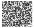
- FIG. 4 is an optical microscope image taken by optically polishing a cut surface of the silica glass member according to Example 1.
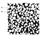
- FIG. FIG. 5 is an optical microscope image taken by optically polishing a cut surface of the silica glass member according to Example 3.
- FIG. 6A is a diagram for explaining a method for calculating the average bubble diameter, and is an X-ray CT image from which noise has been removed for a sample obtained by optically polishing the surface of the evaluation object.
- FIG. 6B is a diagram for explaining a method of calculating the average bubble diameter, and is an image after binarization processing of FIG. 6A.
- FIG. 6C is a diagram for explaining a method of calculating the average bubble diameter, and is an image after the watershed division processing of FIG. 6B.
- FIG. 1(A) is a perspective view of the silica glass member 1
- FIG. 1(B) is a cross-sectional view taken along line XX' of (A).
- the silica glass member 1 shown in FIG. 1A is a rectangular parallelepiped, its shape is not particularly limited. When used as a dummy wafer, it preferably has substantially the same shape as the product wafer.
- the silica glass member 1 has a silica glass portion 10 and a plurality of bubbles 12 .
- the air bubbles 12 include non-communication air bubbles 14 and communication air bubbles 16 .
- the silica glass portion 10 is mainly composed of amorphous silicon oxide (SiO 2 ) and is transparent. Also, its density is about 2.2 g/cm 3 . In addition to SiO 2 , the silica glass portion 10 may contain different elements for the purpose of controlling the properties of the silica glass portion 10 .
- SiO 2 amorphous silicon oxide
- the silica glass portion 10 may contain different elements for the purpose of controlling the properties of the silica glass portion 10 .
- the non-communication bubbles 14 are distributed substantially uniformly in the silica glass member 1 and contain gas inside.
- the shape of the non-communication cell 14 is not particularly limited, it is substantially spherical or substantially flat spherical.
- the communicating air bubbles 16 are formed by connecting adjacent non-communicating air bubbles 14 to each other.
- FIG. 1B two-dimensional communication is depicted, but there are also cases where three-dimensional communication is possible.
- Some or all of the cells 12 contained in the silica glass member 1 form communicating cells 16 .
- a plurality of pits 18 are present on the surface of the silica glass member 1 .
- the pits 18 are formed by the non-communicating cells 14 or communicating cells 16 exposed on the surface.
- the pits 18 have a substantially circular shape, a substantially elliptical shape, or a shape in which these are connected. Since the silica glass member 1 having the pits 18 has an increased surface area, it is suitable as a dummy wafer.
- the value obtained by dividing the surface area S of the silica glass member 1 by the geometric surface area S0 calculated based on the outer dimensions of the silica glass member 1 is 1.5 or more, preferably 3 or more, and more It is preferably 4 or more, more preferably 5 or more, even more preferably 6 or more, and most preferably 8 or more. If S/S0 is 1.5 or more, it can be said that the surface area of the silica glass member 1 is sufficiently large, so that the uniformity of film formation on product wafers is improved.
- the geometric surface area S0 is an imaginary surface area obtained by assuming that the surface of the silica glass member 1 is flat without the pits 18 present.
- the lower limit of the average bubble diameter of the bubbles 12 is preferably 30 ⁇ m, more preferably 40 ⁇ m, still more preferably 50 ⁇ m, and the upper limit is preferably 150 ⁇ m, more preferably 120 ⁇ m. If the average cell diameter is within this range, the effect of increasing the surface area can be sufficiently obtained.
- the average bubble diameter is the average value of the bubble diameters calculated on the assumption that the shape of the bubbles is a perfect circle.
- the communication bubble 16 is divided into a plurality of regions by a method described later, and the diameter of the bubble is obtained by regarding the divided regions as one bubble.
- the lower limit of the bulk density of the silica glass member 1 is preferably 0.3 g/cm 3 , more preferably 0.5 g/cm 3
- the upper limit is preferably 2 g/cm 3 , more preferably 1.6 g/cm 3 . 3 . If the bulk density is 0.3 g/cm 3 or more, sufficient strength of the silica glass member 1 can be obtained. Also, if the bulk density is 2 g/cm 3 or less, the silica glass member 1 will contain a sufficient number of bubbles 12 and the surface area will increase, so that it can be suitably used as a dummy wafer.
- the ratio of the number of communicating cells 16 to the number of multiple cells 12 (the sum of the number of non-communicating cells 14 and the number of communicating cells 16) (hereinafter referred to as the communicating cell rate) is preferably 30% or more, more preferably. is 50% or more, more preferably 70% or more. If the communicating bubble ratio is 30% or more, the probability that the bubbles forming the pits 18 are the communicating bubbles 16 increases, and as a result the surface area of the dummy wafer is sufficiently increased.
- the silica glass portion 10 contains lithium (Li), sodium (Na), magnesium (Mg), aluminum (Al), potassium (K), calcium (Ca), chromium (Cr), manganese (Mn), and iron (Fe). , nickel (Ni), copper (Cu), titanium (Ti), cobalt (Co), zinc (Zn), silver (Ag), cadmium (Cd) and lead (Pb), respectively. It is preferably 0.5 mass ppm or less, more preferably 0.1 mass ppm or less. If the content of each metal impurity is 0.5 ppm by mass or less, it can be suitably used as a member used in a semiconductor manufacturing apparatus. In the specification, ppm means parts per million, and ppb means parts per billion.
- the silica glass member 1 having the structure as described above has fewer places where chipping can occur, compared to a dummy wafer on which an uneven pattern is formed, so that particles are less likely to occur.
- the silica glass member 1 is also advantageous from the viewpoint of washing resistance.
- the dummy wafer is usually cleaned by dry etching using a fluorine-based gas or the like or wet etching using hydrofluoric acid or the like.
- the dummy wafer on which the unevenness pattern is formed may be likely to become substantially flat due to the corners of the unevenness being scraped off, resulting in a reduction in the surface area.
- the silica glass member 1 is suppressed from decreasing in surface area due to cleaning.
- a change in the surface area of the silica glass member 1 during cleaning will be described with reference to FIG. In FIG. 2, it is assumed that only the upper surface of the silica glass member 1 having three pits (18a, 18b, 18c) is cleaned. At this time, the upper surface of the silica glass member 1 and the inner wall surfaces of the pits are etched by washing, and as a result, the pits 18b and 18c disappear. 18e and 18f are formed. In this way, the silica glass member 1 has the air bubbles 12 therein, thereby suppressing the reduction of the surface area due to washing.
- a method for manufacturing the silica glass member 1 according to this embodiment will be described with reference to FIG.
- a VAD (Vapor-phase Axial Deposition) method is used as a method for synthesizing silica glass.
- the method for manufacturing the silica glass member 1 has steps S21 to S25.
- synthetic raw materials for silica glass are selected.
- Synthetic raw materials for silica glass are not particularly limited as long as they are gasifiable silicon-containing raw materials, but typically silicon chlorides (eg, SiCl 4 , SiHCl 3 , SiH 2 Cl 2 , SiCH 3 Cl 3 ) and silicon fluorides are used.
- halogen-containing silicon compounds such as SiF 4 , SiHF 3 , SiH 2 F 2 , or RnSi(OR) 4-n (R: alkyl group having 1 to 4 carbon atoms, n: an integer of 0 to 3)
- alkoxysilanes represented by and halogen-free silicon compounds such as (CH 3 ) 3 Si—O—Si(CH 3 ) 3 .
- step S22 the synthetic raw material is flame hydrolyzed at a temperature of 1000°C to 1500°C to generate silica particles, which are deposited on a rotating substrate by spraying to obtain a soot body.
- silica particles are partly sintered together.
- the soot body may be heat-treated in a vacuum atmosphere to dehydrate and reduce the OH group concentration.
- the temperature during the heat treatment is preferably 1000° C. to 1300° C., and the treatment time is preferably 1 hour to 240 hours.
- step S23 the soot body is subjected to high-temperature and high-pressure treatment in an inert gas atmosphere, so that the silica particles in the soot body are sintered together and densified to obtain a silica glass dense body.
- the silica glass dense body is transparent silica glass containing almost no bubbles or opaque silica glass containing minute bubbles.
- the temperature during the high temperature and high pressure treatment is 1200° C. to 1700° C.
- the pressure is 0.01 MPa to 200 MPa
- the treatment time is 10 hours to 100 hours.
- the inert gas is dissolved in silica glass.
- Inert gases typically include helium (He), neon (Ne), argon (Ar), krypton (Kr), xenon (Xe), nitrogen ( N2 ), or at least two or more of these. It is a mixed gas, and although details will be described later, it is preferably Ar. It is generally known that the solubility of an inert gas in silica glass tends to decrease as the partial pressure of the inert gas in the atmosphere decreases or as the temperature of the silica glass increases.
- step S24 the silica glass dense body is subjected to a high temperature and low pressure treatment, whereby the inert gas dissolved in the silica glass is foamed and the bubbles contained in the silica glass dense body are thermally expanded.
- a silica glass porous body made porous and having air bubbles 12 is obtained.
- the temperature during the high temperature and low pressure treatment is 1300° C. to 1800° C.
- the pressure is 0 Pa to 0.1 MPa
- the treatment time is 1 minute to 20 hours. Note that if the treatment time is within 20 hours, there is no fear that the bubbles 12 will be closed due to excessive heating.
- step S24 if the treatment is performed at a lower pressure or a higher temperature than in step S23, the dissolved amount of the inert gas may become supersaturated, and at this time bubbles will occur in the silica glass. .
- foaming can occur even if the temperature during the high-temperature, low-pressure treatment in step S24 is lower than the temperature during the high-temperature, high-pressure treatment in step S23. is promoted, and porosity tends to progress.
- Ar is preferable from the viewpoint that while it is relatively inexpensive, the temperature dependence of the solubility in silica glass is large, and it is easy to control the porosity.
- the number of bubbles 12 contained in the silica glass member 1 is increased.
- the number, bubble diameter, bulk density, etc. can be controlled.
- the silica glass member 1 is obtained by processing the silica glass porous body into an arbitrary shape using methods such as cutting, slicing, grinding, and polishing.
- the silica glass member 1 is used as a dummy wafer, it preferably has substantially the same shape as the product wafer.
- the silica glass member 1 suitable as a dummy wafer can be obtained without performing complicated and expensive machining for forming an uneven pattern.
- silica glass member 1 is not limited to dummy wafers, and can be applied to various uses within the range in which the properties of the silica glass member 1 described in this specification work advantageously.
- Silicon tetrachloride (SiCl 4 ) was selected as a synthetic raw material for silica glass, flame hydrolyzed to generate silica particles, and deposited on a rotating substrate by spraying to obtain a soot body.
- the soot body is placed in a heating furnace, filled with Ar gas, subjected to high temperature and high pressure treatment at a predetermined temperature, pressure and treatment time to densify the soot body, and then returned to the atmospheric pressure and left to cool. did.
- the silica glass dense body obtained at this time was an opaque silica glass containing minute air bubbles.
- Silica glass members 1 having the parameters shown in Examples 1 to 5 in Table 1 were obtained by arbitrarily combining the temperature, pressure, and treatment time in the high-temperature, high-pressure treatment and the high-temperature, low-pressure treatment. Examples 1-5 are examples.
- FIG. 4 shows an optical microscope image of the surface of the silica glass member 1 of Example 1 taken after optical polishing.
- the silica glass member 1 of Example 1 there are bubbles 12 dispersed substantially uniformly, some of which exist as communicating bubbles 16, and S/S0 is 1.9. Met.
- the silica glass member 1 of Example 1 Li, Mg, K, Cr, Mn, Fe, Ni, Cu, Ti, Co, Zn, Ag, Cd, Ce and Pb Less than 3 ppb, Na 80 ppb, Al 30 ppb, Ca 10 ppb.
- the content of metal impurities was determined by an ICP-MS (Inductively Coupled Plasma-Mass Spectrometer) method after cutting the silica gas member 1 obtained above into an appropriate size.
- FIG. 5 shows an optical microscope image of the surface of the silica glass member 1 of Example 4 taken after optical polishing.
- substantially uniformly dispersed cells 12 exist, some of which exist as communicating cells 16.
- the S/S0 was a high value of 6.9 due to the large average cell diameter and the high open cell ratio.
- the silica glass member 1 of Examples 1 to 5 has a large surface area due to the inclusion of the air bubbles 12 without machining, and the structure suppresses the generation of particles. It can be suitably used as a dummy wafer.
- the surface area S was determined by the BET method according to JIS-Z8830:2013. Specifically, five 40 mm ⁇ 8 mm ⁇ 0.5 mm plate-shaped samples were prepared from the object to be evaluated. After that, adsorption measurement of krypton (Kr) gas was performed using a specific surface area measuring device (BELSORP-max manufactured by Nippon Bell Co., Ltd.), and the surface area S was obtained by dividing the obtained value by 5 (the number of samples). S/S0 was obtained by dividing this by the geometric surface area S0 based on the external dimensions of the sample.
- Kr krypton
- the average bubble diameter was obtained by the following procedures (I) to (IV).
- Denoising using eg, ImageJ
- FIG. 6B the threshold value of the brightness value of the binarization process was determined so that the ratio of the area of the white region (corresponding to the bubble 12) to the area of the entire image in FIG.
- FIG. 6C An image such as that shown in FIG. 6C was obtained by performing a process of dividing the communicating bubbles by the watershed division process.
- the watershed partitioning process is performed by the following procedure: Create a Euclidean Distance Map (EDM) for the image of FIG. 6B and find the Ultimate Erosion Point (UEP), which is the maximum or vertex of the EDM; Expand each UEP until it reaches the edge of each bubble, or until it reaches the edge of the UEP region expanding with communicating bubbles; Divide the communicating cells based on their respective expanded UEP regions.
- EDM Euclidean Distance Map
- UEP Ultimate Erosion Point
- silica glass member 10 silica glass part 12 bubble 14 non-communication bubble 16 open air bubble 18 pit
Abstract
Description
凹凸パターンが形成されたダミーウエハにおいて、表面積を更に向上させるには、通常、凹凸のピッチを狭くする必要がある。ところが、ピッチが狭い凹凸を形成すると、凸部が細長い形状となるので、欠けが生じやすくなる場合がある。欠けは、パーティクルとなり、歩留り低下の原因となり得る。 By the way, the concave and convex patterns of product wafers are becoming finer year by year, and along with this, there is a need to further increase the surface area of dummy wafers.
In order to further improve the surface area of a dummy wafer on which an uneven pattern is formed, it is usually necessary to narrow the pitch of the unevenness. However, when the unevenness is formed with a narrow pitch, the protrusions have a long and narrow shape, which may easily cause chipping. Chipping becomes particles and can cause a decrease in yield.
[1] 複数の気泡を有し、
前記複数の気泡の一部または全部は連通気泡であり、
S/S0が1.5以上である、シリカガラス部材。
S:前記シリカガラス部材から切り出した40mm×8mm×0.5mmのサンプルについてBET法により求めた表面積
S0:前記サンプルの外形寸法に基づいて求めた幾何表面積
[2] 前記S/S0は4以上である、[1]に記載のシリカガラス部材。
[3] 前記S/S0は5以上である、[1]に記載のシリカガラス部材。
[4] X線CT像の画像解析により求められる前記気泡の平均気泡径が30μm~150μmである、[1]~[3]のいずれかに記載のシリカガラス部材。
[5] かさ密度が0.3g/cm3~2g/cm3である、[1]~[4]のいずれかに記載のシリカガラス部材。
[6] 前記複数の気泡の個数に対する前記連通気泡の個数の比率が30%~100%である、[1]~[5]のいずれかに記載のシリカガラス部材。
[7] 前記複数の気泡の個数に対する前記連通気泡の個数の比率が70%~100%である、[1]~[5]のいずれかに記載のシリカガラス部材。
[8] リチウム(Li)、アルミニウム(Al)、クロム(Cr)、マンガン(Mn)、ニッケル(Ni)、銅(Cu)、チタン(Ti)、コバルト(Co)、亜鉛(Zn)、銀(Ag)、カドミウム(Cd)、鉛(Pb)、ナトリウム(Na)、マグネシウム(Mg)、カリウム(K)、カルシウム(Ca)、セリウム(Ce)および鉄(Fe)の各金属不純物の含有量がそれぞれ0.5質量ppm以下である、[1]~[7]のいずれかに記載のシリカガラス部材。
[9] 半導体製造における縦型熱処理装置用のダミーウエハとして用いられる、[1]~[8]のいずれかに記載のシリカガラス部材。
[10] 複数の気泡を有し、前記複数の気泡の一部または全部は連通気泡であり、前記シリカガラス部材から切り出した40mm×8mm×0.5mmのサンプルについてBET法により求めた表面積をSとし、前記サンプルの外形寸法に基づいて求めた幾何表面積をSOとしたとき、S/S0が1.5以上である、シリカガラス部材を製造する方法であって、
ケイ素化合物を火炎加水分解して生成したシリカ粒子を堆積させてスート体を得ることと、
前記スート体を不活性ガス雰囲気下にて緻密化しシリカガラス緻密体を得ることと、
前記シリカガラス緻密体を得たときより少なくとも低圧または高温の条件下にて前記シリカガラス緻密体を多孔質化することによりシリカガラス多孔質体を得ることと、
前記シリカガラス多孔質体を加工して任意の形状のシリカガラス部材を得ることと、
を含む、シリカガラス部材の製造方法。 The present invention relates to the following [1] to [10].
[1] having a plurality of bubbles,
Some or all of the plurality of bubbles are communicating bubbles,
A silica glass member having an S/S0 of 1.5 or more.
S: surface area obtained by the BET method for a 40 mm × 8 mm × 0.5 mm sample cut from the silica glass member S0: geometric surface area obtained based on the external dimensions of the sample [2] The S/S0 is 4 or more. The silica glass member according to [1].
[3] The silica glass member according to [1], wherein S/S0 is 5 or more.
[4] The silica glass member according to any one of [1] to [3], wherein the average bubble diameter of the bubbles determined by image analysis of X-ray CT images is 30 μm to 150 μm.
[5] The silica glass member according to any one of [1] to [4], which has a bulk density of 0.3 g/cm 3 to 2 g/cm 3 .
[6] The silica glass member according to any one of [1] to [5], wherein the ratio of the number of the communicating cells to the number of the plurality of cells is 30% to 100%.
[7] The silica glass member according to any one of [1] to [5], wherein the ratio of the number of the communicating cells to the number of the plurality of cells is 70% to 100%.
[8] Lithium (Li), aluminum (Al), chromium (Cr), manganese (Mn), nickel (Ni), copper (Cu), titanium (Ti), cobalt (Co), zinc (Zn), silver ( Ag), cadmium (Cd), lead (Pb), sodium (Na), magnesium (Mg), potassium (K), calcium (Ca), cerium (Ce) and iron (Fe). The silica glass member according to any one of [1] to [7], each of which is 0.5 mass ppm or less.
[9] The silica glass member according to any one of [1] to [8], which is used as a dummy wafer for vertical heat treatment equipment in semiconductor manufacturing.
[10] A sample having a plurality of bubbles, some or all of which are interconnected bubbles, and a sample of 40 mm × 8 mm × 0.5 mm cut out from the silica glass member, the surface area obtained by the BET method is S A method for producing a silica glass member, wherein S/S0 is 1.5 or more, where SO is the geometric surface area obtained based on the external dimensions of the sample,
obtaining a soot body by accumulating silica particles produced by flame hydrolysis of a silicon compound;
densifying the soot body in an inert gas atmosphere to obtain a silica glass dense body;
obtaining a silica glass porous body by making the silica glass dense body porous under conditions at least at a lower pressure or a higher temperature than when the silica glass dense body was obtained;
obtaining a silica glass member having an arbitrary shape by processing the silica glass porous body;
A method for producing a silica glass member, comprising:
図1の(A)は、シリカガラス部材1の斜視図であり、図1の(B)は、(A)のX-X’矢視断面図である。
図1の(A)に示すシリカガラス部材1は直方体であるが、形状は特に限定されない。ダミーウエハとして用いる場合は、製品ウエハと略同一の形状であることが好ましい。
図1の(B)にて示すように、シリカガラス部材1は、シリカガラス部10と、複数の気泡12を有する。気泡12は、非連通気泡14と、連通気泡16とを含む。 First, the structure of a
FIG. 1(A) is a perspective view of the
Although the
As shown in FIG. 1B, the
シリカガラス部材1の表面積Sを、シリカガラス部材1の外形寸法に基づいて計算される幾何表面積S0で除した値(S/S0)は1.5以上であり、好ましくは3以上であり、より好ましくは4以上であり、さらに好ましくは5以上であり、よりさらに好ましくは6以上であり、最も好ましくは8以上である。S/S0が1.5以上であれば、シリカガラス部材1の表面積が十分に大きいと言えるので、製品ウエハに対する成膜の均一性が向上する。また、S/S0が大きければ大きいほど、近年の微細化が進んだ製品ウエハとともに用いるダミーウエハとしては好適となる場合がある。なお、幾何表面積S0とは、シリカガラス部材1の表面が、ピット18の存在しない平坦面であると仮定して求められる仮想の表面積である。 Next, the characteristics of the
The value obtained by dividing the surface area S of the
通常、使用後のダミーウエハは、フッ素系ガス等によるドライエッチングや、フッ酸等によるウェットエッチングにより洗浄される。このとき、凹凸パターンが形成されたダミーウエハは、その凹凸形状によっては、凹凸の角部が削られて略平坦となりやすい場合があり、表面積が減少してしまう。 The
After use, the dummy wafer is usually cleaned by dry etching using a fluorine-based gas or the like or wet etching using hydrofluoric acid or the like. At this time, depending on the shape of the unevenness, the dummy wafer on which the unevenness pattern is formed may be likely to become substantially flat due to the corners of the unevenness being scraped off, resulting in a reduction in the surface area.
本実施形態においては、シリカガラスの合成方法としてVAD(Vapor-phase Axial Deposition)法を用いているが、本発明の効果を奏する限りにおいて、製造方法は適宜変更しても構わない。 Next, a method for manufacturing the
In this embodiment, a VAD (Vapor-phase Axial Deposition) method is used as a method for synthesizing silica glass.
ステップS21では、シリカガラスの合成原料を選定する。シリカガラスの合成原料は、ガス化可能なケイ素含有原料であれば特に制限されないが、代表的にはケイ素塩化物(例えばSiCl4,SiHCl3,SiH2Cl2,SiCH3Cl3)やケイ素フッ化物(例えばSiF4,SiHF3,SiH2F2)といったハロゲンを含むケイ素化合物、または、RnSi(OR)4-n(R:炭素数1~4のアルキル基、n:0~3の整数)で示されるアルコキシシランや(CH3)3Si-O-Si(CH3)3といったハロゲンを含まないケイ素化合物が挙げられる。 As shown in FIG. 3, the method for manufacturing the
In step S21, synthetic raw materials for silica glass are selected. Synthetic raw materials for silica glass are not particularly limited as long as they are gasifiable silicon-containing raw materials, but typically silicon chlorides (eg, SiCl 4 , SiHCl 3 , SiH 2 Cl 2 , SiCH 3 Cl 3 ) and silicon fluorides are used. halogen-containing silicon compounds such as SiF 4 , SiHF 3 , SiH 2 F 2 , or RnSi(OR) 4-n (R: alkyl group having 1 to 4 carbon atoms, n: an integer of 0 to 3) Examples thereof include alkoxysilanes represented by and halogen-free silicon compounds such as (CH 3 ) 3 Si—O—Si(CH 3 ) 3 .
シリカガラスの合成原料として、四塩化ケイ素(SiCl4)を選定し、これを火炎加水分解してシリカ粒子を生成し、回転する基材上に吹き付けて堆積させることにより、スート体を得た。次に、このスート体を加熱炉内に配し、Arガスを充填し、所定の温度、圧力および処理時間にて高温高圧処理を行い、スート体を緻密化した後、大気圧に戻し放冷した。このとき得られたシリカガラス緻密体は、微小な気泡を含む不透明シリカガラスであった。次に、所定の温度および処理時間にて高温低圧処理を行い、シリカガラス緻密体を多孔質化した後、大気圧に戻して放冷し、シリカガラス多孔質体を得た。最後に、シリカガラス多孔質体を炉から取り出し、切断加工、スライス加工、研削加工、研磨加工によって所望の形状とした。上記高温高圧処理および上記高温低圧処理における温度、圧力および処理時間を任意に組み合わせることで、表1の例1~5に示すパラメータを有するシリカガラス部材1がそれぞれ得られた。
例1~5は実施例である。 (Examples 1-5)
Silicon tetrachloride (SiCl 4 ) was selected as a synthetic raw material for silica glass, flame hydrolyzed to generate silica particles, and deposited on a rotating substrate by spraying to obtain a soot body. Next, the soot body is placed in a heating furnace, filled with Ar gas, subjected to high temperature and high pressure treatment at a predetermined temperature, pressure and treatment time to densify the soot body, and then returned to the atmospheric pressure and left to cool. did. The silica glass dense body obtained at this time was an opaque silica glass containing minute air bubbles. Next, a high-temperature and low-pressure treatment was performed at a predetermined temperature and treatment time to make the silica glass dense body porous. Finally, the silica glass porous body was taken out of the furnace and cut, sliced, ground, and polished into a desired shape.
Examples 1-5 are examples.
(S/S0)
表面積Sは、JIS―Z8830:2013によるBET法により求めた。具体的には、評価対象物を40mm×8mm×0.5mmの板状に切り出したサンプルを5枚作製し、これらをガラスセルに入れて、前処理として200℃で約5時間減圧脱気した後、比表面積測定装置(日本ベル社製:BELSORP-max)によりクリプトン(Kr)ガスの吸着測定を行い、得られた値を5(サンプルの枚数)で除することで表面積Sを求めた。これを、サンプルの外形寸法に基づく幾何表面積S0で除することにより、S/S0を求めた。 Each parameter shown in Table 1 was determined by the method shown below.
(S/S0)
The surface area S was determined by the BET method according to JIS-Z8830:2013. Specifically, five 40 mm × 8 mm × 0.5 mm plate-shaped samples were prepared from the object to be evaluated. After that, adsorption measurement of krypton (Kr) gas was performed using a specific surface area measuring device (BELSORP-max manufactured by Nippon Bell Co., Ltd.), and the surface area S was obtained by dividing the obtained value by 5 (the number of samples). S/S0 was obtained by dividing this by the geometric surface area S0 based on the external dimensions of the sample.
平均気泡径は、以下の(I)~(IV)の手順により求めた。
(I)まず、評価対象物の表面を光学研磨して得られたサンプルについて、X線CT装置(テスコ社製:TXS-CT300)を用いてX線CT像を取得し、これ対し画像処理ソフト(例えば、ImageJ)を用いてノイズ除去することで、図6Aのような画像を得た。
(II)次に、画像処理ソフト(例えば、ImageJ)を用いて二値化処理を行い、図6Bのような画像を得た。このとき、二値化処理の輝度値の閾値は、図6Bの画像全体の面積に対する白色領域(気泡12に相当)の面積の比率が、評価対象物の気泡率と最も近くなるように決定した。ここで、気泡率は、気泡を略含まないシリカガラスの密度が2.2g/cm3であることから、後述するかさ密度ρを用いて、下記式(1)より求められる。なお、図6Bにおいて、画像端部で切れている白色領域については、平均気泡径の算出においては無視した。 (Average bubble diameter)
The average bubble diameter was obtained by the following procedures (I) to (IV).
(I) First, for a sample obtained by optically polishing the surface of the object to be evaluated, an X-ray CT image is obtained using an X-ray CT device (manufactured by Tesco: TXS-CT300). Denoising using (eg, ImageJ) yielded an image as shown in FIG. 6A.
(II) Next, binarization processing was performed using image processing software (for example, ImageJ) to obtain an image as shown in FIG. 6B. At this time, the threshold value of the brightness value of the binarization process was determined so that the ratio of the area of the white region (corresponding to the bubble 12) to the area of the entire image in FIG. 6B was closest to the bubble ratio of the evaluation object. . Here, since the density of silica glass substantially free of bubbles is 2.2 g/cm 3 , the bubble ratio is obtained from the following formula (1) using the bulk density ρ, which will be described later. In addition, in FIG. 6B, the white region cut off at the edge of the image was ignored in the calculation of the average bubble diameter.

図6Bの画像に対しユークリッド距離マップ(EDM)を作成し、EDMの極大または頂点である極限浸食点(UEP)を検出する;
各UEPを各気泡の端に到達するまで、または、連通気泡にて拡張しているUEP領域の縁に到達するまで拡張させる;
それぞれの拡張したUEP領域に基づいて連通気泡を分割する。 (III) Next, an image such as that shown in FIG. 6C was obtained by performing a process of dividing the communicating bubbles by the watershed division process. Here, the watershed partitioning process is performed by the following procedure:
Create a Euclidean Distance Map (EDM) for the image of FIG. 6B and find the Ultimate Erosion Point (UEP), which is the maximum or vertex of the EDM;
Expand each UEP until it reaches the edge of each bubble, or until it reaches the edge of the UEP region expanding with communicating bubbles;
Divide the communicating cells based on their respective expanded UEP regions.

評価対象物を40mm×8mm×0.5mmの直方体状に切り出し、電子天秤により質量を測定した。これを、サンプルの見掛け体積で除することによって、かさ密度を求めた。 (bulk density)
An object to be evaluated was cut into a rectangular parallelepiped of 40 mm×8 mm×0.5 mm, and the mass was measured with an electronic balance. The bulk density was obtained by dividing this by the apparent volume of the sample.
上述した図6Cにおいて分割がなされなかった白色領域を非連通気泡、分割がなされた白色領域を連通気泡とみなし、連通気泡の個数を気泡の総数(非連通気泡の個数と連通気泡の個数との和)で除することで、連通気泡率を求めた。なお、図6Cにおいて、画像端部で切れている白色領域については、連通気泡率の算出においては無視した。 (Communication bubble rate)
In FIG. 6C described above, the undivided white regions are regarded as non-communicating bubbles, and the divided white regions are regarded as communicating bubbles, and the number of communicating bubbles is the total number of bubbles (the number of non-communicating bubbles and the number of communicating bubbles). sum) to determine the open cell ratio. In addition, in FIG. 6C, the white region cut off at the edge of the image was ignored in the calculation of the interconnected cell ratio.

10 シリカガラス部
12 気泡
14 非連通気泡
16 連通気泡
18 ピット 1
16
Claims (10)
- 複数の気泡を有し、
前記複数の気泡の一部または全部は連通気泡であり、
S/S0が1.5以上である、シリカガラス部材。
S:前記シリカガラス部材から切り出した40mm×8mm×0.5mmのサンプルについてBET法により求めた表面積
S0:前記サンプルの外形寸法に基づいて求めた幾何表面積 having multiple bubbles,
Some or all of the plurality of bubbles are communicating bubbles,
A silica glass member having an S/S0 of 1.5 or more.
S: Surface area determined by BET method for a 40 mm × 8 mm × 0.5 mm sample cut from the silica glass member S0: Geometric surface area determined based on the external dimensions of the sample - 前記S/S0は4以上である、請求項1に記載のシリカガラス部材。 The silica glass member according to claim 1, wherein said S/S0 is 4 or more.
- 前記S/S0は5以上である、請求項1に記載のシリカガラス部材。 The silica glass member according to claim 1, wherein said S/S0 is 5 or more.
- X線CT像の画像解析により求められる前記気泡の平均気泡径が30μm~150μmである、請求項1~3のいずれか1項に記載のシリカガラス部材。 The silica glass member according to any one of claims 1 to 3, wherein the average bubble diameter of the bubbles obtained by image analysis of X-ray CT images is 30 µm to 150 µm.
- かさ密度が0.3g/cm3~2g/cm3である、請求項1~4のいずれか1項に記載のシリカガラス部材。 The silica glass member according to any one of claims 1 to 4, which has a bulk density of 0.3 g/cm 3 to 2 g/cm 3 .
- 前記複数の気泡の個数に対する前記連通気泡の個数の比率が30%~100%である、請求項1~5のいずれか1項に記載のシリカガラス部材。 The silica glass member according to any one of claims 1 to 5, wherein the ratio of the number of said communicating cells to the number of said plurality of cells is 30% to 100%.
- 前記複数の気泡の個数に対する前記連通気泡の個数の比率が70%~100%である、請求項1~5のいずれか1項に記載のシリカガラス部材。 The silica glass member according to any one of claims 1 to 5, wherein the ratio of the number of said communicating cells to the number of said plurality of cells is 70% to 100%.
- リチウム(Li)、アルミニウム(Al)、クロム(Cr)、マンガン(Mn)、ニッケル(Ni)、銅(Cu)、チタン(Ti)、コバルト(Co)、亜鉛(Zn)、銀(Ag)、カドミウム(Cd)、鉛(Pb)、ナトリウム(Na)、マグネシウム(Mg)、カリウム(K)、カルシウム(Ca)、セリウム(Ce)および鉄(Fe)の各金属不純物の含有量がそれぞれ0.5質量ppm以下である、請求項1~7のいずれか1項に記載のシリカガラス部材。 Lithium (Li), aluminum (Al), chromium (Cr), manganese (Mn), nickel (Ni), copper (Cu), titanium (Ti), cobalt (Co), zinc (Zn), silver (Ag), Contents of metal impurities of cadmium (Cd), lead (Pb), sodium (Na), magnesium (Mg), potassium (K), calcium (Ca), cerium (Ce) and iron (Fe) are respectively 0.00. The silica glass member according to any one of claims 1 to 7, which is 5 mass ppm or less.
- 半導体製造における縦型熱処理装置用のダミーウエハとして用いられる、請求項1~8のいずれか1項に記載のシリカガラス部材。 The silica glass member according to any one of claims 1 to 8, which is used as a dummy wafer for a vertical heat treatment apparatus in semiconductor manufacturing.
- 複数の気泡を有し、前記複数の気泡の一部または全部は連通気泡であり、前記シリカガラス部材から切り出した40mm×8mm×0.5mmのサンプルについてBET法により求めた表面積をSとし、前記サンプルの外形寸法に基づいて求めた幾何表面積をSOとしたとき、S/S0が1.5以上である、シリカガラス部材を製造する方法であって、
ケイ素化合物を火炎加水分解して生成したシリカ粒子を堆積させてスート体を得ることと、
前記スート体を不活性ガス雰囲気下にて緻密化しシリカガラス緻密体を得ることと、
前記シリカガラス緻密体を得たときより少なくとも低圧または高温の条件下にて前記シリカガラス緻密体を多孔質化することによりシリカガラス多孔質体を得ることと、
前記シリカガラス多孔質体を加工して任意の形状のシリカガラス部材を得ることと、
を含む、シリカガラス部材の製造方法。 S is the surface area of a sample of 40 mm × 8 mm × 0.5 mm cut out from the silica glass member, which has a plurality of bubbles, some or all of which are communicating bubbles, obtained by the BET method, A method for producing a silica glass member, wherein S/S0 is 1.5 or more, where SO is the geometric surface area determined based on the external dimensions of the sample,
obtaining a soot body by accumulating silica particles produced by flame hydrolysis of a silicon compound;
densifying the soot body in an inert gas atmosphere to obtain a silica glass dense body;
obtaining a silica glass porous body by making the silica glass dense body porous under conditions at least at a lower pressure or a higher temperature than when the silica glass dense body was obtained;
obtaining a silica glass member having an arbitrary shape by processing the silica glass porous body;
A method for producing a silica glass member, comprising:
Priority Applications (5)
| Application Number | Priority Date | Filing Date | Title |
|---|---|---|---|
| JP2023513005A JPWO2022215663A1 (en) | 2021-04-07 | 2022-03-31 | |
| DE112022002001.6T DE112022002001T5 (en) | 2021-04-07 | 2022-03-31 | QUARTZ GLASS ELEMENT AND METHOD FOR THE PRODUCTION THEREOF |
| KR1020237033332A KR20230167358A (en) | 2021-04-07 | 2022-03-31 | Silica glass member and method of manufacturing the same |
| CN202280025606.3A CN117083252A (en) | 2021-04-07 | 2022-03-31 | Silica glass member and method for producing same |
| US18/479,852 US20240025795A1 (en) | 2021-04-07 | 2023-10-03 | Silica glass member and method for producing same |
Applications Claiming Priority (4)
| Application Number | Priority Date | Filing Date | Title |
|---|---|---|---|
| JP2021065433 | 2021-04-07 | ||
| JP2021-065433 | 2021-04-07 | ||
| JP2021135895 | 2021-08-23 | ||
| JP2021-135895 | 2021-08-23 |
Related Child Applications (1)
| Application Number | Title | Priority Date | Filing Date |
|---|---|---|---|
| US18/479,852 Continuation US20240025795A1 (en) | 2021-04-07 | 2023-10-03 | Silica glass member and method for producing same |
Publications (1)
| Publication Number | Publication Date |
|---|---|
| WO2022215663A1 true WO2022215663A1 (en) | 2022-10-13 |
Family
ID=83546077
Family Applications (1)
| Application Number | Title | Priority Date | Filing Date |
|---|---|---|---|
| PCT/JP2022/016901 WO2022215663A1 (en) | 2021-04-07 | 2022-03-31 | Silica glass member and method for producing same |
Country Status (6)
| Country | Link |
|---|---|
| US (1) | US20240025795A1 (en) |
| JP (1) | JPWO2022215663A1 (en) |
| KR (1) | KR20230167358A (en) |
| DE (1) | DE112022002001T5 (en) |
| TW (1) | TW202306917A (en) |
| WO (1) | WO2022215663A1 (en) |
Citations (5)
| Publication number | Priority date | Publication date | Assignee | Title |
|---|---|---|---|---|
| JPH1029836A (en) * | 1996-07-15 | 1998-02-03 | Shinetsu Quartz Prod Co Ltd | Production of quartz glass expanded body |
| JPH1192167A (en) * | 1997-09-22 | 1999-04-06 | Toshiba Ceramics Co Ltd | Porous quartz glass and its production |
| JP2002362967A (en) * | 2001-06-06 | 2002-12-18 | Koransha Co Ltd | Member for semiconductor wafer etching consisting of silica glass sintered compact and production method therefor |
| JP2007238419A (en) * | 2006-03-13 | 2007-09-20 | Tosoh Quartz Corp | Opaque sintered compact |
| JP2015173154A (en) * | 2014-03-11 | 2015-10-01 | 東京エレクトロン株式会社 | Vertical heat treatment apparatus, operation method of vertical heat treatment apparatus and storage medium |
Family Cites Families (2)
| Publication number | Priority date | Publication date | Assignee | Title |
|---|---|---|---|---|
| JP2021065433A (en) | 2019-10-23 | 2021-04-30 | 日本製紙クレシア株式会社 | Absorbent article |
| JP2021135895A (en) | 2020-02-28 | 2021-09-13 | 三菱重工業株式会社 | Detection device, detection method, robot, and program |
-
2022
- 2022-03-31 KR KR1020237033332A patent/KR20230167358A/en unknown
- 2022-03-31 JP JP2023513005A patent/JPWO2022215663A1/ja active Pending
- 2022-03-31 WO PCT/JP2022/016901 patent/WO2022215663A1/en active Application Filing
- 2022-03-31 DE DE112022002001.6T patent/DE112022002001T5/en active Pending
- 2022-04-01 TW TW111112902A patent/TW202306917A/en unknown
-
2023
- 2023-10-03 US US18/479,852 patent/US20240025795A1/en active Pending
Patent Citations (5)
| Publication number | Priority date | Publication date | Assignee | Title |
|---|---|---|---|---|
| JPH1029836A (en) * | 1996-07-15 | 1998-02-03 | Shinetsu Quartz Prod Co Ltd | Production of quartz glass expanded body |
| JPH1192167A (en) * | 1997-09-22 | 1999-04-06 | Toshiba Ceramics Co Ltd | Porous quartz glass and its production |
| JP2002362967A (en) * | 2001-06-06 | 2002-12-18 | Koransha Co Ltd | Member for semiconductor wafer etching consisting of silica glass sintered compact and production method therefor |
| JP2007238419A (en) * | 2006-03-13 | 2007-09-20 | Tosoh Quartz Corp | Opaque sintered compact |
| JP2015173154A (en) * | 2014-03-11 | 2015-10-01 | 東京エレクトロン株式会社 | Vertical heat treatment apparatus, operation method of vertical heat treatment apparatus and storage medium |
Also Published As
| Publication number | Publication date |
|---|---|
| TW202306917A (en) | 2023-02-16 |
| DE112022002001T5 (en) | 2024-01-18 |
| KR20230167358A (en) | 2023-12-08 |
| US20240025795A1 (en) | 2024-01-25 |
| JPWO2022215663A1 (en) | 2022-10-13 |
Similar Documents
| Publication | Publication Date | Title |
|---|---|---|
| JP5367204B2 (en) | Silica glass containing TiO2 and optical member for EUV lithography | |
| JP5796598B2 (en) | Concave and convex pattern forming method | |
| EP2463250B2 (en) | Methods for producing and for heat-treating a tio2-sio2 glass body | |
| EP1240556B1 (en) | Photolithography method, photolithography mask blanks, and method of making | |
| US9382640B2 (en) | Single crystal silicon pulling silica container and manufacturing method thereof | |
| JP2005255423A (en) | Synthetic quartz glass-made photomask substrate and photomask | |
| JP2918860B2 (en) | Specular | |
| WO2011068064A1 (en) | Silica glass containing tio2 | |
| WO2022215663A1 (en) | Silica glass member and method for producing same | |
| Vondeling | Fluoride-based etchants for quartz | |
| JP2006251781A (en) | Mask blank | |
| JP5630268B2 (en) | Optical member made of silica glass containing TiO 2 | |
| KR102306472B1 (en) | A container containing a liquid composition and a method for storing the liquid composition | |
| CN117083252A (en) | Silica glass member and method for producing same | |
| WO2022215662A1 (en) | Silica glass porous body and manufacturing method therefor | |
| JP6020680B2 (en) | Optical member | |
| WO2021172232A1 (en) | Silica glass, high frequency device using silica glass, and silica glass production method | |
| WO2023157739A1 (en) | Silica glass substrate | |
| JP2011225438A (en) | Method for manufacturing synthetic quartz glass | |
| JP2013079191A (en) | SILICA GLASS CONTAINING TiO2 AND OPTICAL MEMBER FOR EUV LITHOGRAPHY | |
| TWI414503B (en) | Quartz glass member for plasma etching | |
| JP5050458B2 (en) | Silica glass and optical member | |
| JP2005298322A (en) | Large size synthetic quartz glass plate for excimer uv lamp device | |
| JP2005336011A (en) | Corrosion resistant glass member, method of manufacturing the same and apparatus using the same |
Legal Events
| Date | Code | Title | Description |
|---|---|---|---|
| 121 | Ep: the epo has been informed by wipo that ep was designated in this application |
Ref document number: 22784646 Country of ref document: EP Kind code of ref document: A1 |
|
| WWE | Wipo information: entry into national phase |
Ref document number: 202280025606.3 Country of ref document: CN |
|
| WWE | Wipo information: entry into national phase |
Ref document number: 2023513005 Country of ref document: JP |
|
| WWE | Wipo information: entry into national phase |
Ref document number: 112022002001 Country of ref document: DE |
|
| 122 | Ep: pct application non-entry in european phase |
Ref document number: 22784646 Country of ref document: EP Kind code of ref document: A1 |