WO2022209649A1 - 撮像システム及び撮像装置 - Google Patents
撮像システム及び撮像装置 Download PDFInfo
- Publication number
- WO2022209649A1 WO2022209649A1 PCT/JP2022/010166 JP2022010166W WO2022209649A1 WO 2022209649 A1 WO2022209649 A1 WO 2022209649A1 JP 2022010166 W JP2022010166 W JP 2022010166W WO 2022209649 A1 WO2022209649 A1 WO 2022209649A1
- Authority
- WO
- WIPO (PCT)
- Prior art keywords
- pixels
- signals
- readout
- signal
- unit
- Prior art date
- Legal status (The legal status is an assumption and is not a legal conclusion. Google has not performed a legal analysis and makes no representation as to the accuracy of the status listed.)
- Ceased
Links
Images







Classifications
-
- H—ELECTRICITY
- H04—ELECTRIC COMMUNICATION TECHNIQUE
- H04N—PICTORIAL COMMUNICATION, e.g. TELEVISION
- H04N25/00—Circuitry of solid-state image sensors [SSIS]; Control thereof
- H04N25/70—SSIS architectures; Circuits associated therewith
Definitions
- An embodiment according to the present disclosure relates to an imaging system and an imaging device.
- the decrease in pixel area may lead to a decrease in the saturation signal amount, a decrease in sensitivity, or a deterioration in resolution.
- the present disclosure provides an imaging device system and an imaging device capable of acquiring data for suppressing noise components of signals.
- a readout unit that reads out the charge or the information as a signal from a plurality of pixels having a photoelectric conversion unit and a holding unit that holds the photoelectrically converted charge or information about the charge; a readout control unit that reads out signals from the plurality of pixels so as to generate image data by controlling the readout unit and reads signals from at least some of the pixels twice or more during a readout period; and a signal processing unit that processes a signal for generating the image data based on the signal read out for the second and subsequent times during the readout period.
- the readout control unit converts the charge or the information held in the holding unit during the period from the initialization of the holding unit to the readout of the next signal as a signal to be read out for the second and subsequent times during the readout period. May be read.
- the readout control unit may read signals from at least some of the pixels twice or more during a readout period by reading out signals from at least some of the pixels and then reading out signals from all of the pixels.
- the readout control unit reads signals from at least some of the pixels a plurality of times by dividing at least some of the pixels and then reading out signals from all the pixels, thereby reading signals from at least some of the pixels two or more times during a readout period.
- the readout control unit may read signals from at least some of the pixels at a first speed, and then read signals from all the pixels at a second speed slower than the first speed.
- the plurality of pixels are arranged in a matrix,
- the read control unit may read signals from all the pixels after reading signals from at least some of the pixels on a row-by-row or column-by-column basis.
- the read control unit may read signals from all the pixels after reading signals from at least some of the pixels on a pixel-by-pixel basis.
- the readout control unit reads signals from at least some of the thinned pixels two or more times during a readout period
- the signal processing unit is generating a signal distribution by interpolating the signals between the thinned pixels based on the signals read out for the second and subsequent times during the readout period;
- a signal may be processed to generate the image data based on the signal distribution.
- the signal processing unit generates the image data by subtracting the signals of the corresponding pixels based on the signal distribution from the signals read from the pixels other than at least some of the thinned-out pixels. may process the signal to
- the readout control unit may sequentially read out signals for each of the plurality of pixels or for each one of the pixels.
- a reading unit that reads out the charge or the information as a signal from a plurality of pixels having a photoelectric conversion unit and a holding unit that holds the photoelectrically converted charge or information about the charge; a readout control unit that reads out signals from the plurality of pixels so as to generate image data by controlling the readout unit, and reads out signals from at least some of the pixels two or more times during a readout period.
- an imaging device is provided.
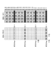
- FIG. 2 is a diagram showing an example of an imaging procedure in the imaging system of FIG. 1;
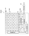
- FIG. 1 is a diagram illustrating an example of a schematic configuration of an imaging device according to a first embodiment of the present disclosure;
- FIG. 2 is a diagram illustrating an example of circuit configurations of sensor pixels and a readout circuit in FIG. 1;
- FIG. It is a figure showing an example of the cross-sectional structure of the sensor pixel of FIG. 4 is a timing chart showing an example of the operation of the imaging device and noise mixing;
- FIG. 1 is a diagram illustrating an example of a schematic configuration of an imaging device according to a first embodiment of the present disclosure
- FIG. 2 is a diagram illustrating an example of circuit configurations of sensor pixels and a readout circuit in FIG. 1
- FIG. 1 is a diagram
- FIG. 4 is a diagram illustrating an example of pixels for which division readout is performed according to the first embodiment of the present disclosure; 4 is a timing chart showing an example of the operation of the imaging device according to the first embodiment of the present disclosure; FIG. 4 is a schematic diagram illustrating an example of interpolation between lines of look-behind signals according to the first embodiment of the present disclosure; It is a figure showing an example of a schematic structure of an imaging device concerning a modification of a 1st embodiment.
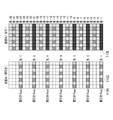
- FIG. 10 is a diagram illustrating an example of pixels for which division readout is performed according to the second embodiment of the present disclosure; 8 is a timing chart showing an example of the operation of the imaging device according to the second embodiment of the present disclosure; FIG.
- FIG. 11 is a diagram illustrating an example of pixels for which division readout is performed according to the third embodiment of the present disclosure
- FIG. 11 is a timing chart showing an example of the operation of an imaging device according to the third embodiment of the present disclosure
- FIG. 11 is a diagram illustrating an example of pixels for which division readout is performed according to the fourth embodiment of the present disclosure
- 1 is a block diagram showing an example of a schematic configuration of a vehicle control system
- FIG. FIG. 4 is an explanatory diagram showing an example of installation positions of an outside information detection unit and an imaging unit;
- an imaging system and an imaging device will be described with reference to the drawings.
- the main components of the imaging system and the imaging device will be mainly described below, the imaging system and the imaging device may have components and functions that are not illustrated or described. The following description does not exclude components or features not shown or described.
- FIG. 1 is a block diagram showing a configuration example of an imaging system 2 including an imaging device 1 according to the first embodiment of the present disclosure.
- the imaging system 2 is, for example, an imaging device such as a digital still camera or a video camera, or an electronic device such as a mobile terminal device such as a smart phone or a tablet terminal.
- the imaging system 2 includes, for example, the imaging device 1, a DSP circuit 210, a frame memory 220, a display section 230, a storage section 240, an operation section 250, and a power supply section 260.
- the DSP circuit 210 corresponds to a specific example of the "signal processing section" of the present disclosure.
- the DSP circuit 210 , frame memory 220 , display section 230 , storage section 240 , operation section 250 and power supply section 260 are interconnected via a bus line 270 .
- the imaging device 1 outputs image data according to incident light.
- the DSP circuit 210 is a signal processing circuit that processes a signal (image data) output from the imaging device 1 .
- the frame memory 220 temporarily holds the image data processed by the DSP circuit 210 on a frame-by-frame basis.
- the display unit 230 is composed of, for example, a panel type display device such as a liquid crystal panel or an organic EL (Electro Luminescence) panel, and displays moving images or still images captured by the imaging device 1 .
- the storage unit 240 records image data of moving images or still images captured by the imaging device 1 in a recording medium such as a semiconductor memory or a hard disk.
- the operation unit 250 issues operation commands for various functions of the imaging system 2 in accordance with user's operations.
- the power source unit 260 appropriately supplies various types of power to the DSP circuit 210, the frame memory 220, the display unit 230, the storage unit 240, and the operation unit 250, to these supply targets.
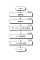
- FIG. 2 shows an example of a flow chart of imaging operations in the imaging system 2 .
- the user instructs to start imaging by operating the operation unit 250 (step S101).
- the operation unit 250 transmits an imaging command to the imaging device 1 (step S102).
- the imaging device 1 (specifically, the system control circuit 24 of the imaging device 1), upon receiving the imaging command, executes imaging with a global shutter operation (step S103).
- the DSP circuit 210 performs predetermined noise reduction processing based on later-described correction data input from the imaging device 1 (step S104). Details of the noise reduction process will be described later with reference to FIGS. 7 to 9.
- the DSP circuit 210 causes the frame memory 220 to hold the image data obtained by the noise reduction process, and the frame memory 220 causes the storage unit 240 to store the image data (step S108). In this manner, imaging in the imaging system 2 is performed.
- the imaging device 1 is, for example, a front side illuminated image sensor such as a CMOS (Complementary Metal Oxide Semiconductor) image sensor.
- the imaging device 1 captures an image by receiving and photoelectrically converting light from a subject to generate an image signal.
- the imaging device 1 outputs pixel signals corresponding to incident light.
- CMOS Complementary Metal Oxide Semiconductor
- a front-illuminated image sensor has a photoelectric conversion unit such as a photodiode that receives light from a subject and converts it into an electrical signal, between the light-receiving surface where the light from the subject is incident and the back surface of the semiconductor substrate. It is an image sensor of the provided configuration. Note that the imaging device 1 may be a back-illuminated image sensor. Also, the present disclosure is not limited to application to CMOS image sensors.
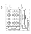
- FIG. 3 shows an example of a schematic configuration of the imaging device 1 according to the first embodiment of the present disclosure.
- the imaging device 1 includes a pixel array section 10 and a logic circuit 20 .
- the pixel array section 10 has a plurality of sensor pixels 11 and a plurality of readout circuits 12 (described later).
- the sensor pixel 11 corresponds to a specific example of "pixel" in the present disclosure.
- Each sensor pixel 11 performs photoelectric conversion and outputs an electric charge according to the amount of received light.
- the plurality of sensor pixels 11 are arranged to face a light receiving surface 10A (described later), and are arranged in a matrix in the pixel array section 10 .
- Each readout circuit 12 outputs a pixel signal based on the charge output from the sensor pixel 11 .
- one readout circuit 12 is provided for each sensor pixel 11 in the pixel array section 10 .
- the plurality of readout circuits 12 may be provided for each of the plurality of sensor pixels 11 in the pixel array
- the pixel array section 10 has a plurality of pixel drive lines HSL and a plurality of data output lines VSL.
- the pixel drive line HSL is a wiring to which a control signal for controlling the output of charges accumulated in the sensor pixels 11 is applied, and extends in the row direction, for example.
- the data output line VSL is a wiring for outputting the pixel signal output from each readout circuit 12 to the logic circuit 20, and extends in the column direction, for example.
- the logic circuit 20 has, for example, a vertical drive circuit 21, a column signal processing circuit 22, a horizontal drive circuit 23 and a system control circuit 24.
- the logic circuit 20 (specifically, the horizontal drive circuit 23) provides image data to the external device by outputting the output voltage for each sensor pixel 11 to the external device.
- the vertical drive circuit 21 sequentially selects a plurality of sensor pixels 11 for each predetermined unit pixel row.
- a "predetermined unit pixel row” refers to a pixel row in which pixels can be selected at the same address. For example, when one sensor pixel 11 is assigned to one readout circuit 12, the "predetermined unit pixel row” refers to one pixel row. Further, for example, when a plurality of sensor pixels 11 share one readout circuit 12, the layout of the plurality of sensor pixels 11 sharing the readout circuit 12 is 2 pixel rows ⁇ n pixel columns (where n is an integer of 1 or more). , the "predetermined unit pixel row" indicates two pixel rows.
- the “predetermined unit pixel row” is 4 pixel rows.
- the vertical drive circuit 21 controls the transistors (eg, transfer transistors TRX, TRG and discharge transistor OFG) in each sensor pixel 11 via the pixel drive line HSL, and further controls the transistors in each readout circuit 12 (eg, reset transistor RST and select transistor SEL).
- the column signal processing circuit 22 performs, for example, correlated double sampling (CDS) processing on pixel signals output from each sensor pixel 11 in a row selected by the vertical driving circuit 21 .
- the column signal processing circuit 22 extracts the signal level of the pixel signal by performing CDS processing, for example, and holds pixel data corresponding to the amount of light received by each sensor pixel 11 .
- the column signal processing circuit 22 has, for example, a column signal processing section for each data output line VSL.
- the column signal processor includes, for example, a single slope A/D converter.
- a single-slope A/D converter includes, for example, a comparator and a counter circuit.
- the horizontal driving circuit 23, for example, sequentially outputs the pixel data held in the column signal processing circuit 22 to the outside.
- the system control circuit 24 controls driving of each block (the vertical drive circuit 21, the column signal processing circuit 22, and the horizontal drive circuit 23) in the logic circuit 20, for example.
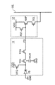
- FIG. 4 shows an example of the circuit configuration of the sensor pixel 11 and the readout circuit 12.
- FIG. FIG. 2 illustrates a case where one sensor pixel 11 is assigned to one readout circuit 12 .
- Each sensor pixel 11 has components in common with each other.
- Each sensor pixel 11 has, for example, a photodiode PD, transfer transistors TRX and TRG, a charge holding portion MEM, a floating diffusion FD, an ejection transistor OFG, and an ejection floating diffusion OFD.
- the transfer transistors TRX, TRG and the discharge transistor OFG are, for example, NMOS (Metal Oxide Semiconductor) transistors.
- the photodiode PD corresponds to a specific example of the "photoelectric conversion unit” of the present disclosure.
- the charge holding portion MEM corresponds to a specific example of the “holding portion” of the present disclosure.
- the readout circuit 12 corresponds to a specific example of the "readout section” of the present disclosure.
- the vertical drive circuit 21 and the horizontal drive circuit 23 correspond to a specific example of the "read control section” of the present disclosure.
- the photodiode PD photoelectrically converts light incident through the light receiving surface 10A (described later).
- the photodiode PD performs photoelectric conversion to generate charges according to the amount of light received.
- the photodiode PD is, for example, a PN junction photoelectric conversion element.
- a cathode of the photodiode PD is electrically connected to the source of the transfer transistor TRX, and an anode of the photodiode PD is electrically connected to a reference potential line (eg ground GND).
- the transfer transistor TRX is connected between the photodiode PD and the transfer transistor TRG, and controls the potential of the charge holding portion MEM according to the control signal applied to the gate of the transfer transistor TRX. For example, when the transfer transistor TRX is turned on, the potential of the charge holding portion MEM deepens. Further, for example, when the transfer transistor TRX is turned off, the potential of the charge holding portion MEM becomes shallow. When the transfer transistor TRX is turned on, the charges accumulated in the photodiode PD are transferred to the charge holding unit MEM via the transfer transistor TRX.
- the drain of the transfer transistor TRX is electrically connected to the source of the transfer transistor TRG, and the gate of the transfer transistor TRX is connected to the pixel drive line HSL.
- the charge holding portion MEM is an impurity semiconductor region that temporarily holds the charge accumulated in the photodiode PD.
- the charge holding unit MEM holds charges transferred from the photodiode PD.
- Both the charge holding portion MEM and the later-described floating diffusion FD are formed of impurity semiconductor regions of a common conductivity type. Furthermore, the impurity concentration of the charge holding portion MEM is lower than that of the floating diffusion FD, which will be described later.
- the transfer transistor TRG is connected between the transfer transistor TRX and the floating diffusion FD, and transfers the charges held in the charge holding unit MEM to the floating diffusion FD according to a control signal applied to the gate of the transfer transistor TRG. transfer to For example, when the transfer transistor TRX is turned off and the transfer transistor TRG is turned on, the charge held in the charge holding unit MEM is transferred to the floating diffusion FD via the transfer transistor TRG.
- a drain of the transfer transistor TRG is electrically connected to the floating diffusion FD, and a gate of the transfer transistor TRG is connected to the pixel drive line HSL.
- the floating diffusion FD is a floating diffusion region (impurity semiconductor region) that temporarily holds charges output from the photodiode PD via the transfer transistor TRX and the transfer transistor TRG.
- a reset transistor RST is connected to the floating diffusion FD, and a vertical signal line VSL is connected via an amplification transistor AMP and a selection transistor SEL.
- the discharge transistor OFG is connected between the photodiode PD and the power supply line VDD, and initializes (resets) the photodiode PD according to a control signal applied to the gate of the discharge transistor OFG. For example, when the discharge transistor OFG is turned on, the potential of the photodiode PD is reset to the potential level of the power supply line VDD. That is, the photodiode PD is initialized. Also, the discharge transistor OFG forms an overflow path between the transfer transistor TRX and the power supply line VDD, for example, and discharges the charges overflowing from the photodiode PD to the power supply line VDD.
- the drain of the discharge transistor OFG is connected to the power supply line VDD, the source of the discharge transistor OFG is connected between the photodiode PD and the transfer transistor TRX, and the gate of the discharge transistor OFG is connected to the pixel drive line HSL. ing.
- the reset transistor RST is connected between the floating diffusion FD and the power supply line VDD, and initializes each region from the charge holding portion MEM to the floating diffusion FD according to a control signal applied to the gate of the reset transistor RST. (reset). For example, when the transfer transistor TRG and the reset transistor RST are turned on, the potentials of the charge holding portion MEM and the floating diffusion FD are reset to the potential level of the power supply line VDD. That is, the charge holding portion MEM and the floating diffusion FD are initialized.
- the drain of the reset transistor RST is connected to the power supply line VDD, the source of the reset transistor RST is connected to the floating diffusion FD, and the gate of the reset transistor RST is connected to the pixel drive line HSL.
- the amplification transistor AMP has a gate connected to the floating diffusion FD, a drain connected to the power supply line VDD, and a source connected to the drain of the select transistor SEL.
- the amplification transistor AMP serves as an input portion of a source follower circuit that reads charges obtained by photoelectric conversion in the photodiode PD. Since the source of the amplification transistor AMP is connected to the vertical signal line VSL through the selection transistor SEL, the amplification transistor AMP constitutes a constant current source connected to one end of the vertical signal line VSL and a source follower circuit.
- the amplification transistor AMP converts the charge obtained by photoelectric conversion in the photodiode PD into a pixel signal, and outputs the pixel signal to the vertical signal line VSL via the selection transistor SEL.
- the selection transistor SEL has a drain connected to the source of the amplification transistor AMP, a source connected to the vertical signal line VSL, and a gate connected to the pixel drive line HSL.
- the selection transistor SEL controls the output of the pixel signal output from the amplification transistor AMP to the vertical signal line VSL according to the control signal applied to the gate of the selection transistor SEL.
- the selection transistor SEL becomes conductive when the control signal is turned on, and the sensor pixel 11 connected to the selection transistor SEL is selected. When the sensor pixel 11 is in the selected state, the pixel signal output from the amplification transistor AMP is read out to the column signal processing circuit 22 via the vertical signal line VSL.
- FIG. 5 shows an example of a cross-sectional configuration of the sensor pixel 11.
- the impurity concentration is indicated by expressions such as "P+”, “N-”, “N+”, and “N++”.
- P+ concentration of the p-type impurity (acceptor) becomes a value higher than the value within the range of 1 ⁇ 10 16 cm ⁇ 3 to 5 ⁇ 10 18 cm ⁇ 3 .
- N+ indicates that the n-type impurity (donor) concentration is higher than "N-”.
- N++ indicates that the n-type impurity (donor) concentration is higher than that of "N+”.
- the n-type impurity (donor) concentration is, for example, a value within the range of 1 ⁇ 10 16 cm -3 to 5 ⁇ 10 18 cm -3 .
- the sensor pixels 11 are formed on a semiconductor substrate 30.
- the semiconductor substrate 30 is, for example, a silicon substrate.
- the semiconductor substrate 30 has a p-well layer 32 on and near the upper surface of the semiconductor substrate 30 and an n-type semiconductor layer 31 at a location deeper than the p-well layer 32 .
- the p-well layer 32 is a p-type semiconductor region formed on the upper surface of the semiconductor substrate 30 and its vicinity.
- An n-type semiconductor region 33 and a p-type semiconductor region 34 are formed in the p-well layer 32 .
- the p-type semiconductor region 34 is formed on the upper surface of the semiconductor substrate 30 and is in contact with the n-type semiconductor region 33 .
- the n-type semiconductor region 33 and the p-type semiconductor region 34 are stacked in the thickness direction (normal direction) of the semiconductor substrate 30 to form a photodiode PD.
- a charge holding portion MEM is formed in a portion of the p-well layer 32 that faces the gate of the transfer transistor TRX.
- the charge holding portion MEM is formed at a predetermined depth from the upper surface of the semiconductor substrate 30 .
- the charge holding portion MEM is composed of an n-type impurity semiconductor region formed in the p-well layer 32 .
- a p-type semiconductor region 35 is formed between the upper surface of the semiconductor substrate 30 and the charge holding portion MEM.
- Both the floating diffusion FD and the discharge floating diffusion OFD are composed of a semiconductor region with a high n-type impurity concentration formed in the p-well layer 32 .
- An exhaust transistor OFG is formed in the vicinity of the exhaust floating diffusion OFD. That is, the sensor pixel 11 has an ejection transistor OFG in the vicinity of the ejection floating diffusion OFD.
- the sensor pixel 11 has a light shielding layer 36 on the semiconductor substrate 30 .
- the light shielding layer 36 has an opening 36A at a position facing the photodiode PD.
- the light receiving surface 10A is exposed in the opening 36A.
- the light shielding layer 36 is arranged around the light receiving surface 10A and at least at a position facing the charge holding portion MEM.
- the light shielding layer 36 is made of, for example, a metal material.
- the charge holding unit MEM holds the charge transferred from the photodiode PD (hereinafter referred to as "signal charge”) as described above.
- signal charge the charge transferred from the photodiode PD
- PLS Physical Light Sensitivity
- blooming dark current
- dark current or the like
- the pixel signal contains a noise component, so that the obtained image has a deteriorated image quality.
- PLS refers to stray light that occurs depending on the amount of incident light when strong light is incident on the photodiode PD. For example, noise charges are generated by light directly entering the charge holding unit MEM and being photoelectrically converted.
- Blooming is, for example, the phenomenon that the photoelectrically converted signal charge exceeds a predetermined level due to the incidence of strong light or the like, and overflows into the charge holding unit MEM. Charges overflowing the photodiode PD normally flow to the discharge floating diffusion OFD. However, it is difficult to completely eliminate the influence of blooming.
- a dark current is a current that flows even when light does not enter a pixel, and is generated, for example, in the charge holding portion MEM.
- FIG. 6 is a timing chart showing an example of the operation of the imaging device 1 and noise contamination.
- FIG. 6 shows readout of a 4-row pixel array section as an example.
- CMOS image sensor having a charge holding portion MEM in each pixel, signal charges for all pixels photoelectrically converted and accumulated in the photodiode PD are transferred to the charge holding portion MEM substantially simultaneously. After that, signals are sequentially read and AD-converted for each pixel row.
- the photodiode PD is reset and exposure is started.
- the exposure period ends, charges are collectively transferred from the photodiode PD to the charge holding unit MEM. Thereby, the signal charge is held in the charge holding portion MEM.
- the reset of the photodiodes PD and the batch transfer of charges to the charge holding unit MEM are performed substantially simultaneously in all rows. Therefore, all pixels are exposed substantially simultaneously (batch exposure).
- the readout period ends when the readout of signals from all rows ends.
- the memory retention period Th indicates a period during which the charge retention unit MEM retains charges from the end of the exposure period until the signal is read out.
- a memory readout period Tr indicates a period during which a signal is read out after the memory retention period Th.
- the imaging device 1 reads out the charge of the charge holding unit MEM by dividing it twice or more in order to grasp the amount of noise charge within the above restrictions and acquire the data necessary for correction. More specifically, the readout control unit, which is the vertical drive circuit 21 and the horizontal drive circuit 23, controls the readout circuit 12 to read out signals from a plurality of pixels so as to generate image data and read out signals during the readout period. Signals are read two or more times from at least some pixels (prefetch pixels).
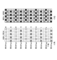
- FIG. 7 is a diagram illustrating an example of pixels for which division readout is performed according to the first embodiment of the present disclosure. Also, the plurality of sensor pixels 11 shown in FIG. 7 are arranged in a matrix. The readout control unit reads out signals from the pixels on a row-by-row basis. As an example, the color filters of each pixel shown in FIG. 7 are arranged in a Bayer array.
- FIG. 7 shows an example of double reading by the reading control unit. These two divided readouts are defined as prefetch and postfetch. Also, a line read during prefetching is defined as a "prefetching line”.
- pixels in the pre-read rows are pixels thinned out at predetermined row intervals from the arrayed pixels. That is, the read control unit pre-reads pixels so as to thin out the pixels.
- the charge holding units MEM of the pre-reading rows are reset (initialized), and the charges in the charge holding units MEM are emptied.
- the once reset charge holding unit MEM accumulates noise charges due to PLS, blooming, and dark current before backward reading.
- the charge holding portions MEM of the rows that were not read during the pre-reading are read, and the charge holding portions MEM of the pre-reading rows (post-1, post-8, post-15, post-22 in FIG. 7) are read. A second reading is performed.
- the lines that were not read during pre-reading are the lines other than the pre-read lines (after-2 to after-7, after-9 to after-14, after-16 to after-21, after-23 to after-23 in FIG. 7). -28). That is, in post-reading, readout of the charge holding units MEM for all pixels (all rows) is performed. During this post-reading, the signals obtained by reading the charge holding portions MEM of the pre-reading rows (post-1, post-8, post-15, post-22 in FIG. 7) read during pre-reading are PLS , are the signals of the blooming and dark current components.
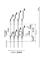
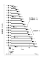
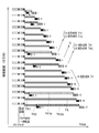
- FIG. 8 is a timing chart showing an example of the operation of the imaging device 1 according to the first embodiment of the present disclosure.
- FIG. 8 shows the memory retention period and read timing for each row. Note that FIG. 8 shows an example of readout of pixels from the bottom to the 17th row in FIG.
- the read-ahead reads out the read-ahead rows (first-1, first-2, and first-3 in FIG. 8). Reading is performed in the order of first-1, first-2 and first-3. As a result, the read-ahead signal S1 for the memory retention period Th1 is obtained.
- lookbehind is performed. Lookbehind is performed on all pixel rows. Reading is performed in the order of after-1, after-2, after-3, . . . , after-15, after-16, after-17. As described above, the pre-reading resets the charge in the charge holding portion MEM of the pre-reading row. Therefore, the read-back signal S3 of the memory retention period Th1a is obtained by reading the read-ahead rows (after-1, after-8, and after-15 in FIG. 8). Note that the memory holding period Th1a is a memory holding period from pre-reading to post-reading in a certain pixel row.
- the readout control unit reads the charge held in the charge holding unit MEM during the period from the initialization of the charge holding unit MEM to the readout of the next signal as a signal that is read the second time or later during the readout period. .
- the post-read signal S2 of the memory holding period Th is obtained.
- the read-ahead signal S1 of the read-ahead row is a pixel signal superimposed with a slight noise component because the memory holding period Th1 is short.
- the post-reading signal S3 of the pre-reading row is a signal due to noise charges accumulated during the memory retention period Th1a.
- the look-behind signal S2 for rows other than the look-ahead row is a pixel signal superimposed with a signal due to noise charges accumulated during the memory retention period Th.
- the look-behind signal S3 is a signal due to noise charges, as described above.
- This post-reading signal S3 is data for correcting (suppressing) noise.
- FIG. 9 is a schematic diagram illustrating an example of interpolation between lines of the look-behind signal S3 according to the first embodiment of the present disclosure.
- FIG. 9 shows the distribution of noise by PLS as an example.
- the imaging system 2 when capturing a moving strong light, a part of the periphery of the strong light in the image becomes brighter than it should be. This is because the noise charge due to PLS is large.
- the imaging system 2 for example, suppresses the influence of such noise charges.
- a noise charge signal distribution for all pixels is created by general interpolation processing of the signal between lines.
- the interpolation processing is, for example, linear interpolation or the like, but is not limited to this.
- This interpolated signal for all pixels is assumed to be a distribution signal S3a shown in FIG.
- PLS brightens the central portion of the distribution signal S3a.
- Noise correction processing of the image data is performed using this distribution signal S3a. Creation of the noise charge signal distribution and noise correction processing are created by the DSP circuit 210 shown in FIG. 1, for example.
- the memory retention period Th1 is shorter than the memory retention period Th, and a look-ahead signal S1 in which the influence of noise such as PLS is suppressed is obtained.
- a look-ahead signal S1 in which the influence of noise such as PLS is suppressed is obtained.
- the readout control unit reads out signals twice from the pixels in the pre-reading rows, which are part of the pixels, during the readout period. First, the signals of the pixels in the pre-reading row are read out, and then the signals of the pixels in all rows are read out. Thereby, in the pre-reading row, pixel signals with less noise charges can be obtained by pre-reading. Furthermore, the look-behind makes it possible to obtain a noise charge signal that is used for noise correction processing. A noise charge signal distribution for all pixels can be created by interpolation from noise charge signals obtained by post-reading, and the influence of noise charges in rows other than pre-reading rows can be subtracted. As a result, it is possible to obtain image data in which noise charges are suppressed.
- the look-ahead signal S1 may be slightly affected by noise charges.
- noise correction processing is not performed on the look-ahead signal S1. Therefore, for example, the drive capability of the scanning lines (the vertical drive circuit 21 and the horizontal drive circuit 23) is increased only during pre-reading, or the current of the readout circuit 12 (for example, the constant current source connected to the vertical signal line VSL) is increased.
- the time required for prefetching can be further shortened by, for example, As a result, the memory retention period Th1 can be further shortened, and the influence of noise charges on the preread signal S1 can be further suppressed.
- the readout control unit reads out the signals from all the pixels at the second speed, which is slower than the first speed.
- the read-behind read speed is unchanged and slower than the read-ahead read speed. As a result, the influence such as an increase in power consumption is small.
- signal reading is performed row by row.
- signals are not limited to this, and signals may be sequentially read out in units of columns or in units of pixels.
- pixels are read ahead on a row-by-row basis.
- the read control unit is not limited to this, and the read-ahead may be performed on a column-by-column basis.
- the column signal processing circuit 22 is used for AD conversion. That is, one AD converter is shared by the pixels in the pixel column. However, an AD converter may be arranged for each sensor pixel 11 . Even when AD conversion and signal readout are performed for each pixel, the embodiments of the present disclosure can be applied if, for example, the timing of charge transfer is shifted for each pixel.
- the signal is read out a maximum of two times during the readout period, but it may be read out three times or more.
- the second and subsequent readouts during the readout period are used for noise correction processing.
- an FPGA Field-Programmable Gate Array
- an FPGA may create the noise charge signal distribution and perform the noise correction processing.
- the charge holding unit MEM may be replaced by a floating diffusion FD.
- a capacitor having an MIM (Metal Insulator Metal) structure is provided in the voltage domain global shutter pixel.
- the charge generated by the photodiode PD is converted into a voltage and held in this capacitor. Therefore, instead of the charge holding unit MEM, a voltage holding unit that holds, as a voltage, information on the charge photoelectrically converted by the photodiode PD may be used. In this manner, the holding unit may hold information about electric charge, not limited to electric charge.
- a pixel dedicated to correction or a charge holding section (memory) dedicated to correction separate from the charge holding section MEM is arranged in the pixel array section 10.
- the reduction in pixel area may lead to a reduction in the saturation signal amount, a reduction in sensitivity, or a deterioration in resolution.
- pixels dedicated to correction or charge holding portions dedicated to correction are not provided. Therefore, data for correcting noise due to PLS, blooming, dark current, etc. can be acquired by driving without changing the configuration of the imaging device 1 . As a result, it is possible to acquire data for correcting noise while suppressing deterioration of characteristics due to reduction in pixel area.
- FIG. 10 shows an example of a schematic configuration of an imaging device 1 according to a modification of the first embodiment.
- the modified example of the first embodiment differs from the first embodiment in that the imaging apparatus 1 performs noise correction processing.
- the imaging device 1 reads and AD-converts the look-behind signal S3, which is correction data, and outputs the look-behind signal S3 to the outside (for example, the DSP circuit 210).
- the DSP circuit 210 creates a noise charge signal distribution and performs noise correction processing based on the look-behind signal S3.
- the imaging device 1 according to the second embodiment further includes a signal processing section 25 .
- the signal processing unit 25 has, for example, the functions of the DSP circuit 210 described in the first embodiment. That is, the signal processing unit 25 creates a noise charge signal distribution and performs noise correction processing based on the look-behind signal S3. Thus, the signal processing unit 25 processes signals for generating image data.
- the signal processing unit 25 has, for example, a frame buffer or frame memory. In the second embodiment, the imaging device 1 can independently perform noise correction processing.
- the signal processing section 25 is connected to the horizontal drive circuit 23 .
- the signal processing section 25 may be connected to the column signal processing circuit 22 or arranged in the column signal processing circuit 22, for example.
- the signal processing unit 25 may be arranged on the same substrate as the imaging device 1 .
- the signal processing section 25 is arranged on a substrate on which a circuit for signal processing is arranged, which is different from the substrate on which the pixel array section 10 is arranged.
- a signal processing unit 25 that performs noise correction processing may be provided in the imaging device 1 as in the modification of the first embodiment. Also in this case, the same effect as in the first embodiment can be obtained.
- FIG. 11 is a diagram illustrating an example of pixels for which division readout is performed according to the second embodiment of the present disclosure.
- the second embodiment differs from the first embodiment in the look-ahead thinning rate.
- the number of prefetch lines (first-1 to first-7 in FIG. 11) is larger than in FIG. 7 of the first embodiment.
- prefetching is performed every 7 lines
- prefetching is performed every 4 lines. That is, compared to FIG. 7 of the first embodiment, the prefetch line thinning rate is reduced and the interval between prefetch lines is narrowed. As a result, the resolution of pixels in the pre-read row can be improved. As a result, the noise charge signal distribution can be created with higher accuracy, and the correction accuracy can be improved.
- FIG. 12 is a timing chart showing an example of the operation of the imaging device 1 according to the second embodiment of the present disclosure.
- the memory retention period Th1 of the row whose reading order is later becomes longer, even if it is a pre-read row. Therefore, the influence of noise charges superimposed on the look-ahead signal S1 may increase. In this case, it becomes difficult to suppress the influence of the noise charges of the pixels in the preread rows in the combined image data. Therefore, regarding the change of the thinning rate, there is a trade-off relationship between the correction accuracy of lines other than the prefetch lines and the magnitude of the noise component of the prefetch lines.
- the pre-reading line thinning rate is set according to the performance required for the imaging apparatus 1 .
- the thinning rate of prefetch lines may be changed as in the second embodiment. Also in this case, the same effect as in the first embodiment can be obtained. Note that the imaging system 2 and the imaging device 1 according to the second embodiment may be combined with the modified example of the first embodiment.
- FIG. 13 is a diagram illustrating an example of pixels for which division readout is performed according to the third embodiment of the present disclosure.
- the third embodiment differs from the first embodiment in that readout is performed three times by line thinning.
- middle reading is performed between look-ahead and look-behind, as compared with the first embodiment. It should be noted that mid-reading corresponds to performing prefetching multiple times (for example, twice) by dividing prefetch lines. Also, a line that is read during middle reading is defined as a "middle reading line".
- the signals of the middle reading rows (-1 to middle-4 in FIG. 13) are read.
- the thinning rate of mid-reading lines is, for example, the same as the thinning rate of prefetching lines.
- the middle reading line is shifted from the lookahead line by two lines, for example.
- the charge holding units MEM of the middle readout rows are reset and the charges in the charge holding units MEM are emptied as in the pre-reading. Become.
- the once reset charge holding unit MEM accumulates noise charges due to PLS, blooming, and dark current before backward reading.
- FIG. 14 is a timing chart showing an example of the operation of the imaging device 1 according to the third embodiment of the present disclosure.
- intermediate reading is performed between the look-ahead and look-behind described in FIG. 8 of the first embodiment.
- the middle reading rows (-1, middle-2, and middle-3 in FIG. 14) are read. Reading is performed in the order of middle-1, middle-2, and middle-3.
- the intermediate reading signal S4 for the memory holding period Th2 is obtained.
- the backward reading signal S5 of the memory holding period Th2a is obtained by reading the intermediate reading rows (the backward-3, backward-10, backward-17 in FIG. 14).
- the middle reading signal S4 for the middle reading row is a pixel signal superimposed with a slight noise component because the memory retention period Th2 is short.
- the post-reading signal S5 for the intermediate reading row is a signal due to noise charges accumulated during the memory retention period Th2a.
- a photo for all pixels (all rows) is obtained.
- a signal photoelectrically converted by the diode PD is obtained.
- the look-behind signals S3 and S5 are signals due to noise charges as described above. These post-reading signals S3 and S5 are one of data for correcting noise.
- the look-behind signal S5 can improve the resolution of the noise charge signal compared to the first embodiment. As a result, the noise charge signal distribution can be created with higher accuracy, and the correction accuracy can be improved.
- the memory holding period Th2 of the intermediate reading signal S4 is longer than the memory holding period Th1 of the prefetching signal S1. Therefore, the mid-reading signal S4 may be more influenced by superimposed noise charges than the pre-reading signal S1. In this case, it becomes difficult to suppress the influence of the noise charge on the middle reading line in the synthesized image data. Therefore, in substantially the same manner as the change in the prefetch row thinning rate described in the second embodiment, regarding the change in the number of times of readout, the There is a trade-off relationship with the size of the noise component.
- reading may be performed three times or more, instead of being limited to two times. Also in this case, the same effect as in the first embodiment can be obtained. Note that the imaging system 2 and the imaging device 1 according to the third embodiment may be combined with the modified example of the first embodiment and the second embodiment.
- FIG. 15 is a diagram illustrating an example of pixels for which division readout is performed according to the fourth embodiment of the present disclosure.
- the fourth embodiment differs from the first embodiment in that prefetching of pixels is not performed in units of rows.
- prefetching is performed pixel by pixel instead of line by line. That is, the read control unit performs pre-reading on a pixel-by-pixel basis.
- the look-ahead pixels are randomly arranged in the pixel array section 10 .
- the look-ahead pixels are red pixels 11R on the 1st, 7th, 13th, 19th and 25th rows from the bottom and blue pixels 11R on the 4th, 10th, 16th, 22nd and 28th rows from the bottom. This is pixel 11B. In this way, thinning out pixels by pixel instead of by rows increases the accuracy of noise correction, and may enable high-speed scanning during pre-reading.
- Prefetching may be performed for each pixel as in the fourth embodiment. Also in this case, the same effect as in the first embodiment can be obtained.
- the imaging system 2 and imaging device 1 according to the fourth embodiment may be combined with the modification of the first embodiment, and the second and third embodiments.
- the technology (the present technology) according to the present disclosure can be applied to various products.
- the technology according to the present disclosure can be realized as a device mounted on any type of moving body such as automobiles, electric vehicles, hybrid electric vehicles, motorcycles, bicycles, personal mobility, airplanes, drones, ships, and robots. may
- FIG. 16 is a block diagram showing a schematic configuration example of a vehicle control system, which is an example of a mobile control system to which the technology according to the present disclosure can be applied.
- a vehicle control system 12000 includes a plurality of electronic control units connected via a communication network 12001.
- the vehicle control system 12000 includes a drive system control unit 12010, a body system control unit 12020, an exterior information detection unit 12030, an interior information detection unit 12040, and an integrated control unit 12050.
- a microcomputer 12051, an audio/image output unit 12052, and an in-vehicle network I/F (interface) 12053 are illustrated.
- the drive system control unit 12010 controls the operation of devices related to the drive system of the vehicle according to various programs.
- the driving system control unit 12010 includes a driving force generator for generating driving force of the vehicle such as an internal combustion engine or a driving motor, a driving force transmission mechanism for transmitting the driving force to the wheels, and a steering angle of the vehicle. It functions as a control device such as a steering mechanism to adjust and a brake device to generate braking force of the vehicle.
- the body system control unit 12020 controls the operation of various devices equipped on the vehicle body according to various programs.
- the body system control unit 12020 functions as a keyless entry system, a smart key system, a power window device, or a control device for various lamps such as headlamps, back lamps, brake lamps, winkers or fog lamps.
- the body system control unit 12020 can receive radio waves transmitted from a portable device that substitutes for a key or signals from various switches.
- the body system control unit 12020 receives the input of these radio waves or signals and controls the door lock device, power window device, lamps, etc. of the vehicle.
- the vehicle exterior information detection unit 12030 detects information outside the vehicle in which the vehicle control system 12000 is installed.
- the vehicle exterior information detection unit 12030 is connected with an imaging section 12031 .
- the vehicle exterior information detection unit 12030 causes the imaging unit 12031 to capture an image of the exterior of the vehicle, and receives the captured image.
- the vehicle exterior information detection unit 12030 may perform object detection processing or distance detection processing such as people, vehicles, obstacles, signs, or characters on the road surface based on the received image.
- the imaging unit 12031 is an optical sensor that receives light and outputs an electrical signal according to the amount of received light.
- the imaging unit 12031 can output the electric signal as an image, and can also output it as distance measurement information.
- the light received by the imaging unit 12031 may be visible light or non-visible light such as infrared rays.
- the in-vehicle information detection unit 12040 detects in-vehicle information.
- the in-vehicle information detection unit 12040 is connected to, for example, a driver state detection section 12041 that detects the state of the driver.
- the driver state detection unit 12041 includes, for example, a camera that captures an image of the driver, and the in-vehicle information detection unit 12040 detects the degree of fatigue or concentration of the driver based on the detection information input from the driver state detection unit 12041. It may be calculated, or it may be determined whether the driver is dozing off.
- the microcomputer 12051 calculates control target values for the driving force generator, the steering mechanism, or the braking device based on the information inside and outside the vehicle acquired by the vehicle exterior information detection unit 12030 or the vehicle interior information detection unit 12040, and controls the drive system control unit.
- a control command can be output to 12010 .
- the microcomputer 12051 realizes the functions of ADAS (Advanced Driver Assistance System) including collision avoidance or shock mitigation, follow-up driving based on inter-vehicle distance, vehicle speed maintenance driving, vehicle collision warning, or vehicle lane deviation warning. Cooperative control can be performed for the purpose of ADAS (Advanced Driver Assistance System) including collision avoidance or shock mitigation, follow-up driving based on inter-vehicle distance, vehicle speed maintenance driving, vehicle collision warning, or vehicle lane deviation warning. Cooperative control can be performed for the purpose of ADAS (Advanced Driver Assistance System) including collision avoidance or shock mitigation, follow-up driving based on inter-vehicle distance, vehicle speed maintenance driving, vehicle collision warning, or vehicle
- the microcomputer 12051 controls the driving force generator, the steering mechanism, the braking device, etc. based on the information about the vehicle surroundings acquired by the vehicle exterior information detection unit 12030 or the vehicle interior information detection unit 12040, so that the driver's Cooperative control can be performed for the purpose of autonomous driving, etc., in which vehicles autonomously travel without depending on operation.
- the microcomputer 12051 can output a control command to the body system control unit 12020 based on the information outside the vehicle acquired by the information detection unit 12030 outside the vehicle.
- the microcomputer 12051 controls the headlamps according to the position of the preceding vehicle or the oncoming vehicle detected by the vehicle exterior information detection unit 12030, and performs cooperative control aimed at anti-glare such as switching from high beam to low beam. It can be carried out.
- the audio/image output unit 12052 transmits at least one of audio and/or image output signals to an output device capable of visually or audibly notifying the passengers of the vehicle or the outside of the vehicle.
- an audio speaker 12061, a display unit 12062, and an instrument panel 12063 are illustrated as output devices.
- the display unit 12062 may include at least one of an on-board display and a head-up display, for example.
- FIG. 17 is a diagram showing an example of the installation position of the imaging unit 12031.
- the vehicle 12100 has imaging units 12101, 12102, 12103, 12104, and 12105 as the imaging unit 12031.
- the imaging units 12101, 12102, 12103, 12104, and 12105 are provided at positions such as the front nose of the vehicle 12100, the side mirrors, the rear bumper, the back door, and the upper part of the windshield in the vehicle interior, for example.
- An image pickup unit 12101 provided in the front nose and an image pickup unit 12105 provided above the windshield in the passenger compartment mainly acquire images in front of the vehicle 12100 .
- Imaging units 12102 and 12103 provided in the side mirrors mainly acquire side images of the vehicle 12100 .
- An imaging unit 12104 provided in the rear bumper or back door mainly acquires an image behind the vehicle 12100 .
- Forward images acquired by the imaging units 12101 and 12105 are mainly used for detecting preceding vehicles, pedestrians, obstacles, traffic lights, traffic signs, lanes, and the like.
- FIG. 17 shows an example of the imaging range of the imaging units 12101 to 12104.
- the imaging range 12111 indicates the imaging range of the imaging unit 12101 provided in the front nose
- the imaging ranges 12112 and 12113 indicate the imaging ranges of the imaging units 12102 and 12103 provided in the side mirrors, respectively
- the imaging range 12114 The imaging range of an imaging unit 12104 provided on the rear bumper or back door is shown. For example, by superimposing the image data captured by the imaging units 12101 to 12104, a bird's-eye view image of the vehicle 12100 viewed from above can be obtained.
- At least one of the imaging units 12101 to 12104 may have a function of acquiring distance information.
- at least one of the imaging units 12101 to 12104 may be a stereo camera composed of a plurality of imaging elements, or may be an imaging element having pixels for phase difference detection.
- the microcomputer 12051 determines the distance to each three-dimensional object within the imaging ranges 12111 to 12114 and changes in this distance over time (relative velocity with respect to the vehicle 12100). , it is possible to extract, as the preceding vehicle, the closest three-dimensional object on the course of the vehicle 12100, which runs at a predetermined speed (for example, 0 km/h or more) in substantially the same direction as the vehicle 12100. can. Furthermore, the microcomputer 12051 can set the inter-vehicle distance to be secured in advance in front of the preceding vehicle, and perform automatic brake control (including following stop control) and automatic acceleration control (including following start control). In this way, cooperative control can be performed for the purpose of automatic driving in which the vehicle runs autonomously without relying on the operation of the driver.
- automatic brake control including following stop control
- automatic acceleration control including following start control
- the microcomputer 12051 converts three-dimensional object data related to three-dimensional objects to other three-dimensional objects such as motorcycles, ordinary vehicles, large vehicles, pedestrians, and utility poles. It can be classified and extracted and used for automatic avoidance of obstacles. For example, the microcomputer 12051 distinguishes obstacles around the vehicle 12100 into those that are visible to the driver of the vehicle 12100 and those that are difficult to see. Then, the microcomputer 12051 judges the collision risk indicating the degree of danger of collision with each obstacle, and when the collision risk is equal to or higher than the set value and there is a possibility of collision, an audio speaker 12061 and a display unit 12062 are displayed. By outputting an alarm to the driver via the drive system control unit 12010 and performing forced deceleration and avoidance steering via the drive system control unit 12010, driving support for collision avoidance can be performed.
- At least one of the imaging units 12101 to 12104 may be an infrared camera that detects infrared rays.
- the microcomputer 12051 can recognize a pedestrian by determining whether or not the pedestrian exists in the captured images of the imaging units 12101 to 12104 .
- recognition of a pedestrian is performed by, for example, a procedure for extracting feature points in images captured by the imaging units 12101 to 12104 as infrared cameras, and performing pattern matching processing on a series of feature points indicating the outline of an object to determine whether or not the pedestrian is a pedestrian.
- the audio image output unit 12052 outputs a rectangular outline for emphasis to the recognized pedestrian. is superimposed on the display unit 12062 . Also, the audio/image output unit 12052 may control the display unit 12062 to display an icon or the like indicating a pedestrian at a desired position.
- the technology according to the present disclosure can be applied to, for example, the imaging units 12031, 12101, 12102, 12103, 12104, and 12105, the driver state detection unit 12041, and the like among the configurations described above.
- the imaging system 2 and the imaging device 1 of the present disclosure can be applied to these imaging units and detection units. Then, by applying the technology according to the present disclosure, it is possible to suppress noise, so it is possible to realize safer vehicle travel.
- this technique can take the following structures. (1) a reading unit that reads out the charge or the information as a signal from a plurality of pixels having a photoelectric conversion unit and a holding unit that holds the photoelectrically converted charge or information about the charge; a readout control unit that reads out signals from the plurality of pixels so as to generate image data by controlling the readout unit and reads signals from at least some of the pixels twice or more during a readout period; and a signal processing unit that processes a signal for generating the image data based on a signal read out for a second time or later during a readout period.
- the readout control unit converts the charge or the information held in the holding unit during the period from the initialization of the holding unit to the readout of the next signal as a signal to be read out for the second and subsequent times during the readout period.
- the imaging system according to (1) which reads out.
- the readout control unit reads signals from at least some of the pixels two or more times during a readout period by reading signals from all of the pixels after reading out signals from at least some of the pixels;
- the readout control unit read out signals from at least some of the pixels a plurality of times by dividing at least some of the pixels, and then reading the signals from all the pixels, thereby reading the signals from at least some of the pixels twice during the readout period.
- the imaging system according to (3) read out at least once.
- the readout control unit reads signals from at least some of the pixels at a first speed and then reads signals from all the pixels at a second speed slower than the first speed;
- the imaging system according to (4) The imaging system according to (4).
- the plurality of pixels are arranged in a matrix;
- the readout control unit reads signals from at least some of the thinned pixels twice or more during a readout period;
- the signal processing unit is generating a signal distribution by interpolating the signals between the thinned pixels based on the signals read out for the second and subsequent times during the readout period;
- the imaging system according to any one of (1) to (7), wherein the signal for generating the image data is processed based on the signal distribution.
- the signal processing unit subtracts the signals of the corresponding pixels based on the signal distribution from the signals read from the pixels other than at least some of the thinned-out pixels, thereby obtaining the image (8)
- the imaging system of (8) which processes the signal to generate the data.
- Imaging device 1 imaging device, 2 imaging system, 10 pixel array section, 11 sensor pixel, 12 readout circuit, 20 logic circuit, 21 vertical drive circuit, 22 column signal processing circuit, 23 horizontal drive circuit, 25 signal processing section, 210 DSP circuit, PD photodiode, MEM charge holding unit, S1 look-ahead signal, S2 look-ahead signal, S3 look-ahead signal, S3a distribution signal, S4 mid-read signal, S5 look-ahead signal
Landscapes
- Engineering & Computer Science (AREA)
- Multimedia (AREA)
- Signal Processing (AREA)
- Transforming Light Signals Into Electric Signals (AREA)
Abstract
[課題]信号のノイズ成分を抑制するためのデータを取得する。 [解決手段]撮像システムは、光電変換部と、光電変換された電荷又は前記電荷に関する情報を保持する保持部と、を有する複数の画素から、前記電荷又は前記情報を信号として読み出す読出部と、前記読出部を制御することにより、画像データを生成するように複数の前記画素から信号を読み出すとともに、読出期間中に少なくとも一部の前記画素から信号を2回以上読み出す読出制御部と、読出期間中に2回目以降に読み出された信号に基づいて、前記画像データを生成するための信号を処理する信号処理部と、を備える。
Description
本開示による実施形態は、撮像システム及び撮像装置に関する。
画素内にメモリを有するグローバルシャッタ方式のイメージセンサにおいて、メモリへの光漏れ起因のPLS(Parasitic Light Sensitivity)、及び、フォトダイオードからの信号漏れ(ブルーミング)等が問題となる。このPLS及びブルーミング等によって、メモリに保持された信号電荷にノイズ成分が重畳されてしまう。このノイズ成分を補正するために、補正専用の画素、又は、補正専用のメモリを画素アレイ内に配置することが考えられている(特許文献1参照)。
しかしながら、画素アレイ内に補正専用の画素又は補正専用のメモリを配置すると、画素面積の低下により、飽和信号量の低下、感度の低下、又は、解像度の悪化につながる場合がある。
そこで、本開示では、信号のノイズ成分を抑制するためのデータを取得することができる撮像装置システム及び撮像装置を提供するものである。
上記の課題を解決するために、本開示によれば、
光電変換部と、光電変換された電荷又は前記電荷に関する情報を保持する保持部と、を有する複数の画素から、前記電荷又は前記情報を信号として読み出す読出部と、
前記読出部を制御することにより、画像データを生成するように複数の前記画素から信号を読み出すとともに、読出期間中に少なくとも一部の前記画素から信号を2回以上読み出す読出制御部と、
読出期間中に2回目以降に読み出された信号に基づいて、前記画像データを生成するための信号を処理する信号処理部と、を備える、撮像システムが提供される。
光電変換部と、光電変換された電荷又は前記電荷に関する情報を保持する保持部と、を有する複数の画素から、前記電荷又は前記情報を信号として読み出す読出部と、
前記読出部を制御することにより、画像データを生成するように複数の前記画素から信号を読み出すとともに、読出期間中に少なくとも一部の前記画素から信号を2回以上読み出す読出制御部と、
読出期間中に2回目以降に読み出された信号に基づいて、前記画像データを生成するための信号を処理する信号処理部と、を備える、撮像システムが提供される。
信号が読み出された少なくとも一部の前記画素の前記保持部は、初期化され、
前記読出制御部は、前記保持部が初期化されてから次の信号の読み出しまでの期間に前記保持部に保持された前記電荷又は前記情報を、読出期間中に2回目以降に読み出される信号として読み出してもよい。
前記読出制御部は、前記保持部が初期化されてから次の信号の読み出しまでの期間に前記保持部に保持された前記電荷又は前記情報を、読出期間中に2回目以降に読み出される信号として読み出してもよい。
前記読出制御部は、少なくとも一部の前記画素から信号を読み出した後に全ての前記画素から信号を読み出すことにより、読出期間中に少なくとも一部の前記画素から信号を2回以上読み出してもよい。
前記読出制御部は、少なくとも一部の前記画素を分けて信号を複数回読み出した後に全ての前記画素から信号を読み出すことにより、読出期間中に少なくとも一部の前記画素から信号を2回以上読み出してもよい。
前記読出制御部は、第1速度で少なくとも一部の前記画素から信号を読み出した後に、前記第1速度よりも遅い第2速度で全ての前記画素から信号を読み出してもよい。
複数の前記画素は、行列状に配置され、
前記読出制御部は、行単位又は列単位で少なくとも一部の前記画素から信号を読み出した後に、全ての前記画素から信号を読み出してもよい。
前記読出制御部は、行単位又は列単位で少なくとも一部の前記画素から信号を読み出した後に、全ての前記画素から信号を読み出してもよい。
前記読出制御部は、前記画素単位で少なくとも一部の前記画素から信号を読み出した後に、全ての前記画素から信号を読み出してもよい。
前記読出制御部は、読出期間中に、間引かれた少なくとも一部の前記画素から信号を2回以上読み出し、
前記信号処理部は、
読出期間中に2回目以降に読み出された信号に基づいて、間引かれた前記画素の間の信号を補間することにより、信号分布を生成し、
前記信号分布に基づいて、前記画像データを生成するための信号を処理してもよい。
前記信号処理部は、
読出期間中に2回目以降に読み出された信号に基づいて、間引かれた前記画素の間の信号を補間することにより、信号分布を生成し、
前記信号分布に基づいて、前記画像データを生成するための信号を処理してもよい。
前記信号処理部は、間引かれた少なくとも一部の前記画素以外の前記画素から読み出された信号から、前記信号分布に基づく対応する前記画素の信号を減算することにより、前記画像データを生成するための信号を処理してもよい。
前記読出制御部は、複数の前記画素ごとに、又は、1つの前記画素ごとに、順次信号を読み出してもよい。
全ての前記画素は、略同時に露光され、
露光の終了後、全ての前記画素の前記電荷又は前記情報は、略同時に前記保持部に保持されてもよい。
露光の終了後、全ての前記画素の前記電荷又は前記情報は、略同時に前記保持部に保持されてもよい。
本開示によれば、光電変換部と、光電変換された電荷又は前記電荷に関する情報を保持する保持部と、を有する複数の画素から、前記電荷又は前記情報を信号として読み出す読出部と、
前記読出部を制御することにより、画像データを生成するように複数の前記画素から信号を読み出すとともに、読出期間中に少なくとも一部の前記画素から信号を2回以上読み出す読出制御部と、を備える、撮像装置が提供される。
前記読出部を制御することにより、画像データを生成するように複数の前記画素から信号を読み出すとともに、読出期間中に少なくとも一部の前記画素から信号を2回以上読み出す読出制御部と、を備える、撮像装置が提供される。
以下、図面を参照して、撮像システム及び撮像装置の実施形態について説明する。以下では、撮像システム及び撮像装置の主要な構成部分を中心に説明するが、撮像システム及び撮像装置には、図示又は説明されていない構成部分や機能が存在しうる。以下の説明は、図示又は説明されていない構成部分や機能を除外するものではない。
<第1の実施の形態>
[撮像システム]
図1は、本開示の第1の実施の形態に係る撮像装置1を備えた撮像システム2の構成例を示すブロック図である。
[撮像システム]
図1は、本開示の第1の実施の形態に係る撮像装置1を備えた撮像システム2の構成例を示すブロック図である。
撮像システム2は、例えば、デジタルスチルカメラやビデオカメラ等の撮像装置や、スマートフォンやタブレット型端末等の携帯端末装置などの電子機器である。撮像システム2は、例えば、撮像装置1、DSP回路210、フレームメモリ220、表示部230、記憶部240、操作部250及び電源部260を備えている。DSP回路210が、本開示の「信号処理部」の一具体例に相当する。撮像システム2において、DSP回路210、フレームメモリ220、表示部230、記憶部240、操作部250及び電源部260は、バスライン270を介して相互に接続されている。
撮像装置1は、入射光に応じた画像データを出力する。DSP回路210は、撮像装置1から出力される信号(画像データ)を処理する信号処理回路である。フレームメモリ220は、DSP回路210により処理された画像データを、フレーム単位で一時的に保持する。表示部230は、例えば、液晶パネルや有機EL(Electro Luminescence)パネル等のパネル型表示装置からなり、撮像装置1で撮像された動画又は静止画を表示する。記憶部240は、撮像装置1で撮像された動画又は静止画の画像データを、半導体メモリやハードディスク等の記録媒体に記録する。操作部250は、ユーザによる操作に従い、撮像システム2が有する各種の機能についての操作指令を発する。電源部260は、DSP回路210、フレームメモリ220、表示部230、記憶部240及び操作部250の動作電源となる各種の電源を、これら供給対象に対して適宜供給する。
次に、撮像システム2における撮像手順について説明する。
図2は、撮像システム2における撮像動作のフローチャートの一例を表す。ユーザは、操作部250を操作することにより撮像開始を指示する(ステップS101)。すると、操作部250は、撮像指令を撮像装置1に送信する(ステップS102)。撮像装置1(具体的には撮像装置1のシステム制御回路24)は、撮像指令を受けると、グローバルシャッター動作での撮像を実行する(ステップS103)。DSP回路210は、撮像装置1から入力された後述の補正用データに基づいて所定のノイズ低減処理を行う(ステップS104)。なお、ノイズ低減処理の詳細については、図7~図9を参照して、後で説明する。DSP回路210は、ノイズ低減処理により得られた画像データをフレームメモリ220に保持させ、フレームメモリ220は、画像データを記憶部240に記憶させる(ステップS108)。このようにして、撮像システム2における撮像が行われる。
[撮像装置の構成]
本開示の第1の実施の形態に係る撮像装置1について説明する。撮像装置1は、例えば、CMOS(Complementary Metal Oxide Semiconductor)イメージセンサ等からなる表面照射型のイメージセンサである。撮像装置1は、被写体からの光を受光して光電変換し、画像信号を生成することで画像を撮像する。撮像装置1は、入射光に応じた画素信号を出力する。
本開示の第1の実施の形態に係る撮像装置1について説明する。撮像装置1は、例えば、CMOS(Complementary Metal Oxide Semiconductor)イメージセンサ等からなる表面照射型のイメージセンサである。撮像装置1は、被写体からの光を受光して光電変換し、画像信号を生成することで画像を撮像する。撮像装置1は、入射光に応じた画素信号を出力する。
表面照射型のイメージセンサとは、被写体からの光が入射する受光面と、半導体基板の裏面との間に、被写体からの光を受光し、電気信号に変換するフォトダイオード等の光電変換部が設けられている構成のイメージセンサである。なお、撮像装置1は、裏面照射型のイメージセンサであってもよい。また、本開示は、CMOSイメージセンサへの適用に限られるものではない。
図3は、本開示の第1の実施の形態に係る撮像装置1の概略構成の一例を表す。撮像装置1は、画素アレイ部10と、ロジック回路20とを備えている。画素アレイ部10は、複数のセンサ画素11と、複数の読み出し回路12(後述)とを有している。センサ画素11は、本開示の「画素」の一具体例に相当する。各センサ画素11は、光電変換を行って受光量に応じた電荷を出力する。複数のセンサ画素11は、受光面10A(後述)と対向配置されており、画素アレイ部10において、行列状に配置されている。各読み出し回路12は、センサ画素11から出力された電荷に基づく画素信号を出力する。複数の読み出し回路12は、例えば、画素アレイ部10において、1つのセンサ画素11ごとに1つずつ設けられている。なお、複数の読み出し回路12は、画素アレイ部10において、複数のセンサ画素11ごとに1つずつ設けられていてもよい。
画素アレイ部10は、複数の画素駆動線HSLと、複数のデータ出力線VSLとを有している。画素駆動線HSLは、センサ画素11に蓄積された電荷の出力を制御する制御信号が印加される配線であり、例えば、行方向に延在している。データ出力線VSLは、各読み出し回路12から出力された画素信号をロジック回路20に出力する配線であり、例えば、列方向に延在している。
ロジック回路20は、例えば、垂直駆動回路21、カラム信号処理回路22、水平駆動回路23及びシステム制御回路24を有している。ロジック回路20(具体的には水平駆動回路23)は、センサ画素11ごとの出力電圧を外部機器に出力することにより、外部機器に画像データを提供する。
垂直駆動回路21は、例えば、複数のセンサ画素11を所定の単位画素行ごとに順に選択する。「所定の単位画素行」とは、同一アドレスで画素選択可能な画素行を指している。例えば、1つの読み出し回路12に1つのセンサ画素11が割り当てられている場合、「所定の単位画素行」は、1画素行を指している。また、例えば、複数のセンサ画素11が1つの読み出し回路12を共有する場合、読み出し回路12を共有する複数のセンサ画素11のレイアウトが2画素行×n画素列(nは1以上の整数)となっているときには、「所定の単位画素行」は、2画素行を指している。同様に、読み出し回路12を共有する複数のセンサ画素11のレイアウトが4画素行×n画素列(nは1以上の整数)となっているときには、「所定の単位画素行」は、4画素行を指している。垂直駆動回路21は、画素駆動線HSLを介して、各センサ画素11内のトランジスタ(例えば、転送トランジスタTRX,TRG及び排出トランジスタOFG)を制御し、さらに、各読み出し回路12内のトランジスタ(例えば、リセットトランジスタRST及び選択トランジスタSEL)を制御する。
カラム信号処理回路22は、例えば、垂直駆動回路21によって選択された行の各センサ画素11から出力される画素信号に対して、相関二重サンプリング(Correlated Double Sampling:CDS)処理を施す。カラム信号処理回路22は、例えば、CDS処理を施すことにより、画素信号の信号レベルを抽出し、各センサ画素11の受光量に応じた画素データを保持する。カラム信号処理回路22は、例えば、データ出力線VSLごとにカラム信号処理部を有している。カラム信号処理部は、例えば、シングルスロープA/D変換器を含んでいる。シングルスロープA/D変換器は、例えば、比較器及びカウンタ回路を含んで構成されている。水平駆動回路23は、例えば、カラム信号処理回路22に保持されている画素データを順次、外部に出力する。システム制御回路24は、例えば、ロジック回路20内の各ブロック(垂直駆動回路21、カラム信号処理回路22及び水平駆動回路23)の駆動を制御する。
図4は、センサ画素11及び読み出し回路12の回路構成の一例を表す。図2には、1つの読み出し回路12に1つのセンサ画素11が割り当てられている場合が例示されている。各センサ画素11は、互いに共通の構成要素を有している。各センサ画素11は、例えば、フォトダイオードPDと、転送トランジスタTRX,TRGと、電荷保持部MEMと、フローティングディフュージョンFDと、排出トランジスタOFGと、排出フローティングディフュージョンOFDとを有している。転送トランジスタTRX,TRG及び排出トランジスタOFGは、例えば、NMOS(Metal Oxide Semiconductor)トランジスタである。
フォトダイオードPDは、本開示の「光電変換部」の一具体例に相当する。電荷保持部MEMは、本開示の「保持部」の一具体例に相当する。読み出し回路12は、本開示の「読出部」の一具体例に相当する。垂直駆動回路21及び水平駆動回路23は、本開示の「読出制御部」の一具体例に相当する。
フォトダイオードPDは、受光面10A(後述)を介して入射した光を光電変換する。フォトダイオードPDは、光電変換を行って受光量に応じた電荷を発生する。フォトダイオードPDは、例えば、PN接合型の光電変換素子である。フォトダイオードPDのカソードが転送トランジスタTRXのソースに電気的に接続されており、フォトダイオードPDのアノードが基準電位線(例えばグラウンドGND)に電気的に接続されている。
転送トランジスタTRXは、フォトダイオードPDと転送トランジスタTRGとの間に接続されており、転送トランジスタTRXのゲートに印加される制御信号に応じて、電荷保持部MEMのポテンシャルを制御する。例えば、転送トランジスタTRXがオンしたとき、電荷保持部MEMのポテンシャルが深くなる。また、例えば、転送トランジスタTRXがオフしたとき、電荷保持部MEMのポテンシャルが浅くなる。転送トランジスタTRXがオンすると、フォトダイオードPDに蓄積されている電荷が、転送トランジスタTRXを介して、電荷保持部MEMに転送される。転送トランジスタTRXのドレインが転送トランジスタTRGのソースに電気的に接続されており、転送トランジスタTRXのゲートは画素駆動線HSLに接続されている。
電荷保持部MEMは、フォトダイオードPDに蓄積された電荷を一時的に保持する不純物半導体領域である。電荷保持部MEMは、フォトダイオードPDから転送された電荷を保持する。電荷保持部MEM及び後述のフローティングディフュージョンFDは、ともに、共通の導電型の不純物半導体領域によって構成されている。さらに、電荷保持部MEMの不純物濃度は、後述のフローティングディフュージョンFDの不純物濃度よりも低くなっている。
転送トランジスタTRGは、転送トランジスタTRXとフローティングディフュージョンFDとの間に接続されており、転送トランジスタTRGのゲートに印加される制御信号に応じて、電荷保持部MEMに保持されている電荷をフローティングディフュージョンFDに転送する。例えば、転送トランジスタTRXがオフし、転送トランジスタTRGがオンすると、電荷保持部MEMに保持されている電荷が、転送トランジスタTRGを介して、フローティングディフュージョンFDに転送される。転送トランジスタTRGのドレインがフローティングディフュージョンFDに電気的に接続されており、転送トランジスタTRGのゲートは画素駆動線HSLに接続されている。
フローティングディフュージョンFDは、転送トランジスタTRX及び転送トランジスタTRGを介してフォトダイオードPDから出力された電荷を一時的に保持する浮遊拡散領域(不純物半導体領域)である。フローティングディフュージョンFDには、例えば、リセットトランジスタRSTが接続されるとともに、増幅トランジスタAMP及び選択トランジスタSELを介して垂直信号線VSLが接続されている。
排出トランジスタOFGは、フォトダイオードPDと電源線VDDとの間に接続されており、排出トランジスタOFGのゲートに印加される制御信号に応じて、フォトダイオードPDを初期化(リセット)する。例えば、排出トランジスタOFGがオンすると、フォトダイオードPDの電位が電源線VDDの電位レベルにリセットされる。すなわち、フォトダイオードPDの初期化が行われる。また、排出トランジスタOFGは、例えば、転送トランジスタTRXと電源線VDDの間にオーバーフローパスを形成し、フォトダイオードPDから溢れた電荷を電源線VDDに排出する。排出トランジスタOFGのドレインが電源線VDDに接続されるとともに、排出トランジスタOFGのソースがフォトダイオードPDと転送トランジスタTRXとの間に接続されており、排出トランジスタOFGのゲートが画素駆動線HSLに接続されている。
リセットトランジスタRSTは、フローティングディフュージョンFDと電源線VDDとの間に接続されており、リセットトランジスタRSTのゲートに印加される制御信号に応じて、電荷保持部MEMからフローティングディフュージョンFDまでの各領域を初期化(リセット)する。例えば、転送トランジスタTRG及びリセットトランジスタRSTがオンすると、電荷保持部MEM及びフローティングディフュージョンFDの電位が電源線VDDの電位レベルにリセットされる。すなわち、電荷保持部MEM及びフローティングディフュージョンFDの初期化が行われる。リセットトランジスタRSTのドレインが電源線VDDに接続されており、リセットトランジスタRSTのソースがフローティングディフュージョンFDに接続されており、リセットトランジスタRSTのゲートが画素駆動線HSLに接続されている。
増幅トランジスタAMPでは、ゲートがフローティングディフュージョンFDに接続されており、ドレインが電源線VDDに接続されており、ソースが選択トランジスタSELのドレインに接続されている。増幅トランジスタAMPは、フォトダイオードPDでの光電変換によって得られる電荷を読み出すソースフォロワ回路の入力部となっている。増幅トランジスタAMPは、増幅トランジスタAMPのソースが選択トランジスタSELを介して垂直信号線VSLに接続されていることから、垂直信号線VSLの一端に接続される定電流源とソースフォロワ回路を構成する。増幅トランジスタAMPは、フォトダイオードPDでの光電変換によって得られる電荷を画素信号に変換し、選択トランジスタSELを介して垂直信号線VSLに出力する。
選択トランジスタSELでは、ドレインが増幅トランジスタAMPのソースに接続されており、ソースが垂直信号線VSLに接続されており、ゲートが画素駆動線HSLに接続されている。選択トランジスタSELは、選択トランジスタSELのゲートに印加される制御信号に応じて、増幅トランジスタAMPから出力される画素信号の垂直信号線VSLへの出力を制御する。選択トランジスタSELは、制御信号がオンすると導通状態となり、選択トランジスタSELに連結されたセンサ画素11が選択状態となる。センサ画素11が選択状態になると、増幅トランジスタAMPから出力される画素信号が垂直信号線VSLを介してカラム信号処理回路22に読み出される。
次に、センサ画素11の構成について詳細に説明する。図5は、センサ画素11の断面構成の一例を表す。図5は、模式図であり、必ずしも厳密に図示されたものではない。図5には、不純物濃度の濃さが、「P+」、「N-」、「N+」、「N++」といった表現で示されている。ここで、「P+」と記載された箇所では、例えば、p型不純物(アクセプタ)の濃度が1×1016cm-3~5×1018cm-3の範囲内の値よりも大きな値となっている。「N+」は「N-」よりもn型不純物(ドナー)の濃度が高いことを示している。「N++」は「N+」よりもn型不純物(ドナー)の濃度が高いことを示している。「N-」と記載された箇所では、例えば、n型不純物(ドナー)の濃度が1×1016cm-3~5×1018cm-3の範囲内の値となっている。
センサ画素11は、半導体基板30上に形成されている。半導体基板30は、例えば、シリコン基板である。半導体基板30は、半導体基板30の上面及びその近傍にpウェル層32を有しており、pウェル層32よりも深い箇所にn型半導体層31を有している。pウェル層32は、半導体基板30の上面及びその近傍に形成されたp型半導体領域である。pウェル層32には、n型半導体領域33及びp型半導体領域34が形成されている。p型半導体領域34は、半導体基板30の上面に形成されており、n型半導体領域33と接している。n型半導体領域33及びp型半導体領域34は、半導体基板30の厚さ方向(法線方向)に積層されており、フォトダイオードPDを構成している。
pウェル層32のうち、転送トランジスタTRXのゲートと対向する箇所には、電荷保持部MEMが形成されている。電荷保持部MEMは、半導体基板30の上面から所定の深さに形成されている。電荷保持部MEMは、pウェル層32内に形成されたn型不純物の半導体領域によって構成されている。半導体基板30の上面と電荷保持部MEMとの間には、p型半導体領域35が形成されている。
フローティングディフュージョンFD及び排出フローティングディフュージョンOFDは、ともに、pウェル層32内に形成されたn型不純物濃度の高い半導体領域によって構成されている。排出フローティングディフュージョンOFDの近傍には、排出トランジスタOFGが形成されている。つまり、センサ画素11は、排出フローティングディフュージョンOFDの近傍に、排出トランジスタOFGを有している。
センサ画素11は、半導体基板30上に、遮光層36を有している。遮光層36は、フォトダイオードPDと対向する位置に開口部36Aを有している。開口部36A内には、受光面10Aが露出している。遮光層36は、受光面10Aの周囲であって、かつ少なくとも電荷保持部MEMと対向する位置に配置されている。遮光層36は、例えば、金属材料によって形成されている。
本開示は電荷保持部としてMEMを例に説明したが、フローティングディフュージョンFDを電荷保持部とするFD保持型や、画素毎のキャパシタに電圧を保持する電圧保持型のグローバルシャッター方式においても適用が可能である。
[ノイズ]
電荷保持部MEMは、上記のように、フォトダイオードPDから転送された電荷(以下、「信号電荷」と称する。)を保持する。しかし、PLS(Parasitic Light Sensitivity)、ブルーミング及び暗電流等によって、ノイズ電荷が電荷保持部MEMに混入すると、信号電荷にノイズ成分として重畳されてしまう。これにより、画素信号にはノイズ成分が含まれることになるので、得られる画像は、画質が劣化したものとなる。
電荷保持部MEMは、上記のように、フォトダイオードPDから転送された電荷(以下、「信号電荷」と称する。)を保持する。しかし、PLS(Parasitic Light Sensitivity)、ブルーミング及び暗電流等によって、ノイズ電荷が電荷保持部MEMに混入すると、信号電荷にノイズ成分として重畳されてしまう。これにより、画素信号にはノイズ成分が含まれることになるので、得られる画像は、画質が劣化したものとなる。
PLSは、フォトダイオードPDに強い光が入射したとき等に入射光量に応じて生じる迷光を指している。例えば、光が電荷保持部MEMに直接入り、光電変換されることにより、ノイズ電荷が生成される。
ブルーミングは、例えば、強い光の入射等により光電変換された信号電荷が所定以上になり、電荷保持部MEMに溢れ出ることである。フォトダイオードPDで溢れる電荷は、通常、排出フローティングディフュージョンOFDに流れる。しかし、ブルーミングの影響を完全にゼロにすることは困難である。
暗電流は、画素に光が入射しない状況でも流れる電流であり、例えば、電荷保持部MEMで発生する。
図6は、撮像装置1の動作及びノイズ混入の一例を示すタイミングチャートである。図6は、一例として、4行の画素アレイ部の読み出しを示す。
画素内に電荷保持部MEMを有するグローバルシャッタ型のCMOSイメージセンサでは、光電変換されフォトダイオードPDに蓄積された全画素分の信号電荷は、略同時に電荷保持部MEMへ転送される。その後、画素行ごとに、順次信号が読み出されてAD変換が行われる。
まず、フォトダイオードPDがリセットされ、露光が開始される。露光期間が終了すると、フォトダイオードPDから電荷保持部MEMへ電荷が一括転送される。これにより、信号電荷が電荷保持部MEMに保持される。なお、フォトダイオードPDのリセット及び電荷保持部MEMへの電荷の一括転送は、全行で略同時に行われる。従って、全ての画素は、略同時に露光(一括露光)される。
電荷保持部MEMへの電荷の一括転送後、各電荷保持部MEMは、行単位で順次信号が読み出される。全ての行における信号の読み出しが終了することにより、読出期間が終了する。メモリ保持期間Thは、露光期間が終了してから信号が読み出されるまでに、電荷保持部MEMが電荷を保持する期間を示す。メモリ読出期間Trは、メモリ保持期間Th後に信号が読み出される期間を示す。
ここで、メモリ保持期間Thに、PLS、ブルーミング及び暗電流によって不要電荷(ノイズ電荷)が蓄積される。図6に示すように、行の読み出し順が遅いほど、メモリ保持期間Thが長くなる。例えば、暗電流はほぼ常に発生しているため、メモリ保持期間Thにほぼ比例してノイズ電荷が蓄積される。また、例えば、メモリ保持期間Thが長いほど、強い光を受けてPLSによるノイズ電荷が溜まる確率が高くなる。従って、理想的には、読み出し速度を高速化して、ノイズ電荷の影響を最小化することが望ましい。しかし、読み出し速度は、消費電力増大の懸念、画素内の物理的な制約、又は、出力インターフェースの仕様の制約を受けるため、限界がある。
そこで、撮像装置1は、上記の制約の中でノイズ電荷の量を把握し、補正に必要なデータを取得するために、電荷保持部MEMの電荷を2回以上に分割して読み出す。より詳細には、垂直駆動回路21及び水平駆動回路23である読出制御部は、読み出し回路12を制御することにより、画像データを生成するように複数の画素から信号を読み出すとともに、読出期間中に少なくとも一部の画素(先読み画素)から信号を2回以上読み出す。
[補正用データの取得]
図7は、本開示の第1の実施の形態に係る分割読み出しが行われる画素の一例を示す図である。また、図7に示す複数のセンサ画素11は、行列状に配置される。読出制御部は、行単位で画素から信号を読み出す。図7に示す各画素のカラーフィルタは、一例として、ベイヤー配列で配置される。
図7は、本開示の第1の実施の形態に係る分割読み出しが行われる画素の一例を示す図である。また、図7に示す複数のセンサ画素11は、行列状に配置される。読出制御部は、行単位で画素から信号を読み出す。図7に示す各画素のカラーフィルタは、一例として、ベイヤー配列で配置される。
図7は、読出制御部による2回読み出しの例を示す。この2回の分割読み出しを、先読み、及び、後読みと定義する。また、先読み時に読み出される行を「先読み行」と定義する。
図7に示すように、先読み行の画素は、配列された画素から所定の行間隔で間引かれた画素である。すなわち、読出制御部は、間引くように画素の先読みを行う。
分割読み出しの先読み行(図7の先-1~先-4)が読み出されると、先読み行の電荷保持部MEMはリセット(初期化)され、電荷保持部MEM内の電荷は空になる。この一度リセットされた電荷保持部MEMは、後読みまでの間にPLS、ブルーミング及び暗電流によるノイズ電荷が蓄積される。後読み時では、先読み時に読み出されなかった行の電荷保持部MEMの読み出しと、先読み行(図7の後-1、後-8、後-15、後-22)の電荷保持部MEMの2度目の読み出しと、が行われる。なお、先読み時に読み出されなかった行は、先読み行以外の行(図7の後-2~後-7、後-9~後-14、後-16~後-21、後-23~後-28)である。つまり、後読みでは全画素分(全行分)の電荷保持部MEMの読み出しが行われる。この後読みの際に、先読み時に読み出しが行われた先読み行(図7の後-1、後-8、後-15、後-22)の電荷保持部MEMの読み出しで得られる信号は、PLS、ブルーミング及び暗電流成分の信号である。
図8は、本開示の第1の実施の形態に係る撮像装置1の動作の一例を示すタイミングチャートである。図8は、各行におけるメモリ保持期間及び読み出しのタイミングを示す。なお、図8は、図7の下から17行目までの画素の読み出しの例を示す。
まず、先読みにより、先読み行(図8の先-1、先-2、先-3)の読み出しが行われる。読み出しは、先-1、先-2、先-3の順番で行われる。これにより、メモリ保持期間Th1の先読み信号S1が得られる。
次に、後読みが行われる。後読みは、全ての画素行で行われる。読み出しは、後-1、後-2、後-3、・・・、後-15、後-16、後-17の順番で行われる。上記のように、先読みにより、先読み行の電荷保持部MEMの電荷がリセットされる。従って、先読み行(図8の後-1、後-8、後-15)の読み出しにより、メモリ保持期間Th1aの後読み信号S3が得られる。なお、メモリ保持期間Th1aは、或る画素行における先読みから後読みまでのメモリ保持期間である。すなわち、読出制御部は、電荷保持部MEMが初期化されてから次の信号の読み出しまでの期間に電荷保持部MEMに保持された電荷を、読出期間中に2回目以降に読み出される信号として読み出す。先読み行以外の行(図8の後-2~後-7、後-9~後-14、後-16、後-17)の読み出しにより、メモリ保持期間Thの後読み信号S2が得られる。
先読み行の先読み信号S1は、メモリ保持期間Th1が短いため、僅かなノイズ成分が重畳された画素信号である。先読み行の後読み信号S3は、メモリ保持期間Th1aの間に蓄積されたノイズ電荷による信号である。先読み行以外の行の後読み信号S2は、メモリ保持期間Thの間に蓄積されたノイズ電荷による信号が重畳された画素信号である。
先読み行の先読み信号S1と、先読み行以外の行の後読み信号S2と、を合成することにより、全画素分(全行分)のフォトダイオードPDで光電変換された信号が得られる。後読み信号S3は、上記のように、ノイズ電荷による信号である。この後読み信号S3は、ノイズを補正(抑制)するためのデータである。
[補正]
図9は、本開示の第1の実施の形態に係る後読み信号S3の行間の補間の一例を示す模式図である。図9は、一例として、PLSによるノイズの分布を示す。
図9は、本開示の第1の実施の形態に係る後読み信号S3の行間の補間の一例を示す模式図である。図9は、一例として、PLSによるノイズの分布を示す。
例えば、移動する強い光を撮像すると、画像内で強い光の周辺の一部が本来の明るさよりも明るくなってしまう。これは、PLSによるノイズ電荷が大きいためである。撮像システム2は、一例として、このようなノイズ電荷の影響を抑制する。
図9に示すように、後読み信号S3は、行間が間引かれたデータであるため、一般的な行間信号の補間処理により、全画素分のノイズ電荷信号分布が作成される。補間処理は、例えば、線形補間等であるが、これに限られない。この補間された全画素分の信号を、図9に示す分布信号S3aとする。図9に示す例では、PLSにより、分布信号S3aの中央部が明るくなっている。この分布信号S3aを用いて、画像データのノイズ補正処理が行われる。ノイズ電荷信号分布の作成及びノイズ補正処理は、例えば、図1に示すDSP回路210により作成される。
先読み行では、メモリ保持期間Th1がメモリ保持期間Thよりも短く、PLS等のノイズの影響が抑制された先読み信号S1が得られる。先読み行以外の行では、後読み信号S2から分布信号S3aを減算することにより、PLS等のノイズの影響が減算された信号データが得られる。従って、先読み信号S1と、分布信号S3aにより減算された後読み信号S2と、を合成することにより、PLS等のノイズの影響が抑制された、全画素分の信号データである画像データを得ることができる。
以上のように、第1の実施の形態によれば、読出制御部は、読出期間中に、一部の画素である先読み行の画素から信号を2回読み出す。まず、先読み行の画素の信号が読み出され、次に、全行の画素の信号が読み出される。これにより、先読み行において、先読みによって少ないノイズ電荷での画素信号が取得することができる。さらに、後読みによって、ノイズ補正処理に用いられる、ノイズ電荷の信号を得ることができる。後読みで得られるノイズ電荷の信号から補間により全画素分のノイズ電荷信号分布を作成して、先読み行以外の行でのノイズ電荷の影響を減算することができる。この結果、ノイズ電荷を抑制した画像データを取得することができる。
また、先読み信号S1には、メモリ保持期間Th1がゼロではないため、ノイズ電荷の影響は僅かに存在し得る。第1の実施の形態では、先読み信号S1にノイズ補正処理は行われていない。そこで、例えば、先読み時のみ走査線(垂直駆動回路21及び水平駆動回路23)のドライブ能力を上げる、又は、読み出し回路12(例えば、垂直信号線VSLに接続される定電流源)の電流を増大させる等により、先読みに要する時間をより短縮することができる。この結果、メモリ保持期間Th1をさらに短くすることができ、先読み信号S1におけるノイズ電荷の影響をさらに抑制することができる。従って、読出制御部は、第1速度で先読み行の画素から信号を読み出した後に、第1速度よりも遅い第2速度で全ての画素から信号を読み出す。後読みの読み出し速度は、変更されることなく、先読みの読み出し速度よりも遅い。これにより、消費電力増大等の影響は小さい。
なお、第1の実施の形態では、信号の読み出しが行単位で行われる。しかし、これに限られず、列単位又は1つの画素単位に信号が順次読み出されてもよい。
また、第1の実施の形態では、画素の先読みが行単位で行われる。しかし、これに限られず、読出制御部は、先読みを列単位で行ってもよい。
また、出力に関しては、アナログ出力方式を含めた構成も含み、AD変換の方式も問わない。図3に示す例では、AD変換にカラム信号処理回路22が用いられている。すなわち、画素列内の画素で1つのAD変換器が共有される。しかし、AD変換器がセンサ画素11ごとに配置されてもよい。画素ごとにAD変換及び信号の読み出しが行われる場合であっても、例えば、電荷の転送のタイミングが画素ごとにずれる場合、本開示の実施の形態を適用することができる。
また、一つの画素行に対して、読出期間中に最大で2回の信号の読み出しが行われているが、3回以上読み出しが行われてもよい。読出期間中に2回目以降に読み出されたがノイズ補正処理に用いられる。
また、DSP回路210に代えて、FPGA(Field-Programmable Gate Array)がノイズ電荷信号分布の作成及びノイズ補正処理を行ってもよい。
また、電荷保持部MEMは、フローティングディフュージョンFDで代用されてもよい。また、ボルテージドメイングローバルシャッタ画素では、例えば、MIM(Metal Insulator Metal)構造のキャパシタが設けられる。このキャパシタに、フォトダイオードPDで生成された電荷が電圧に変換されて保持される。従って、電荷保持部MEMに代えて、フォトダイオードPDで光電変換された電荷に関する情報を電圧として保持する電圧保持部が用いられてもよい。このように、電荷に限られず、電荷に関する情報が保持部に保持されてもよい。
[比較例]
PLS、ブルーミング及び暗電流によるノイズを補正する方法として、例えば、補正専用の画素、又は、電荷保持部MEMとは別の補正専用の電荷保持部(メモリ)を画素アレイ部10内に配置することが考えられる。しかし、画素アレイ部10内に補正専用の画素又は補正専用の電荷保持部を配置すると、画素面積の低下により、飽和信号量の低下、感度の低下、又は、解像度の悪化につながる場合がある。
PLS、ブルーミング及び暗電流によるノイズを補正する方法として、例えば、補正専用の画素、又は、電荷保持部MEMとは別の補正専用の電荷保持部(メモリ)を画素アレイ部10内に配置することが考えられる。しかし、画素アレイ部10内に補正専用の画素又は補正専用の電荷保持部を配置すると、画素面積の低下により、飽和信号量の低下、感度の低下、又は、解像度の悪化につながる場合がある。
これに対して、第1の実施の形態では、補正専用の画素又は補正専用の電荷保持部が設けられない。従って、撮像装置1の構成を変更することなく、PLS、ブルーミング及び暗電流等によるノイズを補正するためのデータを駆動によって取得することができる。この結果、画素面積の低下による特性の劣化を抑制しつつ、ノイズを補正するためのデータを取得することができる。
<変形例>
図10は、第1の実施の形態の変形例に係る撮像装置1の概略構成の一例を表す。第1の実施の形態の変形例は、撮像装置1がノイズ補正処理を行う点で、第1の実施の形態とは異なっている。
図10は、第1の実施の形態の変形例に係る撮像装置1の概略構成の一例を表す。第1の実施の形態の変形例は、撮像装置1がノイズ補正処理を行う点で、第1の実施の形態とは異なっている。
第1の実施の形態では、撮像装置1は、補正用データである後読み信号S3の読み出し及びAD変換を行い、後読み信号S3を外部(例えば、DSP回路210)に出力する。DSP回路210は、後読み信号S3に基づいて、ノイズ電荷信号分布の作成及びノイズ補正処理を行う。
図10に示すように、第2の実施の形態に係る撮像装置1は、信号処理部25をさらに備える。
信号処理部25は、例えば、第1の実施の形態で説明したDSP回路210の機能を有する。すなわち、信号処理部25は、後読み信号S3に基づいて、ノイズ電荷信号分布の作成及びノイズ補正処理を行う。このように、信号処理部25は、画像データを生成するための信号を処理する。信号処理部25は、例えば、フレームバッファ又はフレームメモリを有する。第2の実施の形態では、撮像装置1が単独でノイズ補正処理を行うことができる。
なお、図10に示す例では、信号処理部25は、水平駆動回路23に接続されている。しかし、信号処理部25は、例えば、カラム信号処理回路22と接続されてもよく、また、カラム信号処理回路22内に配置されてもよい。
また、信号処理部25は、撮像装置1と同じ基板上に配置されてもよい。撮像装置1が積層された複数の基板を有する場合、画素アレイ部10が配置される基板とは異なる、信号処理のための回路が配置される基板に、信号処理部25が配置される。
第1の実施の形態の変形例のように、ノイズ補正処理を行う信号処理部25が撮像装置1内に設けられてもよい。この場合にも、第1の実施の形態と同等の効果を得ることができる。
<第2の実施の形態>
図11は、本開示の第2の実施の形態に係る分割読み出しが行われる画素の一例を示す図である。第2の実施の形態は、第1の実施の形態と比較して、先読みの間引き率が異なっている。
図11は、本開示の第2の実施の形態に係る分割読み出しが行われる画素の一例を示す図である。第2の実施の形態は、第1の実施の形態と比較して、先読みの間引き率が異なっている。
図11に示す例では、第1の実施の形態の図7と比較して、先読み行(図11の先-1~先-7)の数が多い。第1の実施の形態では、7行ごとに先読みが行われるのに対して、第2の実施の形態では、4行ごとに先読みが行われる。すなわち、第1の実施の形態の図7と比較して、先読み行の間引き率が減少し、先読み行の間隔が狭くなっている。これにより、先読み行の画素の解像度を向上させることができる。この結果、ノイズ電荷信号分布をより精度よく作成することができ、補正精度を向上させることができる。
図12は、本開示の第2の実施の形態に係る撮像装置1の動作の一例を示すタイミングチャートである。
図12に示すように、先読み行が多くなるほど、先読み行であっても、読み出しの順が遅い行におけるメモリ保持期間Th1が長くなる。従って、先読み信号S1に重畳されるノイズ電荷の影響が大きくなる可能性がある。この場合、合成される画像データにおいて、先読み行における画素のノイズ電荷の影響を抑制することが困難になってしまう。従って、間引き率の変更に関して、先読み行以外の行の補正精度と、先読み行のノイズ成分の大きさと、がトレードオフの関係にある。
また、間引き率を下げる場合に限られず、間引き率を上げて先読み行の間隔を広くしてもよい。この場合、先読み行の画素の解像度が低下する。従って、先読み行のノイズ成分を低下させることができるが、先読み行以外の行の補正精度が低下してしまう。上記のトレードオフの関係により、先読み行の間引き率は、撮像装置1に必要な性能に応じて設定される。
第2の実施の形態のように、先読み行の間引き率が変更されてもよい。この場合にも、第1の実施の形態と同等の効果を得ることができる。なお、第2の実施の形態に係る撮像システム2及び撮像装置1に、第1の実施の形態の変形例を組み合わせてもよい。
<第3の実施の形態>
図13は、本開示の第3の実施の形態に係る分割読み出しが行われる画素の一例を示す図である。第3の実施の形態は、行間引きによる3回読み出しが行われる点で、第1の実施の形態とは異なっている。
図13は、本開示の第3の実施の形態に係る分割読み出しが行われる画素の一例を示す図である。第3の実施の形態は、行間引きによる3回読み出しが行われる点で、第1の実施の形態とは異なっている。
図13に示す例では、第1の実施の形態と比較して、先読みと後読みとの間の中読みが行われる。なお、中読みは、先読み行を分けて先読みを複数回(例えば、2回)行うことに対応する。また、中読み時に読み出される行を「中読み行」と定義する。
中読みでは、中読み行(図13の中-1~中-4)の信号が読み出される。中読み行の間引き率は、例えば、先読み行の間引き率と同じである。中読み行は、例えば、先読み行から2行分ずれている。
分割読み出しの中読み行(図13の中-1~中-4)が読み出されると、先読みと同様に、中読み行の電荷保持部MEMはリセットされ、電荷保持部MEM内の電荷は空になる。この一度リセットされた電荷保持部MEMは、後読みまでの間にPLS、ブルーミング及び暗電流によるノイズ電荷が蓄積される。
図14は、本開示の第3の実施の形態に係る撮像装置1の動作の一例を示すタイミングチャートである。
図14に示すように、第1の実施の形態の図8で説明した先読みと後読みとの間に、中読みが行われる。中読みにより、中読み行(図14の中-1、中-2、中-3)の読み出しが行われる。読み出しは、中-1、中-2、中-3の順番で行われる。これにより、メモリ保持期間Th2の中読み信号S4が得られる。また、後読み時に、中読み行(図14の後-3、後-10、後-17)の読み出しにより、メモリ保持期間Th2aの後読み信号S5が得られる。
中読み行の中読み信号S4は、メモリ保持期間Th2が短いため、僅かなノイズ成分が重畳された画素信号である。中読み行の後読み信号S5は、メモリ保持期間Th2aの間に蓄積されたノイズ電荷による信号である。
先読み行の先読み信号S1と、中読み行の中読み信号S4と、先読み行及び中読み行以外の行の後読み信号S2と、を合成することにより、全画素分(全行分)のフォトダイオードPDで光電変換された信号が得られる。後読み信号S3、S5は、上記のように、ノイズ電荷による信号である。この後読み信号S3、S5は、ノイズを補正するためのデータの1つである。
後読み信号S5により、第1の実施の形態と比較して、ノイズ電荷の信号の解像度を向上させることができる。この結果、ノイズ電荷信号分布をより精度よく作成することができ、補正精度を向上させることができる。
なお、中読みは先読みの後に行われるため、中読み信号S4のメモリ保持期間Th2は、先読み信号S1のメモリ保持期間Th1よりも長い。従って、中読み信号S4は、先読み信号S1よりも重畳されるノイズ電荷の影響が大きくなる可能性がある。この場合、合成される画像データにおいて、中読み行のノイズ電荷の影響を抑制することが困難になってしまう。従って、第2の実施の形態で説明した先読み行の間引き率の変更とほぼ同様に、読み出し回数の変更に関して、先読み行及び中読み行以外の行の補正精度と、先読み行及び中読み行のノイズ成分の大きさと、がトレードオフの関係にある。
第3の実施の形態のように、2回に限られず、3回以上の読み出しが行われてもよい。この場合にも、第1の実施の形態と同等の効果を得ることができる。なお、第3の実施の形態に係る撮像システム2及び撮像装置1に、第1の実施の形態の変形例、及び、第2の実施の形態を組み合わせてもよい。
<第4の実施の形態>
図15は、本開示の第4の実施の形態に係る分割読み出しが行われる画素の一例を示す図である。第4の実施の形態は、画素の先読みが行単位ではない点で、第1の実施の形態とは異なっている。
図15は、本開示の第4の実施の形態に係る分割読み出しが行われる画素の一例を示す図である。第4の実施の形態は、画素の先読みが行単位ではない点で、第1の実施の形態とは異なっている。
図15に示す例では、先読みは、行ごとではなく、画素ごとに行われる。すなわち、読出制御部は、先読みを画素単位で行う。先読み画素は、画素アレイ部10においてばらばらに配置されている。図15に示す例では、先読み画素は、下から1、7、13、19、25行目の赤色用の画素11R、及び、下から4、10、16、22、28行目の青色用の画素11Bである。このように、行単位ではなく、画素ごとに散らして間引きすることにより、ノイズ補正の精度が上がり、先読み時に高速でスキャンできる可能性もある。
第4の実施の形態のように、画素ごとに先読みが行われてもよい。この場合にも、第1の実施の形態と同等の効果を得ることができる。なお、第4の実施の形態に係る撮像システム2及び撮像装置1に、第1の実施の形態の変形例、並びに、第2の実施の形態及び第3の実施の形態を組み合わせてもよい。
<移動体への応用例>
本開示に係る技術(本技術)は、様々な製品へ応用することができる。例えば、本開示に係る技術は、自動車、電気自動車、ハイブリッド電気自動車、自動二輪車、自転車、パーソナルモビリティ、飛行機、ドローン、船舶、ロボット等のいずれかの種類の移動体に搭載される装置として実現されてもよい。
本開示に係る技術(本技術)は、様々な製品へ応用することができる。例えば、本開示に係る技術は、自動車、電気自動車、ハイブリッド電気自動車、自動二輪車、自転車、パーソナルモビリティ、飛行機、ドローン、船舶、ロボット等のいずれかの種類の移動体に搭載される装置として実現されてもよい。
図16は、本開示に係る技術が適用され得る移動体制御システムの一例である車両制御システムの概略的な構成例を示すブロック図である。
車両制御システム12000は、通信ネットワーク12001を介して接続された複数の電子制御ユニットを備える。図16に示した例では、車両制御システム12000は、駆動系制御ユニット12010、ボディ系制御ユニット12020、車外情報検出ユニット12030、車内情報検出ユニット12040、及び統合制御ユニット12050を備える。また、統合制御ユニット12050の機能構成として、マイクロコンピュータ12051、音声画像出力部12052、及び車載ネットワークI/F(interface)12053が図示されている。
駆動系制御ユニット12010は、各種プログラムにしたがって車両の駆動系に関連する装置の動作を制御する。例えば、駆動系制御ユニット12010は、内燃機関又は駆動用モータ等の車両の駆動力を発生させるための駆動力発生装置、駆動力を車輪に伝達するための駆動力伝達機構、車両の舵角を調節するステアリング機構、及び、車両の制動力を発生させる制動装置等の制御装置として機能する。
ボディ系制御ユニット12020は、各種プログラムにしたがって車体に装備された各種装置の動作を制御する。例えば、ボディ系制御ユニット12020は、キーレスエントリシステム、スマートキーシステム、パワーウィンドウ装置、あるいは、ヘッドランプ、バックランプ、ブレーキランプ、ウィンカー又はフォグランプ等の各種ランプの制御装置として機能する。この場合、ボディ系制御ユニット12020には、鍵を代替する携帯機から発信される電波又は各種スイッチの信号が入力され得る。ボディ系制御ユニット12020は、これらの電波又は信号の入力を受け付け、車両のドアロック装置、パワーウィンドウ装置、ランプ等を制御する。
車外情報検出ユニット12030は、車両制御システム12000を搭載した車両の外部の情報を検出する。例えば、車外情報検出ユニット12030には、撮像部12031が接続される。車外情報検出ユニット12030は、撮像部12031に車外の画像を撮像させるとともに、撮像された画像を受信する。車外情報検出ユニット12030は、受信した画像に基づいて、人、車、障害物、標識又は路面上の文字等の物体検出処理又は距離検出処理を行ってもよい。
撮像部12031は、光を受光し、その光の受光量に応じた電気信号を出力する光センサである。撮像部12031は、電気信号を画像として出力することもできるし、測距の情報として出力することもできる。また、撮像部12031が受光する光は、可視光であっても良いし、赤外線等の非可視光であっても良い。
車内情報検出ユニット12040は、車内の情報を検出する。車内情報検出ユニット12040には、例えば、運転者の状態を検出する運転者状態検出部12041が接続される。運転者状態検出部12041は、例えば運転者を撮像するカメラを含み、車内情報検出ユニット12040は、運転者状態検出部12041から入力される検出情報に基づいて、運転者の疲労度合い又は集中度合いを算出してもよいし、運転者が居眠りをしていないかを判別してもよい。
マイクロコンピュータ12051は、車外情報検出ユニット12030又は車内情報検出ユニット12040で取得される車内外の情報に基づいて、駆動力発生装置、ステアリング機構又は制動装置の制御目標値を演算し、駆動系制御ユニット12010に対して制御指令を出力することができる。例えば、マイクロコンピュータ12051は、車両の衝突回避あるいは衝撃緩和、車間距離に基づく追従走行、車速維持走行、車両の衝突警告、又は車両のレーン逸脱警告等を含むADAS(Advanced Driver Assistance System)の機能実現を目的とした協調制御を行うことができる。
また、マイクロコンピュータ12051は、車外情報検出ユニット12030又は車内情報検出ユニット12040で取得される車両の周囲の情報に基づいて駆動力発生装置、ステアリング機構又は制動装置等を制御することにより、運転者の操作に拠らずに自律的に走行する自動運転等を目的とした協調制御を行うことができる。
また、マイクロコンピュータ12051は、車外情報検出ユニット12030で取得される車外の情報に基づいて、ボディ系制御ユニット12020に対して制御指令を出力することができる。例えば、マイクロコンピュータ12051は、車外情報検出ユニット12030で検知した先行車又は対向車の位置に応じてヘッドランプを制御し、ハイビームをロービームに切り替える等の防眩を図ることを目的とした協調制御を行うことができる。
音声画像出力部12052は、車両の搭乗者又は車外に対して、視覚的又は聴覚的に情報を通知することが可能な出力装置へ音声及び画像のうちの少なくとも一方の出力信号を送信する。図16の例では、出力装置として、オーディオスピーカ12061、表示部12062及びインストルメントパネル12063が例示されている。表示部12062は、例えば、オンボードディスプレイ及びヘッドアップディスプレイの少なくとも一つを含んでいてもよい。
図17は、撮像部12031の設置位置の例を示す図である。
図17では、車両12100は、撮像部12031として、撮像部12101,12102,12103,12104,12105を有する。
撮像部12101,12102,12103,12104,12105は、例えば、車両12100のフロントノーズ、サイドミラー、リアバンパ、バックドア及び車室内のフロントガラスの上部等の位置に設けられる。フロントノーズに備えられる撮像部12101及び車室内のフロントガラスの上部に備えられる撮像部12105は、主として車両12100の前方の画像を取得する。サイドミラーに備えられる撮像部12102,12103は、主として車両12100の側方の画像を取得する。リアバンパ又はバックドアに備えられる撮像部12104は、主として車両12100の後方の画像を取得する。撮像部12101及び12105で取得される前方の画像は、主として先行車両又は、歩行者、障害物、信号機、交通標識又は車線等の検出に用いられる。
なお、図17には、撮像部12101ないし12104の撮影範囲の一例が示されている。撮像範囲12111は、フロントノーズに設けられた撮像部12101の撮像範囲を示し、撮像範囲12112,12113は、それぞれサイドミラーに設けられた撮像部12102,12103の撮像範囲を示し、撮像範囲12114は、リアバンパ又はバックドアに設けられた撮像部12104の撮像範囲を示す。例えば、撮像部12101ないし12104で撮像された画像データが重ね合わせられることにより、車両12100を上方から見た俯瞰画像が得られる。
撮像部12101ないし12104の少なくとも1つは、距離情報を取得する機能を有していてもよい。例えば、撮像部12101ないし12104の少なくとも1つは、複数の撮像素子からなるステレオカメラであってもよいし、位相差検出用の画素を有する撮像素子であってもよい。
例えば、マイクロコンピュータ12051は、撮像部12101ないし12104から得られた距離情報を基に、撮像範囲12111ないし12114内における各立体物までの距離と、この距離の時間的変化(車両12100に対する相対速度)を求めることにより、特に車両12100の進行路上にある最も近い立体物で、車両12100と略同じ方向に所定の速度(例えば、0km/h以上)で走行する立体物を先行車として抽出することができる。さらに、マイクロコンピュータ12051は、先行車の手前に予め確保すべき車間距離を設定し、自動ブレーキ制御(追従停止制御も含む)や自動加速制御(追従発進制御も含む)等を行うことができる。このように運転者の操作に拠らずに自律的に走行する自動運転等を目的とした協調制御を行うことができる。
例えば、マイクロコンピュータ12051は、撮像部12101ないし12104から得られた距離情報を元に、立体物に関する立体物データを、2輪車、普通車両、大型車両、歩行者、電柱等その他の立体物に分類して抽出し、障害物の自動回避に用いることができる。例えば、マイクロコンピュータ12051は、車両12100の周辺の障害物を、車両12100のドライバが視認可能な障害物と視認困難な障害物とに識別する。そして、マイクロコンピュータ12051は、各障害物との衝突の危険度を示す衝突リスクを判断し、衝突リスクが設定値以上で衝突可能性がある状況であるときには、オーディオスピーカ12061や表示部12062を介してドライバに警報を出力することや、駆動系制御ユニット12010を介して強制減速や回避操舵を行うことで、衝突回避のための運転支援を行うことができる。
撮像部12101ないし12104の少なくとも1つは、赤外線を検出する赤外線カメラであってもよい。例えば、マイクロコンピュータ12051は、撮像部12101ないし12104の撮像画像中に歩行者が存在するか否かを判定することで歩行者を認識することができる。かかる歩行者の認識は、例えば赤外線カメラとしての撮像部12101ないし12104の撮像画像における特徴点を抽出する手順と、物体の輪郭を示す一連の特徴点にパターンマッチング処理を行って歩行者か否かを判別する手順によって行われる。マイクロコンピュータ12051が、撮像部12101ないし12104の撮像画像中に歩行者が存在すると判定し、歩行者を認識すると、音声画像出力部12052は、当該認識された歩行者に強調のための方形輪郭線を重畳表示するように、表示部12062を制御する。また、音声画像出力部12052は、歩行者を示すアイコン等を所望の位置に表示するように表示部12062を制御してもよい。
以上、本開示に係る技術が適用され得る車両制御システムの一例について説明した。本開示に係る技術は、以上説明した構成のうち、例えば、撮像部12031,12101,12102,12103,12104,12105や、運転者状態検出部12041等に適用され得る。具体的には、これらの撮像部や検出部に対して、例えば、本開示の撮像システム2及び撮像装置1を適用することができる。そして、本開示に係る技術を適用することにより、ノイズを抑制することができるため、より安全な車両走行を実現することが可能になる。
なお、本技術は以下のような構成を取ることができる。
(1)光電変換部と、光電変換された電荷又は前記電荷に関する情報を保持する保持部と、を有する複数の画素から、前記電荷又は前記情報を信号として読み出す読出部と、
前記読出部を制御することにより、画像データを生成するように複数の前記画素から信号を読み出すとともに、読出期間中に少なくとも一部の前記画素から信号を2回以上読み出す読出制御部と、
読出期間中に2回目以降に読み出された信号に基づいて、前記画像データを生成するための信号を処理する信号処理部と、を備える、撮像システム。
(2)信号が読み出された少なくとも一部の前記画素の前記保持部は、初期化され、
前記読出制御部は、前記保持部が初期化されてから次の信号の読み出しまでの期間に前記保持部に保持された前記電荷又は前記情報を、読出期間中に2回目以降に読み出される信号として読み出す、(1)に記載の撮像システム。
(3)前記読出制御部は、少なくとも一部の前記画素から信号を読み出した後に全ての前記画素から信号を読み出すことにより、読出期間中に少なくとも一部の前記画素から信号を2回以上読み出す、(1)又は(2)に記載の撮像システム。
(4)前記読出制御部は、少なくとも一部の前記画素を分けて信号を複数回読み出した後に全ての前記画素から信号を読み出すことにより、読出期間中に少なくとも一部の前記画素から信号を2回以上読み出す、(3)に記載の撮像システム。
(5)前記読出制御部は、第1速度で少なくとも一部の前記画素から信号を読み出した後に、前記第1速度よりも遅い第2速度で全ての前記画素から信号を読み出す、(3)又は(4)に記載の撮像システム。
(6)複数の前記画素は、行列状に配置され、
前記読出制御部は、行単位又は列単位で少なくとも一部の前記画素から信号を読み出した後に、全ての前記画素から信号を読み出す、(3)乃至(5)のいずれか一項に記載の撮像システム。
(7)前記読出制御部は、前記画素単位で少なくとも一部の前記画素から信号を読み出した後に、全ての前記画素から信号を読み出す、(3)乃至(5)のいずれか一項に記載の撮像システム。
(8)前記読出制御部は、読出期間中に、間引かれた少なくとも一部の前記画素から信号を2回以上読み出し、
前記信号処理部は、
読出期間中に2回目以降に読み出された信号に基づいて、間引かれた前記画素の間の信号を補間することにより、信号分布を生成し、
前記信号分布に基づいて、前記画像データを生成するための信号を処理する、(1)乃至(7)のいずれか一項に記載の撮像システム。
(9)前記信号処理部は、間引かれた少なくとも一部の前記画素以外の前記画素から読み出された信号から、前記信号分布に基づく対応する前記画素の信号を減算することにより、前記画像データを生成するための信号を処理する、(8)に記載の撮像システム。
(10)前記読出制御部は、複数の前記画素ごとに、又は、1つの前記画素ごとに、順次信号を読み出す、(1)乃至(9)のいずれか一項に記載の撮像システム。
(11)全ての前記画素は、略同時に露光され、
露光の終了後、全ての前記画素の前記電荷又は前記情報は、略同時に前記保持部に保持される、(1)乃至(10)のいずれか一項に記載の撮像システム。
(12)光電変換部と、光電変換された電荷又は前記電荷に関する情報を保持する保持部と、を有する複数の画素から、前記電荷又は前記情報を信号として読み出す読出部と、 前記読出部を制御することにより、画像データを生成するように複数の前記画素から信号を読み出すとともに、読出期間中に少なくとも一部の前記画素から信号を2回以上読み出す読出制御部と、を備える、撮像装置。
(1)光電変換部と、光電変換された電荷又は前記電荷に関する情報を保持する保持部と、を有する複数の画素から、前記電荷又は前記情報を信号として読み出す読出部と、
前記読出部を制御することにより、画像データを生成するように複数の前記画素から信号を読み出すとともに、読出期間中に少なくとも一部の前記画素から信号を2回以上読み出す読出制御部と、
読出期間中に2回目以降に読み出された信号に基づいて、前記画像データを生成するための信号を処理する信号処理部と、を備える、撮像システム。
(2)信号が読み出された少なくとも一部の前記画素の前記保持部は、初期化され、
前記読出制御部は、前記保持部が初期化されてから次の信号の読み出しまでの期間に前記保持部に保持された前記電荷又は前記情報を、読出期間中に2回目以降に読み出される信号として読み出す、(1)に記載の撮像システム。
(3)前記読出制御部は、少なくとも一部の前記画素から信号を読み出した後に全ての前記画素から信号を読み出すことにより、読出期間中に少なくとも一部の前記画素から信号を2回以上読み出す、(1)又は(2)に記載の撮像システム。
(4)前記読出制御部は、少なくとも一部の前記画素を分けて信号を複数回読み出した後に全ての前記画素から信号を読み出すことにより、読出期間中に少なくとも一部の前記画素から信号を2回以上読み出す、(3)に記載の撮像システム。
(5)前記読出制御部は、第1速度で少なくとも一部の前記画素から信号を読み出した後に、前記第1速度よりも遅い第2速度で全ての前記画素から信号を読み出す、(3)又は(4)に記載の撮像システム。
(6)複数の前記画素は、行列状に配置され、
前記読出制御部は、行単位又は列単位で少なくとも一部の前記画素から信号を読み出した後に、全ての前記画素から信号を読み出す、(3)乃至(5)のいずれか一項に記載の撮像システム。
(7)前記読出制御部は、前記画素単位で少なくとも一部の前記画素から信号を読み出した後に、全ての前記画素から信号を読み出す、(3)乃至(5)のいずれか一項に記載の撮像システム。
(8)前記読出制御部は、読出期間中に、間引かれた少なくとも一部の前記画素から信号を2回以上読み出し、
前記信号処理部は、
読出期間中に2回目以降に読み出された信号に基づいて、間引かれた前記画素の間の信号を補間することにより、信号分布を生成し、
前記信号分布に基づいて、前記画像データを生成するための信号を処理する、(1)乃至(7)のいずれか一項に記載の撮像システム。
(9)前記信号処理部は、間引かれた少なくとも一部の前記画素以外の前記画素から読み出された信号から、前記信号分布に基づく対応する前記画素の信号を減算することにより、前記画像データを生成するための信号を処理する、(8)に記載の撮像システム。
(10)前記読出制御部は、複数の前記画素ごとに、又は、1つの前記画素ごとに、順次信号を読み出す、(1)乃至(9)のいずれか一項に記載の撮像システム。
(11)全ての前記画素は、略同時に露光され、
露光の終了後、全ての前記画素の前記電荷又は前記情報は、略同時に前記保持部に保持される、(1)乃至(10)のいずれか一項に記載の撮像システム。
(12)光電変換部と、光電変換された電荷又は前記電荷に関する情報を保持する保持部と、を有する複数の画素から、前記電荷又は前記情報を信号として読み出す読出部と、 前記読出部を制御することにより、画像データを生成するように複数の前記画素から信号を読み出すとともに、読出期間中に少なくとも一部の前記画素から信号を2回以上読み出す読出制御部と、を備える、撮像装置。
本開示の態様は、上述した個々の実施形態に限定されるものではなく、当業者が想到しうる種々の変形も含むものであり、本開示の効果も上述した内容に限定されない。すなわち、特許請求の範囲に規定された内容およびその均等物から導き出される本開示の概念的な思想と趣旨を逸脱しない範囲で種々の追加、変更および部分的削除が可能である。
1 撮像装置、2 撮像システム、10 画素アレイ部、11 センサ画素、12 読み出し回路、20 ロジック回路、21 垂直駆動回路、22 カラム信号処理回路、23 水平駆動回路、25 信号処理部、210 DSP回路、PD フォトダイオード、MEM 電荷保持部、S1 先読み信号、S2 後読み信号、S3 後読み信号、S3a 分布信号、S4 中読み信号、S5 後読み信号
Claims (12)
- 光電変換部と、光電変換された電荷又は前記電荷に関する情報を保持する保持部と、を有する複数の画素から、前記電荷又は前記情報を信号として読み出す読出部と、
前記読出部を制御することにより、画像データを生成するように複数の前記画素から信号を読み出すとともに、読出期間中に少なくとも一部の前記画素から信号を2回以上読み出す読出制御部と、
読出期間中に2回目以降に読み出された信号に基づいて、前記画像データを生成するための信号を処理する信号処理部と、を備える、撮像システム。 - 信号が読み出された少なくとも一部の前記画素の前記保持部は、初期化され、
前記読出制御部は、前記保持部が初期化されてから次の信号の読み出しまでの期間に前記保持部に保持された前記電荷又は前記情報を、読出期間中に2回目以降に読み出される信号として読み出す、請求項1に記載の撮像システム。 - 前記読出制御部は、少なくとも一部の前記画素から信号を読み出した後に全ての前記画素から信号を読み出すことにより、読出期間中に少なくとも一部の前記画素から信号を2回以上読み出す、請求項1に記載の撮像システム。
- 前記読出制御部は、少なくとも一部の前記画素を分けて信号を複数回読み出した後に全ての前記画素から信号を読み出すことにより、読出期間中に少なくとも一部の前記画素から信号を2回以上読み出す、請求項3に記載の撮像システム。
- 前記読出制御部は、第1速度で少なくとも一部の前記画素から信号を読み出した後に、前記第1速度よりも遅い第2速度で全ての前記画素から信号を読み出す、請求項3に記載の撮像システム。
- 複数の前記画素は、行列状に配置され、
前記読出制御部は、行単位又は列単位で少なくとも一部の前記画素から信号を読み出した後に、全ての前記画素から信号を読み出す、請求項3に記載の撮像システム。 - 前記読出制御部は、前記画素単位で少なくとも一部の前記画素から信号を読み出した後に、全ての前記画素から信号を読み出す、請求項3に記載の撮像システム。
- 前記読出制御部は、読出期間中に、間引かれた少なくとも一部の前記画素から信号を2回以上読み出し、
前記信号処理部は、
読出期間中に2回目以降に読み出された信号に基づいて、間引かれた前記画素の間の信号を補間することにより、信号分布を生成し、
前記信号分布に基づいて、前記画像データを生成するための信号を処理する、請求項1に記載の撮像システム。 - 前記信号処理部は、間引かれた少なくとも一部の前記画素以外の前記画素から読み出された信号から、前記信号分布に基づく対応する前記画素の信号を減算することにより、前記画像データを生成するための信号を処理する、請求項8に記載の撮像システム。
- 前記読出制御部は、複数の前記画素ごとに、又は、1つの前記画素ごとに、順次信号を読み出す、請求項1に記載の撮像システム。
- 全ての前記画素は、略同時に露光され、
露光の終了後、全ての前記画素の前記電荷又は前記情報は、略同時に前記保持部に保持される、請求項1に記載の撮像システム。 - 光電変換部と、光電変換された電荷又は前記電荷に関する情報を保持する保持部と、を有する複数の画素から、前記電荷又は前記情報を信号として読み出す読出部と、
前記読出部を制御することにより、画像データを生成するように複数の前記画素から信号を読み出すとともに、読出期間中に少なくとも一部の前記画素から信号を2回以上読み出す読出制御部と、を備える、撮像装置。
Applications Claiming Priority (2)
| Application Number | Priority Date | Filing Date | Title |
|---|---|---|---|
| JP2021-055953 | 2021-03-29 | ||
| JP2021055953A JP2022152974A (ja) | 2021-03-29 | 2021-03-29 | 撮像システム及び撮像装置 |
Publications (1)
| Publication Number | Publication Date |
|---|---|
| WO2022209649A1 true WO2022209649A1 (ja) | 2022-10-06 |
Family
ID=83458668
Family Applications (1)
| Application Number | Title | Priority Date | Filing Date |
|---|---|---|---|
| PCT/JP2022/010166 Ceased WO2022209649A1 (ja) | 2021-03-29 | 2022-03-09 | 撮像システム及び撮像装置 |
Country Status (2)
| Country | Link |
|---|---|
| JP (1) | JP2022152974A (ja) |
| WO (1) | WO2022209649A1 (ja) |
Families Citing this family (1)
| Publication number | Priority date | Publication date | Assignee | Title |
|---|---|---|---|---|
| WO2024176641A1 (ja) * | 2023-02-24 | 2024-08-29 | ソニーセミコンダクタソリューションズ株式会社 | 固体撮像装置及び電子機器 |
Citations (2)
| Publication number | Priority date | Publication date | Assignee | Title |
|---|---|---|---|---|
| JP2017076899A (ja) * | 2015-10-15 | 2017-04-20 | ソニー株式会社 | 固体撮像素子、および電子装置 |
| JP2018148311A (ja) * | 2017-03-02 | 2018-09-20 | キヤノン株式会社 | 撮像装置及び撮像装置の制御方法 |
-
2021
- 2021-03-29 JP JP2021055953A patent/JP2022152974A/ja active Pending
-
2022
- 2022-03-09 WO PCT/JP2022/010166 patent/WO2022209649A1/ja not_active Ceased
Patent Citations (2)
| Publication number | Priority date | Publication date | Assignee | Title |
|---|---|---|---|---|
| JP2017076899A (ja) * | 2015-10-15 | 2017-04-20 | ソニー株式会社 | 固体撮像素子、および電子装置 |
| JP2018148311A (ja) * | 2017-03-02 | 2018-09-20 | キヤノン株式会社 | 撮像装置及び撮像装置の制御方法 |
Also Published As
| Publication number | Publication date |
|---|---|
| JP2022152974A (ja) | 2022-10-12 |
Similar Documents
| Publication | Publication Date | Title |
|---|---|---|
| JP7391041B2 (ja) | 固体撮像装置及び電子機器 | |
| US11516418B2 (en) | Solid-state imaging apparatus | |
| CN112740410B (zh) | 固体摄像装置和电子设备 | |
| JP7605732B2 (ja) | 撮像装置および電子機器 | |
| WO2020105634A1 (ja) | 固体撮像装置および電子機器 | |
| CN112602320B (zh) | 固态成像装置和电子设备 | |
| US20250006758A1 (en) | Imaging element and electronic apparatus | |
| WO2022209649A1 (ja) | 撮像システム及び撮像装置 | |
| US20250267962A1 (en) | Imaging element and electronic device | |
| JP7653409B2 (ja) | 固体撮像素子、撮像装置および固体撮像素子の制御方法 | |
| US12003878B2 (en) | Imaging device | |
| EP4601315A1 (en) | Imaging device | |
| US20240292130A1 (en) | Imaging device and electronic apparatus | |
| WO2025028425A1 (en) | Imaging element and electronic apparatus | |
| WO2026004392A1 (ja) | 固体撮像素子 | |
| WO2023100547A1 (ja) | 撮像装置および電子機器 | |
| WO2025182307A1 (ja) | 固体撮像装置 | |
| WO2024095630A1 (ja) | 撮像装置 | |
| WO2023189600A1 (ja) | 撮像システム |
Legal Events
| Date | Code | Title | Description |
|---|---|---|---|
| 121 | Ep: the epo has been informed by wipo that ep was designated in this application |
Ref document number: 22779872 Country of ref document: EP Kind code of ref document: A1 |
|
| NENP | Non-entry into the national phase |
Ref country code: DE |
|
| 122 | Ep: pct application non-entry in european phase |
Ref document number: 22779872 Country of ref document: EP Kind code of ref document: A1 |