WO2022209376A1 - 照明装置および測距装置 - Google Patents
照明装置および測距装置 Download PDFInfo
- Publication number
- WO2022209376A1 WO2022209376A1 PCT/JP2022/005970 JP2022005970W WO2022209376A1 WO 2022209376 A1 WO2022209376 A1 WO 2022209376A1 JP 2022005970 W JP2022005970 W JP 2022005970W WO 2022209376 A1 WO2022209376 A1 WO 2022209376A1
- Authority
- WO
- WIPO (PCT)
- Prior art keywords
- light
- light emitting
- lights
- optical member
- emitting units
- Prior art date
- Legal status (The legal status is an assumption and is not a legal conclusion. Google has not performed a legal analysis and makes no representation as to the accuracy of the status listed.)
- Ceased
Links
Images













Classifications
-
- H—ELECTRICITY
- H01—ELECTRIC ELEMENTS
- H01S—DEVICES USING THE PROCESS OF LIGHT AMPLIFICATION BY STIMULATED EMISSION OF RADIATION [LASER] TO AMPLIFY OR GENERATE LIGHT; DEVICES USING STIMULATED EMISSION OF ELECTROMAGNETIC RADIATION IN WAVE RANGES OTHER THAN OPTICAL
- H01S5/00—Semiconductor lasers
- H01S5/40—Arrangement of two or more semiconductor lasers, not provided for in groups H01S5/02 - H01S5/30
- H01S5/42—Arrays of surface emitting lasers
- H01S5/423—Arrays of surface emitting lasers having a vertical cavity
-
- G—PHYSICS
- G01—MEASURING; TESTING
- G01S—RADIO DIRECTION-FINDING; RADIO NAVIGATION; DETERMINING DISTANCE OR VELOCITY BY USE OF RADIO WAVES; LOCATING OR PRESENCE-DETECTING BY USE OF THE REFLECTION OR RERADIATION OF RADIO WAVES; ANALOGOUS ARRANGEMENTS USING OTHER WAVES
- G01S7/00—Details of systems according to groups G01S13/00, G01S15/00, G01S17/00
- G01S7/48—Details of systems according to groups G01S13/00, G01S15/00, G01S17/00 of systems according to group G01S17/00
- G01S7/481—Constructional features, e.g. arrangements of optical elements
- G01S7/4814—Constructional features, e.g. arrangements of optical elements of transmitters alone
- G01S7/4815—Constructional features, e.g. arrangements of optical elements of transmitters alone using multiple transmitters
-
- G—PHYSICS
- G01—MEASURING; TESTING
- G01S—RADIO DIRECTION-FINDING; RADIO NAVIGATION; DETERMINING DISTANCE OR VELOCITY BY USE OF RADIO WAVES; LOCATING OR PRESENCE-DETECTING BY USE OF THE REFLECTION OR RERADIATION OF RADIO WAVES; ANALOGOUS ARRANGEMENTS USING OTHER WAVES
- G01S17/00—Systems using the reflection or reradiation of electromagnetic waves other than radio waves, e.g. lidar systems
- G01S17/02—Systems using the reflection of electromagnetic waves other than radio waves
- G01S17/06—Systems determining position data of a target
- G01S17/08—Systems determining position data of a target for measuring distance only
-
- G—PHYSICS
- G01—MEASURING; TESTING
- G01S—RADIO DIRECTION-FINDING; RADIO NAVIGATION; DETERMINING DISTANCE OR VELOCITY BY USE OF RADIO WAVES; LOCATING OR PRESENCE-DETECTING BY USE OF THE REFLECTION OR RERADIATION OF RADIO WAVES; ANALOGOUS ARRANGEMENTS USING OTHER WAVES
- G01S17/00—Systems using the reflection or reradiation of electromagnetic waves other than radio waves, e.g. lidar systems
- G01S17/88—Lidar systems specially adapted for specific applications
- G01S17/89—Lidar systems specially adapted for specific applications for mapping or imaging
-
- H—ELECTRICITY
- H01—ELECTRIC ELEMENTS
- H01S—DEVICES USING THE PROCESS OF LIGHT AMPLIFICATION BY STIMULATED EMISSION OF RADIATION [LASER] TO AMPLIFY OR GENERATE LIGHT; DEVICES USING STIMULATED EMISSION OF ELECTROMAGNETIC RADIATION IN WAVE RANGES OTHER THAN OPTICAL
- H01S5/00—Semiconductor lasers
- H01S5/04—Processes or apparatus for excitation, e.g. pumping, e.g. by electron beams
- H01S5/042—Electrical excitation ; Circuits therefor
- H01S5/0425—Electrodes, e.g. characterised by the structure
- H01S5/04256—Electrodes, e.g. characterised by the structure characterised by the configuration
-
- H—ELECTRICITY
- H01—ELECTRIC ELEMENTS
- H01S—DEVICES USING THE PROCESS OF LIGHT AMPLIFICATION BY STIMULATED EMISSION OF RADIATION [LASER] TO AMPLIFY OR GENERATE LIGHT; DEVICES USING STIMULATED EMISSION OF ELECTROMAGNETIC RADIATION IN WAVE RANGES OTHER THAN OPTICAL
- H01S5/00—Semiconductor lasers
- H01S5/10—Construction or shape of the optical resonator, e.g. extended or external cavity, coupled cavities, bent-guide, varying width, thickness or composition of the active region
- H01S5/18—Surface-emitting [SE] lasers, e.g. having both horizontal and vertical cavities
- H01S5/183—Surface-emitting [SE] lasers, e.g. having both horizontal and vertical cavities having only vertical cavities, e.g. vertical cavity surface-emitting lasers [VCSEL]
- H01S5/18308—Surface-emitting [SE] lasers, e.g. having both horizontal and vertical cavities having only vertical cavities, e.g. vertical cavity surface-emitting lasers [VCSEL] having a special structure for lateral current or light confinement
- H01S5/18311—Surface-emitting [SE] lasers, e.g. having both horizontal and vertical cavities having only vertical cavities, e.g. vertical cavity surface-emitting lasers [VCSEL] having a special structure for lateral current or light confinement using selective oxidation
-
- H—ELECTRICITY
- H01—ELECTRIC ELEMENTS
- H01S—DEVICES USING THE PROCESS OF LIGHT AMPLIFICATION BY STIMULATED EMISSION OF RADIATION [LASER] TO AMPLIFY OR GENERATE LIGHT; DEVICES USING STIMULATED EMISSION OF ELECTROMAGNETIC RADIATION IN WAVE RANGES OTHER THAN OPTICAL
- H01S5/00—Semiconductor lasers
- H01S5/10—Construction or shape of the optical resonator, e.g. extended or external cavity, coupled cavities, bent-guide, varying width, thickness or composition of the active region
- H01S5/18—Surface-emitting [SE] lasers, e.g. having both horizontal and vertical cavities
- H01S5/183—Surface-emitting [SE] lasers, e.g. having both horizontal and vertical cavities having only vertical cavities, e.g. vertical cavity surface-emitting lasers [VCSEL]
- H01S5/18386—Details of the emission surface for influencing the near- or far-field, e.g. a grating on the surface
- H01S5/18394—Apertures, e.g. defined by the shape of the upper electrode
-
- H—ELECTRICITY
- H01—ELECTRIC ELEMENTS
- H01S—DEVICES USING THE PROCESS OF LIGHT AMPLIFICATION BY STIMULATED EMISSION OF RADIATION [LASER] TO AMPLIFY OR GENERATE LIGHT; DEVICES USING STIMULATED EMISSION OF ELECTROMAGNETIC RADIATION IN WAVE RANGES OTHER THAN OPTICAL
- H01S5/00—Semiconductor lasers
- H01S5/30—Structure or shape of the active region; Materials used for the active region
- H01S5/305—Structure or shape of the active region; Materials used for the active region characterised by the doping materials used in the laser structure
- H01S5/3095—Tunnel junction
-
- H—ELECTRICITY
- H01—ELECTRIC ELEMENTS
- H01S—DEVICES USING THE PROCESS OF LIGHT AMPLIFICATION BY STIMULATED EMISSION OF RADIATION [LASER] TO AMPLIFY OR GENERATE LIGHT; DEVICES USING STIMULATED EMISSION OF ELECTROMAGNETIC RADIATION IN WAVE RANGES OTHER THAN OPTICAL
- H01S2301/00—Functional characteristics
- H01S2301/17—Semiconductor lasers comprising special layers
- H01S2301/173—The laser chip comprising special buffer layers, e.g. dislocation prevention or reduction
-
- H—ELECTRICITY
- H01—ELECTRIC ELEMENTS
- H01S—DEVICES USING THE PROCESS OF LIGHT AMPLIFICATION BY STIMULATED EMISSION OF RADIATION [LASER] TO AMPLIFY OR GENERATE LIGHT; DEVICES USING STIMULATED EMISSION OF ELECTROMAGNETIC RADIATION IN WAVE RANGES OTHER THAN OPTICAL
- H01S5/00—Semiconductor lasers
- H01S5/02—Structural details or components not essential to laser action
- H01S5/022—Mountings; Housings
- H01S5/0225—Out-coupling of light
- H01S5/02253—Out-coupling of light using lenses
-
- H—ELECTRICITY
- H01—ELECTRIC ELEMENTS
- H01S—DEVICES USING THE PROCESS OF LIGHT AMPLIFICATION BY STIMULATED EMISSION OF RADIATION [LASER] TO AMPLIFY OR GENERATE LIGHT; DEVICES USING STIMULATED EMISSION OF ELECTROMAGNETIC RADIATION IN WAVE RANGES OTHER THAN OPTICAL
- H01S5/00—Semiconductor lasers
- H01S5/02—Structural details or components not essential to laser action
- H01S5/022—Mountings; Housings
- H01S5/0233—Mounting configuration of laser chips
- H01S5/0234—Up-side down mountings, e.g. Flip-chip, epi-side down mountings or junction down mountings
-
- H—ELECTRICITY
- H01—ELECTRIC ELEMENTS
- H01S—DEVICES USING THE PROCESS OF LIGHT AMPLIFICATION BY STIMULATED EMISSION OF RADIATION [LASER] TO AMPLIFY OR GENERATE LIGHT; DEVICES USING STIMULATED EMISSION OF ELECTROMAGNETIC RADIATION IN WAVE RANGES OTHER THAN OPTICAL
- H01S5/00—Semiconductor lasers
- H01S5/02—Structural details or components not essential to laser action
- H01S5/022—Mountings; Housings
- H01S5/0233—Mounting configuration of laser chips
- H01S5/02345—Wire-bonding
-
- H—ELECTRICITY
- H01—ELECTRIC ELEMENTS
- H01S—DEVICES USING THE PROCESS OF LIGHT AMPLIFICATION BY STIMULATED EMISSION OF RADIATION [LASER] TO AMPLIFY OR GENERATE LIGHT; DEVICES USING STIMULATED EMISSION OF ELECTROMAGNETIC RADIATION IN WAVE RANGES OTHER THAN OPTICAL
- H01S5/00—Semiconductor lasers
- H01S5/02—Structural details or components not essential to laser action
- H01S5/022—Mountings; Housings
- H01S5/0239—Combinations of electrical or optical elements
-
- H—ELECTRICITY
- H01—ELECTRIC ELEMENTS
- H01S—DEVICES USING THE PROCESS OF LIGHT AMPLIFICATION BY STIMULATED EMISSION OF RADIATION [LASER] TO AMPLIFY OR GENERATE LIGHT; DEVICES USING STIMULATED EMISSION OF ELECTROMAGNETIC RADIATION IN WAVE RANGES OTHER THAN OPTICAL
- H01S5/00—Semiconductor lasers
- H01S5/04—Processes or apparatus for excitation, e.g. pumping, e.g. by electron beams
- H01S5/042—Electrical excitation ; Circuits therefor
- H01S5/0425—Electrodes, e.g. characterised by the structure
- H01S5/04254—Electrodes, e.g. characterised by the structure characterised by the shape
-
- H—ELECTRICITY
- H01—ELECTRIC ELEMENTS
- H01S—DEVICES USING THE PROCESS OF LIGHT AMPLIFICATION BY STIMULATED EMISSION OF RADIATION [LASER] TO AMPLIFY OR GENERATE LIGHT; DEVICES USING STIMULATED EMISSION OF ELECTROMAGNETIC RADIATION IN WAVE RANGES OTHER THAN OPTICAL
- H01S5/00—Semiconductor lasers
- H01S5/04—Processes or apparatus for excitation, e.g. pumping, e.g. by electron beams
- H01S5/042—Electrical excitation ; Circuits therefor
- H01S5/0428—Electrical excitation ; Circuits therefor for applying pulses to the laser
-
- H—ELECTRICITY
- H01—ELECTRIC ELEMENTS
- H01S—DEVICES USING THE PROCESS OF LIGHT AMPLIFICATION BY STIMULATED EMISSION OF RADIATION [LASER] TO AMPLIFY OR GENERATE LIGHT; DEVICES USING STIMULATED EMISSION OF ELECTROMAGNETIC RADIATION IN WAVE RANGES OTHER THAN OPTICAL
- H01S5/00—Semiconductor lasers
- H01S5/06—Arrangements for controlling the laser output parameters, e.g. by operating on the active medium
- H01S5/062—Arrangements for controlling the laser output parameters, e.g. by operating on the active medium by varying the potential of the electrodes
- H01S5/06209—Arrangements for controlling the laser output parameters, e.g. by operating on the active medium by varying the potential of the electrodes in single-section lasers
- H01S5/06216—Pulse modulation or generation
-
- H—ELECTRICITY
- H01—ELECTRIC ELEMENTS
- H01S—DEVICES USING THE PROCESS OF LIGHT AMPLIFICATION BY STIMULATED EMISSION OF RADIATION [LASER] TO AMPLIFY OR GENERATE LIGHT; DEVICES USING STIMULATED EMISSION OF ELECTROMAGNETIC RADIATION IN WAVE RANGES OTHER THAN OPTICAL
- H01S5/00—Semiconductor lasers
- H01S5/10—Construction or shape of the optical resonator, e.g. extended or external cavity, coupled cavities, bent-guide, varying width, thickness or composition of the active region
- H01S5/18—Surface-emitting [SE] lasers, e.g. having both horizontal and vertical cavities
- H01S5/183—Surface-emitting [SE] lasers, e.g. having both horizontal and vertical cavities having only vertical cavities, e.g. vertical cavity surface-emitting lasers [VCSEL]
- H01S5/18305—Surface-emitting [SE] lasers, e.g. having both horizontal and vertical cavities having only vertical cavities, e.g. vertical cavity surface-emitting lasers [VCSEL] with emission through the substrate, i.e. bottom emission
-
- H—ELECTRICITY
- H01—ELECTRIC ELEMENTS
- H01S—DEVICES USING THE PROCESS OF LIGHT AMPLIFICATION BY STIMULATED EMISSION OF RADIATION [LASER] TO AMPLIFY OR GENERATE LIGHT; DEVICES USING STIMULATED EMISSION OF ELECTROMAGNETIC RADIATION IN WAVE RANGES OTHER THAN OPTICAL
- H01S5/00—Semiconductor lasers
- H01S5/30—Structure or shape of the active region; Materials used for the active region
- H01S5/34—Structure or shape of the active region; Materials used for the active region comprising quantum well or superlattice structures, e.g. single quantum well [SQW] lasers, multiple quantum well [MQW] lasers or graded index separate confinement heterostructure [GRINSCH] lasers
- H01S5/343—Structure or shape of the active region; Materials used for the active region comprising quantum well or superlattice structures, e.g. single quantum well [SQW] lasers, multiple quantum well [MQW] lasers or graded index separate confinement heterostructure [GRINSCH] lasers in AIIIBV compounds, e.g. AlGaAs-laser, InP-based laser
- H01S5/34313—Structure or shape of the active region; Materials used for the active region comprising quantum well or superlattice structures, e.g. single quantum well [SQW] lasers, multiple quantum well [MQW] lasers or graded index separate confinement heterostructure [GRINSCH] lasers in AIIIBV compounds, e.g. AlGaAs-laser, InP-based laser with a well layer having only As as V-compound, e.g. AlGaAs, InGaAs
- H01S5/3432—Structure or shape of the active region; Materials used for the active region comprising quantum well or superlattice structures, e.g. single quantum well [SQW] lasers, multiple quantum well [MQW] lasers or graded index separate confinement heterostructure [GRINSCH] lasers in AIIIBV compounds, e.g. AlGaAs-laser, InP-based laser with a well layer having only As as V-compound, e.g. AlGaAs, InGaAs the whole junction comprising only (AI)GaAs
Definitions
- This technology relates to lighting devices and ranging devices.
- Lighting devices that irradiate objects with light beams are used for measuring the time of flight (ToF) of light, measuring distance using structured light, and recognizing the shape of objects.
- Rangefinders include, for example, lighting devices using vertical cavity surface emitting lasers (VCSELs) as light emitting elements, and those equipped with the same.
- VCSELs vertical cavity surface emitting lasers
- the light emitted from a plurality of light emitting units is diffused with a diffusion plate, and the entire measurement target range is uniformly irradiated (hereinafter, also referred to as uniform irradiation as appropriate. ) and detect it with a photodetector having a two-dimensionally divided light receiving portion.
- the light emitted from a plurality of light-emitting units is made substantially parallel with a collimator lens, and the object to be measured is irradiated with a point-like light beam (hereinafter also referred to as spot irradiation as appropriate).
- spot irradiation a point-like light beam
- a method of achieving spot irradiation and uniform irradiation has also been proposed by shifting the entire focal point of the spot light (see Patent Document 1).
- One object of the present technology is to provide a lighting device that improves the uniformity of uniform irradiation without reducing the light intensity of spot irradiation, and a distance measuring device that includes the lighting device.
- This technology a light emitting element having a plurality of first light emitting units and a plurality of second light emitting units; a first optical member that emits the plurality of first light beams emitted from the plurality of first light emitting units and the plurality of second light beams emitted from the plurality of second light emitting units in parallel, respectively;
- the beam shape of at least one of the plurality of first lights and the plurality of second lights is shaped, and the plurality of first lights and the plurality of second lights are emitted as lights having beam shapes different from each other.
- the third optical member is arranged on the optical paths of the plurality of first lights and the plurality of second lights, and the third optical member acts on the plurality of first lights and acts on the plurality of second lights. It is a lighting device that functions differently from that of
- a distance measuring device comprising: a distance measuring unit for calculating a distance from image data obtained by a light receiving unit;
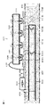
- FIG. 1 is a schematic cross-sectional view of a lighting device according to one embodiment.
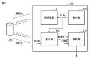
- FIG. 2 is a block diagram showing an example of a schematic configuration of a distance measuring device provided with an illumination device.
- FIG. 3 is a diagram showing an irradiation pattern during spot irradiation of the lighting device.
- FIG. 4 is a diagram showing an irradiation pattern during uniform irradiation of the lighting device.
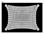
- FIG. 5 is a diagram showing an irradiation pattern when spot irradiation and uniform irradiation are performed simultaneously.
- FIG. 6 is a schematic cross-sectional view showing an example of a light-emitting element according to one embodiment.
- FIG. 1 is a schematic cross-sectional view of a lighting device according to one embodiment.
- FIG. 2 is a block diagram showing an example of a schematic configuration of a distance measuring device provided with an illumination device.
- FIG. 3 is a diagram showing an irradiation pattern during spot irradiation
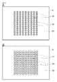
- FIG. 7 is a diagram illustrating an example of a configuration of a light emitting unit according to one embodiment;
- FIG. 8 is an enlarged view of the configuration of the light emitting section in one embodiment.
- 9A is a schematic plan view showing an example of the configuration of the microlens array in FIG. 1
- FIG. 10B is the position of the light emitting unit for spot irradiation with respect to the microlens array shown in FIG. 9A.
- FIG. 10B is the position of the light emitting unit for spot irradiation with respect to the microlens array shown in FIG. 9A. It is a schematic diagram showing.
- FIG. 9A is a schematic plan view showing an example of the configuration of the microlen
- FIG. 11 is a diagram explaining the beam shaping function in one embodiment.
- FIG. 12 is a diagram showing irradiation patterns for an object in one embodiment.
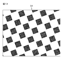
- FIG. 13 is a schematic diagram showing an example of a diffraction element.
- FIG. 14 is a schematic diagram showing the pattern of the light beam that has passed through the diffraction element.
- 15A and 15B are schematic cross-sectional views of diffraction elements according to one embodiment.
- 16A and 16B are schematic diagrams showing liquid crystal elements that can be used instead of diffraction elements.
- 17A and 17B are schematic diagrams showing metamaterials that can be applied instead of diffraction elements.
- FIG. 18 is a diagram illustrating an example of a configuration of a driving circuit of a lighting device;
- FIG. 18 is a diagram illustrating an example of a configuration of a driving circuit of a lighting device
- FIG. 19 is a diagram showing another example of the configuration of the driving circuit of the lighting device.
- FIG. 20 is a diagram explaining a light emission sequence of the lighting device.
- FIG. 21 is a diagram showing a first example of grouping of light emitting elements in the modified example.
- FIG. 22 is a diagram showing a second example of grouping of light emitting elements in the modified example.
- FIG. 23 is a diagram showing a third example of grouping of light emitting elements in the modified example.
- FIG. 24 is a diagram showing a fourth example of grouping of light emitting elements in the modified example.
- FIG. 25 is a diagram showing an example of a top view of a semiconductor laser driving device in an application example.
- FIG. 26 is a diagram showing an example of a cross-sectional view of a semiconductor laser driving device in an application example.
- FIG. 27 is a diagram showing another example of a cross-sectional view of the semiconductor laser driving device in the application example.
- FIG. 1 is a cross-sectional view schematically showing an example of a schematic configuration of a lighting device (lighting device 1) according to an embodiment of the present technology.
- FIG. 2 is a block diagram showing a schematic configuration of a distance measuring device (distance measuring device 100) including the illumination device 1 shown in FIG.
- the distance measuring apparatus 100 includes an illumination device 1, a control unit 220 that controls the illumination device 1, a light receiving unit 210 that receives reflected light reflected from an object for distance measurement, and image data obtained by the light receiving unit 210. and a distance measuring unit 230 that calculates the distance.
- the distance measuring device 100 employs, for example, the ToF (Time of Flight) method or the Structured Light method.
- the ToF method is a method of calculating a distance from the time it takes for a light beam emitted from a distance measuring device to be reflected by an object to be measured and return to the distance measuring device.
- the structured light method is a method in which a distance measuring device irradiates a light beam pattern onto an object to be measured, and the distance is calculated from the distortion of the pattern of the light beam that is reflected and returned to the ranging device.
- the illumination device 1 emits light from a plurality of light emitting units (light emitting units 110 (first light emitting unit) and 120 (second light emitting unit), see FIG. 7).
- the diffraction element 14, which will be described later, is an optical element that tiles the light L1 and expands the irradiation range to the light L2.
- Lights L110 and L120 are for example spot irradiation as shown in FIG. 3, uniform irradiation as shown in FIG. 4, and simultaneous irradiation as shown in FIG.
- the illumination device 1 includes, for example, a light emitting element 11, a microlens array 12 (an example of a second optical member), a collimator lens 13 (an example of a first optical member), a diffraction element 14, and a diffraction element 34. , and a quarter-wave plate 35 .
- the microlens array 12, the collimator lens 13, the diffraction element 14, the diffraction element 34, and the quarter-wave plate 35 are arranged, for example, in this order on the optical path of the light (lights L1 and L2) emitted from the light emitting element 11. ing.
- the light emitting element 11 and the microlens array 12 are held by, for example, a holding section 21, and the collimator lens 13 and the diffraction element 14 are held by, for example, a holding section 22.
- the holding portion 21 has, for example, one anode electrode portion 23 and two cathode electrode portions 24 and 25 on the surface 21S2 opposite to the surface 21S1 that holds the light emitting element 11 and the microlens array 12, for example.
- Each member constituting the lighting device 1 will be described in detail below.
- the light emitting element 11 is, for example, a surface emitting surface emitting semiconductor laser.
- FIG. 6 schematically shows an example of the cross-sectional configuration of the light emitting portions (light emitting portions 110 and 120) of the light emitting element 11. As shown in FIG. Although two light emitting units (light emitting units 110 and 120) are shown in FIG. 6, the number of light emitting units may be at least two. Further, the description of the light emitting section 110 can also be applied to the light emitting section 120 unless otherwise specified.
- Light-emitting element 11 generally includes n-type substrate 130 having main surface 130A and main surface 130B opposite to main surface 130A; an electrode 152, a p-type DBR layer 145 provided on the main surface 130B side of the n-type substrate 130 and having a main surface 145A, and at least two light emitting devices provided on the opposite side of the p-type DBR layer 145 from the main surface 145A. section (for example, light emitting sections 110 and 120).
- a tunnel junction layer 160 is provided between the principal surface 130B of the n-type substrate and the principal surface 145A of the p-type DBR layer 145 . It should be noted that "between” may be provided in between, and does not necessarily need to be in contact with each other. Also, the side may exist in that direction, and does not necessarily need to be in contact.
- the light emitting section 110 is provided on the n-type DBR layer 141 stacked on the p-type DBR layer 145 and having the principal surface 141A and the principal surface 141B opposite to the principal surface 141A, and the principal surface 141B side of the n-type DBR layer 141. and an upper electrode 151 (an example of a second electrode).
- the light emitting element 11 has a cathode electrode lead-out portion divided into at least two regions.
- the upper electrode 151 of the light emitting section 110 is connected to the electrode pad 240 and the upper electrode 151 of the light emitting section 120 is connected to the electrode pad 250 .
- an n-type buffer layer 161 is provided between main surface 130A of n-type substrate 130 and tunnel junction layer 160 .
- the light emitting section 110 includes a p-type spacer layer 144, an active layer 143, an n-type spacer layer 142, an n-type buffer layer 149, a current confinement layer 148, n It has a configuration in which a type DBR layer 141 and an n-type contact layer 146 are stacked in order, and these configurations (hereinafter also referred to as semiconductor layers as appropriate) form a columnar mesa portion 147 .
- An upper electrode 151 is attached to the n-type contact layer 146 . Details of each configuration of the light emitting element 11 will be described below.
- the n-type substrate 130 is, for example, an n-type GaAs substrate.
- n-type impurities include silicon (Si) and selenium (Se).
- the semiconductor layers are each composed of, for example, an AlGaAs-based compound semiconductor.
- An AlGaAs-based compound semiconductor is a compound semiconductor containing at least aluminum (Al) and gallium (Ga) among group 13 elements in the periodic table of elements and at least arsenic (As) among group 15 elements in the periodic table of elements. That's what I mean.
- the n-type DBR layer 141 is formed by alternately stacking low refractive index layers and high refractive index layers (both not shown).
- the low refractive index layer is made of n-type Al x1 Ga 1-x1 As (0 ⁇ x1 ⁇ 1) with a thickness of ⁇ 0 /4n 1 (where ⁇ 0 is the emission wavelength and n 1 is the refractive index), for example.
- the high refractive index layer is composed of, for example, n-type Al x2 Ga 1-x2 As (0 ⁇ x2 ⁇ x1) with a thickness of ⁇ 0 /4n 2 (n2 is the refractive index).
- the n-type spacer layer 142 is composed of, for example, n-type Al x3 Ga 1-x3 As (0 ⁇ x3 ⁇ 1).
- the p-type spacer layer 144 is composed of, for example, p-type Alx5Ga1 -x5As (0 ⁇ x5 ⁇ 1).
- Examples of p-type impurities include zinc (Zn), magnesium (Mg) and beryllium (Be).
- the active layer 143 has a multi-quantum well (MQW) structure.
- the active layer 143 has, for example, a structure in which n-type Al x6 Ga 1-x6 As (0 ⁇ x6 ⁇ 1) thin films and tunnel junction layers are alternately laminated.
- the p-type DBR layer 145 is formed by alternately stacking low refractive index layers and high refractive index layers (both not shown).
- the low refractive index layer is composed of, for example, p-type Al x8 Ga 1-x8 As (0 ⁇ x8 ⁇ 1) with a thickness of ⁇ 0 /4n 3 (n 3 is the refractive index).
- the high refractive index layer is composed of, for example, p-type Al x9 Ga 1-x9 As (0 ⁇ x9 ⁇ x8) with a thickness of ⁇ 0 /4n 4 (n 4 is the refractive index).
- the contact layer 16 is made of, for example, p-type Al x10 Ga 1-x10 As (0 ⁇ x10 ⁇ 1).
- the current confinement layer 148 and the n-type buffer layer 149 are provided within the n-type DBR layer 141, for example.
- the current confinement layer 148 is formed at a position distant from the active layer 143 in relation to the n-type buffer layer 149 .
- the current confinement layer 148 is provided, for example, in the n-type DBR layer 141, instead of the low refractive index layer, at a portion of the low refractive index layer that is several layers away from the active layer 143 side.
- the current confinement layer 148 has a current injection region 148A and a current confinement region 148B.
- the current injection region 148A is formed in the in-plane central region.
- the current confinement region 148B is formed in the peripheral edge of the current injection region 148A, that is, in the outer edge region of the current confinement layer 148, and has an annular shape.
- the current injection region 148A is made of, for example, n-type Al x11 Ga 1-x11 As (0.98 ⁇ x11 ⁇ 1).
- the current confinement region 148B includes, for example, aluminum oxide (Al 2 O 3 ). It is obtained by oxidizing from the side.
- the current constriction layer 148 has a function of constricting current.
- the n-type buffer layer 149 is formed closer to the active layer 143 in relation to the current confinement layer 148 .
- the n-type buffer layer 149 is formed adjacent to the current confinement layer 148 .
- the n-type buffer layer 149 is formed in contact with the surface (lower surface) of the current confinement layer 148 on the active layer 143 side.
- a thin layer having a thickness of, for example, several nanometers may be provided between the current confinement layer 148 and the n-type buffer layer 149 .
- the n-type buffer layer 149 is provided, for example, in the n-type DBR layer 141 at a portion of the high refractive index layer that is several layers away from the current blocking layer 148 instead of the high refractive index layer.
- the n-type buffer layer 149 has an unoxidized region and an oxidized region (both not shown).
- the unoxidized region is mainly formed in the in-plane central region, for example, in a portion in contact with the current injection region 148A.
- the oxidized region is formed around the periphery of the unoxidized region and has an annular shape.
- the oxidized region is mainly formed in the in-plane outer edge region, for example, in a portion in contact with the current confinement region 148B.
- the oxidized region is biased toward the current confinement layer 148 in the portion other than the portion corresponding to the outer edge of the n-type buffer layer 149 .
- the unoxidized region is made of a semiconductor material containing Al, such as n-type Al x12 Ga 1-x12 As (0.85 ⁇ x12 ⁇ 0.98) or n-type In a Al x13 Ga 1-x13- a As (0.85 ⁇ x13 ⁇ 0.98).
- the oxidized region includes, for example, aluminum oxide (Al 2 O 3 ), and includes, for example, n-type Al x12 Ga 1-x12 As or n-type In b Al x13 Ga 1-x13-b As. It is obtained by oxidizing an oxidized layer (not shown) from the side surface side of the mesa portion 147 and the layer side to be oxidized.
- the layer to be oxidized of the n-type buffer layer 149 is made of a material having a higher oxidation rate than the p-type DBR layer 145 and the n-type DBR layer 141 and a lower oxidation rate than the layer to be oxidized of the current confinement layer 148. and thickness.
- the tunnel junction layer 160 is made of a material that allows a tunnel current to flow through this section when an electric current is applied. It consists of a thin film of Tunnel junction layer 160 may be any material that allows tunneling current to flow, as exemplified.
- An n-type buffer layer 161 is provided between the tunnel junction layer 160 and the n-type substrate 130 . As the n-type buffer layer, the same material as the n-type buffer layer 149 can be applied.
- an annular upper electrode 151 having an opening (light exit port 151A) at least in a region facing the current injection region 148A is formed on the upper surface of the mesa portion 147 (upper surface of the n-type contact layer 146).
- An insulating layer (not shown) is formed on the side surface of the mesa portion 147 and the surface of the periphery.
- the upper electrode 151 is connected to the electrode pad 240 or the electrode pad 250 by wiring (not shown) for each of the light emitting portion groups X1 to X9 and the light emitting portion groups Y1 to Y9 (see FIG. 7).
- the electrode pads 240 or 250 are electrically connected by wire bonding.
- a lower electrode 152 is provided on the other surface of the n-type substrate 130 .
- the lower electrode 152 is electrically connected to the anode electrode section 23, for example.
- the anode electrode portion is used as a common electrode and the cathode electrode portions are provided separately.
- the upper electrode 151 is configured by laminating titanium (Ti), platinum (Pt) and gold (Au) in this order, for example, and is electrically connected to the n-type contact layer 146 above the mesa portion 147. It is connected to the.
- the lower electrode 152 has a structure in which, for example, an alloy of gold (Au) and germanium (Ge), nickel (Ni) and gold (Au) are layered in this order from the n-type substrate 130 side. 130 is electrically connected.
- the plurality of light emitting units are, for example, a plurality of light emitting units used for spot irradiation (a plurality of light emitting units 110 for spot irradiation) and a plurality of light emitting units used for uniform irradiation (a plurality of light emitting units for uniform irradiation 120) are arranged in an array on an n-type substrate 130, for example.
- the multiple light emitting units 110 and the multiple light emitting units 120 are electrically isolated from each other.
- the polarization direction of the laser beams L110 emitted from the plurality of light emitting units 110 and the polarization direction of the laser beams L120 emitted from the plurality of light emitting units 120 are different.
- the distance measuring device 100 has a plurality of light-emitting portions, for example, a plurality of light-emitting portions 110 and a plurality of light-emitting portions 120.
- the multiple light emitting units 110 and the multiple light emitting units 120 are electrically connected to each other.
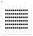
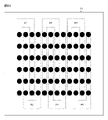
- the plurality of light emitting units 110 includes n (for example, 12 in FIG. 7) light emitting units 110 extending in one direction (for example, the Y-axis direction).
- a plurality of (for example, nine in FIG. 7) light-emitting portion groups X are configured.
- the plurality of light emitting units 120 is a plurality (for example, 9 in FIG. 7) consisting of m (for example, 12 in FIG. 7) light emitting units 120 extending in one direction (for example, the Y-axis direction).
- light emitting portion group Y (light emitting portion groups Y1 to Y9).
- the light emitting unit groups X1 to X9 and the light emitting unit groups Y1 to Y9 are alternately arranged on a rectangular n-type substrate 130, for example, as shown in FIG.
- the groups of light emitting units Y1 to Y9 are provided along the other side facing the one side of the n-type substrate 130, for example. are electrically connected to the electrode pads 250 provided.
- FIG. 7 shows an example in which the groups of light emitting units X1 to X9 and Y1 to Y9 are alternately arranged, the present invention is not limited to this.
- the number of the plurality of light emitting units 110 and the number of the plurality of light emitting units 120 can be arbitrarily arranged according to the desired number, position and amount of light output of light emitting points, respectively.
- the arrangement of the plurality of light emitting units 120 may be arranged every two rows of the arrangement of the plurality of light emitting units 110 .
- FIG. 8 is an enlarged view of part of the arrangement of the plurality of light emitting units 110 and the plurality of light emitting units 120 shown in FIG. It is preferable that the plurality of light emitting portions 110 and the plurality of light emitting portions 120 have different light emitting areas (OA diameters W3, W4). Specifically, the light emitting areas (OA diameter W3) of the multiple light emitting units 110 for spot irradiation are preferably smaller than the light emitting areas (OA diameter W4) of the multiple light emitting units 120 for uniform irradiation.
- the light beams for spot irradiation emitted from the plurality of light emitting units 110 (laser beams L110 (first light) emitted in mutually independent spots on the object to be irradiated 1000, see FIG. 12) are , becomes more focused, allowing a smaller spot to illuminate the object.
- a light beam for uniform irradiation emitted from a plurality of light emitting units 120 (light beams emitted from adjacent light emitting units 120 are superimposed on each other so that light beams emitted from the light emitting units 120 are substantially uniformly distributed over a predetermined range on the irradiation object 1000 .)
- the laser beam L120 (second light, see FIG.
- the opening width W1 of the wiring connecting each of the plurality of light emitting portions 110 becomes smaller than the opening width W2 of the wiring connecting each of the plurality of light emitting portions 120 .
- the number of light emitting units for spot irradiation and the number of light emitting units for uniform irradiation are the same, they may be different.
- the FFP Flu Field Pattern
- the microlens array 12 has, for example, a beam shape of at least one of the light (laser beam L110, laser beam L120) emitted from the plurality of light emitting units 110 for spot irradiation and the plurality of light emitting units 120 for uniform irradiation. is molded and emitted.
- FIG. 9A schematically shows an example of the planar configuration of the microlens array 12, and
- FIG. 9B schematically shows the cross-sectional configuration of the microlens array 12 taken along line II shown in FIG. 9A. It is.
- the microlens array 12 is formed by arranging a plurality of microlenses in an array, and has a plurality of lens portions 12A and parallel plate portions 12B.
- the microlens array 12 is a parallel flat plate as shown in FIG. 10B so that the lens portion 12A faces the plurality of light emitting portions 120 for uniform illumination, as shown in FIG. 10A.
- the portion 12B is arranged to face the plurality of light emitting portions 110 for spot irradiation.
- the laser beams L120 emitted from the plurality of light emitting units 120 are refracted by the lens surface of the lens unit 12A to form a virtual light emitting point P2' within the microlens array 12, for example. .
- the light-emitting points P2 of the plurality of light-emitting sections 120 that are at the same height as the light-emitting points P1 of the plurality of light-emitting sections 110 are aligned with the light emitted from the plurality of light-emitting sections 110 and the light emitted from the plurality of light-emitting sections 120 (laser beams L110, The laser beam L120) is shifted in the optical axis direction (for example, the Z-axis direction).
- the laser beams L110 emitted from the plurality of light emitting units 110 pass through the microlens array 12 as they are. to form a spot-like irradiation pattern as shown in FIG.
- the laser beams L120 emitted from the plurality of light emitting units 120 are refracted by the microlens array 12.
- the laser beams emitted from the light emitting units 120 that are partially adjacent to each other as shown in FIGS.
- an irradiation pattern is formed in which a predetermined range is irradiated with substantially uniform light intensity.
- switching between the light emission of the plurality of light emitting units 110 and the light emission of the plurality of light emitting units 120 enables switching between spot irradiation and uniform irradiation.
- FIG. 11 shows an example in which the microlens array 12 functions as a relay lens, it is not limited to this.
- the virtual light emitting points P ⁇ b>2 ′ of the plurality of light emitting units 120 may be formed between the light emitting units 120 and the microlens array 12 .
- the collimator lens 13 emits the laser beams L110 emitted from the plurality of light emitting sections 110 and the laser beams L120 emitted from the plurality of light emitting sections 120 as substantially parallel light.
- the collimator lens 13 is, for example, a lens for collimating the laser beam L110 and the laser beam L120 emitted from the microlens array 12 and combining them with the diffraction element 14 .
- the diffraction element 14 divides and emits the laser beams L110 emitted from the plurality of light emitting portions 110 and the laser beams L120 emitted from the plurality of light emitting portions 120 respectively.
- a diffraction optical element DOE
- DOE diffraction optical element
- the luminous fluxes of the laser beams L110 and L120 can be tiled, for example, increasing the number of spots during spot irradiation or expanding the irradiation range during uniform irradiation. becomes possible.
- the holding portion 21 and the holding portion 22 are for holding the light emitting element 11, the microlens array 12, the collimator lens 13 and the diffraction element 14.
- the holding part 22 holds the collimator lens 13 and the diffraction element 14 .
- the microlens array 12, the collimator lens 13, and the diffraction element 14 are held by the holding portion 21 and the holding portion 22, respectively, with an adhesive, for example.
- the holding portion 21 and the holding portion 22 hold the light L1 (specifically, the laser beam L110) and the light L2 (specifically, the laser beam L120) emitted from the light emitting element 11 at predetermined positions of the microlens array 12. and are connected to each other so that the lights L1 and L2 that have passed through the collimator lens 13 become substantially parallel lights.
- a plurality of electrode portions are provided on the back surface (surface 21S2) of the holding portion 21.
- the surface 21S2 of the holding portion 21 includes an anode electrode portion 23 common to the plurality of light emitting portions 110 for spot irradiation and the plurality of light emitting portions 120 for uniform irradiation, and a plurality of light emitting portions for spot irradiation.
- a cathode electrode portion 24 of the portion 110 and a cathode electrode portion 25 of a plurality of light emitting portions 120 for uniform irradiation are provided.
- the configuration of the plurality of electrode portions provided on the surface 21S2 of the holding portion 21 is not limited to the above.
- the anode electrode portions may be formed separately, or the anode electrode portions of the plurality of light emitting portions 110 for spot irradiation and the plurality of light emitting portions 120 for uniform irradiation may be formed as a common electrode portion.
- FIG. 1 shows an example in which the microlens array 12 is held by the holding portion 21, it is not limited to this, and may be held by the holding portion 22, for example.
- the collimator lens 13 and the diffraction element 14 may be held by the holding portion 21 .
- FIG. 13 shows the shape of the diffraction element 34 in one embodiment.
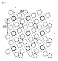
- diffractive element 34 diffracts (or refracts) the light beams emitted by the uniform illumination emitter to increase the number of light beams. For example, one light beam can be split into five as indicated by thin dotted line circles and solid line circles in FIG.
- the light beam emitted from the light emitting portion for spot irradiation is not diffracted by the diffraction element 34, and the light beam is not split. , is irradiated.
- the light beam for uniform irradiation is superimposed with the adjacent light beams, the range in which the adjacent light beams overlap each other (overlapping range) increases, and the light is irradiated as more uniform light. be.
- the light beams for spot irradiation are irradiated with high light intensity without lowering the light intensity one by one.
- the diffraction element 34 in FIGS. 15A and 15B shows cross-sectional views of the diffraction element 34 in one embodiment.
- the diffraction element 34 in FIGS. 15A and 15B has, for example, a three-layer structure in which a first layer 171, a second layer 172, and a third layer 173 are joined in this order.
- the refractive index of the tri-layer 173 is n3.
- the refractive index of the second layer 172 varies with direction, with the refractive index in the Y direction shown in FIG. 15A being n2y and the refractive index in the X direction shown in FIG. 8B being n2x.
- Each layer can be made of any material as long as it satisfies these refractive index relationships.
- the diffraction element 34 since the diffraction element 34 has different refractive indices in the X direction and the Y direction, it acts as a parallel plate for polarized light in a certain direction (X direction), and acts as a parallel plate for polarized light in a direction (Y direction) acts as a diffraction element that diffracts (refracts) the light beam.
- the diffraction element 34 is a polarization diffraction element that refracts or diffracts a light beam traveling in a predetermined direction (specific direction) to change the polarization characteristics of the light beam emitted from the uniformly illuminated light emitting portion. can be done.
- a volume hologram may be used instead of the diffraction element 34 .
- the diffraction element 34 may be one that refracts light, and may be, for example, a Fresnel lens.
- the diffraction element 34 diffracts or refracts the laser beam L120 emitted from the light emitting unit for uniform irradiation, but does not exert any effect on the laser beam L110 emitted from the light emitting unit for spot irradiation, and transmits the laser beam L110 as it is. . That is, diffraction element 34 acts differently on laser beam L110 and laser beam L120. As a result, distance measurement can be performed without reducing the intensity of the light beam emitted from the light emitting unit for spot irradiation.
- the positions of the diffraction element 14 and the diffraction element 34 described above may be reversed, and the optical diffraction surface may be arranged so as to overlap both sides of one optical element or one side of one optical surface. .
- the function of the diffraction grating 14 exhibits the same effect regardless of the polarization direction of light.
- a quarter-wave plate 35 is arranged above the diffraction element 34 .
- the quarter-wave plate 35 converts the light beam irradiated to the object for distance measurement into circularly polarized light, thereby suppressing changes in reflection characteristics due to the material and orientation of the object for distance measurement.
- both the diffraction element 34 and the quarter-wave plate 35 may be formed in one optical element.
- an organic liquid crystal element 175 having different orientations in the X and Y directions which is schematically shown in FIGS. 16A and 16B, can be used.
- a circuit configuration, a flexible cable, or the like for switching the orientation of the organic liquid crystal element 175 is not required, and the problem of time for switching the orientation of the organic liquid crystal element 175 does not occur.
- An inorganic liquid crystal element may be used instead of the organic liquid crystal element 175 .
- Inorganic liquid crystal elements have better temperature characteristics and heat resistance than organic liquid crystal elements, and can be used for applications that require high reliability, such as in-vehicle applications.
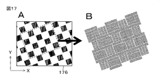
- a so-called metamaterial 176 can be used, which has microstructures on a sub-wavelength scale of the light beam, schematically shown in FIGS. 17A and 17B.
- FIG. 17B is an enlarged view of a portion of the metamaterial 176 shown in FIG. 17A.
- the metamaterial 176 can generate different diffraction characteristics depending on the polarization direction.
- the metamaterial 176 can have the function of the quarter-wave plate 35 (for example, the function of converting circularly polarized light into linearly polarized light). .
- the configuration related to the quarter wave plate 35 can be eliminated, and the size and cost of the device can be reduced.
- the function of the collimator lens 13 may also be formed of a metamaterial, and the collimator lens 13, the diffraction element 34 and the quarter wave plate 35 may be formed together in one optical element.
- FIG. 18 shows an example of the configuration of the driving circuit of the lighting device 1.
- the anodes of the first light emitting unit group 181 and the second light emitting unit group 182 are connected to a power supply (VCC).
- the cathodes of the first light emitting unit group 181 are connected to the drive unit 265
- the cathodes of the second light emitting unit group 182 are connected to the drive unit 266 .
- the first light-emitting portion group 181 is, for example, a set of light-emitting portions 110 connected to the electrode pads 240 .
- the second light-emitting portion group 182 is, for example, a set of light-emitting portions 120 connected to the electrode pads 250 .
- the switching of the light emitting unit group can be realized by outputting modulation signals from two driving units and using an external changeover switch.
- an n-type MOSFET Metal Oxide Semiconductor Field Effect Transistor
- each of the drive sections 265 and 266 is supplied with a modulation signal that defines the timing of ON/OFF modulation
- each of the drive sections 265 and 266 connects the ground and the first light emitting section group 181 or the second light emitting section group 182 at the ON timing.
- a current flows through the first group of light emitting units 181 and the second group of light emitting units 182 at the ON timing, causing light emission.
- the cathodes of the first light-emitting portion group 181 and the second light-emitting portion group 182 are completely separated, and the driving portion 265 and the driving portion 266 are provided respectively. Each can be driven with different waveforms (timing and current).
- each of the driving section 265 and the driving section 266 may be a P-type MOSFET or a bipolar transistor.
- the driving section 265 and the driving section 266 may be provided outside the lighting device 1, for example, or may be built in the holding section 21, for example. Alternatively, the light emitting element 11 and each drive section may be directly connected.
- FIG. 18 uses a common anode electrode
- a circuit configuration in which a common cathode electrode is used as shown in FIG. 19 is also possible. In the circuit configuration shown in FIG. 19, switching between the first light-emitting unit group 181 and the second light-emitting unit group 182 is accomplished by, for example, using one driving unit 270 and turning on/off the external switches SW1 and SW2 in a complementary manner. It is done by
- FIG. 20 shows an example of the light emission sequence of the lighting device 1.
- FIG. A section for generating one distance measurement image is called a “frame”, and one frame is set to a time such as 33.3 msec (frequency of 30 Hz).
- a plurality of accumulation intervals with different conditions can be provided in a frame. Although eight accumulation intervals are shown in FIG. 20, the number is not limited to this.
- the first light emitting unit group 181 emits light in one frame, and the light receiving unit 210 (see FIG. 2) receives the reflected light to generate a ranging image.
- the second light emitting unit group 182 is caused to emit light, and the light receiving unit 210 receives the reflected light to generate a ranging image.
- the first light emitting unit group 181 and the second light emitting unit group 182 are switched every frame in FIG. 20, they may be switched every multiple frames.
- the switching of the light emission of the first light emitting unit group 181 and the second light emitting unit group 182 may be performed, for example, in units of one frame, may be performed in units of blocks, or may be performed in units of a plurality of blocks. . This makes it possible to switch between spot irradiation and uniform irradiation at a faster speed than, for example, a method of mechanically switching the focal positions of laser beams emitted from a plurality of light emitting units.
- the third optical member diffracts or refracts the light beam emitted from the light emitting unit for uniform irradiation, thereby increasing the overlapping range of the uniform irradiation pattern.
- the accuracy of ranging can be improved.
- the intensity of the light beam emitted from the light emitting section for spot irradiation can be reduced by making the third optical member have no effect on the light beam emitted from the light emitting section for spot irradiation. distance measurement can be performed without
- the microlens array 12 described in one embodiment may be omitted.
- the laser beam L110 emitted from the light emitting unit 110 is light for spot irradiation that passes through the diffraction element 14 or the like as it is, and the laser beam L120 emitted from the light emitting unit 120 is diffracted by the diffraction element 14 or the like.
- the laser beam L120 has an increased number of spots. Since the laser beam L110 has a high light intensity, long distance measurement is possible, and since the laser beam L120 has a large number of spots, there is an advantage that the resolution in distance measurement is relatively high.
- the light emitting elements 11 in one embodiment may be grouped.
- 21 to 23 are diagrams showing examples of grouping of the light emitting elements 11 in the application example of the present technology.
- FIG. 21 it is assumed that one region is formed for each of multiple columns (two columns in this example) and switching is performed for each region.
- FIG. 22 it is assumed that one frame is further vertically divided into two to form rectangular regions, and switching is performed for each region.
- FIG. 23 it is assumed that the number of divisions in the vertical direction is three and switching is performed for each region.
- flexible adjustment can be performed by switching light emission in units of light emitting regions. Light emission may be switched for each frame, or may be a block within a frame. It is also possible to recognize the position of an object whose distance is to be measured and to emit light in that area.
- FIG. 24 is a diagram showing another example of grouping of the light emitting elements 11 in the modified example of the present technology.
- This example shows an example of grouping by two columns so that each column is alternately combined.
- the 1st and 3rd columns are area A1
- the 2nd and 4th columns are area A2
- the 5th and 7th columns are area A3
- the 6th and 8th columns are area A4, and the 9th column is
- the 11th row forms an area A5, and the 10th and 12th rows form an area A6. This makes it possible to control the switching of light emission every two columns. As a result, it is possible to reduce power consumption by area switching and achieve high light output within the laser safety standards while taking countermeasures against multipath.
- FIG. 25 is a diagram showing an example of a top view of a semiconductor laser driving device 300 in an application example.
- the semiconductor laser drive device 300 is intended for distance measurement by ToF.
- ToF has the feature that depth accuracy is high although it is not as high as structured light, and that it can operate without problems even in a dark environment.
- a semiconductor laser 301 In the semiconductor laser driving device 300, a semiconductor laser 301, a photodiode 420, and a passive component 430 are electrically connected and mounted by wire bonding on the surface of a substrate 400 containing a laser driver 500 (an example of a driving element).
- Substrate 400 is assumed to be a printed wiring board.
- the illumination device 1 or 1B described above can be applied to the semiconductor laser 301, and the light receiving section 210 in FIG. 1, for example, can be applied to the photodiode.
- the semiconductor laser 301 is a semiconductor device that emits laser light by passing a current through a PN junction of a compound semiconductor.
- compound semiconductors to be used here include aluminum gallium arsenide (AlGaAs), indium gallium arsenide phosphide (InGaAsP), aluminum gallium indium phosphide (AlGaInP), and gallium nitride (GaN).
- a laser driver 500 is a driver integrated circuit (IC: Integrated Circuit) for driving the semiconductor laser 301 .
- the laser driver 500 is built in the substrate 400 in a face-up state.
- As for the electrical connection with the semiconductor laser 301 it is desirable to make the wiring length as short as possible because it is necessary to reduce the wiring inductance.
- the photodiode 420 is a diode for detecting light. This photodiode 420 is used for APC control (Automatic Power Control) for monitoring the light intensity of the semiconductor laser 301 and maintaining the output of the semiconductor laser 301 constant.
- APC control Automatic Power Control
- Passive components 430 are circuit components other than active elements such as capacitors and resistors. Passive components 430 include decoupling capacitors for driving semiconductor laser 301 .
- FIG. 26 is a diagram showing an example of a cross-sectional view of the semiconductor laser driving device 300 in the application example of the present technology.
- the substrate 400 incorporates the laser driver 500, and the semiconductor laser 301 and the like are mounted on its surface. Connections between the semiconductor lasers 301 and the laser drivers 500 in the substrate 400 are made through connection vias 401 . By using the connection via 401, it is possible to shorten the wiring length.
- the semiconductor laser 301 is assumed to be a vertical cavity surface emitting laser (VCSEL).
- the VCSEL has a substrate 310 as substrate material and a common anode underneath.
- the light-emitting points are formed as trapezoidal-shaped mesas, each containing a light-emitting element 341 .
- the anode electrode of the light emitting element 341 is connected to the signal line pattern 406 on the substrate 400 via the connection layer.
- the cathode electrodes of the light emitting elements are connected to the metal layers 330A, 330B, and one ends of the driver elements 501A, 501B are connected to the metal layers 330A, 330B via wire bondings 410A, 410B.
- the connection layer can be formed by either silver paste or solder.
- the wire bondings 410A, 410B and the driver elements 510A, 510B are connected by connection vias 411A, 411B.
- the light emitting point of the semiconductor laser 301 is located just above the substrate 400, the heat generated at the light emitting point can be efficiently released to the component-embedded substrate.
- the substrate 400 includes thermal vias for heat dissipation.
- Each component mounted on the substrate 400 is a heat source, and heat generated in each component can be dissipated from the back surface of the substrate 400 by using thermal vias.
- a capacitor 409 is mounted as a decoupling capacitor on the substrate 400 and connected between the pattern 406 and the ground (GND) 408. Since the capacitor 409 is provided as a decoupling capacitor, the charge stored in this capacitor 409 can be used as the drive current for the semiconductor laser 301 . As described above, according to the application example, when the laser is modulated at high speed, the charge stored in the capacitor 409 mounted in the immediate vicinity of the semiconductor laser 301 becomes the driving current of the semiconductor laser 301. Modulation can be achieved.
- the light emitting element 341 may be installed upside down. In this case, emitted light 309 from the light emitting element 341 is emitted through the substrate 310 .
- the cathode of the light emitting element 341 is connected to the signal line pattern 406 on the substrate 400 via bumps 349A and 349B, and the driver elements 501A and 501B of the laser driver 500 incorporated in the substrate 400 via connection vias 411A and 411B. is connected to one end of the The other ends of driver elements 501A and 501B are connected to ground (GND) 408 .
- a metal layer 330 is provided on the surface of the substrate 310 on the light emitting point side, and is connected to the power source pattern 407 of the substrate 400 via wire bonding 410 .
- the metal layer 330 may be a transparent electrode such as ITO (Indium Tin Oxide).
- the side of the light emitting element 341 that is not the light emitting point side is connected to the driver elements 501A and 501B via bumps 349A and 349B, patterns 406A and 406B and connection vias 411A and 411B.
- the bumps 349A and 349B can be made of either gold (Au), copper (Cu), or solder.
- the present technology can also have the following configuration.
- a light emitting element having a plurality of first light emitting units and a plurality of second light emitting units; a first optical member that emits the plurality of first light beams emitted from the plurality of first light emitting portions and the plurality of second light beams emitted from the plurality of second light emitting portions in substantially parallel relation to each other;
- a second optical member that emits light; a third optical member;
- the third optical member is arranged on an optical path of the plurality of first lights and the plurality of second lights, and the action of the third optical member on the plurality of first lights and the plurality of different from the effect on the second light of the lighting device.
- the illumination device does not act on the plurality of first lights and refracts or diffracts the plurality of second lights in a predetermined direction.
- the plurality of first lights emitted from the plurality of first light-emitting units are lights irradiated to an irradiation target in mutually independent spots, A part of the plurality of second lights emitted from the plurality of second light emitting units overlaps with the second light emitted from the adjacent second light emitting units. and the illumination device according to (1) or (2), wherein the light is applied to an object to be irradiated substantially uniformly over a predetermined range.
- the third optical member is an optical member that increases an overlapping range in which a part of the plurality of second lights overlap each other.
- the plurality of first lights emitted from the plurality of first light emitting units and the plurality of second lights emitted from the plurality of second light emitting units have different polarization characteristics (1 ) to (4).
- the illumination device according to any one of (1) to (6), wherein the third optical member is a liquid crystal element.
- a lighting device according to any one of (1) to (8); a control unit that controls the lighting device; a light receiving unit that receives reflected light reflected from an object to be irradiated;
- a distance measuring device comprising: a distance measuring unit that calculates a distance from image data obtained by the light receiving unit.
Landscapes
- Physics & Mathematics (AREA)
- General Physics & Mathematics (AREA)
- Engineering & Computer Science (AREA)
- Electromagnetism (AREA)
- Condensed Matter Physics & Semiconductors (AREA)
- Optics & Photonics (AREA)
- Computer Networks & Wireless Communication (AREA)
- Radar, Positioning & Navigation (AREA)
- Remote Sensing (AREA)
- Measurement Of Optical Distance (AREA)
- Semiconductor Lasers (AREA)
Abstract
Description
複数の第1の発光部および複数の第2の発光部を有する発光素子と、
複数の第1の発光部から出射された複数の第1の光および複数の第2の発光部から出射された複数の第2の光をそれぞれ略平行にして出射する第1の光学部材と、
複数の第1の光および複数の第2の光のうちの少なくとも一方のビーム形状を成形し、互いに異なるビーム形状を有する光として、複数の第1の光および複数の第2の光を出射する第2の光学部材と、
第3の光学部材と
を備え、
第3の光学部材は、複数の第1の光および複数の第2の光の光路上に配置され、第3の光学部材による複数の第1の光への作用と複数の第2の光への作用とが異なる
照明装置である。
上述した照明装置と、
照明装置を制御する制御部と、
照射対象物から反射された反射光を受光する受光部と、
受光部で得られた画像データから距離を算出する測距部と
を有する
測距装置である。
<1.一実施の形態>
<2.変形例>
<3.応用例>
図1は、本技術の一実施の形態に係る照明装置(照明装置1)の概略構成の一例を模式的に表した断面図である。図2は、図1に示した照明装置1を備えた測距装置(測距装置100)の概略構成を表したブロック図である。測距装置100は、照明装置1と、照明装置1を制御する制御部220と、測距対象物から反射された反射光を受光する受光部210と、受光部210で得られた画像データから距離を算出する測距部230とを有する。
照明装置1は、例えば、発光素子11と、マイクロレンズアレイ12(第2の光学部材の一例)と、コリメータレンズ13(第1の光学部材の一例)と、回折素子14と、回折素子34と、1/4波長板35とを有する。
発光素子11は、例えば、表面出射型の面発光半導体レーザである。図6は、発光素子11の発光部(発光部110,120)の断面構成の一例を模式的に表したものである。なお、図6では、2つの発光部(発光部110,120)が示されているが、発光部の個数は少なくとも2つであればよい。また、特に断らない限り、発光部110の説明は発光部120に対しても適用することができる。
複数の発光部は、例えば、スポット照射に用いられる複数の発光部(スポット照射用の複数の発光部110)と、一様照射に用いられる複数の発光部(一様照射用の複数の発光部120)とが、例えば、n型基板130上にアレイ状に配置された構成を有する。複数の発光部110および複数の発光部120は、互いに電気的に分離されている。本実施形態では、複数の発光部110から出射されるレーザビームL110の偏光方向と複数の発光部120から出射されるレーザビームL120の偏光方向とが異なっている。
マイクロレンズアレイ12は、例えば、スポット照射用の複数の発光部110および一様照射用の複数の発光部120から出射される光(レーザビームL110,レーザビームL120)のうちの少なくとも一方のビーム形状を成形して出射するものである。図9Aは、マイクロレンズアレイ12の平面構成の一例を模式的に表したものであり、図9Bは、図9Aに示したI-I線におけるマイクロレンズアレイ12の断面構成を模式的に表したものである。マイクロレンズアレイ12は、複数のマイクロレンズがアレイ状に配置されたものであり、複数のレンズ部12Aと、平行平板部12Bとを有している。
保持部21および保持部22は、発光素子11、マイクロレンズアレイ12、コリメータレンズ13および回折素子14を保持するためのものである。具体的には、保持部21は、上面(面21S1)に設けられた凹部C内に発光素子11を保持し、面21S1に沿ってマイクロレンズアレイ12を保持している。保持部22は、コリメータレンズ13および回折素子14を保持している。マイクロレンズアレイ12、コリメータレンズ13および回折素子14は、例えば、接着剤によって、それぞれ、保持部21および保持部22に保持されている。保持部21および保持部22は、発光素子11から出射された光L1(具体的には、レーザビームL110)および光L2(具体的には、レーザビームL120)をマイクロレンズアレイ12の所定の位置に入射させると共に、コリメータレンズ13を透過した光L1,L2が略平行光となるように、互いに接続されている。
図13は、一実施の形態における回折素子34の形状を示す。一実施の形態では、回折素子34は一様照射用の発光部から出射される光ビームを回折(または屈折)し、光ビームの数を増やす。例えば、図14における細点線の丸印と実線の丸印とで示されるように、1つの光ビームを5分割することができる。これに対して、スポット照射用の発光部から出射される光ビームは、回折素子34で回折されずに、光ビームは分割されず、図14における太点線の丸印で示されるように、そのまま、照射される。回折素子34の作用により、一様照射用の光ビームは、隣り合う光ビームと重畳され、隣り合う光ビームどうしがお互いに重畳する範囲(重畳範囲)が増加し、より均一な光として照射される。スポット照射用の光ビームは、一つ一つが光強度を落とすことなく、光強度が高いまま照射される。
第3の光学部材の他の例について説明する。上述した回折素子34の代わりに、図16Aおよび図16Bに模式的に示される、X方向およびY方向の配向が異なる有機液晶素子175を用いることができる。このとき、VCSELの発光切替えによってビーム光の偏光の向きを変えることができるので、ビーム光の偏光の向きを変えるために有機液晶素子175の配向を切替える必要がない。このため、有機液晶素子175の配向の切替え用の回路構成やフレキシブルケーブル等は不要であり、また、有機液晶素子175の配向の切替え時間の問題が発生しない。有機液晶素子175の代わりに、無機液晶素子を用いてもよい。無機液晶素子は有機液晶素子に比べて温度特性や耐熱性が良く、車載用途など高信頼性が要求される用途にも利用できる。
図18は、照明装置1の駆動回路の構成の一例を表したものである。同図に示すように第1発光部群181及び第2発光部群182のアノードは電源(VCC)に接続されている。また、第1発光部群181のカソードは駆動部265に接続され、第2発光部群182のカソードは駆動部266に接続されている。第1発光部群181は、例えば、電極パット240に接続される発光部110の集合である。また、第2発光部群182は、例えば、電極パット250に接続される発光部120の集合である。例えば、発光部群の切替は、2つの駆動部から変調信号を出力し、外付けの切替えスイッチにより実現することができる。
以上、本開示の実施の形態について具体的に説明したが、本開示の内容は上述した実施の形態に限定されるものではなく、本開示の技術的思想に基づく各種の変形が可能である。以下、複数の変形例のそれぞれについて説明する。なお、一実施の形態と同一または同質の構成については同一の参照符号を付し、重複した説明を適宜、省略する。
次に、応用例について説明する。本応用例は、本技術を半導体レーザ駆動装置300として構成したものである。図25は、応用例における半導体レーザ駆動装置300の上面図の一例を示す図である。半導体レーザ駆動装置300は、ToFによる距離の測定を想定したものである。ToFは、ストラクチャードライトほどではないものの奥行き精度が高く、また、暗い環境下でも問題なく動作可能という特徴を有する。他にも、装置構成の単純さや、コストなどにおいて、ストラクチャードライトやステレオカメラなどの他の方式と比べてメリットが多いと考えられる。
(1)
複数の第1の発光部および複数の第2の発光部を有する発光素子と、
前記複数の第1の発光部から出射された複数の第1の光および前記複数の第2の発光部から出射された複数の第2の光をそれぞれ略平行にして出射する第1の光学部材と、
前記複数の第1の光および前記複数の第2の光のうちの少なくとも一方のビーム形状を成形し、互いに異なるビーム形状を有する光として、前記複数の第1の光および前記複数の第2の光を出射する第2の光学部材と、
第3の光学部材と
を備え、
前記第3の光学部材は、前記複数の第1の光および前記複数の第2の光の光路上に配置され、前記第3の光学部材による前記複数の第1の光への作用と前記複数の第2の光への作用とが異なる
照明装置。
(2)
前記第3の光学部材は、前記複数の第1の光には作用をせず、前記複数の第2の光を所定方向に屈折または回折する
(1)に記載の照明装置。
(3)
前記複数の第1の発光部から出射された前記複数の第1の光は、照射対象物に対して互いに独立したスポット状に照射される光であり、
前記複数の第2の発光部から出射された前記複数の第2の光は、前記第2の光の一部が、隣り合う第2の発光部から出射された第2の光と重畳することで、照射対象物に対して、所定の範囲に略一様に照射される光である
(1)又は(2)に記載の照明装置。
(4)
前記第3の光学部材は、前記複数の第2の光の一部が互いに重なる重畳範囲を増加させる光学部材である
(3)に記載の照明装置。
(5)
前記複数の第1の発光部から出射された前記複数の第1の光と、前記複数の第2の発光部から出射された前記複数の第2の光とが、異なる偏光特性を有する
(1)から(4)までの何れかに記載の照明装置。
(6)
前記第3光学部材が偏光回折素子である
(1)から(5)までの何れかに記載の照明装置。
(7)
前記第3光学部材が液晶素子である
(1)から(6)までの何れかに記載の照明装置。
(8)
前記第3光学部材がメタマテリアルである
(1)から(7)までの何れかに記載の照明装置。
(9)
(1)から(8)までの何れかに記載の照明装置と、
前記照明装置を制御する制御部と、
照射対象物から反射された反射光を受光する受光部と、
前記受光部で得られた画像データから距離を算出する測距部と
を有する
測距装置。
Claims (9)
- 複数の第1の発光部および複数の第2の発光部を有する発光素子と、
前記複数の第1の発光部から出射された複数の第1の光および前記複数の第2の発光部から出射された複数の第2の光をそれぞれ略平行にして出射する第1の光学部材と、
前記複数の第1の光および前記複数の第2の光のうちの少なくとも一方のビーム形状を成形し、互いに異なるビーム形状を有する光として、前記複数の第1の光および前記複数の第2の光を出射する第2の光学部材と、
第3の光学部材と
を備え、
前記第3の光学部材は、前記複数の第1の光および前記複数の第2の光の光路上に配置され、前記第3の光学部材による前記複数の第1の光への作用と前記複数の第2の光への作用とが異なる
照明装置。 - 前記第3の光学部材は、前記複数の第1の光には作用をせず、前記複数の第2の光を所定方向に屈折または回折する
請求項1に記載の照明装置。 - 前記複数の第1の発光部から出射された前記複数の第1の光は、照射対象物に対して互いに独立したスポット状に照射される光であり、
前記複数の第2の発光部から出射された前記複数の第2の光は、前記第2の光の一部が、隣り合う第2の発光部から出射された第2の光と重畳することで、照射対象物に対して、所定の範囲に略一様に照射される光である
請求項1に記載の照明装置。 - 前記第3の光学部材は、前記複数の第2の光の一部が互いに重なる重畳範囲を増加させる光学部材である
請求項3に記載の照明装置。 - 前記複数の第1の発光部から出射された前記複数の第1の光と、前記複数の第2の発光部から出射された前記複数の第2の光とが、異なる偏光特性を有する
請求項1に記載の照明装置。 - 前記第3光学部材が偏光回折素子である
請求項1に記載の照明装置。 - 前記第3光学部材が液晶素子である
請求項1に記載の照明装置。 - 前記第3光学部材がメタマテリアルである
請求項1に記載の照明装置。 - 請求項1に記載の照明装置と、
前記照明装置を制御する制御部と、
照射対象物から反射された反射光を受光する受光部と、
前記受光部で得られた画像データから距離を算出する測距部と
を有する
測距装置。
Priority Applications (4)
| Application Number | Priority Date | Filing Date | Title |
|---|---|---|---|
| JP2023510623A JP7756153B2 (ja) | 2021-03-31 | 2022-02-15 | 照明装置および測距装置 |
| CN202280023538.7A CN117044050A (zh) | 2021-03-31 | 2022-02-15 | 照明装置和测距装置 |
| DE112022001894.1T DE112022001894T5 (de) | 2021-03-31 | 2022-02-15 | Beleuchtungsvorrichtung und abstandsmessvorrichtung |
| US18/279,817 US20240310489A1 (en) | 2021-03-31 | 2022-02-15 | Illumination device and distance measuring device |
Applications Claiming Priority (2)
| Application Number | Priority Date | Filing Date | Title |
|---|---|---|---|
| JP2021-062059 | 2021-03-31 | ||
| JP2021062059 | 2021-03-31 |
Publications (1)
| Publication Number | Publication Date |
|---|---|
| WO2022209376A1 true WO2022209376A1 (ja) | 2022-10-06 |
Family
ID=83458802
Family Applications (1)
| Application Number | Title | Priority Date | Filing Date |
|---|---|---|---|
| PCT/JP2022/005970 Ceased WO2022209376A1 (ja) | 2021-03-31 | 2022-02-15 | 照明装置および測距装置 |
Country Status (5)
| Country | Link |
|---|---|
| US (1) | US20240310489A1 (ja) |
| JP (1) | JP7756153B2 (ja) |
| CN (1) | CN117044050A (ja) |
| DE (1) | DE112022001894T5 (ja) |
| WO (1) | WO2022209376A1 (ja) |
Cited By (2)
| Publication number | Priority date | Publication date | Assignee | Title |
|---|---|---|---|---|
| WO2024024354A1 (ja) * | 2022-07-26 | 2024-02-01 | ソニーセミコンダクタソリューションズ株式会社 | 照明装置、測距装置及び車載装置 |
| JP2024060604A (ja) * | 2022-10-19 | 2024-05-02 | ツー-シックス デラウェア インコーポレイテッド | 偏光/レンズ付き背面発光式(bse)垂直共振器型面発光レーザー(vcsel) |
Citations (7)
| Publication number | Priority date | Publication date | Assignee | Title |
|---|---|---|---|---|
| JP2006189728A (ja) * | 2005-01-07 | 2006-07-20 | Ricoh Co Ltd | 光源ユニット、光走査装置及び画像形成装置等 |
| US20140376092A1 (en) * | 2013-06-19 | 2014-12-25 | Primesense Ltd. | Integrated structured-light projector |
| JP2018511785A (ja) * | 2015-02-19 | 2018-04-26 | コーニンクレッカ フィリップス エヌ ヴェKoninklijke Philips N.V. | 赤外線レーザ照明装置 |
| WO2019017044A1 (ja) * | 2017-07-18 | 2019-01-24 | ソニー株式会社 | 発光素子及び発光素子アレイ |
| JP2019113530A (ja) * | 2017-12-22 | 2019-07-11 | 株式会社デンソー | 距離測定装置、認識装置、及び距離測定方法 |
| CN212626514U (zh) * | 2020-08-21 | 2021-02-26 | 宁波舜宇奥来技术有限公司 | 发射端模组和结构光系统 |
| JP2021048206A (ja) * | 2019-09-18 | 2021-03-25 | ソニーセミコンダクタソリューションズ株式会社 | 半導体レーザ駆動装置、電子機器、および、半導体レーザ駆動装置の製造方法 |
Family Cites Families (3)
| Publication number | Priority date | Publication date | Assignee | Title |
|---|---|---|---|---|
| US11320588B1 (en) * | 2012-04-16 | 2022-05-03 | Mohammad A. Mazed | Super system on chip |
| US10244181B2 (en) * | 2009-02-17 | 2019-03-26 | Trilumina Corp. | Compact multi-zone infrared laser illuminator |
| US20220179147A1 (en) * | 2020-12-04 | 2022-06-09 | Facebook Technologies, Llc | Patterned backlight for display panel |
-
2022
- 2022-02-15 JP JP2023510623A patent/JP7756153B2/ja active Active
- 2022-02-15 US US18/279,817 patent/US20240310489A1/en active Pending
- 2022-02-15 CN CN202280023538.7A patent/CN117044050A/zh active Pending
- 2022-02-15 DE DE112022001894.1T patent/DE112022001894T5/de active Pending
- 2022-02-15 WO PCT/JP2022/005970 patent/WO2022209376A1/ja not_active Ceased
Patent Citations (7)
| Publication number | Priority date | Publication date | Assignee | Title |
|---|---|---|---|---|
| JP2006189728A (ja) * | 2005-01-07 | 2006-07-20 | Ricoh Co Ltd | 光源ユニット、光走査装置及び画像形成装置等 |
| US20140376092A1 (en) * | 2013-06-19 | 2014-12-25 | Primesense Ltd. | Integrated structured-light projector |
| JP2018511785A (ja) * | 2015-02-19 | 2018-04-26 | コーニンクレッカ フィリップス エヌ ヴェKoninklijke Philips N.V. | 赤外線レーザ照明装置 |
| WO2019017044A1 (ja) * | 2017-07-18 | 2019-01-24 | ソニー株式会社 | 発光素子及び発光素子アレイ |
| JP2019113530A (ja) * | 2017-12-22 | 2019-07-11 | 株式会社デンソー | 距離測定装置、認識装置、及び距離測定方法 |
| JP2021048206A (ja) * | 2019-09-18 | 2021-03-25 | ソニーセミコンダクタソリューションズ株式会社 | 半導体レーザ駆動装置、電子機器、および、半導体レーザ駆動装置の製造方法 |
| CN212626514U (zh) * | 2020-08-21 | 2021-02-26 | 宁波舜宇奥来技术有限公司 | 发射端模组和结构光系统 |
Cited By (3)
| Publication number | Priority date | Publication date | Assignee | Title |
|---|---|---|---|---|
| WO2024024354A1 (ja) * | 2022-07-26 | 2024-02-01 | ソニーセミコンダクタソリューションズ株式会社 | 照明装置、測距装置及び車載装置 |
| JP2024060604A (ja) * | 2022-10-19 | 2024-05-02 | ツー-シックス デラウェア インコーポレイテッド | 偏光/レンズ付き背面発光式(bse)垂直共振器型面発光レーザー(vcsel) |
| JP7737434B2 (ja) | 2022-10-19 | 2025-09-10 | ツー-シックス デラウェア インコーポレイテッド | 偏光垂直共振器型面発光レーザー(vcsel)システム |
Also Published As
| Publication number | Publication date |
|---|---|
| DE112022001894T5 (de) | 2024-02-08 |
| JPWO2022209376A1 (ja) | 2022-10-06 |
| JP7756153B2 (ja) | 2025-10-17 |
| CN117044050A (zh) | 2023-11-10 |
| US20240310489A1 (en) | 2024-09-19 |
Similar Documents
| Publication | Publication Date | Title |
|---|---|---|
| CN110710072B (zh) | 具有结合光束转向的超小型垂直腔表面发射激光发射器的器件 | |
| US20250023323A1 (en) | Surface emitting laser package | |
| US12566266B2 (en) | Lighting device and distance measurement apparatus | |
| WO2020158744A1 (en) | Surface emitting laser module, optical device, and surface emitting laser substrate | |
| US11837570B2 (en) | Light emitting device package | |
| US12003075B2 (en) | Surface emitting laser device and surface emitting laser apparatus having the same | |
| JP7756153B2 (ja) | 照明装置および測距装置 | |
| US12394956B2 (en) | Surface emitting laser package having a diffusion part having glass and polymer layers and light emitting device including the same | |
| JP6799828B2 (ja) | 光源装置 | |
| JP2023182875A (ja) | 照明装置および測距装置 | |
| JP2022500880A (ja) | 位相結合されたレーザ装置、および位相結合されたレーザ装置を製造するための方法 | |
| US20240170921A1 (en) | Light emitting element, illumination device, and distance measuring device | |
| KR102534590B1 (ko) | 표면발광레이저 패키지 | |
| JP5102652B2 (ja) | 発光装置 | |
| KR102607445B1 (ko) | 표면발광레이저 패키지 | |
| KR102486332B1 (ko) | 표면발광 레이저패키지 및 이를 포함하는 광 모듈 | |
| KR102925196B1 (ko) | 표면발광 레이저소자 및 이를 구비한 거리측정 장치 | |
| JP7758917B2 (ja) | 光源装置 | |
| US20240219526A1 (en) | Illumination device and ranging device | |
| US20240183946A1 (en) | Illumination device and distance measuring device | |
| KR102660071B1 (ko) | 표면광방출레이저 패키지 및 자동초점장치 | |
| JP2026504949A (ja) | パッケージ構造 | |
| WO2023176205A1 (ja) | 発光装置 | |
| JP2025070001A (ja) | 発光装置、光源選択方法、及び、発光装置の製造方法 |
Legal Events
| Date | Code | Title | Description |
|---|---|---|---|
| 121 | Ep: the epo has been informed by wipo that ep was designated in this application |
Ref document number: 22779603 Country of ref document: EP Kind code of ref document: A1 |
|
| WWE | Wipo information: entry into national phase |
Ref document number: 2023510623 Country of ref document: JP |
|
| WWE | Wipo information: entry into national phase |
Ref document number: 18279817 Country of ref document: US |
|
| WWE | Wipo information: entry into national phase |
Ref document number: 202280023538.7 Country of ref document: CN |
|
| WWE | Wipo information: entry into national phase |
Ref document number: 112022001894 Country of ref document: DE |
|
| 122 | Ep: pct application non-entry in european phase |
Ref document number: 22779603 Country of ref document: EP Kind code of ref document: A1 |