WO2022209366A1 - 固体撮像素子および電子機器 - Google Patents
固体撮像素子および電子機器 Download PDFInfo
- Publication number
- WO2022209366A1 WO2022209366A1 PCT/JP2022/005787 JP2022005787W WO2022209366A1 WO 2022209366 A1 WO2022209366 A1 WO 2022209366A1 JP 2022005787 W JP2022005787 W JP 2022005787W WO 2022209366 A1 WO2022209366 A1 WO 2022209366A1
- Authority
- WO
- WIPO (PCT)
- Prior art keywords
- light
- pixel
- isolation region
- region
- semiconductor layer
- Prior art date
- Legal status (The legal status is an assumption and is not a legal conclusion. Google has not performed a legal analysis and makes no representation as to the accuracy of the status listed.)
- Ceased
Links
Images

















Classifications
-
- H—ELECTRICITY
- H10—SEMICONDUCTOR DEVICES; ELECTRIC SOLID-STATE DEVICES NOT OTHERWISE PROVIDED FOR
- H10F—INORGANIC SEMICONDUCTOR DEVICES SENSITIVE TO INFRARED RADIATION, LIGHT, ELECTROMAGNETIC RADIATION OF SHORTER WAVELENGTH OR CORPUSCULAR RADIATION
- H10F39/00—Integrated devices, or assemblies of multiple devices, comprising at least one element covered by group H10F30/00, e.g. radiation detectors comprising photodiode arrays
- H10F39/80—Constructional details of image sensors
- H10F39/806—Optical elements or arrangements associated with the image sensors
-
- H—ELECTRICITY
- H04—ELECTRIC COMMUNICATION TECHNIQUE
- H04N—PICTORIAL COMMUNICATION, e.g. TELEVISION
- H04N25/00—Circuitry of solid-state image sensors [SSIS]; Control thereof
- H04N25/70—SSIS architectures; Circuits associated therewith
-
- H—ELECTRICITY
- H10—SEMICONDUCTOR DEVICES; ELECTRIC SOLID-STATE DEVICES NOT OTHERWISE PROVIDED FOR
- H10F—INORGANIC SEMICONDUCTOR DEVICES SENSITIVE TO INFRARED RADIATION, LIGHT, ELECTROMAGNETIC RADIATION OF SHORTER WAVELENGTH OR CORPUSCULAR RADIATION
- H10F39/00—Integrated devices, or assemblies of multiple devices, comprising at least one element covered by group H10F30/00, e.g. radiation detectors comprising photodiode arrays
- H10F39/10—Integrated devices
- H10F39/12—Image sensors
-
- H—ELECTRICITY
- H10—SEMICONDUCTOR DEVICES; ELECTRIC SOLID-STATE DEVICES NOT OTHERWISE PROVIDED FOR
- H10F—INORGANIC SEMICONDUCTOR DEVICES SENSITIVE TO INFRARED RADIATION, LIGHT, ELECTROMAGNETIC RADIATION OF SHORTER WAVELENGTH OR CORPUSCULAR RADIATION
- H10F39/00—Integrated devices, or assemblies of multiple devices, comprising at least one element covered by group H10F30/00, e.g. radiation detectors comprising photodiode arrays
- H10F39/10—Integrated devices
- H10F39/12—Image sensors
- H10F39/18—Complementary metal-oxide-semiconductor [CMOS] image sensors; Photodiode array image sensors
- H10F39/182—Colour image sensors
-
- H—ELECTRICITY
- H10—SEMICONDUCTOR DEVICES; ELECTRIC SOLID-STATE DEVICES NOT OTHERWISE PROVIDED FOR
- H10F—INORGANIC SEMICONDUCTOR DEVICES SENSITIVE TO INFRARED RADIATION, LIGHT, ELECTROMAGNETIC RADIATION OF SHORTER WAVELENGTH OR CORPUSCULAR RADIATION
- H10F39/00—Integrated devices, or assemblies of multiple devices, comprising at least one element covered by group H10F30/00, e.g. radiation detectors comprising photodiode arrays
- H10F39/80—Constructional details of image sensors
- H10F39/805—Coatings
- H10F39/8053—Colour filters
-
- H—ELECTRICITY
- H10—SEMICONDUCTOR DEVICES; ELECTRIC SOLID-STATE DEVICES NOT OTHERWISE PROVIDED FOR
- H10F—INORGANIC SEMICONDUCTOR DEVICES SENSITIVE TO INFRARED RADIATION, LIGHT, ELECTROMAGNETIC RADIATION OF SHORTER WAVELENGTH OR CORPUSCULAR RADIATION
- H10F39/00—Integrated devices, or assemblies of multiple devices, comprising at least one element covered by group H10F30/00, e.g. radiation detectors comprising photodiode arrays
- H10F39/80—Constructional details of image sensors
- H10F39/807—Pixel isolation structures
Definitions
- the present disclosure relates to solid-state imaging devices and electronic devices.
- CMOS Complementary Metal Oxide Semiconductor
- the present disclosure proposes a solid-state imaging device and an electronic device that can improve non-uniformity of color mixture.
- a solid-state imaging device includes a plurality of light-receiving pixels arranged in a matrix inside a semiconductor layer. Also, the light-receiving pixel has a pair of photoelectric conversion portions, a first isolation region, a second isolation region, and a third isolation region. A pair of photoelectric conversion units are arranged adjacent to each other. The first isolation region is arranged to surround the pair of photoelectric conversion units and provided to penetrate the semiconductor layer. The second isolation region is arranged between the pair of photoelectric conversion units and is provided so as to penetrate the semiconductor layer. The third separation region is arranged in a region surrounded by the first separation region, and is provided from the light incident surface of the semiconductor layer to the middle of the semiconductor layer.
- FIG. 1 is a system configuration diagram showing a schematic configuration example of a solid-state imaging device according to each embodiment of the present disclosure
- FIG. 4 is a plan view for explaining an arrangement example of light-receiving pixels and on-chip lenses in a pixel array section according to the first embodiment of the present disclosure
- FIG. 3 is a cross-sectional view taken along line AA shown in FIG. 2
- FIG. 3 is a cross-sectional view taken along line BB shown in FIG. 2
- FIG. FIG. 7 is a plan view for explaining an arrangement example of light receiving pixels and on-chip lenses in a pixel array section according to Modification 1 of the first embodiment of the present disclosure
- FIG. 4 is a plan view for explaining an arrangement example of light-receiving pixels and on-chip lenses in a pixel array section according to the first embodiment of the present disclosure
- FIG. 3 is a cross-sectional view taken along line AA shown in FIG. 2
- FIG. 3 is a cross-sectional view taken along line BB shown in
- FIG. 11 is a plan view for explaining an arrangement example of light receiving pixels and on-chip lenses in a pixel array section according to Modification 2 of the first embodiment of the present disclosure
- 7 is a cross-sectional view taken along line CC shown in FIG. 6.
- FIG. 11 is a plan view for explaining an arrangement example of light receiving pixels and on-chip lenses in a pixel array section according to Modification 3 of the first embodiment of the present disclosure
- FIG. 11 is a plan view for explaining an arrangement example of light receiving pixels and on-chip lenses in a pixel array section according to Modification 4 of the first embodiment of the present disclosure
- FIG. 11 is a plan view for explaining an arrangement example of each light receiving pixel and a third isolation region of a pixel array section according to Modification 5 of the first embodiment of the present disclosure
- FIG. 4A is a diagram showing an example of a manufacturing process of a light receiving pixel according to the first embodiment of the present disclosure
- FIG. 4A is a diagram showing an example of a manufacturing process of a light receiving pixel according to the first embodiment of the present disclosure
- FIG. 4A is a diagram showing an example of a manufacturing process of a light receiving pixel according to the first embodiment of the present disclosure
- FIG. 4A is a diagram showing an example of a manufacturing process of a light receiving pixel according to the first embodiment of the present disclosure
- FIG. 4A is a diagram showing an example of a manufacturing process of a light receiving pixel according to the first embodiment of the present disclosure
- FIG. 4A is a diagram showing an example of a manufacturing process of a light receiving pixel according to the first embodiment of the present disclosure
- FIG. 4A is a diagram showing an example of a manufacturing process of a light receiving pixel according to the first embodiment of the present disclosure
- FIG. 4A is a diagram showing an example of a manufacturing process of a light receiving pixel according to the first embodiment of the present disclosure
- FIG. 4A is a diagram showing an example of a manufacturing process of a light receiving pixel according to the first embodiment of the present disclosure
- FIG. 4A is a diagram showing an example of a manufacturing process of a light receiving pixel according to the first embodiment of the present disclosure
- FIG. 7 is a plan view for explaining an arrangement example of each light-receiving pixel in a pixel array section according to the second embodiment of the present disclosure
- FIG. 7 is a plan view for explaining an arrangement example of light-receiving pixels and on-chip lenses in a pixel array section according to a second embodiment of the present disclosure
- 21 is a cross-sectional view taken along line DD shown in FIG. 20
- FIG. FIG. 4 is a cross-sectional view for explaining the state of light incident on a light receiving pixel in a reference example of the present disclosure
- FIG. 7 is a cross-sectional view for explaining the state of light incident on light receiving pixels according to the second embodiment of the present disclosure
- FIG. 10 is a plan view for explaining another arrangement example of the light receiving pixels and the on-chip lens of the pixel array section according to the second embodiment of the present disclosure
- FIG. 10 is a plan view for explaining another arrangement example of the light receiving pixels and the on-chip lens of the pixel array section according to the second embodiment of the present disclosure
- FIG. 10 is a plan view for explaining another arrangement example of the light receiving pixels and the on-chip lens of the pixel array section according to the second embodiment of the present disclosure
- FIG. 11 is a plan view for explaining an arrangement example of light receiving pixels and on-chip lenses in a pixel array section according to Modification 1 of the second embodiment of the present disclosure
- FIG. 11 is a plan view for explaining an arrangement example of light receiving pixels and on-chip lenses in a pixel array section according to Modification 2 of the second embodiment of the present disclosure
- FIG. 11 is a plan view for explaining an arrangement example of light receiving pixels and on-chip lenses in a pixel array section according to Modification 3 of the second embodiment of the present disclosure
- FIG. 11 is a plan view for explaining an arrangement example of light receiving pixels and on-chip lenses in a pixel array section according to Modification 4 of the second embodiment of the present disclosure
- FIG. 14 is a plan view for explaining an arrangement example of light receiving pixels and on-chip lenses in a pixel array section according to Modification 5 of the second embodiment of the present disclosure
- FIG. 20 is a plan view for explaining an arrangement example of light receiving pixels and on-chip lenses in a pixel array section according to Modification 6 of the second embodiment of the present disclosure
- FIG. 20 is a plan view for explaining an arrangement example of light-receiving pixels and on-chip lenses in a pixel array section according to Modification 7 of the second embodiment of the present disclosure
- FIG. 21 is a plan view for explaining an arrangement example of light-receiving pixels and on-chip lenses in a pixel array section according to Modification 8 of the second embodiment of the present disclosure
- FIG. 21 is a plan view for explaining an arrangement example of light-receiving pixels and on-chip lenses in a pixel array section according to Modification 9 of the second embodiment of the present disclosure
- 1 is a block diagram showing a configuration example of an imaging device as an electronic device to which technology according to the present disclosure is applied;
- CMOS Complementary Metal Oxide Semiconductor
- color mixture is particularly noticeable in another photodiode adjacent in the direction perpendicular to the direction in which the isolation region extends.
- color mixture may occur unevenly in a plurality of photodiodes arranged around a pair of photodiodes.
- FIG. 1 is a system configuration diagram showing a schematic configuration example of a solid-state imaging device 1 according to each embodiment of the present disclosure.
- the solid-state imaging device 1 which is a CMOS image sensor, includes a pixel array section 10, a system control section 12, a vertical drive section 13, a column readout circuit section 14, a column signal processing section 15, A horizontal driving unit 16 and a signal processing unit 17 are provided.
- pixel array section 10 system control section 12, vertical drive section 13, column readout circuit section 14, column signal processing section 15, horizontal drive section 16 and signal processing section 17 are on the same semiconductor substrate or are electrically connected. provided on a plurality of stacked semiconductor substrates.
- light receiving pixels 11 each having a photoelectric conversion element (photodiode 21 (see FIG. 2)) capable of photoelectrically converting an amount of charge corresponding to the amount of incident light, accumulating it internally, and outputting it as a signal. are arranged two-dimensionally in a matrix.
- photoelectric conversion element photodiode 21 (see FIG. 2)
- the pixel array section 10 includes dummy pixels having no photodiodes 21, and light-shielding pixels whose light-receiving surface is shielded from external light. /or may include regions arranged in columns.
- the light-shielding pixel may have the same configuration as the light-receiving pixel 11 except that the light-receiving surface is light-shielded. Further, hereinafter, the photocharge having the amount of charge corresponding to the amount of incident light may be simply referred to as "charge”, and the light-receiving pixel 11 may be simply referred to as "pixel".
- a pixel driving line LD is formed along the left-right direction in the drawing (pixel arrangement direction of the pixel row) for each row with respect to the matrix-like pixel arrangement, and a vertical pixel wiring is formed for each column.
- the LV is formed along the vertical direction in the drawing (the pixel arrangement direction of the pixel column).
- One end of the pixel drive line LD is connected to an output terminal corresponding to each row of the vertical drive section 13 .
- the column readout circuit section 14 includes at least a circuit that supplies a constant current for each column to the light receiving pixels 11 in the selected row in the pixel array section 10, a current mirror circuit, a changeover switch for the light receiving pixels 11 to be read, and the like.
- the column readout circuit section 14 forms an amplifier together with the transistors in the selected pixels in the pixel array section 10, converts the photoelectric charge signal into a voltage signal, and outputs the voltage signal to the vertical pixel wiring LV.
- the vertical driving section 13 includes a shift register, an address decoder, etc., and drives each light receiving pixel 11 of the pixel array section 10 simultaneously or in units of rows.
- the vertical drive section 13 has a readout scanning system and a sweeping scanning system or a batch sweeping and batch transfer system, although the specific configuration thereof is not shown.
- the readout scanning system sequentially selectively scans the light receiving pixels 11 of the pixel array section 10 row by row in order to read out pixel signals from the light receiving pixels 11 .
- sweep scanning is performed ahead of the readout scanning by the time of the shutter speed for the readout rows to be readout scanned by the readout scanning system.
- the electronic shutter operation refers to an operation of discarding unnecessary photocharge accumulated in the photodiode 21 until immediately before and newly starting exposure (starting accumulation of photocharge).
- the signal read out by the readout operation by the readout scanning system corresponds to the amount of incident light after the immediately preceding readout operation or the electronic shutter operation.
- the period from the readout timing of the previous readout operation or the sweep timing of the electronic shutter operation to the readout timing of the current readout operation is the accumulation time (exposure time) of the photoelectric charges in the light receiving pixels 11.
- the time from batch sweeping to batch transfer is accumulation time (exposure time).
- a pixel signal output from each light-receiving pixel 11 in a pixel row selectively scanned by the vertical driving section 13 is supplied to the column signal processing section 15 through each vertical pixel wiring LV.
- the column signal processing unit 15 performs predetermined signal processing on pixel signals output from the light-receiving pixels 11 of the selected row through the vertical pixel wiring LV for each pixel column of the pixel array unit 10, and performs a predetermined signal processing on the pixel signals after the signal processing. Temporarily holds the pixel signal.
- the column signal processing unit 15 performs at least noise removal processing, such as CDS (Correlated Double Sampling) processing, as signal processing.
- CDS Correlated Double Sampling
- the CDS processing by the column signal processing unit 15 removes pixel-specific fixed pattern noise such as reset noise and variations in the threshold value of the amplification transistor AMP.
- the column signal processing unit 15 may be configured to have, for example, an AD conversion function other than noise removal processing, so that pixel signals are output as digital signals.
- the horizontal driving section 16 includes a shift register, an address decoder, etc., and sequentially selects unit circuits corresponding to the pixel columns of the column signal processing section 15 . Pixel signals processed by the column signal processing unit 15 are sequentially output to the signal processing unit 17 by selective scanning by the horizontal driving unit 16 .
- the system control unit 12 includes a timing generator that generates various timing signals, and controls the vertical driving unit 13, the column signal processing unit 15, the horizontal driving unit 16, etc. based on the various timing signals generated by the timing generator. Drive control.
- the solid-state imaging device 1 further includes a signal processing section 17 and a data storage section (not shown).
- the signal processing unit 17 has at least an addition processing function, and performs various signal processing such as addition processing on the pixel signals output from the column signal processing unit 15 .
- the data storage unit temporarily stores data required for signal processing in the signal processing unit 17 .
- the signal processing unit 17 and the data storage unit may be processed by an external signal processing unit provided on a substrate different from the solid-state imaging device 1, such as a DSP (Digital Signal Processor) or software. 1 may be mounted on the same substrate.
- DSP Digital Signal Processor
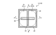
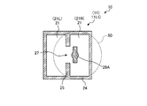
- FIG. 2 is a plan view for explaining an arrangement example of the light receiving pixels 11 and the on-chip lens 50 of the pixel array section 10 according to the first embodiment of the present disclosure.
- 3 is a cross-sectional view taken along the line AA shown in FIG. 2
- FIG. 4 is a cross-sectional view taken along the line BB shown in FIG.
- the pixel array section 10 includes a semiconductor layer 20, a planarization film 30, a color filter 40, and an on-chip lens 50.
- the semiconductor layer 20 contains silicon, for example.
- the semiconductor layer 20 has a plurality of photodiodes (PD) 21 .
- Photodiode 21 is an example of a photoelectric conversion unit.
- One light receiving pixel 11 is provided with a pair of photodiodes 21 (hereinafter also referred to as photodiodes 21L and 21R).
- the light receiving pixel 11 has a substantially square shape in plan view, and the photodiode 21 has a substantially rectangular shape in plan view.
- the photodiode 21 is composed of a first impurity region 22 containing impurities of a first conductivity type (eg, N-type) and a second impurity region 23 containing impurities of a second conductivity type (eg, P-type). .
- the first impurity region 22 is arranged in the central portion of the photodiode 21, and the second impurity region 23 is formed in the side and bottom portions of the first impurity region 22 (parts on the side opposite to the side on which the light L is incident). placed along.
- the light receiving pixel 11 has a first isolation region 24 , a second isolation region 25 , and a third isolation region 26 .
- the first separation region 24 is arranged to surround the pair of photodiodes 21 in one light receiving pixel 11, as shown in FIG.
- the first isolation region 24 is provided so as to penetrate the semiconductor layer 20, as shown in FIGS.
- the first isolation region 24 is made of a low refractive index dielectric such as silicon oxide (SiO 2 ). Thereby, the first isolation region 24 can optically and electrically isolate the plurality of light-receiving pixels 11 adjacent to each other.
- the second isolation region 25 is arranged between a pair of photodiodes 21 adjacent to each other in one light receiving pixel 11, as shown in FIG. Moreover, the second isolation region 25 is provided so as to penetrate the semiconductor layer 20, as shown in FIG.
- the second isolation region 25 is composed of a low refractive index dielectric such as silicon oxide. Thereby, the second isolation region 25 can optically and electrically isolate the plurality of photodiodes 21 adjacent to each other.
- the pair of photodiodes 21 can be separated from each other using the second separation region 25, so that the phase difference of the incident light L is detected using the pair of photodiodes 21. can do.
- the light receiving pixel 11 is provided with the second separation region 25 , the light L incident on the end of the second separation region 25 on the light incident side is greatly scattered due to the large refractive index difference with the photodiode 21 . be done. Then, there is a possibility that color mixture may occur in the pixel array section 10 due to the incident light L that has been largely scattered into another light-receiving pixel 11 .
- the occurrence of such color mixture is particularly conspicuous in another light-receiving pixel 11 adjacent in the direction perpendicular to the direction in which the second isolation region 25 extends (horizontal direction in FIG. 2). That is, the second isolation region 25 may cause uneven color mixture in the plurality of light-receiving pixels 11 arranged around the light-receiving pixels 11 .
- the nonuniformity of color mixture in the pixel array section 10 is improved by providing the third isolation region 26 in the light receiving pixel 11 .
- the third isolation region 26 is arranged in a region surrounded by the first isolation region 24, as shown in FIG. Further, the third separation region 26 is arranged along a direction (horizontal direction in FIG. 2) different from the direction in which the second separation region 25 extends in plan view (vertical direction in FIG. 2).
- the third separation region 26 is provided from the light incident surface 20a of the semiconductor layer 20 to partway through the semiconductor layer 20 (that is, so as not to penetrate the semiconductor layer 20).
- the third isolation region 26 is made of, for example, the same material (dielectric with a low refractive index) as the second isolation region 25 .
- the light L can be scattered in a direction different from that of the second isolation region 25 as well. Therefore, according to the first embodiment, non-uniformity of color mixture in the pixel array section 10 can be improved.
- the third isolation region 26 is preferably provided so as to straddle the second isolation region 25 in plan view.
- a large amount of light L can be scattered in a direction different from that of the second isolation region 25 in a plan view, so that non-uniformity of color mixture in the pixel array section 10 can be further improved.
- the third isolation region 26 may be made of the same material as the first isolation region 24 and the second isolation region 25 (for example, silicon oxide). As a result, the third isolation region 26 can be formed in the same step as the first isolation region 24 and the second isolation region 25 in the manufacturing process of the light receiving pixel 11 to be described later.
- the manufacturing process of the pixel array section 10 can be simplified, so the manufacturing cost of the solid-state imaging device 1 can be reduced.
- the third isolation region 26 may be made of a material different from that of the first isolation region 24 and the second isolation region 25 .
- the third isolation region 26 is made of a material having a higher refractive index than the first isolation region 24 and the second isolation region 25 (for example, tantalum oxide (Ta 2 O 5 ), titanium oxide (TiO 2 ), etc.).
- the degree of scattering of the light L by the third separation region 26 can be variously controlled, so that non-uniformity of color mixture in the pixel array section 10 can be improved.
- the third isolation region 26 is provided so as not to penetrate the semiconductor layer 20 . Thereby, it is possible to prevent the volume of the photodiode 21 from decreasing due to the third isolation region 26 .
- the third isolation region 26 is provided so as not to penetrate the semiconductor layer 20, thereby suppressing electrical isolation of the photodiode 21 by the third isolation region 26. .
- the planarizing film 30 is arranged on the light incident surface 20a of the semiconductor layer 20 to planarize the light incident surface 20a.
- the planarizing film 30 is made of silicon oxide, for example.
- a fixed charge film (not shown) may be arranged between the photodiode 21 and the first isolation region 24, the second isolation region 25, and the planarizing film 30.
- FIG. Such a fixed charge film has a function of fixing charges (here, holes) at the interface between the photodiode 21 and the first isolation region 24 , the second isolation region 25 and the planarizing film 30 .
- Fixed charge films are made of, for example, hafnium oxide (HfO 2 ), aluminum oxide (Al 2 O 3 ), tantalum oxide, zirconium oxide (ZrO 2 ), titanium oxide, magnesium oxide (MgO 2 ), lanthanum oxide (La 2 O 3 ), etc.
- Fixed charge films include praseodymium oxide (Pr 2 O 3 ), cerium oxide (CeO 2 ), neodymium oxide (Nd 2 O 3 ), promethium oxide (Pm 2 O 3 ), samarium oxide (Sm 2 O 3 ), It may be composed of europium oxide (Eu 2 O 3 ) or the like.
- Gd 2 O 3 gadolinium oxide
- Tb 2 O 3 terbium oxide
- Dy 2 O 3 dysprosium oxide
- Ho 2 O 3 holmium oxide
- Er 2 O 3 erbium oxide
- Tm 2 O 3 thulium oxide
- Fixed charge films include ytterbium oxide (Yb 2 O 3 ), lutetium oxide (Lu 2 O 3 ), yttrium oxide (Y 2 O 3 ), aluminum nitride (AlN), hafnium oxynitride (HfON), and aluminum oxynitride film. (AlON) or the like.
- the color filter 40 is an optical filter that transmits light in a predetermined wavelength range of the incident light L, and is provided between the on-chip lens 50 and the planarizing film 30 .
- the on-chip lens 50 is provided on the side of the semiconductor layer 20 on which the light L is incident, and has a function of concentrating the light L toward the corresponding light receiving pixel 11 .
- the on-chip lens 50 is made of, for example, an organic material or silicon oxide.
- one on-chip lens 50 is provided for each light-receiving pixel 11 (that is, one on-chip lens 50 for each pair of photodiodes 21), as shown in FIG.
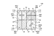
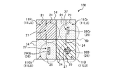
- FIG. 5 is a plan view for explaining an arrangement example of the light receiving pixels 11 and the on-chip lens 50 of the pixel array section 10 according to Modification 1 of the first embodiment of the present disclosure.
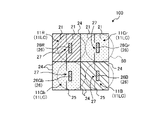
- one light-receiving pixel group 100 is composed of four light-receiving pixels 11 .
- the light receiving pixel group 100 includes a red pixel 11R having a color filter 40R, a green pixel 11Gr having a color filter 40Gr, a green pixel 11Gb having a color filter 40Gb, and a blue pixel 11B having a color filter 40B.
- the color filter 40R is the color filter 40 that transmits light in the red wavelength region of the incident light L, and the color filters 40Gr and 40Gb transmit light in the green wavelength region of the incident light L. It is the color filter 40 . Further, the color filter 40B is a color filter 40 that transmits light in the blue wavelength region of the incident light L. As shown in FIG.
- the color filters 40R, 40Gr, 40Gb, and 40B are arranged in a regular color array (eg, Bayer array).
- the red pixel 11R included in the light-receiving pixel group 100 receives the red light transmitted through the color filter 40R, photoelectrically converts the amount of charge corresponding to the amount of incident red light, and accumulates it inside.
- the green pixels 11Gr and 11Gb receive green light that has passed through the color filters 40Gr and 40Gb, photoelectrically convert the amount of charge corresponding to the amount of incident green light, and store it inside.
- the blue pixel 11B receives the blue light transmitted through the color filter 40B, photoelectrically converts the amount of electric charge corresponding to the amount of incident blue light, and accumulates it inside.
- the individual light-receiving pixels 11 receive light in two or more wavelength regions (three types in the example of FIG. 5).
- the plurality of light receiving pixels 11 included in the same light receiving pixel group 100 have third isolation regions 26 with different shapes.
- the red pixel 11R extends in a direction substantially perpendicular to the second isolation region 25 in a plan view, and also extends from one side of the rectangular first isolation region 24 to the other side. It has a third isolation region 26R arranged at .
- the green pixels 11Gr extend in a direction substantially perpendicular to the second separation region 25 in plan view, and are arranged so as not to extend from one side to the other side of the rectangular first separation region 24 . It has 3 separation regions 26Gr.
- the green pixel 11Gb extends in a direction that obliquely intersects the second separation region 25 from the upper right to the lower left in plan view, and extends from one side to the other side of the rectangular first separation region 24. It has a third isolation region 26Gb arranged so as not to In addition, in the first modification of the first embodiment, the blue pixel 11B is not provided with the third isolation region 26 .
- the plurality of light-receiving pixels 11 included in the same light-receiving pixel group 100 have the third separation regions 26 with various shapes, so that the degree of scattering of the light L by the third separation regions 26 can be variously controlled. can be done. Therefore, according to Modification 1 of the first embodiment, non-uniformity of color mixture in the pixel array section 10 can be improved.
- planar shape of the third separation region 26 arranged in each light receiving pixel 11 is not limited to the example of FIG. 5, and may have various planar shapes.
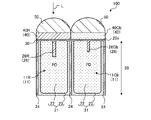
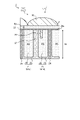
- FIG. 6 is a plan view for explaining an arrangement example of the light receiving pixels 11 and the on-chip lens 50 of the pixel array section 10 according to Modification 2 of the first embodiment of the present disclosure, and FIG. It is a cross-sectional view taken along line CC shown.
- the plurality of light-receiving pixels 11 included in the same light-receiving pixel group 100 have third isolation regions 26 with different shapes.
- the third separation regions 26 provided in one light-receiving pixel 11 are arranged in the same light-receiving pixel group 100 more than the third separation regions 26 provided in different light-receiving pixels 11. may also be formed deeply.
- the third isolation region 26R provided in the red pixel 11R is formed deeper than the third isolation region 26Gb provided in the green pixel 11Gb.
- the plurality of light receiving pixels 11 included in the same light receiving pixel group 100 have the third separation regions 26 with various depths, thereby variously controlling the degree of scattering of the light L by the third separation regions 26. be able to. Therefore, according to Modification 2 of the first embodiment, non-uniformity of color mixture in the pixel array section 10 can be improved.
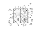
- FIG. 8 is a plan view for explaining an arrangement example of the light receiving pixels 11 and the on-chip lens 50 of the pixel array section 10 according to Modification 3 of the first embodiment of the present disclosure.
- the second isolation region 25 faces in the left-right direction in plan view in the light-receiving pixel 11 .
- the third separation region 26 is arranged along a direction different from the direction in which the second separation region 25 extends in plan view. As a result, the light L can be scattered in a direction different from that of the second separation region 25, so that non-uniformity of color mixture in the pixel array section 10 can be improved.
- the plurality of light-receiving pixels 11 included in the same light-receiving pixel group 100 preferably have third isolation regions 26 with different shapes.
- the red pixel 11R extends in a direction substantially perpendicular to the second isolation region 25 in plan view (vertical direction in FIG. 8), and one side of the rectangular first isolation region 24 It has a third separation region 26R arranged to extend from the side to the other side.
- the green pixel 11Gb extends in a direction substantially perpendicular to the second isolation region 25 in a plan view (vertical direction in FIG. 8), and also extends from one side to the other side of the rectangular first isolation region 24. It has a third isolation region 26Gb which is arranged so as not to
- the green pixel 11Gr extends in a direction that obliquely intersects the second separation region 25 from the upper left to the lower right in a plan view, and extends from one side to the other side of the rectangular first separation region 24. It has a third isolation region 26Gr arranged so as not to extend. In addition, in the third modification of the first embodiment, the blue pixel 11B is not provided with the third isolation region 26 .
- the plurality of light-receiving pixels 11 included in the same light-receiving pixel group 100 have the third separation regions 26 with various shapes, so that the degree of scattering of the light L by the third separation regions 26 can be variously controlled. can be done. Therefore, according to Modification 3 of the first embodiment, the non-uniformity of color mixture in the pixel array section 10 can be further improved.
- planar shape of the third isolation region 26 arranged in each light receiving pixel 11 is not limited to the example in FIG. 8, and may have various planar shapes.
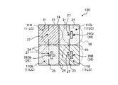
- FIG. 9 is a plan view for explaining an arrangement example of the light receiving pixels 11 and the on-chip lens 50 of the pixel array section 10 according to Modification 4 of the first embodiment of the present disclosure.
- one light-receiving pixel group 100 is composed of 16 light-receiving pixels 11 .
- four green pixels 11Gr1 to 11Gr4 are arranged in two rows and two columns on the upper left of the light receiving pixel group 100 in plan view.
- Four red pixels 11R1 to 11R4 are arranged in two rows and two columns on the upper right side of the light receiving pixel group 100 in plan view.
- four blue pixels 11B1 to 11B4 are arranged in two rows and two columns at the lower left of the light receiving pixel group 100 in plan view.
- four green pixels 11Gb1 to 11Gb4 are arranged in two rows and two columns at the bottom right of the light receiving pixel group 100 in plan view.
- a plurality of light-receiving pixels 11 that are included in the same light-receiving pixel group 100 and that receive light of the same color separate third isolation regions 26 having different shapes from each other. have.
- the green pixels 11Gr1 and 11Gr2 extend in a direction substantially perpendicular to the second separation region 25 in a plan view, and a third separation region arranged to cross the green pixels 11Gr1 and 11Gr2. 26Gr1.
- the red pixel 11R1 extends in a direction that obliquely crosses the second separation region 25 from the upper left to the lower right in a plan view, and the rectangular first separation region 24 extends from one side to the other side. It has a third isolation region 26R1 arranged so as not to extend.
- the red pixel 11R2 extends in a direction that obliquely intersects the second separation region 25 from the upper right to the lower left in plan view, and extends from one side to the other side of the rectangular first separation region 24. It has a third isolation region 26R2 that is arranged so that it does not.
- the red pixel 11R3 extends in a direction that obliquely intersects the second separation region 25 from the upper right to the lower left in plan view, and extends from one side to the other side of the rectangular first separation region 24. It has a third isolation region 26R3 that is arranged so that it does not.
- the red pixel 11R4 extends in a direction that obliquely crosses the second separation region 25 from the upper left to the lower right in plan view, and extends from one side to the other side of the rectangular first separation region 24. It has a third isolation region 26R4 arranged so as not to extend.
- the blue pixel 11B2 extends in a direction substantially perpendicular to the second separation region 25 in plan view (horizontal direction in FIG. 9) and does not extend from one side of the rectangular first separation region 24 to the other side. It has a third isolation region 26B2 arranged as follows.
- the blue pixel 11B3 extends in a direction substantially perpendicular to the second isolation region 25 in plan view (horizontal direction in FIG. 9), and does not extend from one side of the rectangular first isolation region 24 to the other side. It has a third isolation region 26B3 arranged as follows.
- the green pixels 11Gb3 and 11Gb4 have a third isolation region 26Gb3 that extends in a direction substantially perpendicular to the second isolation region 25 in plan view and that is arranged to cross the green pixels 11Gb3 and 11Gb4.
- the plurality of light-receiving pixels 11 included in the same light-receiving pixel group 100 and receiving light of the same color have the third separation regions 26 of various shapes. can be controlled in various ways. Therefore, according to Modification 4 of the first embodiment, the non-uniformity of color mixture in the pixel array section 10 can be further improved.
- planar shape of the third separation region 26 arranged in each light receiving pixel 11 is not limited to the example in FIG. 9, and may have various planar shapes.
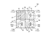
- FIG. 10 is a plan view for explaining an arrangement example of each light receiving pixel 11 and the third isolation region 26 of the pixel array section 10 according to Modification 5 of the first embodiment of the present disclosure.
- the light-receiving pixel 11CC located in the central portion and the light-receiving pixel 11 located in the end portion have an on-chip lens.
- the incident angles of the light L from 50 are different.
- the light scattering state due to the third isolation region 26 differs from that in the light receiving pixels 11CC located in the central portion. That is, in the pixel array section 10 , the light scattering state by the third separation regions 26 differs in the light receiving pixels 11 having different image heights.
- image height refers to the distance from the optical axis (for example, the center of the pixel array section 10).
- the center is expressed as, for example, “low image height” or “center of image height”. It is expressed as "image height”.
- the position and shape of the third isolation region 26 are changed according to the image height of the light receiving pixels 11 on the pixel array section 10 .
- third isolation regions 26 having at least one of different positions and shapes are arranged in a plurality of light-receiving pixels 11 having different image heights.
- the light-receiving pixel 11CC at the image height center has a third separation region 26CC whose center of gravity is arranged at a position substantially equal to the center of gravity of the light-receiving pixel 11CC.
- the light-receiving pixel 11RU located at the upper right end of the pixel array section 10 has a third isolation region 26RU whose center of gravity is located at a position shifted to the lower left from the center of gravity of the light-receiving pixel 11RU.
- the light receiving pixel 11CU positioned at the end of the upper center of the pixel array section 10 has a third isolation region 26CU whose center of gravity is arranged at a position shifted downward from the center of gravity of the light receiving pixel 11CU.
- the light-receiving pixel 11LD positioned at the lower left end of the pixel array section 10 has a third isolation region 26LC whose center of gravity is located at a position shifted to the upper right from the center of gravity of the light-receiving pixel 11LD.
- the third separation regions 26 having mutually different positions in the plurality of light receiving pixels 11 having different image heights, the degree of scattering of the light L by the third separation regions 26 can be variously controlled. be able to. Therefore, according to Modification 5 of the first embodiment, the non-uniformity of color mixture in the pixel array section 10 can be further improved.
- FIG. 10 shows an example in which the position of the third separation region 26 is changed according to the image height on the pixel array section 10, the third separation region 26 according to the image height on the pixel array section 10 is shown.
- the shape of the region 26 may be changed, or both the position and shape of the third isolation region 26 may be changed.
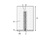
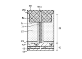
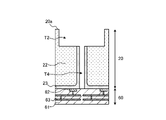
- FIG. 11 to 18 are diagrams showing an example of the manufacturing process of the light receiving pixel 11 according to the first embodiment of the present disclosure.
- a trench T1 is formed on one main surface 20b side of the semiconductor layer 20 containing impurities of the first conductivity type by a conventionally known method. Then, impurities of the second conductivity type are diffused by a conventionally known technique through the inner wall surface of trench T1 and main surface 20b.
- first impurity region 22 and a second impurity region 23 are formed inside the semiconductor layer 20 .
- this trench T1 is formed at a portion where the first isolation region 24 and the second isolation region 25 are provided.
- an oxide film 71 is formed on the inner wall surface of the trench T1 by a conventionally known method, and a polysilicon film 72 is formed by a conventionally known method so as to fill the remaining space of the trench T1.
- a wiring layer 60 is formed on the main surface 20b of the semiconductor layer 20. Then, as shown in FIG. 12, a wiring layer 60 is formed on the main surface 20b of the semiconductor layer 20. Then, as shown in FIG. The wiring layer 60 is configured by providing a plurality of pixel transistors 62 and a plurality of wiring films 63 in an interlayer insulating film 61, and is formed by a conventionally known method.
- the surface of the semiconductor layer 20 opposite to the principal surface 20b is ground to reduce the thickness of the semiconductor layer 20 so that the oxide film 71 and the polysilicon film 72 are exposed. . Thereby, a light incident surface 20 a is formed on the semiconductor layer 20 .
- a trench T2 is formed by a conventionally known method in a portion of the light incident surface 20a of the semiconductor layer 20 where the third isolation region 26 is provided.
- the etching process for forming the trench T2 is performed under the condition that the selection ratio between silicon and oxide film is low.
- a mask M1 is formed by a conventionally known method so as to cover the light incident surface 20a of the semiconductor layer 20 and the trenches T2.
- An opening M1a is formed in the mask M1 so that the polysilicon film 72 is exposed.
- the polysilicon film 72 is etched by a conventionally known technique through the opening M1a of the mask M1. As a result, a trench T3 is formed in the portion of the semiconductor layer 20 where the polysilicon film 72 was formed.
- the mask M1 is removed by a conventionally known technique, and the oxide film 71 is etched by a conventionally known technique. As a result, a trench T4 is formed in the portion of the semiconductor layer 20 where the oxide film 71 and the polysilicon film 72 were formed.
- a fixed charge film (not shown) is formed on the inner wall surfaces of the trenches T2 and T4 by a conventionally known method, and further fills the remaining spaces of the trenches T2 and T4.
- a silicon oxide film is formed by a conventionally known technique.
- the silicon oxide film provided in the trench T2 constitutes the third isolation region 26, and the silicon oxide film provided in the trench T4 constitutes the second isolation region 25.
- the third isolation region 26 can be formed in the same process as the second isolation region 25 . Also, although detailed description is omitted, the first isolation region 24 can also be formed in the same process as the second isolation region 25 .
- the third isolation region 26 can be formed in the same process as the first isolation region 24 and the second isolation region 25 in the manufacturing process of the light receiving pixel 11 .
- the manufacturing process of the pixel array section 10 can be simplified, so the manufacturing cost of the solid-state imaging device 1 can be reduced.
- the second impurity regions 23 can be formed not only on the bottoms of the first impurity regions 22 but also on the sides thereof. can be done.
- the saturation signal charge amount of the photodiode 21 can be increased.
- the impurity region can function as an overflow path.
- the same obliquely incident light passes through an impurity region provided between the pair of photodiodes and passes through the pair of photodiodes. It may be incident on both.
- FIG. FIG. 19 is a plan view for explaining an arrangement example of each light receiving pixel 11 of the pixel array section 10 according to the second embodiment of the present disclosure.
- the pixel array section 10 includes a light receiving pixel 11CC positioned at the image height center, a light receiving pixel 11LC positioned at the left center end, and a light receiving pixel 11LC positioned at the upper center end. and a light receiving pixel 11LU positioned at the upper left end.
- FIG. 20 is a plan view for explaining an arrangement example of the light receiving pixels 11 and the on-chip lens 50 of the pixel array section 10 according to the second embodiment of the present disclosure, and FIG. It is an arrow directional cross-sectional view of a line.
- FIGS. 20 and 21 show an embodiment of the light receiving pixel 11LC located at the left center end portion among the plurality of light receiving pixels 11 provided in the pixel array section 10.
- FIG. 20 and 21 show an embodiment of the light receiving pixel 11LC located at the left center end portion among the plurality of light receiving pixels 11 provided in the pixel array section 10.
- the pixel array section 10 includes a semiconductor layer 20, a planarizing film 30, a color filter 40, and an on-chip lens 50.
- the semiconductor layer 20 contains silicon, for example.
- the semiconductor layer 20 has a plurality of photodiodes (PD) 21 .
- Photodiode 21 is an example of a photoelectric conversion unit.
- One light receiving pixel 11 is provided with a pair of photodiodes 21 (hereinafter also referred to as photodiodes 21L and 21R).
- the light receiving pixel 11 has a substantially square shape in plan view, and the photodiode 21 has a substantially rectangular shape in plan view.
- the photodiode 21 is composed of a first impurity region 22 containing impurities of a first conductivity type (eg, N-type) and a second impurity region 23 containing impurities of a second conductivity type (eg, P-type). .
- the first impurity region 22 is arranged in the central portion of the photodiode 21, and the second impurity region 23 is formed in the side and bottom portions of the first impurity region 22 (parts on the side opposite to the side on which the light L is incident). placed along.
- the light receiving pixel 11 has a first isolation region 24 , a second isolation region 25 , and a third isolation region 26 .
- the first isolation region 24 is arranged to surround the pair of photodiodes 21 in one light receiving pixel 11, as shown in FIG.
- the first isolation region 24 is provided so as to penetrate the semiconductor layer 20, as shown in FIG.
- the first isolation region 24 is made of a low refractive index dielectric such as silicon oxide. Thereby, the first isolation region 24 can optically and electrically isolate the plurality of light-receiving pixels 11 adjacent to each other.
- the second separation region 25 is arranged between a pair of photodiodes 21 adjacent to each other in one light receiving pixel 11, as shown in FIG. Also, the second isolation region 25 is provided so as to penetrate the semiconductor layer 20 in the same manner as the first isolation region 24 .
- the second isolation region 25 is composed of a low refractive index dielectric such as silicon oxide. Thereby, the second isolation region 25 can optically and electrically isolate the plurality of photodiodes 21 adjacent to each other.
- the phase difference of the incident light L is detected using the pair of photodiodes 21. can do.
- the light-receiving pixel 11LC is arranged between the pair of photodiodes 21 at a position different from the second isolation region 25 in a plan view, and is the second impurity region containing the impurity of the second conductivity type. 27.
- the second impurity region 27 is an example of an impurity region.
- the second impurity region 27 functions as an overflow path between the photodiodes 21L and 21R. As a result, in the second embodiment, the amount of charge accumulated in both photodiodes 21L and 21R can be equalized.
- FIG. 22 is a cross-sectional view for explaining the state of the light L incident on the light receiving pixel 11LC in the reference example of the present disclosure.
- the same obliquely incident light L may enter both the photodiodes 21L and 21R via the second impurity region 27 .
- the problem is solved by providing the third separation region 26 for the light receiving pixels 11LC arranged in the high image height region. I decided to
- the third isolation region 26 is arranged in a region surrounded by the first isolation region 24, as shown in FIG.
- the third separation region 26 is located at a position (for example, a position closer to the center of the image height with respect to the second impurity region 27) that can block the light L that is obliquely incident on the second impurity region 27. placed.
- the third isolation region 26 extends along the same direction (vertical direction in FIG. 20) as the direction in which the second isolation region 25 extends, and is arranged adjacent to the second impurity region 27 in plan view.
- the third isolation region 26 is provided from the light incident surface 20a of the semiconductor layer 20 to the middle of the semiconductor layer 20 (that is, so as not to penetrate the semiconductor layer 20), as in the first embodiment described above.
- the third isolation region 26 is made of, for example, the same material (dielectric with a low refractive index) as the second isolation region 25 .
- FIG. 23 is a cross-sectional view for explaining the state of light L incident on the light receiving pixel 11LC according to the second embodiment of the present disclosure.
- the isolation ratio between the pair of photodiodes 21 can be improved.
- the third isolation region 26 may be made of the same material as the first isolation region 24 and the second isolation region 25 (for example, silicon oxide). As a result, the third isolation region 26 can be formed in the same process as the first isolation region 24 and the second isolation region 25 in the manufacturing process of the light receiving pixel 11 .
- the manufacturing process of the pixel array section 10 can be simplified, so the manufacturing cost of the solid-state imaging device 1 can be reduced.
- the third isolation region 26 may be made of a material different from that of the first isolation region 24 and the second isolation region 25 .
- the third isolation region 26A may be made of a material having a higher refractive index than the first isolation region 24 and the second isolation region 25 (eg, tantalum oxide, titanium oxide, etc.).
- FIG. 24 is a plan view for explaining another arrangement example of the light receiving pixels 11LC and the on-chip lens 50 of the pixel array section 10 according to the second embodiment of the present disclosure.
- the difference in refractive index between the third separation region 26A and the photodiode 21 can be reduced, thereby suppressing large scattering of the light L that has entered the end of the third separation region 26A on the light incident side. can do.
- the second embodiment it is possible to suppress the scattered light caused by the third separation region 26A from leaking into another photodiode 21, thereby suppressing the occurrence of color mixture due to such scattered light. can.
- planar arrangement of the third separation regions 26A using a material with a high refractive index is not limited to the example of FIG. 25 and 26 are plan views for explaining another arrangement example of the light receiving pixels 11LC and the on-chip lens 50 of the pixel array section 10 according to the second embodiment of the present disclosure.
- the third isolation region 26A may be divided into two, and as shown in FIG. It may have a shape that expands more than both ends.
- the planarizing film 30 is arranged on the light incident surface 20a of the semiconductor layer 20 to planarize the light incident surface 20a.
- the planarizing film 30 is made of silicon oxide, for example.
- a fixed charge film (not shown) may be arranged between the photodiode 21 and the first isolation region 24 , the second isolation region 25 and the planarization film 30 .
- Such a fixed charge film has a function of fixing charges (here, holes) at the interface between the photodiode 21 and the first isolation region 24 , the second isolation region 25 and the planarizing film 30 .
- the material for the fixed charge film it is preferable to use a high dielectric material with many fixed charges.
- the same material as that of the fixed charge film according to the first embodiment can be used.
- the color filter 40 is an optical filter that transmits light in a predetermined wavelength range of the incident light L, and is provided between the on-chip lens 50 and the planarizing film 30 .
- the on-chip lens 50 is provided on the side of the semiconductor layer 20 on which the light L is incident, and has a function of concentrating the light L toward the corresponding light receiving pixel 11 .
- the on-chip lens 50 is made of, for example, an organic material or silicon oxide.
- one on-chip lens 50 is provided for each light receiving pixel 11 (ie, one on-chip lens 50 for each pair of photodiodes 21).
- the color filter 40 and the on-chip lens 50 are arranged at positions closer to the image height center side than the corresponding pair of photodiodes 21 .
- FIG. 27 is a plan view for explaining an arrangement example of the light receiving pixels 11 and the on-chip lens 50 of the pixel array section 10 according to Modification 1 of the second embodiment of the present disclosure.
- FIG. 27 shows an embodiment of the light-receiving pixel 11LC located at the left center end portion among the plurality of light-receiving pixels 11 provided in the pixel array section 10, as in the second embodiment described above.
- one light-receiving pixel group 100 is composed of four light-receiving pixels 11LC.
- the light-receiving pixel group 100 includes red pixels 11R, green pixels 11Gr, green pixels 11Gb, and blue pixels 11B.
- the red pixel 11R has a color filter 40R (see FIG. 5)
- the green pixels 11Gr and 11Gb have color filters 40Gr and 40Gb (see FIG. 5)
- the blue pixel 11B has a color filter 40B (see FIG. 5). .
- the color filter 40R is the color filter 40 that transmits light in the red wavelength region of the incident light L, and the color filters 40Gr and 40Gb transmit light in the green wavelength region of the incident light L.
- the color filter 40B which is the color filter 40, is a color filter 40 that transmits light in the blue wavelength region of the incident light L. As shown in FIG.
- the color filters 40R, 40Gr, 40Gb, and 40B are arranged in a regular color array (eg, Bayer array).
- the red pixel 11R included in the light-receiving pixel group 100 receives the red light transmitted through the color filter 40R, photoelectrically converts the amount of charge corresponding to the amount of incident red light, and accumulates it inside.
- the green pixels 11Gr and 11Gb receive green light that has passed through the color filters 40Gr and 40Gb, photoelectrically convert the amount of charge corresponding to the amount of incident green light, and store it inside.
- the blue pixel 11B receives the blue light transmitted through the color filter 40B, photoelectrically converts the amount of electric charge corresponding to the amount of incident blue light, and accumulates it inside.
- the individual light-receiving pixels 11 receive light in two or more wavelength regions (three types in the example of FIG. 27).
- the red pixel 11R has a third isolation region 26R
- the green pixels 11Gr and 11Gb have third isolation regions 26Gr and 26Gb
- the blue pixel 11B has a third isolation region 26B.
- the separation ratio between the pair of photodiodes 21 can be improved in all such light receiving pixels 11LC.
- FIG. 28 is a plan view for explaining an arrangement example of the light receiving pixels 11 and the on-chip lens 50 of the pixel array section 10 according to Modification 2 of the second embodiment of the present disclosure.
- FIG. 28 shows the embodiment of the light-receiving pixel 11LC located at the left center end portion among the plurality of light-receiving pixels 11 provided in the pixel array section 10, as in the above-described second embodiment and modification 1. showing. Further, in Modification 2 of the second embodiment, one light-receiving pixel group 100 is composed of four light-receiving pixels 11LC, as in Modification 1 described above.
- the red pixel 11R is not provided with the third isolation region 26 .
- the light in the red wavelength region incident on the red pixel 11R is greatly scattered by the third separation region 26 compared to the light in the green or blue wavelength region, and color mixture due to this scattered light occurs to some extent. .
- the occurrence of color mixture can be suppressed by not providing the third isolation region 26 in the red pixel 11R. Further, in this modified example 2, since the third isolation regions 26 are provided in the green pixels 11Gr and 11Gb and the blue pixels 11B, the isolation ratio between the pair of photodiodes 21 in the green pixels 11Gr and 11Gb and the blue pixels 11B is can be improved.
- Modification 2 of the second embodiment it is possible to achieve both suppression of color mixing and improvement of the separation ratio.
- FIG. 29 is a plan view for explaining an arrangement example of the light receiving pixels 11 and the on-chip lens 50 of the pixel array section 10 according to Modification 3 of the second embodiment of the present disclosure.
- one light-receiving pixel group 100 is composed of four light-receiving pixels 11LC, similarly to Modifications 1 and 2 described above.
- the planar shape of the third isolation region 26B provided in the blue pixel 11B is different from that in Modification 2 described above. Specifically, the third isolation region 26B provided in the blue pixel 11B has a substantially cross shape in plan view.
- the third separation region 26B has a portion that extends in the same direction as the second separation region 25 extends in plan view (vertical direction in FIG. 29) and a portion that extends in a direction different from the direction in which the second separation region 25 extends 29 has a portion extending in the left-right direction).
- the saturation signal charge amount of the blue pixel 11B can be increased.
- the blue pixel 11B and the green pixels 11Gr and 11Gb are provided with the third separation regions 26, while the red pixel 11R is not provided with the third separation region 26. .
- the red pixel 11R is not provided with the third separation region 26.
- FIG. 30 is a plan view for explaining an arrangement example of the light receiving pixels 11 and the on-chip lens 50 of the pixel array section 10 according to Modification 4 of the second embodiment of the present disclosure.
- one light-receiving pixel group 100 is composed of four light-receiving pixels 11LC, similarly to Modifications 1 to 3 described above.
- the planar shape of the third separation regions 26Gr provided in the green pixels 11Gr and 11Gb is different from that in Modification 3 described above.
- the third isolation regions 26Gr and 26Gb provided in the green pixels 11Gr and 11Gb have a substantially cross shape in plan view.
- the saturation signal charge amount of the green pixels 11Gr and 11Gb can be increased.
- the cross-shaped third isolation region 26B is provided in the blue pixel 11B, so that the saturation signal charge amount of the blue pixel 11B can also be increased.
- the blue pixel 11B and the green pixels 11Gr and 11Gb are provided with the third separation regions 26, while the red pixel 11R is not provided with the third separation region 26. .
- the red pixel 11R is not provided with the third separation region 26.
- FIG. 31 is a plan view for explaining an arrangement example of the light receiving pixels 11 and the on-chip lens 50 of the pixel array section 10 according to Modification 5 of the second embodiment of the present disclosure.
- the light-receiving pixel 11LU positioned at the upper left end is an embodiment. is shown.
- one light-receiving pixel group 100 is composed of four light-receiving pixels 11LU.
- the light-receiving pixel group 100 includes red pixels 11R, green pixels 11Gr, green pixels 11Gb, and blue pixels 11B.
- the red pixel 11R has a color filter 40R (see FIG. 5)
- the green pixels 11Gr and 11Gb have color filters 40Gr and 40Gb (see FIG. 5)
- the blue pixel 11B has a color filter 40B (see FIG. 5). .
- the individual light-receiving pixels 11 receive light in two or more (three in the example of FIG. 31) wavelength regions.
- the third isolation region 26 according to Modification 5 of the second embodiment is located at a position where it can block the light L that obliquely enters the second impurity region 27 (e.g. position closer to the center of the image height than the
- the image height center is arranged at the lower right of the light receiving pixel group 100 in plan view. It is placed in a position closer to the lower right side.
- the third separation region 26 extends along the same direction as the direction in which the second separation region 25 extends (vertical direction in FIG. 31).
- the same light L passes through the second impurity region 27 to form a pair of photodiodes in all the light receiving pixels 11LU. 21 can be suppressed.
- FIG. 32 is a plan view for explaining an arrangement example of the light receiving pixels 11 and the on-chip lens 50 of the pixel array section 10 according to Modification 6 of the second embodiment of the present disclosure.
- FIG. 32 shows an embodiment of the light-receiving pixel 11LU positioned at the upper left end of the plurality of light-receiving pixels 11 provided in the pixel array section 10, as in the fifth modification of the second embodiment described above. ing. Further, in Modification 2 of the second embodiment, one light-receiving pixel group 100 is composed of four light-receiving pixels 11LU, as in Modification 5 described above.
- the red pixel 11R is not provided with the third isolation region 26 .
- the light in the red wavelength region incident on the red pixel 11R is greatly scattered by the third separation region 26 compared to the light in the green or blue wavelength region, and color mixture due to this scattered light occurs to some extent. do.
- Modification 6 the occurrence of color mixture can be suppressed by not providing the third isolation region 26 in the red pixel 11R.
- the third isolation region 26 is provided in the green pixels 11Gr and 11Gb and the blue pixel 11B, the isolation ratio between the pair of photodiodes 21 in the green pixels 11Gr and 11Gb and the blue pixel 11B is can be improved.
- Modification 6 of the second embodiment it is possible to achieve both suppression of color mixing and improvement of the separation ratio.
- FIG. 33 is a plan view for explaining an arrangement example of the light receiving pixels 11 and the on-chip lens 50 of the pixel array section 10 according to Modification 7 of the second embodiment of the present disclosure.
- one light-receiving pixel group 100 is composed of four light-receiving pixels 11LU, as in Modifications 5 and 6 described above.
- the planar shape of the third isolation region 26B provided in the blue pixel 11B is different from that in Modification 6 described above. Specifically, the third isolation region 26B provided in the blue pixel 11B has a substantially cross shape in plan view.
- the saturation signal charge amount of the blue pixel 11B can be increased.
- the blue pixel 11B and the green pixels 11Gr and 11Gb are provided with the third separation regions 26, while the red pixel 11R is not provided with the third separation region 26. .
- the red pixel 11R is not provided with the third separation region 26.
- FIG. 34 is a plan view for explaining an arrangement example of the light receiving pixels 11 and the on-chip lens 50 of the pixel array section 10 according to Modification 8 of the second embodiment of the present disclosure.
- one light-receiving pixel group 100 is composed of four light-receiving pixels 11LU, as in Modifications 5 to 7 described above.
- the planar shape of the third separation regions 26Gr provided in the green pixels 11Gr and 11Gb is different from that in Modification 7 described above.
- the third isolation regions 26Gr and 26Gb provided in the green pixels 11Gr and 11Gb have a substantially cross shape in plan view.
- the saturation signal charge amount of the green pixels 11Gr and 11Gb can be increased.
- the blue pixel 11B is provided with the cross-shaped third isolation region 26B, so that the saturation signal charge amount of the blue pixel 11B can also be increased.
- the blue pixel 11B and the green pixels 11Gr and 11Gb are provided with the third separation regions 26, while the red pixel 11R is not provided with the third separation region 26. .
- the red pixel 11R is not provided with the third separation region 26.
- FIG. 35 is a plan view for explaining an arrangement example of the light receiving pixels 11 and the on-chip lens 50 of the pixel array section 10 according to Modification 9 of the second embodiment of the present disclosure.
- one light-receiving pixel group 100 is composed of four light-receiving pixels 11CU.
- the light-receiving pixel group 100 includes red pixels 11R, green pixels 11Gr, green pixels 11Gb, and blue pixels 11B.
- the red pixel 11R has a color filter 40R (see FIG. 5)
- the green pixels 11Gr and 11Gb have color filters 40Gr and 40Gb (see FIG. 5)
- the blue pixel 11B has a color filter 40B (see FIG. 5). .
- the individual light-receiving pixels 11 receive light in two or more (three in the example of FIG. 35) wavelength regions.
- the ninth modification of the second embodiment as shown in FIG. 35, all the light receiving pixels 11CU included in the same light receiving pixel group 100 are arranged in the third separation region so as to overlap the second impurity region 27. 26.
- the third separation region 26 extends along a direction (diagonal direction in FIG. 35) crossing the direction in which the second separation region 25 extends.
- the image height center is arranged below the light receiving pixel group 100 in plan view, so that the obliquely incident light L passes through the second impurity region 27. Therefore, it is basically impossible for the light to enter both of the pair of photodiodes 21 .
- the separation ratio between the pair of photodiodes 21 can be improved in all the light receiving pixels 11CU.
- planar shape of the third isolation region 26 arranged in the light receiving pixel 11 is not limited to the example of the present disclosure, and various planar shapes may be used. good.
- the solid-state imaging device 1 includes a plurality of light receiving pixels 11 arranged in a matrix inside a semiconductor layer 20 .
- the light-receiving pixel 11 also has a pair of photoelectric conversion portions (photodiodes 21 ), a first isolation region 24 , a second isolation region 25 , and a third isolation region 26 .
- a pair of photoelectric conversion units (photodiodes 21) are arranged adjacent to each other.
- the first isolation region 24 is arranged so as to surround the pair of photoelectric conversion units (photodiodes 21 ) and is provided so as to penetrate the semiconductor layer 20 .
- the second separation region 25 is arranged between a pair of photoelectric conversion units (photodiodes 21 ) and is provided so as to penetrate the semiconductor layer 20 .
- the third isolation region 26 is arranged in a region surrounded by the first isolation region 24 and provided from the light incident surface 20a of the semiconductor layer 20 to the middle of the semiconductor layer 20 .
- the third isolation region 26 is provided so as to straddle the second isolation region 25 in plan view.
- the solid-state imaging device 1 includes a light-receiving pixel group 100 having a plurality of light-receiving pixels 11 that receive light in two or more wavelength regions. Further, the plurality of light-receiving pixels 11 included in the same light-receiving pixel group 100 are provided with third isolation regions 26 having at least one of different positions and shapes.
- the third isolation regions 26 having at least one of different positions and shapes are arranged in the plurality of light receiving pixels 11 having different image heights.
- the solid-state imaging device 1 includes a plurality of light receiving pixels 11 arranged in a matrix inside the semiconductor layer 20 .
- the light receiving pixel 11 includes a pair of photoelectric conversion portions (photodiodes 21), a first isolation region 24, a second isolation region 25, an impurity region (second impurity region 27), and a third isolation region 26.
- a pair of photoelectric conversion units (photodiodes 21) are arranged adjacent to each other.
- the first isolation region 24 is arranged so as to surround the pair of photoelectric conversion units (photodiodes 21 ) and is provided so as to penetrate the semiconductor layer 20 .
- the second separation region 25 is arranged between a pair of photoelectric conversion units (photodiodes 21 ) and is provided so as to penetrate the semiconductor layer 20 .
- the impurity region (second impurity region 27) is arranged at a position different from that of the second separation region 25 in plan view between the pair of photoelectric conversion portions (photodiodes 21).
- the third isolation region 26 is arranged in a region surrounded by the first isolation region 24 and provided from the light incident surface 20a of the semiconductor layer 20 to the middle of the semiconductor layer 20 .
- the third isolation region 26 is arranged adjacent to the impurity region (second impurity region 27) in plan view.
- the third isolation region 26 has a substantially cross shape in plan view.
- the third isolation regions 26 having at least one of different positions and shapes are arranged in the plurality of light receiving pixels 11 having different image heights.
- the present disclosure is not limited to application to solid-state imaging devices. That is, the present disclosure applies to general electronic devices having a solid-state imaging device, such as a camera module, an imaging device, a mobile terminal device having an imaging function, or a copier using a solid-state imaging device as an image reading unit, in addition to the solid-state imaging device. applicable.
- a solid-state imaging device such as a camera module, an imaging device, a mobile terminal device having an imaging function, or a copier using a solid-state imaging device as an image reading unit, in addition to the solid-state imaging device.
- imaging devices examples include digital still cameras and video cameras.
- Mobile terminal devices having such an imaging function include, for example, smartphones and tablet terminals.
- FIG. 36 is a block diagram showing a configuration example of an imaging device as the electronic device 1000 to which the technology according to the present disclosure is applied.
- An electronic device 1000 in FIG. 36 is, for example, an imaging device such as a digital still camera or a video camera, or an electronic device such as a mobile terminal device such as a smart phone or a tablet terminal.
- an electronic device 1000 includes a lens group 1001, a solid-state image sensor 1002, a DSP circuit 1003, a frame memory 1004, a display unit 1005, a recording unit 1006, an operation unit 1007, and a power supply unit 1008. Configured.
- the DSP circuit 1003 , frame memory 1004 , display section 1005 , recording section 1006 , operation section 1007 and power supply section 1008 are interconnected via a bus line 1009 .
- a lens group 1001 captures incident light (image light) from a subject and forms an image on the imaging surface of the solid-state imaging device 1002 .
- the solid-state imaging device 1002 corresponds to the solid-state imaging device 1 according to each of the above-described embodiments, and converts the amount of incident light imaged on the imaging surface by the lens group 1001 into an electric signal on a pixel-by-pixel basis. Output.
- the DSP circuit 1003 is a camera signal processing circuit that processes signals supplied from the solid-state imaging device 1002 .
- a frame memory 1004 temporarily holds the image data processed by the DSP circuit 1003 in frame units.
- a display unit 1005 is composed of a panel-type display device such as a liquid crystal panel or an organic EL (Electro Luminescence) panel, and displays moving images or still images captured by the solid-state imaging device 1002 .
- a recording unit 1006 records image data of a moving image or a still image captured by the solid-state imaging device 1002 in a recording medium such as a semiconductor memory or a hard disk.
- the operation unit 1007 issues operation commands for various functions of the electronic device 1000 in accordance with user's operations.
- a power supply unit 1008 appropriately supplies various power supplies as operating power supplies for the DSP circuit 1003, frame memory 1004, display unit 1005, recording unit 1006, and operation unit 1007 to these supply targets.
- the signal quality can be improved by applying the solid-state imaging device 1 of each embodiment described above as the solid-state imaging device 1002 .
- the present technology can also take the following configuration.
- (1) Equipped with a plurality of light receiving pixels arranged in a matrix inside the semiconductor layer,
- the light-receiving pixels are a pair of photoelectric conversion units arranged adjacent to each other; a first separation region arranged to surround the pair of photoelectric conversion units and penetrating through the semiconductor layer; a second isolation region disposed between the pair of photoelectric conversion units and provided to penetrate the semiconductor layer; a third separation region arranged in a region surrounded by the first separation region, and provided from the light incident surface of the semiconductor layer to the middle of the semiconductor layer.
- (2) The solid-state imaging device according to (1), wherein the third isolation region is provided so as to straddle the second isolation region in plan view.
- a light-receiving pixel group having a plurality of light-receiving pixels that receive light in two or more wavelength regions The solid-state imaging device according to (1) or (2), wherein the third separation regions having at least one of positions and shapes different from each other are arranged in the plurality of light receiving pixels included in the same light receiving pixel group.
- the solid-state imaging device is Having a plurality of light receiving pixels arranged in a matrix inside the semiconductor layer,
- the light-receiving pixels are a pair of photoelectric conversion units arranged adjacent to each other; a first separation region arranged to surround the pair of photoelectric conversion units and penetrating through the semiconductor layer; a second isolation region disposed between the pair of photoelectric conversion units and provided to penetrate the semiconductor layer; and a third separation region arranged in a region surrounded by the first separation region, and provided from the light incident surface of the semiconductor layer to the middle of the semiconductor layer.
- the light-receiving pixels are a pair of photoelectric conversion units arranged adjacent to each other; a first separation region arranged to surround the pair of photoelectric conversion units and penetrating through the semiconductor layer; a second isolation region disposed between the pair of photoelectric conversion units and provided to penetrate the semiconductor layer; an impurity region arranged at a position different from the second isolation region in plan view between the pair of photoelectric conversion units; a third separation region arranged in a region surrounded by the first separation region, and provided from the light incident surface of the semiconductor layer to partway through the semiconductor layer.
- the solid-state imaging device is Having a plurality of light receiving pixels arranged in a matrix inside the semiconductor layer, The light-receiving pixels are a pair of photoelectric conversion units arranged adjacent to each other; a first separation region arranged to surround the pair of photoelectric conversion units and penetrating through the semiconductor layer; a second isolation region disposed between the pair of photoelectric conversion units and provided to penetrate the semiconductor layer; an impurity region arranged at a position different from the second isolation region in plan view between the pair of photoelectric conversion units; and a third separation region arranged in a region surrounded by the first separation region, and provided from the light incident surface of the semiconductor layer to the middle of the semiconductor layer.
Landscapes
- Engineering & Computer Science (AREA)
- Multimedia (AREA)
- Signal Processing (AREA)
- Solid State Image Pick-Up Elements (AREA)
- Transforming Light Signals Into Electric Signals (AREA)
Abstract
本開示に係る固体撮像素子(1)は、半導体層(20)の内部に行列状に配列される複数の受光画素(11)を備える。また、受光画素(11)は、一対の光電変換部と、第1分離領域(24)と、第2分離領域(25)と、第3分離領域(26)と、を有する。一対の光電変換部は、互いに隣接して配置される。第1分離領域(24)は、一対の光電変換部を囲むように配置され、半導体層(20)を貫通するように設けられる。第2分離領域(25)は、一対の光電変換部同士の間に配置され、半導体層(20)を貫通するように設けられる。第3分離領域(26)は、第1分離領域(24)によって囲まれる領域に配置され、半導体層(20)の光入射面(20a)から半導体層(20)の途中まで設けられる。
Description
本開示は、固体撮像素子および電子機器に関する。
近年、裏面照射型のCMOS(Complementary Metal Oxide Semiconductor)イメージセンサにおいて、同じオンチップレンズから一対のフォトダイオードに光を入射させることにより、位相差の検出を実現させる技術がある(たとえば、特許文献1参照)。
しかしながら、上記の従来技術では、同じオンチップレンズから一対のフォトダイオードに光を入射させることにより、入射した光が一対のフォトダイオード同士の間に設けられる分離領域で大きく散乱され、不均一な混色が発生する場合がある。
そこで、本開示では、混色の不均一性を改善することができる固体撮像素子および電子機器を提案する。
本開示によれば、固体撮像素子が提供される。固体撮像素子は、半導体層の内部に行列状に配列される複数の受光画素を備える。また、前記受光画素は、一対の光電変換部と、第1分離領域と、第2分離領域と、第3分離領域と、を有する。一対の光電変換部は、互いに隣接して配置される。第1分離領域は、前記一対の光電変換部を囲むように配置され、前記半導体層を貫通するように設けられる。第2分離領域は、前記一対の光電変換部同士の間に配置され、前記半導体層を貫通するように設けられる。第3分離領域は、前記第1分離領域によって囲まれる領域に配置され、前記半導体層の光入射面から前記半導体層の途中まで設けられる。
以下に、本開示の各実施形態について図面に基づいて詳細に説明する。なお、以下の各実施形態において、同一の部位には同一の符号を付することにより重複する説明を省略する。
近年、裏面照射型のCMOS(Complementary Metal Oxide Semiconductor)イメージセンサにおいて、同じオンチップレンズから一対のフォトダイオードに光を入射させることにより、位相差の検出を実現させる技術がある。
しかしながら、上記の従来技術では、同じオンチップレンズから一対のフォトダイオードに光を入射させることにより、入射した光が一対のフォトダイオード同士の間に設けられる分離領域で大きく散乱する場合がある。そして、この大きく散乱した光が別のフォトダイオードに入射することにより、画素アレイ部内で混色が発生する恐れがある。
また、かかる混色の発生は、分離領域が延びる方向とは垂直な方向に隣接する別のフォトダイオードで特に顕著である。すなわち、上記の従来技術では、一対のフォトダイオードの周囲に配置される複数のフォトダイオードにおいて、混色が不均一に発生する恐れがある。
そこで、上述の問題点を克服し、混色の不均一性を改善することができる技術の実現が期待されている。
[固体撮像素子の構成]
図1は、本開示の各実施形態に係る固体撮像素子1の概略構成例を示すシステム構成図である。図1に示すように、CMOSイメージセンサである固体撮像素子1は、画素アレイ部10と、システム制御部12と、垂直駆動部13と、カラム読出し回路部14と、カラム信号処理部15と、水平駆動部16と、信号処理部17とを備える。
図1は、本開示の各実施形態に係る固体撮像素子1の概略構成例を示すシステム構成図である。図1に示すように、CMOSイメージセンサである固体撮像素子1は、画素アレイ部10と、システム制御部12と、垂直駆動部13と、カラム読出し回路部14と、カラム信号処理部15と、水平駆動部16と、信号処理部17とを備える。
これら画素アレイ部10、システム制御部12、垂直駆動部13、カラム読出し回路部14、カラム信号処理部15、水平駆動部16および信号処理部17は、同一の半導体基板上または電気的に接続された複数の積層半導体基板上に設けられる。
画素アレイ部10には、入射光量に応じた電荷量を光電変換して内部に蓄積し、信号として出力することが可能な光電変換素子(フォトダイオード21(図2参照))を有する受光画素11が行列状に2次元配置されている。
また、画素アレイ部10は、受光画素11の他に、フォトダイオード21を持たない構造のダミー画素や、受光面を遮光することで外部からの光入射が遮断された遮光画素などが、行および/または列状に配置されている領域を含む場合がある。
なお、遮光画素は、受光面が遮光された構造である以外は、受光画素11と同様の構成を備えていてもよい。また、以下では、入射光量に応じた電荷量の光電荷を、単に「電荷」とも呼称し、受光画素11を、単に「画素」とも呼称する場合もある。
画素アレイ部10には、行列状の画素配列に対して、行ごとに画素駆動線LDが図面中の左右方向(画素行の画素の配列方向)に沿って形成され、列ごとに垂直画素配線LVが図面中の上下方向(画素列の画素の配列方向)に沿って形成される。画素駆動線LDの一端は、垂直駆動部13の各行に対応した出力端に接続される。
カラム読出し回路部14は、少なくとも、画素アレイ部10内の選択行における受光画素11に列ごとに定電流を供給する回路、カレントミラー回路および読出し対象となる受光画素11の切替えスイッチなどを含む。
そして、カラム読出し回路部14は、画素アレイ部10内の選択画素におけるトランジスタとともに増幅器を構成し、光電荷信号を電圧信号に変換して垂直画素配線LVに出力する。
垂直駆動部13は、シフトレジスタやアドレスデコーダなどを含み、画素アレイ部10の各受光画素11を、全画素同時や行単位などで駆動する。この垂直駆動部13は、その具体的な構成については図示を省略するが、読出し走査系と、掃出し走査系あるいは一括掃出しおよび一括転送系とを有する構成となっている。
読出し走査系は、受光画素11から画素信号を読み出すために、画素アレイ部10の受光画素11を行単位で順に選択走査する。行駆動(ローリングシャッタ動作)の場合、掃出しについては、読出し走査系によって読出し走査が行われる読出し行に対して、その読出し走査よりもシャッタスピードの時間分だけ先行して掃出し走査が行なわれる。
また、グローバル露光(グローバルシャッタ動作)の場合は、一括転送よりもシャッタスピードの時間分先行して一括掃出しが行なわれる。このような掃出しにより、読出し行の受光画素11のフォトダイオード21から不要な電荷が掃出し(リセット)される。そして、不要電荷の掃出し(リセット)により、いわゆる電子シャッタ動作が行われる。
ここで、電子シャッタ動作とは、直前までフォトダイオード21に溜まっていた不要な光電荷を捨てて、新たに露光を開始する(光電荷の蓄積を開始する)動作のことをいう。
読出し走査系による読出し動作によって読み出される信号は、その直前の読出し動作または電子シャッタ動作以降に入射した光量に対応するものである。行駆動の場合は、直前の読出し動作による読出しタイミングまたは電子シャッタ動作による掃出しタイミングから、今回の読出し動作による読出しタイミングまでの期間が、受光画素11における光電荷の蓄積時間(露光時間)となる。グローバル露光の場合は、一括掃出しから一括転送までの時間が蓄積時間(露光時間)となる。
垂直駆動部13によって選択走査された画素行の各受光画素11から出力される画素信号は、垂直画素配線LVの各々を通してカラム信号処理部15に供給される。カラム信号処理部15は、画素アレイ部10の画素列ごとに、選択行の各受光画素11から垂直画素配線LVを通して出力される画素信号に対して所定の信号処理を行うとともに、信号処理後の画素信号を一時的に保持する。
具体的には、カラム信号処理部15は、信号処理として少なくとも、ノイズ除去処理、たとえばCDS(Correlated Double Sampling:相関二重サンプリング)処理を行う。このカラム信号処理部15によるCDS処理により、リセットノイズや増幅トランジスタAMPの閾値ばらつきなどの画素固有の固定パターンノイズが除去される。
なお、カラム信号処理部15には、ノイズ除去処理以外に、たとえば、AD変換機能を持たせて、画素信号をデジタル信号として出力するように構成することもできる。
水平駆動部16は、シフトレジスタやアドレスデコーダなどを含み、カラム信号処理部15の画素列に対応する単位回路を順番に選択する。この水平駆動部16による選択走査により、カラム信号処理部15で信号処理された画素信号が順番に信号処理部17に出力される。
システム制御部12は、各種のタイミング信号を生成するタイミングジェネレータなどを含み、タイミングジェネレータで生成された各種のタイミング信号を基に、垂直駆動部13、カラム信号処理部15、水平駆動部16などの駆動制御を行う。
固体撮像素子1は、さらに、信号処理部17と、図示しないデータ格納部とを備える。信号処理部17は、少なくとも加算処理機能を有し、カラム信号処理部15から出力される画素信号に対して加算処理などの種々の信号処理を行う。
データ格納部は、信号処理部17での信号処理にあたって、その処理に必要なデータを一時的に格納する。これら信号処理部17およびデータ格納部については、固体撮像素子1とは別の基板に設けられる外部信号処理部、たとえばDSP(Digital Signal Processor)やソフトウェアによる処理であってもよいし、固体撮像素子1と同じ基板上に搭載されてもよい。
[第1実施形態]
つづいて、第1実施形態に係る画素アレイ部10の詳細な構成について、図2~図4を参照しながら説明する。図2は、本開示の第1実施形態に係る画素アレイ部10の受光画素11およびオンチップレンズ50の配置例を説明するための平面図である。また、図3は、図2に示すA-A線の矢視断面図であり、図4は、図2に示すB-B線の矢視断面図である。
つづいて、第1実施形態に係る画素アレイ部10の詳細な構成について、図2~図4を参照しながら説明する。図2は、本開示の第1実施形態に係る画素アレイ部10の受光画素11およびオンチップレンズ50の配置例を説明するための平面図である。また、図3は、図2に示すA-A線の矢視断面図であり、図4は、図2に示すB-B線の矢視断面図である。
図3などに示すように、画素アレイ部10は、半導体層20と、平坦化膜30と、カラーフィルタ40と、オンチップレンズ50とを備える。
半導体層20は、たとえば、シリコンを含む。半導体層20は、複数のフォトダイオード(PD)21を有する。フォトダイオード21は、光電変換部の一例である。なお、1つの受光画素11には、一対のフォトダイオード21(以下、フォトダイオード21L、21Rとも呼称する。)が設けられる。また、受光画素11は平面視で略正方形状であり、フォトダイオード21は平面視で略長方形状である。
フォトダイオード21は、第1導電型(たとえば、N型)の不純物を含む第1不純物領域22と、第2導電型(たとえば、P型)の不純物を含む第2不純物領域23とで構成される。
第1不純物領域22は、フォトダイオード21の中央部に配置され、第2不純物領域23は、かかる第1不純物領域22の側部および底部(光Lが入射する側とは反対側の部位)に沿って配置される。
また、受光画素11は、第1分離領域24と、第2分離領域25と、第3分離領域26とを有する。第1分離領域24は、図2に示すように、1つの受光画素11において一対のフォトダイオード21を囲むように配置される。
また、第1分離領域24は、図3および図4に示すように、半導体層20を貫通するように設けられる。かかる第1分離領域24は、たとえば、酸化シリコン(SiO2)などの低屈折率の誘電体で構成される。これにより、第1分離領域24は、互いに隣接する複数の受光画素11同士の間を光学的および電気的に分離することができる。
第2分離領域25は、図2に示すように、1つの受光画素11において互いに隣接する一対のフォトダイオード21同士の間に配置される。また、第2分離領域25は、図4に示すように、半導体層20を貫通するように設けられる。
かかる第2分離領域25は、たとえば、酸化シリコンなどの低屈折率の誘電体で構成される。これにより、第2分離領域25は、互いに隣接する複数のフォトダイオード21同士の間を光学的および電気的に分離することができる。
このように、第1実施形態では、第2分離領域25を用いて一対のフォトダイオード21同士を互いに分離することができることから、一対のフォトダイオード21を用いて入射する光Lの位相差を検出することができる。
一方で、受光画素11に第2分離領域25が設けられることにより、かかる第2分離領域25における光入射側の端部に入射した光Lは、フォトダイオード21との大きな屈折率差によって大きく散乱される。そして、この大きく散乱した光Lが別の受光画素11に入射することにより、画素アレイ部10内で混色が発生する恐れがある。
また、かかる混色の発生は、第2分離領域25が延びる方向とは垂直な方向(図2では左右方向)に隣接する別の受光画素11で特に顕著である。すなわち、第2分離領域25によって、受光画素11の周囲に配置される複数の受光画素11において、混色が不均一に発生する恐れがある。
そこで、第1実施形態では、受光画素11内に第3分離領域26を設けることにより、画素アレイ部10における混色の不均一性を改善することとした。
具体的には、第3分離領域26は、図2に示すように、第1分離領域24によって囲まれる領域に配置される。また、第3分離領域26は、平面視で第2分離領域25が延びる方向(図2では上下方向)とは異なる方向(図2では左右方向)に沿って配置される。
また、図3および図4に示すように、第3分離領域26は、半導体層20の光入射面20aから半導体層20の途中まで(すなわち、半導体層20を貫通しないように)設けられる。第3分離領域26は、たとえば、第2分離領域25と同じ材料(低屈折率の誘電体)で構成される。
このような第3分離領域26を受光画素11に設けることにより、第2分離領域25とは異なる方向にも光Lを散乱させることができる。したがって、第1実施形態によれば、画素アレイ部10における混色の不均一性を改善することができる。
また、第1実施形態では、第3分離領域26が、平面視で第2分離領域25を跨ぐように設けられるとよい。これにより、平面視で第2分離領域25とは異なる方向に多くの光Lを散乱させることができることから、画素アレイ部10における混色の不均一性をさらに改善することができる。
また、第1実施形態では、第3分離領域26が第1分離領域24および第2分離領域25と同じ材料(たとえば、酸化シリコン)で構成されるとよい。これにより、後述する受光画素11の製造工程において、第3分離領域26を第1分離領域24および第2分離領域25と同じ工程で形成することができる。
したがって、第1実施形態によれば、画素アレイ部10の製造工程を簡素化することができることから、固体撮像素子1の製造コストを低減することができる。
一方で、第1実施形態では、第3分離領域26が第1分離領域24および第2分離領域25と異なる材料で構成されてもよい。たとえば、第3分離領域26が、第1分離領域24および第2分離領域25よりも屈折率の高い材料(たとえば、酸化タンタル(Ta2O5)や酸化チタン(TiO2)など)で構成されてもよい。
これにより、第3分離領域26による光Lの散乱の程度をさまざまに制御することができることから、画素アレイ部10における混色の不均一性を改善することができる。
また、第1実施形態では、第3分離領域26が半導体層20を貫通しないように設けられるとよい。これにより、フォトダイオード21の体積が第3分離領域26によって減少することを抑制することができる。
したがって、第1実施形態によれば、第3分離領域26によってフォトダイオード21の飽和信号電荷量が減少することを抑制することができる。さらに、第1実施形態では、第3分離領域26が半導体層20を貫通しないように設けられることにより、フォトダイオード21が第3分離領域26によって電気的に分離されることを抑制することができる。
画素アレイ部10におけるその他の部位の説明を続ける。平坦化膜30は、半導体層20の光入射面20aに配置され、かかる光入射面20aを平坦化する。平坦化膜30は、たとえば、酸化シリコンで構成される。
なお、第1実施形態では、フォトダイオード21と第1分離領域24、第2分離領域25および平坦化膜30との間に、図示しない固定電荷膜が配置されてもよい。かかる固定電荷膜は、フォトダイオード21と第1分離領域24、第2分離領域25および平坦化膜30との界面に電荷(ここでは、正孔)を固定する機能を有する。
固定電荷膜の材料としては、固定電荷を多く有する高誘電材料を用いることが好ましい。固定電荷膜は、たとえば、酸化ハフニウム(HfO2)、酸化アルミニウム(Al2O3)、酸化タンタル、酸化ジルコニウム(ZrO2)、酸化チタン、酸化マグネシウム(MgO2)、酸化ランタン(La2O3)などで構成される。
また、固定電荷膜は、酸化プラセオジム(Pr2O3)、酸化セリウム(CeO2)、酸化ネオジム(Nd2O3)、酸化プロメチウム(Pm2O3)、酸化サマリウム(Sm2O3)、酸化ユウロピウム(Eu2O3)などで構成されてもよい。
また、固定電荷膜は、酸化ガドリニウム(Gd2O3)、酸化テルビウム(Tb2O3)、酸化ジスプロシウム(Dy2O3)、酸化ホルミウム(Ho2O3)、酸化エルビウム(Er2O3)、酸化ツリウム(Tm2O3)などで構成されてもよい。
また、固定電荷膜は、酸化イッテルビウム(Yb2O3)、酸化ルテチウム(Lu2O3)、酸化イットリウム(Y2O3)窒化アルミニウム(AlN)、酸窒化ハフニウム(HfON)、酸窒化アルミニウム膜(AlON)などで構成されてもよい。
カラーフィルタ40は、入射する光Lのうちの所定の波長領域の光を透過させる光学的なフィルタであり、オンチップレンズ50と平坦化膜30との間に設けられる。
オンチップレンズ50は、半導体層20に対して光Lが入射する側に設けられ、対応する受光画素11に向かって光Lを集光させる機能を有する。オンチップレンズ50は、たとえば、有機材料や酸化シリコンなどで構成される。
第1実施形態では、図2などに示すように、1つの受光画素11ごとに1つのオンチップレンズ50(すなわち、一対のフォトダイオード21ごとに1つのオンチップレンズ50)が設けられる。
[第1実施形態の各種変形例]
つづいて、第1実施形態の各種変形例について、図5~図10を参照しながら説明する。
つづいて、第1実施形態の各種変形例について、図5~図10を参照しながら説明する。
<変形例1>
図5は、本開示の第1実施形態の変形例1に係る画素アレイ部10の受光画素11およびオンチップレンズ50の配置例を説明するための平面図である。
図5は、本開示の第1実施形態の変形例1に係る画素アレイ部10の受光画素11およびオンチップレンズ50の配置例を説明するための平面図である。
第1実施形態の変形例1では、図5に示すように、4つの受光画素11で1つの受光画素群100が構成される。かかる受光画素群100は、カラーフィルタ40Rを有する赤色画素11Rと、カラーフィルタ40Grを有する緑色画素11Grと、カラーフィルタ40Gbを有する緑色画素11Gbと、カラーフィルタ40Bを有する青色画素11Bとを有する。
カラーフィルタ40Rは、入射する光Lのうちの赤色の波長領域の光を透過させるカラーフィルタ40であり、カラーフィルタ40Gr、40Gbは、入射する光Lのうちの緑色の波長領域の光を透過させるカラーフィルタ40である。また、カラーフィルタ40Bは、入射する光Lのうちの青色の波長領域の光を透過させるカラーフィルタ40である。
さらに、1つの受光画素群100の内部において、カラーフィルタ40R、40Gr、40Gb、40Bは、規則的な色配列(たとえばベイヤー配列)で配置される。
そして、受光画素群100に含まれる赤色画素11Rは、カラーフィルタ40Rを透過した赤色光を受光し、かかる赤色光の入射光量に応じた電荷量を光電変換して内部に蓄積する。
同様に、緑色画素11Gr、11Gbは、カラーフィルタ40Gr、40Gbを透過した緑色光を受光し、かかる緑色光の入射光量に応じた電荷量を光電変換して内部に蓄積する。また、青色画素11Bは、カラーフィルタ40Bを透過した青色光を受光し、かかる青色光の入射光量に応じた電荷量を光電変換して内部に蓄積する。
このように、第1実施形態の変形例1に係る受光画素群100では、2種類以上(図5の例では3種類)の波長領域の光を個別の受光画素11で受光する。
そして、第1実施形態の変形例1では、図5に示すように、同じ受光画素群100に含まれる複数の受光画素11が、互いに異なる形状の第3分離領域26を有する。
たとえば、図5に示すように、赤色画素11Rは、平面視で第2分離領域25と略垂直な方向に延びるとともに、矩形状の第1分離領域24における一方の辺から他方の辺まで延びるように配置される第3分離領域26Rを有する。
また、緑色画素11Grは、平面視で第2分離領域25と略垂直な方向に延びるとともに、矩形状の第1分離領域24における一方の辺から他方の辺までは延びないように配置される第3分離領域26Grを有する。
また、緑色画素11Gbは、平面視で第2分離領域25と右上から左下に向けて斜めに交差する方向に延びるとともに、矩形状の第1分離領域24における一方の辺から他方の辺までは延びないように配置される第3分離領域26Gbを有する。なお、第1実施形態の変形例1において、青色画素11Bには第3分離領域26が設けられない。
このように、同じ受光画素群100に含まれる複数の受光画素11がさまざまな形状の第3分離領域26を有することにより、第3分離領域26による光Lの散乱の程度をさまざまに制御することができる。したがって、第1実施形態の変形例1によれば、画素アレイ部10における混色の不均一性を改善することができる。
なお、この変形例1において、それぞれの受光画素11に配置される第3分離領域26の平面形状は図5の例に限られず、さまざまな平面形状を有していてもよい。
<変形例2>
図6は、本開示の第1実施形態の変形例2に係る画素アレイ部10の受光画素11およびオンチップレンズ50の配置例を説明するための平面図であり、図7は、図6に示すC-C線の矢視断面図である。
図6は、本開示の第1実施形態の変形例2に係る画素アレイ部10の受光画素11およびオンチップレンズ50の配置例を説明するための平面図であり、図7は、図6に示すC-C線の矢視断面図である。
第1実施形態の変形例2では、上述の変形例1と同様に、同じ受光画素群100に含まれる複数の受光画素11が互いに異なる形状の第3分離領域26を有する。
そして、図7に示すように、かかる変形例2では、同じ受光画素群100において、1つの受光画素11に設けられる第3分離領域26が、異なる受光画素11に設けられる第3分離領域26よりも深く形成されてもよい。たとえば、図7の例では、赤色画素11Rに設けられる第3分離領域26Rが、緑色画素11Gbに設けられる第3分離領域26Gbよりも深く形成される。
このように、同じ受光画素群100に含まれる複数の受光画素11がさまざまな深さの第3分離領域26を有することにより、第3分離領域26による光Lの散乱の程度をさまざまに制御することができる。したがって、第1実施形態の変形例2によれば、画素アレイ部10における混色の不均一性を改善することができる。
<変形例3>
ここまで説明した第1実施形態および各種変形例では、受光画素11において第2分離領域25が平面視で上下方向に向いている場合について示したが、本開示はかかる例に限られない。図8は、本開示の第1実施形態の変形例3に係る画素アレイ部10の受光画素11およびオンチップレンズ50の配置例を説明するための平面図である。
ここまで説明した第1実施形態および各種変形例では、受光画素11において第2分離領域25が平面視で上下方向に向いている場合について示したが、本開示はかかる例に限られない。図8は、本開示の第1実施形態の変形例3に係る画素アレイ部10の受光画素11およびオンチップレンズ50の配置例を説明するための平面図である。
図8に示すように、第1実施形態の変形例3では、受光画素11において第2分離領域25が平面視で左右方向に向いている。
そして、かかる変形例3では、第3分離領域26が、平面視で第2分離領域25が延びる方向とは異なる方向に沿って配置される。これにより、第2分離領域25とは異なる方向にも光Lを散乱させることができることから、画素アレイ部10における混色の不均一性を改善することができる。
さらに、この変形例3では、同じ受光画素群100に含まれる複数の受光画素11が、互いに異なる形状の第3分離領域26を有するとよい。
たとえば、図8に示すように、赤色画素11Rは、平面視で第2分離領域25と略垂直な方向(図8では上下方向)に延びるとともに、矩形状の第1分離領域24における一方の辺から他方の辺まで延びるように配置される第3分離領域26Rを有する。
また、緑色画素11Gbは、平面視で第2分離領域25と略垂直な方向(図8では上下方向)に延びるとともに、矩形状の第1分離領域24における一方の辺から他方の辺までは延びないように配置される第3分離領域26Gbを有する。
また、緑色画素11Grは、平面視で第2分離領域25と左上から右下に向けて斜めに交差する方向に延びるとともに、矩形状の第1分離領域24における一方の辺から他方の辺までは延びないように配置される第3分離領域26Grを有する。なお、第1実施形態の変形例3において、青色画素11Bには第3分離領域26が設けられない。
このように、同じ受光画素群100に含まれる複数の受光画素11がさまざまな形状の第3分離領域26を有することにより、第3分離領域26による光Lの散乱の程度をさまざまに制御することができる。したがって、第1実施形態の変形例3によれば、画素アレイ部10における混色の不均一性をさらに改善することができる。
なお、この変形例3において、それぞれの受光画素11に配置される第3分離領域26の平面形状は図8の例に限られず、さまざまな平面形状を有していてもよい。
<変形例4>
上述の変形例1および変形例3では、1つの受光画素群100が4つの受光画素11で構成される例について示したが、本開示はかかる例に限られない。図9は、本開示の第1実施形態の変形例4に係る画素アレイ部10の受光画素11およびオンチップレンズ50の配置例を説明するための平面図である。
上述の変形例1および変形例3では、1つの受光画素群100が4つの受光画素11で構成される例について示したが、本開示はかかる例に限られない。図9は、本開示の第1実施形態の変形例4に係る画素アレイ部10の受光画素11およびオンチップレンズ50の配置例を説明するための平面図である。
図8に示すように、第1実施形態の変形例4では、1つの受光画素群100が16個の受光画素11で構成される。具体的には、4つの緑色画素11Gr1~11Gr4が平面視で受光画素群100の左上に2行2列で配置される。また、4つの赤色画素11R1~11R4が平面視で受光画素群100の右上に2行2列で配置される。
また、4つの青色画素11B1~11B4が平面視で受光画素群100の左下に2行2列で配置される。また、4つの緑色画素11Gb1~11Gb4が平面視で受光画素群100の右下に2行2列で配置される。
そして、第1実施形態の変形例4では、図9に示すように、同じ受光画素群100に含まれ、同じ色を受光する複数の受光画素11が、互いに異なる形状の第3分離領域26を有する。
たとえば、図9に示すように、緑色画素11Gr1、11Gr2は、平面視で第2分離領域25と略垂直な方向に延びるとともに、緑色画素11Gr1、11Gr2を横断するように配置される第3分離領域26Gr1を有する。
また、赤色画素11R1は、平面視で第2分離領域25と左上から右下に向けて斜めに交差する方向に延びるとともに、矩形状の第1分離領域24における一方の辺から他方の辺までは延びないように配置される第3分離領域26R1を有する。
また、赤色画素11R2は、平面視で第2分離領域25と右上から左下に向けて斜めに交差する方向に延びるとともに、矩形状の第1分離領域24における一方の辺から他方の辺までは延びないように配置される第3分離領域26R2を有する。
また、赤色画素11R3は、平面視で第2分離領域25と右上から左下に向けて斜めに交差する方向に延びるとともに、矩形状の第1分離領域24における一方の辺から他方の辺までは延びないように配置される第3分離領域26R3を有する。
また、赤色画素11R4は、平面視で第2分離領域25と左上から右下に向けて斜めに交差する方向に延びるとともに、矩形状の第1分離領域24における一方の辺から他方の辺までは延びないように配置される第3分離領域26R4を有する。
また、青色画素11B2は、平面視で第2分離領域25と略垂直な方向(図9では左右方向)に延びるとともに、矩形状の第1分離領域24における一方の辺から他方の辺まで延びないように配置される第3分離領域26B2を有する。
また、青色画素11B3は、平面視で第2分離領域25と略垂直な方向(図9では左右方向)に延びるとともに、矩形状の第1分離領域24における一方の辺から他方の辺まで延びないように配置される第3分離領域26B3を有する。
また、緑色画素11Gb3、11Gb4は、平面視で第2分離領域25と略垂直な方向に延びるとともに、緑色画素11Gb3、11Gb4を横断するように配置される第3分離領域26Gb3を有する。
このように、同じ受光画素群100に含まれ、同じ色を受光する複数の受光画素11がさまざまな形状の第3分離領域26を有することにより、第3分離領域26による光Lの散乱の程度をさまざまに制御することができる。したがって、第1実施形態の変形例4によれば、画素アレイ部10における混色の不均一性をさらに改善することができる。
なお、この変形例4において、それぞれの受光画素11に配置される第3分離領域26の平面形状は図9の例に限られず、さまざまな平面形状を有していてもよい。
<変形例5>
図10は、本開示の第1実施形態の変形例5に係る画素アレイ部10の各受光画素11および第3分離領域26の配置例を説明するための平面図である。
図10は、本開示の第1実施形態の変形例5に係る画素アレイ部10の各受光画素11および第3分離領域26の配置例を説明するための平面図である。
多数の受光画素11を有する画素アレイ部10において、中央部に位置する受光画素11CCと、端部に位置する受光画素11(たとえば、右上の角部にある受光画素11RU)とでは、オンチップレンズ50からの光Lの入射角度が異なる。
これにより、端部の受光画素11では、第3分離領域26による光の散乱状態が中央部に位置する受光画素11CCと異なってくる。すなわち、画素アレイ部10では、像高が異なる受光画素11において、第3分離領域26による光の散乱状態が異なる。
ここで、「像高」とは、光軸(たとえば、画素アレイ部10の中心)からの距離のことをいう。光軸が画素アレイ部10の中心の場合、かかる中心はたとえば、「像高が低い」「像高中心」などと表現され、画素アレイ部10の端部はたとえば「像高が高い」「高像高」などと表現される。
そして、第1実施形態の変形例5では、受光画素11の画素アレイ部10上の像高に応じて、第3分離領域26の位置や形状を変化させる。たとえば、かかる変形例5では、図10に示すように、像高が異なる複数の受光画素11には、互いに異なる位置および形状の少なくとも一方を有する第3分離領域26が配置される。
たとえば、像高中心の受光画素11CCには、かかる受光画素11CCの重心と略等しい位置に重心が配置される第3分離領域26CCを有する。一方で、画素アレイ部10の右上の端部に位置する受光画素11RUは、かかる受光画素11RUの重心から左下にずれた位置に重心が配置される第3分離領域26RUを有する。
また、画素アレイ部10の上中央の端部に位置する受光画素11CUは、かかる受光画素11CUの重心から下にずれた位置に重心が配置される第3分離領域26CUを有する。また、画素アレイ部10の左下の端部に位置する受光画素11LDは、かかる受光画素11LDの重心から右上にずれた位置に重心が配置される第3分離領域26LCを有する。
このように、像高が異なる複数の受光画素11には、互いに異なる位置を有する第3分離領域26が配置されることにより、第3分離領域26による光Lの散乱の程度をさまざまに制御することができる。したがって、第1実施形態の変形例5によれば、画素アレイ部10における混色の不均一性をさらに改善することができる。
なお、図10の例では、画素アレイ部10上の像高に応じて第3分離領域26の位置を変化させた例について示したが、画素アレイ部10上の像高に応じて第3分離領域26の形状を変化させてもよいし、第3分離領域26の位置と形状とを両方変化させてもよい。
[製造工程]
つづいて、第1実施形態に係る受光画素11の製造工程の一例について、図11~図18を参照しながら説明する。図11~図18は、本開示の第1実施形態に係る受光画素11の製造工程の一例を示す図である。
つづいて、第1実施形態に係る受光画素11の製造工程の一例について、図11~図18を参照しながら説明する。図11~図18は、本開示の第1実施形態に係る受光画素11の製造工程の一例を示す図である。
受光画素11の製造工程では、図11に示すように、まず、第1導電型の不純物を含む半導体層20の一方の主面20b側に従来公知の手法でトレンチT1が形成される。そして、かかるトレンチT1の内壁面および主面20bを介して第2導電型の不純物が従来公知の手法で拡散処理される。
これにより、半導体層20の内部に第1不純物領域22および第2不純物領域23が形成される。なお、このトレンチT1は、第1分離領域24および第2分離領域25が設けられる部位に形成される。
次に、トレンチT1の内壁面に従来公知の手法で酸化膜71が形成され、さらにトレンチT1の残りの空間を埋めるようにポリシリコン膜72が従来公知の手法で形成される。
次に、図12に示すように、半導体層20の主面20bの表面に、配線層60が形成される。かかる配線層60は、層間絶縁膜61内に複数の画素トランジスタ62および複数の配線膜63が設けられて構成され、従来公知の手法で形成される。
次に、図13に示すように、半導体層20における主面20bとは反対側の面が研削処理されて、酸化膜71およびポリシリコン膜72が露出するように半導体層20が薄肉化される。これにより、半導体層20に光入射面20aが形成される。
次に、図14に示すように、半導体層20の光入射面20aにおいて第3分離領域26が設けられる部位に、従来公知の手法でトレンチT2が形成される。なお、かかるトレンチT2を形成する際のエッチング処理は、シリコンと酸化膜との選択比が低い条件で実施される。
次に、図15に示すように、半導体層20の光入射面20aおよびトレンチT2を覆うように、マスクM1が従来公知の手法で形成される。また、かかるマスクM1には、ポリシリコン膜72が露出するように、開口部M1aが形成される。
次に、図16に示すように、マスクM1の開口部M1aを介して、ポリシリコン膜72が従来公知の手法でエッチング処理される。これにより、半導体層20においてポリシリコン膜72が形成されていた部位にトレンチT3が形成される。
次に、図17に示すように、マスクM1が従来公知の手法で除去され、酸化膜71が従来公知の手法でエッチング処理される。これにより、半導体層20において酸化膜71およびポリシリコン膜72が形成されていた部位にトレンチT4が形成される。
次に、図18に示すように、トレンチT2およびトレンチT4の内壁面に固定電荷膜(図示せず)が従来公知の手法で形成され、さらにトレンチT2およびトレンチT4の残りの空間を埋めるように酸化シリコン膜が従来公知の手法で形成される。
かかる酸化シリコン膜のうち、トレンチT2に設けられる酸化シリコン膜は第3分離領域26を構成し、トレンチT4に設けられる酸化シリコン膜は第2分離領域25を構成する。
ここまで説明したように、第1実施形態に係る受光画素11の製造工程では、第3分離領域26を第2分離領域25と同じ工程で形成することができる。また、詳細な説明は省略したが、第1分離領域24も第2分離領域25と同様の工程で形成することができる。
すなわち、第1実施形態によれば、受光画素11の製造工程において、第3分離領域26を第1分離領域24および第2分離領域25と同じ工程で形成することができる。
したがって、第1実施形態によれば、画素アレイ部10の製造工程を簡素化することができることから、固体撮像素子1の製造コストを低減することができる。
また、第1実施形態では、配線層60の形成工程の前に形成されるトレンチT1を用いることにより、第1不純物領域22の底部のみならず側部にも第2不純物領域23を形成することができる。
したがって、第1実施形態によれば、フォトダイオード21のPN接合面の面積を拡大することができることから、フォトダイオード21の飽和信号電荷量を増やすことができる。
[第2実施形態]
近年、裏面照射型のCMOSイメージセンサにおいて、同じオンチップレンズから一対のフォトダイオードに光を入射させることにより、位相差の検出を実現させる技術がある。
近年、裏面照射型のCMOSイメージセンサにおいて、同じオンチップレンズから一対のフォトダイオードに光を入射させることにより、位相差の検出を実現させる技術がある。
また、かかる一対のフォトダイオード同士の間における一部の領域に不純物領域を形成することにより、この不純物領域をオーバーフローパスとして機能させることができることから、両方のフォトダイオードに蓄積される電荷量を均等にすることができる。
しかしながら、上記の従来技術では、像高が高い部位に配置される受光画素において、斜めに入射する同じ光が、一対のフォトダイオード同士の間に設けられる不純物領域を介して、一対のフォトダイオードの両方に入射する場合がある。
そして、同じ光が一対のフォトダイオードの両方に入射することにより、一対のフォトダイオード同士の分離比が低下してしまうことから、位相差検出の精度が低下してしまう恐れがある。
そこで、上述の問題点を克服し、一対のフォトダイオード同士の分離比を向上させることができる技術の実現が期待されている。
まずは、第2実施形態に係る画素アレイ部10の詳細な構成について、図19~図23を参照しながら説明する。図19は、本開示の第2実施形態に係る画素アレイ部10の各受光画素11の配置例を説明するための平面図である。
図19に示すように、第2実施形態に係る画素アレイ部10は、像高中心に位置する受光画素11CCと、左中央の端部に位置する受光画素11LCと、上中央の端部に位置する受光画素11CUと、左上の端部に位置する受光画素11LUとを少なくとも有する。
図20は、本開示の第2実施形態に係る画素アレイ部10の受光画素11およびオンチップレンズ50の配置例を説明するための平面図であり、図21は、図20に示すD-D線の矢視断面図である。
なお、図20および図21では、画素アレイ部10に設けられる複数の受光画素11のうち、左中央の端部に位置する受光画素11LCにおける実施形態を示している。
図21などに示すように、画素アレイ部10は、半導体層20と、平坦化膜30と、カラーフィルタ40と、オンチップレンズ50とを備える。
半導体層20は、たとえば、シリコンを含む。半導体層20は、複数のフォトダイオード(PD)21を有する。フォトダイオード21は、光電変換部の一例である。なお、1つの受光画素11には、一対のフォトダイオード21(以下、フォトダイオード21L、21Rとも呼称する。)が設けられる。また、受光画素11は平面視で略正方形状であり、フォトダイオード21は平面視で略長方形状である。
フォトダイオード21は、第1導電型(たとえば、N型)の不純物を含む第1不純物領域22と、第2導電型(たとえば、P型)の不純物を含む第2不純物領域23とで構成される。
第1不純物領域22は、フォトダイオード21の中央部に配置され、第2不純物領域23は、かかる第1不純物領域22の側部および底部(光Lが入射する側とは反対側の部位)に沿って配置される。
また、受光画素11は、第1分離領域24と、第2分離領域25と、第3分離領域26とを有する。第1分離領域24は、図20に示すように、1つの受光画素11において一対のフォトダイオード21を囲むように配置される。
また、第1分離領域24は、図21に示すように、半導体層20を貫通するように設けられる。かかる第1分離領域24は、たとえば、酸化シリコンなどの低屈折率の誘電体で構成される。これにより、第1分離領域24は、互いに隣接する複数の受光画素11同士の間を光学的および電気的に分離することができる。
第2分離領域25は、図20に示すように、1つの受光画素11において互いに隣接する一対のフォトダイオード21同士の間に配置される。また、第2分離領域25は、第1分離領域24と同様に、半導体層20を貫通するように設けられる。
かかる第2分離領域25は、たとえば、酸化シリコンなどの低屈折率の誘電体で構成される。これにより、第2分離領域25は、互いに隣接する複数のフォトダイオード21同士の間を光学的および電気的に分離することができる。
このように、第2実施形態では、第2分離領域25を用いて一対のフォトダイオード21同士を互いに分離することができることから、一対のフォトダイオード21を用いて入射する光Lの位相差を検出することができる。
また、第2実施形態では、受光画素11LCが、一対のフォトダイオード21同士の間において平面視で第2分離領域25とは異なる位置に配置され、第2導電型の不純物を含む第2不純物領域27を有する。第2不純物領域27は、不純物領域の一例である。
かかる第2不純物領域27は、フォトダイオード21Lとフォトダイオード21Rとの間のオーバーフローパスとして機能する。これにより、第2実施形態では、両方のフォトダイオード21L、21Rに蓄積される電荷量を均等にすることができる。
一方で、一対のフォトダイオード21同士の間に第2不純物領域27を形成することにより、図22に示すような弊害が生じる場合がある。図22は、本開示の参考例における受光画素11LCに入射する光Lの状態を説明するための断面図である。
図22に示すように、像高が高い部位に配置される受光画素11LCでは、斜めに入射する光Lが、フォトダイオード21Rの領域Xと第2不純物領域27とを介して、フォトダイオード21Lに入射する。
すなわち、像高が高い部位に配置される受光画素11LCでは、斜めに入射する同じ光Lが、第2不純物領域27を介してフォトダイオード21L、21Rの両方に入射する場合がある。
そして、同じ光Lがフォトダイオード21L、21Rの両方に入射することにより、フォトダイオード21L、21R同士の分離比が低下してしまうことから、位相差検出の精度が低下してしまう恐れがある。
そこで、第2実施形態では、図20および図21に示すように、像高が高い部位に配置される受光画素11LCに対して、第3分離領域26を設けることにより、かかる問題点を解決することとした。
具体的には、第2実施形態に係る第3分離領域26は、図20に示すように、第1分離領域24によって囲まれる領域に配置される。また、第3分離領域26は、第2不純物領域27に対して斜めに入射する光Lを遮ることができる位置(たとえば、第2不純物領域27に対して像高中心側に寄った位置)に配置される。
また、第3分離領域26は、第2分離領域25が延びる方向と同じ方向(図20では上下方向)に沿って延び、平面視で第2不純物領域27に隣接して配置される。
また、第3分離領域26は、上述の第1実施形態と同様に、半導体層20の光入射面20aから半導体層20の途中まで(すなわち、半導体層20を貫通しないように)設けられる。第3分離領域26は、たとえば、第2分離領域25と同じ材料(低屈折率の誘電体)で構成される。
このような第3分離領域26を受光画素11LCに設けることで、図23に示すように、フォトダイオード21Rの領域X(図22参照)と第2不純物領域27とを介して、フォトダイオード21Lに入射する光Lの大部分を、第3分離領域26で遮ることができる。図23は、本開示の第2実施形態に係る受光画素11LCに入射する光Lの状態を説明するための断面図である。
したがって、第2実施形態によれば、一対のフォトダイオード21同士の分離比を向上させることができる。
また、第2実施形態では、第3分離領域26が第1分離領域24および第2分離領域25と同じ材料(たとえば、酸化シリコン)で構成されるとよい。これにより、受光画素11の製造工程において、第3分離領域26を第1分離領域24および第2分離領域25と同じ工程で形成することができる。
したがって、第2実施形態によれば、画素アレイ部10の製造工程を簡素化することができることから、固体撮像素子1の製造コストを低減することができる。
一方で、第2実施形態では、第3分離領域26が第1分離領域24および第2分離領域25と異なる材料で構成されてもよい。
たとえば、図24に示すように、第3分離領域26Aが、第1分離領域24および第2分離領域25よりも屈折率の高い材料(たとえば、酸化タンタルや酸化チタンなど)で構成されてもよい。図24は、本開示の第2実施形態に係る画素アレイ部10の受光画素11LCおよびオンチップレンズ50の別の配置例を説明するための平面図である。
これにより、第3分離領域26Aとフォトダイオード21との屈折率差を小さくすることができることから、第3分離領域26Aにおける光入射側の端部に入射した光Lが大きく散乱されることを抑制することができる。
したがって、第2実施形態によれば、第3分離領域26Aに起因する散乱光が別のフォトダイオード21に漏れ込むことを抑制することができることから、かかる散乱光による混色の発生を抑制することができる。
なお、高屈折率の材料を用いた第3分離領域26Aの平面配置は、図24の例に限られない。図25および図26は、本開示の第2実施形態に係る画素アレイ部10の受光画素11LCおよびオンチップレンズ50の別の配置例を説明するための平面図である。
たとえば、図25に示すように、第3分離領域26Aは、2つに分割されてもよいし、図26に示すように、第3分離領域26Aは、かかる第3分離領域26Aの中央部が両端部よりも膨らむような形状であってもよい。
これによっても、第3分離領域26Aとフォトダイオード21との屈折率差を小さくすることができることから、第3分離領域26Aにおける光入射側の端部に入射した光Lが大きく散乱されることを抑制することができる。
図20および図21に戻り、画素アレイ部10におけるその他の部位の説明を続ける。平坦化膜30は、半導体層20の光入射面20aに配置され、かかる光入射面20aを平坦化する。平坦化膜30は、たとえば、酸化シリコンで構成される。
なお、第2実施形態では、フォトダイオード21と第1分離領域24、第2分離領域25および平坦化膜30との間に、図示しない固定電荷膜が配置されてもよい。かかる固定電荷膜は、フォトダイオード21と第1分離領域24、第2分離領域25および平坦化膜30との界面に電荷(ここでは、正孔)を固定する機能を有する。
固定電荷膜の材料としては、固定電荷を多く有する高誘電材料を用いることが好ましい。固定電荷膜は、たとえば、上述の第1実施形態に係る固定電荷膜の材料と同様の材料を用いることができる。
カラーフィルタ40は、入射する光Lのうちの所定の波長領域の光を透過させる光学的なフィルタであり、オンチップレンズ50と平坦化膜30との間に設けられる。
オンチップレンズ50は、半導体層20に対して光Lが入射する側に設けられ、対応する受光画素11に向かって光Lを集光させる機能を有する。オンチップレンズ50は、たとえば、有機材料や酸化シリコンなどで構成される。
第2実施形態では、図20などに示すように、1つの受光画素11ごとに1つのオンチップレンズ50(すなわち、一対のフォトダイオード21ごとに1つのオンチップレンズ50)が設けられる。
また、第2実施形態では、図21などに示すように、カラーフィルタ40およびオンチップレンズ50が、対応する一対のフォトダイオード21に対して像高中心側に寄った位置に配置される。
[第2実施形態の各種変形例]
つづいて、第2実施形態の各種変形例について、図27~図35を参照しながら説明する。
つづいて、第2実施形態の各種変形例について、図27~図35を参照しながら説明する。
<変形例1>
図27は、本開示の第2実施形態の変形例1に係る画素アレイ部10の受光画素11およびオンチップレンズ50の配置例を説明するための平面図である。
図27は、本開示の第2実施形態の変形例1に係る画素アレイ部10の受光画素11およびオンチップレンズ50の配置例を説明するための平面図である。
なお、図27では、上述の第2実施形態と同様に、画素アレイ部10に設けられる複数の受光画素11のうち、左中央の端部に位置する受光画素11LCにおける実施形態を示している。
第2実施形態の変形例1では、図27に示すように、4つの受光画素11LCで1つの受光画素群100が構成される。かかる受光画素群100は、赤色画素11Rと、緑色画素11Grと、緑色画素11Gbと、青色画素11Bとを有する。
赤色画素11Rはカラーフィルタ40R(図5参照)を有し、緑色画素11Gr、11Gbはカラーフィルタ40Gr、40Gb(図5参照)を有し、青色画素11Bはカラーフィルタ40B(図5参照)を有する。
カラーフィルタ40Rは、入射する光Lのうちの赤色の波長領域の光を透過させるカラーフィルタ40であり、カラーフィルタ40Gr、40Gbは、入射する光Lのうちの緑色の波長領域の光を透過させるカラーフィルタ40である、また、カラーフィルタ40Bは、入射する光Lのうちの青色の波長領域の光を透過させるカラーフィルタ40である。
さらに、1つの受光画素群100の内部において、カラーフィルタ40R、40Gr、40Gb、40Bは、規則的な色配列(たとえばベイヤー配列)で配置される。
そして、受光画素群100に含まれる赤色画素11Rは、カラーフィルタ40Rを透過した赤色光を受光し、かかる赤色光の入射光量に応じた電荷量を光電変換して内部に蓄積する。
同様に、緑色画素11Gr、11Gbは、カラーフィルタ40Gr、40Gbを透過した緑色光を受光し、かかる緑色光の入射光量に応じた電荷量を光電変換して内部に蓄積する。また、青色画素11Bは、カラーフィルタ40Bを透過した青色光を受光し、かかる青色光の入射光量に応じた電荷量を光電変換して内部に蓄積する。
このように、第2実施形態の変形例1に係る受光画素群100では、2種類以上(図27の例では3種類)の波長領域の光を個別の受光画素11で受光する。
そして、第2実施形態の変形例1では、図27に示すように、同じ受光画素群100に含まれるすべての受光画素11LCが、第2不純物領域27に隣接する第3分離領域26を有する。
たとえば、赤色画素11Rは第3分離領域26Rを有し、緑色画素11Gr、11Gbは第3分離領域26Gr、26Gbを有し、青色画素11Bは第3分離領域26Bを有する。
このような第3分離領域26を同じ受光画素群100に含まれるすべての受光画素11LCに設けることで、かかるすべての受光画素11LCにおいて一対のフォトダイオード21同士の分離比を向上させることができる。
<変形例2>
図28は、本開示の第2実施形態の変形例2に係る画素アレイ部10の受光画素11およびオンチップレンズ50の配置例を説明するための平面図である。
図28は、本開示の第2実施形態の変形例2に係る画素アレイ部10の受光画素11およびオンチップレンズ50の配置例を説明するための平面図である。
なお、図28では、上述の第2実施形態および変形例1と同様に、画素アレイ部10に設けられる複数の受光画素11のうち、左中央の端部に位置する受光画素11LCにおける実施形態を示している。また、第2実施形態の変形例2では、上述の変形例1と同様に、4つの受光画素11LCで1つの受光画素群100が構成される。
一方で、この変形例2では、上述の変形例1と異なり、赤色画素11Rには第3分離領域26が設けられない。かかる赤色画素11Rに入射する赤色の波長領域の光は、緑色や青色の波長領域の光と比べて第3分離領域26によって大きく散乱することから、この散乱光に起因する混色が少なからず発生する。
そこで、この変形例2では、赤色画素11Rに第3分離領域26を設けないことにより、混色の発生を抑制することができる。また、この変形例2では、緑色画素11Gr、11Gbおよび青色画素11Bには第3分離領域26が設けられることから、かかる緑色画素11Gr、11Gbおよび青色画素11Bにおいて一対のフォトダイオード21同士の分離比を向上させることができる。
すなわち、第2実施形態の変形例2によれば、混色の抑制と分離比の向上とを両立させることができる。
<変形例3>
図29は、本開示の第2実施形態の変形例3に係る画素アレイ部10の受光画素11およびオンチップレンズ50の配置例を説明するための平面図である。
図29は、本開示の第2実施形態の変形例3に係る画素アレイ部10の受光画素11およびオンチップレンズ50の配置例を説明するための平面図である。
なお、図29では、上述の第2実施形態および変形例1、2と同様に、画素アレイ部10に設けられる複数の受光画素11のうち、左中央の端部に位置する受光画素11LCにおける実施形態を示している。また、第2実施形態の変形例3では、上述の変形例1、2と同様に、4つの受光画素11LCで1つの受光画素群100が構成される。
一方で、この変形例3では、青色画素11Bに設けられる第3分離領域26Bの平面形状が上述の変形例2と異なる。具体的には、青色画素11Bに設けられる第3分離領域26Bが、平面視で略十字形状を有する。
換言すると、第3分離領域26Bは、平面視で第2分離領域25が延びる方向(図29では上下方向)と同じ方向に延びる部位と、第2分離領域25が延びる方向とは異なる方向(図29では左右方向)に延びる部位とを有する。
これにより、十字形状の第3分離領域26Bに入射した光Lが、青色画素11Bにおいてさまざまな方向に散乱する。したがって、第2実施形態の変形例3によれば、青色画素11Bの飽和信号電荷量を増やすことができる。
また、第2実施形態の変形例3によれば、青色画素11Bおよび緑色画素11Gr、11Gbには第3分離領域26が設けられる一方で、赤色画素11Rには第3分離領域26が設けられない。これにより、上述の変形例2と同様に、混色の抑制と分離比の向上とを両立させることができる。
<変形例4>
図30は、本開示の第2実施形態の変形例4に係る画素アレイ部10の受光画素11およびオンチップレンズ50の配置例を説明するための平面図である。
図30は、本開示の第2実施形態の変形例4に係る画素アレイ部10の受光画素11およびオンチップレンズ50の配置例を説明するための平面図である。
なお、図30では、上述の第2実施形態および変形例1~3と同様に、画素アレイ部10に設けられる複数の受光画素11のうち、左中央の端部に位置する受光画素11LCにおける実施形態を示している。また、第2実施形態の変形例4では、上述の変形例1~3と同様に、4つの受光画素11LCで1つの受光画素群100が構成される。
一方で、この変形例4では、緑色画素11Gr、11Gbに設けられる第3分離領域26Grの平面形状が上述の変形例3と異なる。具体的には、緑色画素11Gr、11Gbに設けられる第3分離領域26Gr、26Gbが、平面視で略十字形状を有する。
これにより、十字形状の第3分離領域26Gr、26Gbに入射した光Lが、緑色画素11Gr、11Gbにおいてさまざまな方向に散乱する。したがって、第2実施形態の変形例4によれば、緑色画素11Gr、11Gbの飽和信号電荷量を増やすことができる。
また、第2実施形態の変形例4によれば、青色画素11Bに十字形状の第3分離領域26Bが設けられることから、青色画素11Bの飽和信号電荷量も増やすことができる。
また、第2実施形態の変形例4によれば、青色画素11Bおよび緑色画素11Gr、11Gbには第3分離領域26が設けられる一方で、赤色画素11Rには第3分離領域26が設けられない。これにより、上述の変形例2と同様に、混色の抑制と分離比の向上とを両立させることができる。
<変形例5>
図31は、本開示の第2実施形態の変形例5に係る画素アレイ部10の受光画素11およびオンチップレンズ50の配置例を説明するための平面図である。
図31は、本開示の第2実施形態の変形例5に係る画素アレイ部10の受光画素11およびオンチップレンズ50の配置例を説明するための平面図である。
なお、図31では、ここまで説明した第2実施形態および各種変形例とは異なり、画素アレイ部10に設けられる複数の受光画素11のうち、左上の端部に位置する受光画素11LUにおける実施形態を示している。
図31に示すように、第2実施形態の変形例5では、4つの受光画素11LUで1つの受光画素群100が構成される。かかる受光画素群100は、赤色画素11Rと、緑色画素11Grと、緑色画素11Gbと、青色画素11Bとを有する。
赤色画素11Rはカラーフィルタ40R(図5参照)を有し、緑色画素11Gr、11Gbはカラーフィルタ40Gr、40Gb(図5参照)を有し、青色画素11Bはカラーフィルタ40B(図5参照)を有する。
すなわち、第2実施形態の変形例5に係る受光画素群100では、2種類以上(図31の例では3種類)の波長領域の光を個別の受光画素11で受光する。
そして、第2実施形態の変形例5では、図31に示すように、同じ受光画素群100に含まれるすべての受光画素11LUが、第2不純物領域27に隣接する第3分離領域26を有する。
具体的には、第2実施形態の変形例5に係る第3分離領域26は、第2不純物領域27に対して斜めに入射する光Lを遮ることができる位置(たとえば、第2不純物領域27に対して像高中心側に寄った位置)に配置される。
図19に示したように、図31の例では、平面視で像高中心が受光画素群100の右下に配置されることから、第3分離領域26は、第2不純物領域27に対して右下側に寄った位置に配置される。また、第3分離領域26は、第2分離領域25が延びる方向と同じ方向(図31では上下方向)に沿って延びる。
このような第3分離領域26を同じ受光画素群100に含まれるすべての受光画素11LUに設けることで、すべての受光画素11LUにおいて、同じ光Lが第2不純物領域27を介して一対のフォトダイオード21の両方に入射することを抑制することができる。
したがって、第2実施形態の変形例5によれば、すべての受光画素11LUにおいて一対のフォトダイオード21同士の分離比を向上させることができる。
<変形例6>
図32は、本開示の第2実施形態の変形例6に係る画素アレイ部10の受光画素11およびオンチップレンズ50の配置例を説明するための平面図である。
図32は、本開示の第2実施形態の変形例6に係る画素アレイ部10の受光画素11およびオンチップレンズ50の配置例を説明するための平面図である。
なお、図32では、上述の第2実施形態の変形例5と同様に、画素アレイ部10に設けられる複数の受光画素11のうち、左上の端部に位置する受光画素11LUにおける実施形態を示している。また、第2実施形態の変形例2では、上述の変形例5と同様に、4つの受光画素11LUで1つの受光画素群100が構成される。
一方で、この変形例6では、上述の変形例5と異なり、赤色画素11Rには第3分離領域26が設けられない。かかる赤色画素11Rに入射する赤色の波長領域の光は、緑色や青色の波長領域の光と比べて、第3分離領域26によって大きく散乱することから、この散乱光に起因する混色が少なからず発生する。
そこで、この変形例6では、赤色画素11Rに第3分離領域26を設けないことにより、混色の発生を抑制することができる。また、この変形例6では、緑色画素11Gr、11Gbおよび青色画素11Bには第3分離領域26が設けられることから、かかる緑色画素11Gr、11Gbおよび青色画素11Bにおいて一対のフォトダイオード21同士の分離比を向上させることができる。
すなわち、第2実施形態の変形例6によれば、混色の抑制と分離比の向上とを両立させることができる。
<変形例7>
図33は、本開示の第2実施形態の変形例7に係る画素アレイ部10の受光画素11およびオンチップレンズ50の配置例を説明するための平面図である。
図33は、本開示の第2実施形態の変形例7に係る画素アレイ部10の受光画素11およびオンチップレンズ50の配置例を説明するための平面図である。
なお、図33では、上述の第2実施形態の変形例5、6と同様に、画素アレイ部10に設けられる複数の受光画素11のうち、左上の端部に位置する受光画素11LUにおける実施形態を示している。また、第2実施形態の変形例7では、上述の変形例5、6と同様に、4つの受光画素11LUで1つの受光画素群100が構成される。
一方で、この変形例7では、青色画素11Bに設けられる第3分離領域26Bの平面形状が上述の変形例6と異なる。具体的には、青色画素11Bに設けられる第3分離領域26Bが、平面視で略十字形状を有する。
これにより、十字形状の第3分離領域26Bに入射した光Lが、青色画素11Bにおいてさまざまな方向に散乱する。したがって、第2実施形態の変形例7によれば、青色画素11Bの飽和信号電荷量を増やすことができる。
また、第2実施形態の変形例7によれば、青色画素11Bおよび緑色画素11Gr、11Gbには第3分離領域26が設けられる一方で、赤色画素11Rには第3分離領域26が設けられない。これにより、上述の変形例6と同様に、混色の抑制と分離比の向上とを両立させることができる。
<変形例8>
図34は、本開示の第2実施形態の変形例8に係る画素アレイ部10の受光画素11およびオンチップレンズ50の配置例を説明するための平面図である。
図34は、本開示の第2実施形態の変形例8に係る画素アレイ部10の受光画素11およびオンチップレンズ50の配置例を説明するための平面図である。
なお、図34では、上述の第2実施形態の変形例5~7と同様に、画素アレイ部10に設けられる複数の受光画素11のうち、左上の端部に位置する受光画素11LUにおける実施形態を示している。また、第2実施形態の変形例8では、上述の変形例5~7と同様に、4つの受光画素11LUで1つの受光画素群100が構成される。
一方で、この変形例8では、緑色画素11Gr、11Gbに設けられる第3分離領域26Grの平面形状が上述の変形例7と異なる。具体的には、緑色画素11Gr、11Gbに設けられる第3分離領域26Gr、26Gbが、平面視で略十字形状を有する。
これにより、十字形状の第3分離領域26Gr、26Gbに入射した光Lが、緑色画素11Gr、11Gbにおいてさまざまな方向に散乱する。したがって、第2実施形態の変形例8によれば、緑色画素11Gr、11Gbの飽和信号電荷量を増やすことができる。
また、第2実施形態の変形例8によれば、青色画素11Bに十字形状の第3分離領域26Bが設けられることから、青色画素11Bの飽和信号電荷量も増やすことができる。
また、第2実施形態の変形例8によれば、青色画素11Bおよび緑色画素11Gr、11Gbには第3分離領域26が設けられる一方で、赤色画素11Rには第3分離領域26が設けられない。これにより、上述の変形例6と同様に、混色の抑制と分離比の向上とを両立させることができる。
<変形例9>
図35は、本開示の第2実施形態の変形例9に係る画素アレイ部10の受光画素11およびオンチップレンズ50の配置例を説明するための平面図である。
図35は、本開示の第2実施形態の変形例9に係る画素アレイ部10の受光画素11およびオンチップレンズ50の配置例を説明するための平面図である。
なお、図35では、ここまで説明した第2実施形態および各種変形例とは異なり、画素アレイ部10に設けられる複数の受光画素11のうち、上中央の端部に位置する受光画素11CUにおける実施形態を示している。
図35に示すように、第2実施形態の変形例9では、4つの受光画素11CUで1つの受光画素群100が構成される。かかる受光画素群100は、赤色画素11Rと、緑色画素11Grと、緑色画素11Gbと、青色画素11Bとを有する。
赤色画素11Rはカラーフィルタ40R(図5参照)を有し、緑色画素11Gr、11Gbはカラーフィルタ40Gr、40Gb(図5参照)を有し、青色画素11Bはカラーフィルタ40B(図5参照)を有する。
すなわち、第2実施形態の変形例9に係る受光画素群100では、2種類以上(図35の例では3種類)の波長領域の光を個別の受光画素11で受光する。
そして、第2実施形態の変形例9では、図35に示すように、同じ受光画素群100に含まれるすべての受光画素11CUが、第2不純物領域27と重なるように配置される第3分離領域26を有する。また、第3分離領域26は、第2分離領域25が延びる方向と交差する方向(図35では斜め方向)に沿って延びる。
上述の図19に示したように、図35の例では、平面視で像高中心が受光画素群100の下方に配置されることから、斜めに入射する光Lが第2不純物領域27を介して一対のフォトダイオード21の両方に入射することは基本的にはない。
しかしながら、このような場合でも、図35に示すように第3分離領域26を配置することにより、すべての受光画素11CUにおいて一対のフォトダイオード21同士の分離比を向上させることができる。
なお、ここまで説明した第2実施形態および各種変形例において、受光画素11に配置される第3分離領域26の平面形状は本開示の例に限られず、さまざまな平面形状を有していてもよい。
[効果]
第1実施形態に係る固体撮像素子1は、半導体層20の内部に行列状に配列される複数の受光画素11を備える。また、受光画素11は、一対の光電変換部(フォトダイオード21)と、第1分離領域24と、第2分離領域25と、第3分離領域26と、を有する。一対の光電変換部(フォトダイオード21)は、互いに隣接して配置される。第1分離領域24は、一対の光電変換部(フォトダイオード21)を囲むように配置され、半導体層20を貫通するように設けられる。第2分離領域25は、一対の光電変換部(フォトダイオード21)同士の間に配置され、半導体層20を貫通するように設けられる。第3分離領域26は、第1分離領域24によって囲まれる領域に配置され、半導体層20の光入射面20aから半導体層20の途中まで設けられる。
第1実施形態に係る固体撮像素子1は、半導体層20の内部に行列状に配列される複数の受光画素11を備える。また、受光画素11は、一対の光電変換部(フォトダイオード21)と、第1分離領域24と、第2分離領域25と、第3分離領域26と、を有する。一対の光電変換部(フォトダイオード21)は、互いに隣接して配置される。第1分離領域24は、一対の光電変換部(フォトダイオード21)を囲むように配置され、半導体層20を貫通するように設けられる。第2分離領域25は、一対の光電変換部(フォトダイオード21)同士の間に配置され、半導体層20を貫通するように設けられる。第3分離領域26は、第1分離領域24によって囲まれる領域に配置され、半導体層20の光入射面20aから半導体層20の途中まで設けられる。
これにより、画素アレイ部10における混色の不均一性を改善することができる。
また、第1実施形態に係る固体撮像素子1において、第3分離領域26は、平面視で第2分離領域25を跨ぐように設けられる。
これにより、画素アレイ部10における混色の不均一性を改善することができる。
また、第1実施形態に係る固体撮像素子1は、2種類以上の波長領域の光を受光する複数の受光画素11を有する受光画素群100を備える。また、同じ受光画素群100に含まれる複数の受光画素11には、互いに異なる位置および形状の少なくとも一方を有する第3分離領域26が配置される。
これにより、画素アレイ部10における混色の不均一性を改善することができる。
また、第1実施形態に係る固体撮像素子1において、像高が異なる複数の受光画素11には、互いに異なる位置および形状の少なくとも一方を有する第3分離領域26が配置される。
これにより、画素アレイ部10における混色の不均一性を改善することができる。
また、第2実施形態に係る固体撮像素子1は、半導体層20の内部に行列状に配列される複数の受光画素11を備える。また、受光画素11は、一対の光電変換部(フォトダイオード21)と、第1分離領域24と、第2分離領域25と、不純物領域(第2不純物領域27)と、第3分離領域26と、を有する。一対の光電変換部(フォトダイオード21)は、互いに隣接して配置される。第1分離領域24は、一対の光電変換部(フォトダイオード21)を囲むように配置され、半導体層20を貫通するように設けられる。第2分離領域25は、一対の光電変換部(フォトダイオード21)同士の間に配置され、半導体層20を貫通するように設けられる。不純物領域(第2不純物領域27)は、一対の光電変換部(フォトダイオード21)同士の間において平面視で第2分離領域25とは異なる位置に配置される。第3分離領域26は、第1分離領域24によって囲まれる領域に配置され、半導体層20の光入射面20aから半導体層20の途中まで設けられる。
これにより、一対のフォトダイオード21同士の分離比を向上させることができる。
また、第2実施形態に係る固体撮像素子1において、第3分離領域26は、平面視で不純物領域(第2不純物領域27)に隣接して配置される。
これにより、一対のフォトダイオード21同士の分離比を向上させることができる。
また、第2実施形態に係る固体撮像素子1において、第3分離領域26は、平面視で略十字形状を有する。
これにより、混色の抑制と分離比の向上とを両立させることができる。
また、第2実施形態に係る固体撮像素子1において、像高が異なる複数の受光画素11には、互いに異なる位置および形状の少なくとも一方を有する第3分離領域26が配置される。
これにより、一対のフォトダイオード21同士の分離比を向上させることができる。
[電子機器]
なお、本開示は、固体撮像素子への適用に限られるものではない。すなわち、本開示は、固体撮像素子のほかにカメラモジュールや撮像装置、撮像機能を有する携帯端末装置、または画像読取部に固体撮像素子を用いる複写機など、固体撮像素子を有する電子機器全般に対して適用可能である。
なお、本開示は、固体撮像素子への適用に限られるものではない。すなわち、本開示は、固体撮像素子のほかにカメラモジュールや撮像装置、撮像機能を有する携帯端末装置、または画像読取部に固体撮像素子を用いる複写機など、固体撮像素子を有する電子機器全般に対して適用可能である。
かかる撮像装置としては、たとえば、デジタルスチルカメラやビデオカメラなどが挙げられる。また、かかる撮像機能を有する携帯端末装置としては、たとえば、スマートフォンやタブレット型端末などが挙げられる。
図36は、本開示に係る技術を適用した電子機器1000としての撮像装置の構成例を示すブロック図である。図36の電子機器1000は、たとえば、デジタルスチルカメラやビデオカメラなどの撮像装置や、スマートフォンやタブレット型端末などの携帯端末装置などの電子機器である。
図36において、電子機器1000は、レンズ群1001と、固体撮像素子1002と、DSP回路1003と、フレームメモリ1004と、表示部1005と、記録部1006と、操作部1007と、電源部1008とから構成される。
また、電子機器1000において、DSP回路1003、フレームメモリ1004、表示部1005、記録部1006、操作部1007、および電源部1008は、バスライン1009を介して相互に接続されている。
レンズ群1001は、被写体からの入射光(像光)を取り込んで固体撮像素子1002の撮像面上に結像する。固体撮像素子1002は、上述した各実施形態に係る固体撮像素子1に対応し、レンズ群1001によって撮像面上に結像された入射光の光量を画素単位で電気信号に変換して画素信号として出力する。
DSP回路1003は、固体撮像素子1002から供給される信号を処理するカメラ信号処理回路である。フレームメモリ1004は、DSP回路1003により処理された画像データを、フレーム単位で一時的に保持する。
表示部1005は、たとえば、液晶パネルや有機EL(Electro Luminescence)パネルなどのパネル型表示装置からなり、固体撮像素子1002で撮像された動画または静止画を表示する。記録部1006は、固体撮像素子1002で撮像された動画または静止画の画像データを、半導体メモリやハードディスクなどの記録媒体に記録する。
操作部1007は、ユーザによる操作にしたがい、電子機器1000が有する各種の機能についての操作指令を発する。電源部1008は、DSP回路1003、フレームメモリ1004、表示部1005、記録部1006、および操作部1007の動作電源となる各種の電源を、これら供給対象に対して適宜供給する。
このように構成されている電子機器1000では、固体撮像素子1002として、上述した各実施形態の固体撮像素子1を適用することにより、信号品質を改善することができる。
以上、本開示の各実施形態について説明したが、本開示の技術的範囲は、上述の各実施形態そのままに限定されるものではなく、本開示の要旨を逸脱しない範囲において種々の変更が可能である。また、異なる実施形態及び変形例にわたる構成要素を適宜組み合わせてもよい。
また、本明細書に記載された効果はあくまで例示であって限定されるものでは無く、また他の効果があってもよい。
なお、本技術は以下のような構成も取ることができる。
(1)
半導体層の内部に行列状に配列される複数の受光画素を備え、
前記受光画素は、
互いに隣接して配置される一対の光電変換部と、
前記一対の光電変換部を囲むように配置され、前記半導体層を貫通するように設けられる第1分離領域と、
前記一対の光電変換部同士の間に配置され、前記半導体層を貫通するように設けられる第2分離領域と、
前記第1分離領域によって囲まれる領域に配置され、前記半導体層の光入射面から前記半導体層の途中まで設けられる第3分離領域と、を有する
固体撮像素子。
(2)
前記第3分離領域は、平面視で前記第2分離領域を跨ぐように設けられる
前記(1)に記載の固体撮像素子。
(3)
2種類以上の波長領域の光を受光する複数の前記受光画素を有する受光画素群を備え、
同じ前記受光画素群に含まれる複数の前記受光画素には、互いに異なる位置および形状の少なくとも一方を有する前記第3分離領域が配置される
前記(1)または(2)に記載の固体撮像素子。
(4)
像高が異なる複数の前記受光画素には、互いに異なる位置および形状の少なくとも一方を有する前記第3分離領域が配置される
前記(1)~(3)のいずれか一つに記載の固体撮像素子。
(5)
固体撮像素子と、
被写体からの入射光を取り込んで前記固体撮像素子の撮像面上に結像させる光学系と、
前記固体撮像素子からの出力信号に対して処理を行う信号処理回路と、を備え、
前記固体撮像素子は、
半導体層の内部に行列状に配列される複数の受光画素を有し、
前記受光画素は、
互いに隣接して配置される一対の光電変換部と、
前記一対の光電変換部を囲むように配置され、前記半導体層を貫通するように設けられる第1分離領域と、
前記一対の光電変換部同士の間に配置され、前記半導体層を貫通するように設けられる第2分離領域と、
前記第1分離領域によって囲まれる領域に配置され、前記半導体層の光入射面から前記半導体層の途中まで設けられる第3分離領域と、を有する
電子機器。
(6)
前記第3分離領域は、平面視で前記第2分離領域を跨ぐように設けられる
前記(5)に記載の電子機器。
(7)
2種類以上の波長領域の光を受光する複数の前記受光画素を有する受光画素群を備え、
同じ前記受光画素群に含まれる複数の前記受光画素には、互いに異なる位置および形状の少なくとも一方を有する前記第3分離領域が配置される
前記(5)または(6)に記載の電子機器。
(8)
像高が異なる複数の前記受光画素には、互いに異なる位置および形状の少なくとも一方を有する前記第3分離領域が配置される
前記(5)~(7)のいずれか一つに記載の電子機器。
(9)
半導体層の内部に行列状に配列される複数の受光画素を備え、
前記受光画素は、
互いに隣接して配置される一対の光電変換部と、
前記一対の光電変換部を囲むように配置され、前記半導体層を貫通するように設けられる第1分離領域と、
前記一対の光電変換部同士の間に配置され、前記半導体層を貫通するように設けられる第2分離領域と、
前記一対の光電変換部同士の間において平面視で前記第2分離領域とは異なる位置に配置される不純物領域と、
前記第1分離領域によって囲まれる領域に配置され、前記半導体層の光入射面から前記半導体層の途中まで設けられる第3分離領域と、を有する
固体撮像素子。
(10)
前記第3分離領域は、平面視で前記不純物領域に隣接して配置される
前記(9)に記載の固体撮像素子。
(11)
前記第3分離領域は、平面視で略十字形状を有する
前記(9)または(10)に記載の固体撮像素子。
(12)
像高が異なる複数の前記受光画素には、互いに異なる位置および形状の少なくとも一方を有する前記第3分離領域が配置される
前記(9)~(11)のいずれか一つに記載の固体撮像素子。
(13)
固体撮像素子と、
被写体からの入射光を取り込んで前記固体撮像素子の撮像面上に結像させる光学系と、
前記固体撮像素子からの出力信号に対して処理を行う信号処理回路と、を備え、
前記固体撮像素子は、
半導体層の内部に行列状に配列される複数の受光画素を有し、
前記受光画素は、
互いに隣接して配置される一対の光電変換部と、
前記一対の光電変換部を囲むように配置され、前記半導体層を貫通するように設けられる第1分離領域と、
前記一対の光電変換部同士の間に配置され、前記半導体層を貫通するように設けられる第2分離領域と、
前記一対の光電変換部同士の間において平面視で前記第2分離領域とは異なる位置に配置される不純物領域と、
前記第1分離領域によって囲まれる領域に配置され、前記半導体層の光入射面から前記半導体層の途中まで設けられる第3分離領域と、を有する
電子機器。
(14)
前記第3分離領域は、平面視で前記不純物領域に隣接して配置される
前記(13)に記載の電子機器。
(15)
前記第3分離領域は、平面視で略十字形状を有する
前記(13)または(14)に記載の電子機器。
(16)
像高が異なる複数の前記受光画素には、互いに異なる位置および形状の少なくとも一方を有する前記第3分離領域が配置される
前記(13)~(15)のいずれか一つに記載の電子機器。
(1)
半導体層の内部に行列状に配列される複数の受光画素を備え、
前記受光画素は、
互いに隣接して配置される一対の光電変換部と、
前記一対の光電変換部を囲むように配置され、前記半導体層を貫通するように設けられる第1分離領域と、
前記一対の光電変換部同士の間に配置され、前記半導体層を貫通するように設けられる第2分離領域と、
前記第1分離領域によって囲まれる領域に配置され、前記半導体層の光入射面から前記半導体層の途中まで設けられる第3分離領域と、を有する
固体撮像素子。
(2)
前記第3分離領域は、平面視で前記第2分離領域を跨ぐように設けられる
前記(1)に記載の固体撮像素子。
(3)
2種類以上の波長領域の光を受光する複数の前記受光画素を有する受光画素群を備え、
同じ前記受光画素群に含まれる複数の前記受光画素には、互いに異なる位置および形状の少なくとも一方を有する前記第3分離領域が配置される
前記(1)または(2)に記載の固体撮像素子。
(4)
像高が異なる複数の前記受光画素には、互いに異なる位置および形状の少なくとも一方を有する前記第3分離領域が配置される
前記(1)~(3)のいずれか一つに記載の固体撮像素子。
(5)
固体撮像素子と、
被写体からの入射光を取り込んで前記固体撮像素子の撮像面上に結像させる光学系と、
前記固体撮像素子からの出力信号に対して処理を行う信号処理回路と、を備え、
前記固体撮像素子は、
半導体層の内部に行列状に配列される複数の受光画素を有し、
前記受光画素は、
互いに隣接して配置される一対の光電変換部と、
前記一対の光電変換部を囲むように配置され、前記半導体層を貫通するように設けられる第1分離領域と、
前記一対の光電変換部同士の間に配置され、前記半導体層を貫通するように設けられる第2分離領域と、
前記第1分離領域によって囲まれる領域に配置され、前記半導体層の光入射面から前記半導体層の途中まで設けられる第3分離領域と、を有する
電子機器。
(6)
前記第3分離領域は、平面視で前記第2分離領域を跨ぐように設けられる
前記(5)に記載の電子機器。
(7)
2種類以上の波長領域の光を受光する複数の前記受光画素を有する受光画素群を備え、
同じ前記受光画素群に含まれる複数の前記受光画素には、互いに異なる位置および形状の少なくとも一方を有する前記第3分離領域が配置される
前記(5)または(6)に記載の電子機器。
(8)
像高が異なる複数の前記受光画素には、互いに異なる位置および形状の少なくとも一方を有する前記第3分離領域が配置される
前記(5)~(7)のいずれか一つに記載の電子機器。
(9)
半導体層の内部に行列状に配列される複数の受光画素を備え、
前記受光画素は、
互いに隣接して配置される一対の光電変換部と、
前記一対の光電変換部を囲むように配置され、前記半導体層を貫通するように設けられる第1分離領域と、
前記一対の光電変換部同士の間に配置され、前記半導体層を貫通するように設けられる第2分離領域と、
前記一対の光電変換部同士の間において平面視で前記第2分離領域とは異なる位置に配置される不純物領域と、
前記第1分離領域によって囲まれる領域に配置され、前記半導体層の光入射面から前記半導体層の途中まで設けられる第3分離領域と、を有する
固体撮像素子。
(10)
前記第3分離領域は、平面視で前記不純物領域に隣接して配置される
前記(9)に記載の固体撮像素子。
(11)
前記第3分離領域は、平面視で略十字形状を有する
前記(9)または(10)に記載の固体撮像素子。
(12)
像高が異なる複数の前記受光画素には、互いに異なる位置および形状の少なくとも一方を有する前記第3分離領域が配置される
前記(9)~(11)のいずれか一つに記載の固体撮像素子。
(13)
固体撮像素子と、
被写体からの入射光を取り込んで前記固体撮像素子の撮像面上に結像させる光学系と、
前記固体撮像素子からの出力信号に対して処理を行う信号処理回路と、を備え、
前記固体撮像素子は、
半導体層の内部に行列状に配列される複数の受光画素を有し、
前記受光画素は、
互いに隣接して配置される一対の光電変換部と、
前記一対の光電変換部を囲むように配置され、前記半導体層を貫通するように設けられる第1分離領域と、
前記一対の光電変換部同士の間に配置され、前記半導体層を貫通するように設けられる第2分離領域と、
前記一対の光電変換部同士の間において平面視で前記第2分離領域とは異なる位置に配置される不純物領域と、
前記第1分離領域によって囲まれる領域に配置され、前記半導体層の光入射面から前記半導体層の途中まで設けられる第3分離領域と、を有する
電子機器。
(14)
前記第3分離領域は、平面視で前記不純物領域に隣接して配置される
前記(13)に記載の電子機器。
(15)
前記第3分離領域は、平面視で略十字形状を有する
前記(13)または(14)に記載の電子機器。
(16)
像高が異なる複数の前記受光画素には、互いに異なる位置および形状の少なくとも一方を有する前記第3分離領域が配置される
前記(13)~(15)のいずれか一つに記載の電子機器。
1 固体撮像素子
10 画素アレイ部
11 受光画素
20 半導体層
20a 光入射面
21 フォトダイオード(光電変換部の一例)
24 第1分離領域
25 第2分離領域
26 第3分離領域
27 第2不純物領域(不純物領域の一例)
100 受光画素群
1000 電子機器
10 画素アレイ部
11 受光画素
20 半導体層
20a 光入射面
21 フォトダイオード(光電変換部の一例)
24 第1分離領域
25 第2分離領域
26 第3分離領域
27 第2不純物領域(不純物領域の一例)
100 受光画素群
1000 電子機器
Claims (5)
- 半導体層の内部に行列状に配列される複数の受光画素を備え、
前記受光画素は、
互いに隣接して配置される一対の光電変換部と、
前記一対の光電変換部を囲むように配置され、前記半導体層を貫通するように設けられる第1分離領域と、
前記一対の光電変換部同士の間に配置され、前記半導体層を貫通するように設けられる第2分離領域と、
前記第1分離領域によって囲まれる領域に配置され、前記半導体層の光入射面から前記半導体層の途中まで設けられる第3分離領域と、を有する
固体撮像素子。 - 前記第3分離領域は、平面視で前記第2分離領域を跨ぐように設けられる
請求項1に記載の固体撮像素子。 - 2種類以上の波長領域の光を受光する複数の前記受光画素を有する受光画素群を備え、
同じ前記受光画素群に含まれる複数の前記受光画素には、互いに異なる位置および形状の少なくとも一方を有する前記第3分離領域が配置される
請求項1に記載の固体撮像素子。 - 像高が異なる複数の前記受光画素には、互いに異なる位置および形状の少なくとも一方を有する前記第3分離領域が配置される
請求項1に記載の固体撮像素子。 - 固体撮像素子と、
被写体からの入射光を取り込んで前記固体撮像素子の撮像面上に結像させる光学系と、
前記固体撮像素子からの出力信号に対して処理を行う信号処理回路と、を備え、
前記固体撮像素子は、
半導体層の内部に行列状に配列される複数の受光画素を有し、
前記受光画素は、
互いに隣接して配置される一対の光電変換部と、
前記一対の光電変換部を囲むように配置され、前記半導体層を貫通するように設けられる第1分離領域と、
前記一対の光電変換部同士の間に配置され、前記半導体層を貫通するように設けられる第2分離領域と、
前記第1分離領域によって囲まれる領域に配置され、前記半導体層の光入射面から前記半導体層の途中まで設けられる第3分離領域と、を有する
電子機器。
Priority Applications (1)
| Application Number | Priority Date | Filing Date | Title |
|---|---|---|---|
| US18/551,264 US20240170517A1 (en) | 2021-03-30 | 2022-02-15 | Solid-state imaging element and electronic device |
Applications Claiming Priority (2)
| Application Number | Priority Date | Filing Date | Title |
|---|---|---|---|
| JP2021-058633 | 2021-03-30 | ||
| JP2021058633A JP2022155229A (ja) | 2021-03-30 | 2021-03-30 | 固体撮像素子および電子機器 |
Publications (1)
| Publication Number | Publication Date |
|---|---|
| WO2022209366A1 true WO2022209366A1 (ja) | 2022-10-06 |
Family
ID=83458362
Family Applications (1)
| Application Number | Title | Priority Date | Filing Date |
|---|---|---|---|
| PCT/JP2022/005787 Ceased WO2022209366A1 (ja) | 2021-03-30 | 2022-02-15 | 固体撮像素子および電子機器 |
Country Status (3)
| Country | Link |
|---|---|
| US (1) | US20240170517A1 (ja) |
| JP (1) | JP2022155229A (ja) |
| WO (1) | WO2022209366A1 (ja) |
Cited By (2)
| Publication number | Priority date | Publication date | Assignee | Title |
|---|---|---|---|---|
| WO2025121265A1 (ja) * | 2023-12-07 | 2025-06-12 | ソニーセミコンダクタソリューションズ株式会社 | 光検出装置、電子機器、及び光検出装置の製造方法 |
| WO2025169695A1 (ja) * | 2024-02-09 | 2025-08-14 | ソニーセミコンダクタソリューションズ株式会社 | 光検出装置および電子機器 |
Families Citing this family (2)
| Publication number | Priority date | Publication date | Assignee | Title |
|---|---|---|---|---|
| US12471394B2 (en) * | 2022-02-24 | 2025-11-11 | Omnivision Technologies, Inc. | Central deep trench isolation shift |
| US12289927B2 (en) * | 2022-03-25 | 2025-04-29 | Omni Vision Technologies, Inc. | Image sensor diagonal isolation structures |
Citations (4)
| Publication number | Priority date | Publication date | Assignee | Title |
|---|---|---|---|---|
| US20170170216A1 (en) * | 2015-12-15 | 2017-06-15 | Samsung Electronics Co., Ltd. | Image sensor and method of manufacturing the same |
| JP2017212351A (ja) * | 2016-05-26 | 2017-11-30 | キヤノン株式会社 | 撮像装置 |
| US20180047766A1 (en) * | 2016-08-09 | 2018-02-15 | Samsung Electronics Co., Ltd. | Image sensors |
| JP2018201015A (ja) * | 2017-05-29 | 2018-12-20 | ソニーセミコンダクタソリューションズ株式会社 | 固体撮像装置、及び電子機器 |
Family Cites Families (4)
| Publication number | Priority date | Publication date | Assignee | Title |
|---|---|---|---|---|
| KR102654347B1 (ko) * | 2019-01-22 | 2024-04-04 | 삼성전자주식회사 | 이미지 센서 |
| US10998365B2 (en) * | 2019-01-30 | 2021-05-04 | Samsung Electronics Co., Ltd. | Image sensor |
| US10886318B2 (en) * | 2019-01-30 | 2021-01-05 | Samsung Electronics Co., Ltd. | Image sensor |
| KR102923543B1 (ko) * | 2020-11-27 | 2026-02-06 | 삼성전자주식회사 | 이미지 센서 |
-
2021
- 2021-03-30 JP JP2021058633A patent/JP2022155229A/ja active Pending
-
2022
- 2022-02-15 US US18/551,264 patent/US20240170517A1/en active Pending
- 2022-02-15 WO PCT/JP2022/005787 patent/WO2022209366A1/ja not_active Ceased
Patent Citations (4)
| Publication number | Priority date | Publication date | Assignee | Title |
|---|---|---|---|---|
| US20170170216A1 (en) * | 2015-12-15 | 2017-06-15 | Samsung Electronics Co., Ltd. | Image sensor and method of manufacturing the same |
| JP2017212351A (ja) * | 2016-05-26 | 2017-11-30 | キヤノン株式会社 | 撮像装置 |
| US20180047766A1 (en) * | 2016-08-09 | 2018-02-15 | Samsung Electronics Co., Ltd. | Image sensors |
| JP2018201015A (ja) * | 2017-05-29 | 2018-12-20 | ソニーセミコンダクタソリューションズ株式会社 | 固体撮像装置、及び電子機器 |
Cited By (2)
| Publication number | Priority date | Publication date | Assignee | Title |
|---|---|---|---|---|
| WO2025121265A1 (ja) * | 2023-12-07 | 2025-06-12 | ソニーセミコンダクタソリューションズ株式会社 | 光検出装置、電子機器、及び光検出装置の製造方法 |
| WO2025169695A1 (ja) * | 2024-02-09 | 2025-08-14 | ソニーセミコンダクタソリューションズ株式会社 | 光検出装置および電子機器 |
Also Published As
| Publication number | Publication date |
|---|---|
| JP2022155229A (ja) | 2022-10-13 |
| US20240170517A1 (en) | 2024-05-23 |
Similar Documents
| Publication | Publication Date | Title |
|---|---|---|
| US11721715B2 (en) | Image pickup device, method of manufacturing image pickup device, and electronic apparatus | |
| JP7796099B2 (ja) | 固体撮像素子および電子機器 | |
| US11444115B2 (en) | Solid-state imaging device and electronic apparatus | |
| US9768215B2 (en) | Solid-state imaging apparatus, method of manufacturing the same, and electronic apparatus | |
| CN108717940B (zh) | 摄像装置和电子设备 | |
| KR102506009B1 (ko) | 고체 촬상 장치 및 그 제조 방법, 및 전자 기기 | |
| JP2022155229A (ja) | 固体撮像素子および電子機器 | |
| KR101900102B1 (ko) | 고체 촬상 장치, 고체 촬상 장치의 제조 방법, 및 전자 기기 | |
| KR20140021006A (ko) | 고체 촬상 소자 및 카메라 시스템 | |
| KR20100059702A (ko) | 고체 촬상 장치 및 전자 기기 | |
| CN118974931A (zh) | 光检测元件及电子装置 | |
| US20240089619A1 (en) | Light detection device and electronic apparatus | |
| WO2025121265A1 (ja) | 光検出装置、電子機器、及び光検出装置の製造方法 |
Legal Events
| Date | Code | Title | Description |
|---|---|---|---|
| 121 | Ep: the epo has been informed by wipo that ep was designated in this application |
Ref document number: 22779593 Country of ref document: EP Kind code of ref document: A1 |
|
| WWE | Wipo information: entry into national phase |
Ref document number: 18551264 Country of ref document: US |
|
| NENP | Non-entry into the national phase |
Ref country code: DE |
|
| 122 | Ep: pct application non-entry in european phase |
Ref document number: 22779593 Country of ref document: EP Kind code of ref document: A1 |