WO2022201898A1 - 撮像素子および撮像装置 - Google Patents
撮像素子および撮像装置 Download PDFInfo
- Publication number
- WO2022201898A1 WO2022201898A1 PCT/JP2022/004399 JP2022004399W WO2022201898A1 WO 2022201898 A1 WO2022201898 A1 WO 2022201898A1 JP 2022004399 W JP2022004399 W JP 2022004399W WO 2022201898 A1 WO2022201898 A1 WO 2022201898A1
- Authority
- WO
- WIPO (PCT)
- Prior art keywords
- light receiving
- receiving element
- pixel
- light
- transistor
- Prior art date
- Legal status (The legal status is an assumption and is not a legal conclusion. Google has not performed a legal analysis and makes no representation as to the accuracy of the status listed.)
- Ceased
Links
Images














Classifications
-
- H—ELECTRICITY
- H04—ELECTRIC COMMUNICATION TECHNIQUE
- H04N—PICTORIAL COMMUNICATION, e.g. TELEVISION
- H04N25/00—Circuitry of solid-state image sensors [SSIS]; Control thereof
- H04N25/70—SSIS architectures; Circuits associated therewith
- H04N25/76—Addressed sensors, e.g. MOS or CMOS sensors
- H04N25/77—Pixel circuitry, e.g. memories, A/D converters, pixel amplifiers, shared circuits or shared components
- H04N25/771—Pixel circuitry, e.g. memories, A/D converters, pixel amplifiers, shared circuits or shared components comprising storage means other than floating diffusion
-
- H—ELECTRICITY
- H04—ELECTRIC COMMUNICATION TECHNIQUE
- H04N—PICTORIAL COMMUNICATION, e.g. TELEVISION
- H04N25/00—Circuitry of solid-state image sensors [SSIS]; Control thereof
- H04N25/10—Circuitry of solid-state image sensors [SSIS]; Control thereof for transforming different wavelengths into image signals
- H04N25/11—Arrangement of colour filter arrays [CFA]; Filter mosaics
- H04N25/13—Arrangement of colour filter arrays [CFA]; Filter mosaics characterised by the spectral characteristics of the filter elements
- H04N25/134—Arrangement of colour filter arrays [CFA]; Filter mosaics characterised by the spectral characteristics of the filter elements based on three different wavelength filter elements
-
- H—ELECTRICITY
- H04—ELECTRIC COMMUNICATION TECHNIQUE
- H04N—PICTORIAL COMMUNICATION, e.g. TELEVISION
- H04N25/00—Circuitry of solid-state image sensors [SSIS]; Control thereof
- H04N25/50—Control of the SSIS exposure
- H04N25/57—Control of the dynamic range
- H04N25/58—Control of the dynamic range involving two or more exposures
- H04N25/581—Control of the dynamic range involving two or more exposures acquired simultaneously
- H04N25/585—Control of the dynamic range involving two or more exposures acquired simultaneously with pixels having different sensitivities within the sensor, e.g. fast or slow pixels or pixels having different sizes
-
- H—ELECTRICITY
- H04—ELECTRIC COMMUNICATION TECHNIQUE
- H04N—PICTORIAL COMMUNICATION, e.g. TELEVISION
- H04N25/00—Circuitry of solid-state image sensors [SSIS]; Control thereof
- H04N25/50—Control of the SSIS exposure
- H04N25/57—Control of the dynamic range
- H04N25/58—Control of the dynamic range involving two or more exposures
- H04N25/587—Control of the dynamic range involving two or more exposures acquired sequentially, e.g. using the combination of odd and even image fields
- H04N25/589—Control of the dynamic range involving two or more exposures acquired sequentially, e.g. using the combination of odd and even image fields with different integration times, e.g. short and long exposures
-
- H—ELECTRICITY
- H04—ELECTRIC COMMUNICATION TECHNIQUE
- H04N—PICTORIAL COMMUNICATION, e.g. TELEVISION
- H04N25/00—Circuitry of solid-state image sensors [SSIS]; Control thereof
- H04N25/50—Control of the SSIS exposure
- H04N25/57—Control of the dynamic range
- H04N25/59—Control of the dynamic range by controlling the amount of charge storable in the pixel, e.g. modification of the charge conversion ratio of the floating node capacitance
-
- H—ELECTRICITY
- H04—ELECTRIC COMMUNICATION TECHNIQUE
- H04N—PICTORIAL COMMUNICATION, e.g. TELEVISION
- H04N25/00—Circuitry of solid-state image sensors [SSIS]; Control thereof
- H04N25/70—SSIS architectures; Circuits associated therewith
- H04N25/76—Addressed sensors, e.g. MOS or CMOS sensors
- H04N25/77—Pixel circuitry, e.g. memories, A/D converters, pixel amplifiers, shared circuits or shared components
- H04N25/778—Pixel circuitry, e.g. memories, A/D converters, pixel amplifiers, shared circuits or shared components comprising amplifiers shared between a plurality of pixels, i.e. at least one part of the amplifier must be on the sensor array itself
-
- H—ELECTRICITY
- H10—SEMICONDUCTOR DEVICES; ELECTRIC SOLID-STATE DEVICES NOT OTHERWISE PROVIDED FOR
- H10F—INORGANIC SEMICONDUCTOR DEVICES SENSITIVE TO INFRARED RADIATION, LIGHT, ELECTROMAGNETIC RADIATION OF SHORTER WAVELENGTH OR CORPUSCULAR RADIATION
- H10F39/00—Integrated devices, or assemblies of multiple devices, comprising at least one element covered by group H10F30/00, e.g. radiation detectors comprising photodiode arrays
- H10F39/10—Integrated devices
- H10F39/12—Image sensors
- H10F39/18—Complementary metal-oxide-semiconductor [CMOS] image sensors; Photodiode array image sensors
- H10F39/186—Complementary metal-oxide-semiconductor [CMOS] image sensors; Photodiode array image sensors having arrangements for blooming suppression
- H10F39/1865—Overflow drain structures
-
- H—ELECTRICITY
- H10—SEMICONDUCTOR DEVICES; ELECTRIC SOLID-STATE DEVICES NOT OTHERWISE PROVIDED FOR
- H10F—INORGANIC SEMICONDUCTOR DEVICES SENSITIVE TO INFRARED RADIATION, LIGHT, ELECTROMAGNETIC RADIATION OF SHORTER WAVELENGTH OR CORPUSCULAR RADIATION
- H10F39/00—Integrated devices, or assemblies of multiple devices, comprising at least one element covered by group H10F30/00, e.g. radiation detectors comprising photodiode arrays
- H10F39/80—Constructional details of image sensors
- H10F39/803—Pixels having integrated switching, control, storage or amplification elements
-
- H—ELECTRICITY
- H10—SEMICONDUCTOR DEVICES; ELECTRIC SOLID-STATE DEVICES NOT OTHERWISE PROVIDED FOR
- H10F—INORGANIC SEMICONDUCTOR DEVICES SENSITIVE TO INFRARED RADIATION, LIGHT, ELECTROMAGNETIC RADIATION OF SHORTER WAVELENGTH OR CORPUSCULAR RADIATION
- H10F39/00—Integrated devices, or assemblies of multiple devices, comprising at least one element covered by group H10F30/00, e.g. radiation detectors comprising photodiode arrays
- H10F39/80—Constructional details of image sensors
- H10F39/803—Pixels having integrated switching, control, storage or amplification elements
- H10F39/8037—Pixels having integrated switching, control, storage or amplification elements the integrated elements comprising a transistor
-
- H—ELECTRICITY
- H04—ELECTRIC COMMUNICATION TECHNIQUE
- H04N—PICTORIAL COMMUNICATION, e.g. TELEVISION
- H04N25/00—Circuitry of solid-state image sensors [SSIS]; Control thereof
- H04N25/60—Noise processing, e.g. detecting, correcting, reducing or removing noise
- H04N25/62—Detection or reduction of noise due to excess charges produced by the exposure, e.g. smear, blooming, ghost image, crosstalk or leakage between pixels
Definitions
- the present disclosure relates to imaging elements and imaging devices.
- An imaging device using a light-receiving device such as a photodiode that converts incident light into voltage by photoelectric conversion and outputs the voltage.
- a capacitor (called a pixel content capacity) is formed in the image pickup element, and when the amount of photocharge accumulated by photoelectric conversion in the light receiving element exceeds the capacity of the light receiving element, the There is a method of accumulating a photocharge in the pixel content.
- the pixel content does not.
- the photocharges are read out from the pixel contents, and the readout photocharges are converted into a voltage. Therefore, the conversion of charge to voltage is susceptible to noise, and the SN ratio is lowered.
- An object of the present disclosure is to provide an imaging element and an imaging device with a larger dynamic range.
- the imaging element includes a first light receiving element and a second light receiving element that generate and accumulate photoelectric charges by photoelectric conversion according to received light, and the first light receiving element and the second light receiving element during an exposure period. a pixel content for accumulating photocharges overflowing from two light receiving elements, the second light receiving element being less sensitive to light than the first light receiving element.
- FIG. 1 is a block diagram showing a configuration of an example of an electronic device to which technology according to embodiments of the present disclosure can be applied;
- FIG. 1 is a block diagram showing a schematic configuration example of a CMOS image sensor applicable to each embodiment;
- FIG. It is a schematic diagram which shows the example of the circuit structure of the unit pixel by an existing technology. It is a figure which shows the example of the arrangement
- 10 is a graph showing an example of SN ratio characteristics with respect to illuminance in a configuration according to existing technology;
- 4 is a schematic diagram showing an example of a circuit configuration of a unit pixel according to the first embodiment;
- FIG. 4 is a diagram showing an example of an arrangement of light receiving elements included in a unit pixel according to the first embodiment;
- FIG. 4 is a schematic diagram showing another example of the circuit configuration of the unit pixel according to the first embodiment;
- FIG. 7 is a graph showing an example of SN ratio characteristics with respect to illuminance in the configuration according to the first embodiment;
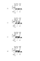
- 4 is a sequence diagram showing each drive signal for driving a unit pixel according to the first embodiment;
- FIG. FIG. 4 is a schematic diagram showing an example of potential transition of each part regarding the operation of the high-sensitivity light receiving element according to the first embodiment;
- FIG. 4 is a schematic diagram showing an example of potential transition of each part regarding the operation of the low-sensitivity light-receiving element according to the first embodiment;
- FIG. 4 is a schematic diagram showing an example of potential transition of each part regarding the operation of the pixel content according to the first embodiment;
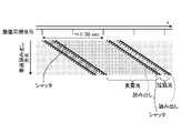
- FIG. 11 is a schematic diagram for explaining operations applicable to the modified example of the first embodiment;
- FIG. 11 is a schematic diagram for explaining another operation applicable to the modified example of the first embodiment;
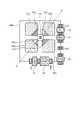
- FIG. 4 is a schematic diagram showing a first example of a planar layout of unit pixels applicable to the first embodiment;
- FIG. 4 is a schematic diagram showing a first example of a cross section of a unit pixel applicable to the first embodiment;
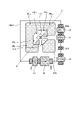
- FIG. 11 is a schematic diagram showing a second example of a planar layout of unit pixels according to another example applicable to the first embodiment;
- FIG. 11 is a schematic diagram showing a third example of a planar layout of unit pixels according to another example applicable to the first embodiment;
- FIG. 11 is a schematic diagram showing a second example of a cross section of a unit pixel according to another example applicable to the first embodiment;
- FIG. 10 is a schematic diagram showing an example of a circuit configuration of a unit pixel according to the second embodiment;
- FIG. 10 is a sequence diagram showing each drive signal for driving a unit pixel according to the second embodiment;
- FIG. 10 is a schematic diagram showing an example of potential transition of each part regarding the operation of the highly sensitive light receiving element according to the second embodiment;
- FIG. 10 is a schematic diagram showing an example of potential transition of each portion of a low-sensitivity light receiving element according to the second embodiment;
- FIG. 10 is a schematic diagram showing an example of potential transition of each part regarding the operation of the pixel content according to the second embodiment; It is a figure explaining the usage example of the imaging device to which the technique of this indication is applied.
- 1 is a block diagram showing an example of a schematic configuration of a vehicle control system;
- FIG. 4 is an explanatory diagram showing an example of installation positions of an outside information detection unit and an imaging unit;
- An imaging device includes a plurality of pixels arranged in a matrix.
- Each of the plurality of pixels includes a first light-receiving element that generates and accumulates photocharges by photoelectric conversion according to the received light, and a second light-receiving element that has a lower sensitivity to light than the first light-receiving element. , and a pixel content for accumulating photocharges spilled from the first and second light receiving elements during the exposure period.
- the overflowing photocharge is accumulated in the pixel content, and the same is also applied to the second light receiving element.
- Photoelectric charges are generated and accumulated by receiving light. Since the second light-receiving element has a lower sensitivity to light than the first light-receiving element, the second light-receiving element accumulates photoelectric charges corresponding to the reception of light with a higher illuminance than the first light-receiving element. is possible.
- the second Photoelectric charges are accumulated in the second light receiving element up to the capacity of the light receiving element.
- the photocharge can be read out from the pixel content in a state where the photocharge is sufficiently accumulated in the pixel content. It is possible to suppress the decrease in
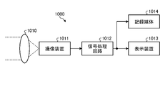
- FIG. 1 is a block diagram showing the configuration of an example of an electronic device to which technology according to embodiments of the present disclosure can be applied.
- the electronic device 1000 includes an optical unit 1010, an imaging device 1011, a signal processing circuit 1012, a display device 1013, and a storage medium 1014.
- an imaging device as an imaging device according to the present disclosure, which will be described later in detail, is applied to the imaging device 1011 .
- the imaging device includes a plurality of pixels that convert incident light into electrical signals by photoelectric conversion, and a drive circuit that drives the plurality of pixels.
- a digital still camera, a digital video camera, a drive recorder, a mobile phone with an imaging function, a smart phone, or the like can be applied.
- the optical unit 1010 includes one or more lenses, a diaphragm mechanism, a focus mechanism, etc., and forms an image of image light (incident light) from a subject on the imaging surface of the imaging device 1011 .
- image light incident light
- a signal processing circuit 1012 performs various kinds of signal processing including image processing on pixel signals output from the imaging device 1011 .
- the image signal that has undergone signal processing can be stored in a non-volatile storage medium 1014 such as a flash memory or a hard disk drive. An image based on the pixel signal can also be output to the display device 1013 .
- FIG. 2 is a block diagram showing a schematic configuration example of a CMOS image sensor applicable to each embodiment.
- a CMOS image sensor is an image sensor manufactured by applying or partially using a CMOS process.
- a CMOS image sensor applicable to each embodiment is configured as a back-illuminated CMOS image sensor.
- an imaging element 10 by a CMOS image sensor applicable to each embodiment has, for example, a stack structure in which a semiconductor chip in which a pixel array section 11 is formed and a semiconductor chip in which a peripheral circuit is formed are stacked.
- Peripheral circuits may include, for example, a vertical drive circuit 12, a column processing circuit 13, a horizontal drive circuit 14, and a system controller 15.
- the imaging device 10 further includes a signal processing section 18 and a data storage section 19 .
- the signal processing unit 18 and the data storage unit 19 may be provided on the same semiconductor chip as the peripheral circuit, or may be provided on a separate semiconductor chip.
- the pixel array section 11 has a configuration in which unit pixels 100 each including a photoelectric conversion element as a light receiving element that generates and accumulates photocharges according to the amount of received light are arranged in a matrix (two-dimensional lattice).
- the row direction refers to the arrangement direction of pixels in a pixel row (that is, the horizontal direction)
- the column direction refers to the arrangement direction of pixels in a pixel column (that is, the vertical direction).
- the unit pixel 100 includes a plurality of light receiving elements. Details of the specific circuit configuration and pixel structure of the unit pixel 100 will be described later.
- the pixel drive lines LD are wired along the row direction for each pixel row and the vertical signal lines VSL are wired along the column direction for each pixel column with respect to the matrix-like pixel array.
- the pixel drive line LD transmits a drive signal for driving when reading a signal from a pixel.
- the pixel drive line LD is shown as one wiring in FIG. 1, the pixel drive line LD actually includes a plurality of signal lines. One end of the pixel drive line LD is connected to the output terminal corresponding to each row of the vertical drive circuit 12 .
- the vertical drive circuit 12 is composed of a shift register, an address decoder, etc., and drives each pixel of the pixel array section 11 simultaneously or in units of rows. That is, the vertical drive circuit 12 constitutes a drive section that controls the operation of each pixel of the pixel array section 11 together with a system control section 15 that controls the vertical drive circuit 12 .
- the vertical drive circuit 12 generally has two scanning systems, a readout scanning system and a discharge scanning system, although the specific configuration thereof is not shown.
- the readout scanning system sequentially selectively scans the unit pixels 100 of the pixel array section 11 row by row in order to read out signals from the unit pixels 100 .
- a row selected for signal readout by the readout scanning system is called an RD row (read row).
- a signal read from the unit pixel 100 is an analog signal.
- the sweep-scanning system performs sweep-scanning ahead of the read-out scanning by the exposure time for the read-out rows to be read-scanned by the read-out scanning system.
- a so-called electronic shutter operation is performed by sweeping out (resetting) unnecessary photocharges with this sweeping scanning system.
- the electronic shutter operation means an operation of discarding the photocharge of the light receiving element and newly starting exposure (starting accumulation of photocharge).
- the rows selected for sweep scanning by the sweep scanning system are called SH rows (shutter rows).
- the signal read out by the readout operation by the readout scanning system corresponds to the amount of light received after the immediately preceding readout operation or the electronic shutter operation.
- the period from the readout timing of the previous readout operation or the sweep timing of the electronic shutter operation to the readout timing of the current readout operation is a photoelectric charge accumulation period (also referred to as an exposure period) in the unit pixel 100 .
- a signal output from each unit pixel 100 in a pixel row selectively scanned by the vertical drive circuit 12 is input to the column processing circuit 13 via each vertical signal line VSL for each pixel column.
- the column processing circuit 13 performs predetermined signal processing on a signal output from each unit pixel 100 of the selected row via the vertical signal line VSL for each pixel column of the pixel array section 11, and performs a predetermined signal processing on the signal output after the signal processing. Temporarily holds the pixel signal.
- the column processing circuit 13 performs at least noise removal processing, such as CDS (Correlated Double Sampling) processing and DDS (Double Data Sampling) processing, as signal processing.
- CDS Correlated Double Sampling
- DDS Double Data Sampling
- the CDS processing removes pixel-specific fixed pattern noise such as reset noise and variations in threshold values of amplification transistors in the unit pixel 100 .
- the column processing circuit 13 also has an AD (analog-digital) conversion function, for example, and converts analog pixel signals read from the photoelectric conversion elements into digital signals and outputs the digital signals.
- AD analog-digital
- the horizontal driving circuit 14 is composed of shift registers, address decoders, etc., and sequentially selects readout circuits (hereinafter referred to as pixel circuits) of the unit pixels 100 corresponding to the pixel columns of the column processing circuit 13 .
- pixel circuits readout circuits
- the system control unit 15 is composed of a timing generator that generates various timing signals. and other drive control.
- the signal processing unit 18 has at least an arithmetic processing function, and performs various signal processing such as arithmetic processing on pixel signals output from the column processing circuit 13 .
- the data storage unit 19 temporarily stores data required for signal processing in the signal processing unit 18 .
- the output image output from the signal processing unit 18 is subjected to predetermined processing in an application processor or the like in an electronic device in which the image sensor 10 is mounted, or is transmitted to an external device via a predetermined network.
- FIG. 3A is a schematic diagram showing an example of a circuit configuration of a unit pixel 100 according to existing technology.
- the unit pixel 100a includes four light receiving elements 20 1 , 20 2 , 20 3 and 20 4 each of which is a photodiode.
- FIG. 3B is a diagram showing an example arrangement of the four light receiving elements 20 1 to 20 4 included in the unit pixel 100a.
- the unit pixel 100a has four light receiving elements 20 1 to 20 4 arranged in an array of 2 rows ⁇ 2 columns, and a color filter is provided for each unit pixel 100a.
- Each unit pixel 100a provided with color filters of R (red), G (green) and B (blue) is arranged according to the Bayer arrangement. Note that the arrangement of the unit pixels 100a is not limited to the Bayer arrangement.
- the unit pixel 100a further includes transfer transistors 21 1 , 21 2 , 21 3 and 21 4 corresponding to the light receiving elements 20 1 , 20 2 , 20 3 and 20 4 respectively, and a reset transistor 30 , a conversion efficiency switching transistor 31 , an amplification transistor 32 , a selection transistor 33 and a storage transistor 34 .
- Each of these transistors is composed of an n-type MOS (Metal Oxide Semiconductor) transistor.
- at least the transfer transistors 21 1 to 21 4 , the conversion efficiency switching transistor 31 and the storage transistor 34 are depletion type MOS transistors.
- Each of the light receiving elements 20 1 to 20 4 has its anode connected to the ground potential, and each cathode connected to the floating diffusion layer FD1 via the transfer transistors 21 1 to 21 4 , respectively.
- a driving signal TG is commonly input to each gate of each of the transfer transistors 21 1 to 21 4 .
- the floating diffusion layer FD1 is further connected to the source of the conversion efficiency switching transistor 31 and the gate of the amplification transistor 32.
- the conversion efficiency switching transistor 31 has a drain connected to the floating diffusion layer FD2 and a gate to which the drive signal FDG is input.
- the conversion efficiency switching transistor 31 is turned on by the driving signal FDG, the floating diffusion layer FD1 and the floating diffusion layer FD2 are coupled, and when the floating diffusion layer FD1 and the floating diffusion layer FD2 are turned off, the floating diffusion layer FD1 and the floating diffusion layer FD2 are connected. split.
- the floating diffusion layer FD2 is further connected to the source of the reset transistor 30 and the source of the storage transistor .
- the reset transistor 30 has a drain connected to the voltage VDD and a gate to which the drive signal RST is input.
- the storage transistor 34 has a drain connected to the floating diffusion layer FD3 and a gate drive signal ECG. When the storage transistor 34 is turned on by the driving signal ECG, the floating diffusion layer FD3 and the floating diffusion layer FD2 are coupled, and when it is turned off, the floating diffusion layer FD3 and the floating diffusion layer FD4 are separated. be.
- One end of the pixel content EC is further connected to the floating diffusion layer FD3. The other end of the pixel content EC is connected to the voltage ECVDD.
- the amplification transistor 32 has a gate connected to FD1, a drain connected to the voltage VDD, and a source connected to the drain of the selection transistor 33, as described above.
- the select transistor 33 has a source connected to the vertical signal line VSL and a gate to which the drive signal SEL is input. Photocharges accumulated in the floating diffusion layer FD1 are converted into voltage when read out from the floating diffusion layer FD1. A pixel signal obtained by converting the photocharge into a voltage is amplified by the amplification transistor 32, and the selection transistor 33 is turned on by the drive signal SEL while the selection transistor 33 is turned on by the drive signal SEL. is output to the vertical signal line VSL through the VSL.
- the driving signal FDG is set to a high state to turn on the conversion efficiency switching transistor 31 to couple the floating diffusion layer FD1 and the floating diffusion layer FD2, thereby reducing the noise level N2 in the low conversion efficiency region.
- the floating diffusion layer FD1 and the floating diffusion layer FD2 are separated by setting the drive signal FDG to a low state and the conversion efficiency switching transistor 31 to be in a non-conducting state, thereby reducing the noise level N1 in the high conversion efficiency region.
- the transfer transistors 21 1 to 21 4 are brought into a conductive state by setting the drive signal TG to a high state, and the photoelectric charges accumulated in the light receiving elements 20 1 to 20 4 are merged and transferred to the floating diffusion layer FD1. Then, the driving signal TG is set to a low state to bring the transfer transistors 21 1 to 21 4 into a non-conducting state, and the signal level S1 in the high conversion efficiency region is read out from the FD1.
- the drive signal FDG is set to a high state to turn on the conversion efficiency switching transistor 31 to couple the floating diffusion layer FD1 and the floating diffusion layer FD2. are turned on to transfer all the photocharges accumulated in each of the light receiving elements 20 1 to 20 4 to the coupled floating diffusion layers FD1 and FD2, and the signal level S2 in the low conversion efficiency region is transferred to the floating diffusion layers FD1 and FD2. Read from FD2.
- the transfer transistors 21 1 to 21 4 , the conversion efficiency switching transistor 31 and the storage transistor 34 are depletion type transistors. Therefore, the photocharges overflowing the light receiving elements 20 1 to 20 4 due to the reception of light of high illuminance pass through the transfer transistors 21 1 to 21 4 , the conversion efficiency switching transistor 31 and the storage transistor 34, and the pixel content is Accumulated in EC.
- the driving signal FDG is set to a high state to turn on the conversion efficiency switching transistor 31 to couple the floating diffusion layer FD1 and the floating diffusion layer FD2.
- Drive signal ECG is set to a high state to bring storage transistor 34 into a conductive state, and floating diffusion layer FD3 is further coupled to coupled floating diffusion layers FD1 and FD2.
- the photocharge accumulated in the pixel content EC is transferred to the combined floating diffusion layers FD1, FD2 and FD3.
- a signal level S4 is read from the coupled floating diffusion layers FD1, FD2 and FD3.
- the driving signal RST is set to a high state to render the reset transistor 30 conductive, thereby resetting the photocharges accumulated in the floating diffusion layers FD1, FD2, and FD3. Then, after driving signal RST is brought to a low state to render reset transistor 30 non-conductive, noise level N4 is read out from coupled floating diffusion layers FD1, FD2 and FD3.
- the noise level N1 is subtracted from the signal level S1 to generate a pixel signal in the high conversion efficiency region.
- the CDS subtracts the noise level N2 from the signal level S2 to generate the pixel signal in the low conversion efficiency region.
- the signal level S4 and the noise level N4 since the signal level S4 is read out first, the pixel signal is generated by subtracting the noise level N4 from the signal level S4 by DDS.
- the noise level N2 When the noise level N2 is subtracted from the signal level S2 by the CDS, the noise level N2 and the signal level S2 are not read out continuously, so a line memory is required to temporarily hold the noise level N2. becomes.
- the voltage ECVDD connected to the other end of the pixel content EC may be a power supply voltage, a ground voltage, or an arbitrary fixed potential.
- FIG. 4 is a graph showing an example of SNR (Signal-Noise Ratio: SN ratio) characteristics with respect to Illuminance in a configuration based on existing technology.
- SNR Signal-Noise Ratio: SN ratio
- the horizontal axis indicates the logarithmic illuminance
- the vertical axis indicates the SNR [dB].
- the range from the low illuminance side to the peak A of the SNR curve 200 shows the SNR characteristics of the light receiving elements 20 1 to 20 4
- the range from the peak A to the high illuminance side shows the SNR characteristics of the pixel content EC. showing.
- a peak A and a dip corresponding to the peak A indicate a joint between the SNR characteristics of the light receiving elements 20 1 to 20 4 and the SNR characteristics of the pixel content EC.
- the illuminance of peak A corresponds to the upper limit of the amount of photocharge that the light receiving elements 20 1 to 20 4 can store. From ⁇ 20 4 photocharges will overflow.
- pixel signals are generated based on photocharges accumulated in the respective light receiving elements 20 1 to 20 4 . Photocharges overflowing from the light receiving elements 20 1 to 20 4 are merged and accumulated in the pixel internal capacity EC on the high illuminance side from the peak A, and the pixel is based on the photocharge accumulated in the pixel internal capacity EC. A signal is generated.
- a peak/dip C indicates a connecting portion between the low conversion efficiency region and the high conversion efficiency region in each of the light receiving elements 20 1 to 20 4 .
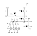
- FIG. 5A is a schematic diagram illustrating an example of a circuit configuration of a unit pixel according to the first embodiment;
- the drive signals TGL, TGS, FDG, ECG, RST and SEL are generated by the vertical drive circuit 12 under the control of the system control section 15 and supplied to the pixel array section 11 row by row.
- a unit pixel 100b has light receiving elements 20L 1 to 20L 3 out of a plurality of light receiving elements 20S, 20L 1 , 20L 2 and 20L 3 in comparison with the unit pixel 100a according to the existing technology described using FIG. 3A.
- the (first light-receiving element) uses transfer transistors 21L 1 , 21L 2 and 21L 3 (first transistors) whose conduction/non-conduction states are controlled by a common drive signal TGL. merge through and transferred to the floating diffusion layer FD1.
- the light-receiving element 20S (second light-receiving element) is connected to the floating diffusion layer FD1 through a transfer transistor 21S (second transistor) whose conduction/non-conduction state is controlled by a drive signal TGS different from the drive signal TGL. transferred to That is, the light receiving elements 20L 1 to 20L 3 and the light receiving element 20S are independently controlled.
- Each of the light receiving elements 20L 1 , 20L 2 and 20L 3 corresponds to a third light receiving element. Further, each of the light receiving elements 20L 1 , 20L 2 and 20L 3 has a light receiving surface size substantially equal to that of the light receiving element 20S. In addition, in the example of FIG. 5A, one light receiving element 20S is provided for three light receiving elements 20L 1 , 20L 2 and 20L 3 , but this is not limited to this example, and the number of light receiving elements 20S should be less than the number of light receiving elements 20L 1 , 20L 2 and 20L 3 .
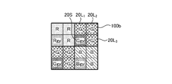
- FIG. 5B is a diagram showing an example of the arrangement of the light receiving element 20S and the light receiving elements 20L 1 to 20L 3 included in the unit pixel 100b according to the first embodiment.
- the unit pixel 100b has the light receiving element 20S and the light receiving elements 20L 1 to 20L 3 arranged in an array of 2 rows ⁇ 2 columns. and B color filters are provided.
- the low-sensitivity light receiving element 20S can be provided with a neutral density filter (ND filter) in addition to the R, G, and B color filters.
- ND filter is an optical filter that is achromatic (has no color information) and has a transmission greater than 0% and less than 100%.
- the filter Ggy indicates a state in which an ND filter is provided for the G color filter.
- filters Rgy and Bgy indicate the state in which ND filters are provided for the R-color and B-color filters, respectively.
- the light-receiving surface of the three light-receiving elements 20L 1 to 20L 3 in which the transferred photocharges are merged and the light-receiving surface of the single light-receiving element 20S correspond to the area ratio. Therefore, the light receiving element 20S becomes less sensitive to light than the light receiving elements 20L 1 to 20L 3 in which the photocharges are merged. That is, the light-receiving element 20S can receive light with a higher illuminance than the set of the light-receiving elements 20L 1 to 20L 3 .
- the decrease in the SNR at the illuminance at which the readout source of the photocharge is switched from each of the light receiving elements 20 1 to 20 4 to the pixel content EC, indicated by symbol “A” in the graph of FIG. can be covered by a pixel signal according to the readout.
- FIG. 5C is a schematic diagram illustrating another example of the circuit configuration of the unit pixel according to the first embodiment; FIG. In the example of FIG. 5C, a connection point connecting the light receiving element 20L 1 and the transfer transistor 21L 1 , a connection point connecting the light receiving element 20L 2 and the transfer transistor 21L 2 , and a connection point connecting the light receiving element 20L 3 and the transfer transistor 21L 3 are connected to each other.
- the photocharges accumulated in the respective light receiving elements 20L 1 to 20L 3 are merged, and the merged photocharges are distributed to the transfer transistors 21L 1 to 21L 3 and transferred to the floating diffusion layer FD1. be done.
- the read source of the photoelectric charges indicated by symbol “ A " in the graph of FIG. It is possible to cover the decrease in SNR in the switching illuminance with the pixel signal according to the readout of the photocharge from the light receiving element 20S.
- the floating diffusion layer FD1 and the floating diffusion layer FD2 are separated by setting the drive signal FDG to a low state and the conversion efficiency switching transistor 31 to be in a non-conducting state, thereby reducing the noise level N1 in the high conversion efficiency region. Read from the floating diffusion layer FD1.
- the transfer transistors 21L 1 to 21L 3 are brought into a conductive state by setting the drive signal TGL to a high state to merge the photocharges accumulated in the light receiving elements 20L 1 to 20L 3 and transfer them to the floating diffusion layer FD1. Then, the drive signal TGL is set to a low state to bring the transfer transistors 21L 1 to 21L 3 into a non-conducting state, and the signal level S1 in the high conversion efficiency region is read out from the FD1.
- the drive signal FDG is set to a high state to turn on the conversion efficiency switching transistor 31 to couple the floating diffusion layer FD1 and the floating diffusion layer FD2. are turned on to transfer all the photocharges accumulated in each of the light receiving elements 20 1 to 20 4 to the coupled floating diffusion layers FD1 and FD2, and the signal level S2 in the low conversion efficiency region is transferred to the floating diffusion layers FD1 and FD2. Read from FD2.
- the driving signal TGS is set to a high state to turn on the transfer transistor 21S, thereby transferring the photoelectric charges accumulated in the light receiving element 20S to the floating diffusion layer FD1, thereby obtaining the signal Level S3 is read from the floating diffusion layer FD1.
- the transfer transistors 21 1 to 21 4 , the conversion efficiency switching transistor 31 and the storage transistor 34 are depletion type transistors. Therefore, the photocharges overflowing the light receiving elements 20 1 to 20 4 due to the reception of light of high illuminance pass through the transfer transistors 21 1 to 21 4 , the conversion efficiency switching transistor 31 and the storage transistor 34, and the pixel content is Accumulated in EC.
- the driving signal FDG is set to a high state to turn on the conversion efficiency switching transistor 31 to couple the floating diffusion layer FD1 and the floating diffusion layer FD2.
- the storage transistor 34 (third transistor) is made conductive by setting the drive signal ECG to a high state, and the floating diffusion layer FD3 is further coupled to the coupled floating diffusion layers FD1 and FD2.
- the photocharge accumulated in the pixel content EC is transferred to the combined floating diffusion layers FD1, FD2 and FD3.
- a signal level S4 is read from the coupled floating diffusion layers FD1, FD2 and FD3.
- the driving signal RST is set to a high state to render the reset transistor 30 conductive, thereby resetting the photocharges accumulated in the floating diffusion layers FD1, FD2, and FD3. Then, after driving signal RST is brought to a low state to render reset transistor 30 non-conductive, noise level N4 is read out from coupled floating diffusion layers FD1, FD2 and FD3.
- the noise level N1 is subtracted from the signal level S1 by the CDS to generate pixel signals from the high conversion efficiency regions of the light receiving elements 20L 1 to 20L 3 .
- the CDS subtracts the noise level N2 from the signal level S2 to generate pixel signals from the low conversion efficiency regions of the light receiving elements 20L 1 to 20L 3 .
- the CDS subtracts the noise level N3 from the signal level S3 to generate a pixel signal by the light receiving element 20S.
- the signal level S4 and the noise level N4 since the signal level S4 is read out first, the pixel signal is generated by subtracting the noise level N4 from the signal level S4 by DDS.
- the noise level N2 When the noise level N2 is subtracted from the signal level S2 by the CDS, the noise level N2 and the signal level S2 are not read out continuously, so a line memory is required to temporarily hold the noise level N2. becomes.
- the voltage ECVDD connected to the other end of the pixel content EC may be a power supply voltage, a ground voltage, or an arbitrary fixed potential.
- FIG. 6 is a graph showing an example of the relationship between illuminance and SN ratio in the configuration according to the first embodiment.
- parts corresponding to those in FIG. 4 described above are denoted by the same reference numerals, and detailed description thereof will be omitted.
- the range from the low illuminance side to the peak A' of the SNR curve 210 shows the SNR characteristics of the light receiving elements 20L 1 to 20L 3
- the range from the peak A' to the peak D shows the SNR characteristics of the light receiving element 20S. (high conversion efficiency region)
- the high illuminance side of the peak D shows the SNR characteristics of the pixel content EC.
- the illuminance of peak A' corresponds to the upper limit of the amount of photocharge that the light receiving elements 20L 1 to 20L 3 can store. Photocharges overflow from 20L 1 to 20L 3 . On the lower illuminance side than this peak A', pixel signals are generated based on photocharges accumulated in the respective light receiving elements 20L 1 to 20L 3 . Photocharges overflowing from the light receiving elements 20L 1 to 20L 3 are merged and accumulated in the pixel content EC on the high illuminance side of the peak A'.
- the peak D which has a higher illuminance than the peak A', corresponds to the upper limit of the photocharge amount that can be accumulated.
- a pixel signal is generated based on the photocharge accumulated in the light receiving element 20S at an illuminance between peak A' and peak D, which is indicated by a range gy in FIG. Further, on the high illuminance side of this peak D, photocharges overflowing from the light receiving element 20S are further accumulated in the pixel content EC. In FIG. 6, on the high illuminance side of peak D, a pixel signal is generated based on the photocharge accumulated in the pixel content EC.
- the pixel content EC is provided in the unit pixel 100b, and the light receiving elements 20L 1 to 20L 3 having high sensitivity to light and the light receiving elements having low sensitivity to light 20S are provided.
- a dip E in FIG. 6 a decrease in SNR at the joint between the SNR characteristics of the light receiving elements 20L 1 to 20L 3 and the SNR characteristic of the light receiving element 20S is suppressed.
- a dip F in FIG. 6 a decrease in SNR is also suppressed at the joint between the SNR characteristic of the light receiving element 20S and the SNR characteristic of the pixel content EC. Therefore, it is possible to suppress deterioration in image quality in intermediate gradations of an image.
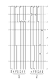
- FIG. 7 is a sequence diagram showing each drive signal for driving the unit pixel 100b according to the first embodiment.
- the top row shows the horizontal synchronizing signal XHS
- the lower row shows the shutter row (SH row)
- the lower row shows each drive signal for the read row (RD row).
- a period from time t 0 to t 8 is one horizontal period.
- the drive signals are drive signals SEL, FDG, RST, ECG, TGL, and TGS from the top in both the SH row and the RD row.
- Each of these drive signals is generated by the vertical drive circuit 12 under the control of the system control section 15 and supplied to each section of the unit pixel 100b.
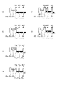
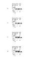
- 8A, 8B, and 8C respectively show the high-sensitivity light-receiving elements 20L 1 to 20L 3 , the low-sensitivity light-receiving element 20S, and the pixel content EC according to the first embodiment.
- black portions of the floating diffusion layers FD1 and FD2 indicate charges present in the initial state.
- the potential at which the light receiving elements 20L 1 to 20L 3 are coupled is indicated as SP1.
- the potential of the light receiving element 20S is indicated as SP2.
- 8A, 8B and 8C, the floating diffusion layers FD1 and FD2 , and the pixel content EC in FIG. shows the photocharge generated by
- FIG. 8A An example of the potential of each part at time t sh is shown in section (a) of FIG. 8A, section (a) of FIG. 8B, and section (a) of FIG. 8C, respectively.
- the transfer transistors 21L 1 to 21L 3 , the conversion efficiency switching transistor 31 and the reset transistor 30 are each turned on, and the charge of SP1 is drained by the power supply voltage VDD.
- the drive signals TGS and TGL are brought to a low state for a short period of time, and the transfer transistors 21S and 21L 1 to 21L 3 are rendered non-conductive. This high/low state transition of the driving signals TGS and TGL is used as a shutter operation, and exposure is started in the light receiving element 20S and the light receiving elements 20L 1 to 20L 3 .
- the driving signal ECG is brought to a high state, the storage transistor 34 is brought into a conductive state, and the pixel content EC is reset.
- Drive signal RST is brought to a low state at time t7 , and reset transistor 30 is rendered non-conductive.
- the driving signals FDG and ECG are brought to a low state, and the conversion efficiency switching transistor 31 and the storage transistor 34 are brought to a non-conducting state.
- operation transitions to row RD.
- the period from time t8 in the SH row until the operation shifts to the RD row is the exposure period.
- FIGS. 8A, 8B and 87C An example of the potential of each part during the exposure period is shown in section (b) of each of FIGS. 8A, 8B and 87C.
- the period from just before time t 8 in row SH in FIG. 7 to time t 0 in row RD is shown.
- SP1 and SP2 accumulate photocharges generated by the light receiving elements 20L 1 to 20L 3 and 20S by light reception due to exposure, respectively.
- charges are generated and accumulated in the floating diffusion layers FD1 and FD2 due to exposure.
- Charges accumulated in the floating diffusion layers FD1 and FD2 become noise for pixel signals.
- photocharges overflowing from, for example, the light receiving elements 20L 1 to 20L 3 are accumulated in the pixel content EC.
- the drive signals SEL and FDG are brought to a high state immediately after time t0 , and the selection transistor 33 and the conversion efficiency switching transistor 31 are brought into a conducting state.
- the high state of drive signal SEL is maintained until just before time t7 .
- the drive signals RST, ECG, TGL, and TGS are in a low state during the period from time t 0 to t 1 , and the reset transistor 30, the storage transistor 34, the transfer transistors 21L 1 to 21L 3 and 21S are in a non-conducting state, respectively. .
- Section (c) of FIG. 8A shows an example of the potential of each part during the period from the drive signals SEL and FDG to the high state immediately after time t 0 to time t 1 .
- the state of SP1 remains unchanged and photocharge storage is maintained.
- Drive signal FDG renders conversion efficiency switching transistor 31 conductive to couple floating diffusion layers FD1 and FD2. Since the drive signal SEL is in a high state, the charges accumulated in the coupled floating diffusion layers FD1 and FD2 are converted into a voltage and applied to the vertical signal line via the selection transistor 33 as the noise level N2 in the low conversion efficiency region. supplied to the VSL.
- the drive signal FDG is brought to a low state, the conversion efficiency switching transistor 31 is brought into a non-conducting state, and the floating diffusion layers FD1 and FD2 are divided.
- Section (d) of FIG. 8A shows an example of the potential of each part during the period from time t 1 to just before the drive signal TGL is set to the high state.
- the state of SP1 remains unchanged and photocharge storage is maintained. Since the drive signal FDG is in the low state and the drive signal SEL is in the high state, the charge accumulated in the floating diffusion layer FD1 is converted into a voltage and applied to the vertical signal line VSL as the noise level N1 through the selection transistor 33. supplied.
- the drive signal TGL is set to a high state, the transfer transistors 21L 1 to 21L 3 are turned on, and the photocharges accumulated in the light receiving elements 20L 1 to 20L 3 due to exposure are transferred. It is transferred to the floating diffusion layer FD1. Since the drive signal SEL is in a high state, the photocharge accumulated in the floating diffusion layer FD1 is converted into a voltage and supplied to the vertical signal line VSL via the selection transistor 33 as the signal level S1 in the high conversion efficiency region. be done.
- Section (e) of FIG. 8A shows an example of the potential of each part during the period from time t2 to time t3. Photoelectric charges transferred from the light receiving elements 20L 1 to 20L 3 are accumulated in the floating diffusion layer FD1 by the conduction of the transfer transistors 21L 1 to 21L 3 .
- the drive signal FDG is brought to a high state, the conversion efficiency switching transistor 31 is turned on, and the floating diffusion layers FD1 and FD2 are coupled. Further, the drive signal TGL is set to the high state for a short period from time t 3 , and the transfer transistors 21L 1 to 21L 3 are turned on. As a result, all photocharges accumulated in the light receiving elements 20L 1 to 20L 3 are transferred to the coupled floating diffusion layers FD1 and FD2. Since the drive signal SEL is in a high state, the photocharges accumulated in the coupled floating diffusion layers FD1 and FD2 are converted into a voltage and applied to the vertical voltage through the selection transistor 33 as the signal level S2 in the low conversion efficiency region. It is supplied to the signal line VSL.
- photocharges accumulated in the coupled floating diffusion layers FD1 and FD2 are all swept out from the floating diffusion layers FD1 and FD2 after a predetermined time, for example, by time t4.
- Section ( f) of FIG. 8A shows an example of the potential of each part from when the drive signal TGL is set to the low state at time t3 to time t4.
- Section (e) shows how photocharges accumulated in SP1 are transferred to the coupled floating diffusion layers FD1 and FD2.
- Section (c) of FIG. 8B shows an example of the potential of each part from time t 4 to just before the drive signal TGS is set to a high state just before time t 5 .
- the photocharge accumulated in SP2 is maintained, and the charge accumulated in the coupled floating diffusion layers FD1 and FD2 is converted into a voltage and supplied as noise level N3 to the vertical signal line VSL via the selection transistor 33. .
- the drive signal TGS is brought to a high state just before time t5 and is brought to a low state at time t5 .
- Section (d) of FIG. 8B shows an example of the potential of each part from time t 5 to time t 6 .
- Photocharges accumulated in the light receiving element 20S are transferred to and accumulated in the coupled floating diffusion layers FD1 and FD2. Since the drive signal SEL is in a high state, the photocharges accumulated in the coupled floating diffusion layers FD1 and FD2 are converted into a voltage and output through the selection transistor 33 as a signal level S3 by the low-sensitivity light receiving element 20S. and supplied to the vertical signal line VSL.
- drive signal ECG Shortly after time t6 , drive signal ECG is brought to a high state and storage transistor 34 is rendered conductive. Further, the drive signal SEL is set to a low state a predetermined time before time t7 , and the selection transistor 33 is turned off. Furthermore, just before time t7 (after the drive signal SEL goes low), the drive signal RST goes high and the reset transistor 30 becomes conductive.
- Section (c) of FIG. 8C shows an example of the potential of each part during the period from the time t6 to time t7 , from when the drive signal ECG is set to a high state to when the drive signal SEL is set to a low state. show.
- the photocharge stored in the pixel content EC is transferred via the storage transistor 34 to the coupled floating diffusion layers FD1 and FD2. Note that the floating diffusion layer FD1 is omitted in section (c) of FIG. 8C and section (d) described later. Since the drive signal SEL is in the high state, the photocharge accumulated in the coupled floating diffusion layers FD1 and FD2 is converted into a voltage and applied to the vertical voltage through the selection transistor 33 as a signal level S4 according to the pixel content EC. It is supplied to the signal line VSL.
- Drive signal RST is brought to a high state just before time t7 and is brought to a low state at time t7 .
- the reset transistor 30 is rendered conductive just before time t7 , and the charges accumulated in the coupled floating diffusion layers FD1 and FD2 are drained by the power supply voltage VDD.
- Section (d) of FIG. 8C shows an example of the potential of each part during the period from time t7 to time t8 in which the drive signal SEL is in the high state.
- the drive signal SEL Since the drive signal SEL is in a high state, the charge accumulated in the pixel content EC and the coupled floating diffusion layers FD1 and FD2 is converted into a voltage, and the noise level N4 due to the pixel content EC is generated by the selection transistor 33. to the vertical signal line VSL.
- a modification of the first embodiment performs exposure (referred to as long-time exposure) and reading according to the sequence described with reference to FIGS. This is an example of performing time exposure).
- drive signals RST, ECG, TGL, and TGS are brought to a low state to render reset transistor 30, storage transistor 34, transfer transistors 21S and 21L 1 -21L 3 non-conductive.
- the drive signal SEL is set to a high state and FDG is set to a high state to couple the floating diffusion layers FD1 and FD2, and the noise level N5 is read out from the coupled floating diffusion layers FD1 and FD2.
- the transfer transistors 21L 1 to 21L 3 are brought into a conductive state by setting the drive signal TGL to a high state, and the photocharges accumulated in the highly sensitive light receiving elements 20L 1 to 20L 3 are transferred to the coupled floating diffusion layers FD1 and FD2. Forward. Then, the drive signal TGL is brought to a low state to render the transfer transistors 21L 1 to 21L 3 non-conductive, and the signal level S5 is read out from the coupled floating diffusion layers FD1 and FD2.
- the noise level N5 is obtained before the signal level S5. Therefore, the process of subtracting the noise level N5 from the signal level S5 can be performed using the CDS.
- the noise level N5 is subtracted from the signal level S5 by the CDS to generate pixel signals from the highly sensitive light receiving elements 20L 1 to 20L 3 .
- a pixel signal obtained by subtracting the noise level N1 from the signal level S1, a pixel signal obtained by subtracting the noise level N2 from the signal level S2, a pixel signal obtained by subtracting the noise level N3 from the signal level S3, and a noise level N5 from the signal level S5. and the subtracted pixel signal are combined to generate a final pixel signal.
- FIG. 9 is a schematic diagram for explaining operations applicable to the modification of the first embodiment.
- the horizontal axis indicates time
- the vertical axis indicates each row in the pixel array section 11 of the image sensor 10 . The reading of each row is performed sequentially from the top row to the bottom row, shown as the vertical readout direction.
- long-time exposure (denoted as long exposure in the figure) and short-time exposure (denoted as short exposure in the figure) are performed according to vertical synchronization signals supplied at intervals of 1/60 [sec].
- a shutter operation is performed for each row by SH rows in response to a vertical synchronization signal, and a readout operation is performed for each row by RD rows in response to the next vertical synchronization signal.
- a shutter operation is performed after a period E of a predetermined length has passed for each row from the vertical synchronizing signal, and a reading operation is performed according to the vertical synchronizing signal following the vertical synchronizing signal. In this manner, long-time exposure and short-time exposure are alternately repeated for each vertical synchronization signal.
- FIG. 10 is a schematic diagram for explaining another operation applicable to the modification of the first embodiment.
- the long exposure is performed for a sufficiently long time, and the short exposure is performed immediately after the long exposure.
- long-time exposure and short-time exposure are repeatedly performed in units of two vertical synchronization signals. An image of one frame is generated every 1/30 [sec] as in the example of FIG.
- an image based on pixel signals obtained by long-time exposure and an image based on pixel signals obtained by short-time exposure executed immediately after the long-time exposure are synthesized to form an image of one frame.
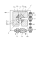
- FIG. 11A is a schematic diagram showing a first example of a planar layout of a unit pixel 100b applicable to the first embodiment. Note that FIG. 11A shows an example of a planar layout corresponding to the circuit of FIG. 5A described above.
- the light receiving element 20S, the light receiving element 20L 1 , the light receiving element 20L 2 , and the light receiving element 20L 3 are arranged in the order of lower right, lower left, upper left, upper right.
- Transfer transistors 21S, 21L 1 , 21L 2 and 21L 3 are arranged at positions where the vertices of the light receiving elements 20S, 20L 1 , 20L 2 and 20L 3 gather.
- a floating diffusion layer FD1 is arranged in contact with each of the transfer transistors 21S, 21L 1 , 21L 2 and 21L 3 .
- the reset transistor 30 and the conversion efficiency switching transistor 31 are arranged on the right side of the unit pixel 100b, and the amplification transistor 32 and the selection transistor 33 are arranged on the lower side. Also, the storage transistor 34 is arranged at a position where the right side and the bottom side of the unit pixel 100b are in contact with each other.
- FIG. 11B is a schematic diagram showing a first example of a cross section of a unit pixel 100b applicable to the first embodiment.
- FIG. 11B shows an example of the A-A' cross section in FIG. 11A.
- FIG. 11B shows a back-illuminated pixel structure, and the lower part of the figure is the light incident surface.
- a wiring layer 51 is provided on the upper surface of the semiconductor layer 50 .
- the semiconductor layer 50 is, for example, a p-type silicon substrate, and the light-receiving elements 20L 1 and 20L 3 are made of an n-type semiconductor formed by ion implantation of high-concentration impurities.
- the p-type semiconductor region functions as an element isolation section that isolates the adjacent light receiving elements 20L 1 and 20L 3 .
- a trench 54 formed from the light incident surface side and embedded with an oxide film or a metal material also constitutes an element isolation portion.
- an oxide film or a metal film provided between adjacent light receiving elements forms an inter-pixel separation section 52 .
- a color filter CF is provided for each light receiving element, and a microlens ML is provided for each light receiving element via a smoothing film 53 .
- a floating diffusion layer FD ⁇ b>1 is provided on a surface of the semiconductor layer 50 in contact with the wiring layer 51 .
- transfer transistors 21L 1 and 21L 3 are provided corresponding to the light receiving elements 20L 1 and 20L 3 , respectively.
- a lower electrode 56 of the pixel content EC is provided on the upper surface of the layer in which the transfer transistors 21L 1 and 21L 3 are provided.
- An upper electrode 58 of the pixel internal volume EC is provided via an insulating film 57 for the lower electrode 56 of the pixel internal volume EC.
- the pixel internal capacity EC is made larger.
- the top electrode 58 of the pixel content EC is connected to the voltage ECVDD.
- FIG. 12A is a schematic diagram showing a second example of a planar layout of a unit pixel 100b' according to another example applicable to the first embodiment.
- FIG. 12A shows an example of a planar layout corresponding to the circuit of FIG. 5C described above.
- the light receiving elements 20L 1 , 20L 2 and 20L 3 are connected, and the transfer transistors 21L 1 , 21L 2 and 21L 3 are also connected. It is configured.
- the arrangement of the reset transistor 30, the conversion efficiency switching transistor 31, the amplification transistor 32, the selection transistor 33, and the storage transistor 34 is the same as that shown in FIG. .
- FIG. 12B is a schematic diagram showing a third example of the planar layout of the unit pixel 100b′ according to another example applicable to the first embodiment. Note that FIG. 12B shows an example of a planar layout corresponding to the circuit of FIG. 5C described above. In the example of FIG. 12B, each light receiving element 20L 1 , light receiving element 20L 2 and light receiving element 20L 3 are joined to the unit pixel 100b′. On the other hand, each transfer transistor 21L 1 , 21L 2 and 21L 3 is configured independently.
- FIG. 12C is a schematic diagram showing a second example of a cross section of a unit pixel 100b′ according to another example applicable to the first embodiment. Note that the cross-sectional view shown in FIG. 12C is common to the planar layouts of FIGS. 12A and 12B, and FIG. 12C shows an example of the AA′ cross section in FIGS. 12A and 12B. As shown in FIG. 12C, the unit pixel 100b′ is configured by joining the light receiving element 20L 1 and the light receiving element 20L 3 between the bottom of the trench 54 and the wiring layer 51 . Other parts are the same as those in FIG. 11B described above, so descriptions thereof are omitted here.
- FIG. 13 is a schematic diagram illustrating an example of a circuit configuration of a unit pixel according to the second embodiment; The following description will focus on the parts that differ from the configuration in FIG. 5A.
- a unit pixel 100c is provided with an OFG transistor 35 (fifth transistor) in addition to the unit pixel 100b in FIG. 5A.
- the OFG transistor 35 is an n-type depletion type MOS transistor.
- the OFG transistor 35 has a drain connected to the floating diffusion layer FD3 and a source connected to a connection point connecting the cathode of the low-sensitivity light receiving element 20S and the source of the transfer transistor 21S.
- the drive signal OFG is always kept low in both SH row and RD row operations.
- the cathodes of the light receiving elements 20L 1 to 20L 3 are connected to each other, and the photoelectric charges of the light receiving elements 20L 1 to 20L 3 are merged and transferred. This connection between the cathodes of the light receiving elements 20L 1 to 20L 3 can be omitted.
- FIG. 14 is a sequence diagram showing each drive signal for driving the unit pixel 100c according to the second embodiment. Since the meaning of each part in FIG. 14 is the same as that of each part in FIG. 7 described above, description thereof will be omitted here.
- the sequence shown in FIG. 14 differs from the above-described sequence of FIG. 7 in that the drive signal RST goes high for a short time at time t 10 immediately after time t 0 in the operation of the RD row. Further, since the OFG transistor 35 is of a depletion type, even if the drive signal OFG input to the gate is in a low state and is in a non-conducting state, charges can pass between the drain and the source.
- FIGS. 15A, 15B, and 15C respectively show the high-sensitivity light-receiving elements 20L 1 to 20L 3 , the low-sensitivity light-receiving element 20S, and the pixel content EC according to the second embodiment.
- the meaning of each part in FIGS. 15A to 15C is the same as that of each part in FIGS. 15A to 15C described above, so description thereof will be omitted here.
- the driving signal ECG is brought to a high state, the storage transistor 34 is brought into a conductive state, and the pixel content EC is reset.
- FIG. 15A An example of the potential of each part at time t sh is shown in section (a) of FIG. 15A, section (a) of FIG. 15B, and section (a) of FIG. 15C, respectively.
- the transfer transistors 21L 1 to 21L 3 , the conversion efficiency switching transistor 31 and the reset transistor 30 are each rendered conductive, and the charge of SP1 is drained by the power supply voltage VDD.
- the drive signals TGS and TGL are brought to a low state for a short period of time, and the transfer transistors 21S and 21L 1 to 21L 3 are rendered non-conductive.
- This high/low state transition of the driving signals TGS and TGL is used as a shutter operation, and exposure is started in the light receiving element 20S and the light receiving elements 20L 1 to 20L 3 .
- the period from the start of exposure until the operation shifts to the RD row is the exposure period.
- Drive signal RST is brought to a low state at time t7 , and reset transistor 30 is rendered non-conductive.
- the driving signals FDG and ECG are brought to a low state, and the conversion efficiency switching transistor 31 and the storage transistor 34 are brought to a non-conducting state.
- FIG. 15A, 15B and 15C An example of the potential of each part during the exposure period is shown in section (b) of each of FIGS. 15A, 15B and 15C. Here, it shows the period from when the drive signals TGL and TGS, which are in the high state at time t sh in FIG.
- SP1 and SP2 store photocharges generated by the light receiving elements 20L 1 to 20L 3 and 20S by light reception due to exposure, respectively.
- Photocharges overflowing from the light receiving elements 20L 1 to 20L 3 are transferred to the floating diffusion layer FD3 and the pixel content EC via the OFG transistor 35, as shown in section (b) of FIG. 15C.
- Photocharges overflowing from the light receiving elements 20L 1 to 20L 3 are also transferred to the floating diffusion layer FD1 via the transfer transistors 21L 1 to 21L 3 as shown in section (b) of FIG. 15A.
- drive signals SEL, FDG and RST are brought to a high state at time t 10 immediately after time t 0 , and selection transistor 33, conversion efficiency switching transistor 31 and reset transistor 30 are rendered conductive.
- the drive signal RST is brought to a low state for a short period of time, and the reset transistor 30 becomes non-conductive.
- the high state of drive signal SEL is maintained until just before time t7 .
- the drive signals ECG, TGL and TGS are kept low during the period from time t 0 to t 1 , and the storage transistor 34 and the transfer transistors 21L 1 to 21L 3 and 21S are rendered non-conductive.
- the drive signal FDG is brought to a low state, the conversion efficiency switching transistor 31 is brought into a non-conducting state, and the floating diffusion layers FD1 and FD2 are divided.
- Section (d) of FIG. 15A shows an example of the potential of each part during the period from time t 1 to just before the driving signal TGL is set to the high state.
- the state of SP1 remains unchanged and photocharge storage is maintained. Since the drive signal FDG is in the low state and the drive signal SEL is in the high state, the electric charge existing in the floating diffusion layer FD1 is converted into a voltage, and the noise level N1 is applied to the vertical signal line VSL through the selection transistor 33. supplied.
- the drive signal RST is brought to a high state, the reset transistor 30 is brought into a conductive state, and the charges are drained from the floating diffusion layers FD1 and FD2. It becomes a low level with respect to the noise level N1 in the form.
- the drive signal TGL is set to a high state
- the transfer transistors 21L 1 to 21L 3 are turned on, and the photocharges accumulated in the light receiving elements 20L 1 to 20L 3 due to exposure. is transferred to the floating diffusion layer FD1. Since the drive signal SEL is in a high state, the photocharge accumulated in the floating diffusion layer FD1 is converted into a voltage and supplied to the vertical signal line VSL via the selection transistor 33 as the signal level S1 in the high conversion efficiency region. be done.
- Section (e) of FIG. 15A shows an example of the potential of each part during the period from time t 2 to time t 3 .
- Photoelectric charges transferred from the light receiving elements 20L 1 to 20L 3 are accumulated in the floating diffusion layer FD1 by the conduction of the transfer transistors 21L 1 to 21L 3 .
- the drive signal FDG is brought to a high state, the conversion efficiency switching transistor 31 is turned on, and the floating diffusion layers FD1 and FD2 are coupled. Further, the drive signal TGL is set to the high state for a short period from time t 3 , and the transfer transistors 21L 1 to 21L 3 are turned on. As a result, all photocharges accumulated in the light receiving elements 20L 1 to 20L 3 are transferred to the coupled floating diffusion layers FD1 and FD2. Since the drive signal SEL is in a high state, the photocharges accumulated in the coupled floating diffusion layers FD1 and FD2 are converted into a voltage and applied to the vertical voltage through the selection transistor 33 as the signal level S2 in the low conversion efficiency region. It is supplied to the signal line VSL.
- photocharges accumulated in the coupled floating diffusion layers FD1 and FD2 are all swept out from the floating diffusion layers FD1 and FD2 after a predetermined time, for example, by time t4.
- Section ( f) of FIG. 15A shows an example of the potential of each part from when the drive signal TGL is set to the low state at time t3 to time t4.
- Section (e) shows how photocharges accumulated in SP1 are transferred to the coupled floating diffusion layers FD1 and FD2.
- Section ( c) of FIG. 15B shows an example of the potential of each part from the time t4 to just before the drive signal TGS is set to the high state just before the time t5.
- the photocharge accumulated in SP2 is maintained, and the charge accumulated in the coupled floating diffusion layers FD1 and FD2 is converted into a voltage and supplied as noise level N3 to the vertical signal line VSL via the selection transistor 33.
- the drive signal RST is brought to a high state
- the reset transistor 30 is brought into a conductive state, and the charges are drained from the floating diffusion layers FD1 and FD2. It becomes a low level with respect to the noise level N3 in the form.
- the drive signal TGS is brought to a high state just before time t5 and is brought to a low state at time t5 .
- Section (d) of FIG. 15B shows an example of the potential of each part from time t 5 to time t 6 .
- Photocharges accumulated in the light receiving element 20S are transferred to and accumulated in the coupled floating diffusion layers FD1 and FD2. Since the drive signal SEL is in a high state, the photocharges accumulated in the coupled floating diffusion layers FD1 and FD2 are converted into a voltage and output through the selection transistor 33 as a signal level S3 by the low-sensitivity light receiving element 20S. and supplied to the vertical signal line VSL.
- drive signal ECG Shortly after time t6 , drive signal ECG is brought to a high state and storage transistor 34 is rendered conductive. Further, the drive signal SEL is set to a low state a predetermined time before time t7 , and the selection transistor 33 is turned off. Furthermore, just before time t7 (after the drive signal SEL goes low), the drive signal RST goes high and the reset transistor 30 becomes conductive.
- Section (c) of FIG. 15C shows an example of the potential of each part during the period from the time t6 to time t7 , from when the drive signal ECG is set to a high state to when the drive signal SEL is set to a low state. show. Photocharges accumulated in floating diffusion layer FD3 and pixel content EC are transferred via storage transistor 34 to coupled floating diffusion layers FD1 and FD2. Note that the floating diffusion layer FD1 is omitted in section (c) of FIG. 15C and section (d) described later.
- the drive signal SEL Since the drive signal SEL is in a high state, the photoelectric charges accumulated in the coupled floating diffusion layers FD1 and FD2 are converted into a voltage, and the signal level S4 by the floating diffusion layer FD3 and the pixel internal capacitance EC is generated by the selection transistor. 33 to the vertical signal line VSL.
- the signal level S4 here is higher than the signal level S4 in the first embodiment.
- Drive signal RST is brought to a high state just before time t7 and is brought to a low state at time t7 .
- the reset transistor 30 is rendered conductive just before time t7 , and the charges accumulated in the coupled floating diffusion layers FD1 and FD2 are drained by the power supply voltage VDD.
- Section (d) of FIG. 15C shows an example of the potential of each part during the period when the drive signal SEL is in the high state within the period from time t7 to time t8.
- the drive signal SEL Since the drive signal SEL is in a high state, the charges accumulated in the floating diffusion layer FD3 and the pixel content EC, and the coupled floating diffusion layers FD1 and FD2 are converted into voltages, and the noise due to the pixel content EC is converted into a voltage. It is supplied to the vertical signal line VSL through the selection transistor 33 as the level N4.
- the pixel content EC is provided in the unit pixel 100b or the unit pixel 100c, and the light receiving element 20L 1 having high sensitivity to light is provided. 20L 3 and a light receiving element 20S having a low sensitivity to light are provided.
- a dip E in FIG. 6 a decrease in SNR at the joint between the SNR characteristics of the light receiving elements 20L 1 to 20L 3 and the SNR characteristic of the light receiving element 20S is suppressed.
- a path is provided for directly transferring the photocharges overflowing from the low-sensitivity light receiving element 20S to the pixel internal capacity EC, so control is easier than in the first embodiment. is.
- each embodiment of the present disclosure is suitable for use in an image sensor for in-vehicle use.
- a phenomenon called "LED flicker” in which a blinking subject such as an LED (Light Emitting Diode) light source cannot be imaged depending on the timing of the blinking, has attracted attention. .
- This LED flicker is a defect caused by the existing image sensor, which has a narrow dynamic range and needs to adjust the exposure time for each subject.
- the exposure time is long for subjects with low illuminance, and the exposure time is short for subjects with high illuminance. This makes it possible to handle various subjects even with a narrow dynamic range.
- a method that combines a method of using a sensitivity ratio due to space division, as disclosed in US Patent Application Publication No. 2018/0241955, and a method of directly increasing the amount of charge handled by providing a capacitance in the pixel. is suitable for expanding the dynamic range while coping with LED flicker.
- the number of manufacturing steps increases.
- the pixel content EC is provided in the unit pixel 100b or the unit pixel 100c, and the light receiving elements 20L 1 to 20L 3 having high sensitivity to light are provided. and a light receiving element 20S having low sensitivity to light.
- the decrease in SNR is suppressed respectively. Therefore, it is possible to suppress deterioration of image quality in intermediate gradations of an image, realize a wider dynamic range, and cope with LED flicker.
- the number of light receiving elements provided in a unit pixel is not limited to four, and may be three, or may be five or more.
- the number of low-sensitivity light-receiving elements among the plurality of light-receiving elements provided in the unit pixel is not limited to one, and may be two or more. That is, it is possible to provide two light receiving portions each including a plurality of light receiving elements in a unit pixel, one of the two light receiving portions to have low sensitivity and the other light receiving portion to have high sensitivity.
- the sizes of the plurality of light receiving elements included in the unit pixel are substantially the same, but this is not limited to this example. That is, the sizes of the plurality of light receiving elements included in the unit pixel may be different.
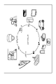
- FIG. 16 is a diagram showing a usage example using the image sensor according to the above-described first embodiment, its modifications, and the second embodiment.
- the imaging device 10 described above can be used in various cases for sensing light such as visible light, infrared light, ultraviolet light, and X-rays, as follows.
- a device that takes pictures for viewing such as a digital camera or a mobile device with a camera function.
- a device used for transportation such as a ranging sensor that measures the distance of a vehicle.
- a device used in home appliances such as TVs, refrigerators, air conditioners, etc., to photograph a user's gesture and operate the device according to the gesture.
- Medical and health care devices such as endoscopes and devices that perform angiography by receiving infrared light.
- ⁇ Devices used for security such as monitoring cameras for crime prevention and cameras for person authentication.
- ⁇ Equipment used for beauty care such as a skin measuring instrument for photographing the skin and a microscope for photographing the scalp.
- ⁇ Equipment used for sports such as action cameras and wearable cameras for sports.
- - Equipment for agricultural use such as cameras for monitoring the condition of fields and crops.
- FIG. 17 is a block diagram showing a schematic configuration example of a vehicle control system, which is an example of a mobile control system to which the technology according to the present disclosure can be applied.
- a vehicle control system 12000 includes a plurality of electronic control units connected via a communication network 12001.
- vehicle control system 12000 includes drive system control unit 12010 , body system control unit 12020 , vehicle exterior information detection unit 12030 , vehicle interior information detection unit 12040 , and integrated control unit 12050 .
- integrated control unit 12050 As the functional configuration of the integrated control unit 12050, a microcomputer 12051, an audio/image output section 12052, and an in-vehicle network I/F (interface) 12053 are illustrated.
- the drive system control unit 12010 controls the operation of devices related to the drive system of the vehicle according to various programs.
- the driving system control unit 12010 includes a driving force generator for generating driving force of the vehicle such as an internal combustion engine or a driving motor, a driving force transmission mechanism for transmitting the driving force to the wheels, and a steering angle of the vehicle. It functions as a control device such as a steering mechanism to adjust and a brake device to generate braking force of the vehicle.
- the body system control unit 12020 controls the operation of various devices equipped on the vehicle body according to various programs.
- the body system control unit 12020 functions as a keyless entry system, a smart key system, a power window device, or a control device for various lamps such as headlamps, back lamps, brake lamps, winkers or fog lamps.
- the body system control unit 12020 can receive radio waves transmitted from a portable device that substitutes for a key or signals from various switches.
- the body system control unit 12020 receives the input of these radio waves or signals and controls the door lock device, power window device, lamps, etc. of the vehicle.
- the vehicle exterior information detection unit 12030 detects information outside the vehicle in which the vehicle control system 12000 is installed.
- the vehicle exterior information detection unit 12030 is connected with an imaging section 12031 .
- the vehicle exterior information detection unit 12030 causes the imaging unit 12031 to capture an image of the exterior of the vehicle, and receives the captured image.
- the vehicle exterior information detection unit 12030 may perform object detection processing or distance detection processing such as people, vehicles, obstacles, signs, or characters on the road surface based on the received image.
- the vehicle exterior information detection unit 12030 for example, performs image processing on the received image, and performs object detection processing and distance detection processing based on the result of the image processing.
- the imaging unit 12031 is an optical sensor that receives light and outputs an electrical signal according to the amount of received light.
- the imaging unit 12031 can output the electric signal as an image, and can also output it as distance measurement information.
- the light received by the imaging unit 12031 may be visible light or non-visible light such as infrared rays.
- the in-vehicle information detection unit 12040 detects in-vehicle information.
- the in-vehicle information detection unit 12040 is connected to, for example, a driver state detection section 12041 that detects the state of the driver.
- the driver state detection unit 12041 includes, for example, a camera that captures an image of the driver, and the in-vehicle information detection unit 12040 detects the degree of fatigue or concentration of the driver based on the detection information input from the driver state detection unit 12041. It may be calculated, or it may be determined whether the driver is dozing off.
- the microcomputer 12051 calculates control target values for the driving force generator, the steering mechanism, or the braking device based on the information inside and outside the vehicle acquired by the vehicle exterior information detection unit 12030 or the vehicle interior information detection unit 12040, and controls the drive system control unit.
- a control command can be output to 12010 .
- the microcomputer 12051 realizes the functions of ADAS (Advanced Driver Assistance System) including collision avoidance or shock mitigation, follow-up driving based on inter-vehicle distance, vehicle speed maintenance driving, vehicle collision warning, vehicle lane departure warning, etc. Cooperative control can be performed for the purpose of ADAS (Advanced Driver Assistance System) including collision avoidance or shock mitigation, follow-up driving based on inter-vehicle distance, vehicle speed maintenance driving, vehicle collision warning, vehicle lane departure warning, etc. Cooperative control can be performed for the purpose of ADAS (Advanced Driver Assistance System) including collision avoidance or shock mitigation, follow-up driving based on inter-vehicle distance, vehicle speed maintenance driving, vehicle collision warning, vehicle
- the microcomputer 12051 controls the driving force generator, the steering mechanism, the braking device, etc. based on the information about the vehicle surroundings acquired by the vehicle exterior information detection unit 12030 or the vehicle interior information detection unit 12040, so that the driver's Cooperative control can be performed for the purpose of autonomous driving, etc., in which vehicles autonomously travel without depending on operation.
- the microcomputer 12051 can output a control command to the body system control unit 12020 based on the information outside the vehicle acquired by the information detection unit 12030 outside the vehicle.
- the microcomputer 12051 controls the headlamps according to the position of the preceding vehicle or the oncoming vehicle detected by the vehicle exterior information detection unit 12030, and performs cooperative control aimed at anti-glare such as switching from high beam to low beam. It can be carried out.
- the audio/image output unit 12052 transmits at least one of audio and/or image output signals to an output device capable of visually or audibly notifying the passengers of the vehicle or the outside of the vehicle.
- an audio speaker 12061, a display unit 12062 and an instrument panel 12063 are illustrated as output devices.
- the display unit 12062 may include at least one of an on-board display and a head-up display, for example.
- FIG. 18 is a diagram showing an example of the installation position of the imaging unit 12031.
- vehicle 12100 has imaging units 12101 , 12102 , 12103 , 12104 and 12105 as imaging unit 12031 .
- the imaging units 12101, 12102, 12103, 12104, and 12105 are provided at positions such as the front nose, side mirrors, rear bumper, back door, and windshield of the vehicle 12100, for example.
- An image pickup unit 12101 provided in the front nose and an image pickup unit 12105 provided above the windshield in the passenger compartment mainly acquire images in front of the vehicle 12100 .
- Imaging units 12102 and 12103 provided in the side mirrors mainly acquire side images of the vehicle 12100 .
- An imaging unit 12104 provided in the rear bumper or back door mainly acquires an image behind the vehicle 12100 .
- the front images acquired by the imaging units 12101 and 12105 are mainly used for detecting preceding vehicles, pedestrians, obstacles, traffic lights, traffic signs, lanes, and the like.
- FIG. 18 shows an example of the imaging range of the imaging units 12101-12104.
- the imaging range 12111 indicates the imaging range of the imaging unit 12101 provided in the front nose
- the imaging ranges 12112 and 12113 indicate the imaging ranges of the imaging units 12102 and 12103 provided in the side mirrors, respectively
- the imaging range 12114 The imaging range of an imaging unit 12104 provided on the rear bumper or back door is shown. For example, by superimposing the image data captured by the imaging units 12101 to 12104, a bird's-eye view image of the vehicle 12100 viewed from above can be obtained.
- At least one of the imaging units 12101 to 12104 may have a function of acquiring distance information.
- at least one of the imaging units 12101 to 12104 may be a stereo camera composed of a plurality of imaging elements, or may be an imaging element having pixels for phase difference detection.
- the microcomputer 12051 determines the distance to each three-dimensional object within the imaging ranges 12111 to 12114 and changes in this distance over time (relative velocity with respect to the vehicle 12100). , it is possible to extract, as the preceding vehicle, the closest three-dimensional object on the course of the vehicle 12100, which runs at a predetermined speed (for example, 0 km/h or more) in substantially the same direction as the vehicle 12100. can. Furthermore, the microcomputer 12051 can set the inter-vehicle distance to be secured in advance in front of the preceding vehicle, and perform automatic brake control (including following stop control) and automatic acceleration control (including following start control). In this way, cooperative control can be performed for the purpose of automatic driving in which the vehicle runs autonomously without relying on the operation of the driver.
- automatic brake control including following stop control
- automatic acceleration control including following start control
- the microcomputer 12051 based on the distance information obtained from the imaging units 12101 to 12104, converts three-dimensional object data to other three-dimensional objects such as two-wheeled vehicles, ordinary vehicles, large vehicles, pedestrians, and utility poles. It can be classified and extracted and used for automatic avoidance of obstacles. For example, the microcomputer 12051 distinguishes obstacles around the vehicle 12100 into those that are visible to the driver of the vehicle 12100 and those that are difficult to see. Then, the microcomputer 12051 judges the collision risk indicating the degree of danger of collision with each obstacle, and when the collision risk is equal to or higher than the set value and there is a possibility of collision, an audio speaker 12061 and a display unit 12062 are displayed. By outputting an alarm to the driver via the drive system control unit 12010 and performing forced deceleration and avoidance steering via the drive system control unit 12010, driving support for collision avoidance can be performed.
- the microcomputer 12051 based on the distance information obtained from the imaging units 12101 to 12104, converts three-dimensional object data to other three-
- At least one of the imaging units 12101 to 12104 may be an infrared camera that detects infrared rays.
- the microcomputer 12051 can recognize a pedestrian by determining whether or not the pedestrian is present in the captured images of the imaging units 12101 to 12104 .
- recognition of a pedestrian is performed by, for example, a procedure for extracting feature points in images captured by the imaging units 12101 to 12104 as infrared cameras, and performing pattern matching processing on a series of feature points indicating the outline of an object to determine whether or not the pedestrian is a pedestrian.
- the audio image output unit 12052 outputs a rectangular outline for emphasis to the recognized pedestrian. is superimposed on the display unit 12062 . Also, the audio/image output unit 12052 may control the display unit 12062 to display an icon or the like indicating a pedestrian at a desired position.
- the technology according to the present disclosure can be applied to, for example, the imaging unit 12031 among the configurations described above.
- the imaging device 1 using the imaging element 10 to which the above-described first embodiment and its modifications and the second embodiment can be applied can be applied to the imaging unit 12031.
- the exposure time in the imaging element 10 can be increased, LED flicker can be dealt with, and noise in the intermediate gradation of the image is suppressed, resulting in a higher image quality.
- a captured image with high image quality can be obtained. This allows the driver to drive more safely.
- the present technology can also take the following configuration.
- a first light-receiving element and a second light-receiving element for generating and accumulating photoelectric charges by photoelectric conversion in accordance with the received light; a pixel content amount for accumulating the photoelectric charges overflowing from the first light receiving element and the second light receiving element during an exposure period; pixels containing with The second light receiving element has a lower sensitivity to the light than the first light receiving element, image sensor.
- the pixels are The first light receiving element includes one or more third light receiving elements having substantially the same size as the second light receiving element, The imaging device according to (1) above.
- the pixels are readout of photocharges accumulated in the first light receiving element and readout of photoelectrons accumulated in the second light receiving element are independently controlled; The imaging device according to (2) above.
- the pixels are the first light receiving element including two or more of the third light receiving elements; a number of the second light receiving elements less than the number of the third light receiving elements; including, The imaging device according to (3) above.
- the second light receiving element is provided with a neutral density filter on the light receiving surface. The imaging device according to any one of (2) to (4).
- the pixels are a floating diffusion layer that converts the photocharge into voltage; a first transistor that transfers photocharges accumulated in the first light receiving element to the floating diffusion layer; a second transistor that transfers the photocharge accumulated in the second light receiving element to the floating diffusion layer; a third transistor coupling and dividing the floating diffusion layer and the pixel content; a fourth transistor dividing and coupling the floating diffusion layer; further comprising The imaging device according to any one of (2) to (5) above. (7) The pixels are further comprising a fifth transistor that transfers the photocharge accumulated in the second light receiving element to the pixel content; The imaging device according to (6) above. (8) wherein the third transistor and the fourth transistor are depletion mode transistors; The imaging device according to (6) or (7) above.
- the pixels are One said first transistor is provided for said first light receiving element, The imaging device according to any one of (6) to (8) above. (10) The pixels are The first transistor is provided in a one-to-one correspondence with the third light receiving element, The imaging device according to any one of (6) to (9).
- a first light-receiving element and a second light-receiving element for generating and accumulating photoelectric charges by photoelectric conversion in accordance with the received light; a pixel content amount for accumulating the photoelectric charges overflowing from the first light receiving element and the second light receiving element during an exposure period; a pixel containing a driving unit for driving the pixels; a recording unit for recording pixel signals output from the pixels based on the photocharges accumulated in the first light receiving element and the second light receiving element; with The second light receiving element has a lower sensitivity to the light than the first light receiving element, Imaging device.
Landscapes
- Engineering & Computer Science (AREA)
- Multimedia (AREA)
- Signal Processing (AREA)
- Physics & Mathematics (AREA)
- Spectroscopy & Molecular Physics (AREA)
- Solid State Image Pick-Up Elements (AREA)
- Transforming Light Signals Into Electric Signals (AREA)
Abstract
Description
1.本開示の概要
2.本開示に適用可能な技術
2-1.電子機器
2-2.CMOSイメージセンサの概略構成
3.既存技術について
4.本開示の第1の実施形態
4-1.第1の実施形態に係る構成例
4-2.第1の実施形態に係る単位画素の駆動方法
4-3.第1の実施形態の変形例
4-4.第1の実施形態に適用可能な単位画素の平面レイアウトおよび積層構造例
5.本開示の第2の実施形態
5-1.第2の実施形態に係る構成例
5-2.第2の実施形態に係る画素の駆動方法
6.効果
7.本開示の第3の実施形態
7-1.本開示の技術の適用例
7-2.移動体への適用例
本開示に係る撮像素子は、行列状の配列で配置される複数の画素を備える。複数の画素のそれぞれは、それぞれ受光した光に応じた光電変換により光電荷を生成して蓄積する第1の受光素子および第1の受光素子より光に対する感度が低くされた第2の受光素子と、露光期間中に第1の受光素子および第2の受光素子から溢れた光電荷を蓄積する画素内容量と、を含む。
次に、本開示の各実施形態に適用可能な技術について、概略的に説明する。
先ず、本開示の各実施形態に係る技術を適用可能な電子機器について説明する。図1は、本開示の各実施形態に係る技術を適用可能な電子機器の一例の構成を示すブロック図である。
次に、本開示に係る撮像素子としてのCMOS(Complementary Metal-Oxide-Semiconductor)型の固体撮像素子の概略的な構成について説明する。なお、以下では、CMOS型の固体撮像素子を、CMOSイメージセンサと略称して説明を行う。図2は、各実施形態に適用可能なCMOSイメージセンサの概略構成例を示すブロック図である。ここで、CMOSイメージセンサとは、CMOSプロセスを応用して、または、部分的に使用して作成されたイメージセンサである。例えば、各実施形態に適用可能なCMOSイメージセンサは、裏面照射型のCMOSイメージセンサで構成されている。
次に、本開示に係る各実施形態の説明に先んじて、理解を容易とするために、本開示に関連する既存技術について説明する。
次に、本開示の第1の実施形態について説明する。
図5Aは、第1の実施形態に係る単位画素の回路構成の例を示す模式図である。なお、図5Aにおいて、各駆動信号TGL、TGS、FDG、ECG、RSTおよびSELは、システム制御部15の制御に従い、垂直駆動回路12により生成され、行毎に画素アレイ部11に供給される。
図5Cは、第1の実施形態に係る単位画素の回路構成の別の例を示す模式図である。図5Cの例は、受光素子20L1と転送トランジスタ21L1とを接続する接続点と、受光素子20L2と転送トランジスタ21L2とを接続する接続点と、受光素子20L3と転送トランジスタ21L3とを接続する接続点と、が互いに接続された例である。
次に、第1の実施形態に係る単位画素100bの駆動方法について説明する。先ず、図5Aの構成における動作について、概略的に説明する。一定の露光時間の後、駆動信号FDGをハイ状態として変換効率切替トランジスタ31(第4のトランジスタ)を導通状態にして浮遊拡散層FD1と浮遊拡散層FD2とを結合し、低変換効率領域におけるノイズレベルN2を結合された浮遊拡散層FD1およびFD2から読み出す。次に、駆動信号FDGをロー(Low)状態として変換効率切替トランジスタ31を非導通状態にして結合された浮遊拡散層FD1と浮遊拡散層FD2とを分割し、高変換効率領域におけるノイズレベルN1を浮遊拡散層FD1から読み出す。
先ず、SH行における動作について説明する。SH行において、駆動信号SELが常時ロー状態とされ、選択トランジスタ33が非導通状態とされる。駆動信号FDGが時点t3でハイ状態とされ変換効率切替トランジスタ31が導通状態となる。駆動信号RSTが時点t6でハイ状態とされ、リセットトランジスタ30が導通状態となる。すなわち、時点t6では、浮遊拡散層FD1およびFD2が結合されると共に、電源電圧VDDに接続され、リセットされる。
次に、RD行における動作について説明する。なお、上述したように、RD行における時点t0~t8は、SH行における時点t0~t8と一致していなくて良い。
次に、第1の実施形態の変形例について説明する。第1の実施形態の変形例は、図7および図8A~図8Cを用いて説明したシーケンスよる露光(長時間露光と呼ぶ)および読み出しを行った後、当該露光より短い露光時間による露光(短時間露光と呼ぶ)を行う例である。
次に、第1の実施形態に適用可能な単位画素100bの平面レイアウトおよび積層構造の例について説明する。図11Aは、第1の実施形態に適用可能な単位画素100bの平面レイアウトの第1の例を示す模式図である。なお、図11Aは、上述した図5Aの回路に対応する平面レイアウトの例を示している。
次に、本開示の第2の実施形態について説明する。第2の実施形態は、図5Aを用いて説明した構成に対して、低感度の受光素子20Sで生成された光電荷を、高感度の受光素子20L1~21L3で生成された光電荷とマージせずに、画素内容量ECに直接的に転送可能な経路を設けた例である。
図13は、第2の実施形態に係る単位画素の回路構成の例を示す模式図である。以下、図5Aの構成と異なる部分に注目して説明を行う。図13において、単位画素100cは、図5Aの単位画素100bに対してOFGトランジスタ35(第5のトランジスタ)が追加して設けられる。OFGトランジスタ35は、n型のデプレッション型MOSトランジスタである。OFGトランジスタ35は、ドレインが浮遊拡散層FD3に接続され、ソースが低感度の受光素子20Sのカソードと転送トランジスタ21Sのソースとを接続する接続点に接続される。駆動信号OFGは、SH行およびRD行の何れの動作においても、常時ロー状態とされる。
図14は、第2の実施形態に係る単位画素100cを駆動するための各駆動信号を示すシーケンス図である。図14における各部の意味は、上述した図7の各部と同様であるので、ここでの説明を省略する。
先ず、SH行における動作について説明する。SH行において、時点t6の直後の時点tshにおいて、駆動信号TGLおよびTGSがハイ状態とされる。これにより、転送トランジスタ21Sおよび21L1~21L3が導通状態となり、受光素子20Sおよび20L1~20L3がリセットされる。
次に、RD行における動作について説明する。RD行において、時点t0の直後の時点t10で駆動信号SEL、FDGおよびRSTがハイ状態とされ、選択トランジスタ33、変換効率切替トランジスタ31およびリセットトランジスタ30が導通状態となる。駆動信号RSTは、短時間でロー状態とされ、リセットトランジスタ30が非導通状態となる。
次に、本開示の各実施形態による効果について説明する。上述した第1の実施形態およびその変形例、ならびに、第2の実施形態では、単位画素100bまたは単位画素100c内に、画素内容量ECを設けると共に、光に対して高感度の受光素子20L1~20L3と、光に対して低感度の受光素子20Sと、を設ける。これにより、図6にディップEで示されるように、受光素子20L1~20L3のSNR特性と、受光素子20SのSNR特性との継部におけるSNRの低下が抑制される。また、図6にディップFで示されるように、受光素子20SのSNR特性と画素内容量ECのSNR特性との継部においても、SNRの低下が抑制される。したがって、画像の中間階調における画質劣化を抑制することができ、より大きなダイナミックレンジを実現できる。
(7-1.本開示の技術の適用例)
次に、第3の実施形態として、本開示に係る、第1の実施形態およびその変形例、ならびに、第2の実施形態に係る撮像素子の適用例について説明する。図16は、上述の第1の実施形態およびその各変形例、ならびに、第2の実施形態に係る撮像素子を使用する使用例を示す図である。
・自動停止等の安全運転や、運転者の状態の認識等のために、自動車の前方や後方、周囲、車内等を撮影する車載用センサ、走行車両や道路を監視する監視カメラ、車両間等の測距を行う測距センサ等の、交通の用に供される装置。
・ユーザのジェスチャを撮影して、そのジェスチャに従った機器操作を行うために、TVや、冷蔵庫、エアーコンディショナ等の家電に供される装置。
・内視鏡や、赤外光の受光による血管撮影を行う装置等の、医療やヘルスケアの用に供される装置。
・防犯用途の監視カメラや、人物認証用途のカメラ等の、セキュリティの用に供される装置。
・肌を撮影する肌測定器や、頭皮を撮影するマイクロスコープ等の、美容の用に供される装置。
・スポーツ用途等向けのアクションカメラやウェアラブルカメラ等の、スポーツの用に供される装置。
・畑や作物の状態を監視するためのカメラ等の、農業の用に供される装置。
次に、本開示に係る技術のさらなる適用例について説明する。本開示に係る技術は、さらに、自動車、電気自動車、ハイブリッド電気自動車、自動二輪車、自転車、パーソナルモビリティ、飛行機、ドローン、船舶、ロボットといった各種の移動体に搭載される装置に対して適用されてもよい。
(1)
それぞれ受光した光に応じて光電変換により光電荷を生成して蓄積する第1の受光素子および第2の受光素子と、
露光期間中に前記第1の受光素子および前記第2の受光素子から溢れた前記光電荷を蓄積する画素内容量と、
を含む画素、
を備え、
前記第2の受光素子は、前記第1の受光素子より前記光に対する感度が低い、
撮像素子。
(2)
前記画素は、
前記第1の受光素子は前記第2の受光素子とサイズが略等しい第3の受光素子を1以上含む、
前記(1)に記載の撮像素子。
(3)
前記画素は、
前記第1の受光素子に蓄積された光電荷の読み出しと、前記第2の受光素子に蓄積された光電子の読み出しと、が独立して制御される、
前記(2)に記載の撮像素子。
(4)
前記画素は、
前記第3の受光素子を2以上含む前記第1の受光素子と、
前記第3の受光素子より少ない数の前記第2の受光素子と、
を含む、
前記(3)に記載の撮像素子。
(5)
前記第2の受光素子は、受光面に減光フィルタが設けられる、
前記(2)乃至(4)の何れかに記載の撮像素子。
(6)
前記画素は、
光電荷を電圧に変換する浮遊拡散層と、
前記第1の受光素子に蓄積された光電荷を前記浮遊拡散層に転送する第1のトランジスタと、
前記第2の受光素子に蓄積された前記光電荷を前記浮遊拡散層に転送する第2のトランジスタと、
前記浮遊拡散層と前記画素内容量とを結合および分割する第3のトランジスタと、
前記浮遊拡散層を分割および結合する第4のトランジスタと、
をさらに含む、
前記(2)乃至(5)の何れかに記載の撮像素子。
(7)
前記画素は、
前記第2の受光素子に蓄積された光電荷を前記画素内容量に転送する第5のトランジスタをさらに含む、
前記(6)に記載の撮像素子。
(8)
前記第3のトランジスタおよび前記第4のトランジスタは、デプレッション型トランジスタである、
前記(6)または(7)に記載の撮像素子。
(9)
前記画素は、
前記第1の受光素子に対して1つの前記第1のトランジスタが設けられる、
前記(6)乃至(8)の何れかに記載の撮像素子。
(10)
前記画素は、
前記第3の受光素子に対して1対1で前記第1のトランジスタが設けられる、
前記(6)乃至(9)の何れかに記載の撮像素子。
(11)
それぞれ受光した光に応じて光電変換により光電荷を生成して蓄積する第1の受光素子および第2の受光素子と、
露光期間中に前記第1の受光素子および前記第2の受光素子から溢れた前記光電荷を蓄積する画素内容量と、
を含む画素と、
前記画素を駆動する駆動部と、
前記第1の受光素子および前記第2の受光素子に蓄積された光電荷に基づき前記画素から出力される画素信号を記録する記録部と、
を備え、
前記第2の受光素子は、前記第1の受光素子より前記光に対する感度が低い、
撮像装置。
11 画素アレイ部
12 垂直駆動回路
201,202,203,204,20S,20L1,20L2,20L3 受光素子
211,212,213,214,21S,21L1,21L2,21L3 転送トランジスタ
30 リセットトランジスタ
31 変換効率切替トランジスタ
32 増幅トランジスタ
33 選択トランジスタ
34 蓄積トランジスタ
35 OFGトランジスタ
100,100a,100b,100c 単位画素
200,210 SNR曲線
Claims (11)
- それぞれ受光した光に応じて光電変換により光電荷を生成して蓄積する第1の受光素子および第2の受光素子と、
露光期間中に前記第1の受光素子および前記第2の受光素子から溢れた前記光電荷を蓄積する画素内容量と、
を含む画素、
を備え、
前記第2の受光素子は、前記第1の受光素子より前記光に対する感度が低い、
撮像素子。 - 前記画素は、
前記第1の受光素子は前記第2の受光素子とサイズが略等しい第3の受光素子を1以上含む、
請求項1に記載の撮像素子。 - 前記画素は、
前記第1の受光素子に蓄積された光電荷の読み出しと、前記第2の受光素子に蓄積された光電子の読み出しと、が独立して制御される、
請求項2に記載の撮像素子。 - 前記画素は、
前記第3の受光素子を2以上含む前記第1の受光素子と、
前記第3の受光素子より少ない数の前記第2の受光素子と、
を含む、
請求項3に記載の撮像素子。 - 前記第2の受光素子は、受光面に減光フィルタが設けられる、
請求項1に記載の撮像素子。 - 前記画素は、
光電荷を電圧に変換する浮遊拡散層と、
前記第1の受光素子に蓄積された光電荷を前記浮遊拡散層に転送する第1のトランジスタと、
前記第2の受光素子に蓄積された前記光電荷を前記浮遊拡散層に転送する第2のトランジスタと、
前記浮遊拡散層のポテンシャルと前記画素内容量のポテンシャルとを結合および分割する第3のトランジスタと、
前記浮遊拡散層を分割および結合する第4のトランジスタと、
をさらに含む、
請求項2に記載の撮像素子。 - 前記画素は、
前記第2の受光素子に蓄積された光電荷を前記画素内容量に転送する第5のトランジスタをさらに含む、
請求項6に記載の撮像素子。 - 前記第3のトランジスタおよび前記第4のトランジスタは、デプレッション型トランジスタである、
請求項6に記載の撮像素子。 - 前記画素は、
前記第1の受光素子に対して1つの前記第1のトランジスタが設けられる、
請求項6に記載の撮像素子。 - 前記画素は、
前記第3の受光素子に対して1対1で前記第1のトランジスタが設けられる、
請求項6に記載の撮像素子。 - それぞれ受光した光に応じて光電変換により光電荷を生成して蓄積する第1の受光素子および第2の受光素子と、
露光期間中に前記第1の受光素子および前記第2の受光素子から溢れた前記光電荷を蓄積する画素内容量と、
を含む画素と、
前記画素を駆動する駆動部と、
前記第1の受光素子および前記第2の受光素子に蓄積された光電荷に基づき前記画素から出力される画素信号を記録する記録部と、
を備え、
前記第2の受光素子は、前記第1の受光素子より前記光に対する感度が低い、
撮像装置。
Priority Applications (3)
| Application Number | Priority Date | Filing Date | Title |
|---|---|---|---|
| JP2023508742A JPWO2022201898A1 (ja) | 2021-03-25 | 2022-02-04 | |
| US18/550,720 US12556841B2 (en) | 2021-03-25 | 2022-02-04 | Imaging sensor and imaging device |
| CN202280013708.3A CN116830595A (zh) | 2021-03-25 | 2022-02-04 | 成像元件和成像装置 |
Applications Claiming Priority (2)
| Application Number | Priority Date | Filing Date | Title |
|---|---|---|---|
| JP2021052123 | 2021-03-25 | ||
| JP2021-052123 | 2021-03-25 |
Publications (1)
| Publication Number | Publication Date |
|---|---|
| WO2022201898A1 true WO2022201898A1 (ja) | 2022-09-29 |
Family
ID=83396866
Family Applications (1)
| Application Number | Title | Priority Date | Filing Date |
|---|---|---|---|
| PCT/JP2022/004399 Ceased WO2022201898A1 (ja) | 2021-03-25 | 2022-02-04 | 撮像素子および撮像装置 |
Country Status (4)
| Country | Link |
|---|---|
| US (1) | US12556841B2 (ja) |
| JP (1) | JPWO2022201898A1 (ja) |
| CN (1) | CN116830595A (ja) |
| WO (1) | WO2022201898A1 (ja) |
Citations (2)
| Publication number | Priority date | Publication date | Assignee | Title |
|---|---|---|---|---|
| WO2018221261A1 (ja) * | 2017-06-02 | 2018-12-06 | ソニーセミコンダクタソリューションズ株式会社 | 固体撮像装置、及び電子機器 |
| JP2020021987A (ja) * | 2018-07-24 | 2020-02-06 | ソニーセミコンダクタソリューションズ株式会社 | 撮像装置、電子機器 |
Family Cites Families (6)
| Publication number | Priority date | Publication date | Assignee | Title |
|---|---|---|---|---|
| JP4317115B2 (ja) | 2004-04-12 | 2009-08-19 | 国立大学法人東北大学 | 固体撮像装置、光センサおよび固体撮像装置の動作方法 |
| JP5274166B2 (ja) * | 2008-09-10 | 2013-08-28 | キヤノン株式会社 | 光電変換装置及び撮像システム |
| JPWO2017085848A1 (ja) * | 2015-11-19 | 2018-09-06 | オリンパス株式会社 | 固体撮像装置および撮像装置 |
| US11330203B2 (en) * | 2018-07-24 | 2022-05-10 | Sony Semiconductor Solutions Corporation | Imaging device and electronic device |
| KR102709670B1 (ko) * | 2019-08-08 | 2024-09-26 | 에스케이하이닉스 주식회사 | 이미지 센서 |
| KR102823755B1 (ko) * | 2020-08-13 | 2025-06-23 | 에스케이하이닉스 주식회사 | 이미지 센싱 장치 |
-
2022
- 2022-02-04 CN CN202280013708.3A patent/CN116830595A/zh active Pending
- 2022-02-04 US US18/550,720 patent/US12556841B2/en active Active
- 2022-02-04 WO PCT/JP2022/004399 patent/WO2022201898A1/ja not_active Ceased
- 2022-02-04 JP JP2023508742A patent/JPWO2022201898A1/ja active Pending
Patent Citations (2)
| Publication number | Priority date | Publication date | Assignee | Title |
|---|---|---|---|---|
| WO2018221261A1 (ja) * | 2017-06-02 | 2018-12-06 | ソニーセミコンダクタソリューションズ株式会社 | 固体撮像装置、及び電子機器 |
| JP2020021987A (ja) * | 2018-07-24 | 2020-02-06 | ソニーセミコンダクタソリューションズ株式会社 | 撮像装置、電子機器 |
Also Published As
| Publication number | Publication date |
|---|---|
| US12556841B2 (en) | 2026-02-17 |
| JPWO2022201898A1 (ja) | 2022-09-29 |
| US20240155267A1 (en) | 2024-05-09 |
| CN116830595A (zh) | 2023-09-29 |
Similar Documents
| Publication | Publication Date | Title |
|---|---|---|
| KR102560795B1 (ko) | 촬상 장치, 및 전자 기기 | |
| US11336860B2 (en) | Solid-state image capturing device, method of driving solid-state image capturing device, and electronic apparatus | |
| JP7391041B2 (ja) | 固体撮像装置及び電子機器 | |
| US11438533B2 (en) | Solid-state imaging device, method of driving the same, and electronic apparatus | |
| JP2019080305A (ja) | 固体撮像素子、固体撮像素子の駆動方法および電子機器 | |
| US12490529B2 (en) | Solid-state imaging device and electronic apparatus having a storage capacitor with a thin insulating film | |
| CN111863844B (zh) | 成像装置和电子设备 | |
| US20250203232A1 (en) | Solid-state imaging device and electronic device | |
| US20250006751A1 (en) | Imaging device and electronic apparatus | |
| US11438534B2 (en) | Solid-state imaging device and electronic apparatus | |
| WO2020183809A1 (ja) | 固体撮像装置、電子機器、および、固体撮像装置の制御方法 | |
| WO2022244328A1 (ja) | 固体撮像装置および電子機器 | |
| WO2019078110A1 (ja) | 固体撮像素子、固体撮像素子の駆動方法および電子機器 | |
| CN114008783B (zh) | 摄像装置 | |
| WO2022201802A1 (ja) | 固体撮像装置および電子機器 | |
| WO2022201898A1 (ja) | 撮像素子および撮像装置 | |
| US20250063254A1 (en) | Imaging element and electronic apparatus | |
| JP2020115516A (ja) | 撮像装置 | |
| TW202431859A (zh) | 固態攝像裝置 | |
| WO2026094419A1 (ja) | 撮像装置 | |
| TW202329677A (zh) | 攝像裝置 | |
| WO2026004392A1 (ja) | 固体撮像素子 |
Legal Events
| Date | Code | Title | Description |
|---|---|---|---|
| 121 | Ep: the epo has been informed by wipo that ep was designated in this application |
Ref document number: 22774699 Country of ref document: EP Kind code of ref document: A1 |
|
| WWE | Wipo information: entry into national phase |
Ref document number: 202280013708.3 Country of ref document: CN |
|
| WWE | Wipo information: entry into national phase |
Ref document number: 2023508742 Country of ref document: JP |
|
| WWE | Wipo information: entry into national phase |
Ref document number: 18550720 Country of ref document: US |
|
| NENP | Non-entry into the national phase |
Ref country code: DE |
|
| 122 | Ep: pct application non-entry in european phase |
Ref document number: 22774699 Country of ref document: EP Kind code of ref document: A1 |
|
| WWG | Wipo information: grant in national office |
Ref document number: 18550720 Country of ref document: US |