WO2022201835A1 - 撮像素子及び撮像装置 - Google Patents
撮像素子及び撮像装置 Download PDFInfo
- Publication number
- WO2022201835A1 WO2022201835A1 PCT/JP2022/002785 JP2022002785W WO2022201835A1 WO 2022201835 A1 WO2022201835 A1 WO 2022201835A1 JP 2022002785 W JP2022002785 W JP 2022002785W WO 2022201835 A1 WO2022201835 A1 WO 2022201835A1
- Authority
- WO
- WIPO (PCT)
- Prior art keywords
- pixel
- photoelectric conversion
- semiconductor substrate
- imaging device
- charges
- Prior art date
- Legal status (The legal status is an assumption and is not a legal conclusion. Google has not performed a legal analysis and makes no representation as to the accuracy of the status listed.)
- Ceased
Links
Images









Classifications
-
- H—ELECTRICITY
- H04—ELECTRIC COMMUNICATION TECHNIQUE
- H04N—PICTORIAL COMMUNICATION, e.g. TELEVISION
- H04N25/00—Circuitry of solid-state image sensors [SSIS]; Control thereof
- H04N25/70—SSIS architectures; Circuits associated therewith
- H04N25/76—Addressed sensors, e.g. MOS or CMOS sensors
- H04N25/77—Pixel circuitry, e.g. memories, A/D converters, pixel amplifiers, shared circuits or shared components
- H04N25/771—Pixel circuitry, e.g. memories, A/D converters, pixel amplifiers, shared circuits or shared components comprising storage means other than floating diffusion
-
- H—ELECTRICITY
- H04—ELECTRIC COMMUNICATION TECHNIQUE
- H04N—PICTORIAL COMMUNICATION, e.g. TELEVISION
- H04N25/00—Circuitry of solid-state image sensors [SSIS]; Control thereof
- H04N25/10—Circuitry of solid-state image sensors [SSIS]; Control thereof for transforming different wavelengths into image signals
- H04N25/11—Arrangement of colour filter arrays [CFA]; Filter mosaics
- H04N25/13—Arrangement of colour filter arrays [CFA]; Filter mosaics characterised by the spectral characteristics of the filter elements
- H04N25/134—Arrangement of colour filter arrays [CFA]; Filter mosaics characterised by the spectral characteristics of the filter elements based on three different wavelength filter elements
-
- H—ELECTRICITY
- H04—ELECTRIC COMMUNICATION TECHNIQUE
- H04N—PICTORIAL COMMUNICATION, e.g. TELEVISION
- H04N25/00—Circuitry of solid-state image sensors [SSIS]; Control thereof
- H04N25/40—Extracting pixel data from image sensors by controlling scanning circuits, e.g. by modifying the number of pixels sampled or to be sampled
- H04N25/46—Extracting pixel data from image sensors by controlling scanning circuits, e.g. by modifying the number of pixels sampled or to be sampled by combining or binning pixels
-
- H—ELECTRICITY
- H04—ELECTRIC COMMUNICATION TECHNIQUE
- H04N—PICTORIAL COMMUNICATION, e.g. TELEVISION
- H04N25/00—Circuitry of solid-state image sensors [SSIS]; Control thereof
- H04N25/50—Control of the SSIS exposure
- H04N25/57—Control of the dynamic range
-
- H—ELECTRICITY
- H04—ELECTRIC COMMUNICATION TECHNIQUE
- H04N—PICTORIAL COMMUNICATION, e.g. TELEVISION
- H04N25/00—Circuitry of solid-state image sensors [SSIS]; Control thereof
- H04N25/60—Noise processing, e.g. detecting, correcting, reducing or removing noise
- H04N25/62—Detection or reduction of noise due to excess charges produced by the exposure, e.g. smear, blooming, ghost image, crosstalk or leakage between pixels
- H04N25/621—Detection or reduction of noise due to excess charges produced by the exposure, e.g. smear, blooming, ghost image, crosstalk or leakage between pixels for the control of blooming
-
- H—ELECTRICITY
- H04—ELECTRIC COMMUNICATION TECHNIQUE
- H04N—PICTORIAL COMMUNICATION, e.g. TELEVISION
- H04N25/00—Circuitry of solid-state image sensors [SSIS]; Control thereof
- H04N25/70—SSIS architectures; Circuits associated therewith
- H04N25/703—SSIS architectures incorporating pixels for producing signals other than image signals
- H04N25/704—Pixels specially adapted for focusing, e.g. phase difference pixel sets
-
- H—ELECTRICITY
- H04—ELECTRIC COMMUNICATION TECHNIQUE
- H04N—PICTORIAL COMMUNICATION, e.g. TELEVISION
- H04N25/00—Circuitry of solid-state image sensors [SSIS]; Control thereof
- H04N25/70—SSIS architectures; Circuits associated therewith
- H04N25/79—Arrangements of circuitry being divided between different or multiple substrates, chips or circuit boards, e.g. stacked image sensors
-
- H—ELECTRICITY
- H10—SEMICONDUCTOR DEVICES; ELECTRIC SOLID-STATE DEVICES NOT OTHERWISE PROVIDED FOR
- H10F—INORGANIC SEMICONDUCTOR DEVICES SENSITIVE TO INFRARED RADIATION, LIGHT, ELECTROMAGNETIC RADIATION OF SHORTER WAVELENGTH OR CORPUSCULAR RADIATION
- H10F39/00—Integrated devices, or assemblies of multiple devices, comprising at least one element covered by group H10F30/00, e.g. radiation detectors comprising photodiode arrays
- H10F39/011—Manufacture or treatment of image sensors covered by group H10F39/12
- H10F39/014—Manufacture or treatment of image sensors covered by group H10F39/12 of CMOS image sensors
-
- H—ELECTRICITY
- H10—SEMICONDUCTOR DEVICES; ELECTRIC SOLID-STATE DEVICES NOT OTHERWISE PROVIDED FOR
- H10F—INORGANIC SEMICONDUCTOR DEVICES SENSITIVE TO INFRARED RADIATION, LIGHT, ELECTROMAGNETIC RADIATION OF SHORTER WAVELENGTH OR CORPUSCULAR RADIATION
- H10F39/00—Integrated devices, or assemblies of multiple devices, comprising at least one element covered by group H10F30/00, e.g. radiation detectors comprising photodiode arrays
- H10F39/10—Integrated devices
- H10F39/12—Image sensors
- H10F39/18—Complementary metal-oxide-semiconductor [CMOS] image sensors; Photodiode array image sensors
- H10F39/186—Complementary metal-oxide-semiconductor [CMOS] image sensors; Photodiode array image sensors having arrangements for blooming suppression
- H10F39/1865—Overflow drain structures
-
- H—ELECTRICITY
- H10—SEMICONDUCTOR DEVICES; ELECTRIC SOLID-STATE DEVICES NOT OTHERWISE PROVIDED FOR
- H10F—INORGANIC SEMICONDUCTOR DEVICES SENSITIVE TO INFRARED RADIATION, LIGHT, ELECTROMAGNETIC RADIATION OF SHORTER WAVELENGTH OR CORPUSCULAR RADIATION
- H10F39/00—Integrated devices, or assemblies of multiple devices, comprising at least one element covered by group H10F30/00, e.g. radiation detectors comprising photodiode arrays
- H10F39/80—Constructional details of image sensors
- H10F39/802—Geometry or disposition of elements in pixels, e.g. address-lines or gate electrodes
-
- H—ELECTRICITY
- H10—SEMICONDUCTOR DEVICES; ELECTRIC SOLID-STATE DEVICES NOT OTHERWISE PROVIDED FOR
- H10F—INORGANIC SEMICONDUCTOR DEVICES SENSITIVE TO INFRARED RADIATION, LIGHT, ELECTROMAGNETIC RADIATION OF SHORTER WAVELENGTH OR CORPUSCULAR RADIATION
- H10F39/00—Integrated devices, or assemblies of multiple devices, comprising at least one element covered by group H10F30/00, e.g. radiation detectors comprising photodiode arrays
- H10F39/80—Constructional details of image sensors
- H10F39/803—Pixels having integrated switching, control, storage or amplification elements
- H10F39/8037—Pixels having integrated switching, control, storage or amplification elements the integrated elements comprising a transistor
-
- H—ELECTRICITY
- H10—SEMICONDUCTOR DEVICES; ELECTRIC SOLID-STATE DEVICES NOT OTHERWISE PROVIDED FOR
- H10F—INORGANIC SEMICONDUCTOR DEVICES SENSITIVE TO INFRARED RADIATION, LIGHT, ELECTROMAGNETIC RADIATION OF SHORTER WAVELENGTH OR CORPUSCULAR RADIATION
- H10F39/00—Integrated devices, or assemblies of multiple devices, comprising at least one element covered by group H10F30/00, e.g. radiation detectors comprising photodiode arrays
- H10F39/80—Constructional details of image sensors
- H10F39/807—Pixel isolation structures
-
- H—ELECTRICITY
- H10—SEMICONDUCTOR DEVICES; ELECTRIC SOLID-STATE DEVICES NOT OTHERWISE PROVIDED FOR
- H10F—INORGANIC SEMICONDUCTOR DEVICES SENSITIVE TO INFRARED RADIATION, LIGHT, ELECTROMAGNETIC RADIATION OF SHORTER WAVELENGTH OR CORPUSCULAR RADIATION
- H10F39/00—Integrated devices, or assemblies of multiple devices, comprising at least one element covered by group H10F30/00, e.g. radiation detectors comprising photodiode arrays
- H10F39/80—Constructional details of image sensors
- H10F39/811—Interconnections
-
- H—ELECTRICITY
- H10—SEMICONDUCTOR DEVICES; ELECTRIC SOLID-STATE DEVICES NOT OTHERWISE PROVIDED FOR
- H10F—INORGANIC SEMICONDUCTOR DEVICES SENSITIVE TO INFRARED RADIATION, LIGHT, ELECTROMAGNETIC RADIATION OF SHORTER WAVELENGTH OR CORPUSCULAR RADIATION
- H10F39/00—Integrated devices, or assemblies of multiple devices, comprising at least one element covered by group H10F30/00, e.g. radiation detectors comprising photodiode arrays
- H10F39/80—Constructional details of image sensors
- H10F39/813—Electronic components shared by multiple pixels, e.g. one amplifier shared by two pixels
Definitions
- the present disclosure relates to imaging elements and imaging devices.
- An imaging device in which pixels with two photoelectric conversion units are arranged in a two-dimensional matrix.
- This imaging device can pupil-divide incident light from a subject and generate a phase difference signal for detecting an image plane phase difference and an image signal based on the incident light from the subject.
- a phase difference signal two image signals based on charges respectively generated by the photoelectric conversion of the two photoelectric conversion units are output as the phase difference signal.
- an image signal the charges generated by the photoelectric conversion of the two photoelectric conversion units are summed in the pixel, and the image signal generated based on the summed charges is output.
- the two photoelectric conversion units can be separated, for example, by a semiconductor region having a relatively high impurity concentration. Also, a semiconductor region having a relatively high impurity concentration is arranged between the pixels, so that the pixels can be separated from each other.
- the conventional technology described above has a problem that the saturation charge amount of the photoelectric conversion unit when generating the phase difference signal is reduced. Since the potential barrier of the semiconductor region between the two photoelectric conversion units is lowered, the saturated charge amount of each photoelectric conversion unit is lowered. There is a problem that the phase difference detectable range is narrowed when detecting the phase difference signal, and the convenience is lowered.
- the present disclosure proposes an imaging device and an imaging device that prevent the saturation charge amount of the photoelectric conversion unit from decreasing when generating the phase difference signal.
- the present disclosure has been made to solve the above-described problems, and its aspect is to provide a plurality of photoelectric conversion units that are formed on a semiconductor substrate and perform photoelectric conversion of incident light from an object to generate charges.
- a pixel an intra-pixel separation section arranged in the pixel for separating the plurality of photoelectric conversion sections, and an arrangement in the intra-pixel separation section for mutually transferring charges overflowing between the plurality of photoelectric conversion sections.
- an overflow path an overflow gate arranged in the pixel to adjust the potential of the overflow path, a pixel separating section arranged at the boundary of the pixel, a charge holding section holding the generated charge, and the plurality of a plurality of charge transfer units arranged for each of the photoelectric conversion units and transferring the generated charges to the charge holding unit to hold them; and an image signal generation unit for producing image signals based on the held charges image sensor.
- FIG. 2 is a diagram showing a configuration example of a pixel according to an embodiment of the present disclosure
- FIG. 3 is a diagram showing a configuration example of a pixel according to the first embodiment of the present disclosure
- FIG. 2 is a cross-sectional view showing a configuration example of a pixel according to the first embodiment of the present disclosure
- FIG. 2 is a cross-sectional view showing a configuration example of a pixel according to the first embodiment of the present disclosure
- FIG. 4 is a diagram illustrating an example of generation of an image signal and a phase difference signal according to an embodiment of the present disclosure
- FIG. 4 is a diagram illustrating the effect of an overflow gate according to an embodiment of the present disclosure
- FIG. FIG. 4 is a diagram illustrating the effect of an overflow gate according to an embodiment of the present disclosure
- FIG. FIG. 4 is a diagram illustrating the effect of an overflow gate according to an embodiment of the present disclosure
- FIG. FIG. 4 is a diagram showing an example of a method for manufacturing an imaging device according to the first embodiment of the present disclosure
- FIG. FIG. 4 is a diagram showing an example of a method for manufacturing an imaging device according to the first embodiment of the present disclosure
- FIG. FIG. 4 is a diagram showing an example of a method for manufacturing an imaging device according to the first embodiment of the present disclosure
- FIG. FIG. 4 is a diagram showing an example of a method for manufacturing an imaging device according to the first embodiment of the present disclosure
- FIG. FIG. 4 is a diagram showing an example of a method for manufacturing an imaging device according to the first embodiment of the present disclosure
- FIG. 4 is a diagram showing an example of a method for manufacturing an imaging device according to the first embodiment of the present disclosure
- FIG. FIG. 4 is a diagram showing an example of gate voltage measurement of an overflow gate according to the first embodiment of the present disclosure
- FIG. 7 is a diagram showing a configuration example of a pixel according to the second embodiment of the present disclosure
- FIG. 7 is a cross-sectional view showing a configuration example of a pixel according to the second embodiment of the present disclosure
- FIG. 7 is a cross-sectional view showing a configuration example of a pixel according to the second embodiment of the present disclosure
- FIG. 10 is a diagram illustrating an example of a method for manufacturing an imaging device according to the second embodiment of the present disclosure
- FIG. 10 is a diagram illustrating an example of a method for manufacturing an imaging device according to the second embodiment of the present disclosure
- FIG. 10 is a diagram illustrating an example of a method for manufacturing an imaging device according to the second embodiment of the present disclosure
- FIG. 10 is a diagram illustrating a configuration example of a pixel according to a third embodiment of the present disclosure
- FIG. FIG. 7 is a cross-sectional view showing a configuration example of a pixel according to a third embodiment of the present disclosure
- FIG. 7 is a cross-sectional view showing a configuration example of a pixel according to a third embodiment of the present disclosure
- FIG. 10 is a diagram showing an example of a method for manufacturing an imaging device according to the third embodiment of the present disclosure
- FIG. 10 is a diagram showing an example of a method for manufacturing an imaging device according to the third embodiment of the present disclosure
- FIG. 10 is a diagram showing an example of a method for manufacturing an imaging device according to the third embodiment of the present disclosure
- FIG. 10 is a diagram showing an example of a method for manufacturing an imaging device according to the third embodiment of the present disclosure
- FIG. 10 is
- FIG. 10 is a diagram showing an example of a method for manufacturing an imaging device according to the third embodiment of the present disclosure
- FIG. 10 is a diagram showing an example of a method for manufacturing an imaging device according to the third embodiment of the present disclosure
- FIG. 11 is a diagram showing a configuration example of a pixel according to a fourth embodiment of the present disclosure
- FIG. 11 is a cross-sectional view showing a configuration example of a pixel according to a fourth embodiment of the present disclosure
- FIG. 11 is a cross-sectional view showing a configuration example of a pixel according to a fourth embodiment of the present disclosure
- FIG. 11 is a diagram showing another configuration example of a pixel according to the fourth embodiment of the present disclosure
- FIG. 11 is a cross-sectional view showing another configuration example of a pixel according to the fourth embodiment of the present disclosure;
- FIG. 11 is a cross-sectional view showing another configuration example of a pixel according to the fourth embodiment of the present disclosure;
- FIG. 11 is a diagram illustrating a configuration example of a pixel according to a fifth embodiment of the present disclosure;
- FIG. FIG. 11 is a diagram illustrating a configuration example of a pixel according to a sixth embodiment of the present disclosure;
- FIG. FIG. 11 is a cross-sectional view showing a configuration example of a pixel according to a sixth embodiment of the present disclosure;
- FIG. 11 is a cross-sectional view showing a configuration example of a pixel according to a sixth embodiment of the present disclosure;
- FIG. 11 is a cross-sectional view showing a configuration example of a pixel according to a sixth embodiment of the present disclosure;
- FIG. 11 is a cross-sectional view showing a configuration example of a pixel according
- FIG. 12 is a diagram showing an example of a method for manufacturing an imaging device according to the sixth embodiment of the present disclosure
- FIG. 12 is a diagram showing an example of a method for manufacturing an imaging device according to the sixth embodiment of the present disclosure
- FIG. 12 is a diagram showing an example of a method for manufacturing an imaging device according to the sixth embodiment of the present disclosure
- FIG. 12 is a diagram showing an example of a method for manufacturing an imaging device according to the sixth embodiment of the present disclosure
- FIG. 12 is a diagram showing an example of a method for manufacturing an imaging device according to the sixth embodiment of the present disclosure
- FIG. 13 is a diagram illustrating a configuration example of a pixel according to a seventh embodiment of the present disclosure
- FIG. 21 is a cross-sectional view showing a configuration example of a pixel according to a seventh embodiment of the present disclosure
- FIG. 21 is a cross-sectional view showing a configuration example of a pixel according to a seventh embodiment of the present disclosure
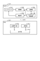
- FIG. 21 is a diagram illustrating a configuration example of an imaging element according to an eighth embodiment of the present disclosure
- FIG. 21 is a diagram illustrating a configuration example of an imaging element according to an eighth embodiment of the present disclosure
- FIG. FIG. 21 is a diagram illustrating a configuration example of an imaging element according to an eighth embodiment of the present disclosure
- FIG. 1 is a block diagram showing a configuration example of an imaging device mounted on an electronic device;
- FIG. 1 is a block diagram showing a configuration example of an imaging device mounted on an electronic device;
- FIG. 1 is a block diagram showing a configuration example of an imaging device mounted on an electronic device;
- FIG. 1 is a block diagram showing an example of a schematic configuration of a vehicle control system
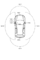
- FIG. FIG. 4 is an explanatory diagram showing an example of installation positions of an outside information detection unit and an imaging unit
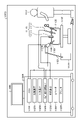
- 1 is a diagram showing an example of a schematic configuration of an endoscopic surgery system
- FIG. 3 is a block diagram showing an example of functional configurations of a camera head and a CCU;
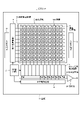
- FIG. 1 is a diagram showing a configuration example of an imaging device according to an embodiment of the present disclosure.
- the imaging device 1 of this example has a pixel region (so-called imaging region) 3 in which pixels 100 each including a plurality of photoelectric conversion elements are regularly arranged two-dimensionally on a semiconductor substrate 11, such as a silicon substrate. and a peripheral circuit section.
- the pixel 100 has, for example, a photodiode serving as a photoelectric conversion element and a plurality of pixel transistors (so-called MOS transistors).
- a plurality of pixel transistors can be composed of, for example, three transistors, a transfer transistor, a reset transistor, and an amplification transistor.
- Pixel 100 can also be a shared pixel structure.
- This pixel-sharing structure is composed of a plurality of photodiodes, a plurality of transfer transistors, one shared floating diffusion region, and one shared pixel transistor each.
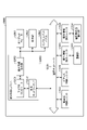
- the peripheral circuit section includes a vertical drive circuit 4, a column signal processing circuit 5, a horizontal drive circuit 6, an output circuit 7, a control circuit 8, and the like.
- the control circuit 8 receives an input clock and data instructing the operation mode, etc., and outputs data such as internal information of the imaging device. That is, the control circuit 8 generates a clock signal and a control signal that serve as a reference for the operation of the vertical driving circuit 4, the column signal processing circuit 5, the horizontal driving circuit 6, etc. based on the vertical synchronizing signal, the horizontal synchronizing signal, and the master clock. do. These signals are input to the vertical drive circuit 4, the column signal processing circuit 5, the horizontal drive circuit 6, and the like.
- the vertical drive circuit 4 is composed of, for example, a shift register, selects the pixel drive wiring 13, supplies a pulse for driving the pixels to the selected pixel drive wiring, and drives the pixels row by row. That is, the vertical driving circuit 4 sequentially selectively scans each pixel 100 in the pixel region 3 in the vertical direction on a row-by-row basis. A pixel signal based on the generated signal charge is supplied to the column signal processing circuit 5 .
- the column signal processing circuit 5 is arranged, for example, for each column of the pixels 100, and performs signal processing such as noise removal on the signals output from the pixels 100 of one row for each pixel column. That is, the column signal processing circuit 5 performs signal processing such as CDS (Correlated Double Sampling) for removing fixed pattern noise unique to the pixels 100, signal amplification, and AD conversion.
- a horizontal selection switch (not shown) is connected between the horizontal signal line 10 and the output stage of the column signal processing circuit 5 . Note that the column signal processing circuit 5 is an example of the processing circuit described in the claims.
- the horizontal driving circuit 6 is composed of, for example, a shift register, and sequentially outputs horizontal scanning pulses to select each of the column signal processing circuits 5 in turn, and outputs pixel signals from each of the column signal processing circuits 5 to the horizontal signal line. output to 10.
- the output circuit 7 performs signal processing on the signals sequentially supplied from each of the column signal processing circuits 5 through the horizontal signal line 10 and outputs the processed signals. For example, only buffering may be performed, or black level adjustment, column variation correction, and various digital signal processing may be performed.
- the input/output terminal 12 exchanges signals with the outside.
- FIG. 2 is a diagram illustrating a configuration example of a pixel according to an embodiment of the present disclosure
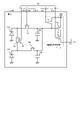
- the figure is a circuit diagram showing a configuration example of the pixel 100 according to the embodiment of the present disclosure.
- the pixel 100 includes photoelectric conversion units 101 and 102, charge holding units 103 and 104, charge transfer units 105 and 106, a reset transistor 111, an amplification transistor 112, a selection transistor 113, an overflow path 108, and an overflow gate. 109.
- a circuit configured by the reset transistor 111 , the amplification transistor 112 and the selection transistor 113 configures the image signal generator 110 .
- the charge transfer units 105 and 106, the reset transistor 111, the amplification transistor 112 and the selection transistor 113 can be configured by n-channel MOS transistors.
- the pixel driving wiring 13 and the vertical signal line 9 are wired to the pixel 100 .
- the pixel drive wiring 13 shown in the figure includes a signal line GATE, a signal line TRG1, a signal line TRG2, a signal line RST, and a signal line SEL.
- the vertical signal lines 9 also include the signal lines VO.
- the pixel 100 is wired with a power line Vdd.
- the power supply line Vdd is a wiring that supplies power to the pixels 100 .
- the anode of photoelectric conversion unit 101 is grounded, and the cathode is connected to the source of charge transfer unit 105 .
- the anode of photoelectric conversion unit 102 is grounded, and the cathode is connected to the source of charge transfer unit 106 .
- the drain of the charge transfer section 105 is connected to the source of the reset transistor 111 , the gate of the amplification transistor 112 , the drain of the charge transfer section 106 , one end of the charge holding section 103 and one end of the charge holding section 104 .
- the other end of charge holding portion 103 and the other end of 104 are grounded.
- a drain of the reset transistor 111 is connected to the power supply line Vdd.
- the amplification transistor 112 has a drain connected to the power supply line Vdd and a source connected to the drain of the selection transistor 113 .
- a source of the select transistor 113 is connected to the signal line VO.
- the overflow path 108 is connected between the cathode of the photoelectric conversion section 101 and the cathode of the photoelectric conversion section 102 .
- a signal line GATE, a signal line TRG1, and a signal line TRG2 are connected to the overflow gate 109, the gate of the charge transfer section 105, and the gate of the charge transfer section 106, respectively.
- a signal line RST and a signal line SEL are connected to the gate of the reset transistor 111 and the gate of the select transistor 113, respectively.
- the photoelectric conversion units 101 and 102 perform photoelectric conversion of incident light.
- the photoelectric conversion units 101 and 102 can be composed of photodiodes formed on a semiconductor substrate 120, which will be described later.
- the photoelectric conversion units 101 and 102 perform photoelectric conversion of incident light during an exposure period and hold charges generated by the photoelectric conversion.
- the charge holding units 103 and 104 hold charges generated by the photoelectric conversion units 101 and 102, respectively.
- the charge holding units 103 and 104 in the figure represent an example in which they are connected in parallel.
- the charge holding portions 103 and 104 can be configured by floating diffusion regions (FDs), which are semiconductor regions formed in the semiconductor substrate 120 .
- FDs floating diffusion regions
- the charge transfer units 105 and 106, the reset transistor 111, the amplification transistor 112 and the selection transistor 113 in the figure can be configured by n-channel MOS transistors.
- the drain-source can be made conductive by applying a voltage exceeding the threshold of the gate-source voltage Vgs to the gate.
- a voltage exceeding the threshold of the gate-source voltage Vgs is hereinafter referred to as an on-voltage.
- a control signal including this on-voltage is transmitted by a signal line TRG1 or the like.
- the charge transfer units 105 and 106 transfer charges.
- the charge transfer unit 105 transfers charges generated by photoelectric conversion of the photoelectric conversion unit 101 to the charge holding units 103 and 104
- the charge transfer unit 106 transfers charges generated by photoelectric conversion of the photoelectric conversion unit 102 to the charge holding unit 103 . and 104.
- the charge transfer units 105 and 106 transfer charges by establishing conduction between the photoelectric conversion units 101 and 102 and the charge holding units 103 and 104, respectively.
- Control signals for the charge transfer units 105 and 106 are transmitted by signal lines TRG1 and TRG2, respectively.
- the image signal generation unit 110 generates image signals based on the charges held in the charge holding units 103 and 104 .
- the image signal generator 110 is configured with the reset transistor 111 , the amplification transistor 112 and the selection transistor 113 .
- the reset transistor 111 resets the charge holding units 103 and 104 . This reset can be performed by conducting between the charge holding portions 103 and 104 and the power supply line Vdd to discharge the charges in the charge holding portions 103 and 104 . A control signal for the reset transistor 111 is transmitted through a signal line RST.
- the amplification transistor 112 amplifies the voltages of the charge holding units 103 and 104 .
- a gate of the amplification transistor 112 is connected to the charge holding portions 103 and 104 . Therefore, at the source of the amplifying transistor 112, an image signal having a voltage corresponding to the charges held in the charge holding portions 103 and 104 is generated.
- the selection transistor 113 By turning on the selection transistor 113, the image signal can be output to the signal line VO.
- a control signal for the select transistor 113 is transmitted by a signal line SEL.
- the overflow path 108 transfers charges overflowing between the photoelectric conversion units 101 and 102 to each other.
- This overflow path 108 can be configured by a semiconductor region arranged between the photoelectric conversion units 101 and 102 .
- the overflow gate 109 is an electrode arranged adjacent to the overflow path 108 . This overflow gate 109 adjusts the potential barrier of overflow path 108 .
- the charge transfer units 105 and 106 individually transfer the charges generated by the photoelectric conversion units 101 and 102 to the charge holding units 103 and 104 . This charge transfer is called individual transfer.
- the image signal generation unit 110 generates phase difference signals based on the charges individually transferred to the charge holding units 103 and 104 .
- the mode for generating the phase difference signal will be referred to as the phase difference signal mode.
- the charge transfer units 105 and 106 commonly transfer the charges generated by the photoelectric conversion units 101 and 102 to the charge holding units 103 and 104 .
- the charge holding units 103 and 104 collectively hold the charges generated by the photoelectric conversion units 101 and 102 at the same time. This charge transfer is referred to as collective transfer.
- a mode for generating this image signal is called an image signal mode.
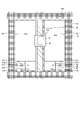
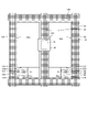
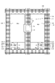
- FIG. 3 is a diagram illustrating a configuration example of a pixel according to the first embodiment of the present disclosure
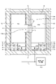
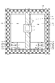
- the figure is a plan view showing a configuration example of the pixel 100 according to the first embodiment of the present disclosure.
- This drawing shows the configuration of the pixel 100 on the semiconductor substrate 120 .
- outline rectangles represent semiconductor regions formed in the semiconductor substrate 120 and gate electrodes arranged on the surface side of the semiconductor substrate 120 .
- Semiconductor regions 121 and 122 forming photoelectric conversion units 101 and 102 are arranged in the pixel 100
- charge transfer units 105 and 106 are arranged adjacent to the semiconductor regions 121 and 122 .
- gate electrodes 141 and 142 of charge transfer portions 105 and 106 are shown.
- Semiconductor regions 123 and 124 forming the charge holding portions 103 and 104 are arranged adjacent to the charge transfer portions 105 and 106 .
- An intra-pixel separation unit 128 is arranged between the photoelectric conversion units 101 and 102 .
- the intra-pixel separation section 128 separates the photoelectric conversion sections 101 and 102 .
- a pixel separation unit 129 is arranged at the boundary of the pixels 100 .
- the pixel separating portion 129 is configured in a shape surrounding the pixel 100 and separates the adjacent pixels 100 from each other.
- the image signal generation unit 110 is also shown in the figure.
- the figure shows an example in which the image signal generator 110 is arranged in a region other than the pixels 100 .
- the pixels in the figure are connected to the charge holding portions 103 and 104 by signal lines 119 .
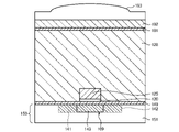
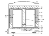
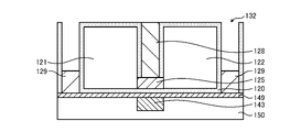
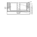
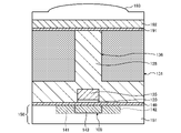
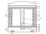
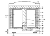
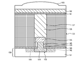
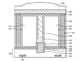
- FIG. 4A and 4B are cross-sectional views showing configuration examples of pixels according to the first embodiment of the present disclosure.
- 4A corresponds to a cross-sectional view of the pixel 100 along the line aa' in FIG. 3
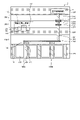
- FIG. 4B corresponds to the cross-sectional view of the pixel 100 along the bb' line in FIG.
- a pixel 100 in the figure includes a semiconductor substrate 120 , insulating films 149 and 191 , a wiring region 150 , a color filter 192 and an on-chip lens 193 .
- the semiconductor substrate 120 is a semiconductor substrate on which the diffusion layers of the elements of the pixel 100 are arranged.
- the semiconductor substrate 120 can be made of silicon (Si), for example.
- Elements such as the photoelectric conversion unit 101 can be arranged in a well region formed in the semiconductor substrate 120 .
- the semiconductor substrate 120 in the figure is configured as a p-type well region. By arranging an n-type or p-type semiconductor region in this well region, a diffusion layer of the device can be formed. Photoelectric conversion units 101 and 102 and an overflow path 108 are shown in FIG.
- the photoelectric conversion unit 101 is composed of an n-type semiconductor region 121 .
- a photodiode with a pn junction at the interface between the n-type semiconductor region 121 and the surrounding p-type well region corresponds to the photoelectric conversion unit 101 .
- the photoelectric conversion unit 102 is composed of an n-type semiconductor region 122 .
- Charges generated by photoelectric conversion of the photoelectric conversion units 101 and 102 during the exposure period are accumulated in the n-type semiconductor regions 121 and 122 .
- the accumulated charges are transferred to and held in the charge holding units 103 and 104 by the charge transfer units 105 and 106 after the exposure period has elapsed.
- An intra-pixel separation unit 128 is arranged between the photoelectric conversion units 101 and 102 .
- the in-pixel isolation portion 128 is composed of a semiconductor region having a relatively high p-type impurity concentration, and electrically isolates the n-type semiconductor regions 121 and 122 forming the photoelectric conversion portions 101 and 102 .
- a pixel separating portion 129 is arranged at the boundary of the pixels 100 on the semiconductor substrate 120 .
- the pixel isolation portion 129 is composed of a semiconductor region having a relatively high p-type impurity concentration, and electrically isolates adjacent pixels 100 from each other.
- the insulating film 149 is a film that insulates the surface side of the semiconductor substrate 120 .
- This insulating film 149 can be made of silicon oxide (SiO 2 ) or silicon nitride (SiN).
- Gate electrodes 141 , 142 and 143 are arranged on the surface side of the semiconductor substrate 120 . Gate electrodes 141 and 142 form the gates of charge transfer sections 105 and 106, respectively. Gate electrode 143 forms overflow gate 109 . This overflow gate 109 adjusts the potential barrier of the overflow path 108 . By applying a voltage to the overflow gate 109, the height of the potential barrier of the overflow path 108 can be adjusted.
- the gate electrodes 141, 142 and 143 can be made of polycrystalline silicon.
- the insulating film 149 under the gate electrodes 141, 142 and 143 forms a gate insulating film.
- the wiring region 150 is arranged on the surface side of the semiconductor substrate 120 and is a region where the wiring of the pixels 100 is arranged.
- the wiring region 150 includes wiring 152 and an insulating layer 151 .
- the wiring 152 transmits signals and the like of the elements of the pixel 100 .
- This wiring 152 can be made of a conductor such as copper (Cu) or tungsten (W).
- the insulating layer 151 insulates the wiring 152 and the like.
- This insulating layer 151 can be made of, for example, SiO 2 .
- the insulating film 191 insulates the back side of the semiconductor substrate 120 .
- This insulating film 191 can be made of, for example, SiO 2 .
- the color filter 192 is an optical filter that transmits light of a predetermined wavelength among incident light.
- a color filter that transmits red light, green light and blue light can be used.
- the on-chip lens 193 is a lens that collects incident light. This on-chip lens 193 is configured in a hemispherical shape and converges incident light onto the photoelectric conversion units 101 and 102 .
- the amount of charge that can be stored in the n-type semiconductor regions 121 and 122 is limited. This storable charge amount is called a saturated charge amount Qs. This Qs changes depending on the size of the n-type semiconductor region 121 and the like, and the charges generated exceeding Qs overflow from the n-type semiconductor region 121 and the like. If the overflowed charges flow into the photoelectric conversion units 101 of other pixels 100 and the like to generate image signals, errors will occur in the image signals. Therefore, the charge that overflows from the photoelectric conversion unit 101 or the like is discharged to the charge holding unit 103 or the like of the pixel 100 itself.
- the charges discharged to the charge holding unit 103 and the like during the exposure period are discharged by resetting after the exposure period has elapsed.
- photoelectric conversion units 101 and 102 are arranged in the pixel 100 in FIG.
- Charge overflow also occurs when the charge in either of the photoelectric conversion units 101 and 102 exceeds Qs.
- This overflowing charge flows into the charge holding portion 103 and the like. Since this charge is discharged by resetting after the exposure period has elapsed, an error occurs in the image signal in the image signal mode in which the image signal is generated by summing the charges generated by the photoelectric conversion units 101 and 102. . This is because charges overflowing from one of the photoelectric conversion units 101 and 102 are not reflected in the combined image signal, and the linearity of the characteristics of the image signal voltage with respect to the amount of light incident on the pixel 100 is degraded.
- an overflow path 108 is arranged between the photoelectric conversion units 101 and 102 .
- This overflow path 108 is composed of an n-type semiconductor region 125 .
- the overflow path 108 is configured as a potential barrier lower than the potential barrier of the charge transfer section 105 and the like, and can transfer charges overflowing from the photoelectric conversion sections 101 and 102 to each other. For example, when the charge of the photoelectric conversion unit 101 reaches Qs while the charge of the photoelectric conversion unit 102 does not reach Qs, photoelectric conversion is performed from the n-type semiconductor region 121 of the photoelectric conversion unit 101 through the overflow path 108 . Charge moves to the n-type semiconductor region 122 of the portion 102 .
- the overflow path 108 it is possible to reduce the error of the image signal when the charges of the photoelectric conversion units 101 and 102 are added.
- the potential barrier of the overflow path 108 is lowered, so the amount of charge that can be accumulated in each of the photoelectric conversion units 101 and 102 is lower than Qs.
- the maximum value of the signal level of the phase difference signal is lowered. For this reason, the detectable phase difference range of the object is narrowed. Therefore, overflow gate 109 is placed adjacent to overflow path 108 . By applying a voltage to the overflow gate 109, it is possible to adjust the potential of the overflow path 108 and adjust the potential barrier.
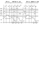
- FIG. 5 is a diagram illustrating an example of generation of an image signal and a phase difference signal according to an embodiment of the present disclosure; The figure is a timing chart showing an example of generation of an image signal and a phase difference signal in the pixel 100.
- FIG. 5 is a diagram illustrating an example of generation of an image signal and a phase difference signal according to an embodiment of the present disclosure. The figure is a timing chart showing an example of generation of an image signal and a phase difference signal in the pixel 100.
- RST, SEL, TRG1”, “TRG2” and “GATE” in the figure represent signals of the signal line RST, signal line SEL, signal line TRG1, signal line TRG2 and signal line GATE, respectively. These represent the waveforms of the binarized control signals, and the portion of the value "1" represents the region to which the ON signal is transmitted. Also, the dashed line represents the level of 0V. Also, “FD” represents the potential of the charge holding portions 103 and 104 . Also, “VO” represents the output of the signal line VO. The first half of the figure represents the procedure for the phase difference signal mode, and the latter half represents the procedure for the image signal mode.
- the value "0" is applied to the signal line RST, signal line SEL, signal line TRG1, and signal line TRG2.
- a negative gate voltage is applied to the signal line GATE.
- an ON signal is applied to the signal lines RST, TRG1 and TRG2.
- the reset transistor 111 and the charge transfer units 105 and 106 become conductive, and the photoelectric conversion units 101 and 102 and the charge holding units 103 and 104 are reset.
- a positive gate voltage is applied to the signal line GATE. Thereby, the potential barrier of the overflow path 108 can be lowered.
- an ON signal is applied to the signal line SEL.
- the application of the ON signal to the signal line SEL continues until the phase difference signals of all the pixels 100 in the pixel region 3 are output.
- an ON signal is applied to the signal line TRG1.
- the charge transfer unit 105 becomes conductive, and the charges accumulated in the photoelectric conversion unit 101 are transferred to the charge holding units 103 and 104 . This lowers the potential of the FD.
- the ON signal to the signal line TRG1 is stopped.
- the image signal b corresponding to the charge of the photoelectric conversion unit 101 is output from the signal line VO.
- the CDS described above is performed by the image signal a and the image signal b to generate a phase difference signal.
- an ON signal is applied to the signal line RST, and the charge holding units 103 and 104 are reset.
- an ON signal is applied to the signal line TRG2.
- the charge transfer unit 106 becomes conductive, and the charges accumulated in the photoelectric conversion unit 102 are transferred to the charge holding units 103 and 104 . This lowers the potential of the FD.
- phase difference signals can be generated in the phase difference signal mode.
- image signal mode will be explained.
- an ON signal is applied to the signal lines RST, TRG1 and TRG2.
- the reset transistor 111 and the charge transfer units 105 and 106 become conductive, and the photoelectric conversion units 101 and 102 and the charge holding units 103 and 104 are reset.
- a positive gate voltage is applied to the signal line GATE. Thereby, the potential barrier of the overflow path 108 can be lowered.
- a negative gate voltage is applied to the signal line GATE.
- an ON signal is applied to the signal line SEL.
- the application of the ON signal to the signal line SEL continues until the image signals of all the pixels 100 in the pixel region 3 are output.
- an ON signal is applied to the signal lines TRG1 and TRG2.
- the charge transfer units 105 and 106 become conductive, and charges accumulated in the photoelectric conversion units 101 and 102 are transferred to the charge holding units 103 and 104 . This lowers the potential of the FD.
- the gate voltage of the signal line GATE in T3-T4 in the phase difference signal mode and the gate voltage of the signal line GATE in T16-T17 in the image signal mode can be set to different values. Specifically, the gate voltage in T3-T4 can be set to a low voltage. This makes it possible to make the potential barrier of the overflow path 108 higher in the phase difference signal mode than in the image signal mode.
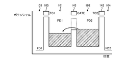
- FIG. 6A is a diagram showing potential barriers of the photoelectric conversion units 101 and 102, the charge transfer units 105 and 106, the charge retention units 103 and 104, and the overflow path 108 of the pixel 100.
- FIG. The horizontal axis represents the position in the pixel 100, and the vertical axis represents the potential.
- "FD1”, “TG1”, “PD1”, “GATE”, “PD2”, “TG2” and “FD2" represent the positions described in FIG.
- a high potential barrier is formed in the charge transfer portions 105 and 106 during the exposure period. As a result, charges are accumulated in the photoelectric conversion units 101 and 102 .
- the hatched rectangles in the figure represent charges that are accumulated.
- a high gate voltage is applied to the overflow gate 109, and the potential barrier of the overflow path 108 becomes relatively low. Therefore, as shown in FIG. 6A, charges overflowing from the photoelectric conversion unit 102 are transferred to the photoelectric conversion unit 101 through the overflow path 108 .
- a dotted line potential barrier of the overflow path 108 represents a potential barrier when no gate voltage is applied to the overflow gate 109 .
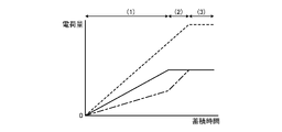
- FIG. 6B is a diagram showing the relationship between charge accumulation time and charge amount in the image signal mode.
- the horizontal axis represents the accumulation time
- the vertical axis represents the charge amount.
- the solid-line graph in FIG. 6A is a graph representing the change in the charge amount of the photoelectric conversion unit 102 in FIG. 6A.
- the dashed-dotted line graph in FIG. 6A is a graph showing changes in the amount of charge in the photoelectric conversion unit 101 in FIG. 6A.
- the dotted line graph in FIG. 2 is a graph showing the charge amount obtained by adding the charges of the photoelectric conversion units 101 and 102 .
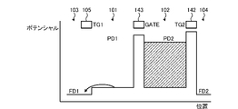
- FIG. 6C shows the potential barrier in the phase difference signal mode.
- the charges of the photoelectric conversion units 101 and 102 are individually transferred to the charge holding units 103 and 104 .
- This figure shows an example of transferring the charge of the photoelectric conversion unit 101 .
- the voltage applied to the gate electrode may modulate the potential of the overflow path 108 and lower the potential barrier of the overflow path 108 .
- the vertical drive circuit 3 By applying a negative gate voltage to the overflow gate 109 , the potential barrier of the overflow path 108 can be prevented from lowering, and the charge transfer from the photoelectric conversion unit 102 to the photoelectric conversion unit 101 can be prevented.
- Such gate voltage adjustment is performed by the vertical drive circuit 3 .
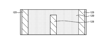
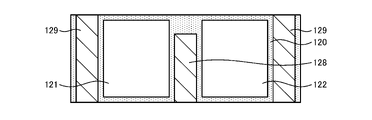
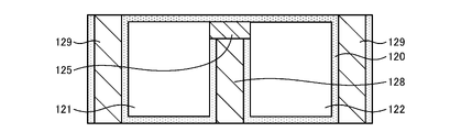
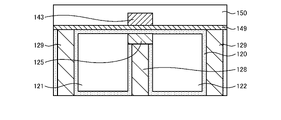
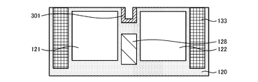
- FIG. 7A-7D are diagrams illustrating an example of a method for manufacturing an imaging device according to the first embodiment of the present disclosure.
- 7A-7D are diagrams showing an example of the manufacturing process of the pixel 100 portion of the imaging device 1.
- FIG. 7A-7D are diagrams showing an example of the manufacturing process of the pixel 100 portion of the imaging device 1.
- a well region is formed in the semiconductor substrate 120, and an intra-pixel isolation portion 128 and a pixel isolation portion 129 are formed (FIG. 7A). This can be done by ion implantation of impurities. At this time, in the ion implantation, an acceptor impurity is implanted to make the p-type, which is the same conductivity type as the well region.
- the photoelectric conversion section 101 and the like are formed on the semiconductor substrate 120 .
- n-type semiconductor regions 121 and 122 and the like are formed in a semiconductor substrate 120 . This can be done by ion implantation of impurities (FIG. 7B).
- a semiconductor region 125 forming the overflow path 108 is formed in the semiconductor substrate 120 . This can be done by ion implantation of impurities (FIG. 7C).
- an insulating film 149 is formed on the surface side of the semiconductor substrate 120, and a gate electrode 143 forming the overflow gate 109 is arranged.
- a wiring region 150 is formed on the surface side of the semiconductor substrate 120 (FIG. 7D).
- the back side of the semiconductor substrate 120 is ground to be thinned.
- the pixel 100 can be manufactured by arranging the insulating film 191 , the color filter 192 and the on-chip lens 193 on the back side of the semiconductor substrate 120 .
- FIG. 8 is a diagram showing an example of gate voltage measurement of the overflow gate according to the first embodiment of the present disclosure.
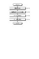
- FIG. 8 is a flow chart showing an example of measurement of the gate voltage of the overflow gate 109 in the manufacturing process of the imaging device 1.
- step S101 the amount of electric charge is measured for each of the photoelectric conversion units 101 and 102 of the pixel 100 of the manufactured image sensor 1. This can be done by measuring the Qs of the photoelectric conversion units 101 and 102 .
- the inter-pixel potential is measured (step S102). This can be done by measuring the potential between pixels 100 .
- the gate voltage is detected (step S103).
- step S104 This can be done by holding the detected gate voltage in a holding unit such as a register arranged in the imaging device 1 .
- a desired characteristic can be obtained by applying the gate voltage read from the register to the overflow gate 109 when the imaging device 1 is used.
- the pixel 100 of the present disclosure arranges the overflow gate 109 adjacent to the overflow path 108 arranged between the plurality of photoelectric conversion units 101 and 102, and adjusts the voltage applied to the overflow gate 109.
- This makes it possible to adjust the potential barrier of the overflow path 108, improve the linearity of the image signal, and widen the phase difference detectable range when generating the phase difference signal. Convenience can be improved.
- the imaging device 1 of the first embodiment described above the pixel separation section 129 formed of a semiconductor region is arranged at the boundary between the pixels 100 .
- the imaging device 1 of the second embodiment of the present disclosure differs from the above-described first embodiment in that a pixel separating section made of an insulating material is arranged.
- FIG. 9 is a diagram showing a configuration example of the pixel 100 according to the second embodiment of the present disclosure. This figure, like FIG. 3, is a plan view showing a configuration example of the imaging element 1. As shown in FIG. A pixel 100 in FIG. 3 differs from the pixel 100 in FIG. 3 in that a pixel separation section 131 is provided instead of the pixel separation section 129 .
- the pixel separation section 131 is a pixel separation section configured by embedding an insulating member in the semiconductor substrate 120 .
- the pixel separating portion 131 can be formed by embedding an insulating film such as SiO 2 in a groove portion 132 formed in the semiconductor substrate 120 .
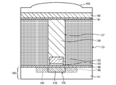
- FIGS. 10A and 10B are cross-sectional views showing configuration examples of pixels according to the second embodiment of the present disclosure. Similar to FIGS. 4A and 4B, FIGS. 10A and 10B are cross-sectional views showing configuration examples of the pixel 100.
- FIG. Pixel 100 of FIGS. 10A and 10B differs from pixel 100 of FIGS. 4A and 4B in that pixel separator 131 is arranged instead of pixel separator 129 .
- the pixel separation section 131 can be configured by arranging an insulating film in a groove section 132 formed from the rear surface side of the semiconductor substrate 120 at the boundary of the pixels 100 .
- FIGS. 7A-7D are diagrams illustrating an example of a method for manufacturing an imaging device according to the second embodiment of the present disclosure.
- 11A and 11B are diagrams showing an example of the manufacturing process of the pixel 100 portion of the image sensor 1.
- FIG. 1 the steps of FIGS. 7A-7D are performed.
- the imaging device 1 is turned upside down, and a groove portion 132 is formed from the back side of the semiconductor substrate 120 (FIG. 11A). This can be done, for example, by dry etching.
- an insulating member such as SiO 2 is placed in the groove 132 . This can be done, for example, by CVD (FIG. 11B). Thereby, the pixel separating portion 131 can be formed.
- the configuration of the imaging device 1 other than this is the same as the configuration of the imaging device 1 in the first embodiment of the present disclosure, the description is omitted.
- the image pickup device 1 of the second embodiment of the present disclosure can improve insulation characteristics between the pixels 100 by arranging the pixel separation section 131 configured by an insulating member.
- the pixel separation section 131 is arranged in which an insulating material is embedded in the groove section 132 formed from the rear surface side of the semiconductor substrate 120 at the boundary between the pixels 100 .
- the imaging device 1 of the third embodiment of the present disclosure has a pixel separation section configured by embedding an insulator in a groove formed from the surface of the semiconductor substrate 120, and is different from the above-described third embodiment. 2 embodiment.
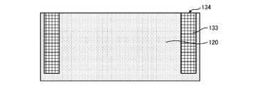
- FIG. 12 is a diagram showing a configuration example of the pixel 100 according to the third embodiment of the present disclosure.
- This figure like FIG. 9, is a plan view showing a configuration example of the imaging device 1.
- a pixel 100 in the figure differs from the pixel 100 in FIG. 9 in that a pixel separation section 133 is provided instead of the pixel separation section 131 .
- the pixel separation section 133 is a pixel separation section configured by embedding an insulating member in the semiconductor substrate 120 .
- the pixel separating portion 133 can be formed by embedding an insulating film such as SiO 2 in a groove portion 134 formed in the semiconductor substrate 120 .
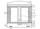
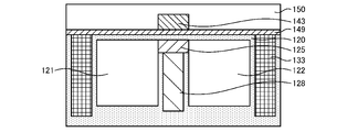
- FIGS. 13A and 13B are cross-sectional views showing configuration examples of pixels according to the third embodiment of the present disclosure.
- 13A and 13B are cross-sectional views showing configuration examples of the pixel 100, similar to FIGS. 10A and 10B.
- Pixel 100 in FIGS. 13A and 13B differs from pixel 100 in FIGS. 10A and 10B in that pixel separator 133 is arranged instead of pixel separator 131 .
- the pixel separating portion 133 is formed in a shape penetrating the semiconductor substrate 120 .
- the groove portion 134 is a groove portion formed from the surface of the semiconductor substrate 120 at the boundary of the pixel 100 .
- a pixel separating portion 133 can be formed by arranging an insulating film in the groove portion 134 .
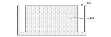
- FIG. 14A and 14D are diagrams illustrating an example of a method for manufacturing an imaging device according to the third embodiment of the present disclosure.
- 14A and 14D are diagrams showing an example of the manufacturing process of the pixel 100 portion of the image sensor 1.
- a pixel separating portion 133 is formed by embedding an insulating film such as SiO 2 in the groove portion 134 (FIG. 14B).
- the intra-pixel isolation section 128, the semiconductor regions 121 and 122, the semiconductor region 125, the insulating film 149, the gate electrode 143 and the wiring region 150 are formed (FIG. 14C).
- the back side of the semiconductor substrate 120 is ground to thin it (FIG. 14D). Thereby, the pixel isolation part 133 having a shape penetrating the semiconductor substrate 120 can be formed.
- the configuration of the imaging device 1 other than this is the same as the configuration of the imaging device 1 according to the second embodiment of the present disclosure, so the description is omitted.
- the imaging device 1 of the third embodiment of the present disclosure includes the pixel separation section 133 having a shape penetrating through the semiconductor substrate 120 .
- the insulating properties between the pixels 100 on the surface side of the semiconductor substrate 120 can be further improved.
- the imaging device 1 of the second embodiment described above the pixel separating section 131 is arranged at the boundary between the pixels 100 .
- the imaging device 1 of the fourth embodiment of the present disclosure is different from the above-described second embodiment in that an isolation portion made of an insulating material is further arranged between the photoelectric conversion portions 101 and 102 of the pixel 100. Different from the form.
- FIG. 15 is a diagram showing a configuration example of the pixel 100 according to the fourth embodiment of the present disclosure. This figure, like FIG. 9, is a plan view showing a configuration example of the imaging device 1. As shown in FIG. A pixel 100 in FIG. 9 differs from the pixel 100 in FIG. 9 in that an intra-pixel separation section 135 is further provided.
- the in-pixel separation section 135 is a separation section arranged between the photoelectric conversion sections 101 and 102 and is a separation section formed by embedding an insulating member in a groove formed in the semiconductor substrate 120 .
- the groove portion 134 in the figure is also formed between the photoelectric conversion portions 101 and 102 in addition to the boundary of the pixel 100 .
- the intra-pixel separation portion 135 can be formed by embedding an insulating film similar to the pixel separation portion 131 in the groove portion 134 between the photoelectric conversion portions 101 and 102 .
- 16A and 16B are cross-sectional views showing configuration examples of pixels according to the fourth embodiment of the present disclosure.
- 16A and 16B are cross-sectional views showing configuration examples of the pixel 100, similar to FIGS. 10A and 10B.
- the pixel 100 of FIGS. 16A and 16B differs from the pixel 100 of FIGS. 10A and 10B in that an intra-pixel separator 135 is further provided.
- an intra-pixel isolation portion 128 is arranged in the semiconductor substrate 120 below the overflow path 108 .
- the intra-pixel separating section 128 is an example of the second intra-pixel separating section described in the claims.
- FIG. 17 is a diagram showing another configuration example of the pixel 100 according to the fourth embodiment of the present disclosure. Similar to FIG. 16, this figure is a plan view showing a configuration example of the imaging element 1. As shown in FIG. A pixel 100 in FIG. 16 differs from the pixel 100 in FIG. 16 in that a pixel separation section 133 and an intra-pixel separation section 137 are provided instead of the pixel separation section 131 and the intra-pixel separation section 135 .
- the in-pixel separation portion 137 is a separation portion having a shape penetrating through the semiconductor substrate 120 in the same manner as the pixel separation portion 133 .
- FIGS. 18A and 18B are cross-sectional views showing other configuration examples of pixels according to the fourth embodiment of the present disclosure.
- 18A and 18B are cross-sectional views showing configuration examples of the pixel 100, similar to FIGS. 10A and 10B.
- Pixel 100 in FIGS. 18A and 18B differs from pixel 100 in FIGS. 10A and 10B in that pixel separator 133 and intra-pixel separator 137 are provided instead of pixel separator 131 and intra-pixel separator 135 .
- the in-pixel isolation portion 137 is formed in a shape penetrating the semiconductor substrate 120 .
- an intra-pixel isolation portion 128 is arranged in the semiconductor substrate 120 below the overflow path 108 .
- the configuration of the imaging device 1 other than this is the same as the configuration of the imaging device 1 according to the second embodiment of the present disclosure, so the description is omitted.
- the imaging device 1 includes the intra-pixel separation sections 135 and 137 made of insulating members. Thereby, the insulation characteristics between the photoelectric conversion units 101 and 102 can be improved.
- the overflow path 108 and the overflow gate 109 are arranged in the center of the pixel 100 .
- the image sensor 1 of the fifth embodiment of the present disclosure differs from the above-described first embodiment in that the overflow path 108 and the overflow gate 109 are arranged near the edge of the pixel 100 .
- FIG. 19 is a diagram showing a configuration example of the pixel 100 according to the fifth embodiment of the present disclosure. This figure, like FIG. 3, is a plan view showing a configuration example of the imaging element 1. As shown in FIG. Pixel 100 in FIG. 3 differs from pixel 100 in FIG. 3 in that overflow path 108 and overflow gate 109 are located near the edges of pixel 100 .
- An overflow path 108 and an overflow gate 109 in the figure are arranged near the edge of the pixel 100 and separated from the charge transfer sections 105 and 106 . That is, the overflow path 108, the overflow gate 109, and the charge transfer units 105 and 106 are arranged near the boundaries of the pixels 100 facing each other. Since the overflow path 108 is arranged apart from the charge transfer sections 105 and 106, the potential modulation of the overflow path 108 described in FIG. 6C can be reduced.
- the configuration of the imaging device 1 other than this is the same as the configuration of the imaging device 1 in the first embodiment of the present disclosure, the description is omitted.
- the overflow path 108 is arranged apart from the charge transfer sections 105 and 106, the gate voltage of the charge transfer sections 105 and 106 with respect to the overflow path 108 is can reduce the impact of
- the overflow gate 109 is arranged on the surface side of the semiconductor substrate 120 .
- the imaging device 1 of the sixth embodiment of the present disclosure differs from the above-described fourth embodiment in that overflow gates embedded in the semiconductor substrate 120 are arranged.
- FIG. 20 is a diagram showing a configuration example of the pixel 100 according to the sixth embodiment of the present disclosure. Similar to FIG. 17, this figure is a plan view showing a configuration example of the imaging element 1. As shown in FIG. A pixel 100 in FIG. 17 differs from the pixel 100 in FIG. 17 in that it includes an overflow gate 109 composed of a gate electrode 144 .
- the overflow gate 109 in the same figure has a gate electrode 144 .
- the gate electrode 144 is a gate electrode at least partially embedded in the semiconductor substrate 120 .
- 21A and 21B are cross-sectional views showing configuration examples of pixels according to the sixth embodiment of the present disclosure.
- 21A and 21B are cross-sectional views showing configuration examples of the pixel 100, similar to FIGS. 18A and 18B.
- Pixel 100 of FIGS. 21A and 21B differs from pixel 100 of FIGS. 18A and 18B in that overflow gate 109 with gate electrode 144 is arranged instead of gate electrode 143 .
- the gate electrode 144 is configured such that the lower portion thereof is embedded in the semiconductor substrate 120 .
- the overflow path 108 in the same figure can be arranged in a layer below the gate electrode 144 .
- Overflow path 108 can be isolated from charge transfer sections 105 and 106 .
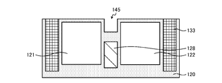
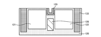
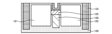
- FIG. 22A-22E are diagrams illustrating an example of a method for manufacturing an imaging device according to the sixth embodiment of the present disclosure. 22A-22E are diagrams showing an example of the manufacturing process of the pixel 100 portion of the imaging device 1.
- an in-pixel isolation portion 128 is formed on the semiconductor substrate 120 .
- semiconductor regions 121 and 122 are formed in the semiconductor substrate 120 .
- an opening 145 is formed on the surface side of the semiconductor substrate 120 . This can be done by dry etching (Fig. 22A).
- a film 301 such as SiO 2 is placed in the opening 145 (FIG. 22B).
- This film 301 is called a so-called sacrificial film.
- ion implantation is performed through the film 301 to form a p-type semiconductor region 129 in the semiconductor substrate 120 on the bottom and side surfaces of the opening 145 (FIG. 22C).
- the semiconductor region 125 of the overflow path 108 is formed (FIG. 22D). This can be done by ion implantation.
- the film 301 is peeled off.
- a gate oxide film is then placed in the opening 145 .
- a gate electrode member is placed in the opening 145 to form the gate electrode 144 (FIG. 22E).
- the gate electrode 144 can be formed through the above steps.
- the semiconductor region 129 formed in FIG. 22C is arranged in order to prevent the potential from being modulated by the gate electrode 144 in areas other than the overflow path 108 to form an unintended electron path. Also, by arranging this semiconductor region 129, it is possible to suppress the generation of dark current due to the defect level of the wall surface of the opening 145. FIG.
- the configuration of the imaging device 1 other than this is the same as the configuration of the imaging device 1 according to the fourth embodiment of the present disclosure, so the description is omitted.
- the imaging device 1 of the sixth embodiment of the present disclosure includes the overflow gate 109 having the gate electrode 144 at least partially embedded in the semiconductor substrate 120 . Thereby, the influence of the charge transfer units 105 and 106 on the overflow path 108 can be reduced.
- the gate electrode 144 embedded in the semiconductor substrate 120 is arranged.
- the imaging element 1 of the seventh embodiment of the present disclosure differs from the sixth embodiment described above in that a buried insulating film is arranged around the gate electrode 144 .
- FIG. 23 is a diagram showing a configuration example of the pixel 100 according to the seventh embodiment of the present disclosure. This figure is a plan view showing a configuration example of the imaging element 1, like FIG. The pixel 100 shown in the figure differs from the pixel 100 shown in FIG. 20 in that a buried insulating film is arranged around the gate electrode 144 .
- FIGS. 24A and 24B are cross-sectional views showing configuration examples of pixels according to the seventh embodiment of the present disclosure.
- 24A and 24B are cross-sectional views showing configuration examples of the pixel 100, similar to FIGS. 21A and 21B.
- the pixel 100 of FIGS. 24A and 24B differs from the pixel 100 of FIGS. 21A and 21B in that a buried insulating film 138 is arranged around the gate electrode 144.
- FIG. As shown in the figure, the embedded insulating film 138 is arranged around the gate electrode 144 embedded in the semiconductor substrate 120 .
- Such a buried insulating film 138 is called STI (Shallow Trench Isolation).
- This STI can be formed by forming an opening in the semiconductor substrate 120 and embedding an insulating film.
- the embedded insulating film 138 can be arranged around the gate electrode 144 . Since the side surface of the gate electrode 144 is insulated by the buried insulating film 138, it is possible to prevent the potential barrier other than the overflow path 108 from being modulated by the gate electrode 144. FIG. Controllability of the potential barrier of the overflow path 108 can be improved.
- a semiconductor region 129 or the like can be arranged as described in FIG. 22C.
- the embedded insulating film 138 is an example of the separating portion described in the claims.
- the configuration of the imaging device 1 other than this is the same as the configuration of the imaging device 1 according to the sixth embodiment of the present disclosure, so the description is omitted.
- the imaging device 1 of the seventh embodiment of the present disclosure has the buried insulating film 138 arranged around the gate electrode 144 to prevent the potential barrier other than the overflow path 108 from being modulated by the gate electrode 144. be able to. Controllability of the potential barrier of the overflow path 108 can be improved.
- the imaging device 1 of the above-described first embodiment was configured with the semiconductor substrate 120 .
- the imaging element 1 of the eighth embodiment of the present disclosure differs from the first embodiment described above in that it is configured by stacking a plurality of semiconductor substrates.
- FIG. 25 is a diagram illustrating a configuration example of an imaging element according to the eighth embodiment of the present disclosure; This figure is a cross-sectional view showing a configuration example of the imaging device 1 .
- the image pickup device 1 in FIG. 1 is different from the image pickup device 1 in FIG. 1 in that semiconductor substrates 220 and 320 are laminated on a semiconductor substrate 120 .
- the photoelectric conversion units 101 and 102, the charge transfer units 105 and 106 (not shown), and the charge holding units 103 and 104 (not shown) of the pixel 100 are arranged. Also, the overflow path 108 and the overflow gate 109 of the pixel 100 are arranged on the semiconductor substrate 120 . note that. Pixels 100a and 100b are described on the semiconductor substrate 120 in the figure.
- a wiring 152 is shown in the wiring area 150 in the figure.
- the wiring 152 is commonly connected to the gate electrodes 143 of the pixels 100a and 100b.
- the wiring 152 can be made of, for example, impurity-implanted polycrystalline silicon.
- the semiconductor substrate 220 is a semiconductor substrate that has a wiring region 250 and is laminated on the semiconductor substrate 120 .
- the image signal generator 110 is arranged on the semiconductor substrate 220 .
- the amplification transistor 112 is described as an example.
- the amplifying transistor 112 is composed of semiconductor regions 221 and 222 formed in a semiconductor substrate 220 and a gate electrode 242 .
- the wiring region 250 includes an insulating layer 251 , wiring 252 , via plugs 253 and connection pads 259 .
- the connection pads 259 are electrically connected to connection pads 359 in the wiring region 350 of the semiconductor substrate 320, which will be described later.
- a through via 154 for connecting the semiconductor substrate 120 and the semiconductor substrate 220 is arranged.
- a through via 154 in the figure connects the wirings 152 and 252 .
- the through via 154 can be made of columnar tungsten (W) or the like.
- the semiconductor substrate 320 is a semiconductor substrate having a wiring region 350 and laminated on the semiconductor substrate 220 .
- the vertical driving circuit 4 and the like are arranged on the semiconductor substrate 320 .
- an insulating layer 351, wiring 352, via plugs 354 and connection pads 359 are arranged.
- the gate voltage of the gate electrode 143 of the overflow gate 109 is supplied from the vertical driving circuit 4 via the wiring 152, the through via 154, the wiring 252, the via plug 253, the connection pads 259 and 359, and the via plug 354.
- the number of through vias 154 can be reduced.
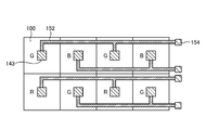
- FIGS. 26A and 26B are diagrams showing configuration examples of an imaging device according to the eighth embodiment of the present disclosure.
- 26A and 26B are plan views showing an arrangement example of the wiring 152 on the semiconductor substrate 120.
- FIG. Four pixels 100 are described in FIGS. 26A and 26B. The descriptions of “R”, “G” and “B” of these pixels 100 represent the types of color filters 192 .
- FIG. 26A shows an example in which the gate electrodes 143 of the pixels 100 in which the same type of color filters 192 are arranged are commonly connected to the same wiring 152.
- FIG. A gate voltage is applied to the gate electrode 143 at a common timing in the pixels 100 in which the same type of color filters 192 are arranged. Therefore, the gate voltage of these pixels 100 is supplied from the common wiring 152 .
- FIG. 26B shows an example in which the wiring 152 is commonly connected to the gate electrodes 143 of eight pixels 100 .
- the number of through vias 154 can be further reduced.
- the imaging device 1 as described above can be applied to various electronic devices such as imaging systems such as digital still cameras and digital video cameras, mobile phones with imaging functions, and other devices with imaging functions. can be done.
- FIG. 27 is a block diagram showing a configuration example of an imaging device mounted on an electronic device.
- an imaging device 701 includes an optical system 702, an imaging device 703, and a DSP (Digital Signal Processor) 704. , a recording device 709, and a power supply system 710 are connected, and can capture still images and moving images.
- DSP Digital Signal Processor
- the optical system 702 is configured with one or more lenses, guides image light (incident light) from the subject to the imaging element 703, and forms an image on the light receiving surface (sensor section) of the imaging element 703.
- the image pickup device 703 As the image pickup device 703, the image pickup device 1 having any of the configuration examples described above is applied. Electrons are accumulated in the imaging element 703 for a certain period of time according to the image formed on the light receiving surface via the optical system 702 . A signal corresponding to the electrons accumulated in the image sensor 703 is input to the DSP 704 .
- the DSP 704 performs various signal processing on the signal from the image sensor 703 to obtain an image, and temporarily stores the image data in the memory 708 .
- the image data stored in the memory 708 is recorded in the recording device 709 or supplied to the display device 705 to display the image.
- An operation system 706 receives various operations by a user and supplies an operation signal to each block of the imaging apparatus 701 , and a power supply system 710 supplies electric power necessary for driving each block of the imaging apparatus 701 .
- the technology (the present technology) according to the present disclosure can be applied to various products.
- the technology according to the present disclosure can be realized as a device mounted on any type of moving body such as automobiles, electric vehicles, hybrid electric vehicles, motorcycles, bicycles, personal mobility, airplanes, drones, ships, and robots. may
- FIG. 28 is a block diagram showing a schematic configuration example of a vehicle control system, which is an example of a mobile control system to which the technology according to the present disclosure can be applied.
- a vehicle control system 12000 includes a plurality of electronic control units connected via a communication network 12001.
- the vehicle control system 12000 includes a drive system control unit 12010, a body system control unit 12020, an exterior information detection unit 12030, an interior information detection unit 12040, and an integrated control unit 12050.
- a microcomputer 12051, an audio/image output unit 12052, and an in-vehicle network I/F (Interface) 12053 are illustrated.
- the drive system control unit 12010 controls the operation of devices related to the drive system of the vehicle according to various programs.
- the driving system control unit 12010 includes a driving force generator for generating driving force of the vehicle such as an internal combustion engine or a driving motor, a driving force transmission mechanism for transmitting the driving force to the wheels, and a steering angle of the vehicle. It functions as a control device such as a steering mechanism to adjust and a brake device to generate braking force of the vehicle.
- the body system control unit 12020 controls the operation of various devices equipped on the vehicle body according to various programs.
- the body system control unit 12020 functions as a keyless entry system, a smart key system, a power window device, or a control device for various lamps such as headlamps, back lamps, brake lamps, winkers or fog lamps.
- the body system control unit 12020 can receive radio waves transmitted from a portable device that substitutes for a key or signals from various switches.
- the body system control unit 12020 receives the input of these radio waves or signals and controls the door lock device, power window device, lamps, etc. of the vehicle.
- the vehicle exterior information detection unit 12030 detects information outside the vehicle in which the vehicle control system 12000 is installed.
- the vehicle exterior information detection unit 12030 is connected with an imaging section 12031 .
- the vehicle exterior information detection unit 12030 causes the imaging unit 12031 to capture an image of the exterior of the vehicle, and receives the captured image.
- the vehicle exterior information detection unit 12030 may perform object detection processing or distance detection processing such as people, vehicles, obstacles, signs, or characters on the road surface based on the received image.
- the imaging unit 12031 is an optical sensor that receives light and outputs an electrical signal according to the amount of received light.
- the imaging unit 12031 can output the electric signal as an image, and can also output it as distance measurement information.
- the light received by the imaging unit 12031 may be visible light or non-visible light such as infrared rays.
- the in-vehicle information detection unit 12040 detects in-vehicle information.
- the in-vehicle information detection unit 12040 is connected to, for example, a driver state detection section 12041 that detects the state of the driver.
- the driver state detection unit 12041 includes, for example, a camera that captures an image of the driver, and the in-vehicle information detection unit 12040 detects the degree of fatigue or concentration of the driver based on the detection information input from the driver state detection unit 12041. It may be calculated, or it may be determined whether the driver is dozing off.
- the microcomputer 12051 calculates control target values for the driving force generator, the steering mechanism, or the braking device based on the information inside and outside the vehicle acquired by the vehicle exterior information detection unit 12030 or the vehicle interior information detection unit 12040, and controls the drive system control unit.
- a control command can be output to 12010 .
- the microcomputer 12051 realizes ADAS (Advanced Driver Assistance System) functions including collision avoidance or shock mitigation, follow-up driving based on inter-vehicle distance, vehicle speed maintenance driving, vehicle collision warning, or vehicle lane deviation warning. Cooperative control can be performed for the purpose of ADAS (Advanced Driver Assistance System) functions including collision avoidance or shock mitigation, follow-up driving based on inter-vehicle distance, vehicle speed maintenance driving, vehicle collision warning, or vehicle lane deviation warning. Cooperative control can be performed for the purpose of ADAS (Advanced Driver Assistance System) functions including collision avoidance or shock mitigation, follow-up driving based on inter-vehicle distance, vehicle speed maintenance driving, vehicle collision warning, or vehicle
- the microcomputer 12051 controls the driving force generator, the steering mechanism, the braking device, etc. based on the information about the vehicle surroundings acquired by the vehicle exterior information detection unit 12030 or the vehicle interior information detection unit 12040, so that the driver's Cooperative control can be performed for the purpose of autonomous driving, etc., in which vehicles autonomously travel without depending on operation.
- the microcomputer 12051 can output a control command to the body system control unit 12020 based on the information outside the vehicle acquired by the information detection unit 12030 outside the vehicle.
- the microcomputer 12051 controls the headlamps according to the position of the preceding vehicle or the oncoming vehicle detected by the vehicle exterior information detection unit 12030, and performs cooperative control aimed at anti-glare such as switching from high beam to low beam. It can be carried out.
- the audio/image output unit 12052 transmits at least one of audio and/or image output signals to an output device capable of visually or audibly notifying the passengers of the vehicle or the outside of the vehicle.
- an audio speaker 12061, a display unit 12062 and an instrument panel 12063 are illustrated as output devices.
- the display unit 12062 may include at least one of an on-board display and a head-up display, for example.
- FIG. 29 is a diagram showing an example of the installation position of the imaging unit 12031.
- the imaging unit 12031 has imaging units 12101, 12102, 12103, 12104, and 12105.
- the imaging units 12101, 12102, 12103, 12104, and 12105 are provided at positions such as the front nose, side mirrors, rear bumper, back door, and windshield of the vehicle 12100, for example.
- An image pickup unit 12101 provided in the front nose and an image pickup unit 12105 provided above the windshield in the passenger compartment mainly acquire images in front of the vehicle 12100 .
- Imaging units 12102 and 12103 provided in the side mirrors mainly acquire side images of the vehicle 12100 .
- An imaging unit 12104 provided in the rear bumper or back door mainly acquires an image behind the vehicle 12100 .
- the imaging unit 12105 provided above the windshield in the passenger compartment is mainly used for detecting preceding vehicles, pedestrians, obstacles, traffic lights, traffic signs, lanes, and the like.
- FIG. 29 shows an example of the imaging range of the imaging units 12101 to 12104.
- the imaging range 12111 indicates the imaging range of the imaging unit 12101 provided in the front nose
- the imaging ranges 12112 and 12113 indicate the imaging ranges of the imaging units 12102 and 12103 provided in the side mirrors, respectively
- the imaging range 12114 The imaging range of an imaging unit 12104 provided on the rear bumper or back door is shown. For example, by superimposing the image data captured by the imaging units 12101 to 12104, a bird's-eye view image of the vehicle 12100 viewed from above can be obtained.
- At least one of the imaging units 12101 to 12104 may have a function of acquiring distance information.
- at least one of the imaging units 12101 to 12104 may be a stereo camera composed of a plurality of imaging elements, or may be an imaging element having pixels for phase difference detection.
- the microcomputer 12051 determines the distance to each three-dimensional object within the imaging ranges 12111 to 12114 and changes in this distance over time (relative velocity with respect to the vehicle 12100). , it is possible to extract, as the preceding vehicle, the closest three-dimensional object on the traveling path of the vehicle 12100, which runs at a predetermined speed (for example, 0 km/h or more) in substantially the same direction as the vehicle 12100. can. Furthermore, the microcomputer 12051 can set the inter-vehicle distance to be secured in advance in front of the preceding vehicle, and perform automatic brake control (including following stop control) and automatic acceleration control (including following start control). In this way, cooperative control can be performed for the purpose of automatic driving in which the vehicle runs autonomously without relying on the operation of the driver.
- automatic brake control including following stop control
- automatic acceleration control including following start control
- the microcomputer 12051 converts three-dimensional object data related to three-dimensional objects to other three-dimensional objects such as motorcycles, ordinary vehicles, large vehicles, pedestrians, and utility poles. It can be classified and extracted and used for automatic avoidance of obstacles. For example, the microcomputer 12051 distinguishes obstacles around the vehicle 12100 into those that are visible to the driver of the vehicle 12100 and those that are difficult to see. Then, the microcomputer 12051 judges the collision risk indicating the degree of danger of collision with each obstacle, and when the collision risk is equal to or higher than the set value and there is a possibility of collision, an audio speaker 12061 and a display unit 12062 are displayed. By outputting an alarm to the driver via the drive system control unit 12010 and performing forced deceleration and avoidance steering via the drive system control unit 12010, driving support for collision avoidance can be performed.
- At least one of the imaging units 12101 to 12104 may be an infrared camera that detects infrared rays.
- the microcomputer 12051 can recognize a pedestrian by determining whether or not the pedestrian exists in the captured images of the imaging units 12101 to 12104 .
- recognition of a pedestrian is performed by, for example, a procedure for extracting feature points in images captured by the imaging units 12101 to 12104 as infrared cameras, and performing pattern matching processing on a series of feature points indicating the outline of an object to determine whether or not the pedestrian is a pedestrian.
- the audio image output unit 12052 outputs a rectangular outline for emphasis to the recognized pedestrian. is superimposed on the display unit 12062 . Also, the audio/image output unit 12052 may control the display unit 12062 to display an icon or the like indicating a pedestrian at a desired position.
- the technology according to the present disclosure can be applied to the imaging unit 12031 among the configurations described above.
- the imaging device 1 in FIG. 1 can be applied to the imaging unit 12031 .
- the technology (the present technology) according to the present disclosure can be applied to various products.
- the technology according to the present disclosure may be applied to an endoscopic surgery system.
- FIG. 30 is a diagram showing an example of a schematic configuration of an endoscopic surgery system to which the technology according to the present disclosure (this technology) can be applied.
- FIG. 30 shows a state in which an operator (doctor) 11131 is performing surgery on a patient 11132 on a patient bed 11133 using an endoscopic surgery system 11000 .
- an endoscopic surgery system 11000 includes an endoscope 11100, other surgical instruments 11110 such as a pneumoperitoneum tube 11111 and an energy treatment instrument 11112, and a support arm device 11120 for supporting the endoscope 11100. , and a cart 11200 loaded with various devices for endoscopic surgery.
- An endoscope 11100 is composed of a lens barrel 11101 whose distal end is inserted into the body cavity of a patient 11132 and a camera head 11102 connected to the proximal end of the lens barrel 11101 .
- an endoscope 11100 configured as a so-called rigid scope having a rigid lens barrel 11101 is illustrated, but the endoscope 11100 may be configured as a so-called flexible scope having a flexible lens barrel. good.
- the tip of the lens barrel 11101 is provided with an opening into which the objective lens is fitted.
- a light source device 11203 is connected to the endoscope 11100, and light generated by the light source device 11203 is guided to the tip of the lens barrel 11101 by a light guide extending inside the lens barrel 11101, where it reaches the objective. Through the lens, the light is irradiated toward the observation object inside the body cavity of the patient 11132 .
- the endoscope 11100 may be a straight scope, a perspective scope, or a side scope.
- An optical system and an imaging element are provided inside the camera head 11102, and the reflected light (observation light) from the observation target is focused on the imaging element by the optical system.
- the imaging element photoelectrically converts the observation light to generate an electric signal corresponding to the observation light, that is, an image signal corresponding to the observation image.
- the image signal is transmitted to a camera control unit (CCU: Camera Control Unit) 11201 as RAW data.
- CCU Camera Control Unit
- the CCU 11201 is composed of a CPU (Central Processing Unit), a GPU (Graphics Processing Unit), etc., and controls the operations of the endoscope 11100 and the display device 11202 in an integrated manner. Further, the CCU 11201 receives an image signal from the camera head 11102 and performs various image processing such as development processing (demosaicing) for displaying an image based on the image signal.
- CPU Central Processing Unit
- GPU Graphics Processing Unit
- the display device 11202 displays an image based on an image signal subjected to image processing by the CCU 11201 under the control of the CCU 11201 .
- the light source device 11203 is composed of a light source such as an LED (light emitting diode), for example, and supplies the endoscope 11100 with irradiation light for imaging a surgical site or the like.
- a light source such as an LED (light emitting diode)
- LED light emitting diode
- the input device 11204 is an input interface for the endoscopic surgery system 11000.
- the user can input various information and instructions to the endoscopic surgery system 11000 via the input device 11204 .
- the user inputs an instruction or the like to change the imaging conditions (type of irradiation light, magnification, focal length, etc.) by the endoscope 11100 .
- the treatment instrument control device 11205 controls driving of the energy treatment instrument 11112 for tissue cauterization, incision, blood vessel sealing, or the like.
- the pneumoperitoneum device 11206 inflates the body cavity of the patient 11132 for the purpose of securing the visual field of the endoscope 11100 and securing the operator's working space, and injects gas into the body cavity through the pneumoperitoneum tube 11111. send in.
- the recorder 11207 is a device capable of recording various types of information regarding surgery.
- the printer 11208 is a device capable of printing various types of information regarding surgery in various formats such as text, images, and graphs.
- the light source device 11203 that supplies the endoscope 11100 with irradiation light for photographing the surgical site can be composed of, for example, a white light source composed of an LED, a laser light source, or a combination thereof.
- a white light source is configured by a combination of RGB laser light sources
- the output intensity and output timing of each color (each wavelength) can be controlled with high accuracy. It can be carried out.
- the observation target is irradiated with laser light from each of the RGB laser light sources in a time-division manner, and by controlling the drive of the imaging element of the camera head 11102 in synchronization with the irradiation timing, each of RGB can be handled. It is also possible to pick up images by time division. According to this method, a color image can be obtained without providing a color filter in the imaging element.
- the driving of the light source device 11203 may be controlled so as to change the intensity of the output light every predetermined time.
- the drive of the imaging device of the camera head 11102 in synchronism with the timing of the change in the intensity of the light to obtain an image in a time-division manner and synthesizing the images, a high dynamic A range of images can be generated.
- the light source device 11203 may be configured to be able to supply light in a predetermined wavelength band corresponding to special light observation.
- special light observation for example, the wavelength dependence of light absorption in body tissues is used to irradiate a narrower band of light than the irradiation light (i.e., white light) used during normal observation, thereby observing the mucosal surface layer.
- irradiation light i.e., white light
- Narrow Band Imaging in which a predetermined tissue such as a blood vessel is imaged with high contrast, is performed.
- fluorescence observation may be performed in which an image is obtained from fluorescence generated by irradiation with excitation light.
- the body tissue is irradiated with excitation light and the fluorescence from the body tissue is observed (autofluorescence observation), or a reagent such as indocyanine green (ICG) is locally injected into the body tissue and the body tissue is examined.
- a fluorescence image can be obtained by irradiating excitation light corresponding to the fluorescence wavelength of the reagent.
- the light source device 11203 can be configured to be able to supply narrowband light and/or excitation light corresponding to such special light observation.
- FIG. 31 is a block diagram showing an example of functional configurations of the camera head 11102 and CCU 11201 shown in FIG.
- the camera head 11102 has a lens unit 11401, an imaging section 11402, a drive section 11403, a communication section 11404, and a camera head control section 11405.
- the CCU 11201 has a communication section 11411 , an image processing section 11412 and a control section 11413 .
- the camera head 11102 and the CCU 11201 are communicably connected to each other via a transmission cable 11400 .
- a lens unit 11401 is an optical system provided at a connection with the lens barrel 11101 . Observation light captured from the tip of the lens barrel 11101 is guided to the camera head 11102 and enters the lens unit 11401 .
- a lens unit 11401 is configured by combining a plurality of lenses including a zoom lens and a focus lens.
- the number of imaging elements constituting the imaging unit 11402 may be one (so-called single-plate type) or plural (so-called multi-plate type).
- image signals corresponding to RGB may be generated by each image pickup element, and a color image may be obtained by synthesizing the image signals.
- the imaging unit 11402 may be configured to have a pair of imaging elements for respectively acquiring right-eye and left-eye image signals corresponding to 3D (dimensional) display.
- the 3D display enables the operator 11131 to more accurately grasp the depth of the living tissue in the surgical site.
- a plurality of systems of lens units 11401 may be provided corresponding to each imaging element.
- the imaging unit 11402 does not necessarily have to be provided in the camera head 11102 .
- the imaging unit 11402 may be provided inside the lens barrel 11101 immediately after the objective lens.
- the drive unit 11403 is configured by an actuator, and moves the zoom lens and focus lens of the lens unit 11401 by a predetermined distance along the optical axis under control from the camera head control unit 11405 . Thereby, the magnification and focus of the image captured by the imaging unit 11402 can be appropriately adjusted.
- the communication unit 11404 is composed of a communication device for transmitting and receiving various information to and from the CCU 11201.
- the communication unit 11404 transmits the image signal obtained from the imaging unit 11402 as RAW data to the CCU 11201 via the transmission cable 11400 .
- the communication unit 11404 receives a control signal for controlling driving of the camera head 11102 from the CCU 11201 and supplies it to the camera head control unit 11405 .
- the control signal includes, for example, information to specify the frame rate of the captured image, information to specify the exposure value at the time of imaging, and/or information to specify the magnification and focus of the captured image. Contains information about conditions.
- the imaging conditions such as the frame rate, exposure value, magnification, and focus may be appropriately designated by the user, or may be automatically set by the control unit 11413 of the CCU 11201 based on the acquired image signal. good.
- the endoscope 11100 is equipped with so-called AE (Auto Exposure) function, AF (Auto Focus) function and AWB (Auto White Balance) function.
- the camera head control unit 11405 controls driving of the camera head 11102 based on the control signal from the CCU 11201 received via the communication unit 11404.
- the communication unit 11411 is composed of a communication device for transmitting and receiving various information to and from the camera head 11102 .
- the communication unit 11411 receives image signals transmitted from the camera head 11102 via the transmission cable 11400 .
- the communication unit 11411 transmits a control signal for controlling driving of the camera head 11102 to the camera head 11102 .
- Image signals and control signals can be transmitted by electric communication, optical communication, or the like.
- the image processing unit 11412 performs various types of image processing on the image signal, which is RAW data transmitted from the camera head 11102 .
- the control unit 11413 performs various controls related to imaging of the surgical site and the like by the endoscope 11100 and display of the captured image obtained by imaging the surgical site and the like. For example, the control unit 11413 generates control signals for controlling driving of the camera head 11102 .
- control unit 11413 causes the display device 11202 to display a captured image showing the surgical site and the like based on the image signal that has undergone image processing by the image processing unit 11412 .
- the control unit 11413 may recognize various objects in the captured image using various image recognition techniques. For example, the control unit 11413 detects the shape, color, and the like of the edges of objects included in the captured image, thereby detecting surgical instruments such as forceps, specific body parts, bleeding, mist during use of the energy treatment instrument 11112, and the like. can recognize.
- the control unit 11413 may use the recognition result to display various types of surgical assistance information superimposed on the image of the surgical site. By superimposing and presenting the surgery support information to the operator 11131, the burden on the operator 11131 can be reduced and the operator 11131 can proceed with the surgery reliably.
- a transmission cable 11400 connecting the camera head 11102 and the CCU 11201 is an electrical signal cable compatible with electrical signal communication, an optical fiber compatible with optical communication, or a composite cable of these.
- wired communication is performed using the transmission cable 11400, but communication between the camera head 11102 and the CCU 11201 may be performed wirelessly.
- the technology according to the present disclosure can be applied to the endoscope 11100 and the imaging unit 11402 of the camera head 11102 among the configurations described above.
- the imaging element 1 in FIG. 1 can be applied to the imaging unit 11402 .
- the technology according to the present disclosure may also be applied to, for example, a microsurgery system.
- a pixel comprising a plurality of photoelectric conversion units that are formed on a semiconductor substrate and perform photoelectric conversion of incident light from a subject to generate charges; an intra-pixel separation unit arranged in the pixel and separating the plurality of photoelectric conversion units; an overflow path arranged in the intra-pixel separation section for mutually transferring charges overflowing between the plurality of photoelectric conversion sections; an overflow gate arranged in the pixel to adjust the potential of the overflow path; a pixel separation unit arranged at a boundary between the pixels; a charge holding unit that holds the generated charge; a plurality of charge transfer units arranged for each of the plurality of photoelectric conversion units and transferring the generated charges to the charge holding unit and holding the generated charges; and an image signal generation unit generating an image signal based on the held charges.
- the plurality of charge transfer units transfer the charges respectively generated by the plurality of photoelectric conversion units to the charge holding unit in common, and collect the charges generated by the plurality of photoelectric conversion units in the charge holding unit at the same time.
- collective transfer for holding the charges in the respective photoelectric conversion units and individual transfer for individually transferring the charges generated by the plurality of photoelectric conversion units to the charge holding unit;
- the image signal generation unit generates the image signal based on the charges collectively held in the charge holding unit by the batch transfer, and generates the image signal based on the charges individually held in the charge holding unit by the individual transfer.
- the intra-pixel separation section is configured by a semiconductor region of the semiconductor substrate.
- the intra-pixel separation section is adjusted to a potential lower than that of the charge transfer section.
- the pixel separation section is configured by a semiconductor region of the semiconductor substrate.
- the pixel separation section is formed of an insulating member embedded in a groove formed in the semiconductor substrate.
- the plurality of charge transfer units are arranged near boundaries of the pixels inside the pixels,
- the imaging device according to (10) above, further comprising a separation section configured by an insulating member embedded in the semiconductor substrate and arranged adjacent to a side surface of the overflow gate.
- the semiconductor substrate includes a plurality of the pixels, a plurality of the charge transfer portions and the charge retention portion;
- the imaging device according to any one of (1) to (11), further comprising a second semiconductor substrate that includes the image signal generating section and is laminated on the semiconductor substrate.
- a common wiring disposed between the semiconductor substrate and the second semiconductor substrate and commonly connecting the overflow gates of the plurality of pixels;
- the imaging device further comprising: a connection section that connects the common wiring and the image signal generation section.
- a pixel comprising a plurality of photoelectric conversion units that are formed on a semiconductor substrate and perform photoelectric conversion of incident light from a subject to generate charges; an intra-pixel separation unit arranged in the pixel and separating the plurality of photoelectric conversion units; an overflow path arranged in the intra-pixel separation section for mutually transferring charges overflowing between the plurality of photoelectric conversion sections; an overflow gate arranged in the pixel to adjust the potential of the overflow path; a pixel separation unit arranged at a boundary between the pixels; an image signal generator that generates an image signal based on the generated electric charge; and a processing circuit that processes the generated image signal.
- Reference Signs List 1 703 image sensor 2 light receiving pixel 4 vertical drive circuit 5 column signal processing circuit 100, 100a, 100b pixels 101, 102 photoelectric conversion unit 103, 104 charge holding unit 105, 106 charge transfer unit 108 overflow path 109 overflow gate 110 image signal Generation unit 120, 220 Semiconductor substrate 128 In-pixel separation unit 129, 131, 133 Pixel separation unit 135, 137 In-pixel separation unit 141, 143, 144 Gate electrode 152, 252, 352 Wiring 701 Imaging device 11402, 12031, 12101 to 12105 Imaging unit
Landscapes
- Engineering & Computer Science (AREA)
- Multimedia (AREA)
- Signal Processing (AREA)
- Physics & Mathematics (AREA)
- Spectroscopy & Molecular Physics (AREA)
- Solid State Image Pick-Up Elements (AREA)
- Transforming Light Signals Into Electric Signals (AREA)
Abstract
Description
1.第1の実施形態
2.第2の実施形態
3.第3の実施形態
4.第4の実施形態
5.第5の実施形態
6.第6の実施形態
7.第7の実施形態
8.第8の実施形態
9.撮像装置の構成例
10.移動体への応用例
11.内視鏡手術システムへの応用例
[撮像素子の構成]
図1は、本開示の実施形態に係る撮像素子の構成例を示す図である。本例の撮像素子1は、図1に示すように、半導体基板11例えばシリコン基板に複数の光電変換素子を含む画素100が規則的に2次元的に配列された画素領域(いわゆる撮像領域)3と、周辺回路部とを有して構成される。画素100は、光電変換素子となる例えばフォトダイオードと、複数の画素トランジスタ(いわゆるMOSトランジスタ)を有して成る。複数の画素トランジスタは、例えば転送トランジスタ、リセットトランジスタ及び増幅トランジスタの3つのトランジスタで構成することができる。その他、選択トランジスタを追加して4つのトランジスタで構成することもできる。画素100は、共有画素構造とすることもできる。この画素共有構造は、複数のフォトダイオードと、複数の転送トランジスタと、共有する1つの浮遊拡散領域と、共有する1つずつの他の画素トランジスタとから構成される。
図2は、本開示の実施形態に係る画素の構成例を示す図である。同図は、本開示の実施形態に係る画素100の構成例を表す回路図である。画素100は、光電変換部101及び102と、電荷保持部103及び104と、電荷転送部105及び106と、リセットトランジスタ111と、増幅トランジスタ112と、選択トランジスタ113と、オーバーフローパス108と、オーバーフローゲート109とを備える。なお、リセットトランジスタ111、増幅トランジスタ112及び選択トランジスタ113により構成される回路は、画像信号生成部110を構成する。また、電荷転送部105及び106、リセットトランジスタ111、増幅トランジスタ112及び選択トランジスタ113は、nチャネルMOSトランジスタにより構成することができる。
図3は、本開示の第1の実施形態に係る画素の構成例を示す図である。同図は、本開示の第1の実施形態に係る画素100の構成例を表す平面図である。同図は、半導体基板120における画素100の構成を表したものである。同図の点線の矩形が画素100の領域を表す。また、白抜きの矩形は、半導体基板120に形成された半導体領域及び半導体基板120の表面側に配置されるゲート電極を表す。画素100には光電変換部101及び102をそれぞれ構成する半導体領域121及び122が配置され、半導体領域121及び122に隣接して電荷転送部105及び106が配置される。同図には、電荷転送部105及び106のゲート電極141及び142を記載した。電荷転送部105及び106に隣接して電荷保持部103及び104を構成する半導体領域123及び124が配置される。
図4A及び4Bは、本開示の第1の実施形態に係る画素の構成例を示す断面図である。図4Aは図3におけるa-a’線に沿った画素100の断面図に相当し、図4Bは図3におけるb-b’線に沿った画素100の断面図に相当する。同図の画素100は、半導体基板120と、絶縁膜149及び191と、配線領域150と、カラーフィルタ192と、オンチップレンズ193とを備える。
図5は、本開示の実施形態に係る画像信号及び位相差信号の生成の一例を示す図である。同図は、画素100における画像信号及び位相差信号の生成の一例を表すタイミングチャートである。
図6A、6B及び6Cは、本開示の実施形態に係るオーバーフローゲートの効果を説明する図である。図6Aは、画素100の光電変換部101及び102、電荷転送部105及び106、電荷保持部103及び104並びにオーバーフローパス108のポテンシャル障壁を表した図である。横軸が画素100における位置を表し、縦軸がポテンシャルを表す。なお、「FD1」、「TG1」、「PD1」、「GATE」、「PD2」、「TG2」及び「FD2」は、図3に記載した位置を表す。
図7A-7Dは、本開示の第1の実施形態に係る撮像素子の製造方法の一例を示す図である。図7A-7Dは、撮像素子1のうちの画素100の部分の製造工程の一例を表す図である。
図8は、本開示の第1の実施形態に係るオーバーフローゲートのゲート電圧の測定の一例を示す図である。図8は、撮像素子1の製造工程におけるオーバーフローゲート109のゲート電圧の測定の一例を表すフローチャートである。まず、製造後の撮像素子1の画素100の光電変換部101及び102毎に電荷量を測定する(ステップS101)。これは、光電変換部101及び102のQsを測定することにより行うことができる。次に、画素間ポテンシャルを測定する(ステップS102)。これは、画素100の間のポテンシャルを測定することにより行うことができる。次に、ゲート電圧を検出する(ステップS103)。これは、Qsや画素間ポテンシャル等に基づいて所望の特性を得るためのオーバーフローゲート109の電圧を検出することにより行うことができる。次に、ゲート電圧を保持する(ステップS104)。これは、検出したゲート電圧を撮像素子1に配置されたレジスタ等の保持部に保持させることにより行うことができる。
上述の第1の実施形態の撮像素子1は、画素100の境界に半導体領域により形成された画素分離部129が配置されていた。これに対し、本開示の第2の実施形態の撮像素子1は、絶縁物により構成される画素分離部を配置する点で、上述の第1の実施形態と異なる。
図9は、本開示の第2の実施形態に係る画素100の構成例を示す図である。同図は、図3と同様に、撮像素子1の構成例を表す平面図である。同図の画素100は、画素分離部129の代わりに画素分離部131を備える点で、図3の画素100と異なる。
図10A及び10Bは、本開示の第2の実施形態に係る画素の構成例を示す断面図である。図10A及び10Bは、図4A及び4Bと同様に画素100の構成例を表す断面図である。図10A及び10Bの画素100は、画素分離部129の代わりに画素分離部131が配置される点で、図4A及び4Bの画素100と異なる。画素分離部131は、画素100の境界の半導体基板120の裏面側から形成された溝部132に絶縁物の膜を配置することにより構成することができる。
図11A及び11Bは、本開示の第2の実施形態に係る撮像素子の製造方法の一例を示す図である。図11A及び11Bは、撮像素子1のうちの画素100の部分の製造工程の一例を表す図である。まず、図7A-7Dの工程を実行する。次に撮像素子1の天地を反転させ、半導体基板120の裏面側から溝部132を形成する(図11A)。これは、例えば、ドライエッチングにより行うことができる。
上述の第2の実施形態の撮像素子1は、画素100の境界に半導体基板120の裏面側から形成した溝部132に絶縁物が埋め込まれた画素分離部131が配置されていた。これに対し、本開示の第3の実施形態の撮像素子1は、半導体基板120の表面から形成された溝部に絶縁物が埋め込まれて構成された画素分離部を配置する点で、上述の第2の実施形態と異なる。
図12は、本開示の第3の実施形態に係る画素100の構成例を示す図である。同図は、図9と同様に、撮像素子1の構成例を表す平面図である。同図の画素100は、画素分離部131の代わりに画素分離部133を備える点で、図9の画素100と異なる。
図13A及び13Bは、本開示の第3の実施形態に係る画素の構成例を示す断面図である。図13A及び13Bは、図10A及び10Bと同様に画素100の構成例を表す断面図である。図13A及び13Bの画素100は、画素分離部131の代わりに画素分離部133が配置される点で、図10A及び10Bの画素100と異なる。同図に表したように、画素分離部133は、半導体基板120を貫通する形状に構成される。また、溝部134は、画素100の境界の半導体基板120の表面から形成された溝部である。この溝部134に絶縁物の膜を配置することにより画素分離部133を構成することができる。
図14A及び14Dは、本開示の第3の実施形態に係る撮像素子の製造方法の一例を示す図である。図14A及び14Dは、撮像素子1のうちの画素100の部分の製造工程の一例を表す図である。まず、半導体基板120の表面側に溝部134を形成する(図14A)。これは、ドライエッチングにより行うことができる。
上述の第2の実施形態の撮像素子1は、画素100の境界に画素分離部131が配置されていた。これに対し、本開示の第4の実施形態の撮像素子1は、画素100の光電変換部101及び102の間に絶縁物からなる分離部がさらに配置される点で、上述の第2の実施形態と異なる。
図15は、本開示の第4の実施形態に係る画素100の構成例を示す図である。同図は、図9と同様に、撮像素子1の構成例を表す平面図である。同図の画素100は、画素内分離部135を更に備える点で、図9の画素100と異なる。
図16A及び16Bは、本開示の第4の実施形態に係る画素の構成例を示す断面図である。図16A及び16Bは、図10A及び10Bと同様に画素100の構成例を表す断面図である。図16A及び16Bの画素100は、画素内分離部135を更に備える点で、図10A及び10Bの画素100と異なる。同図に表したように、オーバーフローパス108の下層の半導体基板120には、画素内分離部128が配置される。なお、画素内分離部128は、請求の範囲に記載の第2の画素内分離部の一例である。
図17は、本開示の第4の実施形態に係る画素100の他の構成例を示す図である。同図は、図16と同様に、撮像素子1の構成例を表す平面図である。同図の画素100は、画素分離部131及び画素内分離部135の代わりに画素分離部133及び画素内分離部137を備える点で、図16の画素100と異なる。
図18A及び18Bは、本開示の第4の実施形態に係る画素の他の構成例を示す断面図である。図18A及び18Bは、図10A及び10Bと同様に画素100の構成例を表す断面図である。図18A及び18Bの画素100は、画素分離部131及び画素内分離部135の代わりに画素分離部133及び画素内分離部137を備える点で、図10A及び10Bの画素100と異なる。画素内分離部137は、半導体基板120を貫通する形状に構成される。また、オーバーフローパス108の下層の半導体基板120には、画素内分離部128が配置される。
上述の第1の実施形態の撮像素子1は、画素100の中央部にオーバーフローパス108及びオーバーフローゲート109が配置されていた。これに対し、本開示の第5の実施形態の撮像素子1は、オーバーフローパス108及びオーバーフローゲート109が画素100の端部の近傍に配置される点で、上述の第1の実施形態と異なる。
図19は、本開示の第5の実施形態に係る画素100の構成例を示す図である。同図は、図3と同様に、撮像素子1の構成例を表す平面図である。同図の画素100は、オーバーフローパス108及びオーバーフローゲート109が画素100の端部の近傍に配置される点で、図3の画素100と異なる。
上述の第4の実施形態の撮像素子1は、オーバーフローゲート109が半導体基板120の表面側に配置されていた。これに対し、本開示の第6の実施形態の撮像素子1は、半導体基板120に埋め込まれて構成されたオーバーフローゲートが配置される点で、上述の第4の実施形態と異なる。
図20は、本開示の第6の実施形態に係る画素100の構成例を示す図である。同図は、図17と同様に、撮像素子1の構成例を表す平面図である。同図の画素100は、ゲート電極144により構成されるオーバーフローゲート109を備える点で、図17の画素100と異なる。
図21A及び21Bは、本開示の第6の実施形態に係る画素の構成例を示す断面図である。図21A及び21Bは、図18A及び18Bと同様に画素100の構成例を表す断面図である。図21A及び21Bの画素100は、ゲート電極143の代わりにゲート電極144を備えるオーバーフローゲート109が配置される点で、図18A及び18Bの画素100と異なる。同図に表したように、ゲート電極144は、下部が半導体基板120に埋め込まれる形状に構成される。また、同図のオーバーフローパス108は、このゲート電極144の下層に配置することができる。オーバーフローパス108を電荷転送部105及び106から離隔することができる。
図22A-22Eは、本開示の第6の実施形態に係る撮像素子の製造方法の一例を示す図である。図22A-22Eは、撮像素子1のうちの画素100の部分の製造工程の一例を表す図である。まず、半導体基板120の表面側に画素分離部133を形成する。次に、半導体基板120に画素内分離部128を形成する。次に、半導体基板120に半導体領域121及び122を形成する。次に、半導体基板120の表面側に、開口部145を形成する。これは、ドライエッチングにより行うことができる(図22A)。
上述の第6の実施形態の撮像素子1は、半導体基板120に埋め込まれて構成されたゲート電極144が配置されていた。これに対し、本開示の第7の実施形態の撮像素子1は、ゲート電極144の周囲に埋込み絶縁膜が配置される点で、上述の第6の実施形態と異なる。
図23は、本開示の第7の実施形態に係る画素100の構成例を示す図である。同図は、図20と同様に、撮像素子1の構成例を表す平面図である。同図の画素100は、ゲート電極144の周囲に埋込み絶縁膜が配置される点で、図20の画素100と異なる。
図24A及び24Bは、本開示の第7の実施形態に係る画素の構成例を示す断面図である。図24A及び24Bは、図21A及び21Bと同様に画素100の構成例を表す断面図である。図24A及び24Bの画素100は、ゲート電極144の周囲に埋込み絶縁膜138が配置される点で、図21A及び21Bの画素100と異なる。同図に表したように、埋込み絶縁膜138は、半導体基板120に埋め込まれたゲート電極144の周囲に配置される。このような埋込み絶縁膜138は、STI(Shallow Trench Isolation)と称される。
上述の第1の実施形態の撮像素子1は、半導体基板120により構成されていた。これに対し、本開示の第8の実施形態の撮像素子1は、複数の半導体基板が積層されて構成される点で、上述の第1の実施形態と異なる。
図25は、本開示の第8の実施形態に係る撮像素子の構成例を示す図である。同図は、撮像素子1の構成例を表す断面図である。同図の撮像素子1は、半導体基板120に半導体基板220及び320が積層されて構成される点で、図1の撮像素子1と異なる。
図26A及び26Bは、本開示の第8の実施形態に係る撮像素子の構成例を示す図である。図26A及び26Bは、半導体基板120における配線152の配置例を表す平面図である。図26A及び26Bには、4つの画素100を記載した。これらの画素100の「R」、「G」及び「B」の記載は、カラーフィルタ192の種類を表したものである。
上述したような撮像素子1は、例えば、デジタルスチルカメラやデジタルビデオカメラなどの撮像システム、撮像機能を備えた携帯電話機、または、撮像機能を備えた他の機器といった各種の電子機器に適用することができる。
本開示に係る技術(本技術)は、様々な製品へ応用することができる。例えば、本開示に係る技術は、自動車、電気自動車、ハイブリッド電気自動車、自動二輪車、自転車、パーソナルモビリティ、飛行機、ドローン、船舶、ロボット等のいずれかの種類の移動体に搭載される装置として実現されてもよい。
本開示に係る技術(本技術)は、様々な製品へ応用することができる。例えば、本開示に係る技術は、内視鏡手術システムに適用されてもよい。
(1)
半導体基板に形成されて被写体からの入射光の光電変換を行って電荷を生成する複数の光電変換部を備える画素と、
前記画素に配置されて前記複数の光電変換部を分離する画素内分離部と、
前記画素内分離部に配置されて前記複数の光電変換部同士において溢れた電荷を相互に転送するオーバーフローパスと、
前記画素に配置されて前記オーバーフローパスのポテンシャルを調整するオーバーフローゲートと、
前記画素の境界に配置される画素分離部と、
前記生成される電荷を保持する電荷保持部と、
前記複数の光電変換部毎に配置されて前記生成される電荷を前記電荷保持部に転送して保持させる複数の電荷転送部と
前記保持された電荷に基づいて画像信号を生成する画像信号生成部と
を有する撮像素子。
(2)
前記複数の電荷転送部は、前記複数の光電変換部によりそれぞれ生成される電荷を前記電荷保持部に共通に転送して前記電荷保持部に前記複数の光電変換部により生成される電荷を同時にまとめて保持させるまとめ転送と前記複数の光電変換部によりそれぞれ生成される電荷を前記電荷保持部に個別に転送する個別転送とを行い、
前記画像信号生成部は、前記まとめ転送により前記電荷保持部にまとめて保持された電荷に基づいて前記画像信号を生成するとともに前記個別転送により前記電荷保持部に個別に保持されたそれぞれの電荷に基づいて前記被写体を瞳分割して像面位相差を検出するための複数の位相差信号を生成する
前記(1)に記載の撮像素子。
(3)
前記オーバーフローゲートは、前記まとめ転送により転送される電荷が生成される際に前記ポテンシャルを調整する前記(2)に記載の撮像素子。
(4)
前記画素内分離部は、前記半導体基板の半導体領域により構成される前記(1)から(3)の何れかに記載の撮像素子。
(5)
前記画素内分離部は、前記電荷転送部より低いポテンシャルに調整される前記(4)に記載の撮像素子。
(6)
前記画素分離部は、前記半導体基板の半導体領域により構成される前記(1)から(5)の何れかに記載の撮像素子。
(7)
前記画素分離部は、前記半導体基板に形成された溝部に埋め込まれた絶縁部材により構成される前記(1)から(6)の何れかに記載の撮像素子。
(8)
前記半導体基板に形成された溝部に埋め込まれた絶縁部材により構成されて前記複数の光電変換部を分離する第2の画素内分離部を更に有する前記(1)から(7)の何れかに記載の撮像素子。
(9)
前記複数の電荷転送部は、前記画素の内部における前記画素の境界の近傍に配置され、
前記オーバーフローゲートは、前記複数の電荷転送部が近傍に配置される前記画素の境界に対向する前記画素の境界の近傍に配置される
前記(1)から(8)の何れかに記載の撮像素子。
(10)
前記オーバーフローゲートは、少なくとも一部が前記半導体基板に埋め込まれて構成され、
前記オーバーフローパスは、前記オーバーフローゲートの下層に配置される
前記(1)から(9)の何れかに記載の撮像素子。
(11)
前記半導体基板に埋め込まれた絶縁部材により構成されて前記オーバーフローゲートの側面に隣接して配置される分離部を更に有する前記(10)に記載の撮像素子。
(12)
前記半導体基板は、複数の前記画素、複数の前記電荷転送部及び前記電荷保持部を備え、
前記画像信号生成部を備えるとともに前記半導体基板に積層される第2の半導体基板を更に有する
前記(1)から(11)の何れかに記載の撮像素子。
(13)
前記半導体基板及び前記第2の半導体基板の間に配置されて前記複数の画素のそれぞれの前記オーバーフローゲートを共通に接続する共通配線と、
前記共通配線及び前記画像信号生成部を接続する接続部と
を更に有する前記(12)に記載の撮像素子。
(14)
半導体基板に形成されて被写体からの入射光の光電変換を行って電荷を生成する複数の光電変換部を備える画素と、
前記画素に配置されて前記複数の光電変換部を分離する画素内分離部と、
前記画素内分離部に配置されて前記複数の光電変換部同士において溢れた電荷を相互に転送するオーバーフローパスと、
前記画素に配置されて前記オーバーフローパスのポテンシャルを調整するオーバーフローゲートと、
前記画素の境界に配置される画素分離部と、
前記生成される電荷に基づいて画像信号を生成する画像信号生成部と、
前記生成された画像信号を処理する処理回路と
を有する撮像装置。
2 受光画素
4 垂直駆動回路
5 カラム信号処理回路
100、100a、100b 画素
101、102 光電変換部
103、104 電荷保持部
105、106 電荷転送部
108 オーバーフローパス
109 オーバーフローゲート
110 画像信号生成部
120、220 半導体基板
128 画素内分離部
129、131、133 画素分離部
135、137 画素内分離部
141、143、144 ゲート電極
152、252、352 配線
701 撮像装置
11402、12031、12101~12105 撮像部
Claims (14)
- 半導体基板に形成されて被写体からの入射光の光電変換を行って電荷を生成する複数の光電変換部を備える画素と、
前記画素に配置されて前記複数の光電変換部を分離する画素内分離部と、
前記画素内分離部に配置されて前記複数の光電変換部同士において溢れた電荷を相互に転送するオーバーフローパスと、
前記画素に配置されて前記オーバーフローパスのポテンシャルを調整するオーバーフローゲートと、
前記画素の境界に配置される画素分離部と、
前記生成される電荷を保持する電荷保持部と、
前記複数の光電変換部毎に配置されて前記生成される電荷を前記電荷保持部に転送して保持させる複数の電荷転送部と
前記保持された電荷に基づいて画像信号を生成する画像信号生成部と
を有する撮像素子。 - 前記複数の電荷転送部は、前記複数の光電変換部によりそれぞれ生成される電荷を前記電荷保持部に共通に転送して前記電荷保持部に前記複数の光電変換部により生成される電荷を同時にまとめて保持させるまとめ転送と前記複数の光電変換部によりそれぞれ生成される電荷を前記電荷保持部に個別に転送する個別転送とを行い、
前記画像信号生成部は、前記まとめ転送により前記電荷保持部にまとめて保持された電荷に基づいて前記画像信号を生成するとともに前記個別転送により前記電荷保持部に個別に保持されたそれぞれの電荷に基づいて前記被写体を瞳分割して像面位相差を検出するための複数の位相差信号を生成する
請求項1に記載の撮像素子。 - 前記オーバーフローゲートは、前記個別転送により転送される電荷が生成される際に前記ポテンシャルを調整する請求項2に記載の撮像素子。
- 前記画素内分離部は、前記半導体基板の半導体領域により構成される請求項1に記載の撮像素子。
- 前記画素内分離部は、前記電荷転送部より低いポテンシャルに調整される請求項4に記載の撮像素子。
- 前記画素分離部は、前記半導体基板の半導体領域により構成される請求項1に記載の撮像素子。
- 前記画素分離部は、前記半導体基板に形成された溝部に埋め込まれた絶縁部材により構成される請求項1に記載の撮像素子。
- 前記半導体基板に形成された溝部に埋め込まれた絶縁部材により構成されて前記複数の光電変換部を分離する第2の画素内分離部を更に有する請求項1に記載の撮像素子。
- 前記複数の電荷転送部は、前記画素の内部における前記画素の境界の近傍に配置され、
前記オーバーフローゲートは、前記複数の電荷転送部が近傍に配置される前記画素の境界に対向する前記画素の境界の近傍に配置される
請求項1に記載の撮像素子。 - 前記オーバーフローゲートは、少なくとも一部が前記半導体基板に埋め込まれて構成され、
前記オーバーフローパスは、前記オーバーフローゲートの下層に配置される
請求項1に記載の撮像素子。 - 前記半導体基板に埋め込まれた絶縁部材により構成されて前記オーバーフローゲートの側面に隣接して配置される分離部を更に有する請求項10に記載の撮像素子。
- 前記半導体基板は、複数の前記画素、複数の前記電荷転送部及び前記電荷保持部を備え、
前記画像信号生成部を備えるとともに前記半導体基板に積層される第2の半導体基板を更に有する
請求項1に記載の撮像素子。 - 前記半導体基板及び前記第2の半導体基板の間に配置されて前記複数の画素のそれぞれの前記オーバーフローゲートを共通に接続する共通配線と、
前記共通配線及び前記画像信号生成部を接続する接続部と
を更に有する請求項12に記載の撮像素子。 - 半導体基板に形成されて被写体からの入射光の光電変換を行って電荷を生成する複数の光電変換部を備える画素と、
前記画素に配置されて前記複数の光電変換部を分離する画素内分離部と、
前記画素内分離部に配置されて前記複数の光電変換部同士において溢れた電荷を相互に転送するオーバーフローパスと、
前記画素に配置されて前記オーバーフローパスのポテンシャルを調整するオーバーフローゲートと、
前記画素の境界に配置される画素分離部と、
前記生成される電荷に基づいて画像信号を生成する画像信号生成部と、
前記生成された画像信号を処理する処理回路と
を有する撮像装置。
Priority Applications (4)
| Application Number | Priority Date | Filing Date | Title |
|---|---|---|---|
| DE112022001686.8T DE112022001686T5 (de) | 2021-03-24 | 2022-01-26 | Bildgebungselement und bildgebungsvorrichtung |
| JP2023508709A JP7793602B2 (ja) | 2021-03-24 | 2022-01-26 | 撮像素子及び撮像装置 |
| CN202280019276.7A CN117063286A (zh) | 2021-03-24 | 2022-01-26 | 摄像元件和摄像装置 |
| US18/550,280 US12615454B2 (en) | 2021-03-24 | 2022-01-26 | Imaging element and imaging device |
Applications Claiming Priority (2)
| Application Number | Priority Date | Filing Date | Title |
|---|---|---|---|
| JP2021-050709 | 2021-03-24 | ||
| JP2021050709 | 2021-03-24 |
Publications (1)
| Publication Number | Publication Date |
|---|---|
| WO2022201835A1 true WO2022201835A1 (ja) | 2022-09-29 |
Family
ID=83395405
Family Applications (1)
| Application Number | Title | Priority Date | Filing Date |
|---|---|---|---|
| PCT/JP2022/002785 Ceased WO2022201835A1 (ja) | 2021-03-24 | 2022-01-26 | 撮像素子及び撮像装置 |
Country Status (5)
| Country | Link |
|---|---|
| US (1) | US12615454B2 (ja) |
| JP (1) | JP7793602B2 (ja) |
| CN (1) | CN117063286A (ja) |
| DE (1) | DE112022001686T5 (ja) |
| WO (1) | WO2022201835A1 (ja) |
Cited By (2)
| Publication number | Priority date | Publication date | Assignee | Title |
|---|---|---|---|---|
| WO2025052908A1 (ja) * | 2023-09-07 | 2025-03-13 | ソニーセミコンダクタソリューションズ株式会社 | 撮像素子、および撮像装置、並びに電子機器 |
| WO2025216111A1 (en) * | 2024-04-09 | 2025-10-16 | Sony Semiconductor Solutions Corporation | Imaging sensor and device with gate controlled isolation between shared pixels |
Families Citing this family (2)
| Publication number | Priority date | Publication date | Assignee | Title |
|---|---|---|---|---|
| KR20230119349A (ko) * | 2022-02-07 | 2023-08-16 | 삼성전자주식회사 | 이미지 센서 |
| JP7814238B2 (ja) * | 2022-05-11 | 2026-02-16 | キヤノン株式会社 | 撮像素子及び撮像装置 |
Citations (7)
| Publication number | Priority date | Publication date | Assignee | Title |
|---|---|---|---|---|
| JP2007325139A (ja) * | 2006-06-03 | 2007-12-13 | Nikon Corp | 固体撮像素子及びこれを用いた撮像装置 |
| JP2013041890A (ja) * | 2011-08-11 | 2013-02-28 | Canon Inc | 撮像素子及び撮像装置 |
| JP2013084742A (ja) * | 2011-10-07 | 2013-05-09 | Canon Inc | 光電変換装置および撮像システム |
| JP2014199898A (ja) * | 2013-03-11 | 2014-10-23 | ソニー株式会社 | 固体撮像素子および製造方法、並びに、電子機器 |
| US20170142325A1 (en) * | 2015-11-16 | 2017-05-18 | Samsung Electronics Co., Ltd | Image sensor and electronic device having the same |
| JP2019140252A (ja) * | 2018-02-09 | 2019-08-22 | キヤノン株式会社 | 光電変換装置および機器 |
| WO2020105713A1 (ja) * | 2018-11-21 | 2020-05-28 | ソニーセミコンダクタソリューションズ株式会社 | 固体撮像素子 |
Family Cites Families (1)
| Publication number | Priority date | Publication date | Assignee | Title |
|---|---|---|---|---|
| JP2018142739A (ja) | 2018-06-06 | 2018-09-13 | キヤノン株式会社 | 光電変換装置 |
-
2022
- 2022-01-26 CN CN202280019276.7A patent/CN117063286A/zh active Pending
- 2022-01-26 JP JP2023508709A patent/JP7793602B2/ja active Active
- 2022-01-26 WO PCT/JP2022/002785 patent/WO2022201835A1/ja not_active Ceased
- 2022-01-26 US US18/550,280 patent/US12615454B2/en active Active
- 2022-01-26 DE DE112022001686.8T patent/DE112022001686T5/de active Pending
Patent Citations (7)
| Publication number | Priority date | Publication date | Assignee | Title |
|---|---|---|---|---|
| JP2007325139A (ja) * | 2006-06-03 | 2007-12-13 | Nikon Corp | 固体撮像素子及びこれを用いた撮像装置 |
| JP2013041890A (ja) * | 2011-08-11 | 2013-02-28 | Canon Inc | 撮像素子及び撮像装置 |
| JP2013084742A (ja) * | 2011-10-07 | 2013-05-09 | Canon Inc | 光電変換装置および撮像システム |
| JP2014199898A (ja) * | 2013-03-11 | 2014-10-23 | ソニー株式会社 | 固体撮像素子および製造方法、並びに、電子機器 |
| US20170142325A1 (en) * | 2015-11-16 | 2017-05-18 | Samsung Electronics Co., Ltd | Image sensor and electronic device having the same |
| JP2019140252A (ja) * | 2018-02-09 | 2019-08-22 | キヤノン株式会社 | 光電変換装置および機器 |
| WO2020105713A1 (ja) * | 2018-11-21 | 2020-05-28 | ソニーセミコンダクタソリューションズ株式会社 | 固体撮像素子 |
Cited By (2)
| Publication number | Priority date | Publication date | Assignee | Title |
|---|---|---|---|---|
| WO2025052908A1 (ja) * | 2023-09-07 | 2025-03-13 | ソニーセミコンダクタソリューションズ株式会社 | 撮像素子、および撮像装置、並びに電子機器 |
| WO2025216111A1 (en) * | 2024-04-09 | 2025-10-16 | Sony Semiconductor Solutions Corporation | Imaging sensor and device with gate controlled isolation between shared pixels |
Also Published As
| Publication number | Publication date |
|---|---|
| CN117063286A (zh) | 2023-11-14 |
| US20240163587A1 (en) | 2024-05-16 |
| DE112022001686T5 (de) | 2024-01-18 |
| US12615454B2 (en) | 2026-04-28 |
| JPWO2022201835A1 (ja) | 2022-09-29 |
| JP7793602B2 (ja) | 2026-01-05 |
Similar Documents
| Publication | Publication Date | Title |
|---|---|---|
| US20210082974A1 (en) | Imaging element | |
| US20200235146A1 (en) | Solid-state imaging device and method of manufacturing solid-state imaging device | |
| WO2019220945A1 (ja) | 撮像素子、電子機器 | |
| US12615454B2 (en) | Imaging element and imaging device | |
| US20220254819A1 (en) | Solid-state imaging device and electronic apparatus | |
| US20240379709A1 (en) | Light detection device, method of manufacturing light detection device, and electronic equipment | |
| US20220291347A1 (en) | Imaging element and distance measuring apparatus | |
| US20240290816A1 (en) | Solid-state imaging device | |
| WO2022176626A1 (ja) | 固体撮像装置および電子機器 | |
| WO2023017640A1 (ja) | 撮像装置及び電子機器 | |
| US20240088191A1 (en) | Photoelectric conversion device and electronic apparatus | |
| US20220344390A1 (en) | Organic cis image sensor | |
| JP7823022B2 (ja) | 撮像素子及び撮像装置 | |
| US20240258357A1 (en) | Semiconductor device, method of manufacturing semiconductor device, and electronic equipment | |
| US20200286936A1 (en) | Semiconductor device and manufacturing method of semiconductor device | |
| US20210066358A1 (en) | Imaging element and electronic device | |
| WO2022209194A1 (ja) | 受光素子、光検出装置、電子機器及び受光素子の製造方法 | |
| US20250133845A1 (en) | Photodetector and electronic apparatus | |
| US20250194283A1 (en) | Photodetection device and electronic apparatus | |
| WO2024111280A1 (ja) | 光検出装置および電子機器 | |
| WO2023017650A1 (ja) | 撮像装置及び電子機器 | |
| US20240387593A1 (en) | Solid-state imaging device | |
| US20260082715A1 (en) | Imaging element and electronic apparatus | |
| US20250374702A1 (en) | Imaging element and electronic device | |
| US20260090117A1 (en) | Imaging device and electronic apparatus |
Legal Events
| Date | Code | Title | Description |
|---|---|---|---|
| 121 | Ep: the epo has been informed by wipo that ep was designated in this application |
Ref document number: 22774637 Country of ref document: EP Kind code of ref document: A1 |
|
| WWE | Wipo information: entry into national phase |
Ref document number: 2023508709 Country of ref document: JP |
|
| WWE | Wipo information: entry into national phase |
Ref document number: 202280019276.7 Country of ref document: CN |
|
| WWE | Wipo information: entry into national phase |
Ref document number: 18550280 Country of ref document: US |
|
| WWE | Wipo information: entry into national phase |
Ref document number: 112022001686 Country of ref document: DE |
|
| 122 | Ep: pct application non-entry in european phase |
Ref document number: 22774637 Country of ref document: EP Kind code of ref document: A1 |