WO2022201815A1 - 半導体チップおよびその製造方法、半導体装置およびその製造方法、並びに電子機器 - Google Patents
半導体チップおよびその製造方法、半導体装置およびその製造方法、並びに電子機器 Download PDFInfo
- Publication number
- WO2022201815A1 WO2022201815A1 PCT/JP2022/002110 JP2022002110W WO2022201815A1 WO 2022201815 A1 WO2022201815 A1 WO 2022201815A1 JP 2022002110 W JP2022002110 W JP 2022002110W WO 2022201815 A1 WO2022201815 A1 WO 2022201815A1
- Authority
- WO
- WIPO (PCT)
- Prior art keywords
- semiconductor chip
- sealing resin
- base material
- substrate
- reinforcing material
- Prior art date
- Legal status (The legal status is an assumption and is not a legal conclusion. Google has not performed a legal analysis and makes no representation as to the accuracy of the status listed.)
- Ceased
Links
Images






Classifications
-
- H—ELECTRICITY
- H10—SEMICONDUCTOR DEVICES; ELECTRIC SOLID-STATE DEVICES NOT OTHERWISE PROVIDED FOR
- H10F—INORGANIC SEMICONDUCTOR DEVICES SENSITIVE TO INFRARED RADIATION, LIGHT, ELECTROMAGNETIC RADIATION OF SHORTER WAVELENGTH OR CORPUSCULAR RADIATION
- H10F39/00—Integrated devices, or assemblies of multiple devices, comprising at least one element covered by group H10F30/00, e.g. radiation detectors comprising photodiode arrays
- H10F39/80—Constructional details of image sensors
- H10F39/804—Containers or encapsulations
-
- H—ELECTRICITY
- H04—ELECTRIC COMMUNICATION TECHNIQUE
- H04N—PICTORIAL COMMUNICATION, e.g. TELEVISION
- H04N25/00—Circuitry of solid-state image sensors [SSIS]; Control thereof
- H04N25/70—SSIS architectures; Circuits associated therewith
-
- H—ELECTRICITY
- H10—SEMICONDUCTOR DEVICES; ELECTRIC SOLID-STATE DEVICES NOT OTHERWISE PROVIDED FOR
- H10F—INORGANIC SEMICONDUCTOR DEVICES SENSITIVE TO INFRARED RADIATION, LIGHT, ELECTROMAGNETIC RADIATION OF SHORTER WAVELENGTH OR CORPUSCULAR RADIATION
- H10F39/00—Integrated devices, or assemblies of multiple devices, comprising at least one element covered by group H10F30/00, e.g. radiation detectors comprising photodiode arrays
- H10F39/011—Manufacture or treatment of image sensors covered by group H10F39/12
-
- H—ELECTRICITY
- H10—SEMICONDUCTOR DEVICES; ELECTRIC SOLID-STATE DEVICES NOT OTHERWISE PROVIDED FOR
- H10F—INORGANIC SEMICONDUCTOR DEVICES SENSITIVE TO INFRARED RADIATION, LIGHT, ELECTROMAGNETIC RADIATION OF SHORTER WAVELENGTH OR CORPUSCULAR RADIATION
- H10F39/00—Integrated devices, or assemblies of multiple devices, comprising at least one element covered by group H10F30/00, e.g. radiation detectors comprising photodiode arrays
- H10F39/10—Integrated devices
- H10F39/12—Image sensors
-
- H—ELECTRICITY
- H10—SEMICONDUCTOR DEVICES; ELECTRIC SOLID-STATE DEVICES NOT OTHERWISE PROVIDED FOR
- H10F—INORGANIC SEMICONDUCTOR DEVICES SENSITIVE TO INFRARED RADIATION, LIGHT, ELECTROMAGNETIC RADIATION OF SHORTER WAVELENGTH OR CORPUSCULAR RADIATION
- H10F39/00—Integrated devices, or assemblies of multiple devices, comprising at least one element covered by group H10F30/00, e.g. radiation detectors comprising photodiode arrays
- H10F39/80—Constructional details of image sensors
- H10F39/806—Optical elements or arrangements associated with the image sensors
- H10F39/8063—Microlenses
-
- H—ELECTRICITY
- H10—SEMICONDUCTOR DEVICES; ELECTRIC SOLID-STATE DEVICES NOT OTHERWISE PROVIDED FOR
- H10W—GENERIC PACKAGES, INTERCONNECTIONS, CONNECTORS OR OTHER CONSTRUCTIONAL DETAILS OF DEVICES COVERED BY CLASS H10
- H10W72/00—Interconnections or connectors in packages
- H10W72/30—Die-attach connectors
-
- H—ELECTRICITY
- H10—SEMICONDUCTOR DEVICES; ELECTRIC SOLID-STATE DEVICES NOT OTHERWISE PROVIDED FOR
- H10W—GENERIC PACKAGES, INTERCONNECTIONS, CONNECTORS OR OTHER CONSTRUCTIONAL DETAILS OF DEVICES COVERED BY CLASS H10
- H10W72/00—Interconnections or connectors in packages
- H10W72/851—Dispositions of multiple connectors or interconnections
-
- H—ELECTRICITY
- H10—SEMICONDUCTOR DEVICES; ELECTRIC SOLID-STATE DEVICES NOT OTHERWISE PROVIDED FOR
- H10W—GENERIC PACKAGES, INTERCONNECTIONS, CONNECTORS OR OTHER CONSTRUCTIONAL DETAILS OF DEVICES COVERED BY CLASS H10
- H10W99/00—Subject matter not provided for in other groups of this subclass
-
- H—ELECTRICITY
- H10—SEMICONDUCTOR DEVICES; ELECTRIC SOLID-STATE DEVICES NOT OTHERWISE PROVIDED FOR
- H10W—GENERIC PACKAGES, INTERCONNECTIONS, CONNECTORS OR OTHER CONSTRUCTIONAL DETAILS OF DEVICES COVERED BY CLASS H10
- H10W72/00—Interconnections or connectors in packages
- H10W72/071—Connecting or disconnecting
- H10W72/072—Connecting or disconnecting of bump connectors
-
- H—ELECTRICITY
- H10—SEMICONDUCTOR DEVICES; ELECTRIC SOLID-STATE DEVICES NOT OTHERWISE PROVIDED FOR
- H10W—GENERIC PACKAGES, INTERCONNECTIONS, CONNECTORS OR OTHER CONSTRUCTIONAL DETAILS OF DEVICES COVERED BY CLASS H10
- H10W72/00—Interconnections or connectors in packages
- H10W72/071—Connecting or disconnecting
- H10W72/073—Connecting or disconnecting of die-attach connectors
-
- H—ELECTRICITY
- H10—SEMICONDUCTOR DEVICES; ELECTRIC SOLID-STATE DEVICES NOT OTHERWISE PROVIDED FOR
- H10W—GENERIC PACKAGES, INTERCONNECTIONS, CONNECTORS OR OTHER CONSTRUCTIONAL DETAILS OF DEVICES COVERED BY CLASS H10
- H10W74/00—Encapsulations, e.g. protective coatings
- H10W74/10—Encapsulations, e.g. protective coatings characterised by their shape or disposition
- H10W74/15—Encapsulations, e.g. protective coatings characterised by their shape or disposition on active surfaces of flip-chip devices, e.g. underfills
-
- H—ELECTRICITY
- H10—SEMICONDUCTOR DEVICES; ELECTRIC SOLID-STATE DEVICES NOT OTHERWISE PROVIDED FOR
- H10W—GENERIC PACKAGES, INTERCONNECTIONS, CONNECTORS OR OTHER CONSTRUCTIONAL DETAILS OF DEVICES COVERED BY CLASS H10
- H10W90/00—Package configurations
- H10W90/701—Package configurations characterised by the relative positions of pads or connectors relative to package parts
- H10W90/721—Package configurations characterised by the relative positions of pads or connectors relative to package parts of bump connectors
- H10W90/724—Package configurations characterised by the relative positions of pads or connectors relative to package parts of bump connectors between a chip and a stacked insulating package substrate, interposer or RDL
-
- H—ELECTRICITY
- H10—SEMICONDUCTOR DEVICES; ELECTRIC SOLID-STATE DEVICES NOT OTHERWISE PROVIDED FOR
- H10W—GENERIC PACKAGES, INTERCONNECTIONS, CONNECTORS OR OTHER CONSTRUCTIONAL DETAILS OF DEVICES COVERED BY CLASS H10
- H10W90/00—Package configurations
- H10W90/701—Package configurations characterised by the relative positions of pads or connectors relative to package parts
- H10W90/731—Package configurations characterised by the relative positions of pads or connectors relative to package parts of die-attach connectors
- H10W90/734—Package configurations characterised by the relative positions of pads or connectors relative to package parts of die-attach connectors between a chip and a stacked insulating package substrate, interposer or RDL
Definitions
- the present technology relates to a semiconductor chip and its manufacturing method, a semiconductor device and its manufacturing method, and an electronic device, and in particular, in a semiconductor chip of an imaging device, long-term reliability after board mounting is ensured, and image quality deterioration of a captured image is prevented.
- the present invention relates to a semiconductor chip and its manufacturing method, a semiconductor device and its manufacturing method, and an electronic device capable of suppressing.
- the glass substrate that protects the light-receiving part is sometimes formed on the light-receiving part via an acrylic resin with high transparency and adhesiveness. It has been proposed (see Patent Document 1, for example).
- a protective substrate is formed on a solid-state imaging device via a sealing resin
- the sealing resin is, for example, an acrylic polymer
- curing shrinkage stress when the underfill material is cured (thermally cured) causes The seal resin in contact with the underfill material may undergo cohesive failure and whiten.
- this whitening reaches the pixel region (light-receiving region) of the solid-state imaging device, light is diffusely reflected at the whitened portion, resulting in degradation of image quality of the captured image.
- the present technology has been developed in view of such a situation, and aims to suppress deterioration in image quality of captured images while ensuring long-term reliability after substrate mounting in a semiconductor chip of an imaging device. It is.
- a semiconductor chip includes an imaging element, a sealing resin formed on the imaging element, and a protective substrate bonded to the imaging element and the sealing resin via the sealing resin. contains a base material and a reinforcing material having a higher Young's modulus or breaking strength than the base material.
- a method for manufacturing a semiconductor chip according to a second aspect of the present technology includes forming an imaging device, and forming a seal on the imaging device, the seal including a base material and a reinforcing material having a higher Young's modulus or breaking strength than the base material. A resin is formed, and a protective substrate is adhered to the imaging device through the sealing resin.
- a semiconductor device includes an image pickup element, a seal resin formed on the image pickup element, and a protective substrate bonded to the image pickup element and the seal resin via the seal resin.
- a method for manufacturing a semiconductor device is a seal including a base material and a reinforcing material having a higher Young's modulus or breaking strength than the base material on the imaging element.
- a semiconductor chip is formed by forming a resin and adhering a protective substrate to the imaging element through the seal resin, mounting the semiconductor chip on a substrate, and separating the semiconductor chip and the substrate from the periphery of the semiconductor chip.
- An underfill material is filled in the gap and thermally cured to cover the side surface of the semiconductor chip with the underfill material.
- a semiconductor device includes an image pickup element, a seal resin formed on the image pickup element, and a protective substrate bonded to the image pickup element and the seal resin via the seal resin.
- An electronic device includes an image sensor, a seal resin formed on the image sensor, and a protective substrate bonded to the image sensor and the seal resin via the seal resin.
- an imaging device a sealing resin formed on the imaging device, and a protective substrate bonded to the imaging device via the sealing resin are provided, and the sealing resin is , a base material, and a reinforcing material having a higher Young's modulus or breaking strength than the base material.
- an imaging element is formed, and a seal resin containing a base material and a reinforcing material having a higher Young's modulus or breaking strength than the base material is formed on the imaging element, A protective substrate is adhered to the imaging device via the sealing resin.
- a third aspect of the present technology includes an imaging device, a sealing resin formed on the imaging device, and a protective substrate bonded to the imaging device via the sealing resin, wherein the sealing resin is A semiconductor chip containing a base material and a reinforcing material having a higher Young's modulus or breaking strength than the base material; a substrate for mounting the semiconductor chip; An underfill material is provided.
- an imaging element is formed, a seal resin containing a base material and a reinforcing material having a higher Young's modulus or breaking strength than the base material is formed on the imaging element, A semiconductor chip is formed by adhering a protective substrate to the imaging element via the sealing resin, the semiconductor chip is mounted on a substrate, and an underfill material is provided between the semiconductor chip and the substrate from the periphery of the semiconductor chip. is filled and thermally cured to cover the sides of the semiconductor chip with the underfill material.
- a fifth aspect of the present technology includes an imaging device, a sealing resin formed on the imaging device, and a protective substrate bonded to the imaging device via the sealing resin, wherein the sealing resin is A semiconductor chip containing a base material and a reinforcing material having a higher Young's modulus or breaking strength than the base material, a substrate on which the semiconductor chip is mounted using wires, and a side surface of the semiconductor chip on the substrate. and a resin formed to cover the wires.
- a sixth aspect of the present technology includes an imaging device, a sealing resin formed on the imaging device, and a protective substrate bonded to the imaging device via the sealing resin, wherein the sealing resin is A semiconductor chip including a base material, a reinforcing material having a higher Young's modulus or breaking strength than the base material, and a signal processing circuit for processing signals from the semiconductor chip are provided.
- a semiconductor chip, a semiconductor device, and an electronic device may be independent devices or may be modules that are incorporated into other devices.
- FIG. 2 is a diagram showing the circuit configuration of the CMOS image sensor of FIG. 1;
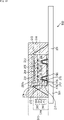
- FIG. It is a figure which shows an example of the semiconductor device provided with general sealing resin.
- FIG. 2 is an enlarged view of the rectangle in FIG. 1;
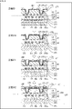
- 2A to 2C are diagrams for explaining a method for manufacturing the semiconductor device of FIG. 1;
- FIG. 2A to 2C are diagrams for explaining a method for manufacturing the semiconductor device of FIG. 1;
- FIG. 2A to 2C are diagrams for explaining a method for manufacturing the semiconductor device of FIG. 1;
- FIG. 2A to 2C are diagrams for explaining a method for manufacturing the semiconductor device of FIG. 1;
- FIG. 2A to 2C are diagrams for explaining a method for manufacturing the semiconductor device of FIG. 1;
- FIG. 2A to 2C are diagrams for explaining a method for manufacturing the semiconductor device of FIG. 1;
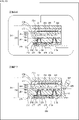
- FIG. It is a figure which shows the 1st example of the package structure of 2nd Embodiment of the semiconductor device to which this technique is applied.
- 1 is a block diagram showing a configuration example of an imaging device as an electronic device to which technology of the present disclosure is applied;
- FIG. It is a figure which shows the usage example which uses a semiconductor chip.
- 1 is a diagram showing an example of a schematic configuration of an endoscopic surgery system;
- FIG. 3 is a block diagram showing an example of functional configurations of a camera head and a CCU;
- FIG. 1 is a block diagram showing an example of a schematic configuration of a vehicle control system;
- FIG. 4 is an explanatory diagram showing an example of installation positions of an outside information detection unit and an imaging unit;
- the definitions of directions such as up and down in the following description are merely definitions for convenience of description, and do not limit the technical idea of the present disclosure. For example, if an object is observed after being rotated by 90°, the upper and lower sides are converted to the left and right when read, and if the object is observed after being rotated by 180°, the upper and lower sides are reversed and read.
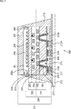
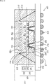
- FIG. 1 is a diagram showing an example of a package structure of a first embodiment of a semiconductor device to which the present technology is applied.
- a semiconductor device 200 in FIG. 1 is configured by mounting a semiconductor chip 211 on a substrate 212 .
- conductors 212a and the like are formed at predetermined positions on the surface of the substrate 212, and photosensitive solder resists 212b are formed on other regions.
- the semiconductor device 200 is configured by mounting the solder balls 279 formed on the lower side of the semiconductor chip 211 on the conductors 212a.
- An underfill material 213 is filled from the periphery of the semiconductor chip 211 between the semiconductor chip 211 and the substrate 212 . That is, an underfill material 213 is formed on the substrate 212 so as to cover the bottom and side surfaces of the semiconductor chip 211 .
- the semiconductor chip 211 is a cavityless CSP (chip size package) in which a transparent protective substrate 232 is formed on a CMOS image sensor 230 as a solid-state imaging device with a seal resin 231 interposed therebetween.
- the seal resin 231 is formed on the upper side of the CMOS image sensor 230 (the side on which light is incident).
- the protective substrate 232 is, for example, a glass substrate, and is bonded to the CMOS image sensor 230 via the seal resin 231 . Details of the seal resin 231 will be described later, but the seal resin 231 includes a base material and a reinforcing material having a higher Young's modulus or breaking strength than the base material.
- the semiconductor chip 211 is a cavityless CSP with no space in which the sealing resin 231 is filled between the CMOS image sensor 230 and the protective substrate 232, it is possible to reduce the height and size of the semiconductor chip. can be done.
- the CMOS image sensor 230 is a stacked back-illuminated CMOS image sensor. Specifically, the CMOS image sensor 230 is configured by stacking an upper substrate 242 on a lower substrate 241 .
- the lower substrate 241 is configured by forming a wiring layer 252 on a supporting substrate 251 such as a silicon substrate.
- Through holes 271 are formed through the support substrate 251 in regions corresponding to the connection pads 252 a of the wiring layer 252 of the support substrate 251 .
- a connection conductor 274 is embedded in the inner wall of the through hole 271 via an insulating film 272 and a barrier/seed layer 273 to form a through silicon via (TSV) 275 .
- a connection conductor 274 of the through silicon electrode 275 is connected to a rewiring 278 formed on the lower surface side of the support substrate 251 via an insulating film 276 and a barrier/seed layer 277 .
- a solder ball 279 is formed at a predetermined position of the rewiring 278 .
- the CMOS image sensor 230 and the substrate 212 are electrically connected. That is, the semiconductor chip 211 is a BGA (Ball Grid Array) package.
- a photosensitive solder resist 280 is formed on the lower surface side of the support substrate 251 so as to cover the insulating film 276 and the rewiring 278 except for the regions where the solder balls 279 are formed.
- logic F circuits such as a control circuit for controlling pixels (not shown) that perform photoelectric conversion formed on the upper substrate 242 and signal processing circuits for processing pixel signals output from the pixels are formed. It is
- the upper substrate 242 is configured by forming a wiring layer 254 on the lower side of the silicon substrate 253 .
- a plurality of photodiodes are formed at predetermined intervals on the surface of the silicon substrate 253 as a photoelectric conversion portion of each pixel.
- a protective film made of SiO 2 is actually formed on the silicon substrate 253 and the photodiode.
- a light-shielding film for preventing light from leaking into adjacent pixels is formed between adjacent photodiodes on the protective film.
- a planarizing film is formed on the protective film and the light shielding film to planarize the region where the color filter 255, which will be described later, is to be formed. Details of this structure are described, for example, in International Publication No. 2014/148276.
- a protective film, a light-shielding film, a planarizing film, and the like are formed on the silicon substrate 253, and hereinafter these are collectively referred to as the silicon substrate 253 as appropriate.
- a color filter 255 is formed on (the planarization film of) the silicon substrate 253 .
- a color filter 255 is provided for each pixel, and the arrangement of colors of the color filter 255 of each pixel is, for example, a Bayer arrangement.
- an on-chip lens (microlens) 256 is formed to collect light on the photodiode of each pixel and improve the sensitivity of the photodiode.
- the on-chip lens 256 is made of an inorganic material such as SiN, SiO, SiOxNy (where x and y are values greater than 0 and less than or equal to 1).
- the semiconductor chip 211 is a cavityless CSP, and the sealing resin 231 exists above the on-chip lens 256 instead of the space. Therefore, if the refractive index of the on-chip lens 256 is higher than the refractive index of the seal resin 231, the light condensing property of the on-chip lens 256 is improved. Therefore, as the material of the on-chip lens 256, it is desirable to use SiN, which has a high refractive index, among SiN, SiO, SiOxNy, and the like.
- the wiring layer 254 forms a pixel circuit. By bonding the wiring layer 254 to the wiring layer 252 , the upper substrate 242 is laminated on the lower substrate 241 .
- FIG. 2 is a diagram showing the circuit configuration of the CMOS image sensor 230 of FIG. 1. As shown in FIG. 1
- the CMOS image sensor 230 includes a pixel array section 291, a control circuit including a vertical driver 292, a column processor 293, a horizontal driver 294, a system controller 295, and the like.
- CMOS image sensor 230 also includes logic circuits such as signal processor 298 and data storage 299 .
- pixels (not shown) having photodiodes or the like for performing photoelectric conversion on received light and accumulating electric charges according to the amount of received light are arranged in the row direction (horizontal direction) and column direction (vertical direction). direction), that is, in a matrix.
- pixel drive lines 296 are wired along the row direction for each row of pixels, and vertical signal lines 297 are wired along the column direction for each column of pixels.
- the pixel drive line 296 transmits a drive signal for driving when reading a signal from a pixel.
- the pixel drive line 296 is shown as one wiring, but it is not limited to one.
- One end of the pixel drive line 296 is connected to an output terminal corresponding to each row of the vertical drive section 292 .
- the vertical driving section 292 is configured by a shift register, an address decoder, and the like, and drives each pixel of the pixel array section 291 simultaneously or in units of rows. Although the specific configuration of the vertical drive unit 292 is omitted from the drawing, it generally has two scanning systems, a readout scanning system and a discharge scanning system.
- the readout scanning system sequentially selectively scans the pixels of the pixel array section 291 row by row in order to read out signals from the pixels.
- a pixel signal which is a signal read out from a pixel, is an analog signal.
- the sweep-scanning system performs sweep-scanning ahead of the read-out scanning by the shutter speed for the read-out rows to be read-scanned by the read-out scanning system. This sweeping scan sweeps out unnecessary charges from the photoelectric conversion units of the pixels in the readout row, resets the photoelectric conversion units, and performs an electronic shutter operation in which charge accumulation is started.
- the pixel signal read out by the readout operation by the readout scanning system corresponds to the amount of light received after the immediately preceding readout operation or the electronic shutter operation.
- a period from the readout timing of the previous readout operation or the sweep timing of the electronic shutter operation to the readout timing of the current readout operation is the charge accumulation period (exposure period) in the pixel.
- a pixel signal read from each pixel in the readout row is input to the column processing unit 293 through each vertical signal line 297 for each column of pixels.
- the column processing unit 293 includes a signal processing circuit for each pixel column of the pixel array unit 291 .
- Each signal processing circuit of the column processing unit 293 performs predetermined signal processing on pixel signals input from the pixels of the corresponding column through the vertical signal line 297, and temporarily holds the pixel signals after the signal processing. .
- each signal processing circuit of the column processing unit 293 performs noise removal processing such as CDS (Correlated Double Sampling) processing as predetermined signal processing.
- This CDS processing removes pixel-specific fixed pattern noise such as reset noise and variations in the threshold value of amplification transistors in pixels.
- the column processing unit 293 also performs A/D (Analog/Digital) conversion processing as predetermined signal processing to convert analog pixel signals into digital signals.
- the horizontal driving section 294 is composed of a shift register, an address decoder, etc., and selects each signal processing circuit of the column processing section 293 in order. Due to the selective scanning by the horizontal driving section 294, the signal processing is performed in each signal processing circuit of the column processing section 293, and the held pixel signals are sequentially output.
- the system control unit 295 is configured by a timing generator that generates various timing signals.
- the system control section 295 controls the vertical driving section 292, the column processing section 293, the horizontal driving section 294, etc. based on various timings generated by this timing generator.
- the signal processing unit 298 has at least an arithmetic processing function, and performs various signal processing such as arithmetic processing on pixel signals, which are digital signals output from the column processing unit 293 .
- the data storage unit 299 temporarily stores data required for signal processing in the signal processing unit 298 .
- FIG. 3 is a diagram showing an example of a semiconductor device provided with a general sealing resin that does not contain a reinforcing material instead of the sealing resin 231 in the semiconductor device 200 of FIG.
- FIG. 3 parts corresponding to those in FIG. 1 are denoted by the same reference numerals, and detailed description of those parts is omitted.
- the semiconductor device 300 is different from the semiconductor device 200 of FIG. 1 in that instead of the sealing resin 231, a general sealing resin 301 using an acrylic polymer containing no reinforcing material is provided. ing.
- cohesive failure occurs in the seal resin 301 in contact with the underfill material 213 due to curing shrinkage stress when the underfill material 213 is thermally cured, and cracks 302 may occur.
- cohesive failure occurs in the seal resin 301 in contact with the underfill material 213 due to curing shrinkage stress when the underfill material 213 is thermally cured, and cracks 302 may occur.
- the whitening of the sealing resin 301 due to the cracks 302 reaches the periphery of the on-chip lens 256, light is diffusely reflected at the whitened portion, degrading the image quality of the captured image.
- the light reflected by the on-chip lens 256 and the surface of the silicon substrate 253 is totally reflected by the upper surface (surface) of the protective substrate 232, and re-enters the light receiving region of the silicon substrate 253 where the photodiodes are formed.
- a periodic diffraction ghost or diffraction flare may occur in the captured image.
- the seal resin 301 and the protective substrate 232 have substantially the same refractive index, the light reflected by the surface of the on-chip lens 256 and silicon substrate 253 travels straight to the surface of the protective substrate 232 away from this surface. Therefore, due to the light totally reflected by the protective substrate 232 , a strong diffraction ghost may be generated at a position distant from the reflection position on the surface of the on-chip lens 256 or silicon substrate 253 .
- Such diffraction ghosts and diffraction flares are unintended reflections of light, that is, noise, and are undesirable.
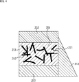
- FIG. 4 is an enlarged view of rectangle A in FIG.
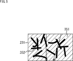
- the sealing resin 231 has a composite structure including randomly dispersed reinforcing materials 352 having a higher Young's modulus or breaking strength than the base material 351 .
- the sealing resin 231 contains the reinforcing material 352 , the sealing resin 231 can be reinforced more than the sealing resin 301 . Therefore, cohesive failure of the seal resin 231 due to curing shrinkage stress when the underfill material 213 is thermally cured can be suppressed. As a result, occurrence of whitening of the seal resin 231 is reduced, and deterioration of image quality of the captured image due to this whitening is suppressed.
- the cracks 371 can be stopped at the interface of the reinforcing material 352 . Therefore, it is possible to prevent the crack 371 from growing around the on-chip lens 256, that is, on the light receiving area. As a result, the whitening of the sealing resin 231 can be prevented from adversely affecting the image quality of the captured image.
- the semiconductor chip 211 is protected by the underfill material 213 to ensure long-term reliability after the semiconductor chip 211 is mounted on the substrate 212, while the whitening of the seal resin 231 prevents deterioration of image quality of captured images. can be suppressed.
- the seal resin 231 is configured, for example, so that the average transmittance in the visible light wavelength range (for example, 400 nm to 700 nm) is 98.5% or higher.
- the base material 351 is an acrylic sealing resin having a refractive index lower than that of the on-chip lens 256 and substantially equal to that of the protective substrate 232 .
- the protective substrate 232 is a glass substrate with a refractive index of 1.51
- the base material 351 is, for example, acrylic resin with a refractive index of 1.5.
- the seal resin 231 since the refractive index of the base material 351 is lower than that of the on-chip lens 256, the light condensing property of the on-chip lens 256 can be improved. Moreover, since the protective substrate 232 and the base material 351 have substantially the same refractive index, the influence of the base material 351 on the light incident on the light receiving region through the protective substrate 232 can be suppressed.
- the reinforcing material 352 is a fibrous material that transmits visible light.
- examples of such materials include glass fibers, cellulose nanofibers, and organic fibers such as nanoparticle aggregates having a particle size of 100 nm or less.
- Cellulose nanofibers are transparent cellulose fibers thinned to the nano level, which are formed by hydrolyzing and pulverizing wood or the like. Cellulose nanofibers, for example, are five times stronger than steel.
- the cross-sectional diameter of the short side of the reinforcing material 352 is shorter than the wavelength of visible light, and the cross-sectional diameter of the long side is three times or more the cross-sectional diameter of the short side, that is, the aspect ratio is 3 or more. Thereby, the influence of the reinforcing material 352 on the light incident on the light receiving region through the protective substrate 232 can be suppressed.
- the refractive index of the reinforcing material 352 is approximately equal to the refractive index of the base material 351. Specifically, it is desirable that the difference in refractive index between the reinforcing material 352 and the base material 351 is, for example, 0.03 or more and 0.06 or less. If the difference in refractive index between the reinforcing material 352 and the base material 351 is 0.06 or less, the effect of the reinforcing material 352 on the light incident on the light receiving region through the protective substrate 232 can be suppressed. As a result, deterioration of image quality due to the reinforcing material 352 can be suppressed.
- the difference in refractive index between the reinforcing material 352 and the base material 351 is 0.03 or more, as shown in FIG. change direction.
- the light is reflected by the light receiving area and the on-chip lens 256, enters the protective substrate 232 through the sealing resin 231, is totally reflected by the upper surface of the protective substrate 232, and enters the light receiving area again through the sealing resin 231 and the like. It is possible to suppress the occurrence of the phase shift of the light to be emitted. As a result, it is possible to reduce the occurrence of diffraction ghosts (brightness and darkness of light) and diffraction flare in captured images due to this phase shift. Thereby, the image quality of the captured image can be improved.
- the reinforcing material 352 is dispersed in the base material 351 at a ratio of 2-50 wt%. As a result, it is possible to suppress the deterioration of the resolution of the captured image due to the dense concentration of the reinforcing material 352 .
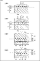
- ⁇ Method for manufacturing a semiconductor device> 6 to 10 are diagrams for explaining the manufacturing method of the semiconductor device 200 of FIG.
- step S1 of FIG. 6 the CMOS image sensor 230 without the through silicon via 275, the insulating film 276, the barrier/seed layer 277, the rewiring 278, the solder ball 279, and the photosensitive solder resist 280 is formed. Specifically, an upper substrate 242 on which a color filter 255 and an on-chip lens 256 are formed is laminated on a lower substrate 241 on which nothing is formed on a support substrate 251 yet.
- step S2 the CMOS image sensor 230 and the protection substrate 232, which are formed in step S1 and are not formed with the through-silicon electrodes 275 and the like, are connected in a cavityless structure.
- the sealing resin 231 is applied or laminated with a thickness of 5 to 100 ⁇ m on the on-chip lens 256 of the CMOS image sensor 230 where the silicon through electrode 275 and the like formed in step S1 are not formed. It is formed by Then, through this sealing resin 231, the protective substrate 232 is adhered to the CMOS image sensor 230 in which the silicon through electrode 275 and the like are not formed.
- step S3 the CMOS image sensor 230 and the protective substrate 232, which were connected in the cavityless structure in step S2, are turned upside down.
- step S4 the support substrate 251 is thinned to about 100 ⁇ m, for example, using a back grinding technique.
- step S5 of FIG. 7 resist patterning is performed to apply a resist 401 to regions other than regions corresponding to the connection pads 252a on the support substrate 251 in order to extract electrodes from the back surface of the CMOS image sensor 230.
- the support substrate 251 is penetrated using a dry etching method to form a through hole 271 .
- a SiO2 film, a SiN film, or the like is formed as an insulating film (isolation film) on the entire surface of the support substrate 251 including the through holes 271 by plasma CVD (Chemical Vapor Deposition), for example. Then, the insulating film on the bottom surface of the through-hole 271 is removed using an etch-back method to expose the connection pad 252a formed in the region of the wiring layer 252 closest to the support substrate 251 . As a result, an insulating film 272 is formed on the through hole 271 and an insulating film 276 is formed on the region of the support substrate 251 other than the through hole 271 .
- plasma CVD Chemical Vapor Deposition
- a barrier/seed layer 273 is formed on the bottom surface of the through hole 271 and the insulating film 272, and a barrier/seed layer 277 is formed on the insulating film 276 using a sputtering method.
- the barrier/seed layer 273 and the barrier/seed layer 277 are composed of a barrier metal film for preventing the diffusion of copper (Cu) plated in step S8, which will be described later, and a Cu seed layer that serves as an electrode during the plating. be.
- titanium (Ti) is used as the material of the barrier metal film, but the material of the barrier metal film may be titanium, tungsten (W), titanium (Ti), or tungsten (W).
- a nitride film, or an alloy of titanium (Ti) or tungsten (W) can also be used.
- step S8 resist patterning is performed to apply a resist 403 to a region on the barrier/seed layer 277 other than the region where the rewiring 278 is formed.
- step S9 of FIG. 8 areas where the resist 403 is not applied are plated with copper (Cu) by electroplating.
- the connecting conductor 274 is embedded in the inner wall of the through-hole 271 via the insulating film 272 and the barrier/seed layer 273, and as a result, the through-silicon electrode 275 is formed.
- a rewiring 278 that connects with the connection conductor 274 is formed via the insulating film 276 and the barrier/seed layer 277 .
- step S10 the resist 403 is removed.
- a wet etch then removes the barrier/seed layer 277 under the resist 403 .
- step S11 a photosensitive solder resist is applied, exposed, and developed on the through silicon vias 275, the insulating film 276, and the rewiring 278, and the photosensitive solder resist is applied to the regions other than the regions where the solder balls 279 are to be formed. 280 are formed.
- step S12 solder balls 279 are mounted using the ball transfer method in areas where the photosensitive solder resist 280 is not formed in step S11.
- the semiconductor chip 211 is formed as described above.
- steps S1 to S12 may be performed in units of wafers, or may be performed in units of individualized chips.
- a substrate 212 is formed in which conductors 212a are formed at positions where solder balls 279 are mounted on the surface, and photosensitive solder resists 212b are formed in other regions.
- solder 420 is pre-coated onto the conductors 212a of the substrate 212 by solder paste printing.
- step S15 the solder balls 279 of the semiconductor chip 211 are mounted on the conductors 212a via the solder 420.
- step S16 of FIG. 10 the substrate 212 on which the semiconductor chip 211 is mounted is reflowed in a surface mount type reflow furnace provided with a plurality of different temperature zones. Thereby, the semiconductor chip 211 is soldered to the substrate 212 via the solder balls 279 . After that, the solder paste residue (flux residue) remaining between the semiconductor chip 211 and the substrate 212 is removed using a dedicated cleaning liquid.
- the solder flux is a rosin-based flux
- an alcohol-based cleaning liquid is used as the dedicated cleaning liquid.
- the semiconductor chip 211 is secondarily mounted on the substrate 212 .
- an epoxy thermosetting underfill material 425 is filled between the semiconductor chip 211 and the substrate 212 .
- the underfill material 425 is injected between the semiconductor chip 211 and the substrate 212 from around one side of the semiconductor chip 211 using a dispensing nozzle 426 .
- the protruding underfill material 425 creeps up on the side wall of the semiconductor chip 211 to form a fillet.
- the filled underfill material 425 is thermally cured, for example, at 150° C. for 5 minutes.
- the underfill material 213 is formed to cover the bottom and side surfaces of the semiconductor chip 211 .
- the semiconductor chip 211 is mounted on the substrate 212.
- ICs Integrated Circuits
- passive components etc.
- other components other parts are also soldered collectively together with the semiconductor chip 211 .
- conductors are also formed at positions where other components are mounted on the surface of the substrate 212, and the conductors are also pre-coated with solder in step S14.
- step S15 the semiconductor chip 211 is mounted on the conductor 212a via the solder 420, and other components are mounted on conductors other than the conductor 212a via solder.
- step S16 reflow is performed on the substrate 212 on which the semiconductor chip 211 and other components are mounted, and the semiconductor chip 211 and other components are soldered to the substrate 212 all at once.
- the sealing resin 231 that bonds the CMOS image sensor 230 and the protective substrate 232 contains the base material 351 and the reinforcing material 352 having a higher Young's modulus or breaking strength than the base material 351 .
- the strength of the sealing resin 231 can be improved compared to the sealing resin 301 or the like that does not contain the reinforcing material 352 .
- the crack resistance of the seal resin 231 against stress such as curing shrinkage stress generated when the underfill material 213 is thermally cured can be improved.
- the cracks 371 can be stopped at the interface of the reinforcing material 352 . Therefore, it is possible to prevent the crack 371 from growing above the light receiving region.
- the whitening of the seal resin 231 prevents deterioration of image quality of the picked-up image. can be suppressed.
- solder balls 279 are formed, but the solder balls 279 do not have to be formed.
- FIG. 11 is a diagram showing a first example of a package structure of a second embodiment of a semiconductor device to which the present technology is applied.
- the semiconductor chip 211 of FIG. 1 is wire-bonded to the substrate 212 rather than soldered. Specifically, the semiconductor device 500 is mounted by connecting the semiconductor chip 511 to the relay board 512 via the wire 513 .
- the semiconductor chip 511 is provided with a CMOS image sensor 520 instead of the CMOS image sensor 230, the circumference of the sealing resin 231 is smaller than the circumference of the CMOS image sensor 230, and the wire 513 is provided. , and otherwise configured in the same manner as the semiconductor chip 211 .
- the CMOS image sensor 520 differs from the CMOS image sensor 230 in that solder balls 279 are not formed, and is otherwise configured in the same manner as the CMOS image sensor 230 .
- the wire 513 is formed in a region where the seal resin 231 is not formed on the silicon substrate 253 and electrically connects the silicon substrate 253 and the relay substrate 512 .
- the wires 513 are embedded in the resin 514 . That is, a resin 514 is formed on the relay substrate 512 so as to cover the wires 513 on the side surfaces of the semiconductor chip 511 . Solder balls 515 are formed on the lower side of the relay board 512 for mounting on a mounting board (not shown).
- the semiconductor device 500 is a BGA package having an organic package structure in which the semiconductor chip 511 is wire-bonded to the relay substrate 512 using the wires 513 and the wires 513 are embedded with the resin 514 .
- the sealing resin 231 contains the reinforcing material 352
- the crack resistance of the sealing resin 231 against stress such as curing shrinkage stress generated when the resin 514 is thermally cured is high.
- the crack 371 occurs due to cohesive failure, it is possible to prevent the crack 371 from propagating above the light receiving region.
- the semiconductor chip 511 is protected by the resin 514 to ensure long-term reliability after the semiconductor chip 511 is mounted on the relay substrate 512 , while preventing image quality deterioration of the picked-up image due to whitening of the sealing resin 231 . can be suppressed.
- FIG. 12 is a diagram showing a second example of the package structure of the second embodiment of the semiconductor device to which the present technology is applied.
- the parts corresponding to those of the semiconductor device 500 of FIG. 11 are denoted by the same reference numerals. Therefore, the description of that portion is omitted as appropriate, and the description focuses on the portions different from the semiconductor device 500 of FIG.
- the semiconductor device 550 of FIG. 12 differs from the semiconductor device 500 in that a mounting substrate 551 is provided instead of the relay substrate 512 and that solder balls 515 are not formed. It is
- the semiconductor chip 511 is wire-bonded to the mounting board 551 using the wires 513 , and the semiconductor chip 511 is directly mounted on the mounting board 551 .
- the sealing resin 231 contains the reinforcing material 352 as in the semiconductor device 500 . Accordingly, it is possible to protect the semiconductor chip 511 with the resin 514 and ensure long-term reliability after the semiconductor chip 511 is mounted on the mounting board 551 , while suppressing deterioration of image quality of the picked-up image due to whitening of the sealing resin 231 .
- CMOS image sensor 230 or 520 is a laminated backside illumination CMOS image sensor, it may be a frontside or backside illumination CMOS image sensor.
- control circuit and the logic circuit are formed on the lower substrate 241, and the pixel region is formed on the upper substrate 242.
- a pixel region and a control circuit may be formed in 242 .
- the above-described semiconductor chip 211 or 511 can be applied to various electronic devices such as imaging devices such as digital still cameras and digital video cameras, mobile phones with imaging functions, and other devices with imaging functions. can be done.
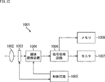
- FIG. 13 is a block diagram showing a configuration example of an imaging device as an electronic device to which this technology is applied.
- An imaging apparatus 1001 shown in FIG. 13 includes an optical system 1002, a shutter device 1003, a solid-state imaging device 1004, a driving circuit 1005, a signal processing circuit 1006, a monitor 1007, and a memory 1008, and captures still images and moving images. Imaging is possible.
- the optical system 1002 includes one or more lenses, guides light (incident light) from a subject to the solid-state imaging device 1004, and forms an image on the light-receiving surface of the solid-state imaging device 1004.
- the shutter device 1003 is arranged between the optical system 1002 and the solid-state imaging device 1004, and controls the light irradiation period and the light shielding period for the solid-state imaging device 1004 according to the control of the drive circuit 1005.
- the solid-state imaging device 1004 is composed of the semiconductor chip 211 or 511 described above.
- the solid-state imaging device 1004 accumulates signal charges for a certain period of time according to the light imaged on the light receiving surface via the optical system 1002 and the shutter device 1003 .
- the signal charges accumulated in the solid-state imaging device 1004 are transferred according to the drive signal (timing signal) supplied from the drive circuit 1005 .
- a driving circuit 1005 drives the solid-state imaging device 1004 and the shutter device 1003 by outputting drive signals for controlling the transfer operation of the solid-state imaging device 1004 and the shutter operation of the shutter device 1003 .
- a signal processing circuit 1006 performs various signal processing on the signal charges output from the solid-state imaging device 1004 .
- An image (image data) obtained by the signal processing performed by the signal processing circuit 1006 is supplied to the monitor 1007 to be displayed, or supplied to the memory 1008 to be stored (recorded).
- the imaging device 1001 configured in this way, by applying the semiconductor chip 211 (511) as the solid-state imaging device 1004, long-term reliability after mounting on the substrate 212 (relay substrate 512, mounting substrate 551) can be achieved. while ensuring the quality of the captured image.
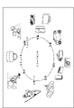
- FIG. 14 is a diagram showing a usage example using the semiconductor chip 211 or 511 described above.
- the semiconductor chip 211 or 511 described above can be used in various cases for sensing light such as visible light, infrared light, ultraviolet light, and X-rays, for example, as follows.
- ⁇ Devices that capture images for viewing purposes, such as digital cameras and mobile devices with camera functions.
- Devices used for transportation such as in-vehicle sensors that capture images behind, around, and inside the vehicle, surveillance cameras that monitor running vehicles and roads, and ranging sensors that measure the distance between vehicles.
- Devices used in home appliances such as TVs, refrigerators, air conditioners, etc., to take pictures and operate devices according to gestures ⁇ Endoscopes, devices that perform angiography by receiving infrared light, etc.
- Equipment used for medical and healthcare purposes such as surveillance cameras for crime prevention and cameras for personal authentication
- microscopes used for beauty such as microscopes used for beauty
- Sports such as action cameras and wearable cameras for use in sports ⁇ Cameras, etc. for monitoring the condition of fields and crops , agricultural equipment
- Example of application to an endoscopic surgery system The technology (the present technology) according to the present disclosure can be applied to various products.
- the technology according to the present disclosure may be applied to an endoscopic surgery system.
- FIG. 15 is a diagram showing an example of a schematic configuration of an endoscopic surgery system to which the technology according to the present disclosure (this technology) can be applied.
- FIG. 15 illustrates a state in which an operator (doctor) 11131 is performing surgery on a patient 11132 on a patient bed 11133 using an endoscopic surgery system 11000 .
- an endoscopic surgery system 11000 includes an endoscope 11100, other surgical instruments 11110 such as a pneumoperitoneum tube 11111 and an energy treatment instrument 11112, and a support arm device 11120 for supporting the endoscope 11100. , and a cart 11200 loaded with various devices for endoscopic surgery.
- An endoscope 11100 is composed of a lens barrel 11101 whose distal end is inserted into the body cavity of a patient 11132 and a camera head 11102 connected to the proximal end of the lens barrel 11101 .
- an endoscope 11100 configured as a so-called rigid scope having a rigid lens barrel 11101 is illustrated, but the endoscope 11100 may be configured as a so-called flexible scope having a flexible lens barrel. good.
- the tip of the lens barrel 11101 is provided with an opening into which the objective lens is fitted.
- a light source device 11203 is connected to the endoscope 11100, and light generated by the light source device 11203 is guided to the tip of the lens barrel 11101 by a light guide extending inside the lens barrel 11101, where it reaches the objective. Through the lens, the light is irradiated toward the observation object inside the body cavity of the patient 11132 .
- the endoscope 11100 may be a straight scope, a perspective scope, or a side scope.
- An optical system and an imaging element are provided inside the camera head 11102, and the reflected light (observation light) from the observation target is focused on the imaging element by the optical system.
- the imaging device photoelectrically converts the observation light to generate an electrical signal corresponding to the observation light, that is, an image signal corresponding to the observation image.
- the image signal is transmitted to a camera control unit (CCU: Camera Control Unit) 11201 as RAW data.
- CCU Camera Control Unit
- the CCU 11201 is composed of a CPU (Central Processing Unit), a GPU (Graphics Processing Unit), etc., and controls the operations of the endoscope 11100 and the display device 11202 in an integrated manner. Further, the CCU 11201 receives an image signal from the camera head 11102 and performs various image processing such as development processing (demosaicing) for displaying an image based on the image signal.
- CPU Central Processing Unit
- GPU Graphics Processing Unit
- the display device 11202 displays an image based on an image signal subjected to image processing by the CCU 11201 under the control of the CCU 11201 .
- the light source device 11203 is composed of a light source such as an LED (Light Emitting Diode), for example, and supplies the endoscope 11100 with irradiation light for photographing a surgical site or the like.
- a light source such as an LED (Light Emitting Diode), for example, and supplies the endoscope 11100 with irradiation light for photographing a surgical site or the like.
- the input device 11204 is an input interface for the endoscopic surgery system 11000.
- the user can input various information and instructions to the endoscopic surgery system 11000 via the input device 11204 .
- the user inputs an instruction or the like to change the imaging conditions (type of irradiation light, magnification, focal length, etc.) by the endoscope 11100 .
- the treatment instrument control device 11205 controls driving of the energy treatment instrument 11112 for tissue cauterization, incision, blood vessel sealing, or the like.
- the pneumoperitoneum device 11206 inflates the body cavity of the patient 11132 for the purpose of securing the visual field of the endoscope 11100 and securing the operator's working space, and injects gas into the body cavity through the pneumoperitoneum tube 11111. send in.
- the recorder 11207 is a device capable of recording various types of information regarding surgery.
- the printer 11208 is a device capable of printing various types of information regarding surgery in various formats such as text, images, and graphs.
- the light source device 11203 that supplies the endoscope 11100 with irradiation light for photographing the surgical site can be composed of, for example, a white light source composed of an LED, a laser light source, or a combination thereof.
- a white light source is configured by a combination of RGB laser light sources
- the output intensity and output timing of each color (each wavelength) can be controlled with high accuracy. It can be carried out.
- the observation target is irradiated with laser light from each of the RGB laser light sources in a time-division manner, and by controlling the drive of the imaging element of the camera head 11102 in synchronization with the irradiation timing, each of RGB can be handled. It is also possible to pick up images by time division. According to this method, a color image can be obtained without providing a color filter in the imaging device.
- the driving of the light source device 11203 may be controlled so as to change the intensity of the output light every predetermined time.
- the drive of the imaging device of the camera head 11102 in synchronism with the timing of the change in the intensity of the light to obtain an image in a time-division manner and synthesizing the images, a high dynamic A range of images can be generated.
- the light source device 11203 may be configured to be able to supply light in a predetermined wavelength band corresponding to special light observation.
- special light observation for example, the wavelength dependence of light absorption in body tissues is used to irradiate a narrower band of light than the irradiation light (i.e., white light) used during normal observation, thereby observing the mucosal surface layer.
- narrow band imaging in which a predetermined tissue such as a blood vessel is imaged with high contrast, is performed.
- fluorescence observation may be performed in which an image is obtained from fluorescence generated by irradiation with excitation light.
- the body tissue is irradiated with excitation light and the fluorescence from the body tissue is observed (autofluorescence observation), or a reagent such as indocyanine green (ICG) is locally injected into the body tissue and the body tissue is A fluorescence image can be obtained by irradiating excitation light corresponding to the fluorescence wavelength of the reagent.
- the light source device 11203 can be configured to be able to supply narrowband light and/or excitation light corresponding to such special light observation.
- FIG. 16 is a block diagram showing an example of functional configurations of the camera head 11102 and CCU 11201 shown in FIG.
- the camera head 11102 has a lens unit 11401, an imaging section 11402, a drive section 11403, a communication section 11404, and a camera head control section 11405.
- the CCU 11201 has a communication section 11411 , an image processing section 11412 and a control section 11413 .
- the camera head 11102 and the CCU 11201 are communicably connected to each other via a transmission cable 11400 .
- a lens unit 11401 is an optical system provided at a connection with the lens barrel 11101 . Observation light captured from the tip of the lens barrel 11101 is guided to the camera head 11102 and enters the lens unit 11401 .
- a lens unit 11401 is configured by combining a plurality of lenses including a zoom lens and a focus lens.
- the imaging unit 11402 is composed of an imaging element.
- the imaging device constituting the imaging unit 11402 may be one (so-called single-plate type) or plural (so-called multi-plate type).
- image signals corresponding to RGB may be generated by each image pickup element, and a color image may be obtained by synthesizing the image signals.
- the imaging unit 11402 may be configured to have a pair of imaging elements for respectively acquiring right-eye and left-eye image signals corresponding to 3D (Dimensional) display.
- the 3D display enables the operator 11131 to more accurately grasp the depth of the living tissue in the surgical site.
- a plurality of systems of lens units 11401 may be provided corresponding to each imaging element.
- the imaging unit 11402 does not necessarily have to be provided in the camera head 11102 .
- the imaging unit 11402 may be provided inside the lens barrel 11101 immediately after the objective lens.
- the drive unit 11403 is configured by an actuator, and moves the zoom lens and focus lens of the lens unit 11401 by a predetermined distance along the optical axis under control from the camera head control unit 11405 . Thereby, the magnification and focus of the image captured by the imaging unit 11402 can be appropriately adjusted.
- the communication unit 11404 is composed of a communication device for transmitting and receiving various information to and from the CCU 11201.
- the communication unit 11404 transmits the image signal obtained from the imaging unit 11402 as RAW data to the CCU 11201 via the transmission cable 11400 .
- the communication unit 11404 receives a control signal for controlling driving of the camera head 11102 from the CCU 11201 and supplies it to the camera head control unit 11405 .
- the control signal includes, for example, information to specify the frame rate of the captured image, information to specify the exposure value at the time of imaging, and/or information to specify the magnification and focus of the captured image. Contains information about conditions.
- the imaging conditions such as the frame rate, exposure value, magnification, and focus may be appropriately designated by the user, or may be automatically set by the control unit 11413 of the CCU 11201 based on the acquired image signal. good.
- the endoscope 11100 is equipped with so-called AE (Auto Exposure) function, AF (Auto Focus) function, and AWB (Auto White Balance) function.
- the camera head control unit 11405 controls driving of the camera head 11102 based on the control signal from the CCU 11201 received via the communication unit 11404.
- the communication unit 11411 is composed of a communication device for transmitting and receiving various information to and from the camera head 11102 .
- the communication unit 11411 receives image signals transmitted from the camera head 11102 via the transmission cable 11400 .
- the communication unit 11411 transmits a control signal for controlling driving of the camera head 11102 to the camera head 11102 .
- Image signals and control signals can be transmitted by electric communication, optical communication, or the like.
- the image processing unit 11412 performs various types of image processing on the image signal, which is RAW data transmitted from the camera head 11102 .
- the control unit 11413 performs various controls related to imaging of the surgical site and the like by the endoscope 11100 and display of the captured image obtained by imaging the surgical site and the like. For example, the control unit 11413 generates control signals for controlling driving of the camera head 11102 .
- control unit 11413 causes the display device 11202 to display a captured image showing the surgical site and the like based on the image signal that has undergone image processing by the image processing unit 11412 .
- the control unit 11413 may recognize various objects in the captured image using various image recognition techniques. For example, the control unit 11413 detects the shape, color, and the like of the edges of objects included in the captured image, thereby detecting surgical instruments such as forceps, specific body parts, bleeding, mist during use of the energy treatment instrument 11112, and the like. can recognize.
- the control unit 11413 may use the recognition result to display various types of surgical assistance information superimposed on the image of the surgical site. By superimposing and presenting the surgery support information to the operator 11131, the burden on the operator 11131 can be reduced and the operator 11131 can proceed with the surgery reliably.
- a transmission cable 11400 connecting the camera head 11102 and the CCU 11201 is an electrical signal cable compatible with electrical signal communication, an optical fiber compatible with optical communication, or a composite cable of these.
- wired communication is performed using the transmission cable 11400, but communication between the camera head 11102 and the CCU 11201 may be performed wirelessly.
- the technology according to the present disclosure can be applied to the imaging unit 11402 among the configurations described above.
- the semiconductor chip 211 or 511 can be applied to the imaging unit 11402 .
- the technology according to the present disclosure may also be applied to, for example, a microsurgery system.
- the technology (the present technology) according to the present disclosure can be applied to various products.
- the technology according to the present disclosure can be realized as a device mounted on any type of moving body such as automobiles, electric vehicles, hybrid electric vehicles, motorcycles, bicycles, personal mobility, airplanes, drones, ships, and robots. may
- FIG. 17 is a block diagram showing a schematic configuration example of a vehicle control system, which is an example of a mobile control system to which the technology according to the present disclosure can be applied.
- a vehicle control system 12000 includes a plurality of electronic control units connected via a communication network 12001.
- the vehicle control system 12000 includes a drive system control unit 12010, a body system control unit 12020, an outside information detection unit 12030, an inside information detection unit 12040, and an integrated control unit 12050.
- a microcomputer 12051, an audio/image output unit 12052, and an in-vehicle network I/F (interface) 12053 are illustrated.
- the drive system control unit 12010 controls the operation of devices related to the drive system of the vehicle according to various programs.
- the driving system control unit 12010 includes a driving force generator for generating driving force of the vehicle such as an internal combustion engine or a driving motor, a driving force transmission mechanism for transmitting the driving force to the wheels, and a steering angle of the vehicle. It functions as a control device such as a steering mechanism to adjust and a brake device to generate braking force of the vehicle.
- the body system control unit 12020 controls the operation of various devices equipped on the vehicle body according to various programs.
- the body system control unit 12020 functions as a keyless entry system, a smart key system, a power window device, or a control device for various lamps such as headlamps, back lamps, brake lamps, winkers or fog lamps.
- the body system control unit 12020 can receive radio waves transmitted from a portable device that substitutes for a key or signals from various switches.
- the body system control unit 12020 receives the input of these radio waves or signals and controls the door lock device, power window device, lamps, etc. of the vehicle.
- the vehicle exterior information detection unit 12030 detects information outside the vehicle in which the vehicle control system 12000 is installed.
- the vehicle exterior information detection unit 12030 is connected with an imaging section 12031 .
- the vehicle exterior information detection unit 12030 causes the imaging unit 12031 to capture an image of the exterior of the vehicle, and receives the captured image.
- the vehicle exterior information detection unit 12030 may perform object detection processing or distance detection processing such as people, vehicles, obstacles, signs, or characters on the road surface based on the received image.
- the imaging unit 12031 is an optical sensor that receives light and outputs an electrical signal according to the amount of received light.
- the imaging unit 12031 can output the electric signal as an image, and can also output it as distance measurement information.
- the light received by the imaging unit 12031 may be visible light or non-visible light such as infrared rays.
- the in-vehicle information detection unit 12040 detects in-vehicle information.
- the in-vehicle information detection unit 12040 is connected to, for example, a driver state detection section 12041 that detects the state of the driver.
- the driver state detection unit 12041 includes, for example, a camera that captures an image of the driver, and the in-vehicle information detection unit 12040 detects the degree of fatigue or concentration of the driver based on the detection information input from the driver state detection unit 12041. It may be calculated, or it may be determined whether the driver is dozing off.
- the microcomputer 12051 calculates control target values for the driving force generator, the steering mechanism, or the braking device based on the information inside and outside the vehicle acquired by the vehicle exterior information detection unit 12030 or the vehicle interior information detection unit 12040, and controls the drive system control unit.
- a control command can be output to 12010 .
- the microcomputer 12051 realizes the functions of ADAS (Advanced Driver Assistance System) including collision avoidance or shock mitigation, follow-up driving based on inter-vehicle distance, vehicle speed maintenance driving, vehicle collision warning, or vehicle lane deviation warning. Cooperative control can be performed for the purpose of ADAS (Advanced Driver Assistance System) including collision avoidance or shock mitigation, follow-up driving based on inter-vehicle distance, vehicle speed maintenance driving, vehicle collision warning, or vehicle lane deviation warning. Cooperative control can be performed for the purpose of ADAS (Advanced Driver Assistance System) including collision avoidance or shock mitigation, follow-up driving based on inter-vehicle distance, vehicle speed maintenance driving, vehicle collision warning, or vehicle
- the microcomputer 12051 controls the driving force generator, the steering mechanism, the braking device, etc. based on the information about the vehicle surroundings acquired by the vehicle exterior information detection unit 12030 or the vehicle interior information detection unit 12040, so that the driver's Cooperative control can be performed for the purpose of autonomous driving, etc., in which vehicles autonomously travel without depending on operation.
- the microcomputer 12051 can output a control command to the body system control unit 12020 based on the information outside the vehicle acquired by the information detection unit 12030 outside the vehicle.
- the microcomputer 12051 controls the headlamps according to the position of the preceding vehicle or the oncoming vehicle detected by the vehicle exterior information detection unit 12030, and performs cooperative control aimed at anti-glare such as switching from high beam to low beam. It can be carried out.
- the audio/image output unit 12052 transmits at least one of audio and/or image output signals to an output device capable of visually or audibly notifying the passengers of the vehicle or the outside of the vehicle.
- an audio speaker 12061, a display unit 12062, and an instrument panel 12063 are illustrated as output devices.
- the display unit 12062 may include at least one of an on-board display and a head-up display, for example.
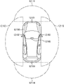
- FIG. 18 is a diagram showing an example of the installation position of the imaging unit 12031.
- the vehicle 12100 has imaging units 12101, 12102, 12103, 12104, and 12105 as the imaging unit 12031.
- the imaging units 12101, 12102, 12103, 12104, and 12105 are provided at positions such as the front nose of the vehicle 12100, the side mirrors, the rear bumper, the back door, and the upper part of the windshield in the vehicle interior, for example.
- An image pickup unit 12101 provided in the front nose and an image pickup unit 12105 provided above the windshield in the passenger compartment mainly acquire images in front of the vehicle 12100 .
- Imaging units 12102 and 12103 provided in the side mirrors mainly acquire side images of the vehicle 12100 .
- An imaging unit 12104 provided in the rear bumper or back door mainly acquires an image behind the vehicle 12100 .
- Forward images acquired by the imaging units 12101 and 12105 are mainly used for detecting preceding vehicles, pedestrians, obstacles, traffic lights, traffic signs, lanes, and the like.
- FIG. 18 shows an example of the imaging range of the imaging units 12101 to 12104.
- the imaging range 12111 indicates the imaging range of the imaging unit 12101 provided in the front nose
- the imaging ranges 12112 and 12113 indicate the imaging ranges of the imaging units 12102 and 12103 provided in the side mirrors, respectively
- the imaging range 12114 The imaging range of an imaging unit 12104 provided on the rear bumper or back door is shown. For example, by superimposing the image data captured by the imaging units 12101 to 12104, a bird's-eye view image of the vehicle 12100 viewed from above can be obtained.
- At least one of the imaging units 12101 to 12104 may have a function of acquiring distance information.
- at least one of the imaging units 12101 to 12104 may be a stereo camera composed of a plurality of imaging elements, or may be an imaging element having pixels for phase difference detection.
- the microcomputer 12051 determines the distance to each three-dimensional object within the imaging ranges 12111 to 12114 and changes in this distance over time (relative velocity with respect to the vehicle 12100). , it is possible to extract, as the preceding vehicle, the closest three-dimensional object on the course of the vehicle 12100, which runs at a predetermined speed (for example, 0 km/h or more) in substantially the same direction as the vehicle 12100. can. Furthermore, the microcomputer 12051 can set the inter-vehicle distance to be secured in advance in front of the preceding vehicle, and perform automatic brake control (including following stop control) and automatic acceleration control (including following start control). In this way, cooperative control can be performed for the purpose of automatic driving in which the vehicle runs autonomously without relying on the operation of the driver.
- automatic brake control including following stop control
- automatic acceleration control including following start control
- the microcomputer 12051 converts three-dimensional object data related to three-dimensional objects to other three-dimensional objects such as motorcycles, ordinary vehicles, large vehicles, pedestrians, and utility poles. It can be classified and extracted and used for automatic avoidance of obstacles. For example, the microcomputer 12051 distinguishes obstacles around the vehicle 12100 into those that are visible to the driver of the vehicle 12100 and those that are difficult to see. Then, the microcomputer 12051 judges the collision risk indicating the degree of danger of collision with each obstacle, and when the collision risk is equal to or higher than the set value and there is a possibility of collision, an audio speaker 12061 and a display unit 12062 are displayed. By outputting an alarm to the driver via the drive system control unit 12010 and performing forced deceleration and avoidance steering via the drive system control unit 12010, driving support for collision avoidance can be performed.
- At least one of the imaging units 12101 to 12104 may be an infrared camera that detects infrared rays.
- the microcomputer 12051 can recognize a pedestrian by determining whether or not the pedestrian exists in the captured images of the imaging units 12101 to 12104 .
- recognition of a pedestrian is performed by, for example, a procedure for extracting feature points in images captured by the imaging units 12101 to 12104 as infrared cameras, and performing pattern matching processing on a series of feature points indicating the outline of an object to determine whether or not the pedestrian is a pedestrian.
- the audio image output unit 12052 outputs a rectangular outline for emphasis to the recognized pedestrian. is superimposed on the display unit 12062 . Also, the audio/image output unit 12052 may control the display unit 12062 to display an icon or the like indicating a pedestrian at a desired position.
- the technology according to the present disclosure can be applied to the imaging unit 12031 and the like among the configurations described above.
- the semiconductor chip 211 or 511 can be applied to the imaging section 12031 .
- Embodiments of the present technology are not limited to the above-described embodiments, and various modifications are possible without departing from the gist of the present technology.
- this technique can take the following configurations.
- (12) (11) The semiconductor chip according to (11), wherein a difference in refractive index between the reinforcing material and the base material is 0.03 or more and 0.06 or less.
- the imaging device includes an on-chip lens, The semiconductor chip according to any one of (1) to (12), wherein the seal resin is formed on the on-chip lens and has a lower refractive index than the on-chip lens.
- an image sensor forming a seal resin containing a base material and a reinforcing material having a higher Young's modulus or breaking strength than the base material on the imaging device; A method of manufacturing a semiconductor chip, wherein a protective substrate is adhered to the imaging device through the sealing resin.
- an image sensor forming a seal resin containing a base material and a reinforcing material having a higher Young's modulus or breaking strength than the base material on the imaging device; forming a semiconductor chip by bonding a protective substrate to the imaging device through the sealing resin; mounting the semiconductor chip on a substrate;
- a method of manufacturing a semiconductor device comprising filling an underfill material between the semiconductor chip and the substrate from the periphery of the semiconductor chip and thermally curing the underfill material to cover the side surface of the semiconductor chip with the underfill material.
- an imaging device a seal resin formed on the imaging element; a protective substrate adhered via the imaging device and the sealing resin, a semiconductor chip, wherein the sealing resin includes a base material and a reinforcing material having a higher Young's modulus or breaking strength than the base material; a substrate on which the semiconductor chip is mounted using wires;
- a semiconductor device comprising: a resin formed on the substrate so as to cover the wires on the side surface of the semiconductor chip.
- an imaging device (18) an imaging device; a seal resin formed on the imaging element; a protective substrate adhered via the imaging device and the sealing resin, a semiconductor chip, wherein the sealing resin includes a base material and a reinforcing material having a higher Young's modulus or breaking strength than the base material; and a signal processing circuit that processes a signal from the semiconductor chip.
Landscapes
- Engineering & Computer Science (AREA)
- Multimedia (AREA)
- Signal Processing (AREA)
- Solid State Image Pick-Up Elements (AREA)
- Transforming Light Signals Into Electric Signals (AREA)
Abstract
Description
1.半導体装置の第1実施の形態
2.半導体装置の第2実施の形態
3.電子機器への適用例
4.半導体チップの使用例
5.内視鏡手術システムへの応用例
6.移動体への応用例
<半導体装置のパッケージ構造>
図1は、本技術を適用した半導体装置の第1実施の形態のパッケージ構造の例を示す図である。
再配線278の所定の位置には、はんだボール279が形成されている。このはんだボール279を介して、CMOSイメージセンサ230と基板212は電気的に接続される。即ち、半導体チップ211は、BGA(Ball Grid Array)パッケージである。支持基板251の下面側には、はんだボール279が形成されている領域を除いて、絶縁膜276と再配線278を覆うように、感光性ソルダレジスト280が形成されている。
図2は、図1のCMOSイメージセンサ230の回路構成を示す図である。
次に、図3乃至図5を参照して、図1のシール樹脂231を説明する。
図6乃至図10は、図1の半導体装置200の製造方法を説明する図である。
<半導体装置のパッケージ構造の第1の例>
図11は、本技術を適用した半導体装置の第2実施の形態のパッケージ構造の第1の例を示す図である。
図12は、本技術を適用した半導体装置の第2実施の形態のパッケージ構造の第2の例を示す図である。
上述した半導体チップ211または511は、例えば、デジタルスチルカメラやデジタルビデオカメラなどの撮像装置、撮像機能を備えた携帯電話機、または、撮像機能を備えた他の機器といった各種の電子機器に適用することができる。
図14は、上述の半導体チップ211または511を使用する使用例を示す図である。
・自動停止等の安全運転や、運転者の状態の認識等のために、自動車の前方や後方、周囲、車内等を撮影する車載用センサ、走行車両や道路を監視する監視カメラ、車両間等の測距を行う測距センサ等の、交通の用に供される装置
・ユーザのジェスチャを撮影して、そのジェスチャに従った機器操作を行うために、TVや、冷蔵庫、エアーコンディショナ等の家電に供される装置
・内視鏡や、赤外光の受光による血管撮影を行う装置等の、医療やヘルスケアの用に供される装置
・防犯用途の監視カメラや、人物認証用途のカメラ等の、セキュリティの用に供される装置
・肌を撮影する肌測定器や、頭皮を撮影するマイクロスコープ等の、美容の用に供される装置
・スポーツ用途等向けのアクションカメラやウェアラブルカメラ等の、スポーツの用に供される装置
・畑や作物の状態を監視するためのカメラ等の、農業の用に供される装置
本開示に係る技術(本技術)は、様々な製品へ応用することができる。例えば、本開示に係る技術は、内視鏡手術システムに適用されてもよい。
本開示に係る技術(本技術)は、様々な製品へ応用することができる。例えば、本開示に係る技術は、自動車、電気自動車、ハイブリッド電気自動車、自動二輪車、自転車、パーソナルモビリティ、飛行機、ドローン、船舶、ロボット等のいずれかの種類の移動体に搭載される装置として実現されてもよい。
(1)
撮像素子と、
前記撮像素子上に形成されるシール樹脂と、
前記撮像素子と前記シール樹脂を介して接着される保護基板と
を備え、
前記シール樹脂は、母材と、前記母材に比べてヤング率または破断強度が強い強化材料とを含む
半導体チップ。
(2)
前記強化材料は、繊維状である
(1)に記載の半導体チップ。
(3)
前記強化材料は、短辺の断面の直径が可視光の波長より短く、長辺の断面の直径が、前記短辺の断面直径の3倍以上である
(2)に記載の半導体チップ。
(4)
前記強化材料は、ガラス繊維または有機物繊維である
(2)または(3)に記載の半導体チップ。
(5)
前記有機物繊維は、セルロースナノファイバー、または、ナノ粒子が凝集したナノ粒子凝集体である
(4)に記載の半導体チップ。
(6)
前記強化材料は、可視光を透過する
(1)乃至(5)のいずれかに記載の半導体チップ。
(7)
前記強化材料の含有量は、2~50wt%である
(1)乃至(6)のいずれかに記載の半導体チップ。
(8)
前記母材の屈折率は、前記保護基板の屈折率に略等しい
(1)乃至(7)のいずれかに記載の半導体チップ。
(9)
前記強化材料の屈折率は、前記母材の屈折率に略等しい
(1)乃至(8)のいずれかに記載の半導体チップ。
(10)
前記強化材料と前記母材の屈折率の差は、0.06以下である
(9)に記載の半導体チップ。
(11)
前記強化材料と前記母材の屈折率の差は、0.03以上である
(1)乃至(9)のいずれかに記載の半導体チップ。
(12)
前記強化材料と前記母材の屈折率の差は、0.03以上0.06以下である
(11)に記載の半導体チップ。
(13)
前記撮像素子は、オンチップレンズを含み、
前記シール樹脂は、前記オンチップレンズ上に形成され、前記オンチップレンズに比べて屈折率が低い
(1)乃至(12)に記載の半導体チップ。
(14)
撮像素子を形成し、
前記撮像素子上に、母材と、前記母材に比べてヤング率または破断強度が強い強化材料とを含むシール樹脂を形成し、
前記撮像素子に前記シール樹脂を介して保護基板を接着する
半導体チップの製造方法。
(15)
撮像素子と、
前記撮像素子上に形成されるシール樹脂と、
前記撮像素子と前記シール樹脂を介して接着される保護基板と
を備え、
前記シール樹脂は、母材と、前記母材に比べてヤング率または破断強度が強い強化材料とを含む
半導体チップと、
前記半導体チップを実装する基板と、
前記基板上に前記半導体チップの側面を覆うように形成されるアンダーフィル材料と
を備える半導体装置。
(16)
撮像素子を形成し、
前記撮像素子上に、母材と、前記母材に比べてヤング率または破断強度が強い強化材料とを含むシール樹脂を形成し、
前記撮像素子に前記シール樹脂を介して保護基板を接着することにより半導体チップを形成し、
前記半導体チップを基板に実装し、
前記半導体チップの周囲から前記半導体チップと前記基板の間にアンダーフィル材料を充填して熱硬化させ、前記半導体チップの側面を前記アンダーフィル材料で覆う
半導体装置の製造方法。
(17)
撮像素子と、
前記撮像素子上に形成されるシール樹脂と、
前記撮像素子と前記シール樹脂を介して接着される保護基板と
を備え、
前記シール樹脂は、母材と、前記母材に比べてヤング率または破断強度が強い強化材料とを含む
半導体チップと、
前記半導体チップがワイヤを用いて実装される基板と、
前記基板上に前記半導体チップの側面の前記ワイヤを覆うように形成される樹脂と
を備える半導体装置。
(18)
撮像素子と、
前記撮像素子上に形成されるシール樹脂と、
前記撮像素子と前記シール樹脂を介して接着される保護基板と
を備え、
前記シール樹脂は、母材と、前記母材に比べてヤング率または破断強度が強い強化材料とを含む
半導体チップと、
前記半導体チップからの信号を処理する信号処理回路と
を備える電子機器。
Claims (18)
- 撮像素子と、
前記撮像素子上に形成されるシール樹脂と、
前記撮像素子と前記シール樹脂を介して接着される保護基板と
を備え、
前記シール樹脂は、母材と、前記母材に比べてヤング率または破断強度が強い強化材料とを含む
半導体チップ。 - 前記強化材料は、繊維状である
請求項1に記載の半導体チップ。 - 前記強化材料は、短辺の断面の直径が可視光の波長より短く、長辺の断面の直径が、前記短辺の断面直径の3倍以上である
請求項2に記載の半導体チップ。 - 前記強化材料は、ガラス繊維または有機物繊維である
請求項2に記載の半導体チップ。 - 前記有機物繊維は、セルロースナノファイバー、または、ナノ粒子が凝集したナノ粒子凝集体である
請求項4に記載の半導体チップ。 - 前記強化材料は、可視光を透過する
請求項1に記載の半導体チップ。 - 前記強化材料の含有量は、2~50wt%である
請求項1に記載の半導体チップ。 - 前記母材の屈折率は、前記保護基板の屈折率に略等しい
請求項1に記載の半導体チップ。 - 前記強化材料の屈折率は、前記母材の屈折率に略等しい
請求項1に記載の半導体チップ。 - 前記強化材料と前記母材の屈折率の差は、0.06以下である
請求項9に記載の半導体チップ。 - 前記強化材料と前記母材の屈折率の差は、0.03以上である
請求項1に記載の半導体チップ。 - 前記強化材料と前記母材の屈折率の差は、0.03以上0.06以下である
請求項11に記載の半導体チップ。 - 前記撮像素子は、オンチップレンズを含み、
前記シール樹脂は、前記オンチップレンズ上に形成され、前記オンチップレンズに比べて屈折率が低い
請求項1に記載の半導体チップ。 - 撮像素子を形成し、
前記撮像素子上に、母材と、前記母材に比べてヤング率または破断強度が強い強化材料とを含むシール樹脂を形成し、
前記撮像素子に前記シール樹脂を介して保護基板を接着する
半導体チップの製造方法。 - 撮像素子と、
前記撮像素子上に形成されるシール樹脂と、
前記撮像素子と前記シール樹脂を介して接着される保護基板と
を備え、
前記シール樹脂は、母材と、前記母材に比べてヤング率または破断強度が強い強化材料とを含む
半導体チップと、
前記半導体チップを実装する基板と、
前記基板上に前記半導体チップの側面を覆うように形成されるアンダーフィル材料と
を備える半導体装置。 - 撮像素子を形成し、
前記撮像素子上に、母材と、前記母材に比べてヤング率または破断強度が強い強化材料とを含むシール樹脂を形成し、
前記撮像素子に前記シール樹脂を介して保護基板を接着することにより半導体チップを形成し、
前記半導体チップを基板に実装し、
前記半導体チップの周囲から前記半導体チップと前記基板の間にアンダーフィル材料を充填して熱硬化させ、前記半導体チップの側面を前記アンダーフィル材料で覆う
半導体装置の製造方法。 - 撮像素子と、
前記撮像素子上に形成されるシール樹脂と、
前記撮像素子と前記シール樹脂を介して接着される保護基板と
を備え、
前記シール樹脂は、母材と、前記母材に比べてヤング率または破断強度が強い強化材料とを含む
半導体チップと、
前記半導体チップがワイヤを用いて実装される基板と、
前記基板上に前記半導体チップの側面の前記ワイヤを覆うように形成される樹脂と
を備える半導体装置。 - 撮像素子と、
前記撮像素子上に形成されるシール樹脂と、
前記撮像素子と前記シール樹脂を介して接着される保護基板と
を備え、
前記シール樹脂は、母材と、前記母材に比べてヤング率または破断強度が強い強化材料とを含む
半導体チップと、
前記半導体チップからの信号を処理する信号処理回路と
を備える電子機器。
Priority Applications (2)
| Application Number | Priority Date | Filing Date | Title |
|---|---|---|---|
| US18/551,169 US20240170511A1 (en) | 2021-03-26 | 2022-01-21 | Semiconductor chip and manufacturing method therefor, semiconductor device and manufacturing method therefor, and electronic device |
| CN202280013042.1A CN116848638A (zh) | 2021-03-26 | 2022-01-21 | 半导体芯片及其制造方法、半导体装置及其制造方法以及电子设备 |
Applications Claiming Priority (2)
| Application Number | Priority Date | Filing Date | Title |
|---|---|---|---|
| JP2021053486A JP2022150746A (ja) | 2021-03-26 | 2021-03-26 | 半導体チップおよびその製造方法、半導体装置およびその製造方法、並びに電子機器 |
| JP2021-053486 | 2021-03-26 |
Publications (1)
| Publication Number | Publication Date |
|---|---|
| WO2022201815A1 true WO2022201815A1 (ja) | 2022-09-29 |
Family
ID=83395419
Family Applications (1)
| Application Number | Title | Priority Date | Filing Date |
|---|---|---|---|
| PCT/JP2022/002110 Ceased WO2022201815A1 (ja) | 2021-03-26 | 2022-01-21 | 半導体チップおよびその製造方法、半導体装置およびその製造方法、並びに電子機器 |
Country Status (4)
| Country | Link |
|---|---|
| US (1) | US20240170511A1 (ja) |
| JP (1) | JP2022150746A (ja) |
| CN (1) | CN116848638A (ja) |
| WO (1) | WO2022201815A1 (ja) |
Families Citing this family (2)
| Publication number | Priority date | Publication date | Assignee | Title |
|---|---|---|---|---|
| FR3150892A1 (fr) * | 2023-12-06 | 2025-01-10 | Valeo Vision | Ensemble capteur photonique d’un système optique configuré pour la détection d’obstacles |
| WO2026018702A1 (ja) * | 2024-07-18 | 2026-01-22 | ソニーセミコンダクタソリューションズ株式会社 | 半導体装置、半導体装置の製造方法、及び、電子機器 |
Citations (5)
| Publication number | Priority date | Publication date | Assignee | Title |
|---|---|---|---|---|
| WO2006073085A1 (ja) * | 2005-01-04 | 2006-07-13 | I Square Reserch Co., Ltd. | 固体撮像装置及びその製造方法 |
| JP2010251563A (ja) * | 2009-04-16 | 2010-11-04 | Panasonic Corp | 半導体装置 |
| WO2016129409A1 (ja) * | 2015-02-13 | 2016-08-18 | ソニー株式会社 | 撮像素子、製造方法、および電子機器 |
| JP2018032792A (ja) * | 2016-08-25 | 2018-03-01 | キヤノン株式会社 | 光電変換装置及びカメラ |
| US20210013256A1 (en) * | 2017-12-28 | 2021-01-14 | Industrial Technology Research Institute | Chip scale package structures |
Family Cites Families (4)
| Publication number | Priority date | Publication date | Assignee | Title |
|---|---|---|---|---|
| US20050029666A1 (en) * | 2001-08-31 | 2005-02-10 | Yasutoshi Kurihara | Semiconductor device structural body and electronic device |
| JP2004134672A (ja) * | 2002-10-11 | 2004-04-30 | Sony Corp | 超薄型半導体装置の製造方法および製造装置、並びに超薄型の裏面照射型固体撮像装置の製造方法および製造装置 |
| JP2019160830A (ja) * | 2018-03-07 | 2019-09-19 | ソニーセミコンダクタソリューションズ株式会社 | 撮像素子および撮像素子の製造方法 |
| CN113383611A (zh) * | 2019-02-15 | 2021-09-10 | 株式会社半导体能源研究所 | 显示装置、显示模块及电子设备 |
-
2021
- 2021-03-26 JP JP2021053486A patent/JP2022150746A/ja active Pending
-
2022
- 2022-01-21 US US18/551,169 patent/US20240170511A1/en active Pending
- 2022-01-21 CN CN202280013042.1A patent/CN116848638A/zh not_active Withdrawn
- 2022-01-21 WO PCT/JP2022/002110 patent/WO2022201815A1/ja not_active Ceased
Patent Citations (5)
| Publication number | Priority date | Publication date | Assignee | Title |
|---|---|---|---|---|
| WO2006073085A1 (ja) * | 2005-01-04 | 2006-07-13 | I Square Reserch Co., Ltd. | 固体撮像装置及びその製造方法 |
| JP2010251563A (ja) * | 2009-04-16 | 2010-11-04 | Panasonic Corp | 半導体装置 |
| WO2016129409A1 (ja) * | 2015-02-13 | 2016-08-18 | ソニー株式会社 | 撮像素子、製造方法、および電子機器 |
| JP2018032792A (ja) * | 2016-08-25 | 2018-03-01 | キヤノン株式会社 | 光電変換装置及びカメラ |
| US20210013256A1 (en) * | 2017-12-28 | 2021-01-14 | Industrial Technology Research Institute | Chip scale package structures |
Also Published As
| Publication number | Publication date |
|---|---|
| US20240170511A1 (en) | 2024-05-23 |
| JP2022150746A (ja) | 2022-10-07 |
| CN116848638A (zh) | 2023-10-03 |
Similar Documents
| Publication | Publication Date | Title |
|---|---|---|
| US12166060B2 (en) | Image pickup device and electronic apparatus | |
| JP7211935B2 (ja) | 半導体素子およびその製造方法、並びに電子機器 | |
| JP7472366B2 (ja) | 半導体装置、及び電子機器 | |
| WO2019093135A1 (ja) | 撮像素子およびその製造方法、並びに電子機器 | |
| US11830898B2 (en) | Wafer level lens | |
| TWI821431B (zh) | 半導體元件及其製造方法 | |
| US20220231057A1 (en) | Imaging device | |
| US20240006443A1 (en) | Solid-state imaging device, imaging device, and electronic apparatus | |
| WO2023100492A1 (ja) | 半導体装置及び電子機器 | |
| WO2023106308A1 (ja) | 受光装置 | |
| US20240178079A1 (en) | Semiconductor device | |
| CN110998849B (zh) | 成像装置、相机模块和电子设备 | |
| WO2022201815A1 (ja) | 半導体チップおよびその製造方法、半導体装置およびその製造方法、並びに電子機器 | |
| US12160650B2 (en) | Sensor package, method of manufacturing the same, and imaging device | |
| WO2023106316A1 (ja) | 受光装置 | |
| WO2021261234A1 (ja) | 固体撮像装置およびその製造方法、並びに電子機器 | |
| WO2023079835A1 (ja) | 光電変換装置 | |
| US20240213290A1 (en) | Semiconductor chip, method for manufacturing the same, and electronic device | |
| CN112136215A (zh) | 摄像装置 | |
| WO2024116302A1 (ja) | 光検出素子 | |
| WO2023171008A1 (ja) | 光検出装置および電子機器ならびに光検出システム | |
| JP2023083675A (ja) | 固体撮像装置 | |
| JP2023060563A (ja) | 半導体装置、固体撮像装置及び半導体装置の製造方法 |
Legal Events
| Date | Code | Title | Description |
|---|---|---|---|
| 121 | Ep: the epo has been informed by wipo that ep was designated in this application |
Ref document number: 22774617 Country of ref document: EP Kind code of ref document: A1 |
|
| WWE | Wipo information: entry into national phase |
Ref document number: 202280013042.1 Country of ref document: CN |
|
| WWE | Wipo information: entry into national phase |
Ref document number: 18551169 Country of ref document: US |
|
| NENP | Non-entry into the national phase |
Ref country code: DE |
|
| 122 | Ep: pct application non-entry in european phase |
Ref document number: 22774617 Country of ref document: EP Kind code of ref document: A1 |