WO2022201522A1 - 荷電粒子ビームシステム - Google Patents
荷電粒子ビームシステム Download PDFInfo
- Publication number
- WO2022201522A1 WO2022201522A1 PCT/JP2021/012996 JP2021012996W WO2022201522A1 WO 2022201522 A1 WO2022201522 A1 WO 2022201522A1 JP 2021012996 W JP2021012996 W JP 2021012996W WO 2022201522 A1 WO2022201522 A1 WO 2022201522A1
- Authority
- WO
- WIPO (PCT)
- Prior art keywords
- sample
- light
- charged particle
- particle beam
- computer system
- Prior art date
- Legal status (The legal status is an assumption and is not a legal conclusion. Google has not performed a legal analysis and makes no representation as to the accuracy of the status listed.)
- Ceased
Links
Images


Classifications
-
- H—ELECTRICITY
- H01—ELECTRIC ELEMENTS
- H01J—ELECTRIC DISCHARGE TUBES OR DISCHARGE LAMPS
- H01J37/00—Discharge tubes with provision for introducing objects or material to be exposed to the discharge, e.g. for the purpose of examination or processing thereof
- H01J37/26—Electron or ion microscopes; Electron or ion diffraction tubes
- H01J37/28—Electron or ion microscopes; Electron or ion diffraction tubes with scanning beams
-
- H—ELECTRICITY
- H01—ELECTRIC ELEMENTS
- H01J—ELECTRIC DISCHARGE TUBES OR DISCHARGE LAMPS
- H01J37/00—Discharge tubes with provision for introducing objects or material to be exposed to the discharge, e.g. for the purpose of examination or processing thereof
- H01J37/02—Details
- H01J37/22—Optical, image processing or photographic arrangements associated with the tube
-
- H—ELECTRICITY
- H01—ELECTRIC ELEMENTS
- H01J—ELECTRIC DISCHARGE TUBES OR DISCHARGE LAMPS
- H01J37/00—Discharge tubes with provision for introducing objects or material to be exposed to the discharge, e.g. for the purpose of examination or processing thereof
- H01J37/02—Details
- H01J37/22—Optical, image processing or photographic arrangements associated with the tube
- H01J37/222—Image processing arrangements associated with the tube
-
- H—ELECTRICITY
- H01—ELECTRIC ELEMENTS
- H01J—ELECTRIC DISCHARGE TUBES OR DISCHARGE LAMPS
- H01J37/00—Discharge tubes with provision for introducing objects or material to be exposed to the discharge, e.g. for the purpose of examination or processing thereof
- H01J37/02—Details
- H01J37/22—Optical, image processing or photographic arrangements associated with the tube
- H01J37/226—Optical arrangements for illuminating the object; optical arrangements for collecting light from the object
- H01J37/228—Optical arrangements for illuminating the object; optical arrangements for collecting light from the object whereby illumination or light collection take place in the same area of the discharge
-
- H—ELECTRICITY
- H01—ELECTRIC ELEMENTS
- H01J—ELECTRIC DISCHARGE TUBES OR DISCHARGE LAMPS
- H01J37/00—Discharge tubes with provision for introducing objects or material to be exposed to the discharge, e.g. for the purpose of examination or processing thereof
- H01J37/02—Details
- H01J37/244—Detectors; Associated components or circuits therefor
-
- H—ELECTRICITY
- H01—ELECTRIC ELEMENTS
- H01J—ELECTRIC DISCHARGE TUBES OR DISCHARGE LAMPS
- H01J2237/00—Discharge tubes exposing object to beam, e.g. for analysis treatment, etching, imaging
- H01J2237/22—Treatment of data
- H01J2237/226—Image reconstruction
-
- H—ELECTRICITY
- H01—ELECTRIC ELEMENTS
- H01J—ELECTRIC DISCHARGE TUBES OR DISCHARGE LAMPS
- H01J2237/00—Discharge tubes exposing object to beam, e.g. for analysis treatment, etching, imaging
- H01J2237/244—Detection characterized by the detecting means
- H01J2237/2448—Secondary particle detectors
-
- H—ELECTRICITY
- H01—ELECTRIC ELEMENTS
- H01J—ELECTRIC DISCHARGE TUBES OR DISCHARGE LAMPS
- H01J2237/00—Discharge tubes exposing object to beam, e.g. for analysis treatment, etching, imaging
- H01J2237/245—Detection characterised by the variable being measured
- H01J2237/24571—Measurements of non-electric or non-magnetic variables
- H01J2237/24578—Spatial variables, e.g. position, distance
-
- H—ELECTRICITY
- H01—ELECTRIC ELEMENTS
- H01J—ELECTRIC DISCHARGE TUBES OR DISCHARGE LAMPS
- H01J2237/00—Discharge tubes exposing object to beam, e.g. for analysis treatment, etching, imaging
- H01J2237/26—Electron or ion microscopes
- H01J2237/2614—Holography or phase contrast, phase related imaging in general, e.g. phase plates
-
- H—ELECTRICITY
- H01—ELECTRIC ELEMENTS
- H01J—ELECTRIC DISCHARGE TUBES OR DISCHARGE LAMPS
- H01J2237/00—Discharge tubes exposing object to beam, e.g. for analysis treatment, etching, imaging
- H01J2237/26—Electron or ion microscopes
- H01J2237/28—Scanning microscopes
- H01J2237/2809—Scanning microscopes characterised by the imaging problems involved
Definitions
- the present disclosure relates to charged particle beam systems.
- An electron microscope uses an electron lens to focus an electron beam to irradiate a sample, and detects secondary electrons generated from the sample to form an image.
- a sample is observed using an electron microscope, by irradiating light onto the region irradiated with the electron beam, the effect of the light on the sample can be superimposed on the image of the electron microscope.
- Patent Document 1 discloses an electron microscope that superimposes an image of carrier traps on crystal defect interfaces caused by irradiating SiC with light.
- Patent Literature 2 discloses an electron microscope in which nanoscale mechanical vibrations generated by irradiating a graphite film with light are superimposed on an image.
- sample information that can be determined from the conditions under which interference occurs is not superimposed on the image. Therefore, sample information that can be obtained from the conditions under which interference occurs includes, for example, sample shape, size, height, side wall angle, permittivity, permittivity, magnetic permeability, light absorption rate, side curvature, bowing, necking, defects, Voids, material information, diffusion rate, mobility, etc. cannot be obtained.
- the present disclosure has been made in view of the above problems, and is a feature amount on an observed image caused by light interference, light diffraction, light standing waves, etc. caused by irradiating a sample with light. It is an object of the present invention to provide a charged particle beam system capable of obtaining information about a sample using
- the first feature amount resulting from the interference of the light, the diffraction of the light, or the standing wave of the light generated by irradiating the sample with light is A second feature amount of the sample is obtained by extracting from the observed image and using the first feature amount.
- the charged particle beam system by irradiating the sample with light, using the feature amount on the observation image caused by light interference, light diffraction, light standing wave, etc. , information about the sample can be obtained.
- FIG. 1 is a diagram showing a configuration example of a charged particle beam system 100 according to Embodiment 1;
- FIG. 1 is a diagram showing a configuration example of a scanning electron microscope 101;
- FIG. 3 is a diagram showing a configuration example of a laser light irradiation unit 102;
- FIG. 1 is a diagram showing a configuration example of a computer system 103;
- FIG. 2 is a diagram showing a configuration example of a synchronous control system 104;
- FIG. 4 is a flow chart showing a process of acquiring information on a sample by the charged particle beam system 100.
- FIG. 4 is a diagram showing an example of a user interface provided by computer system 103.
- FIG. It is a figure which shows one example of a sample.
- FIG. 10 is a diagram showing a configuration example of a charged particle beam system 100 according to Embodiment 2; It is a figure which shows one example of a sample and a laser beam.
- 4 is a flow chart showing a process of acquiring information on a sample by the charged particle beam system 100.
- FIG. This is the result of fitting data on the relationship between the information on the dielectric constant of the sample and the frequency of pulsed electrons or laser light.
- FIG. 4 is a flowchart for explaining a procedure for creating a database of a simulation data library 307; 9 is a flowchart for explaining another procedure for creating a database for the simulation data library 307; It is a figure which shows another example of a sample. It is a figure which shows another example of a sample.
- FIG. 11 is a diagram showing a configuration example of a system of a laser light irradiation unit 102 according to Embodiment 4; 4 is a flow chart showing a process of acquiring information on a sample by the charged particle beam system 100.
- FIG. It is a figure which shows one example of a sample. It is a figure which shows another example of a sample.
- FIG. 11 is a configuration diagram of a charged particle beam system 100 according to Embodiment 5;
- FIG. 12 is a diagram showing an example of a flowchart showing a process of inputting sample information output by the charged particle beam system 100 and outputting recommended conditions for the semiconductor manufacturing equipment by the integrated system computer 1201 .
- FIG. 12 is a diagram showing a configuration example of a charged particle beam system 100 according to Embodiment 6; It is a figure which shows one example of a sample.
- FIG. 4 is a flow chart showing a process of acquiring information on a sample by the charged particle beam system 100.
- FIG. FIG. 4 is a diagram showing an example of a flow chart showing a process of destructively inspecting a sample based on information on the degree of defect depth; It is a figure which shows one example of a sample. 4 is a flow chart showing a process of acquiring information on a sample by the charged particle beam system 100.
- FIG. It is a figure which shows an example of the result of the position dependence of the diffusion velocity of a carrier.
- FIG. 12 is a diagram showing another configuration example of the charged particle beam system 100 according to Embodiment 7; It is an example of data illustrating the relationship between the delay time between the scanning electron microscope 101 and the laser light irradiation unit 102 and the intensity of the image pattern caused by standing waves caused by light interference.
- 4 is a flow chart showing a process of switching whether or not the charged particle beam system 100 superimposes interference of laser light on an image. It is a figure which shows one example of a sample. 4 is a flow chart showing a process of acquiring information on a sample by the charged particle beam system 100.
- FIG. 11 is a configuration diagram showing a modified example of the computer system 103;
- FIG. 1 is a diagram showing a configuration example of a charged particle beam system 100 according to the first embodiment.
- the charged particle beam system 100 includes a scanning electron microscope 101, a laser beam irradiation unit 102, a computer system 103, and a synchronization control system 104, which are connected to each other or configured to communicate with each other.
- the scanning electron microscope 101 and the laser light irradiation unit 102 are configured to be able to irradiate the same sample with an electron beam and a laser light, respectively, and are configured to irradiate the electron beam within the laser light irradiation region. It is
- FIG. 2 is a diagram showing a configuration example of the scanning electron microscope 101.
- the scanning electron microscope 101 is composed of an intermittent irradiation system, an electron optical system, a secondary electron detection system, a stage mechanism system, an image processing system, a control system, and an operation system.
- the intermittent irradiation system is composed of an electron beam source 1 (charged particle source) and a pulsed electron generator 4 .
- the electron optical system is composed of a condenser lens 2, a diaphragm 3, a deflector 5, an objective lens 6, and a sample electric field controller 7.
- the deflector 5 is provided for one-dimensionally or two-dimensionally scanning the electron beam on the specimen, and is subject to control described later.
- the secondary electron detection system is composed of a detector 8 and an output adjustment circuit 9.
- a stage mechanism system is composed of a sample stage 10 and a sample 11 .
- the control system includes an acceleration voltage control unit 21, an irradiation current control unit 22, a pulse irradiation control unit 23, a deflection control unit 24, a focusing control unit 25, a sample electric field control unit 26, a stage position control unit 27, and a control transmission unit 28. It is configured. Based on the input information input from the operation interface 41, the control transmission unit 28 writes a control value to each control unit and controls them.
- the pulse irradiation control unit 23 controls the irradiation time, which is the time to continuously irradiate the electron beam, the irradiation distance, which is the distance to continuously irradiate the electron beam, or the cutoff, which is the time between irradiations of the electron beam. It controls the time, or the distance between irradiation points, which is the distance between irradiations of the electron beam.
- a deflection control unit 24 controls the scanning distance and speed.
- the image processing system is composed of a detection signal processing unit 31, a detection signal analysis unit 32, and an image display unit 33.
- the detection signal processing unit 31 or the detection signal analysis unit 32 of the image processing system includes one or more processors, samples the detected secondary electrons, and converts the amount of secondary electrons per unit time into pixel brightness. , to create a bitmap of the image.
- FIG. 3 is a diagram showing a configuration example of the laser beam irradiation unit 102.
- the laser light irradiation unit 102 includes a laser light source 201, a pulsed laser light generator 202, an adjustment mirror 203, a wavelength controller 204, an intensity controller 205, a polarization angle controller 206, a beam splitter 207, a laser light monitor 208, and a light collector. It is composed of a lens 209 and an incident angle adjuster 210 .
- the pulse laser light generator 202 is separately provided in addition to the laser light source 201, but the laser light source 201 capable of irradiating pulse laser light can also be used.
- an acousto-optic modulator is used as the pulsed laser light generator 202, and the pulsed laser light is generated by generating diffracted light with sound waves. It is also possible to employ a configuration in which a pulsed laser beam is generated by arranging a shutter in the rear stage and opening and closing the shutter at high speed. In Embodiment 1, the pulsed laser light generator 202 is not driven, and the continuous laser light is passed through the pulsed laser light generator 202 as it is.
- a plurality of adjustment mirrors 203 are provided to adjust the position and angle of the laser beam.
- a unit incorporating a nonlinear optical crystal was used as the wavelength controller 204 , an optical filter was used as the intensity controller 205 , and a polarizing plate was used as the polarization angle controller 206 .
- a beam splitter 207 is used to irradiate a laser beam monitor 208 with part of the laser beam.
- the laser light monitor 208 a measuring instrument capable of measuring the position, angle, intensity distribution, etc. of the laser light is used, and the measurement results are sent to the laser light source, the pulse laser light generator, the adjustment mirror, the wavelength controller, the intensity controller, and the polarization controller.
- the condensing lens 209 has a configuration in which one condensing lens can be selected from a plurality of condensing lenses having different focal lengths, and a plurality of spot sizes can be selected.
- the laser stage is used as the incident angle adjuster 210 in the first embodiment, it is also possible to adjust the incident angle using a mirror.
- FIG. 4 is a diagram showing a configuration example of the computer system 103.
- the computer system 103 extracts a pattern caused by a standing wave caused by light interference from an image, and a memory 303 in which a module (application) required for obtaining information on a sample is stored. It contains one or more processors 302 that execute modules and applications. The processor 302 automatically or semi-automatically performs processing as described below.
- the computer system 103 includes an input/output device 301 for storing sample information and inputting/outputting information required for arithmetic processing.
- the information of the sample is the information of the sample that can be understood from the conditions under which interference occurs. necking, defects, voids, material information, diffusion rate, mobility, etc.
- Information required for storage and arithmetic processing of sample information includes an image acquired by the scanning electron microscope 101 .
- the computer system 103 is configured to be able to communicate with the scanning electron microscope 101 and the laser beam irradiation unit 102.
- the memory 303 stores a model analysis formula library 306, a simulation data library 307, a measurement data library 308, a reference die image library 309, and a design data library 310.
- the processor 302 receives an interference pattern extraction processor 304 that mainly performs arithmetic processing for extracting from an image a pattern caused by a standing wave caused by light interference, and position information and time information of the pattern extracted from the image. , and a sample information extraction processor 305 that mainly performs arithmetic processing for outputting sample information by referring to the memory 303 .
- the pattern position information includes pattern position, spacing, width, number of lines, local changes in position, and the like.
- the model analysis formula library 306 is a database in which model analysis formulas are stored.
- the model analysis formula determines whether or not the image pattern is caused by a standing wave caused by light interference when the image pattern and measurement conditions are input to the interference pattern extraction processor 304.
- the pattern of the image extracted by the interference pattern extraction processor 304 and the measurement conditions are input to the sample information extraction processor 305. including the response function used to output information about
- the measurement conditions include the conditions of the sample input from the input/output device 301, the conditions of the scanning electron microscope, the conditions of the laser light irradiation unit, the conditions of the synchronous control system, and the like.
- the simulation data library 307 is a database in which images simulated using measurement conditions, sample information, and the model analysis formula described above are stored.
- the processor 302, the interference pattern extraction processor 304, and the sample information extraction processor 305 perform arithmetic processing based on a data set set of the database and the image input from the input/output device 301, thereby outputting sample information.
- the interference pattern extraction processor 304 performs semantic segmentation to classify regions of the image
- the sample information extraction processor 305 classifies the database image regions so that the normalized correlation coefficient is maximized. , and the result of classifying the image regions input from the input/output device 301, thereby outputting sample information.
- the measurement data library 308 is a database in which images acquired by the scanning electron microscope 101 are stored in association with image-related information.
- the image-related information includes sample design data stored in a design data library 310 (to be described later), the above-described measurement conditions, date and time, information output from the device used to manufacture the sample, and the sample. It is information output from a device (other than the scanning electron microscope 101) used for observation.
- the processor 302, the interference pattern extraction processor 304, and the sample information extraction processor 305 perform arithmetic processing based on a data set set of the database and the image input from the input/output device 301, thereby outputting sample information.
- the processor 302 uses a convolutional neural network to associate the database with the image input from the input/output device 301, thereby outputting sample information.
- the reference die image library 309 is a database in which images acquired by the scanning electron microscope 101 are classified and stored for each image acquired at a location with the same or similar sample characteristics.
- the processor 302, the interference pattern extraction processor 304, and the sample information extraction processor 305 perform arithmetic processing based on a data set set of the database and the image input from the input/output device 301, thereby outputting sample information.
- the processor 302 uses the k-nearest neighbor method to classify the image input from the input/output device 301, and compares the result with the classification of the database, thereby outputting sample information.
- the design data library 310 is a database in which design data is stored.
- the design data is, for example, data relating to the dimensions, materials, etc. of a sample produced by a computer-aided design (CAD) tool.
- CAD computer-aided design
- FIG. 5 is a diagram showing a configuration example of the synchronization control system 104.
- a synchronization control system 104 is composed of a synchronization control section 401 and a delay control section 402 .
- a synchronization control unit 401 synchronizes the time between the scanning electron microscope 101 and the laser light irradiation unit 102 .
- the delay control section 402 controls the delay time between the synchronization control section 401 and the scanning electron microscope 101 and the delay time between the synchronization control section 401 and the laser beam irradiation unit 102 .
- FIG. 6 is a flow chart showing the process by which the charged particle beam system 100 acquires sample information. This flowchart is implemented by computer system 103 . The same applies to flowcharts to be described later. Each step in FIG. 6 will be described below.
- the user inputs sample conditions via the input/output device 301, for example.
- the sample information is information such as sample coordinates and information stored in the memory 303 (for example, sample design data).
- Computer system 103 receives the information. The same applies to the information input in S602-S604.
- a user inputs the conditions of the scanning electron microscope 101 via the input/output device 301, for example.
- the conditions of the scanning electron microscope 101 include acceleration voltage, irradiation current, irradiation time, irradiation distance, cut-off time, distance between irradiation points, deflection distance, deflection speed, magnetic field of condenser lens and objective lens, sample electric field, and the like.
- a user inputs the conditions of the laser beam irradiation unit 102 via the input/output device 301, for example.
- the conditions of the laser light irradiation unit 102 include the wavelength of the laser light, the incident angle, the polarization angle, the spot size, the power, the pulse width that is the time during which the laser light is continuously irradiated, the period of the pulsed laser light, and the like.
- a user inputs the conditions of the synchronous control system 104 via the input/output device 301, for example.
- the conditions of the synchronization control system 104 include the delay time between the synchronization control section 401 and the scanning electron microscope 101, the delay time between the synchronization control section 401 and the laser beam irradiation unit 102, and the like. This step may be skipped. If this step is skipped, a preset default delay time is entered.
- the computer system 103 moves the sample stage 10 to the coordinates of the sample (S605).
- the computer system 103 controls the scanning electron microscope 101, the laser beam irradiation unit 102, and the synchronization control system 104 based on S602 to S604 (S606).
- the computer system 103 obtains an observed image of the sample from the scanning electron microscope 101 while irradiating light within the irradiation area of the electron beam according to the control conditions in S606 (S607).
- S605 to S607 are repeated until observation image acquisition is completed for all conditions.
- the interference pattern extraction processor 304 refers to the memory 303 and extracts an image pattern caused by a standing wave caused by light interference.
- the degree of matching between the interval ( ⁇ L) of the striped pattern that periodically appears in the image and the interval ( ⁇ L) of the striped pattern calculated from Equation 1 stored in the model analysis equation library 306 is used as an index.
- a pattern whose degree of matching exceeds the threshold is extracted as an image pattern caused by a standing wave caused by light interference.
- ⁇ is the wavelength of the laser light
- ⁇ is the incident angle of the laser light
- ⁇ is the side wall angle.
- the sample information extraction processor 305 refers to the memory 303 and outputs sample information.
- the position of the pattern of the image extracted from the image (the position of the pattern of the image located furthest from the sample pattern to be observed (L n ), or the image located closest to the sample pattern to be observed pattern position (L 1 )), the number of patterns (n), and the pattern interval ( ⁇ L) are extracted from the observation image. 2 or 3 stored in , and either the sample height (H) or sidewall angle ( ⁇ ) stored in the design data library 310 was referenced and the other was output.
- Fig. 6 Step S608: Supplement
- the striped pattern interval ( ⁇ L) calculated from Equation 1 was used as a comparison target with the striped pattern interval ( ⁇ L) that periodically appears in the image, but the present invention is not limited to this.
- an image simulated using the measurement conditions, sample information, and model analysis formula stored in the simulation data library 307 may be used as a comparison target.
- the degree of matching between the interval ( ⁇ L) of the striped pattern that periodically appears in the image and the interval ( ⁇ L) of the striped pattern calculated from Equation 1 stored in the model analysis equation library 306 is used as an index to extract the pattern of the image caused by the standing wave caused by the interference of light.
- the sample height (H) and side wall angle ( ⁇ ) stored in the design data library 310 are referred to, but the present invention is not limited to this.
- the result of measuring the height (H) of the sample with an atomic force microscope may be referred to, or the result of extracting the sidewall angle ( ⁇ ) from the observation image may be referred to.
- FIG. 7 is a diagram showing an example of a user interface provided by the computer system 103.
- FIG. A GUI Graphic User Interface
- GUI Graphic User Interface
- FIG. 7 is a diagram showing an example of a user interface provided by the computer system 103.
- FIG. A GUI Graphic User Interface
- FIG. 609 Graphics User Interface
- These GUIs are displayed on a display device provided in the input/output device 301, for example.
- the GUI is provided with input fields for setting the coordinates of the sample.
- Input fields are also provided for setting information to be stored in the memory 303, such as sample design data.
- an input field for setting the size of the field of view (FOV) an input field for inputting the acceleration voltage of the electron beam, and an input field for inputting the probe current of the electron beam.
- Input field input field for inputting the number of frames (accumulated number of images)
- input field for setting the scanning speed of the electron beam input field for setting the magnitude of the voltage applied to the sample, irradiation time or irradiation of the electron beam
- An input field is provided for setting one or more of the distance, cut-off time, and distance between irradiation points.
- Input fields for setting the conditions of the laser light irradiation unit include an input field for setting the wavelength of the laser light, an input field for setting the incident angle of the laser light, an input field for setting the polarization angle of the laser light, and an input field for setting the polarization angle of the laser light.
- An input field for setting the spot size, an input field for setting the power of the laser light, and an input field for setting one or more of the pulse width of the laser light and the period of the pulsed laser light are provided.
- An input column is also provided for setting the difference in delay time between the scanning electron microscope 101 and the laser beam irradiation unit 102 .
- An input field for setting an analysis method by the computer system 103 is also provided.
- the analysis method by the computer system 103 may be manually set by the operator from the input field, or may be automatically selected by the apparatus.
- a display column for displaying an image is also provided.
- a display column is provided for displaying the result of extracting the pattern of the image caused by the standing wave caused by the interference.
- an output column for displaying sample information is provided.
- the output height of the sample is displayed as the relationship between the height and the ID of the sample pattern, or as an estimated cross-sectional structure, or as a map showing the relationship between the coordinates of the height and the sample.
- it is also possible to display distributions such as height frequency distributions and cumulative frequency distributions.
- FIG. 8 is a diagram showing an example of a sample.
- the sample is a structure formed on a silicon wafer in the course of manufacturing a FinFET (Fin Field-Effect Transistor), and has a thin strip-like shape obtained by cutting out the silicon substrate.
- FinFET Fin Field-Effect Transistor
- information on the height (H) and side wall angle ( ⁇ ) of the strip shape is acquired.
- FIG. 9 is a diagram showing an example of a sample and laser light.
- a part of the laser beam irradiated onto the sample at the incident angle ⁇ is reflected at the side wall angle ⁇ and irradiated onto the upper surface of the silicon substrate.
- a standing wave is generated due to interference between the light reflected by the side wall and applied to the upper surface of the silicon substrate and the light applied to the upper surface of the silicon substrate without being reflected by the side wall. Spacing occurs according to Equation 1.
- the side wall angle ⁇ and the height H follow equations (2) and (3).
- the degree of matching between the interval ( ⁇ L) of the striped pattern that periodically appears in the image and the interval ( ⁇ L) of the striped pattern calculated from Equation 1 stored in the model analysis formula library 306 is used as an index.
- a pattern whose intensity exceeds the threshold is extracted as an image pattern caused by a standing wave caused by light interference.
- the position of the image pattern extracted from the image (position (L n ) of the image pattern positioned furthest from the specimen pattern to be observed, or the position of the image pattern positioned closest to the specimen pattern to be observed)
- the position (L 1 )), the number of patterns (n), and the pattern interval ( ⁇ L) are extracted from the observation image, and the incident angle ( ⁇ ) of the laser beam is obtained in advance, and the expression 2 stored in the model analysis expression library 306
- Equation 3 one of the sample height (H) and side wall angle ( ⁇ ) stored in the design data library 310 is referred to, and the other is output.
- the sample height (H) and sidewall angle ( ⁇ ) are quantitatively obtained by referring to Equation 2 or Equation 3, but the sample height H and sidewall angle ⁇ are A test can also be performed to determine whether For example, if the target value of the sample height H is H 0 and the tolerance is H 1 , if the sample height (H) is H 0 ⁇ H 1 ⁇ H ⁇ H 0 +H 1 , it passes, otherwise A failing inspection can be performed using the charged particle beam system 100 .
- the charged particle beam system 100 controls the surface potential of the sample to control the intensity of the pattern caused by standing waves generated by light interference, and obtains information about the dielectric constant of the sample. get.
- FIG. 10 is a diagram showing a configuration example of the charged particle beam system 100 according to the second embodiment.
- a charged particle beam system 100 illustrated in FIG. 10 includes a scanning electron microscope 101, a laser beam irradiation unit 102, a computer system 103, a synchronization control system 104, and a second laser beam irradiation unit 501, as in FIG. .
- FIG. 1 a standing wave generated by interference between a laser beam irradiated onto a sample and a laser beam whose optical path has changed after being irradiated onto the sample is detected.
- FIG. 10 a plurality of laser beams irradiating the sample interfere with each other. Therefore, it is possible to form a standing wave on the sample regardless of the structure or shape of the sample.
- the scanning electron microscope 101, the laser beam irradiation unit 102, the computer system 103, the synchronous control system 104, and the second laser beam irradiation unit 501 are connected to each other or configured to communicate with each other.
- the scanning electron microscope 101, the laser beam irradiation unit 102, and the second laser beam irradiation unit 501 are configured to be able to irradiate the same sample with an electron beam and a laser beam, respectively, and within the irradiation area of the laser beam. is configured to irradiate the electron beam on the
- Embodiment 2 the system of the scanning electron microscope 101 in FIG. 2, the system of the laser beam irradiation unit 102 in FIG. Then, using the computer system 103 of FIG. 4 and the synchronous control system 104 of FIG. 5, the sample was observed and information was obtained according to the flow chart of FIG. 6 or FIG. 12, which will be described later.
- the second laser light irradiation unit 501 may irradiate the same sample as the laser light irradiation unit 102 with laser light.
- a laser beam irradiation unit 501 may be configured.
- the contrast caused by the surface potential of the sample is called voltage contrast (VC).
- the surface potential of the sample is controlled and the surface potential is detected as the potential contrast of the image, thereby controlling the intensity of the pattern caused by the standing wave caused by the interference of light.
- the acceleration voltage is first set to 500 V in the scanning electron microscope 101 to create a state in which the secondary electron emission rate from the sample is greater than 1, and the surface potential of the sample is set to a positive potential.
- the irradiation current was set to 1 nA
- the irradiation time was set to any one of 10 ps to 1 ns
- the cut-off time was set to any one of 90 ps to 9 ns
- an alternating current was applied to the sample.
- the wavelength of the laser light was set to any one of 100 nm to 1000 nm, and the same sample was irradiated with the laser light from the laser light irradiation unit 102 and the second laser light irradiation unit 501 .
- the laser light has the effect of alleviating the charging of the sample. For example, if the energy of the laser light is greater than the bandgap of the sample, when the positively charged sample is irradiated with the laser light, electrons in the valence band are excited in the conductor, so some of the positive charges become negative charges. removed by the electrons it carries. Since the effect of alleviating the electrification of the sample is greater at the portion where the laser beams interfere and strengthen each other, the surface potential of the sample becomes smaller at the portion where the laser beams interfere and strengthen each other. Therefore, a pattern caused by a standing wave caused by light interference can be detected as potential contrast.
- FIG. 11 is a diagram showing an example of a sample and laser light.
- the sample has a structure in which a source, a drain, and a gate oxide film are formed on a silicon wafer during the manufacture of an FET (Field-Effect Transistor).
- FET Field-Effect Transistor
- This sample uses a high-k film with a high dielectric constant as the gate oxide film.
- a compound containing hafnium is used for the high-k film, and HfSiO(N)/SiO 2 is used as an example.
- Equation 4 When the high-k film is irradiated with laser light, the laser light is refracted and the wavelength changes in the gate oxide film. Since the angle of refraction ( ⁇ ) obeys Snell's law, it is a function of permittivity ( ⁇ r ) and permeability ( ⁇ r ), as expressed in Equation 4.
- the wavelength ( ⁇ ′) in high-k films is a function of permittivity ( ⁇ r ) and permeability ( ⁇ r ), as expressed in Eq.
- ⁇ is the wavelength of the laser light in vacuum
- n is the refractive index of the laser light.
- the standing wave pattern (for example, the pattern interval) generated by the interference of light extracted by the interference pattern extraction processor 304 is The sample information extraction processor 305 receives the information and performs arithmetic processing with reference to the memory 303, thereby obtaining information on the dielectric constant of the sample.
- FIG. 12 is a flow chart showing the process by which the charged particle beam system 100 acquires sample information.
- the difference from FIG. 6 is that when the conditions of the scanning electron microscope 101 are input, the conditions are set so as to include a plurality of pulsed electron frequencies (S702), and when the conditions of the laser beam irradiation unit 102 are input, , a condition is set to include a plurality of wavelengths (S703), the sample information output by the sample information extraction processor 305 referring to the memory 303 is information on the dielectric constant (S709), and after S709 (2) displaying information on the dielectric constant of the sample and the relationship between the frequency of the pulsed electrons and the wavelength of the laser light, and outputting the information on the frequency dependence of the dielectric constant (S710);
- the frequency of pulsed electrons is the reciprocal of the sum of the electron beam irradiation time and cutoff time (that is, the electron beam period).
- the frequency of the pulsed electrons is variably controlled within the range of 0.1 GHz to 10 GHz while the ratio of the irradiation time to the cutoff time is fixed at 1:9.
- the wavelength of the laser light was variably controlled in the range from 100 nm to 1000 nm. Since the wavelength of the laser light can be converted into frequency, this is equivalent to variably controlling the frequency of the laser light within the range of 0.3 PHz to 3 PHz.
- the simulation data library 307 in which the image simulated using the model analysis formula including the formulas 4 and 5, the measurement conditions, and the information of the sample is stored is referred to.
- the patterns of images caused by standing waves are extracted.
- the sample information extraction processor 305 first Fourier transforms the image stored in the simulation data library 307 and outputs the spatial frequency and intensity of the power spectrum. (S711).
- the sample information extraction processor 305 then Fourier transforms the image acquired in S607 and outputs the spatial frequency and intensity of the power spectrum (S712).
- the sample information extraction processor 305 uses the degree of matching between the data in S711 and the data in S712 as an index, and a pattern with a degree of matching exceeding a threshold is regarded as an image pattern caused by a standing wave caused by light interference. Extracted.
- the sample information extraction processor 305 calculated the dielectric relaxation frequency, which is the frequency at which dielectric polarization relaxes when the dielectric becomes unable to follow the vibration of the electron beam or laser light, as information on the frequency dependence of the dielectric constant. .
- the sample information extraction processor 305 uses Equation 6 or Equation 7 stored in the model analysis equation library 306 to extract information on the dielectric constant of the sample and data on the relationship between the frequency of the pulsed electrons, or the dielectric constant of the sample.
- the dielectric relaxation frequency (f 0 or f 1 ) was calculated by fitting the data on the relationship between the information about and the frequency of the laser light by the method of least squares.
- ⁇ r is the dielectric constant
- f is the frequency of the electron beam
- f′ is the frequency of the laser light
- ⁇ r0 is the dielectric constant when space charge polarization occurs
- ⁇ r1 is the dielectric constant when electronic polarization occurs
- f0 is the dielectric relaxation frequency of space charge polarization
- f1 is the dielectric relaxation frequency of electronic polarization.
- FIG. 13 shows the result of fitting the information on the dielectric constant of the sample and the data on the relationship between the frequency of pulsed electrons or laser light.
- the sample information extraction processor 305 uses the information on the dielectric constant of the high-k film, the data on the relationship between the frequency of the pulsed electrons and Equation 6, the dielectric relaxation frequency of the space charge polarization of the high-k film is obtained. did it.
- the sample information extraction processor 305 using information on the dielectric constant of the High-k film
- data on the relationship between the frequency of the laser light and Equation 7 the dielectric relaxation frequency of the electronic polarization of the High-k film is obtained. did it.
- the dielectric constant of the High-k film with space charge polarization and the dielectric constant of the High-k film with electronic polarization were obtained.
- a High-k film was used as a target for acquiring information on the dielectric constant and the frequency dependence of the dielectric constant. It can be implemented, it can be implemented using a ferroelectric film such as hafnium oxide, and it can be implemented using a dielectric film having a plurality of compositions. In addition, when a film having a plurality of film types of the dielectric film is used, information on the composition ratio of the dielectric film is obtained by utilizing, for example, the fact that the dielectric relaxation frequency (f 0 or f 1 ) differs depending on the film type.
- the sample is not limited to a field-effect transistor, and a FeFET (Ferroelectric Field-Effect Transistor) or NCFET (Negative Capacitance Field-Effect Transistor) can also be used.
- FeFET Feroelectric Field-Effect Transistor
- NCFET Negative Capacitance Field-Effect Transistor
- the dielectric relaxation frequency is output as the information about the frequency dependence of the permittivity. good.
- information about the dielectric constant is output. Since it is a function of (n), information on magnetic permeability and refractive index of laser light may be output.
- the charged particle beam system 100 detects the sidewall angle Or obtain information on the dielectric constant or light absorption coefficient or dimensions or sidewall curvature or bowing or necking or film thickness or depth.
- FIG. 14 is a diagram showing an example of a sample and laser light.
- the sample has a structure in which a hole for forming a memory is etched during the manufacture of a 3D-NAND flash memory, and the hole is formed in a layered film of silicon oxide and silicon nitride.
- a silicon oxide film or a silicon nitride film is irradiated with laser light, the laser light is refracted and the wavelength changes in the silicon oxide film or the silicon nitride film.
- Snell's law shown in Equation 4 it is a function of permittivity ( ⁇ r ) and magnetic permeability ( ⁇ r ).
- the relative angle of incidence is the difference in angle between the illuminated sample surface and the laser beam illuminating the sample at an incident angle of ⁇ .
- the relative incident angle is the difference between the incident angle ( ⁇ ) and the sidewall angle ( ⁇ ).
- the wavelength in the silicon oxide film or silicon nitride film is a function of the wavelength ( ⁇ ) of the laser light in vacuum, the dielectric constant ( ⁇ r ), and the magnetic permeability ( ⁇ r ), as expressed by Equation (5).
- the position of the standing wave generated by light interference is a function of the polarization angle ( ⁇ ), and the position is change.
- the intensity of the standing wave generated by the interference of light is attenuated and reduced as the propagation distance (x) and the light absorption rate (k) are increased, as expressed by Equation (8).
- the position, interval, and intensity which are the characteristics of the pattern caused by the standing wave generated by the interference of light, can be determined by the angle of incidence ( ⁇ ), wavelength ( ⁇ ), permittivity ( ⁇ r ), and magnetic permeability ( ⁇ r ), polarization angle ( ⁇ ), sidewall angle ( ⁇ ) and light absorption (k).
- ⁇ angle of incidence
- ⁇ wavelength
- ⁇ permittivity
- ⁇ r magnetic permeability
- ⁇ polarization angle
- ⁇ sidewall angle
- k light absorption
- FIG. 15 is a diagram showing an example of bowing and necking.
- Boeing is the diameter of the largest portion of the hole in the barrel-shaped middle portion of the hole.
- the necking is the diameter of the point where the diameter of the hole is the smallest in the shape in which the middle part of the hole tapers.
- FIG. 16 is a flow chart explaining the procedure for creating the database of the simulation data library 307.
- FIG. The simulation data library 307 in the third embodiment is a database created in advance according to the flowchart of one example shown in FIG. Each step in FIG. 16 will be described below.
- Processor 302 obtains the model analytical formula.
- Equations 4 to 6 and Equation 8 are included as model analysis equations.
- the processor 302 acquires measurement conditions (S802).
- the incident angle ( ⁇ ), wavelength ( ⁇ ), and polarization angle ( ⁇ ) are input as measurement conditions.
- the processor 302 acquires the design information of the sample (S803).
- the dielectric constant ( ⁇ r ), magnetic permeability ( ⁇ r ), light absorption rate (k), and hole diameter are output from the design data library 310 and input to the processor 302 .
- the processor 302 simulates an image using the calculated sample information as a variable.
- the side wall angle ( ⁇ ) is used as the sample information to be calculated.
- the side wall angle ( ⁇ ) was set for each minute area of the side wall, specifically, for each minute area obtained by dividing the side wall of the laminated film for one layer into ten.
- the processor 302 converts the calculated sample information into sample information to be output.
- the side wall angle ( ⁇ ), side wall dimension, and side wall shape for each minute area are converted into the side wall curvature, bowing, and necking. If the calculated sample information and the sample information to be output match, this step may be skipped.
- the processor 302 stores the sets of sample information and simulated images as a database in the simulation data library 307 .
- the side wall curvature, bowing, and necking are set as sample information.
- FIG. 17 is a flow chart explaining another procedure for creating the database of the simulation data library 307.
- FIG. 16 The difference from FIG. 16 is that a model analysis formula related to light diffraction is input to the processor 302 (S901), and information about the shape and lamination of the sample is input to the processor 302 (S902).
- the sample shape and lamination information includes information such as the thickness of the laminated film, the number of layers, and the depth at which bowing and necking occur.
- the laminated film acts in the same way as a diffraction grating with respect to the laser beam. is superimposed on the image.
- the diffraction-induced interference pattern contains information that is difficult to obtain from the interference pattern without diffraction (eg, thickness of the film stack, depth at which bowing or necking occurs, etc.). Therefore, when observing the sample and acquiring information according to the flowchart of FIG. 6, the information can be acquired by referring to the simulation data library 307 created by the sample information extraction processor 305 according to the flowchart of FIG. become.
- formulas including Fresnel diffraction and Fraunhofer diffraction formulas are input to the processor 302 as model analysis formulas related to light diffraction phenomena.
- the thickness of the silicon oxide film, the thickness of the silicon nitride laminated film, and the number of laminated films were input to the processor 302 as information about the shape and lamination of the sample.
- FIG. 18 is a diagram showing another example of the sample.
- the sample has a structure in which a space is formed by etching the side walls of SiGe in a superlattice of Si and SiGe during the manufacture of nanowires in which FETs of a GAA (Gate-All-Around) structure are stacked.
- the dimension of the space and the curvature of the side wall of the space are set as the sample information in S806.
- FIG. 19 is a diagram showing another example of the sample.
- the sample like FIG. 14, has a structure in which a hole for forming a memory is etched during the manufacture of the 3D-NAND flash memory.
- a step of wet-etching the silicon nitride film in order to replace the silicon nitride film of FIG. 14 with a tungsten film is shown.
- the portion where the silicon nitride film originally existed is a cavity, but if the wet etching fails, a residual film is generated in the cavity. If a residual film occurs, the interference caused by diffraction changes. Therefore, when observing the sample and acquiring information according to the flowchart of FIG. 6, the information of the residual film can be acquired by referring to the simulation data library 307 created by the sample information extraction processor 305 according to the flowchart of FIG. be possible.
- the charged particle beam system 100 according to the fourth embodiment of the present disclosure is caused by a standing wave generated by interference between the laser light incident on the sample and the laser light reflected from the sample by a mirror.
- Information on the height or film thickness of the sample, surface roughness or surface curvature, surface droop, or the shape of the scratch defect is obtained from the pattern of the image.
- the charged particle beam system in FIG. 1, the scanning electron microscope 101 system in FIG. 2, the computer system 103 in FIG. 4, and the synchronous control system 104 in FIG. 5 are used.
- FIG. 20 is a diagram showing a system configuration example of the laser light irradiation unit 102 in the fourth embodiment.
- the angle of the reflecting mirror 1001 can be adjusted by the reflecting mirror angle adjuster 1002 so that the laser beam reflected from the sample is incident on the reflecting mirror 1001 perpendicularly.
- a piezo actuator is used to drive the reflected optical path length adjusting stage 1003 .
- FIG. 21 is a flow chart showing the process by which the charged particle beam system 100 acquires sample information.
- the difference from FIG. 6 is that when the conditions of the laser beam irradiation unit 102 are input, the conditions are set so as to include the driving range of the reflected light path length adjustment stage 1003 (S1103), and the interference pattern extraction processor 304 is stored in the memory.
- the phase difference of the standing wave superimposed on the image pattern is also extracted (S1108).
- the reflected optical path length adjustment stage 1003 is arranged at a plurality of positions within the driving range, and an image is acquired at each position. Furthermore, the phase difference data of each pixel of the image is extracted from the images acquired at a plurality of positions.
- sample information can be obtained with high resolution.
- converting into sample information without contradiction includes, for example, a process of outputting sample information from the result of fitting the relationship between the pixel position and the phase difference data of each pixel with an error function.
- FIG. 22 is a diagram showing an example of a sample.
- the sample has a structure in which wiring is formed on a silicon wafer by the wiring process, and metal and dielectric films are formed thereon. Unlike conventional packaging, this is a sample for wafer bonding that does not use bumps to connect integrated circuits, but rather bonds silicon wafers together for electrical connection.
- the sample of FIG. 22 is characterized in that the height of the metal is several nanometers lower than that of the dielectric film, and that the surface of the dielectric film is flat while the surface of the metal is curved.
- the height difference between the dielectric film and the metal is hereinafter referred to as the recess amount.
- FIG. 23 is a diagram showing another example of the sample.
- the sample is a resist formed by agglomeration of fine particles and droplets of polymer resin, and the surface has roughness of several nanometers.
- FIG. 24 shows the relationship between the optical path length from the laser beam reflected from the reference surface of the sample reaching the reflecting mirror 1001 to the re-incident on the reference surface of the sample and the intensity of the image pattern at each pixel.
- the flat surface of the sample in FIG. 23 was used as the reference surface of the sample.
- the optical path length was controlled using a reflection optical path length adjusting stage 1003 .
- Data are illustrated for three points: pixel A located at the top of the protrusion of the sample in FIG. .
- the data has a sine wave shape, and when the optical path length moves by a distance equal to the wavelength of the laser light, the phase of the sine wave changes by 2 ⁇ .
- the wavelength of the laser light is 400 nm.
- the charged particle beam system 100 of Embodiment 4 is used to output the difference in height of each pixel of an image and display the height of each pixel as a bitmap, the roughness of the surface will be on the order of nanometers or slightly angstroms. Or it can be measured with sub-Angstrom order resolution.
- the height and film thickness of the dielectric film and metal can be output by using the surface on which the wiring is formed in the wiring process as the reference surface of the sample.
- the recess amount of the sample of FIG. 22 the curvature of the metal surface of the sample of FIG.
- FIG. 25 is a configuration diagram of a charged particle beam system 100 according to Embodiment 5 of the present disclosure.
- the integrated system computer 1201 is connected to the charged particle beam system 100 or configured to communicate with each other.
- a system in which the integrated system computer 1201 can communicate with a CMP (Chemical Mechanical Polishing) device 1202 is used.
- the integrated system computer 1201 outputs recommended conditions for semiconductor manufacturing equipment based on sample information.
- Integrated system computer 1201 may be configured as part of charged particle beam system 100 . Note that the sample shown in FIG. 22 is used in the fifth embodiment.
- FIG. 26 is a diagram showing an example of a flow chart showing a process of inputting sample information output by the charged particle beam system 100 and outputting recommended conditions for semiconductor manufacturing equipment by the integrated system computer 1201 .
- the sample information output by the charged particle beam system and image-related information are input to the integrated system computer 1201 .
- the image-related information includes sample design data stored in the design data library 310, conditions of the scanning electron microscope, conditions of the laser light irradiation unit, conditions of the synchronous control system, and conditions of the processor 302 of the computer system 103. These include the type of arithmetic processing, the type of memory 303 referenced by the processor 302, the date and time, the model of the charged particle beam system, the individual identification number of the charged particle beam system, and the like.
- the integrated system computer 1201 performs arithmetic processing, outputs recommended conditions for the semiconductor manufacturing equipment, and displays the grounds thereof.
- recommended values for the hardness of the pad used in CMP, the type of slurry, the amount of slurry supplied, the type of dresser, the polishing pressure, and the height of the retainer ring were output.
- the integrated system computer 1201 has a learning machine that learns the relationship between the information input in S1301, the intermediate information, and the recommended conditions using machine learning such as a neural network. Have.
- the intermediate information information on the amount of warp of the wafer, the amount of waviness of the wafer, the amount of dishing, the amount of erosion, the amount of recess, and the roughness of the surface is used as the intermediate information. Further, in the fifth embodiment, the intermediate information described above is displayed as the basis for the recommended conditions for the semiconductor manufacturing equipment, and hints for understanding the relationship between the intermediate information and the recommended conditions are also displayed.
- the charged particle beam system 100 according to the sixth embodiment of the present disclosure is caused by a standing wave generated by interference between the laser light incident on the sample and the laser light reflected from the sample by a mirror. Information on defects or voids in the specimen is obtained from the pattern of the image.
- FIG. 27 is a diagram showing a configuration example of the charged particle beam system 100 according to the sixth embodiment.
- the charged particle beam system illustrated in FIG. 27 includes a scanning electron microscope 101, a laser light irradiation unit 102, a computer system 103, and a synchronous control system 104, as in FIG. 1, and irradiates a sample with a focused ion beam.
- a focused ion beam device 5001 is provided. By irradiating the sample with an ion beam from the focused ion beam device 5001, the surface of the sample can be processed.
- a focused ion beam device 5001 comprises an ion source, an aperture, a focusing lens, an objective lens, a deflector, and an ion beam dose controller.
- a deflector is provided for one-dimensionally or two-dimensionally scanning the ion beam on the sample, and it is possible to control which position on the sample is processed by the deflector.
- Embodiment 6 the system of the scanning electron microscope 101 in FIG. 2, the system of the laser light irradiation unit 102 in FIG. 20, the computer system 103 in FIG. 4, and the synchronous control system 104 in FIG. 5 are used.
- FIG. 28 is a diagram showing an example of a sample.
- the sample is an MRAM (Magnetoresistive Random Access Memory) structure in the middle of manufacturing, and the contact is exposed on the outermost surface. Voids occur where misalignment between the contacts and the active regions formed on the silicon substrate occurs.
- MRAM Magneticoresistive Random Access Memory
- FIG. 29 is a flow chart showing a process for the charged particle beam system 100 to acquire sample information.
- the processor 302 refers to the reference die image library 309 and extracts image deviations and spatial local changes from among image patterns caused by standing waves caused by light interference. (S1408), determining whether or not the pattern of the extracted image is a defect (S1409), and outputting related data between the image containing the defect and the coordinates (S1410).
- the processor 302 stores a database storing image patterns caused by standing waves caused by light interference that occur in an image when the contact and the active are aligned (normal). By referring to it, we extracted image shifts and spatial local changes.
- step S1409 whether or not the pattern of the extracted image is defective is determined by comparing the image when the contact and the active are aligned (normal case) and the image when the contact and the active are not aligned. This was done by the processor 302 using the k-nearest neighbors method to determine if the pattern in the image was normal or defective from a database containing both images (if defective). In this embodiment, as an image of a defect, only an image in which a void is generated in a portion out of alignment with the active layer is used. However, if the processor 302 performs arithmetic processing using the database, it is possible not only to determine whether or not there is a defect, but also to classify the type of defect.
- the image database is classified according to the depth, position, and size of the location where the contact and the active are not aligned, and if the pattern of the image is defective, the processor 302 determines the depth. Determination also makes it possible to classify the depth of the defect, the position of the defect, and the size of the defect.
- FIG. 30 is a diagram showing an example of a flowchart showing a process of destructively inspecting a sample based on information on the degree of defect depth.
- information on the depth of the defect, the position of the defect, and the size of the defect obtained based on the flowchart of FIG. 29 is input to the focused ion beam device 5001 (S5101).
- the sample is processed with a focused ion beam based on information on the depth of the defect, the position of the defect, and the size of the defect (S5102).
- the ion beam dose is determined based on the depth of the defect, the center point of the area where the ion beam is deflected based on the position of the defect, the size of the area where the ion beam is deflected based on the size of the defect, set respectively.
- the flowcharts of FIGS. 6 and 30 are executed separately, but if a series of flowcharts combining the flowcharts of FIGS. It is possible to acquire the conditions for destructive inspection of the sample from the pattern of , and execute the destructive inspection.
- the charged particle beam system 100 obtains an image caused by a standing wave generated by interference with the laser light, which is obtained by changing the delay time between the electron beam irradiated on the sample and the laser light. Information on the diffusion rate or mobility of the sample is obtained from the pattern of .
- the charged particle beam system in FIG. 1, the scanning electron microscope system 101 in FIG. 2, the laser beam irradiation unit 102 system in FIG. 20, the computer system 103 in FIG. A control system 104 was used.
- FIG. 31 is a diagram showing an example of a sample.
- the sample is a structure in the middle of manufacturing a crystalline silicon solar cell, and has a structure in which a passivation film is formed on amorphous silicon.
- the passivation film is titanium oxide, there are places where the film thickness of titanium oxide is locally thin.
- FIG. 32 is a flow chart showing a process of acquiring information on a sample by the charged particle beam system 100.
- FIG. The difference from FIG. 6 is that when the conditions for the synchronous control system 104 are input, conditions including multiple delay times between the scanning electron microscope 101 and the laser beam irradiation unit 102 are input (S1504), and the sample information extraction processor When the 305 refers to the memory 303 and outputs the information of the sample, output the dynamic information of the sample (S1509).
- the delay time between the scanning electron microscope 101 and the laser light irradiation unit 102 is equivalent to the delay time between the electron beam irradiated on the sample and the laser light. The delay time is positive, and the delay time is negative when the electron beam irradiation is faster than the laser light.
- the sample information extraction processor 305 accepts the temporal change in the position of the image pattern caused by the standing wave generated by the interference of the laser beams, and thus the position dependence of the diffusion speed of the carriers moving in the passivation film. and displayed as a bitmap of the image.
- FIG. 33 is a diagram showing an example of the position dependence of the carrier diffusion velocity. It can be seen that there is a portion where the diffusion speed is high at the second pixel from the left and the second pixel from the top. Since there is a negative correlation between the diffusion rate and the film thickness of titanium oxide, by using this result, it is possible to extract locations where the film thickness of titanium oxide is thin and the performance as a passivation film is defective.
- FIG. 34 is a diagram showing another configuration example of the charged particle beam system 100 according to the seventh embodiment.
- a charged particle beam system 100 illustrated in FIG. 34 includes a scanning electron microscope 101, a laser beam irradiation unit 102, a computer system 103, a synchronization control system 104, and a sample electric field application unit 1601, as in FIG.
- a sample electric field application unit 1601 is composed of a power source and a probe for applying an electric field to the sample.
- two probes are used, one probe is in contact with the source of the sample in FIG. 11 and the other probe is in contact with the drain of the sample in FIG. 11, and a voltage is applied between the two probes. to apply an electric field to the sample.
- the mobility could be output as the dynamic information of the sample.
- the irradiation conditions of the electron beam and the laser light irradiated to the sample (delay time between the electron beam and the laser light, the intensity of each, the wavelength of each, the laser
- delay time between the electron beam and the laser light, the intensity of each, the wavelength of each, the laser By controlling the polarization of light and the angle of incidence of each light, it is possible to switch whether interference of laser light superimposed on the pattern of the image occurs or not.
- FIG. 35 is an example of data illustrating the relationship between the delay time between the scanning electron microscope 101 and the laser light irradiation unit 102 and the intensity of the image pattern caused by the standing wave caused by light interference.
- the intensity of the image pattern is maximum at I0 when the delay time is 0 ns. As the delay time increases, the intensity of the image pattern decreases, and at a delay time of 200 ns or longer, the intensity is below the threshold intensity (I th ) at which the image pattern can be identified. Based on this result, in the eighth embodiment, the delay time is set to less than 200 ns when the laser light interference is superimposed on the image, and the delay time is set to 200 ns or more when the laser light interference is not superimposed on the image. .
- FIG. 36 is a flow chart showing a process of switching whether the charged particle beam system 100 superimposes laser light interference on an image.
- the difference from FIG. 6 is setting whether or not to superimpose the interference of the laser light on the image (S1700), the delay between the scanning electron microscope and the laser light irradiation unit when the conditions of the synchronization control system 104 are input. inputting conditions including a plurality of times (S1504); referring to the memory 303 by the interference pattern extraction processor 304; Based on S1700, 302 switches between displaying an image acquired with a delay time set to superimpose laser light interference on the image, and displaying an image acquired with a delay time set not to superimpose laser light interference on the image. That is (S1709).
- the charged particle beam system 100 according to the ninth embodiment of the present disclosure is caused by a standing wave generated by interference between the laser light incident on the sample and the laser light reflected from the sample by a mirror. Information about the amount of deviation between the center of gravity of the pattern on the upper layer of the sample and the center of gravity of the pattern on the lower layer is obtained from the pattern of the image.
- the charged particle beam system in FIG. 1, the system of the scanning electron microscope 101 in FIG. 2, the system of the laser light irradiation unit 102 in FIG. 20, the computer system 103 in FIG. A control system 104 was used.
- FIG. 37 is a diagram showing an example of a sample.
- the sample has a structure in which the contact plug of the upper memory hole unit is exposed on the surface in the manufacturing process of forming the upper memory hole unit on the lower memory hole unit during the manufacture of the 3D-NAND flash memory. . Since the upper layer memory hole unit and the lower layer memory hole unit are manufactured separately, the center of gravity of the upper layer contact plug and the center of gravity of the lower layer contact plug may deviate.
- FIG. 38 is a flow chart showing a process of acquiring information on a sample by the charged particle beam system 100.
- FIG. The difference from FIG. 6 is that when the sample conditions are input, the design data of the sample material and dimensions stored in the design data library 310 or the like are also input (S1801), and the sample information extraction processor 305 When referring to the memory 303 and outputting the deviation amount of the center of gravity, which is the information of the sample, the intensity and density of the pattern of the extracted image and the positional differential amount of the intensity are also referred to (S1809).
- FIG. 39 is an example of data illustrating the relationship between the amount of deviation of the center of gravity and the intensity of the pattern of the extracted image, and the relationship between the amount of deviation of the center of gravity and the amount of positional differentiation of the intensity of the pattern of the extracted image.
- the strength of the pattern of the image takes a minimum value when the shift amount of the center of gravity is minimum, and the strength of the pattern of the image increases as the shift amount increases.
- the data in FIG. 39 are fitted with a sixth-order polynomial regression equation.
- the sample information extraction processor 305 outputs the amount of deviation, first, the sign of the positional differential of the intensity of the image pattern is used to determine whether the amount of deviation of the center of gravity is positive or negative, and then the intensity of the image pattern is determined. Then, the amount of deviation of the center of gravity was calculated using the result of determining whether the amount of deviation of the center of gravity was positive or negative, and the regression equation.
- the present disclosure is not limited to the above-described embodiments, and includes various modifications.
- the above-described embodiments have been described in detail in order to explain the present disclosure in an easy-to-understand manner, and are not necessarily limited to those having all the described configurations.
- part of the configuration of one embodiment can be replaced with the configuration of another embodiment, and the configuration of another embodiment can be added to the configuration of one embodiment.
- the pulse electron generator 4 is separately provided in addition to the electron beam source 1, but it is also possible to use an electron beam source capable of irradiating pulse electrons.
- the pulsed electron generator 4 is a deflector that blocks irradiation of the sample with the beam, and the pulsed beam is generated by intermittently blocking the beam using the deflector. It is also possible to generate a pulse beam by changing the position of the diaphragm at high speed.
- the scanning electron microscope 101 provided with an electron beam source and a deflector is used, but other charged particle microscopes such as a scanning ion microscope provided with an ion source and a deflector can also be used. It is possible, and it is also possible to use a transmission electron microscope that detects an electron beam that passes through a sample without providing a deflector.
- FIG. 40 is a configuration diagram showing a modified example of the computer system 103.
- Each data library stored in the memory 303 is data describing the relationship between the feature quantity and the parameters used to derive it, so these data libraries are configured as learning result data in machine learning.
- the processor 302 can implement a learner 311 that acquires feature amounts using the learning result data.
- the learning device 311 receives input parameters corresponding to the relationships described in the data library as input values, and uses the relationships according to the learning result data to obtain output values, thereby acquiring feature amounts.
- the learner 311 can be constructed by the processor 302 executing software implementing a machine learning algorithm such as a neural network.
Landscapes
- Chemical & Material Sciences (AREA)
- Analytical Chemistry (AREA)
- Engineering & Computer Science (AREA)
- Computer Vision & Pattern Recognition (AREA)
- Analysing Materials By The Use Of Radiation (AREA)
- Testing Or Measuring Of Semiconductors Or The Like (AREA)
Abstract
Description
本開示の実施形態1では、試料に入射されるレーザ光と試料から反射されるレーザ光との干渉によって発生する定在波に起因する画像パターンから、試料の高さまたは側壁角度の情報を取得する荷電粒子ビームシステムについて述べる。
ユーザは、例えば入出力装置301を介して、試料の条件を入力する。試料の情報とは、試料の座標、メモリ303に記憶される情報(例えば試料の設計データ)、などの情報である。コンピュータシステム103はその情報を受け取る。S602~S604において入力される情報についても同様である。
ユーザは、例えば入出力装置301を介して、走査電子顕微鏡101の条件を入力する。走査電子顕微鏡101の条件とは、加速電圧、照射電流、照射時間、照射距離、遮断時間、照射点間距離、偏向距離、偏向速度、コンデンサレンズや対物レンズの磁場、試料電界、などである。
ユーザは、例えば入出力装置301を介して、レーザ光照射ユニット102の条件を入力する。レーザ光照射ユニット102の条件とは、レーザ光の波長、入射角、偏光角、スポットサイズ、パワー、レーザ光を連続して照射する時間であるパルス幅、パルスレーザ光の周期、などである。
ユーザは、例えば入出力装置301を介して、同期制御システム104の条件を入力する。同期制御システム104の条件とは、同期制御部401と走査電子顕微鏡101との間の遅延時間、同期制御部401とレーザ光照射ユニット102との間の遅延時間、などである。本ステップはスキップしてもよい。本ステップをスキップした場合、あらかじめ設定された、遅延時間のデフォルト値が入力される。
コンピュータシステム103は、試料の座標に試料ステージ10を移動する(S605)。コンピュータシステム103は、S602~S604に基づき走査電子顕微鏡101とレーザ光照射ユニット102と同期制御システム104を制御する(S606)。コンピュータシステム103は、S606における制御条件にしたがって、電子ビームの照射領域内に光を照射しながら、走査電子顕微鏡101から試料の観察画像を取得する(S607)。S601からS604において複数の条件を入力した場合は、全条件について観察画像の取得が完了するまでS605からS607を繰り返す。
干渉パターン抽出プロセッサ304は、メモリ303を参照して、光の干渉により生じる定在波に起因した画像のパターンを抽出する。本実施形態1では、画像に周期的に現れる縞状パターンの間隔(ΔL)と、モデル解析式ライブラリ306に記憶された式1から算出した縞状パターンの間隔(ΔL)との一致度を指標とし、一致度が閾値を超えるパターンを、光の干渉で生じる定在波に起因した画像のパターンとして抽出した。λはレーザ光の波長、θはレーザ光の入射角、αは側壁角度である。

試料情報抽出プロセッサ305は、メモリ303を参照して、試料の情報を出力する。本実施形態1では、画像から抽出した画像のパターンの位置(観察対象の試料パターンから最も遠くに位置する画像のパターンの位置(Ln)、または観察対象の試料パターンから最も近くに位置する画像のパターンの位置(L1))、パターン本数(n)、パターン間隔(ΔL)を観察画像から抽出し、さらにあらかじめ入力されたレーザ光の入射角(θ)を取得し、モデル解析式ライブラリ306に記憶された式2または式3を参照し、さらに設計データライブラリ310に記憶された試料の高さ(H)または側壁角度(α)のどちらか一方を参照し、他方を出力した。


S608において、画像に周期的に現れる縞状パターンの間隔(ΔL)との比較対象として、式1から算出した縞状パターンの間隔(ΔL)を用いたが、これに限ることはない。例えば、シミュレーションデータライブラリ307に記憶された、測定条件と試料の情報とモデル解析式とを用いてシミュレーションした画像を比較対象としてもよい。また、本実施形態1では、画像に周期的に現れる縞状パターンの間隔(ΔL)と、モデル解析式ライブラリ306に記憶された式1から算出した縞状パターンの間隔(ΔL)との一致度を指標とし、光の干渉で生じる定在波に起因した画像のパターンを抽出したが、レーザ光照射ユニット102の条件等の測定条件が適切か否かを判定するために、この一致度を用いてもよい。また、本実施形態1ではS609において、設計データライブラリ310に記憶された試料の高さ(H)や側壁角度(α)を参照したが、これに限ることはない。例えば、試料の高さ(H)を原子間力顕微鏡で測定した結果を参照してもよいし、側壁角度(α)を観察画像から抽出した結果を参照してもよい。
本開示の実施形態2に係る荷電粒子ビームシステム100は、試料の表面電位を制御することにより、光の干渉で生じる定在波に起因するパターンの強度を制御し、試料の誘電率に関する情報を取得する。
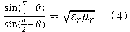
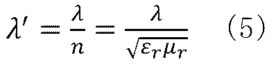


本開示の実施形態3に係る荷電粒子ビームシステム100は、試料に入射されるレーザ光が屈折または伝搬または回折した結果発生する、複数の光の干渉に起因する画像のパターンから、試料の側壁角度または誘電率または光の吸収係数または寸法または側壁の曲率またはボーイングまたはネッキングまたは膜厚または深さの情報を取得する。

プロセッサ302は、モデル解析式を取得する。本実施形態3では、モデル解析式として、式4~6と式8を含む。プロセッサ302は、測定条件を取得する(S802)。本実施形態3では、測定条件として入射角(θ)と波長(λ)と偏光角(φ)を入力する。プロセッサ302は、試料の設計情報を取得する(S803)。本実施形態3では、誘電率(εr)と透磁率(μr)と光の吸収率(k)と穴の直径を設計データライブラリ310から出力しプロセッサ302に入力した。
プロセッサ302は、算出する試料の情報を変数として画像をシミュレーションする。本実施形態3では、算出する試料の情報を側壁角度(α)とした。側壁角度(α)は、側壁の微小領域ごと、具体的には1層分の積層膜の側壁を10分割した微小領域ごとに設定した。
プロセッサ302は、算出した試料の情報を出力したい試料の情報に換算する。本実施形態3では、微小領域ごとの側壁角度(α)と側壁の寸法と側壁の形状を、側壁の曲率とボーイングとネッキングに換算した。算出した試料の情報と出力したい試料の情報が一致している場合、本ステップはスキップしてもよい。
プロセッサ302は、試料の情報とシミュレーションした画像との組をシミュレーションデータライブラリ307のデータベースとして保存する。本実施形態3では、試料の情報として側壁の曲率とボーイングとネッキングを設定した。
本開示の実施形態4に係る荷電粒子ビームシステム100は、試料に入射されるレーザ光と、試料から反射されるレーザ光をミラーで反射させたレーザ光との干渉によって発生する定在波に起因する画像のパターンから、試料の高さまたは膜厚または表面のラフネスまたは表面の曲率または表面のだれまたはスクラッチ欠陥の形状の情報を取得する。
図25は、本開示の実施形態5に係る荷電粒子ビームシステム100の構成図である。統合システムコンピュータ1201は、荷電粒子ビームシステム100と接続されているか、互いに通信可能に構成されている。本実施形態5では統合システムコンピュータ1201がCMP(Chemical Mechanical Polishing)装置1202と互いに通信可能に構成されたシステムを用いたが、CMP装置1202がなくても実施可能である。統合システムコンピュータ1201は、試料の情報から半導体製造装置の推奨条件を出力する。統合システムコンピュータ1201は、荷電粒子ビームシステム100の一部として構成してもよい。なお本実施形態5では図22の試料を用いた。
本開示の実施形態6に係る荷電粒子ビームシステム100は、試料に入射されるレーザ光と、試料から反射されるレーザ光をミラーで反射させたレーザ光との干渉によって発生する定在波に起因する画像のパターンから、試料の欠陥またはボイドの情報を取得する。
本開示の実施形態7に係る荷電粒子ビームシステム100は、試料に照射される電子ビームとレーザ光との遅延時間を変えて取得した、レーザ光との干渉によって発生する定在波に起因する画像のパターンから、試料の拡散速度または移動度の情報を取得する。
走査電子顕微鏡101とレーザ光照射ユニット102との間の遅延時間は、試料に照射される電子ビームとレーザ光との遅延時間と等価であり、レーザ光に対して電子ビームの照射が遅い場合に遅延時間は正、レーザ光に対して電子ビームの照射が早い場合に遅延時間は負である。本実施例では、レーザ光の干渉によって発生する定在波に起因する画像のパターンの位置の時間変化を試料情報抽出プロセッサ305が受け付けることにより、パッシベーション膜を移動するキャリアの拡散速度の位置依存性を出力し、画像のビットマップとして表示した。
本開示の実施形態8に係る荷電粒子ビームシステム100は、試料に照射される電子ビームとレーザ光の照射条件(電子ビームとレーザ光との間の遅延時間、それぞれの強度、それぞれの波長、レーザ光の偏光、それぞれの入射角度)を制御することにより、画像のパターンに重畳するレーザ光の干渉が発生するか否かを切り替える。
本開示の実施形態9に係る荷電粒子ビームシステム100は、試料に入射されるレーザ光と、試料から反射されるレーザ光をミラーで反射させたレーザ光との干渉によって発生する定在波に起因する画像のパターンから、試料の上層のパターンの重心と下層のパターンの重心との間のずれ量に関する情報を取得する。
本開示は、前述した実施形態に限定されるものではなく、様々な変形例が含まれる。例えば、上記した実施形態は本開示を分かりやすく説明するために詳細に説明したものであり、必ずしも説明した全ての構成を備えるものに限定されるものではない。また、ある実施形態の構成の一部を他の実施形態の構成に置き換えることが可能であり、また、ある実施形態の構成に他の実施形態の構成を加えることも可能である。また、各実施形態の構成の一部について、他の構成の追加・削除・置換をすることが可能である。
101:走査電子顕微鏡
102:レーザ光照射ユニット
103:コンピュータシステム
104:同期制御システム
Claims (19)
- 試料に対して荷電粒子ビームを照射することにより前記試料の観察画像を生成する荷電粒子ビームシステムであって、
前記試料に対して前記荷電粒子ビームを照射する荷電粒子源、
前記試料に対して第1光を照射する第1光照射部、
前記試料に対して前記荷電粒子ビームを照射することにより生じる2次荷電粒子を検出してその強度を表す検出信号を出力する検出器、
前記検出信号を用いて前記観察画像を生成するコンピュータシステム、
を備え、
前記コンピュータシステムは、前記試料に対して前記第1光を照射することにより生じる、前記第1光の干渉、前記第1光の回折、または前記第1光の定在波に起因する第1特徴量を、前記観察画像から抽出し、
前記コンピュータシステムは、前記第1特徴量を用いて、前記試料の第2特徴量を取得する
ことを特徴とする荷電粒子ビームシステム。 - 前記コンピュータシステムは、前記第1特徴量として、前記観察画像が有する画像パターンが前記第1光の干渉、前記第1光の回折、または前記第1光の定在波に起因して生じたか否かを判断する基準となるパラメータを記述したデータライブラリを格納する記憶部を備え、
前記コンピュータシステムは、前記画像パターンのうち、前記画像パターンが有する前記パラメータと、前記データライブラリが記述している前記パラメータとの間の一致度が閾値以上であるものを特定し、
前記コンピュータシステムは、前記特定した前記画像パターンが有する前記第1特徴量を用いて、前記第2特徴量を取得する
ことを特徴とする請求項1記載の荷電粒子ビームシステム。 - 前記コンピュータシステムは、前記第1特徴量によって表される関数を用いて前記第2特徴量を記述したデータライブラリを格納する記憶部を備え、
前記コンピュータシステムは、前記第1特徴量を用いて前記データライブラリを参照することにより、前記関数を用いて前記第2特徴量を取得する
ことを特徴とする請求項1記載の荷電粒子ビームシステム。 - 前記コンピュータシステムは、前記第1特徴量として、前記観察画像上において前記第1光の干渉、前記第1光の回折、または前記第1光の定在波に起因して生じる干渉縞パターンの間隔を取得し、
前記コンピュータシステムは、前記観察画像が有する画像パターンのうち、前記画像パターンが有する干渉縞パターンの間隔と、前記取得した前記間隔との間の一致度が閾値以上であるものを特定し、
前記コンピュータシステムは、前記特定した画像パターンが有する干渉縞パターンの間隔を前記第1特徴量として用いて、前記第2特徴量を取得する
ことを特徴とする請求項1記載の荷電粒子ビームシステム。 - 前記コンピュータシステムは、前記第1特徴量として、
前記特定した画像パターンが有する前記干渉縞パターンの間隔、
前記特定した画像パターンが有する前記干渉縞パターンの位置、
のうち少なくともいずれかを取得し、
前記コンピュータシステムは、前記第2特徴量として、前記試料が有するパターンの高さまたは前記試料が有するパターンの側壁の傾斜角度のうち少なくともいずれかを、前記第1特徴量と前記第1光の入射角によって表される関数を用いて計算する
ことを特徴とする請求項4記載の荷電粒子ビームシステム。 - 前記荷電粒子ビームシステムはさらに、前記試料に対して第2光を照射する第2光照射部を備え、
前記コンピュータシステムは、前記第1特徴量として、前記観察画像上において前記第1光と前記第2光が干渉することによって生じる干渉パターンのパワースペクトルを取得し、
前記コンピュータシステムは、前記観察画像が有する画像パターンのうち、前記画像パターンが有する干渉パターンのパワースペクトル、前記取得したパワースペクトルとの間の一致度が閾値以上であるものを特定し、
前記コンピュータシステムは、前記特定した画像パターンが有する干渉パターンのパワースペクトルを前記第1特徴量として用いて、前記第2特徴量を取得する
ことを特徴とする請求項1記載の荷電粒子ビームシステム。 - 前記コンピュータシステムは、前記第2特徴量として、前記試料の誘電率または前記試料の透磁率のうち少なくともいずれかを、
前記試料に対する前記第1光または前記第2光の入射角と、前記試料を前記第1光または前記第2光が通過するときの屈折角とによって表される関数、
および、
前記第1光または前記第2光の波長によって表される関数、
を用いて計算する
ことを特徴とする請求項6記載の荷電粒子ビームシステム。 - 前記コンピュータシステムは、前記第2特徴量として、前記試料の誘電緩和周波数を、
前記荷電粒子ビームの周波数と、空間電過分極が生じている場合における前記試料の誘電率とによって表される関数、
または、
前記第1光または前記第2光の周波数と、電子分極が生じている場合における前記試料の誘電率とによって表される関数、
を用いて計算する
ことを特徴とする請求項7記載の荷電粒子ビームシステム。 - 前記コンピュータシステムは、前記第2特徴量として、前記試料の光吸収係数または前記試料が有するパターンの側壁の傾斜角度のうち少なくともいずれかを、
前記第1光の入射角、前記第1光の波長、前記試料の誘電率、前記試料の透磁率、前記第1光の偏光角、によって表される関数
を用いて計算し、
前記コンピュータシステムは、前記計算した前記側壁の傾斜角度を用いて、前記側壁の形状を計算する
ことを特徴とする請求項1記載の荷電粒子ビームシステム。 - 前記コンピュータシステムは、前記計算した前記側壁の形状を記述したデータライブラリを格納する記憶部を備え、
前記コンピュータシステムは、
前記第1光の入射角、前記第1光の波長、前記試料の誘電率、前記試料の透磁率、前記第1光の偏光角、
のうち少なくともいずれかを用いて前記データライブラリを参照することにより、前記側壁の形状を推定する
ことを特徴とする請求項9記載の荷電粒子ビームシステム。 - 前記荷電粒子ビームシステムはさらに、前記試料から反射した前記第1光を前記試料に対して反射光として再反射する反射ミラーを備え、
前記コンピュータシステムは、前記第1特徴量として、前記観察画像の画素間における前記定在波の位相差を取得する
ことを特徴とする請求項4記載の荷電粒子ビームシステム。 - 前記コンピュータシステムは、前記第2特徴量として、前記試料の表面粗さを表すパラメータを、前記取得した位相差を用いて計算する
ことを特徴とする請求項11記載の荷電粒子ビームシステム。 - 前記コンピュータシステムは、
前記第1特徴量または前記第2特徴量のうち少なくともいずれかと、前記荷電粒子ビームシステムの動作条件として適した動作パラメータとの間の関係を機械学習によって学習する学習器
を実装しており、
前記コンピュータシステムは、前記学習器が出力する前記動作パラメータを用いて、前記荷電粒子ビームシステムの動作を制御する
ことを特徴とする請求項1記載の荷電粒子ビームシステム。 - 前記コンピュータシステムは、前記第1特徴量の局所的ずれと前記第2特徴量との間の関係を記述したデータライブラリを格納する記憶部を備え、
前記データライブラリは、前記第2特徴量として、前記試料が有する欠陥の深さ、前記欠陥の平面位置、前記欠陥の大きさ、のうち少なくともいずれかを記述しており、
前記コンピュータシステムは、前記第1特徴量の局所的変化を取得するとともに、前記取得した局所的ずれを用いて前記データライブラリを参照することにより、前記試料が有する前記欠陥の深さ、前記欠陥の平面位置、前記欠陥の大きさ、のうち少なくともいずれかを取得する
ことを特徴とする請求項1記載の荷電粒子ビームシステム。 - 前記データライブラリは、前記欠陥を有している前記試料の観察画像の画像パターンと、前記欠陥を有していない前記試料の観察画像の画像パターンとをそれぞれ保持しており、
前記コンピュータシステムは、前記検出信号を用いて取得した前記試料の観察画像を前記データライブラリが格納している観察画像と比較することにより、前記試料が前記欠陥を有しているか否かを判定する
ことを特徴とする請求項14記載の荷電粒子ビームシステム。 - 前記コンピュータシステムは、前記第1特徴量の経時変化を取得し、
前記コンピュータシステムは、前記第2特徴量として、前記試料上におけるキャリアの拡散速度または移動度を、前記経時変化の時間変化率を用いて取得する
ことを特徴とする請求項1記載の荷電粒子ビームシステム。 - 前記荷電粒子源または前記第1光照射部のうち少なくともいずれかは、
前記荷電粒子ビームと前記第1光との間の時間差、
前記荷電粒子ビームと前記第1光のうち少なくともいずれかの強度、
前記荷電粒子ビームと前記第1光のうち少なくともいずれかの波長、
前記第1光の偏光、
前記荷電粒子ビームと前記第1光のうち少なくともいずれかの入射角度、
のうち少なくともいずれかを変化させることにより、前記観察画像上において前記第1特徴量を発生させるか否かを切り替える
ことを特徴とする請求項1記載の荷電粒子ビームシステム。 - 前記荷電粒子ビームシステムはさらに、前記試料から反射した前記第1光を前記試料に対して反射光として再反射する反射ミラーを備え、
前記コンピュータシステムは、前記第1特徴量として、前記観察画像の画素値または前記画素値を前記観察画像上の位置によって微分した微分値のうち少なくともいずれかを取得する
ことを特徴とする請求項1記載の荷電粒子ビームシステム。 - 前記コンピュータシステムは、前記第2特徴量として、前記試料上に形成された上層パターンと下層パターンとの間の位置ずれ量を、前記画素値または前記微分値のうち少なくともいずれかを用いて取得する
ことを特徴とする請求項18記載の荷電粒子ビームシステム。
Priority Applications (6)
| Application Number | Priority Date | Filing Date | Title |
|---|---|---|---|
| KR1020237032400A KR102922717B1 (ko) | 2021-03-26 | 2021-03-26 | 하전 입자빔 시스템 |
| CN202180096298.9A CN117043908A (zh) | 2021-03-26 | 2021-03-26 | 带电粒子束系统 |
| JP2023508396A JP7606595B2 (ja) | 2021-03-26 | 2021-03-26 | 荷電粒子ビームシステム |
| US18/283,499 US20240177964A1 (en) | 2021-03-26 | 2021-03-26 | Charged Particle Beam System |
| PCT/JP2021/012996 WO2022201522A1 (ja) | 2021-03-26 | 2021-03-26 | 荷電粒子ビームシステム |
| TW111107642A TWI835084B (zh) | 2021-03-26 | 2022-03-03 | 帶電粒子束系統 |
Applications Claiming Priority (1)
| Application Number | Priority Date | Filing Date | Title |
|---|---|---|---|
| PCT/JP2021/012996 WO2022201522A1 (ja) | 2021-03-26 | 2021-03-26 | 荷電粒子ビームシステム |
Publications (1)
| Publication Number | Publication Date |
|---|---|
| WO2022201522A1 true WO2022201522A1 (ja) | 2022-09-29 |
Family
ID=83396505
Family Applications (1)
| Application Number | Title | Priority Date | Filing Date |
|---|---|---|---|
| PCT/JP2021/012996 Ceased WO2022201522A1 (ja) | 2021-03-26 | 2021-03-26 | 荷電粒子ビームシステム |
Country Status (6)
| Country | Link |
|---|---|
| US (1) | US20240177964A1 (ja) |
| JP (1) | JP7606595B2 (ja) |
| KR (1) | KR102922717B1 (ja) |
| CN (1) | CN117043908A (ja) |
| TW (1) | TWI835084B (ja) |
| WO (1) | WO2022201522A1 (ja) |
Families Citing this family (2)
| Publication number | Priority date | Publication date | Assignee | Title |
|---|---|---|---|---|
| WO2022185390A1 (ja) * | 2021-03-01 | 2022-09-09 | 株式会社日立ハイテク | 荷電粒子線装置 |
| KR20250090336A (ko) * | 2022-12-20 | 2025-06-19 | 주식회사 히타치하이테크 | 시료의 특징량 도출 방법, 신호 처리 시스템을 조정하는 조정 방법 및 계측 시스템 |
Citations (2)
| Publication number | Priority date | Publication date | Assignee | Title |
|---|---|---|---|---|
| JP2000311929A (ja) * | 1999-04-28 | 2000-11-07 | Nec Corp | 半導体集積回路の断線故障検出装置及びその断線故障検出方法 |
| JP2014098815A (ja) * | 2012-11-15 | 2014-05-29 | Ricoh Co Ltd | 静電潜像計測装置、静電潜像計測方法、プログラム及び記録媒体 |
Family Cites Families (11)
| Publication number | Priority date | Publication date | Assignee | Title |
|---|---|---|---|---|
| EP2587515A1 (en) * | 2000-06-27 | 2013-05-01 | Ebara Corporation | Inspection system by charged particle beam and method of manufacturing devices using the system |
| US8203120B2 (en) | 2008-10-09 | 2012-06-19 | California Institute Of Technology | 4D imaging in an ultrafast electron microscope |
| JP5537488B2 (ja) * | 2011-04-15 | 2014-07-02 | 株式会社日立ハイテクノロジーズ | 荷電粒子顕微鏡装置および画像撮像方法 |
| EP2747121A1 (en) * | 2012-12-21 | 2014-06-25 | ICT Integrated Circuit Testing Gesellschaft für Halbleiterprüftechnik mbH | Secondary electron optics & detection device |
| US9418819B2 (en) * | 2013-09-06 | 2016-08-16 | Kla-Tencor Corporation | Asymmetrical detector design and methodology |
| US10037862B2 (en) * | 2015-07-31 | 2018-07-31 | Carl Zeiss Microscopy, Llc | Charged particle detecting device and charged particle beam system with same |
| US11393657B2 (en) | 2018-09-11 | 2022-07-19 | Hitachi High-Tech Corporation | Electron beam device |
| JP7105368B2 (ja) * | 2019-03-27 | 2022-07-22 | 株式会社日立ハイテク | 荷電粒子線装置 |
| JP7203678B2 (ja) * | 2019-04-19 | 2023-01-13 | 株式会社日立ハイテク | 欠陥観察装置 |
| US12437962B2 (en) * | 2020-09-30 | 2025-10-07 | Hitachi High-Tech Corporation | Charged particle beam apparatus |
| JP7582000B2 (ja) * | 2021-03-22 | 2024-11-13 | 株式会社ニューフレアテクノロジー | マルチ荷電粒子ビーム描画装置及びその調整方法 |
-
2021
- 2021-03-26 KR KR1020237032400A patent/KR102922717B1/ko active Active
- 2021-03-26 JP JP2023508396A patent/JP7606595B2/ja active Active
- 2021-03-26 WO PCT/JP2021/012996 patent/WO2022201522A1/ja not_active Ceased
- 2021-03-26 US US18/283,499 patent/US20240177964A1/en active Pending
- 2021-03-26 CN CN202180096298.9A patent/CN117043908A/zh active Pending
-
2022
- 2022-03-03 TW TW111107642A patent/TWI835084B/zh active
Patent Citations (2)
| Publication number | Priority date | Publication date | Assignee | Title |
|---|---|---|---|---|
| JP2000311929A (ja) * | 1999-04-28 | 2000-11-07 | Nec Corp | 半導体集積回路の断線故障検出装置及びその断線故障検出方法 |
| JP2014098815A (ja) * | 2012-11-15 | 2014-05-29 | Ricoh Co Ltd | 静電潜像計測装置、静電潜像計測方法、プログラム及び記録媒体 |
Also Published As
| Publication number | Publication date |
|---|---|
| JP7606595B2 (ja) | 2024-12-25 |
| KR20230148236A (ko) | 2023-10-24 |
| TWI835084B (zh) | 2024-03-11 |
| TW202238654A (zh) | 2022-10-01 |
| KR102922717B1 (ko) | 2026-02-05 |
| CN117043908A (zh) | 2023-11-10 |
| US20240177964A1 (en) | 2024-05-30 |
| JPWO2022201522A1 (ja) | 2022-09-29 |
Similar Documents
| Publication | Publication Date | Title |
|---|---|---|
| CN113614872B (zh) | 用于聚焦带电粒子束的系统和方法 | |
| TWI833979B (zh) | 計量系統及方法 | |
| TWI806955B (zh) | 用於組合之x 射線反射量測術與光電子光譜術之系統及方法 | |
| Orji et al. | Metrology for the next generation of semiconductor devices | |
| KR102235581B1 (ko) | 이미지 합성을 위한 컨볼루션 신경망 기반의 모드 선택 및 결함 분류 | |
| KR20200018824A (ko) | 다색 연엑스선 회절에 기초한 반도체 계측을 위한 방법 및 시스템 | |
| US20130082177A1 (en) | Circuit pattern inspection apparatus and circuit pattern inspection method | |
| CN109298001A (zh) | 电子束成像模块、电子束检测设备及其图像采集方法 | |
| JP7606595B2 (ja) | 荷電粒子ビームシステム | |
| Li et al. | Atomic‐scale strain analysis for advanced Si/SiGe heterostructure by using transmission electron microscopy | |
| US20240353352A1 (en) | Methods And Systems For Nanoscale Imaging Based On Second Harmonic Signal Generation And Through-Focus Scanning Optical Microscopy | |
| TW202424475A (zh) | 使用基於機器學習之電磁回應模型的x射線散射測量之方法及系統 | |
| IL323644A (en) | A method for creating an efficient dynamic sampling plan and accurate reinforcement of test die loss (prob die loss project) | |
| Gin et al. | Inline metrology of high aspect ratio hole tilt using small-angle x-ray scattering | |
| CN116848613A (zh) | 带电粒子束装置 | |
| US12379672B2 (en) | Metrology of nanosheet surface roughness and profile | |
| TW202516562A (zh) | 利用具有cmos陣列下(cua)結構之分類之有效媒體模型之存在cua結構中之計量 | |
| US7102145B2 (en) | System and method for improving spatial resolution of electron holography | |
| Bunday et al. | Metrology | |
| EP4575645A1 (en) | Leed and ptychography based surface profile determination | |
| Çelik et al. | Investigating the influence of FIB-preparation induced surface effects in operando semiconductor TEM-lamellae | |
| Huff | Metrology for Microsystems Manufacturing | |
| Norouzpour | The Development of Self-interference of Split HOLZ (SIS-HOLZ) lines for Measuring z-dependent Atomic Displacement in Crystals | |
| CN121729645A (zh) | 多节距sem套刻标记和缝合区域算法 | |
| Dunin-Borkowski et al. | Electron holography of doped semiconductors: when does it work and is it quantitative? |
Legal Events
| Date | Code | Title | Description |
|---|---|---|---|
| 121 | Ep: the epo has been informed by wipo that ep was designated in this application |
Ref document number: 21933126 Country of ref document: EP Kind code of ref document: A1 |
|
| WWE | Wipo information: entry into national phase |
Ref document number: 2023508396 Country of ref document: JP |
|
| ENP | Entry into the national phase |
Ref document number: 20237032400 Country of ref document: KR Kind code of ref document: A |
|
| WWE | Wipo information: entry into national phase |
Ref document number: 1020237032400 Country of ref document: KR |
|
| WWE | Wipo information: entry into national phase |
Ref document number: 18283499 Country of ref document: US |
|
| WWE | Wipo information: entry into national phase |
Ref document number: 202180096298.9 Country of ref document: CN |
|
| NENP | Non-entry into the national phase |
Ref country code: DE |
|
| 122 | Ep: pct application non-entry in european phase |
Ref document number: 21933126 Country of ref document: EP Kind code of ref document: A1 |