WO2022201227A1 - 基板処理装置、半導体装置の製造方法、及び、プログラム - Google Patents
基板処理装置、半導体装置の製造方法、及び、プログラム Download PDFInfo
- Publication number
- WO2022201227A1 WO2022201227A1 PCT/JP2021/011647 JP2021011647W WO2022201227A1 WO 2022201227 A1 WO2022201227 A1 WO 2022201227A1 JP 2021011647 W JP2021011647 W JP 2021011647W WO 2022201227 A1 WO2022201227 A1 WO 2022201227A1
- Authority
- WO
- WIPO (PCT)
- Prior art keywords
- substrate
- wafer
- heat
- processing apparatus
- heat escape
- Prior art date
- Legal status (The legal status is an assumption and is not a legal conclusion. Google has not performed a legal analysis and makes no representation as to the accuracy of the status listed.)
- Ceased
Links
Images






Classifications
-
- H—ELECTRICITY
- H10—SEMICONDUCTOR DEVICES; ELECTRIC SOLID-STATE DEVICES NOT OTHERWISE PROVIDED FOR
- H10P—GENERIC PROCESSES OR APPARATUS FOR THE MANUFACTURE OR TREATMENT OF DEVICES COVERED BY CLASS H10
- H10P14/00—Formation of materials, e.g. in the shape of layers or pillars
- H10P14/20—Formation of materials, e.g. in the shape of layers or pillars of semiconductor materials
-
- H—ELECTRICITY
- H10—SEMICONDUCTOR DEVICES; ELECTRIC SOLID-STATE DEVICES NOT OTHERWISE PROVIDED FOR
- H10P—GENERIC PROCESSES OR APPARATUS FOR THE MANUFACTURE OR TREATMENT OF DEVICES COVERED BY CLASS H10
- H10P34/00—Irradiation with electromagnetic or particle radiation of wafers, substrates or parts of devices
- H10P34/40—Irradiation with electromagnetic or particle radiation of wafers, substrates or parts of devices with high-energy radiation
- H10P34/42—Irradiation with electromagnetic or particle radiation of wafers, substrates or parts of devices with high-energy radiation with electromagnetic radiation, e.g. laser annealing
Definitions
- the present disclosure relates to a substrate processing apparatus, a semiconductor device manufacturing method, and a program.
- a substrate in a processing chamber is heated using a heating apparatus to change the composition or crystal structure of a thin film formed on the surface of the substrate, or to change the growth.
- a modification treatment represented by an annealing treatment for repairing crystal defects and the like in a thin film.
- An object of the present disclosure is to provide a substrate processing apparatus, a method of manufacturing a semiconductor device, and a program that enable uniform processing of substrates.
- a processing chamber for processing substrates a substrate holder that holds the substrate; a rotation mechanism that rotates the substrate holder; a microwave supply unit for supplying microwaves from one side of the processing chamber when viewed from the rotating shaft of the rotating mechanism to heat the substrate; a loading/unloading unit provided on a side wall facing the microwave supply unit of the processing chamber across the rotation shaft for loading/unloading the substrate; a heat escape suppressing portion disposed between the substrate and the microwave supply portion for suppressing heat escape from an edge of the substrate; is provided.
- FIG. 1 is a vertical cross-sectional view showing a schematic configuration of a substrate processing apparatus suitably used in an embodiment of the present disclosure
- FIG. 1 is a cross-sectional view showing a schematic configuration of a substrate processing apparatus preferably used in an embodiment of the present disclosure
- FIG. 1 is a schematic configuration diagram of a single-wafer processing furnace of a substrate processing apparatus preferably used in an embodiment of the present disclosure, and is a longitudinal sectional view showing a processing furnace portion
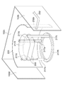
- FIG. FIG. 4 is a perspective view showing the arrangement of a wafer and a heat escape suppression part in a processing chamber of a substrate processing apparatus that is preferably used in the present disclosure
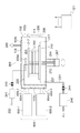
- FIG. 2 is a plan view showing the arrangement of a wafer and a heat escape suppressor in a processing chamber of a substrate processing apparatus that is preferably used in the present disclosure
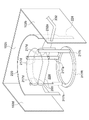
- FIG. 11 is a perspective view showing the arrangement of a wafer and a heat escape suppressing part according to a modification in a processing chamber of a substrate processing apparatus that is preferably used in the present disclosure
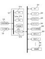
- 1 is a schematic configuration diagram of a controller of a substrate processing apparatus suitably used in the present disclosure
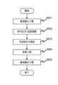
- FIG. FIG. 4 is a diagram showing the flow of substrate processing in the present disclosure
- FIG. 10 is a perspective view showing the arrangement of a wafer and a heat escape suppressing part in a processing chamber according to Modification 1 of a substrate processing apparatus preferably used in the present disclosure
- FIG. 10 is a top view of a boat of Modification 2 of the substrate processing apparatus preferably used in the present disclosure, in which a quartz plate is held;
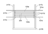
- FIG. 11 is a side view of a state in which a quartz plate is held in a boat of Modified Example 2 of the substrate processing apparatus preferably used in the present disclosure;
- FIG. 11 is a perspective view showing the arrangement of a wafer and a heat escape suppressor in a processing chamber according to Modification 2 of the substrate processing apparatus preferably used in the present disclosure;
- FIG. 11 is a perspective view showing the arrangement of a wafer and a heat escape suppression part in a processing chamber according to Modification 3 of a substrate processing apparatus preferably used in the present disclosure;
- the substrate processing apparatus 100 is configured as a single-wafer heat treatment apparatus that performs various types of heat treatment on wafers, and performs annealing using microwaves, which will be described later. Description will be given as an apparatus for performing (reforming treatment).
- a FOUP Front Opening Unified Pod: hereinafter referred to as a pod
- Pod 110 is used as a storage container (carrier) containing wafers 200 as substrates.
- Pod 110 is also used as a transport container for transporting wafers 200 between various substrate processing apparatuses.
- the substrate processing apparatus 100 includes a transfer case (case) 202 having therein a transfer chamber (transfer area) 203 for transferring a wafer 200, and a side wall of the transfer case 202. It is provided with cases 102-1 and 102-2 as processing containers, which will be described later, and which have processing chambers 201-1 and 201-2 for processing wafers 200, respectively.
- 1 (lower side in FIG. 2), which is the front side of the housing of the transfer chamber 203, is a pod for opening and closing the lid of the pod 110 and transferring/unloading the wafer 200 to/from the transfer chamber 203.
- a load port unit (LP) 106 is arranged as an opening/closing mechanism.
- the load port unit 106 includes a housing 106a, a stage 106b, and an opener 106c.
- the stage 106b is configured to place the pod 110 thereon and bring the pod 110 close to a substrate loading/unloading port 134 formed in front of the housing of the transfer chamber 203, and is provided on the pod 110 by an opener 106c (not shown). Open and close the lid.
- the housing 202 has a purge gas circulation structure provided with a clean unit 166 for circulating a purge gas such as N 2 in the transfer chamber 203 .
- Gate valves 205-1 and 205-2 for opening and closing the processing chambers 201-1 and 202-2 are provided on the left side in FIG. placed respectively.
- a transfer machine 125 serving as a substrate transfer mechanism (substrate transfer robot) for transferring the wafer 200 is installed in the transfer chamber 203 .
- the transfer device 125 can horizontally rotate or linearly move tweezers (arms) 125a-1 and 125a-2 as mounting units for mounting the wafer 200, and tweezers 125a-1 and 125a-2. It is composed of a transfer device 125b and a transfer device elevator 125c for raising and lowering the transfer device 125b.
- wafers 200 are loaded (charged) or unloaded (discharged) from substrate holders (boats) 217 and pods 110, which will be described later.
- It has a configuration that allows Hereinafter, the cases 102-1 and 102-2, the processing chambers 201-1 and 201-2, and the tweezers 125a-1 and 125a-2 are simply referred to as the case 102, the processing Chamber 201 is described as tweezers 125a.
- a wafer cooling mount 108 for cooling the processed wafer 200 is provided on a wafer cooling table 109 in a space above the transfer chamber 203 and below the clean unit 166 .
- the wafer cooling mount 108 has the same structure as a boat 217 as a substrate holder, which will be described later, and horizontally holds a plurality of wafers 200 vertically in multiple stages by means of a plurality of wafer holding grooves (holding portions).
- the wafer cooling mount 108 and the wafer cooling table 109 are provided above the installation positions of the substrate loading/unloading port 134 and the gate valve 205 , so that the wafer 200 can be transferred from the pod 110 to the processing chamber 201 by the transfer device 125 . It is possible to cool the processed wafer 200 without lowering the throughput of the wafer processing because it is out of the line of flow during transportation.
- the wafer cooling table 108 and the wafer cooling table 109 may be collectively referred to as a cooling area (cooling region).
- the pressure in the pod 110, the pressure in the transfer chamber 203, and the pressure in the processing chamber 201 are all controlled at atmospheric pressure or a pressure higher than atmospheric pressure by about 10 to 200 Pa (gauge pressure).
- the pressure in the transfer chamber 203 is higher than the pressure in the processing chamber 201 and the pressure in the processing chamber 201 is higher than the pressure in the pod 110 .
- a processing furnace having a substrate processing structure as shown in FIG. 3 is constructed in an area A surrounded by a dashed line in FIG. As shown in FIG. 2, a plurality of processing furnaces are provided in this embodiment, but since the structures of the processing furnaces are the same, only one structure will be described, and the description of the other processing furnace structure will be omitted. do.
- the processing furnace has a case 102 as a cavity (processing container) made of a material that reflects microwaves, such as metal.
- the case 102 has a substantially rectangular parallelepiped box shape, and has four side surfaces and side walls 102a, 102b, 102c, and 102d.
- a cap flange (closure plate) 104 made of a metal material is provided on the ceiling surface of the case 102 to block the ceiling surface of the case 102 via an O-ring (not shown) as a sealing member (seal member).
- the space inside the case 102 and the cap flange 104 is mainly configured as a processing chamber 201 for processing substrates such as silicon wafers.
- the processing chamber 201 may be configured using the case 102 with a closed ceiling without providing the cap flange 104 .
- a mounting table 210 is provided in the processing chamber 201, and a boat 217 as a substrate holding unit for holding a wafer 200 as a substrate is mounted on the upper surface of the mounting table 210.
- the boat 217 includes a ring 217R and boat pillars (holding pillars) 217a-217c.
- the bottom ring 217R has an annular shape, and the boat posts 217a to 217c are erected at intervals on the circumference of the bottom ring 217R.
- Each of the boat columns 217a to 217c is provided with a wafer holding portion 217d for holding the wafer 200 on the side surface on the wafer center side (diametrically inner side facing each other).
- Susceptors 103a and 103b such as silicon plates (Si plates) and silicon carbide plates (SiC plates), may be placed so as to sandwich the wafer 200 therebetween.
- the case 102 as a processing container has a substantially rectangular parallelepiped shape in this embodiment, it may be configured as a flat closed container having a circular cross section, for example.
- the transport case 202 is made of a metal material such as aluminum (Al) or stainless steel (SUS).
- the space surrounded by the case 102 may be referred to as a processing chamber 201 or reaction area 201 as a processing space, and the space surrounded by the transport housing 202 may be referred to as a transport chamber 203 or transport area 203 as a transport space. .
- a substrate loading/unloading port 206 adjacent to the gate valve 205 is provided on the side surface of the transport housing 202, and a loading/unloading port 207 is provided on the side wall 102a of the case 102. is provided.
- the wafer 200 moves between the processing chamber 201 and the transfer chamber 203 via the substrate loading/unloading port 206 and the loading/unloading port 207 .
- the side wall 102c of the case 102 is provided with a microwave supply unit 600, which will be described in detail later. 200 are processed.
- the mounting table 210 is supported by a shaft 255 as a rotating shaft.
- the shaft 255 passes through the bottom of the case 102 and is connected to a drive mechanism 267 that rotates outside the transport container 202 .
- a rotation mechanism is configured by the mounting table 210 , the shaft 255 and the drive mechanism 267 .
- the lower end of the shaft 255 is covered with a bellows 212 so that the processing chamber 201 and the transfer area 203 are kept airtight.
- the mounting table 210 is raised or lowered by the drive mechanism 267 according to the height of the substrate loading/unloading port 206 so that the wafer 200 is at the wafer transport position when the wafer 200 is transported, and when the wafer 200 is processed, the wafer 200 is moved downward.
- An exhaust section for exhausting the atmosphere of the processing chamber 201 is provided below the processing chamber 201 and on the outer peripheral side of the mounting table 210 . As shown in FIG. 3, an exhaust port 221 is provided in the exhaust portion. An exhaust pipe 231 is connected to the exhaust port 221. In the exhaust pipe 231, a pressure regulator 244 such as an APC valve that controls the valve opening according to the pressure inside the processing chamber 201, and a vacuum pump 246 are connected in series. It is connected to the.
- a pressure regulator 244 such as an APC valve that controls the valve opening according to the pressure inside the processing chamber 201, and a vacuum pump 246 are connected in series. It is connected to the.
- the pressure regulator 244 is not limited to an APC valve as long as it can receive pressure information (a feedback signal from a pressure sensor 245, which will be described later) in the processing chamber 201 and adjust the exhaust amount.
- the on-off valve and the pressure regulating valve may be used together.
- the exhaust port 221, the exhaust pipe 231, and the pressure regulator 244 mainly constitute an exhaust section (also referred to as an exhaust system or an exhaust line).
- An exhaust port may be provided so as to surround the mounting table 210 so that gas can be exhausted from the entire periphery of the wafer 200 .
- a vacuum pump 246 may be added to the configuration of the exhaust section.
- a side wall 102b of the case 102 is connected to a gas supply pipe 232 for supplying processing gases for various substrate processing such as inert gas, raw material gas, and reaction gas into the processing chamber 201 .
- the gas supply pipe 232 is provided with a mass flow controller (MFC) 241 as a flow controller (flow control unit) and a valve 243 as an on-off valve in order from upstream.
- MFC mass flow controller
- N2 nitrogen
- the gas supply pipe 232 is provided with an MFC, which is a flow rate controller, and a valve, which is an on-off valve, downstream of the valve 243 in the gas supply pipe 232 in this order from the upstream side.
- MFC mass flow controller
- N2 nitrogen
- the gas supply pipe 232 is provided with an MFC, which is a flow rate controller, and a valve, which is an on-off valve, downstream of the valve 243 in the gas supply pipe 232 in this order from the upstream side.
- a plurality of types of gas can be supplied by using the configuration in which the supply pipes are connected.
- a gas supply pipe provided with an MFC and a valve may be installed for each gas type. Also, the gas supply pipe 232 may be connected to the cap flange 104 .
- a gas supply system (gas supply unit) is mainly composed of the gas supply pipe 232 , the MFC 241 and the valve 243 .
- an inert gas When an inert gas is passed through the gas supply system, it is also called an inert gas supply system.
- the inert gas in addition to N2 gas, for example, rare gases such as Ar gas, He gas, Ne gas, and Xe gas can be used.
- a temperature sensor 263 is installed on the cap flange 104 as a non-contact temperature measuring device. By adjusting the output of a microwave oscillator 655, which will be described later, based on the temperature information detected by the temperature sensor 263, the substrate is heated and the substrate temperature has a desired temperature distribution.
- the temperature sensor 263 is composed of a radiation thermometer such as an IR (Infrared Radiation) sensor, for example.
- a temperature sensor 263 is installed to measure the surface temperature of the wafer 200 . If the susceptor described above is provided, the surface temperature of the susceptor may be measured.
- the temperature of the wafer 200 means the wafer temperature converted by temperature conversion data to be described later, that is, the estimated wafer temperature. Description will be made assuming that it means the temperature obtained by directly measuring the temperature of the wafer 200 and that it means both of them.
- thermocouple may be used for temperature measurement, or a thermocouple and a non-contact thermometer may be used together to measure the temperature.
- a thermocouple it is necessary to place the thermocouple near the wafer 200 to measure the temperature. That is, since the thermocouple must be arranged in the processing chamber 201, the thermocouple itself is heated by the microwaves supplied from the microwave oscillator 655, which will be described later, so the temperature cannot be measured accurately. Therefore, it is preferable to use a non-contact thermometer as the temperature sensor 263 .
- the temperature sensor 263 is not limited to being provided on the cap flange 104 and may be provided on the mounting table 210 . Moreover, the temperature sensor 263 is not only directly installed on the cap flange 104 and the mounting table 210, but also measures indirectly by reflecting radiation light from a measurement window provided on the cap flange 104 and the mounting table 210 with a mirror or the like. may be configured to Furthermore, the number of temperature sensors 263 is not limited to one, and a plurality of temperature sensors may be installed.
- Microwave introduction ports 653-1 and 653-2 are installed on the side wall 102c on the side opposite to the loading/unloading port 207 with the shaft 255 of the case 102 interposed therebetween.
- One ends of waveguides 654-1 and 654-2 for supplying microwaves into the processing chamber 201 are connected to the microwave introduction ports 653-1 and 653-2, respectively.
- Microwave oscillators (microwave sources) 655-1 and 655-2 are connected to the other ends of the waveguides 654-1 and 654-2, respectively. ing.
- Microwave oscillators 655-1, 655-2 supply microwaves to waveguides 654-1, 654-2, respectively.
- a magnetron, a klystron, or the like is used for the microwave oscillators 655-1 and 655-2.
- microwave introduction ports 653-1 and 653-2, waveguides 654-1 and 654-2, and microwave oscillators 655-1 and 655-2 will be described unless it is necessary to distinguish between them.
- a microwave introduction port 653 a waveguide 654 and a microwave oscillator 655 .
- the frequency of microwaves generated by microwave oscillator 655 is preferably controlled to be in the frequency range of 13.56 MHz to 24.125 GHz. More preferably, the frequency is controlled to be 2.45 GHz or 5.8 GHz.
- the respective frequencies of the microwave oscillators 655-1 and 655-2 may be the same frequency, or may be set at different frequencies.
- microwave oscillators 655 are arranged on the side surface of the case 102, but this is not a limitation, and one or more may be arranged.
- microwave generator 655-1, 655-2, waveguide 654-1, 654-2 and microwave introduction port 653-1, 653-2 microwave supply unit 600 is constructed.
- a controller 121 which will be described later, is connected to each of the microwave oscillators 655-1 and 655-2.
- a temperature sensor 263 for measuring the temperature of the quartz plate 101 a or 101 b housed in the processing chamber 201 or the wafer 200 is connected to the controller 121 .
- the temperature sensor 263 measures the temperature of the quartz plate 101, susceptor 103, or wafer 200 by the method described above, transmits the temperature to the controller 121, and the controller 121 controls the outputs of the microwave oscillators 655-1 and 655-2. , controls the heating of the wafer 200 .
- the microwave oscillators 655-1 and 655-2 are controlled by the same control signal transmitted from the controller 121.
- the configuration is not limited to this, and the microwave oscillators 655-1 and 655-2 are individually controlled by transmitting individual control signals from the controller 121 to each of the microwave oscillators 655-1 and 655-2. You may
- a heat escape suppression unit 220 is provided in the processing chamber 201 .
- the heat escape suppression part 220 is arranged between the wafer 200 and the microwave introduction ports 653-1 and 653-2.
- the heat escape suppressing portion 220 has a semi-cylindrical shape and is arranged along the outer circumference of the wafer 200 .
- the heat escape suppressing portion 220 has a semi-annular shape when viewed from the axial direction of the shaft 255 (in a plan view), and the portion corresponding to the microwave supplying portion 600 is located in the middle of the semi-annular ring. It is arranged to be a part.
- the heat escape suppressing portion 220 has a shape in which an opening 222 is formed toward the carry-in/out port 207 side.
- the heat escape suppression part 220 can be formed of a member that transmits microwaves or a member that generates heat by absorbing microwaves. In this embodiment, it is made of quartz as an example.
- the heat escape suppressing portion 220 has a semicircular shape in plan view.
- the shape is not limited to a semi-circular shape, and other shapes may be used.
- the heat escape suppressing part 220 since the cooling gas (N2) is introduced from the gas supply pipe 232 connected to the side wall 102b of the processing chamber 201, the heat escape suppressing part 220 has the cooling gas introduction portion 232a. It is preferable to have a shape that does not get stuck. By not arranging the heat escape suppression part 220 at the position corresponding to the introduction part 232a of the cooling gas, the cooling efficiency when cooling the processing chamber 201 can be maintained.
- the heat escape suppressing portion 220 may form an open portion 224 by notching a portion where the wafers 200 are not arranged in the axial direction of the shaft 255 (the stacking direction of the wafers 200). good.
- the opening 224 is provided on the side where the microwave supply section 600 is arranged (the side opposite to the loading/unloading port 207). By forming the opening 224 in this way, it is possible to improve the efficiency of supplying microwaves to the wafer 200 while suppressing heat escape from the edge of the wafer 200 .
- a controller 121 which is a control unit (control device, control means), includes a CPU (Central Processing Unit) 121a, a RAM (Random Access Memory) 121b, a storage device 121c, and an I/O port 121d. Configured as a computer.
- the RAM 121b, storage device 121c, and I/O port 121d are configured to exchange data with the CPU 121a via an internal bus 121e.
- An input/output device 122 configured as, for example, a touch panel or the like is connected to the controller 121 .
- the storage device 121c is composed of, for example, a flash memory, HDD (Hard Disk Drive), or the like.
- a control program for controlling the operation of the substrate processing apparatus, a process recipe describing procedures and conditions of annealing (modification) processing, and the like are stored in a readable manner.
- the process recipe functions as a program in which the controller 121 executes each procedure in the substrate processing process described below and is combined so as to obtain a predetermined result.
- the process recipe, the control program, and the like are collectively referred to simply as the program.
- the process recipe is simply called a recipe.
- the RAM 121b is configured as a memory area (work area) in which programs and data read by the CPU 121a are temporarily held.
- the I/O port 121d is connected to the MFC 241, the valve 243, the pressure sensor 245, the APC valve 244, the vacuum pump 246, the temperature sensor 263, the driving mechanism 267, the microwave oscillator 655, and the like.
- the CPU 121a is configured to be able to read and execute a control program from the storage device 121c, and read recipes from the storage device 121c in response to input of operation commands from the input/output device 122, and the like.
- the CPU 121a adjusts the flow rate of various gases by the MFC 241, the opening and closing operation of the valve 243, the pressure adjustment operation by the APC valve 244 based on the pressure sensor 245, the start and stop of the vacuum pump 246, the temperature It is configured to be able to control the output adjustment operation of the microwave oscillator 655 based on the sensor 263, the rotation and rotation speed adjustment operation of the mounting table 210 (or the boat 217) by the drive mechanism 267, or the up-and-down operation.
- the controller 121 installs the above-described program stored in an external storage device (for example, a magnetic disk such as a hard disk, an optical disk such as a CD, a magneto-optical disk such as an MO, a USB memory, a semiconductor memory such as an SSD) 123 into a computer.
- an external storage device for example, a magnetic disk such as a hard disk, an optical disk such as a CD, a magneto-optical disk such as an MO, a USB memory, a semiconductor memory such as an SSD
- the storage device 121c and the external storage device 123 are configured as computer-readable recording media. Hereinafter, these are also collectively referred to simply as recording media.
- recording medium When the term "recording medium" is used in this specification, it may include only the storage device 121c alone, may include only the external storage device 123 alone, or may include both of them.
- the program may be provided to the computer using communication means such as the Internet or a dedicated line without using the external storage device 123 .
- the word "wafer” when used in this specification, it may mean the wafer itself, or it may mean a laminate of a wafer and a predetermined layer or film formed on its surface.
- the term “wafer surface” may mean the surface of the wafer itself or the surface of a predetermined layer formed on the wafer.
- the term "formation of a predetermined layer on a wafer” means that a predetermined layer is formed directly on the surface of the wafer itself, or a layer formed on the wafer, etc. It may mean forming a given layer on top of.
- substrate in this specification is synonymous with the use of the term "wafer”.
- Substrate loading step (S501) As shown in FIG. 3, a wafer 200 placed on one or both of the tweezers 125a-1 and 125a-2 is loaded into a predetermined processing chamber 201 by opening and closing the gate valve 205. (S501).
- the atmosphere inside the processing chamber 201 is controlled so that the inside of the processing chamber 201 has a predetermined pressure (for example, 10 to 102000 Pa).
- a predetermined pressure for example, 10 to 102000 Pa.
- the valve opening degree of the pressure regulator 244 is feedback-controlled based on the pressure information detected by the pressure sensor 245 to set the inside of the processing chamber 201 to a predetermined pressure.
- the microwave supply unit may be controlled as preheating so that heating is performed up to a predetermined temperature (S502).
- the microwave supply unit When the temperature is raised to a predetermined substrate processing temperature by the microwave supply unit, it is preferable to raise the temperature with an output smaller than the output of the modification process described later so that the wafer 200 is not deformed or damaged.
- control may be performed such that after only adjusting the temperature in the furnace without adjusting the pressure in the furnace, the process proceeds to the inert gas supply step S503, which will be described later.
- the microwave oscillator 655 supplies microwaves into the processing chamber 201 through the components described above.
- the microwaves are supplied into the processing chamber 201 while passing through the heat escape suppressing portion 220 .
- the wafer 200 is heated to a temperature of 100° C. or more and 1000° C. or less, preferably 400° C. or more and 900° C. or less, more preferably 500° C. or more and 700° C. or less. Heat until By processing the substrate at such a temperature, the wafer 200 is processed at a temperature at which microwaves are efficiently absorbed, and the speed of the modification processing can be improved.
- the wafer 200 is processed at a temperature lower than 100° C. or higher than 1000° C., the surface of the wafer 200 will change in quality, making it difficult to absorb microwaves. Therefore, it becomes difficult to heat the wafer 200 immediately. Therefore, it is desirable to process the substrate in the temperature range described above.
- an inert gas (N2 as an example) may be supplied from the gas supply pipe 232 as a cooling gas.
- the temperature of the wafer 200 tends to be high at the center in the radial direction, and tends to be low at the outer edge portion in the radial direction due to heat dissipation. Since the heat escape suppressing portion 220 is arranged so as to surround the outer periphery of the wafer 200 by half the circumference, the outer peripheral portion is kept warm, and heat escape from the edge of the wafer 200 can be suppressed. Thereby, the heat uniformity of the entire wafer 200 can be improved.
- the heat escape suppressing portion 220 is not arranged on the outer periphery of the wafer 200, since the wafer 200 rotates around the shaft 255 as a rotation axis, it is possible to ensure the uniformity of heat at the edge portion of the wafer 200. .
- the microwave oscillator 655 By controlling the microwave oscillator 655 as described above, the wafer 200 is heated and the amorphous silicon film formed on the surface of the wafer 200 is reformed (crystallized) into a polysilicon film (S504). That is, the wafer 200 can be uniformly modified. Note that when the measured temperature of the wafer 200 exceeds the above-described threshold value and becomes higher or lower, the output of the microwave oscillator 655 is controlled to be low instead of turning off the microwave oscillator 655. may fall within a predetermined range. In this case, the output of the microwave oscillator 655 is controlled to increase when the temperature of the wafer 200 returns to within a predetermined range.
- the wafer 200 is reformed, and the next substrate processing process is started.
- the heat escape suppressing portion 220 suppresses heat escape from the outer peripheral edge of the wafer 200, so that the wafer 200 can be processed uniformly.
- the substrate processing apparatus according to the present embodiment is not limited to the above aspect, and can be modified as in the modifications shown below.
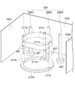
- Modification 1 Modification 1 of the present embodiment will be described below. As shown in FIG. 9, in Modification 1, heat escape suppression bars 226A, 226B, and 226C are provided instead of the heat escape suppression portion 220 in the above-described embodiment.
- the heat escape suppression rods 226A, 226B, and 226C are made of a member that absorbs microwaves and generates heat. As an example, it can be made of silicon carbide (SiO).
- the heat escape suppression rods 226A, 226B, and 226C are collectively referred to as the heat escape suppression rod 226.
- the heat escape suppression bar 226 is shaped like a bar extending in the rotational axis direction of the wafer 200 and has a base portion 227 formed at its lower end.
- the heat escape suppression rods 226 are spaced apart from each other between the microwave supply unit 600 and the wafer 200 and arranged radially outside the wafer 200 along the outer circumference of the wafer 200 .
- the heat escape suppression bar 226 absorbs the microwaves and generates heat, so that the edge portion of the wafer 200 is heated by the secondary heat generation, and the temperature uniformity within the surface of the wafer 200 can be improved. can. Moreover, since the heat escape suppression bar 226 is rod-shaped, the microwaves from the microwave supply unit 600 can be efficiently supplied to the wafer 200 without being blocked by the heat escape suppression bar 226 .
- three heat escape suppression bars 226A, 226B, and 226C are installed, but one, two, or four or more may be installed.
- the heating effect can be enhanced by installing a plurality of the heaters.
- the boat 217 includes wafers 200 to be processed and quartz plates as heat insulating plates placed vertically above and below the wafers 200 so as to sandwich the wafers 200 .
- Plates 101a and 101b are held at predetermined intervals.
- Susceptors 103a and 103b such as silicon plates (Si plates) and silicon carbide plates (SiC plates) may be placed between the quartz plates 101a and 101b and the wafer 200, respectively.
- the quartz plates 101a and 101b and the susceptors 103a and 103b are the same parts, respectively, and will be referred to as the quartz plate 101 and the susceptor 103 unless they need to be distinguished from each other. do.
- the boat 217 includes a ring 217R and boat pillars (holding pillars) 217a to 217c.
- the bottom ring 217R has an annular shape, and the boat posts 217a to 217c are erected at intervals on the circumference of the bottom ring 217R.
- Each of the boat columns 217a to 217c has a wafer holding part 217d for holding the wafer 200, the quartz plate 101, and the susceptor 103 on the wafer center side (diametrically inner side facing each other) along the length of the boat columns 217a to 217c. They are provided at six locations spaced apart in the direction (vertical direction).
- a vertical interval between the wafer holding portions 217d is, for example, about 5 mm to 15 mm.
- the two disk-shaped wafers 200 are held by vertically adjacent wafer holding portions 217d, and arranged inside the boat pillars 217a to 217c so that the plate surfaces face up and down.
- the susceptor 103 is held by the wafer holding part 217d at a position sandwiching the two disk-shaped wafers 200 from above and below, and is arranged inside the boat columns 217a to 217c such that the plate surfaces face up and down. be.
- the susceptor 103 is formed of a silicon plate or the like, absorbs microwaves, generates heat, and indirectly heats the wafer 200 .
- the quartz plate 101a is annular (ring-shaped) and has a first ring plate 101a1 and a second ring plate 101a2 as a heat insulating member.
- the first ring plate 101a1 and the second ring plate 101a2 also have an annular shape (ring shape) through which the central portion penetrates (having a through hole H in the central portion).
- the inner diameter of the first ring plate 101a1 is larger than or substantially the same as the outer diameter of the second ring plate 101a2, and the second ring plate 101a2 is arranged concentrically inside the first ring plate 101a1.
- the quartz plate 101b has the same shape as the quartz plate 101a, and has a first ring plate 101b1 and a second ring plate 101b2 as a heat insulating member.
- the second ring plate 101 a 2 is held by the upper wafer holder 217 d and placed on the wafer 200 and susceptor 103 .
- the second ring plate 101b2 is held by the lower wafer holding portion 217d and placed below the wafer 200 and the susceptor 103. As shown in FIG.
- each of the second ring plates 101a2 and 101b2 is formed with holding portions 112a, 112b and 112c projecting radially outward from the outer periphery.
- the upper surface of the holding portion 112a is arranged on substantially the same plane as the lower surface of the second ring plate 101a2. The same applies to the upper surfaces of the holding portions 112b, 112b.
- the outer diameter of the first ring plates 101a1 and 101b1 is larger than that of the wafer 200. Cutouts 101k are formed on the inner periphery of the first ring plates 101a1 and 101b1 at positions corresponding to the boat pillars 217a to 217c away from each other in the circumferential direction. By arranging the boat pillars 217a to 217c to pass through the notch 101k, the inner peripheries of the first ring plates 101a1 and 101b1 can be brought closer to the outer peripheries of the second ring plates 101a2 and 101b2.
- the first ring plates 101a1 and 101b1 are respectively held from below by holding portions 112a, 112b and 112c.
- quartz plate 101 it is preferable to use one that has a high heat ray (light) reflectance.
- a high heat ray (light) reflectance For example, opaque quartz, transparent quartz with a roughened surface, and quartz in which air bubbles are added to increase the heat ray (light) reflectance can be used.
- the heat ray (light) reflectance of ordinary quartz is about 5%
- quartz having a heat ray (light) reflectance of about 50% Since quartz itself transmits microwaves, it is not directly heated. The function of keeping the wafer 200 and susceptor 103 warm can be enhanced.
- the quartz plate 101 and the boat 217 By configuring the quartz plate 101 and the boat 217 in this way and arranging the wafer 200, the susceptor 103, and the quartz plate 101, as shown in FIG. (positions where they do not touch). Further, the quartz plate 101 is arranged so that the outer peripheral portion of the quartz plate 101 is located radially outside the outer peripheral portion (also referred to as an end portion, an edge portion, or a peripheral edge portion) of the wafer 200 . Also, the wafer 200 is arranged in a state where the central portion thereof is not covered with the quartz plate 101 . The outer peripheral portion of the quartz plate 101 keeps the outer peripheral portion of the wafer 200 warm in combination with the heat retention by the heat escape suppression portion 220 . Also, heat can be released from the center of the wafer 200 . As a result, the heat distribution of the wafer 200 can be made uniform, and the uniformity of the modification of the wafer 200 can be improved.
- the quartz plate 101 has been described as having a ring shape with a circular outer periphery, but the outer periphery shape is not limited to this, and may be polygonal or any other shape. .
- temperature changes of the quartz plate 101 or the susceptor 103 and the wafer 200 are acquired in advance by the temperature sensor 263 , so that the temperatures of the quartz plate 101 or the susceptor 103 and the wafer 200 are obtained.
- the temperature of the wafer 200 can be estimated by measuring only the temperature of the quartz plate 101, and based on the estimated temperature of the wafer 200, , the output of the microwave oscillator 655, that is, the heating device can be controlled.
- Modification 3 Modification 3 of the present embodiment will be described below.
- a heat escape restraint bar 226 is provided in place of the heat escape restraint portion 220, and as in Modification 2, the quartz plates 101a and 101b and the susceptor 103a and 103b are arranged.
- the heat escape suppression bar 226 absorbs microwaves and generates heat, so that the edge portion of the wafer 200 is heated by the secondary heat generation, and the temperature uniformity within the surface of the wafer 200 can be improved. can. Moreover, since the heat escape suppression bar 226 is rod-shaped, the microwaves from the microwave supply unit 600 can be efficiently supplied to the wafer 200 without being blocked by the heat escape suppression bar 226 .
- the outer circumference of the wafer 200 is kept warm by the outer circumference of the quartz plate 101 together with the heating by the heat escape suppression bar 226 . Also, heat can be released from the center of the wafer 200 . As a result, the heat distribution of the wafer 200 can be made uniform, and the uniformity of the modification of the wafer 200 can be improved.
- a configuration has been described in which a plurality of wafers 200 are collectively processed at the same time by placing two wafers 200 on the boat 217 .
- the present invention is not limited to this, and one wafer 200 may be placed on the boat 217 for processing, or the wafer 200 and a dummy wafer (not shown) may be placed on the boat 217 for processing.
- the heat capacity in the processing chamber can be made close to the heat capacity in the processing chamber when two wafers 200 are placed and processed, and one wafer 200 can be placed and processed. Even if it does, it is possible to obtain the same processing result.
- oxygen (O) and nitrogen (N) , carbon (C), and hydrogen (H) may be supplied to modify the film formed on the surface of the wafer 200 .
- oxygen (O) and nitrogen (N) , carbon (C), and hydrogen (H) may be supplied to modify the film formed on the surface of the wafer 200 .
- HfxOy film hafnium oxide film
- by supplying microwaves while supplying gas containing oxygen to heat the hafnium oxide film can replenish the deficient oxygen, and improve the characteristics of the high dielectric film.
- hafnium oxide film is shown here, it is not limited to this, and aluminum (Al), titanium (Ti), zirconium (Zr), tantalum (Ta), niobium (Nb), lanthanum (La), cerium (Ce), yttrium (Y), barium (Ba), strontium (Sr), calcium (Ca), lead (Pb), molybdenum (Mo), tungsten (W), etc. It can also be suitably applied when modifying a film, that is, a metal-based oxide film.
- the above-described film formation sequence is such that a TiOCN film, a TiOC film, a TiON film, a TiO film, a ZrOCN film, a ZrOC film, a ZrON film, a ZrO film, an HfOCN film, an HfOC film, an HfON film, and an HfO film are formed on the wafer 200.
- films containing silicon as a main component include silicon nitride films (SiN films), silicon oxide films (SiO films), silicon oxycarbide films (SiOC films), silicon oxycarbonitride films (SiOCN films), silicon oxynitride films (SiON films). film) and other Si-based oxide films.
- Impurities include, for example, at least one of bromine (B), carbon (C), nitrogen (N), aluminum (Al), phosphorus (P), gallium (Ga), arsenic (As), and the like.
- PMMA methyl methacrylate
- epoxy resin epoxy resin
- novolak resin novolak resin
- polyvinyl phenyl resin and the like.
- the present invention is not limited to this, and patterning processing in the manufacturing process of liquid crystal panels, patterning processing in the manufacturing process of solar cells, and patterning processing in the manufacturing process of power devices. It is also applicable to techniques for processing substrates, such as.
- Substrate processing apparatus 101 Quartz plate (insulating member) 200 wafer (substrate) 201 processing chamber 217 substrate holder 210 mounting table (rotating mechanism) 255 shaft (rotating shaft, rotating mechanism) 267 drive mechanism (rotation mechanism) 600 microwave supply unit 207 carrying-in/out unit 220 heat escape suppressing unit 222 opening 224 opening 226 heat escape suppressing rod (heat escape suppressing unit) 232 gas supply pipe (cooling gas supply unit)
Abstract
基板処理装置は、基板を処理する処理室と、基板を保持する基板保持部と、基板保持部を回転させる回転機構と、回転機構の回転軸から見て、処理室の一方側からマイクロ波を供給し、基板を加熱処理するマイクロ波供給部と、回転軸を挟んで処理室のマイクロ波供給部に対向する側壁に設けられ、基板を搬入出する搬入出部と、基板とマイクロ波供給部との間に配置され、基板のエッジからの熱逃げを抑制する熱逃げ抑制部と、を備えている。
Description
本開示は、基板処理装置、半導体装置の製造方法、及び、プログラムに関するものである。
半導体装置(半導体デバイス)の製造工程の一工程として、例えば、加熱装置を用いて処理室内の基板を加熱し、基板の表面に成膜された薄膜中の組成や結晶構造を変化させたり、成膜された薄膜内の結晶欠陥等を修復したりするアニール処理に代表される改質処理がある。近年の半導体デバイスにおいては、微細化、高集積化が著しくなっており、これに伴い、高いアスペクト比を有するパターンが形成された高密度の基板への改質処理が求められている。このような高密度基板への改質処理方法としてマイクロ波を用いた熱処理方法が検討されている。一例として、特許文献1に記載の技術が挙げられる。
従来のマイクロ波を用いた処理では、基板等の処理室内部構成部品の径方向外側より熱が逃げ、基板を均一に改質処理することが困難となってしまう場合がある。
本開示の目的は、基板を均一に処理することが可能となる、基板処理装置、半導体装置の製造方法、及び、プログラムを提供することにある。
本開示の一態様によれば、
基板を処理する処理室と、
前記基板を保持する基板保持部と、
前記基板保持部を回転させる回転機構と、
前記回転機構の回転軸から見て前記処理室の一方側からマイクロ波を供給し、前記基板を加熱処理するマイクロ波供給部と、
前記回転軸を挟んで前記処理室の前記マイクロ波供給部に対向する側壁に設けられ、前記基板を搬入出する搬入出部と、
前記基板と前記マイクロ波供給部との間に配置され、前記基板のエッジからの熱逃げを抑制する熱逃げ抑制部と、
を有する技術が提供される。
基板を処理する処理室と、
前記基板を保持する基板保持部と、
前記基板保持部を回転させる回転機構と、
前記回転機構の回転軸から見て前記処理室の一方側からマイクロ波を供給し、前記基板を加熱処理するマイクロ波供給部と、
前記回転軸を挟んで前記処理室の前記マイクロ波供給部に対向する側壁に設けられ、前記基板を搬入出する搬入出部と、
前記基板と前記マイクロ波供給部との間に配置され、前記基板のエッジからの熱逃げを抑制する熱逃げ抑制部と、
を有する技術が提供される。
本開示の一態様によれば、基板を均一に処理することが可能となる構成を提供することができる。
以下、本開示の一実施形態を図面に基づいて説明する。なお、以下の説明において用いられる図面は、いずれも模式的なものであり、図面に示される、各要素の寸法の関係、各要素の比率等は、現実のものとは必ずしも一致していない。また、複数の図面の相互間においても、各要素の寸法の関係、各要素の比率等は必ずしも一致していない。
(1)基板処理装置の構成
本実施形態において、本開示に係る基板処理装置100は、ウエハに各種の熱処理を施す枚葉式熱処理装置として構成されており、後述するマイクロ波を用いたアニール処理(改質処理)を行う装置として説明を行う。本実施形態における基板処理装置100では、基板としてのウエハ200を内部に収容した収納容器(キャリア)としてFOUP(Front Opening Unified Pod:以下、ポッドと称する)110が使用される。 ポッド110は、ウエハ200を種々の基板処理装置間を搬送する為の搬送容器としても用いられる。
本実施形態において、本開示に係る基板処理装置100は、ウエハに各種の熱処理を施す枚葉式熱処理装置として構成されており、後述するマイクロ波を用いたアニール処理(改質処理)を行う装置として説明を行う。本実施形態における基板処理装置100では、基板としてのウエハ200を内部に収容した収納容器(キャリア)としてFOUP(Front Opening Unified Pod:以下、ポッドと称する)110が使用される。 ポッド110は、ウエハ200を種々の基板処理装置間を搬送する為の搬送容器としても用いられる。
図1および図2に示すように、基板処理装置100は、ウエハ200を搬送する搬送室(搬送エリア)203を内部に有する搬送筐体(筐体)202 と、搬送筐体202の側壁に設けられ、ウエハ200を処理する処理室201-1、201-2をそれぞれ内部に有する後述する処理容器としてのケース102-1、102-2を備えている。搬送室203の筐体前側である図1の向かって右側(図2の向かって下側)には、ポッド110の蓋を開閉し、ウエハ200を搬送室203に搬送・搬出するための、ポッド開閉機構としてのロードポートユニット(LP)106が配置されている。ロードポートユニット106は、筐体106aと、ステージ106bと、オープナ10 6cとを備えている。ステージ106bは、ポッド110を載置し、搬送室203 の筐体前方に形成された基板搬入搬出口134にポッド110を近接させるように構成され、オープナ106cによってポッド110に設けられている図示しない蓋を開閉させる。また、筐体202は、搬送室203内をN2などのパージガスを循環させるためのクリーンユニット166を設けたパージガス循環構造を有している。
搬送室203の筐体202後側である図1の向かって左側(図2の向かって上側)には、処理室201-1、202-2を開閉するゲートバルブ205-1、205-2がそれぞれ配置されている。搬送室203には、ウエハ200を移載する基板移載機構(基板移載ロボット)としての移載機125 が設置されている。移載機125は、ウエハ200を載置する載置部としてのツィーザ(アーム)125a-1、125a―2と、ツィーザ125a- 1、125a―2のそれぞれを水平方向に回転または直動可能な移載装置125bと、移載装置125bを昇降させる移載装置エレベータ125cとで構成されている。ツィーザ125a-1、125a-2、移載装置125b、移載装置エレベータ125cの連続動作により、後述する基板保持具(ボート)217やポッド110にウエハ200を装填(チャージング)または脱装(ディスチャージング)することを可能な構成としている。以降、ケース102- 1、102-2、処理室201-1、201-2、ツィーザ125a-1および125a-2のそれぞれは、特に区別して説明する必要が無い場合には、単にケース102、処理室201、ツィーザ125aとして記載する。
図1に示すように、搬送室203の上方空間であって、クリーンユニット166よりも下方には処理したウエハ200を冷却するためのウエハ冷却用載置具108がウエハ冷却テーブル109上に設けられている。ウエハ冷却用載置具108は、後述する基板保持具としてのボート217と同様の構造を有しており、複数のウエハ保持溝(保持部)によって複数枚のウエハ200を垂直多段に水平保持することが可能なように構成されている。ウエハ冷却用載置具108およびウエハ冷却テーブル109は、基板搬入搬出口134およびゲートバルブ205の設置位置よりも上方に設けられることで、ウエハ200を移載機125によってポッド110から処理室201へ搬送する際の動線上から外れるため、ウエハ処理のスループットを低下させることなく、処理後のウエハ200を冷却することを可能としている。以降、ウエハ冷却用載置具108とウエハ冷却テーブル109を合わせて冷却エリア( 冷却領域)と称する場合もある。
ここで、ポッド110内の圧力、搬送室203内の圧力および処理室201内の圧力は、すべて大気圧、または大気圧よりも10~200Pa(ゲージ圧)程度の高い圧力にて制御される。搬送室203内の圧力の方が処理室201の圧力よりも高く、また、処理室201内の圧力の方がポッド110 内の圧力よりも高くするのが好ましい。
(処理炉)
図1の破線で囲まれた領域Aには、図3に示すような基板処理構造を有する処理炉が構成される。図2に示すように、本実施形態においては処理炉が複数設けられているが、処理炉の構成は同一である為、一方の構成を説明するに留め、他方の処理炉構成の説明は省略する。
図1の破線で囲まれた領域Aには、図3に示すような基板処理構造を有する処理炉が構成される。図2に示すように、本実施形態においては処理炉が複数設けられているが、処理炉の構成は同一である為、一方の構成を説明するに留め、他方の処理炉構成の説明は省略する。
図3に示すように、処理炉は、金属などのマイクロ波を反射する材料で構成されるキャビティ(処理容器)としてのケース102を有している。ケース102は、一例として略直方体の箱状とされ、側部の4面、側壁102a、102b、102c、102dを有している。また、ケース102の天井面には金属材料で構成されたキャップフランジ(閉塞板) 104が、封止部材(シール部材)としてのOリング(図示せず)を介してケース102の天井面を閉塞するように構成する。主にケース102とキャップフランジ104の内側空間をシリコンウエハ等の基板を処理する処理室201として構成している。なお、キャップフランジ104を設けずに、天井が閉塞したケース102を用いて処理室201を構成するようにしてもよい。
処理室201内には載置台210が設けられており、載置台210の上面には、基板としてのウエハ200を保持する基板保持部としてのボート217が載置されている。図4に示されるように、ボート217は、リング217R、ボート柱(保持柱)217a~217cを備えている。底リング217Rは、円環状とされ、ボート柱217a~217cは、底リング217Rの周上に間隔をあけて立設されている。ボート柱217a~217cの各々には、ウエハ中心側(互いに対向する径方向内側)の側面に、ウエハ200を保持するウエハ保持部217dが設けられている。なお、ウエハ200を挟み込むように、例えば、シリコンプレート(Si板)や炭化シリコンプレート(Si C板)などの、サセプタ103a、103bを載置してもよい。
処理容器としてのケース102は、本実施形態では略直方体状としたが、例えば横断面が円形であり、平らな密閉容器として構成してもよい。また、搬送筐体202は、例えばアルミニウム(Al)やステンレス(SUS)などの金属材料などにより構成されている。なお、ケース102に囲まれた空間を処理空間としての処理室201又は反応エリア201と称し、搬送筐体202に囲まれた空間を搬送空間としての搬送室203又は搬送エリア203と称する場合もある。
図1、図2および図3に示すように、搬送筐体202の側面には、ゲートバルブ205に隣接した基板搬入搬出口206が設けられており、ケース102の側壁102aには、搬入出口207が設けられている。ウエハ200は基板搬入搬出口206、搬入出口207を介して処理室201と搬送室203との間を移動する。
ケース102の側壁102cには、後に詳述するマイクロ波供給部600が設置されており、マイクロ波供給部600から供給されたマイクロ波が処理室201に導入されてウエハ200等を加熱し、ウエハ200を処理する。
載置台210は回転軸としてのシャフト255によって支持される。シャフト255は、ケース102の底部を貫通しており、更には搬送容器202 の外部で回転動作を行う駆動機構267に接続されている。駆動機構267を作動させてシャフト255及び載置台210を回転させることにより、ボート217上に載置されるウエハ200を回転させることが可能となっている。載置台210、シャフト255、駆動機構267により、回転機構が構成される。なお、シャフト255下端部の周囲はベローズ212により覆われており、処理室201および搬送エリア203内は気密に保持されている。
ここで、載置台210は基板搬入搬出口206の高さに応じて、駆動機構267によって、ウエハ200の搬送時にはウエハ200がウエハ搬送位置となるよう上昇または下降し、ウエハ200の処理時にはウエハ200が処理室201内の処理位置(ウエハ処理位置)まで上昇または下降するよう構成されていてもよい。
処理室201の下方であって、載置台210の外周側には、処理室201の雰囲気を排気する排気部が設けられている。図3に示すように、排気部には排気口221が設けられている。排気口221には排気管231が接続されており、排気管231には、処理室201内の圧力に応じて弁開度を制御するAPCバルブなどの圧力調整器244、真空ポンプ246が順に直列に接続されている。
ここで、圧力調整器244は、処理室201内の圧力情報(後述する圧力 センサ245からのフィードバック信号)を受信して排気量を調整することができるものであればAPCバルブに限らず、通常の開閉バルブと圧力調整弁を併用するように構成されていてもよい。
主に、排気口221、排気管231、圧力調整器244により排気部(排気系または排気ラインとも称する)が構成される。なお、載置台210を囲むように排気口を設け、ウエハ200の全周からガスを排気可能に構成してもよい。また、排気部の構成に、真空ポンプ246を加えるようにしてもよい。
ケース102の、側壁102bには、不活性ガス、原料ガス、反応ガスなどの各種基板処理のための処理ガスを処理室201内に供給するためのガス供給管232が接続されている。
ガス供給管232には、上流から順に、流量制御器(流量制御部)である マスフローコントローラ(MFC)241、および、開閉弁であるバルブ2 43が設けられている。ガス供給管232の上流側には、例えば不活性ガスである窒素(N2)ガス源が接続され、MFC241、バルブ243を介して処理室201内へ供給される。基板処理の際に複数種類のガスを使用する場合には、ガス供給管232のバルブ243よりも下流側に、上流側から順に流量制御器であるMFCおよび開閉弁であるバルブが設けられたガス供給管が接続された構成を用いることで複数種類のガスを供給することができる。
なお、ガス種毎にMFC、バルブが設けられたガス供給管を設置してもよい。また、ガス供給管232をキャップフランジ104に接続させてもよい。
主に、ガス供給管232、MFC241、バルブ243によりガス供給系(ガス供給部)が構成される。ガス供給系に不活性ガスを流す場合には、不活性ガス供給系とも称する。不活性ガスとしては、N2ガスの他、例えば、Arガス、Heガス、Neガス、Xeガス等の希ガスを用いることができる。
キャップフランジ104には、非接触式の温度測定装置として温度センサ263が設置されている。温度センサ263により検出された温度情報に基づき後述するマイクロ波発振器655の出力を調整することで、基板を加熱し、基板温度が所望の温度分布となる。温度センサ263は、例えばIR( Infrared Radiation)センサなどの放射温度計で構成されている。温度センサ263は、ウエハ200の表面温度を測定するように設置される。上述したサセプタが設けられている場合にはサセプタの表面温度を測定するように構成してもよい。
なお、本開示においてウエハ200の温度(ウエハ温度)と記載した場合は、後述する温度変換データによって変換されたウエハ温度、すなわち、推測されたウエハ温度のことを意味する場合と、温度センサ263によって直接ウエハ200の温度を測定して取得した温度を意味する場合と、それらの両方を意味する場合を指すものとして説明する。
なお、基板の温度を測定する手段として、上述した放射温度計に限らず、熱電対を用いて温度測定を行ってもよいし、熱電対と非接触式温度計を併用して温度測定を行ってもよい。ただし、熱電対を用いて温度測定を行った場合、熱電対をウエハ200の近傍に配置して温度測定を行う必要がある。すなわち、処理室201内に熱電対を配置する必要があるため、後述するマイクロ波発振器655から供給されたマイクロ波によって熱電対自体が加熱されてしまうので正確に測温することができない。したがって、非接触式温度計を温度センサ263として用いることが好ましい。
また、温度センサ263は、キャップフランジ104に設けることに限ら ず、載置台210に設けるようにしてもよい。また、温度センサ263は、キャップフランジ104や載置台210に直接設置するだけでなく、キャップフランジ104や載置台210に設けられた測定窓からの放射光を鏡等で反射させて間接的に測定するように構成されてもよい。さらに、温度センサ263は1つ設置することに限らず、複数設置するようにしてもよい。
ケース102のシャフト255を挟んで搬入出口207と反対側の側壁102cにはマイクロ波導入ポート653-1、653-2が設置されている。マイクロ波導入ポート653-1、653-2のそれぞれには処理室201内にマイクロ波を供給するための導波管654-1、654-2のそれぞれの一端が接続されている。導波管654-1、654-2それぞれの他端には処理室201内にマイクロ波を供給して加熱する加熱源としてのマイクロ波発振器(マイクロ波源)655-1、655-2が接続されている。マイクロ波発振器655-1、655-2はマイクロ波を導波管654-1、654-2にそれぞれ供給する。また、マイクロ波発振器655-1、655-2は、マグネトロンやクライストロンなどが用いられる。以降、マイクロ波導入ポート653-1、653-2、導波管654-1、654-2、マイクロ波発振器655-1、655-2は、特にそれぞれを区別して説明する必要のない場合には、マイクロ波導入ポート653、導波管654、マイクロ波発振器655と記載して説明する。
マイクロ波発振器655によって生じるマイクロ波の周波数は、好ましくは13.56MHz以上24.125GHz以下の周波数範囲となるように制御される。さらに好適には、2.45GHzまたは5.8GHzの周波数となるように制御されることが好ましい。ここで、マイクロ波発振器655-1、655-2のそれぞれの周波数は同一の周波数としてもよいし、異なる周波数で設置されてもよい。
また、本実施形態において、マイクロ波発振器655は、ケース102の 側面に2つ配置されるように記載されているが、これに限らず、1つ以上設けられていればよい。主に、マイクロ波発振器655―1、6 55-2、導波管654-1、654-2およびマイクロ波導入ポート653-1、653-2によってマイクロ波供給部600(マイクロ波供給装置とも称する)が構成される。
マイクロ波発振器655-1、655-2のそれぞれには後述するコントローラ121が接続されている。コントローラ121には処理室201内に収容される石英プレート101aまたは101b、若しくはウエハ200の温度を測定する温度センサ263が接続されている。温度センサ263は、上述した方法によって石英プレート101またはサセプタ103、若しくは、ウエハ200の温度を測定してコントローラ121に送信し、コントローラ121によってマイクロ波発振器655-1、655-2の出力を制御し、ウエハ200の加熱を制御する。
ここで、マイクロ波発振器655-1、655-2は、コントローラ121から送信される同一の制御信号によって制御される。しかし、これに限らず、マイクロ波発振器655-1、655-2それぞれにコントローラ121から個別の制御信号を送信することでマイクロ波発振器655-1、655-2が個々に制御されるように構成してもよい。
処理室201には、熱逃げ抑制部220が設けられている。熱逃げ抑制部220は、図3に示されるように、ウエハ200とマイクロ波導入ポート653-1、653-2の間に配置されている。熱逃げ抑制部220は、図4に示されるように、半円筒状とされ、ウエハ200の外周に沿って配置されている。図5に示されるように、熱逃げ抑制部220は、シャフト255の軸方向から見て(平面視において)、半円環状とされ、マイクロ波供給部600に対応する部分が半円環の中間部分となるように配置されている。すなわち、熱逃げ抑制部220は、搬出入口207側に向けて開口222が形成される形状とされている。熱逃げ抑制部220は、マイクロ波を透過する部材、または、マイクロ波を吸収して発熱する部材により形成することができる。本実施形態では、一例として石英で形成されている。
なお、本実施形態では、熱逃げ抑制部220を平面視において半円環状としたが、ウエハ200を水平方向に搬入出口207との間で移動させることが可能な開口が形成されていれば、半円環状に限らず、他の形状であってもよい。但し、図5に示されるように、処理室201の側壁102bに接続されたガス供給管232から冷却ガス(N2)を導入しているので、熱逃げ抑制部220は当該冷却ガスの導入部分232aにかからない形状とすることが好ましい。冷却ガスの導入部分232aに対応する位置に熱逃げ抑制部220を配置しないことにより、処理室201を冷却する際の冷却効率を維持することができる。
また、熱逃げ抑制部220は、図6に示すように、シャフト255の軸方向(ウエハ200の積層方向)において、ウエハ200の配置されていない部分を切り欠いて開放部224を形成してもよい。なお、この開放部224は、マイクロ波供給部600が配置されている側(搬出入口207とは反対の側)に設けられている。このように開放部224を形成することにより、ウエハ200のエッジからの熱逃げを抑制しつつ、ウエハ200へのマイクロ波供給効率を向上させることができる。
(制御装置)
図4に示すように、制御部(制御装置、制御手段)であるコントローラ121は、CPU(Central Processing Unit)121a、RAM(Random Access Memory)121b、記憶装置121c、I/Oポート121dを備えたコンピュータとして構成されている。RAM121b、記憶装置121c、I/Oポート121dは、内部バス121eを介して、CPU121aとデータ交換可能なように構成されている。コントローラ121には、例えばタッチパネル等として構成された入出力装置122が接続されている。
図4に示すように、制御部(制御装置、制御手段)であるコントローラ121は、CPU(Central Processing Unit)121a、RAM(Random Access Memory)121b、記憶装置121c、I/Oポート121dを備えたコンピュータとして構成されている。RAM121b、記憶装置121c、I/Oポート121dは、内部バス121eを介して、CPU121aとデータ交換可能なように構成されている。コントローラ121には、例えばタッチパネル等として構成された入出力装置122が接続されている。
記憶装置121cは、例えばフラッシュメモリ、HDD(Hard Disk Drive)等で構成されている。記憶装置121c内には、基板処理装置の動作を制御する制御プログラムや、アニール(改質)処理の手順や条件等が記載されたプロセスレシピ等が、読み出し可能に格納されている。プロセスレシピは、後述する基板処理工程における各手順をコントローラ121に実行させ、所定の結果を得ることが出来るように組み合わされたものであり、プログラムとして機能する。以下、このプロセスレシピや制御プログラム等を総称して、単に、プログラムともいう。また、プロセスレシピを、単にレシピともいう。本明細書においてプログラムという言葉を用いた場合は、レシピ単体のみを含む場合、制御プログラム単体のみを含む場合、または、それらの両方を含む場合がある。RAM121bは、CPU121a によって読み出されたプログラムやデータ等が一時的に保持されるメモリ領域(ワークエリア)として構成されている。
I/Oポート121dは、上述のMFC241、バルブ243、圧力センサ245、APCバルブ244、真空ポンプ246、温度センサ263、駆動機構267、マイクロ波発振器655等に接続されている。
CPU121aは、記憶装置121cから制御プログラムを読み出して実行すると共に、入出力装置122からの操作コマンドの入力等に応じて記憶装置121cからレシピを読み出すことが可能なように構成されている。CPU121aは、読み出したレシピの内容に沿うように、MFC241による各種ガスの流量調整動作、バルブ243の開閉動作、圧力センサ245に基づくAPC バルブ244による圧力調整動作、真空ポンプ246の起動および停止、温度センサ263に基づくマイクロ波発振器655の出力調整動作、駆動機構267による載置台210(またはボート217)の回転および回転速度調節動作、または、昇降動作等を制御することが可能なように構成されている。
コントローラ121は、外部記憶装置(例えば、ハードディスク等の磁気ディスク、CD等の光ディスク、MO等の光磁気ディスク、USBメモリ、SSD等の半導体メモリ)123に格納された上述のプログラムを、コンピュータにインストールすることにより構成することができる。記憶装置121cや外部記憶装置123は、コンピュータ読み取り可能な記録媒体として構成されている。以下、これらを総称して、単に、記録媒体ともいう。本明細書において記録媒体という言葉を用いた場合は、記憶装置121c単体のみを含む場合、外部記憶装置123単体のみを含む場合、または、それらの両方を含む場合がある。なお、コンピュータへのプログラムの提供は、外部記憶装置123を用いず、インターネットや専用回線等の通信手段を用いて行ってもよい。
(2)基板処理工程
次に、上述の基板処理装置100の処理炉を用いて、半導体装置(デバイ ス)の製造工程の一工程として、例えば、基板上に形成されたシリコン含有膜としてのアモルファスシリコン膜の改質(結晶化)方法の一例について図8に示した処理フローに沿って説明する。以下の説明において、基板処理装置100を構成する各部の動作はコントローラ121により制御される。また、上述した処理炉構造と同様に本実施形態における基板処理工程においても、処理内容、すなわちレシピについては複数設けられた処理炉において同一レシピを使用する為、一方の処理炉を使用した基板処理工程について説明するに留め、他方の処理炉を用いた基板処理工程の説明は省略する。
次に、上述の基板処理装置100の処理炉を用いて、半導体装置(デバイ ス)の製造工程の一工程として、例えば、基板上に形成されたシリコン含有膜としてのアモルファスシリコン膜の改質(結晶化)方法の一例について図8に示した処理フローに沿って説明する。以下の説明において、基板処理装置100を構成する各部の動作はコントローラ121により制御される。また、上述した処理炉構造と同様に本実施形態における基板処理工程においても、処理内容、すなわちレシピについては複数設けられた処理炉において同一レシピを使用する為、一方の処理炉を使用した基板処理工程について説明するに留め、他方の処理炉を用いた基板処理工程の説明は省略する。
ここで、本明細書において「ウエハ」という言葉を用いた場合は、ウエハそのものを意味する場合や、ウエハとその表面に形成された所定の層や膜との積層体を意味する場合がある。本明細書において「ウエハの表面」という言葉を用いた場合は、ウエハそのものの表面を意味する場合や、ウエハ上に形成された所定の層等の表面を意味する場合がある。本明細書において「ウエハ上に所定の層を形成する」と記載した場合は、ウエハそのものの表面上に所定の層を直接形成することを意味する場合や、ウエハ上に形成されている層等の上に所定の層を形成することを意味する場合がある。本明細書において「基板」という言葉を用いた場合も、「ウエハ」という言葉を用いた場合と同義である。
(基板搬入工程(S501))
図3に示されるように、ツィーザ125a-1、125a―2のいずれか 一方、または両方に載置されたウエハ200はゲートバルブ205の開閉動作によって所定の処理室201に搬入(ローディング)される(S501)。
図3に示されるように、ツィーザ125a-1、125a―2のいずれか 一方、または両方に載置されたウエハ200はゲートバルブ205の開閉動作によって所定の処理室201に搬入(ローディング)される(S501)。
(炉内圧力・温度調整工程(S502))
処理室201内へのウエハ200の搬入が完了したら、処理室201内が 所定の圧力(例えば10~102000Pa)となるよう処理室201内の雰囲気を制御する。具体的には、真空ポンプ246により排気しつつ、圧力センサ245により検出された圧力情報に基づいて圧力調整器244の弁開度をフィードバック制御し、処理室201内を所定の圧力とする。また、同時に予備加熱としてマイクロ波供給部を制御し、所定の温度まで加熱を行うように制御してもよい(S502)。マイクロ波供給部によって、所定の基板処理温度まで昇温させる場合、ウエハ200が変形・破損しないように、後述する改質工程の出力よりも小さな出力で昇温を行うことが好ましい。なお、大気圧下で基板処理を行う場合、炉内圧力調整を行わず、炉内の温度調整のみを行った後、後述する不活性ガス供給工程S503へ移行するように制御してもよい。
処理室201内へのウエハ200の搬入が完了したら、処理室201内が 所定の圧力(例えば10~102000Pa)となるよう処理室201内の雰囲気を制御する。具体的には、真空ポンプ246により排気しつつ、圧力センサ245により検出された圧力情報に基づいて圧力調整器244の弁開度をフィードバック制御し、処理室201内を所定の圧力とする。また、同時に予備加熱としてマイクロ波供給部を制御し、所定の温度まで加熱を行うように制御してもよい(S502)。マイクロ波供給部によって、所定の基板処理温度まで昇温させる場合、ウエハ200が変形・破損しないように、後述する改質工程の出力よりも小さな出力で昇温を行うことが好ましい。なお、大気圧下で基板処理を行う場合、炉内圧力調整を行わず、炉内の温度調整のみを行った後、後述する不活性ガス供給工程S503へ移行するように制御してもよい。
(不活性ガス供給工程(S503))
炉内圧力・温度調整工程S502によって処理室201内の圧力と温度を 所定の値に制御すると、駆動機構267は、シャフト255を回転させ、載置台210上のボート217を介してウエハ200を回転させる。このとき、窒素ガス等の不活性ガスがガス供給管232を介して供給される(S50 3)。さらにこのとき、処理室201内の圧力は10Pa以上102000 Pa以下の範囲となる所定の値であって、例えば101300Pa以上101650Pa以下となるように調整される。なお、シャフトは基板搬入工程S501時、すなわち、ウエハ200を処理室201内に搬入完了後に回転させてもよい。
炉内圧力・温度調整工程S502によって処理室201内の圧力と温度を 所定の値に制御すると、駆動機構267は、シャフト255を回転させ、載置台210上のボート217を介してウエハ200を回転させる。このとき、窒素ガス等の不活性ガスがガス供給管232を介して供給される(S50 3)。さらにこのとき、処理室201内の圧力は10Pa以上102000 Pa以下の範囲となる所定の値であって、例えば101300Pa以上101650Pa以下となるように調整される。なお、シャフトは基板搬入工程S501時、すなわち、ウエハ200を処理室201内に搬入完了後に回転させてもよい。
(改質工程(S504))
処理室201内を所定の圧力となるように維持すると、マイクロ波発振器655は上述した各部を介して処理室201内にマイクロ波を供給する。マイクロ波は、熱逃げ抑制部220を透過しつつ処理室201内に供給される。これにより、ウエハ200を100℃以上、1000℃以下の温度、好適には400℃以上、900℃以下の温度となるように加熱し、さらに好適には、500℃以上、700℃以下の温度となるように加熱する。このような温度で基板処理することによって、ウエハ200が効率よくマイクロ波を吸収する温度下での基板処理となり、改質処理の速度向上が可能となる。換言すると、ウエハ200の温度を100℃よりも低い温度、または1000℃よりも高い温度下で処理してしまうと、ウエハ200の表面が変質してしまい、マイクロ波を吸収し難くなってしまうためにウエハ200を加熱し難くなってしまうこととなる。このため、上述した温度帯で基板処理を行うことが望まれる。
処理室201内を所定の圧力となるように維持すると、マイクロ波発振器655は上述した各部を介して処理室201内にマイクロ波を供給する。マイクロ波は、熱逃げ抑制部220を透過しつつ処理室201内に供給される。これにより、ウエハ200を100℃以上、1000℃以下の温度、好適には400℃以上、900℃以下の温度となるように加熱し、さらに好適には、500℃以上、700℃以下の温度となるように加熱する。このような温度で基板処理することによって、ウエハ200が効率よくマイクロ波を吸収する温度下での基板処理となり、改質処理の速度向上が可能となる。換言すると、ウエハ200の温度を100℃よりも低い温度、または1000℃よりも高い温度下で処理してしまうと、ウエハ200の表面が変質してしまい、マイクロ波を吸収し難くなってしまうためにウエハ200を加熱し難くなってしまうこととなる。このため、上述した温度帯で基板処理を行うことが望まれる。
なお、温度調整のために、ガス供給管232から不活性ガス(一例としてN2)を冷却ガスとして供給してもよい。
ウエハ200の温度は、径方向の中心が高くなりやすく、径方向外側のエッジ部分で熱逃げにより低くなりやすい。熱逃げ抑制部220は、ウエハ200の外周を半周分囲むように配置されているので、外周部分が保温され、ウエハ200のエッジからの熱逃げを抑制することができる。これにより、ウエハ200全体の熱の均一性を向上させることができる。なお、ウエハ200の外周に熱逃げ抑制部220が配置されていない部分もあるが、シャフト255を回転軸として回転しているため、ウエハ200のエッジ部分における熱の均一性を確保することができる。
以上のようにマイクロ波発振器655を制御することによって、ウエハ200を加熱し、ウエハ200表面上に形成されているアモルファスシリコン膜をポリシリコン膜へと改質(結晶化)させる(S504)。すなわち、ウエハ200を均一に改質することが可能となる。なお、ウエハ200の測定温度が上述した閾値を超えて高くまたは低くなった場合、マイクロ波発振器655をOFFとするのではなく、マイクロ波発振器655の出力を低くするように制御することでウエハ200の温度が所定の範囲の温度となるようにしてもよい。この場合、ウエハ200の温度が所定の範囲の温度に戻るとマイクロ波発振器655の出力を高くするように制御される。
予め設定された処理時間が経過すると、ボート217の回転、ガスの供給、マイクロ波の供給および排気管の排気が停止する。
(基板搬出工程(S505))
処理室201内の圧力を大気圧復帰させた後、ゲートバルブ205を開放 し処理室201と搬送室203とを空間的に連通させる。その後、ボートに載置されているウエハ200を移載機125のツィーザ125aによって、搬送室203に搬出する(S505)。
処理室201内の圧力を大気圧復帰させた後、ゲートバルブ205を開放 し処理室201と搬送室203とを空間的に連通させる。その後、ボートに載置されているウエハ200を移載機125のツィーザ125aによって、搬送室203に搬出する(S505)。
以上の動作が繰り返されることにより、ウエハ200が改質処理され、次の基板処理工程に移行することとなる。
(4)本実施形態による効果
本実施形態によれば以下に示す1つまたは複数の効果が得られる。
本実施形態によれば以下に示す1つまたは複数の効果が得られる。
(a)熱逃げ抑制部220によりウエハ200の外周端部からの熱逃げを抑制し、ウエハ200を均一に処理することが可能となる。
(b)熱逃げ抑制部220を半円筒状として、搬入出口207側を開口させることにより、ウエハ200を水平方向に移動させて、搬出入口207から搬出入させることができる。処理室201の側壁に搬出入口207を設けることにより、処理室201の下部(底部)から搬出入する場合と比較して、装置を小型化することができる。
(c)熱逃げ抑制部220をマイクロ波を透過する部材で構成することにより、熱逃げ抑制部220の配置箇所の自由度が高くなる。
(d)熱逃げ抑制部220を冷却ガスの導入部分232aに周方向延長して配置しないことにより、冷却ガスの導入時における冷却効果を維持することができる。
(e)熱逃げ抑制部220に開放部224を設けることにより、ウエハ200のエッジからの熱逃げを抑制しつつ、ウエハ200へのマイクロ波供給効率を向上させることができる。
また、本実施形態における基板処理装置は、上述の態様に限定されず、以下に示す変形例のように変更することができる。
(変形例1)
以下、本実施形態の変形例1について説明する。図9に示すように、変形例1では、前述の実施形態における熱逃げ抑制部220に代えて、熱逃げ抑制棒226A、226B、226Cが設けられている。
以下、本実施形態の変形例1について説明する。図9に示すように、変形例1では、前述の実施形態における熱逃げ抑制部220に代えて、熱逃げ抑制棒226A、226B、226Cが設けられている。
熱逃げ抑制棒226A、226B、226Cは、マイクロ波を吸収し発熱する部材で形成されている。一例として、炭化シリコン(SiO)で形成することができる。以下、熱逃げ抑制棒226A、226B、226Cをまとめて熱逃げ抑制棒226と称する。熱逃げ抑制棒226は、ウエハ200の回転軸方向に延伸する棒状とされ、下端に基部227が形成されている。熱逃げ抑制棒226は、マイクロ波供給部600とウエハ200の間に互いに間隔を空け、且つ、ウエハ200の径方向外側に、ウエハ200の外周に沿って配置されている。
本変形例では、熱逃げ抑制棒226がマイクロ波を吸収し、発熱するので、当該二次的発熱によりウエハ200のエッジ部が加熱され、ウエハ200面内の温度均一性を向上ささることができる。また、熱逃げ抑制棒226は棒状であるため、マイクロ波供給部600からのマイクロ波を、熱逃げ抑制棒226に遮断されることなく効率よくウエハ200へ供給することができる。
なお、本変形例では、熱逃げ抑制棒226A、226B、226Cの3本を設置したが、1本の設置でも、2本の設置でも4本以上の設置でもよい。複数本設置することにより、加熱効果を高めることができる。
(変形例2)
以下、本実施形態の変形例2について説明する。図10A、図10Bに示すように、変形例2では、ボート217には、処理対象であるウエハ200と、ウエハ200を挟み込むようにウエハ200の垂直方向上下に載置された断熱板としての石英プレート101a、101bが所定の間隔で保持されている。また、石英プレート101a、101bとウエハ200のそれぞれの間には、例えば、シリコンプレート(Si板)や炭化シリコンプレート(Si C板)などの、サセプタ103a、103bを載置してもよい。本変形例において、石英プレート101a、101b、および、サセプタ103a、103bは、それぞれ同一の部品であり、以後、特に区別して説明する必要が無い場合には、石英プレート101、サセプタ103と称して説明する。
以下、本実施形態の変形例2について説明する。図10A、図10Bに示すように、変形例2では、ボート217には、処理対象であるウエハ200と、ウエハ200を挟み込むようにウエハ200の垂直方向上下に載置された断熱板としての石英プレート101a、101bが所定の間隔で保持されている。また、石英プレート101a、101bとウエハ200のそれぞれの間には、例えば、シリコンプレート(Si板)や炭化シリコンプレート(Si C板)などの、サセプタ103a、103bを載置してもよい。本変形例において、石英プレート101a、101b、および、サセプタ103a、103bは、それぞれ同一の部品であり、以後、特に区別して説明する必要が無い場合には、石英プレート101、サセプタ103と称して説明する。
<石英プレート形状および石英プレート保持構造>
次に、石英プレート101の形状、及び石英プレート101を保持する、基板保持具としてのボート217による保持構造の一例について説明する。図10A、図10B、図11では、説明の簡単化のため、上述したボート217の天井板(端板)の記載を省略している。
次に、石英プレート101の形状、及び石英プレート101を保持する、基板保持具としてのボート217による保持構造の一例について説明する。図10A、図10B、図11では、説明の簡単化のため、上述したボート217の天井板(端板)の記載を省略している。
図11に示すように、ボート217は、リング217R、ボート柱(保持柱)217a~217cを備えている。底リング217Rは、円環状とされ、ボート柱217a~217cは、底リング217Rの周上に間隔をあけて立設されている。ボート柱217a~217cの各々には、ウエハ中心側(互いに対向する径方向内側)の側面に、ウエハ200、石英プレート101、及びサセプタ103を保持するウエハ保持部217dがボート柱217a~217cの長手方向(鉛直方向)に離間して6箇所設けられている。ウエハ保持部217d同士の上下方向の間隔は、一例として、5mm~15mm程度とされる。
2枚の円板状のウエハ200は、上下に隣接するウエハ保持部217dに保持されて、ボート柱217a~217cの内側に、板面が上及び下に向くように配置される。サセプタ103は、2枚の円板状のウエハ200を上と下で挟む位置で、ウエハ保持部217dに保持されて、ボート柱217a~217cの内側に、板面が上及び下に向くように配置される。サセプタ103は、シリコンプレート等で形成され、マイクロ波を吸収して自身が発熱し、ウエハ200を間接的に加熱する。
図10Aに示すように、石英プレート101aは、円環状(リング形状)とされ、第1リングプレート101a1及び、保温部材としての第2リングプレート101a2を有している。第1リングプレート101a1及び第2リングプレート101a2も中央部が貫通する(中央部に貫通口Hを有する)円環状(リング形状)とされている。第1リングプレート101a1の内径は、第2リングプレート101a2の外径よりも大径、もしくは、ほぼ同径とされ、第1リングプレート101a1の内側に第2リングプレート101a2が同心円状に配置されている。石英プレート101bは、石英プレート101aと同一形状とされ、第1リングプレート101b1及び、保温部材としての第2リングプレート101b2を有している。第2リングプレート101a2は、上側のウエハ保持部217dに保持され、ウエハ200及びサセプタ103の上に配置される。第2リングプレート101b2は、下側のウエハ保持部217dに保持され、ウエハ200及びサセプタ103の下に配置される。
図10Aに示すように、第2リングプレート101a2、101b2の各々には、外周から径方向外側へ突出する保持部112a、112b、112cが形成されている。保持部112aの上面は、第2リングプレート101a2の下面と略同一面上に配置されている。保持部112b、112bの上面についても同様である。
第1リングプレート101a1、101b1は、外径がウエハ200よりも大径とされている。第1リングプレート101a1、101b1の内周には、周方向に離れて、ボート柱217a~217cに対応する位置に、切欠101kが形成されている。切欠101kの内側に、ボート柱217a~217cを貫通配置させることにより、第1リングプレート101a1、101b1の内周を、第2リングプレート101a2、101b2の外周に近づけることができる。第1リングプレート101a1、101b1は、保持部112a、112b、112cにより、下側から各々保持されている。
石英プレート101としては、熱線(光)の反射率が高くなるものを用いることが好ましい。例えば、不透明石英、表面を粗面化した透明石英、石英中に気泡を入れて熱線(光)の反射率を高くした石英を用いることができる。通常の石英の熱線(光)反射率を5%程度とすると、熱線(光)反射率が50%程度のものを用いることが好ましい。石英自体はマイクロ波を透過するので直接は加熱されないが、熱線(光)の反射率を高くすることにより、ウエハ200やサセプタ103からの発熱(可視光等)を石英プレート101で反射させて、ウエハ200やサセプタ103を保温する機能を高めることができる。
このように石英プレート101およびボート217を構成し、ウエハ200、サセプタ103、石英プレート101を配置することによって、図10Bに示すように、ウエハ200、サセプタ103、石英プレート101 が非接触となる位置(接触しない位置)にそれぞれ配置される。また、ウエハ200の外周部(端部、エッジ部、周縁部とも称する)よりも径方向外側に石英プレート101の外周部が位置するように配置される。また、ウエハ200の中心部が石英プレート101で覆われていない状態で配置される。石英プレート101の外周部により、熱逃げ抑制部220による保温と相まって、ウエハ200の外周部が保温される。また、ウエハ200の中心部から熱を逃がすことができる。これにより、ウエハ200の熱分布の均一化を図ることができ、ウエハ200の改質の均一性を向上することが可能となる。
なお、本実施形態において、石英プレート101は円形の外周を有した環形状となるように構成して説明したが、外周形状はこれに限らず、多角形状でもよいし、どのような形状でもよい。
また、本変形例では、温度センサ263によって石英プレート101またはサセプタ103と、ウエハ200のそれぞれに対し、温度変化の推移を予め取得しておくことで石英プレート101またはサセプタ103と、ウエハ200の温度の相関関係を示した温度変換データを記憶装置121cまたは外部記憶装置123に記憶させてもよい。このように予め温度変換データを作成することによって、ウエハ200の温度は、石英プレート101の温度のみを測定することで、ウエハ200の温度を推測可能とし、推測されたウエハ200の温度を基に、マイクロ波発振器655の出力、すなわち加熱装置の制御を行うことが可能となる。
(変形例3)
以下、本実施形態の変形例3について説明する。図12に示すように、変形例3では、変形例1と同様に、熱逃げ抑制部220に代えて熱逃げ抑制棒226が設けられ、変形例2と同様に、石英プレート101a、101b、サセプタ103a、103bが配置されている。
以下、本実施形態の変形例3について説明する。図12に示すように、変形例3では、変形例1と同様に、熱逃げ抑制部220に代えて熱逃げ抑制棒226が設けられ、変形例2と同様に、石英プレート101a、101b、サセプタ103a、103bが配置されている。
本変形例でも、熱逃げ抑制棒226がマイクロ波を吸収し、発熱するので、当該二次的発熱によりウエハ200のエッジ部が加熱され、ウエハ200面内の温度均一性を向上ささることができる。また、熱逃げ抑制棒226は棒状であるため、マイクロ波供給部600からのマイクロ波を、熱逃げ抑制棒226に遮断されることなく効率よくウエハ200へ供給することができる。
また、石英プレート101の外周部により、熱逃げ抑制棒226による加熱と相まって、ウエハ200の外周部が保温される。また、ウエハ200の中心部から熱を逃がすことができる。これにより、ウエハ200の熱分布の均一化を図ることができ、ウエハ200の改質の均一性を向上することが可能となる。
以上、本開示を実施形態に沿って説明してきたが、上述の各実施形態や各変形例等は、適宜組み合わせて用いることができ、その効果も得ることができる。
例えば、上述した本開示における一実施形態では、ボート217にウエハ200を2枚載置することによって複数枚のウエハ200を同時に一括処理する構成について説明した。しかし、これに限らず、ボート217にウエハ200を1枚載置して処理するようにしてもよいし、ウエハ200と図示しないダミーウエハをボート217に載置して処理するようにしてもよい。ダミーウエハを用いて基板処理することによって、処理室内の熱容量を、ウエハ200を2枚載置して処理する際の処理室内の熱容量に近づけることが可能となり、ウエハ200を1枚載置して処理する場合であっても、同様の処理結果を得ることが可能となる。
さらに例えば、上述の各実施形態では、シリコンを主成分とする膜として、アモルファスシリコン膜をポリシリコン膜に改質する処理について記載したが、これに限らず、酸素(O)、窒素(N)、炭素(C)、水素(H)のうち、少なくとも1つ以上を含むガスを供給させて、ウエハ200の表面に形成された膜を改質しても良い。例えば、ウエハ200に、高誘電体膜としてのハフニウム酸化膜(HfxOy膜)が形成されている場合に、酸素を含むガスを供給しながらマイクロ波を供給して加熱させることによって、ハフニウム酸化膜中の欠損した酸素を補充し、高誘電体膜の特性を向上させることができる。
なお、ここでは、ハフニウム酸化膜について示したが、これに限らず、ア ルミニウム(Al)、チタニウム(Ti)、ジルコニウム(Zr)、タンタル(Ta)、ニオブ(Nb)、ランタン(La)、セリウム(Ce)、イットリウム(Y)、バリウム(Ba)、ストロンチウム(Sr)、カルシウム(Ca)、鉛(Pb)、モリブデン(Mo)、タングステン(W)等の少なくともいずれかを含む金属元素を含む酸化膜、すなわち、金属系酸化膜を改質する場合においても、好適に適用可能である。すなわち、上述の成膜シーケンスは、ウエハ200上に、TiOCN膜、TiOC膜、TiON膜、T iO膜、ZrOCN膜、ZrOC膜、ZrON膜、ZrO膜、HfOCN膜、HfOC膜、HfON膜、HfO膜、TaOCN膜、TaOC膜、TaO N膜、TaO膜、NbOCN膜、NbOC膜、NbON膜、NbO膜、Al OCN膜、AlOC膜、AlON膜、AlO膜、MoOCN膜、MoOC膜、MoON膜、MoO膜、WOCN膜、WOC膜、WON膜、WO膜を改質する場合にも、好適に適用することが可能となる。
また、高誘電体膜に限らず、不純物がドーピングされたシリコンを主成分とする膜を加熱させるようにしてもよい。シリコンを主成分とする膜としては、シリコン窒化膜(SiN膜)、シリコン酸化膜(SiO膜)シリコン酸炭化膜(SiOC膜)、シリコン酸炭窒化膜(SiOCN膜)、シリコン酸窒化膜(SiON膜)等のSi系酸化膜がある。不純物としては、例えば、臭素(B)、炭素(C)、窒素(N)、アルミニウム(Al)、リン(P)、ガリウム(Ga)、砒素(As)などの少なくとも1つ以上を含む。
また、メタクリル酸メチル樹脂(Polymethyl methacr ylate:PMMA)、エポキシ樹脂、ノボラック樹脂、ポリビニルフェニール樹脂などの少なくともいずれかをベースとするレジスト膜であってもよい。
また、上述では、半導体装置の製造工程の一工程について記したが、これに限らず、液晶パネルの製造工程のパターニング処理、太陽電池の製造工程のパターニング処理や、パワーデバイスの製造工程のパターニング処理などの、基板を処理する技術にも適用可能である。
以上述べたように、本開示によれば、基板を均一に処理することが可能となるマイクロ波処理技術を提供することができる。
100 基板処理装置
101 石英プレート(保温部材)
200 ウエハ(基板)
201 処理室
217 基板保持部
210 載置台(回転機構)
255 シャフト(回転軸、回転機構)
267 駆動機構(回転機構)
600 マイクロ波供給部
207 搬出入部
220 熱逃げ抑制部
222 開口
224 開放部
226 熱逃げ抑制棒(熱逃げ抑制部)
232 ガス供給管(冷却ガス供給部)
101 石英プレート(保温部材)
200 ウエハ(基板)
201 処理室
217 基板保持部
210 載置台(回転機構)
255 シャフト(回転軸、回転機構)
267 駆動機構(回転機構)
600 マイクロ波供給部
207 搬出入部
220 熱逃げ抑制部
222 開口
224 開放部
226 熱逃げ抑制棒(熱逃げ抑制部)
232 ガス供給管(冷却ガス供給部)
Claims (15)
- 基板を処理する処理室と、
前記基板を保持する基板保持部と、
前記基板保持部を回転させる回転機構と、
前記回転機構の回転軸から見て、前記処理室の一方側からマイクロ波を供給し、前記基板を加熱処理するマイクロ波供給部と、
前記回転軸を挟んで前記処理室の前記マイクロ波供給部に対向する側壁に設けられ、前記基板を搬入出する搬入出部と、
前記基板と前記マイクロ波供給部との間に配置され、前記基板のエッジからの熱逃げを抑制する熱逃げ抑制部と、
を備えた基板処理装置。 - 前記熱逃げ抑制部は、前記マイクロ波を透過する部材により形成されている、請求項1に記載の基板処理装置。
- 前記熱逃げ抑制部は、石英で形成されている請求項1又は請求項2に記載の基板処理装置。
- 前記熱逃げ抑制部は、平面視において前記基板保持部に保持された前記基板の外周に沿った半円環形状で形成されている、請求項1~3のいずれか一項に記載の基板処理装置。
- 前記熱逃げ抑制部は、前記搬入出部側に向けて開口が形成されている、請求項4に記載の基板処理装置。
- 前記熱逃げ抑制部は、前記基板が保持されている領域の径方向外側に対応する領域以外に、開放部を有する、請求項4又は請求項5に記載の基板処理装置。
- 前記開放部は、前記マイクロ波供給部側に対して前記基板が配置されていない部分を切り欠いた形状である請求項6に記載の基板処理装置。
- 前記熱逃げ抑制部は、マイクロ波を吸収して発熱する部材で形成されている、請求項1に記載の基板処理装置。
- 前記熱逃げ抑制部は、炭化シリコンで形成されている、請求項8に記載の基板処理装置。
- 前記熱逃げ抑制部は、前記基板の外周に沿って、前記基板と所定の距離を離して設けられ、前記回転機構の回転軸に沿って配置される少なくとも1つの棒形状部材で形成されている、請求項8又は請求項9に記載の基板処理装置。
- 前記棒形状部材は、前基板と所定の距離を離して複数本設けられる請求項10に記載の基板処理装置。
- 前記マイクロ波供給部及び前記搬入出部が設けられる壁面とは異なる壁面に設けられ、前記処理室内に冷却ガスを供給する冷却ガス供給部、
をさらに備えた、請求項1~請求項11のいずれか一項に記載の基板処理装置。 - 前記基板に積層配置され、前記マイクロ波により加熱された前記基板を保温する保温部材、 をさらに備えた、請求項1~請求項12のいずれか一項に記載の基板処理装置。
- 基板を処理する処理室と、前記基板を保持する基板保持部と、前記基板保持部を回転させる回転機構と、前記回転機構の回転軸から見て、前記処理室の一方側からマイクロ波を供給し、前記基板を加熱処理するマイクロ波供給部と、前記回転軸を挟んで前記処理室の前記マイクロ波供給部に対向する側壁に設けられ、前記基板を搬入出する搬入出部と、前記基板と前記マイクロ波供給部との間に配置され、前記基板のエッジからの熱逃げを抑制する熱逃げ抑制部と、を備えた基板処理装置の前記処理室内に前記基板を搬入する工程と、
前記マイクロ波により、前記基板を加熱する工程と、
を備える、半導体装置の製造方法。 - 基板を処理する処理室と、前記基板を保持する基板保持部と、前記基板保持部を回転させる回転機構と、前記回転機構の回転軸から見て、前記処理室の一方側からマイクロ波を供給し、前記基板を加熱処理するマイクロ波供給部と、前記回転軸を挟んで前記処理室の前記マイクロ波供給部に対向する側壁に設けられ、前記基板を搬入出する搬入出部と、前記基板と前記マイクロ波供給部との間に配置され、前記基板のエッジからの熱逃げを抑制する熱逃げ抑制部と、を備えた基板処理装置の前記処理室内に前記基板を搬入する手順と、
前記マイクロ波により、前記基板を加熱する手順と、
をコンピュータにより前記基板処理装置に実行させるプログラム。
Priority Applications (1)
| Application Number | Priority Date | Filing Date | Title |
|---|---|---|---|
| PCT/JP2021/011647 WO2022201227A1 (ja) | 2021-03-22 | 2021-03-22 | 基板処理装置、半導体装置の製造方法、及び、プログラム |
Applications Claiming Priority (1)
| Application Number | Priority Date | Filing Date | Title |
|---|---|---|---|
| PCT/JP2021/011647 WO2022201227A1 (ja) | 2021-03-22 | 2021-03-22 | 基板処理装置、半導体装置の製造方法、及び、プログラム |
Publications (1)
| Publication Number | Publication Date |
|---|---|
| WO2022201227A1 true WO2022201227A1 (ja) | 2022-09-29 |
Family
ID=83395283
Family Applications (1)
| Application Number | Title | Priority Date | Filing Date |
|---|---|---|---|
| PCT/JP2021/011647 Ceased WO2022201227A1 (ja) | 2021-03-22 | 2021-03-22 | 基板処理装置、半導体装置の製造方法、及び、プログラム |
Country Status (1)
| Country | Link |
|---|---|
| WO (1) | WO2022201227A1 (ja) |
Citations (4)
| Publication number | Priority date | Publication date | Assignee | Title |
|---|---|---|---|---|
| JPH01216522A (ja) * | 1988-02-25 | 1989-08-30 | Toshiba Corp | 半導体基板の熱処理方法及びそれに用いる熱処理装置 |
| JP2010123635A (ja) * | 2008-11-17 | 2010-06-03 | Tokyo Electron Ltd | 処理装置 |
| WO2019053805A1 (ja) * | 2017-09-13 | 2019-03-21 | 株式会社Kokusai Electric | 基板処理装置、半導体装置の製造方法およびプログラム |
| WO2019186655A1 (ja) * | 2018-03-26 | 2019-10-03 | 株式会社Kokusai Electric | 基板処理装置、半導体装置の製造方法およびプログラム |
-
2021
- 2021-03-22 WO PCT/JP2021/011647 patent/WO2022201227A1/ja not_active Ceased
Patent Citations (4)
| Publication number | Priority date | Publication date | Assignee | Title |
|---|---|---|---|---|
| JPH01216522A (ja) * | 1988-02-25 | 1989-08-30 | Toshiba Corp | 半導体基板の熱処理方法及びそれに用いる熱処理装置 |
| JP2010123635A (ja) * | 2008-11-17 | 2010-06-03 | Tokyo Electron Ltd | 処理装置 |
| WO2019053805A1 (ja) * | 2017-09-13 | 2019-03-21 | 株式会社Kokusai Electric | 基板処理装置、半導体装置の製造方法およびプログラム |
| WO2019186655A1 (ja) * | 2018-03-26 | 2019-10-03 | 株式会社Kokusai Electric | 基板処理装置、半導体装置の製造方法およびプログラム |
Similar Documents
| Publication | Publication Date | Title |
|---|---|---|
| JP6454425B2 (ja) | 半導体装置の製造方法、基板処理装置およびプログラム | |
| US11265977B2 (en) | Substrate processing apparatus, method of manufacturing semiconductor device, and recording medium | |
| JP6838010B2 (ja) | 基板処理装置、半導体装置の製造方法およびプログラム | |
| JP6446563B2 (ja) | 半導体装置の製造方法、基板処理装置およびプログラム | |
| JP7222003B2 (ja) | 基板処理装置、基板保持装置、半導体装置の製造方法およびプログラム | |
| JP6823709B2 (ja) | 半導体装置の製造方法、基板処理装置およびプログラム | |
| JP6944993B2 (ja) | 発熱体、基板処理装置および半導体装置の製造方法 | |
| JP7361005B2 (ja) | 基板処理装置、基板保持具、半導体装置の製造方法、及び、プログラム | |
| TW202401567A (zh) | 基板處理裝置,半導體裝置的製造方法及程式 | |
| JP7645273B2 (ja) | 基板処理装置、半導体装置の製造方法およびプログラム | |
| KR20220161187A (ko) | 기판 처리 장치, 반도체 장치의 제조 방법 및 프로그램 | |
| KR20240113375A (ko) | 기판 처리 장치, 기판 처리 방법, 반도체 장치의 제조 방법 및 프로그램 | |
| WO2019053805A1 (ja) | 基板処理装置、半導体装置の製造方法およびプログラム | |
| WO2022201227A1 (ja) | 基板処理装置、半導体装置の製造方法、及び、プログラム | |
| JP7534458B2 (ja) | 基板処理装置、半導体装置の製造方法およびプログラム | |
| JP6949080B2 (ja) | 基板処理装置、半導体装置の製造方法およびプログラム | |
| JP7571073B2 (ja) | 半導体装置の製造方法、基板処理方法、プログラム、及び基板処理装置 | |
| WO2026023163A1 (ja) | 基板処理装置、基板処理方法、半導体装置の製造方法およびプログラム | |
| WO2017056149A1 (ja) | 基板処理装置、半導体装置の製造方法およびプログラム | |
| CN116805587A (zh) | 基板处理装置、半导体装置的制造方法以及记录介质 | |
| WO2021100107A1 (ja) | 基板処理装置および半導体装置の製造方法 |
Legal Events
| Date | Code | Title | Description |
|---|---|---|---|
| 121 | Ep: the epo has been informed by wipo that ep was designated in this application |
Ref document number: 21932844 Country of ref document: EP Kind code of ref document: A1 |
|
| NENP | Non-entry into the national phase |
Ref country code: DE |
|
| 122 | Ep: pct application non-entry in european phase |
Ref document number: 21932844 Country of ref document: EP Kind code of ref document: A1 |
|
| NENP | Non-entry into the national phase |
Ref country code: JP |