WO2022190353A1 - 量子ドット、量子ドット層、発光素子、及び太陽電池 - Google Patents
量子ドット、量子ドット層、発光素子、及び太陽電池 Download PDFInfo
- Publication number
- WO2022190353A1 WO2022190353A1 PCT/JP2021/010042 JP2021010042W WO2022190353A1 WO 2022190353 A1 WO2022190353 A1 WO 2022190353A1 JP 2021010042 W JP2021010042 W JP 2021010042W WO 2022190353 A1 WO2022190353 A1 WO 2022190353A1
- Authority
- WO
- WIPO (PCT)
- Prior art keywords
- plane
- quantum dot
- polar
- planes
- quantum dots
- Prior art date
- Legal status (The legal status is an assumption and is not a legal conclusion. Google has not performed a legal analysis and makes no representation as to the accuracy of the status listed.)
- Ceased
Links
Images











Classifications
-
- C—CHEMISTRY; METALLURGY
- C09—DYES; PAINTS; POLISHES; NATURAL RESINS; ADHESIVES; COMPOSITIONS NOT OTHERWISE PROVIDED FOR; APPLICATIONS OF MATERIALS NOT OTHERWISE PROVIDED FOR
- C09K—MATERIALS FOR MISCELLANEOUS APPLICATIONS, NOT PROVIDED FOR ELSEWHERE
- C09K11/00—Luminescent materials, e.g. electroluminescent or chemiluminescent
- C09K11/02—Use of particular materials as binders, particle coatings or suspension media therefor
- C09K11/025—Use of particular materials as binders, particle coatings or suspension media therefor non-luminescent particle coatings or suspension media
-
- B—PERFORMING OPERATIONS; TRANSPORTING
- B82—NANOTECHNOLOGY
- B82Y—SPECIFIC USES OR APPLICATIONS OF NANOSTRUCTURES; MEASUREMENT OR ANALYSIS OF NANOSTRUCTURES; MANUFACTURE OR TREATMENT OF NANOSTRUCTURES
- B82Y30/00—Nanotechnology for materials or surface science, e.g. nanocomposites
-
- B—PERFORMING OPERATIONS; TRANSPORTING
- B82—NANOTECHNOLOGY
- B82Y—SPECIFIC USES OR APPLICATIONS OF NANOSTRUCTURES; MEASUREMENT OR ANALYSIS OF NANOSTRUCTURES; MANUFACTURE OR TREATMENT OF NANOSTRUCTURES
- B82Y40/00—Manufacture or treatment of nanostructures
-
- C—CHEMISTRY; METALLURGY
- C01—INORGANIC CHEMISTRY
- C01B—NON-METALLIC ELEMENTS; COMPOUNDS THEREOF; METALLOIDS OR COMPOUNDS THEREOF NOT COVERED BY SUBCLASS C01C
- C01B19/00—Selenium; Tellurium; Compounds thereof
- C01B19/04—Binary compounds including binary selenium-tellurium compounds
-
- C—CHEMISTRY; METALLURGY
- C09—DYES; PAINTS; POLISHES; NATURAL RESINS; ADHESIVES; COMPOSITIONS NOT OTHERWISE PROVIDED FOR; APPLICATIONS OF MATERIALS NOT OTHERWISE PROVIDED FOR
- C09K—MATERIALS FOR MISCELLANEOUS APPLICATIONS, NOT PROVIDED FOR ELSEWHERE
- C09K11/00—Luminescent materials, e.g. electroluminescent or chemiluminescent
- C09K11/08—Luminescent materials, e.g. electroluminescent or chemiluminescent containing inorganic luminescent materials
-
- C—CHEMISTRY; METALLURGY
- C09—DYES; PAINTS; POLISHES; NATURAL RESINS; ADHESIVES; COMPOSITIONS NOT OTHERWISE PROVIDED FOR; APPLICATIONS OF MATERIALS NOT OTHERWISE PROVIDED FOR
- C09K—MATERIALS FOR MISCELLANEOUS APPLICATIONS, NOT PROVIDED FOR ELSEWHERE
- C09K11/00—Luminescent materials, e.g. electroluminescent or chemiluminescent
- C09K11/08—Luminescent materials, e.g. electroluminescent or chemiluminescent containing inorganic luminescent materials
- C09K11/60—Luminescent materials, e.g. electroluminescent or chemiluminescent containing inorganic luminescent materials containing iron, cobalt or nickel
- C09K11/602—Chalcogenides
- C09K11/605—Chalcogenides with zinc or cadmium
-
- C—CHEMISTRY; METALLURGY
- C09—DYES; PAINTS; POLISHES; NATURAL RESINS; ADHESIVES; COMPOSITIONS NOT OTHERWISE PROVIDED FOR; APPLICATIONS OF MATERIALS NOT OTHERWISE PROVIDED FOR
- C09K—MATERIALS FOR MISCELLANEOUS APPLICATIONS, NOT PROVIDED FOR ELSEWHERE
- C09K11/00—Luminescent materials, e.g. electroluminescent or chemiluminescent
- C09K11/08—Luminescent materials, e.g. electroluminescent or chemiluminescent containing inorganic luminescent materials
- C09K11/61—Luminescent materials, e.g. electroluminescent or chemiluminescent containing inorganic luminescent materials containing fluorine, chlorine, bromine, iodine or unspecified halogen elements
- C09K11/615—Halogenides
- C09K11/616—Halogenides with alkali or alkaline earth metals
-
- C—CHEMISTRY; METALLURGY
- C09—DYES; PAINTS; POLISHES; NATURAL RESINS; ADHESIVES; COMPOSITIONS NOT OTHERWISE PROVIDED FOR; APPLICATIONS OF MATERIALS NOT OTHERWISE PROVIDED FOR
- C09K—MATERIALS FOR MISCELLANEOUS APPLICATIONS, NOT PROVIDED FOR ELSEWHERE
- C09K11/00—Luminescent materials, e.g. electroluminescent or chemiluminescent
- C09K11/08—Luminescent materials, e.g. electroluminescent or chemiluminescent containing inorganic luminescent materials
- C09K11/66—Luminescent materials, e.g. electroluminescent or chemiluminescent containing inorganic luminescent materials containing germanium, tin or lead
- C09K11/661—Chalcogenides
-
- C—CHEMISTRY; METALLURGY
- C09—DYES; PAINTS; POLISHES; NATURAL RESINS; ADHESIVES; COMPOSITIONS NOT OTHERWISE PROVIDED FOR; APPLICATIONS OF MATERIALS NOT OTHERWISE PROVIDED FOR
- C09K—MATERIALS FOR MISCELLANEOUS APPLICATIONS, NOT PROVIDED FOR ELSEWHERE
- C09K11/00—Luminescent materials, e.g. electroluminescent or chemiluminescent
- C09K11/08—Luminescent materials, e.g. electroluminescent or chemiluminescent containing inorganic luminescent materials
- C09K11/88—Luminescent materials, e.g. electroluminescent or chemiluminescent containing inorganic luminescent materials containing selenium, tellurium or unspecified chalcogen elements
- C09K11/881—Chalcogenides
- C09K11/883—Chalcogenides with zinc or cadmium
-
- G—PHYSICS
- G02—OPTICS
- G02B—OPTICAL ELEMENTS, SYSTEMS OR APPARATUS
- G02B5/00—Optical elements other than lenses
- G02B5/20—Filters
-
- H—ELECTRICITY
- H10—SEMICONDUCTOR DEVICES; ELECTRIC SOLID-STATE DEVICES NOT OTHERWISE PROVIDED FOR
- H10F—INORGANIC SEMICONDUCTOR DEVICES SENSITIVE TO INFRARED RADIATION, LIGHT, ELECTROMAGNETIC RADIATION OF SHORTER WAVELENGTH OR CORPUSCULAR RADIATION
- H10F77/00—Constructional details of devices covered by this subclass
- H10F77/10—Semiconductor bodies
- H10F77/14—Shape of semiconductor bodies; Shapes, relative sizes or dispositions of semiconductor regions within semiconductor bodies
-
- B—PERFORMING OPERATIONS; TRANSPORTING
- B82—NANOTECHNOLOGY
- B82Y—SPECIFIC USES OR APPLICATIONS OF NANOSTRUCTURES; MEASUREMENT OR ANALYSIS OF NANOSTRUCTURES; MANUFACTURE OR TREATMENT OF NANOSTRUCTURES
- B82Y20/00—Nanooptics, e.g. quantum optics or photonic crystals
-
- H—ELECTRICITY
- H10—SEMICONDUCTOR DEVICES; ELECTRIC SOLID-STATE DEVICES NOT OTHERWISE PROVIDED FOR
- H10K—ORGANIC ELECTRIC SOLID-STATE DEVICES
- H10K30/00—Organic devices sensitive to infrared radiation, light, electromagnetic radiation of shorter wavelength or corpuscular radiation
- H10K30/30—Organic devices sensitive to infrared radiation, light, electromagnetic radiation of shorter wavelength or corpuscular radiation comprising bulk heterojunctions, e.g. interpenetrating networks of donor and acceptor material domains
- H10K30/35—Organic devices sensitive to infrared radiation, light, electromagnetic radiation of shorter wavelength or corpuscular radiation comprising bulk heterojunctions, e.g. interpenetrating networks of donor and acceptor material domains comprising inorganic nanostructures, e.g. CdSe nanoparticles
-
- H—ELECTRICITY
- H10—SEMICONDUCTOR DEVICES; ELECTRIC SOLID-STATE DEVICES NOT OTHERWISE PROVIDED FOR
- H10K—ORGANIC ELECTRIC SOLID-STATE DEVICES
- H10K30/00—Organic devices sensitive to infrared radiation, light, electromagnetic radiation of shorter wavelength or corpuscular radiation
- H10K30/50—Photovoltaic [PV] devices
-
- H—ELECTRICITY
- H10—SEMICONDUCTOR DEVICES; ELECTRIC SOLID-STATE DEVICES NOT OTHERWISE PROVIDED FOR
- H10K—ORGANIC ELECTRIC SOLID-STATE DEVICES
- H10K50/00—Organic light-emitting devices
- H10K50/10—OLEDs or polymer light-emitting diodes [PLED]
- H10K50/11—OLEDs or polymer light-emitting diodes [PLED] characterised by the electroluminescent [EL] layers
- H10K50/115—OLEDs or polymer light-emitting diodes [PLED] characterised by the electroluminescent [EL] layers comprising active inorganic nanostructures, e.g. luminescent quantum dots
Definitions
- the present invention relates to quantum dots, quantum dot layers, light-emitting devices, and solar cells.
- a known technique is to protect the polar face of quantum dots with a polar ligand and the non-polar face with a neutral ligand.
- Patent Document 1 discloses a configuration in which a ligand binds to protect the polar face of the quantum dot, and another ligand binds to protect the non-polar face.
- Patent Literature 2 discloses a configuration in which the polar face of quantum dots is protected by a halide and the non-polar face is protected by an alkali metal.
- Non-Patent Documents 1 and 2 each disclose the procedure for creating quantum dots.
- any method has the problem that the production efficiency of surface-protected quantum dots is low due to an increase in the number of steps and difficulty in controlling the amount of ligand. There is also the problem of low luminous efficiency and low reliability of quantum dots.
- One aspect of the present invention aims to improve the production efficiency, luminous efficiency, and reliability of surface-protected quantum dots.
- the quantum dot according to one aspect of the present invention has a surface area ratio of 70% or more is a polar surface, or a surface area ratio of 70% or more is a non-polar surface. Configuration.
- the production efficiency of surface-protected quantum dots can be improved.
- FIG. 1 is a cross-sectional view schematically showing a self-luminous element according to Embodiment 1 of the present invention
- FIG. 1 is a perspective view showing an example structure of a quantum dot according to Embodiment 1 of the present invention
- FIG. 3 is a diagram showing plane orientations of crystal planes of the quantum dots shown in FIG. 2.
- FIG. 3 is a diagram showing plane orientations of crystal planes of the quantum dots shown in FIG. 2.
- FIG. 3 is a schematic diagram schematically showing the surface of the quantum dot shown in FIG. 2 and polar ligands protecting the surface;
- FIG. FIG. 4 is a perspective view showing the structure of a modification of the quantum dot according to Embodiment 1 of the present invention;
- FIG. 4 is a perspective view showing the structure of a modification of the quantum dot according to Embodiment 1 of the present invention
- 1 is a cross-sectional view schematically showing a solar cell provided with a photoelectric conversion layer containing quantum dots according to Embodiment 1 of the present invention
- FIG. FIG. 4 is a perspective view showing the structure of an example of quantum dots according to Embodiment 2 of the present invention
- FIG. 10 is a perspective view showing the structure of an example of quantum dots according to Embodiment 3 of the present invention
- 11 is a diagram showing plane orientations of crystal planes of the quantum dots shown in FIG. 10.
- FIG. FIG. 11 is a diagram showing a method of manufacturing an example of the quantum dots shown in FIG. 10;
- FIG. 11 is a diagram showing a method of manufacturing an example of the quantum dots shown in FIG. 10;
- FIG. 11 is a perspective view showing the structure of a modification of the quantum dot according to Embodiment 3 of the present invention;
- FIG. 10 is a perspective view showing the structure of an example of quantum dots according to Embodiment 4 of the present invention.
- 16 is a schematic diagram schematically showing the surface of the quantum dot shown in FIG. 15 and the polar ligands protecting the surface;
- FIG. FIG. 11 is a perspective view showing the structure of an example of quantum dots according to Embodiment 5 of the present invention.
- FIG. 10 is a perspective view showing the structure of an example of quantum dots according to Embodiment 6 of the present invention.
- FIG. 11 is a diagram showing plane orientations of crystal planes of the quantum dots shown in FIG. 10.
- FIG. FIG. 11 is a perspective view showing the structure of a modification of the quantum dot according to Embodiment 6 of the present invention
- 21 is a diagram showing plane orientations of crystal planes of the quantum dots shown in FIG. 20.
- FIG. FIG. 11 is a perspective view showing the structure of a modification of the quantum dot according to Embodiment 6 of the present invention
- 23 is a cross-sectional view showing plane orientations of crystal planes of the quantum dots shown in FIG. 22.
- FIG. 1 is a cross-sectional view schematically showing a self-luminous element 5 according to Embodiment 1 of the present invention.
- the self-luminous element (light-emitting element) 5 is a forward-structured top-emission element, and includes an anode 51, a hole-injection layer 52, a hole-transport layer 53, a light-emitting layer 54 (quantum dot layer), an electron-transport layer 55, and a cathode. 56.
- Each layer forming the self-luminous element 5 can be produced by film formation and patterning such as colloid solution coating, coating baking, sputtering using a metal mask, photolithography, resin filling, ashing and dry/wet etching.
- the anode 51 is an electrode member containing a conductive material.
- the anode 51 is preferably a reflective electrode from the viewpoint of improving extraction efficiency.
- the anode 51 may be made of Al, Ag, or alloys thereof, for example.
- the anode 51 is not limited to these, and may be made of a transparent conductive material. is preferred.
- the anode 51 may be produced by depositing each material by a sputtering method.
- the layer thickness of the anode 51 is, for example, 100 nm or less.
- the anode 51 may be formed by providing a reflective layer made of Al or Ag below a conductive layer made of ITO via an insulating layer such as polyimide.
- a contact hole may be formed in the insulating layer and the reflective layer by photolithography for connecting the ITO, which is a conductive layer, to the TFT.
- the hole injection layer 52 is a layer that contains a hole injection material and has a function of increasing the efficiency of hole injection from the anode to the hole transport layer 53 described below.
- the organic material is preferably PEDOT having a HOMO level matching the work function of the anode 51 .
- the hole injection layer 52 may be produced, for example, by applying a coating material containing PEDOT and then curing the PEDOT at about 150.degree.
- the hole injection layer 52 is preferably made of an inorganic substance.
- the inorganic material for the hole injection layer 52 include p-type NiO, LaO 3 , LaNiO, ZnO, MgZnO, n-type MoO 3 and WO 3 having deep CBM, and inorganic materials generally used for the hole injection layer 52. In particular, it may be a metal oxide or the like.
- the hole injection layer 52 can be formed by sputtering or vapor deposition. However, if the material of the hole injection layer 52 can be made into nanoparticles, the hole injection layer 52 can also be formed by coating using a suitable colloidal solution.
- hole injection layer 52 is not essential, and may be omitted depending on the desired device structure and characteristics.
- the hole-transporting layer 53 is a layer containing a hole-transporting material and having a function of increasing the efficiency of transporting holes to the light-emitting layer 54 .
- an organic material such as PVK, TFB, and Poly-TPD.
- the hole transport layer 53 may be made of a metal residue such as NiO, MgNiO, MgNiO, LaNiO, etc. whose VBM matches the light-emitting layer material, or a semiconductor material such as p-type ZnO.
- the hole transport layer 53 may be formed by applying a solution of PVK dissolved in a solvent such as toluene.
- a solvent such as toluene.
- the film may be formed using sputtering or vapor deposition.
- the hole transport layer 53 may be formed by coating.
- Emissive layer 54 includes quantum dots 100 . Details of the structure of the quantum dot 100 will be described later with reference to drawings replaced. Emissive layer 54 further comprises polar ligands 2 . The polar ligand 2 will also be described later with reference to different drawings. As used herein, "ligand” includes not only ligands that are actually bound to the surface of the quantum dots, but also ligands that are capable of binding to the surface but are not bound.
- the electron-transporting layer 55 is a layer containing an electron-transporting material and having a function of increasing electron transport efficiency to the light-emitting layer 54 .
- a ZnO-based inorganic material such as ZnO, IZO, ZAO, ZnMgO, or TiO 2 can be used.
- the electron transport layer 55 is not limited to this and may contain an organic material.
- the electron transport layer 55 is formed by, for example, sputtering or applying a colloidal solution.
- Cathode 56 is an electrode member containing a conductive material. As with the electron transport layer 55, the cathode 56 is formed by depositing or sputtering a conventionally used metal such as Al or Ag, which has a relatively shallow work function.
- the self-luminous element 5 is a top emission type element
- the structure of the self-luminous element is not limited to this, and may be a bottom emission type.
- the anode 51 may be a transmissive electrode and the cathode 56 may be a reflective electrode.
- the self-luminous element 5 may have a forward structure or a reverse structure.
- the self-luminous element 5 may have a structure in which each layer is laminated in the reverse order of the lamination order shown in FIG.
- the (hkl) plane and the plane equivalent to the (hkl) plane are collectively referred to as the (hkl) equivalent plane.
- the (hkml) plane and the plane equivalent to the (hkml) plane are collectively referred to as the (hkml) equivalent plane.
- the orientation index of the mirror is used herein to specify the crystal orientation. That is, for crystals other than the hexagonal system, using unit cell vectors a 1 , a 2 , a 3 and integers p, q, r, p*vector a 1 +q*vector a 2 +r ⁇ vector a 3
- FIG. 2 is a perspective view showing an example structure of the quantum dot 100 according to the first embodiment.
- 3 and 4 are diagrams showing the plane orientation of each crystal plane of the quantum dot 100 shown in FIG.
- FIG. 5 is a schematic diagram schematically showing the surface of the quantum dot 100 shown in FIG. 2 and the polar ligands protecting the surface.
- the quantum dot 100 according to Embodiment 1 has a zinc blende crystal system.
- Quantum dot 100 preferably includes at least one selected from the group including materials capable of spontaneously adopting a zinc-blende crystal system.
- materials are, for example, II-VI compounds such as ZnS, CdSe, ZnSe and III-V compounds such as InP.
- a group II-VI compound means a compound containing a group II element and a group VI element
- a group III-V compound means a compound containing a group III element and a group V element.
- Group II elements include Group 2 elements and Group 12 elements
- Group III elements include Group 3 elements and Group 13 elements
- Group V elements include Group 5 elements and Group 15 elements
- Group VI elements include Group 6 and 16 elements may be included.
- the groups of elements with Roman numerals are based on the old CAS system, and the groups of elements with Arabic numerals are based on the current IUPAC nomenclature.
- the quantum dot 100 may have a core structure, a core-shell structure, or a core-multi-shell structure.
- the “surface of the quantum dots 100” means the surface of the outermost layer of the quantum dots 100.
- the “crystal plane of the quantum dot 100” means the crystal plane of the outermost layer of the quantum dot 100.
- the crystal system of the quantum dots 100 means the crystal system of the outermost layer of the quantum dots 100 .
- the crystal system of the core and the crystal system of the shell may be the same or different.
- the crystal system of the core and the crystal system of the innermost layer of the multishell may be the same or different, and the crystal systems of the adjacent layers of the multishell may be different from each other. They can be the same or different. It is known that when a plurality of layers are stacked, if a layer is thin (typically, three atomic layers or less), the crystal system of the layer usually conforms to the crystal system of the lower layer of the layer. There is On the other hand, it is known that if a layer is thick, the crystal system of that layer usually follows one of the crystal systems that the material forming the layer can spontaneously adopt in bulk.
- the bandgap of the core is preferably smaller than the bandgap of the shell in order to trap and recombine holes and electrons in the core.
- the electron affinity of the core is higher than the electron affinity of the shell and the ionization energy of the core is lower than the ionization energy of the shell.
- the quantum dot 100 is a polyhedral crystal having a plurality of crystal planes, the surfaces of which are mainly polar planes.
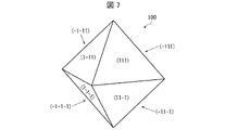
- the surface of the quantum dot 100 is, for example, (a) the quadrangular (100) plane, (-100) plane, (010) plane, (0-10) plane, (001) plane, and (00-1) plane shown in FIG. ) plane, and (b) the hexagonal (111) plane, (-111) plane, (1-11) plane, (-1-11) plane, (11-1) plane, (-11 -1), (1-1-1), and (-1-1-1) 14 planes.
- the ideal shape of the quantum dot 100 is a tetradecahedron obtained by cutting each vertex of a regular octahedron into squares.
- FIG. 3 is a diagram showing a plane equivalent to the (111) plane among the crystal planes of the quantum dot 100.
- the (111) plane and planes equivalent to the (111) plane are hatched.
- planes equivalent to the (111) plane are the (-111) plane, (1-11) plane, (-1-11) plane, (11-1) plane, (-11 -1) plane, (1-1-1) plane, and (-1-1-1) plane.
- FIG. 4 is a diagram showing a plane equivalent to the (100) plane among the crystal planes of the quantum dot 100. As shown in FIG. In FIG. 4, the (100) plane and planes equivalent to the (100) plane are hatched.
- the planes equivalent to the (100) plane are the (-100) plane, (010) plane, (0-10) plane, (001) plane, and (00-1) plane. be.
- the (111) equivalent plane and the (100) equivalent plane in the sphalerite-type crystal system are polar planes.
- a polar plane is a crystal plane in which the valences of cations and anions exposed on the surface are biased.
- the polar surface is a surface that is positively charged due to the presence of more cations than anions on the surface, and that can strongly bind to a negatively charged polar ligand.
- non-polar planes are crystal planes in which the valences of exposed cations and anions are in balance.
- a non-polar surface is a surface that is electrically neutral, has no charge, and can strongly bind to a non-polar ligand.
- the method for identifying whether it is a polar face or a non-polar face can be specified by the method described in "(Quantum dot crystal face analysis method)" below.
- the surface of the quantum dot 100 is a polar plane, the surface of the quantum dot 100 can be protected (surface protection) using the polar ligand 2, as shown in FIG.
- a polar ligand 2 can coordinate to a polar face via a lone pair of electrons.
- a quantum dot light-emitting device was manufactured using a quantum dot in which 50% of the surface area was a polar plane and only polar ligands were coordinated. and measured the endurance time. As a result, it was found that the luminance half life time was about 6400 hours at a driving luminance of 1000 cd/m 2 .
- 50% of the polar faces means that the remaining 50% of the faces are non-polar faces. These non-polar faces are weakly bound to polar ligands, and polar ligands tend to detach from these non-polar faces.
- the non-radiative recombination probability can be expressed as 0.5pa (because the nonpolar plane is 50%).
- 100% of the surface area of p a is a non-polar plane, and when quantum dots with only polar ligands coordinated are used, the polar ligands deviate from the non-polar planes to form defect levels. and the probability of causing non-radiative recombination of excitons via this defect level is pa (0 ⁇ p a ⁇ 1).
- the non-radiative recombination gives thermal energy to the quantum dots and deactivates the quantum dots with a certain probability. If the probability of QD deactivation due to non-radiative recombination is p b (0 ⁇ p b ⁇ 1), the probability of QD deactivation per average time taken for one exciton recombination is 0.5 p a p b .
- the proportions of polar planes are 70%, 80%, and 90%, respectively, the proportions c of non-polar planes are 0.3, 0.2, and 0.1, respectively.
- the luminance half life time t 1/2 is 10667 hours, 16000 hours and 32000 hours, respectively. Assuming that the light-emitting device containing the quantum dots of the present application is used for a television display, and the television viewing time per day is 3 hours, these values are 9.74 years, 14.6 years, and 29.2 years. number of years.
- Luminance half-life time at 1000 cd/m 2 for the self-luminous element 5 using the quantum dots 100 in which the ratio of the polar planes to the surface of the quantum dots 100 (hereinafter referred to as the “area ratio of the polar planes”) is 70% More than 10,000 hours of results are expected.
- a brightness half life of 10,000 hours or more at 1000 cd/m 2 corresponds to about 10 years of service life of the display.
- a service life of 10 years is generally sufficient for commercial production.
- the self-luminous element 5 that emits blue light using the quantum dots 100 having a polar surface area ratio of 80% or more is expected to have a useful life equivalent to about 15 years of the display.
- the self-luminous element 5 that emits blue light using the quantum dots 100 having a polar surface area ratio of 90% or more is expected to have a useful life equivalent to about 30 years of the display.
- the surface of the quantum dot 100 can be sufficiently protected (surface protected) using only the polar ligand 2.
- the surface of the quantum dot 100 according to Embodiment 1 may be a polar surface with an area ratio of 70% or more, preferably 80% or more is a polar surface, and 90% or more is a polar surface. more preferred. Also, ideally, the surface of the quantum dot 100 contains only polar planes.
- the protective effect of the quantum dot surface by the polar ligand or the neutral ligand is evaluated by evaluating the binding energy of the polar ligand on the polar plane and the non-polar plane of the quantum dot surface.
- the surface of the quantum dot 100 is made of CdSe and the polar ligand 2 is a carboxylic acid-based ligand
- the binding energy per 1 mol of the polar ligand 2 to the surface of the quantum dot 100 was calculated. The calculation was based on the density functional theory (DFT).
- the binding energy for the (100) equivalent plane and the (111) equivalent plane, which are polar planes is about 240 kcal/mol
- the binding energy for the (110) equivalent plane, which is a nonpolar plane is about 16 kcal/mol. is.
- the area ratio of the polar plane is 70% or more. Therefore, the area ratio of the nonpolar plane in the quantum dot 100 is small.
- the polar ligand 2 bound to the polar face of the quantum dot 100 blocks access of other quantum dots 100 to the non-polar face of the quantum dot 100 . As a result, even if the quantum dot 100 is surface-protected only with the polar ligand 2, the non-polar surface of the quantum dot 100 is less likely to deteriorate.
- the method for manufacturing the light-emitting layer 54 according to Embodiment 1 does not require a process of mixing a polar ligand and a neutral ligand or a process of exchanging ligands. Therefore, the light-emitting layer 54 according to Embodiment 1 has high manufacturing efficiency. Moreover, the ligand used for the surface protection of the quantum dot 100 can be made into a single species.
- the polar ligand 2 may be organic, for example, selected from the group consisting of organic polar ligands containing one or more of a terminal thiol group, an alkoxyl group, a carboxyl group, a phosphonic acid group, and a phosphinic acid group. contains at least one A ligand containing one or more thiol groups at its terminal partly contains a structure represented by the following structural formula (1) or the following structural formula (2) in an ionized state. A ligand containing an alkoxyl group at its terminal partly contains a structure represented by the following structural formula (3) in an ionized state. A ligand containing a terminal carboxyl group partially contains a structure represented by the following structural formula (4) in an ionized state.
- a ligand containing a phosphonic acid group at its terminal partly contains a structure represented by the following structural formula (5) or the following structural formula (6) in an ionized state.
- a ligand containing a phosphinic acid group at its terminal partly contains a structure represented by the following structural formula (7) in an ionized state.
- C represents a carbon atom
- O represents an oxygen atom
- O - represents an oxide ion
- S represents a sulfur atom
- S - represents a sulfide ion
- P represents a phosphorus atom
- R 1 and R 2 each independently represent a hydrogen atom, an alkyl group, an aryl group, an alkoxyl group, or an unsaturated hydrocarbon group.
- the polar ligand 2 is preferably organic.
- Organic ligands can have a long chain molecular structure, unlike inorganic ligands. Therefore, the organic ligand tends to keep the distance between the quantum dots 100 large, so that the dispersibility and storage stability of the quantum dots 100 in the solution can be improved.
- the polar ligands 2 may be inorganic, for example in the ionized state, with the ionic formulas Cl ⁇ , Br ⁇ , I ⁇ , SCN ⁇ , CN ⁇ , OH ⁇ , SH ⁇ , SeH ⁇ , TeH ⁇ , Se 2 ⁇ , S 2 ⁇ , Te 2 ⁇ , Sn 2 S 6 4 ⁇ , Sn 2 Se 6 4 ⁇ , In 2 Se 4 2 ⁇ , In 2 Te 4 2 ⁇ , Ga 2 Se 4 2 ⁇ , Sb 2 Se 4 2 ⁇ , Sb 2 Te 4 2- .
- the polar ligand 2 is inorganic.
- Organic bonds (such as C—H and C—C) are susceptible to cleavage by heat and light.
- the polar ligand 2 is inorganic, it does not contain an organic bond and is therefore difficult to decompose.
- the polar ligand 2 is Se 2- , S 2- or Te 2- . This is because Se 2 ⁇ , S 2 ⁇ , and Te 2 ⁇ do not contain chemical bonds and are not decomposed, and since they have negative valences of two, they can be strongly bonded to the polar plane of the quantum dots 100. It is from.
- the quantum dots 100 do not aggregate in the solution, (2) It is necessary not to hinder the flow of the solvent.
- the ligands coordinated to the surfaces of the quantum dots 100 should have a high density with respect to the volume of the quantum dots 100 in the applied colloidal solution.
- the inertia of the quantum dots 100 in the applied colloidal solution should be small with respect to the viscosity of the solvent of the applied colloidal solution.
- the smaller the size of the quantum dots 100 in the colloidal solution the easier it is for both of the above (1) and (2) to be satisfied.
- the size of the quantum dots 100 is preferably 10 nm or less. In other words, if the thickness is 10 nm or less, a uniform film can be formed when the light-emitting layer 54 (see FIG. 1) of the light-emitting element is formed by coating or the like.
- the size of the quantum dot 100 may be a nominal value, a design value, or a measured value.
- the size of the quantum dots 100 is, for example, a value obtained by measuring the particle size of the quantum dots 100 multiple times using a transmission electron microscope (TEM) or the like and averaging the values.
- TEM transmission electron microscope
- Methods for manufacturing the quantum dots 100 include, for example, a heating method, hot injection, microwave assist method, and continuous flow method. Each of these manufacturing methods will be described.
- the heating method is a method of synthesizing each layer of the quantum dots 100 by mixing materials in an organic solvent and heating to thermally decompose and react the materials.
- TOP trioctylphosphine
- TOPO trioctylphosphine oxide
- dimethylcadmium is used as a group II raw material
- a desired element such as S, Se, Te, etc.
- a complex or an organometallic compound combined with a methyl group, an ethyl group, or the like is used.
- Group II and Group VI raw materials are mixed in an organic solvent, heated to about 300° C. to pyrolyze the raw materials, and by maintaining a high degree of supersaturation of Group II and Group VI elements in the organic solvent, Group II-VI compounds are produced.
- Each layer of quantum dots 100 can be synthesized by facilitating the reaction to
- Hot injection is a method of rapidly injecting a raw material into a heated organic solvent and utilizing supersaturation in the vicinity of the injection region to produce uniform crystal growth nuclei at high density.
- the raw material to be used is TOP or T-TOPO as an organic solvent, heated to about 300 ° C., and rapidly injected into the organic solvent with group II and group VI raw materials.
- the degree of supersaturation is rapidly increased to form uniform crystal growth nuclei at high density. Since the high supersaturation is localized in the vicinity of the injection region, the material consumed in the growth of the growth nuclei is supplied from the surrounding low supersaturation region by diffusion at any time due to the concentration gradient, and the growth of the quantum dots continues.
- This approach uses alkylphosphine and trioctylphosphine or alkylphosphine oxides such as trioctylphosphine oxide as surfactants or ligands that prevent quantum dot aggregation due to high nucleation density, and long-chain compounds such as oleic acid. Carboxylic acids, long-chain amines such as oleylamine are added.
- the microwave-assisted method is a method of selectively heating the growth material using microwaves. Since this method is selective in heating, the reaction is well controllable, and the temperature can be raised to the temperature range required for the reaction in a short period of time.
- quantum dots can be synthesized easily and even in the atmosphere. Microwaves are selectively resonantly absorbed by polarized molecules. For example, if a chalcogenide that matches the wavelength of microwaves is used as a raw material, it is possible to selectively heat the raw material and control the growth of quantum dots. Because of this feature, the raw material must have polarization, and a raw material different from that used in the first and second methods is used.
- An example of raw materials is a mixed solution of cadmium stearate, an alkane solvent, and a Group VI powder.
- the continuous flow method is a method of causing a nucleation reaction and a growth reaction to occur in different reactors by reacting the raw materials while flowing an organic solvent mixed with the raw materials. Since the nucleation reaction and the growth reaction are caused in different reactors, suitable temperature gradients can be precisely set and each reaction can be precisely controlled. This technique is suitable for mass production in that the control of crystal growth is relatively easy. Quantum dots 100 can be grown either in an organic solution or in a vapor phase containing vapors of an organic solution, both in the continuous flow method and as described in the previous three manufacturing methods.
- the organic solvent is mixed with the group II and group VI raw materials, the raw materials are moved along the flow of the liquid phase or the gas phase, and the nucleation stage serving as the starting point for the growth of the quantum dots 100, and the crystal growth
- the nucleation stage serving as the starting point for the growth of the quantum dots 100, and the crystal growth
- the quantum dots 100 In order to synthesize the quantum dots 100, it is necessary to control the synthesis conditions when synthesizing each layer of the quantum dots 100. Specifically, it is necessary to control the conditions for synthesizing each layer of the quantum dots 100 so that the surface of the quantum dots 100 has a shape terminated only by the (111) equivalent plane and the (100) equivalent plane as shown in FIG. be.
- the (111) equivalent plane is I know it will show up. This is because the reduction of the group V or group VI raw material relatively increases the number of dangling orbitals on the (111) equivalent plane, which has a high areal density of bonding orbitals.
- the (111) equivalent plane and the (100) equivalent plane include 14 planes.
- a quantum dot 100 is obtained.
- heat may be applied for heat treatment.
- defects on the surface of the outermost layer of the quantum dots 100 can be reduced by stopping the reaction and performing heat treatment.
- the ligands can be replaced by adding a sufficient amount of the polar ligand 2 after the quantum dots 100 are produced and heating at 150°C for 20 minutes.
- Quantum dots 100 having a polar plane to which polar ligands 2 are coordinated can also be obtained by adding polar ligands 2 at the final stage of crystal growth of quantum dots 100 or at the time of shell formation.
- the particle diameter of the quantum dots 100 may be 3 nm or more and 40 nm or less, excluding the polar ligand 2.
- Quantum dot crystal face analysis method Next, a method for analyzing crystal planes of the quantum dots 100 will be described. Simple, conventional X-ray diffraction (XRD) measuring device, Energy Dispersive X-ray Spectroscopy (EDS) measuring device, X-ray Photoelectron Spectroscopy
- XRD X-ray diffraction
- EDS Energy Dispersive X-ray Spectroscopy
- TEM transmission electron microscope
- the crystal system of quantum dots 100 can be measured by X-ray diffraction. With a thickness of about 20 nm, diffraction peaks from each crystal face of the quantum dot 100 can be detected with sufficient accuracy by a general X-ray powder diffraction method. Therefore, the crystal system of the quantum dot 100 can be measured by collating the obtained spectral shape with a database or past literature values.
- composition analysis of the quantum dots 100 can be determined by EDS or XPS. This is because, depending on the composition of the quantum dot 100, peaks peculiar to the elements contained in the composition and their bonding states appear in the spectroscopic results.
- the crystal plane spacing and crystal plane index of the quantum dots 100 can be calculated based on the composition and crystal system of the quantum dots 100. By using these values and combining them with TEM observation, it is possible to measure the plane index and ratio of the surface of the nanoparticles. Ultimately, the area ratio of the polar plane to the surface of the quantum dot 100 can be calculated based on the composition, crystal system, and crystal plane index.
- the light-emitting layer 54 has a uniform structure regardless of location with respect to the shape and surface index of the quantum dots 100, and the types and ratios of ligands. Therefore, analysis results performed on a portion of the light-emitting layer 54 may be applied to the entire light-emitting layer 54 .
- the object to be analyzed by the above analysis method includes the lower layer of the outermost layer.
- the crystal system of the outermost layer follows the crystal system of the underlying layer. Therefore, regardless of the thickness of the outermost layer of the quantum dots 100 , the crystal system and crystal indices derived based on the above analysis method can be regarded as the crystal system and crystal indices of the outermost layer of the quantum dots 100 .
- the calculated polar plane area ratio is 90% or more and less than 100% due to analysis accuracy, measurement limit, impurities, etc. tend to be Therefore, if the calculated area ratio of the polar plane is 90% or more, it is highly probable that the light-emitting layer 54 has quantum dots in which 100% of the surface is a polar plane. Therefore, if the area ratio of the polar plane in the analysis result is 90% or more, it is considered that the light-emitting layer 54 contains quantum dots in which 100% of the surface is a polar plane.
- the polar plane should occupy 70% or more of the surface of the quantum dot 100.
- the calculated polar plane area ratio tends to be 60% or more and 80% or less. Therefore, when the calculated area ratio of the polar plane is 60%, it is highly probable that the entire light-emitting layer 54 includes the quantum dots 100 having the area ratio of the polar plane of 70% or more.
- 70% or more of the surface of the quantum dot 100 is a polar plane, the surface of the quantum dot 100 can be sufficiently protected (surface protected) using only the polar ligand 2 . Therefore, when the area ratio of the polar plane in the analysis results is 60% or more, at least part of the quantum dots 100 contained in the light-emitting layer 54 are considered to be sufficiently surface-protected by the polar ligand 2 alone.
- the analysis method of the area ratio of non-polar planes can also be specified by the same method as above. If the calculated area ratio of non-polar planes is 90% or more, it is considered that the light-emitting layer 54 contains quantum dots 100 in which 100% of the surface is non-polar planes.
- Ligand analysis method Functional groups of ligands, including polar ligands 2 and neutral ligands 3 described below, can be determined using a mass spectrometer. If the ligand is organic, the ligand is ionized and cleaved into multiple fragments and the m/z value (mass/charge) of each fragment and the intensity ratio in the mass spectrum are obtained. Then, based on the m/z value and intensity ratio, a database can be referred to determine the structural formula and functional group of the ligand.
- the compositional formula of the ligand can be determined using a mass spectrometer or an EDS measurement device. Also, as noted above, analysis results performed on a portion of light-emitting layer 54 may be applied to light-emitting layer 54 as a whole.
- the light-emitting layer 54 is analyzed as described above to identify compounds that can function as ligands contained in the light-emitting layer 54 . Even if only the polar ligand 2 (or only the neutral ligand 3) was used as the ligand in the light-emitting layer 54 during manufacturing, the polar ligand 2 (or the neutral ligand 3) was identified due to analytical accuracy and measurement limits. It tends to be less than 100% of the compound. Therefore, if the polar ligand 2 (or the neutral ligand 3) accounts for 90% or more of the specified compound, 100% of the ligands contained in the light-emitting layer 54 are the polar ligand 2 (or the neutral ligand 3). It is considered highly probable that it is ligand 3).
- FIG. 8 is a cross-sectional view schematically showing a solar cell 6 having a photoelectric conversion layer 57 containing quantum dots 100 according to the first embodiment.
- the quantum dot 100 according to Embodiment 1 is not limited to the above.
- the surface of quantum dot 100 may, for example, comprise six (100) equivalent planes as shown in FIG. 6, in which case the ideal shape of quantum dot 100 is a cuboid.
- the surface of the quantum dot 100 may include, for example, eight (111) equivalent planes, as shown in FIG. 7, in which case the ideal shape of the quantum dot 100 is a regular octahedron.
- a hexahedral quantum dot 100 as shown in FIG. 6 can be produced by increasing the reaction temperature.
- the quantum dots 100 are made of CdSe, they are grown at 275 degrees Celsius or higher. Elevated temperatures increase the rate of ligand desorption and re-adsorption at crystal surfaces, resulting in a predominance of atomic deposition on crystal faces with high surface energies. In other words, atoms are preferentially deposited on the (111) equivalent surface having a high density of dangling bonds. As a result, the surface of the quantum dot 100 is composed of the (100) equivalent plane.
- the quantum dots 100 when forming a film by coating using a colloidal solution in which the quantum dots 100 are dispersed, in order to achieve a uniform thickness everywhere and reduce surface unevenness, (1) the quantum dots in the solution It is necessary that 100 does not agglomerate and (2) does not impede the flow of the solvent. In order to satisfy (2), it is preferable that the quantum dots 100 have a shape that is easy to roll, that is, a shape close to a sphere. Furthermore, in order to reduce the driving voltage of the self-luminous element 5, it is necessary that the gap between the quantum dots 100 in the light-emitting layer 54 is small.
- the quantum dots 100 have a shape that facilitates filling in a small gap, that is, a shape close to a sphere. Therefore, the shape of the quantum dot 100 is preferably an octahedron rather than a hexahedron, and more preferably a tetradecahedron than an octahedron.
- the first embodiment can be applied to the solar cell 6.
- Solar cell 6 includes anode 51 , hole injection layer 52 , hole transport layer 53 , photoelectric conversion layer 57 (quantum dot layer), electron transport layer 55 and cathode 56 .
- the photoelectric conversion layer 57 includes the quantum dots 100 and the polar ligands 2 according to the first embodiment.
- the self-luminous element 5 (see FIG. 1) according to the second embodiment is only in that the light-emitting layer 54 includes the quantum dots 200 according to the second embodiment instead of the quantum dots 100 according to the first embodiment. , is different from the self-luminous element 5 according to the first embodiment.
- FIG. 9 is a perspective view showing an example structure of the quantum dot 200 according to the second embodiment.
- the quantum dot 200 according to Embodiment 2 has a sodium chloride type crystal system.
- the quantum dot 200 preferably contains at least one selected from the group containing materials that can spontaneously assume a sodium chloride type crystal system.
- the material is, for example, a IV-VI group compound such as PbTe, PbSe, PbS.
- a group IV-VI compound means a compound containing a group IV element and a group VI element.
- group IV elements may include group 4 elements and group 14 elements.
- the bandgap of the core is preferably smaller than the bandgap of the shell, as in Embodiment 1 described above.
- the quantum dot 200 is a polyhedral crystal having a plurality of crystal planes, the surfaces of which are mainly polar planes.
- the surfaces of the quantum dots 200 are, for example, the triangular (111) plane, (-111) plane, (1-11) plane, (-1-11) plane, (11-1) plane, (-11 -1) plane, (1-1-1) plane, and (-1-1-1) plane. These eight faces are (111) equivalent faces.
- the ideal shape of quantum dot 200 is a regular octahedron.
- the (111) equivalent plane in the sodium chloride type crystal is a polar plane.
- the surface of the quantum dot 200 according to Embodiment 2 may be a polar surface with an area ratio of 70% or more, preferably 80% or more, as in Embodiment 1 described above, and preferably 90% or more. is more preferably a polar face. Also, ideally, the surface of the quantum dot 200 contains only polar planes.
- the light-emitting layer 54 has quantum dots in which 100% of the surface is a polar plane. Dot 200 is considered to be included.
- the manufacturing method of the quantum dot 200 according to the second embodiment includes, for example, a heating method, a hot injection method, a microwave assist method, and a continuous flow method, as in the first embodiment described above.
- the octahedral quantum dot 100 as shown in FIG. 7 uses, in addition to the production method described in Non-Patent Document 1, a polar ligand that preferentially binds to the polar plane during synthesis (for example, a ligand containing a thiol group). can be produced by lowering the reaction temperature.
- a polar ligand that preferentially binds to the polar plane during synthesis for example, a ligand containing a thiol group.
- crystal growth is performed at about 110 degrees Celsius.
- the second embodiment can also be applied to solar cells as in the first embodiment.
- the self-luminous element 5 (see FIG. 1) according to the third embodiment is only in that the light emitting layer 54 includes the quantum dots 300 according to the third embodiment instead of the quantum dots 100 according to the first embodiment. , is different from the self-luminous element 5 according to the first embodiment.
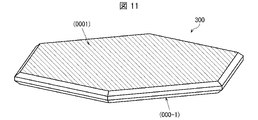
- FIG. 10 is a perspective view showing an example structure of the quantum dot 300 according to the third embodiment.
- FIG. 11 is a diagram showing the plane orientation of each crystal plane of the quantum dot 300 shown in FIG.
- the quantum dot 300 according to Embodiment 3 has a wurtzite crystal system.
- Quantum dot 300 preferably includes at least one selected from the group including materials capable of spontaneously adopting a wurtzite crystal system.
- the material is, for example, a II-VI group compound such as ZnS, CdSe, ZnSe.
- the group II-VI compound can also take a zincblende crystal system.
- the core bandgap is preferably smaller than the shell bandgap, as in Embodiment 1 described above.
- the quantum dot 300 is a polyhedral crystal having a plurality of crystal planes, the surfaces of which are mainly polar planes.
- the quantum dot 300 has, for example, a flat plate shape thin in the [0001] direction, which includes the (0001) plane and the (000-1) plane of the hexagon shown in FIG. 11 as the top and bottom surfaces.
- FIG. 11 is a diagram showing a plane equivalent to (0001) in the crystal plane of the quantum dot 300.
- the (0001) plane and planes equivalent to the (0001) plane are hatched.
- the plane equivalent to the (0001) plane is the (000-1) plane opposite to the (0001) plane.
- the (0001) equivalent plane and (1-101) equivalent plane in wurtzite crystals are polar planes.
- the (1-101) equivalent plane is the (1-101) plane, (01-11) plane, (-1011) plane, (-1101) plane, (0-111) plane, (10-11 ) plane, (1-10-1) plane, (01-1-1) plane, (-101-1) plane, (-110-1) plane, (0-11-1) plane, (10-1 ⁇ 1) plane, 12 planes.
- the surface of the quantum dot 300 according to Embodiment 3 may be a polar surface with an area ratio of 70% or more, preferably 80% or more, as in Embodiment 1 described above, and preferably 90% or more. is more preferably a polar face. Also, it is ideal that the quantum dot 300 has a flat plate shape.
- the light-emitting layer 54 has quantum dots in which 100% of the surface is a polar plane. Dot 300 is considered to be included.
- a plane between the top and bottom surfaces of the quantum dot 300 may include a non-polar plane, for example, a (1-100) equivalent plane.
- the (1-100) equivalent plane is the (1-100) plane, (01-10) plane, (-1010) plane, (-1100) plane, (0-110) plane, (10-10 ) face.
- the plane between the top and bottom surfaces of the quantum dot 300 preferably includes a polar plane, eg, a (1-101) equivalent plane that is tilted with respect to the (0001) equivalent plane.
- the planes between the top and bottom surfaces of quantum dots 300 may include non-polar and/or polar planes.
- the quantum dot 300 has a thin plate shape in the [0001] direction because the proportion of the area of the (0001) equivalent plane on the surface of the quantum dot 300 is large. Therefore, the direction of recombination of excitons in the quantum dot 300 is mainly the direction substantially perpendicular to the [0001] direction. As a result, light emitted by recombination of excitons is strongly emitted in a direction substantially parallel to the [0001] direction.
- the quantum dots 300 tend to deposit due to their own weight such that one of the (0001) equivalent planes of the quantum dots 300 is positioned on the top side or the bottom side of the light-emitting layer 54 .
- the light-emitting layer 54 in the self-light-emitting element 5 mainly emits light in a direction substantially orthogonal to the top surface and bottom surface of the light-emitting layer 54 . Therefore, since the incident angle is small, the radiated light is less likely to be reflected at the boundary surface of the self-luminous element 5, and the attenuation of the light inside the self-luminous element 5 is reduced. This improves the efficiency of extracting light from the self-luminous element 5 .
- the method of manufacturing the quantum dots 300 according to the third embodiment includes, for example, a heating method, a hot injection method, a microwave assisted method, and a continuous flow method, as in the first embodiment described above.
- FIG. 12 and 13 are diagrams each showing an example manufacturing method of the quantum dot 300 shown in FIG.
- a flat plate-shaped wurtzite quantum dot 300 as shown in FIG. 10 can be manufactured by forming a material having a wurtzite crystal system into a sheet and substituting ions as necessary.
- the quantum dots 300 are composed of CdSe
- the nanosheet-like complexes of CdCl 2 are first formed by adding oleylamine (shown as OA in FIG. 12) to CdCl 2 .
- CdCl2 is a material that normally has a wurtzite crystal system.
- the Se melted octylamine solution is mixed with the aforementioned CdCl 2 complex and reacted at 100 degrees Celsius for 24 hours.
- two chloride ions Cl ⁇ are replaced by one selenide ion Se ⁇ to form a CdSe nanosheet complex.
- the CdSe thus formed has a tabular and wurtzite crystal system.
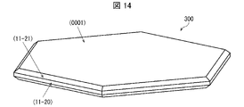
- FIG. 14 is a perspective view showing the structure of a modification of the quantum dot 300 according to Embodiment 3.
- FIG. 14 is a perspective view showing the structure of a modification of the quantum dot 300 according to Embodiment 3.
- the plane between the top and bottom surfaces of the quantum dot 300 may include, for example, the (11-20) plane and a plane equivalent to the (11-20) plane as shown in FIG. 14 as non-polar planes.
- the planes between the top and bottom surfaces of the quantum dot 300 may include, for example, the (11-21) plane and planes equivalent to the (11-21) as polar planes.
- the planes equivalent to (11-20) are the (-2110) plane, (1-210) plane, (-1-120) plane, (2-1-10) plane, and (-12-10) plane, is.
- the planes equivalent to (11-21) are the (-2111) plane, (1-211) plane, (-1-121) plane, (2-1-11) plane, (-12-11), (- 2111) plane, (11-2-1) plane, (1-21-1) plane, (-1-12-1) plane, (2-1-1-1) plane, and (-12-1- 1) It is a face.
- the (11-20) plane and a plane equivalent to the (11-20) plane are collectively referred to as the (11-20) equivalent plane, and
- the faces are collectively referred to as (11-21) equivalent faces.
- the third embodiment can also be applied to solar cells as in the first embodiment.
- the light-emitting layer 54 (see FIG. 1) according to Embodiment 4 includes the quantum dots 400 and neutral ligands 3 according to Embodiment 4 instead of the quantum dots 100 and polar ligands 2 according to Embodiment 1 described above. It differs from the self-luminous element 5 according to the first embodiment described above only in this point.
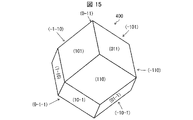
- FIG. 15 is a perspective view showing an example structure of the quantum dot 400 according to the fourth embodiment.
- FIG. 16 is a schematic diagram schematically showing the surface of the quantum dot 400 shown in FIG. 15 and the neutral ligand 3 protecting the surface.
- Quantum dot 400 has a zinc blende crystal system.
- Quantum dot 400 preferably includes at least one selected from the group including materials capable of spontaneously adopting a zinc blende crystal system.
- materials are, for example, II-VI compounds such as ZnS, CdSe, ZnSe and III-V compounds such as InP.
- the core bandgap is preferably smaller than the shell bandgap, as in Embodiment 1 described above.
- the quantum dot 400 is a polyhedral crystal having multiple crystal planes, the surfaces of which are mainly non-polar planes.
- the surface of the quantum dot 400 is, for example, the rhombic (110) plane, (011) plane, (101) plane, (1-10) plane, (01-1) plane, (-101) plane, (-101) plane, ( -110) plane, (0-11) plane, (10-1) plane, (-1-10) plane, (0-1-1) plane, and (-10-1) plane.
- the ideal shape of quantum dot 400 is a dodecahedron.
- planes equivalent to the (110) plane are the (011) plane, (101) plane, (1-10) plane, (01-1) plane, ( ⁇ 101) plane, ( ⁇ 110) plane, (0-11) plane, (10-1) plane, ( ⁇ 1-10) plane, (0-1-1) plane, and ( ⁇ 10-1) plane.
- the (110) equivalent plane in the sphalerite-type crystal system is a non-polar plane.
- the surface of the quantum dot 400 is a non-polar plane, the surface of the quantum dot 400 can be sufficiently protected (surface protected) using only the neutral ligand 3, as shown in FIG. A neutral ligand 3 can bind to the non-polar surface via a lone pair of electrons 3a.
- the surface of the quantum dot 400 according to Embodiment 4 is a non-polar surface, for the same reason as in Embodiment 1 described above, the surface of the quantum dot 400 is sufficiently covered using only the neutral ligand 3. Can be protected (surface protection).
- the surface of the quantum dot 400 according to Embodiment 4 may be a non-polar surface with an area ratio of 70% or more, and preferably 80% or more is a non-polar surface, contrary to the above-described Embodiment 1. , 90% or more of which are non-polar surfaces. Also, ideally, the surface of quantum dot 400 includes only non-polar planes.
- the area ratio of the nonpolar plane calculated in the result of the crystal plane analysis of the quantum dots 400 is 60% or more, at least part of the quantum dots 400 included in the light emitting layer 54 It is believed that neutral ligand 3 alone provides sufficient surface protection. Moreover, if it is 90% or more, it is considered that the light-emitting layer 54 contains the quantum dots 400 in which 100% of the surface is a non-polar plane.
- a non-polar surface has a smaller surface charge and a smaller concentration of dangling bonds than a polar surface. For this reason, nonpolar surfaces tend to have relatively low reactivity, and when ligands are desorbed from the surface of quantum dots, nonpolar surfaces tend to react relatively poorly with impurities and the like. Therefore, since the quantum dots 400 according to the fourth embodiment are less likely to deteriorate, the reliability of the light-emitting layer 54 and the self-light-emitting element 5 can be improved.
- the neutral ligand 3 is organic and includes, for example, at least one selected from the group consisting of organic neutral ligands containing one or more phosphine groups, phosphine oxide groups, and amine groups at the ends.
- a ligand containing a phosphine group at its terminal partly includes a structure represented by the following structural formula (8) or the following structural formula (9).
- a ligand containing a phosphine oxide group at its terminal partly includes a structure represented by the following structural formula (10).
- a ligand containing an amine group at its terminal partly includes a structure represented by any one of the following structural formulas (11) to (15).
- H represents a hydrogen atom
- N represents a nitrogen atom
- O represents an oxygen atom
- P represents a phosphorus atom
- R 1 , R 2 and R 3 each independently represents a hydrogen atom, an alkyl group, an aryl group, an alkoxyl group, or an unsaturated hydrocarbon group.
- Methods for manufacturing the quantum dots 400 include, for example, a heating method, a hot injection method, a microwave assist method, and a continuous flow method, as in the first embodiment described above.
- a dodecahedral quantum dot as shown in FIG. 15 can be produced using a neutral ligand that preferentially binds to the non-polar face during synthesis of the outermost layer.
- a neutral ligand that preferentially binds to the non-polar face during synthesis of the outermost layer.
- the quantum dots 400 are made of CdSe
- a large amount of neutral ligand is added and the crystal is grown at a reaction temperature of about 250 degrees.
- Neutral ligands are preferably amine-based ligands. Amine-based ligands bind strongly to the (110) equivalent face of CdSe and weakly or not to other faces. As a result, crystal growth progresses on planes other than the (110) equivalent plane, and the surface of the quantum dot 400 is composed of the (110) equivalent plane.
- the fourth embodiment can also be applied to solar cells as in the first embodiment.
- the light-emitting layer 54 (see FIG. 1) according to Embodiment 5 includes quantum dots 500 and neutral ligands 3 according to Embodiment 5 instead of the quantum dots 100 and polar ligands 2 according to Embodiment 1 described above. It differs from the self-luminous element 5 according to the first embodiment described above only in this respect.
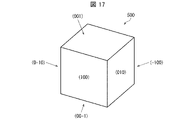
- FIG. 17 is a perspective view showing an example structure of a quantum dot 500 according to the fifth embodiment.
- the quantum dot 500 according to Embodiment 5 has a sodium chloride type crystal system.
- the quantum dot 200 preferably contains at least one selected from the group containing materials that can spontaneously assume a sodium chloride type crystal system.
- the material is, for example, a IV-VI group compound such as PbTe, PbSe, PbS.
- the core bandgap is preferably smaller than the shell bandgap, as in Embodiment 1 described above.
- the quantum dot 500 is a polyhedral crystal having a plurality of crystal planes, the surfaces of which are mainly non-polar planes.
- the surface of the quantum dot 500 is, for example, the quadrangular (100) equivalent plane, ( ⁇ 100) plane, (010) plane, (0-10) plane, (001) plane, and (00-1) plane shown in FIG. including six sides of These six faces are (100) equivalent faces.
- the ideal shape of quantum dot 500 is a cuboid.
- the (100) equivalent plane in the sodium chloride type crystal system is a non-polar plane.
- the surface of the quantum dot 500 according to Embodiment 5 may be a nonpolar surface with an area ratio of 70% or more, preferably 80% or more, as in Embodiment 4 described above. % or more are non-polar planes. Also, ideally, the surface of quantum dot 500 includes only non-polar planes.
- the area ratio of the non-polar planes calculated in the crystal plane analysis results of the quantum dots 500 is 90% or more, 100% of the surface of the light-emitting layer 54 is non-polar planes. is believed to contain quantum dots 500 that are
- the method of manufacturing the quantum dots 500 according to the fifth embodiment includes, for example, a heating method, a hot injection method, a microwave assisted method, and a continuous flow method, as in the first embodiment described above.
- a hexahedral quantum dot 500 as shown in FIG. 17 uses a neutral ligand (amine-based ligand) that preferentially binds to a non-polar surface when synthesizing the outermost layer, in addition to the manufacturing method described in Non-Patent Document 1. can be produced by lowering the reaction temperature. For example, when the quantum dots 100 are made of PbS, crystal growth is performed at about 110 degrees Celsius.
- the fifth embodiment can also be applied to solar cells as in the first embodiment.
- the light-emitting layer 54 is the quantum dots 600 and the quantum dots 600 according to the sixth embodiment instead of the quantum dots 100 and the polar ligands 2 according to the first embodiment It differs from the self-luminous element 5 according to the first embodiment described above only in that the neutral ligand 3 is included.
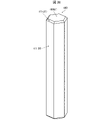
- FIG. 18 is a perspective view showing the structure of a quantum dot 600 according to Embodiment 6.
- FIG. 19 is a diagram showing the plane orientation of each crystal plane of the quantum dot 600 shown in FIG.
- the quantum dot 600 according to Embodiment 6 has a wurtzite crystal system.
- Quantum dot 600 preferably includes at least one selected from the group including materials capable of spontaneously adopting a wurtzite crystal system.
- the material is, for example, a II-VI group compound such as ZnS, CdSe, ZnSe.
- the group II-VI compound can also take a zincblende crystal system.
- the quantum dot 600 is a polyhedral crystal having a plurality of crystal planes, the surfaces of which are mainly polar planes.
- Quantum dots 600 are, for example, rectangular (1-100) planes, (0-110) planes, (-1010) planes, (-1100) planes, (01-10) planes, and (10-10) planes shown in FIG. ) in the direction of [0001] including 6 faces as side faces.
- Bar shapes include hexagonal prism shapes and shapes obtained by truncating one or more corners of hexagonal prisms.
- FIG. 19 is a diagram showing a plane equivalent to the (1-100) plane among the crystal planes of the quantum dot 600.
- the (1-100) plane and planes equivalent to the (1-100) plane are hatched.
- the planes equivalent to the (1-100) plane are the (0-110) plane, (-1010) plane, (-1100) plane, (01-10) plane, and (10 -10).
- the (-1100) equivalent plane in the wurtzite crystal is a non-polar plane.
- the surface of the quantum dot 600 according to Embodiment 6 may be a non-polar surface with an area ratio of 70% or more, preferably 80% or more, as in Embodiment 4 described above. % or more are non-polar planes. Also, ideally, the surface of quantum dot 600 includes only non-polar planes.
- the area ratio of the nonpolar plane calculated in the result of the crystal plane analysis of the quantum dots 600 is 90% or more, 100% of the surface of the quantum dots 600 is in the light emitting layer 54. It is believed to contain quantum dots 600, which are non-polar planes.
- Quantum dot 600 may have a polar surface between one of its sides and a surface between the other of its sides, such as (0001) equivalence and/or (1-101) equivalence. May contain faces.
- the quantum dot 600 has a rod-like shape elongated in the [0001] direction because the area of the (-1100) equivalent plane on the surface of the quantum dot 600 is large. Therefore, the recombination direction of excitons in the quantum dot 600 is mainly a direction substantially parallel to the [0001 direction]. As a result, light emitted by recombination of excitons is strongly emitted in a direction substantially perpendicular to the [0001] direction of the quantum dots 600 .
- the quantum dots 600 tend to be deposited by their own weight so that either of the ( ⁇ 1100) equivalent planes of the quantum dots 600 is positioned on the top side or the bottom side of the light-emitting layer 54 .
- the light-emitting layer 54 in the self-light-emitting element 5 mainly emits light in a direction substantially perpendicular to the top surface and bottom surface of the light-emitting layer 54 . For this reason, the emitted light is less likely to be reflected at the interface of the self-luminous element 5, and the attenuation of light inside the self-luminous element 5 is reduced. This improves the efficiency of extracting light from the self-luminous element 5 .
- the manufacturing method of the quantum dot 600 according to the sixth embodiment includes, for example, a heating method, a hot injection method, a microwave assist method, and a continuous flow method, as in the first embodiment described above.
- Rod-shaped and wurtzite quantum dots such as shown in FIG. 18, form a wurtzite nanocrystal as the core and epitaxially grow a wurtzite nanocrystal as the shell on the (0001) equivalent face of the core. It can be manufactured by
- the quantum dot 600 consists of a CdSe core and a CdS shell
- first prepare a three-neck flask 1.5 mmol CdO, 6 mmol n-tetradecylphosphonic acid (TDPA), 24 mmol oleyl Mix the alcohol and 10 g of TOPO in a 3-necked flask. It is heated at 150 degrees Celsius for 1 hour in a nitrogen environment. After that, the temperature is raised to 350° C., and 2 ml of TOP is injected into the flask at the moment when this solution becomes transparent.
- TDPA n-tetradecylphosphonic acid
- Se TOP complex trioctylphosphine selenide: TOP-Se
- the temperature is lowered by immersing the flask in water at 80°C to stop the reaction.
- 20 ml of methanol is added to this solution to precipitate the nanoparticles.
- the nanoparticles are wurtzite crystals of CdSe.
- the CdSe nanocrystals are dispersed in a sulfide TOP (trioctylphosphine sulfide: TOP-S) solution with a volume concentration of 2.4 mol/l.
- the CdS crystal tends to expose the cation-rich surface.
- the flask is immersed in water at 80 degrees Celsius to lower the temperature and stop the reaction. Subsequently, 5 ml of toluene and 10 ml of methanol are added to this solution to precipitate the nanorods. This nanorod is the quantum dot 600 .
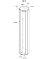
- FIG. 21 is a diagram showing the plane orientation of each crystal plane of the quantum dot 600 shown in FIG. 23A and 23B are cross-sectional views showing plane orientations of crystal planes of the quantum dot 600 shown in FIG.
- the quantum dot 600 according to Embodiment 6 is not limited to the above.
- Quantum dots 600 are, for example, rectangular (11-20) planes, (-2110) planes, (1-210) planes, (-1-120) planes, (2-1-10) planes shown in FIGS. It may be in the shape of an elongated rod including six sides of a plane and a (-12-10) plane.
- the planes equivalent to the (11-20) plane are the (-2110) plane, (1-210) plane, (-1-120) plane, (2-1-10) plane, and (-12-10) plane.
- the quantum dot 600 has a surface between one side and a surface between the other side including, for example, a (0001) equivalent plane and/or a (11-21) equivalent plane. good.
- FIG. 21 is a diagram showing the (11-20) equivalent plane in the crystal plane of the quantum dot 600 shown in FIG.
- the (11-20) equivalent plane is a nonpolar plane.
- the quantum dot 600 may be in the shape of a long rod including 12 sides of the (1-100) equivalent plane and the (11-20) equivalent plane.
- the rod shape includes a dodecagonal prism shape and a shape obtained by truncating one or more corners of a dodecagonal prism.
- FIG. 23 is a cross-sectional view of quantum dot 600 shown in FIG.
- the quantum dot 600 may include, for example, (0001) equivalent planes between the plane between one side of the sides and the plane between the other side of the sides, and/or (1-101 ) equivalent surface and (11-21) equivalent surface.
- the sixth embodiment can also be applied to solar cells as in the first embodiment.
- the quantum dot according to aspect 1 of the present invention has a structure in which 70% or more of the surface area is a polar plane, or 70% or more of the surface area is a non-polar plane.
- the "area ratio" in aspect 1 above is an actual value. As described above, if the ratio of the polar plane (or the non-polar plane) is 60% or more in the analysis result, the area ratio of the polar plane (or the non-polar plane) is 70% or more in the entire light-emitting layer. of quantum dots are considered to be included. Therefore, when the area ratio of the polar plane (or non-polar plane) in the analysis result is 60% or more, at least a part of the quantum dots contained in the quantum dot layer has a sufficient surface with only the polar ligand (or neutral ligand). considered protected.
- the surface may include only polar faces or only non-polar faces.
- the quantum dot layer actually has an area ratio of 100% of the surface of the quantum dot. It is believed to contain quantum dots that are planes (or said non-polar planes).
- the quantum dot according to aspect 3 of the present invention may have a core-shell structure in aspect 1 or 2, and the bandgap of the core may be smaller than the bandgap of the shell.
- the quantum dot according to aspect 4 of the present invention in any one aspect of aspects 1 to 3, has a zinc blende crystal system, and the surface is a (100) plane, a ( ⁇ 100) plane, ( 010) plane, (0-10) plane, (001) plane, and (00-1) plane, (111) plane, (-111) plane, (1-11) plane, (-1-11) plane , (11-1) plane, (-11-1) plane, (1-1-1) plane, and (-1-1-1) plane.
- the quantum dot according to aspect 5 of the present invention in any one aspect of aspects 1 to 3, has a zinc blende crystal system, and the surface is a (100) plane, a ( ⁇ 100) plane, ( 010) plane, (0-10) plane, (001) plane, and (00-1) plane.
- the quantum dot according to aspect 6 of the present invention in any one aspect of aspects 1 to 3, has a zincblende crystal system, and the surfaces are (111) plane, ( ⁇ 111) plane, ( 1-11) plane, (-1-11) plane, (11-1) plane, (-11-1) plane, (1-1-1) plane, and (-1-1-1) plane, It may be a configuration including eight surfaces of.
- the quantum dot according to aspect 7 of the present invention in any one aspect of aspects 1 to 3, has a sodium chloride type crystal system, and the surfaces are (111) plane, ( ⁇ 111) plane, (1 -11) plane, (-1-11) plane, (11-1) plane, (-11-1) plane, (1-1-1) plane, and (-1-1-1) plane, A configuration including eight surfaces may be used.
- the quantum dot according to aspect 8 of the present invention in any one aspect of aspects 1 to 3, has a wurtzite crystal system, and the surface is two of the (0001) plane and the (000-1) plane It may be a configuration including a plane.
- the quantum dot layer according to aspect 9 of the present invention has a configuration including the quantum dots according to any one aspect of aspects 4 to 8 and a polar ligand.
- the quantum dot layer according to aspect 10 of the present invention may have a structure in which 90% or more of the substance amount of ligands contained in the quantum dot layer is the polar ligand.
- the "substance amount ratio" in aspect 10 above is the analysis result. As described above, if the ratio of the polar ligands in the analysis results is 90% or more, it is highly probable that 100% of the ligands actually contained in the quantum dots are the polar ligands.
- the polar ligand has at least one of the structures represented by the following structural formulas (1) to (7). may be
- C represents a carbon atom
- O represents an oxygen atom
- O - represents an oxide ion
- S represents a sulfur atom
- S - represents a sulfide ion
- P represents phosphorus
- the polar ligand has the ionic formula Cl ⁇ , Br ⁇ , I ⁇ , SCN ⁇ , CN ⁇ , OH ⁇ , SH ⁇ , SeH ⁇ , TeH ⁇ , Se 2 ⁇ , S 2 ⁇ , Te 2 ⁇ , Sn 2 S 6 4 ⁇ , Sn 2 Se 6 4 ⁇ , In 2 Se 4 2 ⁇ , In 2 Te 4 2 ⁇ , Ga 2 Se 4 2 ⁇
- the structure may include at least one selected from the group consisting of inorganic polar ligands represented by Sb 2 Se 4 2- and Sb 2 Te 4 2- .
- the quantum dot according to aspect 13 of the present invention in any one aspect of aspects 1 to 3, has a zincblende crystal system, and the surface is a (101) plane, a ( ⁇ 101) plane, ( 011) plane, (0-11) plane, (110) plane, (-110) plane, (1-1-) plane, (-1-10) plane, (10-1) plane, (-10-1 ) plane, (01-1) plane, and (0-1-1) plane.
- the quantum dot according to aspect 14 of the present invention in any one aspect of aspects 1 to 3, has a sodium chloride type crystal system, and the surfaces are (100) plane, ( ⁇ 100) plane, (010 ) plane, (0-10) plane, (001) plane, and (00-1) plane.
- the quantum dot according to aspect 15 of the present invention in any one aspect of aspects 1 to 3, has a wurtzite crystal system, and the surface is (1-100) plane, (0-110) plane , (-1010) plane, (-1100) plane, (01-10) plane, and (10-10) plane, (11-20) plane, (-2110) plane, (1-210) plane, ( A configuration including 12 planes of -1-120) plane, (2-1-10) plane and (-12-10) plane may be employed.
- the quantum dot according to aspect 16 of the present invention in any one aspect of aspects 1 to 3, has a wurtzite crystal system, and the surface is (1-100) plane, (0-110) plane , ( ⁇ 1010) plane, ( ⁇ 1100) plane, (01-10) plane, and (10-10) plane.
- the quantum dot according to aspect 17 of the present invention in any one aspect of aspects 1 to 3, has a wurtzite crystal system, and the surface is (11-20) plane, (-2110) plane, A configuration including six planes of (1-210) plane, (-1-120) plane, (2-1-10) plane, and (-12-10) plane may be employed.
- the quantum dot layer according to aspect 18 of the present invention has a configuration including the quantum dots according to any one of aspects 13 to 17 and a neutral ligand.
- the quantum dot layer according to aspect 19 of the present invention may have a configuration in which, in aspect 18, 90% or more of the ligands contained in the quantum dot layer are the neutral ligands.
- the "substance amount ratio" in aspect 19 above is the analysis result. As described above, if the ratio of the neutral ligands in the analysis results is 90% or more, it is highly probable that 100% of the substance amount ratio of the ligands actually contained in the quantum dots is the neutral ligands. .
- the neutral ligand partially includes at least one structure represented by the following structural formulas (8) to (15) may be
- O represents an oxygen atom
- O- represents an oxide ion
- P represents phosphorus
- R 1 , R 2 and R 3 each independently represent a hydrogen atom, an alkyl group, an aryl group, an alkoxyl group, or an unsaturated hydrocarbon group.
- a light-emitting device has a configuration including the quantum dot layer according to any one of aspects 9 to 12 and aspects 18 to 20.
- a solar cell according to Aspect 22 of the present invention has a configuration including the quantum dot layer according to any one of Aspects 9 to 12 and Aspects 18 to 20.
- the present invention is not limited to the above-described embodiments, but can be modified in various ways within the scope of the claims, and can be obtained by appropriately combining technical means disclosed in different embodiments. is also included in the technical scope of the present invention. Furthermore, new technical features can be formed by combining the technical means disclosed in each embodiment.
Landscapes
- Chemical & Material Sciences (AREA)
- Engineering & Computer Science (AREA)
- Organic Chemistry (AREA)
- Materials Engineering (AREA)
- Inorganic Chemistry (AREA)
- Physics & Mathematics (AREA)
- Nanotechnology (AREA)
- General Physics & Mathematics (AREA)
- Condensed Matter Physics & Semiconductors (AREA)
- Crystallography & Structural Chemistry (AREA)
- Optics & Photonics (AREA)
- Manufacturing & Machinery (AREA)
- Composite Materials (AREA)
- Luminescent Compositions (AREA)
Priority Applications (3)
| Application Number | Priority Date | Filing Date | Title |
|---|---|---|---|
| JP2023505040A JP7594654B2 (ja) | 2021-03-12 | 2021-03-12 | 量子ドット、量子ドット層、発光素子、及び太陽電池 |
| US18/281,151 US20240158691A1 (en) | 2021-03-12 | 2021-03-12 | Quantum dot, quantum dot layer, light-emitting element, and solar cell |
| PCT/JP2021/010042 WO2022190353A1 (ja) | 2021-03-12 | 2021-03-12 | 量子ドット、量子ドット層、発光素子、及び太陽電池 |
Applications Claiming Priority (1)
| Application Number | Priority Date | Filing Date | Title |
|---|---|---|---|
| PCT/JP2021/010042 WO2022190353A1 (ja) | 2021-03-12 | 2021-03-12 | 量子ドット、量子ドット層、発光素子、及び太陽電池 |
Publications (1)
| Publication Number | Publication Date |
|---|---|
| WO2022190353A1 true WO2022190353A1 (ja) | 2022-09-15 |
Family
ID=83226553
Family Applications (1)
| Application Number | Title | Priority Date | Filing Date |
|---|---|---|---|
| PCT/JP2021/010042 Ceased WO2022190353A1 (ja) | 2021-03-12 | 2021-03-12 | 量子ドット、量子ドット層、発光素子、及び太陽電池 |
Country Status (3)
| Country | Link |
|---|---|
| US (1) | US20240158691A1 (https=) |
| JP (1) | JP7594654B2 (https=) |
| WO (1) | WO2022190353A1 (https=) |
Cited By (1)
| Publication number | Priority date | Publication date | Assignee | Title |
|---|---|---|---|---|
| WO2025253844A1 (ja) * | 2024-06-03 | 2025-12-11 | 株式会社Pxp | 太陽電池セル、太陽電池モジュール、及び太陽電池セルの製造方法 |
Citations (3)
| Publication number | Priority date | Publication date | Assignee | Title |
|---|---|---|---|---|
| WO2010023921A1 (ja) * | 2008-09-01 | 2010-03-04 | 学校法人上智学院 | 半導体光素子アレイおよびその製造方法 |
| US20120269721A1 (en) * | 2009-10-12 | 2012-10-25 | The Regents Of The University Of California | Targeted nanoclusters and methods of their use |
| US20130095239A1 (en) * | 2009-10-02 | 2013-04-18 | Hewlett-Packard Development Company, L.P. | Polymer-encapsulated nanoparticle systems |
Family Cites Families (1)
| Publication number | Priority date | Publication date | Assignee | Title |
|---|---|---|---|---|
| KR20120029174A (ko) * | 2010-09-16 | 2012-03-26 | 삼성엘이디 주식회사 | 양자점 발광소자 |
-
2021
- 2021-03-12 US US18/281,151 patent/US20240158691A1/en active Pending
- 2021-03-12 JP JP2023505040A patent/JP7594654B2/ja active Active
- 2021-03-12 WO PCT/JP2021/010042 patent/WO2022190353A1/ja not_active Ceased
Patent Citations (3)
| Publication number | Priority date | Publication date | Assignee | Title |
|---|---|---|---|---|
| WO2010023921A1 (ja) * | 2008-09-01 | 2010-03-04 | 学校法人上智学院 | 半導体光素子アレイおよびその製造方法 |
| US20130095239A1 (en) * | 2009-10-02 | 2013-04-18 | Hewlett-Packard Development Company, L.P. | Polymer-encapsulated nanoparticle systems |
| US20120269721A1 (en) * | 2009-10-12 | 2012-10-25 | The Regents Of The University Of California | Targeted nanoclusters and methods of their use |
Cited By (2)
| Publication number | Priority date | Publication date | Assignee | Title |
|---|---|---|---|---|
| WO2025253844A1 (ja) * | 2024-06-03 | 2025-12-11 | 株式会社Pxp | 太陽電池セル、太陽電池モジュール、及び太陽電池セルの製造方法 |
| JP2025182293A (ja) * | 2024-06-03 | 2025-12-15 | 株式会社Pxp | 太陽電池セル、太陽電池モジュール、及び太陽電池セルの製造方法 |
Also Published As
| Publication number | Publication date |
|---|---|
| JPWO2022190353A1 (https=) | 2022-09-15 |
| US20240158691A1 (en) | 2024-05-16 |
| JP7594654B2 (ja) | 2024-12-04 |
Similar Documents
| Publication | Publication Date | Title |
|---|---|---|
| Wang et al. | Efficient and Color-Tunable Quasi-2D CsPbBr x Cl3–x Perovskite Blue Light-Emitting Diodes | |
| Li et al. | Stoichiometry-controlled InP-based quantum dots: synthesis, photoluminescence, and electroluminescence | |
| Li et al. | Highly luminescent and stable CsPbBr3 perovskite quantum dots modified by phosphine ligands | |
| EP1980652B1 (en) | Multilayer nanocrystal structure and method for producing the same | |
| Kim et al. | Efficient blue-light-emitting Cd-free colloidal quantum well and its application in electroluminescent devices | |
| Lu et al. | Doping up the light: a review of A/B-site doping in metal halide perovskite nanocrystals for next-generation LEDs | |
| US9722198B2 (en) | Nanoparticle material and light-emitting device | |
| KR101738551B1 (ko) | 반도체 나노 결정 | |
| CN110172348A (zh) | 半导体纳米晶体颗粒、其制造方法、和包括其的量子点群及发光器件 | |
| KR101641016B1 (ko) | InP계 양자점 및 그 제조방법 | |
| US12371617B2 (en) | Quantum dots, quantum dot-polymer composite, and electronic device including the same | |
| Han et al. | Giant efficiency and color purity enhancement in multicolor inorganic perovskite light-emitting diodes via heating-assisted vacuum deposition | |
| Li et al. | Consecutive interfacial transformation of cesium lead halide nanocubes to ultrathin nanowires with improved stability | |
| CN110246987A (zh) | 量子点、其制造方法、电致发光器件和显示设备 | |
| US11060026B2 (en) | Electronic device including quantum dots | |
| US11981850B2 (en) | Quantum dots, and an electronic device including the same | |
| EP3786258B1 (en) | Quantum dots and device including the same | |
| Lee et al. | InP-quantum-dot-in-ZnS-matrix solids for thermal and air stability | |
| Liu et al. | Wavelength-tunable green light sources based on ZnO: Ga Nanowire/p-InGaN heterojunctions | |
| Chen et al. | Ligand Engineering Achieves Suppression of Temperature Quenching in Pure Green Perovskite Nanocrystals for Efficient and Thermostable Electroluminescence | |
| Park et al. | Controlling the Phase Distribution of Single Bromide Quasi-2-Dimensional Perovskite Crystals via Solvent Engineering for Pure-Blue Light-Emitting Diodes | |
| WO2022190353A1 (ja) | 量子ドット、量子ドット層、発光素子、及び太陽電池 | |
| Wang et al. | Highly Efficient and Stable Light Emission From Two‐Dimensional/Three‐Dimensional ZnS/Perovskite Heterostructures | |
| Kim | Efficiency enhancement of thermal-evaporated perovskite light-emitting diodes through process optimization and additive engineering | |
| US20210246370A1 (en) | Cadmium free quantum dots, and composite and display device including the same |
Legal Events
| Date | Code | Title | Description |
|---|---|---|---|
| 121 | Ep: the epo has been informed by wipo that ep was designated in this application |
Ref document number: 21930205 Country of ref document: EP Kind code of ref document: A1 |
|
| WWE | Wipo information: entry into national phase |
Ref document number: 2023505040 Country of ref document: JP |
|
| WWE | Wipo information: entry into national phase |
Ref document number: 18281151 Country of ref document: US |
|
| NENP | Non-entry into the national phase |
Ref country code: DE |
|
| 122 | Ep: pct application non-entry in european phase |
Ref document number: 21930205 Country of ref document: EP Kind code of ref document: A1 |