〔実施形態1〕
図1は、本発明の実施形態1に係る自発光素子5を模式的に示す断面図である。自発光素子(発光素子)5は、順構造のトップエミッション型素子であり、アノード51、正孔注入層52、正孔輸送層53、発光層54(量子ドット層)、電子輸送層55、カソード56を含む。
[Embodiment 1]
FIG. 1 is a cross-sectional view schematically showing a self-luminous element 5 according to Embodiment 1 of the present invention. The self-luminous element (light-emitting element) 5 is a forward-structured top-emission element, and includes an anode 51, a hole-injection layer 52, a hole-transport layer 53, a light-emitting layer 54 (quantum dot layer), an electron-transport layer 55, and a cathode. 56.
自発光素子5を形成する各層は、コロイド溶液塗布、塗布焼成、メタルマスクを援用するスパッタ、フォトリソグラフィ、樹脂充填、アッシング及びドライ/ウエットエッチング等の成膜及びパターニングにより作製できる。
Each layer forming the self-luminous element 5 can be produced by film formation and patterning such as colloid solution coating, coating baking, sputtering using a metal mask, photolithography, resin filling, ashing and dry/wet etching.
(アノード)
アノード51は、導電性を有する材料を含む電極部材である。自発光素子5が順構造のトップエミッションである場合、取り出し効率の向上の観点から、アノード51は、反射電極であることが好ましい。アノード51が反射電極である場合、例えば、アノード51は、Al、Ag、あるいはこれらの合金からなっていてもよい。ただし、これらに限られず、アノード51は、透明の導電材料からなっていてもよく、この場合、後述する正孔注入層52との準位整合を考慮すれば、ITO(Indium Tin Oxide)を含むことが好ましい。アノード51は、各材料をスパッタ法により成膜することによって作製してもよい。アノード51の層厚は、例えば100nm以下である。他にも、アノード51は、ITOからなる導電層の下層に、ポリイミド等の絶縁層を介してAlまたはAgからなる反射層を設けることにより形成してもよい。その場合、絶縁層と反射層とに、導電層であるITOをTFTと接続させるためのコンタクトホールをフォトリソグラフィにより形成してもよい。
(anode)
The anode 51 is an electrode member containing a conductive material. When the self-luminous element 5 has a forward structure top emission, the anode 51 is preferably a reflective electrode from the viewpoint of improving extraction efficiency. When the anode 51 is a reflective electrode, the anode 51 may be made of Al, Ag, or alloys thereof, for example. However, the anode 51 is not limited to these, and may be made of a transparent conductive material. is preferred. The anode 51 may be produced by depositing each material by a sputtering method. The layer thickness of the anode 51 is, for example, 100 nm or less. Alternatively, the anode 51 may be formed by providing a reflective layer made of Al or Ag below a conductive layer made of ITO via an insulating layer such as polyimide. In that case, a contact hole may be formed in the insulating layer and the reflective layer by photolithography for connecting the ITO, which is a conductive layer, to the TFT.
(正孔注入層)
正孔注入層52は、正孔注入性材料を含み、陽極から後述する正孔輸送層53への正孔注入効率を高める機能を有する層である。正孔注入層52に有機材料を用いる場合、当該有機材料は、アノード51の仕事関数に整合するHOMO準位を有するPEDOTが好ましい。正孔注入層52は、例えば、PEDOTを含む塗材を塗布した後、150℃程度でPEDOTを硬化することにより作製してもよい。
(hole injection layer)
The hole injection layer 52 is a layer that contains a hole injection material and has a function of increasing the efficiency of hole injection from the anode to the hole transport layer 53 described below. When an organic material is used for the hole injection layer 52 , the organic material is preferably PEDOT having a HOMO level matching the work function of the anode 51 . The hole injection layer 52 may be produced, for example, by applying a coating material containing PEDOT and then curing the PEDOT at about 150.degree.
自発光素子5の長期信頼性向上の観点からは、正孔注入層52が、無機物であることが好ましい。正孔注入層52の無機材料としては、p型のNiO、LaO3、LaNiO、ZnO、MgZnO、深いCBMを持ちn型のMoO3、WO3等、一般に正孔注入層52に用いられる無機物、特には金属酸化物等でよい。正孔注入層52の成膜は、スパッタあるいは蒸着により行うことが可能である。しかしながら、正孔注入層52の材料をナノ粒子化することが可能であれば、正孔注入層52は、適切なコロイド溶液を用いて、塗布により形成することもできる。
From the viewpoint of improving the long-term reliability of the self-luminous element 5, the hole injection layer 52 is preferably made of an inorganic substance. Examples of the inorganic material for the hole injection layer 52 include p-type NiO, LaO 3 , LaNiO, ZnO, MgZnO, n-type MoO 3 and WO 3 having deep CBM, and inorganic materials generally used for the hole injection layer 52. In particular, it may be a metal oxide or the like. The hole injection layer 52 can be formed by sputtering or vapor deposition. However, if the material of the hole injection layer 52 can be made into nanoparticles, the hole injection layer 52 can also be formed by coating using a suitable colloidal solution.
なお、正孔注入層52は必須ではなく、所望の素子構造及び特性に合わせて省略してもよい。
Note that the hole injection layer 52 is not essential, and may be omitted depending on the desired device structure and characteristics.
(正孔輸送層)
正孔輸送層53は、正孔輸送性材料を含み、発光層54への正孔輸送効率を高める機能を有する層である。正孔輸送層53に有機材料を用いる場合、当該有機材料には、PVK、TFB、Poly-TPD等を含む、HOMO準位が発光層材料に整合する有機材料を採用することが好ましい。また、正孔輸送層53には、NiO、MgNiO、MgNiO、LaNiO等、VBMが発光層材料に整合する金属残化物、または、p型ZnO等の半導体材料を用いてもよい。例えば、正孔輸送層53の材料にPVKを用いる場合、PVKをトルエン等の溶媒に溶かした溶液を塗布することにより形成してもよい。また、正孔輸送層53の材料に無機材料を用いる場合、スパッタあるいは蒸着を用いて成膜すればよい。正孔輸送層53が、ナノ粒子化が可能な材料を含む場合には、正孔輸送層53を塗布により形成してもよい。
(Hole transport layer)
The hole-transporting layer 53 is a layer containing a hole-transporting material and having a function of increasing the efficiency of transporting holes to the light-emitting layer 54 . When an organic material is used for the hole transport layer 53, it is preferable to adopt an organic material whose HOMO level matches that of the light-emitting layer material, such as PVK, TFB, and Poly-TPD. Further, the hole transport layer 53 may be made of a metal residue such as NiO, MgNiO, MgNiO, LaNiO, etc. whose VBM matches the light-emitting layer material, or a semiconductor material such as p-type ZnO. For example, when PVK is used as the material of the hole transport layer 53, the hole transport layer 53 may be formed by applying a solution of PVK dissolved in a solvent such as toluene. When an inorganic material is used as the material for the hole transport layer 53, the film may be formed using sputtering or vapor deposition. When the hole transport layer 53 contains a material that can be made into nanoparticles, the hole transport layer 53 may be formed by coating.
(発光層)
発光層54は、量子ドット100を含む。量子ドット100の構造の詳細については、参照する図面を代えて後述する。発光層54はさらに、極性リガンド2を含む。極性リガンド2についても、参照する図面を代えて後述する。本明細書において「リガンド」は、量子ドットの表面に現に結合しているリガンドだけでなく、表面に結合可能なものの結合していないリガンドも包含する。
(Light emitting layer)
Emissive layer 54 includes quantum dots 100 . Details of the structure of the quantum dot 100 will be described later with reference to drawings replaced. Emissive layer 54 further comprises polar ligands 2 . The polar ligand 2 will also be described later with reference to different drawings. As used herein, "ligand" includes not only ligands that are actually bound to the surface of the quantum dots, but also ligands that are capable of binding to the surface but are not bound.
(電子輸送層)
電子輸送層55は、電子輸送材料を含み、発光層54への電子輸送効率を高める機能を有する層である。電子輸送層55の材料としては、ZnO、IZO、ZAO、ZnMgO等のZnO系無機材料、あるいは、TiO2を用いることができる。ただし、電子輸送層55は、これに限られず、有機材料を含んでいてもよい。電子輸送層55の成膜は例えばスパッタまたはコロイド溶液の塗布により行われる。
(Electron transport layer)
The electron-transporting layer 55 is a layer containing an electron-transporting material and having a function of increasing electron transport efficiency to the light-emitting layer 54 . As a material of the electron transport layer 55, a ZnO-based inorganic material such as ZnO, IZO, ZAO, ZnMgO, or TiO 2 can be used. However, the electron transport layer 55 is not limited to this and may contain an organic material. The electron transport layer 55 is formed by, for example, sputtering or applying a colloidal solution.
(カソード)
カソード56は、導電性を有する材料を含む電極部材である。カソード56は、電子輸送層55と同じく、従来から用いられているAlまたはAg等の比較的浅い仕事関数を持つ金属を蒸着またはスパッタを用いて成膜する。
(cathode)
Cathode 56 is an electrode member containing a conductive material. As with the electron transport layer 55, the cathode 56 is formed by depositing or sputtering a conventionally used metal such as Al or Ag, which has a relatively shallow work function.
本実施形態に係る自発光素子5はトップエミッション型素子であるが、自発光素子の構造はこれに限られず、ボトムエミッション型であってもよい。自発光素子5がボトムエミッション型素子である場合、アノード51は透過電極であり、カソード56は反射電極であってもよい。自発光素子5は、順構造であっても逆構造であってもよい。例えば、自発光素子5が逆構造である場合、自発光素子5は、各層が、図1に記載した積層順と逆順に積層された構造を有していてもよい。
Although the self-luminous element 5 according to this embodiment is a top emission type element, the structure of the self-luminous element is not limited to this, and may be a bottom emission type. When the self-luminous element 5 is a bottom emission type element, the anode 51 may be a transmissive electrode and the cathode 56 may be a reflective electrode. The self-luminous element 5 may have a forward structure or a reverse structure. For example, when the self-luminous element 5 has an inverted structure, the self-luminous element 5 may have a structure in which each layer is laminated in the reverse order of the lamination order shown in FIG.
上述の各層は、より優れた特性を持つ材料が見いだされれば適宜置き換えて素子を構成することができる。
Each of the layers described above can be replaced as appropriate to form an element if a material with better properties is found.
(ミラーの面指数および方向指数)
本明細書において、結晶面を特定するためにミラーの面指数を用いる。すなわち、六方晶系以外の結晶に関して、単位格子ベクトルa1、a2、a3および整数h、k、lを用いて、1/h*ベクトルa1、1/k*ベクトルa2、1/l×ベクトルa3で指定される3点を通る結晶面を、(hkl)面と称する。また、六方晶系の結晶に関して、a4:=-a1-a2で定義される単位格子ベクトルa4およびl:=-h-kで定義される整数mをさらに用いて、上記3点を通る結晶面を、(hkml)面と称する。
(mirror plane index and orientation index)
Herein, the mirror plane index is used to specify the crystal planes. That is, for non-hexagonal crystals, using unit cell vectors a 1 , a 2 , a 3 and integers h, k, l, 1/h* vector a 1 , 1/k* vector a 2 , 1/ A crystal plane passing through the three points specified by the l×vector a3 is called the (hkl) plane. Further, with respect to the hexagonal crystal, further using the unit cell vector a 4 defined by a 4 :=-a 1 -a 2 and the integer m defined by l :=-hk, the above three points A crystal plane passing through is called a (hkml) plane.
本明細書において、六方晶系以外の結晶に関して、(hkl)面および(hkl)面と等価な面を包括して、(hkl)等価面と称する。また、六方晶系の結晶に関して、(hkml)面および(hkml)面と等価な面を包括して、(hkml)等価面と称する。
In this specification, regarding crystals other than the hexagonal system, the (hkl) plane and the plane equivalent to the (hkl) plane are collectively referred to as the (hkl) equivalent plane. In addition, with respect to hexagonal crystals, the (hkml) plane and the plane equivalent to the (hkml) plane are collectively referred to as the (hkml) equivalent plane.
本明細書において、結晶方向を特定するためにミラーの方向指数を用いる。すなわち、六方晶系以外の結晶に関して、単位格子ベクトルa1、a2、a3および整数p、q、rを用いて、p*ベクトルa1+q*ベクトルa2+r×ベクトルa3で指定される合成ベクトルに沿った方向を、[pqr]方向と称する。また、六方晶系の結晶に関して、a4:=-a1-a2で定義される単位格子ベクトルa4およびs:=-p-qで定義される整数sをさらに用いて、上記合成ベクトルに沿った方向を、[pqsr]方向と称する。
The orientation index of the mirror is used herein to specify the crystal orientation. That is, for crystals other than the hexagonal system, using unit cell vectors a 1 , a 2 , a 3 and integers p, q, r, p*vector a 1 +q*vector a 2 +r×vector a 3 The direction along the composite vector that Further, for a hexagonal crystal, further using the unit cell vector a 4 defined by a 4 :=-a 1 -a 2 and the integer s defined by s:=-pq, the above composite vector is called the [pqsr] direction.
(量子ドットの構造)
図2は本実施形態1に係る量子ドット100の一例の構造を示す斜視図である。図3及び図4は、図2に示した量子ドット100の各結晶面の面方位を示す図である。図5は、図2に示した量子ドット100の表面と、当該表面を保護する極性リガンドとを概略的に示す模式図である。
(Structure of quantum dots)
FIG. 2 is a perspective view showing an example structure of the quantum dot 100 according to the first embodiment. 3 and 4 are diagrams showing the plane orientation of each crystal plane of the quantum dot 100 shown in FIG. FIG. 5 is a schematic diagram schematically showing the surface of the quantum dot 100 shown in FIG. 2 and the polar ligands protecting the surface.
本実施形態1に係る量子ドット100は、閃亜鉛鉱型の結晶系を有する。量子ドット100は、閃亜鉛鉱型の結晶系を自発的に取り得る材料を含む群から選択される少なくとも1つを含むことが好ましい。当該材料は例えば、ZnS,CdSe,ZnSeなどのII―VI族化合物および、InPなどのIII-V族化合物である。本開示において、II-VI族化合物とはII族元素とVI族元素を含む化合物を意味し、III-V族化合物はIII族元素とV族元素を含む化合物を意味する。また、II族元素とは2族元素および12族元素を含み、III族元素とは3族元素および13族元素を含み、V族元素は5族元素および15族元素を含み、VI族元素は6族元素および16族元素を含み得る。また、ローマ数字を用いた元素の族は旧CAS方式に基づき、アラビア数字を用いた元素の族は、IUPACの現行命名法に基づく。
The quantum dot 100 according to Embodiment 1 has a zinc blende crystal system. Quantum dot 100 preferably includes at least one selected from the group including materials capable of spontaneously adopting a zinc-blende crystal system. Such materials are, for example, II-VI compounds such as ZnS, CdSe, ZnSe and III-V compounds such as InP. In this disclosure, a group II-VI compound means a compound containing a group II element and a group VI element, and a group III-V compound means a compound containing a group III element and a group V element. Group II elements include Group 2 elements and Group 12 elements, Group III elements include Group 3 elements and Group 13 elements, Group V elements include Group 5 elements and Group 15 elements, and Group VI elements include Group 6 and 16 elements may be included. Also, the groups of elements with Roman numerals are based on the old CAS system, and the groups of elements with Arabic numerals are based on the current IUPAC nomenclature.
量子ドット100は、コア構造、コアシェル構造または、コアマルチシェル構造の何れであってもよい。本明細書において「量子ドット100の表面」は、量子ドット100の最外層の表面を意味する。本明細書において「量子ドット100の結晶面」は、量子ドット100の最外層の結晶面を意味する。本明細書において「量子ドット100の結晶系」は、量子ドット100の最外層の結晶系を意味する。
The quantum dot 100 may have a core structure, a core-shell structure, or a core-multi-shell structure. In this specification, the “surface of the quantum dots 100” means the surface of the outermost layer of the quantum dots 100. In this specification, the “crystal plane of the quantum dot 100” means the crystal plane of the outermost layer of the quantum dot 100. In this specification, “the crystal system of the quantum dots 100 ” means the crystal system of the outermost layer of the quantum dots 100 .
量子ドット100がコアシェル構造である場合、コアの結晶系とシェルの結晶系とは、互いに同じでも異なってもよい。量子ドット100がコアマルチシェル構造である場合も同様に、コアの結晶系とマルチシェルの最内層の結晶系とは互いに同じでも異なってもよく、マルチシェルの互いに隣接する層の結晶系は互いに同じでも異なってもよい。複数の層を積層する場合、ある層が薄ければ(典型的には、3原子層以下であれば)、当該層の結晶系は通常、当該層の下層の結晶系に従うことが知られている。一方、ある層が厚ければ、当該層の結晶系は通常、当該層を形成する材料がバルクで自発的に取り得る結晶系の1つに従うことが知られている。
When the quantum dot 100 has a core-shell structure, the crystal system of the core and the crystal system of the shell may be the same or different. Similarly, when the quantum dot 100 has a core multishell structure, the crystal system of the core and the crystal system of the innermost layer of the multishell may be the same or different, and the crystal systems of the adjacent layers of the multishell may be different from each other. They can be the same or different. It is known that when a plurality of layers are stacked, if a layer is thin (typically, three atomic layers or less), the crystal system of the layer usually conforms to the crystal system of the lower layer of the layer. there is On the other hand, it is known that if a layer is thick, the crystal system of that layer usually follows one of the crystal systems that the material forming the layer can spontaneously adopt in bulk.
量子ドット100がコアシェル構造を有する場合、正孔と電子とをコアで捕捉して再結合させるために、コアのバンドギャップはシェルのバンドギャップよりも小さいことが好ましい。具体的には、コアの電子親和力がシェルの電子親和力よりも大きく、かつ、コアのイオン化エネルギーがシェルのイオン化エネルギーよりも小さいことが好ましい。
When the quantum dot 100 has a core-shell structure, the bandgap of the core is preferably smaller than the bandgap of the shell in order to trap and recombine holes and electrons in the core. Specifically, it is preferable that the electron affinity of the core is higher than the electron affinity of the shell and the ionization energy of the core is lower than the ionization energy of the shell.
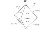
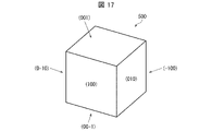
量子ドット100は、複数の結晶面を有する多面体の結晶であり、その表面が主に極性面である。量子ドット100の表面は例えば、(a)図4に示す四角形の(100)面、(-100)面、(010)面、(0-10)面、(001)面、及び(00-1)面と、(b)図3に示す六角形の(111)面、(-111)面、(1-11)面、(-1-11)面、(11-1)面、(-11-1)面、(1-1-1)面、及び(-1-1-1)面と、の14面を含む。この場合、量子ドット100の理想的な形状は、正八面体の各頂点を正方形で切り取って得られる十四面体である。
The quantum dot 100 is a polyhedral crystal having a plurality of crystal planes, the surfaces of which are mainly polar planes. The surface of the quantum dot 100 is, for example, (a) the quadrangular (100) plane, (-100) plane, (010) plane, (0-10) plane, (001) plane, and (00-1) plane shown in FIG. ) plane, and (b) the hexagonal (111) plane, (-111) plane, (1-11) plane, (-1-11) plane, (11-1) plane, (-11 -1), (1-1-1), and (-1-1-1) 14 planes. In this case, the ideal shape of the quantum dot 100 is a tetradecahedron obtained by cutting each vertex of a regular octahedron into squares.
図3は、量子ドット100の結晶面において(111)面と等価な面を示す図である。図3において、(111)面および(111)面と等価な面には、ハッチング処理を施している。量子ドット100の結晶面のうち、(111)面と等価な面は、(-111)面、(1-11)面、(-1-11)面、(11-1)面、(-11-1)面、(1-1-1)面、及び(-1-1-1)面である。図4は、量子ドット100の結晶面において(100)面と等価な面を示す図である。図4において、(100)面および(100)面と等価な面には、ハッチング処理を施している。量子ドット100の結晶面のうち、(100)面と等価な面は、(-100)面、(010)面、(0-10)面、(001)面、及び(00-1)面である。
FIG. 3 is a diagram showing a plane equivalent to the (111) plane among the crystal planes of the quantum dot 100. FIG. In FIG. 3, the (111) plane and planes equivalent to the (111) plane are hatched. Among the crystal planes of the quantum dot 100, planes equivalent to the (111) plane are the (-111) plane, (1-11) plane, (-1-11) plane, (11-1) plane, (-11 -1) plane, (1-1-1) plane, and (-1-1-1) plane. FIG. 4 is a diagram showing a plane equivalent to the (100) plane among the crystal planes of the quantum dot 100. As shown in FIG. In FIG. 4, the (100) plane and planes equivalent to the (100) plane are hatched. Among the crystal planes of the quantum dot 100, the planes equivalent to the (100) plane are the (-100) plane, (010) plane, (0-10) plane, (001) plane, and (00-1) plane. be.
閃亜鉛鉱型の結晶系における(111)等価面および(100)等価面は、極性面である。極性面とは、表面に露出している陽イオンの価数と陰イオンの価数とが偏っている結晶面である。具体的には、極性面とは、表面に陽イオンが陰イオンよりも多く存在することで正に帯電している面で、負に帯電する極性リガンドと強く結合することができる面である。対照的に、非極性面とは、露出している陽イオンの価数と陰イオンの価数とが釣り合っている結晶面である。具体的には、非極性面とは、表面が電気的に中性で帯電は無く、非極性リガンドと強く結合することができる面である。
The (111) equivalent plane and the (100) equivalent plane in the sphalerite-type crystal system are polar planes. A polar plane is a crystal plane in which the valences of cations and anions exposed on the surface are biased. Specifically, the polar surface is a surface that is positively charged due to the presence of more cations than anions on the surface, and that can strongly bind to a negatively charged polar ligand. In contrast, non-polar planes are crystal planes in which the valences of exposed cations and anions are in balance. Specifically, a non-polar surface is a surface that is electrically neutral, has no charge, and can strongly bind to a non-polar ligand.
なお、極性面であるか、非極性面であるかの特定方法は、下記「(量子ドットの結晶面分析方法)」に記載する方法で特定することができる。量子ドット100の表面が極性面である場合、図5に示すように、極性リガンド2を用いて量子ドット100の表面を保護(表面保護)できる。極性リガンド2は、極性面に非共有電子対を介して配位結合できる。
The method for identifying whether it is a polar face or a non-polar face can be specified by the method described in "(Quantum dot crystal face analysis method)" below. When the surface of the quantum dot 100 is a polar plane, the surface of the quantum dot 100 can be protected (surface protection) using the polar ligand 2, as shown in FIG. A polar ligand 2 can coordinate to a polar face via a lone pair of electrons.
量子ドットの極性面の割合と発光素子の耐久時間との関係性について、表面の面積比50%が極性面であり、極性リガンドのみを配位させた量子ドットを用い、量子ドット発光素子を作製し耐久時間を測定した。その結果、駆動輝度1000cd/m2にて輝度半減時間が約6400時間という結果が得られた。さて、極性面が50%ということは、残り50%の面は非極性面である。これらの非極性面では極性リガンドとの間の結合が弱く、これらの非極性面からは極性リガンドが脱離しやすい。リガンドの脱離は、量子ドット表面での欠陥準位を発生させ、この欠陥準位を経由して励起子の非発光再結合が引き起こされる。したがってこの場合、表面に欠陥準位が存在する割合で非発光再結合確率が決まると仮定すると、非発光再結合確率を0.5paと表せる(非極性面が50%であるため)。ここで、paは、表面の面積比100%が非極性面であり、極性リガンドのみを配位させた量子ドットを用いた場合に、非極性面から極性リガンドが外れて欠陥準位が形成され、この欠陥準位を経由して励起子の非発光再結合が引き起こされる確率をpa(0<pa<1)としている。
Regarding the relationship between the ratio of the polar plane of the quantum dot and the durability time of the light-emitting device, a quantum dot light-emitting device was manufactured using a quantum dot in which 50% of the surface area was a polar plane and only polar ligands were coordinated. and measured the endurance time. As a result, it was found that the luminance half life time was about 6400 hours at a driving luminance of 1000 cd/m 2 . Now, 50% of the polar faces means that the remaining 50% of the faces are non-polar faces. These non-polar faces are weakly bound to polar ligands, and polar ligands tend to detach from these non-polar faces. Detachment of the ligand generates defect levels on the quantum dot surface through which non-radiative recombination of excitons is triggered. Therefore, in this case, assuming that the non-radiative recombination probability is determined by the ratio of defect levels existing on the surface, the non-radiative recombination probability can be expressed as 0.5pa (because the nonpolar plane is 50%). Here, 100% of the surface area of p a is a non-polar plane, and when quantum dots with only polar ligands coordinated are used, the polar ligands deviate from the non-polar planes to form defect levels. and the probability of causing non-radiative recombination of excitons via this defect level is pa (0<p a < 1).
なお非発光再結合は量子ドットに熱エネルギーを与え、ある確率で量子ドットを失活させる。非発光再結合によりQDが失活する確率をpb(0<pb<1)とすると、一回の励起子再結合にかかる平均時間当たりにQDが失活する確率は0.5papbであると考えられる。
The non-radiative recombination gives thermal energy to the quantum dots and deactivates the quantum dots with a certain probability. If the probability of QD deactivation due to non-radiative recombination is p b (0 < p b < 1), the probability of QD deactivation per average time taken for one exciton recombination is 0.5 p a p b .
上記で0.5としていた非極性面の割合を一般化してc、時間tでの失活していない量子ドットの数をN(t)、また単位時間における励起子再結合の平均回数をfとすると、単位時間当たりに失活する量子ドットの量dN/dtは、
dN/dt=-papbcfN(t)
となる。失活していない量子ドットの数N(t)と量子ドット発光素子の輝度L(t)とは比例関係であるためN=kLとすると(kは任意の正の実数)、
dL/dt=-papbcfkL(t) (1)
と表すことができる。(1)式の解は初期条件L(0)=L0とすると、
L(t)=L0・exp(-papbcfkt) (2)
となる。
Generalizing the ratio of nonpolar planes, which was set to 0.5 above, c, the number of undeactivated quantum dots at time t is N(t), and the average number of exciton recombination per unit time is f Then, the amount dN/dt of quantum dots deactivated per unit time is
dN/dt=-p a p b cfN(t)
becomes. Since there is a proportional relationship between the number N(t) of quantum dots that have not been deactivated and the luminance L(t) of the quantum dot light-emitting element, if N=kL (k is any positive real number),
dL/dt=-p a p b cfkL(t) (1)
It can be expressed as. Assuming the initial condition L( 0 )=L0 for the solution of equation (1),
L(t)=L 0 ·exp(−p a p b cfkt) (2)
becomes.
(2)式より輝度半減時間t1/2は、
t1/2=In(2)/papbcfk (3)
となる。(3)式に実験値であるc=0.5、t1/2=6400時間を代入するとpapbfk≒2.17×10^-4となり、(3)式は、
t1/2=3200/λ (4)
となる。ここで極性面の割合がそれぞれ70%、80%、90%である場合、非極性面の割合cがそれぞれ0.3、0.2、0.1となり、これらを(4)に代入すると、輝度半減時間t1/2はそれぞれ、10667時間、16000時間、32000時間となる。本願の量子ドットを含む発光素子をテレビのディスプレイに使用することを想定し、一日当たりのテレビ視聴時間を3時間とするとこれらの値は9.74年、14.6年、29.2年という年数となる。
From the equation (2), the luminance half-life time t 1/2 is
t 1/2 =In(2)/p a p b cfk (3)
becomes. Substituting the experimental values of c = 0.5 and t 1/2 = 6400 hours into the equation (3) yields p a p b fk ≈ 2.17 × 10^-4, and the equation (3) is:
t 1/2 =3200/λ (4)
becomes. Here, when the proportions of polar planes are 70%, 80%, and 90%, respectively, the proportions c of non-polar planes are 0.3, 0.2, and 0.1, respectively. The luminance half life time t 1/2 is 10667 hours, 16000 hours and 32000 hours, respectively. Assuming that the light-emitting device containing the quantum dots of the present application is used for a television display, and the television viewing time per day is 3 hours, these values are 9.74 years, 14.6 years, and 29.2 years. number of years.
以上より、量子ドット発光層54が、量子ドット100を表面保護するリガンドとして、極性リガンド2のみを含む構成について、自発光素子の耐久時間を想定した。量子ドット100の表面に極性面が占める割合(以降、「極性面の面積比」と称する)が70%である量子ドット100を用いた自発光素子5について、1000cd/m2での輝度半減時間1万時間以上の結果が見込まれる。1000cd/m2での輝度半減時間1万時間以上は、ディスプレイの耐用年数に換算して約10年に相当する。耐用年数10年は、一般に、商業的な製品化において、十分な耐久寿命である。また、極性面の面積比が80%以上である量子ドット100を用いた青色発光の自発光素子5について、ディスプレイの耐用年数に換算して約15年に相当する結果が見込まれる。また、極性面の面積比が90%以上である量子ドット100を用いた青色発光の自発光素子5について、ディスプレイの耐用年数に換算して約30年に相当する結果が見込まれる。
Based on the above, the endurance time of the self-luminous element was assumed for the configuration in which the quantum dot light-emitting layer 54 contains only the polar ligand 2 as the ligand that protects the surface of the quantum dot 100 . Luminance half-life time at 1000 cd/m 2 for the self-luminous element 5 using the quantum dots 100 in which the ratio of the polar planes to the surface of the quantum dots 100 (hereinafter referred to as the “area ratio of the polar planes”) is 70% More than 10,000 hours of results are expected. A brightness half life of 10,000 hours or more at 1000 cd/m 2 corresponds to about 10 years of service life of the display. A service life of 10 years is generally sufficient for commercial production. In addition, the self-luminous element 5 that emits blue light using the quantum dots 100 having a polar surface area ratio of 80% or more is expected to have a useful life equivalent to about 15 years of the display. In addition, the self-luminous element 5 that emits blue light using the quantum dots 100 having a polar surface area ratio of 90% or more is expected to have a useful life equivalent to about 30 years of the display.
したがって、量子ドット100の表面の70%以上が極性面である場合、極性リガンド2のみを用いて量子ドット100の表面を十分に保護(表面保護)できる。
Therefore, when 70% or more of the surface of the quantum dot 100 is a polar plane, the surface of the quantum dot 100 can be sufficiently protected (surface protected) using only the polar ligand 2.
量子ドット100の表面における極性面の面積比が高いほど、極性リガンド2による表面保護の効果が向上する。故に、本実施形態1に係る量子ドット100の表面は、面積比70%以上が極性面であればよく、80%以上が極性面であることが好ましく、90%以上が極性面であることがより好ましい。また、量子ドット100の表面が極性面のみを含むことが理想的である。
The higher the area ratio of the polar planes on the surface of the quantum dot 100, the more effectively the polar ligand 2 protects the surface. Therefore, the surface of the quantum dot 100 according to Embodiment 1 may be a polar surface with an area ratio of 70% or more, preferably 80% or more is a polar surface, and 90% or more is a polar surface. more preferred. Also, ideally, the surface of the quantum dot 100 contains only polar planes.
ここで、量子ドットの表面のうち、極性面と非極性面とにおける、極性リガンドの結合エネルギーを評価することにより、極性リガンドまたは中性リガンドによる、量子ドットの表面の保護効果を評価する。具体的には、量子ドット100の表面がCdSeから成り、極性リガンド2がカルボン酸系リガンドである場合について、量子ドット100の表面に対する極性リガンド2の1molあたりの結合エネルギーを計算した。当該計算は、密度汎関数法(Density Functional Theory:DFT)に基づいて計算した。この計算結果において、極性面である(100)等価面及び(111)等価面に対する結合エネルギーが240kcal/mol程度である一方、非極性面である(110)等価面に対する結合エネルギーが16kcal/mol程度である。
Here, the protective effect of the quantum dot surface by the polar ligand or the neutral ligand is evaluated by evaluating the binding energy of the polar ligand on the polar plane and the non-polar plane of the quantum dot surface. Specifically, when the surface of the quantum dot 100 is made of CdSe and the polar ligand 2 is a carboxylic acid-based ligand, the binding energy per 1 mol of the polar ligand 2 to the surface of the quantum dot 100 was calculated. The calculation was based on the density functional theory (DFT). According to the calculation results, the binding energy for the (100) equivalent plane and the (111) equivalent plane, which are polar planes, is about 240 kcal/mol, while the binding energy for the (110) equivalent plane, which is a nonpolar plane, is about 16 kcal/mol. is.
このように、結合エネルギーが1桁以上異なるので、極性面の割合が制御されていない従来の量子ドットを極性リガンド2のみで表面保護した場合、非極性面から従来の量子ドットの劣化が進行する。また、従来の量子ドットを後述の中性リガンド3のみで表面保護した場合、極性面から従来の量子ドットの劣化が進行する。このため、特許文献1,2のような従来技術では、極性リガンドと中性リガンドの両方を用いて従来の量子ドットを表面保護するために、極性リガンドと中性リガンドとを混合する工程またはリガンド交換する工程を必要とする。
In this way, since the binding energy differs by more than one order of magnitude, when conventional quantum dots in which the ratio of polar planes is not controlled are surface-protected only with polar ligand 2, the conventional quantum dots deteriorate from the non-polar planes. . Further, when conventional quantum dots are surface-protected only with a neutral ligand 3 described later, the deterioration of conventional quantum dots progresses from the polar side. For this reason, in conventional techniques such as Patent Documents 1 and 2, in order to protect the surface of conventional quantum dots using both polar ligands and neutral ligands, a process of mixing polar ligands and neutral ligands or ligands A replacement process is required.
これに対して、本実施形態1に係る量子ドット100では、極性面の面積比が70%以上である。したがって、量子ドット100における非極性面の面積比が小さい。また、量子ドット100の極性面に結合している極性リガンド2が当該量子ドット100の非極性面への他の量子ドット100の接近を阻害する。これらの結果、量子ドット100を極性リガンド2のみで表面保護しても、量子ドット100の非極性面は劣化しにくい。このため、本実施形態1に係る発光層54の製造方法は、極性リガンドと中性リガンドとを混合する工程もリガンド交換する工程も必要としない。したがって、本実施形態1に係る発光層54は、製造効率が高い。また、量子ドット100の表面保護のために用いるリガンドを、単一種とし得る。
On the other hand, in the quantum dot 100 according to Embodiment 1, the area ratio of the polar plane is 70% or more. Therefore, the area ratio of the nonpolar plane in the quantum dot 100 is small. In addition, the polar ligand 2 bound to the polar face of the quantum dot 100 blocks access of other quantum dots 100 to the non-polar face of the quantum dot 100 . As a result, even if the quantum dot 100 is surface-protected only with the polar ligand 2, the non-polar surface of the quantum dot 100 is less likely to deteriorate. Therefore, the method for manufacturing the light-emitting layer 54 according to Embodiment 1 does not require a process of mixing a polar ligand and a neutral ligand or a process of exchanging ligands. Therefore, the light-emitting layer 54 according to Embodiment 1 has high manufacturing efficiency. Moreover, the ligand used for the surface protection of the quantum dot 100 can be made into a single species.
極性リガンド2は、有機であってもよく、例えば、末端にチオール基、アルコキシル基、カルボキシル基、ホスホン酸基、及びホスフィン酸基の何れか1つ以上を含む有機極性リガンドから成る群から選択される少なくとも1種を含む。末端に一つ以上のチオール基を含むリガンドは、電離した状態で、下記構造式(1)または下記構造式(2)で表される構造を一部に含む。末端にアルコキシル基を含むリガンドは、電離した状態で、下記構造式(3)で表される構造を一部に含む。末端にカルボキシル基を含むリガンドは、電離した状態で、下記構造式(4)で表される構造を一部に含む。末端にホスホン酸基を含むリガンドは、電離した状態で、下記構造式(5)または下記構造式(6)で表される構造を一部に含む。末端にホスフィン酸基を含むリガンドは、電離した状態で、下記構造式(7)で表される構造を一部に含む。
The polar ligand 2 may be organic, for example, selected from the group consisting of organic polar ligands containing one or more of a terminal thiol group, an alkoxyl group, a carboxyl group, a phosphonic acid group, and a phosphinic acid group. contains at least one A ligand containing one or more thiol groups at its terminal partly contains a structure represented by the following structural formula (1) or the following structural formula (2) in an ionized state. A ligand containing an alkoxyl group at its terminal partly contains a structure represented by the following structural formula (3) in an ionized state. A ligand containing a terminal carboxyl group partially contains a structure represented by the following structural formula (4) in an ionized state. A ligand containing a phosphonic acid group at its terminal partly contains a structure represented by the following structural formula (5) or the following structural formula (6) in an ionized state. A ligand containing a phosphinic acid group at its terminal partly contains a structure represented by the following structural formula (7) in an ionized state.
なお、上記構造式(1)~(7)において、Cは炭素原子を示し、Oは酸素原子を示し、O-は酸化物イオンを示し、Sは硫黄原子を示し、S-は硫化物イオンを示し、Pはリン原子を示し、R1およびR2は、それぞれ独立して、水素原子、アルキル基、アリール基、アルコキシル基、または不飽和炭化水素基を示す。
In the structural formulas (1) to (7) above, C represents a carbon atom, O represents an oxygen atom, O - represents an oxide ion, S represents a sulfur atom, and S - represents a sulfide ion. , P represents a phosphorus atom, and R 1 and R 2 each independently represent a hydrogen atom, an alkyl group, an aryl group, an alkoxyl group, or an unsaturated hydrocarbon group.
極性リガンド2は、有機であることが好ましい。有機リガンドは、無機リガンドと異なり、鎖状の長い分子構造を備えることができる。このため、有機リガンドは、量子ドット100同士の間の距離を大きく保ち易いので、量子ドット100の溶液中での分散性および保存性を向上することができる。
The polar ligand 2 is preferably organic. Organic ligands can have a long chain molecular structure, unlike inorganic ligands. Therefore, the organic ligand tends to keep the distance between the quantum dots 100 large, so that the dispersibility and storage stability of the quantum dots 100 in the solution can be improved.
極性リガンド2は、無機であってよく、例えば、電離した状態で、イオン式Cl-、Br-、I-、SCN-、CN-、OH-、SH-、SeH-、TeH-、Se2-、S2-、Te2-、Sn2S6
4-、Sn2Se6
4-、In2Se4
2-、In2Te4
2-、Ga2Se4
2-、Sb2Se4
2-、Sb2Te4
2-で表される無機極性リガンドから成る群から選択される少なくとも1種を含む。
The polar ligands 2 may be inorganic, for example in the ionized state, with the ionic formulas Cl − , Br − , I − , SCN − , CN − , OH − , SH − , SeH − , TeH − , Se 2− , S 2− , Te 2− , Sn 2 S 6 4− , Sn 2 Se 6 4− , In 2 Se 4 2− , In 2 Te 4 2− , Ga 2 Se 4 2− , Sb 2 Se 4 2− , Sb 2 Te 4 2- .
極性リガンド2は、無機であることも好ましい。有機結合(C-HおよびC-Cなど)は熱および光によって切断されやすい。極性リガンド2が無機である場合、有機結合を含まないため分解されにくく、これによって、発光層54および自発光素子5の信頼性を向上できる。極性リガンド2は、Se2-、S2-、Te2-の何れかであることがより好ましい。なぜならば、Se2-、S2-、Te2-は化学結合を含まないため分解されることがなく、かつ、価数が負の2価であるため量子ドット100の極性面と強く結合できるからである。
It is also preferred that the polar ligand 2 is inorganic. Organic bonds (such as C—H and C—C) are susceptible to cleavage by heat and light. When the polar ligand 2 is inorganic, it does not contain an organic bond and is therefore difficult to decompose. More preferably, the polar ligand 2 is Se 2- , S 2- or Te 2- . This is because Se 2− , S 2− , and Te 2− do not contain chemical bonds and are not decomposed, and since they have negative valences of two, they can be strongly bonded to the polar plane of the quantum dots 100. It is from.
量子ドット100を分散させたコロイド溶液を用いて塗布製膜する際、至る所均一な厚さかつ表面の凹凸を小さくするためには、(1)溶液中で量子ドット100が凝集することなく、(2)溶媒の流動を阻害しない、ことが必要である。(1)を満たすためには、塗布されたコロイド溶液中の量子ドット100の体積に対して、当該量子ドット100の表面に配位したリガンドが高密度であれば良い。(2)を満たすためには、塗布されたコロイド溶液の溶媒の粘性に対して、当該コロイド溶液中の量子ドット100の慣性が小さければ良い。ここで、コロイド溶液中の量子ドット100のサイズが小さいほど上記(1)及び(2)の双方が満足されやすい。そのため、コロイド溶液の流動性に影響しないサイズを考慮すると、当該量子ドット100のサイズは10nm以下であることが好ましい。換言すれば、10nm以下であれば、発光素子の発光層54(図1参照)を塗布等で成膜する際に均一な膜を作ることができる。
When applying a film using a colloidal solution in which the quantum dots 100 are dispersed, in order to make the thickness uniform everywhere and reduce the unevenness of the surface, (1) the quantum dots 100 do not aggregate in the solution, (2) It is necessary not to hinder the flow of the solvent. In order to satisfy (1), the ligands coordinated to the surfaces of the quantum dots 100 should have a high density with respect to the volume of the quantum dots 100 in the applied colloidal solution. In order to satisfy (2), the inertia of the quantum dots 100 in the applied colloidal solution should be small with respect to the viscosity of the solvent of the applied colloidal solution. Here, the smaller the size of the quantum dots 100 in the colloidal solution, the easier it is for both of the above (1) and (2) to be satisfied. Therefore, considering the size that does not affect the fluidity of the colloidal solution, the size of the quantum dots 100 is preferably 10 nm or less. In other words, if the thickness is 10 nm or less, a uniform film can be formed when the light-emitting layer 54 (see FIG. 1) of the light-emitting element is formed by coating or the like.
ここで、量子ドット100のサイズは、公称値または設計値であっても、測定値であってもよい。測定値の場合、量子ドット100のサイズは例えば、透過型電子顕微鏡(Transmission Electron Microscopy:TEM)等を用いて、量子ドット100の粒径を複数回測定して平均した値である。
Here, the size of the quantum dot 100 may be a nominal value, a design value, or a measured value. In the case of measured values, the size of the quantum dots 100 is, for example, a value obtained by measuring the particle size of the quantum dots 100 multiple times using a transmission electron microscope (TEM) or the like and averaging the values.
(量子ドットの製造方法)
量子ドット100の製法としては、例えば、加熱法、ホットインジェクション、マイクロ波アシスト法、連続フロー法、がある。これらの各製法について説明する。
(Method for manufacturing quantum dots)
Methods for manufacturing the quantum dots 100 include, for example, a heating method, hot injection, microwave assist method, and continuous flow method. Each of these manufacturing methods will be described.
(加熱法)
加熱法とは、有機溶媒中に材料を混合し、加熱することにより、材料を熱分解して反応させて、量子ドット100の各層を合成する手法である。加熱法においては、有機溶媒としてTOP(トリオクチルホスフィン)またはTOPO(トリオクチルホスフィンオキシド)を用い、II族原料としてジメチルカドミニウムを、VI族原料として所望の元素、例えばS、Se、Te等のTOP錯体あるいはメチル基またはエチル基等と結合した有機金属化合物を用いる。有機溶媒にII族及びVI族原料を混合し、300℃程度に加熱して原料を熱分解し、有機溶媒中でII族及びVI族元素の過飽和度を高く維持することでII―VI族化合物への反応を促進し、量子ドット100の各層を合成することができる。
(heating method)
The heating method is a method of synthesizing each layer of the quantum dots 100 by mixing materials in an organic solvent and heating to thermally decompose and react the materials. In the heating method, TOP (trioctylphosphine) or TOPO (trioctylphosphine oxide) is used as an organic solvent, dimethylcadmium is used as a group II raw material, and a desired element such as S, Se, Te, etc. is used as a group VI raw material. A complex or an organometallic compound combined with a methyl group, an ethyl group, or the like is used. Group II and Group VI raw materials are mixed in an organic solvent, heated to about 300° C. to pyrolyze the raw materials, and by maintaining a high degree of supersaturation of Group II and Group VI elements in the organic solvent, Group II-VI compounds are produced. Each layer of quantum dots 100 can be synthesized by facilitating the reaction to
(ホットインジェクション)
ホットインジェクションとは、加熱した有機溶媒中に、原料を急速注入することにより、注入領域近傍の過飽和を利用して、均一な結晶成長核を高密度に生成する手法である。ホットインジェクションにおいて、使用する原料はTOPまたはT-TOPOを有機溶媒として、300℃程度に加熱し、II族、VI族原料を有機溶媒中へ急速注入することで、注入領域を中心として局所的に急激に過飽和度を上げ均一な結晶成長核を高密度に生成する。高い過飽和度は注入領域近傍に局在しているため、成長核の成長で消費された原料は濃度勾配により周囲の低過飽和度領域から拡散により随時供給され量子ドットの成長が持続する。この手法は、核生成が高密度であるため量子ドットの凝集を防ぐ界面活性剤あるいは配位子としてアルキルホスフィンおよびトリオクチルホスフィンまたはトリオクチルホスフィンオキシド等のアルキルホスフィンオキシド類、オレイン酸等の長鎖カルボン酸類、オレインルアミン等の長鎖アミン類を添加する。
(hot injection)
Hot injection is a method of rapidly injecting a raw material into a heated organic solvent and utilizing supersaturation in the vicinity of the injection region to produce uniform crystal growth nuclei at high density. In hot injection, the raw material to be used is TOP or T-TOPO as an organic solvent, heated to about 300 ° C., and rapidly injected into the organic solvent with group II and group VI raw materials. The degree of supersaturation is rapidly increased to form uniform crystal growth nuclei at high density. Since the high supersaturation is localized in the vicinity of the injection region, the material consumed in the growth of the growth nuclei is supplied from the surrounding low supersaturation region by diffusion at any time due to the concentration gradient, and the growth of the quantum dots continues. This approach uses alkylphosphine and trioctylphosphine or alkylphosphine oxides such as trioctylphosphine oxide as surfactants or ligands that prevent quantum dot aggregation due to high nucleation density, and long-chain compounds such as oleic acid. Carboxylic acids, long-chain amines such as oleylamine are added.
(マイクロ波アシスト法)
マイクロ波アシスト法とは、マイクロ波を利用して成長原料を選択的に加熱する手法である。この手法は、加熱が選択的であることから反応の制御性が良く、反応に要する温度域まで短時間に昇温が可能である。また、インジェクション法に比べて簡単かつ大気下でも量子ドットを合成できる。マイクロ波は、分極を持つ分子に選択的に共鳴吸収されるため、例えばマイクロ波の波長に適合するカルコゲニドを原料に用いると、選択的原料を加熱することができ量子ドットの成長を制御できる。この特徴から、原料は分極を持つ必要があり、上記第一及び第二の手法と異なる原料を用いる。原料の一例としてステアリン酸カドミウムとアルカン溶媒とVI族粉末の混合溶液が挙げられる。
(Microwave assist method)
The microwave-assisted method is a method of selectively heating the growth material using microwaves. Since this method is selective in heating, the reaction is well controllable, and the temperature can be raised to the temperature range required for the reaction in a short period of time. In addition, compared to the injection method, quantum dots can be synthesized easily and even in the atmosphere. Microwaves are selectively resonantly absorbed by polarized molecules. For example, if a chalcogenide that matches the wavelength of microwaves is used as a raw material, it is possible to selectively heat the raw material and control the growth of quantum dots. Because of this feature, the raw material must have polarization, and a raw material different from that used in the first and second methods is used. An example of raw materials is a mixed solution of cadmium stearate, an alkane solvent, and a Group VI powder.
(連続フロー法)
連続フロー法とは、原料を混合した有機溶媒を流動させつつ、原料の反応を行うことにより、核生成反応と成長反応とを、互いに異なる反応器において生じさせる手法である。核生成反応と成長反応とを、互いに異なる反応器において生じさせるため、適した温度勾配を精密に設定でき、それぞれの反応を精密に制御できる。この手法は、結晶成長の制御が比較的容易な点で量産に適している。連続フロー法においても、前記三つの製法においても説明した通り、有機溶液中もしくは有機溶液の蒸気を含む気相のいずれでも量子ドット100を成長させることができる。連続フロー法においては、有機溶媒とII族及びVI族原料を混合し、液相または気相の流れに沿って原料を移動させ、量子ドット100の成長の起点となる核形成ステージと、結晶成長ステージにそれぞれ適した温度勾配を設定することで、核生成と成長反応を別々の反応器で精密に制御できる。核形成と結晶成長を個別の容器に分け、各容器間を液相または気相の流れに乗せて輸送することで各ステージに適した条件を精密に独立して制御することができる。
(continuous flow method)
The continuous flow method is a method of causing a nucleation reaction and a growth reaction to occur in different reactors by reacting the raw materials while flowing an organic solvent mixed with the raw materials. Since the nucleation reaction and the growth reaction are caused in different reactors, suitable temperature gradients can be precisely set and each reaction can be precisely controlled. This technique is suitable for mass production in that the control of crystal growth is relatively easy. Quantum dots 100 can be grown either in an organic solution or in a vapor phase containing vapors of an organic solution, both in the continuous flow method and as described in the previous three manufacturing methods. In the continuous flow method, the organic solvent is mixed with the group II and group VI raw materials, the raw materials are moved along the flow of the liquid phase or the gas phase, and the nucleation stage serving as the starting point for the growth of the quantum dots 100, and the crystal growth By setting appropriate temperature gradients for each stage, nucleation and growth reactions can be precisely controlled in separate reactors. By separating the nucleation and crystal growth into separate vessels and transporting them in a liquid or gaseous flow between the vessels, the conditions suitable for each stage can be controlled precisely and independently.
結晶成長は、核形成と結晶成長の駆動力である原料の過飽和度を高く維持する点が重要であり、その条件を実現し維持する手段の違いから、例えば、上記4種類の製法が開発されている。
In crystal growth, it is important to maintain a high degree of supersaturation of the raw material, which is the driving force for nucleation and crystal growth. Due to the difference in means for realizing and maintaining the conditions, for example, the above four types of manufacturing methods have been developed. ing.
量子ドット100を合成するためには、量子ドット100の各層を合成する際の合成条件を制御する必要がある。具体的には、図2のように量子ドット100の表面が(111)等価面及び(100)等価面のみで終端する形状を有するように、量子ドット100の各層の合成条件を制御する必要がある。このように特定の結晶面を選択的に出現させる方法として、各層を合成する工程において、材料を混合させた溶媒のPHを、特定の範囲に制御することが挙げられる。図2に示す結晶面を得るためには溶媒のPHを9~11の範囲に維持すればよいことが実験的に得られた。この範囲のPHでは、PH=7の中性条件よりH+濃度が高い弱塩基性であることから、H+と原料種の中間反応が特定の結晶面を優先的に形成する機構に関わっていると考えられる。
In order to synthesize the quantum dots 100, it is necessary to control the synthesis conditions when synthesizing each layer of the quantum dots 100. Specifically, it is necessary to control the conditions for synthesizing each layer of the quantum dots 100 so that the surface of the quantum dots 100 has a shape terminated only by the (111) equivalent plane and the (100) equivalent plane as shown in FIG. be. As a method for selectively making a specific crystal face appear in this way, in the process of synthesizing each layer, the pH of the solvent in which the materials are mixed is controlled within a specific range. It was found experimentally that the pH of the solvent should be maintained in the range of 9-11 in order to obtain the crystal planes shown in FIG. In this range of PH, the H + concentration is higher than the neutral condition of PH = 7, so it is weakly basic. Conceivable.
また、別の方法として、例えばZnSまたはCdS等のII―VI族またはInP等のIII-V族結晶を用いる場合、VI族またはV族原料を相対的に低下させることで(111)等価面が現れることが分かっている。これは、V族またはVI族原料が減少することで、結合軌道の面密度が高い(111)等価面の未結合軌道が相対的に増えることによる。
Alternatively, for example, when using a II-VI group crystal such as ZnS or CdS or a III-V group crystal such as InP, the (111) equivalent plane is I know it will show up. This is because the reduction of the group V or group VI raw material relatively increases the number of dangling orbitals on the (111) equivalent plane, which has a high areal density of bonding orbitals.
量子ドット100の最外層(および、最外層が薄い場合、最外層の直下の層)を形成する条件を、前記何れかとすれば、(111)等価面及び(100)等価面の14面を含む量子ドット100が得られる。ここで、一度反応を停止するために温度を下げたのち、熱処理を行うために熱を加えてもよい。一般に反応を止めて熱処理を行うことで量子ドット100の最外層の表面の欠陥を低減することができる。
If the conditions for forming the outermost layer of the quantum dot 100 (and, if the outermost layer is thin, the layer immediately below the outermost layer) are any of the above, the (111) equivalent plane and the (100) equivalent plane include 14 planes. A quantum dot 100 is obtained. Here, after the temperature is once lowered to stop the reaction, heat may be applied for heat treatment. Generally, defects on the surface of the outermost layer of the quantum dots 100 can be reduced by stopping the reaction and performing heat treatment.
このように製造した量子ドット100に極性リガンド2を配位させるには、量子ドット100作製後に極性リガンド2を十分量追加し150℃で20分間加熱することでリガンドの付け替えを行うことができる。また量子ドット100の結晶成長終盤またはシェル形成時に極性リガンド2を添加することでも、極性リガンド2の配位した極性面を有する量子ドット100が得られる。
In order to coordinate the polar ligand 2 to the quantum dots 100 produced in this way, the ligands can be replaced by adding a sufficient amount of the polar ligand 2 after the quantum dots 100 are produced and heating at 150°C for 20 minutes. Quantum dots 100 having a polar plane to which polar ligands 2 are coordinated can also be obtained by adding polar ligands 2 at the final stage of crystal growth of quantum dots 100 or at the time of shell formation.
なお量子ドット100の粒径は、極性リガンド2を含めずに、3nm以上40nm以下であって良い。
The particle diameter of the quantum dots 100 may be 3 nm or more and 40 nm or less, excluding the polar ligand 2.
(量子ドットの結晶面分析方法)
次いで、量子ドット100の結晶面の分析方法について説明する。簡易的には従来からあるX線回折(X-ray Diffraction:XRD)測定装置、エネルギー分散型X線分光(Energy Dispersive X-ray Spectroscopy:EDS)測定装置、X線光電子分光(X-ray Photoelectron Spectroscopy:XPS)測定装置、透過型電子顕微鏡(Transmission Electron Microscopy:TEM)等で量子ドット100を観察することにより、量子ドット100の結晶面の分析が可能である。
(Quantum dot crystal face analysis method)
Next, a method for analyzing crystal planes of the quantum dots 100 will be described. Simple, conventional X-ray diffraction (XRD) measuring device, Energy Dispersive X-ray Spectroscopy (EDS) measuring device, X-ray Photoelectron Spectroscopy The crystal face of the quantum dot 100 can be analyzed by observing the quantum dot 100 with an XPS) measuring device, a transmission electron microscope (TEM), or the like.
量子ドット100の結晶系はX線回折により測定することができる。20nm程度の厚さであれば、一般的な粉末X線回折法により量子ドット100の各結晶面からの回折ピークを十分な精度で検出することができる。このため、得られたスペクトル形状をデータベースまたは過去文献値と照合することにより、量子ドット100の結晶系が測定できる。
The crystal system of quantum dots 100 can be measured by X-ray diffraction. With a thickness of about 20 nm, diffraction peaks from each crystal face of the quantum dot 100 can be detected with sufficient accuracy by a general X-ray powder diffraction method. Therefore, the crystal system of the quantum dot 100 can be measured by collating the obtained spectral shape with a database or past literature values.
また、量子ドット100の組成分析は、EDSまたはXPSにより判明することができる。なぜならば、量子ドット100の組成に応じて、組成に含まれる元素やその結合状態に特有のピークが分光結果に現れるからである。
Also, the composition analysis of the quantum dots 100 can be determined by EDS or XPS. This is because, depending on the composition of the quantum dot 100, peaks peculiar to the elements contained in the composition and their bonding states appear in the spectroscopic results.
量子ドット100の組成および結晶系に基づき、量子ドット100の結晶面間隔および結晶面指数が算出できる。そして、これら値を用いTEM観察と組み合わせることでナノ粒子表面の面指数と割合を測定することができる。最終的には、組成および結晶系と、結晶面指数とに基づいて、量子ドット100の表面に占める極性面の面積比が算出できる。
The crystal plane spacing and crystal plane index of the quantum dots 100 can be calculated based on the composition and crystal system of the quantum dots 100. By using these values and combining them with TEM observation, it is possible to measure the plane index and ratio of the surface of the nanoparticles. Ultimately, the area ratio of the polar plane to the surface of the quantum dot 100 can be calculated based on the composition, crystal system, and crystal plane index.
通常、発光層54は、量子ドット100の形状および面指数、ならびにリガンドの種類および比率などに関して、場所に拠らず均一な構成をしている。このため、発光層54の一部に対して行われた分析結果は、発光層54の全体に対して適用してよい。
Generally, the light-emitting layer 54 has a uniform structure regardless of location with respect to the shape and surface index of the quantum dots 100, and the types and ratios of ligands. Therefore, analysis results performed on a portion of the light-emitting layer 54 may be applied to the entire light-emitting layer 54 .
また、量子ドット100の最外層が分析困難なほど薄い(典型的には、3原子層以下)場合、上記分析方法により分析される対象は、最外層の下層を含む。前述のように、最外層が薄ければ、最外層の結晶系はその下層の結晶系に従う。このため、量子ドット100の最外層の厚さに関わらず、上記分析方法に基づいて導出した結晶系および結晶指数を、量子ドット100の最外層の結晶系および結晶指数と見做して良い。
In addition, when the outermost layer of the quantum dot 100 is so thin that it is difficult to analyze (typically, three atomic layers or less), the object to be analyzed by the above analysis method includes the lower layer of the outermost layer. As described above, if the outermost layer is thin, the crystal system of the outermost layer follows the crystal system of the underlying layer. Therefore, regardless of the thickness of the outermost layer of the quantum dots 100 , the crystal system and crystal indices derived based on the above analysis method can be regarded as the crystal system and crystal indices of the outermost layer of the quantum dots 100 .
通常、極性面の面積比が100%である量子ドット100を分析しても、分析精度、測定限界、及び不純物などに起因して、算出される極性面の面積比が90%以上100%未満になる傾向がある。このため、算出された極性面の面積比が90%以上であれば、表面の100%が極性面である量子ドットを発光層54が有している蓋然性が高いと考えられる。したがって、分析結果における極性面の面積比が90%以上であれば、発光層54には表面の100%が極性面である量子ドットを含んでいると考えられる。
Normally, even if the quantum dot 100 having a polar plane area ratio of 100% is analyzed, the calculated polar plane area ratio is 90% or more and less than 100% due to analysis accuracy, measurement limit, impurities, etc. tend to be Therefore, if the calculated area ratio of the polar plane is 90% or more, it is highly probable that the light-emitting layer 54 has quantum dots in which 100% of the surface is a polar plane. Therefore, if the area ratio of the polar plane in the analysis result is 90% or more, it is considered that the light-emitting layer 54 contains quantum dots in which 100% of the surface is a polar plane.
また前述のように、極性面は、量子ドット100の表面の70%以上を占めればよい。極性面の面積比が70%である量子ドット100を用いた場合、算出される極性面の面積比が60%以上80%以下になる傾向がある。このため、算出された極性面の面積比が60%だった場合、発光層54全体には極性面の面積比が70%以上の量子ドット100が含まれる蓋然性が高いと考えられる。前述のように、量子ドット100の表面の70%以上が極性面である場合、極性リガンド2のみを用いて量子ドット100の表面を十分に保護(表面保護)できる。したがって、分析結果における極性面の面積比が60%以上のとき、発光層54に含まれる量子ドット100の少なくとも一部は、極性リガンド2のみで十分に表面保護されると考えられる。
Also, as described above, the polar plane should occupy 70% or more of the surface of the quantum dot 100. When the quantum dots 100 having a polar plane area ratio of 70% are used, the calculated polar plane area ratio tends to be 60% or more and 80% or less. Therefore, when the calculated area ratio of the polar plane is 60%, it is highly probable that the entire light-emitting layer 54 includes the quantum dots 100 having the area ratio of the polar plane of 70% or more. As described above, when 70% or more of the surface of the quantum dot 100 is a polar plane, the surface of the quantum dot 100 can be sufficiently protected (surface protected) using only the polar ligand 2 . Therefore, when the area ratio of the polar plane in the analysis results is 60% or more, at least part of the quantum dots 100 contained in the light-emitting layer 54 are considered to be sufficiently surface-protected by the polar ligand 2 alone.
また、非極性面の面積比の分析方法も上記と同様の方法で特定できる。算出された非極性面の面積比が90%以上であれば、発光層54には表面の100%が非極性面である量子ドット100を含んでいると考えられる。
In addition, the analysis method of the area ratio of non-polar planes can also be specified by the same method as above. If the calculated area ratio of non-polar planes is 90% or more, it is considered that the light-emitting layer 54 contains quantum dots 100 in which 100% of the surface is non-polar planes.
(リガンドの分析方法)
極性リガンド2および後述の中性リガンド3を含むリガンドの官能基は、質量分析器を用いて割り出すことができる。リガンドが有機である場合、リガンドをイオン化して複数のフラグメントに切断し、各フラグメントのm/z値(質量/電荷)と質量スペクトルにおける強度比とを取得する。そして、m/z値と強度比とに基づいて、データベースを参照して、リガンドの構造式および官能基を割り出すことができる。
(Ligand analysis method)
Functional groups of ligands, including polar ligands 2 and neutral ligands 3 described below, can be determined using a mass spectrometer. If the ligand is organic, the ligand is ionized and cleaved into multiple fragments and the m/z value (mass/charge) of each fragment and the intensity ratio in the mass spectrum are obtained. Then, based on the m/z value and intensity ratio, a database can be referred to determine the structural formula and functional group of the ligand.
殆どの有機化合物はデータベースに登録されているため、データベースを参照することによる割り出しが可能である。また、万一、リガンドが登録されていない有機化合物であったとしても、登録済みの有機化合物から類推して探索することができる。
Since most organic compounds are registered in the database, it is possible to identify them by referring to the database. Even if the ligand is an unregistered organic compound, it can be searched for by analogy from registered organic compounds.
また、リガンドが無機である場合も、質量分析器またはEDS測定装置を用いて、リガンドの組成式を割り出すことができる。また前述のように、発光層54の一部に対して行われた分析結果は、発光層54の全体に対して適用してよい。
Also, when the ligand is inorganic, the compositional formula of the ligand can be determined using a mass spectrometer or an EDS measurement device. Also, as noted above, analysis results performed on a portion of light-emitting layer 54 may be applied to light-emitting layer 54 as a whole.
発光層54を上述のように分析して、発光層54に含まれるリガンドとして機能し得る化合物を特定する。発光層54におけるリガンドとして極性リガンド2のみ(または中性リガンド3のみ)を製造時に用いても、分析精度および測定限界などに起因して、極性リガンド2(または中性リガンド3)が特定された化合物の100%未満になる傾向がある。このため、特定された化合物に極性リガンド2(または中性リガンド3)が占める割合が物質量比で90%以上であれば、発光層54が含むリガンドの100%が極性リガンド2(または中性リガンド3)である蓋然性が高いと考えられる。
The light-emitting layer 54 is analyzed as described above to identify compounds that can function as ligands contained in the light-emitting layer 54 . Even if only the polar ligand 2 (or only the neutral ligand 3) was used as the ligand in the light-emitting layer 54 during manufacturing, the polar ligand 2 (or the neutral ligand 3) was identified due to analytical accuracy and measurement limits. It tends to be less than 100% of the compound. Therefore, if the polar ligand 2 (or the neutral ligand 3) accounts for 90% or more of the specified compound, 100% of the ligands contained in the light-emitting layer 54 are the polar ligand 2 (or the neutral ligand 3). It is considered highly probable that it is ligand 3).
(変形例)
図6および図7は各々、本実施形態1に係る量子ドット100の変形例の構造を示す斜視図である。図8は、本実施形態1に係る量子ドット100を含む光電変換層57を備えた太陽電池6を模式的に示す断面図である。
(Modification)
6 and 7 are perspective views showing structures of modifications of the quantum dot 100 according to the first embodiment. FIG. 8 is a cross-sectional view schematically showing a solar cell 6 having a photoelectric conversion layer 57 containing quantum dots 100 according to the first embodiment.
本実施形態1に係る量子ドット100は上述に限らない。量子ドット100の表面が例えば、図6に示すように(100)等価面の6面を含んでもよく、この場合、量子ドット100の理想的な形状は直方体である。あるいは、量子ドット100の表面が例えば、図7に示すように(111)等価面の8面を含んでもよく、この場合、量子ドット100の理想的な形状は正八面体である。
The quantum dot 100 according to Embodiment 1 is not limited to the above. The surface of quantum dot 100 may, for example, comprise six (100) equivalent planes as shown in FIG. 6, in which case the ideal shape of quantum dot 100 is a cuboid. Alternatively, the surface of the quantum dot 100 may include, for example, eight (111) equivalent planes, as shown in FIG. 7, in which case the ideal shape of the quantum dot 100 is a regular octahedron.
図6に示すような六面体の量子ドット100は、反応温度を高くすることによって、製造できる。例えば、量子ドット100がCdSeから成る場合、摂氏275度以上で結晶成長させる。高温によって結晶表面でのリガンドの脱離および再吸着の速度が上昇する結果、表面エネルギーが大きな結晶面への原子の堆積が優勢となる。つまり、未結合手密度の大きい(111)等価面に優先的に原子が堆積する。この結果、量子ドット100の表面が(100)等価面で構成される。
A hexahedral quantum dot 100 as shown in FIG. 6 can be produced by increasing the reaction temperature. For example, if the quantum dots 100 are made of CdSe, they are grown at 275 degrees Celsius or higher. Elevated temperatures increase the rate of ligand desorption and re-adsorption at crystal surfaces, resulting in a predominance of atomic deposition on crystal faces with high surface energies. In other words, atoms are preferentially deposited on the (111) equivalent surface having a high density of dangling bonds. As a result, the surface of the quantum dot 100 is composed of the (100) equivalent plane.
ただし、前述したように、量子ドット100を分散させたコロイド溶液を用いて塗布製膜する際、至る所均一な厚さかつ表面の凹凸を小さくするためには、(1)溶液中で量子ドット100が凝集することなく、(2)溶媒の流動を阻害しない、ことが必要である。(2)を満たすためには、量子ドット100が転がりやすい形状、すなわち球形に近い形状であることが好ましい。さらに、自発光素子5の駆動電圧を低減するためには、発光層54における量子ドット100同士の間の隙間が小さいことが必要である。このため、量子ドット100が少ない隙間で充填されやすい形状、すなわち球形に近い形状であることが好ましい。したがって、量子ドット100の形状は、六面体よりも八面体が好ましく、八面体よりも十四面体が好ましい。
However, as described above, when forming a film by coating using a colloidal solution in which the quantum dots 100 are dispersed, in order to achieve a uniform thickness everywhere and reduce surface unevenness, (1) the quantum dots in the solution It is necessary that 100 does not agglomerate and (2) does not impede the flow of the solvent. In order to satisfy (2), it is preferable that the quantum dots 100 have a shape that is easy to roll, that is, a shape close to a sphere. Furthermore, in order to reduce the driving voltage of the self-luminous element 5, it is necessary that the gap between the quantum dots 100 in the light-emitting layer 54 is small. For this reason, it is preferable that the quantum dots 100 have a shape that facilitates filling in a small gap, that is, a shape close to a sphere. Therefore, the shape of the quantum dot 100 is preferably an octahedron rather than a hexahedron, and more preferably a tetradecahedron than an octahedron.
図8に示すように、本実施形態1は太陽電池6に適用可能である。太陽電池6は、アノード51、正孔注入層52、正孔輸送層53、光電変換層57(量子ドット層)、電子輸送層55、カソード56を含む。光電変換層57は、本実施形態1に係る量子ドット100および極性リガンド2を備える。
As shown in FIG. 8, the first embodiment can be applied to the solar cell 6. Solar cell 6 includes anode 51 , hole injection layer 52 , hole transport layer 53 , photoelectric conversion layer 57 (quantum dot layer), electron transport layer 55 and cathode 56 . The photoelectric conversion layer 57 includes the quantum dots 100 and the polar ligands 2 according to the first embodiment.
〔実施形態2〕
本発明の他の実施形態について、以下に説明する。なお、説明の便宜上、上記実施形態にて説明した部材と同じ機能を有する部材については、同じ符号を付記し、その説明を繰り返さない。
[Embodiment 2]
Other embodiments of the invention are described below. For convenience of description, members having the same functions as those of the members described in the above embodiments are denoted by the same reference numerals, and description thereof will not be repeated.
本実施形態2に係る自発光素子5(図1参照)は、発光層54が、前述の実施形態1に係る量子ドット100の代わりに、本実施形態2に係る量子ドット200を含む点においてのみ、前述の実施形態1に係る自発光素子5から異なる。
The self-luminous element 5 (see FIG. 1) according to the second embodiment is only in that the light-emitting layer 54 includes the quantum dots 200 according to the second embodiment instead of the quantum dots 100 according to the first embodiment. , is different from the self-luminous element 5 according to the first embodiment.
(量子ドットの構造)
図9は本実施形態2に係る量子ドット200の一例の構造を示す斜視図である。
(Structure of quantum dots)
FIG. 9 is a perspective view showing an example structure of the quantum dot 200 according to the second embodiment.
本実施形態2に係る量子ドット200は、塩化ナトリウム型の結晶系を有する。量子ドット200は、塩化ナトリウム型の結晶系を自発的に取り得る材料を含む群から選択される少なくとも1つを含むことが好ましい。当該材料は例えば、PbTe,PbSe,PbSなどのIV―VI族化合物である。本開示において、IV-VI族化合物とはIV族元素とVI族元素とを含む化合物を意味する。また、IV族元素とは、4族元素および14族元素を含み得る。
The quantum dot 200 according to Embodiment 2 has a sodium chloride type crystal system. The quantum dot 200 preferably contains at least one selected from the group containing materials that can spontaneously assume a sodium chloride type crystal system. The material is, for example, a IV-VI group compound such as PbTe, PbSe, PbS. In the present disclosure, a group IV-VI compound means a compound containing a group IV element and a group VI element. In addition, group IV elements may include group 4 elements and group 14 elements.
本実施形態2に係る量子ドット200がコアシェル構造を有する場合、前述の実施形態1と同様に、コアのバンドギャップはシェルのバンドギャップよりも小さいことが好ましい。
When the quantum dot 200 according to Embodiment 2 has a core-shell structure, the bandgap of the core is preferably smaller than the bandgap of the shell, as in Embodiment 1 described above.
量子ドット200は、複数の結晶面を有する多面体の結晶であり、その表面が主に極性面である。量子ドット200の表面は例えば、図9に示す三角形の(111)面、(-111)面、(1-11)面、(-1-11)面、(11-1)面、(-11-1)面、(1-1-1)面、及び(-1-1-1)面、の8面を含む。これら8面は、(111)等価面である。この場合、量子ドット200の理想的な形状は正八面体である。
The quantum dot 200 is a polyhedral crystal having a plurality of crystal planes, the surfaces of which are mainly polar planes. The surfaces of the quantum dots 200 are, for example, the triangular (111) plane, (-111) plane, (1-11) plane, (-1-11) plane, (11-1) plane, (-11 -1) plane, (1-1-1) plane, and (-1-1-1) plane. These eight faces are (111) equivalent faces. In this case, the ideal shape of quantum dot 200 is a regular octahedron.
塩化ナトリウム型結晶における(111)等価面は極性面である。本実施形態2に係る量子ドット200の表面も、前述の実施形態1と同様に、面積比70%以上が極性面であればよく、80%以上が極性面であることが好ましく、90%以上が極性面であることがより好ましい。また、量子ドット200の表面が極性面のみを含むことが理想的である。
The (111) equivalent plane in the sodium chloride type crystal is a polar plane. The surface of the quantum dot 200 according to Embodiment 2 may be a polar surface with an area ratio of 70% or more, preferably 80% or more, as in Embodiment 1 described above, and preferably 90% or more. is more preferably a polar face. Also, ideally, the surface of the quantum dot 200 contains only polar planes.
前述の実施形態1と同様に、量子ドット200の結晶面分析の結果において算出された極性面の面積比が90%以上であれば、発光層54には表面の100%が極性面である量子ドット200を含んでいると考えられる。
As in the first embodiment described above, if the area ratio of the polar plane calculated as a result of the crystal plane analysis of the quantum dot 200 is 90% or more, the light-emitting layer 54 has quantum dots in which 100% of the surface is a polar plane. Dot 200 is considered to be included.
(量子ドットの製造方法)
本実施形態2に係る量子ドット200の製法は、前述の実施形態1と同様に、例えば、加熱法、ホットインジェクション、マイクロ波アシスト法、連続フロー法、がある。
(Method for manufacturing quantum dots)
The manufacturing method of the quantum dot 200 according to the second embodiment includes, for example, a heating method, a hot injection method, a microwave assist method, and a continuous flow method, as in the first embodiment described above.
図7に示すような八面体の量子ドット100は、非特許文献1に記載の製造方法に加えて、合成時に極性面に優先的に結合する極性リガンド(例えばチオール基を含むリガンド)を用いると共に、反応温度を低くすることによって、製造できる。例えば、量子ドット100がPbSから成る場合、摂氏110度程度で結晶成長させる。
The octahedral quantum dot 100 as shown in FIG. 7 uses, in addition to the production method described in Non-Patent Document 1, a polar ligand that preferentially binds to the polar plane during synthesis (for example, a ligand containing a thiol group). can be produced by lowering the reaction temperature. For example, when the quantum dots 100 are made of PbS, crystal growth is performed at about 110 degrees Celsius.
本実施形態2も、前述の実施形態1と同様に、太陽電池に適用可能である。
The second embodiment can also be applied to solar cells as in the first embodiment.
〔実施形態3〕
本発明の他の実施形態について、以下に説明する。なお、説明の便宜上、上記実施形態にて説明した部材と同じ機能を有する部材については、同じ符号を付記し、その説明を繰り返さない。
[Embodiment 3]
Other embodiments of the invention are described below. For convenience of description, members having the same functions as those of the members described in the above embodiments are denoted by the same reference numerals, and description thereof will not be repeated.
本実施形態3に係る自発光素子5(図1参照)は、発光層54が、前述の実施形態1に係る量子ドット100の代わりに、本実施形態3に係る量子ドット300を含む点においてのみ、前述の実施形態1に係る自発光素子5から異なる。
The self-luminous element 5 (see FIG. 1) according to the third embodiment is only in that the light emitting layer 54 includes the quantum dots 300 according to the third embodiment instead of the quantum dots 100 according to the first embodiment. , is different from the self-luminous element 5 according to the first embodiment.
(量子ドットの構造)
図10は本実施形態3に係る量子ドット300の一例の構造を示す斜視図である。図11は、図10に示した量子ドット300の各結晶面の面方位を示す図である。
(Structure of quantum dots)
FIG. 10 is a perspective view showing an example structure of the quantum dot 300 according to the third embodiment. FIG. 11 is a diagram showing the plane orientation of each crystal plane of the quantum dot 300 shown in FIG.
本実施形態3に係る量子ドット300は、ウルツ鉱型の結晶系を有する。量子ドット300は、ウルツ鉱型の結晶系を自発的に取り得る材料を含む群から選択される少なくとも1つを含むことが好ましい。当該材料は例えば、ZnS,CdSe,ZnSeなどのII―VI族化合物である。なお、II―VI族化合物は結晶成長条件によって、閃亜鉛鉱型の結晶系も取り得る。
The quantum dot 300 according to Embodiment 3 has a wurtzite crystal system. Quantum dot 300 preferably includes at least one selected from the group including materials capable of spontaneously adopting a wurtzite crystal system. The material is, for example, a II-VI group compound such as ZnS, CdSe, ZnSe. Depending on the crystal growth conditions, the group II-VI compound can also take a zincblende crystal system.
本実施形態3に係る量子ドット300がコアシェル構造を有する場合、前述の実施形態1と同様に、コアのバンドギャップはシェルのバンドギャップよりも小さいことが好ましい。
When the quantum dot 300 according to Embodiment 3 has a core-shell structure, the core bandgap is preferably smaller than the shell bandgap, as in Embodiment 1 described above.
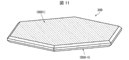
量子ドット300は、複数の結晶面を有する多面体の結晶であり、その表面が主に極性面である。量子ドット300は例えば、図11に示す六角形の(0001)面及び(000-1)面の2面を上面及び底面として含む[0001]方向に薄い平板形状である。
The quantum dot 300 is a polyhedral crystal having a plurality of crystal planes, the surfaces of which are mainly polar planes. The quantum dot 300 has, for example, a flat plate shape thin in the [0001] direction, which includes the (0001) plane and the (000-1) plane of the hexagon shown in FIG. 11 as the top and bottom surfaces.
図11は、量子ドット300の結晶面において、(0001)と等価な面を示す図である。図11において、(0001)面および(0001)面と等価な面には、ハッチング処理を施している。量子ドット300の結晶面のうち、(0001)面と等価な面は、(0001)面の反対側の(000-1)面である。
FIG. 11 is a diagram showing a plane equivalent to (0001) in the crystal plane of the quantum dot 300. FIG. In FIG. 11, the (0001) plane and planes equivalent to the (0001) plane are hatched. Of the crystal planes of the quantum dot 300, the plane equivalent to the (0001) plane is the (000-1) plane opposite to the (0001) plane.
ウルツ鉱型結晶における(0001)等価面および(1-101)等価面は極性面である。量子ドット300において(1-101)等価面は、(1-101)面、(01-11)面、(-1011)面、(-1101)面、(0-111)面、(10-11)面、(1-10-1)面、(01-1-1)面、(-101-1)面、(-110-1)面、(0-11-1)面、(10-1-1)面、の12面である。本実施形態3に係る量子ドット300の表面も、前述の実施形態1と同様に、面積比70%以上が極性面であればよく、80%以上が極性面であることが好ましく、90%以上が極性面であることがより好ましい。また、量子ドット300が平板形状であることが理想的である。
The (0001) equivalent plane and (1-101) equivalent plane in wurtzite crystals are polar planes. In the quantum dot 300, the (1-101) equivalent plane is the (1-101) plane, (01-11) plane, (-1011) plane, (-1101) plane, (0-111) plane, (10-11 ) plane, (1-10-1) plane, (01-1-1) plane, (-101-1) plane, (-110-1) plane, (0-11-1) plane, (10-1 −1) plane, 12 planes. The surface of the quantum dot 300 according to Embodiment 3 may be a polar surface with an area ratio of 70% or more, preferably 80% or more, as in Embodiment 1 described above, and preferably 90% or more. is more preferably a polar face. Also, it is ideal that the quantum dot 300 has a flat plate shape.
前述の実施形態1と同様に、量子ドット300の結晶面分析の結果において算出された極性面の面積比が90%以上であれば、発光層54には表面の100%が極性面である量子ドット300を含んでいると考えられる。
As in the first embodiment described above, if the area ratio of the polar plane calculated in the result of the crystal plane analysis of the quantum dot 300 is 90% or more, the light-emitting layer 54 has quantum dots in which 100% of the surface is a polar plane. Dot 300 is considered to be included.
量子ドット300の上面と底面との間の面は、非極性面を含んでもよく、例えば、(1-100)等価面を含んでよい。量子ドット300において(1-100)等価面は、(1-100)面、(01-10)面、(-1010)面、(-1100)面、(0-110)面、(10-10)面、の6面である。量子ドット300の上面と底面との間の面は、極性面を含むことが好ましく、例えば、(0001)等価面に対して傾斜している(1-101)等価面を含むことが好ましい。量子ドット300の上面と底面との間の面は、非極性面と極性面との双方または片方のみを含んでもよい。
A plane between the top and bottom surfaces of the quantum dot 300 may include a non-polar plane, for example, a (1-100) equivalent plane. In the quantum dot 300, the (1-100) equivalent plane is the (1-100) plane, (01-10) plane, (-1010) plane, (-1100) plane, (0-110) plane, (10-10 ) face. The plane between the top and bottom surfaces of the quantum dot 300 preferably includes a polar plane, eg, a (1-101) equivalent plane that is tilted with respect to the (0001) equivalent plane. The planes between the top and bottom surfaces of quantum dots 300 may include non-polar and/or polar planes.
図10に示すように、量子ドット300は、当該量子ドット300の表面における(0001)等価面の面積の割合が大きいために、[0001]方向に薄い平板形状を有する。このため、量子ドット300における励起子の再結合の方向は、主に、[0001]方向に略垂直な方向である。これによって、励起子の再結合によって放出される光は、[0001]方向に略平行な方向に強く放出される。発光層54の形成時に、量子ドット300は、自重により、量子ドット300の(0001)等価面の何れかが、発光層54の上面側または底面側に位置するように堆積しやすい。これらの結果、自発光素子5において発光層54は光を主に、発光層54の上面および底面に略直交する方向に放射する。このため、入射角が小さいので、放射された光が自発光素子5における境界面で反射され難くなり、自発光素子5内部での光の減衰が低減される。これによって、自発光素子5から光を取出す効率が向上する。
As shown in FIG. 10, the quantum dot 300 has a thin plate shape in the [0001] direction because the proportion of the area of the (0001) equivalent plane on the surface of the quantum dot 300 is large. Therefore, the direction of recombination of excitons in the quantum dot 300 is mainly the direction substantially perpendicular to the [0001] direction. As a result, light emitted by recombination of excitons is strongly emitted in a direction substantially parallel to the [0001] direction. During the formation of the light-emitting layer 54 , the quantum dots 300 tend to deposit due to their own weight such that one of the (0001) equivalent planes of the quantum dots 300 is positioned on the top side or the bottom side of the light-emitting layer 54 . As a result, the light-emitting layer 54 in the self-light-emitting element 5 mainly emits light in a direction substantially orthogonal to the top surface and bottom surface of the light-emitting layer 54 . Therefore, since the incident angle is small, the radiated light is less likely to be reflected at the boundary surface of the self-luminous element 5, and the attenuation of the light inside the self-luminous element 5 is reduced. This improves the efficiency of extracting light from the self-luminous element 5 .
(量子ドットの製造方法)
本実施形態3に係る量子ドット300の製法は、前述の実施形態1と同様に、例えば、加熱法、ホットインジェクション、マイクロ波アシスト法、連続フロー法、がある。
(Method for manufacturing quantum dots)
The method of manufacturing the quantum dots 300 according to the third embodiment includes, for example, a heating method, a hot injection method, a microwave assisted method, and a continuous flow method, as in the first embodiment described above.
図12および図13は各々、図10に示した量子ドット300の一例の製造方法を示す図である。
12 and 13 are diagrams each showing an example manufacturing method of the quantum dot 300 shown in FIG.
図10に示すような平板形状かつウルツ鉱型の量子ドット300は、ウルツ鉱型の結晶系を有する材料をシート状に作成し、必要に応じてイオンを置換することによって製造できる。例えば、量子ドット300がCdSeから成る場合、まず、CdCl2にオレイルアミン(図12にOAで示す)を添加することによって、CdCl2のナノシート状の錯体を形成する。CdCl2は、ウルツ鉱型の結晶系を通常有する材料である。
A flat plate-shaped wurtzite quantum dot 300 as shown in FIG. 10 can be manufactured by forming a material having a wurtzite crystal system into a sheet and substituting ions as necessary. For example, if the quantum dots 300 are composed of CdSe, the nanosheet-like complexes of CdCl 2 are first formed by adding oleylamine (shown as OA in FIG. 12) to CdCl 2 . CdCl2 is a material that normally has a wurtzite crystal system.
続いて、Seを融解したオクチルアミン溶液を、前述のCdCl2錯体と混和し、摂氏100度で24時間反応させる。この結果、図13に示すように、2つの塩化物イオンCl-が1つのセレン化物イオンSe-に置換されて、CdSeのナノシート状の錯体を形成する。このように形成されたCdSeは、平板形状かつウルツ鉱型の結晶系を有する。
Subsequently, the Se melted octylamine solution is mixed with the aforementioned CdCl 2 complex and reacted at 100 degrees Celsius for 24 hours. As a result, as shown in FIG. 13, two chloride ions Cl − are replaced by one selenide ion Se − to form a CdSe nanosheet complex. The CdSe thus formed has a tabular and wurtzite crystal system.
(変形例)
図14は、本実施形態3に係る量子ドット300の変形例の構造を示す斜視図である。
(Modification)
FIG. 14 is a perspective view showing the structure of a modification of the quantum dot 300 according to Embodiment 3. FIG.
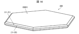
量子ドット300の上面と底面との間の面は、非極性面として、例えば、図14に示すように(11-20)面および(11-20)面と等価な面を含んでもよい。量子ドット300の上面と底面との間の面は、極性面として、例えば、(11-21)面および(11-21)と等価な面を含んでもよい。(11-20)と等価な面は、(-2110)面、(1-210)面、(-1-120)面、(2-1-10)面、及び(-12-10)面、である。(11-21)と等価な面は、(-2111)面、(1-211)面、(-1-121)面、(2-1-11)面、(-12-11)、(-2111)面、(11-2-1)面、(1-21-1)面、(-1-12-1)面、(2-1-1-1)面、及び(-12-1-1)面である。
The plane between the top and bottom surfaces of the quantum dot 300 may include, for example, the (11-20) plane and a plane equivalent to the (11-20) plane as shown in FIG. 14 as non-polar planes. The planes between the top and bottom surfaces of the quantum dot 300 may include, for example, the (11-21) plane and planes equivalent to the (11-21) as polar planes. The planes equivalent to (11-20) are the (-2110) plane, (1-210) plane, (-1-120) plane, (2-1-10) plane, and (-12-10) plane, is. The planes equivalent to (11-21) are the (-2111) plane, (1-211) plane, (-1-121) plane, (2-1-11) plane, (-12-11), (- 2111) plane, (11-2-1) plane, (1-21-1) plane, (-1-12-1) plane, (2-1-1-1) plane, and (-12-1- 1) It is a face.
以降、(11-20)面および(11-20)面と等価な面を包括して、(11-20)等価面と総称し、(11-21)面および(11-21)と等価な面を包括して(11-21)等価面と総称する。
Hereinafter, the (11-20) plane and a plane equivalent to the (11-20) plane are collectively referred to as the (11-20) equivalent plane, and The faces are collectively referred to as (11-21) equivalent faces.
本実施形態3も、前述の実施形態1と同様に、太陽電池に適用可能である。
The third embodiment can also be applied to solar cells as in the first embodiment.
〔実施形態4〕
本発明の他の実施形態について、以下に説明する。なお、説明の便宜上、上記実施形態にて説明した部材と同じ機能を有する部材については、同じ符号を付記し、その説明を繰り返さない。
[Embodiment 4]
Other embodiments of the invention are described below. For convenience of description, members having the same functions as those of the members described in the above embodiments are denoted by the same reference numerals, and description thereof will not be repeated.
本実施形態4に係る発光層54(図1参照)は、前述の実施形態1に係る量子ドット100および極性リガンド2の代わりに、本実施形態4に係る量子ドット400および中性リガンド3を含む点においてのみ、前述の実施形態1に係る自発光素子5から異なる。
The light-emitting layer 54 (see FIG. 1) according to Embodiment 4 includes the quantum dots 400 and neutral ligands 3 according to Embodiment 4 instead of the quantum dots 100 and polar ligands 2 according to Embodiment 1 described above. It differs from the self-luminous element 5 according to the first embodiment described above only in this point.
(量子ドットの構造)
図15は本実施形態4に係る量子ドット400の一例の構造を示す斜視図である。図16は、図15に示した量子ドット400の表面と、当該表面を保護する中性リガンド3とを概略的に示す模式図である。
(Structure of quantum dots)
FIG. 15 is a perspective view showing an example structure of the quantum dot 400 according to the fourth embodiment. FIG. 16 is a schematic diagram schematically showing the surface of the quantum dot 400 shown in FIG. 15 and the neutral ligand 3 protecting the surface.
本実施形態4に係る量子ドット400は、閃亜鉛鉱型の結晶系を有する。量子ドット400は、閃亜鉛鉱型の結晶系を自発的に取り得る材料を含む群から選択される少なくとも1つを含むことが好ましい。当該材料は例えば、ZnS,CdSe,ZnSeなどのII―VI族化合物および、InPなどのIII-V族化合物である。
The quantum dot 400 according to Embodiment 4 has a zinc blende crystal system. Quantum dot 400 preferably includes at least one selected from the group including materials capable of spontaneously adopting a zinc blende crystal system. Such materials are, for example, II-VI compounds such as ZnS, CdSe, ZnSe and III-V compounds such as InP.
本実施形態4に係る量子ドット400がコアシェル構造を有する場合、前述の実施形態1と同様に、コアのバンドギャップはシェルのバンドギャップよりも小さいことが好ましい。
When the quantum dot 400 according to Embodiment 4 has a core-shell structure, the core bandgap is preferably smaller than the shell bandgap, as in Embodiment 1 described above.
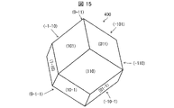
量子ドット400は、複数の結晶面を有する多面体の結晶であり、その表面が主に非極性面である。量子ドット400の表面は例えば、図15に示す菱形の(110)面、(011)面、(101)面、(1-10)面、(01-1)面、(-101)面、(-110)面、(0-11)面、(10-1)面、(-1-10)面、(0-1-1)面、(-10-1)面、の12面を含む。この場合、量子ドット400の理想的な形状は、十二面体である。量子ドット400の結晶面のうち、(110)面と等価な面は、(011)面、(101)面、(1-10)面、(01-1)面、(-101)面、(-110)面、(0-11)面、(10-1)面、(-1-10)面、(0-1-1)面、(-10-1)面である。
The quantum dot 400 is a polyhedral crystal having multiple crystal planes, the surfaces of which are mainly non-polar planes. The surface of the quantum dot 400 is, for example, the rhombic (110) plane, (011) plane, (101) plane, (1-10) plane, (01-1) plane, (-101) plane, (-101) plane, ( -110) plane, (0-11) plane, (10-1) plane, (-1-10) plane, (0-1-1) plane, and (-10-1) plane. In this case, the ideal shape of quantum dot 400 is a dodecahedron. Among the crystal planes of the quantum dot 400, planes equivalent to the (110) plane are the (011) plane, (101) plane, (1-10) plane, (01-1) plane, (−101) plane, ( −110) plane, (0-11) plane, (10-1) plane, (−1-10) plane, (0-1-1) plane, and (−10-1) plane.
閃亜鉛鉱型の結晶系における(110)等価面は、非極性面である。量子ドット400の表面が非極性面である場合、図16に示すように、中性リガンド3のみを用いて量子ドット400の表面を十分に保護(表面保護)できる。中性リガンド3は、非極性面に非共有電子対3aを介して結合できる。
The (110) equivalent plane in the sphalerite-type crystal system is a non-polar plane. When the surface of the quantum dot 400 is a non-polar plane, the surface of the quantum dot 400 can be sufficiently protected (surface protected) using only the neutral ligand 3, as shown in FIG. A neutral ligand 3 can bind to the non-polar surface via a lone pair of electrons 3a.
本実施形態4に係る量子ドット100の表面の70%以上が非極性面である場合、前述の実施形態1と類似の理由で、中性リガンド3のみを用いて量子ドット400の表面を十分に保護(表面保護)できる。
When 70% or more of the surface of the quantum dot 100 according to Embodiment 4 is a non-polar surface, for the same reason as in Embodiment 1 described above, the surface of the quantum dot 400 is sufficiently covered using only the neutral ligand 3. Can be protected (surface protection).
量子ドット400の表面における非極性面の面積比が高いほど、中性リガンド3による表面保護の効果が向上する。故に、本実施形態4に係る量子ドット400の表面は、前述の実施形態1と逆に、面積比70%以上が非極性面であればよく、80%以上が非極性面であることが好ましく、90%以上が非極性面であることがより好ましい。また、量子ドット400の表面が非極性面のみを含むことが理想的である。
The higher the area ratio of the non-polar planes on the surface of the quantum dot 400, the more effectively the surface is protected by the neutral ligand 3. Therefore, the surface of the quantum dot 400 according to Embodiment 4 may be a non-polar surface with an area ratio of 70% or more, and preferably 80% or more is a non-polar surface, contrary to the above-described Embodiment 1. , 90% or more of which are non-polar surfaces. Also, ideally, the surface of quantum dot 400 includes only non-polar planes.
前述の実施形態1と同様に、量子ドット400の結晶面分析の結果において算出された非極性面の面積比が60%以上であれば、発光層54に含まれる量子ドット400の少なくとも一部は中性リガンド3のみで十分に表面保護されると考えられる。また90%以上であれば、発光層54には表面の100%が非極性面である量子ドット400を含んでいると考えられる。
As in the first embodiment described above, if the area ratio of the nonpolar plane calculated in the result of the crystal plane analysis of the quantum dots 400 is 60% or more, at least part of the quantum dots 400 included in the light emitting layer 54 It is believed that neutral ligand 3 alone provides sufficient surface protection. Moreover, if it is 90% or more, it is considered that the light-emitting layer 54 contains the quantum dots 400 in which 100% of the surface is a non-polar plane.
非極性面は極性面と比較して、表面電荷が小さく、未結合手濃度が小さい。このため、非極性面は反応性が比較的低い傾向にあり、量子ドットの表面からリガンドが脱離したときに、非極性面は不純物などと比較的反応しにくい傾向にある。したがって、本実施形態4に係る量子ドット400は、劣化しにくいので、発光層54および自発光素子5の信頼性を向上できる。
A non-polar surface has a smaller surface charge and a smaller concentration of dangling bonds than a polar surface. For this reason, nonpolar surfaces tend to have relatively low reactivity, and when ligands are desorbed from the surface of quantum dots, nonpolar surfaces tend to react relatively poorly with impurities and the like. Therefore, since the quantum dots 400 according to the fourth embodiment are less likely to deteriorate, the reliability of the light-emitting layer 54 and the self-light-emitting element 5 can be improved.
中性リガンド3は、有機であり、例えば、末端に一つ以上のホスフィン基、ホスフィンオキシド基、及びアミン基を含む有機中性リガンドから成る群から選択される少なくとも1種を含む。末端にホスフィン基を含むリガンドは、下記構造式(8)または下記構造式(9)で表される構造を一部に含む。末端にホスフィンオキシド基を含むリガンドは、下記構造式(10)で表される構造を一部に含む。末端にアミン基を含むリガンドは、下記構造式(11)~(15)の何れか1つで表される構造を一部に含む。
The neutral ligand 3 is organic and includes, for example, at least one selected from the group consisting of organic neutral ligands containing one or more phosphine groups, phosphine oxide groups, and amine groups at the ends. A ligand containing a phosphine group at its terminal partly includes a structure represented by the following structural formula (8) or the following structural formula (9). A ligand containing a phosphine oxide group at its terminal partly includes a structure represented by the following structural formula (10). A ligand containing an amine group at its terminal partly includes a structure represented by any one of the following structural formulas (11) to (15).
なお、上記構造式(8)~(15)において、Hは水素原子を示し、Nは窒素原子を示し、Oは酸素原子を示し、Pはリン原子を示し、R1およびR2およびR3は、それぞれ独立して、水素原子、アルキル基、アリール基、アルコキシル基、または不飽和炭化水素基を示す。
In the structural formulas (8) to (15) above, H represents a hydrogen atom, N represents a nitrogen atom, O represents an oxygen atom, P represents a phosphorus atom, R 1 , R 2 and R 3 each independently represents a hydrogen atom, an alkyl group, an aryl group, an alkoxyl group, or an unsaturated hydrocarbon group.
(量子ドットの製造方法)
量子ドット400の製法としては、前述の実施形態1と同様に、例えば、加熱法、ホットインジェクション、マイクロ波アシスト法、連続フロー法、がある。
(Method for manufacturing quantum dots)
Methods for manufacturing the quantum dots 400 include, for example, a heating method, a hot injection method, a microwave assist method, and a continuous flow method, as in the first embodiment described above.
図15に示すような十二面体の量子ドットは、最外層の合成時に非極性面に優先的に結合する中性リガンドを用いて、製造できる。例えば、量子ドット400がCdSeから成る場合、中性リガンドを多めに添加して、250度程度の反応温度で結晶成長させる。中性リガンドは、アミン系リガンドが好ましい。アミン系リガンドはCdSeの(110)等価面への強く結合し、その他の面に弱く結合するか結合しない。この結果、(110)等価面以外の面で結晶成長が進み、量子ドット400の表面が(110)等価面で構成される。
A dodecahedral quantum dot as shown in FIG. 15 can be produced using a neutral ligand that preferentially binds to the non-polar face during synthesis of the outermost layer. For example, when the quantum dots 400 are made of CdSe, a large amount of neutral ligand is added and the crystal is grown at a reaction temperature of about 250 degrees. Neutral ligands are preferably amine-based ligands. Amine-based ligands bind strongly to the (110) equivalent face of CdSe and weakly or not to other faces. As a result, crystal growth progresses on planes other than the (110) equivalent plane, and the surface of the quantum dot 400 is composed of the (110) equivalent plane.
本実施形態4も、前述の実施形態1と同様に、太陽電池に適用可能である。
The fourth embodiment can also be applied to solar cells as in the first embodiment.
〔実施形態5〕
本発明の他の実施形態について、以下に説明する。なお、説明の便宜上、上記実施形態にて説明した部材と同じ機能を有する部材については、同じ符号を付記し、その説明を繰り返さない。
[Embodiment 5]
Other embodiments of the invention are described below. For convenience of description, members having the same functions as those of the members described in the above embodiments are denoted by the same reference numerals, and description thereof will not be repeated.
本実施形態5に係る発光層54(図1参照)は、前述の実施形態1に係る量子ドット100および極性リガンド2の代わりに、本実施形態5に係る量子ドット500および中性リガンド3を含む点においてのみ、前述の実施形態1に係る自発光素子5から異なる。
The light-emitting layer 54 (see FIG. 1) according to Embodiment 5 includes quantum dots 500 and neutral ligands 3 according to Embodiment 5 instead of the quantum dots 100 and polar ligands 2 according to Embodiment 1 described above. It differs from the self-luminous element 5 according to the first embodiment described above only in this respect.
(量子ドットの構造)
図17は本実施形態5に係る量子ドット500の一例の構造を示す斜視図である。
(Structure of quantum dots)
FIG. 17 is a perspective view showing an example structure of a quantum dot 500 according to the fifth embodiment.
本実施形態5に係る量子ドット500は、塩化ナトリウム型の結晶系を有する。量子ドット200は、塩化ナトリウム型の結晶系を自発的に取り得る材料を含む群から選択される少なくとも1つを含むことが好ましい。当該材料は例えば、PbTe,PbSe,PbSなどのIV―VI族化合物である。
The quantum dot 500 according to Embodiment 5 has a sodium chloride type crystal system. The quantum dot 200 preferably contains at least one selected from the group containing materials that can spontaneously assume a sodium chloride type crystal system. The material is, for example, a IV-VI group compound such as PbTe, PbSe, PbS.
本実施形態5に係る量子ドット500がコアシェル構造を有する場合、前述の実施形態1と同様に、コアのバンドギャップはシェルのバンドギャップよりも小さいことが好ましい。
When the quantum dot 500 according to Embodiment 5 has a core-shell structure, the core bandgap is preferably smaller than the shell bandgap, as in Embodiment 1 described above.
量子ドット500は、複数の結晶面を有する多面体の結晶であり、その表面が主に非極性面である。量子ドット500の表面は例えば、図17に示す四角形の(100)等価面、(-100)面、(010)面、(0-10)面、(001)面、及び(00-1)面の6面を含む。これら6面は、(100)等価面である。この場合、量子ドット500の理想的な形状は、直方体である。
The quantum dot 500 is a polyhedral crystal having a plurality of crystal planes, the surfaces of which are mainly non-polar planes. The surface of the quantum dot 500 is, for example, the quadrangular (100) equivalent plane, (−100) plane, (010) plane, (0-10) plane, (001) plane, and (00-1) plane shown in FIG. including six sides of These six faces are (100) equivalent faces. In this case, the ideal shape of quantum dot 500 is a cuboid.
塩化ナトリウム型の結晶系における(100)等価面は、非極性面である。本実施形態5に係る量子ドット500の表面も、前述の実施形態4と同様に、面積比70%以上が非極性面であればよく、80%以上が非極性面であることが好ましく、90%以上が非極性面であることがより好ましい。また、量子ドット500の表面が非極性面のみを含むことが理想的である。
The (100) equivalent plane in the sodium chloride type crystal system is a non-polar plane. The surface of the quantum dot 500 according to Embodiment 5 may be a nonpolar surface with an area ratio of 70% or more, preferably 80% or more, as in Embodiment 4 described above. % or more are non-polar planes. Also, ideally, the surface of quantum dot 500 includes only non-polar planes.
前述の実施形態1と同様に、量子ドット500の結晶面分析の結果において算出された非極性面の面積比が90%以上であれば、発光層54にはの表面の100%が非極性面である量子ドット500を含んでいると考えられる。
As in the first embodiment described above, if the area ratio of the non-polar planes calculated in the crystal plane analysis results of the quantum dots 500 is 90% or more, 100% of the surface of the light-emitting layer 54 is non-polar planes. is believed to contain quantum dots 500 that are
(量子ドットの製造方法)
本実施形態5に係る量子ドット500の製法は、前述の実施形態1と同様に、例えば、加熱法、ホットインジェクション、マイクロ波アシスト法、連続フロー法、がある。
(Method for manufacturing quantum dots)
The method of manufacturing the quantum dots 500 according to the fifth embodiment includes, for example, a heating method, a hot injection method, a microwave assisted method, and a continuous flow method, as in the first embodiment described above.
図17に示すような六面体の量子ドット500は、非特許文献1に記載の製造方法に加えて、最外層の合成時に非極性面に優先的に結合する中性リガンド(アミン系リガンド)を用いて、反応温度を低くすることによって、製造できる。例えば、量子ドット100がPbSから成る場合、摂氏110度程度で結晶成長させる。
A hexahedral quantum dot 500 as shown in FIG. 17 uses a neutral ligand (amine-based ligand) that preferentially binds to a non-polar surface when synthesizing the outermost layer, in addition to the manufacturing method described in Non-Patent Document 1. can be produced by lowering the reaction temperature. For example, when the quantum dots 100 are made of PbS, crystal growth is performed at about 110 degrees Celsius.
本実施形態5も、前述の実施形態1と同様に、太陽電池に適用可能である。
The fifth embodiment can also be applied to solar cells as in the first embodiment.
〔実施形態6〕
本発明の他の実施形態について、以下に説明する。なお、説明の便宜上、上記実施形態にて説明した部材と同じ機能を有する部材については、同じ符号を付記し、その説明を繰り返さない。
[Embodiment 6]
Other embodiments of the invention are described below. For convenience of description, members having the same functions as those of the members described in the above embodiments are denoted by the same reference numerals, and description thereof will not be repeated.
本実施形態6に係る自発光素子5(図1参照)は、発光層54が、前述の実施形態1に係る量子ドット100および極性リガンド2の代わりに、本実施形態6に係る量子ドット600および中性リガンド3を含む点においてのみ、前述の実施形態1に係る自発光素子5から異なる。
In the self-luminous device 5 (see FIG. 1) according to the sixth embodiment, the light-emitting layer 54 is the quantum dots 600 and the quantum dots 600 according to the sixth embodiment instead of the quantum dots 100 and the polar ligands 2 according to the first embodiment It differs from the self-luminous element 5 according to the first embodiment described above only in that the neutral ligand 3 is included.
(量子ドットの構造)
図18は本実施形態6に係る量子ドット600の構造を示す斜視図である。図19は、図18に示した量子ドット600の各結晶面の面方位を示す図である。
(Structure of quantum dots)
FIG. 18 is a perspective view showing the structure of a quantum dot 600 according to Embodiment 6. FIG. FIG. 19 is a diagram showing the plane orientation of each crystal plane of the quantum dot 600 shown in FIG.
本実施形態6に係る量子ドット600は、ウルツ鉱型の結晶系を有する。量子ドット600は、ウルツ鉱型の結晶系を自発的に取り得る材料を含む群から選択される少なくとも1つを含むことが好ましい。当該材料は例えば、ZnS,CdSe,ZnSeなどのII―VI族化合物である。なお、II―VI族化合物は結晶成長条件によって、閃亜鉛鉱型の結晶系も取り得る。
The quantum dot 600 according to Embodiment 6 has a wurtzite crystal system. Quantum dot 600 preferably includes at least one selected from the group including materials capable of spontaneously adopting a wurtzite crystal system. The material is, for example, a II-VI group compound such as ZnS, CdSe, ZnSe. Depending on the crystal growth conditions, the group II-VI compound can also take a zincblende crystal system.
量子ドット600は、複数の結晶面を有する多面体の結晶であり、その表面が主に極性面である。量子ドット600は例えば、図19に示す長方形の(1-100)面、(0-110)面、(-1010)面、(-1100)面、(01-10)面、及び(10-10)面の6面を側面として含む[0001]方向に細長い棒状である。棒の形状は、六角柱形状及び、六角柱の1つ以上の角を切り取った形状を含む。
The quantum dot 600 is a polyhedral crystal having a plurality of crystal planes, the surfaces of which are mainly polar planes. Quantum dots 600 are, for example, rectangular (1-100) planes, (0-110) planes, (-1010) planes, (-1100) planes, (01-10) planes, and (10-10) planes shown in FIG. ) in the direction of [0001] including 6 faces as side faces. Bar shapes include hexagonal prism shapes and shapes obtained by truncating one or more corners of hexagonal prisms.
図19は、量子ドット600の結晶面において、(1-100)面と等価な面を示す図である。図19において、(1-100)面および(1-100)面と等価な面には、ハッチング処理を施している。量子ドット600の結晶面のうち、(1-100)面と等価な面は、(0-110)面、(-1010)面、(-1100)面、(01-10)面、及び(10-10)である。
FIG. 19 is a diagram showing a plane equivalent to the (1-100) plane among the crystal planes of the quantum dot 600. FIG. In FIG. 19, the (1-100) plane and planes equivalent to the (1-100) plane are hatched. Among the crystal planes of the quantum dot 600, the planes equivalent to the (1-100) plane are the (0-110) plane, (-1010) plane, (-1100) plane, (01-10) plane, and (10 -10).
ウルツ鉱型結晶における(-1100)等価面は非極性面である。本実施形態6に係る量子ドット600の表面も、前述の実施形態4と同様に、面積比70%以上が非極性面であればよく、80%以上が非極性面であることが好ましく、90%以上が非極性面であることがより好ましい。また、量子ドット600の表面が非極性面のみを含むことが理想的である。
The (-1100) equivalent plane in the wurtzite crystal is a non-polar plane. The surface of the quantum dot 600 according to Embodiment 6 may be a non-polar surface with an area ratio of 70% or more, preferably 80% or more, as in Embodiment 4 described above. % or more are non-polar planes. Also, ideally, the surface of quantum dot 600 includes only non-polar planes.
前述の実施形態1と同様に、量子ドット600の結晶面分析の結果において算出された非極性面の面積比が90%以上であれば、発光層54には量子ドット600の表面の100%が非極性面である量子ドット600を含んでいると考えられる。
As in Embodiment 1 described above, if the area ratio of the nonpolar plane calculated in the result of the crystal plane analysis of the quantum dots 600 is 90% or more, 100% of the surface of the quantum dots 600 is in the light emitting layer 54. It is believed to contain quantum dots 600, which are non-polar planes.
量子ドット600は、側面同士の一方側の間の面と、側面同士の他方側の間の面とが極性面であってもよく、例えば(0001)等価面および/または(1-101)等価面を含んでよい。
Quantum dot 600 may have a polar surface between one of its sides and a surface between the other of its sides, such as (0001) equivalence and/or (1-101) equivalence. May contain faces.
図18に示すように、量子ドット600は、当該量子ドット600の表面における(-1100)等価面の面積の割合が大きいために、[0001]方向に細長い棒状の形状を有する。このため、量子ドット600における励起子の再結合の方向は、主に、[0001方向]に略平行な方向である。これによって、励起子の再結合によって放出される光は、量子ドット600の[0001]方向に略垂直な方向に強く放出される。発光層54の形成時に、量子ドット600は、自重により、量子ドット600の(-1100)等価面の何れかが、発光層54の上面側または底面側に位置するように堆積しやすい。これらの結果、自発光素子5において発光層54は光を主に、発光層54の上面および底面に略直交する方向に放射する。このため、放射された光が自発光素子5における境界面で反射され難くなり、自発光素子5内部での光の減衰が低減される。これによって、自発光素子5から光を取出す効率が向上する。
As shown in FIG. 18, the quantum dot 600 has a rod-like shape elongated in the [0001] direction because the area of the (-1100) equivalent plane on the surface of the quantum dot 600 is large. Therefore, the recombination direction of excitons in the quantum dot 600 is mainly a direction substantially parallel to the [0001 direction]. As a result, light emitted by recombination of excitons is strongly emitted in a direction substantially perpendicular to the [0001] direction of the quantum dots 600 . When forming the light-emitting layer 54 , the quantum dots 600 tend to be deposited by their own weight so that either of the (−1100) equivalent planes of the quantum dots 600 is positioned on the top side or the bottom side of the light-emitting layer 54 . As a result, the light-emitting layer 54 in the self-light-emitting element 5 mainly emits light in a direction substantially perpendicular to the top surface and bottom surface of the light-emitting layer 54 . For this reason, the emitted light is less likely to be reflected at the interface of the self-luminous element 5, and the attenuation of light inside the self-luminous element 5 is reduced. This improves the efficiency of extracting light from the self-luminous element 5 .
(量子ドットの製造方法)
本実施形態6に係る量子ドット600の製法は、前述の実施形態1と同様に、例えば、加熱法、ホットインジェクション、マイクロ波アシスト法、連続フロー法、がある。
(Method for manufacturing quantum dots)
The manufacturing method of the quantum dot 600 according to the sixth embodiment includes, for example, a heating method, a hot injection method, a microwave assist method, and a continuous flow method, as in the first embodiment described above.
図18に示すような棒状かつウルツ鉱型の量子ドットは、コアとしてウルツ鉱型のナノ結晶を形成し、そのコアの(0001)等価面の上に、シェルとしてウルツ鉱型のナノ結晶をエピタキシャル成長させることによって製造できる。
Rod-shaped and wurtzite quantum dots, such as shown in FIG. 18, form a wurtzite nanocrystal as the core and epitaxially grow a wurtzite nanocrystal as the shell on the (0001) equivalent face of the core. It can be manufactured by
例えば、量子ドット600がCdSeのコアとCdSのシェルから成る場合、まず、三口フラスコを用意し、1.5mmolのCdO、6mmolのnテトラデシルホスホン酸(n-tetradecylphosphonic acid:TDPA)、24mmolのオレイルアルコール、および10gのTOPOを三つ口フラスコに入れて混合する。これを窒素環境下にて摂氏150度で1時間加熱する。その後、350度に向けて昇温させ、この溶液が透明になった瞬間にTOPをフラスコに2ml注入する。この溶液が摂氏350度に達したら、体積モル濃度1.7mol/lのSeのTOP錯体(trioctylphosphine selenide:TOP-Se)溶液をフラスコに1.5ml注入する。数秒間の反応後、フラスコを摂氏80度の水に浸すことで降温し、反応を停止させる。続いて、この溶液に20mlのメタノールを加え、ナノ粒子を沈殿させる。このナノ粒子は、CdSeのウルツ鉱型の結晶である。このCdSeのナノ結晶を、体積濃度2.4mol/lの硫化物TOP(trioctylphosphine sulfide:TOP-S)溶液に分散させる。
For example, if the quantum dot 600 consists of a CdSe core and a CdS shell, first prepare a three-neck flask, 1.5 mmol CdO, 6 mmol n-tetradecylphosphonic acid (TDPA), 24 mmol oleyl Mix the alcohol and 10 g of TOPO in a 3-necked flask. It is heated at 150 degrees Celsius for 1 hour in a nitrogen environment. After that, the temperature is raised to 350° C., and 2 ml of TOP is injected into the flask at the moment when this solution becomes transparent. When the solution reaches 350 degrees Celsius, 1.5 ml of a 1.7 mol/l molar concentration of Se TOP complex (trioctylphosphine selenide: TOP-Se) solution is injected into the flask. After reacting for several seconds, the temperature is lowered by immersing the flask in water at 80°C to stop the reaction. Subsequently, 20 ml of methanol is added to this solution to precipitate the nanoparticles. The nanoparticles are wurtzite crystals of CdSe. The CdSe nanocrystals are dispersed in a sulfide TOP (trioctylphosphine sulfide: TOP-S) solution with a volume concentration of 2.4 mol/l.
続いて、三口フラスコを用意し、5gのTOPO、任意量のオクタデシルホスホン酸(octadecylphosphonic acid:ODPA)、任意量のドデシルホスホン酸(dodecylphosphonic acid:DDPA)、および任意量のCdOをフラスコに入れて混合する。これを窒素環境下にて摂氏150度で1時間加熱する。その後、350度に向けて昇温させ、この溶液が透明になった瞬間にTOPをフラスコに1ml注入する。この溶液が摂氏350度に達したら、前述のCdSeナノ結晶をTOP-Sに分散させた溶液をフラスコに2ml注入する。なおここで、CdとSとのモル比率を1.2:1に維持することによって、CdS結晶がカチオンリッチの面を露出しやすいように留意する。十分な時間の反応後、フラスコを摂氏80度の水に浸すことで降温し、反応を停止させる。続いて、この溶液に5mlのトルエンおよび10mlのメタノールを加え、ナノロッドを沈殿させる。このナノロッドが量子ドット600である。
Next, prepare a three-necked flask, add 5 g of TOPO, an arbitrary amount of octadecylphosphonic acid (ODPA), an arbitrary amount of dodecylphosphonic acid (DDPA), and an arbitrary amount of CdO in the flask and mix. do. It is heated at 150 degrees Celsius for 1 hour in a nitrogen environment. After that, the temperature is raised to 350° C., and 1 ml of TOP is injected into the flask at the moment when this solution becomes transparent. When this solution reaches 350 degrees Celsius, 2 ml of the above-mentioned solution of CdSe nanocrystals dispersed in TOP-S is injected into the flask. It should be noted here that by maintaining the molar ratio of Cd and S at 1.2:1, the CdS crystal tends to expose the cation-rich surface. After a sufficient reaction time, the flask is immersed in water at 80 degrees Celsius to lower the temperature and stop the reaction. Subsequently, 5 ml of toluene and 10 ml of methanol are added to this solution to precipitate the nanorods. This nanorod is the quantum dot 600 .
(変形例)
図20および図22は各々、本実施形態6に係る量子ドット600の変形例の構造を示す斜視図である。図21は、図20に示した量子ドット600の各結晶面の面方位を示す図である。図23は各々、図22に示した量子ドット600の各結晶面の面方位を示す横断面図である。
(Modification)
20 and 22 are perspective views showing structures of modifications of the quantum dot 600 according to the sixth embodiment. FIG. 21 is a diagram showing the plane orientation of each crystal plane of the quantum dot 600 shown in FIG. 23A and 23B are cross-sectional views showing plane orientations of crystal planes of the quantum dot 600 shown in FIG.
本実施形態6に係る量子ドット600は、上述に限らない。
The quantum dot 600 according to Embodiment 6 is not limited to the above.
量子ドット600は例えば、図20および図21に示す長方形の(11-20)面、(-2110)面、(1-210)面、(-1-120)面、(2-1-10)面、及び(-12-10)面の6面を側面として含む細長い棒状であってもよい。(11-20)面と等価な面は、(-2110)面、(1-210)面、(-1-120)面、(2-1-10)面、及び(-12-10)面である。この場合、量子ドット600は、側面同士の一方側の間の面と、側面同士の他方側の間の面とが、例えば(0001)等価面および/または(11-21)等価面を含んでよい。
Quantum dots 600 are, for example, rectangular (11-20) planes, (-2110) planes, (1-210) planes, (-1-120) planes, (2-1-10) planes shown in FIGS. It may be in the shape of an elongated rod including six sides of a plane and a (-12-10) plane. The planes equivalent to the (11-20) plane are the (-2110) plane, (1-210) plane, (-1-120) plane, (2-1-10) plane, and (-12-10) plane. is. In this case, the quantum dot 600 has a surface between one side and a surface between the other side including, for example, a (0001) equivalent plane and/or a (11-21) equivalent plane. good.
図21は、図20に示した量子ドット600の結晶面において、(11-20)等価面を示す図である。
FIG. 21 is a diagram showing the (11-20) equivalent plane in the crystal plane of the quantum dot 600 shown in FIG.
ウルツ鉱型結晶において、(11-20)等価面は非極性面である。
In wurtzite crystals, the (11-20) equivalent plane is a nonpolar plane.
量子ドット600は例えば、図22に示すように、(1-100)等価面と(11-20)等価面との12面を側面として含む長い棒状であってもよい。この場合、棒の形状は十二角柱形状及び、十二角柱の1つ以上の角を切り取った形状を含む。図23は、図22に示した量子ドット600の横断面図である。この場合、量子ドット600は、側面同士の一方側の間の面と、側面同士の他方側の間の面とが、例えば(0001)等価面を含んでもよく、加えて/あるいは(1-101)等価面および(11-21)等価面を含んでよい。
For example, as shown in FIG. 22, the quantum dot 600 may be in the shape of a long rod including 12 sides of the (1-100) equivalent plane and the (11-20) equivalent plane. In this case, the rod shape includes a dodecagonal prism shape and a shape obtained by truncating one or more corners of a dodecagonal prism. FIG. 23 is a cross-sectional view of quantum dot 600 shown in FIG. In this case, the quantum dot 600 may include, for example, (0001) equivalent planes between the plane between one side of the sides and the plane between the other side of the sides, and/or (1-101 ) equivalent surface and (11-21) equivalent surface.
本実施形態6も、前述の実施形態1と同様に、太陽電池に適用可能である。
The sixth embodiment can also be applied to solar cells as in the first embodiment.
〔まとめ〕
本発明の態様1に係る量子ドットは、表面の面積比70%以上が極性面であるか、または、表面の面積比70%以上が非極性面である構成である。
〔summary〕
The quantum dot according to aspect 1 of the present invention has a structure in which 70% or more of the surface area is a polar plane, or 70% or more of the surface area is a non-polar plane.
なお、上記態様1における「面積比」は、実際の値である。上述したように、分析結果において、前記極性面(あるいは前記非極性面)が占める割合が60%以上であれば、発光層全体には極性面(あるいは非極性面)の面積比が70%以上の量子ドットが含まれると考えられる。したがって、分析結果における極性面(あるいは非極性面)の面積比が60%以上のとき、量子ドット層に含まれる量子ドットの少なくとも一部は、極性リガンド(あるいは中性リガンド)のみで十分に表面保護されると考えられる。
It should be noted that the "area ratio" in aspect 1 above is an actual value. As described above, if the ratio of the polar plane (or the non-polar plane) is 60% or more in the analysis result, the area ratio of the polar plane (or the non-polar plane) is 70% or more in the entire light-emitting layer. of quantum dots are considered to be included. Therefore, when the area ratio of the polar plane (or non-polar plane) in the analysis result is 60% or more, at least a part of the quantum dots contained in the quantum dot layer has a sufficient surface with only the polar ligand (or neutral ligand). considered protected.
本発明の態様2に係る量子ドットは、前記態様1において、前記表面は極性面のみまたは非極性面のみを含む構成であってもよい。
In the quantum dot according to aspect 2 of the present invention, in aspect 1, the surface may include only polar faces or only non-polar faces.
なお、上述したように、分析結果において、前記極性面(あるいは前記非極性面)が占める割合が90%以上であれば、実際に量子ドット層が量子ドットの表面の面積比100%が前記極性面(あるいは前記非極性面)である量子ドットを含んでいると考えられる。
As described above, if the ratio of the polar plane (or the non-polar plane) to the surface of the quantum dot layer is 90% or more in the analysis result, the quantum dot layer actually has an area ratio of 100% of the surface of the quantum dot. It is believed to contain quantum dots that are planes (or said non-polar planes).
本発明の態様3に係る量子ドットは、前記態様1または2において、コアシェル構造を有し、コアのバンドギャップは、シェルのバンドギャップよりも小さい構成であってもよい。
The quantum dot according to aspect 3 of the present invention may have a core-shell structure in aspect 1 or 2, and the bandgap of the core may be smaller than the bandgap of the shell.
本発明の態様4に係る量子ドットは、前記態様1~3の何れか1態様において、閃亜鉛鉱型の結晶系を有し、前記表面は、(100)面、(-100)面、(010)面、(0-10)面、(001)面、及び(00-1)面と、(111)面、(-111)面、(1-11)面、(-1-11)面、(11-1)面、(-11-1)面、(1-1-1)面、及び(-1-1-1)面と、の14面を含む構成であってもよい。
The quantum dot according to aspect 4 of the present invention, in any one aspect of aspects 1 to 3, has a zinc blende crystal system, and the surface is a (100) plane, a (−100) plane, ( 010) plane, (0-10) plane, (001) plane, and (00-1) plane, (111) plane, (-111) plane, (1-11) plane, (-1-11) plane , (11-1) plane, (-11-1) plane, (1-1-1) plane, and (-1-1-1) plane.
本発明の態様5に係る量子ドットは、前記態様1~3の何れか1態様において、閃亜鉛鉱型の結晶系を有し、前記表面は、(100)面、(-100)面、(010)面、(0-10)面、(001)面、及び(00-1)面の6面を含む構成であってもよい。
The quantum dot according to aspect 5 of the present invention, in any one aspect of aspects 1 to 3, has a zinc blende crystal system, and the surface is a (100) plane, a (−100) plane, ( 010) plane, (0-10) plane, (001) plane, and (00-1) plane.
本発明の態様6に係る量子ドットは、前記態様1~3の何れか1態様において、閃亜鉛鉱型の結晶系を有し、前記表面は、(111)面、(-111)面、(1-11)面、(-1-11)面、(11-1)面、(-11-1)面、(1-1-1)面、及び(-1-1-1)面と、の8面を含む構成であってもよい。
The quantum dot according to aspect 6 of the present invention, in any one aspect of aspects 1 to 3, has a zincblende crystal system, and the surfaces are (111) plane, (−111) plane, ( 1-11) plane, (-1-11) plane, (11-1) plane, (-11-1) plane, (1-1-1) plane, and (-1-1-1) plane, It may be a configuration including eight surfaces of.
本発明の態様7に係る量子ドットは、前記態様1~3の何れか1態様において、塩化ナトリウム型の結晶系を有し、前記表面は、(111)面、(-111)面、(1-11)面、(-1-11)面、(11-1)面、(-11-1)面、(1-1-1)面、及び(-1-1-1)面と、の8面を含む構成であってもよい。
The quantum dot according to aspect 7 of the present invention, in any one aspect of aspects 1 to 3, has a sodium chloride type crystal system, and the surfaces are (111) plane, (−111) plane, (1 -11) plane, (-1-11) plane, (11-1) plane, (-11-1) plane, (1-1-1) plane, and (-1-1-1) plane, A configuration including eight surfaces may be used.
本発明の態様8に係る量子ドットは、前記態様1~3の何れか1態様において、ウルツ鉱型の結晶系を有し、前記表面は、(0001)面及び(000-1)面の2面を含む構成であってもよい。
The quantum dot according to aspect 8 of the present invention, in any one aspect of aspects 1 to 3, has a wurtzite crystal system, and the surface is two of the (0001) plane and the (000-1) plane It may be a configuration including a plane.
本発明の態様9に係る量子ドット層は、前記態様4~8の何れか1態様に係る量子ドットと、極性リガンドとを含む構成である。
The quantum dot layer according to aspect 9 of the present invention has a configuration including the quantum dots according to any one aspect of aspects 4 to 8 and a polar ligand.
本発明の態様10に係る量子ドット層は、前記態様9において、当該量子ドット層に含まれるリガンドの物質量比90%以上が前記極性リガンドである構成であってもよい。
The quantum dot layer according to aspect 10 of the present invention, in aspect 9, may have a structure in which 90% or more of the substance amount of ligands contained in the quantum dot layer is the polar ligand.
なお、上記態様10における「物質量比」は、分析結果である。上述したように、分析結果において前記極性リガンドが占める割合が90%以上であれば、実際に量子ドットに含まれるリガンドの物質量比100%が前記極性リガンドである蓋然性が高いと考えられる。
It should be noted that the "substance amount ratio" in aspect 10 above is the analysis result. As described above, if the ratio of the polar ligands in the analysis results is 90% or more, it is highly probable that 100% of the ligands actually contained in the quantum dots are the polar ligands.
本発明の態様11に係る量子ドット層は、前記態様9または10において、前記極性リガンドは、下記構造式(1)~(7)で表される構造の少なくとも1つを少なくとも一部に含む構成であってもよい。
In the quantum dot layer according to aspect 11 of the present invention, in aspect 9 or 10, the polar ligand has at least one of the structures represented by the following structural formulas (1) to (7). may be
式中、Cは炭素原子を示し、Oは酸素原子を示し、O-は酸化物イオンを示し、Sは硫黄原子を示し、S-は硫化物イオンを示し、Pはリンを示し、R1およびR2は、それぞれ独立して、水素原子、アルキル基、アリール基、アルコキシル基、または不飽和炭化水素基を示す。
In the formula, C represents a carbon atom, O represents an oxygen atom, O - represents an oxide ion, S represents a sulfur atom, S - represents a sulfide ion, P represents phosphorus, R1 and Each R2 independently represents a hydrogen atom, an alkyl group, an aryl group, an alkoxyl group, or an unsaturated hydrocarbon group.
本発明の態様12に係る量子ドット層は、前記態様9または10において、前記極性リガンドは、イオン式Cl-、Br-、I-、SCN-、CN-、OH-、SH-、SeH-、TeH-、Se2-、S2-、Te2-、Sn2S6
4-、Sn2Se6
4-、In2Se4
2-、In2Te4
2-、Ga2Se4
2-、Sb2Se4
2-、Sb2Te4
2-で表される無機極性リガンドから成る群から選択される少なくとも1種を含む構成であってもよい。
In the quantum dot layer according to aspect 12 of the present invention, in aspect 9 or 10, the polar ligand has the ionic formula Cl − , Br − , I − , SCN − , CN − , OH − , SH − , SeH − , TeH − , Se 2− , S 2− , Te 2− , Sn 2 S 6 4− , Sn 2 Se 6 4− , In 2 Se 4 2− , In 2 Te 4 2− , Ga 2 Se 4 2− , The structure may include at least one selected from the group consisting of inorganic polar ligands represented by Sb 2 Se 4 2- and Sb 2 Te 4 2- .
本発明の態様13に係る量子ドットは、前記態様1~3の何れか1態様において、閃亜鉛鉱型の結晶系を有し、前記表面は、(101)面、(-101)面、(011)面、(0-11)面、(110)面、(-110)面、(1-1-)面、(-1-10)面、(10-1)面、(-10-1)面、(01-1)面、及び(0-1-1)面の12面を含む構成であってもよい。
The quantum dot according to aspect 13 of the present invention, in any one aspect of aspects 1 to 3, has a zincblende crystal system, and the surface is a (101) plane, a (−101) plane, ( 011) plane, (0-11) plane, (110) plane, (-110) plane, (1-1-) plane, (-1-10) plane, (10-1) plane, (-10-1 ) plane, (01-1) plane, and (0-1-1) plane.
本発明の態様14に係る量子ドットは、前記態様1~3の何れか1態様において、塩化ナトリウム型の結晶系を有し、前記表面は、(100)面、(-100)面、(010)面、(0-10)面、(001)面、及び(00-1)面の6面を含む構成であってもよい。
The quantum dot according to aspect 14 of the present invention, in any one aspect of aspects 1 to 3, has a sodium chloride type crystal system, and the surfaces are (100) plane, (−100) plane, (010 ) plane, (0-10) plane, (001) plane, and (00-1) plane.
本発明の態様15に係る量子ドットは、前記態様1~3の何れか1態様において、ウルツ鉱型の結晶系を有し、前記表面は、(1-100)面、(0-110)面、(-1010)面、(-1100)面、(01-10)面、及び(10-10)面と、(11-20)面、(-2110)面、(1-210)面、(-1-120)面、(2-1-10)面、及び(-12-10)面と、の12面を含む構成であってもよい。
The quantum dot according to aspect 15 of the present invention, in any one aspect of aspects 1 to 3, has a wurtzite crystal system, and the surface is (1-100) plane, (0-110) plane , (-1010) plane, (-1100) plane, (01-10) plane, and (10-10) plane, (11-20) plane, (-2110) plane, (1-210) plane, ( A configuration including 12 planes of -1-120) plane, (2-1-10) plane and (-12-10) plane may be employed.
本発明の態様16に係る量子ドットは、前記態様1~3の何れか1態様において、ウルツ鉱型の結晶系を有し、前記表面は、(1-100)面、(0-110)面、(-1010)面、(-1100)面、(01-10)面、及び(10-10)面の6面を含む構成であってもよい。
The quantum dot according to aspect 16 of the present invention, in any one aspect of aspects 1 to 3, has a wurtzite crystal system, and the surface is (1-100) plane, (0-110) plane , (−1010) plane, (−1100) plane, (01-10) plane, and (10-10) plane.
本発明の態様17に係る量子ドットは、前記態様1~3の何れか1態様において、ウルツ鉱型の結晶系を有し、前記表面は、(11-20)面、(-2110)面、(1-210)面、(-1-120)面、(2-1-10)面、及び(-12-10)面の6面を含む構成であってもよい。
The quantum dot according to aspect 17 of the present invention, in any one aspect of aspects 1 to 3, has a wurtzite crystal system, and the surface is (11-20) plane, (-2110) plane, A configuration including six planes of (1-210) plane, (-1-120) plane, (2-1-10) plane, and (-12-10) plane may be employed.
本発明の態様18に係る量子ドット層は、前記態様13~17の何れか1態様に係る量子ドットと、中性リガンドとを含む構成である。
The quantum dot layer according to aspect 18 of the present invention has a configuration including the quantum dots according to any one of aspects 13 to 17 and a neutral ligand.
本発明の態様19に係る量子ドット層は、前記態様18において、当該量子ドット層に含まれるリガンドの物質量比90%以上が前記中性リガンドである構成であってもよい。
The quantum dot layer according to aspect 19 of the present invention may have a configuration in which, in aspect 18, 90% or more of the ligands contained in the quantum dot layer are the neutral ligands.
なお、上記態様19における「物質量比」は、分析結果である。上述したように、分析結果において前記中性リガンドが占める割合が90%以上であれば、実際に量子ドットに含まれるリガンドの物質量比100%が前記中性リガンドである蓋然性が高いと考えられる。
It should be noted that the "substance amount ratio" in aspect 19 above is the analysis result. As described above, if the ratio of the neutral ligands in the analysis results is 90% or more, it is highly probable that 100% of the substance amount ratio of the ligands actually contained in the quantum dots is the neutral ligands. .
本発明の態様20に係る量子ドット層は、前記態様18または19において、前記中性リガンドは、下記構造式(8)~(15)で表される構造の少なくとも1つを一部に含む構成であってもよい。
In the quantum dot layer according to aspect 20 of the present invention, in aspect 18 or 19, the neutral ligand partially includes at least one structure represented by the following structural formulas (8) to (15) may be
式中、Oは酸素原子を示し、O-は酸化物イオンを示し、Pはリンを示し、R1およびR2およびR3は、それぞれ独立して、水素原子、アルキル基、アリール基、アルコキシル基、または不飽和炭化水素基を示す。
In the formula, O represents an oxygen atom, O- represents an oxide ion, P represents phosphorus, R 1 , R 2 and R 3 each independently represent a hydrogen atom, an alkyl group, an aryl group, an alkoxyl group, or an unsaturated hydrocarbon group.
本発明の態様21に係る発光素子は、前記態様9~12および前記態様18~20の何れか1態様に係る量子ドット層を備える構成である。
A light-emitting device according to aspect 21 of the present invention has a configuration including the quantum dot layer according to any one of aspects 9 to 12 and aspects 18 to 20.
本発明の態様22に係る太陽電池は、前記態様9~12および前記態様18~20の何れか1態様に係る量子ドット層を備える構成である。
A solar cell according to Aspect 22 of the present invention has a configuration including the quantum dot layer according to any one of Aspects 9 to 12 and Aspects 18 to 20.
本発明は上述した各実施形態に限定されるものではなく、請求項に示した範囲で種々の変更が可能であり、異なる実施形態にそれぞれ開示された技術的手段を適宜組み合わせて得られる実施形態についても本発明の技術的範囲に含まれる。さらに、各実施形態にそれぞれ開示された技術的手段を組み合わせることにより、新しい技術的特徴を形成することができる。
The present invention is not limited to the above-described embodiments, but can be modified in various ways within the scope of the claims, and can be obtained by appropriately combining technical means disclosed in different embodiments. is also included in the technical scope of the present invention. Furthermore, new technical features can be formed by combining the technical means disclosed in each embodiment.