WO2022180737A1 - Battery and method for manufacturing battery - Google Patents
Battery and method for manufacturing battery Download PDFInfo
- Publication number
- WO2022180737A1 WO2022180737A1 PCT/JP2021/007059 JP2021007059W WO2022180737A1 WO 2022180737 A1 WO2022180737 A1 WO 2022180737A1 JP 2021007059 W JP2021007059 W JP 2021007059W WO 2022180737 A1 WO2022180737 A1 WO 2022180737A1
- Authority
- WO
- WIPO (PCT)
- Prior art keywords
- recess
- conductive member
- current collecting
- collecting tab
- current collector
- Prior art date
Links
- 238000004519 manufacturing process Methods 0.000 title claims description 8
- 238000000034 method Methods 0.000 title description 3
- 230000002093 peripheral effect Effects 0.000 claims abstract description 26
- 239000011149 active material Substances 0.000 claims abstract description 12
- 230000007423 decrease Effects 0.000 claims description 11
- 239000011888 foil Substances 0.000 description 10
- 230000004048 modification Effects 0.000 description 9
- 238000012986 modification Methods 0.000 description 9
- 239000007773 negative electrode material Substances 0.000 description 7
- 239000007774 positive electrode material Substances 0.000 description 7
- 239000013256 coordination polymer Substances 0.000 description 6
- 229910052751 metal Inorganic materials 0.000 description 6
- 239000002184 metal Substances 0.000 description 6
- 239000008151 electrolyte solution Substances 0.000 description 5
- XEEYBQQBJWHFJM-UHFFFAOYSA-N Iron Chemical compound [Fe] XEEYBQQBJWHFJM-UHFFFAOYSA-N 0.000 description 4
- 229910052782 aluminium Inorganic materials 0.000 description 4
- XAGFODPZIPBFFR-UHFFFAOYSA-N aluminium Chemical compound [Al] XAGFODPZIPBFFR-UHFFFAOYSA-N 0.000 description 4
- 239000004020 conductor Substances 0.000 description 4
- 239000007784 solid electrolyte Substances 0.000 description 4
- 229910000838 Al alloy Inorganic materials 0.000 description 3
- RYGMFSIKBFXOCR-UHFFFAOYSA-N Copper Chemical compound [Cu] RYGMFSIKBFXOCR-UHFFFAOYSA-N 0.000 description 3
- HBBGRARXTFLTSG-UHFFFAOYSA-N Lithium ion Chemical compound [Li+] HBBGRARXTFLTSG-UHFFFAOYSA-N 0.000 description 3
- 238000002347 injection Methods 0.000 description 3
- 239000007924 injection Substances 0.000 description 3
- 229910001416 lithium ion Inorganic materials 0.000 description 3
- 239000011230 binding agent Substances 0.000 description 2
- 239000006258 conductive agent Substances 0.000 description 2
- 239000010949 copper Substances 0.000 description 2
- 229910052802 copper Inorganic materials 0.000 description 2
- 239000003792 electrolyte Substances 0.000 description 2
- 229910052742 iron Inorganic materials 0.000 description 2
- 239000010935 stainless steel Substances 0.000 description 2
- 229910001220 stainless steel Inorganic materials 0.000 description 2
- 239000007864 aqueous solution Substances 0.000 description 1
- 239000003575 carbonaceous material Substances 0.000 description 1
- 239000011889 copper foil Substances 0.000 description 1
- 238000010586 diagram Methods 0.000 description 1
- 230000000694 effects Effects 0.000 description 1
- 239000012777 electrically insulating material Substances 0.000 description 1
- 239000011245 gel electrolyte Substances 0.000 description 1
- 230000001771 impaired effect Effects 0.000 description 1
- 239000005001 laminate film Substances 0.000 description 1
- 229910044991 metal oxide Inorganic materials 0.000 description 1
- 150000004706 metal oxides Chemical class 0.000 description 1
- 229910052976 metal sulfide Inorganic materials 0.000 description 1
- 239000000203 mixture Substances 0.000 description 1
- 150000004767 nitrides Chemical class 0.000 description 1
- 239000003960 organic solvent Substances 0.000 description 1
- 229920000642 polymer Polymers 0.000 description 1
- 239000011347 resin Substances 0.000 description 1
- 229920005989 resin Polymers 0.000 description 1
- 238000007789 sealing Methods 0.000 description 1
- 150000003568 thioethers Chemical class 0.000 description 1
- 238000004804 winding Methods 0.000 description 1
Images


Classifications
-
- H—ELECTRICITY
- H01—ELECTRIC ELEMENTS
- H01M—PROCESSES OR MEANS, e.g. BATTERIES, FOR THE DIRECT CONVERSION OF CHEMICAL ENERGY INTO ELECTRICAL ENERGY
- H01M50/00—Constructional details or processes of manufacture of the non-active parts of electrochemical cells other than fuel cells, e.g. hybrid cells
- H01M50/50—Current conducting connections for cells or batteries
- H01M50/531—Electrode connections inside a battery casing
- H01M50/533—Electrode connections inside a battery casing characterised by the shape of the leads or tabs
-
- H—ELECTRICITY
- H01—ELECTRIC ELEMENTS
- H01M—PROCESSES OR MEANS, e.g. BATTERIES, FOR THE DIRECT CONVERSION OF CHEMICAL ENERGY INTO ELECTRICAL ENERGY
- H01M50/00—Constructional details or processes of manufacture of the non-active parts of electrochemical cells other than fuel cells, e.g. hybrid cells
- H01M50/10—Primary casings, jackets or wrappings of a single cell or a single battery
- H01M50/172—Arrangements of electric connectors penetrating the casing
- H01M50/174—Arrangements of electric connectors penetrating the casing adapted for the shape of the cells
- H01M50/176—Arrangements of electric connectors penetrating the casing adapted for the shape of the cells for prismatic or rectangular cells
-
- H—ELECTRICITY
- H01—ELECTRIC ELEMENTS
- H01M—PROCESSES OR MEANS, e.g. BATTERIES, FOR THE DIRECT CONVERSION OF CHEMICAL ENERGY INTO ELECTRICAL ENERGY
- H01M50/00—Constructional details or processes of manufacture of the non-active parts of electrochemical cells other than fuel cells, e.g. hybrid cells
- H01M50/50—Current conducting connections for cells or batteries
- H01M50/528—Fixed electrical connections, i.e. not intended for disconnection
-
- H—ELECTRICITY
- H01—ELECTRIC ELEMENTS
- H01M—PROCESSES OR MEANS, e.g. BATTERIES, FOR THE DIRECT CONVERSION OF CHEMICAL ENERGY INTO ELECTRICAL ENERGY
- H01M50/00—Constructional details or processes of manufacture of the non-active parts of electrochemical cells other than fuel cells, e.g. hybrid cells
- H01M50/50—Current conducting connections for cells or batteries
- H01M50/531—Electrode connections inside a battery casing
- H01M50/536—Electrode connections inside a battery casing characterised by the method of fixing the leads to the electrodes, e.g. by welding
-
- Y—GENERAL TAGGING OF NEW TECHNOLOGICAL DEVELOPMENTS; GENERAL TAGGING OF CROSS-SECTIONAL TECHNOLOGIES SPANNING OVER SEVERAL SECTIONS OF THE IPC; TECHNICAL SUBJECTS COVERED BY FORMER USPC CROSS-REFERENCE ART COLLECTIONS [XRACs] AND DIGESTS
- Y02—TECHNOLOGIES OR APPLICATIONS FOR MITIGATION OR ADAPTATION AGAINST CLIMATE CHANGE
- Y02E—REDUCTION OF GREENHOUSE GAS [GHG] EMISSIONS, RELATED TO ENERGY GENERATION, TRANSMISSION OR DISTRIBUTION
- Y02E60/00—Enabling technologies; Technologies with a potential or indirect contribution to GHG emissions mitigation
- Y02E60/10—Energy storage using batteries
-
- Y—GENERAL TAGGING OF NEW TECHNOLOGICAL DEVELOPMENTS; GENERAL TAGGING OF CROSS-SECTIONAL TECHNOLOGIES SPANNING OVER SEVERAL SECTIONS OF THE IPC; TECHNICAL SUBJECTS COVERED BY FORMER USPC CROSS-REFERENCE ART COLLECTIONS [XRACs] AND DIGESTS
- Y02—TECHNOLOGIES OR APPLICATIONS FOR MITIGATION OR ADAPTATION AGAINST CLIMATE CHANGE
- Y02P—CLIMATE CHANGE MITIGATION TECHNOLOGIES IN THE PRODUCTION OR PROCESSING OF GOODS
- Y02P70/00—Climate change mitigation technologies in the production process for final industrial or consumer products
- Y02P70/50—Manufacturing or production processes characterised by the final manufactured product
Definitions
- Embodiments of the present invention relate to batteries and methods of manufacturing batteries.
- Some batteries such as lithium-ion secondary batteries, contain an electrode group including a positive electrode and a negative electrode in an internal cavity of an exterior member.
- the electrode terminal is installed on the exterior member.
- the electrode group includes a current collector and an active material-containing layer carried on the current collector.
- the current collector includes a current collecting tab on which no active material-containing layer is supported. The current collecting tab is then electrically connected to the electrode terminal via a conductive material such as a lead. Also, in the current collecting tab, a plurality of band-shaped portions are laminated.
- a plurality of strip-shaped portions of the current collecting tabs are bonded to the leads by, for example, ultrasonic bonding. That is, the plurality of laminated band-shaped portions of the current collecting tab and the leads are joined by mutual deformation.
- the current collecting tabs are required to be joined in a state in which strength is not impaired during joining and durability such as vibration resistance is maintained.
- the problem to be solved by the present invention is to provide a battery and a method for manufacturing a battery that can suppress a decrease in strength due to bonding of current collecting tabs.
- the battery of the embodiment includes an exterior member, an electrode terminal, an electrode group including a positive electrode and a negative electrode, a conductive member, a first concave portion and a second concave portion.
- the electrode terminal is installed on the exterior member.
- the electrode group is housed in the internal cavity of the exterior member and includes a current collector and an active material-containing layer carried on the current collector.
- the current collector includes a current collecting tab on which no active material-containing layer is supported.
- the conductive member electrically connects between the electrode terminal and the current collecting tab.
- the first recess is formed in the connection portion of the current collecting tab with the conductive member and recesses toward the conductive member.
- the second recess is formed on the outer peripheral side of the first recess and is recessed toward the conductive member. The second recess has a smaller maximum recess amount than the first recess.
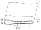
- FIG. 1 is a perspective view schematically showing an example of a battery according to an embodiment
- FIG. 2 is a perspective view schematically showing the configuration of the electrode group in FIG. 1.
- FIG. 3 is a schematic diagram showing the configuration of a current collecting tab of the electrode group of FIG.
- FIG. 4 is a cross-sectional view schematically showing the IV-IV line cross-section of FIG.
- FIG. 5 is a cross-sectional view schematically showing a VV line cross-section of FIG.
- FIG. 6 is a cross-sectional view schematically showing a cross section of an electrode group according to a modification of the embodiment;
- FIG. 1 shows a battery 1 according to an embodiment.
- battery 1 includes electrode group 2 and exterior member 3 .
- the exterior member 3 includes an exterior container 5 and a lid member 6 .
- Each of the outer container 5 and the lid member 6 is made of metal such as aluminum, aluminum alloy, iron, copper, or stainless steel.
- FIG. 1 is a perspective view in which each member is disassembled.
- the outer container 5 has a bottom wall 7 and a peripheral wall 8 .
- An internal cavity 10 in which the electrode group 2 is housed is defined by a bottom wall 7 and a peripheral wall 8 .
- the internal cavity 10 opens toward the side opposite to the side where the bottom wall 7 is located in the height direction.
- the lid member 6 is attached to the peripheral wall 8 at the end opposite the bottom wall 7 . Therefore, the lid member 6 closes the opening of the internal cavity 10 of the outer container 5 , and the lid member 6 and the bottom wall 7 face each other with the internal cavity 10 interposed therebetween in the height direction.
- the electrode group 2 includes a positive electrode 13A and a negative electrode 13B.
- a separator (not shown) is interposed between positive electrode 13A and negative electrode 13B.
- the separator is made of an electrically insulating material and electrically insulates the positive electrode 13A from the negative electrode 13B.
- the positive electrode 13A includes a positive electrode current collector 14A such as a positive electrode current collector foil, and a positive electrode active material-containing layer (not shown) carried on the surface of the positive electrode current collector 14A.
- the positive electrode current collector 14A is, but not limited to, aluminum foil, aluminum alloy foil, or the like.
- the thickness of the positive electrode current collector 14A is about 10 ⁇ m to 20 ⁇ m.
- the positive electrode active material-containing layer includes a positive electrode active material.
- the positive electrode active material-containing layer may optionally contain a binder and a conductive agent.
- Positive electrode active materials include, but are not limited to, oxides, sulfides, and polymers that can intercalate and deintercalate lithium ions.
- the positive electrode current collector 14A includes a positive electrode current collecting tab 15A as a portion where the positive electrode active material-containing layer is not supported.
- the negative electrode 13B includes a negative electrode current collector 14B such as a negative electrode current collector foil, and a negative electrode active material-containing layer (not shown) carried on the surface of the negative electrode current collector 14B.
- the negative electrode current collector 14B is, but not limited to, aluminum foil, aluminum alloy foil, copper foil, or the like.
- the thickness of the negative electrode current collector 14B is about 10 ⁇ m to 20 ⁇ m.
- the negative electrode active material containing layer comprises a negative electrode active material.
- the negative electrode active material layer may optionally contain a binder and a conductive agent.
- the negative electrode active material is, but not limited to, metal oxides, metal sulfides, metal nitrides, carbon materials, and the like that can occlude and release lithium ions.
- the negative electrode current collector 14B includes a negative electrode current collecting tab 15B as a portion on which the negative electrode active material containing layer is not supported.
- the electrode group 2 includes a positive current collecting tab 15A as one of the pair of current collecting tabs 15, and a negative current collecting tab 15B as another one of the pair of current collecting tabs 15 other than the positive current collecting tab 15A.
- the positive electrode 13A, the negative electrode 13B, and the separator are wound around the winding axis with the separator sandwiched between the positive electrode active material-containing layer and the negative electrode active material-containing layer.
- the electrode group 2 has a stack structure in which a plurality of positive electrodes 13A and a plurality of negative electrodes 13B are alternately laminated, and a separator is provided between the positive electrodes 13A and the negative electrodes 13B.
- the positive electrode current collecting tab 15A protrudes with respect to the negative electrode 13B and the separator.
- the negative electrode current collecting tab 15B protrudes from the positive electrode 13A and the separator to the side opposite to the side where the positive electrode current collecting tab 15A projects.
- a pair of current collecting tabs 15 protrude from the internal cavity 10 of the outer container 5 to the side where the peripheral wall 8 is located.
- the electrode group 2 is held (impregnated) with an electrolytic solution (not shown).
- the electrolytic solution may be a non-aqueous electrolytic solution in which an electrolyte is dissolved in an organic solvent, or an aqueous electrolytic solution such as an aqueous solution.
- a gel electrolyte may be used instead of the electrolytic solution, or a solid electrolyte may be used.
- the solid electrolyte intervenes between the positive electrode 13A and the negative electrode 13B instead of the separator in the electrode group. In this case, the positive electrode 13A is electrically insulated from the negative electrode 13B by the solid electrolyte.
- a pair of electrode terminals 16 are attached to the outer surface of the lid member 6 .
- the electrode terminal 16 is made of a conductive material such as metal.
- One of the electrode terminals 16 is the positive terminal (16A) of the battery 1 .
- One of the pair of electrode terminals 16 other than the positive terminal (16A) is the negative terminal (16B) of the battery 1 .
- Each of the electrode terminals 16 is arranged on the outer surface of the lid member 6 . Accordingly, a pair of electrode terminals 16 are installed on the exterior member 3 .
- An insulating member 18 is provided between each of the electrode terminals 16 and the lid member 6 on the outer surface of the lid member 6 .
- Each electrode terminal 16 is electrically insulated from the lid member 6 and the outer container 5 by an insulating member 18 .
- a pair of conductive members 20 are arranged in the internal cavity 10 of the outer container 5 .
- One of the pair of conductive members 20 is a positive electrode conductive member (20A).
- One of the pair of conductive members 20 other than the positive conductive member (20A) is the negative conductive member (20B).
- the positive electrode current collecting tab 15A of the electrode group 2 is electrically connected to the positive electrode terminal 16A through at least the positive electrode conductive member 20A.
- the negative electrode current collecting tab 15B of the electrode group 2 is electrically connected to the negative electrode terminal 16B via at least the negative electrode conductive member 20B.
- Each of the conductive members 20 is formed from a conductive material such as metal.
- a conductive material forming the conductive member 20 is, for example, aluminum, stainless steel, copper, iron, or the like.
- the pair of conductive members 20 are a pair of leads.
- a plurality of band-shaped portions are laminated on each of the current collecting tabs 15 .
- each of the current collecting tabs 15 is bound with a plurality of band-shaped portions. Therefore, each of the current collecting tabs 15 is electrically connected to the corresponding one of the electrode terminals 16 through the corresponding one of the pair of conductive members 20 in a state in which the plurality of band-shaped portions are bound.
- the lid member 6 is formed with a gas release valve 23 and an injection port (not shown).
- a sealing plate 25 is welded to the outer surface of the lid member 6 to close the injection port.
- the gas release valve 23 and the injection port may not be provided in the battery 1 .
- the current collecting tabs (15A and 15B) and the pair of conductive members 20 are electrically insulated from the outer container 5 by one or more insulating members (not shown). be.
- FIG. 2 shows the vicinity of the current collecting tab 15 in the electrode group 2.
- the projecting direction of the current collecting tab 15 (the direction indicated by arrow Y3) and the direction opposite to the projecting direction of the current collecting tab 15 (the direction indicated by arrow Y4) are defined.
- the width direction (direction indicated by arrows Z3 and Z4) intersecting (perpendicular or substantially orthogonal) to the projecting direction of the current collecting tab 15 and the projecting direction and width direction of the current collecting tab 15
- a thickness direction (direction indicated by arrow X3 and arrow X4) is defined that intersects both.
- the dimension in the thickness direction is smaller than the dimension in the projecting direction and the dimension in the width direction of the current collecting tab 15 .
- the width direction of the electrode group 2 matches or substantially matches the height direction of the battery 1, and the thickness direction matches or substantially matches the depth direction of the battery 1. It is placed in a state where Further, as shown in FIG. 2 and the like, the current collecting tab 15 is formed with a first concave portion 31 and a second concave portion 32 . 3 to 5 show first recesses 31 and second recesses 32 formed in a plurality of band-shaped portions of the current collecting tab 15.
- FIG. 3 to 5, in the electrode group 2, the projecting direction of the current collecting tab 15, the direction opposite to the projecting direction of the current collecting tab 15, the width direction, and the thickness direction are defined in the same manner as in FIG.
- FIG. 4 is a sectional view taken along the line IV-IV in FIG. 3 and showing a cross section orthogonal or substantially orthogonal to the width direction of the electrode group 2.
- FIG. 5 is a cross-sectional view showing a cross section taken along the line VV in FIG. 3, which is perpendicular or substantially perpendicular to the projecting direction of the current collecting tab 15. As shown in FIG.
- the current collecting tab 15 is formed with a first recess 31 and a second recess 32 adjacent to the first recess 31 from the outer peripheral side.
- each of the first recess 31 and the second recess 32 is formed by ultrasonic bonding or the like.
- the first recess 31 has an edge E1.
- the second recess 32 has an edge E2.
- the outer edge of the first recess 31 is defined by the edge E1.
- the outer edge of the second recess 32 is defined by the edge E2.
- the edge E2 is arranged on the outer peripheral side of the edge E1 without being connected to the edge E1. Therefore, the second recess 32 is formed between the edge E1 and the edge E2.
- the first recess 31 is formed in a rectangular shape or a substantially rectangular shape when viewed from one side in the thickness direction of the electrode group 2 .
- the shape of the first concave portion 31 viewed from one side in the thickness direction of the electrode group 2 is not limited to this, and can be appropriately set according to the shape of the current collecting tab 15 or the like.
- a plurality of first recesses 31 are formed in the current collecting tab 15 .
- the multiple first recesses 31 are close to each other.
- all of the plurality of first recesses 31 are formed together.
- all of the plurality of first recesses 31 form a first recess group.
- the second recess is formed adjacent to the outer peripheral side of the plurality of first recesses (first recess group).
- adjacent first recesses 31 are not connected to each other. That is, the edges E1 of adjacent first recesses 31 are not connected to each other.
- an intermediate portion 33 is formed between adjacent first recesses 31 .
- the intermediate portion 33 extends between the edges E1 of the adjacent first recesses 31 .
- it is assumed that the shapes of the plurality of first recesses 31 are the same or substantially the same.
- the plurality of first recesses 31 are formed side by side in the projecting direction of the current collecting tab 15, and the plurality of first recesses 31 are formed side by side in the width direction. 2 and 3, the two first recesses 31 are formed side by side in the projecting direction of the current collection tab 15, and the four first recesses 31 are formed side by side in the width direction. It is formed. That is, eight first recesses 31 are formed in the current collecting tab 15 of this example. In this way, when the plurality of first recesses 31 are formed side by side in both the projecting direction and the width direction of the current collecting tab 15, some of the plurality of first recesses 31 are adjacent to each other in the projecting direction of the current collecting tab 15 .
- the intermediate portion 33 described above includes a portion 33A (first intermediate portion 33A) extending along the projecting direction of the current collecting tab 15 and a portion 33B (second intermediate portion 33A) extending along the width direction. and an intermediate portion 33B).
- the intermediate portion 33 includes a plurality of first intermediate portions 33A and a plurality of second intermediate portions 33B.
- a plurality of first intermediate portions 33A and a plurality of second intermediate portions 33B are formed in a mutually connected state.
- first recesses 31 there may be first recesses 31 that are not arranged adjacent to the second recesses 32 depending on the arrangement of the plurality of first recesses 31 .
- the second recesses 32 are adjacent to at least some first recesses 31 of the plurality of first recesses 31 from the outer peripheral side of the entire plurality of first recesses 31 .
- the current collecting tab 15 has a connection portion CP connected to the conductive member 20. As shown in FIGS. At the connection portion CP, the current collecting tab 15 is formed with a first surface S ⁇ b>1 that joins with the conductive member 20 . In addition, in the connecting portion CP, the current collecting tab 15 is formed with a second surface S2 on the side opposite to the first surface S1 with respect to the stacking direction of the current collecting tab 15 (the thickness direction of the electrode group 2). In the connection portion CP, the plurality of band-shaped portions of the current collecting tab 15 are laminated between the first surface S1 and the second surface S2 in the stacking direction of the current collecting tab 15 . 4 and 5, the plurality of band-shaped portions stacked on the current collecting tab 15 are integrated by, for example, ultrasonic bonding. Therefore, the second surface S2 is deformed along the shapes of the first concave portion 31 and the second concave portion 32 .
- FIG. 4 shows two cross sections of the first recess 31 and the second recess 32 with respect to the projecting direction of the current collecting tab 15 .
- FIG. 5 also shows cross sections of the four first recesses 31 and four second recesses 32 in the width direction of the electrode group 2 .
- the first recessed portion 31 and the second recessed portion 32 are recessed toward the conductive member 20 in the stacking direction of the current collecting tabs 15 .
- the recesses of the first recess 31 and the second recess 32 toward the conductive member 20 are formed by ultrasonic bonding. By recessing the first recess 31 and the second recess 32 in this manner, the current collecting tab 15 and the conductive member 20 are connected.
- recesses are formed in the conductive member 20 corresponding to the recesses of the first recess 31 and the second recess 32 .
- the maximum recess amount of the second recess 32 is smaller than the maximum recess amount of the first recess.
- the recess amount is the distance from the corresponding edge portion of the position recessed on the side where the conductive member 20 is located in the stacking direction of the current collecting tabs 15 .
- the maximum amount of recession of the first recess 31 is the distance between the edge E1 and the position where the first recess 31 is most recessed in the stacking direction of the current collecting tabs 15 .
- the maximum amount of recession of the second recess 32 is the distance between the edge E2 and the position where the second recess 32 is most recessed in the stacking direction of the current collecting tabs.
- the first recess 31 has two edges E1 that are offset from each other in the stacking direction of the current collecting tabs 15 .
- the maximum amount of recession of the first recess 31 is defined as the distance from the edge E1 at the farthest position from the position where the first recess 31 is most recessed in the stacking direction of the current collecting tabs 15 .
- the amount of recession of the second recess 32 is the distance between the edge E2 and the position where the second recess 32 is most recessed in the stacking direction of the current collecting tabs 15 . Therefore, as shown in FIG. 4, the recess amount of the first recess 31 is d1, and the recess amount of the second recess 32 is d2. As mentioned above, d2 is less than d1 (d2 ⁇ d1).
- the first recess 31 is recessed over the conductive member 20 . That is, the position where the first recess 31 has the largest recess amount (the deepest position of the first recess 31) is located on the side where the conductive member 20 is located with respect to the first surface S1 in the thickness direction.
- the position of the first recess 31 where the amount of recession is the largest corresponds to the position of the first recess 31 that is the farthest from the edge E1 in the stacking direction of the current collecting tabs 15 .
- the first recess 31 has a first inclined wall 31S.
- the first inclined wall 31S is formed over the entire circumference of the first recess.
- the first inclined wall 31S is formed so that the recess amount decreases toward the outer peripheral side of the first recess 31 (the side where the edge E1 corresponding to the first recess 31 is located).
- the second recess 32 also has a second inclined wall 32S.
- the second inclined wall 32S is formed over the entire circumference of the second recess.
- the second inclined wall 32S is formed so that the recess amount decreases toward the outer peripheral side of the second recess 32 (the side where the edge E2 corresponding to the second recess 32 is located).
- first inclined wall 31S and the second inclined wall 32S are formed in this way, the first inclined wall 31S and the second inclined wall 32S are inclined with respect to the joint surface with the first surface S1. do. That is, the first inclined wall 31S and the second inclined wall 32S are inclined with respect to the first surface S1.
- the amount of inclination of the second inclined wall 32S is smaller than the amount of inclination of the first inclined wall 31S.
- the amount of inclination represents the degree of inclination of the inclined wall (the first inclined wall 31S or the second inclined wall 32S) with respect to the joint surface with the first surface S1.
- the amount of inclination is the degree of inclination of the inclined wall with respect to the first surface S1.
- the amount of inclination of the first inclined wall 31S is represented by the angle ⁇ 1.
- the amount of inclination of the second inclined wall 32S is represented by the angle ⁇ 2.
- ⁇ 2 is smaller than ⁇ 1 ( ⁇ 2 ⁇ 1).
- the first inclined wall 31S of the first recess 31 is formed in a state in which the recess amount decreases toward the outer peripheral side of the first recess 31.
- the second inclined wall 32 ⁇ /b>S of the second recessed portion 32 is formed in a state in which the amount of recession decreases toward the outer peripheral side of the second recessed portion 32 .
- the first slanted wall 31S and the second slanted wall 32S are slanted with respect to the conductive member 20, that is, the first surface S1.
- the depression amounts d1 and d2 and the inclination amounts ⁇ 1 and ⁇ 2 are defined in the same manner as in FIG. In the cross section shown in FIG.
- the angle formed by the first inclined walls 31S in a certain first concave portion 31 is preferably 90° or less.
- the angles formed by the first inclined walls 31S in all of the plurality of first recesses 31 be 90° or less.
- the plurality of first recesses 31 are formed in the current collecting tab 15 in close proximity to each other. Therefore, as shown in FIGS. 4 and 5, between the first concave portions 31 adjacent to each other, there is a convex portion 34 projecting toward the opposite side of the conductive member 20 in the stacking direction of the current collecting tabs 15 . It is formed.
- the protrusions 34 are formed between the first inclined walls 31S of the adjacent first recesses 31 in both the projecting direction and the width direction of the current collecting tab 15 . In the state shown in FIG. 3, the projecting end of the convex portion 34 forms the intermediate portion 33 (the first intermediate portion 33A or the second intermediate portion 33B).
- the protruding end of the convex portion 34 is positioned closer to the conductive member 20 than the position where the second concave portion 32 is recessed the most.
- the position of the second recess 32 where the amount of recession is the largest corresponds to the position of the second recess 32 that is the farthest from the edge E2 in the stacking direction of the current collecting tabs 15 .
- all of the protruding ends of the plurality of protrusions 34 are located at the deepest position (the position where the amount of recession is the largest) of the second recess 32 . ) on the side where the conductive member 20 is located.
- the first concave portion 31 and the second concave portion 32 are formed at the connecting portion between the current collecting tab (corresponding one of 15A and 15B) and the conductive member 20 . Therefore, in the manufacturing method of the battery 1 , the first concave portion 31 and the second concave portion 32 are formed when the conductive member 20 and the current collecting tab 15 are connected.
- electrode terminals 16 16 A, 16 B
- the active material-containing layer is supported on the current collector (one of 14A and 14B) of the electrode group 2, and the active material-containing layer is not supported on the current collector (one of 14A and 14B).
- a current collecting tab 15 is formed.
- a first recess 31 recessed toward the conductive member 20 is formed at the connection portion CP between the current collecting tab 15 and the conductive member 20 . Also, a second recess 32 recessed toward the conductive member 20 with a recess amount smaller than that of the first recess 31 is formed at a position adjacent to the outer peripheral side of the first recess 31 . Thereby, the conductive member 20 and the current collecting tab 15 are electrically connected.
- a first concave portion 31 and a second concave portion 32 are formed in the current collecting tab 15 provided on the current collector of the electrode group 2 (corresponding one of 14A and 14B).
- the first recessed portion 31 is formed in the connecting portion of the current collecting tab 15 with the conductive member 20 and is recessed toward the conductive member 20 .
- the second recessed portion 32 is adjacent to the outer periphery of the first recessed portion 31 and is recessed toward the conductive member 20 , and has a smaller maximum recessed amount than the first recessed portion 31 .
- Such first recess 31 and second recess 32 are formed by, for example, ultrasonic bonding.
- concentration of stress on the current collecting foil or the like forming the current collecting tab 15 is alleviated. That is, since the amount of deformation of the current collector foil or the like is reduced, tearing of the current collector foil or the like is effectively suppressed.
- the current collecting foil or the like is pressed by the second concave portion 32 over a wider range than only the first concave portion 31, the current collecting tab 15 is prevented from being wrinkled.
- the first recess 31 has a first inclined wall 31S
- the second recess 32 has a second inclined wall 32S.
- the first inclined wall 31 ⁇ /b>S has a smaller concave amount toward the outer peripheral side of the first concave portion 31 .
- the second inclined wall 32 ⁇ /b>S has a smaller concave amount toward the outer peripheral side of the second recessed portion 32 .
- the amount of inclination of the second inclined wall 32S is smaller than the amount of inclination of the first inclined wall 31S.
- the plurality of first recesses 31 are formed in close proximity to each other.
- a second recess is formed on the outer peripheral side of the plurality of first recesses.
- the first recess 31 is recessed over the conductive member 20 in the thickness direction. Thereby, the current collecting tab 15 and the conductive member 20 are more sufficiently joined.
- the first recess 31 may not be formed in the conductive member 20 . That is, the first concave portion 31 is formed only in the current collecting tab 15 in the connection portion CP.
- the position of the first recess 31 where the amount of recession is the largest is located on the side where the current collecting tab 15 is located with respect to the first surface S1 in the thickness direction.
- the second recessed portion 32 is adjacent to the outer peripheral side of the first recessed portion 31 and is recessed toward the conductive member 20 , and the maximum recessed amount is smaller than that of the first recessed portion 31 . Therefore, also in this modified example, the same functions and effects as those of the above-described embodiment and the like can be obtained.
- the electrode group 2 in the internal cavity 10 of the battery 1 , has a width direction that matches or substantially matches the lateral direction of the battery 1 and a thickness direction that matches or substantially matches the depth direction of the battery 1 . state, may be placed.
- the projecting direction of the current collecting tab 15 coincides or substantially coincides with the direction in which the lid member 6 is positioned in the height direction of the battery 1 .
- Reference Document 1 Japanese Patent Application Laid-Open No. 2012-209260
- the positive electrode current collecting tab 15A and the negative electrode current collecting tab 15B protrude to the same side relative to each other.
- the exterior member of the battery 1 is not limited to the structure formed from the exterior container 5 and the lid member 6 .
- the exterior portion may be formed from first and second metal exterior members, as in Reference Document 2 (International Publication No. 2016/204147).
- the first exterior member has a bottom wall and a peripheral wall, and in the first exterior member, the flange protrudes outward from the end of the peripheral wall opposite to the bottom wall.
- a second exterior member is attached to the flange of the first exterior member.
- the exterior of the battery may be formed from a laminate film having a three-layer structure in which a metal layer is sandwiched between resin layers.
- the first concave portion 31 and the second concave portion 32 are formed in the current collecting tab 15 in the same manner as in any of the above-described embodiments.
- the shapes of the plurality of first recesses 31 are not formed identically or substantially identically.
- the second recesses 32 may be formed such that the maximum recession amount is smaller than the maximum recession amount defined for each of the plurality of first recesses 31 .
- the maximum recession amount which is the largest of the maximum recession amounts defined for each of the plurality of first recesses 31 , should be larger than the maximum recession amount for the second recesses 32 .
- the first recess is formed in the connection portion of the current collecting tab with the conductive member and is recessed toward the conductive member.
- the second recess is adjacent to the outer periphery of the first recess and is recessed toward the conductive member, and has a smaller maximum recess than the first recess. This makes it possible to provide a battery capable of suppressing a decrease in strength due to bonding of the current collecting tabs.
Abstract
Description
図1は、実施形態に係る電池1を示す。図1に示すように、電池1は、電極群2及び外装部材3を備える。外装部材3は、外装容器5及び蓋部材6を備える。外装容器5及び蓋部材6のそれぞれは、アルミニウム、アルミニウム合金、鉄、銅又はステンレス等の金属から形成される。ここで、電池1(外装容器5)では、奥行き方向(矢印X1及び矢印X2で示す方向)、奥行き方向に対して交差する(直交又は略直交な)横方向(矢印Y1及び矢印Y2で示す方向)、及び、奥行き方向及び横方向の両方に対して交差する(直交又は略直交な)高さ方向(矢印Z1及び矢印Z2で示す方向)が、規定される。電池1及び外装容器5のそれぞれでは、奥行き方向についての寸法が、横方向についての寸法、及び、高さ方向についての寸法のそれぞれに比べて、小さい。なお、図1は、部材ごとに分解して示す斜視図である。 (embodiment)
FIG. 1 shows a
図6に示すように、ある変形例では、第1の凹部31が導電部材20に形成されていなくてもよい。すなわち、第1の凹部31は、接続部分CPにおいて、集電タブ15のみに形成されている。本変形例では、第1の凹部31の最も凹み量が大きい位置は、厚さ方向について、第1の面S1に対して集電タブ15が位置する側に位置する。本変形例においても、第2の凹部32は、第1の凹部31の外周側に隣接するとともに導電部材20に向かって凹み、第1の凹部31より最大凹み量が小さい。そのため、本変形例においても、前述の実施形態等と同様の作用及び効果を奏する。 (Modification)
As shown in FIG. 6 , in some variations, the
Claims (11)
- 外装部材と、
前記外装部材に設置される電極端子と、
前記外装部材の内部空洞に収納される電極群であって、集電体及び前記集電体に担持される活物質含有層を備え、前記集電体は前記活物質含有層が未担持である集電タブを備える電極群と、
前記電極端子と前記集電タブとの間を電気的に接続する導電部材と、
前記集電タブにおいて前記導電部材との接続部分に形成され、前記導電部材に向かって凹む第1の凹部と、
前記第1の凹部の外周側に形成されるとともに、前記導電部材に向かって凹む第2の凹部であって、前記第1の凹部より最大凹み量が小さい第2の凹部と、
を具備する、電池。 an exterior member;
an electrode terminal installed on the exterior member;
A group of electrodes housed in an internal cavity of the exterior member, comprising a current collector and an active material-containing layer supported on the current collector, wherein the current collector does not support the active material-containing layer. an electrode group comprising a current collecting tab;
a conductive member electrically connecting between the electrode terminal and the current collecting tab;
a first recess formed in the current collecting tab at a portion connected to the conductive member and recessed toward the conductive member;
a second recess formed on the outer peripheral side of the first recess and recessed toward the conductive member, the second recess having a smaller maximum recess amount than the first recess;
A battery comprising: - 前記集電タブは、前記導電部材との前記接続部分において前記導電部材と接合する第1の面と、前記接続部分において前記第1の面とは反対側に形成される第2の面と、を備え、
前記第2の面に、前記第1の凹部及び前記第2の凹部が形成される、
請求項1に記載の電池。 The current collecting tab has a first surface that is joined to the conductive member at the connection portion with the conductive member, a second surface that is formed at the connection portion on the side opposite to the first surface, with
the first recess and the second recess are formed on the second surface;
A battery according to claim 1 . - 前記第1の凹部は、前記第1の凹部31の外周側に向かうにつれて凹み量が小さい第1の傾斜壁を備え、
前記第2の凹部は、前記第2の凹部32の外周側に向かうにつれて凹み量が小さい第2の傾斜壁であって、前記導電部材に対する傾斜量が前記第1の傾斜壁より小さい第2の傾斜壁を備える、
請求項1又は2に記載の電池。 The first recess has a first inclined wall whose recess amount decreases toward the outer peripheral side of the first recess 31,
The second concave portion is a second inclined wall whose concave amount decreases toward the outer circumference of the second concave portion 32, and the inclination amount with respect to the conductive member is smaller than that of the first inclined wall. with sloping walls,
The battery according to claim 1 or 2. - 複数の前記第1の凹部が、互いに対して近接した状態で前記接続部分に形成され、
前記第2の凹部が、複数の前記第1の凹部の外周側に形成される、
請求項1~3のいずれか1項に記載の電池。 a plurality of the first recesses formed in the connecting portion in close proximity to each other;
The second recess is formed on the outer peripheral side of the plurality of first recesses,
The battery according to any one of claims 1-3. - 隣接する複数の前記第1の凹部が、前記導電部材とは反対側に向かって突出する凸部を形成する、
請求項4に記載の電池。 A plurality of adjacent first recesses form a protrusion that protrudes toward the side opposite to the conductive member,
The battery according to claim 4. - 前記凸部の突出端は、前記第2の凹部の最も凹み量が大きい位置と比べて、導電部材に近い側に位置する、
請求項5に記載の電池。 The protruding end of the protrusion is located closer to the conductive member than the position of the second recess where the amount of recession is the largest,
The battery according to claim 5. - 前記第1の凹部は、前記導電部材とは反対側から視て、長方形状に形成される、
請求項1~6のいずれか1項に記載の電池。 The first recess is formed in a rectangular shape when viewed from the side opposite to the conductive member,
The battery according to any one of claims 1-6. - 前記第1の凹部及び前記第2の凹部は、超音波接合により形成される、
請求項1~7のいずれか1項に記載の電池。 The first recess and the second recess are formed by ultrasonic bonding,
The battery according to any one of claims 1-7. - 前記第1の凹部は、前記導電部材にまでわたって凹む、
請求項1~8のいずれか1項に記載の電池。 The first recess is recessed over the conductive member,
The battery according to any one of claims 1-8. - 外装部材に電極端子を設置することと、
前記外装部材の内部空洞に電極群を収納することと、
前記電極群の集電体に活物質含有層を担持することと、
前記活物質含有層が前記集電体に担持されない部位として集電タブを形成することと、
前記電極端子と前記集電タブとの間を導電部材により電気的に接続することと、
前記集電タブと前記導電部材との接続部分において、前記導電部材に向かって凹む第1の凹部を形成することと、
前記第1の凹部の外周側において、前記第1の凹部より凹み量が小さい状態で前記導電部材に向かって凹む第2の凹部を形成することと、
を具備する、製造方法。 installing an electrode terminal on the exterior member;
housing an electrode group in an internal cavity of the exterior member;
supporting an active material-containing layer on the current collector of the electrode group;
forming a current collecting tab as a portion where the active material-containing layer is not supported by the current collector;
electrically connecting the electrode terminal and the current collecting tab with a conductive member;
forming a first recess recessed toward the conductive member at a connecting portion between the current collecting tab and the conductive member;
forming a second recess that is recessed toward the conductive member in a state that the amount of recess is smaller than that of the first recess, on the outer peripheral side of the first recess;
A manufacturing method comprising: - 前記第1の凹部を形成することは、超音波接合により前記導電部材に向かって前記第1の凹部を凹ませることを備え、
前記第2の凹部を形成することは、超音波接合により前記導電部材に向かって前記第2の凹部を凹ませることを備える、
請求項10に記載の製造方法。 forming the first recess comprises recessing the first recess toward the conductive member by ultrasonic bonding;
forming the second recess comprises recessing the second recess toward the conductive member by ultrasonic bonding;
The manufacturing method according to claim 10.
Priority Applications (6)
| Application Number | Priority Date | Filing Date | Title |
|---|---|---|---|
| CN202180016956.9A CN115244779A (en) | 2021-02-25 | 2021-02-25 | Battery and method for manufacturing battery |
| EP21927839.7A EP4300700A1 (en) | 2021-02-25 | 2021-02-25 | Battery and method for manufacturing battery |
| KR1020227028902A KR20220129619A (en) | 2021-02-25 | 2021-02-25 | Batteries and battery manufacturing methods |
| JP2022538843A JP7379713B2 (en) | 2021-02-25 | 2021-02-25 | Batteries and battery manufacturing methods |
| PCT/JP2021/007059 WO2022180737A1 (en) | 2021-02-25 | 2021-02-25 | Battery and method for manufacturing battery |
| US17/933,384 US20230011735A1 (en) | 2021-02-25 | 2022-09-19 | Battery and manufacturing method of battery |
Applications Claiming Priority (1)
| Application Number | Priority Date | Filing Date | Title |
|---|---|---|---|
| PCT/JP2021/007059 WO2022180737A1 (en) | 2021-02-25 | 2021-02-25 | Battery and method for manufacturing battery |
Related Child Applications (1)
| Application Number | Title | Priority Date | Filing Date |
|---|---|---|---|
| US17/933,384 Continuation US20230011735A1 (en) | 2021-02-25 | 2022-09-19 | Battery and manufacturing method of battery |
Publications (1)
| Publication Number | Publication Date |
|---|---|
| WO2022180737A1 true WO2022180737A1 (en) | 2022-09-01 |
Family
ID=83047893
Family Applications (1)
| Application Number | Title | Priority Date | Filing Date |
|---|---|---|---|
| PCT/JP2021/007059 WO2022180737A1 (en) | 2021-02-25 | 2021-02-25 | Battery and method for manufacturing battery |
Country Status (6)
| Country | Link |
|---|---|
| US (1) | US20230011735A1 (en) |
| EP (1) | EP4300700A1 (en) |
| JP (1) | JP7379713B2 (en) |
| KR (1) | KR20220129619A (en) |
| CN (1) | CN115244779A (en) |
| WO (1) | WO2022180737A1 (en) |
Citations (8)
| Publication number | Priority date | Publication date | Assignee | Title |
|---|---|---|---|---|
| JP2004055511A (en) * | 2002-05-31 | 2004-02-19 | Sanyo Electric Co Ltd | Battery |
| JP2010282846A (en) | 2009-06-04 | 2010-12-16 | Toyota Motor Corp | Secondary battery and method of manufacturing the same |
| JP2012209260A (en) | 2012-06-18 | 2012-10-25 | Toshiba Corp | Battery |
| JP2014022153A (en) * | 2012-07-17 | 2014-02-03 | Toyota Industries Corp | Electricity storage device |
| JP2014212012A (en) * | 2013-04-18 | 2014-11-13 | トヨタ自動車株式会社 | Method of manufacturing secondary battery and secondary battery |
| WO2016204147A1 (en) | 2015-06-15 | 2016-12-22 | 株式会社 東芝 | Battery and battery pack |
| WO2018159197A1 (en) * | 2017-02-28 | 2018-09-07 | 日立オートモティブシステムズ株式会社 | Secondary battery |
| JP2019139954A (en) * | 2018-02-09 | 2019-08-22 | トヨタ自動車株式会社 | Method for manufacturing power storage device |
Family Cites Families (2)
| Publication number | Priority date | Publication date | Assignee | Title |
|---|---|---|---|---|
| US20100003599A1 (en) * | 2006-11-15 | 2010-01-07 | Takashi Nonoshita | Method for producing current collector for non-aqueous electrolyte secondary battery, method for producing electrode for non-aqueous electrolyte secondary battery, and non-aqueous electrolyte secondary battery |
| JP2014010913A (en) * | 2012-06-27 | 2014-01-20 | Toyota Motor Corp | Secondary battery and manufacturing method thereof |
-
2021
- 2021-02-25 WO PCT/JP2021/007059 patent/WO2022180737A1/en active Application Filing
- 2021-02-25 JP JP2022538843A patent/JP7379713B2/en active Active
- 2021-02-25 EP EP21927839.7A patent/EP4300700A1/en active Pending
- 2021-02-25 CN CN202180016956.9A patent/CN115244779A/en active Pending
- 2021-02-25 KR KR1020227028902A patent/KR20220129619A/en unknown
-
2022
- 2022-09-19 US US17/933,384 patent/US20230011735A1/en active Pending
Patent Citations (8)
| Publication number | Priority date | Publication date | Assignee | Title |
|---|---|---|---|---|
| JP2004055511A (en) * | 2002-05-31 | 2004-02-19 | Sanyo Electric Co Ltd | Battery |
| JP2010282846A (en) | 2009-06-04 | 2010-12-16 | Toyota Motor Corp | Secondary battery and method of manufacturing the same |
| JP2012209260A (en) | 2012-06-18 | 2012-10-25 | Toshiba Corp | Battery |
| JP2014022153A (en) * | 2012-07-17 | 2014-02-03 | Toyota Industries Corp | Electricity storage device |
| JP2014212012A (en) * | 2013-04-18 | 2014-11-13 | トヨタ自動車株式会社 | Method of manufacturing secondary battery and secondary battery |
| WO2016204147A1 (en) | 2015-06-15 | 2016-12-22 | 株式会社 東芝 | Battery and battery pack |
| WO2018159197A1 (en) * | 2017-02-28 | 2018-09-07 | 日立オートモティブシステムズ株式会社 | Secondary battery |
| JP2019139954A (en) * | 2018-02-09 | 2019-08-22 | トヨタ自動車株式会社 | Method for manufacturing power storage device |
Also Published As
| Publication number | Publication date |
|---|---|
| US20230011735A1 (en) | 2023-01-12 |
| KR20220129619A (en) | 2022-09-23 |
| EP4300700A1 (en) | 2024-01-03 |
| JP7379713B2 (en) | 2023-11-14 |
| CN115244779A (en) | 2022-10-25 |
| JPWO2022180737A1 (en) | 2022-09-01 |
Similar Documents
| Publication | Publication Date | Title |
|---|---|---|
| JP7367741B2 (en) | Energy storage element | |
| JP5564278B2 (en) | Secondary battery | |
| JP2010212241A (en) | Secondary battery | |
| JP6550848B2 (en) | Prismatic secondary battery | |
| JP5225805B2 (en) | Secondary battery and manufacturing method thereof | |
| EP2610945A1 (en) | Stacked cell | |
| US20220271399A1 (en) | Battery | |
| US10424809B2 (en) | Secondary battery, method for manufacturing same, and battery pack employing same | |
| JP2020524366A (en) | Stacked prismatic structure for electrochemical cells | |
| EP3086382B1 (en) | Rechargeable battery | |
| JP2016162755A (en) | Rechargeable battery having cover | |
| JP2022050804A (en) | Secondary battery | |
| EP2650943A1 (en) | Rechargeable battery | |
| JP6232213B2 (en) | Secondary battery and manufacturing method thereof | |
| JP4451654B2 (en) | Lithium secondary battery | |
| CN106328843B (en) | Secondary battery | |
| WO2022180737A1 (en) | Battery and method for manufacturing battery | |
| JP6715936B2 (en) | Prismatic secondary battery | |
| WO2023037407A1 (en) | Battery | |
| JP6561866B2 (en) | Stacked battery | |
| WO2021181563A1 (en) | Connection lead and battery | |
| WO2023032151A1 (en) | Battery | |
| US20220271400A1 (en) | Battery | |
| US20230223657A1 (en) | Battery | |
| WO2023170943A1 (en) | Battery, and method for manufacturing battery |
Legal Events
| Date | Code | Title | Description |
|---|---|---|---|
| ENP | Entry into the national phase |
Ref document number: 2022538843 Country of ref document: JP Kind code of ref document: A |
|
| 121 | Ep: the epo has been informed by wipo that ep was designated in this application |
Ref document number: 21927839 Country of ref document: EP Kind code of ref document: A1 |
|
| WWE | Wipo information: entry into national phase |
Ref document number: 2021927839 Country of ref document: EP |
|
| NENP | Non-entry into the national phase |
Ref country code: DE |
|
| ENP | Entry into the national phase |
Ref document number: 2021927839 Country of ref document: EP Effective date: 20230925 |