WO2022175784A1 - 表示装置 - Google Patents
表示装置 Download PDFInfo
- Publication number
- WO2022175784A1 WO2022175784A1 PCT/IB2022/051140 IB2022051140W WO2022175784A1 WO 2022175784 A1 WO2022175784 A1 WO 2022175784A1 IB 2022051140 W IB2022051140 W IB 2022051140W WO 2022175784 A1 WO2022175784 A1 WO 2022175784A1
- Authority
- WO
- WIPO (PCT)
- Prior art keywords
- layer
- light
- lower electrode
- electrode
- region
- Prior art date
- Legal status (The legal status is an assumption and is not a legal conclusion. Google has not performed a legal analysis and makes no representation as to the accuracy of the status listed.)
- Ceased
Links
Images


Classifications
-
- H—ELECTRICITY
- H10—SEMICONDUCTOR DEVICES; ELECTRIC SOLID-STATE DEVICES NOT OTHERWISE PROVIDED FOR
- H10K—ORGANIC ELECTRIC SOLID-STATE DEVICES
- H10K59/00—Integrated devices, or assemblies of multiple devices, comprising at least one organic light-emitting element covered by group H10K50/00
- H10K59/10—OLED displays
- H10K59/12—Active-matrix OLED [AMOLED] displays
- H10K59/121—Active-matrix OLED [AMOLED] displays characterised by the geometry or disposition of pixel elements
-
- H—ELECTRICITY
- H10—SEMICONDUCTOR DEVICES; ELECTRIC SOLID-STATE DEVICES NOT OTHERWISE PROVIDED FOR
- H10K—ORGANIC ELECTRIC SOLID-STATE DEVICES
- H10K71/00—Manufacture or treatment specially adapted for the organic devices covered by this subclass
- H10K71/10—Deposition of organic active material
- H10K71/12—Deposition of organic active material using liquid deposition, e.g. spin coating
- H10K71/13—Deposition of organic active material using liquid deposition, e.g. spin coating using printing techniques, e.g. ink-jet printing or screen printing
- H10K71/135—Deposition of organic active material using liquid deposition, e.g. spin coating using printing techniques, e.g. ink-jet printing or screen printing using ink-jet printing
-
- G—PHYSICS
- G09—EDUCATION; CRYPTOGRAPHY; DISPLAY; ADVERTISING; SEALS
- G09F—DISPLAYING; ADVERTISING; SIGNS; LABELS OR NAME-PLATES; SEALS
- G09F9/00—Indicating arrangements for variable information in which the information is built-up on a support by selection or combination of individual elements
- G09F9/30—Indicating arrangements for variable information in which the information is built-up on a support by selection or combination of individual elements in which the desired character or characters are formed by combining individual elements
-
- H—ELECTRICITY
- H05—ELECTRIC TECHNIQUES NOT OTHERWISE PROVIDED FOR
- H05B—ELECTRIC HEATING; ELECTRIC LIGHT SOURCES NOT OTHERWISE PROVIDED FOR; CIRCUIT ARRANGEMENTS FOR ELECTRIC LIGHT SOURCES, IN GENERAL
- H05B33/00—Electroluminescent light sources
- H05B33/02—Details
- H05B33/06—Electrode terminals
-
- H—ELECTRICITY
- H05—ELECTRIC TECHNIQUES NOT OTHERWISE PROVIDED FOR
- H05B—ELECTRIC HEATING; ELECTRIC LIGHT SOURCES NOT OTHERWISE PROVIDED FOR; CIRCUIT ARRANGEMENTS FOR ELECTRIC LIGHT SOURCES, IN GENERAL
- H05B33/00—Electroluminescent light sources
- H05B33/12—Light sources with substantially two-dimensional [2D] radiating surfaces
- H05B33/14—Light sources with substantially two-dimensional [2D] radiating surfaces characterised by the chemical or physical composition or the arrangement of the electroluminescent material, or by the simultaneous addition of the electroluminescent material in or onto the light source
-
- H—ELECTRICITY
- H05—ELECTRIC TECHNIQUES NOT OTHERWISE PROVIDED FOR
- H05B—ELECTRIC HEATING; ELECTRIC LIGHT SOURCES NOT OTHERWISE PROVIDED FOR; CIRCUIT ARRANGEMENTS FOR ELECTRIC LIGHT SOURCES, IN GENERAL
- H05B33/00—Electroluminescent light sources
- H05B33/12—Light sources with substantially two-dimensional [2D] radiating surfaces
- H05B33/22—Light sources with substantially two-dimensional [2D] radiating surfaces characterised by the chemical or physical composition or the arrangement of auxiliary dielectric or reflective layers
-
- H—ELECTRICITY
- H05—ELECTRIC TECHNIQUES NOT OTHERWISE PROVIDED FOR
- H05B—ELECTRIC HEATING; ELECTRIC LIGHT SOURCES NOT OTHERWISE PROVIDED FOR; CIRCUIT ARRANGEMENTS FOR ELECTRIC LIGHT SOURCES, IN GENERAL
- H05B33/00—Electroluminescent light sources
- H05B33/12—Light sources with substantially two-dimensional [2D] radiating surfaces
- H05B33/26—Light sources with substantially two-dimensional [2D] radiating surfaces characterised by the composition or arrangement of the conductive material used as an electrode
- H05B33/28—Light sources with substantially two-dimensional [2D] radiating surfaces characterised by the composition or arrangement of the conductive material used as an electrode of translucent electrodes
-
- H—ELECTRICITY
- H10—SEMICONDUCTOR DEVICES; ELECTRIC SOLID-STATE DEVICES NOT OTHERWISE PROVIDED FOR
- H10K—ORGANIC ELECTRIC SOLID-STATE DEVICES
- H10K50/00—Organic light-emitting devices
- H10K50/10—OLEDs or polymer light-emitting diodes [PLED]
- H10K50/14—Carrier transporting layers
- H10K50/15—Hole transporting layers
-
- H—ELECTRICITY
- H10—SEMICONDUCTOR DEVICES; ELECTRIC SOLID-STATE DEVICES NOT OTHERWISE PROVIDED FOR
- H10K—ORGANIC ELECTRIC SOLID-STATE DEVICES
- H10K50/00—Organic light-emitting devices
- H10K50/10—OLEDs or polymer light-emitting diodes [PLED]
- H10K50/17—Carrier injection layers
-
- H—ELECTRICITY
- H10—SEMICONDUCTOR DEVICES; ELECTRIC SOLID-STATE DEVICES NOT OTHERWISE PROVIDED FOR
- H10K—ORGANIC ELECTRIC SOLID-STATE DEVICES
- H10K59/00—Integrated devices, or assemblies of multiple devices, comprising at least one organic light-emitting element covered by group H10K50/00
- H10K59/10—OLED displays
- H10K59/12—Active-matrix OLED [AMOLED] displays
- H10K59/1201—Manufacture or treatment
-
- H—ELECTRICITY
- H10—SEMICONDUCTOR DEVICES; ELECTRIC SOLID-STATE DEVICES NOT OTHERWISE PROVIDED FOR
- H10K—ORGANIC ELECTRIC SOLID-STATE DEVICES
- H10K59/00—Integrated devices, or assemblies of multiple devices, comprising at least one organic light-emitting element covered by group H10K50/00
- H10K59/10—OLED displays
- H10K59/12—Active-matrix OLED [AMOLED] displays
- H10K59/122—Pixel-defining structures or layers, e.g. banks
-
- H—ELECTRICITY
- H10—SEMICONDUCTOR DEVICES; ELECTRIC SOLID-STATE DEVICES NOT OTHERWISE PROVIDED FOR
- H10K—ORGANIC ELECTRIC SOLID-STATE DEVICES
- H10K59/00—Integrated devices, or assemblies of multiple devices, comprising at least one organic light-emitting element covered by group H10K50/00
- H10K59/30—Devices specially adapted for multicolour light emission
- H10K59/35—Devices specially adapted for multicolour light emission comprising red-green-blue [RGB] subpixels
-
- H—ELECTRICITY
- H10—SEMICONDUCTOR DEVICES; ELECTRIC SOLID-STATE DEVICES NOT OTHERWISE PROVIDED FOR
- H10K—ORGANIC ELECTRIC SOLID-STATE DEVICES
- H10K59/00—Integrated devices, or assemblies of multiple devices, comprising at least one organic light-emitting element covered by group H10K50/00
- H10K59/80—Constructional details
- H10K59/805—Electrodes
- H10K59/8051—Anodes
- H10K59/80516—Anodes combined with auxiliary electrodes, e.g. ITO layer combined with metal lines
-
- H—ELECTRICITY
- H10—SEMICONDUCTOR DEVICES; ELECTRIC SOLID-STATE DEVICES NOT OTHERWISE PROVIDED FOR
- H10K—ORGANIC ELECTRIC SOLID-STATE DEVICES
- H10K59/00—Integrated devices, or assemblies of multiple devices, comprising at least one organic light-emitting element covered by group H10K50/00
- H10K59/80—Constructional details
- H10K59/805—Electrodes
- H10K59/8052—Cathodes
- H10K59/80522—Cathodes combined with auxiliary electrodes
-
- H—ELECTRICITY
- H10—SEMICONDUCTOR DEVICES; ELECTRIC SOLID-STATE DEVICES NOT OTHERWISE PROVIDED FOR
- H10K—ORGANIC ELECTRIC SOLID-STATE DEVICES
- H10K50/00—Organic light-emitting devices
- H10K50/10—OLEDs or polymer light-emitting diodes [PLED]
Definitions
- One embodiment of the present invention relates to a display device.
- a technical field of one embodiment of the invention disclosed in this specification and the like relates to a product, a method, or a manufacturing method.
- one aspect of the invention relates to a process, machine, manufacture, or composition of matter.
- Examples of more specific technical fields of one embodiment of the present invention disclosed in this specification and the like include semiconductor devices, display devices, light-emitting devices, power storage devices, and memory devices. These manufacturing methods can also be given as an example.
- Patent Document 1 A structure in which an auxiliary electrode is provided in order to suppress a voltage drop in a counter electrode when manufacturing a large-sized organic EL device has been studied (see Patent Document 1).
- Patent Document 1 an aluminum metal covering the upper surface of a partition (also referred to as a bank) is patterned to form an auxiliary electrode on the partition.
- the auxiliary electrode may be formed by an inkjet method other than the vapor deposition method.
- Patent Document 1 since the auxiliary electrode is formed on the top surface of the partition, it is necessary to make the width smaller than the width of the partition. Further, the partition walls are miniaturized as the aperture ratio of the display device is improved. For these reasons, it is difficult to form an auxiliary electrode on the upper surface of the partition wall in a display device with a high aperture ratio.
- an object of one embodiment of the present invention is to provide a new structure of an auxiliary electrode in a display device with a high aperture ratio. Another object is to provide a display device including the auxiliary electrode and a manufacturing method thereof.
- one embodiment of the present invention provides a first lower electrode, a second lower electrode located in a region adjacent to the first lower electrode in the X direction when viewed from above, and a a third lower electrode positioned in a region adjacent to the first lower electrode in the Y direction; and an auxiliary electrode positioned in a region between at least the first lower electrode and the second lower electrode when viewed from above.
- an end portion of the first lower electrode, an end portion of the second lower electrode, an end portion of the third lower electrode, and a partition wall having a region overlapping with the auxiliary electrode; and a region overlapping with the first lower electrode.
- the partition has a stacked structure of a first insulator containing an inorganic material and a second insulator containing an organic material.
- Another aspect of the present invention includes a first lower electrode, a second lower electrode located in a region adjacent to the first lower electrode in the X direction when viewed from the top, and a first lower electrode when viewed from the top.
- a third lower electrode positioned in a region adjacent to the lower electrode in the Y direction; an auxiliary electrode positioned between at least the first lower electrode and the second lower electrode when viewed from above; a partition having a region overlapping with an end portion of the lower electrode, an end portion of the second lower electrode, an end portion of the third lower electrode, and the auxiliary electrode;
- a first light-emitting layer located in the opening, a first layer located between the first lower electrode and the first light-emitting layer, and a region overlapping with the second lower electrode, and a partition wall a second light-emitting layer located in the opening of the second light-emitting layer, a second layer located between the second lower electrode and the second light-emitting layer, and a region overlapping with the third lower electrode;
- the contact hole has a first opening in the first insulator and a second opening in the second insulator; is a display device having an end portion exposed from a second opening, and an upper electrode electrically connected to an auxiliary electrode through a conductive layer exposed from a first opening.
- the height of the partition along the X direction is preferably lower than the height of the partition along the Y direction.
- a display device having an auxiliary electrode and a manufacturing method thereof can be provided, and voltage drop due to the upper electrode can be suppressed.
- FIG. 1A is a top view showing a pixel region of one embodiment of the present invention
- FIGS. 1B1, 1B2, and 1C are cross-sectional views showing the pixel region.
- 2A to 2D are cross-sectional views showing configuration examples of transistors.
- FIG. 3 is a cross-sectional view showing a pixel region of one embodiment of the present invention.
- 4A and 4B are cross-sectional views illustrating a method for manufacturing a pixel region using an inkjet method of one embodiment of the present invention.
- 5A and 5B are cross-sectional views illustrating a method for manufacturing a pixel region using an evaporation method of one embodiment of the present invention.
- FIG. 6 is a perspective view showing a pixel region of one embodiment of the present invention.
- FIG. 7A is a cross-sectional view illustrating a method for manufacturing a pixel region using an inkjet method of one embodiment of the present invention
- FIG. 7B is a cross-sectional view illustrating a method for manufacturing a pixel region using an evaporation method of one embodiment of the present invention
- FIG. 8A is a top view showing a pixel region of one embodiment of the present invention
- FIGS. 8B and 8C are cross-sectional views showing the pixel region.
- FIG. 9 is a cross-sectional view showing a pixel region of one embodiment of the present invention.
- 10A and 10B are cross-sectional views illustrating a method for manufacturing a pixel region using an inkjet method of one embodiment of the present invention.
- FIG. 11A and 11B are cross-sectional views illustrating a method for manufacturing a pixel region using an evaporation method of one embodiment of the present invention.
- 12A is a cross-sectional view illustrating a method for manufacturing a pixel region using an inkjet method of one embodiment of the present invention
- FIG. 12B is a cross-sectional view illustrating a method for manufacturing a pixel region using an evaporation method of one embodiment of the present invention.
- FIG. 13A is a top view showing a pixel region of one embodiment of the present invention
- FIGS. 13B and 13C are cross-sectional views showing the pixel region.
- FIG. 14 is a cross-sectional view showing a pixel region of one embodiment of the present invention.
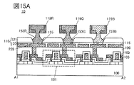
- 15A and 15B are cross-sectional views illustrating a method for manufacturing a pixel region using an inkjet method of one embodiment of the present invention.
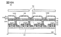
- 16A and 16B are cross-sectional views illustrating a method for manufacturing a pixel region using an evaporation method of one embodiment of the present invention.
- FIG. 17 is a perspective view showing a pixel region of one embodiment of the present invention.
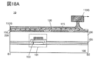
- 18A is a cross-sectional view illustrating a method for manufacturing a pixel region using an inkjet method of one embodiment of the present invention
- FIG. 18B is a cross-sectional view illustrating a method for manufacturing a pixel region using an evaporation method of one embodiment of the present invention.
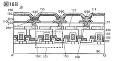
- FIG. 19A is a top view showing a pixel region of one embodiment of the present invention
- FIGS. 19B and 19C are cross-sectional views showing the pixel region.
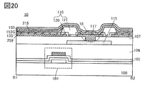
- FIG. 20 is a cross-sectional view showing a pixel region of one embodiment of the present invention.
- 21A and 21B are cross-sectional views illustrating a method for manufacturing a pixel region using an inkjet method of one embodiment of the present invention.
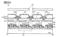
- 22A and 22B are cross-sectional views illustrating a method for manufacturing a pixel region using an evaporation method of one embodiment of the present invention.
- 23A is a cross-sectional view illustrating a method for manufacturing a pixel region using an inkjet method of one embodiment of the present invention, and FIG.
- 23B is a cross-sectional view illustrating a method for manufacturing a pixel region using an evaporation method of one embodiment of the present invention.
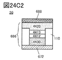
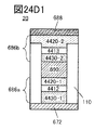
- 24A to 24D2 are cross-sectional views illustrating a light-emitting device of one embodiment of the present invention.
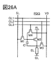
- 25A to 25D are circuit diagrams illustrating pixel circuits of one embodiment of the present invention.
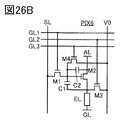
- 26A to 26D are circuit diagrams illustrating pixel circuits of one embodiment of the present invention.
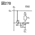
- 27A and 27B are circuit diagrams illustrating pixel circuits of one embodiment of the present invention.
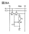
- 28A and 28B are circuit diagrams illustrating pixel circuits of one embodiment of the present invention.
- FIG. 29 is a diagram illustrating a method for driving a pixel circuit of one embodiment of the present invention.
- FIG. 30 is a perspective view showing a display device of one embodiment of the present invention.
- FIG. 31A is a cross-sectional view showing a display device of one embodiment of the present invention
- FIG. 31B is a cross-sectional view showing a transistor of one embodiment of the present invention.
- FIG. 32 is a cross-sectional view showing a display device of one embodiment of the present invention.
- FIG. 33 is a cross-sectional view illustrating a display device of one embodiment of the present invention.
- FIG. 34A is a cross-sectional view showing a display device of one embodiment of the present invention, and FIG. 34B is a cross-sectional view showing a transistor of one embodiment of the present invention.
- FIG. 35 is a cross-sectional view showing a display device of one embodiment of the present invention.
- FIG. 36 is a cross-sectional view showing a display device of one embodiment of the present invention.
- 37A and 37B are diagrams illustrating an electronic device of one embodiment of the present invention.
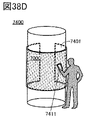
- 38A to 38D are diagrams illustrating an electronic device of one embodiment of the present invention.
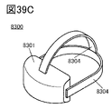
- 39A to 39F are diagrams illustrating electronic devices of one embodiment of the present invention.
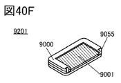
- 40A to 40F illustrate an electronic device of one embodiment of the present invention.
- the source and drain of a transistor are interchanged depending on the polarity of the transistor and the level of the potential applied to each terminal.
- a terminal to which a low potential is applied is called a source
- a terminal to which a high potential is applied is called a drain
- a terminal to which a high potential is applied is called a source.
- the terms source and drain may be interchanged depending on the potential relationship, but in this specification and the like, when describing the connection relationship between transistors, the terms source and drain are fixed for convenience.
- a source of a transistor means a source region of a semiconductor layer functioning as an active layer or a source electrode connected to the semiconductor layer.
- the drain of a transistor means the drain region of the semiconductor layer or the drain electrode connected to the semiconductor layer.
- a gate of a transistor means a gate electrode.
- a state in which transistors are connected in series means, for example, a state in which only one of the source and drain of a first transistor is connected to only one of the source and drain of a second transistor.
- a state in which transistors are connected in parallel means that one of the source and drain of the first transistor is connected to one of the source and drain of the second transistor, and the other of the source and drain of the first transistor is connected to It means the state of being connected to the other of the source and the drain of the second transistor.
- connection may be referred to as electrical connection, and includes a state in which current, voltage, or potential can be supplied, or a state in which current, voltage, or potential can be transmitted. Therefore, it also includes a state in which they are connected to each other through elements such as wiring, resistors, diodes, and transistors.
- the electrical connection includes a state of direct connection without an element such as a wiring, resistor, diode, or transistor.
- a conductive layer may have multiple functions such as a wiring or an electrode.
- the description that the wiring is connected to the electrode includes the case where there is one conductive layer having both functions as described above.
- a light-emitting device is sometimes referred to as a light-emitting element.
- a light-emitting device in which a light-emitting layer is formed using a metal mask (MM) is sometimes referred to as a light-emitting device having a metal mask (MM) structure.
- a metal mask is sometimes referred to as a fine metal mask (FMM, high-definition metal mask) as the opening becomes finer.
- FMM fine metal mask
- a light-emitting device in which a light-emitting layer is manufactured without using a metal mask or fine metal mask is sometimes referred to as a light-emitting device having a metal maskless (MML) structure.
- MML metal maskless
- a structure in which the light-emitting layers are separately painted may be referred to as an SBS (Side-By-Side) structure.
- SBS Side-By-Side
- a white light-emitting device capable of emitting white light
- the white light-emitting device can be combined with a colored layer (for example, a color filter) to form a full-color display device.
- light-emitting devices can be broadly classified into a single structure and a tandem structure.
- a single structure preferably has one light-emitting unit between a pair of electrodes, and the light-emitting unit includes one or more light-emitting layers. Therefore, the light-emitting unit is sometimes referred to as an EL layer.
- two or more light emitting layers should have a complementary color relationship. For example, by making the luminescent color of the first luminescent layer and the luminescent color of the second luminescent layer have a complementary color relationship, it is possible to obtain a configuration in which the entire light emitting device emits white light. Also, in the case of a light-emitting device having three or more light-emitting layers, a structure that emits white light can be obtained by satisfying the complementary color relationship.
- the tandem structure preferably has two or more light-emitting units between a pair of electrodes, and each light-emitting unit includes one or more light-emitting layers.
- each light-emitting unit includes one or more light-emitting layers.
- an intermediate layer such as a charge generating layer between the plurality of light emitting units.
- white light emission in order to obtain white light emission in the tandem structure, a structure in which white light emission is obtained by combining light from the light emitting layers of two or more light emitting units may be employed.
- the structure that can emit white light it suffices to satisfy the complementary color relationship as in the case of the single structure.
- the white light emitting device when comparing the white light emitting device (single structure or tandem structure) and the light emitting device having the SBS structure, the light emitting device having the SBS structure can consume less power than the white light emitting device. If it is desired to keep power consumption low, it is preferable to use a light-emitting device with an SBS structure. On the other hand, the white light emitting device is preferable because the manufacturing process is simpler than that of the SBS structure light emitting device, so that the manufacturing cost can be lowered or the manufacturing yield can be increased.
- a pixel region 10 of the display device has a plurality of pixels.
- a pixel is a minimum unit that has at least a light-emitting device and can emit light of one color. Such pixels are sometimes referred to as sub-pixels.
- a light-emitting device has a pair of electrodes and a layer (referred to as an organic material layer or an organic compound layer) having an organic material including a light-emitting layer or the like between a pair of electrodes.
- a layer referred to as an organic material layer or an organic compound layer
- an organic material layer or an organic compound layer is a laminate of functional layers such as a light-emitting layer, and is sometimes referred to as a light-emitting unit or an EL layer that can be positioned between a pair of electrodes.
- an organic compound is often used as the functional layer, it is referred to as an organic material layer or an organic compound layer, but at least one of the functional layers may be a layer containing an inorganic material (referred to as an inorganic material layer or an inorganic compound layer).
- Functional layers include a carrier injection layer (hole injection layer and electron injection layer), a carrier transport layer (hole transport layer and electron transport layer), and the like, in addition to the light-emitting layer.
- a hole injection layer refers to a layer containing a substance having a high hole injection property.
- An electron injection layer refers to a layer containing a substance with high electron injection properties.
- a hole-transporting layer refers to a layer containing a highly hole-transporting substance.
- An electron-transporting layer refers to a layer containing a substance having a high electron-transporting property.
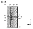
- FIG. 1A illustrates a case where the pixel region 10 has a pixel 11R capable of exhibiting red, a pixel 11G capable of exhibiting green, and a pixel 11B capable of exhibiting blue.
- Ordinal numbers may be added to distinguish the pixels, for example, ordinal numbers may be added to indicate the first red pixel and the second red pixel.
- the X direction and the Y direction intersecting with the X direction may be used as shown in FIG. 1A.
- the pixels 11R, 11G, and 11B are arranged in order in the X direction, and a plurality of pixels 11R are arranged in the Y direction.
- a plurality of pixels 11B and 11G are similarly arranged in the Y direction.
- the pixel 11G is positioned in the region adjacent to the pixel 11R in the X direction
- another pixel 11R is positioned in the region adjacent to the pixel 11R in the Y direction.
- Pixel 11R has at least contact hole 15R.
- the contact hole 15R is an opening provided in the insulating layer positioned between the light emitting device and the transistor to ensure electrical connection between the light emitting device and the transistor that drives the light emitting device.
- pixel 11G has at least contact hole 15G and pixel 11B has at least contact hole 15B.
- the pixel area 10 has an auxiliary electrode 115 as shown in FIG. 1A.
- the auxiliary electrode is a layer having an auxiliary function of the main electrode, and the auxiliary function includes lowering the resistance of the main electrode.
- the auxiliary electrode is formed using at least a conductive material to reduce the resistance of the main electrode. Furthermore, the resistivity of the conductive material of the auxiliary electrode is preferably lower than that of the conductive material of the main electrode.
- the resistance of the main electrode can also be reduced by the auxiliary electrode by making the area of the auxiliary electrode larger than that of the main electrode, or by making the thickness of the auxiliary electrode thicker than that of the main power supply.
- An auxiliary electrode may be described as an auxiliary wiring based on its shape, but in this specification and the like, the auxiliary electrode will be used for explanation.
- FIG. 1A shows the case where the auxiliary electrode 115 is arranged between each pixel in the pixel region 10 .
- the auxiliary electrode 115 has regions extending in the X direction and the Y direction, and has a lattice shape when viewed from above.
- the arrangement of the auxiliary electrodes is not limited to the above-described grid pattern, and may be arranged so as to reduce the resistance of the main electrodes.
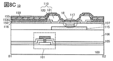
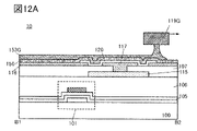
- the pixel region 10 has contact holes 18 .
- the contact hole 18 is an opening provided in the insulating layer positioned between the auxiliary electrode 115 and the upper electrode 159 in order to ensure electrical connection between the auxiliary electrode 115 and the upper electrode 159 of the light emitting device. .
- the upper electrode 159 will be described later.
- the top surface shape of the contact hole 18 is preferably made larger than the contact hole 15R and the like of each pixel.
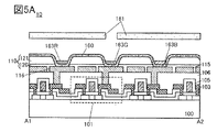
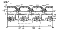
- FIG. 1B1 shows a cross-sectional view corresponding to A1-A2 passing through contact hole 15R, contact hole 15G and contact hole 15B in FIG. 1A.
- a cross-sectional view corresponding to B1-B2 passing through the contact hole 18 in FIG. 1A is shown in FIG. 1C.
- Transistor 101> 1B1 and 1C show an example with a transistor 101 on a substrate 100.
- FIG. A transistor 101 is an element for driving a light-emitting device (referred to as a driving element).
- a display device having the driving element in each pixel is referred to as an active matrix display device.
- the transistor 101 has at least a semiconductor layer, a gate 102, a source and a drain 103, and FIG. 1B1 illustrates a top-gate transistor in which the gate 102 is located on the semiconductor layer as the transistor 101.
- FIG. 1B1 illustrates a top-gate transistor in which the gate 102 is located on the semiconductor layer as the transistor 101.
- a bottom-gate transistor whose gate is located under the semiconductor layer may be applied, or a dual-gate transistor whose gates are located above and below the semiconductor layer may be applied.
- a gate insulating layer is positioned between the gate 102 and the semiconductor layer.
- the semiconductor layer can be formed using silicon or an oxide semiconductor, and may be crystalline or amorphous.
- regions in contact with the source and drain 103 are called impurity regions, and an element other than silicon (referred to as an impurity element) such as phosphorus or boron is added to lower the resistance.
- an impurity element such as phosphorus or boron is added to lower the resistance.
- the impurity region is also referred to as a low-resistance region).
- a single-layer structure of a conductive layer or a laminated structure of conductive layers can be applied to the source and drain 103 .
- the conductive layer comprises an electrically conductive material, the electrically conductive material comprising aluminum, titanium, copper, tungsten, molybdenum, or nickel.
- a conductive layer containing titanium, a conductive layer containing aluminum, and a conductive layer containing titanium are preferably used.
- the gate 102 can have a single-layer structure of conductive layers or a laminated structure of conductive layers.
- the conductive layer comprises an electrically conductive material, the electrically conductive material comprising aluminum, titanium, copper, tungsten, molybdenum, or nickel.
- a conductive layer containing molybdenum and a conductive layer containing tungsten are preferably used.
- the gate 102 is covered with at least an insulating layer 105 .
- the source and drain 103 can each have a region in contact with the semiconductor layer through the opening provided in the gate insulating layer and the opening provided in the insulating layer 105 . Note that in FIG. 1C, it can be confirmed that one of the source and the drain 103 is in contact with the semiconductor layer.
- the gate insulating layer and insulating layer 105 preferably contain an inorganic material.
- the insulating layer 105 contains an inorganic material, entry of an impurity element into the semiconductor layer can be suppressed.
- a material obtained by adding an impurity element such as lanthanum (La), nitrogen, or zirconium (Zr) to the above material may be used.
- An insulating layer 106 is provided over the insulating layer 105 .
- the upper surface of the insulating layer 106 preferably has flatness because it corresponds to a surface on which a lower electrode of a light-emitting device to be formed later is formed.
- the insulating layer 106 is formed using an organic material, the above flatness can be provided.
- an organic resin such as a polyimide resin, a polyamide resin, an acrylic resin, a siloxane resin, a silicone resin, an epoxy resin, or a phenol resin is preferably used.
- a material obtained by adding an impurity element such as lanthanum, nitrogen, or zirconium to the above material may be used.
- Transistor application example A cross-sectional structure example of a transistor that can be applied to the transistor 101 is described.
- FIG. 2A is a cross-sectional view including transistor 101 .
- the transistor 101 a transistor which is provided over the substrate 100 and whose semiconductor layer is formed using polycrystalline silicon having crystallinity can be used. At this time, the transistor 101 can be called an LTPS transistor.
- the transistor 101 includes a semiconductor layer 311, an insulating layer 312, a conductive layer 313, and the like.
- the semiconductor layer 311 has a channel forming region 311i and a low resistance region 311n. At least the channel forming region 311i comprises silicon, preferably polycrystalline silicon.
- a portion of the insulating layer 312 functions as a gate insulating layer.
- a region of the conductive layer 313 overlapping with the semiconductor layer 311 functions as a gate.
- the semiconductor layer 311 can also have a structure using an oxide semiconductor (also referred to as a metal oxide exhibiting semiconductor characteristics).
- the transistor includes an oxide semiconductor at least in a channel formation region.
- the transistor 101 can be referred to as an OS transistor, and the semiconductor layer is sometimes referred to as an oxide semiconductor layer.
- the transistor 101 includes a conductive layer 314a, a conductive layer 314b, and the like.
- Conductive layer 314a can function as one of source and drain
- conductive layer 314b can function as one of source and drain.
- One of the source and drain of transistor 101 can be electrically connected to the bottom electrode 116 of the light emitting device.
- one of the conductive layers 314a and 314b can be electrically connected to a lower electrode 116, which will be described later, and a contact hole can be formed in, for example, the insulating layer 323 located therebetween.
- An insulating layer 321 may be provided between the substrate 100 and the transistor 101, and the semiconductor layer 311 is provided over the insulating layer 321 in FIG. 2A.
- the contents described with reference to FIG. 1 can be applied.
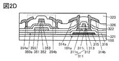
- FIG. 2B shows transistor 101a with a pair of gates.
- a transistor 101a shown in FIG. 2B is mainly different from FIG.
- the conductive layer 315 is provided over the insulating layer 321 .
- An insulating layer 316 is provided to cover the conductive layer 315 and the insulating layer 321 .
- the semiconductor layer 311 is provided so that at least the channel formation region 3111 overlaps with the conductive layer 315 with the insulating layer 316 interposed therebetween.
- part of the conductive layer 313 functions as a first gate and part of the conductive layer 315 functions as a second gate.
- part of the insulating layer 312 functions as a first gate insulating layer
- part of the insulating layer 316 functions as a second gate insulating layer.
- the conductive layers 313 and 315 are connected through openings provided in the insulating layers 312 and 316 in a region (not shown). should be electrically connected.
- the conductive layer 314a is formed through openings provided in the insulating layers 322, 312, and 316 in a region (not shown).
- the conductive layer 314b and the conductive layer 315 may be electrically connected.
- the conductive layer 314a can function as one of the source and the drain
- the conductive layer 314b can function as one of the source and the drain.
- One of the source and drain of transistor 101 can be electrically connected to the bottom electrode 116 of the light emitting device.
- one of the conductive layers 314a and 314b can be electrically connected to a lower electrode 116, which will be described later, and a contact hole can be formed in, for example, the insulating layer 323 located therebetween.
- the transistor 101 illustrated in FIG. 2A or the transistor 101a illustrated in FIG. 2B can be applied.
- an OS transistor is used as a transistor such as the pixel 11R illustrated in FIG. 1, the transistor 101 illustrated in FIG. 2A or the transistor 101a illustrated in FIG. 2B can be used.
- the pixel 11R and the like illustrated in FIG. 1 are provided with a plurality of transistors. may be applied to a pixel.
- an LTPS transistor can be used as the transistor 101 and an OS transistor can be used as the transistor 101a.
- FIG. 2C illustrates a cross-sectional view that includes multiple transistors.
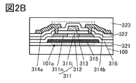
- FIG. 2C A cross-sectional view, including transistor 101a and transistor 350, is shown in FIG. 2C.
- the right side of FIG. 2C shows a transistor 101a, which can be an LTPS transistor.
- a transistor 350 is shown on the left side of FIG. 2C, and the transistor 350 can be an OS transistor. Both the transistor 101a and the transistor 350 have a pair of gates, but some gate positions are different.
- the transistor 101a has an insulating layer 326 not shown in FIG. 2B, but the description of FIG. 2B can be referred to for other configurations. Also in the transistor 101a illustrated in FIG. 2C, one of the conductive layers 314a and 314b can be electrically connected to the lower electrode 116, and a contact hole is formed in the insulating layer 323 between them, for example. be able to.
- the transistor 350 includes a conductive layer 355, an insulating layer 322, a semiconductor layer 351, an insulating layer 352, a conductive layer 353, and the like.
- a portion of conductive layer 353 functions as a first gate of transistor 350 and a portion of conductive layer 355 functions as a second gate of transistor 350 .
- part of the insulating layer 352 functions as a first gate insulating layer of the transistor 350 and part of the insulating layer 322 functions as a second gate insulating layer of the transistor 350 .
- a conductive layer 355 is provided over the insulating layer 312 .
- An insulating layer 322 is provided to cover the conductive layer 355 .
- the semiconductor layer 351 is provided over the insulating layer 322 .
- the insulating layer 352 is provided to cover the semiconductor layer 351 and the insulating layer 322 .
- the conductive layer 353 is provided over the insulating layer 352 and has regions overlapping with the semiconductor layer 351 and the conductive layer 355 .
- An insulating layer 326 is provided to cover the insulating layer 352 and the conductive layer 353 .
- a conductive layer 354 a and a conductive layer 354 b are provided over the insulating layer 326 .
- the conductive layers 354 a and 354 b are electrically connected to the semiconductor layer 351 through openings provided in the insulating layers 326 and 352 .
- Conductive layer 354a functions as one of the source and drain, and conductive layer 354b functions as the other of the source and drain.
- An insulating layer 323 is provided to cover the conductive layers 354 a , 354 b , and the insulating layer 326 .
- the conductive layers 314a and 314b of the transistor 101a are preferably formed by processing the same conductive film as the conductive layers 354a and 354b.
- the conductive layer 314a, the conductive layer 314b, the conductive layer 354a, and the conductive layer 354b are formed over the same formation surface (specifically, the top surface of the insulating layer 326) and contain the same metal element. showing configuration.
- the conductive layers 314a and 314b can be electrically connected to the low-resistance region 311n through contact holes provided in the insulating layers 326, 352, 322, and 312. can. This is preferable because the manufacturing process can be simplified.
- the conductive layer 313 functioning as the first gate of the transistor 101a and the conductive layer 355 functioning as the second gate of the transistor 350 are preferably formed by processing the same conductive film.
- FIG. 2C shows a structure in which the conductive layers 313 and 355 are formed over the same formation surface (specifically, the top surface of the insulating layer 312) and contain the same metal element. This is preferable because the manufacturing process can be simplified.
- the insulating layer 352 functioning as a first gate insulating layer of the transistor 350 covers the semiconductor layer 351; It may be processed so that the upper surface shape is approximately the same.
- a lower electrode 116 is formed on the insulating layer 106 .
- the lower electrode 116 corresponds to the lower electrode of the pair of electrodes of the light-emitting device, and functions as an anode, for example.
- the lower electrode 116 is located on the transistor 101 side and is electrically connected to the transistor 101 so that a signal can be applied from the transistor 101 to the light emitting device. Since the signal is different for each pixel, the lower electrode 116 is processed so as to be independent for each pixel. This processing is sometimes referred to as patterning.
- Each of the pixels 11R, 11G, and 11B has a lower electrode 116, and an ordinal number may be assigned to distinguish each lower electrode 116. For example, a first lower electrode and a second lower electrode are used. Also, the lower electrode 116 may be referred to as a pixel electrode.
- the shape of the upper surface of the lower electrode 116 is not limited, in FIG. 1A, the lower electrode 116 has a rectangular shape, and has a short side along the X direction and a long side along the Y direction.
- a tapered shape refers to a shape in which at least part of the side surface of the structure is inclined with respect to the formation surface or the substrate surface.
- the angle formed by the inclined side surface and the substrate surface is called a taper angle
- the taper shape refers to a region where the taper angle is less than 90°.
- the side surface of the structure may be substantially planar with a fine curvature or substantially planar with fine unevenness.
- the taper angle can also be measured by providing a line from the top to the bottom of the side of the structure.
- the surface to be formed or the substrate surface may be substantially planar with a fine curvature or substantially planar with fine unevenness.
- the taper angle of the end portion of the lower electrode 116 is preferably 35 degrees or more and less than 90 degrees, preferably 40 degrees or more and 80 degrees or less.
- FIG. 1B1 has openings formed in insulating layer 106 as contact hole 15R, contact hole 15G, and contact hole 15B, respectively.
- Each contact hole has a region where one of the source and drain 103 and the lower electrode 116 are in contact.
- another conductive layer may be interposed between one of source and drain 103 and lower electrode 116, for example. That is, one of the source/drain 103 and the lower electrode 116 may be structured so as not to be in contact with each other.
- the lower electrode 116 functions as an anode, it is preferable to use a material with a large work function. Therefore, the lower electrode 116 is an ITO film (an oxide film containing indium and tin), an indium tin oxide film containing silicon, an indium oxide film containing 2 wt % or more and 20 wt % or less of zinc oxide, a titanium nitride film, or chromium. film, tungsten film, Zn film, Pt film, Cu film, Al film, etc., laminated structure of titanium nitride film and aluminum-based film, titanium nitride film and aluminum-based film. A laminated structure of a film and a titanium nitride film or the like can be used.
- the film containing aluminum as the main component may contain nickel, tungsten, or a rare earth element (for example, lanthanum) in addition to aluminum.
- a rare earth element for example, lanthanum
- one layer can be formed using a low-resistance material, and the other layer can be formed using a material capable of making good ohmic contact with one of the source and drain 103, which is preferable. It is preferable that the thickness of the entire lower electrode 116 is set to 100 nm or more and 250 nm or less.
- the lower electrode 116 In the case of a display device in which light from the light-emitting device is extracted from the lower electrode 116 side, the lower electrode 116 needs to be translucent.
- a light-transmitting material is selected from the materials described above, or when a non-light-transmitting material is selected, a structure such as a thin film is adopted.
- the auxiliary electrode 115 is formed using the same material as the lower electrode 116 . 1B1 and 1C have an auxiliary electrode 115 on an insulating layer 106 with a bottom electrode 116 provided thereon. The auxiliary electrode 115 must be processed so as not to have the same potential as the lower electrode 116, that is, be independent of each other. An example of independent placement is shown in FIG. 1A.
- the auxiliary electrodes 115 are arranged in a shape having regions extending in the X-direction and the Y-direction, that is, in a grid pattern, using the spaces between the pixels 11R, 11G and 11B.
- the distance between the lower electrode 116 and the auxiliary electrode 115 in the region along the Y direction is preferably larger than the distance between the lower electrode 116 and the auxiliary electrode in the region along the X direction.
- the auxiliary electrode 115 enables electrical connection with the upper electrode 159 of the subsequently formed light emitting device.
- the auxiliary electrode 115 can reduce the resistance of the upper electrode 159 and suppress the voltage drop.
- Partition 110 When an organic material layer or an organic compound layer, such as a light-emitting layer, is separately coated by a wet method such as an inkjet method, a section for dropping a solution is required.
- the compartments may be formed by insulation, and such insulation is sometimes referred to as a partition, embankment, or bank.
- the insulator When each light-emitting layer is formed by vapor deposition, the insulator may have the function of holding a metal mask, specifically a fine metal mask.
- the wet method is a method of dissolving or dispersing a material having a predetermined function in a solvent to liquefy the material to obtain a liquid composition, and applying the liquid composition.
- a material having a predetermined function includes a hole-injecting material, a hole-transporting material, a light-emitting material, an electron-transporting material, or an electron-injecting material.
- Liquid compositions are sometimes referred to as droplets or ink materials.
- the liquid composition is solidified or thinned through a drying process or a curing process, whereby the organic material layer or organic compound layer can be obtained.
- each material becomes a hole injection layer, a hole transport layer, a light emitting layer, an electron transport layer, or an electron injection layer.
- the liquid composition is often referred to as a droplet, but the liquid composition may be referred to as an ink material. Also, although it may be described as dropping a droplet, it may be described as applying an ink material.
- Wet methods include inkjet methods, spin coating methods, coating methods, inkjet nozzle printing methods, gravure printing, and the like.
- a material formed by an inkjet method preferably includes a polymer material (also referred to as a polymer-based organic material).
- a polymer material also referred to as a polymer-based organic material.
- a polymeric material containing a light-emitting material is sometimes referred to as a polymer-based light-emitting organic material.
- a polymeric material is preferable because it is easily mixed with a solvent. Toluene, xylene, and the like are among the above-mentioned solvents that are easily mixed with the polymer material.
- the partition 110 is formed on the lower electrode 116 and the auxiliary electrode 115 .
- the partition is abbreviate
- the partition wall 110 covers the edge of the lower electrode 116 and has an opening to expose the central portion of the lower electrode 116 .
- the partition wall 110 covers the entire auxiliary electrode 115 .
- the contact hole 18 formed in the partition wall 110 can be confirmed.
- the partition 110 has a first partition (referred to as a first insulator) 120 and a second partition (referred to as a second insulator) 121, and has a stacked structure of these. do it.
- the first insulator 120 may have an inorganic material
- the second insulator 121 may have an organic material. It is preferable to use an organic material for the second insulator 121 because the height of the partition 110 can be increased.
- the first insulator 120 may also have an organic material to increase the height of the partition 110 .
- the inkjet device can be moved along the tall partition wall 110 .
- the high barrier ribs 110 can suppress color mixing with a different color material.
- Inorganic materials included in the partition 110 include aluminum oxide, magnesium oxide, silicon oxide, silicon oxynitride, silicon nitride oxide, silicon nitride, gallium oxide, germanium oxide, yttrium oxide, zirconium oxide, lanthanum oxide, neodymium oxide, hafnium oxide, and tantalum oxide. should include one or more of When the partition 110 has a layered structure, the first insulator 120 or the second insulator 121 preferably contains the above inorganic material.
- the organic material included in the partition 110 is preferably an organic resin such as polyimide resin, polyamide resin, acrylic resin, siloxane resin, silicone resin, epoxy resin, or phenol resin.
- the second insulator 121 preferably contains the above organic material. If the partition wall 110 is desired to be high, the first insulator 120 may have the above organic material.
- a material obtained by adding an impurity element such as lanthanum (La), nitrogen, or zirconium (Zr) to the above inorganic material or organic material may be used.
- the partition wall 110 has a structure that partitions each pixel, that is, has a lattice shape having regions extending in the X direction and the Y direction. That is, the partition 110 is provided in a region overlapping with the auxiliary electrode 115 .
- the upper end of the partition 110 may be rounded as shown in FIG. 1B1. Being rounded is sometimes described as having a curvature. Note that at least the upper end portion of the second insulator 121 in the partition 110 should have a curvature. When the opening is formed, the lower end of the partition 110 can be curved. In addition, in the partition 110, at least the lower end portion of the first insulator 120 should have a curvature.
- the ends of the partition walls 110 are preferably tapered.
- the partition wall 110 may have a structure in which the diameter of the lower surface is longer than the diameter of the upper surface, and the ends may be tapered to form a forward tapered shape.
- the partition wall 110 may have a structure in which the diameter of the lower surface is smaller than the diameter of the upper surface, and the ends may be tapered to form an inverse tapered shape. Both tapered shapes are common in that the ends of the partition walls 110 are slanted. When the ends are slanted, the solution from the inkjet can be dropped into the target pixel, thereby suppressing color mixture.
- the partition 110 when the thickness of the second insulator 121 is larger than the thickness of the first insulator 120, at least the end portion of the second insulator 121 may be inclined.
- the taper angle of the end portion of the partition wall 110 may be obtuse than the taper angle of the end portion of the lower electrode 116, preferably 15 degrees or more and 70 degrees or less, preferably 20 degrees or more and 60 degrees or less.
- a layer 150 is formed over the bottom electrode 116, as shown in FIGS. 1B1 and 1C.
- Layer 150 is located between lower electrode 116 and light-emitting layers 153R, 153G, and 153B, which will be described later, and can inject holes from lower electrode 116 into light-emitting layers 153R, 153G, and 153B.
- the layer 150 may have a structure having a hole injection layer, a structure having a hole transport layer, or a structure in which a hole injection layer and a hole transport layer are laminated in order from the lower electrode 116 .
- Ordinal numbers may be used to distinguish the layers 150, eg, first layer, second layer.
- Layer 150 is preferably formed by, for example, a wet method.
- Wet methods include spin coating, inkjet, casting, printing, dispensing, or spraying.
- productivity can be improved.
- a structure in which at least layer 150 is formed by a wet method is suitable for a flexible display device.
- FIG. 1B2 the film thickness of the layer 150 formed by the wet method will be described using an enlarged view of the region marked with a circle and an arrow in FIG. 1B1, that is, the end of the partition 110.
- FIG. A first insulator 120 and a second insulator 121 are shown in FIG. 1B2.
- the distance from the center (C) to the edge of the layer 150 is L1.
- the side opposite the edge of layer 150 from the center (C) is marked with the same distance L1 to indicate the range of distance L1 from the center (C).
- the range of the distance L1 may be referred to as a vicinity area of the partition wall.
- the film thickness of the layer 150 is thicker in the vicinity of the partition than in the center of the light emitting area. That is, the film may be thickened in the vicinity of the partition wall. This thickened portion is sometimes referred to as a liquid puddle.
- the thickness of layer 150 is often the thickest in the region overlapping the center (C). It can be said that the layer 150 thickened in the vicinity of the partition wall is produced by a wet method.
- the layer 150 may be formed over the entire pixel area 10 without being divided for each pixel. That is, the layer 150 can be formed over a plurality of bottom electrodes and common to each pixel. Layer 150 can be formed by a wet method or a vapor deposition method. The layer 150 that can be shared by pixels is preferably formed by a spin coating method or an evaporation method.
- the layer 150 may be separated at each pixel by a partition wall 110 .
- a structure in which the layer 150 is not located on the upper surface of the partition 110 can be obtained by subjecting the upper surface of the partition 110 to liquid-repellent treatment.
- a structure in which the layer 150 is not located on the upper surface of the partition wall 110 can be obtained by vapor deposition using a metal mask.
- a light-emitting layer 153R, a light-emitting layer 153G, and a light-emitting layer 153B are separately formed over the layer 150 by painting.
- the shaded structure corresponds to the SBS structure.
- the luminescent colors of the luminescent layer 153R, the luminescent layer 153G, and the luminescent layer 153B correspond to red, green, and blue, respectively, enabling full-color display.
- Light-emitting layer 153R, light-emitting layer 153G, and light-emitting layer 153B are preferably formed by a wet method similar to layer 150, for example.
- Wet methods include spin coating, inkjet, casting, printing, dispensing, or spraying.
- Productivity can be improved by forming at least the light-emitting layer by a wet method.
- a structure in which at least the light-emitting layer is formed by a wet method is suitable for a flexible display device.
- the film thickness of the layer 150 has been described with reference to FIG. That is, the film thicknesses of the light-emitting layers 153R, 153G, and 153B are larger in the vicinity of the partition wall than in the central region of the light-emitting area of the partition wall.
- the luminescent layers 153R, 153G, and 153B which are thickened in the vicinity of the partition wall, are produced by a wet method.
- FIGS. 4A and 4B An inkjet device that can be used for the inkjet method is shown in FIGS. 4A and 4B.
- FIG. 4A shows formation of the light-emitting layer 153R, light-emitting layer 153G, and light-emitting layer 153B
- FIG. 4B shows formation of the light-emitting layer 153G.
- the inkjet apparatus shown in FIGS. 4A and 4B may be used to form the layer 150, and the same inkjet apparatus may be used to form the layer 150 and the light-emitting layers 153R, 153G, and 153B. .
- productivity can be improved.
- FIGS. 4A and 4B show inkjet nozzles 119R, 119G, and 119B that the inkjet device has.
- the opening diameters of the inkjet nozzles 119R, 119G, and 119B are several micrometers or more and several tens of micrometers or less.
- a portion having inkjet nozzles is sometimes referred to as a head.
- the head In order to drop the solution, the head is provided with a solution injection control unit, and additionally has a piezoelectric element (piezo element) and the like.
- a pressure element can change the volume of an ink tank connected to an inkjet nozzle to cause the solution to drop from the head.
- the amount of one droplet is often several pl or more and several tens of pl or less depending on the ink jet nozzle diameter. Although it depends on the material, 1 pl of the solution can be considered as an amount for forming a cube with a side of about 10 ⁇ m.
- the solution may be intermittently dripped from inkjet nozzles 119R, 119G, and 119B. Alternatively, the solution may be linearly and continuously dropped from the inkjet nozzles 119R, 119G, and 119B.
- FIG. 4A shows a cross-sectional view of the light-emitting layer 153G, showing a state before the inkjet nozzle 119R, which can move in the direction of the arrow, climbs over the partition wall 110.
- FIG. 1 and the like can be referred to for other configurations.
- a liquid pool is confirmed near the partition wall 110 .
- the liquid pool can refer to the description using FIG. 1B2 above, and the liquid pool corresponds to a portion where the light-emitting layer 153R, the light-emitting layer 153G, the light-emitting layer 153B, or the layer 150 is thickened in the vicinity of the partition wall 110. .
- the liquid pool is caused by a drying process in a normal pressure atmosphere or a reduced pressure atmosphere, which is performed to remove the solvent. Especially in the drying process in a reduced pressure atmosphere, a liquid pool occurs due to a phenomenon in which the solute gathers outside with the driving force of the surface tension of the solution. When such a liquid pool is confirmed, it can be understood that the layer is formed by a wet method such as an inkjet method.
- At least the light-emitting layer can be separately painted without using a metal mask.
- the light-emitting layer 163R, the light-emitting layer 163G, and the light-emitting layer 163B may be formed by vapor deposition.
- FIGS. 5A and 5B show how the light-emitting layer 163R, the light-emitting layer 163G, and the light-emitting layer 163B are formed using a vapor deposition method.
- Layer 160 located below light-emitting layer 163R, light-emitting layer 163G, and light-emitting layer 163B can also be formed using a vapor deposition method, but in FIG. 5A layer 160 is formed by a wet method. Since the layer 160 is shared by each pixel, it is preferably formed by a spin coating method. In FIGS. 5A and 5B, other configurations can be referred to FIG. 1 and the like.
- the metal mask 161 is shown in FIGS. 5A and 5B.
- FIGS. 5A and 5B show how a light-emitting layer 163G and the like are formed using a metal mask 161 having openings overlapping pixels of the same color.
- a metal mask 161 can be shifted by the remaining colors, for example, two or more times to form each light-emitting layer.
- a fine metal mask can be used as the metal mask 161 .
- a light-emitting device having the light-emitting layer can be said to have an MM structure.
- the light-emitting layer is preferably formed by a wet method such as an inkjet method because of its high productivity, but it may be formed by a vapor deposition method.
- Layer 155 is then formed as shown in FIGS. 1B1 and 1C.
- Layer 155 is located between upper electrode 159 and light-emitting layers 153R, 153G, and 153B, and can inject electrons from upper electrode 159 into light-emitting layers 153R, 153G, and 153B.
- the layer 155 may have a structure having an electron injection layer, a structure having an electron transport layer, or a structure in which an electron injection layer and an electron transport layer are laminated in order from the upper electrode 159 .
- layer 155 may be formed over the entire pixel area 10 without being segmented for each pixel.
- Layer 150 is formed over a plurality of light-emitting layers and can be shared by each pixel.
- Layer 155 can be formed by a wet method or a vapor deposition method. Wet methods include spin coating, inkjet, casting, printing, dispensing, or spraying.
- the layer 155 that can be shared by pixels is preferably formed by a spin coating method or an evaporation method.
- a top electrode 159 is formed over layer 155 .
- the upper electrode 159 corresponds to the upper electrode of the pair of electrodes of the light emitting device, and functions as a cathode, for example. Also, the upper electrode 159 may be referred to as a counter electrode.
- the upper electrode 159 may be formed over the entire pixel region 10 without dividing it for each pixel.
- the upper electrode 159 is formed over a plurality of light emitting layers and can be shared by each pixel.
- the upper electrode 159 can be formed by a wet method or vapor deposition method. Wet methods include spin coating, inkjet, casting, printing, dispensing, or spraying.
- the upper electrode 159 that can be shared by pixels is preferably formed by a spin coating method or an evaporation method.
- the upper electrode 159 functions as a cathode, a material with a small work function (Al, Mg, Li, Ca, alloys thereof (an alloy containing Mg and Ag is referred to as MgAg, and an alloy including Mg and In is referred to as MgIn). and an alloy containing Al and Li is referred to as AlLi) or a compound thereof) is preferably used.
- a thin metal thin film can be used as the upper electrode 159.
- a transparent conductive film (ITO, indium oxide containing 2 wt % or more and 20 wt % or less of zinc oxide, indium tin oxide containing silicon, zinc oxide (ZnO), or the like) can be used. Furthermore, a laminate of a metal thin film and a transparent conductive film can be used as the upper electrode 159 .
- a contact hole 18 is formed prior to forming the top electrode 159, as shown in FIG. 1C.
- Contact hole 18 can be formed using, for example, a photolithographic method. Photolithography includes a method of forming a resist mask on a thin film to be processed, processing the thin film by etching or the like, and removing the resist mask, and a method of forming a photosensitive thin film, followed by exposure and development. and a method of processing the thin film into a desired shape. For example, after forming layer 155, a mask for forming contact hole 18 can be prepared and a resist mask can be used as the mask.
- a structure in which the light-emitting layer is not located on the upper surface of the partition wall 110 can be employed.
- the contact hole 18 when the contact hole 18 is formed, the top surface of the light-emitting layer is protected by the layer 155 and the side surface thereof is protected by the partition wall 110, so that the light-emitting layer is not exposed to the etchant.
- contact hole 18 can be formed using only a resist mask.
- a sacrificial layer (sometimes referred to as a mask layer) may be formed between the resist mask and the layer 155 in order to reduce damage to an organic material layer such as a light-emitting layer or an organic compound layer during processing.
- a sacrificial layer has a function of protecting a functional layer such as a light-emitting layer during a manufacturing process. Specifically, when processing a light-emitting device, a sacrificial layer is formed at a position where damage due to processing does not enter the light-emitting layer or the like. The sacrificial layer may be completely removed or partially left during the manufacturing process of the light-emitting device.
- the sacrificial layer is a material layer formed below (the material layer is the object of processing and may be referred to as a layer to be processed), which is protected from process damage when processing the layer by etching or the like. It is a layer provided for protection. Therefore, the sacrificial layer may be formed thicker than the layer to be processed.
- the sacrificial layer for example, a metal film, an alloy film, a metal oxide film, a semiconductor film, an inorganic insulating film, or the like can be used.
- the sacrificial layer can be formed by various film forming methods such as sputtering, vapor deposition, CVD, or ALD. Note that a formation method that causes little damage to the organic material layer or the organic compound layer is preferable, and it is preferable to form the sacrificial layer using an ALD method or a vacuum evaporation method.
- metal materials such as gold, silver, platinum, magnesium, nickel, tungsten, chromium, molybdenum, iron, cobalt, copper, palladium, titanium, aluminum, yttrium, zirconium, and tantalum, or the metal materials are used.
- a metal oxide such as indium gallium zinc oxide (also referred to as In—Ga—Zn oxide, IGZO) can be used.
- indium oxide, indium zinc oxide (In—Zn oxide), indium tin oxide (In—Sn oxide), indium titanium oxide (In—Ti oxide), indium tin zinc oxide (In—Sn -Zn oxide), indium titanium zinc oxide (In-Ti-Zn oxide), indium gallium tin zinc oxide (In-Ga-Sn-Zn oxide), or the like can be used.
- indium tin oxide containing silicon or the like can be used.
- element M is aluminum, silicon, boron, yttrium, copper, vanadium, beryllium, titanium, iron, nickel, germanium, zirconium, molybdenum, lanthanum, cerium, neodymium, hafnium, tantalum, tungsten , or one or more selected from magnesium).
- M is preferably one or more selected from gallium, aluminum, and yttrium.
- An inorganic insulating material such as aluminum oxide, hafnium oxide, or silicon oxide can be used as the sacrificial layer.
- the sacrificial layer has a laminated structure
- a layer formed of any of the above materials can be used as the first sacrificial layer, and the second sacrificial layer can be laminated thereon.
- the sacrificial layer may also be processed.
- the sacrificial layer is preferably made of a material having a high etching selectivity with respect to the organic material layer or the organic compound layer.
- a material having a high etching selectivity with respect to the partition 110 is preferably used for the sacrificial layer.
- a material that can be removed by wet etching is preferably used for the sacrificial layer.
- the organic material layer, the organic compound layer, or the like may be damaged.
- the damage can be reduced as compared with the dry etching method.
- the upper electrode 159 and the auxiliary electrode 115 can be electrically connected.
- the opening of the first insulator 120 is smaller than the opening of the second insulator 121
- the opening of the second insulator 121 is smaller than the opening of the first insulator 120 .
- the layer 155 forms the opening the earliest, the opening widens, and the edge of the layer 155 defining the opening may recede to a position overlapping the upper surface of the partition wall 110 . That is, the diameter of the opening of each layer decreases stepwise toward the lower auxiliary electrode 115 .
- the structure in which the diameter of the opening of each layer gradually decreases toward the auxiliary electrode 115 makes it difficult to cut the upper electrode 159 in the contact hole 18 (sometimes referred to as a discontinuity). preferable.
- the upper electrode 159 is electrically connected to the auxiliary electrode 115, it is preferable to partially etch the surface of the auxiliary electrode 115 (referred to as over-etching). When a part of the surface is etched, a concave portion is formed in the surface of the auxiliary electrode 115. Using the concave portion is preferable because the contact area between the auxiliary electrode 115 and the upper electrode 159 is increased.
- FIG. 1C shows a structure in which the layer 155 is not located within the contact hole 18, the layer 155 may be located within the contact hole 18.
- FIG. 3 even if the layer 155 is positioned between the auxiliary electrode 115 and the upper electrode 159 in the contact hole 18, it is sufficient if the auxiliary electrode 115 and the upper electrode 159 can be electrically connected.
- contact hole 18 prior to forming layer 155, contact hole 18 would be formed. It is preferable to dispose a sacrificial layer when forming the contact hole 18 . 1 and the like can be referred to for other configurations in FIG.
- the contact hole 18 can be provided at any location. For example, as shown in FIG. 1A, one contact hole 18 may be formed for six pixels. Since the upper electrode 159 is shared by the pixel region 10, a voltage drop is likely to occur. Therefore, the contact holes 18 need only be formed at a rate of one for a plurality of pixels, and there is no need to form the contact holes 18 at a rate of one for each pixel.
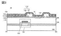
- the grid-like partition wall 110 has a first region 110x along the X direction and a second region 110y along the Y direction.
- the height of partition 110 may be different, for example, the height of first region 110x and second region 110y may be different.
- the second region 110y is higher than the first region 110x, that is, when the positions of the top surfaces of the regions are compared, the second region 110y is the second region 110y. 1 is higher than region 110x.
- the partition 110 preferably has a laminated structure in which a second insulator 121 having an organic material is positioned on a first insulator 120 having an inorganic material. It is preferable that the insulator 120 correspond to the first region 110x and the stacked structure of the first insulator 120 and the second insulator 121 correspond to the second region 110y. For example, after forming the first insulator 120 in a grid pattern, the second insulator 121 may be formed only in the portion corresponding to the second region 110y.
- the second region 110y which is a high partition, can be obtained even if the partition is formed only from an organic material.
- a partition with a thickness Hx is formed of an organic material in the X direction including the first region 110x.
- a partition having a thickness of Hy (Hy>Hx, and Hy preferably having a thickness of 1.2 to 2.5 times as large as Hx) is formed using an organic material. do.
- the partition wall 110 is the highest at the intersection of the X direction and the Y direction.
- the inkjet nozzles 119R, 119G, and 119B shown in FIG. 4 and the like can be moved along the second region 110y shown in FIG. Furthermore, the second region 110y is a tall partition wall, which can suppress color mixture. Suppression of color mixture is particularly preferable when simultaneously forming light-emitting layers having different colors with respect to the pixels 11R, 11G, and 11B.
- a first region 110x is located at the boundary between pixels of the same color.
- the first region 110x is a partition lower than the second region 110y. Therefore, for the purpose of suppressing color mixture, the light-emitting layer can be formed by an inkjet method without the first region 110x.
- the first region 110x is preferable because it can suppress liquid unevenness between the same colors.
- FIGS. 7A and 7B show cross-sectional views along the first region 110x.
- FIGS. 7A and 7B show the case where a single-layer structure partition is used for the first region 110x.
- the first insulator 120 is used as a partition having a single-layer structure.
- the inkjet nozzle 119G is moved along the second region 110y. Then, a light emitting layer 153G is formed on the first insulator 120. Next, as shown in FIG.
- the solution dropped from the inkjet nozzle 119G evaporates quickly in areas where the amount is small. Referring to FIG. 7A, since the solution on the first insulator 120 has less solution than other regions, the evaporation of the solution on the first insulator 120 is completed early. If the evaporation of the solution on the first insulator 120 is completed quickly, the movement of the solution between pixels exhibiting the same light emission, for example, the first green pixel 11G1 and the second green pixel 11G2 is reduced. Liquid unevenness can be suppressed.
- FIG. 7B shows the case of forming the light emitting layer 163G by vapor deposition. Since the first insulator 120 is covered with the metal mask 161, the light emitting layer 163G is not formed over the first insulator 120.
- FIG. 7B shows the case of forming the light emitting layer 163G by vapor deposition. Since the first insulator 120 is covered with the metal mask 161, the light emitting layer 163G is not formed over the first insulator 120.
- a contact hole 18 may be formed in such a low partition.
- a sacrificial layer may be formed on the light emitting layer.
- the perspective view of FIG. 6 is an example of the height of the partition 110, and the first region 110x may be higher than the second region 110y.
- the pixel region 10 has a light emitting device in each pixel, the top electrode of which can be electrically connected to the auxiliary electrode.
- the auxiliary electrode can reduce the voltage drop caused by the upper electrode. Since the auxiliary electrode is located in the region overlapping with the partition wall, the aperture ratio is not lowered.
- Such an auxiliary electrode is preferably applied to a high-definition display device with a high aperture ratio.
- an auxiliary electrode 115 is formed on the insulating layer 106, a new insulating layer 107 is formed on the auxiliary electrode 115, and a lower electrode 116 is formed on the insulating layer 107.
- FIGS. This arrangement is different from the above embodiment.
- FIG. 8A shows a top view (also referred to as a plan view) including the auxiliary electrode 115 .
- the auxiliary electrodes 115 may be arranged in a grid pattern similar to FIG. Therefore, in the auxiliary electrode 115 of the present embodiment, the grid spacing can be made narrower than in FIG. 1A.
- the auxiliary electrode 115 may have a region crossing the center of the pixel 11R along the X direction. In this embodiment, the auxiliary electrode 115 having a larger area than that in the above embodiment can be obtained, and furthermore, since it is not necessary to share the conductive material of the lower electrode 116, the material selectivity is high.
- the voltage drop of the upper electrode 159 can be effectively reduced by the configuration of the auxiliary electrode 115 in the form of .
- the auxiliary electrode 115 and the lower electrode 116 are formed on different surfaces, so that the conductive material used for the auxiliary electrode 115 is given a degree of freedom.
- a material with a lower resistivity than the lower electrode 116 can be used for the auxiliary electrode 115 .
- the surface on which the lower electrode 116 is formed can be different from that of the lower electrode 116, and the degree of freedom in the arrangement of the auxiliary electrode 115 is imparted.
- the auxiliary electrode 115 could not be in contact with the lower electrode 116.
- the electrode 115 can overlap with the lower electrode 116, and the auxiliary electrode 115 with a large area can be obtained.
- bottom electrode 116 is electrically connected to source and drain 103 through contact holes 15R, 15G, 15B.
- a conductive layer 114 is preferably interposed between the lower electrode 116 and the source and drain 103 .
- the conductive layer 114 is formed using the same material as the auxiliary electrode 115 . With the conductive layer 114 interposed, an opening can be formed for each of the insulating layers 106 and 107 .
- the opening of the insulating layer 106 is preferably formed so as to have a region that does not overlap with the opening of the insulating layer 107 in a cross-sectional view.
- the upper electrode 159 electrically connects with the auxiliary electrode 115 through the contact hole 18 .
- a conductive layer 117 is preferably interposed between the upper electrode 159 and the auxiliary electrode 115 .
- the conductive layer 117 is formed using the same material as the lower electrode 116 . With the conductive layer 117 interposed, openings can be formed in the insulating layer 107 and the partition wall 110 respectively. Forming openings in the insulating layer 107 and the partition wall 110 individually is preferable to forming the openings in the insulating layer 107 and the partition wall at the same time because the yield can be increased.
- FIG. 9 shows the case where the layer 155 is located between the upper electrode 159 and the auxiliary electrode 115 in the contact hole 18 as in FIG. Embodiment 1 is the same as Embodiment 1 except that a layer 155 is interposed between the upper electrode 159 and the auxiliary electrode 115 .
- FIGS. 10A and 10B show how the light-emitting layer 153R, the light-emitting layer 153G, and the light-emitting layer 153B are formed using the inkjet method as in FIGS. 4A and 4B.
- a conductive layer 114 is interposed between the bottom electrode 116 and the source and drain 103 in FIG. 10A.
- FIG. 10B has a conductive layer 117 electrically connected to the auxiliary electrode 115 .
- 10B is a cross-sectional view before the upper electrode 159 is formed, and the auxiliary electrode 115 shown in FIG. 10B is electrically connected to the upper electrode 159 via the conductive layer 117.
- FIG. Other configurations are the same as those of the first embodiment.
- FIGS. 11A and 11B show how the light-emitting layer 163R, the light-emitting layer 163G, and the light-emitting layer 163B are formed by vapor deposition as in FIGS. 5A and 5B.
- a conductive layer 114 is interposed between the bottom electrode 116 and the source and drain 103 in FIG. 11A.
- FIG. 11B has a conductive layer 117 electrically connected to the auxiliary electrode 115 .
- FIG. 11B is a cross-sectional view before the upper electrode 159 is formed, and the auxiliary electrode 115 shown in FIG. 11B is electrically connected to the upper electrode 159 via the conductive layer 117.
- Other configurations are the same as those of the first embodiment.
- the height of the partition wall 110 may be varied as shown in the perspective view of FIG.
- first region 110x has first insulator 120 .
- FIG. 12A when the light-emitting layer 153G is formed by an inkjet method, the inkjet nozzle 119G is moved along the second region 110y. Then, a light emitting layer 153G is formed on the first insulator 120. Next, as shown in FIG. FIG. 12A also has a conductive layer 117 electrically connected to the auxiliary electrode 115 .
- 12A is a sectional view before the upper electrode 159 is formed, the auxiliary electrode 115 shown in FIG. 12A is electrically connected to the upper electrode 159 via the conductive layer 117.
- FIG. Other configurations are the same as those of the first embodiment.
- FIG. 12B shows the case of forming the light emitting layer 163G by vapor deposition. Since the first insulator 120 is covered with the metal mask 161, the light emitting layer 163G is not formed on the first insulator 120. Then, as shown in FIG. FIG. 12B also has a conductive layer 117 electrically connected to the auxiliary electrode 115 . 12B is a cross-sectional view before the upper electrode 159 is formed, and the auxiliary electrode 115 shown in FIG. 12B is electrically connected to the upper electrode 159 via the conductive layer 117. FIG. Other configurations are the same as those of the first embodiment.
- the pixel region 10 has a light emitting device in each pixel, the top electrode of which can be electrically connected to the auxiliary electrode.
- the auxiliary electrode can reduce the voltage drop caused by the upper electrode. Since the auxiliary electrode is positioned below the partition wall, it is preferably applied to a high-definition display device with a high aperture ratio.
- the pixel region 10 of the display device has a plurality of pixels.
- a pixel has at least a light-emitting device and is considered to be a minimum unit capable of exhibiting one emission color. Such pixels are sometimes referred to as sub-pixels.
- the pixel region 10 has pixels 11R capable of exhibiting red, pixels 11G capable of exhibiting green, and pixels 11B capable of exhibiting blue. Ordinal numbers may be added to distinguish the pixels, for example, ordinal numbers may be added to indicate the first red pixel and the second red pixel.
- the X direction and the Y direction intersecting the X direction may be used as shown in FIG. 13A.
- the pixels 11R, 11G, and 11B are arranged in order in the X direction, and a plurality of pixels 11R are arranged in the Y direction.
- a plurality of pixels 11B and 11G are similarly arranged in the Y direction.
- the pixel 11G is positioned in the region adjacent to the pixel 11R in the X direction
- another pixel 11R is positioned in the region adjacent to the pixel 11R in the Y direction.
- Ordinal numbers are sometimes used to distinguish the same element.
- the another pixel 11R may be referred to as a second pixel 11R.
- Pixel 11R has at least contact hole 15R.
- the contact hole 15R is an opening provided in the insulating layer positioned between the light emitting device and the transistor to ensure electrical connection between the light emitting device and the transistor that drives the light emitting device.
- pixel 11G has at least contact hole 15G and pixel 11B has at least contact hole 15B.
- the pixel region 10 has an auxiliary electrode 115 as shown in FIG. 13A.
- FIG. 13A shows the case where the auxiliary electrode 115 is arranged between each pixel in the pixel region 10 .
- the auxiliary electrode 115 has regions extending in the X direction and the Y direction, and has a lattice shape when viewed from above.
- the arrangement of the auxiliary electrodes is not limited to the above-described grid pattern, and may be arranged so as to reduce the resistance of the main electrodes.
- the pixel region 10 has contact holes 18 .
- the contact hole 18 is an opening provided in the insulating layer positioned between the auxiliary electrode 115 and the upper electrode 216 in order to ensure electrical connection between the auxiliary electrode 115 and the upper electrode 216 of the light emitting device. .
- the upper electrode 216 will be described later.
- the contact hole 18 preferably has a larger diameter than the contact hole 15R of each pixel.
- FIG. 13B shows a cross-sectional view corresponding to A1-A2 passing through contact hole 15R, contact hole 15G and contact hole 15B.
- 13C shows a cross-sectional view corresponding to B1-B2 passing through the contact hole 18. As shown in FIG. The pixel region 10 will be described with reference to FIGS. 13B and 13C.
- FIG. A transistor 101 is an element for driving a light-emitting device (referred to as a driving element).
- a display device having the driving element in each pixel is referred to as an active matrix display device.
- the transistor 101 has at least a semiconductor layer, a gate 102, a source and a drain 103, and FIG. 13B illustrates a top-gate transistor in which the gate 102 is located on the semiconductor layer as the transistor 101.
- FIG. 13B illustrates a top-gate transistor in which the gate 102 is located on the semiconductor layer as the transistor 101.
- a bottom-gate transistor whose gate is located under the semiconductor layer may be applied, or a dual-gate transistor whose gates are located above and below the semiconductor layer may be applied.
- a gate insulating layer is positioned between the gate 102 and the semiconductor layer.
- the semiconductor layer can be formed using silicon or an oxide semiconductor, and may be crystalline or amorphous.
- regions in contact with the source and drain 103 are called impurity regions, and an element other than silicon (referred to as an impurity element) such as phosphorus or boron is added to lower the resistance.
- an impurity element such as phosphorus or boron is added to lower the resistance.
- the impurity region is also referred to as a low-resistance region).
- the gate 102 is covered with at least an insulating layer 105 .
- the source and drain 103 can each have a region in contact with the semiconductor layer through the opening provided in the gate insulating layer and the opening provided in the insulating layer 105 . In FIG. 13C, one of the source and drain 103 can be seen in contact with the semiconductor layer.
- the gate insulating layer and insulating layer 105 preferably contain an inorganic material.
- the insulating layer 105 contains an inorganic material, entry of an impurity element into the semiconductor layer can be suppressed.
- a material obtained by adding an impurity element such as lanthanum (La), nitrogen, or zirconium (Zr) to the above material may be used.
- An insulating layer 106 is provided over the insulating layer 105 .
- the upper surface of the insulating layer 106 preferably has flatness because it corresponds to a surface on which a lower electrode of a light-emitting device to be formed later is formed.
- the insulating layer 106 is formed using an organic material, the above flatness can be provided.
- an organic resin such as a polyimide resin, a polyamide resin, an acrylic resin, a siloxane resin, a silicone resin, an epoxy resin, or a phenol resin is preferably used.
- a material obtained by adding an impurity element such as lanthanum, nitrogen, or zirconium to the above material may be used.
- Transistor application example As a cross-sectional structure example of a transistor that can be applied to the transistor 101, the structure described in [Application example of transistor] in Embodiment 1 can be used.
- a lower electrode 259 is formed on the insulating layer 106 .
- a top view of the lower electrode 259 is shown in FIG. 13A.
- the lower electrode 259 corresponds to the lower electrode of the pair of electrodes of the light emitting device, and functions as a cathode, for example.
- the lower electrode 259 is located on the transistor 101 side, and is electrically connected to the transistor 101 so that a signal can be applied from the transistor 101 to the light emitting device. Since the signal is different for each pixel, the lower electrode 259 is processed so as to be independent for each pixel. This processing is sometimes referred to as patterning.
- Pixel 11R, pixel 11G, and pixel 11B each have a lower electrode 259, and such lower electrode 259 is sometimes referred to as a pixel electrode.
- the shape of the upper surface of the lower electrode 259 is not limited, in FIG. 13A, the lower electrode 259 has a rectangular shape, and has short sides along the X direction and long sides along the Y direction.
- the cross-sectional shape of the lower electrode 259 is not limited, but the end portion is preferably tapered.
- the insulating layer 106 between them has an opening which functions as a contact hole.
- FIG. 13B has openings formed in insulating layer 106 as contact hole 15R, contact hole 15G, and contact hole 15B, respectively.
- Each contact hole has a region where one of source and drain 103 and lower electrode 259 are in contact.
- another conductive layer may be interposed between one of source and drain 103 and lower electrode 259, for example. That is, one of the source/drain 103 and the lower electrode 259 may have a structure in which they are not in contact with each other.
- the lower electrode 259 functions as a cathode, it is preferable to use a material with a small work function. Therefore, the lower electrode 259 is an ITO film (an oxide film containing indium and tin), an indium tin oxide film containing silicon, an indium oxide film containing 2 wt % or more and 20 wt % or less of zinc oxide, a titanium nitride film, In addition to single-layer films such as a chromium film, a tungsten film, a Zn film, a Pt film, a Cu film, and an Al film, a laminated structure of a titanium nitride film and a film containing aluminum as a main component, and a film containing a titanium nitride film and aluminum as a main component.
- ITO film an oxide film containing indium and tin
- an indium tin oxide film containing silicon an indium oxide film containing 2 wt % or more and 20 wt % or
- a laminated structure of a film and a titanium nitride film or the like can be used.
- the film containing aluminum as the main component may contain nickel, tungsten, or a rare earth element (for example, lanthanum) in addition to aluminum.
- one layer can be formed using a low-resistance material, and the other layer can be formed using a material capable of making good ohmic contact with one of the source and drain 103, which is preferable. It is preferable that the thickness of the entire lower electrode 259 is set to 100 nm or more and 250 nm or less.
- the lower electrode 259 In the case of a display device in which light from the light-emitting device is extracted from the lower electrode 259 side, the lower electrode 259 needs to be translucent.
- a light-transmitting material is selected from the above-described materials, or when a non-light-transmitting material is selected, a structure such as a thin film is used.
- FIG. 13A shows a top view of bottom electrode 259 and auxiliary electrode 115 .
- 13B and 13C show cross-sectional views with bottom electrode 259 and auxiliary electrode 115 on insulating layer 106 .
- the auxiliary electrode 115 must be processed so as not to have the same potential as the lower electrode 259, that is, they must be independent from each other.
- FIG. 13A shows an example in which the auxiliary electrodes 115 are arranged independently of each other. .
- the distance between the lower electrode 259 and the auxiliary electrode 115 in the region along the Y direction is preferably larger than the distance between the lower electrode 259 and the auxiliary electrode 115 in the region along the X direction.
- the auxiliary electrode 115 enables electrical connection with the upper electrode 216 of the subsequently formed light emitting device.
- the auxiliary electrode 115 can reduce the resistance of the upper electrode 216 and suppress the voltage drop.
- Partition 110> 13B and 13C the partition 110 is formed on the lower electrode 259 and the auxiliary electrode 115.
- the partition wall 110 covers the edge of the lower electrode 259 and has an opening to expose the central portion of the lower electrode 259 .
- the partition 110 covers the entire auxiliary electrode 115, but as shown in FIG. 13C, since the auxiliary electrode 115 is electrically connected to the upper electrode, the partition 110 has an opening. , become the contact holes 18 .
- a region of the auxiliary electrode 115 overlapping the contact hole 18 extends along the X direction. The width of the auxiliary electrode in the overlapping region is preferably wider than the width of the auxiliary electrode in the region not overlapping with the contact hole 18 .
- the partition 110 preferably has a first insulator 120 and a second insulator 121 as in Embodiment 1 above.
- the partition wall 110 has a structure that partitions each pixel, that is, has a lattice shape having regions extending in the X direction and the Y direction. That is, the partition 110 is provided in a region overlapping with the auxiliary electrode 115 .
- partition walls made of an organic material may have rounded upper ends of partition walls 110 having openings. Being rounded is sometimes described as having a curvature. Note that at least the upper end portion of the second insulator 121 in the partition 110 should have a curvature. When the opening is formed, the lower end of the partition 110 can be curved. In addition, in the partition 110, at least the lower end portion of the first insulator 120 should have a curvature.
- the ends of the partition walls 110 are preferably tapered.
- the partition wall 110 may have a structure in which the diameter of the lower surface is longer than the diameter of the upper surface, and the ends may be tapered to form a forward tapered shape.
- the partition wall 110 may have a structure in which the diameter of the lower surface is smaller than the diameter of the upper surface, and the ends may be tapered to form an inverse tapered shape. Both tapered shapes are common in that the ends of the partition walls 110 are slanted. When the ends are slanted, the solution from the inkjet can drop into the target pixel, thereby suppressing color mixture.
- the second insulator 121 in the partition 110 has a larger film thickness than the first insulator 120, at least the end portion of the second insulator 121 may be inclined.
- the taper angle of the end portion of the partition wall 110 may be obtuse than the taper angle of the end portion of the lower electrode 259, preferably 15 degrees or more and 70 degrees or less, preferably 20 degrees or more and 60 degrees or less.
- a layer 155 is formed over the bottom electrode 259, as shown in FIGS. 13B and 13C.
- Layer 155 is positioned between lower electrode 259 and light-emitting layers 153R, 153G, and 153B, and can inject electrons from lower electrode 259 into light-emitting layers 153R, 153G, and 153B.
- the layer 155 can have a structure with an electron injection layer, a structure with an electron transport layer, or a laminated structure of an electron injection layer and an electron transport layer.
- the layer 155 may be formed over the entire pixel area 10 without being divided for each pixel. That is, layer 155 can be formed over a plurality of lower electrodes and shared by each pixel. Layer 155 can be formed by a vapor deposition method.
- layer 155 may be separated at each pixel by partition walls 110 .
- the layer 155 is formed using a vapor deposition method, a structure in which the layer 155 is not located on the upper surface of the partition wall 110 can be obtained by vapor deposition using a metal mask.
- a light-emitting layer 153R, a light-emitting layer 153G, and a light-emitting layer 153B are separately formed over the layer 155 by painting.
- the shaded structure corresponds to the SBS structure.
- the luminescent colors of the luminescent layer 153R, the luminescent layer 153G, and the luminescent layer 153B correspond to red, green, and blue, respectively, enabling full-color display. Other configurations are the same as those of the first embodiment.
- FIGS. 15A and 15B An inkjet device that can be used for the inkjet method is shown in FIGS. 15A and 15B.
- FIG. 15A shows how the light-emitting layer 153R, the light-emitting layer 153G, and the light-emitting layer 153B are formed
- FIG. 15B shows how the light-emitting layer 153G is formed.
- inkjet nozzles 119R, 119G, and 119B show inkjet nozzles 119R, 119G, and 119B of the inkjet device.
- the opening diameters of the inkjet nozzles 119R, 119G, and 119B are several micrometers or more and several tens of micrometers or less.
- a portion having inkjet nozzles is sometimes referred to as a head.
- the head In order to drop the solution, the head is provided with a solution injection control unit, and additionally has a piezoelectric element (piezo element) and the like.
- a pressure element can change the volume of an ink tank connected to an inkjet nozzle to cause the solution to drop from the head.
- the amount of one droplet is often several pl or more and several tens of pl or less depending on the ink jet nozzle diameter. Although it depends on the material, 1 pl of the solution can be considered as an amount to form a cube of about 10 ⁇ m.
- FIG. 15A shows a cross-sectional view of the light-emitting layer 153G, and shows a state before the ink jet nozzles 119R, 119G, and 119B that can move in the arrow direction cross over the partition wall 110.
- FIG. 13 and the like can be referred to for other configurations.
- the layer formed by the inkjet method a liquid pool is confirmed near the partition wall 110 .
- the puddles correspond to thickened portions of the light-emitting layers 153R, 153G, and 153B in the vicinity of the partition wall 110 .
- a liquid pool is confirmed, it is found that the layer is formed by a wet method such as an inkjet method.
- a light-emitting device having the light-emitting layer can be said to have an MML structure.
- FIG. 16A and 16B show formation of the light emitting layer 163R, the light emitting layer 163G, and the light emitting layer 163B using a vapor deposition method. These correspond to the light-emitting layer 153R, the light-emitting layer 153G, and the light-emitting layer 153G formed using the inkjet method. Layer 165 corresponding to layer 155 can also be formed using a vapor deposition method.
- FIG. 16A shows a state in which a layer 165 that can be shared by each pixel is partitioned by partition walls 110 .
- Embodiment 1 can be referred to for other configurations.
- a metal mask 161 is shown in FIGS. 16A and 16B.
- the metal mask 161 has openings so as to overlap pixels of the same color.
- the metal mask 161 has striped openings corresponding to the pixels 11R.
- the light-emitting layer 163R, the light-emitting layer 163G, and the light-emitting layer 163B can be formed by shifting the metal mask 161 by the remaining pixels 11B and 11G, for example, two or more times. Specifically, a fine metal mask can be used as the metal mask 161 .
- At least the light-emitting layer is fabricated using a metal mask or a fine metal mask, so a light-emitting device having the light-emitting layer can be said to have an MM structure.
- the light-emitting layer is preferably formed by a wet method such as an inkjet method because of its high productivity, but it may be formed by a vapor deposition method.
- Layer 150 is formed as shown in FIGS. 13B and 13C.
- Layer 150 is between top electrode 216 and light-emitting layers 153R, 153G, and 153B, and injects holes from top electrode 216 into light-emitting layers 153R, 153G, and 153B. It has a function that can For example, layer 150 can have a structure with a hole injection layer, a structure with a hole transport layer, or a stacked structure of a hole injection layer and a hole transport layer.
- the layer 150 may be formed over the entire pixel area 10 without being segmented for each pixel.
- Layer 150 is formed over a plurality of light-emitting layers and can be shared by each pixel.
- Layer 150 can be formed by a wet method or a vapor deposition method. Wet methods include spin coating, inkjet, casting, printing, dispensing, or spraying.
- the layer 150 that can be shared by pixels is preferably formed by a spin coating method or an evaporation method.
- a top electrode 216 is formed over layer 150 .
- the upper electrode 216 corresponds to the upper electrode of the pair of electrodes of the light emitting device, and functions as an anode, for example. Also, the upper electrode 216 may be referred to as a counter electrode.
- the upper electrode 216 may be formed over the entire pixel region 10 without dividing it for each pixel.
- the upper electrode 216 is formed over a plurality of light emitting layers and can be shared by each pixel.
- the upper electrode 216 can be formed by a wet method or vapor deposition method. Wet methods include spin coating, inkjet, casting, printing, dispensing, or spraying.
- the upper electrode 216 that can be shared by pixels is preferably formed by a spin coating method or an evaporation method.
- an ITO film (an oxide film containing indium and tin) having a large work function, an oxide film containing indium containing silicon and tin, or an oxide film containing 2 wt % or more and 20 wt % or less of An indium oxide film containing zinc oxide or the like is preferably used.
- An ITO film, an oxide film containing indium containing silicon and tin, or an indium oxide film containing 2 wt % to 20 wt % of zinc oxide is a transparent conductive film, and the light generated in the light emitting layer is transmitted to the upper electrode 216 . can pass through.
- a laminate of a transparent conductive film and a metal thin film can be used as the upper electrode 216 .
- a chromium film, a tungsten film, a Zn film, a Pt film, a Cu film, an Al film, or the like can be used as the metal thin film.
- a contact hole 18 is formed before forming the upper electrode 216, as shown in FIG. 13C.
- a mask for forming contact hole 18 is provided.
- a resist mask is used as the mask.
- a structure in which the light-emitting layer is not located on the upper surface of the partition wall 110 can be employed.
- the contact hole 18 when the contact hole 18 is formed, the top surface of the light emitting layer is protected by the layer 150 and the side surface thereof is protected by the partition walls 110, so that the light emitting layer is not exposed to the etchant.
- contact hole 18 can be formed using only a resist mask.
- a sacrificial layer (sometimes referred to as a mask layer) is formed between the layer 150 and the resist mask in order to reduce damage to an organic material layer such as a light-emitting layer or an organic compound layer during processing of a contact hole or the like. may By providing the sacrificial layer, the reliability of the light-emitting device can be improved.
- Embodiment 1 can be referred to.
- the upper electrode 216 and the auxiliary electrode 115 can be electrically connected.
- the opening of the first insulator 120 is smaller than the opening of the second insulator 121
- the opening of the second insulator 121 is smaller than the opening of the first insulator 120 .
- the opening of the second insulator 121 widens where the opening formation of the second insulator 121 begins before the first insulator 120 .
- the layer 150 forms the openings earliest, the openings widen and the edge of the layer 150 defining the openings may recede to a position overlapping the upper surface of the partition wall 110 . That is, the diameter of the opening of each layer decreases stepwise toward the lower auxiliary electrode 115 .
- the structure in which the diameter of the opening of each layer gradually decreases toward the auxiliary electrode 115 is preferable because the upper electrode 216 is less likely to be cut (discontinued) in the contact hole 18 .
- the upper electrode 216 is electrically connected to the auxiliary electrode 115, it is preferable to partially etch the surface of the auxiliary electrode 115 (referred to as over-etching). When a part of the surface is etched, a concave portion is formed in the surface of the auxiliary electrode 115, and the use of the concave portion is preferable because the contact area between the auxiliary electrode 115 and the upper electrode 216 is increased.
- FIG. 13C shows a structure in which the layer 150 is not positioned within the contact hole 18, the layer 150 may be positioned within the contact hole 18.
- FIG. 14 even if the layer 150 is positioned between the auxiliary electrode 115 and the upper electrode 216 in the contact hole 18, it is sufficient if the auxiliary electrode 115 and the upper electrode 216 can be electrically connected.
- contact hole 18 prior to forming layer 150, contact hole 18 would be formed. It is preferable to dispose a sacrificial layer when forming the contact hole 18 . 1 and the like can be referred to for other configurations in FIG.
- the contact hole 18 can be provided at any location. For example, as shown in FIG. 13A, one contact hole 18 may be formed for six pixels. Since the auxiliary electrode 115 only needs to reduce the resistance of the upper electrode 216 shared in the pixel region 10, the contact hole 18 may be formed at a rate of one for a plurality of pixels, one at a rate of one pixel. There is no need to form the contact hole 18 in .
- the grid-like partition wall 110 has a first region 110x along the X direction and a second region 110y along the Y direction.
- the height of partition 110 may be different, for example, the height of first region 110x and second region 110y may be different.
- the second region 110y is higher than the first region 110x, that is, when the positions of the top surfaces of the regions are compared, the second region 110y is the second region 110y. 1 above the region 110x.
- the partition 110 preferably has a laminated structure in which a second insulator 121 having an organic material is positioned on a first insulator 120 having an inorganic material. It is preferable that the insulator 120 correspond to the first region 110x and the stacked structure of the first insulator 120 and the second insulator 121 correspond to the second region 110y. For example, after forming the first insulator 120 in a grid pattern, the second insulator 121 may be formed only in the portion corresponding to the second region 110y. For other configurations, the first embodiment can be referred to.
- the inkjet nozzles 119R, 119G, and 119B shown in FIG. 15 and the like can be moved along the second region 110y shown in FIG. Furthermore, the second region 110y is a tall partition wall, which can suppress color mixture. Suppression of color mixture is particularly preferable when simultaneously forming light-emitting layers having different colors with respect to the pixels 11R, 11G, and 11B.
- a first region 110x is located at the boundary between pixels of the same color.
- the first region 110x is a partition lower than the second region 110y. Therefore, for the purpose of suppressing color mixture, the light-emitting layer can be formed by an inkjet method without the first region 110x.
- the first region 110x is preferable because it can suppress liquid unevenness between the same colors.
- FIGS. 18A and 18B show cross-sectional views along the first region 110x.
- FIGS. 18A and 18B show the case where a single-layer structure partition is used for the first region 110x.
- the first insulator 120 is used as a partition having a single-layer structure.
- the inkjet nozzle 119G is moved along the second region 110y. Then, a light emitting layer 153G is formed on the first insulator 120. Next, as shown in FIG. The solution dropped from the inkjet nozzle 119G evaporates quickly in areas where the amount is small. Referring to FIG. 18A, since the solution on the first insulator 120 has less solution than the other regions, the evaporation of the solution on the first insulator 120 is completed early.
- FIG. 18B shows the case of forming the light emitting layer 163G by vapor deposition. Since the first insulator 120 is covered with the metal mask 161, the light emitting layer 163G is not formed over the first insulator 120.
- FIG. 18B shows the case of forming the light emitting layer 163G by vapor deposition. Since the first insulator 120 is covered with the metal mask 161, the light emitting layer 163G is not formed over the first insulator 120.
- a contact hole 18 may be formed in such a low partition.
- a sacrificial layer may be formed on the light emitting layer.
- the perspective view of FIG. 17 is an example of the height of the partition wall 110, and the first region 110x may be higher than the second region 110y.
- the pixel region 10 has a light emitting device in each pixel, the top electrode of which can be electrically connected to the auxiliary electrode.
- the auxiliary electrode can reduce the voltage drop caused by the upper electrode. Since the auxiliary electrode is located in the region overlapping with the partition wall, the aperture ratio is not lowered.
- Such an auxiliary electrode is preferably applied to a high-definition display device with a high aperture ratio.
- a pixel region having an auxiliary electrode which is a display device which is one embodiment of the present invention, will be described. Specifically, a display device in which the arrangement of the auxiliary electrode 115, the upper electrode 159, etc. is different from that of the first embodiment will be described. The description of the configurations with the same numbers as in the first embodiment may be omitted in this embodiment.
- the auxiliary electrode 115 is formed on the insulating layer 106, the insulating layer 107 is newly formed on the auxiliary electrode 115, and the lower electrode 259 is formed on the insulating layer 107. As shown in FIGS. This arrangement is different from the above embodiment.
- FIG. 19A A top view of the auxiliary electrode 115 is shown in FIG. 19A.
- the auxiliary electrodes 115 may be arranged in a grid pattern similar to FIG. Therefore, the auxiliary electrode 115 in FIG. 19A can have a narrower grid spacing than in FIG. 13A.
- the auxiliary electrode 115 has a region that crosses the center of the pixel 11R along the X direction. In this embodiment, the auxiliary electrode 115 having a larger area than that in the above embodiment can be obtained, and furthermore, since it is not necessary to share the conductive material of the lower electrode 259, the material selectivity is high.
- the configuration for the auxiliary electrode 115 in the form of can effectively reduce the voltage drop across the top electrode 216 .
- the auxiliary electrode 115 and the lower electrode 259 are formed on different surfaces, so that the conductive material used for the auxiliary electrode 115 is given a degree of freedom.
- a material having a lower resistivity than that of the lower electrode 259 can be used for the auxiliary electrode 115, which is preferable.
- the surface on which the lower electrode 259 is formed can be made different, and the degree of freedom is given to the arrangement of the auxiliary electrode 115 .
- the auxiliary electrode 115 could not be in contact with the lower electrode 259.
- the electrode 115 can be overlapped with the lower electrode 259, and the auxiliary electrode 115 with a large area can be obtained.
- bottom electrode 259 is electrically connected to source and drain 103 through contact holes 15R, 15G, 15B.
- a conductive layer 114 is preferably interposed between the bottom electrode 259 and the source and drain 103 .
- FIG. 19A shows a top view of the conductive layer 114 in addition to the auxiliary electrode 115 .
- the conductive layer 114 is formed using the same material as the auxiliary electrode 115 .
- an opening can be formed for each of the insulating layers 106 and 107 .
- the opening of the insulating layer 106 is preferably formed so as to have a region that does not overlap with the opening of the insulating layer 107 in a cross-sectional view.
- the upper electrode 216 is electrically connected to the auxiliary electrode 115 through the contact hole 18 .
- a conductive layer 117 is preferably interposed between the upper electrode 216 and the auxiliary electrode 115 .
- Conductive layer 117 is formed using the same material as lower electrode 259 . With the conductive layer 117 interposed, openings can be formed in the insulating layer 107 and the partition wall 110 respectively. Forming openings in the insulating layer 107 and the partition wall 110 individually is preferable to forming the openings in the insulating layer 107 and the partition wall at the same time because the yield can be increased.
- FIG. 20 shows the case where the layer 150 is positioned between the upper electrode 216 and the auxiliary electrode 115 in the contact hole 18 as in FIG.
- Embodiment 1 is the same as Embodiment 1 except that a layer 150 is interposed between the upper electrode 216 and the auxiliary electrode 115 .
- FIGS. 21A and 21B show how the light-emitting layer 153R, the light-emitting layer 153G, and the light-emitting layer 153B are formed using the inkjet method as in FIGS. 15A and 15B.
- a conductive layer 114 is interposed between the bottom electrode 259 and the source and drain 103 in FIG. 21A.
- FIG. 21B has a conductive layer 117 electrically connected to the auxiliary electrode 115 .
- FIG. 21B is a cross-sectional view before the upper electrode 216 is formed, and the auxiliary electrode 115 shown in FIG. 21B is electrically connected to the upper electrode 216 via the conductive layer 117.
- Other configurations are the same as those of the first embodiment.
- FIGS. 22A and 22B show how the light-emitting layer 163R, the light-emitting layer 163G, and the light-emitting layer 163B are formed by vapor deposition as in FIGS. 16A and 16B.
- a conductive layer 114 is interposed between the bottom electrode 259 and the source and drain 103 in FIG. 22A.
- FIG. 22B has a conductive layer 117 electrically connected to the auxiliary electrode 115 .
- 22B is a cross-sectional view before the upper electrode 216 is formed, and the auxiliary electrode 115 shown in FIG. 22B is electrically connected to the upper electrode 216 via the conductive layer 117.
- FIG. Other configurations are the same as those of the first embodiment.
- the height of the partition wall 110 may be varied as shown in the perspective view of FIG.
- first region 110x has first insulator 120 .
- FIG. 23A when the light-emitting layer 153G is formed by the inkjet method, the inkjet nozzle 119G is moved along the second region 110y. Then, a light emitting layer 153G is formed on the first insulator 120. Next, as shown in FIG. FIG. 23A also has a conductive layer 117 electrically connected to the auxiliary electrode 115 .
- 23A is a cross-sectional view before the upper electrode 216 is formed, and the auxiliary electrode 115 shown in FIG. 23A is electrically connected to the upper electrode 216 via the conductive layer 117.
- FIG. Other configurations are the same as those of the first embodiment.
- FIG. 23B shows the case of forming the light emitting layer 163G by vapor deposition. Since the first insulator 120 is covered with the metal mask 161, the light emitting layer 163G is not formed on the first insulator 120. Then, as shown in FIG. FIG. 23B also has a conductive layer 117 electrically connected to the auxiliary electrode 115 .
- FIG. 23B is a cross-sectional view before the upper electrode 216 is formed, and the auxiliary electrode 115 shown in FIG. 23B is electrically connected to the upper electrode 216 via the conductive layer 117. Other configurations are the same as those of the first embodiment.
- the pixel region 10 has a light emitting device in each pixel, the top electrode of which can be electrically connected to the auxiliary electrode.
- the auxiliary electrode can reduce the voltage drop caused by the upper electrode. Since the auxiliary electrode is positioned below the partition wall, it is preferably applied to a high-definition display device with a high aperture ratio.
- the light emitting device 20 has a light emitting unit 686 between a pair of electrodes (lower electrode 672, upper electrode 688).
- the light-emitting unit 686 can be composed of a plurality of functional layers such as a layer 4420, a light-emitting layer 4411, and a layer 4430, and the barrier ribs 110 are positioned with respect to the layers formed by a wet method.
- the partition wall 110 is provided for partitioning the light-emitting layer 4411 .
- the partition wall 110 may have a first region and a second region with different heights as in the above embodiment.
- a functional layer containing a light-emitting material may be used as the light-emitting layer 4411 .
- Layer 4420 and layer 4430 are described.
- the layer 4430 corresponds to the layer 150 in the first embodiment and the like.
- Layer 4430 may be, for example, a hole-injection layer, a hole-transport layer, or the like.
- a hole injection layer is sometimes referred to as HIL (abbreviation for Hole Injection Layer).
- a hole transport layer may be described as HTL (abbreviation for Hole Transport Layer).
- Layer 4430 may have either a hole injection layer or a hole transport layer.
- the layer 4420 corresponds to the layer 155 in Embodiment Mode 1 and the like.
- an electron-injection layer for example, an electron-injection layer, an electron-transport layer, or the like may be used.
- the electron injection layer is sometimes referred to as EIL (abbreviation for Electron Injection Layer).
- the electron transport layer is sometimes referred to as ETL (abbreviation for Electron Transport Layer).
- Layer 4420 may have either an electron injection layer or an electron transport layer.
- a light-emitting layer 4411 is formed over the layer 4430 in the partition wall 110 by a wet method such as an inkjet method or an evaporation method.
- the light-emitting layer 4411 corresponds to the light-emitting layer 153R, the light-emitting layer 153G, and the light-emitting layer 153B in Embodiment 1 and the like.
- the light-emitting layer 4411 corresponds to the light-emitting layer 163R, the light-emitting layer 163G, and the light-emitting layer 163B in Embodiment 1 and the like.
- the lower electrode 672 and upper electrode 688 can be formed by vapor deposition, CVD, or sputtering.
- Layers 4430 and 4420 can be formed by a wet method or an evaporation method. Of these, layer 4420 and top electrode 688 can be shared between multiple light emitting devices. A common layer is formed over the entire pixel region. The layer that can be shared is formed over the partition wall 110 , but if it is not desired to have a discontinuity at the partition wall 110 , the layer that can be shared should be made thicker. When there is a limit to increasing the film thickness, it is preferable to adjust the solution or the like during ink jetting so that the light emitting layer 4411 formed below is filled to a height of 2/3 or more and less than 1 of the partition wall 110 .
- FIG. 24B shows a more specific configuration of FIG. 24A.
- the light-emitting device 20 shown in FIG. 24B has a layer 4430-1 on the lower electrode 672, a layer 4430-2 on the layer 4430-1, a light-emitting layer 4411 on the layer 4430-2, and a layer 4420 on the light-emitting layer 4411.
- the partition wall 110 is provided for partitioning the light-emitting layer 4411 .
- the partition 110 may have a first region and a second region with different heights.
- layer 4430-1 functions as a hole injection layer
- layer 4430-2 functions as a hole transport layer
- layer 4420-1 functions as an electron Functioning as a transport layer
- layer 4420-2 functions as an electron injection layer.
- the layer included between the light-emitting layer 4411 and the lower electrode 672 and the layer included between the light-emitting layer 4411 and the upper electrode 688 are not limited to these. good.
- a layer having both a carrier transport function and a carrier injection function may be used.
- a light-emitting layer 4411 is formed over the layer 4430-2 in the partition 110 by a wet method such as an inkjet method or an evaporation method.
- the lower electrode 672 and upper electrode 688 can be formed by vapor deposition, CVD, or sputtering.
- Layer 4430-1, layer 4430-2, layer 4420-1, and layer 4420-2 can be formed by a wet method or an evaporation method. Of these, layers 4420-1, 4420-2, and upper electrode 688 may be common among multiple light emitting devices. A common layer is formed over the entire pixel region.
- the layer that can be shared is formed over the partition wall 110 , but if it is not desired to have a discontinuity at the partition wall 110 , the layer that can be shared should be made thicker. In the case where there is a limit to the thickness of the film, it is preferable to adjust the solution for inkjet so that the light-emitting layer 4411 formed below is filled to a height of 2/3 or more and less than 1 of the partition wall 110 .
- FIGS. 24C1 and 24C2 modified examples of FIGS. 24A and 24B are shown in FIGS. 24C1 and 24C2.
- 24C1 a plurality of light-emitting layers (first light-emitting layer 4412, second light-emitting layer 4413, and third light-emitting layer 4414) are provided between layer 4420 and layer 4430.
- a plurality of light-emitting layers (first light-emitting layer 4412 and second light-emitting layer 4413) are provided between layer 4420 and layer 4430.
- the light-emitting layers are distinguished from each other by assigning ordinal numbers from the bottom.
- the partition wall 110 is positioned with respect to the layer formed by the wet method. For example, when forming all the light emitting layers by a wet method, partition walls 110 are provided for these partitions.
- the partition 110 may have a first region and a second region with different heights.
- the light-emitting materials contained in these multiple light-emitting layers can be selected from light-emitting materials of the same color or light-emitting materials of different colors.
- luminescent materials of the same color are selected, it is possible to reduce the drive current in exchange for the increase in drive voltage, which is advantageous in terms of high luminance and long life.
- a light-emitting device exhibiting white light emission can be obtained by selecting light-emitting substances in a complementary color relationship.
- white light emission can be obtained from the light-emitting device 20 by using a light-emitting substance in which the emission color of the first light-emitting layer 4412 and the second light-emitting layer 4413 have a complementary color relationship.
- FIGS. 24C1 and 24C2 show structures in which three light-emitting layers and two light-emitting layers are laminated, respectively, the number of light-emitting layers may be four or more.
- FIGS. 24C1 and 24C2 full-color display is possible by coloring different light emission colors for each light emitting device.
- a plurality of light-emitting layers such as the light-emitting layer 4411 are formed over the layer 4430 in the partition wall 110 by a wet method such as an inkjet method.
- the lower electrode 672 and upper electrode 688 can be formed by vapor deposition, CVD, or sputtering.
- Layers 4430 and 4420 can be formed by a wet method or an evaporation method. Of these, layer 4420 and top electrode 688 may be common among multiple light emitting devices.
- a common layer is formed over the entire pixel region.
- the layer that can be shared is formed over the partition wall 110 , but if it is not desired to have a discontinuity at the partition wall 110 , the layer that can be shared should be made thicker.
- the solution during inkjet it is preferable to adjust the solution during inkjet so that the first light-emitting layer 4412 formed below is filled to a height of 2/3 or more and less than 1 with respect to the partition wall 110 . .
- the layer 4420 and the layer 4430 may have a laminated structure of two or more layers as shown in FIG. 24B.
- FIGS. 24D1 and 24D2 are examples in which light emitting units are stacked.
- 24D1 and 24D2 have a first light-emitting unit 686a and a second light-emitting unit 686b, and an intermediate layer (sometimes referred to as a charge generation layer) 690 therebetween.
- First light-emitting unit 686a has layer 4430-1, first light-emitting layer 4412, and layer 4420-1.
- Second light-emitting unit 686b also includes layer 4430-2, second light-emitting layer 4413, and layer 4420-2.
- a partition wall 110 is positioned with respect to a layer formed by a wet method among the layers.
- partition walls 110 are provided for partitioning the respective light-emitting layers.
- the partition 110 has a first region and a second region with different heights. The light-emitting layers are distinguished from each other by assigning ordinal numbers from the bottom.
- Layers 4420-1 and 4430-1 are functional layers similar to layers 4420 and 4430, respectively.
- Layers 4420-2 and 4430-2 are functional layers similar to layers 4420 and 4430, respectively.
- Intermediate layer 690 shown in FIG. 24D1 comprises a dopant material.
- it has donor material similar to layer 4420-1 and acceptor material similar to layer 4430-2.
- the layer containing the donor material is located on the layer 4420-1 side, and the layer containing the acceptor material is located on the layer 4430-2 side.
- Intermediate layer 690a shown in FIG. 24D2 is a layer with donor material similar to layer 4420-1, and intermediate layer 690b is a layer with acceptor material similar to layer 4430-2, showing the case where they can be distinguished. .
- the light-emitting materials included in the multiple light-emitting layers can be selected to have the same color or different colors.
- luminescent materials of the same color it is possible to reduce the drive current in exchange for the increase in drive voltage, which is advantageous in terms of high luminance and long life.
- a light-emitting device exhibiting white light emission can be obtained by selecting light-emitting substances in a complementary color relationship.
- a color filter or color conversion layer may be used as in FIG. 24C2 and the like.
- full-color display is enabled by separately coloring the emission colors (red (R), blue (B), and green (G)) for each light emitting device.
- the color purity can be further enhanced by providing the microcavity structure.
- the microcavity structure has a structure in which the film thickness of the lower electrode 672 is varied for each emission color or a structure in which the film thickness of the light emitting layer is varied.
- the lower electrode 672 has a laminated structure of a first conductive film and a second conductive film on the first conductive film, different film thicknesses of the second conductive film provide a microcavity structure. Cheap.
- Light-emitting device 20 has at least a light-emitting layer.
- layers other than the light-emitting layer include a substance with a high hole-injection property, a substance with a high hole-transport property, a hole-blocking material, a substance with a high electron-transport property, an electron-blocking material, and a substance with a high electron-injection property.
- a layer containing a substance, a bipolar substance (a substance with high electron-transport properties and high hole-transport properties), or the like may be further included.
- the hole-injecting layer is a layer containing a substance having a high hole-injecting property and capable of injecting holes from the anode into the hole-transporting layer.
- Specific substances with high hole injection properties include phthalocyanine-based complex compounds, aromatic amine compounds, and poly(3,4-ethylenedioxythiophene)/poly(styrenesulfonic acid) (PEDOT/PSS). It can be formed by molecules and the like.
- a hole-injection layer different from the above may be formed using a substance having an acceptor property.
- a substance having acceptor properties can extract electrons from an adjacent hole transport layer (or hole transport material) by applying a voltage between electrodes.
- Organic compounds having electron-withdrawing groups can be used as the substances having acceptor properties.
- condensed aromatic rings having multiple heteroatoms such as 2,3,6,7,10,11-hexacyano-1,4,5,8,9,12-hexaazatriphenylene (abbreviation: HAT-CN)
- HAT-CN 2,3,6,7,10,11-hexacyano-1,4,5,8,9,12-hexaazatriphenylene
- a radialene derivative having an electron-withdrawing group is preferable because of its extremely high electron-accepting property.
- Inorganic compounds such as molybdenum oxides, vanadium oxides, ruthenium oxides, tungsten oxides, and manganese oxides can be used as the acceptor material in addition to the organic compounds described above.
- the hole injection layer may be formed of a composite material containing the material having the acceptor property and the material having the hole transport property.
- a material having a hole-transport property used for the composite material is preferably a substance having a hole mobility of 1 ⁇ 10 ⁇ 6 cm 2 /Vs or more.
- Organic compounds such as aromatic amine compounds, heteroaromatic compounds, aromatic hydrocarbons, and polymer compounds (oligomers, dendrimers, polymers, etc.) can be used as materials having hole-transport properties for use in composite materials.
- the material having a hole-transport property used for the composite material is preferably an organic compound having a condensed aromatic hydrocarbon ring or a ⁇ -electron rich heteroaromatic ring.
- the condensed aromatic hydrocarbon ring anthracene ring, naphthalene ring and the like are preferable.
- the ⁇ -electron rich heteroaromatic ring is preferably a condensed aromatic ring containing at least one of a pyrrole skeleton, a furan skeleton, and a thiophene skeleton in the ring, specifically a carbazole ring, a dibenzothiophene ring, or in addition to these Rings in which aromatic rings or heteroaromatic rings are condensed are preferred.
- other aromatic amine compounds may be used as the material having a hole-transporting property.
- the hole-transporting layer is a layer that transports holes injected from the anode to the light-emitting layer by means of the hole-injecting layer.
- a hole-transporting layer is a layer containing a hole-transporting material.
- the hole-transporting material a substance having a hole mobility of 1 ⁇ 10 ⁇ 6 cm 2 /Vs or more is preferable.
- the hole-transporting material a material having a high hole-transporting property such as a ⁇ -electron rich heteroaromatic compound or an aromatic amine is preferable. Note that any substance having a higher hole-transport property than an electron-transport property can be used as the hole-transport material.
- the ⁇ -electron rich heteroaromatic ring is preferably a condensed aromatic ring containing at least one of a pyrrole skeleton, a furan skeleton, and a thiophene skeleton in the ring, specifically a carbazole ring, a dibenzothiophene ring, or an aromatic ring in addition to these.
- a ring in which a heteroaromatic ring is condensed is preferable.
- the electron-transporting layer is a layer that transports electrons injected from the cathode to the light-emitting layer by the electron-injecting layer.
- the electron-transporting layer is a layer containing an electron-transporting material.
- an electron-transporting material a substance having an electron mobility of 1 ⁇ 10 ⁇ 6 cm 2 /Vs or more is preferable.
- a metal complex, an organic compound having a ⁇ -electron-deficient heteroaromatic ring skeleton, and the like are preferable. Note that substances other than these can be used as the electron-transporting material as long as they have a higher electron-transporting property than hole-transporting substances.
- metal complexes having a quinoline skeleton in addition to metal complexes having a quinoline skeleton, metal complexes having a benzoquinoline skeleton, metal complexes having an oxazole skeleton, metal complexes having a thiazole skeleton, etc., oxadiazole derivatives, triazole derivatives, imidazole derivatives, and oxazole derivatives , thiazole derivatives, phenanthroline derivatives, quinoline derivatives with quinoline ligands, benzoquinoline derivatives, quinoxaline derivatives, dibenzoquinoxaline derivatives, pyridine derivatives, bipyridine derivatives, pyrimidine derivatives, and other nitrogen-containing heteroaromatic compounds.
- a material having a high electron-transport property such as an aromatic compound can be used.
- a heterocyclic compound having a diazine skeleton, a heterocyclic compound having a triazine skeleton, and a heterocyclic compound having a pyridine skeleton are preferable because of their high reliability.
- a heterocyclic compound having a diazine (pyrimidine, pyrazine, etc.) skeleton or a triazine skeleton has a high electron transport property and contributes to a reduction in driving voltage.
- the electron injection layer is a layer that injects electrons from the cathode into the electron transport layer, and is a layer containing a material with high electron injection properties.
- Alkali metals, alkaline earth metals, or compounds or complexes thereof can be used as materials with high electron injection properties.
- a layer comprising an electride or a substance having electron transport properties and containing an alkali metal, an alkaline earth metal, or a compound thereof can also be used.
- a material having an electron transport property may be used as the electron injection layer described above.
- a compound having an electron-deficient heteroaromatic ring with a non-common pair of electrons can be used as the electron-transporting material.
- compounds having at least one of a pyridine ring, a diazine ring (pyrimidine ring, pyrazine ring, pyridazine ring), and a triazine ring such as 4,7-diphenyl-1,10-phenanthroline (abbreviation: BPhen), 2 ,9-bis(naphthalen-2-yl)-4,7-diphenyl-1,10-phenanthroline (abbreviation: NBPhen) and the like can be used.
- a light-emitting layer is a layer containing a light-emitting substance.
- the emissive layer can have one or more emissive materials.
- As the light-emitting substance a substance exhibiting emission colors such as blue, purple, violet, green, yellow-green, yellow, orange, and red is used as appropriate.
- a substance that emits near-infrared light can be used as the light-emitting substance.
- a fluorescent material a phosphorescent material, a substance exhibiting thermally activated delayed fluorescence (thermally activated delayed fluorescence (TADF) material), a quantum dot material, or the like can be used.
- TADF thermally activated delayed fluorescence
- a known material can be used as the fluorescent material, but a heteroaromatic diamine compound or a condensed aromatic diamine compound is particularly preferable as the blue fluorescent material.
- examples of such compounds include pyrene derivatives, anthracene derivatives, triphenylene derivatives, fluorene derivatives, carbazole derivatives, dibenzothiophene derivatives, dibenzofuran derivatives, dibenzoquinoxaline derivatives, quinoxaline derivatives, pyridine derivatives, pyrimidine derivatives, phenanthrene derivatives, or naphthalene derivatives. etc.
- a condensed aromatic diamine compound represented by a pyrenediamine compound is preferable because it has a high hole-trapping property and is excellent in luminous efficiency and reliability.
- Examples of phosphorescent materials include organometallic complexes (especially iridium complexes) having a 4H-triazole skeleton, 1H-triazole skeleton, imidazole skeleton, carbene skeleton, pyrimidine skeleton, pyrazine skeleton, pyridine skeleton, and quinoline skeleton, and electron-withdrawing groups.
- Organometallic complexes (especially iridium complexes), platinum complexes, or rare earth metal complexes having phenylpyridine derivatives as ligands can be mentioned.
- TADF materials include fullerenes and their derivatives, acridine and its derivatives, eosin derivatives, or magnesium (Mg), zinc (Zn), cadmium (Cd), tin (Sn), platinum (Pt), indium (In), or A metal-containing porphyrin containing palladium (Pd) or the like, a heterocyclic compound having one or both of a ⁇ -electron-rich heteroaromatic ring and a ⁇ -electron-deficient heteroaromatic ring, and the like can be used.
- Mg magnesium
- Zn zinc
- Cd cadmium
- Sn tin
- Pt platinum
- In indium
- a metal-containing porphyrin containing palladium (Pd) or the like a heterocyclic compound having one or both of a ⁇ -electron-rich heteroaromatic ring and a ⁇ -electron-deficient heteroaromatic ring, and the like can be used.
- a pyridine skeleton, a diazine skeleton (pyrimidine skeleton, pyrazine skeleton, pyridazine skeleton), and a triazine skeleton are preferable because they are stable and reliable.
- a benzofuropyrimidine skeleton, a benzothienopyrimidine skeleton, a benzofuropyrazine skeleton, and a benzothienopyrazine skeleton are preferred because of their high acceptability and good reliability.
- an acridine skeleton, a phenoxazine skeleton, a phenothiazine skeleton, a furan skeleton, a thiophene skeleton, and a pyrrole skeleton are stable and reliable. It is preferred to have A dibenzofuran skeleton is preferable as the furan skeleton, and a dibenzothiophene skeleton is preferable as the thiophene skeleton.
- an indole skeleton, a carbazole skeleton, an indolocarbazole skeleton, a bicarbazole skeleton, or a 3-(9-phenyl-9H-carbazol-3-yl)-9H-carbazole skeleton is particularly preferred.
- a ⁇ -electron-deficient skeleton and a ⁇ -electron-rich skeleton can be used instead of at least one of the ⁇ -electron-deficient heteroaromatic ring and the ⁇ -electron-rich heteroaromatic ring.
- the ⁇ -electron rich skeleton an aromatic amine skeleton, a phenazine skeleton, or the like can be used.
- Examples of the ⁇ -electron-deficient skeleton include a xanthene skeleton, a thioxanthene dioxide skeleton, an oxadiazole skeleton, a triazole skeleton, an imidazole skeleton, an anthraquinone skeleton, a boron-containing skeleton such as phenylborane or borantrene, and a benzonitrile or cyanobenzene skeleton.
- An aromatic ring having a nitrile group or a cyano group, a heteroaromatic ring, a carbonyl skeleton such as benzophenone, a phosphine oxide skeleton, a sulfone skeleton, or the like can be used.
- the light-emitting layer may contain one or more organic compounds (host material, assist material, etc.) in addition to the light-emitting substance (guest material).
- organic compounds host material, assist material, etc.
- guest material One or both of the above-described hole-transporting materials and electron-transporting materials can be used as the one or more organic compounds.
- Bipolar materials or TADF materials may also be used as one or more organic compounds.
- the light-emitting layer preferably includes, for example, a phosphorescent material and a combination of a hole-transporting material and an electron-transporting material that easily form an exciplex.
- ExTET Exciplex-Triplet Energy Transfer
- a combination that forms an exciplex that emits light that overlaps with the wavelength of the absorption band on the lowest energy side of the light-emitting substance energy transfer becomes smooth and light emission can be efficiently obtained. With this configuration, high efficiency, low-voltage driving, and long life of the light-emitting device can be realized at the same time.
- the light-emitting layer is formed by a wet method such as an inkjet method, and a coating composition obtained by dissolving or dispersing the various materials described above in a solvent can be used.
- a coating composition obtained by dissolving or dispersing the various materials described above in a solvent
- various organic solvents can be used.
- materials such as polymer materials, low-molecular-weight materials, or dendrimers having desired functions can be mixed or dispersed or dissolved in a solvent to be used as the ink material.
- a polymeric material may be referred to as a polymeric material.
- the light-emitting layer is to be composed of a polymer
- a composition obtained by mixing one or more monomers of the polymer material to be deposited is discharged onto the film-forming surface, and then heated or irradiated with energy light to crosslink, condense, polymerize, or disperse.
- the desired membrane may be formed by forming bonds such as sites, salts, and the like.
- the composition may contain an organic compound having other functions such as a surfactant or a substance for adjusting viscosity.
- Conjugated polymer, non-conjugated polymer, pendant type polymer, dye blend type polymer, etc. can be used as the polymer material.
- Conjugated polymers include polyparaphenylene vinylene derivatives ((poly(p-phenylenevinylene); PPV), polyalkylthiophene derivatives ((poly(3-alkylthiophene); PAT), polyparaphenylene derivatives (poly(1,4-phenylene) PPP system), polyfluorene derivatives (poly(9,9-dialkylfluorene); PDAF), or copolymers thereof, etc.
- pendant type polymers include vinyl polymers, such as polyvinylcarbazole derivatives ( PVK) and the like.
- organic solvents examples include benzene, toluene, xylene, mesitylene, tetrahydrofuran, dioxane, ethanol, methanol, n-propanol, isopropanol, n-butanol, t-butanol, acetonitrile, dimethylsulfoxide, Various organic solvents such as dimethylformamide, chloroform, methylene chloride, carbon tetrachloride, ethyl acetate, hexane, or cyclohexane can be used.
- the boiling point is preferably 100° C. or higher, more preferably toluene, xylene, or mesitylene.
- the layer 4430 may be formed by a wet method in addition to the light-emitting layer. Since the layer 4430 can be shared by each pixel, the layer 4430 can be formed by a spin coating method or the like after the partition 110 is formed.
- the layer 4430 preferably contains both the skeleton having a high hole-transport property and the material exhibiting an acceptor property.
- examples of materials exhibiting acceptor properties include sulfonic acid compounds, fluorine compounds, trifluoroacetic acid compounds, propionic acid compounds, metal oxides, and the like.
- the layer 4430 is formed by a wet method and a mixed solution of monomers is applied, secondary amine and arylsulfonic acid are preferably used as the monomers.
- a substituted or unsubstituted aryl group having 6 to 14 carbon atoms and a substituted or unsubstituted ⁇ -electron-rich heteroaryl group having 6 to 12 carbon atoms can be used.
- the aryl group for example, a phenyl group, a biphenyl group, a naphthyl group, a fluorenyl group, a phenanthrenyl group, an anthryl group, or the like can be used, and a phenyl group is preferred because of good solubility and low cost.
- a carbazole skeleton, a pyrrole skeleton, a thiophene skeleton, a furan skeleton, an imidazole skeleton, or the like can be used as the heteroaryl group.
- some of the amines may be tertiary amines, and it is preferable that the proportion of secondary amines is higher than the proportion of tertiary amines.
- the number of amines is preferably 1000 or less, more preferably 10 or less, and the molecular weight is preferably 100,000 or less.
- the compatibility with fluorine-substituted compounds is improved, which is preferable.
- an organic compound represented by the following general formula (G1) is preferable.
- Ar 11 to Ar 13 represent hydrogen
- Ar 14 to Ar 17 represent a substituted or unsubstituted aromatic ring having 6 to 14 carbon atoms
- Ar 14 to Ar 17 represents a substituted or unsubstituted aromatic ring having 6 to 14 carbon atoms.
- Ar 12 and Ar 16 , Ar 14 and Ar 16 , Ar 11 and Ar 14 , Ar 14 and Ar 15 , Ar 15 and Ar 17 , Ar 13 and Ar 17 may be bonded to each other to form a ring. .
- a benzene ring, a bisbenzene ring, a naphthalene ring, a fluorene ring, a phenanthrene ring, an anthracene ring, or the like can be used as the aromatic ring having 6 to 14 carbon atoms.
- p represents an integer of 0 or more and 1000 or less, preferably 0 or more and 3 or less.
- the molecular weight of the organic compound represented by General Formula (G1) is preferably 100,000 or less.
- tertiary amine for example, an organic compound represented by the following general formula (G2) is preferable.
- Ar 21 to Ar 23 each represent a substituted or unsubstituted aryl group having 6 to 14 carbon atoms, which may be bonded to each other to form a ring.
- the substituent may be a group in which a plurality of diarylamino groups or carbazolyl groups are linked. Further, it may have an ether bond, a sulfide bond, or a bond via an amine, and when it has a plurality of aryl groups, it is preferred that the bond via these bonds improves the solubility in an organic solvent. Also when having an alkyl group as a substituent, it may be bonded through an ether bond, a sulfide bond, or an amine.
- organic compounds represented by structural formulas (Am2-1) to (Am2-32) below are preferably used.
- the organic compounds represented by Structural Formulas (Am2-1) to (Am2-32) below have an NH group.
- the amine compound can be mixed with the sulfonic acid compound and used in the solution.
- a sulfonic acid compound When mixed with a sulfonic acid compound, carriers are easily generated and conductivity is improved. Mixing with a sulfonic acid compound is sometimes referred to as p-doping.
- a secondary amine As the amine compound because a bond can be formed by a dehydration reaction with the mixed sulfonic acid compound.
- the compound to be mixed with the amine compound is a fluoride
- a fluoride such as the above structural formulas (Am2-1), (Am2-22) to (Am2-28), or (Am2-31) is used as the amine compound. and the compatibility is improved, which is preferable.
- a thiophene derivative may be used instead of the secondary amine.
- Specific examples of thiophene derivatives include organic compounds represented by the following structural formulas (T-1) to (T-4), or polythiophene or poly(3,4-ethylenedioxythiophene) ( PEDOT) is preferred.
- a sulfonic acid compound is a material that exhibits acceptor properties.
- Sulfonic acid compounds include arylsulfonic acids.
- the arylsulfonic acid it is sufficient that it has a sulfo group, and sulfonic acid, sulfonate, alkoxysulfonic acid, halogenated sulfonic acid, or sulfonate anion can be used. You may have a plurality of these sulfo groups.
- the aryl group of the arylsulfonic acid a substituted or unsubstituted aryl group having 6 or more and 16 or less carbon atoms can be used.
- aryl group for example, a phenyl group, a biphenyl group, a naphthyl group, a fluorenyl group, a phenanthrenyl group, an anthryl group, or a pyrenyl group can be used.
- the naphthyl group is preferred because of its good solubility in organic solvents and transportability.
- the arylsulfonic acid may have multiple aryl groups.
- the arylsulfonic acid has a fluorine-substituted aryl group, the LUMO level can be adjusted deeply (to a large negative value), which is preferable.
- the arylsulfonic acid may have an ether bond, a sulfide bond, or a bond via an amine, and when it has multiple aryl groups, via these bonds, the solubility in organic solvents is improved, which is preferable. .
- the arylsulfonic acid may be bonded via an ether bond, a sulfide bond, or an amine.
- the arylsulfonic acid may be substituted on the polymer.
- Polyethylene, nylon, polystyrene, or polyfluorenylene can be used as the polymer, and polystyrene or polyfluorenylene is preferable because of its good conductivity.
- arylsulfonic acid compound examples are preferably organic compounds represented by structural formulas (S-1) to (S-15) below.
- Polymers with sulfo groups such as poly(4-styrenesulfonic acid) (PSS) can also be used.
- PSS poly(4-styrenesulfonic acid)
- an arylsulfonic acid compound it is possible to accept electrons from a HOMO shallow electron donor (such as an amine compound, a carbazole compound, or a thiophene compound). Alternatively, it can have a hole-transport property.
- a fluorine compound as the arylsulfonic acid compound, the LUMO level can be adjusted deeper (having a more negative energy level).
- a tertiary amine may be further added to the mixed solution of the secondary amine and the sulfonic acid compound.
- Tertiary amines are more electrochemically and photochemically stable than secondary amines and, when mixed, provide good hole transport properties.
- organic compounds represented by the following structural formulas (Am3-1) to (Am3-7) are preferable.
- the solution may be appropriately mixed with a material having a hole-transporting property.
- cyano compounds such as tetracyanoquinodimethane compounds can also be used as electron acceptors.
- cyano compounds such as tetracyanoquinodimethane compounds can also be used as electron acceptors.
- F4TCNQ 2,3,5,6-tetrafluoro-7,7,8,8-tetracyano-quinodimethane
- HAT-CN6 dipyrazino[2,3-f:2′,3′-h]quinoxaline-2 , 3,6,7,10,11-hexacarbonitrile
- the layer has sufficient hole-transporting properties, and the fact that a skeleton such as an amine responsible for hole-transporting properties is not observed means that It is suggested that the above-mentioned monomers combine to form a polymer compound film.
- the analysis result as described above means that the layer was formed by a wet method.
- the sulfonic acid compound represented by the structural formula (S-1) or (S-2) is preferable because it has many sulfo groups, can form a three-dimensional bond with the amine compound, and easily stabilizes the film quality. .
- iridium complex represented by the following structural formula is preferably used as a light-emitting material in the light-emitting device of one embodiment of the present invention. Since the following iridium complexes have alkyl groups, they are easily soluble in organic solvents and easy to prepare a solution, which is preferable.
- the intermediate layer is one layer as shown in FIG. 13D1, it is sufficient that the acceptor material and the donor material are included.
- the intermediate layer has two layers as shown in FIG. 13D2, it is preferable to have an organic compound layer containing an acceptor material and an organic compound layer containing a donor material.
- the organic compound layer containing the acceptor material is preferably formed using the composite material exemplified as the material capable of forming the hole injection layer or the hole transport layer.
- An acceptor material is a material that can generate holes in an organic compound by causing charge separation between the organic compound and another organic compound having similar LUMO and HOMO level values.
- a compound having an electron-withdrawing group such as a quinodimethane derivative, a chloranil derivative, or a hexaazatriphenylene derivative can be used.
- organic acceptor materials a compound such as HAT-CN, in which an electron-withdrawing group is bound to a condensed aromatic ring having a plurality of heteroatoms, has a high acceptor property and a stable film quality against heat.
- a compound such as HAT-CN in which an electron-withdrawing group is bound to a condensed aromatic ring having a plurality of heteroatoms, has a high acceptor property and a stable film quality against heat.
- [3] radialene derivatives having an electron-withdrawing group especially a halogen group such as a fluoro group or a cyano group
- alkali metal compounds as the above compounds include oxides such as lithium oxide and halides, and further alkali metal compounds include carbonates such as lithium carbonate and cesium carbonate.
- Alkaline earth metal compounds as the above compounds include oxides, halides, or carbonates, and compounds of rare earth metals include oxides, halides, or carbonates.
- the organic compound layer containing the donor material can be formed using the same material as the material constituting the electron transport layer or the electron injection layer described above.
- the pixel circuit PIX1 shown in FIG. 25A has a transistor M1, a transistor M2, a capacitor C1, and a light emitting device EL.
- a wiring SL, a wiring GL, a wiring AL, and a wiring CL are electrically connected to the pixel circuit PIX1.
- the transistor M1 has a gate electrically connected to the wiring GL, one of the source and the drain electrically connected to the wiring SL, and the other electrically connected to the gate of the transistor M2 and one electrode of the capacitor C1.
- One of the source and the drain of the transistor M2 is electrically connected to the wiring AL, and the other is electrically connected to the anode of the light emitting device EL.
- the other electrode of the capacitor C1 is electrically connected to the anode of the light emitting device EL.
- the cathode of the light emitting device EL is electrically connected to the wiring CL.
- the transistor M1 can also be called a selection transistor and functions as a switch for controlling selection/non-selection of pixels.
- the transistor M1 the LTPS transistor, the OS transistor, or the like described in the above embodiment can be applied, but the OS transistor is preferable.
- the transistor M2 can also be called a driving transistor and has the function of controlling the current flowing through the light emitting device EL.
- the LTPS transistor, the OS transistor, or the like described in the above embodiment can be applied to the transistor M2, but the LTPS transistor is preferable.
- the capacitor C1 functions as a holding capacitor and has a function of holding the gate potential of the transistor M2.
- a capacitive element such as an MIM capacitance may be applied, or capacitance between wirings, gate capacitance of a transistor, or the like may be used as the capacitance C1.
- a source signal is supplied to the wiring SL.
- the wiring SL can be formed using the same conductive layer as the conductive layer functioning as the source or drain of the transistor.
- a gate signal is supplied to the wiring GL.
- the wiring GL can be formed using the same conductive layer as the conductive layer G functioning as the gate of the transistor.
- a constant potential is supplied to each of the wiring AL and the wiring CL.
- the wiring AL and the wiring CL can be formed using a conductive layer, a conductive layer G, or a conductive layer and a conductive layer G, respectively.
- the wiring AL and the wiring CL can be formed using the same conductive layer as the conductive layer or the same conductive layer as the conductive layer G, respectively.
- the anode side of the light emitting device EL can be at a higher potential and the cathode side can be at a lower potential than the anode side, and the anode can correspond to the anode and the cathode to the cathode.
- the pixel circuit PIX2 shown in FIG. 25B has a configuration in which a transistor M3 is added to the pixel circuit PIX1.
- a wiring V0 is electrically connected to the pixel circuit PIX2.
- the LTPS transistor, the OS transistor, or the like described in the above embodiment can be applied to the transistor M3, but the LTPS transistor is preferable.
- the transistor M3 has a gate electrically connected to the wiring GL, one of the source and the drain electrically connected to the anode of the light emitting device EL, and the other electrically connected to the wiring V0.
- a constant potential is applied to the wiring V0 when data is written to the pixel circuit PIX2. Thereby, variations in the gate-source voltage of the transistor M2 can be suppressed.
- a pixel circuit PIX3 shown in FIG. 25C is an example in which a pair of transistors whose gates are electrically connected are applied to the transistor M1 and the transistor M2 of the pixel circuit PIX1.
- a pixel circuit PIX4 shown in FIG. 25D is an example in which a transistor having a pair of gates electrically connected to the pixel circuit PIX2 is applied. This can increase the current that the transistor can pass. Note that although a transistor having a pair of gates electrically connected to each other is used as all the transistors here, the present invention is not limited to this. Alternatively, a transistor having a pair of gates and electrically connected to different wirings may be used. For example, reliability can be improved by using a transistor in which one of the gates and the source are electrically connected.
- a pixel circuit PIX5 shown in FIG. 26A has a configuration in which a transistor M4 is added to the above PIX2. Further, the pixel circuit PIX5 is electrically connected to three wirings (wiring GL1, wiring GL2, and wiring GL3) functioning as gate lines.
- the LTPS transistor, the OS transistor, or the like described in the above embodiment can be applied to the transistor M4, but the LTPS transistor is preferable.
- the transistor M4 has a gate electrically connected to the wiring GL3, one of the source and the drain electrically connected to the gate of the transistor M2, and the other electrically connected to the wiring V0.
- a gate of the transistor M1 is electrically connected to the wiring GL1, and a gate of the transistor M3 is electrically connected to the wiring GL2.
- the wiring V0 can be formed using the same conductive layer as the conductive layer, the same conductive layer as the conductive layer G, or both.
- the wiring V0 may be arranged so as to cross the wiring AL.
- Such a pixel circuit is suitable for a display method in which display periods and off periods are alternately provided.
- a pixel circuit PIX6 shown in FIG. 26B is an example in which a capacitor C2 is added to the pixel circuit PIX5. Capacitor C2 functions as a holding capacitor.
- a pixel circuit PIX7 shown in FIG. 26C and a pixel circuit PIX8 shown in FIG. 26D are examples in which a transistor having a pair of gates is applied to the pixel circuit PIX5 or pixel circuit PIX6, respectively.
- a transistor having a pair of gates electrically connected to each other is used as the transistor M1, the transistor M3, and the transistor M4, and a transistor having one gate electrically connected to a source is used as the transistor M2.
- the pixel circuit PIX1 shown in FIG. 27A has a transistor M1, a transistor M2, a capacitor C1, and a light emitting device EL.
- a wiring SL, a wiring GL, a wiring AL, and a wiring CL are electrically connected to the pixel circuit PIX1.
- the transistor M1 has a gate electrically connected to the wiring GL, one of the source and the drain electrically connected to the wiring SL, and the other electrically connected to the gate of the transistor M2 and one electrode of the capacitor C1.
- One of the source and the drain of the transistor M2 is electrically connected to the wiring CL, and the other is electrically connected to the cathode of the light emitting device EL.
- the other electrode of the capacitor C1 is electrically connected to the other of the ground and drain of the transistor M2.
- the light emitting device element EL has an anode electrically connected to the wiring AL.
- the transistor M1 can also be called a selection transistor and functions as a switch for controlling selection/non-selection of pixels.
- the transistor M2 can also be called a driving transistor and has the function of controlling the current flowing through the light emitting device EL.
- Transistor M2 is a driving element.
- the capacitor C1 functions as a holding capacitor and has a function of holding the gate potential of the transistor M2.
- a capacitive element such as an MIM capacitance may be applied, or capacitance between wirings, gate capacitance of a transistor, or the like may be used as the capacitance C1.
- a source signal is supplied to the wiring SL.
- the wiring SL can be formed using the same conductive layer as the conductive layer functioning as the source or drain of the transistor.
- a gate signal is supplied to the wiring GL.
- the wiring GL can be formed using the same conductive layer as the conductive layer G functioning as the gate of the transistor.
- a constant potential is supplied to each of the wiring AL and the wiring CL.
- the wiring AL and the wiring CL can be formed using a conductive layer, a conductive layer G, or a conductive layer and a conductive layer G, respectively.
- the wiring AL and the wiring CL can be formed using the same conductive layer as the conductive layer or the same conductive layer as the conductive layer G, respectively.
- the anode side of the light emitting device EL can be at a higher potential and the cathode side can be at a lower potential than the anode side, and the anode can correspond to the anode and the cathode to the cathode.
- a pixel circuit PIX2 shown in FIG. 27B is an example in which a pair of transistors whose gates are electrically connected are applied to the transistor M1 and the transistor M2 of the pixel circuit PIX1. This can increase the current that the transistor can pass.
- a transistor having a pair of gates electrically connected to each other is used as all the transistors here, the present invention is not limited to this.
- a transistor having a pair of gates and electrically connected to different wirings may be used. For example, reliability can be improved by using a transistor in which one of the gates and the source are electrically connected.
- a pixel circuit PIX3 shown in FIG. 28A has a configuration in which a transistor M3 is added to the above PIX1.
- the pixel circuit PIX3 is electrically connected to two wirings (wiring GL1 and wiring GL2) functioning as gate lines.
- the transistor M3 has a gate electrically connected to the wiring GL2, one of the source and the drain electrically connected to the gate of the transistor M2, and the other electrically connected to the wiring V0.
- a gate of the transistor M1 is electrically connected to the wiring GL1.
- the wiring V0 can be formed using the same conductive layer as the conductive layer G, the same conductive layer as the conductive layer G, or both.
- the wiring V0 may be arranged so as to cross the wiring AL.
- Such a pixel circuit is suitable for a display method in which display periods and off periods are alternately provided.
- a pixel circuit PIX4 shown in FIG. 28B is an example in which a transistor having a pair of gates is applied to the pixel circuit PIX3. A pair of transistors whose gates are electrically connected is applied to the transistor M1, the transistor M2, and the transistor M3.
- Example of driving method An example of a method for driving a display device to which the pixel circuit PIX5 is applied will be described below. A similar driving method can also be applied to the pixel circuits PIX6, PIX7, and PIX8.
- FIG. 29 shows a timing chart relating to a method of driving a display device to which the pixel circuit PIX5 is applied.
- FIG. 29 shows timings of signals supplied to the wiring SL functioning as a source line.
- an example of a driving method is shown in which one horizontal period is divided into a lighting period and a lighting-out period for display. Further, the horizontal period of the k-th row and the horizontal period of the k+1-th row are shifted by the selection period of the gate line.
- a high-level potential is applied to the wirings GL1[k] and GL2[k], and a source signal is applied to the wiring SL. Accordingly, the transistor M1 and the transistor M3 are brought into conduction, and a potential corresponding to the source signal is written from the wiring SL to the gate of the transistor M2. After that, a low-level potential is applied to the wirings GL1[k] and GL2[k], so that the transistors M1 and M3 are brought out of conduction, and the gate potential of the transistor M2 is held.
- a high-level potential is applied to the wiring GL2[k] and the wiring GL3[k] in the off period of the k-th row.
- the transistor M3 and the transistor M4 are brought into a conductive state, and the same potential is supplied to the source and gate of the transistor M2, so that almost no current flows through the transistor M2.
- the light emitting device EL is extinguished. All pixels located in the k-th row are turned off. The pixels in the k-th row are kept off until the next lighting period.
- a driving method in which a light-off period is provided during one horizontal period instead of lighting all over one horizontal period can be called duty driving.
- duty driving an afterimage phenomenon when displaying moving images can be reduced, so that a display device with high moving image display performance can be realized.
- VR motion sickness can be alleviated by reducing afterimages.
- the ratio of the lighting period to one horizontal period can be called a duty ratio.
- the duty ratio can be freely set, and can be appropriately adjusted, for example, within a range from 0% to 100%.
- the display device of this embodiment can be a high-resolution display device or a large-sized display device. Therefore, the display device of the present embodiment includes a relatively large screen such as a television device, a desktop or notebook personal computer, a computer monitor, a digital signage, a large game machine such as a pachinko machine, or the like. In addition to electronic devices, it can be used for display parts of digital cameras, digital video cameras, digital photo frames, mobile phones, portable game machines, smartphones, wristwatch terminals, tablet terminals, personal digital assistants, and sound reproducing devices.
- FIG. 30 shows a perspective view of the display device 400A1, and FIG. 31A shows a sectional view of the display device 400A1.
- the display device 400A1 includes a display portion 462, a circuit 464, wirings 465, and the like.
- the display portion 462 includes a pixel area.
- FIG. 30 shows an example in which an IC 473 and an FPC 472 are mounted on the display device 400A1. Therefore, the configuration shown in FIG. 30 can also be said to be a display module having the display device 400A1, an IC (integrated circuit), and an FPC.
- a scanning line driver circuit can be used.
- the wiring 465 has a function of supplying signals and power to the display portion 462 and the circuit 464 .
- the signal and power are input to the wiring 465 from the outside via the FPC 472 or input to the wiring 465 from the IC 473 .
- FIG. 30 shows an example in which the IC 473 is provided by a COG (Chip On Glass) method, a COF (Chip on Film) method, or the like.
- a COG Chip On Glass
- COF Chip on Film
- the IC 473 for example, an IC having a scanning line driver circuit, a signal line driver circuit, or the like can be applied.
- the display device 400A1 and the display module may have a structure without an IC.
- FIG. 31A The cross-sectional view of FIG. 31A includes FPC 472, circuitry 464, display 462, and edges of display device 400A1.
- An end portion of the display device 400A1 is a region located outside the display section 462. As shown in FIG. The area where the FPC 472 is attached also corresponds to the edge.
- FIG. 31A shows the end facing the FPC 472 .
- the display device 400 A 1 has a structure in which a support substrate 411 is adhered to a resin layer 413 using an adhesive layer 412 .
- a glass substrate or a plastic substrate can be used as the support substrate 411 .
- a structure using a plastic substrate can be made lighter than a structure using a glass substrate.
- An insulating layer 415 and an insulating layer 416 are provided to prevent impurity elements from entering from the adhesive layer 412 or the resin layer 413 .
- the insulating layers 415 and 416 are preferably formed using an inorganic material.
- Inorganic materials included in the insulating layers 415 and 416 include aluminum oxide, magnesium oxide, silicon oxide, silicon oxynitride, silicon nitride oxide, silicon nitride, gallium oxide, germanium oxide, yttrium oxide, zirconium oxide, lanthanum oxide, neodymium oxide, At least one of hafnium oxide and tantalum oxide may be included.
- the inorganic material included in the insulating layer 415 is preferably different from the inorganic material included in the insulating layer 416 .
- the opposite side has an opposite substrate 443 bonded with an adhesive layer 442 interposed therebetween. That is, the display device 400A1 has a structure in which the support substrate 411 and the counter substrate 443 are bonded together.
- the opposing substrate 443 is indicated by broken lines.
- a glass substrate or a plastic substrate can be used for the counter substrate 443 .
- a structure using a plastic substrate can be made lighter than a structure using a glass substrate.
- the resin layer 413 is made of polyester resin such as polyethylene terephthalate (PET) or polyethylene naphthalate (PEN), polyacrylonitrile resin, acrylic resin, polyimide resin, polymethylmethacrylate resin, polycarbonate (PC) resin, polyethersulfone (PES) resin, Polyamide resin (nylon, aramid, etc.), polysiloxane resin, cycloolefin resin, polystyrene resin, polyamideimide resin, polyurethane resin, polyvinyl chloride resin, polyvinylidene chloride resin, polypropylene resin, polytetrafluoroethylene (PTFE) resin, ABS A resin, cellulose nanofiber, or the like can be used.
- polyester resin such as polyethylene terephthalate (PET) or polyethylene naphthalate (PEN), polyacrylonitrile resin, acrylic resin, polyimide resin, polymethylmethacrylate resin, polycarbonate (PC) resin, polyethersulfone (PES) resin, Poly
- polyester resins such as polyethylene terephthalate (PET) and polyethylene naphthalate (PEN), polyacrylonitrile resins, acrylic resins, polyimide resins, polymethylmethacrylate resins, polycarbonate (PC) resins, Polyethersulfone (PES) resin, polyamide resin (nylon, aramid, etc.), polysiloxane resin, cycloolefin resin, polystyrene resin, polyamideimide resin, polyurethane resin, polyvinyl chloride resin, polyvinylidene chloride resin, polypropylene resin, polytetra Fluoroethylene (PTFE) resin, ABS resin, cellulose nanofiber, or the like can be used. If the resin layer 413 has a sufficient adhesion function, the adhesion layer 412 can be omitted.
- the adhesive layer 442 on the opposite side functions as an encapsulant for the light emitting device.
- a sealing structure is referred to as a solid sealing structure.
- a hollow sealing structure or the like can be applied. The hollow sealing structure will be described later.
- a display device 400 A 1 illustrated in FIG. 31A includes a transistor 101 .
- the above embodiment mode can be referred to for the transistor 101 .
- a back gate 420 is provided in addition to the transistor 101 .
- An insulating layer 421 is provided on the back gate 420 .
- the back gate 420 may not be provided as in the above embodiments.
- the light-emitting device described in the above embodiment mode is provided over the transistor 101, and the insulating layer 440 is provided over the upper electrode 159 in this embodiment mode.
- the insulating layers 421 and 440 are preferably formed using an inorganic material. In addition to impurity elements, it is possible to prevent entry of moisture.
- Inorganic materials included in the insulating layers 421 and 440 include aluminum oxide, magnesium oxide, silicon oxide, silicon oxynitride, silicon nitride oxide, silicon nitride, gallium oxide, germanium oxide, yttrium oxide, zirconium oxide, lanthanum oxide, neodymium oxide, At least one of hafnium oxide and tantalum oxide may be included.
- the insulating layer 440 preferably has a structure in which at least three layers are stacked. In a structure in which three or more layers are laminated, it is preferable to use at least two kinds of inorganic materials.
- the counter substrate 443 is preferably made of a material having a high visible light transmittance.
- Color filter layers are arranged on the counter substrate 443 in correspondence with the light emitting layers 153R, 153G, and 153B.
- the color filter layers have a color filter layer 444R capable of exhibiting red, a color filter layer 444G capable of exhibiting green, and a color filter layer 444B capable of exhibiting blue, corresponding to each emission color.
- a light shielding layer 434 is arranged between the color filter layers.
- a light shielding layer is also referred to as a black matrix.
- Circuit 464 is also provided with a light shielding layer.
- the transistor provided in the circuit 464 can be manufactured using the same material and the same process as the transistor 101 in the display portion 462 .
- FIG. 31A shows region 431 as an edge.
- Region 431 has a structure in which conductive layer 432, conductive layer 433, and conductive layer 435 are in contact with each other, that is, a structure sealed with them.
- Conductive layer 432 has the same material as source and drain 103 .
- Conductive layer 433 has the same material as auxiliary electrode 115 .
- Conductive layer 435 has the same material as top electrode 159 .
- An opening is provided in each insulating layer for the conductive films to contact each other. For example, an opening is provided in the insulating layer 106, and the conductive layer 432 has a region in contact with the conductive layer 433 in the opening.
- Openings are provided in the first insulator 120 and the second insulator 121 , and the conductive layer 433 has a region in contact with the conductive layer 435 in the openings.
- an insulating layer 440 is provided on the conductive layer 435 and an adhesion layer 442 is provided on the insulating layer 440 .
- the transistor 101 has a back gate 420 and employs a structure in which a semiconductor layer is sandwiched between two gates.
- a transistor may be driven by connecting two gates and applying the same signal to them.
- the threshold voltage of the transistor may be controlled by applying a potential for controlling the threshold voltage to one of the two gates and applying a potential for driving to the other.
- FIG. 31B shows a structure of transistor 101 with a back gate, in which the gate insulating layer is patterned in a region that extends beyond the gate and overlaps the semiconductor layer.
- crystallinity of the semiconductor layer used in the transistor 101 there is no particular limitation on the crystallinity of the semiconductor layer used in the transistor 101, and an amorphous semiconductor, a single crystal semiconductor, a semiconductor having a crystallinity other than a single crystal (a microcrystalline semiconductor, a polycrystalline semiconductor, or a partially crystalline semiconductor) can be used. (semiconductors having A single crystal semiconductor or a crystalline semiconductor is preferably used because deterioration in transistor characteristics can be suppressed.
- the semiconductor layer of the transistor preferably comprises silicon.
- silicon examples include amorphous silicon and crystalline silicon (low-temperature polysilicon, monocrystalline silicon, etc.).
- the semiconductor layer preferably contains a metal oxide (also referred to as an oxide semiconductor).
- a transistor using a metal oxide for a channel formation region is sometimes referred to as an OS transistor.
- the metal oxides include, for example, indium and M (M is gallium, aluminum, silicon, boron, yttrium, tin, copper, vanadium, beryllium, titanium, iron, nickel, germanium, zirconium, molybdenum, lanthanum, cerium, (one or more selected from neodymium, hafnium, tantalum, tungsten, and magnesium) and zinc, which is sometimes referred to as an In-M-Zn oxide.
- M is preferably one or more selected from aluminum, gallium, yttrium, and tin.
- the metal oxide it is preferable to use an oxide containing indium (In), gallium (Ga), and zinc (Zn) (where M is Ga, and is referred to as IGZO).
- the atomic ratio of In in the In-M-Zn oxide is preferably equal to or higher than the atomic ratio of M.
- a connection portion is provided in a region of the supporting substrate 411 exposed from the counter substrate 443 .
- the wiring 465 is electrically connected to the FPC 472 through the conductive layer 438 and the connection layer 439 .
- the wiring 465 can be formed using the same material as the source and drain.
- the conductive layer 438 can be formed using the same material as the upper electrode 159 .
- the end of the conductive layer 438 is covered with the insulating layer 437 .
- the insulating layer 437 can be formed using the same material as the insulating layer 440 .
- connection layer 439 an anisotropic conductive film (ACF), an anisotropic conductive paste (ACP), or the like can be used.
- ACF anisotropic conductive film
- ACP anisotropic conductive paste
- optical members can be arranged outside the counter substrate 443 .
- optical members include polarizing plates, retardation plates, light diffusion layers (diffusion films, etc.), antireflection layers, and light-condensing films.
- an antistatic film that suppresses the adhesion of dust, a water-repellent film that prevents the adhesion of dirt, a hard coat film that suppresses the occurrence of scratches due to use, a shock absorption layer, etc. are arranged on the outside of the opposing substrate 443.
- the counter substrate 443 When a flexible material such as a plastic substrate or a thin glass substrate is used for the counter substrate 443, the flexibility of the display device can be increased. Alternatively, a polarizing plate may be used as the counter substrate 443 .
- materials that can be used for conductive layers such as various wirings and electrodes constituting display devices include aluminum, titanium, chromium, nickel, copper, yttrium, zirconium, molybdenum, silver, Examples include metals such as tantalum and tungsten, and alloys containing these metals as main components. A film containing these materials can be used as a single layer or as a laminated structure.
- FIG. 32 shows a cross-sectional view of the display device 400B1.
- the display device 400B1 corresponds to the cross-sectional view when the hollow sealing structure is applied to the display device 400A1 shown in FIG.
- a substrate 500 and a counter substrate 502 are prepared in order to apply a hollow sealing structure. Glass substrates are more preferable than plastic substrates for the substrate 500 and the counter substrate 502 .
- a sealing material 501 or the like is provided at the end to hold the counter substrate 502 .
- a space surrounded by the substrate 500, the sealant 501, and the counter substrate 502 is filled with an inert gas (nitrogen, argon, or the like).
- the end portion has an area 430 in addition to the area 431 similar to the display device 400A1 shown in FIG. Region 430 is provided with an opening in insulating layer 106 .
- the insulating layer 106 contains an organic material, it serves as an entry path for moisture, which may deteriorate the light-emitting device.
- the opening of the insulating layer 106 in the region 430 is preferably filled with a layer containing the same material as the first insulator 120 and the second insulator 121 .
- the opening of the insulating layer 106 may be filled with the same material as the lower electrode 116 or the upper electrode 159 .
- region 430 is shown to be inside region 431, it may be outside.
- FIG. 33 shows a cross-sectional view of the display device 400C1.
- the display device 400C1 employs a bottom emission structure in which light from the light emitting device is emitted toward the support substrate 411 as indicated by an arrow, and corresponds to the cross-sectional view in the case where the semiconductor layer of the transistor 101 is made of metal oxide.
- the transistor 101 preferably contains a metal oxide. This is because the metal oxide exhibits translucency.
- the transistor 101 has a backgate 420 and an insulating layer 421 covering the backgate 420 .
- Transistor 101 has a source 103a and a drain 103b. It also has an insulating layer 105a and an insulating layer 105b.
- the insulating layer 105a preferably contains an inorganic material, and the insulating layer 105b preferably contains an organic material.
- Source 103 a and drain 103 b are formed in openings of insulating layer 105 a and insulating layer 105 b and electrically connected to lower electrode 116 .
- the metal oxide in transistor 101 are the gate and source 103a and drain 103b. Since a conductive material is used for the gate, the source, and the drain, light irradiation to the metal oxide can be suppressed. Furthermore, the light emitted from the light emitting device can also be blocked.
- the counter substrate 443 does not have a color filter layer and a light shielding layer.
- FIG. 33 Other configurations of the display device 400C1 shown in FIG. 33 are the same as those of the display device 400A1 shown in FIG. 31 or the display device 400B1 shown in FIG.
- FIG. 34A shows a cross-sectional view of the display device 400A2.
- the display device 400A2 includes a display portion 462, a circuit 464, wirings 465, and the like.
- the display portion 462 includes a pixel area.
- FIG. 34A shows an example in which an IC 473 and an FPC 472 are mounted on the display device 400A2. Therefore, the configuration shown in FIG. 34A can also be said to be a display module including the display device 400A2, an IC (integrated circuit), and an FPC.
- a display device 400A2 shown in FIG. 34A preferably has the light-emitting device shown in Embodiments 2 and 3 above.
- Other configurations of the display device 400A2 shown in FIG. 34A are the same as those of the display device 400A1 shown in FIG. 31A and the like.
- the configuration and the like of the transistor 101 illustrated in FIG. 34B are similar to those of the transistor 101 illustrated in FIG. 31B and the like.
- FIG. 35 shows a sectional view of the display device 400B2.
- the display device 400B2 corresponds to the cross-sectional view when the hollow sealing structure is applied to the display device 400A2 shown in FIG. 34A.
- FIG. 36 shows a cross-sectional view of the display device 400C2.
- the display device 400C2 has a bottom emission structure in which light from the light emitting element is emitted to the support substrate 411 side as indicated by an arrow, and corresponds to the cross-sectional view in the case of using a metal oxide for the semiconductor layer of the transistor 101.
- FIG. 36 Other configurations of the display device C2 shown in FIG. 36 are the same as those of the display device 400A1 shown in FIG. 31A and the like or the display device 400B2 shown in FIG. 35 and the like.
- the metal oxide preferably contains at least indium or zinc. Indium and zinc are particularly preferred. In addition to these, aluminum, gallium, yttrium, tin and the like are preferably contained. In addition, one or more selected from boron, silicon, titanium, iron, nickel, germanium, zirconium, molybdenum, lanthanum, cerium, neodymium, hafnium, tantalum, tungsten, magnesium, cobalt, etc. may be contained. .
- the metal oxide is formed by chemical vapor deposition (CVD) such as sputtering, metal organic chemical vapor deposition (MOCVD), or atomic layer deposition (ALD). It can be formed by a layer deposition method or the like.
- CVD chemical vapor deposition
- MOCVD metal organic chemical vapor deposition
- ALD atomic layer deposition
- Crystal structures of metal oxides include amorphous (including completely amorphous), CAAC (c-axis-aligned crystalline), nc (nanocrystalline), CAC (cloud-aligned composite), single crystal, and polycrystal. (poly crystal) and the like.
- the crystal structure of the film or substrate can be evaluated using an X-ray diffraction (XRD) spectrum.
- XRD X-ray diffraction
- it can be evaluated using an XRD spectrum obtained by GIXD (Grazing-Incidence XRD) measurement.
- GIXD Gram-Incidence XRD
- the GIXD method is also called a thin film method or a Seemann-Bohlin method.
- the XRD spectrum by the GIXD method will be explained.
- the XRD spectrum of the silica glass substrate has almost symmetrical peak shapes.
- the peak shape of the XRD spectrum of the IGZO film having a crystalline structure is bilaterally asymmetric.
- the asymmetric shape of the peaks in the XRD spectrum clearly indicates the presence of crystals in the film or substrate. In other words, the film or substrate cannot be said to be in an amorphous state unless the shape of the peaks in the XRD spectrum is symmetrical.
- the crystal structure of the film or substrate can be evaluated by a diffraction pattern (also referred to as a nanobeam electron diffraction pattern) observed by nano beam electron diffraction (NBED).
- a diffraction pattern also referred to as a nanobeam electron diffraction pattern
- NBED nano beam electron diffraction
- a halo is observed in the diffraction pattern of a quartz glass substrate, and it can be confirmed that the quartz glass is in an amorphous state.
- a spot-like pattern is observed instead of a halo. Therefore, it is presumed that the IGZO film deposited at room temperature is neither crystalline nor amorphous, but in an intermediate state and cannot be concluded to be in an amorphous state.
- oxide semiconductors may be classified differently from the above when their structures are focused. For example, oxide semiconductors are classified into single-crystal oxide semiconductors and non-single-crystal oxide semiconductors.
- Non-single-crystal oxide semiconductors include, for example, the above CAAC-OS and nc-OS.
- Non-single-crystal oxide semiconductors include polycrystalline oxide semiconductors, amorphous-like oxide semiconductors (a-like OS), amorphous oxide semiconductors, and the like.
- CAAC-OS is an oxide semiconductor that includes a plurality of crystal regions, and the c-axes of the plurality of crystal regions are oriented in a specific direction. Note that the specific direction is the thickness direction of the CAAC-OS film, the normal direction to the formation surface of the CAAC-OS film, or the normal direction to the surface of the CAAC-OS film.
- a crystalline region is a region having periodicity in atomic arrangement. If the atomic arrangement is regarded as a lattice arrangement, the crystalline region is also a region with a uniform lattice arrangement.
- CAAC-OS has a region where a plurality of crystal regions are connected in the a-b plane direction, and the region may have strain.
- the strain refers to a portion where the orientation of the lattice arrangement changes between a region with a uniform lattice arrangement and another region with a uniform lattice arrangement in a region where a plurality of crystal regions are connected. That is, CAAC-OS is an oxide semiconductor that is c-axis oriented and has no obvious orientation in the ab plane direction.
- each of the plurality of crystal regions is composed of one or a plurality of minute crystals (crystals having a maximum diameter of less than 10 nm).
- the maximum diameter of the crystalline region is less than 10 nm.
- the size of the crystal region may be about several tens of nanometers.
- CAAC-OS contains indium (In) and oxygen.
- a tendency to have a layered crystal structure also referred to as a layered structure in which a layer (hereinafter referred to as an In layer) and a layer containing the element M, zinc (Zn), and oxygen (hereinafter referred to as a (M, Zn) layer) are stacked.
- the (M, Zn) layer may contain indium.
- the In layer contains the element M.
- the In layer may contain Zn.
- the layered structure is observed as a lattice image, for example, in a high-resolution TEM (Transmission Electron Microscope) image.
- a plurality of bright points are observed in the electron beam diffraction pattern of the CAAC-OS film.
- a certain spot and another spot are observed at point-symmetrical positions with respect to the spot of the incident electron beam that has passed through the sample (also referred to as a direct spot) as the center of symmetry.
- the lattice arrangement in the crystal region is basically a hexagonal lattice, but the unit lattice is not always regular hexagon and may be non-regular hexagon. Moreover, the distortion may have a lattice arrangement such as a pentagon or a heptagon.
- the distortion of the lattice arrangement suppresses the formation of grain boundaries. This is because the CAAC-OS can tolerate strain due to the fact that the arrangement of oxygen atoms is not dense in the ab plane direction, the bond distance between atoms changes due to the substitution of metal atoms, and the like. It is considered to be for
- a crystal structure in which clear grain boundaries are confirmed is called a so-called polycrystal.
- a grain boundary becomes a recombination center, traps carriers, and is highly likely to cause a decrease in on-current of a transistor, a decrease in field-effect mobility, and the like. Therefore, a CAAC-OS in which no clear grain boundaries are observed is one of crystalline oxides having a crystal structure suitable for a semiconductor layer of a transistor.
- a structure containing Zn is preferable for forming a CAAC-OS.
- In--Zn oxide and In--Ga--Zn oxide are preferable because they can suppress the generation of grain boundaries more than In oxide.
- a CAAC-OS is an oxide semiconductor with high crystallinity and no clear grain boundaries. Therefore, it can be said that the decrease in electron mobility due to grain boundaries is less likely to occur in CAAC-OS.
- CAAC-OS since the crystallinity of an oxide semiconductor may be deteriorated by contamination with impurity elements, generation of defects, or the like, CAAC-OS can be said to be an oxide semiconductor with few impurity elements and defects (such as oxygen vacancies). Therefore, an oxide semiconductor including CAAC-OS has stable physical properties. Therefore, an oxide semiconductor including CAAC-OS is resistant to heat and has high reliability.
- CAAC-OS is also stable against high temperatures (so-called thermal budget) in the manufacturing process. Therefore, the use of a CAAC-OS for a transistor can increase the degree of freedom in the manufacturing process.
- nc-OS has periodic atomic arrangement in a minute region (for example, a region of 1 nm to 10 nm, particularly a region of 1 nm to 3 nm).
- the nc-OS has minute crystals.
- the size of the minute crystal is, for example, 1 nm or more and 10 nm or less, particularly 1 nm or more and 3 nm or less, the minute crystal is also called a nanocrystal.
- nc-OS does not show regularity in crystal orientation between different nanocrystals. Therefore, no orientation is observed in the entire film.
- an nc-OS may be indistinguishable from an a-like OS or an amorphous oxide semiconductor depending on the analysis method.
- an nc-OS film is subjected to structural analysis using an XRD apparatus, out-of-plane XRD measurement using ⁇ /2 ⁇ scanning does not detect a peak indicating crystallinity.
- an nc-OS film is subjected to electron beam diffraction (also referred to as selected area electron beam diffraction) using an electron beam with a probe diameter larger than that of nanocrystals (for example, 50 nm or more), a diffraction pattern such as a halo pattern is obtained. is observed.
- an nc-OS film is subjected to electron diffraction (also referred to as nanobeam electron diffraction) using an electron beam with a probe diameter close to or smaller than the nanocrystal size (for example, 1 nm or more and 30 nm or less)
- an electron beam diffraction pattern is obtained in which a plurality of spots are observed within a ring-shaped area centered on the direct spot.
- An a-like OS is an oxide semiconductor having a structure between an nc-OS and an amorphous oxide semiconductor.
- An a-like OS has void or low density regions. That is, a-like OS has lower crystallinity than nc-OS and CAAC-OS. In addition, the a-like OS has a higher hydrogen concentration in the film than the nc-OS and the CAAC-OS.
- CAC-OS relates to material composition.
- CAC-OS is, for example, one configuration of a material in which elements constituting a metal oxide are unevenly distributed with a size of 0.5 nm or more and 10 nm or less, preferably 1 nm or more and 3 nm or less, or in the vicinity thereof.
- the metal oxide one or more metal elements are unevenly distributed, and the region having the metal element has a size of 0.5 nm or more and 10 nm or less, preferably 1 nm or more and 3 nm or less, or a size in the vicinity thereof.
- the mixed state is also called mosaic or patch.
- CAC-OS is a structure in which the material is separated into a first region and a second region to form a mosaic shape, and the first region is distributed in the film (hereinafter, also referred to as a cloud shape). ). That is, CAC-OS is a composite metal oxide in which the first region and the second region are mixed.
- the atomic ratios of In, Ga, and Zn to the metal elements constituting the CAC-OS in the In—Ga—Zn oxide are represented by [In], [Ga], and [Zn], respectively.
- the first region is a region where [In] is larger than [In] in the composition of the CAC-OS film.
- the second region is a region where [Ga] is greater than [Ga] in the composition of the CAC-OS film.
- the first region is a region in which [In] is larger than [In] in the second region and [Ga] is smaller than [Ga] in the second region.
- the second region is a region in which [Ga] is larger than [Ga] in the first region and [In] is smaller than [In] in the first region.
- the first region is a region containing indium oxide, indium zinc oxide, or the like as a main component.
- the second region is a region containing gallium oxide, gallium zinc oxide, or the like as a main component. That is, the first region can be rephrased as a region containing In as a main component. Also, the second region can be rephrased as a region containing Ga as a main component.
- the CAC-OS in the In—Ga—Zn oxide means a region containing Ga as a main component and a region containing In as a main component in a material structure containing In, Ga, Zn, and O. Each region is a mosaic, and refers to a configuration in which these regions exist randomly. Therefore, CAC-OS is presumed to have a structure in which metal elements are unevenly distributed.
- CAC-OS can be formed, for example, by a sputtering method under the condition that the substrate is not heated.
- a sputtering method one or more selected from an inert gas (typically argon), oxygen gas, and nitrogen gas is used as the film formation gas. good.
- an inert gas typically argon
- oxygen gas oxygen gas
- nitrogen gas is used as the film formation gas. good.
- the lower the flow rate ratio of the oxygen gas to the total flow rate of the film formation gas during film formation, the better. is preferably 0% or more and 10% or less.
- an EDX mapping obtained using energy dispersive X-ray spectroscopy shows that a region containing In as a main component It can be confirmed that the (first region) and the region (second region) containing Ga as the main component are unevenly distributed and have a mixed structure.
- the first region is a region with higher conductivity than the second region. That is, when carriers flow through the first region, conductivity as a metal oxide is developed. Therefore, by distributing the first region in the form of a cloud in the metal oxide, a high field effect mobility ( ⁇ ) can be realized.
- the second region is a region with higher insulation than the first region.
- the leakage current can be suppressed by distributing the second region in the metal oxide.
- CAC-OS when used for a transistor, the conductivity caused by the first region and the insulation caused by the second region act in a complementary manner to provide a switching function (turning ON/OFF). functions) can be given to the CAC-OS.
- a part of the material has a conductive function
- a part of the material has an insulating function
- the whole material has a semiconductor function.
- CAC-OS is most suitable for various semiconductor devices including display devices.
- Oxide semiconductors have various structures and each has different characteristics.
- An oxide semiconductor of one embodiment of the present invention includes two or more of an amorphous oxide semiconductor, a polycrystalline oxide semiconductor, an a-like OS, a CAC-OS, an nc-OS, and a CAAC-OS. may
- an oxide semiconductor with low carrier concentration is preferably used for a transistor.
- the carrier concentration of the oxide semiconductor is 1 ⁇ 10 17 cm ⁇ 3 or less, preferably 1 ⁇ 10 15 cm ⁇ 3 or less, more preferably 1 ⁇ 10 13 cm ⁇ 3 or less, and more preferably 1 ⁇ 10 11 cm ⁇ 3 or less. 3 or less, more preferably less than 1 ⁇ 10 10 cm ⁇ 3 and 1 ⁇ 10 ⁇ 9 cm ⁇ 3 or more.
- the impurity element concentration in the oxide semiconductor film may be lowered to lower the defect level density.
- a low impurity element concentration and a low defect level density are referred to as high-purity intrinsic or substantially high-purity intrinsic.
- an oxide semiconductor with a low carrier concentration is sometimes referred to as a highly purified intrinsic or substantially highly purified intrinsic oxide semiconductor.
- the trap level density may also be low.
- the charge trapped in the trap level of the oxide semiconductor takes a long time to disappear and may behave like a fixed charge. Therefore, a transistor whose channel formation region is formed in an oxide semiconductor with a high trap level density might have unstable electrical characteristics.
- Impurity elements include hydrogen, nitrogen, alkali metals, alkaline earth metals, iron, nickel, silicon, and the like.
- the concentration of silicon or carbon in the oxide semiconductor and the concentration of silicon or carbon in the vicinity of the interface with the oxide semiconductor are 2 ⁇ 10 18 atoms/cm 3 or less, preferably 2 ⁇ 10 17 atoms/cm 3 or less.
- the concentration of alkali metal or alkaline earth metal in the oxide semiconductor obtained by SIMS is set to 1 ⁇ 10 18 atoms/cm 3 or less, preferably 2 ⁇ 10 16 atoms/cm 3 or less.
- the nitrogen concentration in the oxide semiconductor obtained by SIMS is less than 5 ⁇ 10 19 atoms/cm 3 , preferably 5 ⁇ 10 18 atoms/cm 3 or less, more preferably 1 ⁇ 10 18 atoms/cm 3 or less. , more preferably 5 ⁇ 10 17 atoms/cm 3 or less.
- the oxide semiconductor reacts with oxygen that bonds to a metal atom to form water, which may cause oxygen vacancies.
- oxygen vacancies When hydrogen enters the oxygen vacancies, electrons, which are carriers, may be generated.
- part of hydrogen may bond with oxygen that bonds with a metal atom to generate an electron, which is a carrier. Therefore, a transistor including an oxide semiconductor containing hydrogen is likely to have normally-on characteristics. Therefore, hydrogen in the oxide semiconductor is preferably reduced as much as possible.
- the hydrogen concentration obtained by SIMS is less than 1 ⁇ 10 20 atoms/cm 3 , preferably less than 1 ⁇ 10 19 atoms/cm 3 , more preferably less than 5 ⁇ 10 18 atoms/cm. Less than 3 , more preferably less than 1 ⁇ 10 18 atoms/cm 3 .
- An electronic device of this embodiment includes a display device of one embodiment of the present invention.
- the display device of one embodiment of the present invention can easily have high definition, high resolution, and large size. Therefore, the display device of one embodiment of the present invention can be used for display portions of various electronic devices.
- the display device of one embodiment of the present invention can be manufactured at low cost, the manufacturing cost of the electronic device can be reduced.
- Examples of electronic devices include televisions, desktop or notebook personal computers, monitors for computers, digital signage, electronic devices with relatively large screens such as large game machines such as pachinko machines, digital Examples include cameras, digital video cameras, digital photo frames, mobile phones, mobile game machines, mobile information terminals, and sound reproducing devices.
- the display device of one embodiment of the present invention can have high definition, it can be suitably used for an electronic device having a relatively small display portion.
- electronic devices include wristwatch-type and bracelet-type information terminals (wearable devices), VR devices such as head-mounted displays, and glasses-type AR devices that can be worn on the head. equipment and the like.
- Wearable devices also include devices for SR and devices for MR.
- a display device of one embodiment of the present invention includes HD (1280 ⁇ 720 pixels), FHD (1920 ⁇ 1080 pixels), WQHD (2560 ⁇ 1440 pixels), WQXGA (2560 ⁇ 1600 pixels), 4K2K (2560 ⁇ 1600 pixels), 3840 ⁇ 2160) and 8K4K (7680 ⁇ 4320 pixels).
- the resolution it is preferable to set the resolution to 4K2K, 8K4K, or higher.
- the pixel density (definition) of the display device of one embodiment of the present invention is preferably 300 ppi or more, more preferably 500 ppi or more, 1000 ppi or more, more preferably 2000 ppi or more, more preferably 3000 ppi or more, and 5000 ppi or more.
- the electronic device of the present embodiment can be incorporated along the inner wall or outer wall of a house or building, or along the curved surface of the interior or exterior of an automobile.
- the electronic device of this embodiment may have an antenna. Images, information, and the like can be displayed on the display portion by receiving signals with the antenna. Also, if the electronic device has an antenna and a secondary battery, the antenna may be used for contactless power transmission.
- the electronic device of this embodiment includes sensors (force, displacement, position, velocity, acceleration, angular velocity, number of revolutions, distance, light, liquid, magnetism, temperature, chemical substance, sound, time, hardness, electric field, current, voltage , power, radiation, flow, humidity, gradient, vibration, odor or infrared sensing, detection or measurement).
- the electronic device of this embodiment can have various functions. For example, functions to display various information (still images, moving images, text images, etc.) on the display, touch panel functions, calendars, functions to display the date or time, functions to execute various software (programs), wireless communication function, a function of reading a program or data recorded on a recording medium, and the like.
- An electronic device 6500 illustrated in FIG. 37A is a personal digital assistant that can be used as a smart phone.
- An electronic device 6500 includes a housing 6501, a display portion 6502, a power button 6503, a button 6504, a speaker 6505, a microphone 6506, a camera 6507, a light source 6508, and the like.
- a display portion 6502 has a touch panel function.
- the display device of one embodiment of the present invention can be applied to the display portion 6502 .
- FIG. 37B is a cross-sectional view including the end of the housing 6501 on the microphone 6506 side.
- a light-transmitting protective member 6510 is provided on the display surface side of the housing 6501, and a display panel 6511, an optical member 6512, a touch sensor panel 6513, and a printer are placed in a space surrounded by the housing 6501 and the protective member 6510.
- a substrate 6517, a battery 6518, and the like are arranged.
- a display panel 6511, an optical member 6512, and a touch sensor panel 6513 are fixed to the protective member 6510 with an adhesive layer (not shown).
- a portion of the display panel 6511 is folded back in a region outside the display portion 6502, and the FPC 6515 is connected to the folded portion.
- An IC6516 is mounted on the FPC6515.
- the FPC 6515 is connected to terminals provided on the printed circuit board 6517 .
- a flexible display (flexible display device) of one embodiment of the present invention can be applied to the display panel 6511 . Therefore, an extremely lightweight electronic device can be realized. In addition, since the display panel 6511 is extremely thin, the thickness of the electronic device can be reduced and the large-capacity battery 6518 can be mounted. In addition, by folding back part of the display panel 6511 and arranging a connection portion with the FPC 6515 on the back side of the pixel portion, an electronic device with a narrow frame can be realized.
- FIG. 38A shows an example of a television device.
- a television set 7100 has a display portion 7000 incorporated in a housing 7101 .
- a configuration in which a housing 7101 is supported by a stand 7103 is shown.
- the display device of one embodiment of the present invention can be applied to the display portion 7000 .
- the operation of the television apparatus 7100 shown in FIG. 38A can be performed by operation switches provided in the housing 7101 and a separate remote controller 7111 .
- the display portion 7000 may be provided with a touch sensor, and the television device 7100 may be operated by touching the display portion 7000 with a finger or the like.
- the remote controller 7111 may have a display section for displaying information output from the remote controller 7111 .
- a channel and a volume can be operated with operation keys or a touch panel included in the remote controller 7111 , and an image displayed on the display portion 7000 can be operated.
- television apparatus 7100 is configured to include a receiver, a modem, and the like.
- the receiver can receive general television broadcasts. Also, by connecting to a wired or wireless communication network via a modem, one-way (from the sender to the receiver) or two-way (between the sender and the receiver, or between the receivers, etc.) information communication is performed. is also possible.
- FIG. 38B shows an example of a notebook personal computer.
- a notebook personal computer 7200 has a housing 7211, a keyboard 7212, a pointing device 7213, an external connection port 7214, and the like.
- the display portion 7000 is incorporated in the housing 7211 .
- the display device of one embodiment of the present invention can be applied to the display portion 7000 .
- a digital signage 7300 illustrated in FIG. 38C includes a housing 7301, a display portion 7000, speakers 7303, and the like. Furthermore, it can have an LED lamp, an operation key (including a power switch or an operation switch), connection terminals, various sensors, a microphone, and the like.
- FIG. 38D is a digital signage 7400 mounted on a cylindrical post 7401.
- FIG. A digital signage 7400 has a display section 7000 provided along the curved surface of a pillar 7401 .
- the display device of one embodiment of the present invention can be applied to the display portion 7000 in FIGS. 38C and 38D.
- the display portion 7000 As the display portion 7000 is wider, the amount of information that can be provided at one time can be increased. In addition, the wider the display portion 7000, the more conspicuous it is, and the more effective the advertisement can be, for example.
- a touch panel By applying a touch panel to the display portion 7000, not only an image or a moving image can be displayed on the display portion 7000 but also the user can intuitively operate the display portion 7000, which is preferable. Further, when used for providing information such as route information or traffic information, usability can be enhanced by intuitive operation.
- the digital signage 7300 or digital signage 7400 is preferably capable of cooperating with an information terminal 7311 or information terminal 7411 such as a smartphone possessed by the user through wireless communication.
- advertisement information displayed on the display unit 7000 can be displayed on the screen of the information terminal 7311 or the information terminal 7411 .
- display on the display portion 7000 can be switched.
- the digital signage 7300 or the digital signage 7400 can execute a game using the screen of the information terminal 7311 or 7411 as an operation means (controller). This allows an unspecified number of users to simultaneously participate in and enjoy the game.
- FIG. 39A is a diagram showing the appearance of camera 8000 with finder 8100 attached.
- a camera 8000 includes a housing 8001, a display portion 8002, operation buttons 8003, a shutter button 8004, and the like.
- a detachable lens 8006 is attached to the camera 8000 . Note that the camera 8000 may be integrated with the lens 8006 and the housing.
- the camera 8000 can capture an image by pressing the shutter button 8004 or by touching the display portion 8002 functioning as a touch panel.
- a housing 8001 has a mount having electrodes, and can be connected to a finder 8100, a strobe device, or the like.
- a viewfinder 8100 includes a housing 8101, a display portion 8102, buttons 8103, and the like.
- Housing 8101 is attached to camera 8000 by mounts that engage mounts of camera 8000 .
- a viewfinder 8100 can display an image or the like received from the camera 8000 on a display portion 8102 .
- a button 8103 has a function as a power button or the like.
- the display device of one embodiment of the present invention can be applied to the display portion 8002 of the camera 8000 and the display portion 8102 of the viewfinder 8100 .
- the camera 8000 having a built-in finder may also be used.
- FIG. 39B is a diagram showing the appearance of the head mounted display 8200.
- FIG. 39B is a diagram showing the appearance of the head mounted display 8200.
- the head mounted display 8200 has a mounting portion 8201, a lens 8202, a main body 8203, a display portion 8204, a cable 8205 and the like.
- a battery 8206 is built in the mounting portion 8201 .
- a main body 8203 includes a wireless receiver or the like, and can display received video information on a display portion 8204 .
- the main body 8203 is equipped with a camera, and information on the movement of the user's eyeballs or eyelids can be used as input means.
- the mounting portion 8201 may be provided with a plurality of electrodes capable of detecting a current that flows along with the movement of the user's eyeballs at a position that touches the user, and may have a function of recognizing the line of sight. Moreover, it may have a function of monitoring the user's pulse based on the current flowing through the electrode.
- the mounting unit 8201 may have various sensors such as a temperature sensor, a pressure sensor, an acceleration sensor, etc., and has a function of displaying biological information of the user on the display unit 8204, In addition, a function of changing an image displayed on the display portion 8204 may be provided.
- the display device of one embodiment of the present invention can be applied to the display portion 8204 .
- FIG. 39C to 39E are diagrams showing the appearance of the head mounted display 8300.
- FIG. A head mounted display 8300 includes a housing 8301 , a display portion 8302 , a band-shaped fixture 8304 , and a pair of lenses 8305 .
- the user can see the display on the display portion 8302 through the lens 8305 .
- the display portion 8302 it is preferable to arrange the display portion 8302 in a curved manner because the user can feel a high presence.
- three-dimensional display or the like using parallax can be performed.
- the configuration is not limited to the configuration in which one display portion 8302 is provided, and two display portions 8302 may be provided and one display portion may be arranged for one eye of the user.
- the display device of one embodiment of the present invention can be applied to the display portion 8302 .
- the display device of one embodiment of the present invention can also achieve extremely high definition. For example, even when a lens 8305 is used to magnify and visually recognize the display as shown in FIG. 39E, it is difficult for the user to visually recognize the pixels. In other words, the display portion 8302 can be used to allow the user to view highly realistic images.
- FIG. 39F is a diagram showing the appearance of a goggle-type head mounted display 8400.
- the head mounted display 8400 has a pair of housings 8401, a mounting section 8402, and a cushioning member 8403.
- a display portion 8404 and a lens 8405 are provided in the pair of housings 8401, respectively. By displaying different images on the pair of display portions 8404, three-dimensional display using parallax can be performed.
- a user can view the display portion 8404 through the lens 8405 .
- the lens 8405 has a focus adjustment mechanism, and its position can be adjusted according to the user's visual acuity.
- the display portion 8404 is preferably square or horizontally long rectangular. This makes it possible to enhance the sense of presence.
- the mounting portion 8402 preferably has plasticity and elasticity so that it can be adjusted according to the size of the user's face and does not slip off.
- a part of the mounting portion 8402 preferably has a vibration mechanism that functions as a bone conduction earphone. As a result, you can enjoy video and audio without the need for separate audio equipment such as earphones and speakers.
- the housing 8401 may have a function of outputting audio data by wireless communication.
- the mounting portion 8402 and the cushioning member 8403 are portions that come into contact with the user's face (forehead, cheeks, etc.). Since the cushioning member 8403 is in close contact with the user's face, it is possible to prevent light leakage and enhance the sense of immersion. It is preferable to use a soft material for the cushioning member 8403 so that the cushioning member 8403 comes into close contact with the user's face when the head mounted display 8400 is worn by the user. For example, materials such as rubber, silicone rubber, urethane, and sponge can be used.
- a member that touches the user's skin such as the cushioning member 8403 or the mounting portion 8402, is preferably detachable for easy cleaning or replacement.
- the electronic device shown in FIGS. 40A to 40F includes a housing 9000, a display unit 9001, a speaker 9003, operation keys 9005 (including a power switch or an operation switch), connection terminals 9006, sensors 9007 (force, displacement, position, speed). , acceleration, angular velocity, number of rotations, distance, light, liquid, magnetism, temperature, chemical substances, sound, time, hardness, electric field, current, voltage, power, radiation, flow rate, humidity, gradient, vibration, smell, or infrared rays , detection or measurement), a microphone 9008, and the like.
- the electronic devices shown in FIGS. 40A-40F have various functions. For example, functions to display various information (still images, videos, text images, etc.) on the display unit, touch panel functions, functions to display calendars, dates or times, functions to control processing by various software (programs), It can have a wireless communication function, a function of reading and processing programs or data recorded on a recording medium, and the like. Note that the functions of the electronic device are not limited to these, and can have various functions.
- the electronic device may have a plurality of display units.
- the electronic device is equipped with a camera, etc., and has the function of capturing still images or moving images and storing them in a recording medium (external or built into the camera), or the function of displaying the captured image on the display unit, etc. good.
- the display device of one embodiment of the present invention can be applied to the display portion 9001 .
- FIG. 40A is a perspective view showing a mobile information terminal 9101.
- the mobile information terminal 9101 can be used as a smart phone, for example.
- the portable information terminal 9101 may be provided with a speaker 9003, a connection terminal 9006, a sensor 9007, and the like.
- the mobile information terminal 9101 can display text and image information on its multiple surfaces.
- FIG. 40A shows an example in which three icons 9050 are displayed.
- Information 9051 indicated by a dashed rectangle can also be displayed on another surface of the display portion 9001 . Examples of the information 9051 include notification of incoming e-mail, SNS, telephone, etc., title of e-mail, SNS, etc., sender name, date and time, remaining battery power, strength of antenna reception, and the like.
- an icon 9050 or the like may be displayed at the position where the information 9051 is displayed.
- FIG. 40B is a perspective view showing a mobile information terminal 9102.
- the portable information terminal 9102 has a function of displaying information on three or more sides of the display portion 9001 .
- information 9052, information 9053, and information 9054 are displayed on different surfaces.
- the user can confirm the information 9053 displayed at a position where the mobile information terminal 9102 can be viewed from above the mobile information terminal 9102 while the mobile information terminal 9102 is stored in the chest pocket of the clothes.
- the user can check the display without taking out the portable information terminal 9102 from the pocket, and can determine, for example, whether or not to receive a call.
- FIG. 40C is a perspective view showing a wristwatch-type mobile information terminal 9200.
- the mobile information terminal 9200 can be used as a smart watch (registered trademark), for example.
- the display portion 9001 has a curved display surface, and display can be performed along the curved display surface.
- Hands-free communication is also possible by allowing portable information terminal 9200 to communicate with, for example, a headset capable of wireless communication.
- the portable information terminal 9200 can transmit data to and from another information terminal through the connection terminal 9006, and can be charged. Note that the charging operation may be performed by wireless power supply.
- FIG. 40D to 40F are perspective views showing a foldable personal digital assistant 9201.
- FIG. 40D is a state in which the portable information terminal 9201 is unfolded
- FIG. 40F is a state in which it is folded
- FIG. 40E is a perspective view in the middle of changing from one of FIGS. 40D and 40F to the other.
- the portable information terminal 9201 has excellent portability in the folded state, and has excellent display visibility due to a seamless wide display area in the unfolded state.
- a display portion 9001 included in the portable information terminal 9201 is supported by three housings 9000 connected by hinges 9055 .
- the display portion 9001 can be bent with a curvature radius of 0.1 mm or more and 150 mm or less.
- AL wiring, CL: wiring, GL: wiring, SL: wiring, 10: pixel region, 11B: pixel, 11G: pixel, 11R: pixel, 15B: contact hole, 15G: contact hole, 15R: contact hole, 18: contact hole, 20: light emitting device, 100: substrate, 101a: transistor, 101: transistor, 102: gate, 103a: source, 103b: drain, 103: drain, 105a: insulating layer, 105b: insulating layer, 105: insulating layer , 106: insulating layer, 107: insulating layer, 110x: first region, 110y: second region, 110: partition wall, 114: conductive layer, 115: auxiliary electrode, 116: lower electrode, 117: conductive layer, 119B : inkjet nozzle 119G: inkjet nozzle 119R: inkjet nozzle 120: first insulator 121: second insulator 150: layer 153B: luminescent layer 153G: luminescent layer
Landscapes
- Engineering & Computer Science (AREA)
- Physics & Mathematics (AREA)
- Microelectronics & Electronic Packaging (AREA)
- Manufacturing & Machinery (AREA)
- Optics & Photonics (AREA)
- Geometry (AREA)
- General Physics & Mathematics (AREA)
- Theoretical Computer Science (AREA)
- Electroluminescent Light Sources (AREA)
Priority Applications (4)
| Application Number | Priority Date | Filing Date | Title |
|---|---|---|---|
| US18/276,080 US20230422577A1 (en) | 2021-02-19 | 2022-02-09 | Display device |
| JP2023500124A JPWO2022175784A1 (https=) | 2021-02-19 | 2022-02-09 | |
| KR1020237030424A KR20230147650A (ko) | 2021-02-19 | 2022-02-09 | 표시 장치 |
| CN202280015599.9A CN116965153A (zh) | 2021-02-19 | 2022-02-09 | 显示装置 |
Applications Claiming Priority (6)
| Application Number | Priority Date | Filing Date | Title |
|---|---|---|---|
| JP2021-024827 | 2021-02-19 | ||
| JP2021-024828 | 2021-02-19 | ||
| JP2021024828 | 2021-02-19 | ||
| JP2021024827 | 2021-02-19 | ||
| JP2021-081416 | 2021-05-13 | ||
| JP2021081416 | 2021-05-13 |
Publications (1)
| Publication Number | Publication Date |
|---|---|
| WO2022175784A1 true WO2022175784A1 (ja) | 2022-08-25 |
Family
ID=82930384
Family Applications (1)
| Application Number | Title | Priority Date | Filing Date |
|---|---|---|---|
| PCT/IB2022/051140 Ceased WO2022175784A1 (ja) | 2021-02-19 | 2022-02-09 | 表示装置 |
Country Status (4)
| Country | Link |
|---|---|
| US (1) | US20230422577A1 (https=) |
| JP (1) | JPWO2022175784A1 (https=) |
| KR (1) | KR20230147650A (https=) |
| WO (1) | WO2022175784A1 (https=) |
Families Citing this family (2)
| Publication number | Priority date | Publication date | Assignee | Title |
|---|---|---|---|---|
| WO2022091277A1 (ja) * | 2020-10-29 | 2022-05-05 | シャープ株式会社 | 発光素子および発光装置 |
| US20230352538A1 (en) * | 2022-05-02 | 2023-11-02 | Unm Rainforest Innovations | Applications of two-dimensional silicon carbide as the channel layer in field-effect transistors |
Citations (8)
| Publication number | Priority date | Publication date | Assignee | Title |
|---|---|---|---|---|
| JP2006294395A (ja) * | 2005-04-11 | 2006-10-26 | Seiko Epson Corp | 有機el装置、有機el装置の製造方法及びこれを用いた電子機器 |
| JP2009176495A (ja) * | 2008-01-23 | 2009-08-06 | Seiko Epson Corp | 有機el装置、有機el装置の製造方法、電子機器 |
| JP2009231264A (ja) * | 2008-02-26 | 2009-10-08 | Seiko Epson Corp | 有機エレクトロルミネッセンス装置の製造方法 |
| JP2009259570A (ja) * | 2008-04-16 | 2009-11-05 | Seiko Epson Corp | 有機エレクトロルミネッセンス装置及び電子機器 |
| WO2015155971A1 (ja) * | 2014-04-08 | 2015-10-15 | 株式会社Joled | 有機発光デバイスおよびその製造方法 |
| US20170033166A1 (en) * | 2015-07-29 | 2017-02-02 | Lg Display Co., Ltd. | Organic light emitting display device |
| US20170141176A1 (en) * | 2015-11-16 | 2017-05-18 | Lg Display Co., Ltd. | Organic Light Emitting Display Device and Method of Manufacturing the Same |
| JP2018206710A (ja) * | 2017-06-09 | 2018-12-27 | 株式会社Joled | 有機el表示パネル及び有機el表示パネルの製造方法 |
Family Cites Families (3)
| Publication number | Priority date | Publication date | Assignee | Title |
|---|---|---|---|---|
| JP2005158583A (ja) | 2003-11-27 | 2005-06-16 | Seiko Epson Corp | 有機エレクトロルミネッセンス装置、及び電子機器 |
| JP5625448B2 (ja) * | 2010-03-31 | 2014-11-19 | 凸版印刷株式会社 | 有機el素子,有機el画像表示装置の製造方法 |
| KR102458907B1 (ko) * | 2015-12-29 | 2022-10-25 | 엘지디스플레이 주식회사 | 유기 발광 표시 장치 및 그 제조 방법 |
-
2022
- 2022-02-09 JP JP2023500124A patent/JPWO2022175784A1/ja active Pending
- 2022-02-09 KR KR1020237030424A patent/KR20230147650A/ko active Pending
- 2022-02-09 WO PCT/IB2022/051140 patent/WO2022175784A1/ja not_active Ceased
- 2022-02-09 US US18/276,080 patent/US20230422577A1/en active Pending
Patent Citations (8)
| Publication number | Priority date | Publication date | Assignee | Title |
|---|---|---|---|---|
| JP2006294395A (ja) * | 2005-04-11 | 2006-10-26 | Seiko Epson Corp | 有機el装置、有機el装置の製造方法及びこれを用いた電子機器 |
| JP2009176495A (ja) * | 2008-01-23 | 2009-08-06 | Seiko Epson Corp | 有機el装置、有機el装置の製造方法、電子機器 |
| JP2009231264A (ja) * | 2008-02-26 | 2009-10-08 | Seiko Epson Corp | 有機エレクトロルミネッセンス装置の製造方法 |
| JP2009259570A (ja) * | 2008-04-16 | 2009-11-05 | Seiko Epson Corp | 有機エレクトロルミネッセンス装置及び電子機器 |
| WO2015155971A1 (ja) * | 2014-04-08 | 2015-10-15 | 株式会社Joled | 有機発光デバイスおよびその製造方法 |
| US20170033166A1 (en) * | 2015-07-29 | 2017-02-02 | Lg Display Co., Ltd. | Organic light emitting display device |
| US20170141176A1 (en) * | 2015-11-16 | 2017-05-18 | Lg Display Co., Ltd. | Organic Light Emitting Display Device and Method of Manufacturing the Same |
| JP2018206710A (ja) * | 2017-06-09 | 2018-12-27 | 株式会社Joled | 有機el表示パネル及び有機el表示パネルの製造方法 |
Also Published As
| Publication number | Publication date |
|---|---|
| KR20230147650A (ko) | 2023-10-23 |
| US20230422577A1 (en) | 2023-12-28 |
| JPWO2022175784A1 (https=) | 2022-08-25 |
Similar Documents
| Publication | Publication Date | Title |
|---|---|---|
| JP2026065167A (ja) | 表示装置 | |
| WO2022175789A1 (ja) | 表示装置 | |
| WO2022175784A1 (ja) | 表示装置 | |
| WO2022175775A1 (ja) | 表示装置、表示装置の作製方法、表示モジュール、及び電子機器 | |
| US20240341109A1 (en) | Display apparatus and manufacturing method of display apparatus | |
| JP7806020B2 (ja) | 表示装置の作製方法 | |
| US20240224734A1 (en) | Display apparatus, display module, electronic device, and method for fabricating display apparatus | |
| US20240237425A9 (en) | Display apparatus, display module, electronic device, and method of manufacturing display apparatus | |
| US20240164169A1 (en) | Display apparatus, display module, electronic device, and method for manufacturing display apparatus | |
| WO2022248971A1 (ja) | 表示装置、及び表示装置の作製方法 | |
| JP7817984B2 (ja) | 表示装置、及び表示装置の作製方法 | |
| US20240074224A1 (en) | Display apparatus, display module, electronic device, and method of manufacturing display apparatus | |
| US20240099070A1 (en) | Display apparatus, display module, electronic device, and method of manufacturing display apparatus | |
| US20240237464A9 (en) | Display apparatus, display module, electronic device, and method of manufacturing display apparatus | |
| WO2022238803A1 (ja) | 表示装置、表示モジュール、電子機器、及び表示装置の作製方法 | |
| WO2022189908A1 (ja) | 表示装置 | |
| WO2022248973A1 (ja) | 表示装置 | |
| CN116965153A (zh) | 显示装置 | |
| US20240155880A1 (en) | Display apparatus, display module, electronic device, and method of manufacturing display apparatus | |
| JP7817240B2 (ja) | 表示装置、表示モジュール、電子機器 | |
| US20240172488A1 (en) | Display apparatus, display module, electronic device, and method for manufacturing display apparatus | |
| US20240090291A1 (en) | Display apparatus, display module, and electronic device | |
| WO2023281344A1 (ja) | 表示装置 | |
| KR20240022622A (ko) | 표시 장치 | |
| WO2022238806A1 (ja) | 表示装置、表示モジュール、電子機器、及び、表示装置の作製方法 |
Legal Events
| Date | Code | Title | Description |
|---|---|---|---|
| 121 | Ep: the epo has been informed by wipo that ep was designated in this application |
Ref document number: 22755651 Country of ref document: EP Kind code of ref document: A1 |
|
| ENP | Entry into the national phase |
Ref document number: 2023500124 Country of ref document: JP Kind code of ref document: A |
|
| WWE | Wipo information: entry into national phase |
Ref document number: 18276080 Country of ref document: US |
|
| WWE | Wipo information: entry into national phase |
Ref document number: 202280015599.9 Country of ref document: CN |
|
| ENP | Entry into the national phase |
Ref document number: 20237030424 Country of ref document: KR Kind code of ref document: A |
|
| WWE | Wipo information: entry into national phase |
Ref document number: 1020237030424 Country of ref document: KR |
|
| NENP | Non-entry into the national phase |
Ref country code: DE |
|
| 122 | Ep: pct application non-entry in european phase |
Ref document number: 22755651 Country of ref document: EP Kind code of ref document: A1 |