WO2022172124A1 - Appareil d'affichage et équipement électronique - Google Patents
Appareil d'affichage et équipement électronique Download PDFInfo
- Publication number
- WO2022172124A1 WO2022172124A1 PCT/IB2022/050841 IB2022050841W WO2022172124A1 WO 2022172124 A1 WO2022172124 A1 WO 2022172124A1 IB 2022050841 W IB2022050841 W IB 2022050841W WO 2022172124 A1 WO2022172124 A1 WO 2022172124A1
- Authority
- WO
- WIPO (PCT)
- Prior art keywords
- pixel circuits
- insulator
- conductive film
- light emitting
- conductor
- Prior art date
Links
- 239000004020 conductor Substances 0.000 claims description 474
- 239000002346 layers by function Substances 0.000 claims description 46
- 239000003990 capacitor Substances 0.000 claims description 21
- 239000012212 insulator Substances 0.000 description 537
- 239000010408 film Substances 0.000 description 343
- 229910044991 metal oxide Inorganic materials 0.000 description 197
- 150000004706 metal oxides Chemical class 0.000 description 197
- 230000006870 function Effects 0.000 description 143
- 239000010410 layer Substances 0.000 description 136
- 239000004065 semiconductor Substances 0.000 description 114
- 239000000758 substrate Substances 0.000 description 103
- 229910052760 oxygen Inorganic materials 0.000 description 79
- QVGXLLKOCUKJST-UHFFFAOYSA-N atomic oxygen Chemical compound [O] QVGXLLKOCUKJST-UHFFFAOYSA-N 0.000 description 77
- 239000001301 oxygen Substances 0.000 description 77
- 238000010586 diagram Methods 0.000 description 75
- 239000000463 material Substances 0.000 description 52
- 238000000034 method Methods 0.000 description 46
- 239000013078 crystal Substances 0.000 description 44
- 239000001257 hydrogen Substances 0.000 description 41
- 229910052739 hydrogen Inorganic materials 0.000 description 41
- 239000012535 impurity Substances 0.000 description 40
- UFHFLCQGNIYNRP-UHFFFAOYSA-N Hydrogen Chemical compound [H][H] UFHFLCQGNIYNRP-UHFFFAOYSA-N 0.000 description 39
- 239000011701 zinc Substances 0.000 description 37
- IJGRMHOSHXDMSA-UHFFFAOYSA-N Atomic nitrogen Chemical compound N#N IJGRMHOSHXDMSA-UHFFFAOYSA-N 0.000 description 36
- 229910052782 aluminium Inorganic materials 0.000 description 32
- XAGFODPZIPBFFR-UHFFFAOYSA-N aluminium Chemical group [Al] XAGFODPZIPBFFR-UHFFFAOYSA-N 0.000 description 32
- 238000012937 correction Methods 0.000 description 31
- VYPSYNLAJGMNEJ-UHFFFAOYSA-N Silicium dioxide Chemical compound O=[Si]=O VYPSYNLAJGMNEJ-UHFFFAOYSA-N 0.000 description 30
- 125000004429 atom Chemical group 0.000 description 30
- 229910052751 metal Inorganic materials 0.000 description 30
- 229910052814 silicon oxide Inorganic materials 0.000 description 29
- 238000009792 diffusion process Methods 0.000 description 28
- XUIMIQQOPSSXEZ-UHFFFAOYSA-N Silicon Chemical compound [Si] XUIMIQQOPSSXEZ-UHFFFAOYSA-N 0.000 description 26
- 230000015572 biosynthetic process Effects 0.000 description 26
- 229910052710 silicon Inorganic materials 0.000 description 26
- 239000010703 silicon Substances 0.000 description 26
- 230000007547 defect Effects 0.000 description 25
- PXHVJJICTQNCMI-UHFFFAOYSA-N Nickel Chemical compound [Ni] PXHVJJICTQNCMI-UHFFFAOYSA-N 0.000 description 23
- 239000002184 metal Substances 0.000 description 22
- 229910052735 hafnium Inorganic materials 0.000 description 21
- VBJZVLUMGGDVMO-UHFFFAOYSA-N hafnium atom Chemical compound [Hf] VBJZVLUMGGDVMO-UHFFFAOYSA-N 0.000 description 18
- 229910052757 nitrogen Inorganic materials 0.000 description 18
- XLYOFNOQVPJJNP-UHFFFAOYSA-N water Substances O XLYOFNOQVPJJNP-UHFFFAOYSA-N 0.000 description 17
- 101000746134 Homo sapiens DNA endonuclease RBBP8 Proteins 0.000 description 15
- 101000969031 Homo sapiens Nuclear protein 1 Proteins 0.000 description 15
- 102100021133 Nuclear protein 1 Human genes 0.000 description 15
- 238000004891 communication Methods 0.000 description 15
- 238000012545 processing Methods 0.000 description 14
- 239000010936 titanium Substances 0.000 description 14
- OKTJSMMVPCPJKN-UHFFFAOYSA-N Carbon Chemical compound [C] OKTJSMMVPCPJKN-UHFFFAOYSA-N 0.000 description 13
- RTAQQCXQSZGOHL-UHFFFAOYSA-N Titanium Chemical compound [Ti] RTAQQCXQSZGOHL-UHFFFAOYSA-N 0.000 description 13
- 238000006243 chemical reaction Methods 0.000 description 13
- 229910052738 indium Inorganic materials 0.000 description 13
- 239000011229 interlayer Substances 0.000 description 13
- 229910052707 ruthenium Inorganic materials 0.000 description 13
- 229910052719 titanium Inorganic materials 0.000 description 13
- 230000002159 abnormal effect Effects 0.000 description 12
- 229910052799 carbon Inorganic materials 0.000 description 12
- -1 gallium-phosphide compound Chemical class 0.000 description 12
- 150000004767 nitrides Chemical class 0.000 description 12
- 229910052715 tantalum Inorganic materials 0.000 description 12
- GUVRBAGPIYLISA-UHFFFAOYSA-N tantalum atom Chemical compound [Ta] GUVRBAGPIYLISA-UHFFFAOYSA-N 0.000 description 12
- WFKWXMTUELFFGS-UHFFFAOYSA-N tungsten Chemical compound [W] WFKWXMTUELFFGS-UHFFFAOYSA-N 0.000 description 12
- 229910052721 tungsten Inorganic materials 0.000 description 12
- 239000010937 tungsten Substances 0.000 description 12
- 229910052581 Si3N4 Inorganic materials 0.000 description 11
- NRTOMJZYCJJWKI-UHFFFAOYSA-N Titanium nitride Chemical compound [Ti]#N NRTOMJZYCJJWKI-UHFFFAOYSA-N 0.000 description 11
- 229910052733 gallium Inorganic materials 0.000 description 11
- APFVFJFRJDLVQX-UHFFFAOYSA-N indium atom Chemical compound [In] APFVFJFRJDLVQX-UHFFFAOYSA-N 0.000 description 11
- 229910052759 nickel Inorganic materials 0.000 description 11
- HQVNEWCFYHHQES-UHFFFAOYSA-N silicon nitride Chemical compound N12[Si]34N5[Si]62N3[Si]51N64 HQVNEWCFYHHQES-UHFFFAOYSA-N 0.000 description 11
- RYGMFSIKBFXOCR-UHFFFAOYSA-N Copper Chemical group [Cu] RYGMFSIKBFXOCR-UHFFFAOYSA-N 0.000 description 10
- 238000002441 X-ray diffraction Methods 0.000 description 10
- 238000010894 electron beam technology Methods 0.000 description 10
- MWUXSHHQAYIFBG-UHFFFAOYSA-N Nitric oxide Chemical compound O=[N] MWUXSHHQAYIFBG-UHFFFAOYSA-N 0.000 description 9
- KJTLSVCANCCWHF-UHFFFAOYSA-N Ruthenium Chemical compound [Ru] KJTLSVCANCCWHF-UHFFFAOYSA-N 0.000 description 9
- 238000013528 artificial neural network Methods 0.000 description 9
- 239000000203 mixture Substances 0.000 description 9
- GYHNNYVSQQEPJS-UHFFFAOYSA-N Gallium Chemical group [Ga] GYHNNYVSQQEPJS-UHFFFAOYSA-N 0.000 description 8
- 238000002955 isolation Methods 0.000 description 8
- 229910052746 lanthanum Inorganic materials 0.000 description 8
- FZLIPJUXYLNCLC-UHFFFAOYSA-N lanthanum atom Chemical compound [La] FZLIPJUXYLNCLC-UHFFFAOYSA-N 0.000 description 8
- 238000004519 manufacturing process Methods 0.000 description 8
- 125000004430 oxygen atom Chemical group O* 0.000 description 8
- MZLGASXMSKOWSE-UHFFFAOYSA-N tantalum nitride Chemical compound [Ta]#N MZLGASXMSKOWSE-UHFFFAOYSA-N 0.000 description 8
- 239000000969 carrier Substances 0.000 description 7
- 239000000470 constituent Substances 0.000 description 7
- 229910052802 copper Inorganic materials 0.000 description 7
- 239000010949 copper Substances 0.000 description 7
- 238000010438 heat treatment Methods 0.000 description 7
- TWNQGVIAIRXVLR-UHFFFAOYSA-N oxo(oxoalumanyloxy)alumane Chemical compound O=[Al]O[Al]=O TWNQGVIAIRXVLR-UHFFFAOYSA-N 0.000 description 7
- 229910001925 ruthenium oxide Inorganic materials 0.000 description 7
- WOCIAKWEIIZHES-UHFFFAOYSA-N ruthenium(iv) oxide Chemical compound O=[Ru]=O WOCIAKWEIIZHES-UHFFFAOYSA-N 0.000 description 7
- 239000002356 single layer Substances 0.000 description 7
- XLOMVQKBTHCTTD-UHFFFAOYSA-N Zinc monoxide Chemical compound [Zn]=O XLOMVQKBTHCTTD-UHFFFAOYSA-N 0.000 description 6
- 229910045601 alloy Inorganic materials 0.000 description 6
- 239000000956 alloy Substances 0.000 description 6
- AJNVQOSZGJRYEI-UHFFFAOYSA-N digallium;oxygen(2-) Chemical compound [O-2].[O-2].[O-2].[Ga+3].[Ga+3] AJNVQOSZGJRYEI-UHFFFAOYSA-N 0.000 description 6
- 229910001195 gallium oxide Inorganic materials 0.000 description 6
- 229910000449 hafnium oxide Inorganic materials 0.000 description 6
- WIHZLLGSGQNAGK-UHFFFAOYSA-N hafnium(4+);oxygen(2-) Chemical compound [O-2].[O-2].[Hf+4] WIHZLLGSGQNAGK-UHFFFAOYSA-N 0.000 description 6
- 239000011777 magnesium Substances 0.000 description 6
- 239000011159 matrix material Substances 0.000 description 6
- 229910021421 monocrystalline silicon Inorganic materials 0.000 description 6
- 230000035699 permeability Effects 0.000 description 6
- 238000001228 spectrum Methods 0.000 description 6
- 229910052712 strontium Inorganic materials 0.000 description 6
- CIOAGBVUUVVLOB-UHFFFAOYSA-N strontium atom Chemical compound [Sr] CIOAGBVUUVVLOB-UHFFFAOYSA-N 0.000 description 6
- 229910052718 tin Chemical group 0.000 description 6
- 229910052727 yttrium Inorganic materials 0.000 description 6
- VWQVUPCCIRVNHF-UHFFFAOYSA-N yttrium atom Chemical group [Y] VWQVUPCCIRVNHF-UHFFFAOYSA-N 0.000 description 6
- PXGOKWXKJXAPGV-UHFFFAOYSA-N Fluorine Chemical compound FF PXGOKWXKJXAPGV-UHFFFAOYSA-N 0.000 description 5
- FYYHWMGAXLPEAU-UHFFFAOYSA-N Magnesium Chemical compound [Mg] FYYHWMGAXLPEAU-UHFFFAOYSA-N 0.000 description 5
- ATJFFYVFTNAWJD-UHFFFAOYSA-N Tin Chemical group [Sn] ATJFFYVFTNAWJD-UHFFFAOYSA-N 0.000 description 5
- 230000004888 barrier function Effects 0.000 description 5
- 239000002131 composite material Substances 0.000 description 5
- 230000000694 effects Effects 0.000 description 5
- 229910052731 fluorine Inorganic materials 0.000 description 5
- 239000011737 fluorine Substances 0.000 description 5
- 229910052749 magnesium Inorganic materials 0.000 description 5
- 239000002096 quantum dot Substances 0.000 description 5
- 239000011347 resin Substances 0.000 description 5
- 229920005989 resin Polymers 0.000 description 5
- QCWXUUIWCKQGHC-UHFFFAOYSA-N Zirconium Chemical compound [Zr] QCWXUUIWCKQGHC-UHFFFAOYSA-N 0.000 description 4
- 229910052783 alkali metal Inorganic materials 0.000 description 4
- 150000001340 alkali metals Chemical class 0.000 description 4
- 229910052784 alkaline earth metal Inorganic materials 0.000 description 4
- 150000001342 alkaline earth metals Chemical class 0.000 description 4
- 238000004364 calculation method Methods 0.000 description 4
- 230000008859 change Effects 0.000 description 4
- 230000005684 electric field Effects 0.000 description 4
- 230000005669 field effect Effects 0.000 description 4
- 229910052732 germanium Inorganic materials 0.000 description 4
- GNPVGFCGXDBREM-UHFFFAOYSA-N germanium atom Chemical compound [Ge] GNPVGFCGXDBREM-UHFFFAOYSA-N 0.000 description 4
- 238000001341 grazing-angle X-ray diffraction Methods 0.000 description 4
- 125000004435 hydrogen atom Chemical group [H]* 0.000 description 4
- 239000011810 insulating material Substances 0.000 description 4
- 238000005259 measurement Methods 0.000 description 4
- 239000002159 nanocrystal Substances 0.000 description 4
- 230000003647 oxidation Effects 0.000 description 4
- 238000007254 oxidation reaction Methods 0.000 description 4
- RVTZCBVAJQQJTK-UHFFFAOYSA-N oxygen(2-);zirconium(4+) Chemical compound [O-2].[O-2].[Zr+4] RVTZCBVAJQQJTK-UHFFFAOYSA-N 0.000 description 4
- BASFCYQUMIYNBI-UHFFFAOYSA-N platinum Chemical compound [Pt] BASFCYQUMIYNBI-UHFFFAOYSA-N 0.000 description 4
- 239000000523 sample Substances 0.000 description 4
- 239000003566 sealing material Substances 0.000 description 4
- 229910052725 zinc Inorganic materials 0.000 description 4
- 229910052726 zirconium Inorganic materials 0.000 description 4
- 229910001928 zirconium oxide Inorganic materials 0.000 description 4
- XEEYBQQBJWHFJM-UHFFFAOYSA-N Iron Chemical compound [Fe] XEEYBQQBJWHFJM-UHFFFAOYSA-N 0.000 description 3
- ZOKXTWBITQBERF-UHFFFAOYSA-N Molybdenum Chemical compound [Mo] ZOKXTWBITQBERF-UHFFFAOYSA-N 0.000 description 3
- GWEVSGVZZGPLCZ-UHFFFAOYSA-N Titan oxide Chemical compound O=[Ti]=O GWEVSGVZZGPLCZ-UHFFFAOYSA-N 0.000 description 3
- 239000012790 adhesive layer Substances 0.000 description 3
- 238000004458 analytical method Methods 0.000 description 3
- 150000001875 compounds Chemical class 0.000 description 3
- 230000002950 deficient Effects 0.000 description 3
- 238000002003 electron diffraction Methods 0.000 description 3
- 239000011521 glass Substances 0.000 description 3
- PCHJSUWPFVWCPO-UHFFFAOYSA-N gold Chemical compound [Au] PCHJSUWPFVWCPO-UHFFFAOYSA-N 0.000 description 3
- 229910052737 gold Inorganic materials 0.000 description 3
- 239000010931 gold Substances 0.000 description 3
- 229910003437 indium oxide Inorganic materials 0.000 description 3
- PJXISJQVUVHSOJ-UHFFFAOYSA-N indium(iii) oxide Chemical compound [O-2].[O-2].[O-2].[In+3].[In+3] PJXISJQVUVHSOJ-UHFFFAOYSA-N 0.000 description 3
- AMGQUBHHOARCQH-UHFFFAOYSA-N indium;oxotin Chemical compound [In].[Sn]=O AMGQUBHHOARCQH-UHFFFAOYSA-N 0.000 description 3
- 229910052750 molybdenum Inorganic materials 0.000 description 3
- 239000011733 molybdenum Substances 0.000 description 3
- 125000004433 nitrogen atom Chemical group N* 0.000 description 3
- QGLKJKCYBOYXKC-UHFFFAOYSA-N nonaoxidotritungsten Chemical compound O=[W]1(=O)O[W](=O)(=O)O[W](=O)(=O)O1 QGLKJKCYBOYXKC-UHFFFAOYSA-N 0.000 description 3
- 150000002894 organic compounds Chemical class 0.000 description 3
- 239000012466 permeate Substances 0.000 description 3
- 239000000047 product Substances 0.000 description 3
- 229910052594 sapphire Inorganic materials 0.000 description 3
- 239000010980 sapphire Substances 0.000 description 3
- 238000007789 sealing Methods 0.000 description 3
- 229910052709 silver Inorganic materials 0.000 description 3
- 239000004332 silver Substances 0.000 description 3
- 238000003860 storage Methods 0.000 description 3
- JBQYATWDVHIOAR-UHFFFAOYSA-N tellanylidenegermanium Chemical compound [Te]=[Ge] JBQYATWDVHIOAR-UHFFFAOYSA-N 0.000 description 3
- OGIDPMRJRNCKJF-UHFFFAOYSA-N titanium oxide Inorganic materials [Ti]=O OGIDPMRJRNCKJF-UHFFFAOYSA-N 0.000 description 3
- 229910001930 tungsten oxide Inorganic materials 0.000 description 3
- YVTHLONGBIQYBO-UHFFFAOYSA-N zinc indium(3+) oxygen(2-) Chemical compound [O--].[Zn++].[In+3] YVTHLONGBIQYBO-UHFFFAOYSA-N 0.000 description 3
- 239000011787 zinc oxide Substances 0.000 description 3
- XKRFYHLGVUSROY-UHFFFAOYSA-N Argon Chemical compound [Ar] XKRFYHLGVUSROY-UHFFFAOYSA-N 0.000 description 2
- ZOXJGFHDIHLPTG-UHFFFAOYSA-N Boron Chemical compound [B] ZOXJGFHDIHLPTG-UHFFFAOYSA-N 0.000 description 2
- VYZAMTAEIAYCRO-UHFFFAOYSA-N Chromium Chemical compound [Cr] VYZAMTAEIAYCRO-UHFFFAOYSA-N 0.000 description 2
- 229910001218 Gallium arsenide Inorganic materials 0.000 description 2
- 229910052779 Neodymium Inorganic materials 0.000 description 2
- OAICVXFJPJFONN-UHFFFAOYSA-N Phosphorus Chemical compound [P] OAICVXFJPJFONN-UHFFFAOYSA-N 0.000 description 2
- BQCADISMDOOEFD-UHFFFAOYSA-N Silver Chemical compound [Ag] BQCADISMDOOEFD-UHFFFAOYSA-N 0.000 description 2
- HCHKCACWOHOZIP-UHFFFAOYSA-N Zinc Chemical compound [Zn] HCHKCACWOHOZIP-UHFFFAOYSA-N 0.000 description 2
- 238000010521 absorption reaction Methods 0.000 description 2
- 230000001133 acceleration Effects 0.000 description 2
- 239000000853 adhesive Substances 0.000 description 2
- 230000001070 adhesive effect Effects 0.000 description 2
- 229910052790 beryllium Inorganic materials 0.000 description 2
- ATBAMAFKBVZNFJ-UHFFFAOYSA-N beryllium atom Chemical compound [Be] ATBAMAFKBVZNFJ-UHFFFAOYSA-N 0.000 description 2
- 230000000903 blocking effect Effects 0.000 description 2
- 229910052796 boron Inorganic materials 0.000 description 2
- 210000005252 bulbus oculi Anatomy 0.000 description 2
- 229910052800 carbon group element Inorganic materials 0.000 description 2
- 229910052804 chromium Inorganic materials 0.000 description 2
- 239000011651 chromium Substances 0.000 description 2
- 239000003086 colorant Substances 0.000 description 2
- 238000013527 convolutional neural network Methods 0.000 description 2
- 238000003795 desorption Methods 0.000 description 2
- YBMRDBCBODYGJE-UHFFFAOYSA-N germanium oxide Inorganic materials O=[Ge]=O YBMRDBCBODYGJE-UHFFFAOYSA-N 0.000 description 2
- 150000002431 hydrogen Chemical class 0.000 description 2
- 229910010272 inorganic material Inorganic materials 0.000 description 2
- 229910052741 iridium Inorganic materials 0.000 description 2
- GKOZUEZYRPOHIO-UHFFFAOYSA-N iridium atom Chemical compound [Ir] GKOZUEZYRPOHIO-UHFFFAOYSA-N 0.000 description 2
- MRELNEQAGSRDBK-UHFFFAOYSA-N lanthanum(3+);oxygen(2-) Chemical compound [O-2].[O-2].[O-2].[La+3].[La+3] MRELNEQAGSRDBK-UHFFFAOYSA-N 0.000 description 2
- 229910052451 lead zirconate titanate Inorganic materials 0.000 description 2
- 239000004973 liquid crystal related substance Substances 0.000 description 2
- WPBNNNQJVZRUHP-UHFFFAOYSA-L manganese(2+);methyl n-[[2-(methoxycarbonylcarbamothioylamino)phenyl]carbamothioyl]carbamate;n-[2-(sulfidocarbothioylamino)ethyl]carbamodithioate Chemical compound [Mn+2].[S-]C(=S)NCCNC([S-])=S.COC(=O)NC(=S)NC1=CC=CC=C1NC(=S)NC(=O)OC WPBNNNQJVZRUHP-UHFFFAOYSA-L 0.000 description 2
- QEFYFXOXNSNQGX-UHFFFAOYSA-N neodymium atom Chemical compound [Nd] QEFYFXOXNSNQGX-UHFFFAOYSA-N 0.000 description 2
- PLDDOISOJJCEMH-UHFFFAOYSA-N neodymium(3+);oxygen(2-) Chemical compound [O-2].[O-2].[O-2].[Nd+3].[Nd+3] PLDDOISOJJCEMH-UHFFFAOYSA-N 0.000 description 2
- 229910052758 niobium Inorganic materials 0.000 description 2
- 239000010955 niobium Substances 0.000 description 2
- GUCVJGMIXFAOAE-UHFFFAOYSA-N niobium atom Chemical compound [Nb] GUCVJGMIXFAOAE-UHFFFAOYSA-N 0.000 description 2
- 230000003287 optical effect Effects 0.000 description 2
- SIWVEOZUMHYXCS-UHFFFAOYSA-N oxo(oxoyttriooxy)yttrium Chemical compound O=[Y]O[Y]=O SIWVEOZUMHYXCS-UHFFFAOYSA-N 0.000 description 2
- PVADDRMAFCOOPC-UHFFFAOYSA-N oxogermanium Chemical compound [Ge]=O PVADDRMAFCOOPC-UHFFFAOYSA-N 0.000 description 2
- BPUBBGLMJRNUCC-UHFFFAOYSA-N oxygen(2-);tantalum(5+) Chemical compound [O-2].[O-2].[O-2].[O-2].[O-2].[Ta+5].[Ta+5] BPUBBGLMJRNUCC-UHFFFAOYSA-N 0.000 description 2
- 230000003071 parasitic effect Effects 0.000 description 2
- 239000002245 particle Substances 0.000 description 2
- 229910052698 phosphorus Inorganic materials 0.000 description 2
- 239000011574 phosphorus Substances 0.000 description 2
- 229910052697 platinum Inorganic materials 0.000 description 2
- 229910021420 polycrystalline silicon Inorganic materials 0.000 description 2
- 230000008569 process Effects 0.000 description 2
- 230000006798 recombination Effects 0.000 description 2
- 230000009467 reduction Effects 0.000 description 2
- 230000000717 retained effect Effects 0.000 description 2
- 238000004544 sputter deposition Methods 0.000 description 2
- 238000012916 structural analysis Methods 0.000 description 2
- 239000000126 substance Substances 0.000 description 2
- 229910001936 tantalum oxide Inorganic materials 0.000 description 2
- 229910052720 vanadium Inorganic materials 0.000 description 2
- GPPXJZIENCGNKB-UHFFFAOYSA-N vanadium Chemical compound [V]#[V] GPPXJZIENCGNKB-UHFFFAOYSA-N 0.000 description 2
- 229910019311 (Ba,Sr)TiO Inorganic materials 0.000 description 1
- JBRZTFJDHDCESZ-UHFFFAOYSA-N AsGa Chemical compound [As]#[Ga] JBRZTFJDHDCESZ-UHFFFAOYSA-N 0.000 description 1
- 229910052684 Cerium Inorganic materials 0.000 description 1
- ZAMOUSCENKQFHK-UHFFFAOYSA-N Chlorine atom Chemical compound [Cl] ZAMOUSCENKQFHK-UHFFFAOYSA-N 0.000 description 1
- 229910002601 GaN Inorganic materials 0.000 description 1
- 229910005540 GaP Inorganic materials 0.000 description 1
- GPXJNWSHGFTCBW-UHFFFAOYSA-N Indium phosphide Chemical compound [In]#P GPXJNWSHGFTCBW-UHFFFAOYSA-N 0.000 description 1
- 229910000577 Silicon-germanium Inorganic materials 0.000 description 1
- LEVVHYCKPQWKOP-UHFFFAOYSA-N [Si].[Ge] Chemical compound [Si].[Ge] LEVVHYCKPQWKOP-UHFFFAOYSA-N 0.000 description 1
- 230000009471 action Effects 0.000 description 1
- 230000004913 activation Effects 0.000 description 1
- UQZIWOQVLUASCR-UHFFFAOYSA-N alumane;titanium Chemical compound [AlH3].[Ti] UQZIWOQVLUASCR-UHFFFAOYSA-N 0.000 description 1
- 229910021417 amorphous silicon Inorganic materials 0.000 description 1
- 229910052786 argon Inorganic materials 0.000 description 1
- 230000008901 benefit Effects 0.000 description 1
- 229910000416 bismuth oxide Inorganic materials 0.000 description 1
- GWXLDORMOJMVQZ-UHFFFAOYSA-N cerium Chemical compound [Ce] GWXLDORMOJMVQZ-UHFFFAOYSA-N 0.000 description 1
- 229910052801 chlorine Inorganic materials 0.000 description 1
- 239000000460 chlorine Substances 0.000 description 1
- 229910017052 cobalt Inorganic materials 0.000 description 1
- 239000010941 cobalt Substances 0.000 description 1
- GUTLYIVDDKVIGB-UHFFFAOYSA-N cobalt atom Chemical compound [Co] GUTLYIVDDKVIGB-UHFFFAOYSA-N 0.000 description 1
- 238000010276 construction Methods 0.000 description 1
- 238000011109 contamination Methods 0.000 description 1
- PMHQVHHXPFUNSP-UHFFFAOYSA-M copper(1+);methylsulfanylmethane;bromide Chemical compound Br[Cu].CSC PMHQVHHXPFUNSP-UHFFFAOYSA-M 0.000 description 1
- 239000011258 core-shell material Substances 0.000 description 1
- 238000011161 development Methods 0.000 description 1
- TYIXMATWDRGMPF-UHFFFAOYSA-N dibismuth;oxygen(2-) Chemical compound [O-2].[O-2].[O-2].[Bi+3].[Bi+3] TYIXMATWDRGMPF-UHFFFAOYSA-N 0.000 description 1
- 238000002050 diffraction method Methods 0.000 description 1
- 238000006073 displacement reaction Methods 0.000 description 1
- 230000009977 dual effect Effects 0.000 description 1
- 238000002524 electron diffraction data Methods 0.000 description 1
- 238000005538 encapsulation Methods 0.000 description 1
- 210000001508 eye Anatomy 0.000 description 1
- 210000000744 eyelid Anatomy 0.000 description 1
- 230000002349 favourable effect Effects 0.000 description 1
- 229910002804 graphite Inorganic materials 0.000 description 1
- 239000010439 graphite Substances 0.000 description 1
- 125000005843 halogen group Chemical group 0.000 description 1
- 210000003128 head Anatomy 0.000 description 1
- 238000002173 high-resolution transmission electron microscopy Methods 0.000 description 1
- 150000002484 inorganic compounds Chemical class 0.000 description 1
- 239000011147 inorganic material Substances 0.000 description 1
- 238000009413 insulation Methods 0.000 description 1
- 229910052742 iron Inorganic materials 0.000 description 1
- 238000003475 lamination Methods 0.000 description 1
- HFGPZNIAWCZYJU-UHFFFAOYSA-N lead zirconate titanate Chemical compound [O-2].[O-2].[O-2].[O-2].[O-2].[Ti+4].[Zr+4].[Pb+2] HFGPZNIAWCZYJU-UHFFFAOYSA-N 0.000 description 1
- 230000031700 light absorption Effects 0.000 description 1
- 239000007788 liquid Substances 0.000 description 1
- 238000010801 machine learning Methods 0.000 description 1
- CPLXHLVBOLITMK-UHFFFAOYSA-N magnesium oxide Inorganic materials [Mg]=O CPLXHLVBOLITMK-UHFFFAOYSA-N 0.000 description 1
- 239000000395 magnesium oxide Substances 0.000 description 1
- AXZKOIWUVFPNLO-UHFFFAOYSA-N magnesium;oxygen(2-) Chemical compound [O-2].[Mg+2] AXZKOIWUVFPNLO-UHFFFAOYSA-N 0.000 description 1
- 230000005389 magnetism Effects 0.000 description 1
- 230000014759 maintenance of location Effects 0.000 description 1
- 150000002736 metal compounds Chemical class 0.000 description 1
- 239000007769 metal material Substances 0.000 description 1
- 230000004048 modification Effects 0.000 description 1
- 238000012986 modification Methods 0.000 description 1
- 238000012544 monitoring process Methods 0.000 description 1
- 230000006855 networking Effects 0.000 description 1
- RUFLMLWJRZAWLJ-UHFFFAOYSA-N nickel silicide Chemical compound [Ni]=[Si]=[Ni] RUFLMLWJRZAWLJ-UHFFFAOYSA-N 0.000 description 1
- 229910021334 nickel silicide Inorganic materials 0.000 description 1
- 229910000484 niobium oxide Inorganic materials 0.000 description 1
- URLJKFSTXLNXLG-UHFFFAOYSA-N niobium(5+);oxygen(2-) Chemical compound [O-2].[O-2].[O-2].[O-2].[O-2].[Nb+5].[Nb+5] URLJKFSTXLNXLG-UHFFFAOYSA-N 0.000 description 1
- 230000001151 other effect Effects 0.000 description 1
- 230000000737 periodic effect Effects 0.000 description 1
- 230000002093 peripheral effect Effects 0.000 description 1
- 230000000704 physical effect Effects 0.000 description 1
- 238000007747 plating Methods 0.000 description 1
- 238000005498 polishing Methods 0.000 description 1
- 229920000642 polymer Polymers 0.000 description 1
- 229920005591 polysilicon Polymers 0.000 description 1
- 239000003530 quantum well junction Substances 0.000 description 1
- 239000010453 quartz Substances 0.000 description 1
- 230000005855 radiation Effects 0.000 description 1
- 238000005215 recombination Methods 0.000 description 1
- 230000000306 recurrent effect Effects 0.000 description 1
- 239000000565 sealant Substances 0.000 description 1
- VSZWPYCFIRKVQL-UHFFFAOYSA-N selanylidenegallium;selenium Chemical compound [Se].[Se]=[Ga].[Se]=[Ga] VSZWPYCFIRKVQL-UHFFFAOYSA-N 0.000 description 1
- 230000011664 signaling Effects 0.000 description 1
- 229910021332 silicide Inorganic materials 0.000 description 1
- FVBUAEGBCNSCDD-UHFFFAOYSA-N silicide(4-) Chemical compound [Si-4] FVBUAEGBCNSCDD-UHFFFAOYSA-N 0.000 description 1
- HBMJWWWQQXIZIP-UHFFFAOYSA-N silicon carbide Chemical compound [Si+]#[C-] HBMJWWWQQXIZIP-UHFFFAOYSA-N 0.000 description 1
- 229910010271 silicon carbide Inorganic materials 0.000 description 1
- 150000003384 small molecules Chemical class 0.000 description 1
- 238000004611 spectroscopical analysis Methods 0.000 description 1
- 229910002076 stabilized zirconia Inorganic materials 0.000 description 1
- VEALVRVVWBQVSL-UHFFFAOYSA-N strontium titanate Chemical compound [Sr+2].[O-][Ti]([O-])=O VEALVRVVWBQVSL-UHFFFAOYSA-N 0.000 description 1
- 238000006467 substitution reaction Methods 0.000 description 1
- 239000010409 thin film Substances 0.000 description 1
- 239000011800 void material Substances 0.000 description 1
- 229910001233 yttria-stabilized zirconia Inorganic materials 0.000 description 1
Images


Classifications
-
- G—PHYSICS
- G09—EDUCATION; CRYPTOGRAPHY; DISPLAY; ADVERTISING; SEALS
- G09G—ARRANGEMENTS OR CIRCUITS FOR CONTROL OF INDICATING DEVICES USING STATIC MEANS TO PRESENT VARIABLE INFORMATION
- G09G3/00—Control arrangements or circuits, of interest only in connection with visual indicators other than cathode-ray tubes
- G09G3/20—Control arrangements or circuits, of interest only in connection with visual indicators other than cathode-ray tubes for presentation of an assembly of a number of characters, e.g. a page, by composing the assembly by combination of individual elements arranged in a matrix no fixed position being assigned to or needed to be assigned to the individual characters or partial characters
- G09G3/22—Control arrangements or circuits, of interest only in connection with visual indicators other than cathode-ray tubes for presentation of an assembly of a number of characters, e.g. a page, by composing the assembly by combination of individual elements arranged in a matrix no fixed position being assigned to or needed to be assigned to the individual characters or partial characters using controlled light sources
- G09G3/30—Control arrangements or circuits, of interest only in connection with visual indicators other than cathode-ray tubes for presentation of an assembly of a number of characters, e.g. a page, by composing the assembly by combination of individual elements arranged in a matrix no fixed position being assigned to or needed to be assigned to the individual characters or partial characters using controlled light sources using electroluminescent panels
- G09G3/32—Control arrangements or circuits, of interest only in connection with visual indicators other than cathode-ray tubes for presentation of an assembly of a number of characters, e.g. a page, by composing the assembly by combination of individual elements arranged in a matrix no fixed position being assigned to or needed to be assigned to the individual characters or partial characters using controlled light sources using electroluminescent panels semiconductive, e.g. using light-emitting diodes [LED]
-
- G—PHYSICS
- G09—EDUCATION; CRYPTOGRAPHY; DISPLAY; ADVERTISING; SEALS
- G09F—DISPLAYING; ADVERTISING; SIGNS; LABELS OR NAME-PLATES; SEALS
- G09F9/00—Indicating arrangements for variable information in which the information is built-up on a support by selection or combination of individual elements
- G09F9/30—Indicating arrangements for variable information in which the information is built-up on a support by selection or combination of individual elements in which the desired character or characters are formed by combining individual elements
- G09F9/33—Indicating arrangements for variable information in which the information is built-up on a support by selection or combination of individual elements in which the desired character or characters are formed by combining individual elements being semiconductor devices, e.g. diodes
-
- G—PHYSICS
- G09—EDUCATION; CRYPTOGRAPHY; DISPLAY; ADVERTISING; SEALS
- G09G—ARRANGEMENTS OR CIRCUITS FOR CONTROL OF INDICATING DEVICES USING STATIC MEANS TO PRESENT VARIABLE INFORMATION
- G09G3/00—Control arrangements or circuits, of interest only in connection with visual indicators other than cathode-ray tubes
- G09G3/20—Control arrangements or circuits, of interest only in connection with visual indicators other than cathode-ray tubes for presentation of an assembly of a number of characters, e.g. a page, by composing the assembly by combination of individual elements arranged in a matrix no fixed position being assigned to or needed to be assigned to the individual characters or partial characters
- G09G3/22—Control arrangements or circuits, of interest only in connection with visual indicators other than cathode-ray tubes for presentation of an assembly of a number of characters, e.g. a page, by composing the assembly by combination of individual elements arranged in a matrix no fixed position being assigned to or needed to be assigned to the individual characters or partial characters using controlled light sources
- G09G3/30—Control arrangements or circuits, of interest only in connection with visual indicators other than cathode-ray tubes for presentation of an assembly of a number of characters, e.g. a page, by composing the assembly by combination of individual elements arranged in a matrix no fixed position being assigned to or needed to be assigned to the individual characters or partial characters using controlled light sources using electroluminescent panels
- G09G3/32—Control arrangements or circuits, of interest only in connection with visual indicators other than cathode-ray tubes for presentation of an assembly of a number of characters, e.g. a page, by composing the assembly by combination of individual elements arranged in a matrix no fixed position being assigned to or needed to be assigned to the individual characters or partial characters using controlled light sources using electroluminescent panels semiconductive, e.g. using light-emitting diodes [LED]
- G09G3/3208—Control arrangements or circuits, of interest only in connection with visual indicators other than cathode-ray tubes for presentation of an assembly of a number of characters, e.g. a page, by composing the assembly by combination of individual elements arranged in a matrix no fixed position being assigned to or needed to be assigned to the individual characters or partial characters using controlled light sources using electroluminescent panels semiconductive, e.g. using light-emitting diodes [LED] organic, e.g. using organic light-emitting diodes [OLED]
- G09G3/3225—Control arrangements or circuits, of interest only in connection with visual indicators other than cathode-ray tubes for presentation of an assembly of a number of characters, e.g. a page, by composing the assembly by combination of individual elements arranged in a matrix no fixed position being assigned to or needed to be assigned to the individual characters or partial characters using controlled light sources using electroluminescent panels semiconductive, e.g. using light-emitting diodes [LED] organic, e.g. using organic light-emitting diodes [OLED] using an active matrix
-
- H—ELECTRICITY
- H01—ELECTRIC ELEMENTS
- H01L—SEMICONDUCTOR DEVICES NOT COVERED BY CLASS H10
- H01L21/00—Processes or apparatus adapted for the manufacture or treatment of semiconductor or solid state devices or of parts thereof
- H01L21/70—Manufacture or treatment of devices consisting of a plurality of solid state components formed in or on a common substrate or of parts thereof; Manufacture of integrated circuit devices or of parts thereof
- H01L21/77—Manufacture or treatment of devices consisting of a plurality of solid state components or integrated circuits formed in, or on, a common substrate
- H01L21/78—Manufacture or treatment of devices consisting of a plurality of solid state components or integrated circuits formed in, or on, a common substrate with subsequent division of the substrate into plural individual devices
- H01L21/82—Manufacture or treatment of devices consisting of a plurality of solid state components or integrated circuits formed in, or on, a common substrate with subsequent division of the substrate into plural individual devices to produce devices, e.g. integrated circuits, each consisting of a plurality of components
- H01L21/822—Manufacture or treatment of devices consisting of a plurality of solid state components or integrated circuits formed in, or on, a common substrate with subsequent division of the substrate into plural individual devices to produce devices, e.g. integrated circuits, each consisting of a plurality of components the substrate being a semiconductor, using silicon technology
- H01L21/8232—Field-effect technology
- H01L21/8234—MIS technology, i.e. integration processes of field effect transistors of the conductor-insulator-semiconductor type
-
- H—ELECTRICITY
- H01—ELECTRIC ELEMENTS
- H01L—SEMICONDUCTOR DEVICES NOT COVERED BY CLASS H10
- H01L25/00—Assemblies consisting of a plurality of individual semiconductor or other solid state devices ; Multistep manufacturing processes thereof
- H01L25/03—Assemblies consisting of a plurality of individual semiconductor or other solid state devices ; Multistep manufacturing processes thereof all the devices being of a type provided for in the same subgroup of groups H01L27/00 - H01L33/00, or in a single subclass of H10K, H10N, e.g. assemblies of rectifier diodes
- H01L25/04—Assemblies consisting of a plurality of individual semiconductor or other solid state devices ; Multistep manufacturing processes thereof all the devices being of a type provided for in the same subgroup of groups H01L27/00 - H01L33/00, or in a single subclass of H10K, H10N, e.g. assemblies of rectifier diodes the devices not having separate containers
- H01L25/075—Assemblies consisting of a plurality of individual semiconductor or other solid state devices ; Multistep manufacturing processes thereof all the devices being of a type provided for in the same subgroup of groups H01L27/00 - H01L33/00, or in a single subclass of H10K, H10N, e.g. assemblies of rectifier diodes the devices not having separate containers the devices being of a type provided for in group H01L33/00
- H01L25/0753—Assemblies consisting of a plurality of individual semiconductor or other solid state devices ; Multistep manufacturing processes thereof all the devices being of a type provided for in the same subgroup of groups H01L27/00 - H01L33/00, or in a single subclass of H10K, H10N, e.g. assemblies of rectifier diodes the devices not having separate containers the devices being of a type provided for in group H01L33/00 the devices being arranged next to each other
-
- H—ELECTRICITY
- H01—ELECTRIC ELEMENTS
- H01L—SEMICONDUCTOR DEVICES NOT COVERED BY CLASS H10
- H01L27/00—Devices consisting of a plurality of semiconductor or other solid-state components formed in or on a common substrate
- H01L27/02—Devices consisting of a plurality of semiconductor or other solid-state components formed in or on a common substrate including semiconductor components specially adapted for rectifying, oscillating, amplifying or switching and having potential barriers; including integrated passive circuit elements having potential barriers
- H01L27/04—Devices consisting of a plurality of semiconductor or other solid-state components formed in or on a common substrate including semiconductor components specially adapted for rectifying, oscillating, amplifying or switching and having potential barriers; including integrated passive circuit elements having potential barriers the substrate being a semiconductor body
- H01L27/06—Devices consisting of a plurality of semiconductor or other solid-state components formed in or on a common substrate including semiconductor components specially adapted for rectifying, oscillating, amplifying or switching and having potential barriers; including integrated passive circuit elements having potential barriers the substrate being a semiconductor body including a plurality of individual components in a non-repetitive configuration
-
- H—ELECTRICITY
- H01—ELECTRIC ELEMENTS
- H01L—SEMICONDUCTOR DEVICES NOT COVERED BY CLASS H10
- H01L27/00—Devices consisting of a plurality of semiconductor or other solid-state components formed in or on a common substrate
- H01L27/02—Devices consisting of a plurality of semiconductor or other solid-state components formed in or on a common substrate including semiconductor components specially adapted for rectifying, oscillating, amplifying or switching and having potential barriers; including integrated passive circuit elements having potential barriers
- H01L27/04—Devices consisting of a plurality of semiconductor or other solid-state components formed in or on a common substrate including semiconductor components specially adapted for rectifying, oscillating, amplifying or switching and having potential barriers; including integrated passive circuit elements having potential barriers the substrate being a semiconductor body
- H01L27/08—Devices consisting of a plurality of semiconductor or other solid-state components formed in or on a common substrate including semiconductor components specially adapted for rectifying, oscillating, amplifying or switching and having potential barriers; including integrated passive circuit elements having potential barriers the substrate being a semiconductor body including only semiconductor components of a single kind
- H01L27/085—Devices consisting of a plurality of semiconductor or other solid-state components formed in or on a common substrate including semiconductor components specially adapted for rectifying, oscillating, amplifying or switching and having potential barriers; including integrated passive circuit elements having potential barriers the substrate being a semiconductor body including only semiconductor components of a single kind including field-effect components only
- H01L27/088—Devices consisting of a plurality of semiconductor or other solid-state components formed in or on a common substrate including semiconductor components specially adapted for rectifying, oscillating, amplifying or switching and having potential barriers; including integrated passive circuit elements having potential barriers the substrate being a semiconductor body including only semiconductor components of a single kind including field-effect components only the components being field-effect transistors with insulated gate
-
- H—ELECTRICITY
- H01—ELECTRIC ELEMENTS
- H01L—SEMICONDUCTOR DEVICES NOT COVERED BY CLASS H10
- H01L29/00—Semiconductor devices specially adapted for rectifying, amplifying, oscillating or switching and having potential barriers; Capacitors or resistors having potential barriers, e.g. a PN-junction depletion layer or carrier concentration layer; Details of semiconductor bodies or of electrodes thereof ; Multistep manufacturing processes therefor
- H01L29/66—Types of semiconductor device ; Multistep manufacturing processes therefor
- H01L29/68—Types of semiconductor device ; Multistep manufacturing processes therefor controllable by only the electric current supplied, or only the electric potential applied, to an electrode which does not carry the current to be rectified, amplified or switched
- H01L29/76—Unipolar devices, e.g. field effect transistors
- H01L29/772—Field effect transistors
- H01L29/78—Field effect transistors with field effect produced by an insulated gate
- H01L29/786—Thin film transistors, i.e. transistors with a channel being at least partly a thin film
-
- H—ELECTRICITY
- H01—ELECTRIC ELEMENTS
- H01L—SEMICONDUCTOR DEVICES NOT COVERED BY CLASS H10
- H01L33/00—Semiconductor devices having potential barriers specially adapted for light emission; Processes or apparatus specially adapted for the manufacture or treatment thereof or of parts thereof; Details thereof
- H01L33/48—Semiconductor devices having potential barriers specially adapted for light emission; Processes or apparatus specially adapted for the manufacture or treatment thereof or of parts thereof; Details thereof characterised by the semiconductor body packages
- H01L33/62—Arrangements for conducting electric current to or from the semiconductor body, e.g. lead-frames, wire-bonds or solder balls
-
- H—ELECTRICITY
- H05—ELECTRIC TECHNIQUES NOT OTHERWISE PROVIDED FOR
- H05B—ELECTRIC HEATING; ELECTRIC LIGHT SOURCES NOT OTHERWISE PROVIDED FOR; CIRCUIT ARRANGEMENTS FOR ELECTRIC LIGHT SOURCES, IN GENERAL
- H05B33/00—Electroluminescent light sources
- H05B33/02—Details
-
- H—ELECTRICITY
- H05—ELECTRIC TECHNIQUES NOT OTHERWISE PROVIDED FOR
- H05B—ELECTRIC HEATING; ELECTRIC LIGHT SOURCES NOT OTHERWISE PROVIDED FOR; CIRCUIT ARRANGEMENTS FOR ELECTRIC LIGHT SOURCES, IN GENERAL
- H05B33/00—Electroluminescent light sources
- H05B33/02—Details
- H05B33/06—Electrode terminals
-
- H—ELECTRICITY
- H05—ELECTRIC TECHNIQUES NOT OTHERWISE PROVIDED FOR
- H05B—ELECTRIC HEATING; ELECTRIC LIGHT SOURCES NOT OTHERWISE PROVIDED FOR; CIRCUIT ARRANGEMENTS FOR ELECTRIC LIGHT SOURCES, IN GENERAL
- H05B33/00—Electroluminescent light sources
- H05B33/12—Light sources with substantially two-dimensional radiating surfaces
- H05B33/14—Light sources with substantially two-dimensional radiating surfaces characterised by the chemical or physical composition or the arrangement of the electroluminescent material, or by the simultaneous addition of the electroluminescent material in or onto the light source
-
- G—PHYSICS
- G09—EDUCATION; CRYPTOGRAPHY; DISPLAY; ADVERTISING; SEALS
- G09G—ARRANGEMENTS OR CIRCUITS FOR CONTROL OF INDICATING DEVICES USING STATIC MEANS TO PRESENT VARIABLE INFORMATION
- G09G2300/00—Aspects of the constitution of display devices
- G09G2300/04—Structural and physical details of display devices
- G09G2300/0421—Structural details of the set of electrodes
- G09G2300/0426—Layout of electrodes and connections
-
- G—PHYSICS
- G09—EDUCATION; CRYPTOGRAPHY; DISPLAY; ADVERTISING; SEALS
- G09G—ARRANGEMENTS OR CIRCUITS FOR CONTROL OF INDICATING DEVICES USING STATIC MEANS TO PRESENT VARIABLE INFORMATION
- G09G2300/00—Aspects of the constitution of display devices
- G09G2300/08—Active matrix structure, i.e. with use of active elements, inclusive of non-linear two terminal elements, in the pixels together with light emitting or modulating elements
- G09G2300/0809—Several active elements per pixel in active matrix panels
- G09G2300/0842—Several active elements per pixel in active matrix panels forming a memory circuit, e.g. a dynamic memory with one capacitor
Definitions
- One embodiment of the present invention relates to a display device, an electronic device, or a semiconductor device.
- one embodiment of the present invention is not limited to the above technical field.
- a technical field of one embodiment of the invention disclosed in this specification and the like relates to a product, a method, or a manufacturing method.
- one aspect of the invention relates to a process, machine, manufacture, or composition of matter. Therefore, the technical fields of one embodiment of the present invention disclosed in this specification more specifically include semiconductor devices, display devices, light-emitting devices, power storage devices, memory devices, driving methods thereof, or manufacturing methods thereof; can be mentioned as an example.
- each of the plurality of pixels has a display element and a microcontroller.
- the microcontroller has a first transistor, a triangular wave generator, a comparator, a switch and a constant current circuit.
- the first transistor has a function of holding a potential corresponding to data written to the pixel by being turned off.
- the triangular wave generation circuit has a function of generating a triangular wave signal.
- the comparator has a function of generating an output signal according to the held potential and a triangular wave signal.
- the switch has a function of controlling whether or not the current flowing through the constant current circuit is passed to the display element according to the output signal.
- An object of one embodiment of the present invention is to provide a novel display device that is highly convenient, useful, or reliable. Another object is to provide a novel electronic device that is highly convenient, useful, or reliable. Another object is to provide a novel display device, a novel electronic device, or a novel semiconductor device.
- One embodiment of the present invention includes a first set of pixels, a second set of pixels, a third set of pixels, a first conductive film, and a second conductive film. is a display device having
- the first set of pixels comprises a first set of light emitting devices, a first pad, a second pad, a conductive material and a first set of pixel circuits.
- a first set of light emitting devices are electrically connected to the first pads, the first pads overlapping the second pads.
- a conductive material is sandwiched between the first pad and the second pad, the conductive material electrically connecting the first pad and the second pad.
- the second pads are electrically connected to the first set of pixel circuits.
- the first set of pixel circuits includes a first group of pixel circuits, and the first group of pixel circuits includes a first pixel circuit.
- the second set of pixels comprises a second set of light emitting devices and a second set of pixel circuits, the second set of light emitting devices in electrical communication with the second set of pixel circuits.
- the second set of pixel circuits includes a second set of pixel circuits, and the second set of pixel circuits includes a second pixel circuit.
- the third set of pixels comprises a third set of light emitting devices and a third set of pixel circuits, the third set of light emitting devices in electrical communication with the third set of pixel circuits. Connected.
- the first conductive film is electrically connected to the first group of pixel circuits and the second group of pixel circuits.
- the second conductive film is electrically connected to the first pixel circuit and the second pixel circuit.
- the first conductive film can be used to supply a signal to one or more pixel circuits included in the first set of pixel circuits during the first period. Also, during the same first time period, signals can be supplied to one or more pixel circuits in the second set of pixel circuits. Further, for example, signals can be supplied to a plurality of pixel circuits in the first period using the first conductive film.
- a second conductive film can be used to supply a signal to a first pixel circuit in a first set of pixel circuits during a second time period. Also, during the same second time period, the signal can be supplied to a second pixel circuit in the second set of pixel circuits. Also, during the second period, the first pixel circuit powers the second pads of the first set of pixels and the second pixel circuit powers the second pads of the second set of pixels. can power the
- the area of the second pads can be made close to the area occupied by the first set of pixel circuits.
- the area of the first pad can be made close to the area occupied by the first set of pixel circuits.
- the electrical connection between the second pad and the first pad is facilitated.
- electrical connection between the first set of pixel circuits and the first set of light emitting devices is facilitated.
- bonding of the first set of pixel circuits and the first set of light emitting devices is facilitated. As a result, it is possible to provide a novel display device with excellent convenience, usefulness, or reliability.
- One embodiment of the present invention includes a first set of pixels, a second set of pixels, a third set of pixels, a first conductive film, and a third conductive film. and a film.
- the first set of pixels comprises a first set of light emitting devices, a first pad, a second pad, a conductive material and a first set of pixel circuitry.
- a first set of light emitting devices are electrically connected to the first pads, the first pads overlapping the second pads.
- a conductive material is sandwiched between the first pad and the second pad, the conductive material electrically connecting the first pad and the second pad.
- the second pads are electrically connected to the first set of pixel circuits.
- the first set of pixel circuits includes a first group of pixel circuits, and the first group of pixel circuits includes a first pixel circuit.
- the second set of pixels comprises a second set of light emitting devices and a second set of pixel circuits, the second set of light emitting devices in electrical communication with the second set of pixel circuits.
- the second set of pixel circuits includes a second set of pixel circuits, and the second set of pixel circuits includes a second pixel circuit.
- the third set of pixels comprises a third set of light emitting devices and a third set of pixel circuits, the third set of light emitting devices in electrical communication with the third set of pixel circuits. connected, the third set of pixel circuits includes a third set of pixel circuits, and the third set of pixel circuits includes a third pixel circuit.
- the first conductive film is electrically connected to the first group of pixel circuits and the second group of pixel circuits.
- the third conductive film is electrically connected to the first pixel circuit and the third pixel circuit.
- a signal to be supplied to one or more pixel circuits in the first set of pixel circuits and the third set of pixel circuits during the first time period.
- signals can be supplied to one or more pixel circuits in the third set of pixel circuits during periods different from the first period.
- a signal can be supplied to a first pixel circuit in a first set of pixel circuits during a second time period. Also, during the same second period, a signal can be supplied to a third pixel circuit in a third set of pixel circuits. Also, during the second period, the first pixel circuit powers the second pads of the first set of pixels and the third pixel circuit powers the second pads of the third set of pixels. can power the As a result, it is possible to provide a novel display device with excellent convenience, usefulness, or reliability.
- One embodiment of the present invention includes a first set of pixels, a second set of pixels, a third set of pixels, a first conductive film, and a fourth conductive film.
- the display device includes a film and a fifth conductive film.
- the first set of pixels comprises a first set of light emitting devices, a first pad, a second pad, a conductive material and a first set of pixel circuits.
- a first set of light emitting devices are electrically connected to the first pads, the first pads overlapping the second pads.
- a conductive material is sandwiched between the first pad and the second pad, the conductive material electrically connecting the first pad and the second pad.
- the second pads are electrically connected to the first set of pixel circuits.
- the first set of pixel circuits includes a first group of pixel circuits, and the first group of pixel circuits includes a first pixel circuit.
- the second set of pixels comprises a second set of light emitting devices and a second set of pixel circuits, the second set of light emitting devices in electrical communication with the second set of pixel circuits.
- the second set of pixel circuits includes a second set of pixel circuits, and the second set of pixel circuits includes a second pixel circuit.
- the third set of pixels comprises a third set of light emitting devices and a third set of pixel circuits, the third set of light emitting devices in electrical communication with the third set of pixel circuits. connected, the third set of pixel circuits includes a third set of pixel circuits, and the third set of pixel circuits includes a third pixel circuit.
- the first conductive film is electrically connected to the first group of pixel circuits and the second group of pixel circuits.
- the fourth conductive film is electrically connected to the first pixel circuit and the second pixel circuit.
- the fifth conductive film is electrically connected to the first pixel circuit and the third pixel circuit.
- the first conductive film can be used to supply a signal to one or more pixel circuits included in the first set of pixel circuits during the first period. Also, during the same first time period, signals can be supplied to one or more pixel circuits in the second set of pixel circuits. Further, for example, signals can be supplied to a plurality of pixel circuits in the first period using the first conductive film.
- a fourth conductive film and a fifth conductive film can be used to supply a signal to the first pixel circuit included in the first set of pixel circuits during the second period.
- two conductive films that cross each other for example, a fourth conductive film and a fifth conductive film, can be used to select one of the first set of pixel circuits to supply a signal. Also, the number of conductive films for supplying signals can be reduced. As a result, it is possible to provide a novel display device with excellent convenience, usefulness, or reliability.
- one embodiment of the present invention is the above display device including a sixth conductive film.
- the first set of light emitting devices includes a first light emitting device and the second set of light emitting devices includes a second light emitting device. Also, the sixth conductive film is electrically connected to the first light emitting device and the second light emitting device.
- the second light emitting device included in the second set of light emitting devices is selected.
- Light emitting devices can be selected.
- the first pads of the first set of pixels supply power to the second light emitting device at the same time that the first pads of the first set of pixels supply power to the first light emitting device. can do.
- the area of the first pad can be closer to the area occupied by the first set of light emitting devices.
- the electrical connection between the second pad and the first pad is facilitated.
- electrical connection between the first set of pixel circuits and the first set of light emitting devices is facilitated.
- bonding of the first set of pixel circuits and the first set of light emitting devices is facilitated.
- one embodiment of the present invention is the above display device including a seventh conductive film.
- the first set of light emitting devices includes the first light emitting devices and the third set of light emitting devices includes the third light emitting devices. Also, the seventh conductive film is electrically connected to the first light emitting device and the third light emitting device.
- Another aspect of the present invention is the above display device, in which the first light-emitting device is a light-emitting diode.
- the third light emitting device included in the third set of light emitting devices is selected.
- Light emitting devices can be selected.
- the pads of the third set of pixels can supply power to the third light emitting device at the same time that the first pads of the first set of pixels supply power to the first light emitting device. can.
- Another embodiment of the present invention is the above display device including an eighth conductive film and a ninth conductive film.
- a first pixel circuit comprises a first switch, a second switch, a transistor, a capacitor and a node.
- the first switch has a first terminal electrically connected to the eighth conductive film, a second terminal electrically connected to the node, and electrical continuity based on the potential of the first conductive film. It has the ability to control the state or non-conducting state.
- the transistor includes a gate electrode electrically connected to the node and a first electrode electrically connected to the ninth conductive film.
- the capacitor includes a conductive film electrically connected to the node and a conductive film electrically connected to the ninth conductive film.
- a second switch has a first terminal electrically connected to the second electrode of the transistor, a second terminal electrically connected to the second pad, and a second select signal. , has a function of controlling the conducting state or the non-conducting state.
- Another embodiment of the present invention is the above display device including the first driver circuit.
- a first drive circuit supplies a first selection signal to the first conductive film, and a first drive circuit supplies a second selection signal to the second conductive film.
- the first driver circuit controls the potential of the sixth conductive film.
- Another embodiment of the present invention is the above display device including a first functional layer and a second functional layer.
- the first functional layer includes a first set of pixel circuits and second pads.
- a second functional layer overlies the first functional layer, the second functional layer including a first set of light emitting devices and a first pad.
- first set of pixel circuits to be electrically connected to the first set of light emitting devices using the second pads, the first pads and the conductive material.
- a plurality of pixel circuits and a plurality of light emitting devices can be connected using one pad.
- three pixel circuits can be connected to three light emitting devices using one pad.
- the number of connection points can be reduced, and the occurrence of poor connection can be suppressed.
- the area for connection can be made smaller than the area occupied by the first set of light emitting devices. As a result, it is possible to provide a novel display device with excellent convenience, usefulness, or reliability.
- One embodiment of the present invention is the above display device including a third functional layer.
- the third functional layer has a region sandwiching the first functional layer with the second functional layer, and the third functional layer includes a second drive circuit.
- the second drive circuit has a function of supplying an image signal.
- an image signal to be displayed on the display device can be generated without increasing the outer size of the display device.
- the second driving circuit and the first set of pixel circuits arranged directly thereabove can be electrically connected. As a result, it is possible to provide a novel display device with excellent convenience, usefulness, or reliability.
- Another embodiment of the present invention is an electronic device including a computing portion and the above display device.
- the calculation unit generates image information, and the display device displays the image information.
- Another embodiment of the present invention is an electronic device including any of the above display devices and a computing portion.
- a third functional layer includes a computing unit, which generates image information. Also, the display device displays image information.
- the terms "source” and “drain” of a transistor interchange with each other depending on the polarity of the transistor and the level of the potential applied to each terminal.
- a terminal to which a low potential is applied is called a source
- a terminal to which a high potential is applied is called a drain
- a terminal to which a high potential is applied is called a source.
- the connection relationship of transistors may be described on the assumption that the source and the drain are fixed. .
- the source of a transistor means a source region which is part of a semiconductor film that functions as an active layer, or a source electrode connected to the semiconductor film.
- the drain of a transistor means a drain region that is part of the semiconductor film or a drain electrode connected to the semiconductor film.
- a gate means a gate electrode.
- a state in which transistors are connected in series means, for example, a state in which only one of the source and drain of the first transistor is connected to only one of the source and drain of the second transistor. do.
- a state in which transistors are connected in parallel means that one of the source and drain of the first transistor is connected to one of the source and drain of the second transistor, and the other of the source and drain of the first transistor is connected. It means the state of being connected to the other of the source and the drain of the second transistor.
- connection means electrical connection, and corresponds to a state in which current, voltage or potential can be supplied or transmitted. Therefore, the state of being connected does not necessarily refer to the state of being directly connected, but rather a state of wiring, resistor, diode, transistor, etc., such that current, voltage or potential can be supplied or transmitted.
- a state of being indirectly connected via a circuit element is also included in this category.
- connection includes such a case where one conductive film has the functions of a plurality of constituent elements.
- one of the first electrode and the second electrode of the transistor refers to the source electrode, and the other refers to the drain electrode.
- a novel display device with excellent convenience, usefulness, or reliability can be provided.
- a novel display device, a novel electronic device, or a novel semiconductor device can be provided.
- FIG. 1A and 1B are diagrams illustrating the configuration of a display device according to an embodiment.
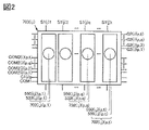
- FIG. 2 is a block diagram illustrating the configuration of the display device according to the embodiment.
- FIG. 3 is a block diagram illustrating the configuration of the display device according to the embodiment.
- FIG. 4 is a circuit diagram illustrating the configuration of the display device according to the embodiment.
- FIG. 5 is a timing chart for explaining the driving method of the display device according to the embodiment.
- FIG. 6 is a circuit diagram illustrating the configuration of the display device according to the embodiment.
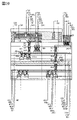
- FIG. 7 is a diagram for explaining the configuration of the display device according to the embodiment.
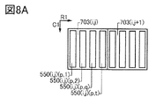
- 8A and 8B are block diagrams illustrating the configuration of the display device according to the embodiment.
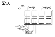
- 9A and 9B are block diagrams illustrating the configuration of the display device according to the embodiment.
- FIG. 10A and 10B are diagrams for explaining the configuration of the display device according to the embodiment.
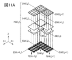
- 11A and 11B are diagrams for explaining the configuration of the display device according to the embodiment.
- 12A and 12B are diagrams for explaining the configuration of the display device according to the embodiment.
- 13A and 13B are diagrams for explaining the configuration of the display device according to the embodiment.
- 14A and 14B are diagrams for explaining the configuration of the display device according to the embodiment.
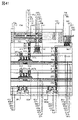
- FIG. 15 is a diagram for explaining the configuration of the display device according to the embodiment.
- FIG. 16 is a diagram for explaining the configuration of the display device according to the embodiment.
- 17A and 17B are diagrams for explaining the configuration of the display device according to the embodiment.
- FIG. 18 is a diagram illustrating the configuration of a display device according to an embodiment;
- FIG. 18 is a diagram illustrating the configuration of a display device according to an embodiment; FIG.
- FIG. 19 is a diagram for explaining the configuration of the display device according to the embodiment.
- 20A and 20B are diagrams for explaining the configuration of the display device according to the embodiment.
- FIG. 21 is a diagram for explaining the configuration of the display device according to the embodiment.
- FIG. 22 is a diagram for explaining the configuration of the display device according to the embodiment.
- 23A and 23B are diagrams for explaining the configuration of the display device according to the embodiment.
- FIG. 24 is a diagram illustrating the configuration of a display device according to an embodiment;
- FIG. 25 is a diagram for explaining the configuration of the display device according to the embodiment.
- 26A and 26B are diagrams for explaining the configuration of the display device according to the embodiment.
- FIG. 27 is a diagram illustrating the configuration of a display device according to an embodiment;
- FIG. 28 is a diagram illustrating the configuration of a display device according to an embodiment
- FIG. 29 is a diagram illustrating the configuration of a display device according to an embodiment
- FIG. 30 is a diagram for explaining the configuration of the display device according to the embodiment.
- FIG. 31 is a diagram illustrating the configuration of a display device according to an embodiment
- FIG. 32 is a diagram illustrating the configuration of a display device according to an embodiment
- 33A and 33B are diagrams for explaining the configuration of the display device according to the embodiment.
- FIG. 34 is a diagram illustrating the configuration of a display device according to an embodiment
- 35A and 35B are diagrams for explaining the configuration of the display device according to the embodiment.
- FIG. 36 is a diagram illustrating the configuration of a display device according to an embodiment;
- FIG. 36 is a diagram illustrating the configuration of a display device according to an embodiment; FIG.
- FIG. 37 is a diagram illustrating the configuration of a display device according to an embodiment
- FIG. 38 is a diagram illustrating the configuration of a display device according to an embodiment
- FIG. 39 is a diagram illustrating the configuration of a display device according to an embodiment
- FIG. 40 is a diagram for explaining the configuration of the display device according to the embodiment.
- FIG. 41 is a diagram illustrating the configuration of a display device according to an embodiment.
- 42A to 42C are diagrams for explaining the structure of a transistor according to an embodiment.
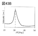
- 43A to 43C are diagrams illustrating metal oxides according to embodiments.
- 44A to 44D are diagrams illustrating electronic devices according to embodiments.
- 45A and 45B are diagrams for explaining the electronic device according to the embodiment.
- a display device of one embodiment of the present invention includes a first set of pixels, a second set of pixels, a first conductive film, and a second conductive film.
- the first set of pixels comprises a first set of light emitting devices, a first pad, a second pad, a conductive material and a first set of pixel circuitry.
- a first set of light emitting devices are electrically connected to the first pads, the first pads overlapping the second pads.
- a conductive material is sandwiched between the first pad and the second pad, the conductive material electrically connecting the first pad and the second pad.
- the second pads are electrically connected to the first set of pixel circuits.
- the first set of pixel circuits includes a first group of pixel circuits, and the first group of pixel circuits includes a first pixel circuit.
- the second set of pixels comprises a second set of light emitting devices and a second set of pixel circuits, the second set of light emitting devices in electrical communication with the second set of pixel circuits.
- the second set of pixel circuits includes a second set of pixel circuits, and the second set of pixel circuits includes a second pixel circuit.
- the first conductive film is electrically connected to the first group of pixel circuits and the second group of pixel circuits.
- the second conductive film is electrically connected to the first pixel circuit and the second pixel circuit.
- the first conductive film can be used to supply a signal to one or more pixel circuits included in the first set of pixel circuits during the first period. Also, during the same first time period, signals can be supplied to one or more pixel circuits in the second set of pixel circuits. Further, for example, signals can be supplied to a plurality of pixel circuits in the first period using the first conductive film.
- a second conductive film can be used to supply a signal to a first pixel circuit in a first set of pixel circuits during a second time period. Also, during the same second time period, the signal can be supplied to a second pixel circuit in the second set of pixel circuits. Also, during the second period, the first pixel circuit powers the second pads of the first set of pixels and the second pixel circuit powers the second pads of the second set of pixels. can power the
- the area of the second pads can be made close to the area occupied by the first set of pixel circuits.
- the area of the first pad can be made close to the area occupied by the first set of pixel circuits.
- the electrical connection between the second pad and the first pad is facilitated.
- electrical connection between the first set of pixel circuits and the first set of light emitting devices is facilitated.
- bonding of the first set of pixel circuits and the first set of light emitting devices is facilitated. As a result, it is possible to provide a novel display device with excellent convenience, usefulness, or reliability.
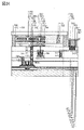
- FIG. 1A is a top view illustrating the structure of the display device of one embodiment of the present invention
- FIG. 1B is a cross-sectional view of the display device of one embodiment of the present invention illustrated in FIG. 1A taken along the line X1-X2.
- FIG. 2 is a block diagram illustrating the configuration of a set of pixels 703(i,j) shown in FIG. 1A.
- FIG. 3 is a block diagram illustrating the configuration of a set of pixels 703(i,j) shown in FIG.
- FIG. 4 is a circuit diagram illustrating the configuration of a set of pixels 703(i,j) shown in FIG.
- FIG. 5 is a timing chart illustrating the operation of the set of pixels 703(i,j) shown in FIG.
- FIG. 6 is a circuit diagram illustrating a configuration of a set of pixels 703(i,j) different from that in FIG.
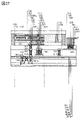
- FIG. 7 is a top view illustrating the structure of a display device of one embodiment of the present invention.
- FIG. 8A is a block diagram illustrating the configuration of the set of pixels 703(i,j) shown in FIG. 7, and FIG. 8B is a configuration different from the set of pixels 703(i,j) shown in FIG. 8A. It is a block diagram explaining.
- FIG. 9A is a block diagram illustrating the configuration of the set of pixels 703(i,j) shown in FIG. 8, and FIG. 9B is a configuration different from the set of pixels 703(i,j) shown in FIG. 9A. It is a block diagram explaining.
- a variable whose value is an integer of 1 or more may be used as a code.
- (p) which includes a variable p that takes an integer value of 1 or more, may be used as part of the code specifying one of the maximum p components.
- a display device 700 of one embodiment of the present invention has a set of pixels 703(i,j), a functional layer 520(1), and a functional layer 520(2) (see FIGS. 1A and 1B).
- the display device of one embodiment of the present invention can be formed by forming the functional layer 520(1) and the functional layer 520(2) and then bonding them together.
- a set of pixels 703(i, j) includes a set of light emitting devices 550(i,j), a set of pixel circuits 530(i,j), pads 541(i,j), pads 542(i,j). ) and conductive material 543(i,j) (see FIGS. 1B and 3).
- the set of light emitting devices 550(i,j) comprises light emitting devices 550(i,j)(p,1) through light emitting devices 550(i,j)(p,t) (FIGS. 2 and 3). reference).
- a light-emitting device that emits red light a light-emitting device that emits green light, and a light-emitting device that emits blue light can be used as a set of light-emitting devices.
- a set of pixel circuits 530(i,j) includes pixel circuits 530(i,j)(p,1) through pixel circuits 530(i,j)(p,t) (FIGS. 2 and 3). reference). Note that t is not limited to 3 and is an integer of 1 or more.
- a metal or composite material can be used for the conductive material 543 .
- nickel particles or gold-coated nickel particles can be used for the conductive material 543 .
- a composite material obtained by metal-plating resin can be used as the conductive material 543 .
- a composite material in which a metal or metal-plated resin is further coated with an insulating material can be used as the conductive material 543 .
- Functional layer 520(1) includes a set of pixel circuits 530(i,j) and pads 541(i,j). Pads 541(i,j) are electrically connected to a set of pixel circuits 530(i,j).
- Functional layer 520(2) overlaps functional layer 520(1), and functional layer 520(2) includes a set of light emitting devices 550(i,j) and pads 542(i,j). Pads 542(i,j) are electrically connected to a set of light emitting devices 550(i,j).
- the functional layer 520(2) includes a plurality of light emitting devices arranged in a matrix. Note that a light-emitting device that emits red light, a light-emitting device that emits green light, and a light-emitting device that emits blue light can be used for the functional layer 520(2).
- a plurality of light-emitting devices that emit blue light may be arranged in a matrix, and a color conversion layer that converts blue light into light of another color may be arranged directly above them.
- LED, OLED, etc. can be used for a light-emitting device.
- Conductive material 543(i,j) is sandwiched between pads 541(i,j) and pads 542(i,j) to electrically connect pads 541(i,j) and pads 542(i,j). do.
- conductive material 543(i,j) connects a set of pixel circuits 530(i,j) and a set of light emitting devices via pads 541(i,j) and pads 542(i,j). 550(i,j) are electrically connected.
- i, j) can be electrically connected.
- q pixel circuits can be connected to q light emitting devices using q pads or less. Note that q is an integer of 1 or more.
- three pixel circuits can be connected to three light emitting devices using a pair of pads. In addition, the number of connection points can be reduced, and the occurrence of poor connection can be suppressed.
- the area for connection can be made smaller than the area occupied by the set of light emitting devices 550(i, j).
- a plurality of actively driven pixel circuits are connected to a plurality of light-emitting devices using a pair of pads, thereby connecting the plurality of light-emitting devices. It becomes possible to drive like a passive drive. As a result, it is possible to provide a novel display device with excellent convenience, usefulness, or reliability.
- the display device of one embodiment of the present invention includes a conductive film COM1 and a conductive film COM2(i)(p, q) (see FIG. 3). Both the conductive film COM1 and the conductive film COM2(i)(p, q) function as wiring.
- a set of pixel circuits 530(i,j) includes pixel circuits 530(i,j)(p,q) and 530(i,j)(p,2) and a set of light emitting devices 550(i,j). ) includes light emitting devices 550(i,j)(p,q) and 550(i,j)(p,2). Also, the set of pixels 703(i,j) includes pixels 702(i,j)(p,q) (see FIG. 2). For example, the set of pixel circuits 530(i,j) comprises t pixel circuits. Note that t is an integer of 1 or more, and p is an integer of 1 or more and t or less.
- Pixel 702(i, j) (p, q) comprises pixel circuit 530(i,j)(p,q) and light emitting device 550(i,j)(p,q).
- the pixel circuits 530(i,j)(p,q) are electrically connected to the conductive film COM1, and the pixel circuits 530(i,j)(p,q) are connected to the light emitting device 550(i,q) for a predetermined period. j) electrically connected to one electrode of (p, q); For example, if the set of pixels 703(i,j) comprises pixels 702(i,j)(p,1) through 702(i,j)(p,t), then the set of pixels 703(i,j)(p,t) A period obtained by dividing the display period j) equally by t can be set as the predetermined period.
- the other electrode of the light emitting device 550(i,j)(p,q) is electrically connected to the conductive film COM2(i)(p,q), and the conductive film COM2(i)(p,q) During the period of , a predetermined voltage is supplied to the conductive film COM1. For example, the voltage that drives light emitting device 550(i,j)(p,q) at maximum brightness can be used for the predetermined voltage. Note that the pixel circuit 530(i,j)(p,q) controls the voltage distributed to the light emitting device 550(i,j)(p,q) from the predetermined voltage. In addition, during a period other than the predetermined period, a voltage is supplied to the conductive film COM2(i)(p,q) so that the light emitting device 550(i,j)(p,q) does not emit light.
- a light emitting device 550(i,j)(p,q) can be selected and the pixel circuit 530(i,j)(p,q) can be used to drive the light emitting device.
- pixel circuit 530(i,j)(p,q) can be selected to drive light emitting device 550(i,j)(p,q) for a predetermined period of time.
- a set of pixels 703(i,j) can be driven by dividing into multiple periods.
- the display device of one embodiment of the present invention includes a conductive film S1(j)q, a conductive film G1(i)p, and a conductive film G2(i)(p,q) (see FIG. 4).
- the conductive film S1(j)q, the conductive film S1(j)q ⁇ 1, the conductive film G1(i)p, and the conductive film G2(i)(p,q) all function as wirings.
- the pixel circuit 530(i,j)(p,q) includes a switch SW2(p,q), a switch SW11, a transistor M11, a capacitor C11 and a node N11.
- the switch SW11 has a first terminal electrically connected to the conductive film S1(j)q, a second terminal electrically connected to the node N11, and a potential of the conductive film G1(i)p. function to control the conducting state or the non-conducting state.
- the transistor M11 includes a gate electrode electrically connected to the node N11 and a first electrode electrically connected to the conductive film COM1.
- Capacitor C11 includes a conductive film electrically connected to node N11 and a conductive film electrically connected to conductive film COM1.
- the switch SW2(p,q) has a first terminal electrically connected to the second electrode of the transistor M11, a second terminal electrically connected to the pad 541(i,j), and a conducting terminal. It has a function of controlling the conducting state or the non-conducting state based on the potential of the film G2(i)(p,q).
- a set of pixel circuits 530(i,j) includes pixel circuits 530(i,j)(p,1) to pixel circuits 530(i,j)(p,t), and switch SW2(p,t). 1) to the switch SW2 (p, t), it is electrically connected to the pad 541 (i, j).
- the switches SW2(p,1) through SW2(p,t) select one of the pixel circuits 530(i,j)(p,1) through the pixel circuits 530(i,j)(p,t). and the pad 541 (i, j) to be electrically connected.
- the switches SW2(p, 1) to SW2(p, t) include the switch SW2(p, q+1).
- the illustrated circuit is an example of a circuit that can be used for the pixel circuit 530 (i, j) (p, q), and the configuration is not limited to this.
- the circuit shown in FIG. 6 can be used as part of the pixel circuit 530(i,j)(p,q).
- the switch SW12, the switch SW13, and the capacitor C12 can be used in the pixel circuit 530(i,j)(p,q).
- the display device also includes conductive films G12(i)p and G13(i)p electrically connected to the pixel circuits 530(i,j)(p,q).
- the switch SW12 has a first terminal electrically connected to the node N11, a second terminal electrically connected to the first electrode of the transistor M11, and the potential of the conductive film G12(i)p. , has a function of controlling the conducting state or the non-conducting state.
- the switch SW13 has a first terminal electrically connected to the node N11, a second terminal electrically connected to the conductive film COM1, and a conductive film G13(i)p based on the potentials of the conductive film G13(i)p. It has a function to control the non-conducting state.
- Capacitor C12 includes a conductive film connected to the second terminal of switch SW11 and a conductive film electrically connected to node N11.
- the display device of one embodiment of the present invention includes the driver circuit GD (see FIG. 1B).
- the drive circuit GD supplies the first selection signal to the conductive film G1(i)p.
- the pixel circuits 530(i,j)(p,1) to 530(i,j)(p,t) electrically connected to the conductive film G1(i)p are selected based on the first selection signal. For example, an image signal can be obtained from any one of the conductive films S1(j)1 to S1(j)t (see FIG. 3).
- the drive circuit GD also supplies the second selection signal to the conductive film G2(i)(p,q).
- the pixel circuit 530(i,j)(p,q) electrically connected to the conductive film G2(i)(p,q) is connected to the pad 541(i,j) based on the second selection signal. become conductive. Note that the drive circuit GD selects one of the conductive films G2(i)(p,1) to G2(i)(p,t) in a predetermined order, and applies the second selection signal for a predetermined period. supply.
- the drive circuit GD controls the potential of the conductive film COM2(i)(p, q). During the period of supplying the second selection signal to the conductive film G2(i)(p,q), the conductive film COM2(i)(p,q) is applied with a predetermined voltage between it and the conductive film COM1. Control the potential. For example, the potential of the conductive film COM2(i)(p,q) is controlled so as to apply a voltage that drives the light emitting device 550(i,j)(p,q) with maximum luminance.
- the drive circuit GD selects one of the conductive films COM2(i)(p,1) to COM2(i)(p,t) in a predetermined order and applies the predetermined voltage for a predetermined period. to control the potential.
- the potentials of the conductive films COM2(i)(p,1) to COM2(i)(p,t) are controlled to potentials that do not cause the light emitting device to emit light during periods other than the predetermined period.
- the display device of one embodiment of the present invention also includes pads 541(i)(p,q), pads 542(i)(p,q), and conductive materials 543(i)(p,q) (FIG. 1B). reference).
- the pads 541(i)(p,q) are electrically connected to, for example, the drive circuit GD, and the pads 542(i)(p,q) are connected to, for example, the conductive films COM2(i)(p,q). electrically connected.
- Conductive material 543(i)(p,q) is also sandwiched between pads 541(i)(p,q) and pads 542(i)(p,q) to provide pad 541(i)(p,q). q) and pads 542(i)(p,q) are electrically connected.
- the potential of the conductive film COM2(i)(p, q) can be controlled using the driving circuit GD.
- Pixel circuits 530(i,j)(p,1) to pixel circuits 530(i,j)(p,t) included in a set of pixel circuits 530(i,j) are selected based on the first selection signal. , to acquire the image signal.
- the pixel circuit 530(i,j)(p,q) acquires an image signal from the conductive film S1(j)q.
- one of the conductive films G2(i)(p,1) to G2(i)(p,t) is selected in a predetermined order, and the second selection signal is generated. supply. Further, one of the conductive films COM2(i)(p,1) to COM2(i)(p,t) is selected in a predetermined order, and a predetermined potential is supplied. Note that the conductive films G2(i)(p,1) to G2(i)(p,t) include the conductive film G2(i)(p+1,1).
- the pixel circuits 530(i,j)(p,1) to 530(i,j)(p,t) included in the set of pixel circuits 530(i,j) receive the acquired image signal and the second The potential of the pad 541 (i, j) is controlled based on the selection signal of .
- the pixel circuit 530 (i, j) (p, q ⁇ 1) is supplied with the second selection signal from the conductive film G2(i) (p, q ⁇ 1) during the period from time t14 to time t15,
- the potential of the pad 541 (i, j) is controlled based on the acquired image signal.
- the conductive film COM2(i)(p, q ⁇ 1) is supplied with a predetermined potential during the period from time t14 to time t15.
- the light-emitting device 550(i,j)(p,q-1) maintains the pad 541(i,j) and the conductive film COM2(i)(p,q-1) during the period from time t14 to time t15. Display is performed with a predetermined luminance based on the potential difference between them.
- the pixel circuit 530 (i, j) (p, q) is supplied with a selection signal from the conductive film G2 (i) (p, q) during the period from time t15 to time t16, and based on the acquired image signal. to control the potential of the pad 541(i,j). Further, the conductive film COM2(i)(p,q) is supplied with a predetermined potential during the period from time t15 to time t16.
- the light-emitting device 550(i,j)(p,q) is exposed to the potential difference between the pad 541(i,j) and the conductive film COM2(i)(p,q) during the period from time t15 to time t16. Based on this, display is performed with a predetermined brightness.
- the pixel circuit 530 (i, j) p+1 is supplied with the selection signal from the conductive film G2 (i) (p, q+1) during the period from time t16 to time t17, and the pad 541 Control the potential of (i,j).
- the conductive film COM2(i)(p, q+1) is supplied with a predetermined potential during the period from time t16 to time t17.
- the light-emitting device 550(i,j)(p,q+1) is exposed to the potential difference between the pad 541(i,j) and the conductive film COM2(i)(p,q+1) during the period from time t16 to time t17. Based on this, display is performed with a predetermined brightness.
- the switches SW2(p,1) to SW2(p,t) are connected to the conductive films G2(i)(p,1) to G2(i)(p,t). to a non-conducting state.
- the light emitting devices 550 (i, j) (p, 1) to the light emitting devices 550 (i, j) ( p, t) are supplied with a potential that causes them to be in a non-light-emitting state.
- period FR1 in the figure corresponds to one frame period. Accordingly, the display device of one embodiment of the present invention can be duty-driven.
- Driving method example 2 is different from driving method 1 in that display is divided into a plurality of times during one frame period from time t30 to time t40.
- driving method example 2 is different from driving method 1 in that display is divided into a plurality of times during one frame period from time t30 to time t40.
- Pixel circuits 530(i,j)(p,1) to pixel circuits 530(i,j)(p,t) included in a set of pixel circuits 530(i,j) are selected based on the first selection signal. , to acquire the image signal.
- the pixel circuits 530(i,j)(p,1) to 530(i,j)(p,t) included in the set of pixel circuits 530(i,j) receive the acquired image signal and the second The potential of the pad 541 (i, j) is controlled based on the selection signal of .
- the pixel circuits 530(i,j)(p,1) to 530(i,j)(p,t) included in the set of pixel circuits 530(i,j) receive the acquired image signal and the second The potential of the pad 541 (i, j) is controlled based on the selection signal of .
- period FR2 in the figure corresponds to one frame period. Accordingly, each pixel of the display device of one embodiment of the present invention can be displayed twice in one frame period. In addition, for example, it is possible to suppress the development of the color breaking phenomenon.
- the display device of one embodiment of the present invention also includes a functional layer 520(3) (see FIG. 1B).
- Functional layer 520(3) has a region sandwiching functional layer 520(1) with functional layer 520(2).
- functional layer 520(3), functional layer 520(1) and functional layer 520(2) are stacked.
- the functional layer 520(3) includes a driving circuit SD, and the driving circuit SD supplies image signals to the conductive films S1(j)q.
- Functional layer 520(3) also includes terminal 519B.
- an image signal to be displayed on the display device can be generated without increasing the outer size of the display device.
- the driving circuit SD and a set of pixel circuits 530(i, j) arranged directly above it can be electrically connected. As a result, it is possible to provide a novel display device with excellent convenience, usefulness, or reliability.
- the display device of one embodiment of the present invention includes the region 231 (see FIG. 7).
- Region 231 includes a group of pixels 703(i,1) through 703(i,n) and another group of pixels 703(1,j) through 703(m). , j).
- region 231 includes a group of pixel circuits 530(i,1) through 530(i,n) and another group of pixel circuits 530(1,j) through 530(i,n).
- a set of pixel circuits 530(m,j) is provided.
- m is an integer of 1 or more
- i is an integer of 1 or more and m or less.
- n is an integer of 1 or more
- j is an integer of 1 or more and n or less.
- a group of pixel circuits 530(i,1) to a group of pixel circuits 530(i,n) are arranged in the row direction (the direction indicated by arrow R1 in the figure).
- the (i,1) to set of pixel circuits 530(i,n) includes the set of pixel circuits 530(i,j) and the group of pixel circuits 530(i,1) to the set of pixels Circuit 530(i,n) is electrically connected to conductive film G1(i)p.
- Another group of pixel circuits 530 (1, j) to 530 (m, j) are arranged in the column direction (direction indicated by arrow C1 in the figure) intersecting the row direction,
- Another set of pixel circuits 530(1,j) through 530(m,j) includes a set of pixel circuits 530(i,j).
- Another group of pixel circuits 530(1,j) to 530(m,j) is electrically connected to the conductive film S1(j)q.
- the set of light-emitting devices 550(i,j) includes light-emitting devices 550(i,j)(p,1) to light-emitting devices 550(i,j)(p, t) (see FIG. 8A). Note that the light emitting devices 550(i,j)(p,1) to 550(i,j)(p,t) are arranged in the row direction.
- the set of light-emitting devices 550(i,j) includes light-emitting devices 550(i,j)(p,1) to light-emitting devices 550(i,j)(p,t). ), and the light emitting devices 550(i,j)(p,1) through 550(i,j)(p,t) may be arranged in columns (see FIG. 8B).
- the set of light-emitting devices 550(i,j) includes light-emitting devices 550(i,j)(p,1) to light-emitting devices 550(i,j)(p,t). ), and the light emitting devices 550(i,j)(p,1) through 550(i,j)(p,t) may be arranged in a matrix (see FIGS. 9A and 9B).
- FIG. 10A is a perspective view illustrating the structure of the display device of one embodiment of the present invention
- FIG. 10B is a top view illustrating part of the display device of one embodiment of the present invention shown in FIG. 10A.
- FIG. 11A is a perspective view illustrating the structure of the display device of one embodiment of the present invention
- FIG. 11B is a top view illustrating part of the display device of one embodiment of the present invention shown in FIG. 11A.
- FIG. 12A is a perspective view illustrating the structure of the display device of one embodiment of the present invention
- FIG. 12B is a top view illustrating part of the display device of one embodiment of the present invention shown in FIG. 12A.
- FIG. 13A is a top view illustrating the structure of the display device of one embodiment of the present invention
- FIG. 13B is a top view illustrating the structure of the display device of one embodiment of the present invention, which is different from the structure shown in FIG. 13A. is.
- FIG. 14A is a circuit diagram illustrating a pixel circuit that can be applied to the display device of one embodiment of the present invention
- FIG. 14B is a timing chart illustrating operation of the pixel circuit illustrated in FIG. 14A.
- FIG. 15 is a perspective view illustrating a structure of a set of pixels that can be applied to a display device of one embodiment of the present invention.
- FIG. 16 is a perspective view illustrating a configuration of a set of pixels that is different from the configuration shown in FIG. 15.
- FIG. 16 is a perspective view illustrating a configuration of a set of pixels that is different from the configuration shown in FIG. 15.
- FIG. 17A is a circuit diagram illustrating a pixel circuit that can be applied to the display device of one embodiment of the present invention
- FIG. 17B is a timing chart illustrating operation of the pixel circuit illustrated in FIG. 17A.
- FIG. 18 is a perspective view illustrating a structure of a set of pixels applicable to a display device of one embodiment of the present invention.
- FIG. 19 is a perspective view illustrating a configuration of a set of pixels that is different from the configuration shown in FIG. 18.
- FIG. 19 is a perspective view illustrating a configuration of a set of pixels that is different from the configuration shown in FIG. 18.
- FIG. 20A is a circuit diagram illustrating a pixel circuit that can be applied to the display device of one embodiment of the present invention
- FIG. 20B is a timing chart illustrating operation of the pixel circuit illustrated in FIG. 20A.
- FIG. 21 is a perspective view illustrating a structure of a set of pixels applicable to a display device of one embodiment of the present invention.
- FIG. 22 is a perspective view illustrating a configuration of a set of pixels that is different from the configuration shown in FIG. 21.
- FIG. 22 is a perspective view illustrating a configuration of a set of pixels that is different from the configuration shown in FIG. 21.
- FIG. 23A is a circuit diagram illustrating a pixel circuit that can be applied to the display device of one embodiment of the present invention
- FIG. 23B is a timing chart illustrating operation of the pixel circuit illustrated in FIG. 23A.
- FIG. 24 is a perspective view illustrating a structure of a set of pixels applicable to a display device of one embodiment of the present invention.
- FIG. 25 is a perspective view illustrating a configuration of a set of pixels that is different from the configuration shown in FIG. 24.
- FIG. 25 is a perspective view illustrating a configuration of a set of pixels that is different from the configuration shown in FIG. 24.
- FIG. 26A is a circuit diagram illustrating a pixel circuit that can be applied to the display device of one embodiment of the present invention
- FIG. 26B is a timing chart illustrating operation of the pixel circuit illustrated in FIG. 26A.
- FIG. 27 is a perspective view illustrating a structure of a set of pixels that can be applied to a display device of one embodiment of the present invention.
- FIG. 28 is a perspective view illustrating a configuration of a set of pixels that is different from the configuration shown in FIG. 27.
- FIG. 28 is a perspective view illustrating a configuration of a set of pixels that is different from the configuration shown in FIG. 27.
- FIG. 29 is a perspective view illustrating a configuration of a set of pixels that is different from the configurations shown in FIGS. 27 and 28.
- FIG. 29 is a perspective view illustrating a configuration of a set of pixels that is different from the configurations shown in FIGS. 27 and 28.
- the display device described in this embodiment includes a set of pixels 703 (i, j), a set of pixels 703 (i, j+1), a set of pixels 703 (i+1, j), and a conductive film G1. (i)p and a conductive film G2(i)(p,q) (see FIG. 10A).
- a set of pixels 703(i,j) comprises a set of light emitting devices 550(i,j), pads 542(i,j), pads 541(i,j), conductive materials 543(i,j) and one
- a set of pixel circuits 530(i,j) is provided.
- a set of light emitting devices 550(i,j) are electrically connected to pads 542(i,j).
- Pads 542(i,j) overlap pads 541(i,j), and pads 541(i,j) are electrically connected to a set of pixel circuits 530(i,j).
- conductive material 543(i,j) is sandwiched between pad 542(i,j) and pad 541(i,j), and conductive material 543(i,j) is sandwiched between pad 542(i,j) and pad 542(i,j). 541(i,j) are electrically connected.
- a set of pixel circuits 530(i,j) includes a group of pixel circuits 530(i,j)(p,1) through 530(i,j)(p,t), and a group of pixel circuits 530( i,j)(p,1) to pixel circuit 530(i,j)(p,t) includes pixel circuit 530(i,j)(p,q) (see FIG. 10B).
- the set of pixel circuits 530(i,j) includes a group of pixel circuits 530(i,j)(1,q) through 530(i,j)(s,q) to a group of pixel circuits.
- Pixel circuits 530(i,j)(1,q) through pixel circuits 530(i,j)(s,q) include pixel circuits 530(i,j)(p,q). Note that s is an integer of 1 or more.
- the set of pixel circuits 530(i,j) includes pixel circuits 530(i,j)(1,1) through pixel circuits 530(i,j)(s,t).
- the set of pixels 703(i,j+1) comprises a set of light emitting devices 550(i,j+1) and a set of pixel circuits 530(i,j+1) such that the set of light emitting devices 550(i,j+1) are electrically connected to a set of pixel circuits 530 (i, j+1) (see FIG. 10A).
- a set of pixel circuits 530(i,j+1) includes a group of pixel circuits 530(i,j+1)(p,1) through 530(i,j+1)(p,t), and a group of pixel circuits 530( i,j+1)(p,1) to pixel circuit 530(i,j+1)(p,t) includes pixel circuit 530(i,j+1)(p,q) (see FIG. 10B).
- the set of pixel circuits 530(i,j+1) includes pixel circuits 530(i,j+1)(1,1) through pixel circuits 530(i,j+1)(s,t).
- the set of pixels 703(i+1,j) comprises a set of light emitting devices 550(i+1,j) and a set of pixel circuits 530(i+1,j), and a set of light emitting devices 550(i+1,j). are electrically connected to a set of pixel circuits 530 (i+1, j) (see FIG. 10A).
- a set of pixel circuits 530(i+1,j) includes a group of pixel circuits 530(i+1,j)(1,q) through 530(i+1,j)(s,q), and a group of pixel circuits 530( i+1,j)(1,q) to pixel circuit 530(i+1,j)(s,q) includes pixel circuit 530(i+1,j)(p,q) (see FIG. 10B).
- the set of pixel circuits 530(i+1,j) includes pixel circuits 530(i+1,j)(1,1) through pixel circuits 530(i+1,j)(s,t).
- the conductive film G1(i)p is a group of pixel circuits 530(i,j)(p,1) to 530(i,j)(p,t) and a group of pixel circuits 530(i,j+1)(p , 1) to the pixel circuit 530 (i, j+1) (p, t).
- Conductive film G2(i) (p, q) is electrically connected to pixel circuit 530(i,j)(p,q) and pixel circuit 530(i,j+1)(p,q).
- the conductive film G1(i)p can be used to supply a signal to one or more pixel circuits included in the set of pixel circuits 530(i,j) in the first period. can. Also, during the same first time period, signals can be supplied to one or more pixel circuits in another set of pixel circuits 530(i,j+1). Further, for example, a signal can be supplied to a plurality of pixel circuits in the first period using the conductive film G1(i)p.
- the conductive film G2(i)(p,q) is used to apply a signal in the second period to the pixel circuit 530(i,j) ( p, q). Also, during the same second period, signals can be supplied to pixel circuits 530(i,j+1)(p,q) included in another set of pixel circuits 530(i,j+1). Also, in the second period, pixel circuit 530(i,j)(p,q) supplies power to pad 541(i,j) and pixel circuit 530(i,j+1)(p,q) supplies power to pad 541(i,j). 541(i,j+1) can be powered.
- the area of the pad 541(i,j) can be made close to the area occupied by the set of pixel circuits 530(i,j). Also, the area of the pads 542(i,j) can be made closer to the area occupied by the set of pixel circuits 530(i,j). Also, electrical connection between pads 541(i,j) and 542(i,j) is facilitated. Also, the electrical connection between the set of pixel circuits 530(i,j) and the set of light emitting devices 550(i,j) is facilitated. Alternatively, bonding of a set of pixel circuits 530(i,j) and a set of light emitting devices 550(i,j) is facilitated. As a result, it is possible to provide a novel display device with excellent convenience, usefulness, or reliability.
- a set of pixel circuits 530(i,j) described in this embodiment is, for example, pixel circuits 530(i,j)(p,q) and pixel circuits 530(i,j)(p+1,q). provided (see FIGS. 15 and 16).
- the pixel circuit 530(i,j)(p,q) includes a switch SW11, a switch SW2(p,q), a transistor M11, a capacitor C11 and a node N11 (see FIGS. 14A and 17A).
- the switch SW11 has a first terminal electrically connected to the conductive film S1(j)q, a second terminal electrically connected to the node N11, and a potential of the conductive film G1(i)p. function to control the conducting state or the non-conducting state.
- the transistor M11 includes a gate electrode electrically connected to the node N11 and a first electrode electrically connected to the conductive film COM1.
- the capacitor C11 includes a conductive film electrically connected to the node N11 and a conductive film electrically connected to the conductive film COM1.
- the switch SW2(p,q) has a first terminal electrically connected to the second electrode of the transistor M11, a second terminal electrically connected to the pad 541(i,j), and a conducting terminal. It has a function of controlling the conducting state or the non-conducting state based on the potential of the film G2(i)(p,q).
- Example 1 of driving method of display device>> A method for driving a display device of one embodiment of the present invention will be described. Specifically, using the operations of the pixel circuits 530(i,j)(p,q) and the pixel circuits 530(i,j)(p+1,q) included in the set of pixels 703(i,j), A method of driving the display device will be described (see FIGS. 14B and 15). Note that the period FR1 in the figure corresponds to one frame period.
- the first selection signal is supplied to the conductive film G1(i)p.
- the first selection signal is supplied to the conductive film G1(i)p+1 during the period from time t10 to time t11.
- the pixel circuit 530(i,j)(p,q) acquires an image signal from the conductive film S1(j)q based on the first selection signal. Also, the pixel circuit 530(i,j)(p+1.q) acquires an image signal from the conductive film S1(j)q+1 based on the first selection signal.
- the second selection signal is supplied to the conductive film G2(i)(p,q). Also, a predetermined potential is supplied to the conductive film COM2(i)(p, q).
- the pixel circuit 530 (i, j) (p, q) controls the potential of the pad 541 (i, j) based on the acquired image signal and the second selection signal.
- the second selection signal is supplied to the conductive film G2(i)(p+1,q). Also, a predetermined potential is supplied to the conductive film COM2(i)(p+1, q).
- the pixel circuit 530 (i, j) (p+1, q) controls the potential of the pad 541 (i, j) based on the acquired image signal and the second selection signal.
- a set of pixel circuits 530 (i, j) described in this embodiment includes, for example, pixel circuits 530 (i, j) (p, q), pixel circuits 530 (i, j) (p, q+1), It includes pixel circuits 530(i,j)(p,q+2) and pixel circuits 530(i,j)(p,q+3) (see FIGS. 18 and 19).
- the display device includes a conductive film S1(j)q+2 and a conductive film S1(j)q+3.
- the set of light emitting devices 550(i,j) comprises light emitting device 550(i,j)(p,q+2) and light emitting device 550(i,j)(p,q+3).
- the display device also includes a conductive film COM2(j)(p, q+1), a conductive film COM2(j)(p, q+2), and a conductive film COM2(j)(p, q+3) (see FIG. 19).
- ⁇ Driving Method Example 2 of Display Device>> A method for driving a display device of one embodiment of the present invention will be described. Specifically, using the operations of the pixel circuits 530 (i, j) (p, q) to 530 (i, j) (p, q+3) included in the set of pixels 703 (i, j), A method of driving the display device will be described (see FIGS. 17B and 18). Note that the period FR1 in the figure corresponds to one frame period.
- the pixel circuit 530(i,j)(p,q) acquires an image signal from the conductive film S1(j)q based on the first selection signal. Also, the pixel circuit 530(i,j)(p,q+1) acquires an image signal from the conductive film S1(j)q+1 based on the first selection signal.
- one of the conductive films G2(i)(p, q) to G2(i)(p, q+3) is selected in a predetermined order, and the second selection signal is generated. supply.
- one of the conductive films COM2(i)(p, q) to COM2(i)(p, q+3) is selected in a predetermined order, and a predetermined potential is supplied.
- the conductive films G2(i)(p,q) to G2(i)(p,q+3) include the conductive film G2(i)(p,q+2) and the conductive film COM2(i)(p,q).
- ) to the conductive film COM2(i)(p, q+3) include the conductive film COM2(i)(p, q+2).
- the pixel circuit 530(i,j)(p,q) is supplied with the second selection signal from the conductive film G2(i)(p,q) during the period from time t11 to time t12, and the acquired image is Based on the signal, the potential of the pad 541 (i, j) is controlled.
- the conductive film COM2(i)(p,q) is supplied with a predetermined potential during the period from time t11 to time t12.
- the light-emitting device 550(i,j)(p,q) is exposed to the potential difference between the pad 541(i,j) and the conductive film COM2(i)(p,q) during the period from time t11 to time t12. Based on this, display is performed with a predetermined brightness.
- the pixel circuit 530 (i, j) (p, q+1) is supplied with the second selection signal from the conductive film G2 (i) (p, q+1) during the period from time t12 to time t13, and the acquired image is Based on the signal, the potential of the pad 541 (i, j) is controlled.
- the conductive film COM2(i)(p, q+1) is supplied with a predetermined potential during the period from time t12 to time t13.
- the light-emitting device 550 (i, j) (p, q+1) is exposed to the potential difference between the pad 541 (i, j) and the conductive film COM2 (i) (p, q+1) during the period from time t12 to time t13. Based on this, display is performed with a predetermined brightness.
- the display device described in this embodiment is different from Structure Example 1 of the display device in that it includes the conductive film G2(j)(p, q) instead of the conductive film G2(i)(p, q). are different (see FIG. 11B).
- the different parts will be described in detail, and the above description will be used for the parts where the same configuration can be used.
- Conductive film G2(j)(p,q) is electrically connected to pixel circuit 530(i,j)(p,q) and pixel circuit 530(i+1,j)(p,q).
- signals are included in the set of pixel circuits 530(i,j) and the set of pixel circuits 530(i,j+1) in the first period. It can supply one or more pixel circuits. Further, for example, using the conductive film G1(i+1)p, a signal is supplied to one or a plurality of pixel circuits included in the set of pixel circuits 530(i+1, j) in a period different from the first period. can do.
- the conductive film G2(j)(p,q) is used to apply a signal in the second period to the pixel circuit 530(i,j)( p, q).
- signals can be supplied to pixel circuits 530(i+1,j)(p,q) included in another set of pixel circuits 530(i+1,j).
- pixel circuit 530(i,j)(p,q) supplies power to pad 541(i,j)
- pixel circuit 530(i+1,j)(p,q) supplies power to pad 541(i,j).
- 541(i+1,j) can be powered.
- a set of pixel circuits 530 (i, j) described in this embodiment includes, for example, pixel circuits 530 (i, j) (p, q), pixel circuits 530 (i, j) (p, q+1), It includes pixel circuits 530(i,j)(p,q+2) and pixel circuits 530(i,j)(p,q+3) (see FIGS. 21 and 22).
- Example 3 of Display Device>> A method for driving a display device of one embodiment of the present invention will be described. Specifically, using the operations of the pixel circuits 530 (i, j) (p, q) to 530 (i, j) (p, q+3) included in the set of pixels 703 (i, j), A method of driving the display device will be described (see FIGS. 20B and 21). Note that the period FR1 in the figure corresponds to one frame period.
- the pixel circuit 530(i,j)(p,q) acquires an image signal from the conductive film S1(j)q based on the first selection signal. Also, the pixel circuit 530(i,j)(p,q+1) acquires an image signal from the conductive film S1(j)q+1 based on the first selection signal.
- the pixel circuit 530(i,j)(p,q) is supplied with the second selection signal from the conductive film G2(j)(p,q) during the period from time t11 to time t12, and the acquired image is Based on the signal, the potential of the pad 541 (i, j) is controlled.
- the conductive film COM2(i)(p,q) is supplied with a predetermined potential during the period from time t11 to time t12.
- the light-emitting device 550(i,j)(p,q) is exposed to the potential difference between the pad 541(i,j) and the conductive film COM2(i)(p,q) during the period from time t11 to time t12. Based on this, display is performed with a predetermined brightness.
- the pixel circuit 530 (i, j) (p, q+1) is supplied with the second selection signal from the conductive film G2 (j) (p, q+1) during the period from time t12 to time t13, and the acquired image is Based on the signal, the potential of the pad 541 (i, j) is controlled.
- the conductive film COM2(i)(p, q+1) is supplied with a predetermined potential during the period from time t12 to time t13.
- the light emitting device 550 (i, j) (p, q+1) is exposed to the potential difference between the pad 541 (i, j) and the conductive film COM2 (i) (p, q+1) during the period from time t12 to time t13. Based on this, display is performed with a predetermined brightness.
- a set of pixel circuits 530 (i, j) described in this embodiment includes, for example, pixel circuits 530 (i, j) (p, q) to pixel circuits 530 (i, j) (p, q+3) and Pixel circuits 530(i,j)(p+1,q) to pixel circuits 530(i,j)(p+1,q+3) are provided (see FIGS. 24 and 25).
- the first selection signal is supplied to the conductive film G1(i)p.
- the first selection signal is supplied to the conductive film G1(i)p+1 during the period from time t10 to time t11.
- the pixel circuit 530(i,j)(p,q) acquires an image signal from the conductive film S1(j)q based on the first selection signal. Also, the pixel circuit 530(i,j)(p,q+1) acquires an image signal from the conductive film S1(j)q+1 based on the first selection signal.
- the pixel circuit 530(i,j)(p,q) is supplied with the second selection signal from the conductive film G2(j)(p,q) during the period from time t11 to time t12, and the acquired image is Based on the signal, the potential of the pad 541 (i, j) is controlled.
- the conductive film COM2(i)(p,q) is supplied with a predetermined potential during the period from time t11 to time t12.
- the light-emitting device 550(i,j)(p,q) is exposed to the potential difference between the pad 541(i,j) and the conductive film COM2(i)(p,q) during the period from time t11 to time t12. Based on this, display is performed with a predetermined brightness.
- the pixel circuit 530 (i, j) (p, q+1) is supplied with the second selection signal from the conductive film G2 (j) (p, q+1) during the period from time t12 to time t13, and the acquired image is Based on the signal, the potential of the pad 541 (i, j) is controlled.
- the conductive film COM2(i)(p, q+1) is supplied with a predetermined potential during the period from time t12 to time t13.
- the light emitting device 550 (i, j) (p, q+1) is exposed to the potential difference between the pad 541 (i, j) and the conductive film COM2 (i) (p, q+1) during the period from time t12 to time t13. Based on this, display is performed with a predetermined brightness.
- the pixel circuit 530 (i, j) (p+1, q) is supplied with the second selection signal from the conductive film G2 (j) (p+1, q) during the period from time t15 to time t16, and the acquired image is Based on the signal, the potential of the pad 541 (i, j) is controlled.
- the conductive film COM2(i)(p+1, q) is supplied with a predetermined potential during the period from time t15 to time t16.
- the light-emitting device 550(i,j)(p+1,q) is exposed to the potential difference between the pad 541(i,j) and the conductive film COM2(i)(p+1,q) during the period from time t15 to time t16. Based on this, display is performed with a predetermined brightness.
- the display device described in this embodiment mode has a conductive film G3(i)p and a conductive film G3(j)q instead of the conductive film G2(i)(p,q).
- This is different from configuration example 1 (see FIG. 12B).
- the different parts will be described in detail, and the above description will be used for the parts where the same configuration can be used.
- Conductive film G3(j)q is electrically connected to pixel circuit 530(i,j)(p,q) and pixel circuit 530(i+1,j)(p,q).
- the conductive film G1(i)p can be used to supply a signal to one or more pixel circuits included in the set of pixel circuits 530(i,j) in the first period. can. Also, during the same first time period, signals can be supplied to one or more pixel circuits in another set of pixel circuits 530(i,j+1). Further, for example, a signal can be supplied to a plurality of pixel circuits in the first period using the conductive film G1(i)p.
- the conductive film G3(i)p and the conductive film G3(j)q are used to apply a signal in the second period to the pixel circuit 530(i) included in the set of pixel circuits 530(i,j). , j) (p, q). Further, for example, the conductive film G3(i)p and the conductive film G3(j+1)q are used to apply a signal in the second period to the pixel circuit 530(i) included in the set of pixel circuits 530(i, j+1). , j+1)(p,q).
- the conductive film G3(i+1)p and the conductive film G3(j)q are used to apply a signal in the second period to the pixel circuit 530(i+1) included in the set of pixel circuits 530(i+1, j). , j) (p, q).
- two conductive films that intersect with each other for example, the conductive film G3(i)p and the conductive film G3(j)q are used to select one from a set of pixel circuits 530(i,j) and transmit a signal. supply, the number of conductive films can be reduced. As a result, it is possible to provide a novel display device with excellent convenience, usefulness, or reliability.
- a set of pixel circuits 530(i,j) described in this embodiment includes, for example, pixel circuits 530(i,j)(p,q) to pixel circuits 530(i,j)(p,q+3) and pixel Circuits 530(i,j)(p+1,q) to pixel circuits 530(i,j)(p+1,q+3) are provided (see FIGS. 27, 28 and 29).
- the pixel circuit 530 (i, j) differs from the configuration example 1 in that the switch SW2 (p, q) is replaced with a switch SW3p and a switch SW3q (see FIG. 26A).
- the different parts will be described in detail, and the above description will be used for the parts where the same configuration can be used.
- the switch SW3p has a first terminal electrically connected to the second electrode of the transistor M11, and has a function of controlling a conducting state or a non-conducting state based on the potential of the conductive film G3(i)p. .
- the switch SW3q has a first terminal electrically connected to the second terminal of the switch SW3p, a second terminal electrically connected to the pad 541(i, j), and a conductive film G3(j). It has a function of controlling the conducting state or the non-conducting state based on the potential of q.
- Example 5 for Display Device>> A method for driving a display device of one embodiment of the present invention will be described. Specifically, using the operations of the pixel circuits 530 (i, j) (p, q) to 530 (i, j) (p+1, q+3) included in the set of pixels 703 (i, j), A method of driving the display device will be described (see FIGS. 26B and 27). Note that the period FR1 in the figure corresponds to one frame period.
- the first selection signal is supplied to the conductive film G1(i)p.
- the first selection signal is supplied to the conductive film G1(i)p+1 during the period from time t10 to time t11.
- the pixel circuit 530(i,j)(p,q) acquires an image signal from the conductive film S1(j)q based on the first selection signal. Also, the pixel circuit 530(i,j)(p,q+1) acquires an image signal from the conductive film S1(j)q+1 based on the first selection signal.
- one of the conductive films G3(j)q to G3(j)q+3 is selected from the conductive films G3(j)q to G3(j)q+3 while supplying the third selection signal to the conductive film G3(i)p. It chooses in turn to provide a fourth selection signal. Also, one of the conductive films COM2(i)(p, q) to COM2(i)(p, q+3) is selected in a predetermined order, and a predetermined potential is supplied.
- the pixel circuit 530(i,j)(p,q) is supplied with the third selection signal from the conductive film G3(i)p during the period from time t11 to time t15. Further, during the period from time t11 to time t12, the fourth selection signal is supplied from the conductive film G3(j)q, and the potential of the pad 541(i,j) is controlled based on the acquired image signal.
- the conductive film COM2(i)(p,q) is supplied with a predetermined potential during the period from time t11 to time t12.
- the light-emitting device 550(i,j)(p,q) is exposed to the potential difference between the pad 541(i,j) and the conductive film COM2(i)(p,q) during the period from time t11 to time t12. Based on this, display is performed with a predetermined brightness.
- the pixel circuit 530(i,j)(p,q+1) is supplied with the third selection signal from the conductive film G3(i)p during the period from time t11 to time t15. Further, the fourth selection signal is supplied from the conductive film G3(j)q+1 during the period from time t12 to time t13, and the potential of the pad 541(i,j) is controlled based on the acquired image signal.
- the conductive film COM2(i)(p, q+1) is supplied with a predetermined potential during the period from time t12 to time t13.
- the light-emitting device 550 (i, j) (p, q+1) is exposed to the potential difference between the pad 541 (i, j) and the conductive film COM2 (i) (p, q+1) during the period from time t12 to time t13. Based on this, display is performed with a predetermined brightness.
- the pixel circuit 530(i,j)(p+1,q) is supplied with the third selection signal from the conductive film G3(i)p+1 during the period from time t15 to time t19. Further, during the period from time t15 to time t16, the fourth selection signal is supplied from the conductive film G3(j)q, and the potential of the pad 541(i,j) is controlled based on the acquired image signal.
- the conductive film COM2(i)(p+1, q) is supplied with a predetermined potential during the period from time t15 to time t16.
- the light-emitting device 550(i,j)(p+1,q) is exposed to the potential difference between the pad 541(i,j) and the conductive film COM2(i)(p+1,q) during the period from time t15 to time t16. Based on this, display is performed with a predetermined brightness.
- a display device of one embodiment of the present invention includes a conductive film COM2(i)(p, q) (see FIG. 13A). It also has a conductive film COM2(i+1)(p,q) and a conductive film COM2(j+1)(p,q).
- the set of light emitting devices 550(i,j) includes light emitting devices 550(i,j)(p,q). Also, the set of light emitting devices 550(i,j) includes light emitting devices 550(i,j)(1,1) through light emitting devices 550(i,j)(s,t).
- the display device or the light-emitting device in this embodiment has a function of displaying images using light-emitting diodes. Since the light-emitting diode is a self-luminous device, when the light-emitting diode is used as the display device, the display device does not require a backlight and does not need to be provided with a polarizing plate. Therefore, the power consumption of the display device can be reduced, and the display device can be made thinner and lighter.
- a display device using a light emitting diode as a display device can increase the luminance (for example, 5000 cd/m 2 or more, preferably 10000 cd/m 2 or more), and has a high contrast and a wide viewing angle. , a high display quality can be obtained.
- an inorganic material for the light-emitting material the life of the display device can be extended and the reliability can be improved.
- a micro LED is used as a light emitting diode.
- a micro LED having a double heterojunction will be described.
- the light-emitting diode is not particularly limited, and for example, a micro-LED having a quantum well junction, an LED using a nano-column, or the like may be used.
- the area of the light emitting region of the light-emitting diode is preferably 1 mm 2 or less, more preferably 10000 ⁇ m 2 or less, more preferably 3000 ⁇ m 2 or less, and even more preferably 700 ⁇ m 2 or less.
- the area of the region is preferably 1 ⁇ m 2 or more, preferably 10 ⁇ m 2 or more, and more preferably 100 ⁇ m 2 or more.
- a light-emitting diode whose light emitting region has an area of 10000 ⁇ m 2 or less may be referred to as a micro LED or a micro light-emitting diode.
- the display device of this embodiment preferably includes a transistor having a channel formation region in the metal oxide layer.
- a transistor using a metal oxide can consume less power. Therefore, by combining with micro LEDs, a display device with extremely reduced power consumption can be realized.
- the display device of this embodiment preferably includes a transistor having a channel formation region over a semiconductor substrate (eg, a silicon substrate). This enables high-speed operation of the circuit.
- a semiconductor substrate eg, a silicon substrate.
- the display device of this embodiment preferably includes a stacked transistor having a channel formation region in a semiconductor substrate and a transistor having a channel formation region in a metal oxide layer.
- the circuit can operate at high speed, and the power consumption can be extremely reduced.
- the set of light emitting devices 550(i,j+1) includes light emitting devices 550(i,j+1)(p,q). Also, the set of light emitting devices 550(i,j+1) includes light emitting devices 550(i,j+1)(1,1) through light emitting devices 550(i,j+1)(s,t).
- a set of light emitting devices 550(i+1,j) includes light emitting devices 550(i+1,j)(p,q). Also, the set of light emitting devices 550(i+1,j) includes light emitting devices 550(i+1,j)(1,1) through light emitting devices 550(i+1,j)(s,t).
- the conductive film COM2(i)(p,q) is used to select the light emitting device 550(i,j)(p,q) included in the set of light emitting devices 550(i,j).
- a light emitting device 550(i,j+1)(p,q) in the set of light emitting devices 550(i,j+1) can be selected.
- the pad 542(i,j) supplies power to the light emitting device 550(i,j)(p,q)
- the pad 542(i,j+1) is connected to the light emitting device 550(i,j+1)(p,q). q) can be powered.
- the area of the pads 542(i,j) can approximate the area occupied by the set of light emitting devices 550(i,j). Also, electrical connection between pads 541(i,j) and 542(i,j) is facilitated. Also, the electrical connection between the set of pixel circuits 530(i,j) and the set of light emitting devices 550(i,j) is facilitated. Alternatively, bonding of a set of pixel circuits 530(i,j) and a set of light emitting devices 550(i,j) is facilitated. As a result, it is possible to provide a novel display device with excellent convenience, usefulness, or reliability.
- a set of light emitting devices 550 (i, j) described in this embodiment includes, for example, a plurality of light emitting devices including light emitting devices 550 (i, j) (p, q) (FIGS. 15, 18, 21, 24 and 27).
- the display device described in this embodiment is different from Structure Example 4 of the display device in that it includes the conductive film COM2(j)(p, q) instead of the conductive film COM2(i)(p, q). are different (see FIG. 13B).
- the different parts will be described in detail, and the above description will be used for the parts where the same configuration can be used.
- the conductive film COM2(j)(p,q) is used to select the light emitting device 550(i,j)(p,q) included in the set of light emitting devices 550(i,j).
- a light emitting device 550(i+1,j)(p,q) in the set of light emitting devices 550(i+1,j) can be selected.
- the pad 542 (i, j) supplies power to the light emitting device 550 (i, j) (p, q)
- the pad 542 (i+1, j) is connected to the light emitting device 550 (i+1, j) (p, q).
- q) can be powered.
- a set of light emitting devices 550 (i, j) described in this embodiment includes, for example, light emitting devices 550 (i, j) (p, q) and light emitting devices 550 (i, j) (p+1, q). (see Figures 16, 19, 22, 25 and 29). Note that the light emitting device 550(i,j)(p+1,q) is electrically connected to the conductive film COM2(j)(p+1,q).
- FIG. 30 is a block diagram illustrating the structure of a display device of one embodiment of the present invention.
- FIG. 31 is a block diagram illustrating the configuration of the display section shown in FIG. 30.
- FIG. 31 is a block diagram illustrating the configuration of the display section shown in FIG. 30.
- FIG. 32 is a block diagram illustrating the structure of a display device of one embodiment of the present invention.
- 33A and 33B are block diagrams illustrating the configuration of the pixel shown in FIG. 32.
- FIG. 33A and 33B are block diagrams illustrating the configuration of the pixel shown in FIG. 32.
- FIG. 34 is a block diagram illustrating the structure of a display device of one embodiment of the present invention.
- FIG. 35A is a flowchart relating to the correction method
- FIG. 35B is a schematic diagram explaining the correction method.
- FIG. 30 shows a block diagram for explaining each configuration of the display device 10. As shown in FIG.
- the display device has a drive circuit 40 , a functional circuit 50 and a display section 60 .
- the drive circuit 40 has, for example, a gate driver 41 and a source driver 42 .
- the gate driver 41 has a function of driving a plurality of gate lines GL for outputting signals to the pixel circuits 62R, 62G, 62B.
- the source driver 42 has a function of driving a plurality of source lines SL for outputting signals to the pixel circuits 62R, 62G, 62B.
- the drive circuit 40 supplies voltages for display by the pixel circuits 62R, 62G, and 62B to the pixel circuits 62R, 62G, and 62B via a plurality of wirings.
- the functional circuit 50 has a CPU 51, and the CPU 51 can be used for arithmetic processing of data.
- the CPU 51 also has a CPU core 53 .
- the CPU core 53 has a flip-flop 80 for temporarily holding data used for arithmetic processing.
- the flip-flop 80 has a plurality of scan flip-flops 81 , and each scan flip-flop 81 is electrically connected to a backup circuit 82 provided in the display section 60 .
- the flip-flop 80 inputs and outputs scan flip-flop data (backup data) to and from a backup circuit 82 .
- FIG. 31 illustrates a configuration in which a plurality of pixels 61 are arranged in a matrix in the display portion 60 .
- the pixel 61 has a backup circuit 82 in addition to pixel circuits 62R, 62G, and 62B.
- both the backup circuit 82 and the pixel circuits 62R, 62G, and 62B can be configured with OS transistors, and therefore can be arranged in the same pixel.
- the display unit 60 has a plurality of pixels 61 provided with pixel circuits 62R, 62G, 62B and a backup circuit .
- the backup circuit 82 does not necessarily have to be arranged in the pixel 61 which is the repeating unit, as described with reference to FIG. They can be freely arranged according to the shape of the display section 60, the shapes of the pixel circuits 62R, 62G, and 62B, and the like.
- FIG. 32 is a block diagram schematically showing a configuration example of the display device 10 which is a display device of one embodiment of the present invention.
- the display device 10 has a layer 20 and a layer 30 , and the layer 30 can be laminated above the layer 20 , for example. Between layers 20 and 30 there may be an interlayer insulator or a conductor for making electrical connections between the different layers.
- a transistor provided in the layer 20 can be, for example, a transistor including silicon in a channel formation region (also referred to as a Si transistor), for example, a transistor including single crystal silicon in a channel formation region.
- a transistor including single crystal silicon in a channel formation region is used as the transistor provided in the layer 20
- the on current of the transistor can be increased. Therefore, the circuit included in the layer 20 can be driven at high speed, which is preferable.
- the Si transistor can be formed by fine processing such that the channel length is 3 nm to 10 nm
- the display device 10 can be provided with an accelerator such as a CPU or GPU, an application processor, or the like.
- Layer 20 is provided with drive circuitry 40 and functional circuitry 50 .
- the Si transistors of layer 20 can increase the on-current of the transistors. Therefore, each circuit can be driven at high speed.
- the drive circuit 40 has a gate line drive circuit, a source line drive circuit, and the like for driving the pixel circuits 62R, 62G, and 62B.
- the drive circuit 40 has, for example, a gate line drive circuit and a source line drive circuit for driving the pixels 61 of the display section 60 .
- the drive circuit 40 includes an LVDS (Low Voltage Differential Signaling) circuit or a D/A (Digital to Analog) conversion circuit having a function as an interface for receiving data such as image data from the outside of the display device 10. may have.
- the Si transistors of layer 20 can increase the on-current of the transistors.
- the channel length or channel width of the Si transistor may be varied according to the operating speed of each circuit.
- a bottom-gate transistor, a top-gate transistor, or the like can be used as the transistor provided in the layer 30 .
- a semiconductor containing a Group 14 element can be used for the semiconductor film.
- a semiconductor containing silicon can be used for the semiconductor film.
- hydrogenated amorphous silicon, polysilicon, single crystal silicon can be used.
- a metal oxide can also be used for the semiconductor film.
- an OS transistor can be used.
- a transistor including an oxide containing at least one of indium, element M (element M is aluminum, gallium, yttrium, or tin), and zinc in a channel formation region is preferably used.
- Such an OS transistor has a very low off-state current. Therefore, it is preferable to use an OS transistor as a transistor provided in a pixel circuit included in a display portion, because analog data written to the pixel circuit can be retained for a long time.
- the layer 30 is provided with a display section 60 provided with a plurality of pixels 61 .
- the pixel 61 is provided with pixel circuits 62R, 62G, and 62B whose emission of red, green, and blue is controlled.
- Pixel circuits 62 R, 62 G, and 62 B have functions as sub-pixels of pixel 61 . Since the pixel circuits 62R, 62G, and 62B have OS transistors, analog data written to the pixel circuits can be retained for a long period of time.
- a backup circuit 82 is provided for each of the pixels 61 included in the layer 30 . Note that the backup circuit may be called a storage circuit or a memory circuit. Also, the backup circuit inputs/outputs data (backup data BD) of the scan flip-flops to/from the flip-flops 80 .
- FIG. 33A and 33B show a configuration example of the pixel circuit 62 applicable to the pixel circuits 62R, 62G, and 62B, and the light emitting element 70 connected to the pixel circuit 62.
- FIG. 33A is a diagram showing the connection of each element
- FIG. 33B is a diagram schematically showing the vertical relationship among the drive circuit 40, the pixel circuit 62, and the light emitting element 70.
- a display element can be replaced with “device” in some cases.
- a display element, a light-emitting element, and a liquid crystal element can be called a display device, a light-emitting device, and a liquid crystal device.
- a pixel circuit 62 shown as an example in FIGS. 33A and 33B includes a switch SW11, a switch SW2p, a switch SW12, a switch SWm, a transistor M11, and a capacitor C11.
- the switch SW11, the switch SW2p, the switch SW12, the switch SWm, and the transistor M11 can be composed of OS transistors.
- Each transistor of the switch SW11, the switch SW2p, the switch SW12, the switch SWm, and the transistor M11 preferably has a back gate electrode. It can be configured to give a different signal than the electrodes.
- the switch SW11 is in a conducting state or a non-conducting state based on the potentials of a first terminal electrically connected to the source line SL, a second terminal electrically connected to the node N11, and the gate line GL11. It has a function to control
- the transistor M11 includes a gate electrode electrically connected to the node N11 and a first electrode electrically connected to the conductive film COM1.
- the conductive film COM1 is a wiring for applying a potential for supplying a current to the light emitting element 70 and a wiring for outputting the current flowing through the pixel circuit 62 to the drive circuit 40 or the function circuit 50 .
- Capacitor C11 includes a conductive film electrically connected to node N11 and a conductive film electrically connected to conductive film COM1.
- the switch SW2p has a first terminal electrically connected to the second electrode of the transistor M11, a second terminal electrically connected to the first pad 541(i, j), and a gate line GL2p. It has a function of controlling a conducting state or a non-conducting state based on the potential of .
- the light emitting element 70 has one electrode electrically connected to the first pad 541(i, j), the other electrode electrically connected to the conductive film COM2(i)(p, q), Prepare.
- the conductive film COM2(i)(p,q) is a wiring for applying a potential for supplying current to the light emitting element 70 .
- the intensity of light emitted from the light emitting element 70 can be controlled according to the image signal applied to the gate electrode of the transistor M11.
- the switch SW12 has a first terminal electrically connected to the wiring V0, a second terminal electrically connected to the first electrode of the transistor M11, and the potential of the gate line GL12. It has a function to control the conducting state or the non-conducting state.
- the wiring V0 is a wiring for applying a reference potential and a wiring for outputting the current flowing through the pixel circuit 62 to the driving circuit 40 or the function circuit 50 .
- the switch SWm has a first terminal electrically connected to the wiring V1, a second terminal electrically connected to the first pad 541(i, j), and a conducting state or a non-conductive state based on a control signal. It has a function to control the non-conducting state.
- a wiring V1 is a wiring for applying a reference potential.
- a current value that can be used for setting pixel parameters can be output from the wiring V0 via the switches SWm and SW12. More specifically, the wiring V0 can function as a monitor line for outputting the current flowing through the transistor M11 to the outside.
- the current output to the wiring V0 is converted into a voltage by a source follower circuit or the like and output to the outside. Alternatively, it can be converted into a digital signal by an AD converter or the like and output to the drive circuit 40 or the like.
- the pixel density of the display device 10 can be 1000 ppi or more, or 5000 ppi or more, or 7000 ppi or more. Therefore, the display device 10 can be a display device for AR or VR, for example, and can be suitably applied to an electronic device such as an HMD in which the distance between the display unit and the user is short.
- the gate line GL11, the gate line GL12, the gate line GL2p, the conductive film COM1, the wiring V0, the wiring V1, and the source line SL are supplied from the driver circuit 40 below the pixel circuit 62 via wiring.
- wiring for supplying signals and voltages of the drive circuit 40 may be routed around the periphery of the display section 60 and electrically connected to the pixel circuits 62 arranged in a matrix on the layer 30 . In this case, it is effective to provide the gate driver 41 of the driving circuit 40 in the layer 30 . That is, it is effective to use an OS transistor as the transistor of the gate driver 41 .
- a configuration in which part of the function of the source driver 42 of the drive circuit 40 is provided in the layer 30 is effective. For example, it is effective to provide the layer 30 with a demultiplexer that distributes the signal output by the source driver 42 to each source line. It is effective to use an OS transistor as the transistor of the demultiplexer.
- the backup circuit 82 is preferably a memory having an OS transistor, for example.
- a backup circuit composed of an OS transistor can suppress a voltage drop according to the data to be backed up and consume almost no power to hold data because of the characteristics of the OS transistor that the off-state current is extremely small. , and other advantages.
- a backup circuit 82 having an OS transistor can be provided in the display portion 60 in which a plurality of pixels 61 are arranged. FIG. 32 illustrates how each pixel 61 is provided with a backup circuit 82 .
- a backup circuit 82 including an OS transistor can be stacked with the layer 20 including the Si transistor.
- the backup circuit 82 may be arranged in a matrix like the sub-pixels in the pixel 61, or may be arranged for every plurality of pixels. That is, the backup circuit 82 can be arranged in the layer 30 without being restricted by the arrangement of the pixels 61 . Therefore, it is possible to increase the degree of freedom of the display section/circuit layout, to arrange the circuit area without increasing the circuit area, and to increase the storage capacity of the backup circuit 82 required for arithmetic processing.
- FIG. 34 shows a modification of each configuration of the display device 10 described above.
- a block diagram of the display device 10A shown in FIG. 34 corresponds to a configuration in which an accelerator 52 is added to the functional circuit 50 in the display device 10 of FIG.
- the accelerator 52 functions as a dedicated arithmetic circuit for sum-of-products arithmetic processing of the artificial neural network NN. In the calculation using the accelerator 52, it is possible to perform processing such as correcting the contour of the image by up-converting the display data. It should be noted that power consumption can be reduced by controlling the power gating of the CPU 51 while the accelerator 52 is performing arithmetic processing.
- the display device of one embodiment of the present invention can be formed by stacking the pixel circuit and the functional circuit, a defective pixel can be detected using the functional circuit provided below the screen circuit. By using the defective pixel information, the display defect caused by the defective pixel can be corrected, and normal display can be performed.
- correction methods exemplified below may be performed by a circuit provided outside the display device. Also, part of the correction method may be performed by the drive circuit 40 of the display device 10 .
- FIG. 35A is a flow chart relating to the correction method described below.
- step S1 a correction operation is started in step S1.
- step S2 the pixel current is read.
- each pixel can be driven to output current to a monitor line electrically connected to the pixel.
- step S3 the read current is converted into voltage.
- a digital signal is to be handled in subsequent processing, it can be converted into digital data in step S3.
- ADC analog-to-digital conversion circuit
- Pixel parameters of each pixel are obtained based on the obtained data.
- Pixel parameters include, for example, the threshold voltage or field effect mobility of a driving transistor, the threshold voltage of a light emitting element, and the current value at a predetermined voltage.
- step S5 it is determined whether or not each pixel is abnormal based on the pixel parameters. For example, if the pixel parameter value exceeds (or falls below) a predetermined threshold value, the pixel is identified as an abnormal pixel.
- the abnormal pixel includes a dark point defect whose luminance is extremely low with respect to the input data potential, a bright point defect whose luminance is extremely high, and the like.
- step S5 the address of the abnormal pixel and the type of defect can be identified and obtained.
- step S6 correction processing is performed.
- FIG. 35B schematically shows 3 ⁇ 3 pixels.
- the center pixel is pixel 61D which is a dark spot defect.
- FIG. 35B schematically shows that the pixel 61D is turned off and the surrounding pixels 61N are turned on with a predetermined luminance.
- a dark spot defect is a defect in which the luminance of a pixel is unlikely to reach the normal luminance even if correction is performed to increase the data potential to be input to the pixel. Therefore, as shown in FIG. 35B, correction is performed to increase the brightness of the pixels 61N surrounding the dark spot defect pixel 61D. As a result, a normal image can be displayed even when a dark spot defect occurs.
- the bright spot defect can be made inconspicuous by lowering the brightness of the surrounding pixels.
- correction parameters can be set for each pixel.
- corrected image data for displaying an optimum image on the display device 10 can be generated.
- correction parameters can be set so as to cancel (level) variations in pixel parameters.
- a reference value is set based on the median value or average value of pixel parameters for some or all pixels, and the correction value for canceling the difference from the reference value for the pixel parameter of a predetermined pixel is It can be set as a correction parameter for the pixel.
- correction data that considers both a correction amount for compensating for the abnormal pixel and a correction amount for canceling variations in pixel parameters.
- step S7 the correction operation is terminated.
- an image can be displayed based on the correction parameters acquired in the correction operation and the input image data.
- a neural network may be used as one of the correction operations.
- the configuration is such that sum-of-products computation is repeated.
- Computation using the accelerator 52 can correct the above-described display failure. It should be noted that power consumption can be reduced by controlling the power gating of the CPU 51 while the accelerator 52 is performing arithmetic processing.
- the neural network can determine correction parameters based on inference results obtained by machine learning, for example.
- DNN deep neural networks
- CNN convolutional neural networks
- RNN recurrent neural networks
- DBM deep Boltzmann machines
- DBN deep belief networks
- the above-described CPU 51 can continue to hold the data in the middle of the calculation as backup data. Therefore, it is particularly effective in performing a huge amount of arithmetic processing such as an arithmetic operation based on an artificial neural network.
- the CPU 51 function as an application processor, it is possible to reduce power consumption as well as reduce display defects by combining driving with variable frame frequency.
- FIG. 36 is a cross-sectional view illustrating the structure of a display device of one embodiment of the present invention.
- FIG. 37 is a cross-sectional view illustrating a structure of a display device of one embodiment of the present invention, which is different from the structure shown in FIG.
- FIG. 38 is a cross-sectional view illustrating a structure of a display device of one embodiment of the present invention, which is different from the structure shown in FIG.
- FIG. 39 is a cross-sectional view illustrating a structure of a display device of one embodiment of the present invention, which is different from the structure shown in FIG.
- FIG. 40 is a cross-sectional view illustrating a structure of a display device of one embodiment of the present invention, which is different from the structures illustrated in FIGS.
- FIG. 41 is a cross-sectional view illustrating a structure of a display device of one embodiment of the present invention, which is different from the structures illustrated in FIGS.
- FIG. 36 is a cross-sectional view showing a configuration example of the display device 10.
- the display device 10 has an insulator 421 and a substrate 705 , and the insulator 421 and the substrate 705 are attached with a sealant 712 .
- An OS transistor is preferably used for the pixel circuit.
- at least part of the driver circuit may be formed using an OS transistor.
- at least part of the functional circuit may be formed using an OS transistor.
- at least part of the drive circuit may be externally attached.
- at least part of the functional circuit may be externally attached.
- Insulator 421 As the insulator 421, various insulator substrates such as a glass substrate and a sapphire substrate can be used. An insulator 214 is provided over the insulator 421 and an insulator 216 is provided over the insulator 214 .
- Insulator 222 ⁇ Insulator 222, Insulator 224, Insulator 254, Insulator 280, Insulator 274, Insulator 281>>
- An insulator 222 , an insulator 224 , an insulator 254 , an insulator 280 , an insulator 274 , and an insulator 281 are provided over the insulator 216 .
- the insulator 421 , the insulator 214 , the insulator 280 , the insulator 274 , and the insulator 281 function as interlayer films and function as planarization films that cover the uneven shapes below them. good too.
- An insulator 361 is provided over the insulator 281 .
- a conductor 317 and a conductor 337 are embedded in the insulator 361 .
- the height of the top surface of the conductor 337 and the height of the top surface of the insulator 361 can be made approximately the same.
- An insulator 363 is provided over the conductor 337 and the insulator 361 .
- a conductor 347 , a conductor 353 , a conductor 355 , and a conductor 357 are embedded in the insulator 363 .
- the height of the top surfaces of the conductors 353, 355, and 357 and the height of the top surface of the insulator 363 can be approximately the same.
- a conductor 341 , a conductor 343 , and a conductor 351 are embedded in the insulator 363 .
- the height of the top surface of the conductor 351 and the height of the top surface of the insulator 363 can be made approximately the same.
- the insulator 361 and the insulator 363 function as interlayer films and may function as planarization films that cover the uneven shapes below them.
- the top surface of the insulator 363 may be planarized by planarization treatment using a chemical mechanical polishing (CMP) method or the like in order to improve planarity.
- CMP chemical mechanical polishing
- connection electrode 760 is provided over the conductor 353 , the conductor 355 , the conductor 357 , and the insulator 363 .
- An anisotropic conductor 780 is provided to be electrically connected to the connection electrode 760
- an FPC (Flexible Printed Circuit) 716 is provided to be electrically connected to the anisotropic conductor 780 .
- Various signals and the like are supplied to the display device 10 from the outside of the display device 10 by the FPC 716 .
- FIG. 36 shows three conductors, the conductor 353, the conductor 355, and the conductor 357, as conductors having a function of electrically connecting the connection electrode 760 and the conductor 347;
- the mode is not limited to this.
- the number of conductors having a function of electrically connecting the connection electrode 760 and the conductor 347 may be one, two, or four or more. By providing a plurality of conductors having a function of electrically connecting the connection electrode 760 and the conductor 347, contact resistance can be reduced.
- a transistor 750 is provided over the insulator 214 .
- the transistor 750 can be the transistor provided in the layer 30 described in Embodiment 3.
- a transistor provided in the pixel circuit 62 can be used.
- An OS transistor can be preferably used as the transistor 750 .
- An OS transistor has a feature of extremely low off-state current. Therefore, since the retention time of image data or the like can be lengthened, the frequency of refresh operations can be reduced. Therefore, power consumption of the display device 10 can be reduced.
- the transistor 750 can be a transistor provided in the backup circuit 82 .
- An OS transistor can be preferably used as the transistor 750 .
- An OS transistor has a feature of extremely low off-state current. Therefore, data held in the flip-flop can be held even during a period in which sharing of the power supply voltage is stopped. Therefore, the normally-off operation of the CPU (the operation of intermittently stopping the power supply voltage) can be achieved. Therefore, power consumption of the display device 10 can be reduced.
- a conductor 301 a and a conductor 301 b are embedded in the insulator 254 , the insulator 280 , the insulator 274 , and the insulator 281 .
- Conductor 301 a is electrically connected to one of the source and drain of transistor 750
- conductor 301 b is electrically connected to the other of the source and drain of transistor 750 .
- the height of the top surfaces of the conductors 301a and 301b and the height of the top surface of the insulator 281 can be made approximately the same.
- a conductor 311 , a conductor 313 , a conductor 331 , a capacitor 790 , a conductor 333 , and a conductor 335 are embedded in the insulator 361 .
- the conductors 311 and 313 are electrically connected to the transistor 750 and function as wirings.
- the conductors 333 and 335 are electrically connected to the capacitor 790 .
- the height of the top surfaces of the conductors 331, 333, and 335 and the height of the top surface of the insulator 361 can be approximately the same.
- capacitor 790 has lower electrode 321 and upper electrode 325 .
- An insulator 323 is provided between the lower electrode 321 and the upper electrode 325 . That is, the capacitor 790 has a laminated structure in which the insulator 323 functioning as a dielectric is sandwiched between a pair of electrodes. Note that although FIG. 36 shows an example in which the capacitor 790 is provided over the insulator 281, the capacitor 790 may be provided over an insulator different from the insulator 281.
- FIG. 36 shows an example in which the conductor 301a, the conductor 301b, and the conductor 305 are formed in the same layer. Further, an example in which the conductor 311, the conductor 313, the conductor 317, and the lower electrode 321 are formed in the same layer is shown. Further, an example in which the conductor 331, the conductor 333, the conductor 335, and the conductor 337 are formed in the same layer is shown. Further, an example in which the conductor 341, the conductor 343, and the conductor 347 are formed in the same layer is shown. Furthermore, an example in which the conductor 351, the conductor 353, the conductor 355, and the conductor 357 are formed in the same layer is shown. By forming a plurality of conductors in the same layer, the manufacturing process of the display device 10 can be simplified, so that the manufacturing cost of the display device 10 can be reduced. Note that they may be formed in different layers and may have different types of materials.
- a display device 10 shown in FIG. 36 has a light emitting element 70 .
- the light-emitting element 70 has a conductor 772 , a light-emitting layer 786 , and a conductor 788 .
- the light-emitting layer 786 has an inorganic compound or an organic compound.
- a compound semiconductor can be used for the light emitting layer 786 .
- the light-emitting layer 786 can be sandwiched between the P-type clad layer and the N-type clad layer. This allows carriers to recombine in the light-emitting layer 786 . As a result, light emission accompanying recombination of carriers can be obtained.
- a layered material that emits blue light, a layered material that emits green light, a layered material that emits red light, or the like is used for the light-emitting layer 786 .
- a gallium-phosphide compound, a gallium-arsenide compound, a gallium-aluminum-arsenide compound, an aluminum-gallium-indium-phosphide compound, an indium-gallium nitride compound, or the like can be used for the light emitting layer 786 .
- quantum dots or the like can be used for the light-emitting layer 786 .
- a colloidal quantum dot material, an alloy quantum dot material, a core-shell quantum dot material, a core quantum dot material, or the like can be used for the light emitting layer 786 .
- a fluorescent organic compound, a phosphorescent organic compound, or the like can be used for the light-emitting layer 786 .
- a low-molecular-weight compound can be used for the light-emitting layer 786 .
- a polymer compound can be used for the light-emitting layer 786 .
- a mini-LED can be used for the light emitting element 70 .
- the light emitting element 70 uses a mini-LED whose light emitting region has an area of 1 mm 2 or less, preferably 50,000 ⁇ m 2 or less, more preferably 30,000 ⁇ m 2 or less, even more preferably 10,000 ⁇ m 2 or less, or 200 ⁇ m 2 or more. be able to.
- a micro LED can be used as the light emitting element 70 .
- the light-emitting element 70 uses a micro LED whose light emitting region has an area of less than 200 ⁇ m 2 , preferably 60 ⁇ m 2 or less, more preferably 15 ⁇ m 2 or less, even more preferably 5 ⁇ m 2 or less, or 3 ⁇ m 2 or more. be able to.
- a material that transmits visible light can be used for the conductors 772 and 788 .
- a light-transmitting material for example, an oxide material containing indium, zinc, tin, or the like is preferably used.
- the light-emitting element 70 has a bottom emission structure in which light is emitted to the conductor 772 side, a top emission structure in which light is emitted to the conductor 788 side, or light is emitted to both the conductor 772 side and the conductor 788 side.
- a dual emission structure may be used.
- a material that is reflective to visible light can also be used for conductor 772 or conductor 788 .
- a reflective material for example, a material containing aluminum, silver, or the like may be used.
- the light emitting device 70 can have a micro-optical resonator (microcavity) structure.
- a micro-optical resonator microcavity
- light of predetermined colors for example, RGB
- the display device 10 can perform color display.
- Absorption of light by the colored layer can be suppressed by adopting a structure in which the colored layer is not provided.
- the display device 10 can display a high-brightness image, and the power consumption of the display device 10 can be reduced.
- the light-emitting element 70 is connected to the source or drain of the transistor 750 through the conductor 772, the pad 542, the conductive material 543, the pad 541, the conductor 351, the conductor 341, the conductor 331, the conductor 313, and the conductor 301b. electrically connected to the other.
- conductor 772, pad 542, conductive material 543, pad 541, conductor 351, conductor 341, conductor 331, conductor 313, and conductor 301b electrically connect light emitting element 70 to the pixel circuit. It has the function to
- Pad 542 is formed in contact with conductor 772 .
- Conductive material 543 is dispersed in insulator 734, for example. This provides the function of an anisotropically conductive adhesive or an anisotropically conductive film.
- the pads 542 and 541 may be directly bonded using a surface activation bonding method, such as a metal-metal bonding method, specifically a copper-copper bonding method.
- the conductive film COM2p is formed in contact with the conductor 772 . Also, for example, a voltage is supplied to drive the light emitting element 70 with maximum luminance.
- the color conversion layer CC is provided so as to overlap with the light emitting element 70 . Also, the color conversion layer CC has a function of converting the color of the light emitted from the light emitting element 70 into another color.
- a material that converts blue light emitted from the light emitting element into green light can be used for the color conversion layer CC.
- a material that converts blue light into red light can be used for the color conversion layer CC.
- a material that converts ultraviolet light emitted from the light emitting element into blue light can be used for the color conversion layer CC.
- a material that converts ultraviolet light into green light can be used for the color conversion layer CC.
- a material that converts ultraviolet light into red light can be used for the color conversion layer CC.
- a plurality of light-emitting elements are formed in the same process using the same material, and the color conversion layers CC are separately formed using different materials by overlapping the respective light-emitting elements, thereby displaying colors different from each other. can be done.
- a colored layer can be provided.
- the colored layer is provided so as to have a region overlapping with the light emitting element 70 .
- the color purity of the light extracted from the light emitting element 70 can be increased. Thereby, a high-quality image can be displayed on the display device 10 .
- all the light emitting elements 70 of the display device 10 can be light emitting elements that emit white light.
- the display device 10 can be provided with optical members (optical substrates) such as a polarizing member, a retardation member, and an antireflection member.
- optical members optical substrates
- a polarizing member such as a polarizing member, a retardation member, and an antireflection member.
- An insulator 730 is provided over the insulator 363 in the display device 10 illustrated in FIG.
- the insulator 730 can be configured to partially cover the pad 541 .
- ⁇ Insulator 734>> The insulator 734 is sandwiched between the pads 541 and 542 and has a function of adhering the pads 541 and 542 together. Also, the conductive material 543 is dispersed in the insulator 734 . This provides the function of an anisotropic conductive adhesive.
- the light blocking layer 738 has a function of blocking light emitted from adjacent regions. It also has a function of reducing the intensity of external light reaching the transistor 750 and the like.
- the sealing layer 732 has a function of suppressing diffusion of impurities that impair the reliability of the light emitting element 70 from the outside of the light emitting element 70 into the inside of the light emitting element 70 .
- the structure 778 is provided between the insulator 730 and the substrate 705 and has a function of adjusting the gap between the insulator 730 and the substrate 705 .
- FIG. 37 is a cross-sectional view showing a configuration example of the display device 10. As shown in FIG. The display device 10 has a substrate 701B and a substrate 705, and the substrates 701B and 705 are attached to each other with a sealing material 712. FIG. The display device 10 shown in FIG. 37 is different from the display device 10 shown in FIG. 36 in that the transistor 750 is formed over a single crystal semiconductor substrate.
- a transistor 750 is provided over the substrate 701B.
- the transistor 750 can be a transistor provided in the layer 30 described in Embodiment 3.
- a transistor provided in the pixel circuit 62 can be used.
- the transistor 750 can have a structure similar to that of the transistor 441 described later.
- FIG. 38 is a cross-sectional view showing a configuration example of the display device 10. As shown in FIG. The display device 10 has a substrate 701 and a substrate 705 , and the substrates 701 and 705 are attached to each other with a sealing material 712 . The display device 10 shown in FIG. 38 is different from the display device 10 shown in FIG. 36 in having a transistor 601 .
- a transistor 441 and a transistor 601 are provided over the substrate 701 .
- the transistors 441 and 601 can be the transistors provided in the layer 20 described in Embodiment 3. For example, it can be used for the transistor of the driving circuit 40 or the transistor of the functional circuit 50 that the layer 20 has.
- the transistor 441 includes a conductor 443 functioning as a gate electrode, an insulator 445 functioning as a gate insulator, and part of the substrate 701, and includes a semiconductor region 447 including a channel formation region and a source region. Or it has a low resistance region 449a functioning as one of the drain regions and a low resistance region 449b functioning as the other of the source or drain regions. Transistor 441 may be either p-channel or n-channel.
- a transistor 441 is electrically isolated from other transistors by an element isolation layer 403 .
- FIG. 38 shows the case where the element isolation layer 403 electrically isolates the transistor 441 from the transistor 601 .
- the element isolation layer 403 can be formed using a LOCOS (LOCal Oxidation of Silicon) method, an STI (Shallow Trench Isolation) method, or the like.
- the semiconductor region 447 has a convex shape.
- a conductor 443 is provided to cover the side and top surfaces of the semiconductor region 447 with the insulator 445 interposed therebetween. Note that FIG. 38 does not show how the conductor 443 covers the side surface of the semiconductor region 447 .
- a material that adjusts the work function can be used for the conductor 443 .
- a transistor in which a semiconductor region has a convex shape such as the transistor 441 can be called a fin transistor because it uses a convex portion of a semiconductor substrate.
- an insulator functioning as a mask for forming the projection may be provided in contact with the upper portion of the projection.
- FIG. 38 shows a structure in which part of the substrate 701 is processed to form a convex portion, a semiconductor having a convex shape may be formed by processing an SOI substrate.
- transistor 441 shown in FIG. 38 is an example, and the structure is not limited to that, and an appropriate structure may be employed depending on the circuit structure, the operation method of the circuit, or the like.
- transistor 441 may be a planar transistor.
- the transistor 601 can have a structure similar to that of the transistor 441 .
- the insulators 405 , 407 , 409 , and 411 are provided over the substrate 701 .
- a conductor 451 is embedded in the insulator 405 , the insulator 407 , the insulator 409 , and the insulator 411 .
- the height of the top surface of the conductor 451 and the height of the top surface of the insulator 411 can be made approximately the same.
- the insulator 405, the insulator 407, the insulator 409, and the insulator 411 function as interlayer films and may function as planarization films that cover the uneven shapes below them.
- Insulator 421 and an insulator 214 are provided over the conductor 451 and the insulator 411 .
- a conductor 453 is embedded in the insulator 421 and the insulator 214 .
- the height of the top surface of the conductor 453 and the height of the top surface of the insulator 214 can be made approximately the same.
- An insulator 216 is provided over the conductor 453 and the insulator 214 .
- a conductor 455 is embedded in the insulator 216 .
- the height of the top surface of the conductor 455 and the height of the top surface of the insulator 216 can be made approximately the same.
- Insulator 222 ⁇ Insulator 222, Insulator 224, Insulator 254, Insulator 280, Insulator 274, Insulator 281>>
- An insulator 222 , an insulator 224 , an insulator 254 , an insulator 280 , an insulator 274 , and an insulator 281 are provided over the conductor 455 and the insulator 216 .
- a conductor 305 is embedded in the insulator 222 , the insulator 224 , the insulator 254 , the insulator 280 , the insulator 274 , and the insulator 281 .
- the height of the upper surface of the conductor 305 and the height of the upper surface of the insulator 281 can be made approximately the same.
- the insulator 421 , the insulator 214 , the insulator 280 , the insulator 274 , and the insulator 281 function as interlayer films and function as planarization films that cover the uneven shapes below them. good too.
- An insulator 361 is provided over the conductor 305 and the insulator 281 .
- low resistance region 449b which functions as the other of the source region or the drain region of transistor 441, includes conductor 451, conductor 453, conductor 455, conductor 305, conductor 317, conductor 337 , a conductor 347 , a conductor 353 , a conductor 355 , a conductor 357 , a connection electrode 760 , and an anisotropic conductor 780 to electrically connect to the FPC 716 .
- FIG. 39 is a cross-sectional view showing a configuration example of the display device 10. As shown in FIG. The display device 10 has a substrate 701B and a substrate 705, and the substrates 701B and 705 are attached to each other with a sealing material 712. FIG. Display device 10 shown in FIG. 39 differs from display device 10 shown in FIG.
- Adhesion layer 459 An adhesion layer 459 is provided over the insulator 216 .
- a bump 458 is embedded in the adhesive layer 459 .
- Adhesive layer 459 adheres insulator 216 and substrate 701B.
- the lower surface of the bump 458 is in contact with the conductor 455 and the upper surface of the bump 458 is in contact with the conductor 305 to electrically connect the conductor 455 and the conductor 305 .
- the insulator 405B, the insulator 280, the insulator 274, and the insulator 281 are provided over the substrate 701B.
- the conductor 305 is embedded in the insulator 405B, the insulator 280, the insulator 274, and the insulator 281.
- the height of the upper surface of the conductor 305 and the height of the upper surface of the insulator 281 can be made approximately the same.
- the insulator 405B, the insulator 280, the insulator 274, and the insulator 281 function as interlayer films and may function as planarization films that cover the uneven shapes below them.
- the display device 10 shown in FIG. 40 is mainly different from the display device 10 shown in FIG. 38 in that the transistors 602 and 603 which are OS transistors are provided instead of the transistors 441 and 601 .
- an OS transistor can be used as the transistor 750 . That is, the display device 10 shown in FIG. 40 is provided with stacked OS transistors.
- FIG. 40 shows an example in which the transistors 602 and 603 are provided over the substrate 701 .
- the substrate 701 as described above, a single crystal semiconductor substrate such as a single crystal silicon substrate or another semiconductor substrate can be used. Further, as the substrate 701, various insulating substrates such as a glass substrate and a sapphire substrate may be used.
- transistor 603 ⁇ transistor 602, transistor 603>>
- the transistors 602 and 603 can be the transistors provided in the layer 20 described in Embodiment 3.
- the transistors 602 and 603 can be transistors with structures similar to that of the transistor 750 . Note that the transistors 602 and 603 may be OS transistors having structures different from that of the transistor 750 .
- the insulator 616 , the insulator 622 , the insulator 624 , the insulator 654 , the insulator 680 , the insulator 674 , and the insulator 681 are provided over the insulator 614 .
- a conductor 461 is embedded in the insulator 654 , the insulator 680 , the insulator 674 , and the insulator 681 .
- the height of the top surface of the conductor 461 and the height of the top surface of the insulator 681 can be made approximately the same.
- a conductor 463 is embedded in the insulator 501 .
- the height of the top surface of the conductor 463 and the height of the top surface of the insulator 501 can be made approximately the same.
- An insulator 421 and an insulator 214 are provided over the conductor 463 and the insulator 501 .
- a conductor 453 is embedded in the insulator 421 and the insulator 214 .
- the height of the top surface of the conductor 453 and the height of the top surface of the insulator 214 can be made approximately the same.
- one of the source or drain of transistor 602 is connected to conductor 461, conductor 463, conductor 453, conductor 455, conductor 305, conductor 317, conductor 337, conductor 347, conductor It is electrically connected to the FPC 716 through the body 353 , the conductor 355 , the conductor 357 , the connection electrode 760 , and the anisotropic conductor 780 .
- a conductor 305 is embedded in the insulator 222 , the insulator 224 , the insulator 254 , the insulator 280 , the insulator 274 , and the insulator 281 .
- the height of the upper surface of the conductor 305 and the height of the upper surface of the insulator 281 can be made approximately the same.
- the insulator 613 , the insulator 614 , the insulator 680 , the insulator 674 , the insulator 681 , and the insulator 501 function as interlayer films and function as planarization films that cover the uneven shapes below them. may have
- all the transistors included in the display device 10 can be OS transistors while the frame of the display device 10 is narrowed and the size thereof is reduced. Accordingly, for example, the transistor provided in the layer 20 and the transistor provided in the layer 30 described in Embodiment 3 can be manufactured using the same device. Therefore, the manufacturing cost of the display device 10 can be reduced, and the display device 10 can be made inexpensive.
- FIG. 41 is a cross-sectional view showing a configuration example of the display device 10. As shown in FIG. The main difference from the display device 10 shown in FIG. 38 is that a layer having the transistor 800 is provided between the layer having the transistor 750 and the layers having the transistors 601 and 441 .
- the layer 20 described in Embodiment 3 can be formed of a layer including the transistors 601 and 441 and a layer including the transistor 800 .
- the transistor 750 can be the transistor provided in the layer 30 described in Embodiment 3.
- a conductor 853 is embedded in the insulator 821 and the insulator 814 .
- the height of the top surface of the conductor 853 and the height of the top surface of the insulator 814 can be made approximately the same.
- a conductor 855 is embedded in the insulator 816 .
- the height of the top surface of the conductor 855 and the height of the top surface of the insulator 816 can be made approximately the same.
- An insulator 822 , an insulator 824 , an insulator 854 , an insulator 880 , an insulator 874 , and an insulator 881 are provided over the conductor 855 and the insulator 816 .
- the conductor 805 is embedded in the insulator 822 , the insulator 824 , the insulator 854 , the insulator 880 , the insulator 874 , and the insulator 881 .
- the height of the upper surface of the conductor 805 and the height of the upper surface of the insulator 881 can be made approximately the same.
- An insulator 421 and an insulator 214 are provided over the conductor 817 and the insulator 881 .
- low resistance region 449b which functions as the other of the source or drain regions of transistor 441, includes conductor 451, conductor 853, conductor 855, conductor 805, conductor 817, conductor 453 , conductor 455 , conductor 305 , conductor 317 , conductor 337 , conductor 347 , conductor 353 , conductor 355 , conductor 357 , connection electrode 760 , and anisotropic conductor 780 , FPC 716 is electrically connected to
- a transistor 800 is provided over the insulator 814 .
- the transistor 800 can be a transistor provided in the layer 20 described in Embodiment 3.
- the transistor 800 is preferably an OS transistor.
- transistor 800 can be a transistor provided in backup circuit 82 .
- a conductor 801 a and a conductor 801 b are embedded in the insulator 854 , the insulator 880 , the insulator 874 , and the insulator 881 .
- Conductor 801 a is electrically connected to one of the source and drain of transistor 800
- conductor 801 b is electrically connected to the other of the source and drain of transistor 800 .
- the height of the top surfaces of the conductors 801a and 801b and the height of the top surface of the insulator 881 can be approximately the same.
- the transistor 750 can be a transistor provided in the layer 30 described in Embodiment 3.
- transistor 750 can be a transistor provided in pixel circuit 62 .
- the transistor 750 is preferably an OS transistor.
- Insulator 405, insulator 407, insulator 409, insulator 411, insulator 821, insulator 814, insulator 880, insulator 874, insulator 881, insulator 421, insulator 214, insulator 280, insulator 274 , the insulator 281 , the insulator 361 , and the insulator 363 function as interlayer films and may function as planarization films covering the uneven shapes below them.
- FIG. 41 shows an example in which a conductor 801a, a conductor 801b, and a conductor 805 are formed in the same layer. Further, an example in which the conductor 811, the conductor 813, and the conductor 817 are formed in the same layer is shown.
- This embodiment can be implemented by appropriately combining at least part of it with other embodiments described herein.
- ⁇ Structure example of transistor> 42A, 42B, and 42C are a top view and a cross-sectional view of a transistor 200A that can be used in a display device of one embodiment of the present invention, and the periphery of the transistor 200A.
- the transistor 200A can be applied to the display device of one embodiment of the present invention.
- FIG. 42A is a top view of transistor 200A.
- 42B and 42C are cross-sectional views of the transistor 200A.
- FIG. 42B is a cross-sectional view of the portion indicated by the dashed-dotted line A1-A2 in FIG. 42A, and is also a cross-sectional view in the channel length direction of the transistor 200A.
- FIG. 42C is a cross-sectional view of the portion indicated by the dashed-dotted line A3-A4 in FIG. 42A, and is also a cross-sectional view of the transistor 200A in the channel width direction.
- some elements are omitted for clarity of illustration.
- the transistor 200A includes a metal oxide 230a over a substrate (not shown), a metal oxide 230b over the metal oxide 230a, and a metal oxide 230b.
- a conductor 242a and a conductor 242b are spaced apart from each other, and an insulator 280 is arranged over the conductor 242a and the conductor 242b and has an opening formed between the conductor 242a and the conductor 242b.
- the conductor 260 arranged in the opening, the metal oxide 230b, the conductor 242a, the conductor 242b, and the insulator 280, the insulator 250 arranged between the conductor 260, and the metal It has an oxide 230 b , a conductor 242 a , a conductor 242 b , an insulator 280 , and a metal oxide 230 c interposed between the insulator 250 .
- the top surface of the conductor 260 preferably substantially coincides with the top surfaces of the insulator 250, the insulator 254, the metal oxide 230c, and the insulator 280.
- metal oxide 230a, the metal oxide 230b, and the metal oxide 230c may be collectively referred to as the metal oxide 230 below.
- conductor 242a and the conductor 242b may be collectively referred to as a conductor 242 in some cases.
- the side surfaces of the conductors 242a and 242b on the conductor 260 side are substantially vertical.
- the angle between the side surfaces and the bottom surfaces of the conductors 242a and 242b is 10° to 80°, preferably 30° to 60°.
- the opposing side surfaces of the conductor 242a and the conductor 242b may have a plurality of surfaces.
- an insulator 254 is interposed between an insulator 224, a metal oxide 230a, a metal oxide 230b, a conductor 242a, a conductor 242b, and a metal oxide 230c, and an insulator 280. preferably.
- the insulator 254 includes the side surface of the metal oxide 230c, the top and side surfaces of the conductor 242a, the top and side surfaces of the conductor 242b, the metal oxide 230a, and the metal oxide 230b. , and the top surface of insulator 224 .
- the metal oxide 230a, the metal oxide 230b, and the metal oxide 230c are stacked in a region where a channel is formed (hereinafter also referred to as a channel formation region) and its vicinity.
- a channel formation region a region where a channel is formed
- the invention is not limited to this.
- a two-layer structure of the metal oxide 230b and the metal oxide 230c, or a laminated structure of four or more layers may be provided.
- the conductor 260 has a two-layer structure in the transistor 200A, the present invention is not limited to this.
- the conductor 260 may have a single-layer structure or a laminated structure of three or more layers.
- each of the metal oxide 230a, the metal oxide 230b, and the metal oxide 230c may have a laminated structure of two or more layers.
- the metal oxide 230c has a stacked structure consisting of a first metal oxide and a second metal oxide on the first metal oxide
- the first metal oxide is the metal oxide 230b.
- the second metal oxide preferably has a similar composition to metal oxide 230a.
- the conductor 260 functions as a gate electrode of the transistor, and the conductors 242a and 242b function as source and drain electrodes, respectively.
- the conductor 260 is formed to be embedded in the opening of the insulator 280 and the region sandwiched between the conductors 242a and 242b.
- the arrangement of the conductors 260 , 242 a and 242 b is selected in a self-aligned manner with respect to the opening of the insulator 280 . That is, in the transistor 200A, the gate electrode can be arranged between the source electrode and the drain electrode in a self-aligned manner. Therefore, since the conductor 260 can be formed without providing a margin for alignment, the area occupied by the transistor 200A can be reduced. As a result, the display device can have high definition. In addition, the display device can have a narrow frame.
- the conductor 260 preferably has a conductor 260a provided inside the insulator 250 and a conductor 260b provided so as to be embedded inside the conductor 260a.
- the transistor 200A includes an insulator 214 provided over a substrate (not shown), an insulator 216 provided over the insulator 214, and a conductor 205 embedded in the insulator 216. , insulator 222 disposed over insulator 216 and conductor 205 , and insulator 224 disposed over insulator 222 .
- a metal oxide 230 a is preferably disposed over the insulator 224 .
- An insulator 274 functioning as an interlayer film and an insulator 281 are preferably provided over the transistor 200A.
- the insulator 274 is preferably arranged in contact with top surfaces of the conductor 260 , the insulator 250 , the insulator 254 , the metal oxide 230 c , and the insulator 280 .
- the insulators 222, 254, and 274 preferably have a function of suppressing at least one diffusion of hydrogen (eg, hydrogen atoms, hydrogen molecules, or the like).
- insulators 222 , 254 , and 274 preferably have lower hydrogen permeability than insulators 224 , 250 , and 280 .
- the insulators 222 and 254 preferably have a function of suppressing diffusion of oxygen (eg, at least one of oxygen atoms, oxygen molecules, and the like).
- insulators 222 and 254 preferably have lower oxygen permeability than insulators 224 , 250 and 280 .
- insulator 224 , metal oxide 230 , and insulator 250 are separated by insulators 280 and 281 and insulators 254 and 274 . Therefore, impurities such as hydrogen contained in the insulators 280 and 281 and excess oxygen are added to the insulators 224, the metal oxides 230a, and 250 in the insulators 224, the metal oxides 230a, and 230b. , and mixing into the insulator 250 can be suppressed.
- a conductor 240 (a conductor 240a and a conductor 240b) that is electrically connected to the transistor 200A and functions as a plug is preferably provided.
- insulators 241 (an insulator 241a and an insulator 241b) are provided in contact with side surfaces of the conductor 240 functioning as a plug. That is, the insulator 241 is provided in contact with the inner walls of the openings of the insulator 254 , the insulator 280 , the insulator 274 , and the insulator 281 .
- the first conductor of the conductor 240 may be provided in contact with the side surface of the insulator 241 and the second conductor of the conductor 240 may be provided inside.
- the height of the upper surface of the conductor 240 and the height of the upper surface of the insulator 281 can be made approximately the same.
- the conductor 240 may be provided as a single layer or a laminated structure of three or more layers. When the structure has a laminated structure, an ordinal number may be assigned in order of formation for distinction.
- metal oxides functioning as oxide semiconductors are added to the metal oxides 230 (the metal oxides 230a, 230b, and 230c) including the channel formation region. ) is preferably used.
- oxide semiconductors metal oxides functioning as oxide semiconductors
- the metal oxide preferably contains at least indium (In) or zinc (Zn). In particular, it preferably contains indium (In) and zinc (Zn). Moreover, it is preferable that the element M is included in addition to these.
- element M aluminum (Al), gallium (Ga), yttrium (Y), tin (Sn), boron (B), titanium (Ti), iron (Fe), nickel (Ni), germanium (Ge), zirconium (Zr), molybdenum (Mo), lanthanum (La), cerium (Ce), neodymium (Nd), hafnium (Hf), tantalum (Ta), tungsten (W), magnesium (Mg) or cobalt (Co)
- the element M is preferably one or more of aluminum (Al), gallium (Ga), yttrium (Y), and tin (Sn). Moreover, it is more preferable that the element M contains either one or both of Ga and Sn.
- the thickness of the metal oxide 230b in the region that does not overlap with the conductor 242 may be thinner than the thickness of the region that overlaps with the conductor 242 in some cases. This is formed by removing a portion of the top surface of metal oxide 230b when forming conductors 242a and 242b.
- a region with low resistance may be formed near the interface with the conductive film.
- a high-definition display device including a small-sized transistor can be provided.
- a display device including a transistor with high on-state current and high luminance can be provided.
- a fast-operating display device can be provided with a fast-operating transistor.
- a highly reliable display device including a transistor with stable electrical characteristics can be provided.
- a display device including a transistor with low off-state current and low power consumption can be provided.
- transistor 200A A detailed structure of the transistor 200A that can be used in the display device that is one embodiment of the present invention will be described.
- the conductor 205 is arranged so as to have regions that overlap with the metal oxide 230 and the conductor 260 . Further, the conductor 205 is preferably embedded in the insulator 216 .
- the conductor 205 has a conductor 205a, a conductor 205b, and a conductor 205c.
- the conductor 205 a is provided in contact with the bottom surface and side walls of the opening provided in the insulator 216 .
- the conductor 205b is provided so as to be embedded in a recess formed in the conductor 205a.
- the top surface of the conductor 205 b is lower than the top surface of the conductor 205 a and the top surface of the insulator 216 .
- the conductor 205c is provided in contact with the top surface of the conductor 205b and the side surface of the conductor 205a.
- the height of the top surface of the conductor 205c is substantially the same as the height of the top surface of the conductor 205a and the height of the top surface of the insulator 216 . That is, the conductor 205b is surrounded by the conductors 205a and 205c.
- the conductor 205a and the conductor 205c are conductive materials having a function of suppressing diffusion of impurities such as hydrogen atoms, hydrogen molecules, water molecules, nitrogen atoms, nitrogen molecules, nitrogen oxide molecules (NO, NO, NO, etc.), and copper atoms. It is preferable to use a flexible material. Alternatively, it is preferable to use a conductive material having a function of suppressing diffusion of oxygen (eg, at least one of oxygen atoms, oxygen molecules, and the like).
- the conductor 205a By using a conductive material having a function of reducing diffusion of hydrogen for the conductor 205a and the conductor 205c, impurities such as hydrogen contained in the conductor 205b are transferred to the metal oxide 230 through the insulator 224 or the like. can be suppressed. Further, by using a conductive material having a function of suppressing diffusion of oxygen for the conductors 205a and 205c, it is possible to suppress reduction in conductivity due to oxidation of the conductor 205b. As the conductive material having a function of suppressing diffusion of oxygen, titanium, titanium nitride, tantalum, tantalum nitride, ruthenium, ruthenium oxide, or the like is preferably used, for example. Therefore, the conductor 205a may be a single layer or a laminate of the above conductive materials. For example, the conductor 205a may be titanium nitride.
- a conductive material containing tungsten, copper, or aluminum as its main component is preferably used for the conductor 205b.
- tungsten may be used for the conductor 205b.
- the conductor 260 may function as a first gate (also referred to as a top gate) electrode.
- the conductor 205 functions as a second gate (also referred to as a bottom gate) electrode.
- V th of the transistor 200A can be controlled by changing the potential applied to the conductor 205 independently of the potential applied to the conductor 260 .
- V th of the transistor 200A can be made higher than 0 V and the off-state current can be reduced. Therefore, applying a negative potential to the conductor 205 can make the drain current smaller when the potential applied to the conductor 260 is 0 V than when no potential is applied.
- the conductor 205 is preferably provided larger than the channel formation region in the metal oxide 230 .
- the conductor 205 preferably extends even in a region outside the edge crossing the channel width direction of the metal oxide 230 .
- the conductor 205 and the conductor 260 preferably overlap with each other with an insulator interposed therebetween on the outside of the side surface of the metal oxide 230 in the channel width direction.
- the electric field of the conductor 260 functioning as the first gate electrode and the electric field of the conductor 205 functioning as the second gate electrode cause the channel formation region of the metal oxide 230 to be expanded. It can be surrounded electrically.
- the conductor 205 is extended so that it also functions as a wire.
- a structure in which a conductor functioning as a wiring is provided under the conductor 205 may be employed.
- the insulator 214 preferably functions as a barrier insulating film that prevents impurities such as water or hydrogen from entering the transistor 200A from the substrate side. Therefore, the insulator 214 has a function of suppressing the diffusion of impurities such as hydrogen atoms, hydrogen molecules, water molecules, nitrogen atoms, nitrogen molecules, nitrogen oxide molecules (N 2 O, NO, NO 2 and the like), and copper atoms. (It is difficult for the above impurities to permeate.) It is preferable to use an insulating material. Alternatively, it is preferable to use an insulating material that has a function of suppressing the diffusion of oxygen (eg, at least one of oxygen atoms, oxygen molecules, and the like) (the oxygen hardly permeates).
- oxygen eg, at least one of oxygen atoms, oxygen molecules, and the like
- the insulator 214 is preferably made of aluminum oxide, silicon nitride, or the like. Accordingly, impurities such as water or hydrogen can be prevented from diffusing from the substrate side to the transistor 200A side with respect to the insulator 214 . Alternatively, diffusion of oxygen contained in the insulator 224 or the like to the substrate side of the insulator 214 can be suppressed.
- the insulators 216 , 280 , and 281 that function as interlayer films preferably have lower dielectric constants than the insulator 214 .
- the parasitic capacitance generated between wirings can be reduced.
- the insulator 216, the insulator 280, and the insulator 281 include silicon oxide, silicon oxynitride, silicon nitride oxide, silicon nitride, silicon oxide to which fluorine is added, silicon oxide to which carbon is added, and carbon and nitrogen are added. Silicon oxide, silicon oxide having holes, or the like may be used as appropriate.
- the insulators 222 and 224 function as gate insulators.
- the insulator 224 in contact with the metal oxide 230 preferably releases oxygen by heating.
- the oxygen released by heating is sometimes referred to as excess oxygen.
- silicon oxide, silicon oxynitride, or the like may be used as appropriate for the insulator 224 .
- an oxide material from which part of oxygen is released by heating is preferably used as the insulator 224 .
- the oxide that desorbs oxygen by heating means that the desorption amount of oxygen in terms of oxygen atoms is 1.0 ⁇ 10 18 atoms/cm 3 or more, preferably 1, in TDS (Thermal Desorption Spectroscopy) analysis. 0 ⁇ 10 19 atoms/cm 3 or more, more preferably 2.0 ⁇ 10 19 atoms/cm 3 or more, or 3.0 ⁇ 10 20 atoms/cm 3 or more.
- the surface temperature of the film during the TDS analysis is preferably in the range of 100° C. or higher and 700° C. or lower, or 100° C. or higher and 400° C. or lower.
- the insulator 224 may have a thinner film thickness in a region that does not overlap with the insulator 254 and does not overlap with the metal oxide 230b than in other regions.
- the thickness of the region of the insulator 224 which does not overlap with the insulator 254 and does not overlap with the metal oxide 230b is preferably a thickness with which oxygen can be diffused sufficiently.
- the insulator 222 preferably functions as a barrier insulating film that prevents impurities such as water or hydrogen from entering the transistor 200A from the substrate side.
- insulator 222 preferably has a lower hydrogen permeability than insulator 224 .
- the insulator 222 preferably has a function of suppressing diffusion of oxygen (eg, at least one of oxygen atoms, oxygen molecules, and the like) (the above-mentioned oxygen is difficult to permeate).
- oxygen eg, at least one of oxygen atoms, oxygen molecules, and the like
- insulator 222 preferably has a lower oxygen permeability than insulator 224 .
- the insulator 222 preferably has a function of suppressing diffusion of oxygen or impurities, so that diffusion of oxygen in the metal oxide 230 to the substrate side can be reduced.
- the conductor 205 can be prevented from reacting with oxygen contained in the insulator 224 or the metal oxide 230 .
- an insulator containing oxides of one or both of aluminum and hafnium which are insulating materials, is preferably used.
- the insulator containing oxides of one or both of aluminum and hafnium aluminum oxide, hafnium oxide, an oxide containing aluminum and hafnium (hafnium aluminate), or the like is preferably used.
- the insulator 222 is formed using such a material, the insulator 222 suppresses release of oxygen from the metal oxide 230 or entry of impurities such as hydrogen into the metal oxide 230 from the peripheral portion of the transistor 200A. functions as a layer to
- aluminum oxide, bismuth oxide, germanium oxide, niobium oxide, silicon oxide, titanium oxide, tungsten oxide, yttrium oxide, or zirconium oxide may be added to these insulators.
- these insulators may be nitrided. Silicon oxide, silicon oxynitride, or silicon nitride may be stacked over the above insulator.
- the insulator 222 is made of, for example, a so-called high oxide such as aluminum oxide, hafnium oxide, tantalum oxide, zirconium oxide, lead zirconate titanate (PZT), strontium titanate (SrTiO 3 ) or (Ba,Sr)TiO 3 (BST).
- Insulators including -k materials may be used in single layers or stacks. As transistors are miniaturized and highly integrated, thinning of gate insulators may cause problems such as leakage current. By using a high-k material for the insulator functioning as the gate insulator, the gate potential during transistor operation can be reduced while maintaining the physical film thickness.
- the insulator 222 and the insulator 224 may have a stacked structure of two or more layers. In that case, it is not limited to a laminated structure made of the same material, and a laminated structure made of different materials may be used. For example, an insulator similar to the insulator 224 may be provided under the insulator 222 .
- Metal oxide 230 has metal oxide 230a, metal oxide 230b over metal oxide 230a, and metal oxide 230c over metal oxide 230b. Having the metal oxide 230a under the metal oxide 230b can suppress the diffusion of impurities from the structure formed below the metal oxide 230a to the metal oxide 230b. In addition, by having the metal oxide 230c on the metal oxide 230b, it is possible to suppress the diffusion of impurities from the structure formed above the metal oxide 230c to the metal oxide 230b.
- the metal oxide 230 preferably has a laminated structure of a plurality of oxide layers with different atomic ratios of metal atoms.
- the metal oxide 230 contains at least indium (In) and the element M
- the ratio is preferably higher than the ratio of the number of atoms of the element M contained in the metal oxide 230b to the number of atoms of all elements forming the metal oxide 230b.
- the atomic number ratio of the element M contained in the metal oxide 230a to In is larger than the atomic number ratio of the element M contained in the metal oxide 230b to In.
- the metal oxide 230c can be a metal oxide that can be used for the metal oxide 230a or the metal oxide 230b.
- the energy of the conduction band bottom of the metal oxide 230a and the metal oxide 230c be higher than the energy of the conduction band bottom of the metal oxide 230b.
- the electron affinities of the metal oxides 230a and 230c are preferably smaller than the electron affinities of the metal oxide 230b.
- the metal oxide 230c is preferably a metal oxide that can be used for the metal oxide 230a.
- the ratio of the number of atoms of the element M contained in the metal oxide 230c to the number of atoms of all the elements forming the metal oxide 230c is higher than the number of atoms of all the elements forming the metal oxide 230b.
- the atomic ratio of the element M contained in the metal oxide 230c to In is preferably higher than the atomic ratio of the element M contained in the metal oxide 230b to In.
- the energy level at the bottom of the conduction band changes smoothly at the junction of the metal oxide 230a, the metal oxide 230b, and the metal oxide 230c.
- the energy level of the bottom of the conduction band at the junction of the metal oxide 230a, the metal oxide 230b, and the metal oxide 230c continuously changes or continuously joins.
- the metal oxide 230a and the metal oxide 230b, and the metal oxide 230b and the metal oxide 230c have a common element (main component) other than oxygen, so that the defect level density is low.
- Mixed layers can be formed.
- the metal oxide 230b is an In-Ga-Zn oxide
- the metal oxide 230a and the metal oxide 230c may be In-Ga-Zn oxide, Ga-Zn oxide, gallium oxide, or the like.
- the metal oxide 230c may have a laminated structure.
- a stacked structure of In--Ga--Zn oxide and Ga--Zn oxide over the In--Ga--Zn oxide, or an In--Ga--Zn oxide and over the In--Ga--Zn oxide can be used.
- a stacked structure of an In--Ga--Zn oxide and an oxide not containing In may be used as the metal oxide 230c.
- the metal oxide 230c has a laminated structure
- In: Ga: Zn 4:2:3 [atomic number ratio] and a laminated structure with gallium oxide.
- the main path of carriers becomes the metal oxide 230b.
- the defect level density at the interface between the metal oxide 230a and the metal oxide 230b and at the interface between the metal oxide 230b and the metal oxide 230c can be reduced. can be lowered. Therefore, the influence of interface scattering on carrier conduction is reduced, and the transistor 200A can obtain high on-current and high frequency characteristics.
- the constituent elements of the metal oxide 230c are It is expected to suppress the diffusion to the insulator 250 side.
- the metal oxide 230c has a stacked structure, and the oxide that does not contain In is positioned above the stacked structure, so that In that can diffuse toward the insulator 250 can be suppressed. Since the insulator 250 functions as a gate insulator, the characteristics of the transistor deteriorate when In is diffused. Therefore, by forming the metal oxide 230c into a stacked structure, a highly reliable display device can be provided.
- a conductor 242 (a conductor 242a and a conductor 242b) functioning as a source electrode and a drain electrode is provided over the metal oxide 230b.
- Conductors 242 include aluminum, chromium, copper, silver, gold, platinum, tantalum, nickel, titanium, molybdenum, tungsten, hafnium, vanadium, niobium, manganese, magnesium, zirconium, beryllium, indium, ruthenium, iridium, strontium, and lanthanum. It is preferable to use a metal element selected from, an alloy containing the above-described metal elements as a component, or an alloy in which the above-described metal elements are combined.
- tantalum nitride, titanium nitride, tungsten, nitride containing titanium and aluminum, nitride containing tantalum and aluminum, ruthenium oxide, ruthenium nitride, oxide containing strontium and ruthenium, oxide containing lanthanum and nickel, and the like are used. is preferred.
- tantalum nitride, titanium nitride, nitrides containing titanium and aluminum, nitrides containing tantalum and aluminum, ruthenium oxide, ruthenium nitride, oxides containing strontium and ruthenium, and oxides containing lanthanum and nickel are difficult to oxidize. It is preferable because it is a conductive material or a material that maintains conductivity even after absorbing oxygen.
- the oxygen concentration in the vicinity of the conductor 242 of the metal oxide 230 may be reduced.
- a metal compound layer containing the metal contained in the conductor 242 and the components of the metal oxide 230 may be formed in the vicinity of the conductor 242 of the metal oxide 230. In such a case, the carrier density increases in the region of the metal oxide 230 near the conductor 242, and the region becomes a low resistance region.
- a region between the conductor 242a and the conductor 242b is formed so as to overlap with the opening of the insulator 280.
- the conductor 260 can be arranged in a self-aligned manner between the conductor 242a and the conductor 242b.
- Insulator 250 functions as a gate insulator.
- the insulator 250 is preferably placed in contact with the top surface of the metal oxide 230c.
- silicon oxide, silicon oxynitride, silicon nitride oxide, silicon nitride, silicon oxide to which fluorine is added, silicon oxide to which carbon is added, silicon oxide to which carbon and nitrogen are added, or silicon oxide having vacancies is used. be able to.
- silicon oxide and silicon oxynitride are preferable because they are stable against heat.
- the insulator 250 preferably has a reduced impurity concentration such as water or hydrogen.
- the thickness of the insulator 250 is preferably 1 nm or more and 20 nm or less.
- a metal oxide may be provided between the insulator 250 and the conductor 260 .
- the metal oxide preferably suppresses oxygen diffusion from the insulator 250 to the conductor 260 . Accordingly, oxidation of the conductor 260 by oxygen in the insulator 250 can be suppressed.
- the metal oxide may function as part of the gate insulator. Therefore, in the case where silicon oxide, silicon oxynitride, or the like is used for the insulator 250, a metal oxide that is a high-k material with a high dielectric constant is preferably used as the metal oxide.
- the gate insulator has a stacked-layer structure of the insulator 250 and the metal oxide, the stacked-layer structure can be stable against heat and have a high relative dielectric constant. Therefore, the gate potential applied during transistor operation can be reduced while maintaining the physical film thickness of the gate insulator. Also, the equivalent oxide thickness (EOT) of the insulator that functions as the gate insulator can be reduced.
- EOT equivalent oxide thickness
- a metal oxide containing one or more selected from hafnium, aluminum, gallium, yttrium, zirconium, tungsten, titanium, tantalum, nickel, germanium, magnesium, or the like can be used.
- the conductor 260 is shown as having a two-layer structure in FIG. 42, it may have a single-layer structure or a laminated structure of three or more layers.
- the conductor 260a has the function of suppressing the diffusion of impurities such as hydrogen atoms, hydrogen molecules, water molecules, nitrogen atoms, nitrogen molecules, nitrogen oxide molecules (N 2 O, NO, NO 2 etc.), copper atoms and the like. It is preferable to use a conductor having a Alternatively, it is preferable to use a conductive material having a function of suppressing diffusion of oxygen (eg, at least one of oxygen atoms, oxygen molecules, and the like).
- the conductor 260a has a function of suppressing diffusion of oxygen
- oxygen contained in the insulator 250 can suppress oxidation of the conductor 260b and a decrease in conductivity.
- the conductive material having a function of suppressing diffusion of oxygen tantalum, tantalum nitride, ruthenium, ruthenium oxide, or the like is preferably used, for example.
- a conductive material containing tungsten, copper, or aluminum as its main component is preferably used for the conductor 260b.
- the conductor 260 since the conductor 260 also functions as a wiring, a conductor with high conductivity is preferably used.
- a conductive material whose main component is tungsten, copper, or aluminum can be used.
- the conductor 260b may have a layered structure, for example, a layered structure of titanium or titanium nitride and the above conductive material.
- the side surfaces of the metal oxide 230 are covered with the conductor 260 in the regions of the metal oxide 230b that do not overlap with the conductor 242, in other words, the channel formation regions of the metal oxide 230. are placed.
- the insulator 254 preferably functions as a barrier insulating film that prevents impurities such as water or hydrogen from entering the transistor 200A from the insulator 280 side.
- insulator 254 preferably has a lower hydrogen permeability than insulator 224 .
- the insulator 254 includes the sides of the metal oxide 230c, the top and sides of the conductor 242a, the top and sides of the conductor 242b, and the metal oxide 230a and the metal oxide 230b. It preferably touches the sides as well as the top surface of the insulator 224 .
- hydrogen contained in the insulator 280 enters the metal oxide 230 from the top surface or the side surface of the conductor 242a, the conductor 242b, the metal oxide 230a, the metal oxide 230b, and the insulator 224. can be suppressed.
- the insulator 254 preferably has a function of suppressing the diffusion of oxygen (eg, at least one of oxygen atoms, oxygen molecules, and the like) (the oxygen is less permeable).
- insulator 254 preferably has a lower oxygen permeability than insulator 280 or insulator 224 .
- the insulator 254 is preferably deposited using a sputtering method.
- oxygen can be added to the vicinity of a region of the insulator 224 which is in contact with the insulator 254 . Accordingly, oxygen can be supplied from the region into the metal oxide 230 through the insulator 224 .
- the insulator 254 has a function of suppressing upward diffusion of oxygen, diffusion of oxygen from the metal oxide 230 to the insulator 280 can be prevented.
- the insulator 222 has a function of suppressing diffusion of oxygen downward, oxygen can be prevented from diffusing from the metal oxide 230 to the substrate side. In this manner, oxygen is supplied to the channel formation region of metal oxide 230 . Accordingly, oxygen vacancies in the metal oxide 230 can be reduced, and the normally-on state of the transistor can be suppressed.
- an insulator containing an oxide of one or both of aluminum and hafnium is preferably deposited.
- the insulator containing oxides of one or both of aluminum and hafnium aluminum oxide, hafnium oxide, an oxide containing aluminum and hafnium (hafnium aluminate), or the like is preferably used.
- the insulator 224, the insulator 250, and the metal oxide 230 are covered with the insulator 254 having a barrier property against hydrogen; and isolated from the insulator 250 .
- entry of impurities such as hydrogen from the outside of the transistor 200A can be suppressed, so that the transistor 200A can have good electrical characteristics and reliability.
- the insulator 280 is provided over the insulator 224 , the metal oxide 230 , and the conductor 242 with the insulator 254 interposed therebetween.
- the insulator 280 is formed using silicon oxide, silicon oxynitride, silicon nitride oxide, silicon oxide to which fluorine is added, silicon oxide to which carbon is added, silicon oxide to which carbon and nitrogen are added, silicon oxide having vacancies, or the like. It is preferable to have In particular, silicon oxide and silicon oxynitride are preferable because they are thermally stable. In particular, a material such as silicon oxide, silicon oxynitride, or silicon oxide having vacancies is preferable because a region containing oxygen that is released by heating can be easily formed.
- the concentration of impurities such as water or hydrogen in the insulator 280 is reduced. Also, the upper surface of the insulator 280 may be flattened.
- the insulator 274 preferably functions as a barrier insulating film that prevents impurities such as water or hydrogen from entering the insulator 280 from above.
- the insulator 274 an insulator that can be used for the insulator 214, the insulator 254, or the like may be used, for example.
- An insulator 281 functioning as an interlayer film is preferably provided over the insulator 274 .
- the insulator 281 preferably has a reduced concentration of impurities such as water or hydrogen in the film.
- the conductors 240 a and 240 b are arranged in openings formed in the insulators 281 , 274 , 280 , and 254 .
- the conductor 240a and the conductor 240b are provided to face each other with the conductor 260 interposed therebetween. Note that the top surfaces of the conductors 240 a and 240 b may be flush with the top surface of the insulator 281 .
- the insulator 241a is provided in contact with the inner walls of the openings of the insulator 281, the insulator 274, the insulator 280, and the insulator 254, and the first conductor of the conductor 240a is formed in contact with the side surface of the insulator 241a. ing.
- a conductor 242a is positioned at least part of the bottom of the opening, and the conductor 240a is in contact with the conductor 242a.
- the insulator 241b is provided in contact with the inner walls of the openings of the insulator 281, the insulator 274, the insulator 280, and the insulator 254, and the first conductor of the conductor 240b is formed in contact with the side surface of the insulator 241b. It is A conductor 242b is positioned at least part of the bottom of the opening, and the conductor 240b is in contact with the conductor 242b.
- a conductive material containing tungsten, copper, or aluminum as its main component is preferably used for the conductors 240a and 240b. Further, the conductor 240a and the conductor 240b may have a laminated structure.
- the conductor in contact with the metal oxide 230a, the metal oxide 230b, the conductor 242, the insulator 254, the insulator 280, the insulator 274, and the insulator 281 contains the above water.
- a conductor having a function of suppressing diffusion of impurities such as hydrogen is preferably used.
- tantalum, tantalum nitride, titanium, titanium nitride, ruthenium, ruthenium oxide, or the like is preferably used.
- the conductive material having a function of suppressing diffusion of impurities such as water or hydrogen may be used in a single layer or a stacked layer.
- the conductive material By using the conductive material, absorption of oxygen added to the insulator 280 by the conductors 240a and 240b can be suppressed. In addition, impurities such as water or hydrogen from a layer above the insulator 281 can be prevented from entering the metal oxide 230 through the conductors 240a and 240b.
- An insulator that can be used for the insulator 254 or the like may be used as the insulator 241a and the insulator 241b, for example. Since the insulators 241a and 241b are provided in contact with the insulator 254, impurities such as water or hydrogen from the insulator 280 or the like are prevented from entering the metal oxide 230 through the conductors 240a and 240b. can. In addition, absorption of oxygen contained in the insulator 280 by the conductors 240a and 240b can be suppressed.
- a conductor functioning as a wiring may be arranged in contact with the top surface of the conductor 240a and the top surface of the conductor 240b.
- a conductive material containing tungsten, copper, or aluminum as a main component is preferably used for the conductor functioning as the wiring.
- the conductor may have a laminated structure, for example, a laminated structure of titanium or titanium nitride and the above conductive material. The conductor may be formed so as to be embedded in an opening provided in the insulator.
- an insulator substrate, a semiconductor substrate, or a conductor substrate may be used, for example.
- insulator substrates include glass substrates, quartz substrates, sapphire substrates, stabilized zirconia substrates (yttria stabilized zirconia substrates, etc.), resin substrates, and the like.
- semiconductor substrates include semiconductor substrates such as silicon and germanium, and compound semiconductor substrates made of silicon carbide, silicon germanium, gallium arsenide, indium phosphide, zinc oxide, and gallium oxide.
- semiconductor substrate having an insulator region inside the semiconductor substrate such as an SOI (Silicon On Insulator) substrate.
- Examples of conductive substrates include graphite substrates, metal substrates, alloy substrates, and conductive resin substrates. Alternatively, there are a substrate having a metal nitride, a substrate having a metal oxide, and the like. Furthermore, there are a substrate in which a conductor or a semiconductor is provided on an insulating substrate, a substrate in which a semiconductor substrate is provided with a conductor or an insulator, a substrate in which a conductor substrate is provided with a semiconductor or an insulator, and the like. Alternatively, these substrates provided with elements may be used. Elements provided on the substrate include a capacitive element, a resistance element, a switch element, a light emitting element, a memory element, and the like.
- Insulators examples include oxides, nitrides, oxynitrides, oxynitrides, metal oxides, metal oxynitrides, metal oxynitrides, and the like having insulating properties.
- thinning of gate insulators may cause problems such as leakage current.
- a high-k material for an insulator functioning as a gate insulator voltage reduction during transistor operation can be achieved while maintaining a physical film thickness.
- a material with a low dielectric constant for the insulator functioning as an interlayer film parasitic capacitance generated between wirings can be reduced. Therefore, the material should be selected according to the function of the insulator.
- Gallium oxide, hafnium oxide, zirconium oxide, oxides containing aluminum and hafnium, oxynitrides containing aluminum and hafnium, oxides containing silicon and hafnium, and oxynitride containing silicon and hafnium are used as insulators with a high relative dielectric constant. and nitrides with silicon and hafnium.
- Insulators with a low dielectric constant include silicon oxide, silicon oxynitride, silicon nitride oxide, silicon nitride, silicon oxide to which fluorine is added, silicon oxide to which carbon is added, silicon oxide to which carbon and nitrogen are added, and vacancies. There are silicon oxide, resin, and the like.
- a transistor including an oxide semiconductor is surrounded by an insulator (such as the insulator 214, the insulator 222, the insulator 254, and the insulator 274) that has a function of suppressing permeation of impurities such as hydrogen and oxygen.
- an insulator such as the insulator 214, the insulator 222, the insulator 254, and the insulator 274.
- Insulators having a function of suppressing permeation of impurities such as hydrogen and oxygen include, for example, boron, carbon, nitrogen, oxygen, fluorine, magnesium, aluminum, silicon, phosphorus, chlorine, argon, gallium, germanium, yttrium, zirconium, Insulators containing lanthanum, neodymium, hafnium, or tantalum may be used in single layers or stacks.
- an insulator having a function of suppressing the permeation of impurities such as hydrogen and oxygen aluminum oxide, magnesium oxide, gallium oxide, germanium oxide, yttrium oxide, zirconium oxide, lanthanum oxide, neodymium oxide, hafnium oxide, Alternatively, a metal oxide such as tantalum oxide, or a metal nitride such as aluminum nitride, titanium aluminum nitride, titanium nitride, silicon nitride oxide, or silicon nitride can be used.
- An insulator that functions as a gate insulator preferably has a region containing oxygen that is released by heating. For example, by forming a structure in which silicon oxide or silicon oxynitride having a region containing oxygen released by heating is in contact with the metal oxide 230, oxygen vacancies in the metal oxide 230 can be compensated.
- Conductors include aluminum, chromium, copper, silver, gold, platinum, tantalum, nickel, titanium, molybdenum, tungsten, hafnium, vanadium, niobium, manganese, magnesium, zirconium, beryllium, indium, ruthenium, iridium, strontium, lanthanum, etc. It is preferable to use a metal element selected from, an alloy containing the above-described metal elements as a component, or an alloy in which the above-described metal elements are combined.
- tantalum nitride, titanium nitride, tungsten, nitride containing titanium and aluminum, nitride containing tantalum and aluminum, ruthenium oxide, ruthenium nitride, oxide containing strontium and ruthenium, oxide containing lanthanum and nickel, and the like are used. is preferred. Also, tantalum nitride, titanium nitride, nitrides containing titanium and aluminum, nitrides containing tantalum and aluminum, ruthenium oxide, ruthenium nitride, oxides containing strontium and ruthenium, and oxides containing lanthanum and nickel are difficult to oxidize.
- a conductive material or a material that maintains conductivity even after absorbing oxygen.
- a semiconductor with high electrical conductivity typified by polycrystalline silicon containing an impurity element such as phosphorus, or a silicide such as nickel silicide may be used.
- a plurality of conductors formed of any of the above materials may be stacked and used.
- a laminated structure in which a material containing the metal element described above and a conductive material containing oxygen are combined may be used.
- a laminated structure may be employed in which the material containing the metal element described above and the conductive material containing nitrogen are combined.
- a layered structure may be employed in which the material containing the metal element described above, the conductive material containing oxygen, and the conductive material containing nitrogen are combined.
- a conductor functioning as a gate electrode has a stacked-layer structure in which a material containing the above metal element and a conductive material containing oxygen are combined. is preferred.
- a conductive material containing oxygen is preferably provided on the channel formation region side.
- a conductive material containing oxygen and a metal element contained in a metal oxide in which a channel is formed is preferably used as a conductor functioning as a gate electrode.
- a conductive material containing the metal element and nitrogen described above may be used.
- a conductive material containing nitrogen such as titanium nitride or tantalum nitride may be used.
- indium tin oxide, indium oxide containing tungsten oxide, indium zinc oxide containing tungsten oxide, indium oxide containing titanium oxide, indium tin oxide containing titanium oxide, indium zinc oxide, and silicon were added.
- Indium tin oxide may also be used.
- indium gallium zinc oxide containing nitrogen may be used.
- This embodiment can be implemented by appropriately combining at least part of it with other embodiments described herein.
- FIG. 43A is a diagram illustrating classification of crystal structures of oxide semiconductors, typically IGZO (metal oxide containing In, Ga, and Zn).
- IGZO metal oxide containing In, Ga, and Zn
- oxide semiconductors are roughly classified into “amorphous”, “crystalline”, and “crystal".
- “Amorphous” includes completely amorphous.
- “Crystalline” includes CAAC (c-axis-aligned crystalline), nc (nanocrystalline), and CAC (cloud-aligned composite). The classification of “Crystalline” excludes single crystal, poly crystal, and completely amorphous.
- “Crystal” includes single crystal and poly crystal.
- the structure within the thick frame shown in FIG. 43A is an intermediate state between "Amorphous” and “Crystal", and is a structure belonging to the New Crystalline Phase. . That is, the structure can be rephrased as a structure completely different from the energetically unstable "Amorphous” or "Crystal".
- FIG. 43B shows an XRD spectrum obtained by GIXD (Grazing-Incidence XRD) measurement of a CAAC-IGZO film classified as "Crystalline".
- the GIXD method is also called a thin film method or a Seemann-Bohlin method.
- the XRD spectrum obtained by the GIXD measurement shown in FIG. 43B is simply referred to as the XRD spectrum.
- the thickness of the CAAC-IGZO film shown in FIG. 43B is 500 nm.
- the crystal structure of a film or substrate can be evaluated by a diffraction pattern (also referred to as a nano beam electron diffraction pattern) observed by nano beam electron diffraction (NBED).
- a diffraction pattern also referred to as a nano beam electron diffraction pattern
- NBED nano beam electron diffraction
- electron beam diffraction is performed with a probe diameter of 1 nm.
- oxide semiconductors may be classified differently from that in FIG. 43A when its crystal structure is focused.
- oxide semiconductors are classified into single-crystal oxide semiconductors and non-single-crystal oxide semiconductors.
- non-single-crystal oxide semiconductors include the above CAAC-OS and nc-OS.
- Non-single-crystal oxide semiconductors include polycrystalline oxide semiconductors, amorphous-like oxide semiconductors (a-like OS), amorphous oxide semiconductors, and the like.
- CAAC-OS is an oxide semiconductor that includes a plurality of crystal regions, and the c-axes of the plurality of crystal regions are oriented in a specific direction. Note that the specific direction is the thickness direction of the CAAC-OS film, the normal direction to the formation surface of the CAAC-OS film, or the normal direction to the surface of the CAAC-OS film.
- a crystalline region is a region having periodicity in atomic arrangement. If the atomic arrangement is regarded as a lattice arrangement, the crystalline region is also a region with a uniform lattice arrangement.
- CAAC-OS has a region where a plurality of crystal regions are connected in the a-b plane direction, and the region may have strain.
- the strain refers to a portion where the orientation of the lattice arrangement changes between a region with a uniform lattice arrangement and another region with a uniform lattice arrangement in a region where a plurality of crystal regions are connected. That is, CAAC-OS is an oxide semiconductor that is c-axis oriented and has no obvious orientation in the ab plane direction.
- each of the plurality of crystal regions is composed of one or a plurality of minute crystals (crystals having a maximum diameter of less than 10 nm).
- the maximum diameter of the crystalline region is less than 10 nm.
- the size of the crystal region may be about several tens of nanometers.
- CAAC-OS is a layer containing indium (In) and oxygen ( It tends to have a layered crystal structure (also referred to as a layered structure) in which an In layer) and a layer containing the element M, zinc (Zn), and oxygen (hereinafter, a (M, Zn) layer) are laminated.
- the (M, Zn) layer may contain indium.
- the In layer contains the element M.
- the In layer may contain Zn.
- the layered structure is observed as a lattice image, for example, in a high-resolution TEM image.
- a plurality of bright points are observed in the electron beam diffraction pattern of the CAAC-OS film.
- a certain spot and another spot are observed at point-symmetrical positions with respect to the spot of the incident electron beam that has passed through the sample (also referred to as a direct spot) as the center of symmetry.
- the lattice arrangement in the crystal region is basically a hexagonal lattice, but the unit lattice is not always regular hexagon and may be non-regular hexagon. Moreover, the distortion may have a lattice arrangement of pentagons, heptagons, or the like. Note that in CAAC-OS, a clear grain boundary cannot be confirmed even in the vicinity of strain. That is, it can be seen that the distortion of the lattice arrangement suppresses the formation of grain boundaries. This is because CAAC-OS can tolerate strain due to changes in the bond distance between atoms due to the fact that the arrangement of oxygen atoms is not dense in the ab plane direction and the substitution of metal atoms. it is conceivable that.
- CAAC-OS in which no clear grain boundaries are observed is one of crystalline oxides having a crystal structure suitable for a semiconductor layer of a transistor.
- a structure containing Zn is preferable for forming a CAAC-OS.
- In--Zn oxide and In--Ga--Zn oxide are preferable because they can suppress the generation of grain boundaries more than In oxide.
- a CAAC-OS is an oxide semiconductor with high crystallinity and no clear grain boundaries. Therefore, it can be said that the decrease in electron mobility due to grain boundaries is less likely to occur in CAAC-OS.
- a CAAC-OS can be said to be an oxide semiconductor with few impurities or defects (such as oxygen vacancies). Therefore, an oxide semiconductor including CAAC-OS has stable physical properties. Therefore, an oxide semiconductor including CAAC-OS is resistant to heat and has high reliability.
- CAAC-OS is also stable against high temperatures (so-called thermal budget) in the manufacturing process. Therefore, the use of the CAAC-OS for the OS transistor can increase the degree of freedom in the manufacturing process.
- nc-OS has periodic atomic arrangement in a minute region (eg, a region of 1 nm to 10 nm, particularly a region of 1 nm to 3 nm).
- the nc-OS has minute crystals.
- the size of the minute crystal is, for example, 1 nm or more and 10 nm or less, particularly 1 nm or more and 3 nm or less, the minute crystal is also called a nanocrystal.
- nc-OS does not show regularity in crystal orientation between different nanocrystals. Therefore, no orientation is observed in the entire film.
- an nc-OS may be indistinguishable from an a-like OS or an amorphous oxide semiconductor depending on the analysis method.
- an nc-OS film is subjected to structural analysis using an XRD apparatus, out-of-plane XRD measurement using ⁇ /2 ⁇ scanning does not detect a peak indicating crystallinity.
- an nc-OS film is subjected to electron beam diffraction (also referred to as selected area electron beam diffraction) using an electron beam with a probe diameter larger than that of nanocrystals (for example, 50 nm or more), a diffraction pattern such as a halo pattern is obtained. is observed.
- an nc-OS film is subjected to electron diffraction (also referred to as nanobeam electron diffraction) using an electron beam with a probe diameter close to or smaller than the size of a nanocrystal (for example, 1 nm or more and 30 nm or less)
- an electron beam diffraction pattern is obtained in which a plurality of spots are observed within a ring-shaped area centered on the direct spot.
- An a-like OS is an oxide semiconductor having a structure between an nc-OS and an amorphous oxide semiconductor.
- An a-like OS has void or low density regions. That is, the a-like OS has lower crystallinity than the nc-OS and CAAC-OS. In addition, the a-like OS has a higher hydrogen concentration in the film than the nc-OS and the CAAC-OS.
- CAC-OS relates to material composition.
- CAC-OS is, for example, one structure of a material in which elements constituting a metal oxide are unevenly distributed with a size of 0.5 nm or more and 10 nm or less, preferably 1 nm or more and 3 nm or less, or in the vicinity thereof.
- the metal oxide one or more metal elements are unevenly distributed, and the region having the metal element has a size of 0.5 nm or more and 10 nm or less, preferably 1 nm or more and 3 nm or less, or a size in the vicinity thereof.
- the mixed state is also called mosaic or patch.
- CAC-OS is a structure in which the material is separated into a first region and a second region to form a mosaic shape, and the first region is distributed in the film (hereinafter, also referred to as a cloud shape). ). That is, CAC-OS is a composite metal oxide in which the first region and the second region are mixed.
- the atomic ratios of In, Ga, and Zn to the metal elements constituting the CAC-OS in the In—Ga—Zn oxide are represented by [In], [Ga], and [Zn], respectively.
- the first region is a region where [In] is larger than [In] in the composition of the CAC-OS film.
- the second region is a region where [Ga] is greater than [Ga] in the composition of the CAC-OS film.
- the first region is a region in which [In] is larger than [In] in the second region and [Ga] is smaller than [Ga] in the second region.
- the second region is a region in which [Ga] is larger than [Ga] in the first region and [In] is smaller than [In] in the first region.
- the first region is a region mainly composed of indium oxide, indium zinc oxide, or the like.
- the second region is a region containing gallium oxide, gallium zinc oxide, or the like as a main component. That is, the first region can be rephrased as a region containing In as a main component. Also, the second region can be rephrased as a region containing Ga as a main component.
- a region containing In as a main component (first 1 region) and a region containing Ga as a main component (second region) are unevenly distributed and can be confirmed to have a mixed structure.
- the conductivity attributed to the first region and the insulation attributed to the second region complementarily act to provide a switching function (on/off function).
- a switching function on/off function
- CAC-OS a part of the material has a conductive function
- a part of the material has an insulating function
- the whole material has a semiconductor function.
- Oxide semiconductors have various structures and each has different characteristics.
- An oxide semiconductor of one embodiment of the present invention includes two or more of an amorphous oxide semiconductor, a polycrystalline oxide semiconductor, an a-like OS, a CAC-OS, an nc-OS, and a CAAC-OS. may
- an oxide semiconductor with low carrier concentration is preferably used for a transistor.
- the carrier concentration of the oxide semiconductor is 1 ⁇ 10 17 cm ⁇ 3 or less, preferably 1 ⁇ 10 15 cm ⁇ 3 or less, more preferably 1 ⁇ 10 13 cm ⁇ 3 or less, more preferably 1 ⁇ 10 11 cm ⁇ 3 or less. 3 or less, more preferably less than 1 ⁇ 10 10 cm ⁇ 3 and 1 ⁇ 10 ⁇ 9 cm ⁇ 3 or more.
- the impurity concentration in the oxide semiconductor film may be lowered to lower the defect level density.
- a low impurity concentration and a low defect level density are referred to as high-purity intrinsic or substantially high-purity intrinsic.
- an oxide semiconductor with a low carrier concentration is sometimes referred to as a highly purified intrinsic or substantially highly purified intrinsic oxide semiconductor.
- the trap level density may also be low.
- a charge trapped in a trap level of an oxide semiconductor takes a long time to disappear and may behave like a fixed charge. Therefore, a transistor whose channel formation region is formed in an oxide semiconductor with a high trap level density might have unstable electrical characteristics.
- Impurities include hydrogen, nitrogen, alkali metals, alkaline earth metals, iron, nickel, silicon, and the like.
- the concentration of silicon or carbon in the oxide semiconductor and the concentration of silicon or carbon in the vicinity of the interface with the oxide semiconductor are 2 ⁇ 10 18 atoms/cm 3 or less, preferably 2 ⁇ 10 atoms/cm 3 or less. 10 17 atoms/cm 3 or less.
- the concentration of alkali metal or alkaline earth metal in the oxide semiconductor obtained by SIMS is set to 1 ⁇ 10 18 atoms/cm 3 or less, preferably 2 ⁇ 10 16 atoms/cm 3 or less.
- the nitrogen concentration in the oxide semiconductor obtained by SIMS is less than 5 ⁇ 10 19 atoms/cm 3 , preferably 5 ⁇ 10 18 atoms/cm 3 or less, more preferably 1 ⁇ 10 18 atoms/cm 3 or less. , more preferably 5 ⁇ 10 17 atoms/cm 3 or less.
- Hydrogen contained in an oxide semiconductor reacts with oxygen that bonds to a metal atom to form water, which may cause oxygen vacancies. When hydrogen enters the oxygen vacancies, electrons, which are carriers, may be generated. In addition, part of hydrogen may bond with oxygen that bonds with a metal atom to generate an electron, which is a carrier. Therefore, a transistor including an oxide semiconductor containing hydrogen is likely to have normally-on characteristics. Therefore, hydrogen in the oxide semiconductor is preferably reduced as much as possible.
- the hydrogen concentration obtained by SIMS is less than 1 ⁇ 10 20 atoms/cm 3 , preferably less than 1 ⁇ 10 19 atoms/cm 3 , more preferably less than 5 ⁇ 10 18 atoms/cm. Less than 3 , more preferably less than 1 ⁇ 10 18 atoms/cm 3 .
- This embodiment can be implemented by appropriately combining at least part of it with other embodiments described herein.
- FIG. 44A is a diagram showing the appearance of the head mounted display 8200.
- FIG. 44A is a diagram showing the appearance of the head mounted display 8200.
- the head mounted display 8200 has a mounting portion 8201, a lens 8202, a main body 8203, a display portion 8204, a cable 8205 and the like.
- a battery 8206 is built in the mounting portion 8201 .
- Cable 8205 supplies power from battery 8206 to body 8203 .
- a main body 8203 includes a wireless receiver or the like, and can display an image corresponding to received image data or the like on the display portion 8204 .
- the user's line of sight can be used as an input means by capturing the movement of the user's eyeballs or eyelids with a camera provided in the main body 8203 and calculating the coordinates of the user's line of sight based on the information. can.
- the mounting portion 8201 may be provided with a plurality of electrodes at positions where it touches the user.
- the main body 8203 may have a function of recognizing the line of sight of the user by detecting the current flowing through the electrodes as the user's eyeballs move. It may also have a function of monitoring the user's pulse by detecting the current flowing through the electrode.
- the mounting unit 8201 may have various sensors such as a temperature sensor, a pressure sensor, an acceleration sensor, etc., and may have a function of displaying the biological information of the user on the display unit 8204 . Alternatively, the movement of the user's head or the like may be detected, and the image displayed on the display unit 8204 may be changed according to the movement.
- the display device of one embodiment of the present invention can be applied to the display portion 8204 .
- the power consumption of the head mounted display 8200 can be reduced, so that the head mounted display 8200 can be used continuously for a long period of time.
- the size and weight of the battery 8206 can be reduced, so that the head mounted display 8200 can be reduced in size and weight. This reduces the burden on the user of the head mounted display 8200, making it less likely that the user will feel fatigue.
- FIG. 44B, 44C, and 44D are diagrams showing the appearance of the head mounted display 8300.
- FIG. A head mounted display 8300 includes a housing 8301 , a display portion 8302 , a band-shaped fixture 8304 , and a pair of lenses 8305 .
- a battery 8306 is incorporated in the housing 8301, and power can be supplied from the battery 8306 to the display portion 8302 and the like.
- the user can see the display on the display portion 8302 through the lens 8305 .
- the display portion 8302 By arranging the display portion 8302 in a curved manner, the user can feel a high presence.
- the structure in which one display portion 8302 is provided is exemplified in this embodiment mode, the present invention is not limited to this and, for example, a structure in which two display portions 8302 are provided may be employed. In this case, if one display unit is arranged for one eye of the user, it is possible to perform three-dimensional display using parallax.
- the display device of one embodiment of the present invention can be applied to the display portion 8302 .
- the power consumption of the head mounted display 8300 can be reduced, so that the head mounted display 8300 can be used continuously for a long period of time.
- the size and weight of the battery 8306 can be reduced, so that the head mounted display 8300 can be reduced in size and weight. This reduces the burden on the user of the head mounted display 8300, making it less likely that the user will feel tired.
- FIGS. 45A and 45B show examples of electronic devices different from the electronic devices shown in FIGS. 44A to 44D.
- the electronic device shown in FIGS. 45A and 45B includes a housing 9000, a display unit 9001, a speaker 9003, operation keys 9005 (including a power switch or an operation switch), connection terminals 9006, sensors 9007 (force, displacement, position, speed , acceleration, angular velocity, number of rotations, distance, light, liquid, magnetism, temperature, chemical substances, sound, time, hardness, electric field, current, voltage, power, radiation, flow rate, humidity, gradient, vibration, smell, or infrared rays measuring function), and a battery 9009 and the like.
- the electronic device shown in FIGS. 45A and 45B has various functions. For example, a function to display various information (still images, moving images, text images, etc.) on the display unit, a touch panel function, a function to display a calendar, date, time, etc., and a function to control processing by various software (programs).
- wireless communication function function to connect to various computer networks using wireless communication function, function to transmit or receive various data using wireless communication function, read programs or data recorded on recording media It can have a function of displaying on a display portion, and the like.
- the functions that the electronic devices shown in FIGS. 45A and 45B can have are not limited to these, and can have various functions. Further, although not shown in FIGS.
- the electronic device may have a structure including a plurality of display portions.
- a camera or the like is provided in the electronic device to take still images, to take moving images, to save the shot images in a recording medium (external or built into the camera), and to display the shot images on the display unit. and the like.
- the mobile information terminal 9101 has one or a plurality of functions selected from, for example, a telephone, notebook, information browsing device, and the like. Specifically, it can be used as a smartphone. Also, the mobile information terminal 9101 can display characters or images on its multiple surfaces. For example, three operation buttons 9050 (also referred to as operation icons or simply icons) can be displayed on one surface of the display portion 9001 . In addition, information 9051 indicated by a dashed rectangle can be displayed on another surface of the display portion 9001 .
- Examples of the information 9051 include a display notifying an incoming e-mail or SNS (social networking service) or a phone call, the title of the e-mail or SNS, the name of the sender of the e-mail or SNS, the date and time, the time, There are remaining battery power, strength of antenna reception, and so on.
- an operation button 9050 or the like may be displayed instead of the information 9051 at the position where the information 9051 is displayed.
- the display device of one embodiment of the present invention can be applied to the portable information terminal 9101 . Accordingly, power consumption of the portable information terminal 9101 can be reduced, so that the portable information terminal 9101 can be used continuously for a long period of time. Further, by reducing the power consumption of the portable information terminal 9101, the size and weight of the battery 9009 can be reduced; therefore, the portable information terminal 9101 can be reduced in size and weight. Accordingly, portability of the portable information terminal 9101 can be improved.
- FIG. 45B is a perspective view showing a wristwatch-type personal digital assistant 9200.
- the personal digital assistant 9200 can run various applications such as mobile phone, e-mail, text viewing and writing, music playback, Internet communication, computer games, and the like.
- the display portion 9001 has a curved display surface, and display can be performed along the curved display surface.
- FIG. 45B shows an example in which a time 9251, an operation button 9252 (also referred to as an operation icon or simply an icon), and content 9253 are displayed on the display unit 9001.
- FIG. Content 9253 can be, for example, a video.
- the mobile information terminal 9200 is capable of performing short-range wireless communication according to communication standards. For example, by intercommunicating with a headset capable of wireless communication, hands-free communication is also possible.
- the portable information terminal 9200 has a connection terminal 9006 and can directly exchange data with another information terminal through a connector. Also, charging can be performed through the connection terminal 9006 . Note that the charging operation may be performed by wireless power supply without using the connection terminal 9006 .
- the display device of one embodiment of the present invention can be applied to the portable information terminal 9200 . Accordingly, power consumption of the portable information terminal 9200 can be reduced, so that the portable information terminal 9200 can be used continuously for a long period of time. Further, by reducing the power consumption of the portable information terminal 9200, the size and weight of the battery 9009 can be reduced; therefore, the portable information terminal 9200 can be reduced in size and weight. Thereby, the portability of the portable information terminal 9200 can be improved.
- This embodiment can be implemented by appropriately combining at least part of it with other embodiments described herein.
- each embodiment can be combined with any structure described in another embodiment as appropriate to be one embodiment of the present invention. Moreover, when a plurality of configuration examples are shown in one embodiment, the configuration examples can be combined as appropriate.
- the content (may be part of the content) described in one embodiment may be another content (may be part of the content) described in that embodiment, and/or one or more
- the contents described in another embodiment (or part of the contents) can be applied, combined, or replaced.
- the content described in the embodiments means the content described using various drawings or the content described using the sentences described in the specification in each embodiment.
- constituent elements are classified by function and shown as blocks independent of each other.
- it is difficult to separate the constituent elements by function and there may be cases where one circuit is associated with a plurality of functions or a single function is associated with a plurality of circuits.
- the blocks in the block diagrams are not limited to the elements described in the specification and may be interchanged as appropriate depending on the context.
- electrode or “wiring” in this specification and the like does not functionally limit these components.
- an “electrode” may be used as part of a “wiring” and vice versa.
- electrode or “wiring” includes the case where a plurality of “electrodes” and “wiring” are integrally formed.
- a voltage is a potential difference from a reference potential.
- the reference potential is a ground voltage
- the voltage can be translated into a potential.
- Ground potential does not necessarily mean 0V. Note that the potential is relative, and the potential applied to the wiring or the like may be changed depending on the reference potential.
- a switch has a function of being in a conducting state (on state) or a non-conducting state (off state) and controlling whether or not current flows.
- a switch has a function of selecting and switching a path through which current flows.
- the channel length means, for example, a region in which a semiconductor (or a portion of the semiconductor in which current flows when the transistor is on) overlaps with a gate in a top view of a transistor, or a channel is formed.
- the channel width refers to, for example, a region where a semiconductor (or a portion of the semiconductor in which current flows when the transistor is on) overlaps with a gate electrode, or a region where a channel is formed. is the length of the part where the drain and the drain face each other.
- a and B are connected includes not only direct connection between A and B, but also electrical connection.
- a and B are electrically connected means that when there is an object having some kind of electrical action between A and B, an electric signal can be exchanged between A and B. What to say.
- CC color conversion layer
Landscapes
- Engineering & Computer Science (AREA)
- Microelectronics & Electronic Packaging (AREA)
- General Physics & Mathematics (AREA)
- Physics & Mathematics (AREA)
- Computer Hardware Design (AREA)
- Power Engineering (AREA)
- Theoretical Computer Science (AREA)
- Condensed Matter Physics & Semiconductors (AREA)
- Manufacturing & Machinery (AREA)
- Ceramic Engineering (AREA)
- Electroluminescent Light Sources (AREA)
- Control Of Indicators Other Than Cathode Ray Tubes (AREA)
- Devices For Indicating Variable Information By Combining Individual Elements (AREA)
Abstract
Priority Applications (3)
| Application Number | Priority Date | Filing Date | Title |
|---|---|---|---|
| CN202280012781.9A CN116783639A (zh) | 2021-02-12 | 2022-02-01 | 显示装置、电子设备 |
| KR1020237028270A KR20230145080A (ko) | 2021-02-12 | 2022-02-01 | 표시 장치, 전자 기기 |
| JP2022581031A JPWO2022172124A1 (fr) | 2021-02-12 | 2022-02-01 |
Applications Claiming Priority (4)
| Application Number | Priority Date | Filing Date | Title |
|---|---|---|---|
| JP2021-020852 | 2021-02-12 | ||
| JP2021020852 | 2021-02-12 | ||
| JP2021059417 | 2021-03-31 | ||
| JP2021-059417 | 2021-03-31 |
Publications (1)
| Publication Number | Publication Date |
|---|---|
| WO2022172124A1 true WO2022172124A1 (fr) | 2022-08-18 |
Family
ID=82837508
Family Applications (1)
| Application Number | Title | Priority Date | Filing Date |
|---|---|---|---|
| PCT/IB2022/050841 WO2022172124A1 (fr) | 2021-02-12 | 2022-02-01 | Appareil d'affichage et équipement électronique |
Country Status (4)
| Country | Link |
|---|---|
| JP (1) | JPWO2022172124A1 (fr) |
| KR (1) | KR20230145080A (fr) |
| TW (1) | TW202232455A (fr) |
| WO (1) | WO2022172124A1 (fr) |
Citations (9)
| Publication number | Priority date | Publication date | Assignee | Title |
|---|---|---|---|---|
| JP2005003696A (ja) * | 2002-05-29 | 2005-01-06 | Seiko Epson Corp | 電気光学装置およびその製造方法、素子駆動装置およびその製造方法、素子基板ならびに電子機器 |
| JP2010232577A (ja) * | 2009-03-30 | 2010-10-14 | Toshiba Corp | 半導体装置およびその製造方法 |
| JP2012227514A (ja) * | 2011-04-08 | 2012-11-15 | Sony Corp | 画素チップ、表示パネル、照明パネル、表示装置および照明装置 |
| JP2016512347A (ja) * | 2013-03-15 | 2016-04-25 | ルクスビュー テクノロジー コーポレイション | 冗長性スキームを備えた発光ダイオードディスプレイ、及び統合欠陥検出検査を備えた発光ダイオードディスプレイを製造する方法 |
| JP2016538586A (ja) * | 2013-12-17 | 2016-12-08 | ルクスビュー テクノロジー コーポレイション | ディスプレイモジュール及びシステムアプリケーション |
| WO2017094461A1 (fr) * | 2015-12-01 | 2017-06-08 | シャープ株式会社 | Élément de formation d'image |
| US20180190615A1 (en) * | 2016-12-30 | 2018-07-05 | Shaoher Pan | Larger displays formed by multiple integrated led array micro-displays |
| WO2019114348A1 (fr) * | 2017-12-13 | 2019-06-20 | 京东方科技集团股份有限公司 | Circuit de pixel, son procédé d'excitation, panneau d'affichage et dispositif électronique |
| WO2019168763A1 (fr) * | 2018-02-28 | 2019-09-06 | Apple Inc. | Dispositif d'affichage avec des puces d'attaque de pixels intégrées |
Family Cites Families (1)
| Publication number | Priority date | Publication date | Assignee | Title |
|---|---|---|---|---|
| TWI798308B (zh) | 2017-12-25 | 2023-04-11 | 日商半導體能源研究所股份有限公司 | 顯示器及包括該顯示器的電子裝置 |
-
2022
- 2022-02-01 JP JP2022581031A patent/JPWO2022172124A1/ja active Pending
- 2022-02-01 WO PCT/IB2022/050841 patent/WO2022172124A1/fr active Application Filing
- 2022-02-01 KR KR1020237028270A patent/KR20230145080A/ko unknown
- 2022-02-09 TW TW111104701A patent/TW202232455A/zh unknown
Patent Citations (9)
| Publication number | Priority date | Publication date | Assignee | Title |
|---|---|---|---|---|
| JP2005003696A (ja) * | 2002-05-29 | 2005-01-06 | Seiko Epson Corp | 電気光学装置およびその製造方法、素子駆動装置およびその製造方法、素子基板ならびに電子機器 |
| JP2010232577A (ja) * | 2009-03-30 | 2010-10-14 | Toshiba Corp | 半導体装置およびその製造方法 |
| JP2012227514A (ja) * | 2011-04-08 | 2012-11-15 | Sony Corp | 画素チップ、表示パネル、照明パネル、表示装置および照明装置 |
| JP2016512347A (ja) * | 2013-03-15 | 2016-04-25 | ルクスビュー テクノロジー コーポレイション | 冗長性スキームを備えた発光ダイオードディスプレイ、及び統合欠陥検出検査を備えた発光ダイオードディスプレイを製造する方法 |
| JP2016538586A (ja) * | 2013-12-17 | 2016-12-08 | ルクスビュー テクノロジー コーポレイション | ディスプレイモジュール及びシステムアプリケーション |
| WO2017094461A1 (fr) * | 2015-12-01 | 2017-06-08 | シャープ株式会社 | Élément de formation d'image |
| US20180190615A1 (en) * | 2016-12-30 | 2018-07-05 | Shaoher Pan | Larger displays formed by multiple integrated led array micro-displays |
| WO2019114348A1 (fr) * | 2017-12-13 | 2019-06-20 | 京东方科技集团股份有限公司 | Circuit de pixel, son procédé d'excitation, panneau d'affichage et dispositif électronique |
| WO2019168763A1 (fr) * | 2018-02-28 | 2019-09-06 | Apple Inc. | Dispositif d'affichage avec des puces d'attaque de pixels intégrées |
Also Published As
| Publication number | Publication date |
|---|---|
| KR20230145080A (ko) | 2023-10-17 |
| JPWO2022172124A1 (fr) | 2022-08-18 |
| TW202232455A (zh) | 2022-08-16 |
Similar Documents
| Publication | Publication Date | Title |
|---|---|---|
| KR102655935B1 (ko) | 반도체 장치 및 상기 반도체 장치를 포함하는 표시 장치 | |
| KR102527306B1 (ko) | 금속 산화물막, 반도체 장치, 및 표시 장치 | |
| KR20220052855A (ko) | 반도체 장치 및 그 제작 방법 | |
| WO2022123388A1 (fr) | Systéme d'affichage | |
| US11790817B2 (en) | Method for operating display device | |
| WO2022118141A1 (fr) | Dispositif d'affichage et système de correction d'affichage | |
| WO2022118151A1 (fr) | Système d'affichage et appareil électronique | |
| WO2022172124A1 (fr) | Appareil d'affichage et équipement électronique | |
| US11948515B2 (en) | Display device and electronic device | |
| US20240178360A1 (en) | Display apparatus and electronic device | |
| US20230409264A1 (en) | Method for operating display system | |
| WO2023037203A1 (fr) | Dispositif à semi-conducteur | |
| US20240179946A1 (en) | Semiconductor device | |
| WO2023275676A1 (fr) | Dispositif à semi-conducteur et procédé d'attaque de dispositif à semi-condcteur | |
| WO2022153146A1 (fr) | Dispositif d'affichage et équipement électronique | |
| WO2022249001A1 (fr) | Dispositif à semi-conducteur, dispositif d'affichage et appareil électronique | |
| CN116783639A (zh) | 显示装置、电子设备 | |
| WO2022167890A1 (fr) | Appareil électronique | |
| WO2022167893A1 (fr) | Dispositif à semi-conducteur | |
| WO2022219447A1 (fr) | Dispositif d'affichage | |
| WO2022200905A1 (fr) | Dispositif à semi-conducteur et appareil électronique | |
| WO2022200937A1 (fr) | Dispositif d'affichage et instrument électronique | |
| WO2022162497A1 (fr) | Dispositif à semi-conducteur et appareil électronique | |
| CN117529770A (zh) | 半导体装置及半导体装置的驱动方法 | |
| CN116569249A (zh) | 显示系统的工作方法 |
Legal Events
| Date | Code | Title | Description |
|---|---|---|---|
| 121 | Ep: the epo has been informed by wipo that ep was designated in this application |
Ref document number: 22752415 Country of ref document: EP Kind code of ref document: A1 |
|
| WWE | Wipo information: entry into national phase |
Ref document number: 18274263 Country of ref document: US |
|
| WWE | Wipo information: entry into national phase |
Ref document number: 202280012781.9 Country of ref document: CN |
|
| WWE | Wipo information: entry into national phase |
Ref document number: 2022581031 Country of ref document: JP |
|
| ENP | Entry into the national phase |
Ref document number: 20237028270 Country of ref document: KR Kind code of ref document: A |
|
| NENP | Non-entry into the national phase |
Ref country code: DE |
|
| 122 | Ep: pct application non-entry in european phase |
Ref document number: 22752415 Country of ref document: EP Kind code of ref document: A1 |